
Visualizing topological insulating Bi2Te3 quintuple layers on SiO2-capped Si substrates and its...
18
Graphical Abstract Topological insulator (TI) is a new class of quantum materials which band structure exhibits a nontrivial Z 2 topology. Such materials possess a single Dirac cone located inside the bulk bandgap and therefore the potential applications in the spintronics. Mechanical exfoliation is a convenient method to prepare the mesoscale TI samples inheriting the bulk crystalline structures, where a critical issue lies to locate the TI flakes of interests. Optical reading has been demonstrated in the study of graphene. Here we extend the approach to the study of mesoscale TI flakes. The left figure shows the calculated contrast of Bi 2 Te 3 flakes on a SiO 2 -capped silicon wafer. It is confirmed by the experiment of the optical contrasts dependent on the thickness as shown in the right right. One may see the contrast inversion in its inset. Please see the detailed discussion in the text.
Transcript of Visualizing topological insulating Bi2Te3 quintuple layers on SiO2-capped Si substrates and its...

Graphical Abstract
Topological insulator (TI) is a new class of quantum materials which band structure
exhibits a nontrivial Z2 topology. Such materials possess a single Dirac cone located
inside the bulk bandgap and therefore the potential applications in the spintronics.
Mechanical exfoliation is a convenient method to prepare the mesoscale TI samples
inheriting the bulk crystalline structures, where a critical issue lies to locate the TI
flakes of interests. Optical reading has been demonstrated in the study of graphene.
Here we extend the approach to the study of mesoscale TI flakes. The left figure
shows the calculated contrast of Bi2Te3 flakes on a SiO2-capped silicon wafer. It is
confirmed by the experiment of the optical contrasts dependent on the thickness as
shown in the right right. One may see the contrast inversion in its inset. Please see the
detailed discussion in the text.

VisualizingVisualizingVisualizingVisualizing topologicaltopologicaltopologicaltopological insulatinginsulatinginsulatinginsulating BiBiBiBi2222TeTeTeTe3333 quintuplequintuplequintuplequintuple layerslayerslayerslayers onononon SiOSiOSiOSiO2222-capped-capped-capped-capped SiSiSiSi
substratessubstratessubstratessubstrates andandandand itsitsitsits contrastcontrastcontrastcontrast optimizationoptimizationoptimizationoptimization
Zhaoguo Li, Yuyuan Qin, Yuewen Mu, Taishi Chen, Changhui Xu, Longbing He,
Jianguo Wan, Fengqi Song*, Min Han, Guanghou Wang
Department of Physics and National Lab of Solid State Microstructures, Nanjing
University, 210093, Nanjing, P. R. China
Abstract: Thin Bi2Te3 flakes, with as few as 3 quintuple layers, are optically
visualized on the SiO2-capped Si substrates. Their optical contrasts vary with the
illumination wavelength, flake thickness and capping layers. The maximum contrast
appears at the optimized light with the 570nm wavelength. The contrast turns reversed
when the flake is reduced to less than 20 quintuple layers. A calculation based on the
Fresnel law describes the above observation with the constructions of the layer
number-wave length-contrast three-dimensional (3D) diagram and the cap thickness-
wavelength-contrast 3D diagram, applicative in the current studies of topological
insulating flakes.
* Corresponding author: [email protected]

Bi2Te3, a narrow band-gap semiconductor, has been featured as a vital
component for the thermoelectric industry since the bulk Bi2Te3-based materials
possess the highest thermoelectric figure of merit (ZT~1.14) at room temperature1-5. It
has recently gained even more attention from the physics community after
demonstrated to be a 3D topological insulator (TI)6-8, which is a new state of quantum
matter with a prominent bulk energy gap and a conductive surface state
simultaneously9-11. Such a surface state even presents a Dirac cone in its electronic
structure12-13. Due to the entanglement between the carriers in the top and the bottom
layer, the TI behavior of Bi2Te3 exhibits the obvious dependence on the number of the
quintuple layers6,14, which thus expects precise layer control during the sample
preparation or relocating the nanosheets. The Bi2Te3 crystals is of the rhombohedral
structure, where five atomic layers (Te(1)-Bi-Te(2)-Bi-Te(1)) form a quintuple unit with
thickness ~1nm. Between two quintuple layers (QLs), the spacing is larger and the
weak van der Waals interaction (Te(1)-Te(1)) is dominant3,15. This creates a possibility
for producing quasi two-dimensional atomic quintuple layers by simple mechanical
exfoliations. Gently rubbing the layered materials against another stiff surface may
slice the crystal for few-layer materials as done in the graphene fabrication16. Such
exfoliation-based preparation remains critical since such slices have demonstrated
good crystalline structures and reliable carrier behaviors despite the fact that chemical
bath deposition17, solvothermalization18 and various evaporation techniques5 have
formed the Bi2Te3 crystals because these techniques normally produce polycrystalline
films for thermoelectric applications, far from the current TI studies9.

However, the exfoliated thin Bi2Te3 layers are often mixed with the flakes of
variable layer numbers15. Therefore an important issue for the exfoliated sample is to
locate the TI flakes of interests, on which modern microscopic techniques, including
atomic-force microscopy, scanning tunneling microscopy, and electron microscopy,
lose their efficiencies due to their extremely low throughput19-20. In the research of
graphene, an optically locating of the few-layer sheets on top of an oxidized Si wafer is
a critical step21-22. The thin flakes are transparent to the reflected light, which
contributes an additional optical path and changes their interference color contrast
with respect to an empty wafer. The thickness of the thin graphite flakes can therefore
be distinguished by reading their color contrast. Even the few-layer graphene can be
visible in this way 21-22. The optically-assisted locating is also applicable and a critical
step to isolate the TI sheets of interests in the exfoliated Bi2Te3 quintuple layers15,
while no extensive study is reported. Furthermore, such study of locating the sub-
wavelength-thick sheets by visible illumination microscopy is still of good interests in
elementary optics. Here we report the visualization of the exfoliated Bi2Te3 flakes,
with as few as 3 layers, by using the 300nm-thick silica capped silicon substrate and
visible illumination. A calculation based on the Fresnel optics is carried out with the
construction of the three-dimensional layer number-wave length-contrast diagram. The
predictions on the optimized incident wavelength and the contrast reversion are
largely confirmed by our experiment.
The Bi2Te3 thin sheets were prepared by a mechanical exfoliation procedure
similar to the graphene preparation16. Such sheets have been regarded as a TI

candidate recently3,14. A scotch tape with the crystalline Bi2Te3 powder (purchased
from Alfa Aesar, vacuum deposition grade, 99.999% (metals basis)) was folded many
times and then pressed onto the silica-capped wafer. The samples were then imaged by
a NTEGRA Probe NanoLaboratory system (NT-MDT, Co.), where the atomic force
microscopy (AFM) unit, optical imaging and confocal Raman scattering unit are
combined. Monochromatic illumination is implemented by narrow-band filters (with
the half widths of 10nm) as well as a few low-power lasers. FigureFigureFigureFigure 1111 shows a Bi2Te3
thin sheet with 10 quintuple layers, which thickness was measured by AFM (see Fig.
1a). Its composition is confirmed by the Raman scattering23. We can clearly see the
sheet on the silica-capped wafer upon the illumination of a blue laser (Fig.1b), while
we find it becomes invisible if using an empty wafer. We also see other sheets with as
few as 3 quintuple layers. This demonstrates the applicability of the visualization
technique22.
Such visualization can be described by the optical contrast driven by the
Fresnel’s Law21-22,24. We carried out the calculation, where the contrast is defined as
(1).)(
)()()(
/SiSiO
TeBi/SiSiO
2
322
λλλ
λR
RRC
−=
The function R(λ) ( ) is the reflected optical intensities with the light)()()( * λλλ rrR =
(wavelength of λ). d1 and d2 as defined in the right inset of FigureFigureFigureFigure 2a2a2a2a. The function
(2).)(32
)(31
)(21
)(
)(321
)(3
)(2
)(1
21212121
21212121
eeeeeeee)( ββββββββ
ββββββββ
λ −+−−−+
−+−−−+
++++++
= iiii
iiii
rrrrrrrrrrrrr
The parameters , , , and10
101 nn
nnr+−
=21
212 nn
nnr+−
=32
323 nn
nnr+−
= 1 11
2 n dπβ
λ=

are calculated if the complex refractive indexes n0, n1, n2, n3 (which2 22
2 n dπβ
λ=
correspond air, Bi2Te3, SiO2, Si, respectively and n1, n2, n3 depend on λ.) are given as in
the references21-22,25. The detailed complex refractive indexes are found to vary with
different samples with different crystalline conditions , the compositions and even the
substrates, where the experimental values need further interpolation5,26. Here the
complex refractive indexes of the Bi2Te3 crystal are therefore generated using the
Cambridge Sequential Total Energy Package27. The calculated refractive indexes are
largely the same as those adapted from the experiments on the thermal evaporated
samples except that the refractive index exhibits 50 percent larger fluctuation than that
of the experimental values (1-2)5,26. As a manifestation, we change the slope of the
wavelength–refractive index curve from 1/100 nm to 0, the optimal wavelength with
the maximized contrast is found to shift only 5 nm. Hence, the employment of the
simulated refraction indices introduced reasonable errors in the calculated contrast
functions, on which we can make comparisons to the experiments. The other refractive
indices (silica, silicon) were obtained from the reference book25. Fig. 2a and 2b show
the calculated diagram of the wavelength-thickness-contrast relation and the diagram
of the optical contrast plotted against the thickness of the capping layer and the
incident wavelength respectively. The optical contrast of the flake obviously changes
with both the light wavelength and flake thickness. We can see a common optimized
wavelength in Fig. 2a. The inset left in Fig. 2a show the relation of optical contrast
against the layer number with 570nm monochromatic light incidence. With the
increase of the quintuple layers, the contrast increased until six-quintuples which

reached the maximum contrast. Then, the contrast showed a decreased trend, and
saturated when quintuple layers larger than 80. Upon the changing of the thickness of
the capping layer, a few bands with the maximized contrast appear in Fig. 2b. The
bands cover a wide range of cap thickness from 70-130nm and 200-350nm etc. There
are effective contrasts in the light wavelength from 450nm to 640nm for our 300nm-
silica-capped wafer, guaranteeing the visibility of our thin flakes. We believe even the
contrast of a single quintuple layer may justify the detection by the CCD if the
incidence is intense enough.
The optical contrast of the sub-wavelength-thick flakes comes from the added
optical path lengths because of the difference of optical path length between Bi2Te3
and SiO2 when monochromatic light incidence as the difference of refractive index of
Bi2Te3 and SiO2. As the refractive indexes of Bi2Te3, SiO2 and Si dependent on λ and
therefore optical contrast presents a wavelength-dependent behavior. One of the
critical issues is to obtain an optimized wavelength with the maximized contrast. The
calculation shows the maximized optical contrasts fall in the wavelength region from
550-600nm whichever thickness of the TI flakes are imaged (Fig. 2a). We have also
mentioned the optimized wavelength is predicted to be independent on the variation of
the refractive indexes. Here illuminating the samples by the monochromatic light from
the narrow-band filters, with the center wavelengths at 570, 524 and 470nm, the
optical micrographs of a selected wafer with a few thick Bi2Te3 flakes are shown in
FigureFigureFigureFigure 3a3a3a3a, 3b and 3c respectively. There is a flake with the thickness of larger than
100nm as marked by the light arrow, and two thinner flakes (80 and 50nm respectively)

in the left down of the graph as measured by AFM. One can see the contrast
obviously increases with increasing the thickness in Fig 3a. The maximized contrasts
appear at 570nm for all the shown flakes. The highlighted flake is even invisible
during the illumination of 470nm (Fig 3c). The flakes are also invisible using the
illumination of incident light with the wavelength larger than 600nm. An optimized
illumination wavelength of 570nm that commonly provides maximized contrast is
shown.
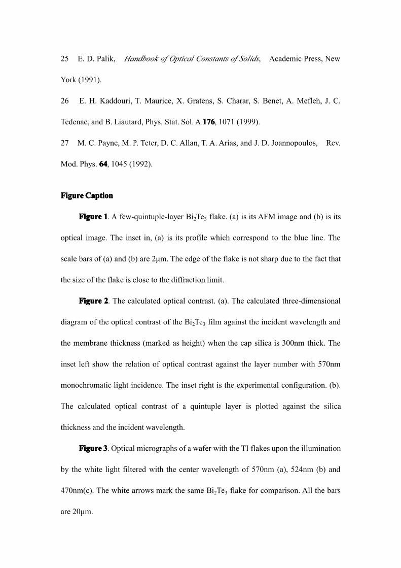
It is quite prominent that the contrast turns reversed after the critical thickness
of 20nm as seen in Fig 2a. In the thinner region of more interests in the layer-
dependent TI behaviors, a saturated reversed contrast is predicted at 13nm (i.e. 13
quintuple layers). The value could be a bit inaccurate because the dielectric response
changes abruptly for the flake with a few quintuple layers5. The normal contrast
increases with increasing the flake thickness in the thicker region as observed in Fig. 3.
It is totally saturated at the thickness of larger than 80nm. Such contrast reversion can
experimentally be observed as shown in FigureFigureFigureFigure 4a4a4a4a, where a sample is illuminated by a
laser at 473nm. The image is obtained by the scanning confocal mode. The few-layer
TI sheets contribute much smaller contrast than the thick flakes, which is predicted to
be around a fifth (Fig 2a). Therefore, more intense source is required to feed the CCD
detector with a better signal/noise ratio than that with the filtered illuminations. AFM
measures the thickness of less than 30nm for the flakes as marked by the white arrows
in Fig 4a. The top one is 20nm thick and the below one is about 5 nm.As compared to
the flakes with the thickness of more than 50nm, one may see the contrast has been

reversed. After the contrast reversion, the thickness-contrast relation is no longer
monotonic. Please see Fig. 1 for the images of the 10nm-thick flake, which contrast is
even stronger than that of the 20nm-thick flake in Fig 4a. All the observations on the
thickness-contrast relation, both the monotonic increase of normal contrast and a
maximized reversed contrast, confirm the theory. We note that even the thin flakes
with as few as 3 quintuple layers can be located by this approach although the contrast
is extremely poor as also expected by the calculation shown in Fig. 2a. Therefore, the
present approach forms a reliable technique to distinguish the few-quintuple-layer
Bi2Te3 sheets by simply reading its contrast.
The applicable range and the error with the approach were assessed in order to
determine the thickness by the optical reading independently. Using the 473-nm-
wavlength laser, we measured dozens of samples for their optical contrast. The
thickness of the flakes were determined by AFM. The experiment data were plotted in
FigureFigureFigureFigure 4b4b4b4b, where we also show the simulated contrast curve using the first-principles
calculated refractive index nth=1.2-2.47i (the red-dot line). The black curve in Fig. 4b
was simulated using the experimentally-determined refractive index nexp=0.84-2.6i.
We can see the consistent trends of all the experimental and theoretical curves. All the
curves present a minimum contrast (nearly zero) in the range of 15-20 QLs. The
systematic deviation between the two calculated curves may be ascribed to the
different refractive index of the subwavelength-thick flakes from that of the bulk5. The
same source applies to the higher experimental contrasts for the few-layer flakes. An
applicable range of the approach is estabilished to be 5-50 QLs, above which no

resolvable difference can be measured. The flakes are no longer TIs below 5 layers14.
In the selected range, the contrast presents a monotone decrease with the increasing
QLs. The errors of such determinations are around 40 percent. The coarse approach
provides a critical and effective locating step in the study of TI Bi2Te3 flakes.
In summary, we have studied visualizing the sub-wavelength-thick Bi2Te3 flakes
by optical imaging the flakes on a capped Si wafer. The added optical length
contributes obvious contrast even for the flake with as few as 3 quintuple layers. We
obtain the layer number-wave length-contrast diagram and the wave length-cap
thickness -contrast diagrams of the thin Bi2Te3 flakes supported by a silica-capped Si
wafer by a calculation based on the Fresnel law. Both the optimized wavelength giving
a commonly maximized contrast and the thickness-dependent contrast reversion have
been demonstrated by our experiments. The present work distinguishes the few-
quintuple-layer Bi2Te3 sheets by simply reading its contrast during the 570nm
illumination and thus provides a critical locating step in the study of TI Bi2Te3 flakes.
We thank the National Natural Science Foundation of China (Grant numbers:
90606002, 11075076, and 10775070) and the National Key Projects for Basic
Research of China (Grant numbers: 2009CB930501, 2010CB923401) for supporting
this project. The Program for New Century Excellent Talents in University of China
Grant No. NCET-07-0422 is also acknowledged.

References&NotesReferences&NotesReferences&NotesReferences&Notes
1 H. J. Goldsmid, J.Appl. Phys. 32323232, 2198 (1961).
2 H. J. GoldSmid, Proc. Phys. Soc. 72727272, 17 (1958).
3 D. Teweldebrhan, V. Goyal, and A.A. Balandin, Nano Lett 10101010, 1209 (2010).
4 V. Goyal, D. Teweldebrhan and A. A. Balandin, Appl. Phys. Lett. 97979797, 133117
(2010).
5 J. Dheepa, R. Sathyamoorthy, and A. Subbarayan, J. Crys. Growth 274274274274, 100
(2005).
6 Y. L. Chen, J. G. Analytis, J. H. Chu, Z. K. Liu, S. K. Mo, X. L. Qi, H. J. Zhang, D.
H. Lu, X. Dai, Z. Fang, S. C. Zhang, I. R. Fisher, Z. Hussain, and Z. X. Shen, Science
325325325325, 178 (2009).
7 D. X. Qu, Y. S. Hor, J. Xiong, R. J. Cava, N. P. Ong, Science 329329329329, 821 (2010).
8 H. J. Zhang, C. X. Liu, X. L. Qi, X. Dai, Z. Fang, and S. C. Zhang, Nat. Phys. 5555,
439 (2009).
9 M. Z. Hasan, C. L. Kane, Rev. Mod. Phys. 82828282, 3045 (2010).
10 X. L. Qi, S. C. Zhang, Physics Today p33, Jan. 2010.
11 J. Moore, Nature 464464464464, 194 (2010).
12 D. Hsieh, Y. Xia, D. Qian, L. Wray, J. H. Dil, F. Meier, J. Osterwalder, L. Patthey,
J. G. Checkelsky, N. P. Ong, A. V. Fedorov, H. Lin, A. Bansil, D. Grauer, Y. S. Hor, R. J.
Cava, and M. Z. Hasan, Nature 444460606060, 1101 (2009).
13 Y. Xia, D. Qian, D. Hsieh, L. Wray, A. Pal, H. Lin, A. Bansil, D. Grauer, Y. S. Hor,
R. J. Cava, and M. Z. Hasan, Nat Phys 5555, 398 (2009).

14 Y. Y. Li, G. Wang, X. G. Zhu, M. H. Liu, C. Ye, X. Chen, Y. Y. Wang, K. He, L. L.
Wang, X. C. Ma, H. J. Zhang, X. Dai, Z. Fang, X. C. Xie, Y. Liu, X. L. Qi, J. F. Jia, S. C.
Zhang, Q. K. Xue, Adv. Mater. 22222222, 4002 (2010).
15 D. Teweldebrhan, V. Goyal, M. Rahman, and A. A. Balandina, Appl. Phys.
Lett. 96969696, 053107 (2010).
16 A. K. Geim and K. S. Novoselov, Nat. Mater. 6666, 183 (2007).
17 R. K. Nkum, A. A. Adimado, and H. Totoe, Mater. Sci. Eng.B 55555555, 102
(1998).
18 Y. B. Xu, Z. M. Ren, W. L. Ren, G. H. Cao, K. Deng, and Y. B. Zhong, Mater
Lett 62626262, 4273 (2008).
19 F. Q. Song, Powles. R., X. F. Wang, N. A. Marks, L. B. He, S. F. Zhao, J. F. Zhou,
Wan. J. G., S. P. Ringer, M. Han, and Wang. G. H., Appl. Phys. Lett. 96969696, 033103 (2010).
20 E. Stolyarova, K. T. Rim, S. M. Ryu, J. Maultzsch, P. Kim, L. E. Brus, T. F. Heinz,
M. S. Hybertsen, and G. W. Flynn, PNAS 104104104104, 9209 (2007).
21 P. Blake, E. W. Hill,A. H. C. Neto, K. S. Novoselov, D. Jiang, R. Yang, T. J. Booth,
and A. K. Geim, Appl. Phys. Lett. 91919191, 063124 (2007).
22 Z. H. Ni, H. M. Wang, J. Kasim, H. M. Fan, T. Yu, Y. H. Wu, Y. P. Feng, and Z. X.
Shen, Nano Letters 7777, 2758 (2007).
23 K. M. F. Shahil, M. Z. Hossain, D. Teweldebrhan, A. A. Balandin, Appl. Phys.
Lett. 96969696, 153103 (2010).
24 D. S. L. Abergel, A. Russell, and V. I. Fal'ko, Appl. Phys. Lett. 91919191, 063125
(2007).
25 E. D. Palik, Handbook of Optical Constants of Solids, Academic Press, New
York (1991).
26 E. H. Kaddouri, T. Maurice, X. Gratens, S. Charar, S. Benet, A. Mefleh, J. C.
Tedenac, and B. Liautard, Phys. Stat. Sol. A 176176176176, 1071 (1999).
27 M. C. Payne, M. P. Teter, D. C. Allan, T. A. Arias, and J. D. Joannopoulos, Rev.
Mod. Phys. 64646464, 1045 (1992).
FigureFigureFigureFigureCaptionCaptionCaptionCaption
FigureFigureFigureFigure 1111. A few-quintuple-layer Bi2Te3 flake. (a) is its AFM image and (b) is its
optical image. The inset in, (a) is its profile which correspond to the blue line. The
scale bars of (a) and (b) are 2μm. The edge of the flake is not sharp due to the fact that
the size of the flake is close to the diffraction limit.
FigureFigureFigureFigure 2222. The calculated optical contrast. (a). The calculated three-dimensional
diagram of the optical contrast of the Bi2Te3 film against the incident wavelength and
the membrane thickness (marked as height) when the cap silica is 300nm thick. The
inset left show the relation of optical contrast against the layer number with 570nm
monochromatic light incidence. The inset right is the experimental configuration. (b).
The calculated optical contrast of a quintuple layer is plotted against the silica
thickness and the incident wavelength.
FigureFigureFigureFigure 3333. Optical micrographs of a wafer with the TI flakes upon the illumination
by the white light filtered with the center wavelength of 570nm (a), 524nm (b) and
470nm(c). The white arrows mark the same Bi2Te3 flake for comparison. All the bars
are 20μm.

FigureFigureFigureFigure 4444. The contrast reversed with the thickness increase. (a). Optical micrograph of
a wafer with many Bi2Te3 flakes illuminated by a low-power blue laser. One can see
the reverse contrasts of some flakes marked by the arrows. The top one measures
20nm thick and the bottom one measures 5nm thick. The width of the micrograph is
around 70μm. (b). The experiment contrast against the quintuple layers (marked as
thickness) with a λ=473nm laser incident. The blue blocks , red-dot line and black line
correspond to the experiment data, first-principle calculation and semi-empirical
calculation, respectively.

LiLiLiLi etetetet alalalal FigFigFigFig 1111

LiLiLiLi etetetet alalalal ,,,, FigFigFigFig 2222

LiLiLiLi etetetet alalalal FigFigFigFig 3333
LiLiLiLi etetetet alalalal ,,,, FigFigFigFig 4444


![β-Cyclodextrin and calix[4]arene-25,26,27,28-tetrol capped carbon dots for selective and sensitive detection of fluoride](https://static.fdokumen.com/doc/165x107/63409d1803ce312bde090e8f/v-cyclodextrin-and-calix4arene-25262728-tetrol-capped-carbon-dots-for-selective.jpg)


