EXPERIMENTAL STUDY OF SUPERCONDUCTING WIRE MOTION ON THE BASE INSULATING MATERIAL IN MAGNETIC FIELD

Charge-carrier transport and recombination in heteroepitaxial CdTeDarius Kuciauskas, Stuart Farrell, Pat Dippo, John Moseley, Helio Moutinho, Jian V. Li, A. M. Allende Motz, AnaKanevce, Katherine Zaunbrecher, Timothy A. Gessert, Dean H. Levi, Wyatt K. Metzger, Eric Colegrove, and S.Sivananthan Citation: Journal of Applied Physics 116, 123108 (2014); doi: 10.1063/1.4896673 View online: http://dx.doi.org/10.1063/1.4896673 View Table of Contents: http://scitation.aip.org/content/aip/journal/jap/116/12?ver=pdfcov Published by the AIP Publishing Articles you may be interested in Effects of hydrogen on majority carrier transport and minority carrier lifetimes in long wavelength infraredHgCdTe on Si Appl. Phys. Lett. 88, 062106 (2006); 10.1063/1.2172295 Above-band gap two-photon absorption and its influence on ultrafast carrier dynamics in ZnTe and CdTe Appl. Phys. Lett. 80, 4771 (2002); 10.1063/1.1489480 Diffusion length in CdTe by measurement of photovoltage spectra in CdS/CdTe solar cells J. Appl. Phys. 89, 460 (2001); 10.1063/1.1332418 Unusually low surface recombination and long bulk lifetime in n-CdTe single crystals Appl. Phys. Lett. 73, 1400 (1998); 10.1063/1.122169 Novel method for growing CdS on CdTe surfaces for passivation of surface states and heterojunction formation J. Vac. Sci. Technol. A 15, 1119 (1997); 10.1116/1.580440
[This article is copyrighted as indicated in the article. Reuse of AIP content is subject to the terms at: http://scitation.aip.org/termsconditions. Downloaded to ] IP:
192.174.37.50 On: Mon, 13 Oct 2014 19:38:58
Charge-carrier transport and recombination in heteroepitaxial CdTe
Darius Kuciauskas,1,a) Stuart Farrell,1 Pat Dippo,1 John Moseley,1 Helio Moutinho,1
Jian V. Li,1 A. M. Allende Motz,1 Ana Kanevce,1 Katherine Zaunbrecher,1
Timothy A. Gessert,1 Dean H. Levi,1 Wyatt K. Metzger,1 Eric Colegrove,2
and S. Sivananthan2
1National Renewable Energy Laboratory, 15013 Denver West Parkway, Golden, Colorado 80401-3305, USA2Microphysics Laboratory, Physics Department, University of Illinois at Chicago, Chicago, Illinois 60612, USA
(Received 6 June 2014; accepted 5 September 2014; published online 26 September 2014)
We analyze charge-carrier dynamics using time-resolved spectroscopy and varying epitaxial
CdTe thickness in undoped heteroepitaxial CdTe/ZnTe/Si. By employing one-photon and nonlin-
ear two-photon excitation, we assess surface, interface, and bulk recombination. Two-photon ex-
citation with a focused laser beam enables characterization of recombination velocity at the
buried epilayer/substrate interface, 17.5 lm from the sample surface. Measurements with a
focused two-photon excitation beam also indicate a fast diffusion component, from which we
estimate an electron mobility of 650 cm2 (Vs)�1 and diffusion coefficient D of 17 cm2 s�1. We
find limiting recombination at the epitaxial film surface (surface recombination velocity
Ssurface¼ (2.8 6 0.3)� 105 cm s�1) and at the heteroepitaxial interface (interface recombination
velocity Sinterface¼ (4.8 6 0.5)� 105 cm s�1). The results demonstrate that reducing surface and
interface recombination velocity is critical for photovoltaic solar cells and electronic devices that
employ epitaxial CdTe. VC 2014 AIP Publishing LLC. [http://dx.doi.org/10.1063/1.4896673]
I. INTRODUCTION
Efficiency of polycrystalline CdTe photovoltaic (PV) so-
lar cells is increasing (current small-area cell record is 21%
by First Solar),1 but it is still much lower than the Shockley-
Queisser limit. Efficiency losses are usually attributed to
charge-carrier recombination, but the nature and location
(bulk, grain boundary, surface/interface) of recombination
centers are not clear.2 Epitaxial materials provide a model
system for the analysis of charge-carrier transport and
recombination. Epilayers have also been used to produce PV
devices. For example, relatively large open-circuit voltage
was achieved with epitaxial Cd1-xZnxTe.3
Heteroepitaxial CdTe/ZnTe/Si has been used for a long
time as substrates for infrared (IR) detectors, but electronic
and recombination properties of this system have not been
studied in detail. Several groups have analyzed defect prop-
erties in heteroepitaxial CdTe using photoluminescence (PL)
spectroscopy.4–6 A key material property relevant for PV
and other electronic devices is minority-carrier lifetime;
however, we are aware of only one photoluminescence-
based measurement of minority-carrier lifetime in epitaxial
CdTe.7 Carrier transport and diffusion in heteroepitaxial
CdTe were also investigated by transient laser-induced gra-
ting spectroscopy.8,9
This paper reports detailed time-resolved photolumines-
cence (TRPL) studies in epitaxial CdTe grown on Si(211)
substrates. We use one-photon and nonlinear two-photon exci-
tation (1PE and 2PE, respectively). By using 1PE, we analyze
surface recombination. In 2PE, generation occurs at the focus
of the laser beam, which enables bulk characterization for
samples with large surface recombination velocity. Combined
1PE and 2PE analysis to determine surface and bulk lifetimes
has been applied to GaN,10,11 ZnSe,12 ZnO,13 diamond,14 and
CdTe.15–17 We extend this approach to characterize the buried
epilayer/substrate interface. Characterization of buried interfa-
ces with a focused 2PE laser beam does not require special
sample preparation, and it avoids contamination or otherwise
changing interface properties.
II. EXPERIMENTAL
A. Sample growth and characterization
To compare and contrast materials grown at different
locations, heteroepitaxial CdTe was grown at the University
of Illinois at Chicago (UIC) and at the National Renewable
Energy Laboratory (NREL).6,18 The substrate for molecular
beam epitaxy (MBE) growth was undoped Si(211), and a
thin (<50 nm) layer of ZnTe was employed to reduce lattice
mismatch between CdTe and the Si substrate while also
maintaining the (211) orientation.6,18 Epilayer thicknesses
were varied from 1.2 to 17.5 lm by altering deposition times
and rates. Final thicknesses were determined by Fourier
transform infrared spectroscopy (FTIR) thin-film interfer-
ence fringes. The full width at half maximum (FWHM) of
double-crystal rocking curve (DCRC) X-ray scans were used
to evaluate the structural quality of all epilayers. For films
thicker than 2 lm, in situ anneal cycles were performed to
improve CdTe structural quality. Cathodoluminescence (CL)
imaging was used to estimate dislocation density.
Panchromatic CL was detected with a Ge photodiode. The
contrast between the dark features and the bright areas was
adjusted visually during the measurement with the contrast
setting on the amplifier for the signal from the Ge diode. In
this way, the brightest and darkest regions approximatelya)[email protected]
0021-8979/2014/116(12)/123108/8/$30.00 VC 2014 AIP Publishing LLC116, 123108-1
JOURNAL OF APPLIED PHYSICS 116, 123108 (2014)
[This article is copyrighted as indicated in the article. Reuse of AIP content is subject to the terms at: http://scitation.aip.org/termsconditions. Downloaded to ] IP:
192.174.37.50 On: Mon, 13 Oct 2014 19:38:58
correspond to the regions of highest and lowest CL intensity.
Some samples were also characterized by electron backscat-
tering diffraction (EBSD). Background doping of
(0.1–1)� 1015 cm�3 was estimated from capacitance-voltage
measurements. Theoretical arguments suggest p-type back-
ground doping because the dominant defect is VCd.2,15 Near-
bandgap PL emission spectra were measured with excitation
at 632.8 nm. A closed-loop liquid helium cryostat was used
for low-temperature PL measurements.
B. Time-resolved photoluminescence measurements
A regeneratively amplified Yb:KGW laser and optical
parametric amplifier (Pharos/Orpheus, Light Conversion)
were used for 1PE and 2PE TRPL measurements. Laser
pulses with 300-fs width were fired at a rate of 1.1 MHz. A
silicon avalanche photodiode (PDM, Micro Photon Devices)
was used for time-correlated single-photon counting (with
Picoharp 300E, PicoQuant). Interference filters (10-nm band-
width, Thorlabs) were used in TRPL signal collection with
820-nm and 840-nm center wavelengths for 820 nm for 1PE
and 2PE measurements, respectively. (The shift in the PL
emission maximum with 2PE is attributed to reabsorption of
the high-energy edge of the CdTe emission spectrum.17) A
dichroic beamsplitter separated collinear excitation and PL
signals. After deconvolution of the instrumental response
function with Fluofit Pro 4.55 software (PicoQuant), we can
resolve lifetimes down to 0.02 ns, which was sufficient for
all samples in this study.
630-nm and 780-nm excitation was used in 1PE meas-
urements. Based on CdTe absorption coefficients19 at these
wavelengths, the generation depth (2.3/a) was 0.5 lm at
630 nm and 1.0 lm at 780 nm.
1120-nm excitation was used in the 2PE measurements.
The two-photon absorption coefficient b is much lower than
the one-photon absorption coefficient a; therefore, carriers
are generated nearly uniformly in the volume defined by the
excitation beam size. Two different 2PE TRPL setups
allowed measurements with relatively large and relatively
small excitation volumes. The optical-fiber-based TRPL
spectrometer employs a 1-m patch of multimode optical fiber
QMMJ-IRVIS-100/140 (OZ Optics) and aspheric lens (New
Focus 5721, NA 0.65), and it has an axial excitation spot di-
ameter of �30 lm.17 Characterization of the ultrafast pulse
delivery for two-photon microscopy with similar QMMJ-
IRVIS-50/125 optical fibers has been reported.20 The 2PE
TRPL measurement with the optical-fiber-based setup pro-
vides approximately uniform volume excitation throughout
the depth of the epitaxial films with a thickness from 1.2 to
17.5 lm.
For high-spatial-resolution 2PE TRPL measurements, an
A-Plan 40� NA0.65 microscope objective (Zeiss) with good
near-IR transmittance was used. The laser beam was
expanded using a telescope to slightly overfill the micro-
scope aperture. The telescope magnification ratio was
adjusted to obtain the best spatial resolution, and the sample
was axially translated with a computer-controlled linear
translation stage employing a motorized actuator Z812B
(Thorlabs, minimal incremental movement of 0.05 lm,
bidirectional repeatability <1.5 lm). An axial resolution of
5.5 6 0.9 lm (1/e2 width) for this setup was estimated from
axial scans through the surface of the epitaxial CdTe sample.
This axial resolution corresponds to 2.0 6 0.3 lm lateral re-
solution, and this number was used in the data analysis.
For TRPL data analysis, the optical resolution needs to
be compared with the diffusion length, L, for photogenerated
carriers. For samples studied here, L is larger than 2 lm but
less than 30 lm (see Sec. III D); therefore, we are able to
investigate carrier transport from high-spatial-resolution
TRPL measurements and recombination from low-spatial-re-
solution measurements.
III. RESULTS AND DISCUSSION
A. Low-temperature PL emission spectra
EBSD showed that CdTe epilayers have (211) orienta-
tion. The misalignment between the [211] direction and the
surface normal was �5�. Samples had good crystallinity
indicated by high-quality Kikuchi patterns and by pole fig-
ures with minimum orientation spread. Grains or domains of
different orientation were not observed.
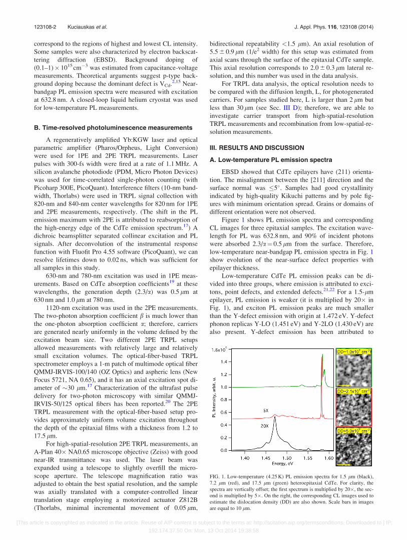
Figure 1 shows PL emission spectra and corresponding
CL images for three epitaxial samples. The excitation wave-
length for PL was 632.8 nm, and 90% of incident photons
were absorbed 2.3/a¼ 0.5 lm from the surface. Therefore,
low-temperature near-bandgap PL emission spectra in Fig. 1
show evolution of the near-surface defect properties with
epilayer thickness.
Low-temperature CdTe PL emission peaks can be di-
vided into three groups, where emission is attributed to exci-
tons, point defects, and extended defects.21,22 For a 1.5-lm
epilayer, PL emission is weaker (it is multiplied by 20� in
Fig. 1), and exciton PL emission peaks are much smaller
than the Y-defect emission with origin at 1.472 eV. Y-defect
phonon replicas Y-LO (1.451 eV) and Y-2LO (1.430 eV) are
also present. Y-defect emission has been attributed to
FIG. 1. Low-temperature (4.25 K) PL emission spectra for 1.5 lm (black),
7.2 lm (red), and 17.5 lm (green) heteroepitaxial CdTe. For clarity, the
spectra are vertically offset; the first spectrum is multiplied by 20�, the sec-
ond is multiplied by 5�. On the right, the corresponding CL images used to
estimate the dislocation density (DD) are also shown. Scale bars in images
are equal to 10 lm.
123108-2 Kuciauskas et al. J. Appl. Phys. 116, 123108 (2014)
[This article is copyrighted as indicated in the article. Reuse of AIP content is subject to the terms at: http://scitation.aip.org/termsconditions. Downloaded to ] IP:
192.174.37.50 On: Mon, 13 Oct 2014 19:38:58

dislocations in epitaxial4,5 and single-crystal CdTe.23,24
Therefore, the PL emission spectrum for the 1.5-lm epilayer
is dominated by dislocations. CL analysis shows that the sur-
face dislocation density for this sample was >5� 107 cm�2.
For the epilayer with 7.2-lm thickness, both the Y-
defect and exciton emission peaks are present. The PL emis-
sion is stronger than the 1.2-lm epilayer, but weaker than
the 17.5-lm epilayer. The dislocation density from the CL
analysis was 2.1� 107 cm�2.
For the 17.5-lm epilayer, the dislocation density is fur-
ther reduced to 1� 107 cm�2. Here, exciton PL emission is
dominant. Peaks at 1.594 (FX), 1.589 eV (DX), 1.587 eV
(A1X), and 1.585 eV (A2X) are attributed to free excitons,
donor-bound excitons, and acceptor-bound excitons, respec-
tively.21,22 Smaller-amplitude PL emission peaks are attrib-
uted to phonon replicas at 1.574 eV (FX-LO), 1.571 eV
(A1X-LO), and 1.564 eV (A2X-LO).
Rujirawat et al. and Chen et al. have presented detailed
structural analysis for heteroepitaxial CdTe/ZnTe/Si.6,18
They found that large lattice mismatch introduces up to
1013 cm�2 misfit dislocations at the CdTe/ZnTe/Si heteroepi-
taxial interface region. Many of these dislocations are tan-
gled and annihilate near the interface. Thereafter, threading
dislocations propagate in the epitaxial layer and dislocation
density decreases inversely with layer thickness. In their
samples, dislocation density decreased to �3� 107 cm�2
about 3 lm from the CdTe/ZnTe/Si interface region.6,16
Similar to the study by Chen et al.,6 we observe evolution of
low-temperature PL emission spectra from Y-defect emis-
sion to exciton-dominated emission. Based on these data, it
is clear that dislocations dominate PL emission for 1–2-lm-
thick epilayers and are present to a lesser degree in thicker
epilayers. In Sec. III D, we investigate their effect on charge-
carrier dynamics.
At room temperature, PL emission (with maximum at
1.50 eV) is attributed to band-to-band recombination.
Radiative efficiency is low, and nonradiative recombination
largely determines overall recombination rate.
B. Recombination near the surface
TRPL decays for the 7.2-lm epilayer sample are shown
in Fig. 2. 1PE decays can be described as two-exponential.
Lifetimes measured with 630-nm excitation are s1¼ 0.08 ns
(A1¼ 0.87 of total amplitude) and s2¼ 0.44 ns (A2¼ 0.13).
The corresponding lifetimes for 780-nm excitation are
s1¼ 0.14 ns (A1¼ 0.80) and s2¼ 0.57 ns (A2¼ 0.20).
Average lifetimes calculated from the formula
sav¼A1s1þA2s2 are 0.13 and 0.23 ns for 630-nm and 780-
nm excitation, respectively. 1PE TRPL decays were essen-
tially the same when the excitation intensity was varied from
(0.5–2.0)� 1013 photons cm�2 pulse�1. In the case of sur-
face recombination (see below), the excitation-intensity-
independent lifetimes do not indicate trap saturation.
Biexponential 1PE TRPL decay shape is indicative of
high surface recombination velocity.11,17 After the laser
pulse generates carriers in the sample, the time evolution of
carrier concentration is governed by drift, diffusion, and
recombination, and solutions to a diffusion equation for
photogenerated carriers need to be considered in TRPL data
analysis.12,25,27–29 From solutions in the one-dimensional
case, Ahrenkiel and Dashdorj have determined that the
initial decay rate can be described as25
1
s1
¼ 1
sBþ aS; (1)
where sB is bulk lifetime and S is surface recombination ve-
locity. The first and second terms describe bulk and surface
recombination rates, respectively. For high-quality single-
crystal CdTe, aS � sB�1 and S can be estimated from the
experimental s1 value.17 The diffusion lengths, L, corre-
sponding to lifetimes s1 are very short: L¼ 0.36 lm (630-nm
excitation) and L¼ 0.49 lm (780-nm excitation; diffusion
coefficient D¼ 17 cm2/s is estimated in Sec. III D). Both val-
ues are similar to absorption depths (2.3/a630nm and 2.3/
a780nm); therefore, data suggest that the majority of the pho-
togenerated carriers recombine close to the sample surface.
Wang et al. solved the diffusion equation for photogen-
erated carriers using a Fourier transform method and eval-
uated different non-exponential decay terms.12 They found
that the dominant lifetime can be described by the equation12
1
sav¼ 1
sBþ 2a2D
1þffiffiffiffiffiffiffiffiffiffiffiffiffiffiffiffiffiffiffiffiffiffiffiffiffiffi1þ 8a2D=S2
p � 1
sBþ affiffiffi
2p S: (2)
The simplified form can be used when 8a2D2/S2� 1. Based
on the value for D estimated in Sec. III D and the value for S
estimated in the paragraph below, 8a2D2/S2� 60 for 630-nm
excitation and �30 for 780-nm excitation.
Surface recombination terms in Eqs. (1) and (2) differ
by a factor of �2, which could be attributed to different
approaches used in deriving the equations. Ahrenkiel and
Dashdorj have estimated the initial decay rate, whereas
Wang et al. have considered the dominant decay rate.
Therefore, to estimate S, we use s1 in Eq. (1) and sav in Eq.
(2). This yields S¼ 2.8� 105 cm s�1 (s1, 630 nm),
FIG. 2. 1PE and 2PE TRPL decays for 7.2 lm epilayer. 1PE excitation in-
tensity was 1.0� 1013 photons cm�2 pulse�1; 2PE excitation intensity was
1.5 � 1016 photons cm�2 pulse�1.
123108-3 Kuciauskas et al. J. Appl. Phys. 116, 123108 (2014)
[This article is copyrighted as indicated in the article. Reuse of AIP content is subject to the terms at: http://scitation.aip.org/termsconditions. Downloaded to ] IP:
192.174.37.50 On: Mon, 13 Oct 2014 19:38:58
S¼ 3.1� 105 cm s�1 (s1, 780 nm), S¼ 2.5� 105 cm s�1 (sav,
630 nm), and S¼ 2.7� 105 cm s�1 (sav, 780 nm). The aver-
age value is S¼ (2.8 6 0.3)� 105 cm s�1.
Very similar 1PE TRPL data were obtained for the other
epitaxial samples. Within the error of measurement, 1PE TRPL
decays were independent of the epilayer thickness. This sug-
gests that S was similar for all samples in this series. However,
the dislocation density strongly depends on epilayer thickness
(Fig. 1). Hence, these data suggest that recombination occurs at
other surface defects and not only at dislocations.
The surface recombination velocity for epitaxial CdTe
is similar to that for other single-crystal or epitaxial semicon-
ductors. For example, from PL-based analyses,
S¼ (1–3)� 104 cm s�1 for GaN,11 S¼ 5.8� 105 cm s�1 for
ZnSe,12 S¼ 1.0� 106 cm s�1 for diamond,14 and
S¼ 3� 106 cm s�1 for GaAs.26 Using nonlinear four-wave
mixing measurements, it was determined that
S¼ 3� 106 cm s�1 for CdTe,9 S¼ (0.2–5)� 105 cm s�1 for
InP,30 and S¼ (0.3�3)� 106 cm s�1 for GaAs.30
C. Recombination for uniform generation with 2PE
The 1PE TRPL data described above provide estimates
for S at the surface of the epitaxial sample, but the data are
independent of the epitaxial layer thickness. To study bulk
properties, we employ 2PE, where generation happens at the
laser-beam focus. This section describes measurements
where the generation volume axially spans the entire epitax-
ial layer. In Sec. III D, we describe measurements with 5.5-
lm axial and 2.0-lm lateral spatial resolution, where genera-
tion volume can be selectively placed in the bulk.
The 2PE TRPL decay for the 7.5-lm sample (see Fig. 2)
can be described as single-exponential with s2PE¼ 0.83 ns,
but these data alone do not establish if recombination has
occurred in the absorber bulk or at interfaces. To learn about
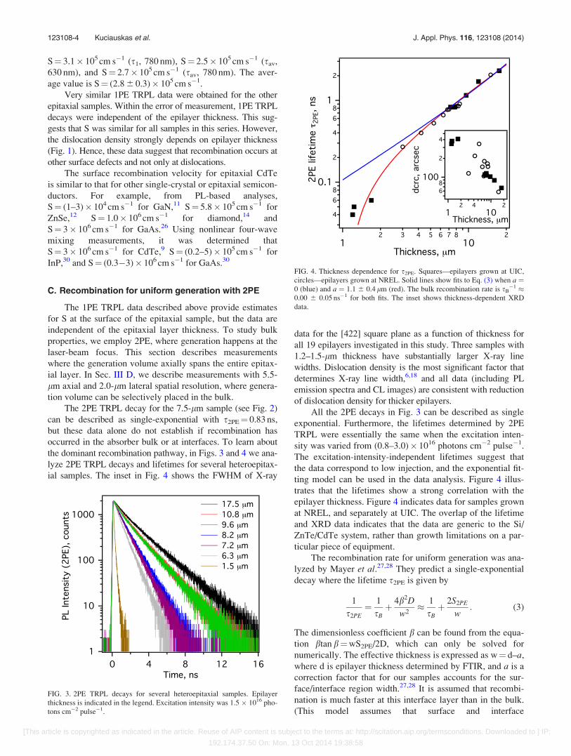
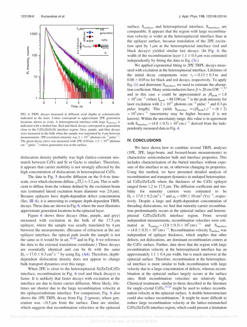
the dominant recombination pathway, in Figs. 3 and 4 we ana-
lyze 2PE TRPL decays and lifetimes for several heteroepitax-
ial samples. The inset in Fig. 4 shows the FWHM of X-ray
data for the [422] square plane as a function of thickness for
all 19 epilayers investigated in this study. Three samples with
1.2–1.5-lm thickness have substantially larger X-ray line
widths. Dislocation density is the most significant factor that
determines X-ray line width,6,18 and all data (including PL
emission spectra and CL images) are consistent with reduction
of dislocation density for thicker epilayers.
All the 2PE decays in Fig. 3 can be described as single
exponential. Furthermore, the lifetimes determined by 2PE
TRPL were essentially the same when the excitation inten-
sity was varied from (0.8–3.0)� 1016 photons cm�2 pulse�1.
The excitation-intensity-independent lifetimes suggest that
the data correspond to low injection, and the exponential fit-
ting model can be used in the data analysis. Figure 4 illus-
trates that the lifetimes show a strong correlation with the
epilayer thickness. Figure 4 indicates data for samples grown
at NREL, and separately at UIC. The overlap of the lifetime
and XRD data indicates that the data are generic to the Si/
ZnTe/CdTe system, rather than growth limitations on a par-
ticular piece of equipment.
The recombination rate for uniform generation was ana-
lyzed by Mayer et al.27,28 They predict a single-exponential
decay where the lifetime s2PE is given by
1
s2PE¼ 1
sBþ 4b2D
w2� 1
sBþ 2S2PE
w: (3)
The dimensionless coefficient b can be found from the equa-
tion btan b¼wS2PE/2D, which can only be solved for
numerically. The effective thickness is expressed as w¼ d–a,
where d is epilayer thickness determined by FTIR, and a is a
correction factor that for our samples accounts for the sur-
face/interface region width.27,28 It is assumed that recombi-
nation is much faster at this interface layer than in the bulk.
(This model assumes that surface and interface
FIG. 3. 2PE TRPL decays for several heteroepitaxial samples. Epilayer
thickness is indicated in the legend. Excitation intensity was 1.5 � 1016 pho-
tons cm�2 pulse�1.
FIG. 4. Thickness dependence for s2PE. Squares—epilayers grown at UIC,
circles—epilayers grown at NREL. Solid lines show fits to Eq. (3) when a ¼0 (blue) and a ¼ 1.1 6 0.4 lm (red). The bulk recombination rate is sB
�1 �0.00 6 0.05 ns�1 for both fits. The inset shows thickness-dependent XRD
data.
123108-4 Kuciauskas et al. J. Appl. Phys. 116, 123108 (2014)
[This article is copyrighted as indicated in the article. Reuse of AIP content is subject to the terms at: http://scitation.aip.org/termsconditions. Downloaded to ] IP:
192.174.37.50 On: Mon, 13 Oct 2014 19:38:58
recombination velocities are the same. Independent estimate
of recombination velocity at the buried CdTe/ZnTe/Si inter-
face region is given in Sec. III D, Fig. 6.) The simplified
form of Eq. (3) is also widely used in the TRPL data analysis
for double heterostructures.29 The difference is that for dou-
ble heterostructures, a� 0 and w¼ d.
This formula provides three plausible explanations for
the 2PE lifetime data in Fig. 4. The first explanation is that
interface recombination is dominant. The second explanation
is that the defect density is inversely proportional to the
thickness and drives bulk lifetime. The XRD FWHM is pro-
portional to the defect density, and the XRD data in Fig. 4
are clearly inversely proportional to the epilayer thickness.
This makes sense because as thickness increases, threading
dislocations annihilate. The third possibility is that both
mechanisms contribute.
We will assume at first that interface recombination is
dominant. Figure 4 shows fits according to the simplified
form of Eq. (3). The blue solid line corresponds to w¼ d
and does not fit well for samples with thickness in the
1.2–1.5-lm range. The red solid line corresponds to
a¼ 1.1 6 0.4 lm and gives a better fit. For samples with
large lattice constant mismatch, such as CdTe/ZnTe/Si, the
highly defective surface/interface region can extend deeply
into the absorber.6,18 This was evident in Fig. 1, where the
1.5-lm epilayer had only weak PL emission dominated by
dislocations. Presumably, these dislocations have propagated
from the CdTe/ZnTe/Si interface region. All 1.2–1.5-lm-
thick samples had this feature, and we can expect that the
value for a will be in this range.
These data also provide estimate for a recombination
velocity near the buried interface. Both fits yield
S2PE¼ (3.8 6 0.4)� 105 cm s�1, which is similar to the esti-
mate from the 1PE TRPL measurement (Fig. 2,
S¼ (2.8 6 0.3)� 105 cm s�1). 2PE data were measured at
lower injection than 1PE data; this might be one of the rea-
sons for some difference in S values. It is also possible that
Sinterface (at the CdTe/ZnTe/Si interface region) is larger than
the Ssurface at CdTe surface. Therefore, we can estimate
Ssurface¼ (2.8 6 0.3)� 105 cm s�1 from 1PE measurements,
and Sinterface¼ 2S2PE – Ssurface¼ (4.8 6 0.5)� 105 cm s�1
from fits to data in Fig. 4.
Next, we consider bulk lifetime sB. If dislocations act as
Shockley-Read-Hall (SRH) recombination centers, as the CL
data indicates, then one expects that sB would be depth-
dependent. Data in Fig. 4 do not allow us to distinguish
unambiguously how bulk lifetime may contribute to the
overall lifetime. However, the 1PE data do allow us to con-
clude that aggregate recombination is significantly limited
by the surface. Interestingly, diffusion for photogenerated
carriers must be sufficiently fast to allow transport to the sur-
face over the distance of 8 lm (for carriers generated at the
midpoint of the 17.5-lm epilayer). To learn more about
transport, we performed initial Sentaurus Device simulations
for TRPL decays.33 Simulations indicate that for electron
mobility of 650 cm2 (Vs)�1 (see Sec. III D below) bulk life-
time of 50 ns is required for carriers to diffuse over the dis-
tance of 8 lm. For shorter lifetimes, fewer carriers will
reach the interface. An analytical model relating depth-
dependent dislocation concentration to SRH lifetime is nec-
essary for a more-detailed computational analysis. This work
will be reported in the future.
To better characterize the heteroepitaxial interface and
carrier transport in the bulk, Sec. III D describes direct mi-
croscopic measurements.
D. Recombination and transport for generation with afocused excitation beam
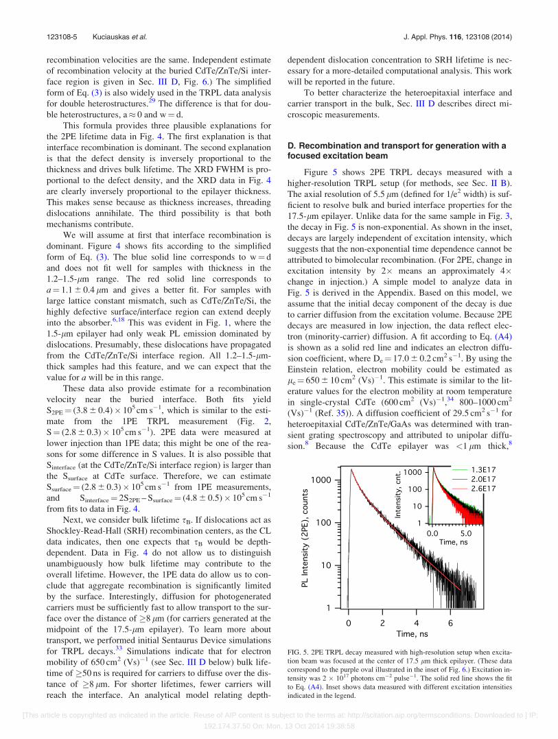
Figure 5 shows 2PE TRPL decays measured with a
higher-resolution TRPL setup (for methods, see Sec. II B).
The axial resolution of 5.5 lm (defined for 1/e2 width) is suf-
ficient to resolve bulk and buried interface properties for the
17.5-lm epilayer. Unlike data for the same sample in Fig. 3,
the decay in Fig. 5 is non-exponential. As shown in the inset,
decays are largely independent of excitation intensity, which
suggests that the non-exponential time dependence cannot be
attributed to bimolecular recombination. (For 2PE, change in
excitation intensity by 2� means an approximately 4�change in injection.) A simple model to analyze data in
Fig. 5 is derived in the Appendix. Based on this model, we
assume that the initial decay component of the decay is due
to carrier diffusion from the excitation volume. Because 2PE
decays are measured in low injection, the data reflect elec-
tron (minority-carrier) diffusion. A fit according to Eq. (A4)
is shown as a solid red line and indicates an electron diffu-
sion coefficient, where De¼ 17.0 6 0.2 cm2 s�1. By using the
Einstein relation, electron mobility could be estimated as
le¼ 650 6 10 cm2 (Vs)�1. This estimate is similar to the lit-
erature values for the electron mobility at room temperature
in single-crystal CdTe (600 cm2 (Vs)�1,34 800–1000 cm2
(Vs)�1 (Ref. 35)). A diffusion coefficient of 29.5 cm2 s�1 for
heteroepitaxial CdTe/ZnTe/GaAs was determined with tran-
sient grating spectroscopy and attributed to unipolar diffu-
sion.8 Because the CdTe epilayer was <1 lm thick,8
FIG. 5. 2PE TRPL decay measured with high-resolution setup when excita-
tion beam was focused at the center of 17.5 lm thick epilayer. (These data
correspond to the purple oval illustrated in the inset of Fig. 6.) Excitation in-
tensity was 2 � 1017 photons cm�2 pulse�1. The solid red line shows the fit
to Eq. (A4). Inset shows data measured with different excitation intensities
indicated in the legend.
123108-5 Kuciauskas et al. J. Appl. Phys. 116, 123108 (2014)
[This article is copyrighted as indicated in the article. Reuse of AIP content is subject to the terms at: http://scitation.aip.org/termsconditions. Downloaded to ] IP:
192.174.37.50 On: Mon, 13 Oct 2014 19:38:58
dislocation density probably was high (lattice-constant mis-
match between CdTe and Si or GaAs is similar). Therefore,
it appears that carrier mobility is not strongly affected by the
high concentration of dislocations in heteroepitaxial CdTe.
The data in Fig. 5 describe diffusion on the 0–6-ns time-
scale, over which electrons diffuseffiffiffiffiffiffiffiDetp
� 3.2 lm. This is suffi-
cient to diffuse from the volume defined by the excitation beam
size (estimated lateral excitation beam diameter was 2.0lm).
Because epilayers have depth-dependent defect concentration
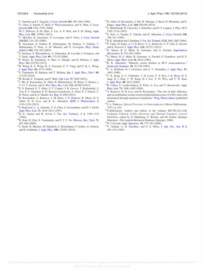
(Sec. III A), it is interesting to compare depth-dependent TRPL
decays. These data are shown in Fig. 6, where the inset illustrates
approximate generation locations in the epitaxial layer.
Figure 6 shows three decays (blue, purple, and grey)
measured with excitation in the bulk of the 17.5-lm
epilayer, where the sample was axially translated by 4 lm
between the measurements. (Because of refraction at the air/
epilayer interface, the optical path inside the sample is not
the same as it would be in air,16,36 and in Fig. 6 we reference
the data to the external translation coordinate.) Three decays
are essentially identical and can be fit with the same
De¼ 17.0 6 0.3 cm2 s�1 by using Eq. (A4). Therefore, depth-
dependent dislocation density does not appear to change
bulk transport dynamics over this range.
When 2PE is close to the heteroepitaxial Si/ZnTe/CdTe
interface, recombination in Fig. 6 (red and black decays) is
faster. It is unlikely that faster decays with excitation at the
interface are due to faster carrier diffusion. More likely, life-
times are shorter due to the large recombination velocity at
the epilayer/substrate interface. For comparison, Fig. 6 also
shows the 1PE TRPL decay from Fig. 2 (green), where gen-
eration was <0.5 lm from the surface. Data are similar,
which suggests that recombination velocities at the epitaxial
surface, Ssurface, and heteroepitaxial interface, Sinterface, are
comparable. It appears that the region with large recombina-
tion velocity is wider at the heteroepitaxial interface than at
the epilayer surface, because translation of the 2PE excita-
tion spot by 1 lm at the heteroepitaxial interface (red and
black decays) yielded similar fast decays. (In Fig. 4, the
width of the recombination layer 1.1 6 0.4 lm was estimated
independently by fitting the data to Eq. (3).)
We applied exponential fitting to 2PE TRPL decays meas-
ured with excitation at the heteroepitaxial interface. Lifetimes of
the initial decay components were s1¼ 0.13 6 0.3 ns and
0.08 6 0.05 ns for black and red decays, respectively. To apply
Eq. (1) and determine Sinterface, we need to estimate the absorp-
tion coefficient. Many semiconductors have b� 20 cm GW�1,37
and in this case a could be approximated as bIpeak¼ 1.8
� 103cm�1 (where Ipeak¼ 88 GWcm�2 is the peak intensity for
laser excitation with 2� 1017 photons cm�2 pulse�1 and 0.3-ps
pulse length). This yields Sinterface � (bIpeaks1)–1¼ (6 6 2)
� 105cm s�1 (uncertainty may be higher because b is not
known). Within the uncertainty range, this value is in agreement
with Sinterface¼ (4.8 6 0.5)� 105cm s�1 derived from the inde-
pendently measured data in Fig. 4.
IV. CONCLUSIONS
We have shown how to combine several TRPL analyses
(1PE, 2PE, large-beam, and focused-beam measurements) to
characterize semiconductor bulk and interface properties. This
includes characterization of the buried interface without expo-
sure of this interface to air, or otherwise changing its properties.
Using this method, we have presented detailed analysis of
recombination and transport dynamics in undoped heteroepitax-
ial CdTe/ZnTe/Si where the thickness of the CdTe epilayer
ranged from 1.2 to 17.5 lm. The diffusion coefficient and mo-
bility for minority carriers were estimated to be
De¼ 17.0 6 0.2 cm2 s�1 and le¼ 650 6 10 cm2 (Vs)�1, respec-
tively. Despite a large and depth-dependent concentration of
threading dislocations, we find that minority-carrier recombina-
tion predominantly occurs at the epitaxial surface and heteroe-
pitaxial CdTe/ZnTe/Si interface region. From several
independent measurements, recombination velocities were esti-
mated as Ssurface¼ (2.8 6 0.3)� 105cm s�1 and Sinterface
¼ (4.8 6 0.5)� 105cm s�1. Recombination velocity Ssurface was
independent of epilayer thickness, which implies that other
defects, not dislocations, are dominant recombination centers at
the CdTe surface. Further, data show that the region with large
recombination velocity at the heteroepitaxial interface has an
approximately 1.1 6 0.4 lm width, but is much narrower at the
epitaxial surface. Therefore, recombination at the heteroepitax-
ial interface is more similar to bulk recombination with large
velocity due to a large concentration of defects, whereas recom-
bination at the epitaxial surface largely occurs at the surface
sites. Both recombination velocities are relatively high.
Chemical treatments, similar to those described in the literature
for single-crystal CdTe,31,32 might be used to reduce recombi-
nation velocity at the epitaxial surface. A double heterostructure
could also reduce recombination.7 It might be more difficult to
reduce large recombination velocity at the lattice-mismatched
CdTe/ZnTe/Si interface region, which could present a limitation
FIG. 6. TRPL decays measured at different axial depths as schematically
indicated in the inset. Colors correspond to approximate 2PE generation
locations shown as ovals. A heteroepitaxial interface with large Sinterface is
indicated with a dashed line. Red and black decays correspond to generation
close to the CdTe/ZnTe/Si interface region. Grey, purple, and blue decays
were measured in the bulk when the sample was translated by 4 lm between
measurements. 2PE excitation intensity was 2 � 1017 photons cm�2 pulse�1.
The green decay curve was measured with 1PE (630 nm, 1.5 � 1016 photons
cm�2 pulse�1) where generation was at the surface.
123108-6 Kuciauskas et al. J. Appl. Phys. 116, 123108 (2014)
[This article is copyrighted as indicated in the article. Reuse of AIP content is subject to the terms at: http://scitation.aip.org/termsconditions. Downloaded to ] IP:
192.174.37.50 On: Mon, 13 Oct 2014 19:38:58

for PV and other electronic devices that employ epitaxial CdTe
grown on Si substrates.
ACKNOWLEDGMENTS
This work was supported by the U.S. Department of
Energy under Contract No. DE-AC36-08-GO28308 with the
National Renewable Energy Laboratory.
APPENDIX: ESTIMATING DIFFUSION COEFFICIENTFROM 2PE TRPL DATA WHEN CARRIER DIFFUSIONLENGTH IS LARGER THAN THE EXCITATION BEAMDIAMETER
We assume an exponential decay for PL signal intensity,
I(t)29
I tð Þ ¼ I0e� t
sB ; (A1)
where I0 is initial PL intensity, t is time, and sB is lifetime.
Data in Fig. 3 are in good agreement with this model.
Agreement is expected because, in this case, carriers are gen-
erated uniformly in a volume that spans the entire sample
thickness, and carrier diffusion length L is smaller than the
excitation beam diameter. Data are more complex when the
measurement is carried out with a focused laser beam of ra-
dius u (Figs. 5 and 6). Here, we derive a simple model to
explain these data by accounting for carrier diffusion.
In the collinear measurement geometry shown in Fig. 7,
excitation (generation) and PL measurement volumes are
assumed to be the same. Photogenerated carriers will diffuse
from the initial excitation volume, which will decrease PL sig-
nal intensity. One-dimensional diffusion can be described by
I x; tð Þ ¼I tð Þ
2ffiffiffiffiffiffiffiffipDtp exp � x2
4Dt
� �; (A2)
where D is diffusion coefficient and x is the coordinate.
(This expression could be generalized for two-dimensional
lateral diffusion by multiplying it by angle 2p. Because am-
plitude I0 is an adjustable parameter in data analysis, the
result would be the same.)
Excitation pulses and Icollected follow the same optical
path (but in opposite directions). Therefore, we assume that
for carriers that diffused laterally from the excitation
volume, photons emitted after radiative recombination will
not be detected in the TRPL measurement. We neglect con-
tributions to Icollected due to PL scattered in the sample. For
high-quality single-crystals, scattering is expected to be
weak. We further simplify the problem by assuming that PL
is only collected from the rectangle indicated by dashed lines
in Fig. 7. Under these assumptions, the experimentally meas-
ured PL signal, Icollected(t), will be
Icollected tð Þ ¼ I0e�t
sB
2ffiffiffiffiffiffiffiffipDtp
ðu
�u
exp � x2
4Dt
� �dx: (A3)
After integration, time-dependent PL intensity is
Icollected tð Þ ¼ I0erfu
2ffiffiffiffiffiDtp
� �e� t
sB : (A4)
Data analysis with Eq. (A4) is shown in Fig. 5. The error
function primarily determines decay shape at early times, and
fitting provides estimates for D. At low injection, the esti-
mated diffusion coefficient is for minority carriers, De. At suf-
ficiently long time delays after excitation, the error-function
argument is small, and Eq. (A4) could be simplified as
Icollected tð Þ � I0u
2ffiffiffiffiffiDtp e
� tsB : (A5)
Therefore, TRPL decays measured with a focused exci-
tation beam (when u�L) will be non-exponential at all time-
scales. Data in Figs. 5 and 6 support this conclusion.
In summary, measurement with a focused laser beam
allows estimating transport parameters (D and l by using the
Einstein relation), but sB is determined more reliably when
the excitation spot diameter is larger than L. Combined 2PE
TRPL measurements with large (Fig. 3) and focused (Figs. 5
and 6) laser beams provide for characterization of both trans-
port (l and D) and lifetime (sB).
This model makes several assumptions and simplifica-
tions. First, we did not consider excitation-beam refraction.36
In principle, refraction effects could be reduced by using an
oil-immersion objective or solid-immersion lens.36 Second,
the model does not account for reabsorption. Reabsorption
will affect axial resolution for the measurement, but will
have a smaller effect on lateral resolution. Third, the model
does not consider diffraction, and Eq. (A4) could only be
used when L is larger than the Abbe diffraction limit. Fourth,
we assumed that a surface-induced electric field is not pres-
ent; therefore, drift was not considered.
1See http://investor.firstsolar.com/releasedetail.cfm?ReleaseID¼864426 for
reported CdTe photovoltaic solar cell efficiency (accessed August 15,
2014).2T. A. Gessert, S.-H. Wei, J. Ma, D. S. Albin, R. G. Dhere, J. N. Duenow,
D. Kuciauskas, A. Kanevce, T. M. Barnes, J. M. Burst, W. L. Rance, M.
O. Reese, and H. R. Moutinho, Sol. Energy Mater. Sol. Cells 119,
149–155 (2013).3M. Carmody, S. Mallick, J. Magetis, R. Kodama, T. Biegala, D. Xu, P.
Bechmann, J. W. Garland, and S. Sivananthan, Appl. Phys. Lett. 96,
153502 (2010).4P. J. Dean, G. M. Williams, and G. Blackmore, J. Phys. D: Appl. Phys. 17,
2291–2300 (1984).
FIG. 7. Illustration of 2PE carrier generation with a focused laser beam (red
oval). Lateral diffusion (coordinate x) from this volume reduces intensity of
photoluminescence Icollected. Dashed lines indicate integration limits used to
estimate Icollected.
123108-7 Kuciauskas et al. J. Appl. Phys. 116, 123108 (2014)
[This article is copyrighted as indicated in the article. Reuse of AIP content is subject to the terms at: http://scitation.aip.org/termsconditions. Downloaded to ] IP:
192.174.37.50 On: Mon, 13 Oct 2014 19:38:58
5C. Onodera and T. Taguchi, J. Cryst. Growth 101, 502–506 (1990).6Y. Chen, S. Farrell, G. Brill, P. Wijewarnasuriya, and N. Dhar, J. Cryst.
Growth 310, 5303–5307 (2008).7M. J. DiNezza, X.-H. Zhao, S. Liu, A. P. Kirk, and Y.-H. Zhang, Appl.
Phys. Lett. 103, 193901 (2013).8V. Mizeikis, K. Jarasiunas, N. Lovergine, and P. Prete, J. Cryst. Growth
214/215, 234–239 (2000).9K. Jarasiunas, E. Gaubas, R. Aleksiejunas, M. Sudzius, V. Gudelis, T.
Malinauskas, P. Prete, A. M. Mansini, and N. Lovergine, Phys. Status
Solidi A 195, 238–242 (2003).10S. Jur�s _enas, S. Miasojedovas, A. �Zukauskas, B. Lucznik, I. Grzegory, and
T. Suski, Appl. Phys. Lett. 89, 172119 (2006).11P. �Scajev, K. Jara�si�unas, S. Okur, U. O€uzg€ur, and H. Morkoc, J. Appl.
Phys. 111, 023702 (2012).12H. Wang, K. S. Wong, B. A. Foreman, Z. Y. Yang, and G. K. L. Wong,
J. Appl. Phys. 83, 4773 (1998).13S. Yamamoto, H. Sakuma, and T. Mishina, Jpn. J. Appl. Phys., Part 1 49,
121102 (2010).14M. Koz�ak, F. Troj�anek, and P. Mal�y, Opt. Lett. 37, 2049 (2012).15J. Ma, D. Kuciauskas, D. Albin, R. Bhattacharya, M. Reese, T. Barnes, J.
V. Li, T. Gessert, and S. Wei, Phys. Rev. Lett. 111, 067402 (2013).16E. S. Barnard, E. T. Hoke, S. T. Connor, J. R. Groves, T. Kuykendall, Z.
Yan, E. C. Samulon, E. D. Bourret-Courchesne, S. Aloni, P. J. Schuck, C.
H. Peters, and B. E. Hardin, Sci. Rep. 3, 2098 (2013).17D. Kuciauskas, A. Kanevce, J. M. Burst, J. N. Duenow, R. Dhere, D. S.
Albin, D. H. Levi, and R. K. Ahrenkiel, IEEE J. Photovoltaics 3,
1319–1324 (2013).18S. Rujirawat, L. A. Almeida, Y. P. Chen, S. Sivananthan, and D. J. Smith,
Appl. Phys. Lett. 71, 1810–1812 (1997).19D. E. Aspnes and H. Arwin, J. Vac. Sci. Technol., A 2, 1309–1315
(1984).20D. Kim, H. Choi, S. Yazdanafar, and P. T. C. So, Microsc. Res. Tech. 71,
887–896 (2008).21C. Kraft, H. Metzner, M. Ha€udrich, U. Reislo€uhner, P. Schley, G. Gobsch,
and R. Goldhahn, J. Appl. Phys. 108, 124503 (2010).
22D. Albin, D. Kuciauskas, J. Ma, W. Metzger, J. Burst, H. Moutinho, and P.
Dippo, Appl. Phys. Lett. 104, 092109 (2014).23S. Hildebrandt, H. Uniewski, J. Schreiber, and H. S. Leipner, J. Phys. III 7,
1505–1514 (1997).24S. Seto, A. Tanaka, F. Takeda, and K. Matsuura, J. Cryst. Growth 138,
346–351 (1994).25R. K. Ahrenkiel and J. Dashdorj, J. Vac. Sci. Technol., B 22, 2063–2067 (2004).26F. Cadiz, D. Paget, A. C. H. Rowe, V. L. Berkovits, V. P. Ulin, S. Arscott,
and E. Peytavit, J. Appl. Phys. 114, 103711 (2013).27G. Mayer, B. E. Maile, R. Germann, and A. Forchel, Superlattices
Microstruct. 5, 579–582 (1989).28G. Mayer, B. E. Maile, R. Germann, A. Forchel, P. Grambow, and H. P.
Meier, Appl. Phys. Lett. 56, 2016 (1990).29R. K. Ahrenkiel, “Minority carrier lifetime in III-V semiconductors,”
Semicond. Semimet. 39, 39–150 (1993).30C. A. Hoffman, H. J. Gerritsen, and A. V. Nurmikko, J. Appl. Phys. 51,
1603 (1980).31C. K. Kang, S. U. Yuldashev, J. H. Leem, Y. S. Ryu, J. K. Hyun, H. S.
Jung, H. J. Kim, T. W. Kang, H. I. Lee, Y. D. Woo, and T. W. Kim,
J. Appl. Phys. 88, 2013 (2000).32R. Cohen, V. Lyahovitskaya, E. Poles, A. Liu, and Y. Rosenwaks, Appl.
Phys. Lett. 73, 1400–1402 (1998).33A. Kanevce, D. H. Levi, and D. Kuciauskas, “The role of drift, diffusion,
and recombination in time-resolved photoluminescence of CdTe solar cells
determined through numerical simulation,” Prog. Photovoltaics (published
online).34J. L. Pankove, Optical Processes in Semiconductors (Dover Publications,
1971), p. 422.35Collaboration: Authors and editors of the volumes III/17B-22A-41B,
Cadmium Telluride (CdTe) Electrical and Thermal Transport, CarrierMobilities, edited by O. Madelung, U. R€ossler, and M. Schulz, Springer
Materials—The Landolt-B€ornstein Database (Springer, 2008).36N. J. Everall, Appl. Spectrosc. 54, 773–782 (2000).37V. Nathan, A. H. Guenther, and S. S. Mitra, J. Opt. Soc. Am. B 2,
294–316 (1985).
123108-8 Kuciauskas et al. J. Appl. Phys. 116, 123108 (2014)
[This article is copyrighted as indicated in the article. Reuse of AIP content is subject to the terms at: http://scitation.aip.org/termsconditions. Downloaded to ] IP:
192.174.37.50 On: Mon, 13 Oct 2014 19:38:58
Copyright © 2022 FDOKUMEN