
Insulating, Semiconducting and Metallic 2D Materials for ...
214
-
Upload
khangminh22 -
Category
Documents
-
view
0 -
download
0
Transcript of Insulating, Semiconducting and Metallic 2D Materials for ...

Insulating, Semiconducting and
Metallic 2D Materials for Flexible
Electronics
Martin Tweedie
Oriel College
University of Oxford
A thesis submitted for the degree of
Doctor of Philosophy
Trinity 2019


Declaration
The material contained within this thesis has not previously been submitted for a
degree at the University of Oxford or any other university. The research reported
within this thesis has been conducted by the author unless indicated otherwise.
Copyright Notice
The copyright of this thesis rests with the author. No quotation from it should
be published without the prior written consent of the author, and any information
derived from it should be acknowledged.

Insulating, Semiconducting and Metallic 2D
Materials for Flexible Electronics
Martin E. P. Tweedie
Oriel College, University of Oxford
Trinity Term, 2019
Thesis submitted for the degree of Doctor of Philosophy
Two-dimensional (2D) materials have enjoyed signi�cant attention in recent years as
new materials for use in �exible electronics. Combining unique electronic properties
with unparalleled strain resilience and transparency, they represent ideal candidates
in a broad range of di�erent applications. However, though signi�cant progress has
been made this �eld is still in its relative infancy and there is still much to discover.
This project details aspects of the synthesis, fabrication, and physical processes and
mechanisms that are pertinent to �exible electronics, with a focus on a subset of three
materials: metallic graphene, semiconducting tungsten disulphide, and insulating
boron nitride. All materials were synthesised by chemical vapour deposition.
`Bulk' heterostructures of the above materials in several di�erent permutations
were fabricated on �exible polymer substrates and studied during repeated strain
cycling. A mechanism by which strain is accommodated by inhomogeneous debond-
ing from the substrate and a time dependent relaxation e�ect were identi�ed and
studied. With repeated strain cycling the response of the heterostructures was found
to stabilise�an encouraging result for future device work.
Subsequent work explores two disparate �exible devices based on 2D materials.
The �rst of these is an array of �exible photodetectors. Polymer substrates impose
severe limitations on processing conditions and necessitated signi�cant modi�cation
to existing fabrication techniques. Functional devices were demonstrated and their
response to strain studied, revealing a transient enhancement of sensitivity followed
by permanent failure. The mechanism behind this e�ect was explored.
The second device is a MRI and CT compatible cardio-respiratory monitor for
use in preclinical imaging�a device which represents a signi�cant improvement over
existing technology. Its properties were studied in detail and its functionality con-
�rmed through extensive in vivo testing, and a patent has since been �led. Several
prototypes are already in use at the Oxford Institute for Radiation Oncology.


To my Parents.


Acknowledgements
This research would not have been possible without the guidance and support of
a number of people, namely my supervisor, colleagues, family, and friends. Their
support throughout the course of my DPhil has been instrumental in a great many
ways, not least the successful completion of this work.
Foremost I would like to thank my supervisor, Professor Jamie Warner, for his
e�orts in guiding me through this complicated process. His insights and intuition
for the correct avenue to pursue have been indispensable throughout. I would also
like to express my appreciation for his support and understanding during my time in
Oxford.
All of my colleagues in the Nanostructured Materials Group have likewise been
invaluable in this project, providing a great many insightful discussions and sharing
knowledge freely. Special thanks go to Dr Viktoryia Shautshova, Dr Haijie Tan, and
Dr Chit Siong Lau for their assistance with the multifarious di�culties associated
with 2D device fabrication; and Dr Yuewen Sheng, Mr Xiaochen Wang, Miss Linlin
Hou, and Miss Wenshuo Xu for providing raw 2D materials, as well as insights into
their synthesis.
Beyond the NSM, there are several �gures who have played important roles. Mr
Reuben Harding provided numerous deft insights into the electronic measurements
used herein. Mr Ilija Ra²ovi¢ has served in a great many capacities as a valuable
touchstone throughout. Last but not least, my latter-day collaborator Dr Sean Smart
provided me with an opportunity that in many ways reinvigorated my interest in
vii

scienti�c research.
Additional thanks go to the EPSRC for supporting this research, and to Oriel
College, the Department of Materials, and the University of Oxford for their un-
derstanding and assistance during a vital additional six months beyond the initial
3.5 year period. This support enabled me to resolve some personal di�culties and
properly complete this work, and without it this thesis would not have been possible.
Lastly, my family. My parents Stephen and Ruth Tweedie have been supportive
from the very beginning, providing no end of encouragement and advice, spending long
hours proof reading, and helping me to navigate the complicated world of academia.
Their passion for learning is the reason I am in this position today. I am eternally
indebted to my wonderful cousin Jessica Tweedie, and her family, for providing refuge
and welcoming me into their home in Oxford; and to my Aunt and Uncle, Monica and
Ian Newberry, for allowing me to ful�l a long-standing Victorian dream by providing
me with a solitudinous cottage in the foothills of the Cotswolds in which to complete
my thesis. And �nally, endless gratitude to my girlfriend Libby Lamb�for support,
care, and above all showing me the meaning of occupational balance.
viii
Publications
Below is a list of publications associated with this work. First author publications
form the basis of Chapters 4�6, and co-author publications in related areas are cited
when relevant. Chapters 5 & 6 are based on as-yet unpublished work; in the case of
Chapter 6, this was to allow time for protection of the intellectual property demon-
strated herein.
First Author:
Chapter 4
M. E. P. Tweedie, Y. Sheng, S. Sarwat, W. Xu, H. Bhaskaran, J. H. Warner,
�Inhomogeneous Strain Release during Bending of WS2 on Flexible Substrates�, ACS
Applied Materials and Interfaces 2018, 10, 39177�39186.
Chapter 5 (unpublished)
M. E. P. Tweedie, C. S. Lau, L. Hou, X. Wang, Y. Sheng, J. H. Warner, �All-2D
Transparent Photodetector Arrays on Flexible Substrates�, Manuscript under prepar-
ation 2019.
Chapter 6 (unpublished)
M. E. P. Tweedie, V. Kersemans, S. Gilchrist, S. Smart, J. H. Warner, �Piezoelectric
Sensors with Graphene Electrodes for Pre-Clinical Cardio-Respiratory Monitoring�,
Manuscript under preparation 2019.
ix

Co-author:
2018
S. G. Sarwat,M. E. P. Tweedie, B. F. Porter, Y. Zhou, Y. Sheng, J. Mol, J. Warner,
H. Bhaskaran, �Revealing Strain-Induced E�ects in Ultrathin Heterostructures at the
Nanoscale�, Nano Letters 2018, 18, 2467�2474.
2017
H. Tan, W. Xu, Y. Sheng, C. S. Lau, Y. Fan, Q. Chen,M. E. P. Tweedie, X. Wang,
Y. Zhou, J. H. Warner, �Lateral Graphene-Contacted Vertically Stacked WS2/MoS2
Hybrid Photodetectors with Large Gain�, Advanced Materials 2017, 1702917.
2016
Y. Fan, A. W. Robertson, X. Zhang,M. E. P. Tweedie, Y. Zhou, M. H. Rummeli, H.
Zheng, J. H. Warner, �Negative Electro-Conductance in Suspended 2DWS2 Nanoscale
Devices�, ACS Applied Materials and Interfaces 2016, 32963�32970.
x
Foreword
Unless explicitly stated, the work presented in this thesis is the exclusive work of
the author. The �rst person plural pronoun we is used throughout by convention
and for consistency, though it is the opinion of the author that this encapsulates the
nature of collaboration in which research is undertaken across the various spheres of
the university, and indeed throughout academia as a whole and beyond. In addition
to the acknowledgments above, speci�c contributions are detailed at the end of each
chapter.
xi


�The truth will set you free. But not until it is �nished with you.�
David Foster Wallace, In�nite Jest


Contents
List of Abbreviations . . . . . . . . . . . . . . . . . . . . . . . . . . . . . . xviii
1 Introduction 1Thesis Overview . . . . . . . . . . . . . . . . . . . . . . . . . . . . . . . . 2
2 Literature Review 52.1 Introduction . . . . . . . . . . . . . . . . . . . . . . . . . . . . . . . . 52.2 Fundamentals of 2D Materials . . . . . . . . . . . . . . . . . . . . . . 8
2.2.1 Graphene . . . . . . . . . . . . . . . . . . . . . . . . . . . . . 82.2.1.1 Properties . . . . . . . . . . . . . . . . . . . . . . . . 82.2.1.2 Synthesis . . . . . . . . . . . . . . . . . . . . . . . . 10
2.2.2 Transition Metal Dichalcogenides . . . . . . . . . . . . . . . . 152.2.2.1 Properties . . . . . . . . . . . . . . . . . . . . . . . . 152.2.2.2 Synthesis . . . . . . . . . . . . . . . . . . . . . . . . 20
2.2.3 Hexagonal Boron Nitride . . . . . . . . . . . . . . . . . . . . . 242.2.3.1 Properties . . . . . . . . . . . . . . . . . . . . . . . . 242.2.3.2 Synthesis . . . . . . . . . . . . . . . . . . . . . . . . 26
2.2.4 Friction in 2D Materials . . . . . . . . . . . . . . . . . . . . . 272.3 Devices . . . . . . . . . . . . . . . . . . . . . . . . . . . . . . . . . . 29
2.3.1 Advantages of 2D Materials . . . . . . . . . . . . . . . . . . . 302.3.2 Issues & Challenges . . . . . . . . . . . . . . . . . . . . . . . . 322.3.3 Device Designs . . . . . . . . . . . . . . . . . . . . . . . . . . 34
2.3.3.1 Transistors . . . . . . . . . . . . . . . . . . . . . . . 342.3.3.2 p�n Junction . . . . . . . . . . . . . . . . . . . . . . 372.3.3.3 Photodetectors . . . . . . . . . . . . . . . . . . . . . 392.3.3.4 Light-Emitting Diodes . . . . . . . . . . . . . . . . . 432.3.3.5 Photovoltaics . . . . . . . . . . . . . . . . . . . . . . 462.3.3.6 Gas Sensors . . . . . . . . . . . . . . . . . . . . . . . 482.3.3.7 Strain Sensors . . . . . . . . . . . . . . . . . . . . . . 512.3.3.8 Cardio-Respiratory Monitor . . . . . . . . . . . . . . 54
2.4 Conclusions . . . . . . . . . . . . . . . . . . . . . . . . . . . . . . . . 57
3 Methodology 793.1 Introduction . . . . . . . . . . . . . . . . . . . . . . . . . . . . . . . . 793.2 CVD Synthesis . . . . . . . . . . . . . . . . . . . . . . . . . . . . . . 79
3.2.1 Graphene . . . . . . . . . . . . . . . . . . . . . . . . . . . . . 80
xv

3.2.2 Boron Nitride . . . . . . . . . . . . . . . . . . . . . . . . . . . 813.2.3 Tungsten Disulphide . . . . . . . . . . . . . . . . . . . . . . . 83
3.3 Fabrication Methods . . . . . . . . . . . . . . . . . . . . . . . . . . . 853.3.1 Transfer of Materials . . . . . . . . . . . . . . . . . . . . . . . 85
3.3.1.1 Aqueous Transfer . . . . . . . . . . . . . . . . . . . . 863.3.1.2 Non-Aqueous Transfer . . . . . . . . . . . . . . . . . 87
3.3.2 Photolithography . . . . . . . . . . . . . . . . . . . . . . . . . 893.3.3 Metallization . . . . . . . . . . . . . . . . . . . . . . . . . . . 90
3.3.3.1 Thermal Evaporation . . . . . . . . . . . . . . . . . 903.3.3.2 Lift-o� . . . . . . . . . . . . . . . . . . . . . . . . . . 91
3.3.4 Graphene Patterning . . . . . . . . . . . . . . . . . . . . . . . 913.3.4.1 Oxygen Plasma Etching . . . . . . . . . . . . . . . . 913.3.4.2 Lift-o� . . . . . . . . . . . . . . . . . . . . . . . . . . 91
3.4 Imaging Techniques . . . . . . . . . . . . . . . . . . . . . . . . . . . . 923.4.1 Optical Microscopy . . . . . . . . . . . . . . . . . . . . . . . . 923.4.2 Scanning Electron Microscopy . . . . . . . . . . . . . . . . . . 933.4.3 Atomic Force Microscopy . . . . . . . . . . . . . . . . . . . . . 943.4.4 Magnetic Resonance Imaging . . . . . . . . . . . . . . . . . . 943.4.5 Computed Tomography Imaging . . . . . . . . . . . . . . . . . 95
3.5 Optical Spectroscopy . . . . . . . . . . . . . . . . . . . . . . . . . . . 953.5.1 Raman Spectroscopy . . . . . . . . . . . . . . . . . . . . . . . 953.5.2 Photoluminescence Spectroscopy . . . . . . . . . . . . . . . . 96
3.6 Strained Measurements . . . . . . . . . . . . . . . . . . . . . . . . . . 973.7 Electrical Measurements . . . . . . . . . . . . . . . . . . . . . . . . . 100
3.7.1 Keithley 2400 SourceMeter . . . . . . . . . . . . . . . . . . . . 1003.7.1.1 I-V . . . . . . . . . . . . . . . . . . . . . . . . . . . . 1003.7.1.2 Sheet resistance . . . . . . . . . . . . . . . . . . . . . 101
3.7.2 Biopac MP150 & DA100C . . . . . . . . . . . . . . . . . . . . 1023.8 Animal Handling . . . . . . . . . . . . . . . . . . . . . . . . . . . . . 102
3.8.1 Animal Preparation . . . . . . . . . . . . . . . . . . . . . . . . 1033.8.2 Homeothermic Maintenance . . . . . . . . . . . . . . . . . . . 103
4 Heterolayer-Independent Inhomogeneous Strain Release in StrainedWS2-Containing Heterostructures 1074.1 Introduction . . . . . . . . . . . . . . . . . . . . . . . . . . . . . . . . 1074.2 Results and Discussion . . . . . . . . . . . . . . . . . . . . . . . . . . 1094.3 Conclusions . . . . . . . . . . . . . . . . . . . . . . . . . . . . . . . . 1294.4 Acknowledgements . . . . . . . . . . . . . . . . . . . . . . . . . . . . 129
5 All-2D Transparent Photodetector Arrays on Flexible Substrates 1335.1 Introduction . . . . . . . . . . . . . . . . . . . . . . . . . . . . . . . . 1335.2 Results and Discussion . . . . . . . . . . . . . . . . . . . . . . . . . . 1355.3 Conclusions . . . . . . . . . . . . . . . . . . . . . . . . . . . . . . . . 1575.4 Acknowledgements . . . . . . . . . . . . . . . . . . . . . . . . . . . . 158
xvi

6 Piezoelectric Sensors with Graphene Electrodes for Pre-Clinical Cardio-Respiratory Monitoring 1616.1 Introduction . . . . . . . . . . . . . . . . . . . . . . . . . . . . . . . . 1616.2 Results and Discussion . . . . . . . . . . . . . . . . . . . . . . . . . . 1636.3 Conclusions . . . . . . . . . . . . . . . . . . . . . . . . . . . . . . . . 1836.4 Acknowledgements . . . . . . . . . . . . . . . . . . . . . . . . . . . . 184
7 Conclusions 187Future Outlook . . . . . . . . . . . . . . . . . . . . . . . . . . . . . . . . . 190
xvii

List of Abbreviations
1D One-dimensional
2D Two-dimensional
3D Three-dimensional
3Rs (of animal research) Replacement, Reduction, and Re�nement
AFM Atomic force microscopy
Aq. Aqueous
CCD Charge-coupled device
CNT Carbon nanotube
CT Computed tomography
CVD Chemical vapour deposition
DC Direct current
DOS Density of states
ECG Electrocardiogram
EDLT Electric double-layer transistor
EQE External quantum e�ciency
FET Field-e�ect transistor
FWHM Full-width half-maximum
Gr Graphene
hBN Hexagonal boron nitride
IPA Isopropyl alcohol
IR Infrared
ITO Indium tin oxide
I-V Current-voltage
xviii

KPM Kelvin probe (force) microscopy
LED Light-emitting diode
LPE Liquid phase exfoliated
MRI Magnetic resonance imaging
MSM Metal�semiconductor�metal
Non-aq. Non-aqueous
OLED Organic light-emitting diode
PCE Power conversion e�ciency
PDMS Polydimethylsiloxane (silicone)
PEN Poly(ethylene naphthalate)
PES Poly(ether sulphone)
PET Poly(ethylene terephthalate) (polyester)
PI Polyimide
PL Photoluminescence
PMMA Poly(methyl methacrylate) (acrylic)
PP Polypropylene
PVDF Poly(vinylidene �uoride)
QW Quantum well
rGO Reduced graphene oxide
SEM Scanning electron microscopy
SWCNT Single-walled carbon nanotube
TFET Tunnelling �eld-e�ect transistor
TMD Transition metal dichalcogenide
UV Ultraviolet
xix


Chapter 1
Introduction
The aim of this project was the systematic study of how 2D materials may be em-
ployed in �exible electronics through an investigation of the interfacial dynamics of
heterostructures, and the demonstration of �exible sensor technology, utilising 2D
materials that are insulating, semiconducting, and metallic. The work that follows
brings together all aspects of their production, starting with the synthesis of each
material, through an exploration of a range of fabrication techniques tailored for the
increased challenges associated with soft-matter substrates, and culminating in the
creation of functioning �exible and transparent devices. One of these is now patent
pending, and several prototype devices have been provided to collaborators at the
Oxford Institute for Radiation Oncology for use in pre-clinical medical imaging.
1

1.1. THESIS OVERVIEW
Thesis Overview
This DPhil thesis marks the completion of four years of research, and eight total years
of study, in the Department of Materials, University of Oxford. Herein we explore a
range of 2D materials as components of �exible electronic devices, utilising diverse
materials and fabrication and characterisation techniques, in three distinct studies
within this topic. All materials were grown by chemical vapour deposition (CVD), and
used to fabricate a variety of heterostructures and heterostructured devices on a range
of rigid and soft matter substrates, focusing primarily on poly(ethylene naphthalate)
(PEN), a material commonly used as a substrate in polymer electronics.
Reports of the remarkable strain resilience of 2D materials have led to signi�cant
interest in their use in �exible electronics, but a large proportion of the literature fo-
cuses on the demonstration of a device �rst on a rigid substrate, followed by a simple
proof of concept on a �exible substrate, without an in depth study of scalable fabrica-
tion techniques or the in�uence of bending on device properties. This is symptomatic
of the wider �eld of research into 2D materials. Nevertheless, as we will explore in de-
tail in Chapter 2, a growing number of devices with sometimes remarkable properties
have already been demonstrated.
We chose a set of three 2D materials that are among the most well studied and
understood, and expanded upon the existing work within the group to include the
use of �exible substrates and the in�uence of strain. Graphene, the �rst 2D material,
was studied as an atomically thin, chemically inert contact due to its low electrical
resistance. Hexagonal boron nitride (hBN) was studied for use as an insulator or
2

1.1. THESIS OVERVIEW
dielectric layer. Tungsten disulphide (WS2), a direct bandgap semiconductor when
isolated as a monolayer, was studied for use as the active semiconducting component
in devices. While clearly not an exhaustive set, this provides a basis for understand-
ing the mechanisms at play and details about the fabrication techniques that are
applicable to the �eld of 2D �exible electronics as a whole.
We begin with a detailed study of the e�ect of strain on `bulk' heterostructures
composed of the 3 chosen materials on PEN substrates, using photoluminescence
(PL) spectroscopy to study the strain transfer to the WS2. We chose heterostructure
con�gurations representative of device contacts, channels, and gated channels, and
applied strain by bending the substrate in situ, leading to a tensile strain in the
substrate surface. PL spectra were measured at intervals, and a mechanism by which
strain is accommodated by debonding of the heterostructures from the substrate was
developed to explain inconsistencies in the peak shape during the �rst strain cycle.
Hysteresis in the measurements with repeated strain cycling was attributed to a
gradual strain relaxation mechanism that was characterised in detail.
The remainder of the thesis explores two disparate �exible devices based on 2D
materials. The �rst of these builds directly on the previous section and earlier work
within the group on the fabrication of lateral graphene�WS2�graphene heterostruc-
ture photodetectors, previously demonstrated on silicon wafers using electron beam
lithography. Here we used scalable fabrication techniques and �exible PEN substrates.
With some adaptation of the fabrication techniques from those conventionally used,
we were able to produce working photodetectors. However, bending was found to
have a permanent deleterious e�ect on the devices, leading to reduction and eventual
3

1.1. THESIS OVERVIEW
loss of photoconductivity at relatively small strains. A further issue with the fabric-
ation process was identi�ed and solved, which produced minor improvements and a
transient enhancement in photocurrent of up to one order of magnitude, but did not
solve the problem of failure with strain. The failure was attributed to damage from
the combined e�ect of strain, bias, and laser irradiation.
The �nal chapter details the fabrication and characterisation of a composite
graphene piezoelectric cardio-respiratory monitor for in vivo preclinical MRI and CT
imaging applications, making use of the electromagnetic transparency and the low
atomic mass of carbon based graphene electrodes. This novel application of graphene
provides a signi�cant improvement over the existing technologies in terms of both
ease of use and image quality. The properties and behaviour of the device were
studied and the design re�ned, and several working prototypes are now in use in an
all-carbon-based life support/monitoring system in the Oxford Institute for Radiation
Oncology.
4

Chapter 2
Literature Review
2.1 Introduction
Since the �rst isolation of graphene in 2004 by Novoselov and Geim, the �eld of two
dimensional (2D) materials has expanded and diversi�ed rapidly, and now encom-
passes a wide range of materials exhibiting manifold properties, and spanning all
classes from insulating to metallic.[1�3] Though they had been theorised for decades,
their discovery generated signi�cant interest in the scienti�c community: this was
the �rst time that a truly 2D material was directly isolated and observed, and their
subsequent demonstration of the incredible properties of graphene led to their receipt
of the Nobel Prize in Physics in 2010.[4] Obtained initially by exfoliating a single layer
from bulk graphite,[1] the unique electronic properties of graphene resulted in a great
deal of interest in the properties that might emerge when other layered van der Waals
materials were similarly isolated as monolayers. A large and growing number of other
2D materials have since been successfully produced and studied.[5,6]
5

2.1. INTRODUCTION
A common property of 2D materials is their high strength and durability, with
some of the highest elastic moduli and breaking stresses ever observed, and the ability
to withstand extreme strains without damage.[7�9] Carrier mobility (μ) is also typic-
ally good in those 2D materials that are conductive, most prominently graphene,
which has μ = 200000 cm2 V-1 s-1�the highest of any known material.[7,10] These
materials also typically transmit a large proportion of visible light,[8] and as they
are 2D will have a negligible contribution to device pro�le and weight in almost all
cases. These properties compare very favourably to other transparent conducting
materials.[11] This leads to the motivation for this thesis, to wit: the production of
�exible and transparent electronic devices from 2D materials.
Since its discovery, graphene has been widely investigated as a material for use
in diverse electronic applications,[12] due to its high conductivity,[13] excellent carrier
mobility,[1] and monolayer thickness.[14] However, in recent years attention has turned
to other 2D materials that, unlike graphene, have bandgaps of a useful magnitude�
an essential feature for the future implementation of 2D systems in electronics and
optoelectronics.[15�17]
Mechanical exfoliation has enabled a plethora of di�erent 2D materials to be isol-
ated from bulk crystals, and many of these are semiconductors with direct bandgaps
that span from ultraviolet (UV) to near-infrared (IR).[7,18,19] Synthesis techniques for
producing them on a larger scale have followed close behind.[6] One interesting fam-
ily of semiconducting 2D materials is the transition metal dichalcogenides (TMDs),
with many members having direct bandgaps in the visible range in monolayer form.[3]
Graphene can then be used as a contact to TMDs in devices such as transistors,
6

2.1. INTRODUCTION
light-emitting diodes (LEDs), and photodetectors.[20] The �nal component is a 2D
insulator, for which a primary candidate is hexagonal boron nitride (hBN). hBN has
an extremely wide bandgap (∼6 eV)[21] and so can be used as an insulating layer,
gate dielectric, or tunnel barrier.[22]
This review will focus on the above materials and give an overview of how they
may be implemented into �exible devices, beginning with a description of their fun-
damental properties and the di�erent methods for obtaining each one. Many of these
properties are common to 2D materials�the extreme in-plane sti�ness contrasted by
the ease of out-of-plane deformations, the resistance to strain, and the high optical
transparency�though an exhaustive description of their similarities and di�erences
is beyond the scope of this review.
We then examine the advantages of 2D materials over current alternatives in �ex-
ible electronics, as well as the challenges that must be overcome for their successful
implementation. Finally, an analysis of current work on producing a number of di�er-
ent devices from these materials is provided, with the focus being on designs that can
be produced using all 2D materials and �exible substrates. Where possible, studies
where �exibility has already been demonstrated are used, but examples have also been
drawn from work on devices produced using rigid substrates that may be adapted for
use with �exible substrates. This should provide the reader with an understanding of
the many opportunities�and many challenges�a�orded by the use of 2D materials
in �exible electronics, several of which will then be addressed in this thesis.
7

2.2. FUNDAMENTALS OF 2D MATERIALS
2.2 Fundamentals of 2D Materials
2.2.1 Graphene
Figure 2.1: Structure of graphene.
2.2.1.1 Properties
An allotrope of carbon, graphene consists of a single layer of atoms in an sp2 bonded
hexagonal lattice (Figure 2.1).[23] These bonds are very strong in plane, meaning that
physically it boasts some of the most incredible properties of any known material.
It has a Young's modulus of 1 TPa, which is among the highest ever measured,
and has a breaking strength of 42 Nm-1.[24] This planar bonding leads to a signi�cant
degree of anisotropy, with easy out-of-plane deformations despite the extreme in-plane
sti�ness.[23] Thermal conductivity is similarly unparalleled, with ballistic phonons
in suspended monolayers supporting the highest measured value of any material.[25]
8

2.2. FUNDAMENTALS OF 2D MATERIALS
Perhaps with more relevance to �exible electronics, it has also been shown to be able
to withstand very large strains, with no damage and full recovery demonstrated up
to strains of 25 %.[26,27]
Graphene is a semimetal, meaning that like a semiconductor it has discreet valence
and conduction bands, but di�ers in that it has no band gap. For low energies the
bands are linear, leading to another of its record breaking properties: since their
e�ective mass is proportional to the reciprocal of band curvature, carriers behave as
massless Dirac fermions and so move at an e�ective `speed of light' (0.33 % of c),
resulting in mobilities up to 200000 cm2 V-1 s-1, and high electrical conductivity.[10,28]
It exhibits a strong ambipolar electric �eld e�ect, meaning that the application of
an electric �eld can be used to introduce carriers, and this e�ect happens equally
for both electrons and holes.[1] In monolayer form graphene is highly transparent,
with an absorption coe�cient of 2.3 % for visible light and broadband transmission
due to the lack of bandgap. This value decreases linearly as the number of layers
increases.[29,30] These properties have enabled the study of exotic physical phenomena
in graphene, such as electron hydrodynamics�where electrons behave as a Fermi
liquid, with analogous properties to classical �uids.[31]
Raman spectroscopy is a powerful technique for the examination of 2D materials.
There are two main peaks in the spectrum of pristine graphene, the G and 2D (or G΄)
band. The G peak arises from a �rst order scattering arising from an E2g phonon, and
is characteristic of sp2 bonded materials. The 2D arises from a second order scattering
process from two phonons, and is speci�c to graphitic materials.[32,33] In monolayer
graphene the ratio of 2D/G intensities is approximately 4, and as the number of
9

2.2. FUNDAMENTALS OF 2D MATERIALS
layers increases this ratio decreases as the 2D broadens and becomes comparatively
less intense.[33] In defected material, there is another peak (D) that also arises from a
second order scattering process, this time involving a phonon and a defect. This peak
will increase in intensity proportional to the density of defects, and so can be used
to characterise the amount of disorder arising from e.g. processing and fabrication
techniques.[32] Example Raman spectra are provided in Figure 2.2.
a b
Figure 2.2: Raman of graphene. (a) �Raman spectrum of a graphene edge, showing themain Raman features, the D, G and G΄ (or 2D) bands taken with a laser excitation energy of2.41 eV.� (b) �Raman spectra of 1-LG (red), 2-LG (blue), 3-LG (green) prepared by a CVDprocess based on a Ni(111) precursor and then transferred to a SiO2/Si substrate. Adaptedfrom Malard et al.[32]
2.2.1.2 Synthesis
Synthesis of graphene was initially performed by mechanical exfoliation. This is a very
simple technique in which a piece of high quality graphite is repeatedly cleaved until a
dispersion of �akes of mono- to few-layer graphene remain.[1] The resultant graphene
�akes will be single crystals of high quality, with excellent electronic properties since
grain boundaries and defects are principle sources of carrier scattering.[23] In the
absence of such imperfections, ballistic transport has been observed over micrometer
length scales.[34] This technique has been e�ective for demonstrating the fundamental
10

2.2. FUNDAMENTALS OF 2D MATERIALS
properties of this material, but is critically limited to the laboratory scale because it
can only produce �akes up to a maximum of millimetre dimensions.[13]
A related process, liquid phase exfoliation (LPE), can be used to produce a sus-
pension of graphene �akes of nanometre to micron scale.[35] There are a number of
techniques used to achieve this, but all involve breaking down �akes of graphite in
solution.[13] This overcomes the small scale limitation of mechanical exfoliation, since
this solution can then be prepared into large scale polycrystalline �lms. However, due
to the large number of defects, small grain sizes, and most damningly the high elec-
trical resistance between grains�a result of the van der Waals bonding that connects
them�these �lms are not suitable for high performance electronics.[35]
To overcome the inherent issues of these `top-down' processes, a number of `bottom-
up' methods have been developed. Epitaxial growth of graphene by the graphitisation
silicon carbide (SiC) substrates through thermal decomposition permits the produc-
tion of larger areas of mono- to few-layer graphene. Growth on the crystallographic
planes or terraces leads to the formation of areas of extremely �at and low-defect
material. However, this technique is typically limited to the production of small scale
�lms, and layer number is inherently di�cult to control as the decomposition is not
self-limiting.[36] Although it is not always necessary since SiC is insulating and so com-
patible with device fabrication, transfer from the growth substrate (e.g. for �exible
electronics) may also prove problematic.[36,37]
Amore viable technique for large scale manufacture that is compatible with roll-to-
roll manufacture, chemical vapour deposition (CVD) is a technique that has allowed
the production of large scale graphene �lms that, while not as high quality as those
11
2.2. FUNDAMENTALS OF 2D MATERIALS
produced by mechanical exfoliation or decomposition of SiC, are signi�cantly better
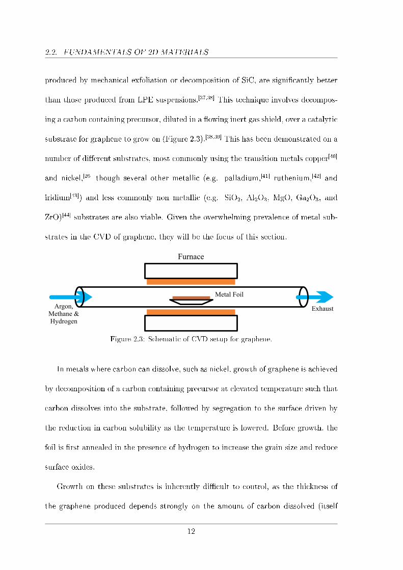
than those produced from LPE suspensions.[37,38] This technique involves decompos-
ing a carbon containing precursor, diluted in a �owing inert gas shield, over a catalytic
substrate for graphene to grow on (Figure 2.3).[38,39] This has been demonstrated on a
number of di�erent substrates, most commonly using the transition metals copper[40]
and nickel,[26] though several other metallic (e.g. palladium,[41] ruthenium,[42] and
iridium[43]) and less commonly non metallic (e.g. SiO2, Al2O3, MgO, Ga2O3, and
ZrO)[44] substrates are also viable. Given the overwhelming prevalence of metal sub-
strates in the CVD of graphene, they will be the focus of this section.
Argon,Methane &Hydrogen
Exhaust
Metal Foil
Furnace
Figure 2.3: Schematic of CVD setup for graphene.
In metals where carbon can dissolve, such as nickel, growth of graphene is achieved
by decomposition of a carbon containing precursor at elevated temperature such that
carbon dissolves into the substrate, followed by segregation to the surface driven by
the reduction in carbon solubility as the temperature is lowered. Before growth, the
foil is �rst annealed in the presence of hydrogen to increase the grain size and reduce
surface oxides.
Growth on these substrates is inherently di�cult to control, as the thickness of
the graphene produced depends strongly on the amount of carbon dissolved (itself
12
2.2. FUNDAMENTALS OF 2D MATERIALS
a function of precursor pressure, exposure time, and foil thickness) and the cooling
rate.[23,45] High cooling rates result in too much carbon segregating to the surface,
producing thick graphitic layers; low cooling rates limit segregation to the surface
since carbon di�uses into the bulk, inhibiting growth. Similarly, very high cooling
rates prevent growth by quenching the substrate and preventing di�usion to the
surface.[46] Further complicating matters, carbon preferentially segregates to grain
boundaries, resulting in thicker graphene in these areas.[38]
A preferable substrate is one in which carbon has very low solubility, such as
copper. In this case, growth is achieved not by segregation but by adsorption onto
the substrate surface. As with nickel, the foil is annealed in the presence of hydrogen
before the carbon is supplied by decomposition of a precursor. Growth occurs when
there is su�cient saturation of carbon on the copper surface for nucleation to occur,
which will then grow and coalesce into a polycrystalline �lm provided there is su�cient
carbon supply.[38] Due to its low reactivity, copper requires growth temperatures of
over 1000 °C, but unlike nickel low pressure is not needed since there is no need to
prevent excess carbon dissolution.[47] Another advantage is that this process is largely
surface limited and therefore monolayer �lms are much more readily achievable, which
has meant that copper has largely superseded nickel.[38]
Though the surface-only process simpli�es growth somewhat, parameters must
still be carefully controlled: insu�cient supply of carbon will result in incomplete
coverage; excess supply leads to a large number of nuclei and so a �ne grained �lm, as
well as producing bilayer or thicker regions at the nucleation points.[47,48] To obtain
the highest quality �lms a balance must be found between these two extremes.[48]
13

2.2. FUNDAMENTALS OF 2D MATERIALS
Another factor is the quality of the copper foil, as nucleation is favoured on surface
imperfections such as roughness and grain boundaries. To limit nucleation, foils are
polished to reduce roughness,[49] and annealed prior to the precursor introduction to
encourage grain growth.[19,50]
14

2.2. FUNDAMENTALS OF 2D MATERIALS
2.2.2 Transition Metal Dichalcogenides
Chalcogen
Metal
Figure 2.4: General structure of 2H-transition metal dichalcogenides.
2.2.2.1 Properties
Transition metal dichalcogenides (TMDs) are a subset of the layered metal dichal-
cogenides, a large family of materials consisting of one metal atom to every two
chalcogen (group 16) atoms that can commonly be isolated into monolayer form.[7]
TMDs are the most extensively studied in this area, with properties ranging from
metallic to semiconducting depending on the crystal structure and transition metal
used.[3] This review will focus on those that are semiconducting, since they are most
pertinent to �exible electronics.
Within the study of semiconducting TMDs, the vast majority of work has been
performed on those based on molybdenum and tungsten, though there is evidence that
several others such as titanium, zirconium,[51] and tin[52] also display this behaviour.[3]
15
2.2. FUNDAMENTALS OF 2D MATERIALS
All of these materials have similar physical and electronic properties, so what follows
will be a general description based primarily on studies of W- and Mo-dichalcogenides.
Like graphene, TMDs are physically robust. MoS2 has been found to have a
Young's modulus of ∼270 GPa, breaking strength of ∼15 Nm-1,[53] and failure strains
up to 25 %.[54] As with other 2D materials they are highly transparent to visible
light, with absorption varying but typically less than 5 %, but unlike graphene some
wavelengths will be more strongly attenuated due to bandgap absorption.[55,56]
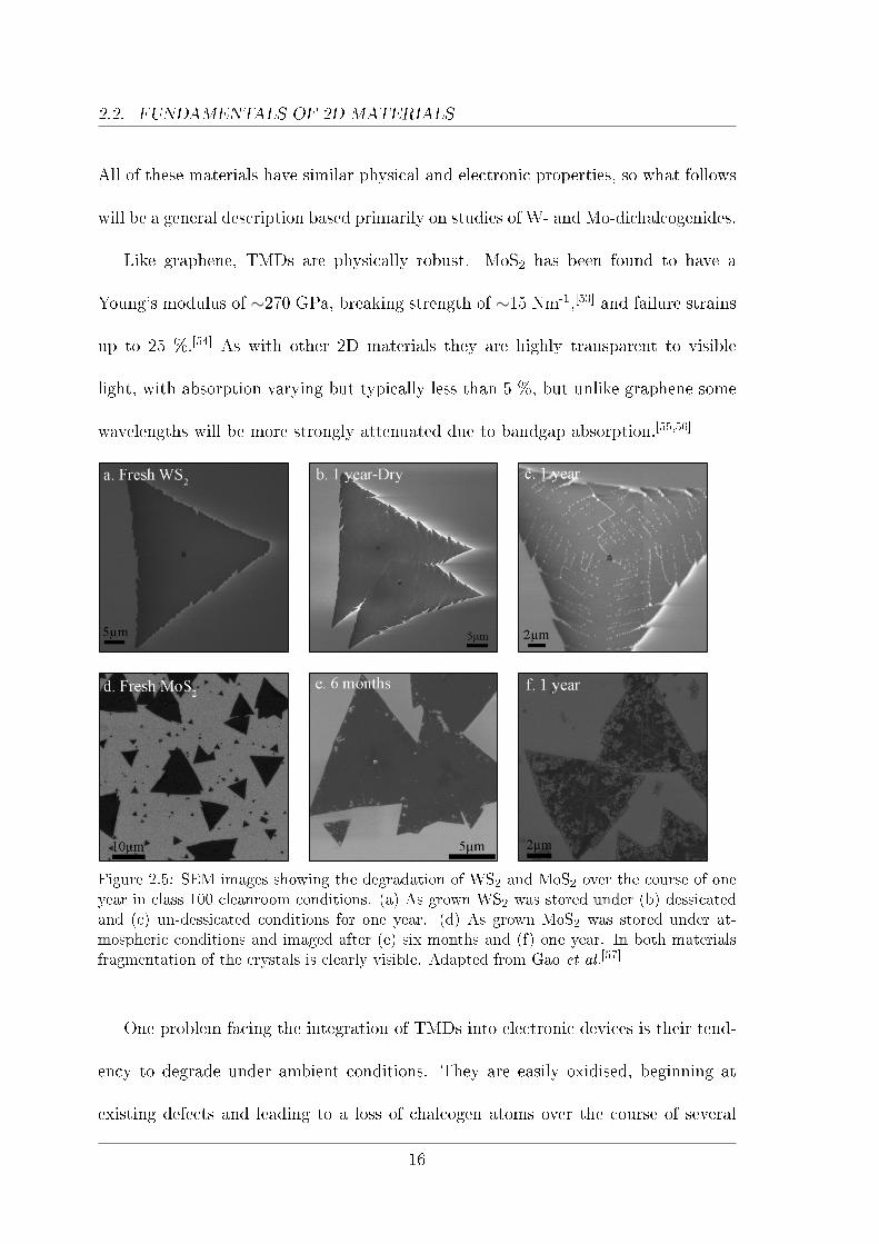
Figure 2.5: SEM images showing the degradation of WS2 and MoS2 over the course of oneyear in class 100 cleanroom conditions. (a) As grown WS2 was stored under (b) dessicatedand (c) un-dessicated conditions for one year. (d) As grown MoS2 was stored under at-mospheric conditions and imaged after (e) six months and (f) one year. In both materialsfragmentation of the crystals is clearly visible. Adapted from Gao et al.[57]
One problem facing the integration of TMDs into electronic devices is their tend-
ency to degrade under ambient conditions. They are easily oxidised, beginning at
existing defects and leading to a loss of chalcogen atoms over the course of several
16

2.2. FUNDAMENTALS OF 2D MATERIALS
months as they are substituted for oxygen.[57,58] This e�ect can also be mediated
by photoexcitation,[59] and electronic biasing.[60] Figure 2.5 shows the e�ects of such
degradation on WS2 and MoS2. The resultant fragmentation of the crystals and
breakdown of electronic properties will necessitate strategies to inhibit this e�ect and
ensure stable device performance over long periods. Graphene had been shown to in-
hibit the oxidation when placed beneath WS2, by screening the surface electric �elds
around the initiating defects.[58] Encapsulation with hBN is another viable strategy
to inhibit degradation.[59]
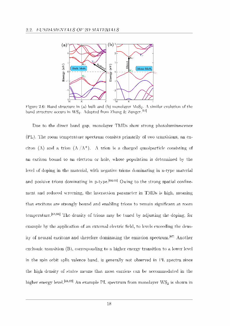
In monolayer form, these materials are direct band gap semiconductors (in the 2H
co-ordination shown in Figure 2.4; the 1T co-ordination leads to metallic behaviour
but is commonly less stable[14]) with gaps that range from visible to near-infrared,
decreasing with increasing chalcogen atomic mass.[19] This direct band gap develops
from the indirect gap of the bulk due to a combination of quantum con�nement and
loss of interlayer coupling, raising the energy of the TC point and lowering the energy
of the ΓV point until the gap shifts from the ΓV�TC transition of the bulk, to an in-
termediate ΓV�KC for 2�4 layers and �nally to KV�KC in monolayer (Figure 2.6).[61]
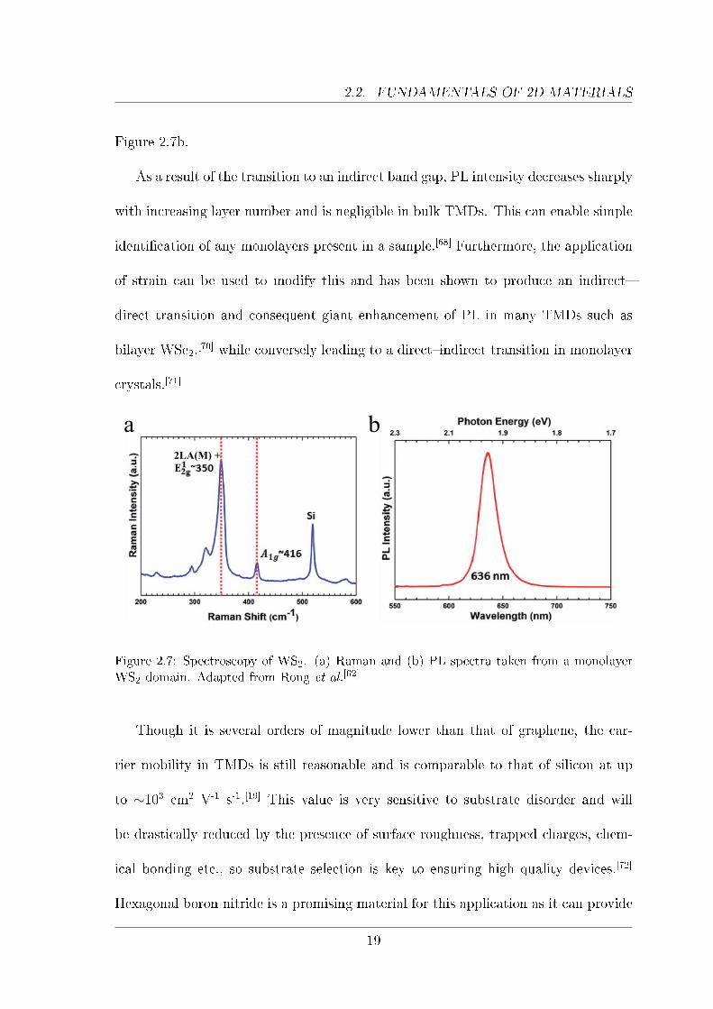
The Raman spectra of TMDs has two characteristic peaks that are also indicative
of the number of layers present, the E12g and the A1g. The E1
2g/A1g intensity ratio
is >3 in monolayer, decreasing to ∼2 in bilayer and decreasing further in thicker
�akes.[62,63] An example of the Raman spectrum of monolayer of WS2 is provided in
Figure 2.7a. Due to the excitation wavelength of 532 nm used, here there is also a
secondary acoustic mode (2LA(M)) centred at approximately the same shift as the
E12g�individual contributions may be revealed by Lorentzian �tting.
17
2.2. FUNDAMENTALS OF 2D MATERIALS
Figure 2.6: Band structure in (a) bulk and (b) monolayer MoS2. A similar evolution of theband structure occurs in WS2. Adapted from Zhang & Zunger.[61]
Due to the direct band gap, monolayer TMDs show strong photoluminescence
(PL). The room temperature spectrum consists primarily of two transitions, an ex-
citon (A) and a trion (A-/A+). A trion is a charged quasiparticle consisting of
an exciton bound to an electron or hole, whose population is determined by the
level of doping in the material, with negative trions dominating in n-type material
and positive trions dominating in p-type.[64,65] Owing to the strong spatial con�ne-
ment and reduced screening, the interaction parameter in TMDs is high, meaning
that excitons are strongly bound and enabling trions to remain signi�cant at room
temperature.[64,66] The density of trions may be tuned by adjusting the doping, for
example by the application of an external electric �eld, to levels exceeding the dens-
ity of neutral excitons and therefore dominating the emission spectrum.[67] Another
excitonic transition (B), corresponding to a higher energy transition to a lower level
in the spin-orbit split valence band, is generally not observed in PL spectra since
the high density of states means that most carriers can be accommodated in the
higher energy level.[68,69] An example PL spectrum from monolayer WS2 is shown in
18
2.2. FUNDAMENTALS OF 2D MATERIALS
Figure 2.7b.
As a result of the transition to an indirect band gap, PL intensity decreases sharply
with increasing layer number and is negligible in bulk TMDs. This can enable simple
identi�cation of any monolayers present in a sample.[68] Furthermore, the application
of strain can be used to modify this and has been shown to produce an indirect�
direct transition and consequent giant enhancement of PL in many TMDs such as
bilayer WSe2,[70] while conversely leading to a direct�indirect transition in monolayer
crystals.[71]
a b
2LA(M) +
Figure 2.7: Spectroscopy of WS2. (a) Raman and (b) PL spectra taken from a monolayerWS2 domain. Adapted from Rong et al.[62]
Though it is several orders of magnitude lower than that of graphene, the car-
rier mobility in TMDs is still reasonable and is comparable to that of silicon at up
to ∼103 cm2 V-1 s-1.[19] This value is very sensitive to substrate disorder and will
be drastically reduced by the presence of surface roughness, trapped charges, chem-
ical bonding etc., so substrate selection is key to ensuring high quality devices.[72]
Hexagonal boron nitride is a promising material for this application as it can provide
19

2.2. FUNDAMENTALS OF 2D MATERIALS
good surface �atness and high dielectric screening of the underlying substrate, thereby
acting to increase carrier mobility.[73,74]
2.2.2.2 Synthesis
Like graphene, synthesis of free monolayer TMDs was initially achieved by mechanical
exfoliation, a process which produces high quality �akes but is severely limited in the
scale of the crystals it can produce.[75] Preparation of liquid phase solutions has been
possible since the 1980s, most e�ectively by intercalation of lithium ions between
layers in bulk TMD crystals, followed by exposure to water so that the lithium reacts
and produces hydrogen gas that pushes the layers apart.[76] This technique has the
disadvantage of causing a phase change to 1T, changing the behaviour to metallic
and requiring annealing to restore the 2H structure.[77] LPE is also possible without
intercalation�for example by using ultrasonication�but the yield of monolayer �akes
is comparatively poor.[78] The suspensions can then be processed into �lms, but their
usefulness is hampered by their low quality.[79,80] Driven by the need for higher quality
�lms and encouraged by successes in the synthesis of graphene, there has been a large
amount of research into growing TMDs by CVD.[80,81]
CVD of these materials is complicated by the fact that they are composed of two
elements, and that these elements do not typically have suitable gaseous precursors
since those that exist are usually highly hazardous and require complex handling.[82,83]
The di�culties are further compounded by the fact that unlike the surface limited
growth of graphene on copper where the formation of monolayers is favoured, TMDs
have a propensity to form multilayers,[84] nanoparticles, or wires.[62,85,86] In spite of
20
2.2. FUNDAMENTALS OF 2D MATERIALS
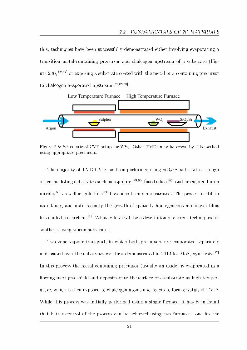
this, techniques have been successfully demonstrated either involving evaporating a
transition metal-containing precursor and chalcogen upstream of a substrate (Fig-
ure 2.8),[62,87] or exposing a substrate coated with the metal or a containing precursor
to chalcogen evaporated upstream.[82,88,89]
Argon Exhaust
Sulphur WO3 SiO2/Si
Low Temperature Furnace High Temperature Furnace
Figure 2.8: Schematic of CVD setup for WS2. Other TMDs may be grown by this methodusing appropriate precursors.
The majority of TMD CVD has been performed using SiO2/Si substrates, though
other insulating substrates such as sapphire,[88,90] fused silica,[82] and hexagonal boron
nitride,[91] as well as gold foils[83] have also been demonstrated. The process is still in
its infancy, and until recently the growth of spatially homogeneous monolayer �lms
has eluded researchers.[82] What follows will be a description of current techniques for
synthesis using silicon substrates.
Two zone vapour transport, in which both precursors are evaporated separately
and passed over the substrate, was �rst demonstrated in 2012 for MoS2 synthesis.[87]
In this process the metal containing precursor (usually an oxide) is evaporated in a
�owing inert gas shield and deposits onto the surface of a substrate at high temper-
ature, which is then exposed to chalcogen atoms and reacts to form crystals of TMD.
While this process was initially performed using a single furnace, it has been found
that better control of the process can be achieved using two furnaces�one for the
21

2.2. FUNDAMENTALS OF 2D MATERIALS
chalcogen and one for the metal precursor and substrate.[62,87] Using this technique
large triangular domains have been demonstrated up to several hundred microns in
size, though coverage is in general inhomogeneous, with high density toward the centre
of the substrate and sparse coverage at the edges.[62] Nucleation can be seeded, com-
monly using graphene derivatives such as reduced graphene oxide (rGO),[87] but this
will result in degraded electronic properties due to impurities in the �nal �lm and a
�ner grain structure, so is not favoured.[83]
An alternative method involves coating the substrate with the metal precursor
and sulphur/selen/tellur-ising it at elevated temperature under inert gas shield. This
process is similar to the two zone vapour transport method but has the potential to
more reliably provide complete coverage if a homogeneous distribution of the metal
precursor can be achieved. As for two zone vapour transport it was �rst demonstrated
in 2012 for MoS2 synthesis, using electron beam evaporation of Mo metal[89] or a
solution of (NH4)2MoS4,[88] followed by sulphurisation at high temperature. Some
monolayer regions were observed for the metal coated substrate but in general thicker
material was produced, rendering this process unsuitable for large scale monolayer
production.[88,89]
Recent work has shown that it is possible to grow continuous monolayer �lms.
Gold foils have been shown to be suitable catalysts for monolayer growth by a sur-
face mediated process, and �lms have been grown with grain sizes up to 420 μm,
using ammonium metatungstate and H2S.[83] Another technique used molybdenum
or tungsten hexacarbonyl (both highly toxic gaseous precursors) and (C2H5)2S at low
pressure to grow 4 inch �lms on fused silica substrates by controlling the precursor
22

2.2. FUNDAMENTALS OF 2D MATERIALS
supply so that edge attachment was favoured, but the grain size was limited to mi-
cron scale, with a maximum size of ∼15 μm.[82] Larger crystals have still more recently
been demonstrated using both CVD growth and decomposition growth on sapphire
substrates.[92]
23

2.2. FUNDAMENTALS OF 2D MATERIALS
2.2.3 Hexagonal Boron Nitride
Nitrogen
Boron
Figure 2.9: Structure of hexagonal boron nitride.
2.2.3.1 Properties
Hexagonal boron nitride (hBN) is a material that is structurally very similar to
graphene, with the carbon atoms replaced alternately by boron and nitrogen atoms,
as shown in Figure 2.9.[93] Though not as impressive as those of graphene, the mech-
anical properties of hBN are still very good, with a measured breaking strength of
15.7 Nm-1 and comparable sti�ness at up to 880 GPa.[11,93,94] The lattice parameter of
hBN closely matches that of graphene, di�ering by around 2 %.[94] So far the fracture
strain has lagged behind the theoretical value of 24 % with measured values of 3�4 %,
but this may be an issue of material quality as others such as graphene and MoS2
have both been shown to have good agreement between measurement and theory.[11]
Despite its structural similarities, in its electronic properties hBN di�ers greatly
24

2.2. FUNDAMENTALS OF 2D MATERIALS
from graphene: it is an insulator with a wide band gap of 6 eV and high electrical
resistance.[95] The dielectric constant decreases as it is thinned down to monolayer but
is still high at 2.31, 2.43, and 2.49 for mono-, bi-, and trilayer �lms respectively.[96]
This has lead to interest in its use as a complementary material for metal-insulator[94]
and other device applications in conjunction with other 2D materials.[96]
hBN has even lower optical absorption than graphene, with broadband visible
absorption at <1 %, and stronger absorption beginning at 202 nm due to excitation
of carriers across the bandgap.[94,97] The Raman signal of hBN shows a single charac-
teristic peak analogous to the G peak in graphene at ∼1366 cm-1 for bulk material
that blueshifts up to ∼1368 cm-1 in bilayer and ∼1370 cm-1 in monolayer, as shown
in Figure 2.10.[98]
a b
Figure 2.10: �(a) Raman spectra of atomically thin hBN. The left inset show changes inintegrated intensity IT with the number of layers N. The right picture illustrates the phononmode responsible for the Raman peak. (b) Position of the Raman peak for di�erent values ofN. In mono- and bilayer hBN, the peak position is sample-dependent and varies by as muchas ±2 cm=1. The dashed line is the Raman shift predicted for monolayer hBN, compared tothe bulk value (grey bar). The error bar indicates the typical accuracy of determining thepeak position using our spectrometer.� Adapted from Gorbachev et al.[98]
25
2.2. FUNDAMENTALS OF 2D MATERIALS
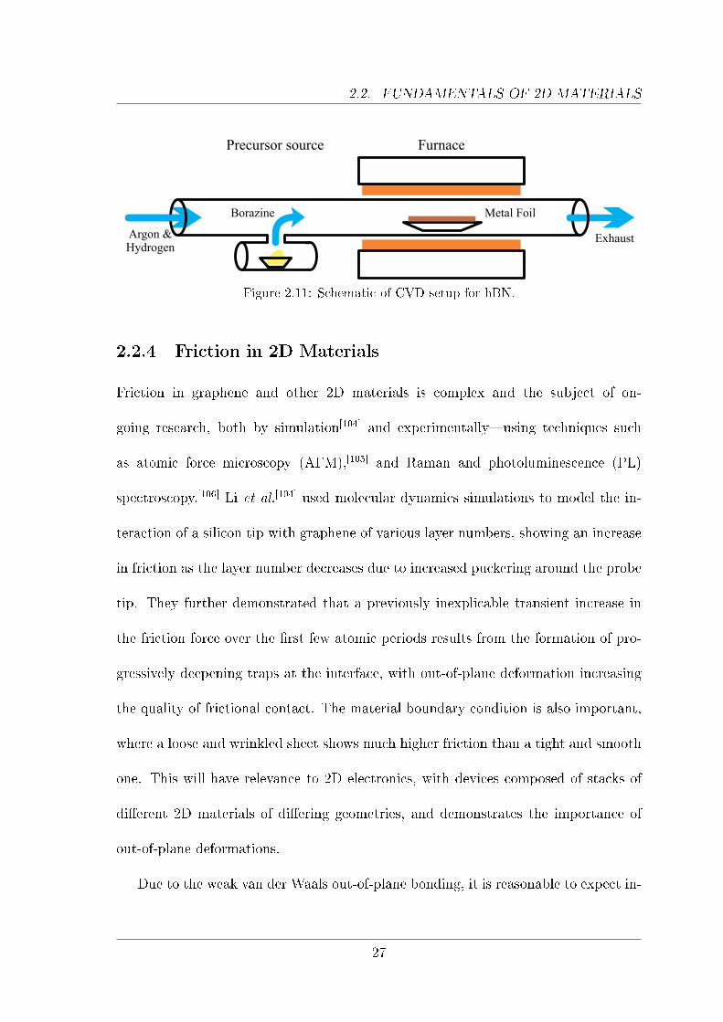
2.2.3.2 Synthesis
Once again, synthesis of monolayer hBN was �rst achieved by mechanical exfoliation.[75]
Liquid phase exfoliation can also be performed.[97] Both of these techniques still su�er
from the problems outlined for graphene in Section 2.2.1.2.
CVD has been demonstrated to be an e�ective technique for producing thin �lms
of hBN, using a process very similar to graphene.[94] Catalytic substrates such as
copper,[93,94] nickel,[99] and platinum[100] have been successfully employed to produce
�lms with full coverage over the substrate, but control over this process is less well un-
derstood and the �lms produced are typically �ne grained structures of mono- to few-
layer material.[94] Recent developments using electropolished copper substrates have
had some success at replicating the advances in the CVD of graphene, with continuous
monolayer �lms synthesised with grain sizes up to ∼35 μm.[94] A number of di�erent
precursors have been employed, in general solids such as polymeric aminoborane[94] or
ammonia borane, which are thermally decomposed to release borazine,[100] or indeed
liquids such as borazine itself.[99] Earlier work often used high vacuum,[101,102] but
most recent work has focussed on ambient pressure synthesis.[94,100] Chang et al.[103]
recently demonstrated that the growth morphology could be coarsened by limiting
nucleation through controlled passivation of the copper growth substrate by means
of an oxide layer. In all cases the process in general involves the decomposition of a
precursor by heating in a �owing inert gas shield in the presence of hydrogen, which
then passes over the substrate so that a �lm is deposited (cf. CVD of graphene,
Section 2.2.1.2).[94] A schematic of the typical CVD setup is shown in Figure 2.11.
26
2.2. FUNDAMENTALS OF 2D MATERIALS
Argon &Hydrogen
Exhaust
Metal Foil
Furnace
Borazine
Precursor source
Figure 2.11: Schematic of CVD setup for hBN.
2.2.4 Friction in 2D Materials
Friction in graphene and other 2D materials is complex and the subject of on-
going research, both by simulation[104] and experimentally�using techniques such
as atomic force microscopy (AFM),[105] and Raman and photoluminescence (PL)
spectroscopy.[106] Li et al.[104] used molecular dynamics simulations to model the in-
teraction of a silicon tip with graphene of various layer numbers, showing an increase
in friction as the layer number decreases due to increased puckering around the probe
tip. They further demonstrated that a previously inexplicable transient increase in
the friction force over the �rst few atomic periods results from the formation of pro-
gressively deepening traps at the interface, with out-of-plane deformation increasing
the quality of frictional contact. The material boundary condition is also important,
where a loose and wrinkled sheet shows much higher friction than a tight and smooth
one. This will have relevance to 2D electronics, with devices composed of stacks of
di�erent 2D materials of di�ering geometries, and demonstrates the importance of
out-of-plane deformations.
Due to the weak van der Waals out-of-plane bonding, it is reasonable to expect in-
27

2.2. FUNDAMENTALS OF 2D MATERIALS
complete transfer of strain from the substrate to the 2D materials.[107�110] Liu et al.[106]
used Raman and PL mapping to study the distribution of strain within triangular
domains of monolayer MoS2 on strained polydimethylsiloxane (PDMS) substrates,
�nding that at higher strains only ∼10 % of strain is transferred, and that trans-
ferred strain propagates through the triangle beginning at the point aligned most
closely with the strain axis. Though incomplete strain transfer has previously been
observed in 2D materials on soft substrates under tension, with the well documented
impact of strain �elds and inhomogeneities on 2D materials there is signi�cant scope
for improvement in the description of the mechanism and its in�uence on di�erent
heterostructures.[111,112]
28
2.3. DEVICES
2.3 Devices
Although it will be di�cult for heterostructured devices composed of these materials
to compete with the well-established semiconductors such as silicon and III-Vs in
established high-performance applications,[11] many novel device designs have now
been produced with interesting and sometimes unique properties.[20,113�115] One area
in which they compare more favourably is in �exible and/or transparent electronics,
with comparable strain resilience[3,11,19] and optical transmissivity,[8,116] and carrier
mobilities often far exceeding those of competing technologies such as conducting
polymers.[11]
The local environment can strongly in�uence the properties of 2D materials due to
their high speci�c surface area;[117,118] this typically manifests as changes to the doping
level or bandgap,[118�121] but can also lead to shifts in work function and strain.[122]
For this reason, it is necessary to have an understanding of the interactions between
2D materials in heterostructures. The �eld of �exible electronics provides a further
complication in the form of strain, which can again cause changes to the bandgap
and modify the interactions between the di�erent materials.[16,107,123�126]
As we have already touched upon, in recent years there has been considerable
interest in the use of 2D materials in �exible electronics. There have been a great
many demonstrations of devices composed of graphene, as well as heterostructure
devices making use of a wide range of di�erent 2D materials; however to date the
realisation of on chip fabrication using scalable processes has typically remained out-
side the scope of the majority of work, which has focused instead on small scale
29

2.3. DEVICES
proofs of concept.[14,37,92,127�130] There has also been extensive research into the de-
position of liquid phase exfoliated material in the form of inkjet[131,132] or otherwise
printed devices,[19,37,79,131�136] but limited research into devices composed of the large
area, high quality materials obtainable by CVD. As such, more research is needed
into the fabrication techniques for producing devices using scalable methods, and the
characterisation of their properties, particularly during the application of strain.
There are signi�cant limitations placed on the possible fabrication and processing
techniques when using polymeric substrates. This is due to their typically lower
thermal and chemical stabilities and, in contrast to silicon (SiO2/Si) wafers speci�c-
ally, their lack of conductivity and intrinsic back gate. For this reason, it is necessary
to modify the conventional methods for truly scalable production, i.e. complete on
chip fabrication, without electron beam lithography.[137�139] The impressive properties
of the materials described above can only be realised in real world applications by
combining them together into devices. This section will outline current work in this
area, concentrating on studies of �exible electronics, as well as technologies demon-
strated on rigid substrates that may be suitable in this application.
2.3.1 Advantages of 2D Materials
There are a number of factors that make 2D materials attractive candidates for �ex-
ible electronics. Foremost, there are clear advantages in the electronic properties,
especially carrier mobility. This is a parameter which has severely hampered imple-
mentation of high performance devices, since it has lagged behind conventional rigid
material performance signi�cantly.[37] Especially in the case of graphene but also�and
30
2.3. DEVICES
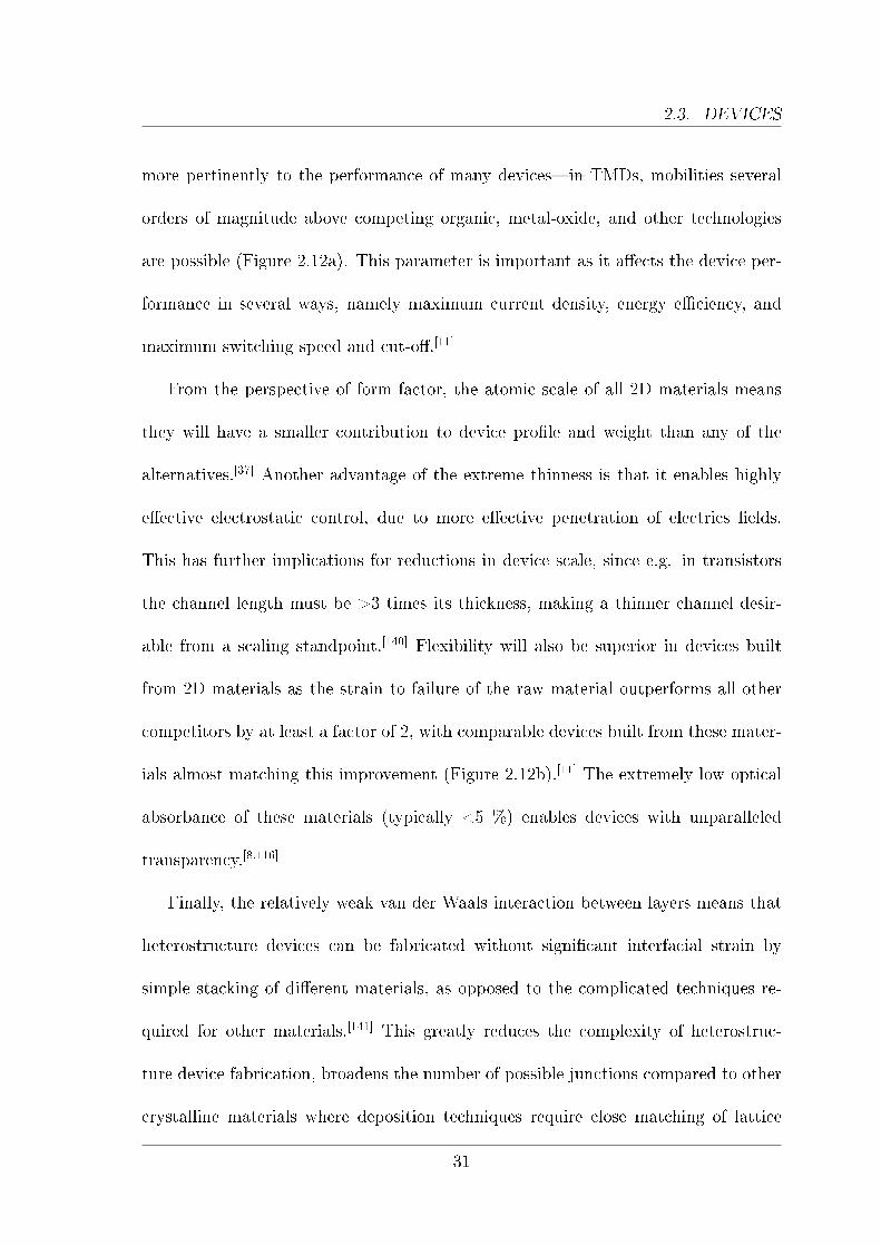
more pertinently to the performance of many devices�in TMDs, mobilities several
orders of magnitude above competing organic, metal-oxide, and other technologies
are possible (Figure 2.12a). This parameter is important as it a�ects the device per-
formance in several ways, namely maximum current density, energy e�ciency, and
maximum switching speed and cut-o�.[11]
From the perspective of form factor, the atomic scale of all 2D materials means
they will have a smaller contribution to device pro�le and weight than any of the
alternatives.[37] Another advantage of the extreme thinness is that it enables highly
e�ective electrostatic control, due to more e�ective penetration of electrics �elds.
This has further implications for reductions in device scale, since e.g. in transistors
the channel length must be >3 times its thickness, making a thinner channel desir-
able from a scaling standpoint.[140] Flexibility will also be superior in devices built
from 2D materials as the strain to failure of the raw material outperforms all other
competitors by at least a factor of 2, with comparable devices built from these mater-
ials almost matching this improvement (Figure 2.12b).[11] The extremely low optical
absorbance of these materials (typically <5 %) enables devices with unparalleled
transparency.[8,116]
Finally, the relatively weak van der Waals interaction between layers means that
heterostructure devices can be fabricated without signi�cant interfacial strain by
simple stacking of di�erent materials, as opposed to the complicated techniques re-
quired for other materials.[141] This greatly reduces the complexity of heterostruc-
ture device fabrication, broadens the number of possible junctions compared to other
crystalline materials where deposition techniques require close matching of lattice
31
2.3. DEVICES
a b
Figure 2.12: Comparison of the (a) mobilities and (b) strain limits of competing thin �lmmaterials. Adapted from Akinwande et al.[11]
parameters,[3] and completely removes the problem of interfacial mixing commonly
observed in organics.[142] In addition, the ease of out-of-plane deformations allows
arbitrarily stacked layers a high degree of conformation with underlying features.[3,23]
2.3.2 Issues & Challenges
Despite the numerous advantages outlined above, there are a number of problems
which must be overcome before wide scale adoption is possible. Though it is not
limited to 2D materials, heat dispersion is a challenge in thin �lm �exible electronics
due to poor thermal conductivity and lower maximum operating temperatures of
the polymer substrate materials, and is most pronounced in 2D devices due to the
high current densities required.[11] Studies of graphene show that Joule heating can
lead to peak temperatures in excess of 300 °C,[143] which is high enough to damage
most substrate materials, for example exceeding the glass transition temperature of
poly(ethylene terephthalate) (PET),[144] poly(ethylene naphthalate) (PEN),[145] and
poly(ether sulphone) (PES), and above the operating temperatures of others such as
polyimide (PI).[37]
32

2.3. DEVICES
Typical thermal management strategies in conventional electronics involve the use
of a metallic heat sink with large surface area to e�ciently transfer heat to the air, but
this is clearly not suitable in �exible electronics, and there is little research into heat
management strategies in this area.[11] Lee et al.[146] suggested an elegant strategy in
which the anisotropic thermal conductivity of a multilayer hBN �lm is exploited to
form an e�cient heat spreader, with the low out-of-plane conductivity limiting heat
transfer into the substrate and the high in-plane conductivity dispersing the heat over
a wide area. This combined with the aforementioned property of hBN to enhance
carrier mobility when employed as a substrate for other 2D materials make it a very
attractive material in this application.[74,147]
A related issue to the thermal management problem is device fabrication. Many
fabrication processes involve annealing steps to clean surface adsorbates[23,148] and
transfer sca�old residues,[8,149,150] or increase conformation of stacked layers[22] to im-
prove device quality, using temperatures that again exceed the operating temperatures
of most polymer substrates. The decreased carrier mobility and general lower quality
of �exible devices as compared to their rigid-substrate counterparts can partially be
explained by this limitation.[8]
There have recently been some developments in overcoming these problems us-
ing alternative strategies. Wood et al.[149] explored alternative polymer materials to
replace the de rigueur poly(methyl methacrylate) (PMMA) sca�old, and found that
polycarbonate sca�olds could be removed using room temperature chloroform to pro-
duce an �atomically-clean� surface. It should be noted that the use of chloroform
may preclude the use of some substrates.[151] For the removal of surface adsorbates,
33

2.3. DEVICES
Ovchinnikov et al.[152] used vacuum annealing at pressures down to 5 × 10⁻⁷ mbar at
a milder temperature of 115 °C to clean a WS2 transistor and found that mobility
increased by an order of magnitude, and on/o� ratio increased by nearly two. This
technique would be suitable for the more thermally stable substrates such as PEN
and PI.[37]
2.3.3 Device Designs
2.3.3.1 Transistors
Shortly after the discovery of graphene it was widely hoped that it could be utilised
in transistors, as its high carrier mobility would enable very fast devices. However,
progress has been hampered by its lack of an intrinsic band gap, and the complicated
methods required to create one of useful magnitude�such as physical con�nement to
nanoribbons,[17] or the application of strain[16,153,154]�meaning that such transistors
e�ectively cannot be switched o�.[3] TMDs are much more suitable as their large
band gaps mean that a low o� current is possible, increasing the on/o� ratio.[3,14,19]
Another advantage is that the mobility is typically fairly similar for both electrons
and holes, which has implications for simplifying combined n- and p-type devices by
enabling symmetric device design.[14] The vast majority of TMD transistors have been
demonstrated using MoS2, but the other dichalcogenides of Mo and W have also been
used, among others.[14]
Flexible thin �lm �eld-e�ect transistors (FETs) were �rst demonstrated by Pu et
al.[128] in 2012 using multilayer MoS2 and ion gel dielectrics. In this work, built on
successes with exfoliated material using rigid substrates and ionic liquid dielectrics,[155]
34

2.3. DEVICES
trilayer �lms of MoS2 were grown by CVD and transferred onto PI substrates, with
nickel bonded gold electrodes and an ion gel gate deposited on top to produce an
electric double-layer transistor (EDLT). After correcting for capacitance between the
ion gel and the source and drain electrodes, the performance of this device was then
compared with an identical device fabricated on an SiO2/Si substrate (Figure 2.13a).
A band structure for this device is shown in Figure 2.13b. In the absence of gate bias,
current �ow is blocked by the Schottky barriers. A positive gate bias will decrease
the depletion region width and increase the Fermi level, leading to the formation of
Ohmic contacts and increased current �ow. Though performance of the device on
SiO2 was superior to the one on PI (μ = 12.5 cm2 V-1 s-1 vs. μ = 3.01 cm2 V-1 s-1,
on/o� ratio ∼105 vs. ∼103), the performance of the �exible device was encouraging.
Di�erences were attributed to interactions with the polymer substrate lowering the
quality of the MoS2. No obvious electrical degradation was observed when the PI
device was bent to a radius of curvature of 0.75 mm across the channel direction.[128]
There have been a number of advancements in this area, with graphene source
and drain contacts,[129] and graphene gate electrodes with a hBN dielectric layer[8]
demonstrated independently, and more recently in conjunction.[127] Various substrates
have been used, but typically PET or PEN are used due to their high chemical
and thermal stability.[8,127,129] Using exfoliated bilayer WSe2, Das et al.[127] fabricated
a device from all 2D materials that was ∼88 % transparent with mobility up to
45 cm2 V-1 s-1, and an on/o� ratio 107. The device characteristics were unaltered
by strains of up to 2%.[127] These properties are comparable to equivalent devices
fabricated on SiO2/Si substrates.[22]
35

2.3. DEVICES
Φbn
EF
Φbp
Au AuMoS2ba
Figure 2.13: (a) Optical image and schematic of ion gel gated MoS2 EDLT structure. Ad-apted from Pu et al.[128] (b) Band structure for this device.
Another device design utilises the ultra thin nature of these materials to produce
switching in a heterostructure by tuning the Fermi level at the heterointerface to
modulate the tunnelling probability through a narrow barrier, enabling an on/o�
ratio up to 106.[3] Initially fabricated on an SiO2/Si substrate that was used as the
back gate electrode, this tunnelling �eld-e�ect transistor (TFET) consists of two
graphene electrodes separated by an insulating layer of hBN or TMD (Figure 2.14).
It exploits the low density of states (DOS) in graphene to enable a large increase
in the Fermi energy (EF) in both electrodes for a given gate voltage, decreasing the
e�ective tunnel barrier height and increasing the tunnelling DOS.[156] This drastically
increases current �ow by simultaneously increasing both the tunnelling probability
and amount of thermionic emission over the barrier.[156,157]
TFETs have since been demonstrated on PET substrates by Georgiou et al.,[157]
using WS2 as the tunnel barrier, to produce devices that were insensitive to bending
up to the 5 % strain tested, and demonstrating very similar behaviour to equivalent
devices fabricated on silicon. One disadvantage was the use of the PET substrate as
the gate dielectric, limiting the electric �eld due to the large separation between gate
36
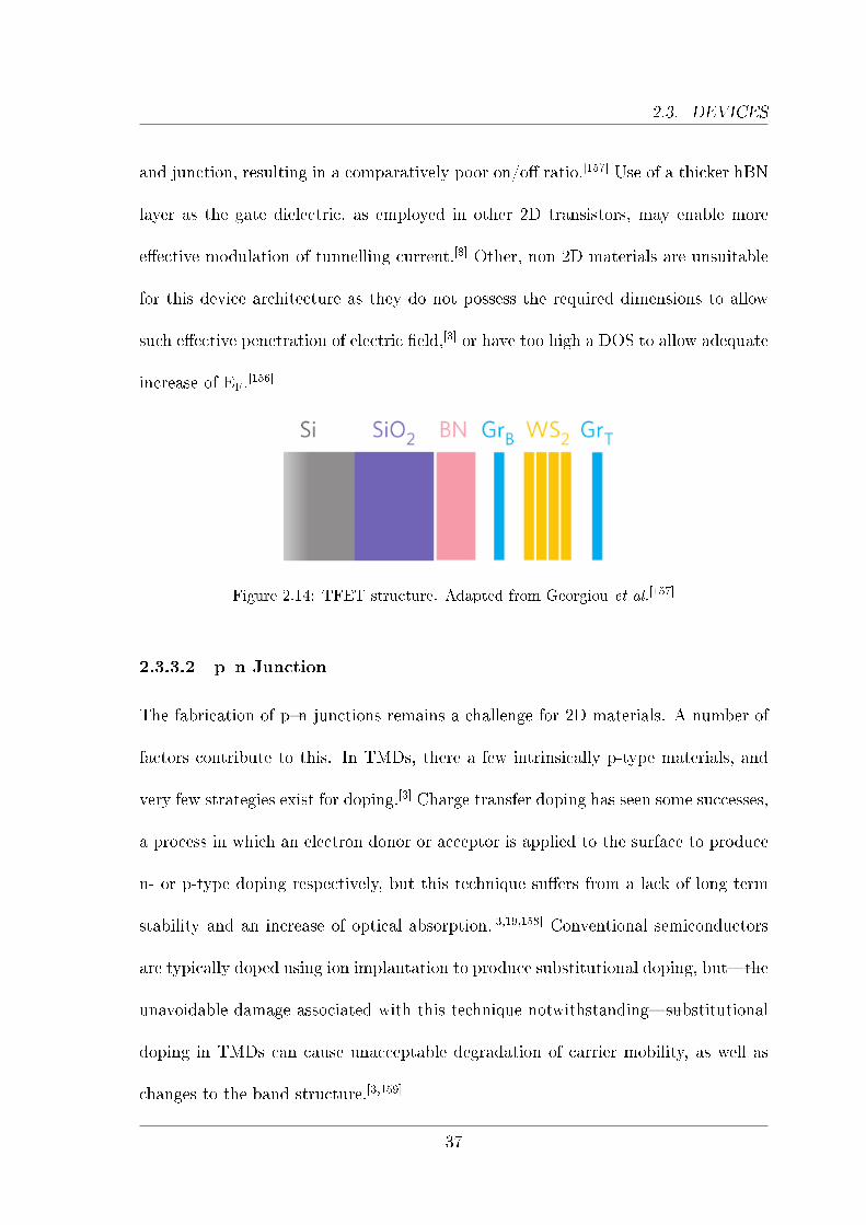
2.3. DEVICES
and junction, resulting in a comparatively poor on/o� ratio.[157] Use of a thicker hBN
layer as the gate dielectric, as employed in other 2D transistors, may enable more
e�ective modulation of tunnelling current.[8] Other, non 2D materials are unsuitable
for this device architecture as they do not possess the required dimensions to allow
such e�ective penetration of electric �eld,[3] or have too high a DOS to allow adequate
increase of EF.[156]
Figure 2.14: TFET structure. Adapted from Georgiou et al.[157]
2.3.3.2 p�n Junction
The fabrication of p�n junctions remains a challenge for 2D materials. A number of
factors contribute to this. In TMDs, there a few intrinsically p-type materials, and
very few strategies exist for doping.[3] Charge transfer doping has seen some successes,
a process in which an electron donor or acceptor is applied to the surface to produce
n- or p-type doping respectively, but this technique su�ers from a lack of long term
stability and an increase of optical absorption.[3,19,158] Conventional semiconductors
are typically doped using ion implantation to produce substitutional doping, but�the
unavoidable damage associated with this technique notwithstanding�substitutional
doping in TMDs can cause unacceptable degradation of carrier mobility, as well as
changes to the band structure.[3,159]
37
2.3. DEVICES
One strategy for producing p�n junctions that has enjoyed some success is to
produce a vertical heterojunction from an n-type TMD and a non 2D p-type semi-
conductor. Jariwala et al.[160] produced such a device using MoS2 and a �lm of
single-walled carbon nanotubes (SWCNT) that showed strongly rectifying behaviour
(forward-reverse current ratio of 104) using a silicon substrate, but this design could
equally be produced on �exible substrates given the resilience of CNT �lms to strain.[11]
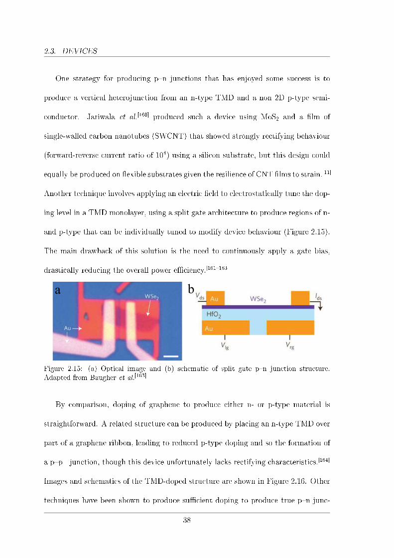
Another technique involves applying an electric �eld to electrostatically tune the dop-
ing level in a TMD monolayer, using a split gate architecture to produce regions of n-
and p-type that can be individually tuned to modify device behaviour (Figure 2.15).
The main drawback of this solution is the need to continuously apply a gate bias,
drastically reducing the overall power e�ciency.[161�163]
a b
Figure 2.15: (a) Optical image and (b) schematic of split gate p�n junction structure.Adapted from Baugher et al.[163]
By comparison, doping of graphene to produce either n- or p-type material is
straightforward. A related structure can be produced by placing an n-type TMD over
part of a graphene ribbon, leading to reduced p-type doping and so the formation of
a p�p+ junction, though this device unfortunately lacks rectifying characteristics.[164]
Images and schematics of the TMD-doped structure are shown in Figure 2.16. Other
techniques have been shown to produce su�cient doping to produce true p�n junc-
38

2.3. DEVICES
tions in graphene, using chemical doping, electrostatic gating, or optical gating via
photosensitive dye molecules.[165]
a b
c
d eGraphene/
WS2
Graphene
Ef
Figure 2.16: p�p+ junction produced by doping graphene using WS2. �(a) SEM image ofdevices with graphene channel and vertically stacked WS2 crystals. Bright square regionsare Cr/Au electrodes, which are used as source/drain contacts of the graphene FETs. Darktriangular domains are WS2 crystals. (b) SEM image with false color of the region indicatedin the blue dashed rectangle in panel a. (c) Side view schematic of device structure. (d) Topview optical image of the graphene FET device with WS2 partial coverage, with added coloroverlay to help identify the di�erent regions.� (e) �Schematic illustration of band structureof the two distinct graphene regions.� Adapted from Tan et al.[164]
2.3.3.3 Photodetectors
The operation of photodetectors depends on the excitation of carriers by incident
light, producing an increase in current �ow. The two main device designs exploiting
39
2.3. DEVICES
this principle are phototransistors and photodiodes, with the majority of 2D devices
studied so far being phototransistors.[3] With their direct band gaps in the visible to
near-infrared range TMDs are well suited in this application, with low dark current
ensured by Schottky barriers, and photogenerated excitons separated by a built in or
applied electric �eld to produce a signal.[3,19]
Metal�semiconductor�metal (MSM) geometries have been widely studied, with
early studies reporting that the photoresponse was dominated by the photothermo-
electric e�ect in which a temperature gradient resulting from absorbed photons gen-
erates a voltage across the metal-semiconductor junction due to di�ering Seebeck
coe�cients.[166] However, subsequent studies concluded that while this mechanism
contributes to the measured response, the dominant mechanism is still electric �eld
induced separation of excitons,[167] and a lowering of the Schottky barrier by the �lling
of trap states at the interface by photogenerated carriers.[168] Such devices generally
show internal ampli�cation of the photocurrent, leading to good responsivity that can
exceed 103 A W-1, but unfortunately response times (determined by the speed with
which carriers can be separated and collected by the source and drain electrodes) are
typically poor compared to photodiodes.[3] Hybrid devices which consist of graphene
on MoS2 have shown even greater responsivity (R >107 A W-1), with photoexcited
electrons injected into the graphene from the MoS2, while holes are blocked and act
to produce a positive gate voltage. The combination of these e�ects leads to a very
strong increase in conductivity.[169]
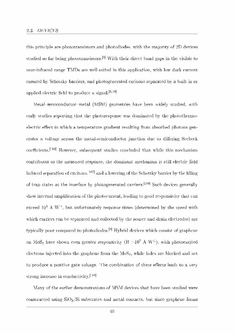
Many of the earlier demonstrations of MSM devices that have been studied were
constructed using SiO2/Si substrates and metal contacts, but since graphene forms
40

2.3. DEVICES
Schottky junctions with TMDs there is scope for producing �exible transparent
devices using the same principles.[170,171] A study by Hu et al.[172] compared the prop-
erties of Au contacted monolayer GaS (a related 2D semiconductor) on SiO2/Si and
PET substrates and found that PET increased responsivity by a factor of 4 (up
to ∼20 A W-1) while the response times remained similar at ≤30 ms (limited by
resolution of experimental setup). These values were found to decrease when the
�lms were bent, though this was attributed to a corresponding decrease in the ef-
fective irradiance of the device.[172] More recently there have been demonstrations of
devices utilising graphene electrodes, such as graphene�WS2�graphene,[121] graphene�
SnS2�graphene,[173] and graphene�WS2/MoS2�graphene.[174] The latter device showed
a signi�cant enhancement of 1�2 orders of magnitude in responsivity over equivalent
devices with isolated mono- or bilayers of either MoS2 or WS2, up to 1173 A W-1.[174]
Fabrication processes and schematics of the di�erent types of junction detailing the
di�erent con�gurations of monolayer and homo- or heterobilayers of TMDs are shown
in Figure 2.17.
The introduction of larger �elds to aid in exciton separation can dramatically
decrease response times and boost photoresponse. Lei et al.[175] demonstrated an
MSM avalanche photodetector based on monolayer InSe (another related 2D semi-
conductor), by using Al electrodes to produce Schottky junctions and applying a large
electric �eld to generate the avalanche e�ect. The high potential accelerates photo-
generated carriers to energies high enough to produce impact ionisation, generating
further excitons and consequent strong ampli�cation of the signal. The response
time of this device was 60 μs.[175] Another strategy to improve response times was
41
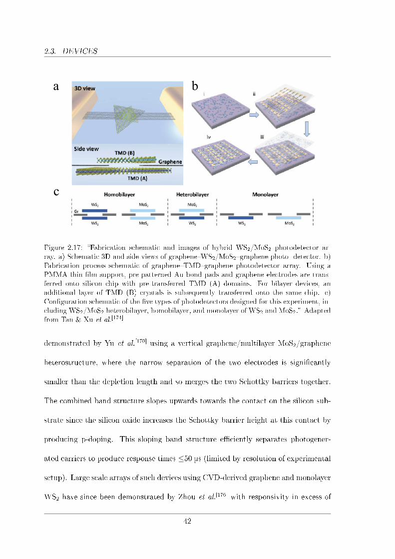
2.3. DEVICES
a b
c
Figure 2.17: �Fabrication schematic and images of hybrid WS2/MoS2 photodetector ar-ray. a) Schematic 3D and side views of graphene�WS2/MoS2�graphene photo- detector. b)Fabrication process schematic of graphene�TMD�graphene photodetector array. Using aPMMA thin-�lm support, pre-patterned Au bond pads and graphene electrodes are trans-ferred onto silicon chip with pre-transferred TMD (A) domains. For bilayer devices, anadditional layer of TMD (B) crystals is subsequently transferred onto the same chip. c)Con�guration schematic of the �ve types of photodetectors designed for this experiment, in-cluding WS2/MoS2 heterobilayer, homobilayer, and monolayer of WS2 and MoS2.� Adaptedfrom Tan & Xu et al.[174]
demonstrated by Yu et al.[170] using a vertical graphene/multilayer MoS2/graphene
heterostructure, where the narrow separation of the two electrodes is signi�cantly
smaller than the depletion length and so merges the two Schottky barriers together.
The combined band structure slopes upwards towards the contact on the silicon sub-
strate since the silicon oxide increases the Schottky barrier height at this contact by
producing p-doping. This sloping band structure e�ciently separates photogener-
ated carriers to produce response times ≤50 μs (limited by resolution of experimental
setup). Large scale arrays of such devices using CVD-derived graphene and monolayer
WS2 have since been demonstrated by Zhou et al.[176] with responsivity in excess of
42

2.3. DEVICES
103 A W-1.
Still faster response times may be achieved by using photodiodes. For example,
the previously described SWCNT�MoS2 p�n junctions show poorer responsivity of
around 0.1 A W-1, but have response times down to ≤15 μs.[160] The structure and
performance of such a device is detailed in Figure 2.18. Progress in producing all 2D
devices has again been limited by the di�culty of fabricating p�n junctions due to
the lack of techniques for stable doping of TMD �lms.[3]
2.3.3.4 Light-Emitting Diodes
As with photodiodes, the di�culty of producing p�n junctions has hampered devel-
opment of LEDs.[3] The aforementioned electrostatically doped devices were shown
to electroluminesce under bias, with WSe2 devices showing an external quantum e�-
ciency (EQE) up to ∼0.1 %.[161,162] This compares favourably to previous reports of
electroluminescence in MoS2 without an electrostatically produced p�n junction, in-
stead arising from impact ionisation across a Schottky barrier (EQE = 0.001 %),[177]
but is still far behind other �exible technologies.[141] Moreover, these devices were
only demonstrated on SiO2/Si substrates and may be di�cult to replicate on �exible
substrates due to the requirement of high applied gate voltage to induce the p�n
junction.[161�163]
A more e�ective approach has been facilitated by recent advances in heterostruc-
ture device fabrication, with early reports of devices with EQE approaching 10 %
from TMD �lms.[141] This compares favourably to organic LED (OLED) technology,
where EQEs are typically up to ∼15 %, a promising result considering the rate of
43
2.3. DEVICES
a b d
cMoS2
SWCNT
Ec
Ev
Ef
0 V -40 V
n p n-
p+
Figure 2.18: �Microscopy and fabrication of the s-SWCNTs/single layer (SL)-MoS2 p�n het-erojunction diode. (a) False coloured SEM image of the heterojunction diode. Scale bar2.5 μm. The yellow regions at the top and bottom are the gold electrodes. The patternedalumina (blue region) serves as a mask for insulating a portion of the SL-MoS2 �ake (violetregion). The pink region is the patterned random network of s-SWCNTs (p-type) in directcontact with the exposed part of the SL-MoS2 �ake (n-type) to form the p�n heterojunctiondiode (dark red). (b) Optical micrograph showing the device layout at a lower magni�cation.The dashed yellow boundary indicates the SL-MoS2 �ake, whereas the dashed white rect-angle denotes the patterned s-SWCNT �lm. Electrodes 1 and 2 form the n-type (SL-MoS2)FET, which is insulated by the patterned alumina �lm (cyan). Electrodes 2�3 form the p-nheterojunction, whereas 3�4 and 4�5 form p-type s-SWCNT FETs. Scale bar 10 μm.� (c)Band structures at a gate bias of 0 V (weakly rectifying behaviour) and �40 V (stronglyrectifying behaviour). �(d) Photodetection using the p�n heterojunction diode: the time-dependent photoresponse of the p�n heterojunction showing fast rise and decay times of∼15 μs.� Adapted from Jariwala et al.[160]
development of this nascent �eld, in contrast to the comparatively well developed
organic semiconductor industry.[141,178] The heterostructure devices, demonstrated by
Withers et al.[179] in 2015 using both SiO2 and PET substrates, consist of a mono-
layer TMD �lm bounded on each side by bi- or tri-layer hBN to produce a quantum
well (QW), which was then contacted by graphene and encapsulated in hBN (Fig-
ure 2.19a). The device luminescence arises from tunnelling of electrons and holes
44

2.3. DEVICES
through the hBN layers into the QW, producing excitons that rapidly recombine to
emit light due to the direct band gap (Figure 2.19b). This single QW device showed
an EQE of ∼1 %.
a b c
Figure 2.19: SQW LED structure and operation. (a) Ball-and-stick model. (b) Banddiagram of the LED under bias showing the injection of electrons and hole through the hBNinto the TMD, where they recombine to emit light. (c) Optical image of device in operationshowing red light emission. Scale bar 10 μm. Adapted from Wang & Xia.[141]
Improvements to the quantum e�ciency were achieved by stacking multiple extra
layers of the same hBN/TMD structure on top of one another to produce a multiple
QW structure, producing a maximum EQE of 8.4 %. Also fabricated were multiple
quantum wells using di�erent TMD materials, with the combination of a WSe2 and
MoS2 QW resulting in an increase to the EQE, up to ∼5 %. In this device light
originates from the WSe2 layer because its narrower band gap means that excitons
generated in the MoS2 �rst transfer to it before recombining. Importantly, the same
single QW devices were fabricated on PET substrates and showed equivalent lumin-
escence properties that did not vary up to the maximum measured strain of 1 %.[179]
hBN encapsulation has also enabled the formation of a thermal light emitter using
graphene, producing an ultrafast white light source with up 10 GHz bandwidth that
45

2.3. DEVICES
is stable up to electronic temperatures of 2000 K.[180]
2.3.3.5 Photovoltaics
Photovoltaic cells rely on the ability to e�ciently separate photogenerated excitons,
again typically requiring the creation of a p�n junction.[181] The di�culties posed by
this aside, TMDs are good candidates in this application since the Shockley�Queisser
limit calls for a high mobility semiconductor with a direct band gap of approximately
1.3 eV.[3] The split gate architecture used to produce p�n junctions has been shown
to have a power conversion e�ciency up to ∼0.5%, but the gating requirements make
this impractical.[162] A more e�cient device was shown using multilayer MoS2 con-
tacted in MSM geometry with one Au electrode and one Pd electrode (Figure 2.20a)
which, if used in isolation for both contacts, produce n- and p-type transport respect-
ively. This is due to a lowering of the Fermi energy at the Pd interface as compared
to the Au interface, in spite of their near identical work functions. The resulting
device shows asymmetric ambipolar transport and behaves as a diode (Figure 2.20b),
with the sloping band structure bounded by Schottky contacts (Figure 2.20c) e�ect-
ively separating photogenerated excitons to produce sizeable photocurrent with power
conversion e�ciency up to ∼2.5 %.[182]
Perovskite based photovoltaic devices have gained widespread interest as potential
low cost, thin �lm alternatives to silicon.[183,184] Single junction cells have developed
rapidly, with an increase in power conversion e�ciency (PCE) from 3.8 % to >22 %
over the last decade. Commonly produced with metallic thin �lm cathodes and
transparent anodes of indium tin oxide (ITO), �exible devices have been demonstrated
46

2.3. DEVICES
Figure 2.20: Photovoltaic device produced by asymmetric MSM geometry �(a) Optical imageof the device. The spacing between the electrodes is 2 mm. (b) Current vs. source-drainvoltage at VG= 0 showing strong asymmetry and photoresponse with diode-like behaviourfor the Pd-Au bias con�guration indicated in (a).� (c) Formation of sloping band structurethat leads to photovoltaic behaviour. Adapted from Fontana et al.[182]
with PCEs ranging typically from 10�17 %.[184] The recent demonstration of an all-
carbon-electrode device using CNT cathodes and graphene anodes by Luo et al.[184]
serves to highlight the advantages of replacement of the conventional with 1D and
2D materials, with PCE up to ∼12 % and enhanced stability and strain resilience
compared to ITO based devices.
Vertical heterostructures have again been exploited to give drastic improvements
in device e�ciency. Britnell et al.[181] produced a graphene/TMD/graphene stack
that had a built-in electric �eld produced by either the use of a back gate or p-doping
of the top contact using water vapour. Importantly, this �eld e�ectively separates
47

2.3. DEVICES
excitons generated in the full thickness and across the entire area of the few-layer
MoS2 used, which is an improvement over lateral devices where generation occurs
only in the comparatively small depletion regions. On SiO2/Si substrates, the devices
were found to have maximum EQEs in excess of 30 % at low laser power and using
a single frequency. This value declines as the laser power is increased, attributed to
screening of the built-in electric �eld due to the increasing concentration of carriers
in the MoS2.
In this geometry the photovoltaic e�ect appears to depend on the layer number,
with Zhou et al.[176] observing a photovoltaic e�ect in such devices (fabricated as de-
tailed in Figure 2.21) with bilayer WS2 but not in those with monolayer�attributed
to the longer lifetime of excitons and their smaller binding energy in bilayer material.
For PET substrates performance is more modest, due in part to poorer light ab-
sorption without the enhancement provided by the silicon substrate, with quantum
e�ciencies approximately halved to ∼15 %.[98,181] Enhanced EQEs (up to 55 %) have
been shown for devices using one graphene and one Ti contact, with a transparent
ITO gate electrode, but this device is not suitable for production with a �exible
substrate.[170]
2.3.3.6 Gas Sensors
By virtue of their unparalleled speci�c surface area, the adsorption of molecules can
strongly modulate the electrical conductivity by charge transfer. Using graphene,
such devices have been demonstrated to have sensitivities down to parts per billion
concentrations, most successfully using rGO,[12] but also with slightly lower sensitivity
48
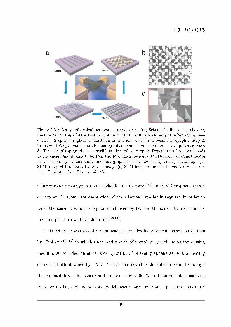
2.3. DEVICES
a b
c
Figure 2.21: Arrays of vertical heterostructure devices. �(a) Schematic illustration showingthe fabrication steps (Steps 1=4) for creating the vertically stacked graphene/WS2/graphenedevices. Step 1: Graphene nanoribbon fabrication by electron beam lithography. Step 2:Transfer of WS2 domains onto bottom graphene nanoribbons and removal of polymer. Step3: Transfer of top graphene nanoribbon electrodes. Step 4: Deposition of Au bond padsto graphene nanoribbons at bottom and top. Each device is isolated from all others beforemeasurement by cutting the connecting graphene electrodes using a sharp metal tip. (b)SEM image of the fabricated device array. (c) SEM image of one of the vertical devices in(b).� Reprinted from Zhou et al.[176]
using graphene foam grown on a nickel foam substrate,[185] and CVD graphene grown
on copper.[186] Complete desorption of the adsorbed species is required in order to
reuse the sensors, which is typically achieved by heating the sensor to a su�ciently
high temperature to drive them o�.[186,187]
This principle was recently demonstrated on �exible and transparent substrates
by Choi et al.,[187] in which they used a strip of monolayer graphene as the sensing
medium, surrounded on either side by strips of bilayer graphene as in situ heating
elements, both obtained by CVD. PES was employed as the substrate due to its high
thermal stability. This sensor had transparency > 90 %, and comparable sensitivity
to other CVD graphene sensors, which was nearly invariant up to the maximum
49

2.3. DEVICES
measured strain of 1.4 %. Sensitivity was good at ∼15 % for 1 part per million NO2,
and the integrated heater enabled recovery times down to ∼11 seconds.[187] Another
design developed by Kim et al.[188] uses trilayer graphene patterned into a 5 μm ribbon
that behaves as both the sensing medium and heating element, which showed similar
sensitivity but had signi�cantly longer recovery times, at a of minimum of 579 seconds.
Though graphene sensors natively lack selectivity, non-covalent functionalisation has
been used to specify the detection of particular molecules such as DNA, glucose, and
glutamate.[12]
TMDs have also been employed as gas sensors, in general again making use of
charge transfer from the adsorbed species. Similar sensitivities have been observed,
but TMDs have been shown to improve on one of the main drawbacks of graphene
gas sensors as they have higher selectivity without functionalisation.[3] For example,
single layer MoS2 has been found to be sensitive only to organic species that are
electron donating, with no signal observed for electron acceptors.[189] Guo et al.[190]
demonstrated a �exible humidity sensor using CVD-derived MoS2 in a palladium
contacted MSM geometry on PET. Applying tensile strain to this device by bending
leads to increased sensitivity by the piezotronic e�ect�a result of positive polarisation
charges lowering the Schottky barrier height.
Another mechanism for sensing is also possible with TMDs, making use of changes
to the photoluminescence or electroluminescence e�ciency, where electron acceptors
increase e�ciency in n-type material and decrease e�ciency in p-type. Demonstration
of this e�ect has been limited, but is promising due to the large magnitude of changes
possible, and corresponding high sensitivity.[191]
50

2.3. DEVICES
2.3.3.7 Strain Sensors
With their enormous resilience to strain, 2D materials are an obvious choice for strain
sensing applications.[27,54] A number of di�erent device designs have been proposed
to use graphene as the sensing medium, including plain �lms,[192,193] rippled �lms,[194]
foams,[195] and woven fabrics.[196] For plain �lms, there is some dispute over the mag-
nitude and mechanism of resistance change, with some reports of CVD �lms on PDMS
substrates showing almost no change in resistance with strain,[197] while others have
reported gauge factors ranging from the modest (∼0.4),[198] to the very large (up to
∼151), though in the latter case there was an initial region of almost no change up to
3 % strain.[193] The reasons for these di�erences are not well understood, but likely
result from variations in the preparation and transfer processes used, since this can
cause large di�erences in the quality of �lms due to grain boundaries, defects, and
damage. Another possible cause is damage during testing.[27]
A related design relies on the creation of ripples in the graphene �lm by the con-
trolled application of a tensile prestrain, that was relaxed after transfer. These ripples
increase the resistance of the �lm by causing increased scattering of carriers, and as
tensile strain is applied they relax and resistance falls (Figure 2.22). Though gauge
factors were modest at ∼=2, this has the the advantage of relying on a mechanism
that is more independent of �lm quality, as well as likely increasing the maximum
strain before non-recoverable deformation occurs.[27,194]
Graphene foams have been employed by breaking the foam down into fragments
and producing a �lm with overlapping fragments, producing gauge factors up to 29.
51

2.3. DEVICES
a b
Figure 2.22: Rippled graphene strain sensor. �(a) AFM image of the rippled (monolayer)graphene ribbons. (b) Resistance response of the rippled graphene device upon di�erentstrain. The insets are optical images before and after buckling; 20 % prestrain is used tocreate the rippled graphene device. The resistance decreases linearly from 5.9 kΩ to 3.6 kΩwhen the strain increases from 0 % to 20 %. The minimum resistance of 3.6 kΩ correspondsto the state of totally relaxed �at graphene.� Adapted from Zhao et al.[27]
The strain sensitivity was attributed to changes in the overlap of the fragments.
This device was shown to have excellent stability, withstanding strains up to 70 %
and showing consistent performance after 10000 cycles.[195] Graphene woven fabrics
embedded in PDMS show the largest gauge factors at ∼103 for small strains and
increasing to ∼106 for higher strains. This response is due to cracking of the fabric
producing a strong increase in resistance, up to a maximum usable strain of 15�20 %,
at which point no current can �ow. After initial fracturing, the response stabilises
and performance was found to be consistent over 100 cycles. However, due to the
destructive sensing mechanism, there may be problems with long term stability and
possible drift of unstrained resistance.[196]
There has also been limited research into producing strain sensors from TMDs.
Tsai et al.[199] produced FETs from trilayer MoS2 by etching channels and lithograph-
52

2.3. DEVICES
ically depositing gold contacts before transferring the devices onto PET substrates
with an ITO/Al2O3 back gate. Device performance was practically identical before
and after transfer. The device showed a gauge factor that was strongly dependent on
the magnitude of gate bias: approximately zero when it was in the o� state, increas-
ing to a maximum of ∼=40 in the subthreshold region, and decreasing again in the
linear regime. See Figure 2.23 for more details. This behaviour can be explained by
the piezoresistive e�ect, in which the strain decreases the magnitude of the bandgap,
and change of the Fermi level with gate voltage. In the o� state, changes to the band
gap have little impact on the conductivity as the device is switched o� regardless. In
the subthreshold region, the amount of carriers is strongly increased by reductions in
the bandgap. Finally, in the linear region the device is strongly conductive anyway,
so the reduced bandgap does not have such a signi�cant e�ect on the conductivity.
(f)
Figure 2.23: MoS2 strain sensor with gate modulated gauge factor. �(a) A top-view opticalimage of MoS2 FETs after fabrication on an SiO2=Si wafer. (b) A typical transistor with100 μm MoS2 channel length from the die in (a). (c) The released MoS2 FETs held with thePMMA layer �oating on water (the inset shows a higher magni�cation of the same �oatingsample). (d) A �exible transistor on the Al2O3/ITO/PET substrate with probes touchingthe source and drain contacts during electrical measurements. (e) Flexible MoS2 FETs ona transparent and �exible PET substrate covered with an ITO back-gate electrode and an80 nm Al2O3 dielectric layer.� (f) �The relationship between Δφn and Vbg of a representativedevice.� Adapted from Tsai et al.[199]
53

2.3. DEVICES
2.3.3.8 Cardio-Respiratory Monitor
To achieve stable, high resolution images in magnetic resonance imaging (MRI)
and computed tomography (CT) scanning and thereby minimise artefacts that may
lead to misdiagnosis or even mimic diseases, the e�ects of body motion must be
minimised.[200,201] This is achieved by monitoring the key sources of regular body
motion�the cardiac and respiratory cycles�and gating the image acquisition ac-
cordingly, wherein image data acquired during movement is either prospectively or,
less e�ciently, retrospectively discarded.[202�205]
In small animal imaging, so called respiratory balloons are de rigueur for respirat-
ory monitoring.[205�208] There are a number of variants of this device but all operate
on the same principle, as described by Herrmann et al.[209] and others. Respiratory
motion is monitored by a device that relies on the measurement of changes to air pres-
sure within a small pneumatic capsule, placed in contact with the the abdomen and
coupled to a pressure transducer.[205�208] Use of respiratory balloons requires careful
placement and calibration, and repressurisation is required if the animal is transferred
between systems�a major drawback in applications requiring co-registration between
di�erent scanning techniques, where changes to posture must be minimised.[210] Car-
diac gating is achieved by synchronisation to the electrocardiogram (ECG), commonly
by invasive subdermal needles,[205] though non-invasive means are also possible.[211,212]
Electrical measurement of the ECG can be problematic in the presence of MRI ima-
ging gradients.[211,213,214]
In response to issues with the respiratory balloons, piezoelectric sensors construc-
54

2.3. DEVICES
ted from poly(vinylidene �uoride) (PVDF) or a similar polymer and contacted by
metallic thin �lms were demonstrated in pre-clinical imaging as early as 1992 by
McKibben & Reo.[215] The advantage of the piezoelectric sensors lies with their com-
paratively simple setup and calibration, and their insensitivity to changes in air pres-
sure. However, they have not seen widespread adoption for the simple fact that
metallic �lms have signi�cant deleterious consequences for images produced by both
techniques. In MRI, all objects placed in the bore of the magnet lead to distortion and
detuning of the magnetic �eld, but metallic objects cause this e�ect most strongly due
to their high susceptibility, and when moved within the magnetic �eld can cause dis-
tortions to the image.[216,217] The radio waves used will also be strongly attenuated in
metallic objects, and the induced currents may lead to local heating and cause prob-
lems such as skin burns.[218] The presence of metal may also limit the magnitude of
magnetic �eld possible.[217] In CT imaging, the metal �lm is a strong X-ray scatterer,
blocking parts of the image from view and creating bright artefacts.[219�221]
As previously discussed, with its hexagonal lattice of sp2 bonded carbon graphene
is a material that uniquely combines high in-plane conductivity with extreme strain
resilience, whilst providing a negligible contribution to device sti�ness or pro�le.[26,27]
Unlike silver, graphene is radiolucent due to its extremely low scattering cross-section
and therefore will not be observed in CT imaging.[221] It is also suited for MRI applic-
ations for a number of reasons. Since carbon 12 (the predominant isotope of carbon)
has no net spin and consequently is not detected, the graphene lattice itself will only
be weakly imaged.[222] Despite its high magnetic susceptibility, the negligible volume
of graphene means it causes minimal distortion to the magnetic �eld.[223�225] Further-
55

2.3. DEVICES
more, several previous studies have identi�ed �ake edges as contributing chie�y to
the magnetism of graphene, and CVD derived material is a continuous �lm with the
minimum possible edge density for a given area (cf. �lms composed of liquid phase
exfoliated �akes of typically nm-μm size, each with associated edges and possible
consequent magnetic moments).[132,224,226]
The above properties combine to make make graphene highly attractive for use as
a planar conductor in MRI and CT imaging, since devices utilising it are likely to have
little to no impact on image acquisition. It is further suited to use in piezoelectric
sensors of this type as the signal is generated by de�ection, so the lower sti�ness
could increase device sensitivity, and the high strain resilience will increase device
durability.[27]
56
2.4. CONCLUSIONS
2.4 Conclusions
In this review, we have assessed the insulating, semiconducting, and metallic 2D
materials at the forefront of �exible electronics research, focusing on their relevant
physical, electronic, and optical properties, as well as examining the current state
of synthesis techniques. Though continuous polycrystalline �lms of reasonably good
quality have now been demonstrated for all of these materials, there is still much scope
for improvement in control over the grain size, layer number, and defect concentration,
especially in the case of TMDs.
The di�erent properties of these materials have great potential to be combined
synergistically in a wide range of devices. The nature of van der Waals bonding
provides the opportunity to produce heterostructured devices with atomically sharp
interfaces, without any of the complicated fabrication steps required for other ma-
terials. Due to their atomic thickness and associated extreme strain resilience, they
are well placed to provide alternatives in a multitude of applications. There are clear
advantages to using 2D materials in �exible electronic devices, often having greater
strain resilience, carrier mobility, and transparency than the existing alternatives,
among other factors.
In light of the above, a survey of current progress in the fabrication of �exible
electronic devices from 2D materials has been produced. The advantages and dis-
advantages have been outlined, along with the main device designs that have so far
been demonstrated and assessed. Where possible, this has been drawn from examples
where �exibility was already demonstrated, but in some cases relevant devices that
57
2.4. CONCLUSIONS
have thus far only been demonstrated on rigid substrates have also been explored.
The remainder of this thesis explores several of the areas described above, with im-
plications that reach beyond the speci�cs of each study to the wider �eld of �exible
electronics as a whole.
Research into these materials is still in its infancy, with the �rst isolation of
graphene in 2004, and other materials being discovered even more recently. Before
wide scale adoption into the semiconductor industry is possible there are many aspects
of synthesis, fabrication, and device design that require signi�cant improvement. In
spite of this, device designs are developing rapidly, and a huge amount of progress
has been made in elucidating the nuances of this nascent �eld over the last decade,
with new discoveries being made at an impressive rate.
58

Bibliography
[1] K. S. Novoselov, A. K. Geim, S. V. Morozov, D. Jiang, Y. Zhang, S. V. Du-bonos, I. V. Grigorieva, A. Firsov, �Electric Field E�ect in Atomically ThinCarbon Films�, Science 2004, 306, 666�669.
[2] A. K. Geim, K. S. Novoselov, �The Rise of Graphene�, Nat. Mater. 2007, 183�191.
[3] D. Jariwala, V. K. Sangwan, L. J. Lauhon, T. J. Marks, M. C. Hersam,�Emerging Device Applications for Semiconducting Two-Dimensional Trans-ition Metal Dichalcogenides�, ACS Nano 2014, 8, 1102�1120.
[4] K. S. Novoselov, �Nobel Lecture: Graphene: Materials in the Flatland�, Rev.Mod. Phys. 2011, 83, 837�849.
[5] S. Jiang, M. Q. Arguilla, N. D. Cultrara, J. E. Goldberger, �The Rise of Two-Dimensional Materials�, Acc. Chem. Res. 2015, 48, 144�151.
[6] Z. Cai, B. Liu, X. Zou, H. M. Cheng, �Chemical Vapor Deposition Growthand Applications of Two-Dimensional Materials and Their Heterostructures�,Chemical Reviews 2018, 118, 6091�6133.
[7] S. Z. Butler, S. M. Hollen, L. Cao, Y. Cui, J. A. Gupta, H. R. Gutiérrez, T. F.Heinz, S. S. Hong, J. Huang, A. F. Ismach, E. Johnston-Halperin, M. Kuno,V. V. Plashnitsa, R. D. Robinson, R. S. Ruo�, S. Salahuddin, J. Shan, L. Shi,M. G. Spencer, M. Terrones, W. Windl, J. E. Goldberger, �Progress, Chal-lenges, and Opportunities in Two-Dimensional Materials Beyond Graphene�,ACS Nano 2013, 7, 2898�2926.
[8] G. H. Lee, Y. J. Yu, X. Cui, N. Petrone, C. H. Lee, M. S. Choi, D. Y. Lee,C. Lee, W. J. Yoo, K. Watanabe, T. Taniguchi, C. Nuckolls, P. Kim, J. Hone,�Flexible and Transparent MoS2 Field-E�ect Transistors on Hexagonal BoronNitride-Graphene Heterostructures�, ACS Nano 2013, 7, 7931�7936.
[9] A. Kumar, P. K. Ahluwalia, �Semiconductor to Metal Transition in BilayerTransition Metals Dichalcogenides MX2 (M = Mo, W; X = S, Se, Te)�,Modell.Simul. Mater. Sci. Eng. 2013, 21, 065015.
[10] A. H. Castro Neto, F. Guinea, N. M. R. Peres, K. S. Novoselov, A. K. Geim,�The Electronic Properties of Graphene�, Rev. Mod. Phys. 2009, 81, 109�162.
[11] D. Akinwande, N. Petrone, J. Hone, �Two-Dimensional Flexible Nanoelectron-ics�, Nat. Commun. 2014, 5, 5678.
59
[12] D. Jariwala, V. K. Sangwan, L. J. Lauhon, T. J. Marks, M. C. Hersam, �CarbonNanomaterials for Electronics, Optoelectronics, Photovoltaics, and Sensing�,Chem. Soc. Rev. 2013, 42, 2824�60.
[13] A. K. Geim, �Graphene: Status and Prospects�, Science 2009, 324, 1530�1534.
[14] F. Schwierz, R. Granzner, J. Pezoldt, �Two-Dimensional Materials and TheirProspects in Transistor Electronics�, Nanoscale 2015, 7, 8261�8283.
[15] T. Ohta, A. Bostwick, T. Seyller, K. Horn, E. Rotenberg, �Controlling theElectronic Structure of Bilayer Graphene�, Science 2006, 313, 951�954.
[16] Z. H. Ni, T. Yu, Y. H. Lu, Y. Y. Wang, Y. P. Feng, Z. X. Shen, �UniaxialStrain on Graphene: Raman Spectroscopy Study and Band-Gap Opening�,ACS Nano 2008, 2, 2301�2305.
[17] M. Y. Han, B. Özyilmaz, Y. Zhang, P. Kim, �Energy Band-Gap Engineeringof Graphene Nanoribbons�, Phys. Rev. Lett. 2007, 98, 206805.
[18] G. R. Bhimanapati, Z. Lin, V. Meunier, Y. Jung, J. Cha, S. Das, D. Xiao,Y. Son, M. S. Strano, V. R. Cooper, L. Liang, S. G. Louie, E. Ringe, W.Zhou, S. S. Kim, R. R. Naik, B. G. Sumpter, H. Terrones, F. Xia, Y. Wang, J.Zhu, D. Akinwande, N. Alem, J. A. Schuller, R. E. Schaak, M. Terrones, J. A.Robinson, �Recent Advances in Two-Dimensional Materials beyond Graphene�,ACS Nano 2015, 9, 11509�11539.
[19] Q. H. Wang, K. Kalantar-Zadeh, A. Kis, J. N. Coleman, M. S. Strano, �Elec-tronics and Optoelectronics of Two-Dimensional Transition Metal Dichalco-genides�, Nat. Nanotechnol. 2012, 7, 699�712.
[20] K. F. Mak, J. Shan, �Photonics and Optoelectronics of 2D SemiconductorTransition Metal Dichalcogenides�, Nature Photonics 2016, 10, 216�226.
[21] X. Wang, T. N. Hooper, A. Kumar, I. K. Priest, Y. Sheng, T. O. M. Samuels,S. Wang, A. W. Robertson, M. Pacios, H. Bhaskaran, A. S. Weller, J. H.Warner, �Oligomeric Aminoborane Precursors for the Chemical Vapour Depos-ition Growth of Few-Layer Hexagonal Boron Nitride�, CrystEngComm 2017,19, 285�294.
[22] T. Roy, M. Tosun, J. S. Kang, A. B. Sachid, S. B. Desai, M. Hettick, C. C. Hu,A. Javey, �Field-E�ect Transistors Built From All Two-dimensional MaterialComponents�, ACS Nano 2014, 8, 6259�6264.
[23] D. R. Cooper, B. D'Anjou, N. Ghattamaneni, B. Harack, M. Hilke, A. Horth,N. Majlis, M. Massicotte, L. Vandsburger, E. Whiteway, V. Yu, �ExperimentalReview of Graphene�, ISRN Condensed Matter Physics 2011, 2012, 501686.
[24] C. Lee, X. Wei, J. W. Kysar, J. Hone, �Measurement of the Elastic Propertiesand Intrinsic Strength of Monolayer Graphene�, 2008, 321, 385�388.
[25] M. E. Pumarol, M. C. Rosamond, P. Tovee, M. C. Petty, D. A. Zeze, V. Falko,O. V. Kolosov, �Direct Nanoscale Imaging of Ballistic and Di�usive ThermalTransport in Graphene Nanostructures�, Nano Letters 2012, 12, 2906�2911.
60

[26] K. S. Kim, Y. Zhao, H. Jang, S. Y. Lee, J. M. Kim, K. S. Kim, J.-H. Ahn,P. Kim, J.-Y. Choi, B. H. Hong, �Large-Scale Pattern Growth of GrapheneFilms for Stretchable Transparent Electrodes�, Nature 2009, 457, 706�710.
[27] J. Zhao, G.-Y. Zhang, D.-X. Shi, �Review of Graphene-Based Strain Sensors�,Chinese Physics B 2013, 22, 057701.
[28] K. S. Novoselov, A. K. Geim, S. V. Morozov, D. Jiang, M. I. Katsnelson, I. V.Grigorieva, S. V. Dubonos, A. A. Firsov, �Two-Dimensional Gas of MasslessDirac Fermions in Graphene�, Nature 2005, 438, 197�200.
[29] R. R. Nair, P. Blake, a. N. Grigorenko, K. S. Novoselov, T. J. Booth, T.Stauber, N. M. R. Peres, a. K. Geim, �Fine Structure Constant De�nes VisualTransparency of Graphene�, Science 2008, 320, 1308.
[30] S. Bae, H. Kim, Y. Lee, X. Xu, J.-S. Park, Y. Zheng, J. Balakrishnan, T.Lei, H. R. Kim, Y. I. Song, Y.-J. Kim, K. S. Kim, B. Ozyilmaz, J.-H. Ahn,B. H. Hong, S. Iijima, �Roll-to-Roll Production of 30-Inch Graphene Films forTransparent Electrodes�, Nat. Nanotechnol. 2010, 5, 574�578.
[31] A. Lucas, K. C. Fong, �Hydrodynamics of Electrons in Graphene�, Journal ofPhysics: Condensed Matter 2018, 30, 053001.
[32] L. M. Malard, M. A. Pimenta, G. Dresselhaus, M. S. Dresselhaus, �RamanSpectroscopy in Graphene�, Phys. Rep. 2009, 473, 51�87.
[33] A. C. Ferrari, J. C. Meyer, V. Scardaci, C. Casiraghi, M. Lazzeri, F. Mauri, S.Piscanec, D. Jiang, K. S. Novoselov, S. Roth, A. K. Geim, �Raman Spectrumof Graphene and Graphene Layers�, Phys. Rev. Lett. 2006, 97, 1�4.
[34] B. Náfrádi, M. Choucair, L. Forró, �Electron Spin Dynamics of Two-DimensionalLayered Materials�, Advanced Functional Materials 2016, 27, 1604040.
[35] Y. Hernandez, V. Nicolosi, M. Lotya, F. M. Blighe, Z. Sun, S. De, I. T. McGov-ern, B. Holland, M. Byrne, Y. K. Gun'Ko, J. J. Boland, P. Niraj, G. Duesberg,S. Krishnamurthy, R. Goodhue, J. Hutchison, V. Scardaci, A. C. Ferrari, J. N.Coleman, �High-Yield Production of Graphene by Liquid-Phase Exfoliation ofGraphite�, Nat. Nanotechnol. 2008, 3, 563�568.
[36] K. V. Emtsev, A. Bostwick, K. Horn, J. Jobst, G. L. Kellogg, L. Ley, J. L.Mcchesney, T. Ohta, S. A. Reshanov, J. Röhrl, E. Rotenberg, A. K. Schmid,D. Waldmann, H. B. Weber, T. Seyller, �Towards Wafer-Size Graphene Layersby Atmospheric Pressure Graphitization of Silicon Carbide�, Nature Materials2009, 8, 203�207.
[37] A. Nathan, A. Ahnood, M. T. Cole, Y. Suzuki, P. Hiralal, F. Bonaccorso, T.Hasan, L. Garcia-Gancedo, A. Dyadyusha, S. Haque, P. Andrew, S. Hofmann,J. Moultrie, A. J. Flewitt, A. C. Ferrari, M. J. Kelly, J. Robertson, G. A. J.Amaratunga, W. I. Milne, �Flexible Electronics: The Next Ubiquitous Plat-form�, Proc. IEEE 2012, 100, 1486�1517.
[38] C. Mattevi, H. Kim, M. Chhowalla, �A Review of Chemical Vapour Depositionof Graphene on Copper�, J. Mater. Chem. 2011, 21, 3324.
61

[39] L. Gomez De Arco, Y. Zhang, C. W. Schlenker, K. Ryu, M. E. Thompson,C. Zhou, �Continuous, Highly Flexible, and Transparent Graphene Films byChemical Vapor Deposition for Organic Photovoltaics�, ACS Nano 2010, 4,2865�73.
[40] X. Li, W. Cai, J. An, S. Kim, J. Nah, D. Yang, R. Piner, A. Velamakanni, I.Jung, E. Tutuc, S. K. Banerjee, L. Colombo, R. S. Ruo�, �Large-Area Synthesisof High-Quality and Uniform Graphene Films on Copper Foils�, Science 2009,324, 1312�1314.
[41] S. Y. Kwon, C. V. Ciobanu, V. Petrova, V. B. Shenoy, J. Bareño, V. Gambin, I.Petrov, S. Kodambaka, �Growth of Semiconducting Graphene on Palladium�,Nano Lett. 2009, 9, 3985�3990.
[42] P. W. Sutter, J.-I. Flege, E. A. Sutter, �Epitaxial Graphene on Ruthenium�,Nat. Mater. 2008, 7, 406�411.
[43] J. Coraux, A. T. N'Diaye, C. Busse, T. Michely, �Structural Coherency ofGraphene on Ir(111)�, Nano Lett. 2008, 8, 565�570.
[44] C. Kramberger, A. Gru, D. Dresden, �On the Graphitization Nature of Oxidesfor the Formation of Carbon Nanostructures�, ACS Chemistry of Materials2007, 19, 2006�2008.
[45] J. H. Warner, F. Scha�el, M. H. Rummeli, A. Bachmatiuk in Graphene: Fun-damentals and Emergent Applications, Vol. 1, 2013, pp. 192�214.
[46] Q. Yu, J. Lian, S. Siriponglert, H. Li, Y. P. Chen, S. S. Pei, �Graphene Segreg-ated on Ni Surfaces and Transferred to Insulators�, Applied Physics Letters2008, 93, 113103.
[47] M. Batzill, �The Surface Science of Graphene: Metal Interfaces, CVD Syn-thesis, Nanoribbons, Chemical Modi�cations, and Defects�, Surf. Sci. Rep.2012, 67, 83�115.
[48] W. Wu, Q. Yu, P. Peng, Z. Liu, J. Bao, S.-S. Pei, �Control of Thickness Uni-formity and Grain Size in Graphene Films for Transparent Conductive Elec-trodes�, Nanotechnology 2011, 23, 035603.
[49] Z. Luo, Y. Lu, D. W. Singer, M. E. Berck, L. a. Somers, B. R. Goldsmith,A. T. C. Johnson, �E�ect of Substrate Roughness and Feedstock Concentrationon Growth of Wafer-Scale Graphene at Atmospheric Pressure�, Chem. Mater.2011, 23, 1441�1447.
[50] Y. A. Wu, Y. Fan, S. Speller, G. L. Creeth, J. T. Sadowski, K. He, A. W.Robertson, C. S. Allen, J. H. Warner, �Large Single Crystals of Graphene onMelted Copper Using Chemical Vapor Deposition�, ACS Nano 2012, 6, 5010�5017.
[51] Z. Zeng, Z. Yin, X. Huang, H. Li, Q. He, G. Lu, F. Boey, H. Zhang, �Single-Layer Semiconducting Nanosheets: High-Yield Preparation and Device Fab-rication�, Angewandte Chemie - International Edition 2011, 50, 11093�11097.
62

[52] H. S. Song, S. L. Li, L. Gao, Y. Xu, K. Ueno, J. Tang, Y. B. Cheng, K.Tsukagoshi, �High-Performance Top-Gated Monolayer SnS2 Field-E�ect Tran-sistors and Their Integrated Logic Circuits�, Nanoscale 2013, 5, 9666�9670.
[53] S. Bertolazzi, J. Brivio, A. Kis, �Stretching and Breaking of Ultrathin MoS2�,ACS Nano 2011, 5, 9703�9709.
[54] K. He, C. Poole, K. F. Mak, J. Shan, �Experimental Demonstration of Continu-ous Electronic Structure Tuning via Strain in Atomically Thin MoS2�, NanoLett. 2013, 13, 2931�2936.
[55] S. Zeng, S. Hu, J. Xia, T. Anderson, X.-Q. Dinh, �Graphene - MoS2 HybridNanostructures Enhanced Surface Plasmon Resonance Biosensors�, Sensors &Actuators: B. Chemical 2015, 207, 801�810.
[56] W. Zhao, R. M. Ribeiro, G. Eda, �Electronic Structure and Optical Signaturesof Semiconducting Transition Metal Dichalcogenide Nanosheets�, Accounts ofChemical Research 2015, 48, 91�9.
[57] J. Gao, B. Li, J. Tan, P. Chow, T.-M. Lu, N. Koratkar, �Aging of TransitionMetal Dichalcogenide Monolayers�, ACS Nano 2016, acsnano.5b07677.
[58] K. Kang, K. Godin, Y. D. Kim, S. Fu, W. Cha, J. Hone, E.-H. Yang, �Graphene-Assisted Antioxidation of Tungsten Disul�de Monolayers: Substrate and Electric-Field E�ect�, Advanced Materials 2017, 1603898.
[59] S. Ahn, G. Kim, P. K. Nayak, S. I. Yoon, H. Lim, H. J. Shin, H. S. Shin,�Prevention of Transition Metal Dichalcogenide Photodegradation by Encap-sulation with h-BN Layers�, ACS Nano 2016, 10, 8973�8979.
[60] Y. Rong, Y. Sheng, M. Pacios, X. Wang, Z. He, H. Bhaskaran, J. H. Warner,�Electroluminescence dynamics across grain boundary regions of monolayertungsten disul�de�, ACS Nano 2016, 10, 1093�1100.
[61] L. Zhang, A. Zunger, �Evolution of Electronic Structure as a Function of LayerThickness in Group-VIB Transition Metal Dichalcogenides: Emergence of Loc-alization Prototypes�, Nano Letters 2015, 15, 949�957.
[62] Y. Rong, Y. Fan, A. Leen Koh, A. W. Robertson, K. He, S. Wang, H. Tan,R. Sinclair, J. H. Warner, �Controlling Sulphur Precursor Addition for LargeSingle Crystal Domains of WS2�, Nanoscale 2014, 6, 12096�12103.
[63] X. H. Wang, J. Q. Ning, C. C. Zheng, B. R. Zhu, L. Xie, H. S. Wu, S. J. Xu,�Photoluminescence and Raman Mapping Characterization of WS2 Monolay-ers Prepared Using Top-Down and Bottom-Up Methods�, J. Mater. Chem. C2015, 2589�2592.
[64] K. F. Mak, K. He, C. Lee, G. H. Lee, J. Hone, T. F. Heinz, J. Shan, �TightlyBound Trions in Monolayer MoS2�, Nat. Mater. 2013, 12, 207�211.
[65] A. M. Jones, H. Yu, N. J. Ghimire, S. Wu, G. Aivazian, J. S. Ross, B. Zhao,J. Yan, D. G. Mandrus, D. Xiao, W. Yao, X. Xu, �Optical Generation ofExcitonic Valley Coherence in Monolayer WSe2�, Nat. Nanotechnol. 2013, 8,634�638.
63

[66] Z. Ye, T. Cao, K. O'Brien, H. Zhu, X. Yin, Y. Wang, S. G. Louie, X. Zhang,�Probing Excitonic Dark States in Single-layer Tungsten Disul�de�, Nature2014, 513, 214�218.
[67] J. Yang, T. Lu, Y. W. Myint, J. Pei, D. Macdonald, J.-c. Zheng, Y. Lu, �RobustExcitons and Trions in Monolayer MoTe2�, ACS Nano 2015, 9, 6603�6609.
[68] K. F. Mak, C. Lee, J. Hone, J. Shan, T. F. Heinz, �Atomically Thin MoS2: ANew Direct-Gap Semiconductor�, Phys. Rev. Lett. 2010, 105, 136805.
[69] A. Steinho�, J. H. Kim, F. Jahnke, M. Rösner, D. S. Kim, C. Lee, G. H. Han,M. S. Jeong, T. O. Wehling, C. Gies, �E�cient Excitonic Photoluminescence inDirect and Indirect Band Gap Monolayer MoS2�, Nano Lett. 2015, 15, 6841�6847.
[70] W. Wu, J. Wang, P. Ercius, N. C. Wright, D. M. Leppert-Simenauer, R. A.Burke, M. Dubey, A. M. Dogare, M. T. Pettes, �Giant Mechano-OptoelectronicE�ect in an Atomically Thin Semiconductor�, Nano Letters 2018, 2351�2357.
[71] D. Lloyd, X. Liu, J. W. Christopher, L. Cantley, A. Wadehra, B. L. Kim,B. B. Goldberg, A. K. Swan, J. S. Bunch, �Band Gap Engineering with Ultra-Large Band Gap Engineering with Ultra-Large Biaxial Strains in SuspendedMonolayer MoS 2�, Nano Letters 2016, 4�9.
[72] W. Bao, X. Cai, D. Kim, K. Sridhara, M. S. Fuhrer, �High Mobility AmbipolarMoS2 Field-E�ect Transistors: Substrate and Dielectric E�ects�, Appl. Phys.Lett. 2013, 102, 10�14.
[73] M. Buscema, G. A. Steele, H. S. J. van der Zant, A. Castellanos-Gomez, �TheE�ect of the Substrate on the Raman and Photoluminescence Emission ofSingle-Layer MoS2�, Nano Res. 2014, 7, 561�571.
[74] F. Withers, T. H. Bointon, D. C. Hudson, M. F. Craciun, S. Russo, �Elec-tron Transport of WS2 Transistors in a Hexagonal Boron Nitride DielectricEnvironment�, Sci. Rep. 2014, 4, 4967.
[75] K. S. Novoselov, D. Jiang, F. Schedin, T. J. Booth, V. V. Khotkevich, S. V.Morozov, A. K. Geim, �Two-Dimensional Atomic Crystals�, Proc. Natl. Acad.Sci. U.S.A. 2005, 102, 10451�10453.
[76] S.-l. Nos, P. Joensen, R. F. Frindt, S. R. Morrison, �Single Layer MoS2�,Mater.Res. Bull. 1986, 21, 457�461.
[77] G. Eda, H. Yamaguchi, D. Voiry, T. Fujita, M. Chen, M. Chhowalla, �Photo-luminescence from Chemically Exfoliated MoS2�, Nano Lett. 2011, 11, 5111�5116.
64

[78] J. N. Coleman, M. Lotya, A. O'Neill, S. D. Bergin, P. J. King, U. Khan, K.Young, A. Gaucher, S. De, R. J. Smith, I. V. Shvets, S. K. Arora, G. Stanton,H.-Y. Kim, K. Lee, G. T. Kim, G. S. Duesberg, T. Hallam, J. J. Boland, J. J.Wang, J. F. Donegan, J. C. Grunlan, G. Moriarty, A. Shmeliov, R. J. Nicholls,J. M. Perkins, E. M. Grieveson, K. Theuwissen, D. W. McComb, P. D. Nellist,V. Nicolosi, �Two-Dimensional Nanosheets Produced by Liquid Exfoliation ofLayered Materials�, Science 2011, 331, 568�571.
[79] V. Nicolosi, M. Chhowalla, M. G. Kanatzidis, M. S. Strano, J. N. Coleman,�Liquid Exfoliation of Layered Materials�, Science 2013, 340, 1226419.
[80] K. C. Kwon, C. Kim, Q. V. Le, S. Gim, J.-m. Jeon, J. Y. Ham, J.-l. Lee, H. W.Jang, S. Y. Kim, �Synthesis of Atomically Thin Transition Metal Disul�desfor Charge Transport Layers in Optoelectronic Devices�, ACS Nano 2015, 9,4146�4155.
[81] C. Lan, C. Li, Y. Yin, Y. Liu, �Large-Area Synthesis of Monolayer WS2 and itsAmbient-Sensitive Photo-Detecting Performance�, Nanoscale 2015, 7, 5974�5980.
[82] K. Kang, S. Xie, L. Huang, Y. Han, P. Y. Huang, K. F. Mak, C.-J. Kim,D. Muller, J. Park, �High-Mobility Three-Atom-Thick Semiconducting Filmswith Wafer-Scale Homogeneity�, Nature 2015, 520, 656�660.
[83] S. J. Yun, S. H. Chae, H. Kim, J. C. Park, J.-h. Park, G. H. Han, �Synthesisof Centimeter-Scale Monolayer Tungsten Disul�de Film on Gold Foils�, ACSNano 2015, 9, 5510�5519.
[84] S. Kim, A. Konar, W.-S. Hwang, J. H. Lee, J. Lee, J. Yang, C. Jung, H. Kim,J.-B. Yoo, J.-Y. Choi, Y. W. Jin, S. Y. Lee, D. Jena, W. Choi, K. Kim, �High-Mobility and Low-Power Thin-Film Transistors Based on Multilayer MoS2Crystals�, Nat. Commun. 2012, 3, 1011.
[85] L. Rapoport, Y. Bilik, Y. Feldman, M. Homyonfer, �Hollow Nanoparticles ofWS2 as Potential Solid-State Lubricants�, Nature 1997, 387, 791�793.
[86] I. Wiesel, H. Arbel, A. Albu-Yaron, R. Popovitz-Biro, J. M. Gordon, D. Feuer-mann, R. Tenne, �Synthesis of WS2 and MoS2 Fullerene-Like Nanoparticlesfrom Solid Precursors�, Nano Res. 2009, 2, 416�424.
[87] Y. H. Lee, X. Q. Zhang, W. Zhang, M. T. Chang, C. T. Lin, K. D. Chang, Y. C.Yu, J. T. W. Wang, C. S. Chang, L. J. Li, T. W. Lin, �Synthesis of Large-AreaMoS2 Atomic Layers with Chemical Vapor Deposition�, Adv. Mater. 2012, 24,2320�2325.
[88] K. K. Liu, W. Zhang, Y. H. Lee, Y. C. Lin, M. T. Chang, C. Y. Su, C. S. Chang,H. Li, Y. Shi, H. Zhang, C. S. Lai, L. J. Li, �Growth of Large-Area and HighlyCrystalline MoS2 Thin Layers on Insulating Substrates�, Nano Lett. 2012, 12,1538�1544.
65
[89] Y. Zhan, Z. Liu, S. Najmaei, P. M. Ajayan, J. Lou, �Large-Area Vapor-PhaseGrowth and Characterization of MoS2 Atomic Layers on a SiO2 Substrate�,Small 2012, 8, 966�971.
[90] S. Y. Chen, C. Zheng, M. S. Fuhrer, J. Yan, �Helicity Resolved Raman Scat-tering of MoS2, MoSe2, WS2 and WSe2 Atomic Layers�, Nano Lett. 2015,2526�2532.
[91] M. Okada, T. Sawazaki, K. Watanabe, T. Taniguch, H. Hibino, H. Shinohara,R. Kitaura, �Direct Chemical Vapor Deposition Growth of WS2 Atomic Layerson Hexagonal Boron Nitride�, ACS Nano 2014, 8, 8273�8277.
[92] L. Gao, �Flexible Device Applications of 2D Semiconductors�, Small 2017, 13,1603994.
[93] L. Song, L. Ci, H. Lu, P. B. Sorokin, C. Jin, J. Ni, A. G. Kvashnin, D. G. Kvash-nin, J. Lou, B. I. Yakobson, P. M. Ajayan, �Large scale Growth and Charac-terization of Atomic Hexagonal Boron Nitride Layers�, Nano Lett. 2010, 10,3209�3215.
[94] R. Y. Tay, M. H. Griep, G. Mallick, S. H. Tsang, R. S. Singh, T. Tum-lin, E. H. T. Teo, S. P. Karna, �Growth of Large Single-Crystalline Two-Dimensional Boron Nitride Hexagons on Electropolished Copper�, Nano Lett.2014, 14, 839�846.
[95] K. Watanabe, T. Taniguchi, H. Kanda, �Direct-Bandgap Properties and Evid-ence for Ultraviolet Lasing of Hexagonal Boron Nitride Single Crystal�, Nat.Mater. 2004, 3, 404�409.
[96] L. H. Li, E. J. G. Santos, T. Xing, E. Cappelluti, R. Rolda, �Dielectric Screen-ing in Atomically Thin Boron Nitride Nanosheets�, Nano Lett. 2015, 15, 218�233.
[97] A. Pakdel, Y. Bando, D. Golberg, �Nano Boron Nitride Flatland�, Chem. Soc.Rev. 2014, 43, 934�959.
[98] R. V. Gorbachev, I. Riaz, R. R. Nair, R. Jalil, L. Britnell, B. D. Belle, E. W.Hill, K. S. Novoselov, K. Watanabe, T. Taniguchi, A. K. Geim, P. Blake,�Hunting for Monolayer Boron Nitride: Optical and Raman Signatures�, Small2011, 7, 465�468.
[99] Y. Shi, C. Hamsen, X. Jia, K. K. Kim, A. Reina, M. Hofmann, A. L. Hsu,K. Zhang, H. Li, Z. Y. Juang, M. S. Dresselhaus, L. J. Li, J. Kong, �Syn-thesis of Few-Layer Hexagonal Boron Nitride Thin Film by Chemical VaporDeposition�, Nano Lett. 2010, 10, 4134�4139.
[100] Y. Gao, W. Ren, T. Ma, Z. Liu, Y. Zhang, W. B. Liu, L. P. Ma, X. Ma,H. M. Cheng, �Repeated and Controlled Growth of Monolayer, Bilayer andFew-Layer Hexagonal Boron Nitride on Pt Foils�, ACS Nano 2013, 7, 5199�5206.
66
[101] K. K. Kim, a. Hsu, X. Jia, S. M. Kim, Y. Shi, M. Hofmann, D. Nezich, J. F.Rodriguez-Nieva, M. Dresselhaus, T. Palacios, J. Kong, �Synthesis of Mono-layer Boron Nitride on Cu Foil Using Chemical Vapor Deposition�, Nano Lett.2011, 12, 161�166.
[102] S. Joshi, D. Ecija, R. Koitz, M. Iannuzzi, A. P. Seitsonen, J. Hutter, H. Sach-dev, S. Vijayaraghavan, B. F, K. Seufert, J. Barth, A. W, �Boron Nitrideon Cu (111): An Electronically Corrugated Monolayer�, Nano Lett. 2012, 12,5821�5828.
[103] R. J. Chang, X. Wang, S. Wang, Y. Sheng, B. Porter, H. Bhaskaran, J. H.Warner, �Growth of Large Single-Crystalline Monolayer Hexagonal Boron Ni-tride by Oxide-Assisted Chemical Vapor Deposition�, Chemistry of Materials2017, 29, 6252�6260.
[104] S. Li, Q. Li, R. W. Carpick, P. Gumbsch, X. Z. Liu, X. Ding, J. Sun, J. Li,�The Evolving Quality of Frictional Contact with Graphene�, Nature 2016,539, 541�546.
[105] C. Lee, Q. Li, W. Kalb, X.-Z. Liu, H. Berger, R. W. Carpick, J. Hone, �Fric-tional Characteristics of Atomically Thin Sheets�, Science 2010, 328, 76�80.
[106] Z. Liu, M. Amani, S. Najmaei, Q. Xu, X. Zou, W. Zhou, T. Yu, C. Qiu, A. G.Birdwell, F. J. Crowne, R. Vajtai, B. I. Yakobson, Z. Xia, M. Dubey, P. M.Ajayan, J. Lou, �Strain and Structure Heterogeneity in MoS2 Atomic LayersGrown by Chemical Vapour Deposition�, Nature Communications 2014, 5,5246.
[107] H. J. Conley, B. Wang, J. I. Ziegler, R. F. Haglund, S. T. Pantelides, K. I. Bo-lotin, �Bandgap Engineering of Strained Monolayer and Bilayer MoS2�, NanoLetters 2013, 13, 3626�3630.
[108] H. Kumar, L. Dong, V. B. Shenoy, �Limits of Coherency and Strain Transferin Flexible 2D van der Waals Heterostructures: Formation of Strain Solitonsand Interlayer Debonding�, Scienti�c Reports 2016, 6, 21516.
[109] H. Fang, C. Battaglia, C. Carraro, S. Nemsak, B. Ozdol, J. S. Kang, H. A.Bechtel, S. B. Desai, F. Kronast, A. A. Unal, G. Conti, C. Conlon, G. K. Pals-son, M. C. Martin, A. M. Minor, C. S. Fadley, E. Yablonovitch, R. Maboudian,A. Javey, �Strong Interlayer Coupling in van der Waals Heterostructures Builtfrom Single-Layer Chalcogenides�, Proceedings of the National Academy of Sci-ences 2014, 111, 6198�6202.
[110] N. Marom, J. Bernstein, J. Garel, A. Tkatchenko, E. Joselevich, L. Kronik,O. Hod, �Stacking and Registry E�ects in Layered Materials: The Case ofHexagonal Boron Nitride�, Physical Review Letters 2010, 105, 6801.
[111] A. Michail, N. Delikoukos, J. Parthenios, C. Galiotis, K. Papagelis, �OpticalDetection of Strain and Doping Inhomogeneities in Single Layer MoS2�, AppliedPhysics Letters 2016, 108, 173102.
67

[112] M. A. Bissett, M. Tsuji, H. Ago, �Strain Engineering the Properties of Grapheneand Other Two-Dimensional Crystals�, Physical chemistry chemical physics :PCCP 2014, 16, 11124�38.
[113] Y. Sheng, W. Xu, X. Wang, Z. He, Y. Rong, J. H. Warner, �Mixed MultilayeredVertical Heterostructures Utilizing Strained Monolayer WS2�, Nanoscale 2016,8, 2639�2647.
[114] M. Y. Li, C. H. Chen, Y. Shi, L. J. Li, �Heterostructures Based on Two-Dimensional Layered Materials and their Potential Applications�, MaterialsToday 2016, 19, 322�335.
[115] �Expanding our 2D vision�, Nature Reviews Materials 2016, 1, 16089.
[116] F. Bonaccorso, Z. Sun, T. Hasan, A. C. Ferrari, �Graphene Photonics andOptoelectronics�, Nat. Photonics 2010, 4, 611�622.
[117] H. Zhang, �Ultrathin Two-Dimensional Nanomaterials�, ACS Nano 2015, 9,9451�9469.
[118] X. Zhang, Z. Shao, X. Zhang, Y. He, J. Jie, �Surface Charge Transfer Dopingof Low-Dimensional Nanostructures toward High-Performance Nanodevices�,Advanced Materials 2016, 28, 10409�10442.
[119] W. Wang, X. Niu, H. Qian, L. Guan, M. Zhao, X. Ding, S. Zhang, Y. Wang,J. Sha, �Surface Charge Transfer Doping of Monolayer Molybdenum Disul�deby Black Phosphorus Quantum Dots�, Nanotechnology 2016, 27, 5204.
[120] D. Xiang, C. Han, J. Wu, S. Zhong, Y. Liu, J. Lin, X.-A. Zhang, W. PingHu, B. Özyilmaz, A. H. C. Neto, A. T. S. Wee, W. Chen, �Surface TransferDoping Induced E�ective Modulation on Ambipolar Characteristics of Few-Layer Black Phosphorus�, Nature Communications 2015, 6, 6485.
[121] H. Tan, Y. Fan, Y. Zhou, Q. Chen, W. Xu, J. H. Warner, �Ultrathin 2D Pho-todetectors Utilizing Chemical Vapor Deposition Grown WS2 with GrapheneElectrodes�, ACS Nano 2016, 10, 7866�7873.
[122] B. J. Robinson, C. E. Giusca, Y. T. Gonzalez, N. DKay, O. Kazakova, O. V.Kolosov, �Structural, Optical and Electrostatic Properties of Single and Few-layer MoS2: E�ect of Substrate�, 2D Materials 2015, 2, 015005.
[123] P. Johari, V. B. Shenoy, �Tuning the Electronic Properties of SemiconductingTransition Metal Dichalcogenides by Applying Mechanical Strains�, ACS Nano2012, 6, 5449�5456.
[124] Y. Wang, C. Cong, W. Yang, J. Shang, N. Peimyoo, Y. Chen, J. Kang, J.Wang, W. Huang, T. Yu, �Strain-Induced Direct-Indirect Bandgap Transitionand Phonon Modulation in Monolayer WS2�, Nano Res. 2015, 8, 2562�2572.
[125] Y. He, Y. Yang, Z. Zhang, Y. Gong, W. Zhou, Z. Hu, G. Ye, X. Zhang, E.Bianco, S. Lei, Z. Jin, X. Zou, Y. Yang, Y. Zhang, E. Xie, J. Lou, B. I.Yakobson, R. Vajtai, B. Li, P. M. Ajayan, �Strain Induced Electronic StructureChanges in Stacked van der Waals Heterostructures�, Nano Letters 2016, 16,3314�3320.
68
[126] W. Bao, L. Jing, J. Velasco, Y. Lee, G. Liu, D. Tran, B. Standley, M. Aykol,S. B. Cronin, D. Smirnov, M. Koshino, E. McCann, M. Bockrath, C. N.Lau, �Stacking-Dependent Band Gap and Quantum Transport in TrilayerGraphene�, Nature Physics 2011, 7, 948�952.
[127] S. Das, R. Gulotty, A. V. Sumant, A. Roelofs, �All Two-Dimensional, Flexible,Transparent, and Thinnest Thin Film Transistor�, Nano Lett. 2014, 14, 2861�2866.
[128] J. Pu, Y. Yomogida, K.-K. Liu, L.-J. Li, Y. Iwasa, T. Takenobu, �HighlyFlexible MoS2 Thin-Film Transistors with Ion Gel Dielectrics�, Nano Lett.2012, 12, 4013�4017.
[129] J. Yoon, W. Park, G. Y. Bae, Y. Kim, H. S. Jang, Y. Hyun, S. K. Lim, Y. H.Kahng, W. K. Hong, B. H. Lee, H. C. Ko, �Highly Flexible and TransparentMultilayer MoS2 Transistors with Graphene Electrodes�, Small 2013, 9, 3295�3300.
[130] B. L. Li, J. Wang, H. L. Zou, S. Garaj, C. T. Lim, J. Xie, N. B. Li, D. T. Le-ong, �Low-Dimensional Transition Metal Dichalcogenide Nanostructure BasedSensors�, Advanced Functional Materials 2016, 26, 7034�7056.
[131] F. Torrisi, T. Hasan, W. Wu, Z. Sun, A. Lombardo, T. S. Kulmala, G. W.Hsieh, S. Jung, F. Bonaccorso, P. J. Paul, D. Chu, A. C. Ferrari, �Inkjet-Printed Graphene Electronics�, ACS Nano 2012, 6, 2992�3006.
[132] R. Buzio, A. Gerbi, sureeporn Uttiya, C. Bernini, A. E. E. Del Rio Castillo,F. Palazon, A. S. Siri, V. Pellegrini, L. Pellegrino, F. Bonaccorso, �UltralowFriction of Ink-Jet Printed Graphene Flakes�, Nanoscale 2017, 9, 7612�7624.
[133] D. Li, W.-Y. Lai, Y.-Z. Zhang, W. Huang, �Printable Transparent ConductiveFilms for Flexible Electronics�, Advanced Materials 2018, 30, 1704738.
[134] Y. Zhang, N. Dong, H. Tao, C. Yan, J. Huang, T. Liu, A. W. Robertson,J. Texter, J. Wang, Z. Sun, �Exfoliation of Stable 2D Black Phosphorous forDevice Fabrication�, Chem. Mater. 2017, 29, 6445�6456.
[135] C. Casiraghi, M. Macucci, K. Parvez, R. Worsley, Y. Shin, F. Bronte, G. Fiori,�Inkjet Printed 2D-Crystal Based Strain Gauges on Paper�, Carbon 2018, 129,462�467.
[136] D. Song, E. B. Secor, Y. Wang, M. C. Hersam, C. Daniel Frisbie, �TransferPrinting of Sub-5 µm Graphene Electrodes for Flexible Microsupercapacitors�,ACS Appl. Mater. and Interfaces 2018, 10, 22303�22310.
[137] Y. Xue, Y. Zhang, Y. Liu, H. Liu, J. Song, J. Sophia, J. Liu, Z.-q. Xu, Q. Xu,Z. Wang, J. Zheng, Y. Liu, S. Li, Q. Bao, �Scalable Production of Few-LayerMoS2/WS2 Vertical Heterojunction Array and Its Application for Photode-tectors�, ACS Nano 2016, 10, 573�580.
[138] K. Du, J. Ding, Y. Liu, I. Wathuthanthri, C. H. Choi, �Stencil Lithographyfor Scalable Micro- and Nanomanufacturing�, Micromachines 2017, 8, 131.
69

[139] H. Hu, H. Kim, S. Somnath, �Tip-Based Nanofabrication for Scalable Manu-facturing�, Micromachines 2017, 8, 90.
[140] H. Fang, S. Chuang, T. C. Chang, K. Takei, T. Takahashi, A. Javey, �High-Performance Single Layered WSe2 p-FETs with Chemically Doped Contacts�,Nano Lett. 2012, 12, 3788�3792.
[141] X. Wang, F. Xia, �Stacked 2D Materials Shed Light�, Nat. Mater. 2015, 14,264�265.
[142] J. Seok, T. J. Shin, S. Park, C. Cho, J.-Y. Lee, D. Yeol Ryu, M. H. Kim, K.Kim, �E�cient Organic Photovoltaics Utilizing Nanoscale Heterojunctions inSequentially Deposited Polymer/fullerene Bilayer�, Sci. Rep. 2015, 5, 8373.
[143] I. Jo, I. K. Hsu, Y. J. Lee, M. M. Sadeghi, S. Kim, S. Cronin, E. Tutuc,S. K. Banerjee, Z. Yao, L. Shi, �Low-frequency Acoustic Phonon TemperatureDistribution in Electrically Biased Graphene�, Nano Lett. 2011, 11, 85�90.
[144] Y. Zhang, J. Zhang, Y. Lu, Y. Duan, S. Yan, D. Shen, �Glass TransitionTemperature Determination of Poly(ethylene terephthalate) Thin Films UsingRe�ection - Absorption FTIR�, 2004, 37, 2532�2537.
[145] Teijin DuPont Films, Teonex Q51: Wilton, UK, Jul 21, 2006, http://www.iec-international.com/pdf/pen_teonexq51.pdf (visited on30/10/2018).
[146] J. Lee, H. Y. Chang, T. J. Ha, H. Li, R. S. Ruo�, A. Dodabalapur, D. Akin-wande in, 2013, pp. 491�494.
[147] A. V. Kretinin, Y. Cao, J. S. Tu, G. L. Yu, R. Jalil, K. S. Novoselov, S. J.Haigh, A. Gholinia, A. Mishchenko, M. Lozada, T. Georgiou, C. R. Woods, F.Withers, P. Blake, G. Eda, A. Wirsig, C. Hucho, K. Watanabe, T. Taniguchi,A. K. Geim, R. V. Gorbachev, �Electronic Properties of Graphene Encapsu-lated with Di�erent Two-Dimensional Atomic Crystals�, Nano Lett. 2014, 14,3270�3276.
[148] J. A. Miwa, M. Dendzik, S. S. Grønborg, M. Bianchi, J. V. Lauritsen, P.Hofmann, S. Ulstrup, �Van der Waals Epitaxy of Two-Dimensional MoS2-Graphene Heterostructures in Ultrahigh Vacuum�, ACS Nano 2015, 9, 6502�6510.
[149] J. D. Wood, G. P. Doidge, E. a. Carrion, J. C. Koepke, J. a. Kaitz, I. Datye, A.Behnam, J. Hewaparakrama, B. Aruin, Y. Chen, H. Dong, R. T. Haasch, J. W.Lyding, E. Pop, �Annealing Free, Clean Graphene Transfer using AlternativePolymer Sca�olds�, Nanotechnology 2015, 26, 055302.
[150] J. Yuan, S. Najmaei, Z. Zhang, J. Zhang, S. Lei, P. M. Ajayan, �Photolumines-cence Quenching and Charge Transfer in Arti�cial Heterostacks of MonolayerTransition Black Phosphorus�, ACS Nano 2015, 9, 555�563.
[151] K. Sreenivasan, P. D. Nair, �Determination of Molecular Weight Distribution ofPolyethylene Terephthalate by Gelpermeation Chromatography�, Bull. Mater.Sci. 1986, 8, 527�530.
70
[152] D. Ovchinnikov, A. Allain, Y.-s. Huang, D. Dumcenco, A. Kis, �ElectricalTransport Properties of Single-Layer WS2�, ACS Nano 2014, 8, 8174�8181.
[153] T. Yu, Z. Ni, C. Du, Y. You, Y. Wang, Z. Shen, �Raman Mapping Investigationof Graphene on Transparent Flexible Substrate: The Strain E�ect�, J. Phys.Chem. C 2008, 112, 12602�12605.
[154] A. Ben Gouider Trabelsi, F. V. Kusmartsev, B. J. Robinson, A. Ouerghi,O. E. Kusmartseva, O. V. Kolosov, R. Mazzocco, M. B. Gaifullin, M. Oueslati,�Charged Nano-Domes and Bubbles in Epitaxial Graphene�, Nanotechnology2014, 25, 165704.
[155] Y. Zhang, J. Ye, Y. Matsuhashi, Y. Iwasa, �Ambipolar MoS2 Thin Flake Tran-sistors�, Nano Letters 2012, 12, 1136�1140.
[156] L. Britnell, R. V. Gorbachev, R. Jalil, B. D. Belle, F. Schedin, a. Mishchenko,T. Georgiou, M. I. Katsnelson, L. Eaves, S. V. Morozov, N. M. R. Peres, J.Leist, a. K. Geim, K. S. Novoselov, L. a. Ponomarenko, �Field-E�ect TunnelingTransistor Based on Vertical Graphene Heterostructures�, Science 2012, 335,947�950.
[157] T. Georgiou, R. Jalil, B. D. Belle, L. Britnell, R. V. Gorbachev, S. V. Moro-zov, Y.-J. Kim, A. Gholinia, S. J. Haigh, O. Makarovsky, L. Eaves, L. a.Ponomarenko, A. K. Geim, K. S. Novoselov, A. Mishchenko, �Vertical Field-E�ect Transistor Based on Graphene-WS2 Heterostructures for Flexible andTransparent Electronics�, Nat. Nanotechnol. 2013, 8, 100�103.
[158] K. C. Kwon, K. S. Choi, S. Y. Kim, �Increased Work Function in Few-LayerGraphene Sheets via Metal Chloride Doping�, Adv. Funct. Mater. 2012, 22,4724�4731.
[159] J. Suh, T.-E. Park, D.-Y. Lin, D. Fu, J. Park, H. J. Jung, Y. Chen, C. Ko,C. Jang, Y. Sun, R. Sinclair, J. Chang, S. Tongay, �Doping Against the NativePropensity of MoS2: Degenerate Hole Doping by Cation Substitution�, NanoLett. 2014, 14, 6976�6982.
[160] D. Jariwala, V. K. Sangwan, C.-C. Wu, P. L. Prabhumirashi, M. L. Geier, T. J.Marks, L. J. Lauhon, M. C. Hersam, �Gate-Tunable Carbon Nanotube-MoS2Heterojunction p-n Diode�, Proceedings of the National Academy of Sciences2013, 110, 18076�18080.
[161] J. S. Ross, P. Klement, A. M. Jones, N. J. Ghimire, J. Yan, D. G. Mandrus,T. Taniguchi, K. Watanabe, K. Kitamura, W. Yao, D. H. Cobden, X. Xu,�Electrically Tunable Excitonic Light-Emitting Diodes Based on MonolayerWSe2 p-n Junctions.�, Nat. Nanotechnol. 2014, 9, 268�272.
[162] A. Pospischil, M. M. Furchi, T. Mueller, �Solar-Energy Conversion and LightEmission in an Atomic Monolayer p-n Diode�, Nat. Nanotechnol. 2014, 9, 257�261.
71

[163] B. W. H. Baugher, H. O. H. Churchill, Y. Yang, P. Jarillo-Herrero, �Opto-electronic Devices Based on Electrically Tunable p-n Diodes in a MonolayerDichalcogenide�, Nat. Nanotechnol. 2014, 9, 262�267.
[164] H. Tan, Y. Fan, Y. Rong, B. Porter, C. S. Lau, Y. Zhou, Z. He, S. Wang,H. Bhaskaran, J. H. Warner, �Doping Graphene Transistors Using VerticalStacked Monolayer WS2 Heterostructures Grown by Chemical Vapor Depos-ition�, ACS Applied Materials & Interfaces 2016, 8, 1644�1652.
[165] J. B. Kim, J. Li, Y. Choi, D. Whang, E. Hwang, J. H. Cho, �Photosensit-ive Graphene P�N Junction Transistors and Ternary Inverters�, ACS AppliedMaterials & Interfaces 2018, 10, 12897�12903.
[166] M. Buscema, M. Barkelid, V. Zwiller, H. S. J. Van Der Zant, G. a. Steele, A.Castellanos-Gomez, �Large and Tunable Photothermoelectric E�ect in Single-Layer MoS2�, Nano Lett. 2013, 13, 358�363.
[167] C.-C. Wu, D. Jariwala, V. K. Sangwan, T. J. Marks, M. C. Hersam, L. J.Lauhon, �Elucidating the Intrinsic Photoresponse of Ultrathin MoS2 Field-E�ect Transistors by Scanning Photocurrent Microscopy�, ACS JPCL 2013,4, 2508�2513.
[168] Y. Fan, Y. Zhou, X. Wang, H. Tan, Y. Rong, J. H. Warner, �PhotoinducedSchottky Barrier Lowering in 2D Monolayer WS2 Photodetectors�, AdvancedOptical Materials 2016, 4, 1573�1581.
[169] W. Zhang, C.-P. Chuu, J.-K. Huang, C.-H. Chen, M.-L. Tsai, Y.-H. Chang,C.-T. Liang, Y.-Z. Chen, Y.-L. Chueh, J.-H. He, M.-Y. Chou, L.-J. Li, �Ultrahigh-Gain Photodetectors Based on Atomically Thin Graphene-MoS2 Heterostruc-tures�, Sci. Rep. 2014, 4, 3826.
[170] W. J. Yu, Y. Liu, H. Zhou, A. Yin, Z. Li, Y. Huang, X. Duan, �Highly Ef-�cient Gate-Tunable Photocurrent Generation in Vertical Heterostructures ofLayered Materials�, Nat. Nanotechnol. 2013, 8, 952�958.
[171] Y. Fan, Y. Zhou, X. Wang, H. Tan, Y. Rong, J. H. Warner, �PhotoinducedSchottky Barrier Lowering in 2D Monolayer WS2 Photodetectors�, AdvancedOptical Materials 2016, 4, 1573�1581.
[172] P. Hu, L. Wang, M. Yoon, J. Zhang, W. Feng, X. Wang, Z. Wen, J. C. Idrobo,Y. Miyamoto, D. B. Geohegan, K. Xiao, �Highly Responsive Ultrathin GaSNanosheet Photodetectors on Rigid and Flexible Substrates�, Nano Lett. 2013,13, 1649�1654.
[173] R.-J. Chang, H. Tan, X. Wang, B. Porter, T. Chen, Y. Sheng, Y. Zhou, H.Huang, H. Bhaskaran, J. H. Warner, �High-Performance All 2D-Layered TinDisul�de: Graphene Photodetecting Transistors with Thickness-Controlled In-terface Dynamics�, ACS Applied Materials & Interfaces 2018, 10, 13002�13010.
72

[174] H. Tan, W. Xu, Y. Sheng, C. S. Lau, Y. Fan, Q. Chen, M. Tweedie, X.Wang, Y. Zhou, J. H. Warner, �Lateral Graphene-Contacted Vertically StackedWS2/MoS2 Hybrid Photodetectors with Large Gain�,Advanced Materials 2017,29, 1702917.
[175] S. Lei, F. Wen, L. Ge, S. Najmaei, A. George, Y. Gong, W. Gao, Z. Jin, B. Li,J. Lou, J. Kono, R. Vajtai, P. Ajayan, N. J. Halas, �An Atomically LayeredInSe Avalanche Photodetector�, Nano Lett. 2015, 15, 3048�3055.
[176] Y. Zhou, H. Tan, Y. Sheng, Y. Fan, W. Xu, J. H. Warner, �Utilizing In-terlayer Excitons in Bilayer WS2 for Increased Photovoltaic Response in Ul-trathin Graphene Vertical Cross-Bar Photodetecting Tunneling Transistors�,ACS Nano 2018, 12, 4669�4677.
[177] R. S. Sundaram, M. Engel, a. Lombardo, R. Krupke, a. C. Ferrari, M. Steiner,�Electroluminescence in Single Layer MoS2�, 2013, 13, 1416�1421.
[178] S. Reineke, F. Lindner, G. Schwartz, N. Seidler, K. Walzer, B. Lüssem, K.Leo, �White Organic Light-Emitting Diodes with Fluorescent Tube E�ciency�,Nature 2009, 459, 234�238.
[179] F. Withers, O. Del Pozo-Zamudio, A. Mishchenko, A. P. Rooney, A. Gholinia,K. Watanabe, T. Taniguchi, S. J. Haigh, A. K. Geim, A. I. Tartakovskii, K. S.Novoselov, �Light-Emitting Diodes by Band-Structure Engineering in van derWaals Heterostructures�, Nat. Mater. 2015, 14, 301�306.
[180] Y. D. Kim, Y. Gao, R.-J. Shiue, L. Wang, O. B. Aslan, M.-H. Bae, H. Kim, D.Seo, H.-J. Choi, S. H. Kim, A. Nemilentsau, T. Low, C. Tan, D. K. Efetov, T.Taniguchi, K. Watanabe, K. L. Shepard, T. F. Heinz, D. Englund, J. C. Hone,�Ultrafast Graphene Light Emitter�, Nano Letters 2018, acs.nanolett.7b04324.
[181] L. Britnell, R. M. Ribeiro, A. Eckmann, R. Jalil, B. D. Belle, A. Mishchenko, Y.Kim, R. V. Gorbachev, T. Georgiou, S. V. Morozov, A. N. Grigorenko, A. K.Geim, C. Casiraghi, A. H. C. Neto, K. S. Novoselov, �Strong Light-MatterInteractions Thin Films�, Science 2013, 340, 1311�1314.
[182] M. Fontana, T. Deppe, A. K. Boyd, M. Rinzan, A. Y. Liu, M. Paranjape,P. Barbara, �Electron-Hole Transport and Photovoltaic E�ect in Gated MoS2Schottky Junctions�, Sci. Rep. 2013, 3, 1634.
[183] M. Naja�, F. Di Giacomo, D. Zhang, S. Shanmugam, A. Senes, W. Verhees,A. Hadipour, Y. Galagan, T. Aernouts, S. Veenstra, R. Andriessen, �HighlyE�cient and Stable Flexible Perovskite Solar Cells with Metal Oxides Nano-particle Charge Extraction Layers�, Small 2018, 1702775, 1702775.
[184] Q. Luo, H. Ma, Q. Hou, Y. Li, J. Ren, X. Dai, Z. Yao, Y. Zhou, L. Xiang,H. Du, H. He, N. Wang, K. Jiang, H. Lin, H. Zhang, Z. Guo, �All-Carbon-Electrode-Based Endurable Flexible Perovskite Solar Cells�, Advanced Func-tional Materials 2018, 1706777, 1706777.
73

[185] F. Yavari, Z. Chen, A. V. Thomas, W. Ren, H.-M. Cheng, N. Koratkar, �HighSensitivity Gas Detection Using a Macroscopic Three-Dimensional GrapheneFoam Network�, Sci. Rep. 2011, 1, 166.
[186] F. Yavari, E. Castillo, H. Gullapalli, P. M. Ajayan, N. Koratkar, �High Sens-itivity Detection of NO2 and NH3 in Air Using Chemical Vapor DepositionGrown Graphene�, Appl. Phys. Lett. 2012, 100, 203120.
[187] H. Choi, J. S. Choi, J. S. Kim, J. H. Choe, K. H. Chung, J. W. Shin, J. T.Kim, D. H. Youn, K. C. Kim, J. I. Lee, S. Y. Choi, P. Kim, C. G. Choi, Y. J.Yu, �Flexible and Transparent Gas Molecule Sensor Integrated with Sensingand Heating Graphene Layers�, Small 2014, 10, 3685�3691.
[188] Y. H. Kim, S. J. Kim, Y.-j. Kim, Y.-s. Shim, S. Y. Kim, B. H. Hong, K. I. M. E. T.Al, �Self-Activated Transparent All-Graphene Gas Sensor with Endurance toHumidity and Mechanical Bending�, ACS Nano 2015, 9, 10453�10460.
[189] F. K. Perkins, a. L. Friedman, E. Cobas, P. M. Campbell, G. G. Jernigan,B. T. Jonker, �Chemical Vapor Sensing with Monolayer MoS2�, Nano Lett.2013, 13, 668�673.
[190] J. Guo, R. Wen, Y. Liu, K. Zhang, J. Kou, J. Zhai, Z. L. Wang, �PiezotronicE�ect Enhanced Flexible Humidity Sensing of Monolayer MoS2�, ACS AppliedMaterials & Interfaces 2018, 10, 8110�8116.
[191] S. Tongay, J. Zhou, C. Ataca, J. Liu, J. S. Kang, T. S. Matthews, L. You,J. Li, J. C. Grossman, J. Wu, �Broad-Range Modulation of Light Emission inTwo-Dimensional Semiconductors by Molecular Physisorption Gating�, NanoLett. 2013, 13, 2831�2836.
[192] Y. Lee, S. Bae, H. Jang, S. Jang, S.-E. Zhu, S. H. Sim, Y. I. Song, B. H.Hong, J.-H. Ahn, �Wafer-Scale Synthesis and Transfer of Graphene Films�,Nano Lett. 2010, 10, 490�493.
[193] X. W. Fu, Z. M. Liao, J. X. Zhou, Y. B. Zhou, H. C. Wu, R. Zhang, G. Jing, J.Xu, X. Wu, W. Guo, D. Yu, �Strain Dependent Resistance in Chemical VaporDeposition Grown Graphene�, Appl. Phys. Lett. 2011, 99, 2013�2016.
[194] Y. Wang, R. Yang, Z. Shi, L. Zhang, D. Shi, E. Wang, G. Zhang, �Super-ElasticGraphene Ripples for Flexible Strain Sensors�, ACS Nano 2011, 5, 3645�3650.
[195] Y. R. Jeong, H. Park, S. W. Jin, S. Y. Hong, S.-S. Lee, J. S. Ha, �HighlyStretchable and Sensitive Strain Sensors Using Fragmentized Graphene Foam�,Adv. Funct. Mater. 2015, 25, 4228�4236.
[196] X. Li, R. Zhang, W. Yu, K. Wang, J. Wei, D. Wu, A. Cao, Z. Li, Y. Cheng,Q. Zheng, R. S. Ruo�, H. Zhu, �Stretchable and Highly Sensitive Graphene-on-polymer Strain Sensors�, Sci. Rep. 2012, 2, 870.
[197] K. S. Kim, Y. Zhao, H. Jang, S. Y. Lee, J. M. Kim, K. S. Kim, J.-H. Ahn,P. Kim, J.-Y. Choi, B. H. Hong, �Large-Scale Pattern Growth of GrapheneFilms for Stretchable Transparent Electrodes�, Nature 2009, 457, 706�710.
74

[198] M. E. P. Tweedie, MEng Thesis, Department of Materials, University of Ox-ford, 2014, p. 89.
[199] M.-Y. Tsai, A. Tarasov, Z. R. Hesabi, H. Taghinejad, P. M. Campbell, C. A.Joiner, A. Adibi, E. M. Vogel, �Flexible MoS2 Field-E�ect Transistors for Gate-Tunable Piezoresistive Strain Sensors�, ACS Applied Materials & Interfaces2015, 7, 12850�12855.
[200] C. J. Ritchie, J. Hsieh, M. F. Gard, J. D. Godwin, Y. Kim, C. R. Crawford,�Predictive Respiratory Gating: a New Method to Reduce Motion Artifacts onCT Scans�, Radiology 1994, 190, 847�852.
[201] S. H. Bartling, J. Dinkel, W. Stiller, M. Grasruck, I. Madisch, H. U. Kauczor,W. Semmler, R. Gupta, F. Kiessling, �Intrinsic Respiratory Gating in Small-Animal CT�, European Radiology 2008, 18, 1375�1384.
[202] R. Ehman, M. McNamara, M. Pallack, H. Hricak, C. Higgins, �Magnetic Res-onance Imaging with Respiratory Gating: Techniques and Advantages�, Amer-ican Journal of Roentgenology 1984, 143, 1175�1182.
[203] V. M. Runge, J. A. Clanton, C. L. Partain, A. E. James, �Respiratory Gatingin Magnetic Resonance Imaging at 0.5 Tesla�, Radiology 1984, 151, 521�523.
[204] J. Bishop, A. Feintuch, N. A. Bock, B. Nieman, J. Dazai, L. Davidson, R. M.Henkelman, �Retrospective Gating for Mouse Cardiac MRI�, Magnetic Reson-ance in Medicine 2006, 55, 472�477.
[205] P. Kinchesh, S. Gilchrist, J. S. Beech, A. L. Gomes, V. Kersemans, R. G. New-man, B. Vojnovic, P. D. Allen, M. Brady, R. J. Muschel, S. C. Smart, �Pro-spective Gating Control for Highly E�cient Cardio-Respiratory SynchronisedShort and Constant TR MRI in the Mouse�, Magnetic Resonance Imaging2018, 53, 20�27.
[206] V. Kersemans, S. Gilchrist, P. D. Allen, J. S. Beech, P. Kinchesh, B. Vojnovic,S. C. Smart, �A Resistive Heating System for Homeothermic Maintenance inSmall Animals�, Magnetic Resonance Imaging 2015, 33, 847�851.
[207] J. N. Amoore, J. P. Ridgway, �A System for Cardiac and Respiratory Gatingof a Magnetic Resonance Imager�, Clinical Physics and Physiological Measure-ment 1989, 10, 283�286.
[208] C. E. Lewis, F. S. Prato, D. J. Drost, R. L. Nicholson, �Comparison of Res-piratory Triggering and Gating Techniques for the Removal of RespiratoryArtifacts in MR Imaging�, Radiology 1986, 160, 803�810.
[209] K. H. Herrmann, N. Pfei�er, I. Krumbein, L. Herrmann, J. R. Reichenbach,�MRI Compatible Small Animal Monitoring and Trigger System for WholeBody Scanner�, Z Med Phys. 2014, 24, 55�64.
[210] G. W. Goerres, E. Kamel, T. N. H. Heidelberg, M. R. Schwitter, C. Burger,G. K. Von Schulthess, �PET-CT Image Co-Registration in the Thorax: In�u-ence of Respiration�, European Journal of Nuclear Medicine 2002, 29, 351�360.
75

[211] M. Sabbah, H. Alsaid, L. Fakri-Bouchet, C. Pasquier, A. Briguet, E. Canet-Soulas, O. Fokapu, �Real-Time Gating System for Mouse Cardiovascular MRImaging�, Magnetic Resonance in Medicine 2007, 57, 29�39.
[212] R. Sablong, A. Rengle, A. Ramgolam, H. Saint-Jalmes, O. Beuf, �An Op-tical Fiber-Based Gating Device for Prospective Mouse Cardiac MRI�, IEEETransactions on Biomedical Engineering 2014, 61, 162�170.
[213] J. Felblinger, J. Slotboom, R. Kreis, B. Jung, C. Boesch, �Restoration ofElectrophysiological Signals Distorted by Inductive E�ects of Magnetic FieldGradients During MR Sequences�, Magnetic Resonance in Medicine 1999, 41,715�721.
[214] B. Hiba, N. Richard, M. Janier, P. Croisille, �Cardiac and Respiratory DoubleSelf-Gated Cine MRI in the Mouse at 7 T�, Magnetic Resonance in Medicine2006, 55, 506�513.
[215] C. K. McKibben, N. V. Reo, �A Piezoelectric Respiratory Monitor for in vivoNMR�, Magnetic Resonance in Medicine 1992, 27, 338�342.
[216] B. A. Hargreaves, P. W. Worters, K. B. Pauly, J. M. Pauly, K. M. Koch, G. E.Gold, �Metal-Induced Artifacts in MRI�, American Journal of Roentgenology2011, 197, 547�555.
[217] A. Elster, Metal Artifact Suppression, 2018, http://mriquestions.com/metal-suppression.html (visited on 10/10/2018).
[218] The Society and College of Radiographers, 7. Radio-Frequency radiation (B1),2019, https://www.sor.org/learning/document- library/safety-magnetic-resonance-imaging/7-radio-frequency-radiation-b1 (visited on 07/04/2019).
[219] J. F. Barrett, N. Keat, �Artifacts in CT: Recognition and Avoidance�, Radio-graphics 2004, 24, 1679�1691.
[220] F. E. Boas, D. Fleischmann, �CT Artifacts: Causes and Reduction Techniques�,Imaging in Medicine 2012, 4, 229�240.
[221] M. Katsura, J. Sato, M. Akahane, A. Kunimatsu, O. Abe, �Current and NovelTechniques for Metal Artifact Reduction at CT: Practical Guide for Radiolo-gists�, Radiographics 2018, 38, 450�461.
[222] J. Clark, What is C-13 NMR?, 2007, https://www.chemguide.co.uk/analysis/nmr/backgroundc13.html (visited on 09/10/2018).
[223] M. Sepioni, R. R. Nair, S. Rablen, J. Narayanan, F. Tuna, R. Winpenny, A. K.Geim, I. V. Grigorieva, �Limits on Intrinsic Magnetism in Graphene�, PhysicalReview Letters 2010, 105, 207205.
[224] M. Sepioni, PhD thesis, Faculty of Engineering and Physical Sciences, Univer-sity of Manchester, 2012, p. 136.
[225] I.-L. Tsai, PhD thesis, Faculty of Engineering and Physical Sciences, Universityof Manchester, 2013, p. 156.
76

[226] F. Bonaccorso, A. Lombardo, T. Hasan, Z. Sun, L. Colombo, A. C. Ferrari,�Production and Processing of Graphene and 2D Crystals�, Materials Today2012, 15, 564�589.
77


Chapter 3
Methodology
3.1 Introduction
The study of 2D electronic devices requires the use of a broad range of experi-
mental techniques. This chapter will give an overview of many such techniques used
throughout this project, beginning with the synthesis and transfer of the three chosen
materials�procedures that were already established within the group but were often
optimised or modi�ed by the author, the details of which are provided here as well as
in Chapters 4�6. The operation of the diverse characterisation techniques used will
then be described, along with the justi�cation for their selection within the scope of
those available.
3.2 CVD Synthesis
All materials were grown by CVD. The general procedure is similar for all three
materials, involving the delivery of precursor species to a substrate contained in a
79

3.2. CVD SYNTHESIS
quartz tube furnace, at high temperature and under an inert gas shield. Here they
adsorb to the surface to nucleate and coalesce into the 2D �lm. The speci�cs of each
growth process are described below.
3.2.1 Graphene
Graphene was grown by our previously demonstrated method, using a copper foil
(25 μm, 99.8% purity, Alfa Aesar) substrate. Before growth, the foil was �rst cleaned
by ultrasonication in 1 M HCl solution for 10 minutes. This was followed by rinsing
in deionised (DI) water, then by ultrasonication for a further 10 minutes each in
acetone followed by isopropyl alcohol (IPA). Prior to these cleaning steps the copper
foil can optionally be mechanically polished, with the best results being achieved
using a two stage mechanical polishing treatment, applied via cloth wheel (lustre
followed by rouge, RS Pro®, RS Components). This reduces surface roughness and so
produces thinner, smoother �lms with a coarser grain structure due to the associated
reduction in nucleation density. This is desirable in many cases but not essential.
Both unpolished and polished foils were used to produce the graphene used in this
project, and the development of the polishing procedure is described in Chapter 5.
Once cleaned, the foil was supported by an alumina crucible and sealed in a 4� furnace
tube, aligned with the centre of the furnace.
After �ushing all gas lines, the system was purged with a mixture of argon (Ar;
BOC) and hydrogen (H2; 25 % in Ar, BOC). The furnace was ramped up to 1060 °C at
a target rate of 60 °Cmin-1 and the foil annealed under a reducing atmosphere of dilute
hydrogen to promote grain growth and clean the surface, resulting in increased grain
80

3.2. CVD SYNTHESIS
size and reduced contamination of the graphene �lm. Graphene growth was started
by the introduction of methane (CH4; 1 % in Ar, BOC) and allowed to proceed for 1
hour before switching o� the methane �ow and moving the furnace away to facilitate
fast cooling. These parameters are summarised in Table 3.1. Once the furnace had
cooled, the graphene/copper was removed from the furnace and either immediately
spin coated with poly(methyl methacrylate) (PMMA) as described in Section 3.3.1.1,
or stored in an airtight container to prevent surface contamination.
Flow Rate (sccm)Step Ar H2 CH4 Temperature (°C) Time (min.)
Purge2000 500 100
RT5
2000 500 0 30
Anneal500 100 0 RT � 1060 90500 100 0
106060
Growth 500 100 5�10 60Cooling 500 100 0 1060 � RT 120
Table 3.1: Parameters for CVD of graphene.
3.2.2 Boron Nitride
Owing to their very similar structures, growth of boron nitride (hBN) �lms was again
achieved using copper foil as the substrate, following a very similar procedure to
graphene. Preparation of the foils followed the same procedure described above. The
foils were placed in a 1� quartz tube and centred in the furnace, and 8�15 mg of
ammonia borane precursor (technical grade, 90 %, Sigma-Aldrich) was placed in an
alumina crucible in a separately heated chamber upstream of the main furnace. The
sealed system was then purged with Ar (BOC). Once purging was complete, the
precursor chamber was isolated by means of a butter�y valve, and a mixture of Ar
and H2 (25 % in Ar, BOC) introduced to the rest of the system. At the same time, the
81
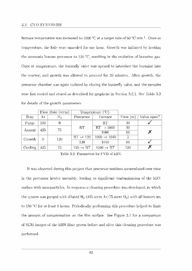
3.2. CVD SYNTHESIS
furnace temperature was increased to 1000 °C at a target rate of 60 °C min-1. Once at
temperature, the foils were annealed for one hour. Growth was initiated by heating
the ammonia borane precursor to 120 °C, resulting in the evolution of borazine gas.
Once at temperature, the butter�y valve was opened to introduce the borazine into
the reactor, and growth was allowed to proceed for 20 minutes. After growth, the
precursor chamber was again isolated by closing the butter�y valve, and the samples
were fast cooled and stored as described for graphene in Section 3.2.1. See Table 3.2
for details of the growth parameters.
Flow Rate (sccm) Temperature (°C)Step Ar H2 Precursor Furnace Time (m) Valve open?
Purge 500 0RT
RT 30 !
Anneal 425 75RT � 1000 30
%1000 60
Growth 0 120RT � 120 1000 � 1040 5
120 1040 60 !
Cooling 425 75 120 � RT 1040 � RT 120 %
Table 3.2: Parameters for CVD of hBN.
It was observed during this project that precursor residues accumulated over time
in the precursor heater assembly, leading to signi�cant contamination of the hBN
surface with nanoparticles. In response a cleaning procedure was developed, in which
the system was purged with diluted H2 (425 sccm Ar/75 sccm H2) with all heaters set
to 150 °C for at least 8 hours. Periodically performing this procedure helped to limit
the amount of contamination on the �lm surface. See Figure 3.1 for a comparison
of SEM images of the hBN �lms grown before and after this cleaning procedure was
performed.
82

3.2. CVD SYNTHESIS
a ba b
Figure 3.1: hBN �lms grown (a) before and (b) after the system had been cleaned ofprecursor residues. Note reduction in the appearance of particles in (b). Scale bar is 2.5 μm.
3.2.3 Tungsten Disulphide
Tungsten disulphide (WS2) domains were grown on the surface of silicon wafers (most
metallic substrates including copper are precluded by the high reactivity of sulphur)
with 300 nm oxide layer (University Wafer), diced into 2 × 2 cm substrates. Sub-
strates were cleaned by ultrasonication in DI water, acetone and IPA for 15 minutes
each. This was followed by cleaning in a 90 W oxygen plasma for 15 minutes. Growth
was performed by two zone vapour transport in a 1� quartz tube in which two dif-
ferent precursors are evaporated in separate furnaces upstream of the substrate. The
�rst (low-temperature; LT) furnace was used to evaporate sulphur powder, while the
second (high-temperature; HT) furnace was used to evaporate WO3 powder and heat
the substrate. 350 mg of sulphur (purum grade, >99.5 %, Sigma-Aldrich) was placed
directly in the furnace tube and centred in the LT furnace. 200 mg of WO3 powder
(puriss. grade, 99.9 %, Sigma-Aldrich) was place in a 1 cm quartz tube that was
placed inside the 1� tube, placed on top of the sulphur powder such that the end was
at the upstream edge of the LT furnace, and the WO3 was centred in the HT furnace.
83
3.2. CVD SYNTHESIS
The clean silicon substrate was placed in the 1� tube, close to the downstream
edge of the HT furnace and supported by an alumina crucible. The system was then
sealed and purged with Ar. The HT furnace was ramped to 470 °C, and once at this
point the LT furnace was ramped to 180 °C, and the HT furnace was increased to
1145 °C, such that the target temperatures were reached simultaneously. The �ow
rate of Ar was reduced once the LT furnace had reached 100 °C. Growth was then
allowed to proceed for around 4 minutes�a shorter time producing smaller isolated
domains, and a longer time leading to larger domains and regions of continuous
�lm. Further extensions to growth time were found to be detrimental to the material
quality, by producing multilayer and non-2D crystals, and so were avoided. After
this time, growth was arrested by reducing the Ar �ow to 10 sccm, and the HT
furnace switched o�. The low temperature furnace was ramped to 400 °C, and once
the HT furnace cooled to 900 °C, the Ar �ow was returned to 500 sccm to purge the
remaining sulphur from the system. The LT furnace was subsequently switched o�,
and the furnaces separated to enable fast cooling of the substrate. See Table 3.3 for
a summary of this procedure. Typical domains grown by this procedure are shown in
Figure 3.2a.
To achieve the continuous �lms used in our production of suspended devices,[1]
we incubated the growth with the HT furnace at 470 °C for ∼5 minutes, while the
LT furnace was increased to 100 °C. Growth was then continued as normal. This
incubation period leads to more nucleation on the surface, without the associated
degradation in quality observed when simply extending the growth time. An example
image of the continuous region is shown in Figure 3.2b. The lines of brighter points
84
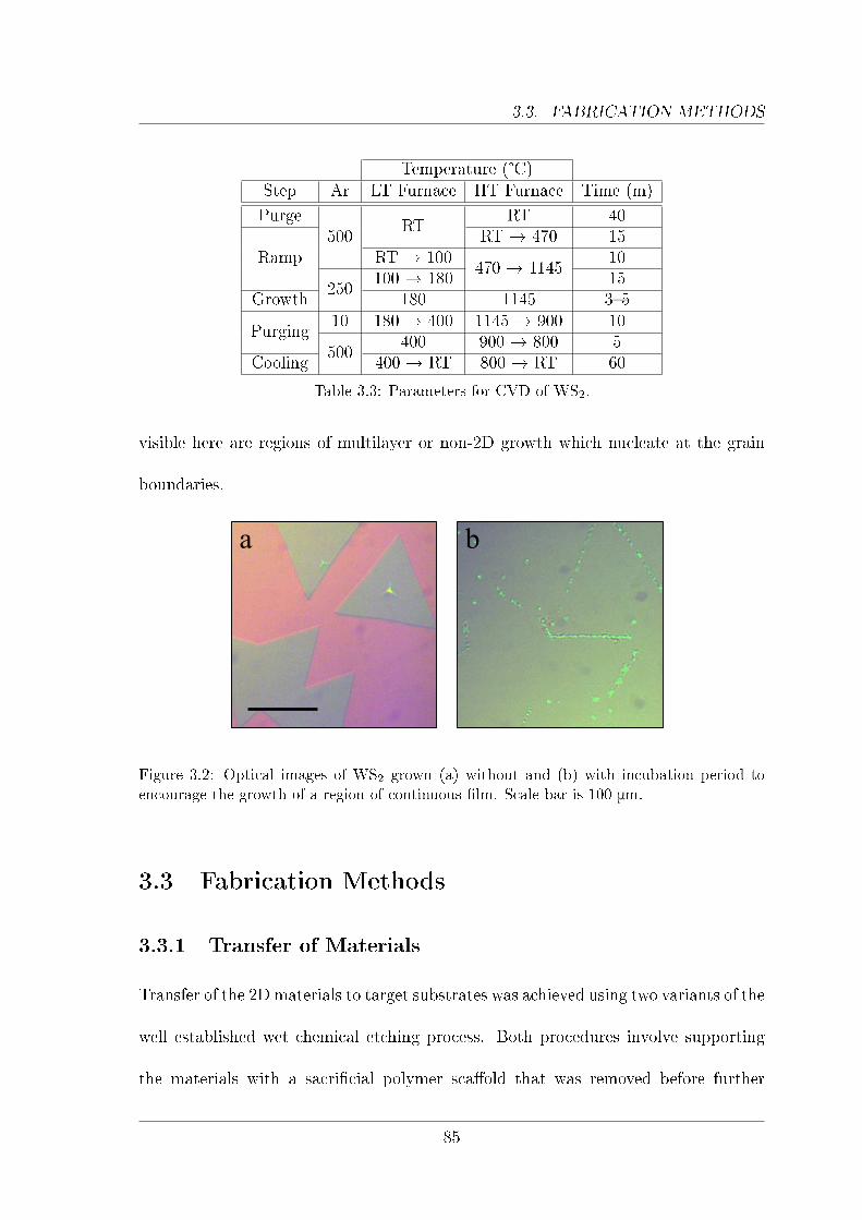
3.3. FABRICATION METHODS
Temperature (°C)Step Ar LT Furnace HT Furnace Time (m)
Purge500
RTRT 40
RampRT � 470 15
RT � 100470 � 1145
10
250100 � 180 15
Growth 180 1145 3�5
Purging10 180 � 400 1145 � 900 10
500400 900 � 800 5
Cooling 400 � RT 800 � RT 60
Table 3.3: Parameters for CVD of WS2.
visible here are regions of multilayer or non-2D growth which nucleate at the grain
boundaries.
a b
Figure 3.2: Optical images of WS2 grown (a) without and (b) with incubation period toencourage the growth of a region of continuous �lm. Scale bar is 100 μm.
3.3 Fabrication Methods
3.3.1 Transfer of Materials
Transfer of the 2D materials to target substrates was achieved using two variants of the
well established wet chemical etching process. Both procedures involve supporting
the materials with a sacri�cial polymer sca�old that was removed before further
85
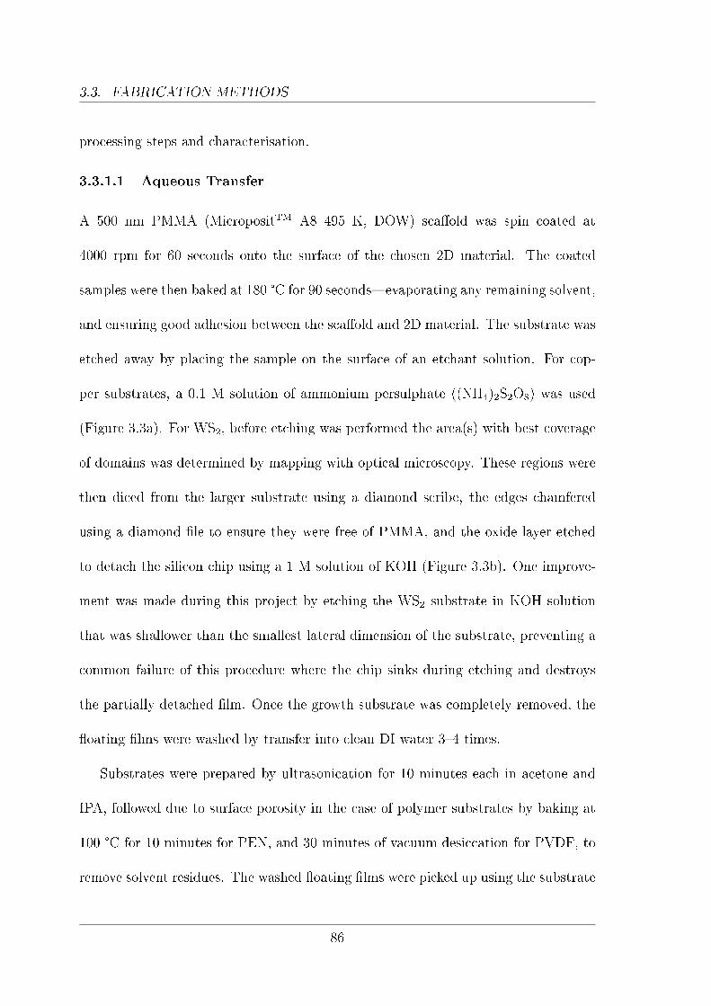
3.3. FABRICATION METHODS
processing steps and characterisation.
3.3.1.1 Aqueous Transfer
A 500 nm PMMA (MicropositTM A8 495 K, DOW) sca�old was spin coated at
4000 rpm for 60 seconds onto the surface of the chosen 2D material. The coated
samples were then baked at 180 °C for 90 seconds�evaporating any remaining solvent,
and ensuring good adhesion between the sca�old and 2D material. The substrate was
etched away by placing the sample on the surface of an etchant solution. For cop-
per substrates, a 0.1 M solution of ammonium persulphate ((NH4)2S2O8) was used
(Figure 3.3a). For WS2, before etching was performed the area(s) with best coverage
of domains was determined by mapping with optical microscopy. These regions were
then diced from the larger substrate using a diamond scribe, the edges chamfered
using a diamond �le to ensure they were free of PMMA, and the oxide layer etched
to detach the silicon chip using a 1 M solution of KOH (Figure 3.3b). One improve-
ment was made during this project by etching the WS2 substrate in KOH solution
that was shallower than the smallest lateral dimension of the substrate, preventing a
common failure of this procedure where the chip sinks during etching and destroys
the partially detached �lm. Once the growth substrate was completely removed, the
�oating �lms were washed by transfer into clean DI water 3�4 times.
Substrates were prepared by ultrasonication for 10 minutes each in acetone and
IPA, followed due to surface porosity in the case of polymer substrates by baking at
100 °C for 10 minutes for PEN, and 30 minutes of vacuum desiccation for PVDF, to
remove solvent residues. The washed �oating �lms were picked up using the substrate
86
3.3. FABRICATION METHODS
and left to dry overnight (Figure 3.3c). To ensure good conformation and adhesion
to the substrate, the samples were baked at 120 °C for 25 minutes, and the PMMA
sca�old was removed by immersing the samples in acetone at 45 °C for at least 3
hours. Subsequent layers were transferred immediately after removal of the PMMA,
minimising the contamination between layers. Due to its low working temperature,
for the transfer of graphene to PVDF conformation was ensured instead by the rede-
position of a layer of diluted PMMA (A1 495 K), and PMMA removal accomplished
in room temperature acetone for 48 hours.
Since acetone was precluded in the transfer onto PMMA used in Chapter 4, a
procedure using a 2 μm �lm of negative photoresist (ma-N 1420, Micro Resist) was
developed instead, due to its solubility in IPA. The transfer was performed as normal,
with a reduced baking temperature of 100 °C (the softbake temperature of ma-N
1420). Removal was performed in IPA at 45 °C for 3 hours.
3.3.1.2 Non-Aqueous Transfer
To reduce contamination with water and facilitate better alignment of the layers, the
non-aqueous technique demonstrated by Sheng et al.[2] was also used. All preparation
was the same up to the point of transfer to the target substrate. At this point, the
�oating �lm was picked up onto a custom piece of apparatus developed for this project
consisting of a small frame holding a hinged piece of glass. This was then placed such
that the free end was on top of one edge of the substrate. IPA was used to carry the
�lm down the ramped cover glass and onto the substrate, which could then be aligned
much more precisely than in the case of aqueous transfer by means of an underlying
87

3.3. FABRICATION METHODS
grid. A schematic of this procedure is shown in Figure 3.3d. Baking and PMMA
removal then followed the same procedure as before.
a
b
c
d
( ) S ONH4 2 2 8
PMMA
IPA
As grownmaterial
Spincoatpolymer scaffold
Etch growthsubstrate
Transfer totarget substrate
Copper Silicon Etchant PEN Cover glass PMMA/2D
Wash freefloating film
Graphene or hBN
WS2
KOH
Figure 3.3: Schematics detailing the di�erent transfer processes. (a) Etching of copper foilfor graphene or hBN transfer. (b) Etching of silicon oxide for WS2 transfer. (c) Aqueoustransfer and (d) non-aqueous transfer.
88

3.3. FABRICATION METHODS
3.3.2 Photolithography
Photolithography, performed using a mask aligner, was used in several di�erent pat-
terning processes. This technique uses UV light to pattern a polymer �lm, and was
favoured over electron-beam lithography for its compatibility with insulating sub-
strates, and its scalability. PEN substrates were �rst cut to size by means of a laser
cutter to ensure proper squareness without damaging the surface �nish. Contamin-
ants and residues from the laser cutting process were then removed by sonication in
acetone and IPA for 10 minutes each before baking at 100 °C for 10 minutes to remove
solvent residues. Once cooled, they were immediately spin coated with appropriate
photoresist and softbaked to remove solvent residues. The majority of devices were
produced using only the positive resist S1813 (MicropositTM S1813 G2, DOW). A
1 μm �lm was produced by spinning at 4500 rpm, followed by a 115 °C softbake for 1
minute. Preparation of silicon substrates followed a similar procedure, without laser
cutting. The substrates were loaded into the mask aligner, aligned to the photomask
(by means of the substrate corners in the case of gold, and deposited gold alignment
marks for subsequent layers), and exposed in hard contact mode.
Once exposed, the photoresist was developed by gentle agitation in the appropriate
developer (MicropositTM 351, DOW, diluted 1:5 in DI water). Increased cleanliness
and removal of resist scum was achieved by dipping the sample in clean developer
following development. Development was completed by rinsing in DI water and drying
by nitrogen gun. Samples were stored under class 1000 cleanroom conditions to avoid
contamination and further UV light exposure. This was especially important when
89

3.3. FABRICATION METHODS
graphene was to be transferred on top of the pattern, since all traditional substrate
cleaning methods were precluded. Exposure and developer times for the various
procedures using S1813 are summarised in Table 3.4 below.
3.3.3 Metallization
3.3.3.1 Thermal Evaporation
Thermal evaporation, a process that uses Joule heating under high vacuum to evap-
orate a layer of the chosen metal onto the target substrate, was used to metallize
contacts de�ned by photolithography. The patterned substrates were attached to the
sample plate by means of Kapton tape and loaded into the evaporator (Edwards 360).
Evaporation was typically performed once the chamber was pumped down to 2 Ö 10-6
mbar. Electrodes were deposited in gold to a typical thickness of 100 nm, with the
deposition kept at a low rate of 0.1�0.2 nm s�1 to reduce the �ux of heat into the
substrate, thereby minimising thermal damage.
Chromium is commonly used as an adhesion layer for gold �lms but was not used
for the �exible devices fabricated here as it has been shown to cause embrittlement
of deposited metal �lms.[3] Without chromium it was found that the adhesion of gold
to PEN was very poor, resulting in destruction of the deposited contacts when lift-
o� was attempted. As a result, another means of improving adhesion was required.
A post lithography treatment in 90 W oxygen plasma for 2 minutes was used to
functionalise the PEN surface and increase the roughness in the exposed parts, with
the remaining substrate area protected from damage by the photoresist. Once metal
deposition was complete, the samples were heated on a hotplate at 120 °C (Tg of
90

3.3. FABRICATION METHODS
PEN) to increase the conformation between the gold and PEN. Further details are
available in Chapter 5.
3.3.3.2 Lift-o�
Lift-o� of the gold electrodes was performed by immersing the samples in acetone
at 45 °C for at least 3 hours, and the majority of the loosened gold removed by
agitation using a pipette. Any remaining gold was removed using ultrasonication for
approximately 1 minute, performed in 15 second intervals until lift-o� was complete.
3.3.4 Graphene Patterning
3.3.4.1 Oxygen Plasma Etching
Conventionally, graphene is patterned using oxygen plasma. This is performed by �rst
transferring a layer of graphene onto the desired substrate, and photolithographically
producing a positive image of the desired structures on its surface. The exposed
graphene is subsequently etched away using oxygen plasma, with typical parameters
being 60 W for 2 minutes. This process is very e�ective for hard substrates like
silicon and quartz, but is inappropriate for soft matter such as the polymers used
throughout this work, as detailed in Chapter 5. For this reason, the majority of
devices were instead patterned using the method described below.
3.3.4.2 Lift-o�
Based on the work of Trung et al.,[4] a modi�ed lift-o� procedure was developed to pat-
tern the graphene without etching. The desired structures were photolithographically
de�ned in negative using a positive photoresist (S1813) on a clean substrate surface.
91
3.4. IMAGING TECHNIQUES
An increased development time compared to that used for metal patterning was used,
producing more rounded edges to enable better conformation of the graphene �lm. A
graphene �lm with a PMMA sca�old of signi�cantly reduced thickness (100 nm, to
further facilitate conformation to the pattern; cf. the 500 nm �lms used convention-
ally) was transferred on top of this pattern, dried, and baked for 6 hours at 80 °C to
ensure conformation between the graphene and substrate surface. This lower baking
temperature enabled the �lm to relax slowly and avoided outgassing from the S1813.
To produce the thinner sca�old, the spin coating procedure described in Section 3.3.1
was repeated twice using A1 495 K PMMA (A8 495 K diluted 1:7 in anisole).
The excess graphene was then removed by dissolving the resist and sca�old in
acetone at 45 °C for 3 hours, followed by 30 seconds of ultrasonic treatment to scission
the free �oating �lm. The patterned structure was then washed of any remaining
residues using IPA, and dried by nitrogen gun. The development of this procedure is
described in greater detail in Chapter 5.
Process Dose (mJ cm-2) Development (s)
Metal electrode deposition 45 50
Graphene patterningPlasma 45 60Lift-o� 25 70
Table 3.4: Exposure and development times for S1813 based photolithographic processes.
3.4 Imaging Techniques
3.4.1 Optical Microscopy
Optical microscopy was used to examine and characterise many of the samples�
predominantly the as grown WS2 and fabricated heterostructures and devices. Cus-
92

3.4. IMAGING TECHNIQUES
tom built microscopes with objective lenses ranging from 4�50× magni�cation were
used for preliminary characterisation, with higher resolution images taken using a
system with 100× magni�cation. The main purpose of this was to assess the qual-
ity of the samples, as well as to map the WS2 prior to dicing and transfer, before
proceeding with subsequent fabrication and characterisation steps. Due to the poor
contrast of graphene on PEN high resolution imaging was important during the char-
acterisation of patterned graphene in Chapter 5, where the small scale features and
defects required high quality images and signi�cant enhancement to be resolved. Im-
age enhancement and analysis was performed using the ImageJ software package.
3.4.2 Scanning Electron Microscopy
Scanning electron microscopy (SEM) was used extensively to study each of the 2D
materials before and after transfer, as well as after microfabrication techniques and
after optoelectronic measurements had been performed. A Hitachi S-4300 SEM was
used, with a typical accelerating voltage of 3 kV and a beam current of 11 μA .
This low accelerating voltage enables good contrast of the 2D materials, without
signi�cant over-penetration of the electrons into the underlying substrate, which can
hamper image quality. Conductive substrates were grounded by using carbon tape to
a�x the substrate to the SEM stub, and insulating substrates were only imaged where
graphene was present to prevent substrate charging, with the graphene connected to
the specimen stub by �rst depositing a gold or silver paint (RS Components) electrode,
and grounding this with carbon tape. Cross-sectional SEM was performed by �rst
cleaving the substrate using a diamond scribe, and �xing the sample perpendicular
93

3.4. IMAGING TECHNIQUES
to the stage by means of a cross-section stub. Image enhancement and analysis was
performed using the ImageJ software package. For measuring the average spacing of
two lines (e.g. the measurement of �lm thickness in Chapter 4 and electrode spacing
in Chapter 5), the Distance Between Lines plug-in for ImageJ was used.
3.4.3 Atomic Force Microscopy
Atomic force microscopy (AFM) was used to provide topographic information inac-
cessible by other methods. Two systems were used in tapping mode under ambient
conditions: an Asylum Research MFP-3D with silicon AC160TS cantilever tips, and
an Agilent 5400 with Mikromasch NSC35/ALBS tips. Scan rates of 0.5 lines per
second were used to produce maps of the surface. These were analysed to produce
line pro�les and surface roughness measurements using the Gwyddion software pack-
age.
3.4.4 Magnetic Resonance Imaging
Magnetic resonance imaging (MRI) was performed using a 7 T, 210 VNMRS ho-
rizontal bore preclinical imaging system with 120 mm bore gradient insert (Varian
Inc.). A 25 mm ID quadrature birdcage coil with 35 mm RF window length (Rapid
Biomedical GmbH) was used for transmission and reception of RF signals. A con-
stant TR, steady-stage respiration gated gradient echo imaging procedure was used
for in vivo imaging. Typical parameters were TR = 16.8 ms, TE = 12 ms, FA = 10°,
THK = 2 mm, in plane resolution = 250 μm and image matrix = 128 × 128. Adapted
from Gilchrist et al.[5]
94
3.5. OPTICAL SPECTROSCOPY
3.4.5 Computed Tomography Imaging
For computed tomography (CT) imaging, the following settings were used: X-ray
tube operated at 50 kV and 500 μA, a 300 ms exposure time per projection, 540
projections, and 360° continuous rotation, a binning factor of 4 and a matrix size of
3072 × 2048. Images were reconstructed using the Feldkamp algorithm. Adapted
from Kersemans et al.[6]
3.5 Optical Spectroscopy
3.5.1 Raman Spectroscopy
Raman spectroscopy was performed using an imaging confocal Raman spectrometer
(JY Horiba Labram Aramis) coupled to a 532 nm frequency doubled Nd:YAG laser.
Rapid pro�ling was performed using a 600 slits mm-1 grating, and when �ne resolution
was required a 1800 slits mm-1 grating was used. Owing to their di�ering Raman shifts
and signal intensities, di�erent parameters were required for each material. Typical
values are summarised in Table 3.5. In some cases, individual points were examined
at pertinent locations on the sample, while at others the mapping function of the
spectrometer was used to gain insight into the distribution over an area.
Material Laser Power (μW) Acq. Time (s) Accumulations Range (cm-1)
Graphene 587 5 5 1200�3000hBN 587 10 30 1300�1500WS2 1600 5 3 200�550
Table 3.5: Summary of typical Raman parameters.
95

3.5. OPTICAL SPECTROSCOPY
3.5.2 Photoluminescence Spectroscopy
Photoluminescence (PL) spectroscopy was performed using a custom built spectro-
meter, equipped with a diode-pumped solid-state 532 nm laser (Thorlabs DJ532-40),
and coupled to a charge-coupled device (CCD) spectrometer (Princeton Instruments
Acton SP-2300 spectrometer with Princeton Instruments PIXIS 100 CCD). The typ-
ical acquisition parameters were 1.1 mW or ∼4 kW cm-2 laser power, and 1 second
acquisition time. The measured spectra were corrected for the PEN background
prior to analysis using Matlab, and the peak properties determined by Lorentzian or
Gaussian �tting.
PL spectra are generally captured in units of wavelength, but (due to non-linearity
and resultant distortion of �tted peak shapes) must be converted into units of en-
ergy before analysis. This is performed using the Planck�Einstein relation (Equa-
tion 3.1):[7]
E = hν =hc
λ(3.1)
Where E is energy, h is the Planck constant, c is the speed of light, ν is frequency,
and λ is wavelength. In addition, the intensity (I ) must be rescaled by the Jacobian
transformation (Equation 3.2):[7]
IE =Iλhc
E2(3.2)
Once this has been performed, the spectra can in principle be decomposed into
96
3.6. STRAINED MEASUREMENTS
their various contributions.
3.6 Strained Measurements
In many of the spectroscopic and optoelectronic measurements in Chapters 4 & 5,
a method to apply strain in situ was required. This was achieved using a custom
built holder, by collapsing radius test�where the substrate is controllably bent, and
the strain in the surface calculated from elasticity theory. The holder was mounted
directly to the sample stage and could be moved in half-mm increments, enabling a
maximum strain >2.5 % to be applied in the case of the 250 μm substrates used here.
The strain in the substrate surface was calculated as outlined by McCreary et al.[8]
and others,[9�12] using Equation 3.3:
ε =tsinθ
d(3.3)
Here, ε is the strain in the substrate surface, θ is the angle of the tangent of the
substrate at the point of contact, d is the grip separation of the holder as measured
by the scale, and t is the substrate thickness. See Figure 3.4 for more details.
97

3.6. STRAINED MEASUREMENTS
a
Grips
ScaleSubstrate
Laser
θ
Stagemount
Film
b
Figure 3.4: Details of the holder used to apply strain in situ. (a) Schematic of the strainholder detailing key components. (b) Image of the strain holder with blank substrate inplace.
In this measurement geometry, when force is applied to the substrate the stress
at the �lm edge will be lower than at its centre, with load transferred through shear
forces. This leads to a distribution of strain across a stress transfer length Lt (i.e.
when x < Lt , with x = 0 at the �lm edge), beyond which the stress may simply be
calculated from the Young's modulus by:
σf = εEf (3.4)
Where σvf is the stress in the �lm and E f is its Young's modulus. Prior to yield
of the interface the magnitude of stress transferred from the substrate to the �lm
depends on the di�ering dimensions and sti�ness values of the two materials�the
sti�er �lm experiencing a smaller stress and strain than the more compliant substrate.
This situation is shown schematically in a cross section of the �lm and substrate in
Figure 3.5a.
When the interface begins to yield, the depiction in Figure 3.5a is no longer valid.
98

3.6. STRAINED MEASUREMENTS
Instead, the magnitude of interfacial shear τf is assumed to be constant within the
stress transfer length (i.e. when x < Lt) and can be calculated by considering a thin
segment perpendicular to the load axis of length δx and at a distance x from the �lm
edge (of width w and thickness t), as shown in Figure 3.5b.
σ + δσf f
τf
σf
x
δx
t
w
Film
Substrate
σσ
StrainedUnstrained
σσ
a
b
Figure 3.5: Stresses acting on a thin �lm where (a) the interface does not yield and (b)where it does. The vertical lines in (a) are plotted to display the displacements when the�lm is stressed.
The total force on the element shown in Figure 3.5b must be zero to maintain equi-
librium, therefore:
(σf + δσf )wt− σfwt− τfwδx = 0 (3.5)
Collecting terms and simplifying leads to:
δσfδx
=τft
(3.6)
Integrating under the assumption that σvf = 0 when x = 0 gives the equation:
99
3.7. ELECTRICAL MEASUREMENTS
σf =τfx
t(3.7)
Inserting Equation 3.4 with a measured value for the strain in the �lm (εf ) enables
estimation of the interfacial shear stress:
τf =εfEf t
x(3.8)
This description is based on the work of Hull & Clyne.[13]
3.7 Electrical Measurements
Electrical measurements were performed using two separate pieces of equipment:
a Keithley 2400 SourceMeter® for I-V and sheet resistance measurements; and a
Biopac® MP150 with attached DA100C ampli�er, modi�ed to further increase amp-
li�cation by a factor of 10, for high speed potential measurements.
3.7.1 Keithley 2400 SourceMeter
3.7.1.1 I-V
I-V measurements were used to characterise the all-2D photodetector devices de-
scribed in Chapter 5. The devices were mounted to a microscope stage, using the
strain holder described in Section 3.6 in the case of �exible devices, and contacted
by two tungsten probes (Sel-Tek Signatone® SE-T). The probes were connected to
the unit by shielded BNC cables to mitigate electrical noise. A bias was applied in
both directions, and the current measured at incremental points. The measurements
were automated using Python with the PyMeasure package. Laser irradiation was
provided by means of a diode-pumped solid-state 532 nm Thorlabs DJ532-40 laser.
100
3.7. ELECTRICAL MEASUREMENTS
3.7.1.2 Sheet resistance
Sheet resistance (Rs�measured in Ohms, but denoted as Ω/0 to avoid confusion
with the bulk resistance R, also in Ohms) is a measurement used to characterise thin
�lms of uniform thickness that is useful because it removes the in�uence of geometric
factors and contact resistance from the measurement. This measurement can be
made using a number of di�erent techniques. Here the van der Pauw method was
used, where ideally point but in practice small, Ohmic contacts are made to the four
corners of a square specimen, and numbered 1�4 . A current is then applied between
two contacts on the same edge (e.g. 1 & 2), and the resulting potential measured
across the other two corners (3 & 4). The resistance (here R1 2, 3 4) is then calculated
using Ohm's Law. This measurement is repeated at 90° to produce R2 3, 4 1. Rs can
then be calculated iteratively using Equation 3.9:[14]
e−πR12,34
Rs + e−πR23,41
Rs = 1 (3.9)
To improve the precision of the measurement it was repeated in all possible per-
mutations, viz.: reversed along each side (R1 2, 3 4 & R2 1, 4 3), �ipped across the
centre (R3 4, 1 2 & R4 3, 2 1), and similar for R2 3, 4 1. The sheet resistance equation
then becomes Equation 3.10:[14]
e−πRH
RS + e−πRVRs = 1 (3.10)
In which:
RH =R12,34 +R34,12 +R21,43 +R43,21
4
101

3.8. ANIMAL HANDLING
And similar for RV.
The measurements and calculation of Rs were automated using a Python script
written by Dr. Zhengyu He (modi�ed from original by Dr Chris Allen).
3.7.2 Biopac MP150 & DA100C
The respiratory monitors described in Chapter 6 produce short, transient signals that
require measurement rates exceeding the capabilities of the Keithley 2400 SourceMeter®.
The MP150 provides high measurement rates and signal to noise ratio, with adjustable
signal ampli�cation provided by the DA100C unit, enabling accurate measurement of
the generated potential. The devices were connected to a shielded potential divider
to reduce electrical noise and enable adjustable control of the input signal intensity,
and the potential between the two sides as a result of small mechanical deformations
measured at a rate of 1 kHz. The reduction of electrical noise was critical here due to
the high ampli�cation used. By enclosing all components up to the sensor in a shield,
and using twisted pair leads, the noise was reduced by several orders of magnitude.
Measurements were recorded using the AcqKnowledge® software package.
3.8 Animal Handling
Animals were handled in accordance with the UK Animals Scienti�c Procedure Act
of 1986, under licences approved by the UK Home O�ce, and with the approval of
the University of Oxford ethical review committee, under PPL 30/3266. All in vivo
work (animal handling, and MRI and CT imaging) was carried out by Dr Veerle
Kersemans, under PIL IC45C45D9. Details of animal preparation and handling are
102

3.8. ANIMAL HANDLING
adapted from Gilchrist et al.[5]
3.8.1 Animal Preparation
CBA mice (Charles River) were housed in individual ventilated cages, maintained at
22 °C and 50 % humidity, with a 12 hour dark/light cycle. Animals were provided
with autoclaved bedding material, cage enrichment, �ltered water ad libitum, and
a certi�ed rodent diet. Every practical e�ort was made to minimise su�ering, in
accordance with the 3Rs of animal handling, though one animal had to be euthanised
on welfare grounds. 1�4 % iso�urane in air was used to induce anaesthesia, the
condition of which was typically monitored using our piezoelectric sensor as described
in Chapter 6, and maintained at 40�80 breaths per minute.
3.8.2 Homeothermic Maintenance
Rectal temperature was measured using a �bre-optic thermometer. This temperature
was continuously monitored and body temperature maintained at ∼35 °C by means
of the carbon-�bre heating system demonstrated previously by Gilchrist et al.[5]
103

Bibliography
[1] Y. Fan, A. W. Robertson, X. Zhang, M. Tweedie, Y. Zhou, M. H. Rummeli,H. Zheng, J. H. Warner, �Negative Electro-conductance in Suspended 2D WS2Nanoscale Devices�, ACS Applied Materials and Interfaces 2016, 32963�32970.
[2] Y. Sheng, W. Xu, X. Wang, Z. He, Y. Rong, J. H. Warner, �Mixed MultilayeredVertical Heterostructures Utilizing Strained Monolayer WS2�, Nanoscale 2016,8, 2639�2647.
[3] M. J. Cordill, A. Taylor, J. Schalko, G. Dehm, �Fracture and Delamination ofChromium Thin Films on Polymer Substrates�,Metall. Mater. Trans. A 2010,41, 870�875.
[4] T. N. Trung, D.-O. Kim, J.-H. Lee, V.-D. Dao, H.-S. Choi, E.-T. Kim, �Simpleand Reliable Lift-O� Patterning Approach for Graphene and Graphene-AgNanowire Hybrid Films�, ACS Applied Materials & Interfaces 2017, 9, 21406�21412.
[5] S. Gilchrist, A. L. Gomes, P. Kinchesh, V. Kersemans, P. D. Allen, S. C.Smart, �An MRI-Compatible High Frequency AC Resistive Heating System forHomeothermic Maintenance in Small Animals�, PLoS ONE 2016, 11, 0164920.
[6] V. Kersemans, P. Kannan, J. S. Beech, R. Bates, B. Irving, S. Gilchrist, P. D.Allen, J. Thompson, P. Kinchesh, C. Casteleyn, J. Schnabel, M. Partridge,R. J. Muschel, S. C. Smart, �Improving in Vivo High-Resolution CT Imagingof the Tumour Vasculature in Xenograft Mouse Models Through Reduction ofMotion and Bone-Streak Artefacts�, PLoS ONE 2015, 10, 0128537.
[7] P. Kambhamptai, �Get the Basics Right: Jacobian Conversion of Wavelengthand Energy Scales for Quantitative Analysis of Emission Spectra�, Journal ofPhysical Chemistry Letters 2013, 4, 3316�3318.
[8] A. McCreary, R. Ghosh, M. Amani, J. Wang, K. A. N. Duerloo, A. Sharma,K. Jarvis, E. J. Reed, A. M. Dongare, S. K. Banerjee, M. Terrones, R. R.Namburu, M. Dubey, �E�ects of Uniaxial and Biaxial Strain on Few-LayeredTerrace Structures of MoS2 Grown by Vapor Transport�, ACS Nano 2016, 10,3186�3197.
[9] H. J. Conley, B. Wang, J. I. Ziegler, R. F. Haglund, S. T. Pantelides, K. I. Bo-lotin, �Bandgap Engineering of Strained Monolayer and Bilayer MoS2�, NanoLetters 2013, 13, 3626�3630.
104

[10] X. Wang, A. M. Jones, K. L. Seyler, V. Tran, Y. Jia, H. Zhao, H. Wang, L.Yang, X. Xu, F. Xia, �Highly Anisotropic and Robust Excitons in MonolayerBlack Phosphorus�, Nat. Nanotechnol. 2015, 10, 517�521.
[11] T. M. G. Mohiuddin, A. Lombardo, R. R. Nair, A. Bonetti, G. Savini, R. Jalil,N. Bonini, D. M. Basko, C. Galiotis, N. Marzari, K. S. Novoselov, A. K. Geim,A. C. Ferrari, �Uniaxial Strain in Graphene by Raman Spectroscopy: G PeakSplitting, Grüneisen Parameters, and Sample Orientation�, Physical Review B- Condensed Matter and Materials Physics 2009, 79, 205433.
[12] M. Matthewson, C. R. Kurkjian, S. T. Gulati, �Strength Measurement of Op-tical Fibers by Bending�, Journal of the American Ceramic Society 1986, 69,815�21.
[13] D. Hull, T. W. Clyne in An Introduction to Composite Materials, 1996.
[14] L. J. van der Pauw, �A Method of Measuring the Resistivity and Hall Coef-�cient on Lamellae of Arbitrary Shape�, Philips Technical Review 1958, 20,220�224.
105


Chapter 4
Heterolayer-Independent
Inhomogeneous Strain Release in
Strained WS2-Containing
Heterostructures
4.1 Introduction
Before the full potential of 2D materials can be achieved in �exible electronics, a
more comprehensive understanding is needed of the in�uence of strain on the various
heterostructures likely to be found in these devices. As discussed in Chapter 2,
there are numerous ways in which the local environment can modify the properties
of 2D materials.[1,2] Like other materials, strain can also in�uence their properties
signi�cantly.[3�5]
107

4.1. INTRODUCTION
As described in Section 2.2.4, friction in 2D materials is complex. The van der
Waals forces that hold the layers together are comparatively weak, and so incomplete
strain transfer and sliding are likely to be a factor in their response to strain.[6,7]
Furthermore, the unique ease of out-of-plane deformation can lead to distortion and
folding of the �lm at the nanoscale in response to mechanical stimuli.[8]
In an e�ort to understand the in�uence these e�ects may have in vertically stacked
2D layered systems of di�erent materials, herein we examine the changes in the photo-
luminescence (PL) spectra of the direct bandgap TMD tungsten disulphide (WS2) in
several di�erent heterostructure con�gurations involving graphene and boron nitride
(hBN), in response to strain. Poly(ethylene naphthalate) (PEN), a material com-
monly employed in �exible electronics, was used as the substrate due to its high chem-
ical, thermal and hydrolytic resistance.[9] The chosen heterostructures were (stacked
vertically from top to bottom): WS2/PEN, WS2/hBN/PEN, WS2/graphene/PEN,
and WS2/hBN/graphene/PEN, representing two possible device channels, contacts
and gated channels respectively. Chemical vapour deposition (CVD) was used to
grow the 2D materials, to demonstrate the reproducibility of these �ndings and their
applicability to materials suitable for large scale manufacture.
108
4.2. RESULTS AND DISCUSSION
4.2 Results and Discussion
All materials were grown via CVD, as described in Section 3.2, producing large do-
mains of WS2 (Figure 4.1a), and continuous �lms of typically bilayer graphene and
hBN (Figure 4.1b & 4.1c). Quality and coverage were determined by optical micro-
scopy and scanning electron microscopy (SEM). Raman spectroscopy was performed
to characterise the �lms and determine the layer number (Figure 4.1d�4.1f). These
represent typical spectra taken from each material, though the position of the Raman
peaks can deviate due to doping and strain. The ripples visible in Figure 4.1b & 4.1c
will lead to local variations of strain, though as we similarly observe later in the PL
measurements the size of the laser spot exceeds the size of these ripples and so the
Raman signal represents an average across the resulting strain distribution. Despite
its sensitivity to strain, Raman was not used for measurements of the heterostruc-
tures on PEN as the large background signals produced by this polymer were found
to obscure the signals from the 2D materials.[10]
We used the well-established wet chemical etching technique to remove the growth
substrate, with transfer predominantly achieved using wet/aqueous transfer (aq.).
This was compared with our previously reported non-aqueous transfer technique
(non-aq.), in which isopropyl alcohol is used to displace water, as this can modu-
late interlayer interactions by reducing trapped interfacial contamination.[11] Further
information and schematics of the two processes are provided in Section 3.3.1. The
heterostructures were stacked layer-by-layer from 1 × 1 cm �lms of graphene and
hBN, and domains of WS2 typically 100�200 µm in size.
109

4.2. RESULTS AND DISCUSSION
PL measurements were performed on the di�erent heterostructures (shown schem-
atically in Figure 4.1g) before, during and after the application and relaxation of
strain by bending. The maximum strain was 2.5 %, which was deemed to easily
accommodate the maximum strain that real devices will experience.[12] Application
and relaxation of strain was repeated for a further 2�3 cycles, after which point the
PL changes were observed to stabilise.
2LA(M)E
1
2G
c
5 µm
A1G G 2D
d e fBilayerMultilayer
Inte
nsi
ty (
a.u.)
Raman Shift (cm )-1
Inte
nsi
ty (
a.u.)
Raman Shift (cm )-1
Inte
nsi
ty (
a.u.)
Raman Shift (cm )-1
300 350 400 450 1500 2000 2500 1300 1350 1400
Graphene
a
200 µm
E2G
b
5 µm
WS2 hBN
WS2
PEN
WS2
GrPEN
WS2
hBNPEN
WS2
hBN
PENGr
g
Figure 4.1: Characterisation of the studied 2D materials and schematics of their con�gur-ations in heterostructures. (a) Optical (200 µm scale bar) and (b,c) SEM (5 µm scale bar)images of the as grown WS2, graphene and boron nitride, respectively. (d�f) Raman spec-tra from the same, showing: (d) the combined 2LA(M)/E1
2G (second order LA/in-plane,individual contributions revealed by Lorentzian �tting, other peaks omitted) and A1G (out-of-plane);[13] (e) the G (sp2 speci�c) and 2D (second order, speci�c to graphitic materials);[14]
and (f) the E2G (sp2 speci�c, analogous to the G peak in graphene)[15] characteristic Ra-man modes, respectively. The ratio of the peak intensities indicates that WS2 is monolayer(d) and that graphene is bilayer with small multilayer islands (e), and the position of thepeak indicates that the hBN in (f) is bilayer. (g) Schematic illustrations showing the layerordering of the four heterostructures.
All measurements were carried out using a spectrometer and 532 nm laser, with
strain applied in situ by collapsing radius test using a custom built holder mounted to
110
4.2. RESULTS AND DISCUSSION
the sample stage. See Sections 3.5.2 & 3.6 for more details. The thickness of the 2D
materials can be neglected from the calculation of strain since it is at least 5 orders
of magnitude less than the substrate (∼0.8 nm for bilayer graphene[16] and hBN[15]
and 0.6 nm for WS2[17]).
Due to the convex shape of the substrate as strain is applied, it was only possible to
measure the central region of the specimen under tension. The number of measurable
WS2 domains was optimised by mapping their positions on the growth substrate to
determine the area with the best coverage of high quality domains, and aligning this
to the centre of the PEN substrate (see Figure 3.3 in Section 3.3.1 for more details).
This had the advantage of con�ning our measurements to a region of approximately
uniform strain.
The position and intensity of the PL peak is strongly dependent on the laser power
density. Renormalisation leads to a redshift of the peak with increasing incident power
(Figure 4.2a),[18,19] and intensity increases with laser power due to an increased gener-
ation of excitons, though this begins to saturate at higher laser powers (Figure 4.2b).
For this reason we ensured a constant laser power of 1.1 mW or ∼4 kW/cm-2 by
controlling the temperature and current supplied to the laser diode, and ensuring
consistent focus of the microscope. This was su�cient to provide an adequate signal-
to-noise ratio, without inducing signi�cant thermal e�ects.[20,21]
The PL spectrum of WS2 comprises two component emissions arising from the re-
combination of excitons (A) and trions (A-), the latter being quasiparticles composed
of an exciton bound to either a hole or, in this case, an electron due to the intrinsic
n-type doping of CVD-grown WS2.[17,22,23] Trion emission leads to broadening of the
111
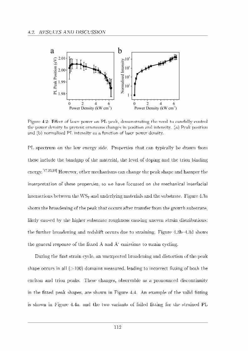
4.2. RESULTS AND DISCUSSION
0 2 4 6Power (kW cm )Density
-2
1.98
1.99
2.00
2.01P
LP
eak P
osi
tion (
eV)
0 2 4 6Power (kW cm )Density
-2
1
102
104
106
108
Norm
alis
ed I
nte
nsi
ty
a b
Figure 4.2: E�ect of laser power on PL peak, demonstrating the need to carefully controlthe power density to prevent erroneous changes in position and intensity. (a) Peak positionand (b) normalised PL intensity as a function of laser power density.
PL spectrum on the low energy side. Properties that can typically be drawn from
these include the bandgap of the material, the level of doping and the trion binding
energy.[17,22,23] However, other mechanisms can change the peak shape and hamper the
interpretation of these properties, so we have focussed on the mechanical interfacial
interactions between the WS2 and underlying materials and the substrate. Figure 4.3a
shows the broadening of the peak that occurs after transfer from the growth substrate,
likely caused by the higher substrate roughness causing uneven strain distributions;
the further broadening and redshift occurs due to straining. Figure 4.3b�4.3d shows
the general response of the �tted A and A- emissions to strain cycling.
During the �rst strain cycle, an unexpected broadening and distortion of the peak
shape occurs in all (>100) domains measured, leading to incorrect �tting of both the
exciton and trion peaks. These changes, observable as a pronounced discontinuity
in the �tted peak shapes, are shown in Figure 4.4. An example of the valid �tting
is shown in Figure 4.4a, and the two variants of failed �tting for the strained PL
112

4.2. RESULTS AND DISCUSSION
1st
2nd
3rd
4th
RelaxApply
0.0 0.5 1.0 1.5 2.0 2.50.4
0.6
0.8
1.0
1.2
1.4
1.6
Norm
alis
ed I
nte
nsi
ty
Strain (%)
b
Fit Component:
ExcitonTrion
Total
Peak Position (eV)
PL
Inte
nsi
ty (
a.u
.)
1.80 1.90 2.00 2.10
After trans.Max. Strain
Relaxed
Pre-transfer
a
1st
2nd
3rd
4th
RelaxApply
Pre transfer0.0 0.5 1.0 1.5 2.0 2.5
1.86
1.88
1.90
1.92
1.94
1.96
Tri
on P
osi
tio
n(e
V)
Strain (%)
Relax
Apply
1st
2nd
3rd
4th
RelaxApply
Pre transfer0.0 0.5 1.0 1.5 2.0 2.5
1.92
1.94
1.96
1.98
2.00
Exci
ton
Posi
tion
(eV
)
Strain (%)
Relax
Apply
dc
Figure 4.3: Example spectra and analysis of one of the studied heterostructures. (a) PLspectra of WS2 taken before and after transfer, at maximum strain, and after strain wasrelaxed for the WS2/graphene/PEN aq. heterostructure. Note that Lorentzian �ts wereused to extract information about the exciton and trion peaks on the pre-transfer spectrum,while due to broadening Gaussian �ts were used post-transfer. (b) Changes in total emissionintensity across three strain cycles in the WS2/graphene/PEN non-aq. heterostructure asstrain is applied and relaxed, and a fourth measurement at 0 % strain. Changes in (c)exciton (A) and (d) trion (A-) positions for same. Pre-transfer values and standard errorsare also indicated. Note stabilisation to a hysteresis loop after the �rst application of strainfor both A and A- peaks.
spectrum are shown in Figure 4.4b & 4.4c. This accounts for the increase in the
standard error of the peak intensity and trion position shown in Figure 4.3b�4.3d.
Our reasoning for the evolution of the peak shape is as follows. After transfer
the peak is redshifted by two factors. First, a tensile strain is induced in the layers,
arising from thermal mismatch and conformation of the sheet to the rough PEN
surface. Second, the lower relative permittivity of the PEN substrate, compared to
113

4.2. RESULTS AND DISCUSSION
1.80 1.90 2.00 2.10
PL
Inte
nsi
ty(a
.u.)
Energy (eV)
Spectrum
Exciton
Trion
Total
1.80 1.90 2.00 2.10
PL
Inte
nsi
ty(a
.u.)
Energy (eV)1.80 1.90 2.00 2.10
PL
Inte
nsi
ty(a
.u.)
Energy (eV)
1.80 1.90 2.00 2.10
PL
Inte
nsi
ty(a
.u.)
Energy (eV)
Bonded
Debonding
Debonded
dc
a b
Figure 4.4: Fitting of exciton and trion peaks to the PL spectra. (a) Valid �tting of theunstrained PL signal. (b,c) Two variants of failed �tting of the strained spectrum, withdiscontinuities in peak position and intensity. (d) An approximation of the peak shapeproduced by summing multiple spectra over a distribution of energies.
the SiO2 that the WS2 was grown on, increases the binding energy of the excitons,
thus lowering the energy released during recombination.[9,24] When strain is applied,
there is initially complete uptake of the applied strain by the WS2. Once a threshold
of ∼0.7 % strain is passed, there is partial debonding and loss of coherency between
the 2D materials and underlying substrate that leads to broadening of the PL peak.
Once the strain is relaxed, as shown in Figure 4.3a there is a lingering blueshift relative
to the initial position that is only partially recovered, caused by the debonding of the
layers releasing the built in tensile strain described above. With this strain released,
114
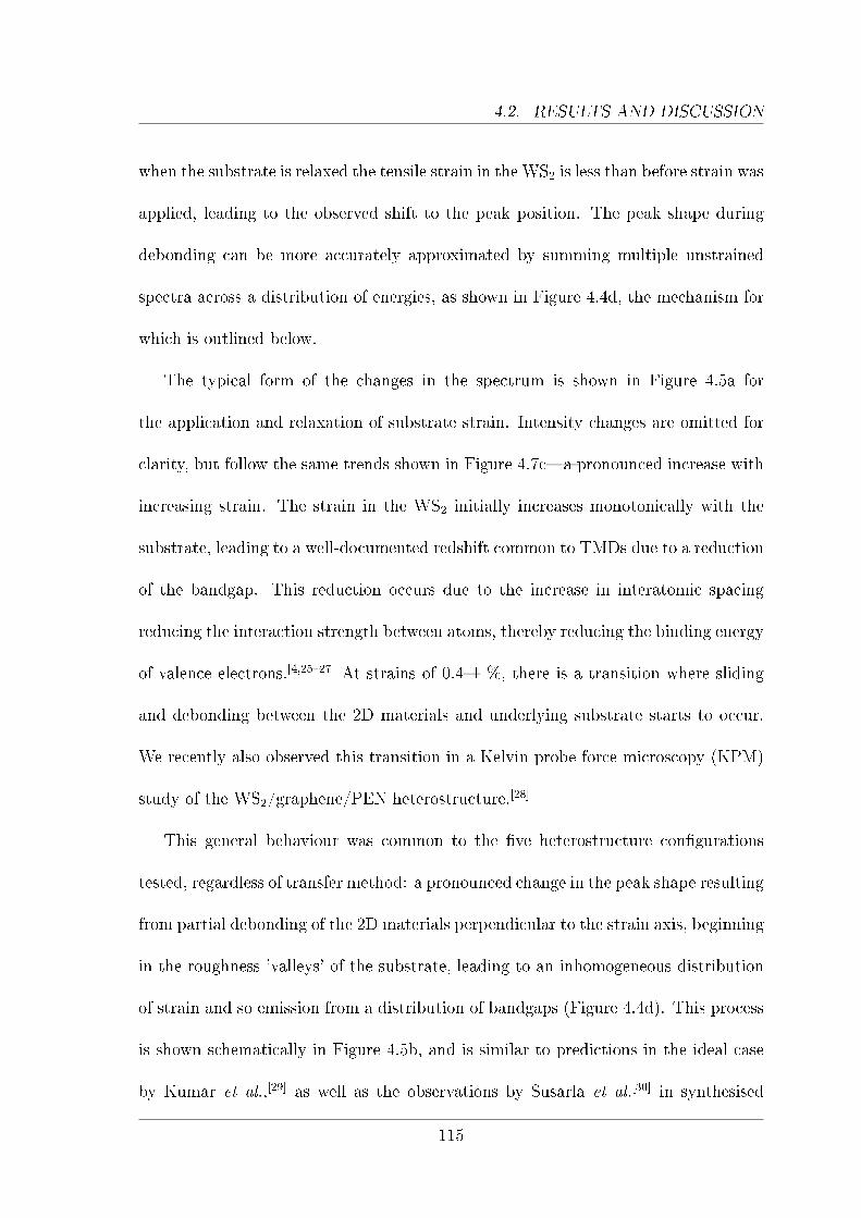
4.2. RESULTS AND DISCUSSION
when the substrate is relaxed the tensile strain in the WS2 is less than before strain was
applied, leading to the observed shift to the peak position. The peak shape during
debonding can be more accurately approximated by summing multiple unstrained
spectra across a distribution of energies, as shown in Figure 4.4d, the mechanism for
which is outlined below.
The typical form of the changes in the spectrum is shown in Figure 4.5a for
the application and relaxation of substrate strain. Intensity changes are omitted for
clarity, but follow the same trends shown in Figure 4.7c�a pronounced increase with
increasing strain. The strain in the WS2 initially increases monotonically with the
substrate, leading to a well-documented redshift common to TMDs due to a reduction
of the bandgap. This reduction occurs due to the increase in interatomic spacing
reducing the interaction strength between atoms, thereby reducing the binding energy
of valence electrons.[4,25�27] At strains of 0.4�1 %, there is a transition where sliding
and debonding between the 2D materials and underlying substrate starts to occur.
We recently also observed this transition in a Kelvin probe force microscopy (KPM)
study of the WS2/graphene/PEN heterostructure.[28]
This general behaviour was common to the �ve heterostructure con�gurations
tested, regardless of transfer method: a pronounced change in the peak shape resulting
from partial debonding of the 2D materials perpendicular to the strain axis, beginning
in the roughness 'valleys' of the substrate, leading to an inhomogeneous distribution
of strain and so emission from a distribution of bandgaps (Figure 4.4d). This process
is shown schematically in Figure 4.5b, and is similar to predictions in the ideal case
by Kumar et al.,[29] as well as the observations by Susarla et al.[30] in synthesised
115
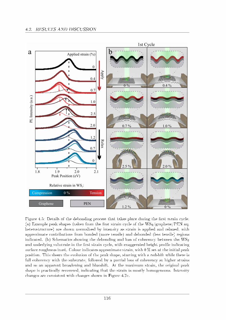
4.2. RESULTS AND DISCUSSION
2.5
0
1.2
2.0
0.7
0.7
1.0
0
0.4
0.7 %
0 % 0.4 %
1.0 %
2.5 % 2.0 %
1.2 % 0 %
bApplied strain (%)a
Peak Position (eV)
PL
Inte
nsi
ty (
a.u.)
1.8 1.9 2.0 2.1
Graphene PEN
Relative strain in :WS2
Apply
Relax
1st Cycle
Compression 0 % Tension
Figure 4.5: Details of the debonding process that takes place during the �rst strain cycle.(a) Example peak shapes (taken from the �rst strain cycle of the WS2/graphene/PEN aq.heterostructure) are shown normalised by intensity as strain is applied and relaxed, withapproximate contributions from bonded (more tensile) and debonded (less tensile) regionsindicated. (b) Schematics showing the debonding and loss of coherency between the WS2and underlying substrate in the �rst strain cycle, with exaggerated height pro�le indicatingsurface roughness inset. Colour indicates approximate strain, with 0 % set at the initial peakposition. This shows the evolution of the peak shape, starting with a redshift while there isfull coherency with the substrate, followed by a partial loss of coherency at higher strainsand so an apparent broadening and blueshift. At the maximum strain, the original peakshape is practically recovered, indicating that the strain is mostly homogeneous. Intensitychanges are consistent with changes shown in Figure 4.7c.
116
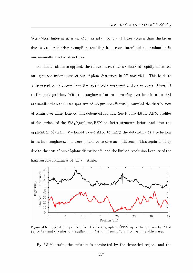
4.2. RESULTS AND DISCUSSION
WS2/MoS2 heterostructures. Our transition occurs at lower strains than the latter
due to weaker interlayer coupling, resulting from more interfacial contamination in
our manually stacked structures.
As further strain is applied, the relative area that is debonded rapidly increases,
owing to the unique ease of out-of-plane distortion in 2D materials. This leads to
a decreased contribution from the redshifted component and so an overall blueshift
to the peak position. With the roughness features occurring over length scales that
are smaller than the laser spot size of ∼6 µm, we e�ectively sampled the distribution
of strain over many bonded and debonded regions. See Figure 4.6 for AFM pro�les
of the surface of the WS2/graphene/PEN aq. heterostructure before and after the
application of strain. We hoped to use AFM to image the debonding as a reduction
in surface roughness, but were unable to resolve any di�erence. This again is likely
due to the ease of out-of-plane distortions,[7] and the limited resolution because of the
high surface roughness of the substrate.
0
10
20
30
40
Hei
ght
(nm
)
0 5 10 15 20 25 30 35
0
10
20
30
40
Position (µm)
Unst
rain
edS
trai
ned
Figure 4.6: Typical line pro�les from the WS2/graphene/PEN aq. surface, taken by AFM(a) before and (b) after the application of strain, from di�erent but comparable areas.
By 2.5 % strain, the emission is dominated by the debonded regions and the
117

4.2. RESULTS AND DISCUSSION
initial peak shape is mostly recovered, with a smaller redshift due to the partial
strain transfer. The transition can be best observed with reference to the changes
in the global peak position (Figure 4.7a) and full-width half-maximum (FWHM)
(Figure 4.7b), where there is a marked change above 0.4 % strain, with a partial
reversal of the initially strong redshift and a broadening of the PL peak width. The
cause of the increase in standard error at the onset of coherency loss is the inherent
random nature of the debonding, which leads to di�erent domains losing coherency at
di�erent rates. In Figure 4.7a we also plot the the value of �0.19 eV/% strain predicted
by Su et al.[31] for bandgap changes in WS2 under tensile strain, indicating that even
before coherency loss the WS2 experiences less than half of the strain applied to the
substrate. This is a result of the measurement geometry and the mismatch of Young's
moduli between the �lm and the substrate. See Section 3.6 and Figure 3.5a for more
information.[32]
On the basis that the WS2 experiences 50 % of the applied strain at the point
debonding begins to occur (a value of 0.35 % strain in the WS2), it is possible to
estimate the shear stress necessary for debonding to take place. Using Equation 3.8
(as derived in Section 3.6) with the average distance from the edge x = 20 μm and
the Young's modulus E f = 270 GPa,[33] the interfacial shear stress is estimated to be
τf = 28 kPa. While this is valid as a �rst approximation, the assumption of a planar
interface likely causes underestimation of the true value due to stress concentrations
in the valleys of the substrate surface seen in practice (Figure 4.6).[34] This analysis
also implies that the onset of debonding progresses rapidly across the domain, moving
at a rate of ∼50 μm/% strain.
118

4.2. RESULTS AND DISCUSSION
0.0 0.5 1.0 1.5 2.0 2.5
1.92
1.94
1.96
1.98
2.00
PL
Pea
k P
osi
tion
(eV
)
Strain (%)0.0 0.5 1.0 1.5 2.0 2.5
40
50
70
80
90
100
110
FW
HM
(eV
)m
Strain (%)
1st
2nd
3rd
4th
RelaxApply
Pre transferTheory
Apply
Relax
a b
0 %
2.5 % 0 %
1.6 %
Apply
Peak Position (eV)
PL
Inte
nsi
ty (
a.u.)
1.8 1.9 2.0 2.1
Strain (%)
00.71.62.5
0 %
2.5 % 0 %
1.6 %
dc
Relative strain in WS2
Compression 0 % Tension
2nd Cycle
Figure 4.7: Changes in the peak position and shape, and details of the stabilised strainbehaviour in subsequent strain cycles after debonding. (a) Overall peak position and (b)FWHM for the WS2/graphene/PEN non-aq. heterostructure over 3 strain cycles, and beforetransfer. Pre-transfer values, the shift predicted by theory, and standard errors are alsoindicated. The inset in (a) shows the small relaxation/blueshift that occurs between straincycles. (c) Changes in the peak position and intensity as strain is applied. Note no majorchanges in peak shape over full range of strain, indicating that a stable state has beenreached. (d) Schematics showing the e�ect of strain on the WS2 in the second strain cycleas a result of the debonding in the �rst cycle, with exaggerated height pro�le inset. Colourindicates approximate strain, with 0 % set at the initial peak position.
Figure 4.7c shows the changes to the emission during the second strain cycle. As
the WS2 has largely debonded from the underlying substrate, the degree of strain
transfer and so the magnitude of the redshift is smaller, and the strain distribution is
119
4.2. RESULTS AND DISCUSSION
largely homogeneous, as re�ected in the more modest broadening. Two mechanisms
contribute to the associated increase in luminescence intensity. Firstly, an increase in
the absorbance cross-section as the bandgap narrows leads to more incident light being
absorbed. Secondly, due to the increasingly large o�set between the K (direct, radi-
ative) and∑
(indirect, non-radiative) conduction band minima as strain increases,
there is a reduction in the quenching caused by the drain of carriers from K to∑; this
draining occurs since the∑
minimum is lowered in energy due to bandgap renormal-
isation caused by the high density of optically generated excitons.[18] We believe that
the expected quenching at higher strains is not observed due to the incomplete strain
transfer, though if some parts of the WS2 are above the expected threshold where
the intensity begins to decrease again while others are below, this would explain the
relatively modest PL intensity enhancement we observe compared to that predicted
by Steinho� et al. for MoS2.[18]
With reference to our recent KPM study on the WS2/graphene/PEN non-aq.
heterostructure, we propose that the debonding is primarily between the substrate
and the �rst layer of 2D materials, but cannot comprehensively rule out debonding
between layers of 2D materials. This study indicated a debonding transition at similar
strains in the PL peak position (Figure 4.8a) and work function (Figure 4.8b), with
only slight discrepancies in the changes to the work function of graphene and WS2,
implying that the e�ect happens nearly simultaneously in both materials.[28]
Further strain cycling reveals stabilisation to a hysteresis loop, in which the de-
bonding and interfacial sliding lead to incomplete strain transfer (Figure 4.7a). This
is in contrast to the �ndings of Liu et al.,[6] who observed no hysteresis in their meas-
120

4.2. RESULTS AND DISCUSSION
0.0 0.5 1.0
1.92
1.94
1.96
1.98
PL
Pea
k P
osi
tion
(eV
)
Strain (%)
1.90 Graphene
WS2
4.6
4.7
4.8
4.9
Work
Fun
ctio
n (
eV)
0.0 0.4 0.8 1.2Strain (%)
1.6
a b
Figure 4.8: Comparison of debonding observed in PL and KPM measurements ofWS2/graphene/PEN non-aq. heterostructure. (a) PL peak position from WS2 and (b) workfunction from graphene and WS2. Note transition at similar applied strain (∼1 %) in bothcases, implying that debonding takes place predominantly at the interface with PEN. This�gure is adapted from Sarwat et al.[28]
urements of strained MoS2 on PDMS, though they observed a similar incomplete
strain transfer. This hysteresis originates from the compressive strain in the WS2
once the substrate strain is relaxed, a result of the partial relaxation of tensile strain
in the WS2 following the debonding as strain was applied. Over time, this compress-
ive strain relaxes and the heterostructure partially reconforms with the substrate,
leading to the small redshift highlighted in the inset of Figure 4.7a. When the sub-
strate is subsequently strained again, the initial uptake of the strain is lower than in
the �rst strain cycle and decreases further at higher strains. The reverse is true as
the strain is relaxed, initially blueshifting the spectrum more rapidly before levelling
o� as substrate strain approaches zero.
To validate the debonding mechanism, we conducted local mapping of the peak
positions during the same strain cycling described above on the WS2/graphene/PEN
non-aq. heterostructure, and compared this to the mapping of the same hetero-
121

4.2. RESULTS AND DISCUSSION
structure with a 50 ± 5 nm poly(methyl methacrylate) (PMMA) coating applied
to the PEN surface to modify the surface roughness. The roughness of the PEN and
PMMA/PEN substrates was characterised by AFM (Figure 4.9a�4.9c), and found to
be Rq = 6.89 ± 1 nm for PEN and Rq = 9.49 ± 1 nm for PMMA/PEN. The PMMA
�lm thickness was measured by cross-sectional SEM, an example of which is shown
in Figure 4.9d.
PEN
PMMA/PEN
RMS Roughness (nm)
Area1
Area2
Area3
Area4
Area5
Avg.
5.03 8.32 7.57 6.16 7.37 6.89± 1
8.88 9.24 9.00 10.0710.27 9.49± 1
c
0
20
40
60
80
100
120
140
Height(nm)
5 µm 5 µm
PMMA
SiO2
1 µm
a b
d
Figure 4.9: Characterisation of the surface topography and roughness for the PEN substratewith and without PMMA coating. Example AFM images taken on PEN (a) without and(b) with a layer of A1 495K PMMA spin coated onto the surface (scale bar 5 µm), and(c) a table summarising the RMS roughness values of multiple line pro�les take from both.(d) Example of a cross-sectional SEM image used in determining the �lm thickness of the50 ± 5 nm PMMA layer deposited onto a silicon wafer with 300 nm oxide layer by the sameparameters. Scale bar is 1 µm.
To transfer onto the PMMA/PEN substrate, some modi�cations to the standard
122

4.2. RESULTS AND DISCUSSION
procedure were required, since the PMMA layer precluded the use of acetone. By
�rst transferring the WS2 onto the graphene by aqueous methods, the entire hetero-
structure could then be transferred in a single step using a sca�old composed of the
IPA soluble photoresist ma-N 1420 (Micro Resist). While this �lm was found to be
more fragile than the usual PMMA sca�old, su�cient regions withstood the transfer
to be measured.
In the �rst strain cycle, we observed small variations over the area we examined
for the structure without PMMA (Figure 4.10a) and larger variations in the structure
with PMMA (Figure 4.11a), in accordance with the increase in roughness. The later
and broader onset of debonding in the PMMA structure is caused by the lower degree
of strain transfer from the substrate through the softer PMMA layer (cf. Figure 4.10c
& 4.11c). This is also the reason for the observed smaller total peak shift in this
structure. After debonding has taken place, the e�ect of the di�ering roughness
values is reduced (cf. Figure 4.10d & 4.11d), though the degree of hysteresis during
strain cycling is larger with PMMA. The debonding is accompanied by a reduction
in the spread of the peak positions in both cases (cf. Figure 4.10e & 4.10f, and 4.11e
& 4.11f). In Figure 4.11g we also illustrate line pro�les taken before and after the
application of strain in the �rst cycle, revealing a quasiperiodic distribution that is
globally redshifted but is otherwise largely una�ected by strain. This likely indicates
a dependence on the larger scale variations of the substrate surface which remains
signi�cant even at the maximum applied strain of 2.5 %.
123
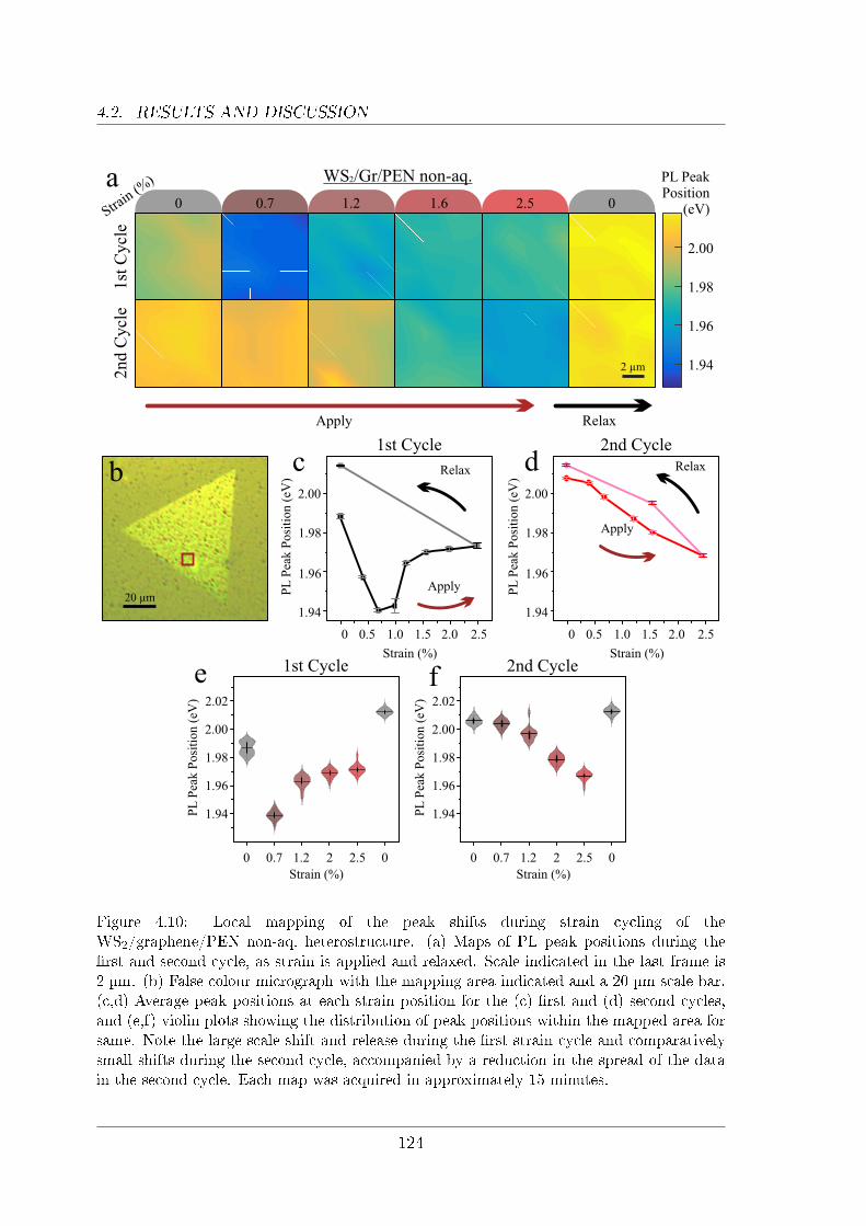
4.2. RESULTS AND DISCUSSION
Strain (%)
PL
Pea
k P
osi
tion (
eV)
0 0.7 1.2 2 2.5 0
1.94
1.96
1.98
2.00
2.02
0 0.5 1.0 1.5 2.0 2.5
Strain (%)
1.94
1.96
1.98
2.00
PL
Pea
k P
osi
tion (
eV)
Apply
Relax
1.94
1.96
1.98
2 µm
0 0.7 1.2 1.6 2.5 0
1st
Cycl
e2nd C
ycl
e
Apply Relax
PL PeakPosition
(eV)
a
c d
1.94
1.96
1.98
2.00
20 µm
Strain (%)
PL
Pea
k P
osi
tion (
eV)
0 0.7 1.2 2 2.5 0
1.94
1.96
1.98
2.00
2.02
0 0.5 1.0 1.5 2.0 2.5
Strain (%)
Apply
Relax
1.94
1.96
1.98
2.00
PL
Pea
k P
osi
tion (
eV)
1st Cycle 2nd Cycle
1st Cycle 2nd Cycle
b
e f
Strain
(%) WS /Gr/PEN non-aq.2
Figure 4.10: Local mapping of the peak shifts during strain cycling of theWS2/graphene/PEN non-aq. heterostructure. (a) Maps of PL peak positions during the�rst and second cycle, as strain is applied and relaxed. Scale indicated in the last frame is2 µm. (b) False colour micrograph with the mapping area indicated and a 20 µm scale bar.(c,d) Average peak positions at each strain position for the (c) �rst and (d) second cycles,and (e,f) violin plots showing the distribution of peak positions within the mapped area forsame. Note the large scale shift and release during the �rst strain cycle and comparativelysmall shifts during the second cycle, accompanied by a reduction in the spread of the datain the second cycle. Each map was acquired in approximately 15 minutes.
124
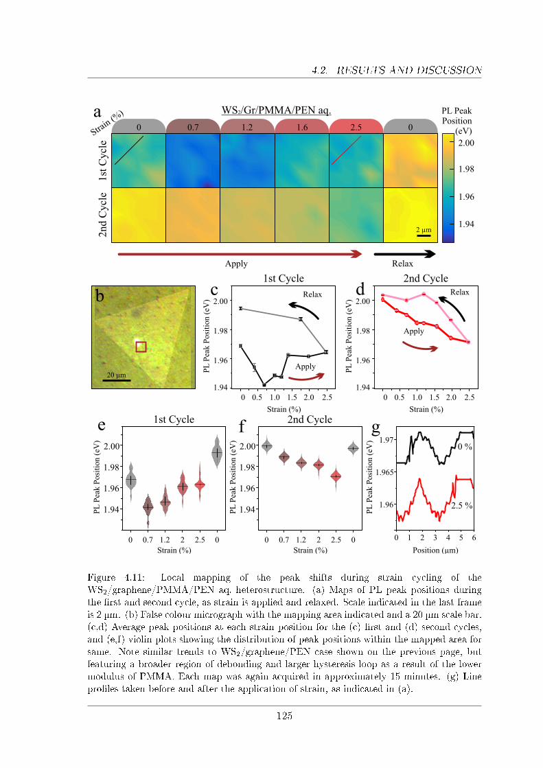
4.2. RESULTS AND DISCUSSION
Strain (%)
PL
Pea
k P
osi
tion (
eV)
0 0.7 1.2 2 2.5 0
1.94
1.96
1.98
2.00
0 0.5 1.0 1.5 2.0 2.5
Strain (%)
PL
Pea
k P
osi
tion (
eV)
Apply
Relax
1.96
1.94
1.98
2.00
0 0.7 1.2 1.6 2.5 0Stra
in(%
)
1st
Cycl
e2nd C
ycl
e
Apply Relax
PL PeakPosition
(eV)
a
c d
1.94
1.96
1.98
2.00
20 µm
Strain (%)
PL
Pea
k P
osi
tion (
eV)
0 0.7 1.2 2 2.5 0
1.94
1.96
1.98
2.00
0 0.5 1.0 1.5 2.0 2.5
Strain (%)
PL
Pea
k P
osi
tion (
eV)
1.96
1.94
1.98
2.00
Apply
Relax
1st Cycle 2nd Cycle
1st Cycle 2nd Cycle
b
e f
2 µm
WS /Gr/PMMA/PEN aq.2
1 2 3 4 5 6
1.96
1.97
0
1.965
PL
Pea
k P
osi
tion (
eV)
Position (µm)
g0 %
2.5 %
Figure 4.11: Local mapping of the peak shifts during strain cycling of theWS2/graphene/PMMA/PEN aq. heterostructure. (a) Maps of PL peak positions duringthe �rst and second cycle, as strain is applied and relaxed. Scale indicated in the last frameis 2 µm. (b) False colour micrograph with the mapping area indicated and a 20 µm scale bar.(c,d) Average peak positions at each strain position for the (c) �rst and (d) second cycles,and (e,f) violin plots showing the distribution of peak positions within the mapped area forsame. Note similar trends to WS2/graphene/PEN case shown on the previous page, butfeaturing a broader region of debonding and larger hysteresis loop as a result of the lowermodulus of PMMA. Each map was again acquired in approximately 15 minutes. (g) Linepro�les taken before and after the application of strain, as indicated in (a).
125
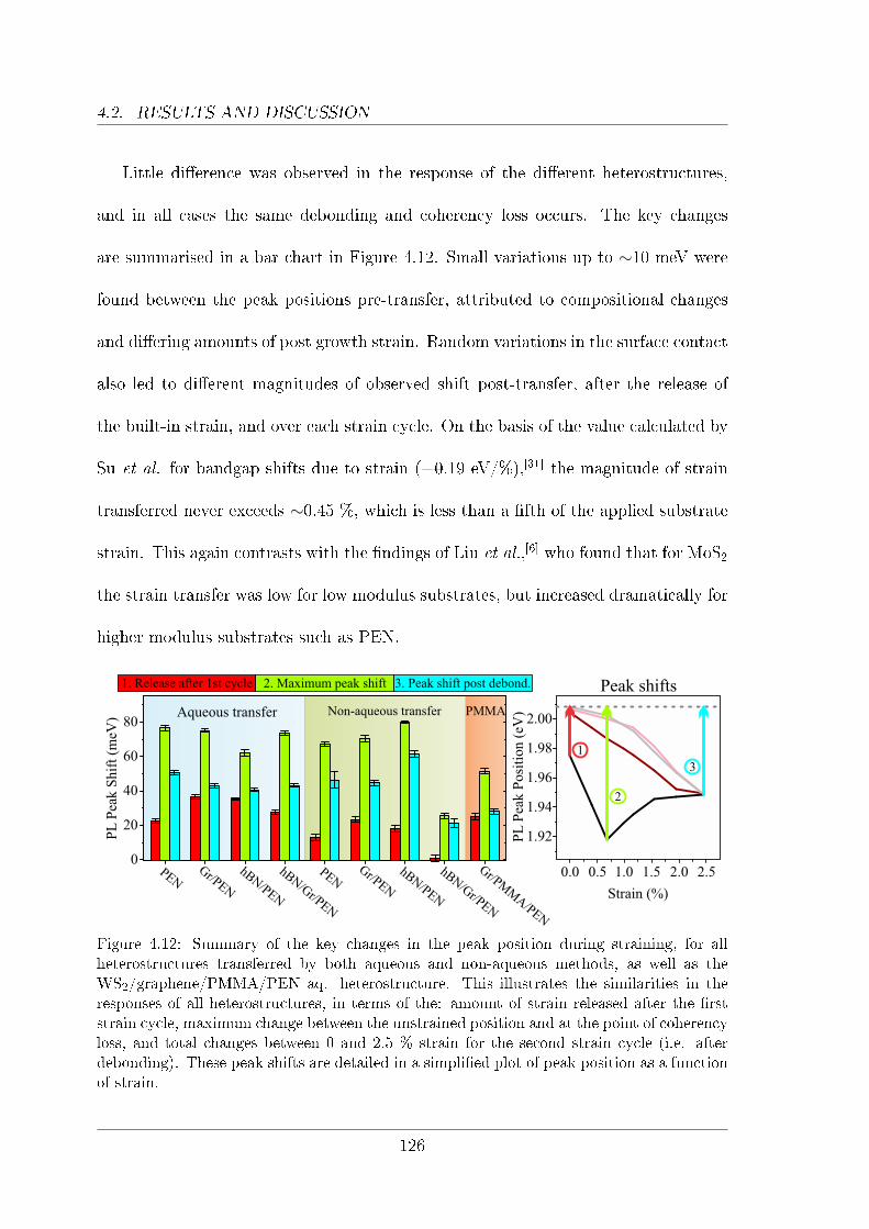
4.2. RESULTS AND DISCUSSION
Little di�erence was observed in the response of the di�erent heterostructures,
and in all cases the same debonding and coherency loss occurs. The key changes
are summarised in a bar chart in Figure 4.12. Small variations up to ∼10 meV were
found between the peak positions pre-transfer, attributed to compositional changes
and di�ering amounts of post growth strain. Random variations in the surface contact
also led to di�erent magnitudes of observed shift post-transfer, after the release of
the built-in strain, and over each strain cycle. On the basis of the value calculated by
Su et al. for bandgap shifts due to strain (=0.19 eV/%),[31] the magnitude of strain
transferred never exceeds ∼0.45 %, which is less than a �fth of the applied substrate
strain. This again contrasts with the �ndings of Liu et al.,[6] who found that for MoS2
the strain transfer was low for low modulus substrates, but increased dramatically for
higher modulus substrates such as PEN.
PENG
r/PEN
hBNPEN/
h
Gr
BN
PEN
//
PENG
r/PEN
hBNPEN/
h
Gr
BN
PEN
//
Aqueous transfer Non-aqueous transfer
1. Release after 1st cycle 2. Maximum peak shift 3. Peak shift post debond.
PL
Pea
k S
hif
t (m
eV)
0
20
40
60
80
Gr/
/
PMM
APEN
PMMA
Strain (%)
0.0 0.5 1.0 1.5 2.0 2.5
1.92
1.94
1.96
1.98
2.00
PL
Pea
kP
osi
tion
(eV
)
1
2
3
Peak shifts
Figure 4.12: Summary of the key changes in the peak position during straining, for allheterostructures transferred by both aqueous and non-aqueous methods, as well as theWS2/graphene/PMMA/PEN aq. heterostructure. This illustrates the similarities in theresponses of all heterostructures, in terms of the: amount of strain released after the �rststrain cycle, maximum change between the unstrained position and at the point of coherencyloss, and total changes between 0 and 2.5 % strain for the second strain cycle (i.e. afterdebonding). These peak shifts are detailed in a simpli�ed plot of peak position as a functionof strain.
126
4.2. RESULTS AND DISCUSSION
To study the time-dependent redshift that occurs between measurements, we chose
the WS2/hBN/PEN aq. heterostructure as an example in an attempt to control
other possible in�uences on the properties from electronic e�ects, since hBN has been
shown to behave as an excellent screening layer when used as a substrate for other
2D materials.[35,36] PL measurements were performed over the course of several hours
at regular intervals, after holding the substrate at 2.5 % strain and then returning to
zero. This con�rmed that a residual blueshift remained after the substrate strain was
relaxed. As described above, the blueshift following the �rst strain cycle can only be
partially recovered following the removal of the substrate strain, due to the release of
the built-in tensile strain arising from the transfer process (Figure 4.13a). After the
second strain cycle, the magnitude of blueshift is signi�cantly smaller (Figure 4.13b).
By annealing the structure at the glass transition temperature of the substrate
(PEN T g = 120 °C), we found that the emission was blue shifted, and the peak
slightly sharpened (Figure 4.13c & 4.13d). This can be explained by an increase in
the coherency between the substrate and WS2 leading to a slight compressive strain
as the debonded regions �atten out. The sharpening of the peak is caused by an
increase in the homogeneity of the strain, and was stable over the time measured.
To demonstrate the resilience of these structures, after annealing we repeated the
strain cycling up to 200 times, measuring the PL response at several intervals. This
shows the stability of the response, in terms of the peak position�barring strain re-
laxation e�ects�as well as the FWHM and PL intensity (Figure 4.13e�4.13g). To
ensure consistency between measurements, all spectra were taken one hour after the
strain cycling was performed, limiting the in�uence of the previously described re-
127
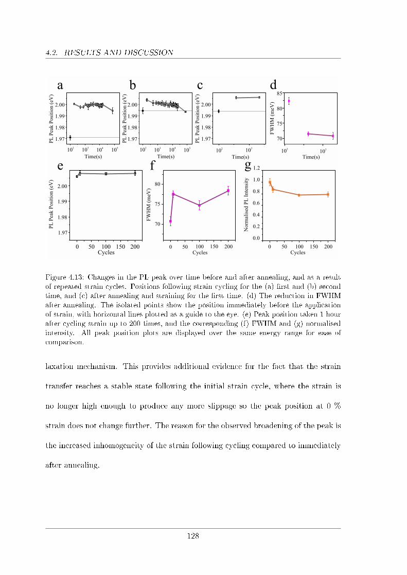
4.2. RESULTS AND DISCUSSION
102
103
104
105
PL
Pea
k P
osi
tion (
eV)
Time(s)
PL
Pea
k P
osi
tion
(eV
)
Time(s)
a b
1.97
1.98
1.99
2.00
102
103
104
105
1.97
1.98
1.99
2.00
g
0 50 100 150 200
0.0
0.2
0.4
0.6
0.8
1.0
1.2
Norm
alis
edIn
tensi
tyP
L
Cycles0 50 100 150 200
PL
Pea
k P
osi
tion
(eV
)
Cycles0 50 100 150 200
70
75
80
FW
HM
(meV
)
Cycles
e f
1.97
1.98
1.99
2.00
103
FW
HM
(meV
)
PL
Pea
k P
osi
tion
(eV
)
Time(s)
d
70
75
80
85
c
102
Time(s)10
2
103
1.97
1.98
1.99
2.00
Figure 4.13: Changes in the PL peak over time before and after annealing, and as a resultof repeated strain cycles. Positions following strain cycling for the (a) �rst and (b) secondtime, and (c) after annealing and straining for the �rst time. (d) The reduction in FWHMafter annealing. The isolated points show the position immediately before the applicationof strain, with horizontal lines plotted as a guide to the eye. (e) Peak position taken 1 hourafter cycling strain up to 200 times, and the corresponding (f) FWHM and (g) normalisedintensity. All peak position plots are displayed over the same energy range for ease ofcomparison.
laxation mechanism. This provides additional evidence for the fact that the strain
transfer reaches a stable state following the initial strain cycle, where the strain is
no longer high enough to produce any more slippage so the peak position at 0 %
strain does not change further. The reason for the observed broadening of the peak is
the increased inhomogeneity of the strain following cycling compared to immediately
after annealing.
128
4.3. CONCLUSIONS
4.3 Conclusions
In summary, we have demonstrated a mechanism by which the expected incomplete
strain transfer to 2D materials on �exible PEN substrates takes place, broadly inde-
pendently of the di�erent heterostructure con�gurations and fabrication techniques
used. These �ndings serve to illustrate that for 2D heterostructures to be used in
�exible electronics, careful control of the processing will be required in order to avoid
the unstable behaviour we have observed to varying degrees across all of the di�erent
structures studied. Since the debonding transition occurs within what we consider to
be the useful operating strain range, this suggests the need for extra processing steps
to release the built-in tensile strain arising from the fabrication process to produce
stable and consistent behaviour across multiple devices. However, the demonstration
of stable behaviour following the initial debonding is encouraging, as this indicates
that after an initial `preconditioning' strain cycle the properties of the heterostruc-
tures are consistent, and as such would be suitable for service.
4.4 Acknowledgements
AFM mapping of the PEN and PMMA/PEN surface was carried out by Miss Nicola
Flanagan, and AFM and KPM of the strained heterostructures was performed by
Mr Syed Ghazi Sarwat. The majority of the 2D materials used here were grown by
the author, but occasionally materials were provided by: Dr Yuewen Sheng (WS2,
graphene), Miss Linlin Hou (WS2), and Miss Wenshuo Xu (hBN).
129

Bibliography
[1] H. Zhang, �Ultrathin Two-Dimensional Nanomaterials�, ACS Nano 2015, 9,9451�9469.
[2] X. Zhang, Z. Shao, X. Zhang, Y. He, J. Jie, �Surface Charge Transfer Dopingof Low-Dimensional Nanostructures toward High-Performance Nanodevices�,Advanced Materials 2016, 28, 10409�10442.
[3] P. Johari, V. B. Shenoy, �Tuning the Electronic Properties of SemiconductingTransition Metal Dichalcogenides by Applying Mechanical Strains�, ACS Nano2012, 6, 5449�5456.
[4] Y. Wang, C. Cong, W. Yang, J. Shang, N. Peimyoo, Y. Chen, J. Kang, J.Wang, W. Huang, T. Yu, �Strain-Induced Direct-Indirect Bandgap Transitionand Phonon Modulation in Monolayer WS2�, Nano Res. 2015, 8, 2562�2572.
[5] Y. He, Y. Yang, Z. Zhang, Y. Gong, W. Zhou, Z. Hu, G. Ye, X. Zhang, E.Bianco, S. Lei, Z. Jin, X. Zou, Y. Yang, Y. Zhang, E. Xie, J. Lou, B. I.Yakobson, R. Vajtai, B. Li, P. M. Ajayan, �Strain Induced Electronic StructureChanges in Stacked van der Waals Heterostructures�, Nano Letters 2016, 16,3314�3320.
[6] Z. Liu, M. Amani, S. Najmaei, Q. Xu, X. Zou, W. Zhou, T. Yu, C. Qiu, A. G.Birdwell, F. J. Crowne, R. Vajtai, B. I. Yakobson, Z. Xia, M. Dubey, P. M.Ajayan, J. Lou, �Strain and Structure Heterogeneity in MoS2 Atomic LayersGrown by Chemical Vapour Deposition�, Nature Communications 2014, 5,5246.
[7] C. Lee, Q. Li, W. Kalb, X.-Z. Liu, H. Berger, R. W. Carpick, J. Hone, �Fric-tional Characteristics of Atomically Thin Sheets�, Science 2010, 328, 76�80.
[8] S. Li, Q. Li, R. W. Carpick, P. Gumbsch, X. Z. Liu, X. Ding, J. Sun, J. Li,�The Evolving Quality of Frictional Contact with Graphene�, Nature 2016,539, 541�546.
[9] Teijin DuPont Films, Teonex Q51: Wilton, UK, Jul 21, 2006, http://www.iec-international.com/pdf/pen_teonexq51.pdf (visited on30/10/2018).
[10] J. E. Lee, G. Ahn, J. Shim, Y. S. Lee, S. Ryu, �Optical separation of mechanicalstrain from charge doping in graphene�, Nat. Commun. 2012, 3, 1024.
130
[11] Y. Sheng, W. Xu, X. Wang, Z. He, Y. Rong, J. H. Warner, �Mixed MultilayeredVertical Heterostructures Utilizing Strained Monolayer WS2�, Nanoscale 2016,8, 2639�2647.
[12] H.-s. Kim, Ph.D Thesis, University of Illinois, Urbana, IL, USA, 2011, p. 172.
[13] W. Zhao, Z. Ghorannevis, K. K. Amara, J. R. Pang, M. Toh, X. Zhang, C.Kloc, P. H. Tan, G. Eda, �Lattice Dynamics in Mono- and Few-Layer Sheetsof WS2 and WSe2�, Nanoscale 2013, 5, 9677�9683.
[14] E. J. Heller, Y. Yang, L. Kocia, W. Chen, S. Fang, M. Borunda, E. Kaxiras,�Theory of Graphene Raman Scattering�, ACS Nano 2016, 10, 2803�2818.
[15] R. V. Gorbachev, I. Riaz, R. R. Nair, R. Jalil, L. Britnell, B. D. Belle, E. W.Hill, K. S. Novoselov, K. Watanabe, T. Taniguchi, A. K. Geim, P. Blake,�Hunting for Monolayer Boron Nitride: Optical and Raman Signatures�, Small2011, 7, 465�468.
[16] T. Ohta, A. Bostwick, T. Seyller, K. Horn, E. Rotenberg, �Controlling theElectronic Structure of Bilayer Graphene�, Science 2006, 313, 951�954.
[17] A. A. Mitioglu, P. Plochocka, J. N. Jadczak, W. Esco�er, G. L. J. A. Rikken,L. Kulyuk, D. K. Maude, �Optical Manipulation of the Exciton Charge Statein Single-Layer Tungsten Disul�de�, Physical Review B - Condensed Matterand Materials Physics 2013, 88, 245403.
[18] A. Steinho�, J. H. Kim, F. Jahnke, M. Rösner, D. S. Kim, C. Lee, G. H. Han,M. S. Jeong, T. O. Wehling, C. Gies, �E�cient Excitonic Photoluminescence inDirect and Indirect Band Gap Monolayer MoS2�, Nano Lett. 2015, 15, 6841�6847.
[19] T. Nagai, T. J. Inagaki, Y. Kanemitsu, �Band-gap renormalization in highlyexcited GaN�, Applied Physics Letters 2004, 84, 1284�1286.
[20] A. Castellanos-Gomez, M. Barkelid, A. M. Goossens, V. E. Calado, H. S. J.Van Der Zant, G. A. Steele, �Laser-Thinning of MoS2: On Demand Generationof a Single-Layer Semiconductor�, Nano Letters 2012, 12, 3187�3192.
[21] S. Najmaei, Z. Liu, P. M. Ajayan, J. Lou, �Thermal E�ects on the Charac-teristic Raman Spectrum of Molybdenum Disul�de (MoS2) of Varying Thick-nesses�, Applied Physics Letters 2012, 100, 013106.
[22] C. E. Giusca, I. Rungger, V. Panchal, C. Melios, Z. Lin, Y. C. Lin, E. Kahn,A. L. Elías, J. A. Robinson, M. Terrones, O. Kazakova, �Excitonic E�ects inTungsten Disul�de Monolayers on Two-Layer Graphene�, ACS Nano 2016,10, 7840�7846.
[23] K. F. Mak, K. He, C. Lee, G. H. Lee, J. Hone, T. F. Heinz, J. Shan, �TightlyBound Trions in Monolayer MoS2�, Nat. Mater. 2013, 12, 207�211.
[24] M. L. Trolle, T. G. Pedersen, V. Véniard, �Model Dielectric Function for 2DSemiconductors Including Substrate Screening�, Scienti�c Reports 2017, 7,39844.
131

[25] K. He, C. Poole, K. F. Mak, J. Shan, �Experimental Demonstration of Continu-ous Electronic Structure Tuning via Strain in Atomically Thin MoS2�, NanoLett. 2013, 13, 2931�2936.
[26] M.-Y. Tsai, A. Tarasov, Z. R. Hesabi, H. Taghinejad, P. M. Campbell, C. A.Joiner, A. Adibi, E. M. Vogel, �Flexible MoS2 Field-E�ect Transistors for Gate-Tunable Piezoresistive Strain Sensors�, ACS Applied Materials & Interfaces2015, 7, 12850�12855.
[27] N. Harada, S. Sato, N. Yokoyama, �Computational Study on Electrical Proper-ties of Transition Metal Dichalcogenide Field-E�ect Transistors with StrainedChannel�, Journal of Applied Physics 2014, 115, 034505.
[28] S. G. Sarwat, M. Tweedie, B. F. Porter, Y. Zhou, Y. Sheng, J. Mol, J. Warner,H. Bhaskaran, �Revealing Strain-Induced E�ects in Ultrathin Heterostructuresat the Nanoscale�, Nano Letters 2018, 18, 2467�2474.
[29] H. Kumar, L. Dong, V. B. Shenoy, �Limits of Coherency and Strain Transferin Flexible 2D van der Waals Heterostructures: Formation of Strain Solitonsand Interlayer Debonding�, Scienti�c Reports 2016, 6, 21516.
[30] S. Susarla, P. Manimunda, Y. Morais Jaques, J. A. Hachtel, J. C. Idrobo,S. A. Syed Amnulla, D. S. Galvão, C. S. Tiwary, P. M. Ajayan, �DeformationMechanisms of Vertically Stacked WS2/MoS2 Heterostructures: The Role ofInterfaces�, ACS Nano 2018, 12, 4036�4044.
[31] L. Su, Y. Yu, L. Cao, Y. Zhang, �E�ects of Substrate Type and Material-Substrate Bonding on High-Temperature Behavior of Monolayer WS2�, NanoResearch 2015, 8, 2686�2697.
[32] D. Hull, T. W. Clyne in An Introduction to Composite Materials, 1996.
[33] S. Bertolazzi, J. Brivio, A. Kis, �Stretching and Breaking of Ultrathin MoS2�,ACS Nano 2011, 5, 9703�9709.
[34] E. D. Reedy Jr., �Tensile Cracking of a Brittle Conformal Coating on a RoughSubstrate�, International Journal of Fracture 2016, 199, 245�250.
[35] P. Rivera, J. R. Schaibley, A. M. Jones, J. S. Ross, S. Wu, G. Aivazian, P.Klement, K. Seyler, G. Clark, N. J. Ghimire, J. Yan, D. G. Mandrus, W.Yao, X. Xu, �Observation of Long-Lived Interlayer Excitons in MonolayerMoSe2/WSe2 Heterostructures�, Nature Communications 2015, 6, 6242.
[36] Y. Tan, L. Ma, Z. Gao, M. Chen, F. Chen, �Two-Dimensional Heterostructureas a Platform for Surface-Enhanced Raman Scattering�, Nano Letters 2017,17, 2621�2626.
132
Chapter 5
All-2D Transparent Photodetector
Arrays on Flexible Substrates
5.1 Introduction
In Chapter 4, we described the formation of heterostructures on �exible poly(ethylene
naphthalate) (PEN) substrates, and discussed a mechanism by which tensile strain is
accommodated in 2D materials during substrate bending. We concluded by discussing
the possible rami�cations of this debonding mechanism for the fabrication of �exible
devices. The initial instability of the behaviour suggested that further processing
would likely be necessary; the stabilisation apparent from the second strain cycle, as
well as the universality of the mechanism across all heterostructures, encouraged us
that this would not be especially challenging.
This chapter details the fabrication of transparent graphene�WS2�graphene lat-
eral heterostructured photodetectors on PEN substrates, devices that contain two
133
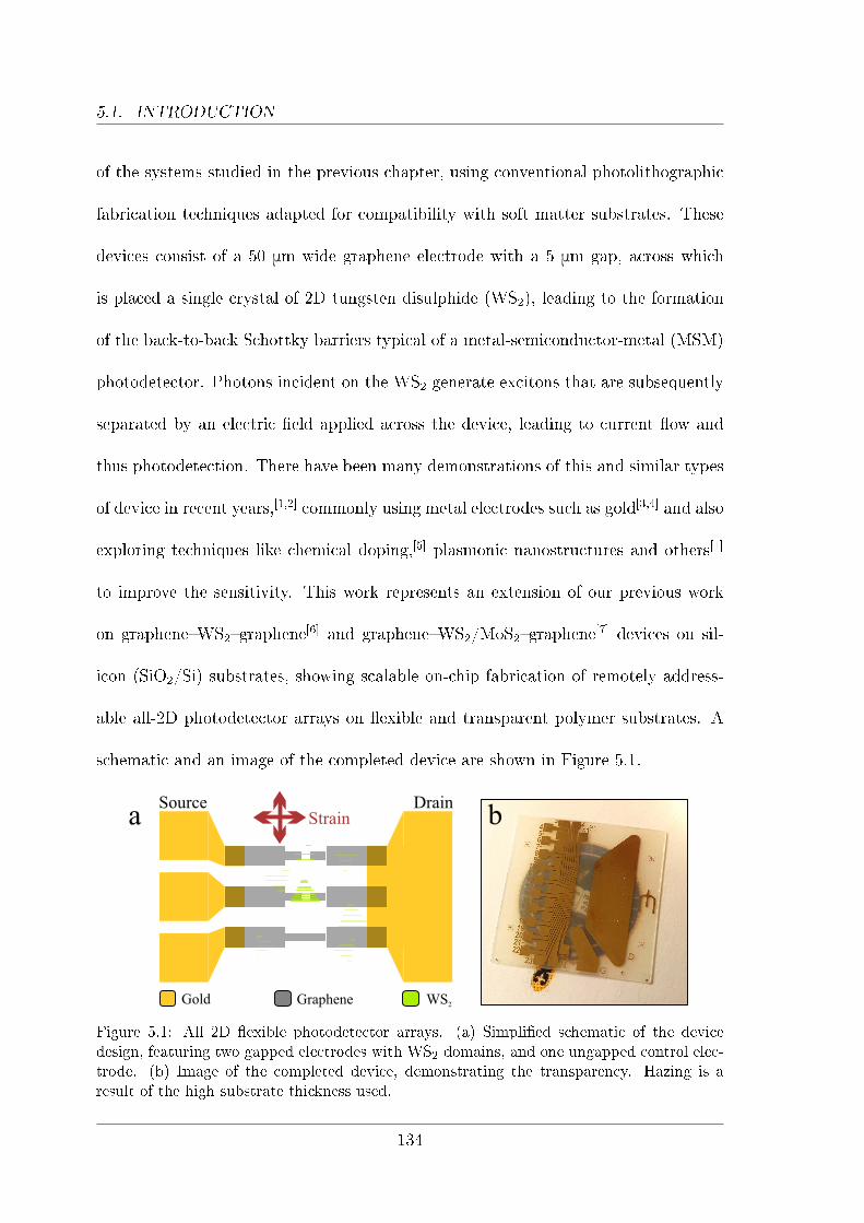
5.1. INTRODUCTION
of the systems studied in the previous chapter, using conventional photolithographic
fabrication techniques adapted for compatibility with soft matter substrates. These
devices consist of a 50 μm wide graphene electrode with a 5 μm gap, across which
is placed a single crystal of 2D tungsten disulphide (WS2), leading to the formation
of the back-to-back Schottky barriers typical of a metal-semiconductor-metal (MSM)
photodetector. Photons incident on the WS2 generate excitons that are subsequently
separated by an electric �eld applied across the device, leading to current �ow and
thus photodetection. There have been many demonstrations of this and similar types
of device in recent years,[1,2] commonly using metal electrodes such as gold[3,4] and also
exploring techniques like chemical doping,[5] plasmonic nanostructures and others[1]
to improve the sensitivity. This work represents an extension of our previous work
on graphene�WS2�graphene[6] and graphene�WS2/MoS2�graphene[7] devices on sil-
icon (SiO2/Si) substrates, showing scalable on-chip fabrication of remotely address-
able all-2D photodetector arrays on �exible and transparent polymer substrates. A
schematic and an image of the completed device are shown in Figure 5.1.
Gold Graphene WS2
Source DrainStraina b
Figure 5.1: All 2D �exible photodetector arrays. (a) Simpli�ed schematic of the devicedesign, featuring two gapped electrodes with WS2 domains, and one ungapped control elec-trode. (b) Image of the completed device, demonstrating the transparency. Hazing is aresult of the high substrate thickness used.
134

5.2. RESULTS AND DISCUSSION
Initial successes in fabrication using similar methods to those demonstrated pre-
viously were met with problems of device failure under strain. An analysis of the
failure mechanism led to the development and subsequent characterisation of a modi-
�ed lift-o� process for graphene patterning, to replace the traditional plasma etching
used initially. Though capable of slightly lower resolution, this technique produced
graphene of equivalent electrical quality to the �rst devices, while eliminating the
need for plasma etching entirely. This technique has the further advantage of po-
tentially facilitating patterning on top of existing structures with di�ering geometry,
impossible with plasma etching due to the requirement that each subsequent pattern
must contain the previous one if etching of the preceding layers is to be avoided.
Characterisation of these devices revealed that they too fail during the application of
strain, though in this case the exact nature of the failure mechanism remains unclear.
5.2 Results and Discussion
As even graphene is too delicate to be contacted directly, the �rst step in making
devices from 2D materials is the deposition of gold contacts to enable the connection
of source and drain electrodes. On silicon and other rigid substrates, a thin layer
of chromium or titanium is commonly deposited as an adhesion layer before the
deposition of the gold, due to the higher reactivity of these metals. This is important
as pure gold has very low peel resistance and, should the pattern even survive the
lift-o� process, the electrodes will quickly be damaged by the application of probes.[8]
This layer is very e�ective at promoting adhesion on SiO2 and should also be for PEN,
due to the formation of strong bonds with oxygen, in the latter case bonding to the
135
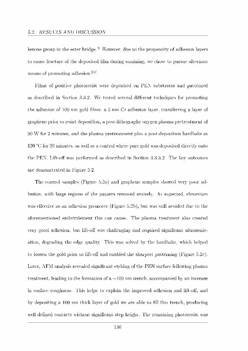
5.2. RESULTS AND DISCUSSION
ketone group in the ester bridge.[9] However, due to the propensity of adhesion layers
to cause fracture of the deposited �lm during straining, we chose to pursue alternate
means of promoting adhesion.[10]
Films of positive photoresist were deposited on PEN substrates and patterned
as described in Section 3.3.2. We tested several di�erent techniques for promoting
the adhesion of 100 nm gold �lms: a 5 nm Cr adhesion layer, transferring a layer of
graphene prior to resist deposition, a post-lithography oxygen plasma pretreatment of
90 W for 2 minutes, and the plasma pretreatment plus a post-deposition hardbake at
120 °C for 20 minutes, as well as a control where pure gold was deposited directly onto
the PEN. Lift-o� was performed as described in Section 3.3.3.2. The key outcomes
are demonstrated in Figure 5.2.
The control samples (Figure 5.2a) and graphene samples showed very poor ad-
hesion, with large regions of the pattern removed entirely. As expected, chromium
was e�ective as an adhesion promoter (Figure 5.2b), but was still avoided due to the
aforementioned embrittlement this can cause. The plasma treatment also created
very good adhesion, but lift-o� was challenging and required signi�cant ultrasonic-
ation, degrading the edge quality. This was solved by the hardbake, which helped
to loosen the gold prior to lift-o� and enabled the sharpest patterning (Figure 5.2c).
Later, AFM analysis revealed signi�cant etching of the PEN surface following plasma
treatment, leading to the formation of a ∼100 nm trench, accompanied by an increase
in surface roughness. This helps to explain the improved adhesion and lift-o�, and
by depositing a 100 nm thick layer of gold we are able to �ll this trench, producing
well de�ned contacts without signi�cant step height. The remaining photoresist was
136

5.2. RESULTS AND DISCUSSION
removed using acetone, and complete lift-o� was accomplished by up to 1 minute of
ultrasonication, followed by rinsing in isopropyl alcohol (IPA). This process is outlined
schematically in Figure 5.2d, and the full procedure is detailed in Section 3.3.3.
200 µm200 µm
a
1. Pattern photoresist 2. Plasma etching 3. Gold deposition 4. Ultrasonic lift-off
a b c
dS1813
PEN Au
Figure 5.2: Details of the fabrication process for gold contacts. (a�c) Post lift-o� opticalimages with pictures inset of (a) 100 nm Au with no adhesion layer or surface treatment, (b)95 nm Au with 5 nm Cr adhesion layer, (c) plasma treated substrate with hardbake. Scalebar in (a) is 200 μm. (d) Schematics of the �nal process for the formation of gold contactson PEN.
Films of graphene and domains of WS2 were grown by CVD. Due to the undesir-
ably high level of nucleation and consequent uneven surface morphology, we initially
turned our attention to improving the graphene growth process. As-rolled copper foil
has signi�cant surface striations that, along with grain boundaries, serve as nucleation
sites for graphene growth, leading to a reproduction of this texture in the graphene
�lm even after the growth substrate is removed.[11] To increase the homogeneity of
nucleation while decreasing its density, we trialled two forms of abrasive polishing: a
manual polish with Brasso® metal polish, and a two stage mechanical polish using
137

5.2. RESULTS AND DISCUSSION
stitched polishing mops with progressively �ner polishing compounds.
Polishing and growth were performed as described in Section 3.2.1. SEM images
of the graphene in each case are shown in Figure 5.3. Note the strongly striated
surface of the copper observed at low magni�cation in Figure 5.3a, visible as changes
in the contrast and direction of graphene ripples due to the texture of the copper.
The manual polish produced signi�cant improvement in the surface �nish, but some
scratches remain. We also found that despite signi�cant cleaning of the foil before
CVD was performed, some residual silica particles from the polish could be observed
on the surface (Figure 5.3b). Further improvement was possible with the mechanical
polish, which provided additional reduction in the appearance of scratches on the
surface of the foil (Figure 5.3c). Another advantage was that the foils were easier
to clean, likely due to the ready etching of residual ferric oxide particles from the
jeweller's rouge used in the polishing by the HCl used to clean the foil before CVD
was performed,[12] in contrast to the silica particles found in Brasso®.[13]
We transferred the �lms onto silicon wafers and examined them using Raman
spectroscopy. While we were still able to observe areas of thicker/multilayer graphene,
we found �lms composed predominantly of a mixture of mono- and bi-layer graphene,
identi�able by the di�ering ratios of G to 2D peak intensity (Figure 5.3d). Raman
spectroscopy of graphene on PEN was not possible due to the intense signals produced
by the PEN in the same region as those of graphene, including additional G-band
signals from the sp2 bonded polycyclic aromatic naphthalene group,[14,15] severely
exceeding the limits of the detector before su�cient signal from the weaker emission
of graphene could be collected (Figure 5.3e). As such, we relied on microscopy and
138
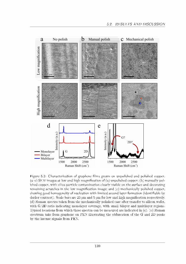
5.2. RESULTS AND DISCUSSION
Inte
nsi
ty (
a.u.)
Raman Shift (cm )-1
1500 2000 2500
G?
2D?
5 µm5 µm
25 µm25 µm
5 µm5 µm
25 µm25 µm
5 µm5 µm
25 µm25 µmLow
mag
nifi
cati
on
Hig
h m
agnifi
cati
on
Mechanical polishNo polisha Manual polishb c
Inte
nsi
ty (
a.u.)
Raman Shift (cm )-1
1500 2000 2500
MonolayerBilayerMultilayer
G 2D
d e
Figure 5.3: Characterisation of graphene �lms grown on unpolished and polished copper.(a�c) SEM images at low and high magni�cation of (a) unpolished copper; (b) manually pol-ished copper, with silica particle contamination clearly visible on the surface and decoratingremaining scratches in the low magni�cation image; and (c) mechanically polished copper,showing good homogeneity of nucleation with limited second layer formation (identi�able bydarker contrast). Scale bars are 25 μm and 5 μm for low and high magni�cation respectively.(d) Raman spectra taken from the mechanically polished case after transfer to silicon wafer,with G/2D ratio indicating monolayer coverage, with small bilayer and multilayer regions.Typical locations from which these spectra can be measured are indicated in (c). (e) Ramanspectrum take from graphene on PEN illustrating the obfuscation of the G and 2D peaksby the intense signals from PEN.
139
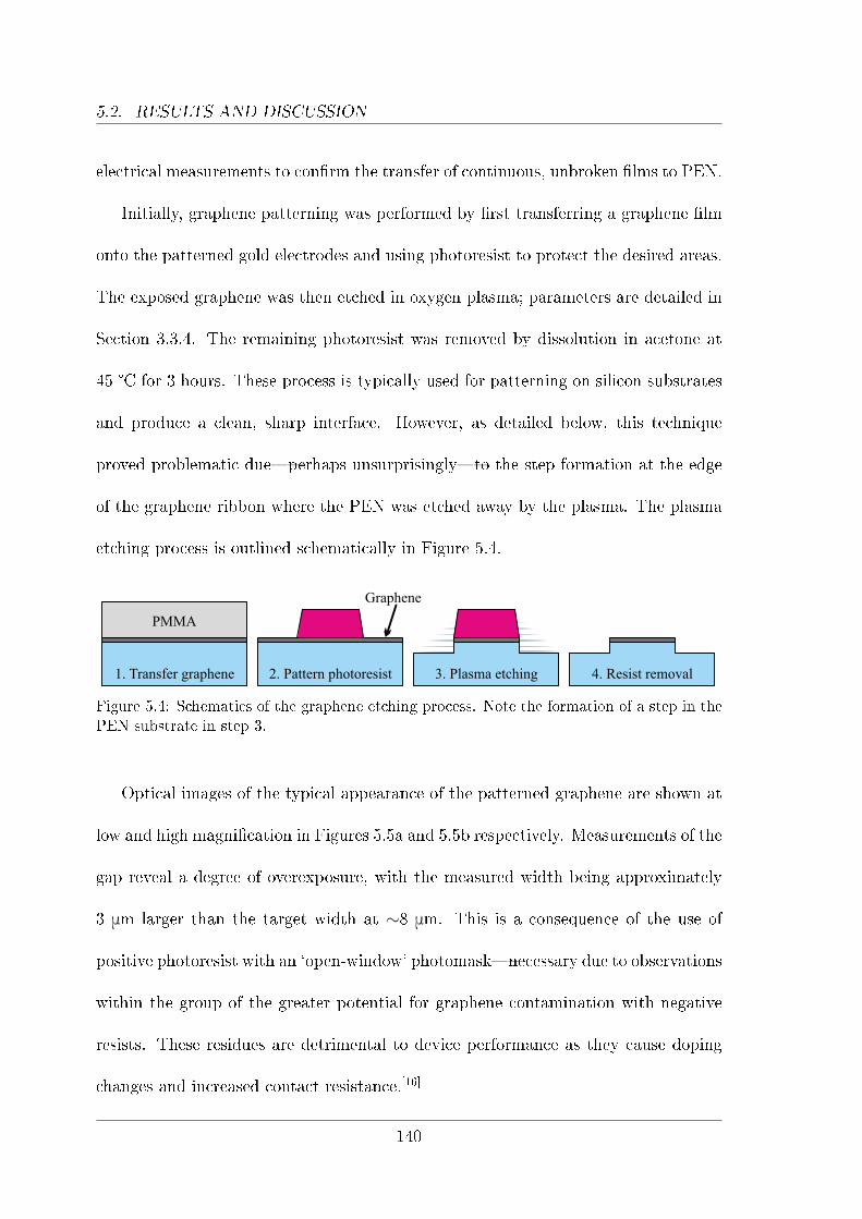
5.2. RESULTS AND DISCUSSION
electrical measurements to con�rm the transfer of continuous, unbroken �lms to PEN.
Initially, graphene patterning was performed by �rst transferring a graphene �lm
onto the patterned gold electrodes and using photoresist to protect the desired areas.
The exposed graphene was then etched in oxygen plasma; parameters are detailed in
Section 3.3.4. The remaining photoresist was removed by dissolution in acetone at
45 °C for 3 hours. These process is typically used for patterning on silicon substrates
and produce a clean, sharp interface. However, as detailed below, this technique
proved problematic due�perhaps unsurprisingly�to the step formation at the edge
of the graphene ribbon where the PEN was etched away by the plasma. The plasma
etching process is outlined schematically in Figure 5.4.
2. Pattern photoresist1. Transfer graphene 3. Plasma etching 4. Resist removal
PMMA
Graphene
Figure 5.4: Schematics of the graphene etching process. Note the formation of a step in thePEN substrate in step 3.
Optical images of the typical appearance of the patterned graphene are shown at
low and high magni�cation in Figures 5.5a and 5.5b respectively. Measurements of the
gap reveal a degree of overexposure, with the measured width being approximately
3 μm larger than the target width at ∼8 μm. This is a consequence of the use of
positive photoresist with an `open-window' photomask�necessary due to observations
within the group of the greater potential for graphene contamination with negative
resists. These residues are detrimental to device performance as they cause doping
changes and increased contact resistance.[16]
140

5.2. RESULTS AND DISCUSSION
-1 -0.5 0 0.5 1
-100
-50
0
50
100
Curr
ent
(μA
)
Voltage (V)
c d
250 µm250 µm 20 µm20 µm
0 nm
20
40
60
80
100
120
140
Trench Graphene
~70 nm~70 nm
5 µm5 µm
ba
Figure 5.5: Characterisation of graphene electrodes patterned by oxygen plasma. (a) Lowand (b) high magni�cation images detailing the junction of the gapped electrodes. Scalebars are 250 μm and 20 μm respectively. (c) AFM image of the step formed at the edge ofthe graphene electrodes during the plasma etching process (scale bar 5 μm). (d) Typicalelectrical measurement of the ungapped graphene electrodes, with standard error indicated.
The excellent contrast of the ribbon edges was the �rst indication of the deleter-
ious e�ect of the plasma on the PEN substrate; as we will observe later, due to its
high transparency, optical images of graphene typically require signi�cant contrast
enhancement. To measure the magnitude of this step, we examined the edge of the
graphene at the device channel using AFM (Figure 5.5c). This image clearly reveals
the large step height of ∼70 nm. The etching also led to a near-doubling of the surface
roughness from Rq = 6.9 ± 1 nm (as measured in Figure 4.9) to Rq = 12.1 ± 1 nm.
Nevertheless, we proceeded with the device fabrication using this method, to determ-
141

5.2. RESULTS AND DISCUSSION
ine: whether photodetection was still possible, and what e�ect the step would have on
device performance. We measured the ungapped control electrodes and found them
to be highly conductive, comparable to electrodes fabricated on silicon substrates (see
Figure 5.11c). A typical I-V curve is shown in Figure 5.5d, showing linear behaviour
over the full range of applied bias. Electrical measurements were performed by con-
tacting the source and drain electrodes and measuring the current �ow as a bias was
applied across the device. The full procedure is described in Section 3.7.1.1.
Having successfully fabricated highly conductive electrodes, we went on to meas-
ure the changes to the I-V behaviour during the application of strain. As in Chapter 4,
strain was applied in situ using a custom-built holder mounted to the sample stage.
This enabled �ne control of the radius of curvature of the substrate, and thus the
strain in the substrate surface. An image of the setup, showing a device in posi-
tion during testing, is shown in Figure 5.6a. As strain was applied, we observed a
pronounced reduction in the conductivity of the graphene ribbons, likely indicating
damage as this exceeds previous observations of increased resistance in strained CVD
graphene (Figure 5.6b).[17�19] This reduction occurs similarly and proportionally for
all electrodes measured, in spite of small variations in the initial conductivity. As
strain was relaxed, there was a very small increase in the conductivity, and a fur-
ther small increase after some time had elapsed. This gives further evidence that the
graphene is permanently damaged by the application of strain, likely through fracture
at the graphene�Au interface, although this could not be resolved in SEM images.
In spite of the substantial reduction in conductivity as a result of strain cycling,
given the apparent stabilisation once strain was relaxed we proceeded to transfer
142

5.2. RESULTS AND DISCUSSION
Co
nd
uct
ivit
y (
μS
)
1
10
100
Strain (%)
0 0.5 1.51 2 2.5
Relax
Apply
ApplyRelaxLong t.
ba
Figure 5.6: Measurement of strained devices. (a) Image of the strain holder and device in
situ, with laser spot and probes to left hand side. (b) The e�ect of strain on the conductivityof the ungapped control electrodes, detailing the large reduction as strain is applied. Notethe apparent stabilisation at strains above 1.4 %, and the slight increase as strain is relaxed,as well as a further increase to a stable value once the sample was relaxed for >24 hours.
WS2 to the gapped electrodes using the non-aqueous transfer technique described in
Section 3.3.1. This completes the photodetector, as shown in Figure 5.1. The presence
of WS2 across the channel was veri�ed by inspection with optical microscopy, and the
fact that it was monolayer was veri�ed by the strong photoluminescence (PL) signal,
as described in Chapter 4.
We pumped the device with a 532 nm laser and measured the photoconductivity
over a range of illumination powers. In the absence of strain the devices show fairly
weak photoconductivity (Figure 5.7a), signi�cantly less than those demonstrated on
silicon for the same gap width (cf. the μA order currents observed by Tan et al.,[6]
∼2 orders of magnitude larger than those observed here), with responsivity (ratio of
incident power to measured photocurrent)[20] of up to ∼5 μA/W at a bias of 6 V and
an illumination power of 0.83 kW cm-2. We believe this is likely due to a reduction in
the exciton lifetime as a result of the higher substrate roughness, the larger channel
143
5.2. RESULTS AND DISCUSSION
length and the e�ect of the step in the substrate at the graphene edge. We later fabric-
ated control devices on silicon substrates and found more comparable photocurrents
(Figure 5.12b).
Time dependent measurements reveal that the photocurrent is reasonably stable,
with modest rise and fall times (the time taken to reach 90 % of the current in the on
or o� state, respectively) of ∼2 seconds. (Figure 5.7b). At higher laser powers we did
observe some reduction of photoconductivity, presumably due to laser induced dam-
age, but with control of the laser power stable behaviour could be reached. However,
during the application of strain the devices rapidly failed, with all photoconductivity
lost by around 1 % strain (Figure 5.7c & 5.7d). This far outstrips the reduction
in conductivity observed in the graphene control electrodes, with �99 % of the ap-
plied voltage dropped over the WS2 junction even at the lowest conductivity for the
graphene, indicating an additional mechanism that is leading to device failure.
To elucidate the cause of device failure, we compared SEM images of the devices
before and after the strained photoconductivity measurements had been performed.
Prior to the measurements, the channel could be imaged free of charging due to the
conductive WS2 and graphene dissipating the build up of charge. Once the device
had been strained, we observed fracture/removal of the WS2 at the interface with the
graphene electrode that resulted in exposure of the PEN substrate, as indicated by the
obvious charging visible in this region at higher magni�cation (Figure 5.8). Though
this damage was always seen at the edge of the graphene electrode, in Figure 5.8a
it can be seen that the failure is in a monolayer region (again con�rmed by PL
measurement), while in Figure 5.8b failure occurs at the tip of a multilayer region
144

5.2. RESULTS AND DISCUSSION
-6 -4 -2 0 2 4 6-4
-2
0
2
4
6
Curr
ent
(nA
)
Voltage (V)
0.070.832.194.005.416.12
Power (kW cm )-2
Dark
0.0 0.5 1.0 1.5 2.0 2.5
0.01
0.1
1
Curr
ent
(nA
)
Strain (%)
ApplyRelaxLong t.
Relax
Apply
b
c d
-1.0
-0.5
0.0
0.5
1.0
Curr
ent
(nA
)
-6 -4 -2 0 2 4 6
Voltage (V)
00.40.7
12.50Long t.
Strain (%)
0 20 40 60 80
0.0
Cu
rren
t(n
A)
Time (s)
0.5
1.0
a
Figure 5.7: Electrical measurements of the plasma patterned photodetectors. (a) Powerdependence of a typical device, showing the small photocurrent generated and its increasewith irradiation intensity. An example of the reduction in current due to damage at higherlaser power is circled in the lower left. (b) Typical time dependent measurements of aplasma patterned device, showing the stability and modest rise and fall times of ∼2 seconds.(c,d) Strain dependence of the measured photocurrent. A constant laser power of 0.83 kWcm-2 and bias of 6 V was used unless otherwise stated.
that we commonly �nd at the centre of CVD-grown WS2. The latter case is likely
due to a concentration of current �ow into the monolayer region from the top point of
the more highly conductive multilayer triangle. Due to the observed damage from the
plasma etching process at the graphene electrode edges, it was necessary to determine
whether the resultant step and increased roughness were responsible for breaking the
WS2, likely through stress concentration at the sharp interface.
145

5.2. RESULTS AND DISCUSSION
20 µm20 µm
20 µm20 µm
5 µm5 µm
5 µm5 µm
2.5 µm2.5 µm
2.5 µm2.5 µm
20 µm20 µm
20 µm20 µm
5 µm5 µm
5 µm5 µm
2.5 µm2.5 µm
2.5 µm2.5 µm
Bef
ore
mea
sure
men
tB
efore
mea
sure
men
tA
fter
mea
sure
men
tA
fter
mea
sure
men
t
Dev
ice
1D
evic
e 2
High magnificationLow magnificationa
b
WS2
Gr
WS2
Gr
Figure 5.8: SEM images showing two devices before and after the photoconductivity meas-urement under an applied strain of 1.6 %. As indicated (red arrows), both devices showclear evidence of failure after the measurement, with device 1 (a) showing fracture acrossmonolayer regions, and device 2 (b) showing fracture concentrated around a multilayer is-land, identi�able by its triangular shape and strong contrast. Note bright charged regionsat damage sites in after images at higher magni�cation. From left to right, scale bars are:20 μm, 5 μm, and 2.5 μm.
146

5.2. RESULTS AND DISCUSSION
A di�erent patterning approach was required for producing graphene electrodes
without damaging the PEN substrate. Recently, Trung et al.[21] demonstrated a
process analogous to the gold lift-o� process used here (described in Section 3.3.3).
Here the photoresist is used not to protect selected areas of the graphene from removal,
but to mask o� areas such that a transferred layer of graphene may only contact the
substrate in the desired pattern. A substantially thinner PMMA sca�old was used to
facilitate improved conformation of the transferred graphene �lm with the patterned
photoresist. We tested a 50 nm �lm (as was used to modify the surface of the PEN
substrate in Chapter 4), but found that this was too fragile to transfer and resulted
in fragmentation of the �lm; a 100 nm �lm was found to give acceptable results. The
samples were dried overnight, hardbaked to ensure proper contact of the graphene
with the PEN surface, and the photoresist and transfer sca�old removed in acetone.
The excess graphene not in contact with the substrate was scissioned using a brief
ultrasonic treatment and washed away, leaving the desired pattern on the substrate. A
schematic detailing the process is shown in Figure 5.9, and the speci�cs are described
in Section 3.3.4.2.
1. Pattern photoresist 2. Transfer graphene 3. Hard bake 4. Ultrasonic lift-off
Figure 5.9: Schematic detailing the graphene lift-o� process. A layer of graphene with100 nm PMMA sca�old is transferred onto the patterned resist (1 μm S1813), left to dry,and baked to ensure conformation to the pattern. The excess graphene is removed byultrasonication and washing with IPA.
Next, we focussed on optimising the photolithography process to achieve stable
147

5.2. RESULTS AND DISCUSSION
and consistent patterning with the minimum possible gap width. The 45 mJ cm-2
dose used for the gold patterning was found to be too high to reproduce the 5 μm gap
on the mask, resulting in removal of this region due to overexposure. By reducing
the dose to 25 mJ cm-2, we were able to preserve this feature while still producing
clean surfaces after development. As the resist pro�le can be strongly a�ected during
development, we also tested the development time by parametrising the patterned
ribbon quality in terms of gap width before and after graphene patterning, and the
yield of successful patterning. These results are summarised in Figure 5.10a. Shorter
times led to underdevelopment, resulting in an apparent gap width several microns
larger than the desired gap before patterning due to residual resist at the pattern
edges, and a �nal ribbon width at least 1 μm larger. Increasing the development time
up to 70 seconds gave a reduction down to 5�6 μm, which was considered acceptable
for our purposes. For all development times, the yield remained above >90 %.
Example images of the patterned ribbons are shown at low and high magni�cation
in Figures 5.10b and 5.10c respectively. Note the reasonably sharp ribbon edges and
lack of visible damage, representing a fourfold improvement in patterning resolution
when compared to the work of Trung et al.[21] Ultrasonication time also plays an
important role in the �nal ribbon quality, with 30 seconds found to be adequate.
Shorter times result in residual graphene at the ribbon edges, a typical example of
which is shown in Figure 5.10d, imaged identically to the well de�ned ribbon shown in
Figure 5.10c. We also demonstrated this patterning on silicon wafers, with comparable
results obtained using the same parameters, though a much shorter ultrasonication
time of 5 seconds was su�cient to scission the excess graphene, and in fact still
148

5.2. RESULTS AND DISCUSSION
SEM of silicon device
20 µm20 µm
ee
250 µm250 µm 20 µm20 µm
SEM of silicon device
20 µm20 µm
50 60 700
2
4
6
8
10
Spac
ing (
µm
)
Development Time (s)
0
20
40
60
80
100
Yie
ld (
%)
Before lift-off After lift-offChange Yield
c
d
b c
d
a
b
Figure 5.10: Characterisation of the graphene electrodes patterned by lift-o�. (a) Changesto the measured gap width before and after lift-o� with increasing development time, and theyield of successfully patterned junctions. (b) Low magni�cation (scale bar 250 μm) opticalimage of successfully patterned ribbons on PEN. (c�e) High magni�cation (scale bar 20 μm)optical images of: (c) successfully patterned gap and (d) unsuccessfully patterned gap, dueto insu�cient sonication; and (e) SEM image of a gap patterned by lift-o� on silicon wafer.Note wider gap and presence of cracking visible in (e) due to more e�cient transmission ofvibration through silicon than PEN.
149
5.2. RESULTS AND DISCUSSION
resulted in cracking to the graphene edges and a noticeably larger gap width of ∼8 μm
(Figure 5.10e).
The graphene control electrodes were once again characterised by I-V measure-
ment. Before the application of strain, they show near identical conductivity to
the plasma-patterned electrodes demonstrated above, indicating that patterning by
lift-o� produces ribbons of equivalent quality to plasma patterning, without the as-
sociated damage to the PEN substrate. When strain was applied, we once again
found that the graphene ribbons experience a signi�cant reduction in conductivity,
con�rming that this e�ect is independent of the graphene patterning technique used
(Figure 5.11a). We tested the e�ect of a mild vacuum annealing process (120 °C at
6 μbar for 8 hours) to see if this could be used to improve the conductivity of the
ribbons, but this was found to instead be slightly detrimental (Figure 5.11b). We
also tested if this technique might be used to restore the conductivity after straining
but observed no signi�cant change.
With the quality of the graphene electrodes con�rmed, we again proceeded to fab-
ricate photodetectors by transferring domains of WS2 to the gapped electrodes, and
performed measurements as before. Unstrained behaviour was similar, with weak
but measurable photoconductivity that increased with laser power (Figure 5.12a).
As mentioned above, control devices fabricated on silicon using the same technique
showed photocurrent 1�2 orders of magnitude greater than the PEN devices (Fig-
ure 5.12b). Time dependent measurements reveal an improvement to the rise and
fall times, typically found to be less than the measurement interval of 80 ms (Fig-
ure 5.12c). We then performed the strain dependent measurements. Once again, the
150

5.2. RESULTS AND DISCUSSION
-100
-50
0
50
100
0-0.5-1 0.5 1Voltage (V)
Curr
ent
(μA
)
BeforeAfter
Annealing
b
c
0.0 0.5 1.0 1.5 2.0 2.5
10
100
Conduct
ance
(μS
)
Strain (%)
Relax
Apply
ApplyRelaxLong t.
a
-100
-50
0
50
100
0-0.5-1 0.5 1
Voltage (V)
Curr
ent
(μA
)
PEN Plasma
Si Lift-offPEN Lift-off
Figure 5.11: Changes to the conductivity of ungapped lift-o� patterned graphene electrodes.(a) Large reduction as a result of strain cycling and (b) small reduction as a result of vacuumannealing. (c) Comparison of lift-o� patterning on silicon wafer and PEN substrate, withplasma-patterned graphene replotted for reference.
devices failed (Figure 5.12d & 5.12e). However, in this case we measured a transient
increase of up to one order of magnitude as shown in Figure 5.12d, the mechanism
for which we propose below.
To ascertain if the devices were failing by the same mechanism as the graphene
electrodes, where the conductivity reduced to a stable value for a given applied strain,
we performed a small strain cycle several times to the devices and repeated the
measurements again. In contrast to the ungapped electrodes, the behaviour was not
stable with successive cycles, with complete loss of photoconductivity in all devices
151

5.2. RESULTS AND DISCUSSION
following the second cycle (Figure 5.12f). This suggests that failure occurs by strain-
and-laser-mediated electrical damage.
0.0 0.5 1.0 1.5 2.0 2.5
0.01
0.1
1
Curr
ent
(nA
)
Strain (%)
ApplyRelaxLong time
Relax
Apply
-2
-1
0
1
2
Curr
ent
(nA
)
-6 -4 -2 0 2 4 6
Voltage (V)
00.40.7
12.50Long time
Strain (%)
-100
-50
0
50
100
Curr
ent
(nA
)-6 -4 -2 0 2 4 6
Voltage (V)
0.83
2.19
4.00
5.41
6.12
Power (kW cm )-2
Dark
0 20 40 60
0
0.5
1
Curr
ent
(nA
)
Time (s)
b
c d
-6
-4
-2
0
2
4
6
-6 -4 -2 0 2 4 6
Voltage (V)
Curr
ent
(nA
)
0.070.832.194.005.416.12
Power (kW cm )-2
Dark
a
e f
Curr
ent
(nA
)
Strain (%)
0.0 0.2 0.4 0.6
0
1
2
3
4
1st Cycle2nd Cycle
PEN Silicon
Figure 5.12: Photodetection of the lift-o� patterned devices. Laser power dependence of themeasured photocurrent for devices on (a) PEN and (b) silicon substrates, showing 1�2 ordersof magnitude enhancement for silicon over PEN. (c) Typical time dependence for device onPEN, showing rapid switching. (d) Example I-V curves showing the largest transient increaseof photocurrent observed, and (e) average response of the devices to strain cycling. (f) Smallstrain cycling of devices showing that the mechanism contributing to failure is cumulative.A constant laser power of 0.83 kW cm-2 and bias of 6 V was used unless otherwise stated.
152

5.2. RESULTS AND DISCUSSION
Band structures for the photodetector are shown in Figure 5.13. In the unbiased
case (Figure 5.13a), no current is observed as there is no �eld to separate the strongly
bound excitons nor overcome the potential barriers at either interface. In contrast,
a single Schottky barrier produces current at zero bias due to separation of excitons
in the depletion region. Applying a small bias without strain (Figure 5.13b) leads
to limited current �ow, however the majority of electrons remain `trapped' in the
potential well between the two Schottky barriers. Applying a larger bias reduces the
height of the forward biased barrier, eventually leading to the �at-band condition
as shown in Figure 5.13c and enhanced photocurrent due to ready separation of
excitons.[22]
Φbn
EF
Φbp
hν
Gr GrWS2
e-
h+
Gr GrWS2
VBhν
Gr GrWS2
VB
hν
Iph
Gr GrWS2
VB
Iph
hν
a b
c d
Figure 5.13: Idealised band structures for the photodetectors, showing the back to backSchottky barriers typical for MSM photodetectors. (a) Equilibrium diagram showing aphotogenerated exciton trapped in a potential well, with no photocurrent (Iph) generated.(b�d) Non equilibrium diagrams at (b) small bias with potential well still present and (c)large bias in the �at-band condition. (d) The application of strain lowers the magnitude ofthe bias necessary for the �at-band condition.
153
5.2. RESULTS AND DISCUSSION
We propose that at small strains and prior to device failure, the transient en-
hancement of photocurrent occurs by a reduction in the bias required to achieve the
�at-band condition (Figure 5.13d) due to the reduced bandgap and the piezotronic
e�ect (where the Schottky barrier height is reduced by polarisation charges in strained
TMDs).[23] Here we also illustrate a further possible mechanism for photocurrent gen-
eration: photoexcitation of carriers over the barrier from graphene to WS2, similarly
enhanced by the reduction of the bandgap.[24] Further increases may be ascribed to
similar reasons as the strain-induced increase in PL intensity described in Chapter 4�
an increase in the absorbance cross-section and reduction in the drain of carriers from
the K to the∑
conduction band minima limiting recombination.
In an e�ort to isolate the cause of failure, we separately measured devices that
had been: strained (Figure 5.14a); strained and biased (Figure 5.14b); strained and
irradiated (Figure 5.14c); and strained, biased, and irradiated (Figure 5.14d). Prior
SEM measurements demonstrate that the WS2 was intact across at least part of the
junction in all cases. We then measured the devices and veri�ed stable photocon-
ductance prior to the application of strain. Despite the absence of obvious damage,
with no observable di�erence between the before and after images in Figure 5.14, in
all cases the devices were con�rmed as having failed after the application of 1.2 %
strain, regardless of bias or irradiation.
Given the resolution limitations of SEM images as a result of the insulating PEN
substrate, one explanation for failure could be the formation of cracks of a size below
these limits. AFM was not attempted due to the high substrate roughness preventing
imaging of 2D materials (as described in Chapter 4). In the plasma etched case, the
154

5.2. RESULTS AND DISCUSSION
20 µm20 µm
20 µm20 µm 5 µm5 µm
20 µm20 µm5 µm5 µm20 µm20 µm
20 µm20 µm 5 µm5 µm 20 µm20 µm
5 µm5 µm
20 µm20 µm
20 µm20 µm
Bef
ore
mea
sure
men
tB
efore
mea
sure
men
tA
fter
mea
sure
men
tA
fter
mea
sure
men
t
Device 1 - strained Device 2 - strained & biased
High magnificationLow magnification
a
c
5 µm5 µm
5 µm5 µm
5 µm5 µm
5 µm5 µm
High magnificationLow magnification
Device 3 - strained & irradiated Device 4 - strained, biased & irradiated
b
d
WS2WS2Gr
Figure 5.14: SEM images of the lift-o� patterned devices, immediately after WS2 had beentransferred and following the measurement. We applied (a) strain; (b) strain and bias; (c)strain and laser irradiation; and (d) strain, bias, and laser irradiation. The dashed linesindicate the approximate position of the graphene electrodes. Scale bars are 20 μm and5 μm for low and high magni�cation respectively.
step at the electrode edge will introduce tension to the WS2, likely expanding these
cracks to dimensions that are more easily imaged. Further experimentation is required
to verify this, either using substrates that permit higher resolution in one or both of
155

5.2. RESULTS AND DISCUSSION
these techniques, or using more advanced imaging techniques such as KPM that may
permit higher resolution. It is also possible that the debonding e�ect described in
Chapter 4 results in the loss of su�cient contact between the WS2 and graphene for
measurable current to �ow.
156

5.3. CONCLUSIONS
5.3 Conclusions
In this chapter, we explored conventional and new fabrication techniques for the pro-
duction of all-2D lateral photodetectors on �exible substrates. During the course of
studying what impact the use of soft matter substrates had on their e�cacy, sev-
eral issues with the conventional techniques were identi�ed. We �rst modi�ed the
gold contact patterning process to remove the need for an adhesion layer, then used
the typical oxygen plasma etching process to pattern graphene and produce working
devices that showed measurable photoconductivity, but found that the devices failed
rapidly upon the application of small tensile strains.
Analysis of the devices before and after the application of strain and consequent
failure revealed a stable reduction of the conductivity of the graphene electrodes, pre-
sumably due to damage at the graphene�gold interface sustained during straining,
but this was not su�cient to explain the complete loss of photoconductivity. More
importantly, signi�cant damage to the WS2 was observed at the edge of the graphene
electrodes following the strained photoconductance measurements�suspected to be
a consequence of damage to the substrate surface sustained during the plasma etch-
ing of graphene. In response to this, we developed a modi�ed lift-o� process that
enabled high quality patterning of graphene without damaging the PEN substrate
surface and re�ned this process to produce features down to <10 μm resolution, an
improvement over previous demonstrations of this technique. We proceeded to fab-
ricate photodetector devices using this method. Despite minor improvements and an
initial transient enhancement of the measured photocurrent by up to one order of
157

5.4. ACKNOWLEDGEMENTS
magnitude, we found that the devices still failed in response to small tensile strains.
Due to resolution limits imposed on both SEM and AFM by the polymer sub-
strates, we were unable to directly determine the cause of failure of the lift-o� pat-
terned devices. In contrast to the damage to the devices that were patterned with
plasma, which could be imaged by SEM due to built in tension opening the fracture
interface su�ciently for it to be imaged, we propose that failure occurs by damage at
the interface between the graphene and WS2 of a scale below these resolution limits.
5.4 Acknowledgements
AFMmapping of the graphene electrodes was performed by Mr Xiaochen Wang. As in
Chapter 4, the majority of the 2D materials used here were grown by the author, but
some materials were provided by: Dr Yuewen Sheng (WS2 and unpolished graphene
that was used in early device tests), and Miss Linlin Hou (WS2). Photomasks were
generously provided by Dr Chit Siong Lau. Dr Jason Brown was of great help during
the photolithographic fabrication process, and Dr Haijie Tan contributed to the device
design and fabrication processes.
158

Bibliography
[1] F. H. L. Koppens, T. Mueller, P. Avouris, A. C. Ferrari, M. S. Vitiello, M.Polini, �Photodetectors Based on Graphene, Other Two-Dimensional Materialsand Hybrid Systems�, Nature Nanotechnology 2014, 9, 780�793.
[2] A. Bablich, S. Kataria, M. Lemme, �Graphene and Two-Dimensional Materialsfor Optoelectronic Applications�, Electronics 2016, 5, 13.
[3] Y. Fan, Y. Zhou, X. Wang, H. Tan, Y. Rong, J. H. Warner, �PhotoinducedSchottky Barrier Lowering in 2D Monolayer WS2 Photodetectors�, AdvancedOptical Materials 2016, 4, 1573�1581.
[4] S. Kallatt, G. Umesh, N. Bhat, K. Majumdar, �Photoresponse of AtomicallyThin MoS2 Layers and Their Planar Heterojunctions�, Nanoscale 2016, 8,15213�15222.
[5] M. W. Iqbal, M. Z. Iqbal, M. F. Khan, M. A. Kamran, A. Majid, T. Alharbi,J. Eom, �Tailoring the Electrical and Photo-Electrical Properties of a WS2Field E�ect Transistor by Selective n-Type Chemical Doping�, RSC Advances2016, 6, 24675�24682.
[6] H. Tan, Y. Fan, Y. Zhou, Q. Chen, W. Xu, J. H. Warner, �Ultrathin 2D Pho-todetectors Utilizing Chemical Vapor Deposition Grown WS2 with GrapheneElectrodes�, ACS Nano 2016, 10, 7866�7873.
[7] H. Tan, W. Xu, Y. Sheng, C. S. Lau, Y. Fan, Q. Chen, M. Tweedie, X.Wang, Y. Zhou, J. H. Warner, �Lateral Graphene-Contacted Vertically StackedWS2/MoS2 Hybrid Photodetectors with Large Gain�,Advanced Materials 2017,29, 1702917.
[8] J. Vancea, G. Reiss, F. Schneider, K. Bauer, H. Ho�man, �Substrate E�ectson the Surface Topography of Evaporated Gold Films: A Scanning TunnellingMicroscopy Investigation�, Surf. Sci. 1989, 218, 108�126.
[9] R. Compton, C. Bamford, C. Tipper, Ester Formation and Hydrolysis andRelated Reactions, Elsevier Science, 1972.
[10] M. J. Cordill, A. Taylor, J. Schalko, G. Dehm, �Fracture and Delamination ofChromium Thin Films on Polymer Substrates�,Metall. Mater. Trans. A 2010,41, 870�875.
159
[11] P. Braeuninger-Weimer, B. Brennan, A. J. Pollard, S. Hofmann, �Understand-ing and Controlling Cu-Catalyzed Graphene Nucleation: The Role of Impur-ities, Roughness, and Oxygen Scavenging�, Chemistry of Materials 2016, 28,8905�8915.
[12] P. S. Sidhu, R. J. Gilkes, R. M. Cornell, A. M. Posner, J. P. Quirk, �Dissolutionof Iron Oxides and Oxyhydroxides in Hydrochloric and Perchloric Acids�, Claysand Clay Minerals 1981, 29, 269�276.
[13] F. Bondioli, A. M. Ferrari, C. Leonelli, T. Manfredini, �Syntheses of Fe2O3/SilicaRed Inorganic Inclusion Pigments for Ceramic Applications�, Materials Re-search Bulletin 1998, 33, 723�729.
[14] H. Shinohara, Y. Yamakita, K. Ohno, �Raman Spectra of Polycyclic Aro-matic Hydrocarbons: Comparison of Calculated Raman Intensity Distributionswith Observed Spectra for Naphthalene, Anthracene, Pyrene, and Perylene�,Journal of Molecular Structure 1998, 442, 221�234.
[15] E. J. Heller, Y. Yang, L. Kocia, W. Chen, S. Fang, M. Borunda, E. Kaxiras,�Theory of Graphene Raman Scattering�, ACS Nano 2016, 10, 2803�2818.
[16] B. B. Kantar, M. Özturk, H. Çetin, �The E�ects of Lithographic Residues andHumidity on Graphene Field E�ect Devices�, Bulletin of Materials Science2017, 40, 239�245.
[17] K. S. Kim, Y. Zhao, H. Jang, S. Y. Lee, J. M. Kim, K. S. Kim, J.-H. Ahn,P. Kim, J.-Y. Choi, B. H. Hong, �Large-Scale Pattern Growth of GrapheneFilms for Stretchable Transparent Electrodes�, Nature 2009, 457, 706�710.
[18] Y. Lee, S. Bae, H. Jang, S. Jang, S.-E. Zhu, S. H. Sim, Y. I. Song, B. H.Hong, J.-H. Ahn, �Wafer-Scale Synthesis and Transfer of Graphene Films�,Nano Lett. 2010, 10, 490�493.
[19] X. W. Fu, Z. M. Liao, J. X. Zhou, Y. B. Zhou, H. C. Wu, R. Zhang, G. Jing, J.Xu, X. Wu, W. Guo, D. Yu, �Strain Dependent Resistance in Chemical VaporDeposition Grown Graphene�, Appl. Phys. Lett. 2011, 99, 2013�2016.
[20] J. P. Dakin, R. G. W. Brown, Handbook of Optoelectronics, Vol. 1, CRC Press,2010, pp. 73�80.
[21] T. N. Trung, D.-O. Kim, J.-H. Lee, V.-D. Dao, H.-S. Choi, E.-T. Kim, �Simpleand Reliable Lift-O� Patterning Approach for Graphene and Graphene-AgNanowire Hybrid Films�, ACS Applied Materials & Interfaces 2017, 9, 21406�21412.
[22] F. Omnes, D. Decoster, H. Joseph,Optoelectronic Sensors, Vol. 1, Wiley, 2010,pp. 1�14.
[23] J. Guo, R. Wen, Y. Liu, K. Zhang, J. Kou, J. Zhai, Z. L. Wang, �PiezotronicE�ect Enhanced Flexible Humidity Sensing of Monolayer MoS2�, ACS AppliedMaterials & Interfaces 2018, 10, 8110�8116.
[24] F. A. Padovani, R. Stratton, �Field and Thermionic-Field Emission in SchottkyBarriers�, Solid State Electronics 1966, 9, 695�707.
160

Chapter 6
Piezoelectric Sensors with Graphene
Electrodes for Pre-Clinical
Cardio-Respiratory Monitoring
6.1 Introduction
As outlined in Section 2.3.3.8, there are a number of drawbacks with the existing
cardiac and respiratory monitoring technology used in small animal MRI and CT
imaging. These devices are used to monitor the key sources of body motion during
imaging, enabling correction and stabilisation of the image in a process known as gat-
ing. This leads to improved image resolution, and is necessary to avoid artefacts that
can lead to misdiagnosis.[1,2] Current respiratory monitoring technology (pneumatic
capsules known as respiratory balloons, Figure 6.1a & 6.1d) is not favoured due to
complicated setup, sensitivity to changes in air pressure, and the need to recalibrate
161

6.1. INTRODUCTION
if the animal is moved between di�erent pieces of equipment. Silver-contacted piezo-
electric sensors (Figure 6.1b & 6.1e) have been demonstrated to be e�ective at solving
these issues but are almost universally avoided due to the use of metal components,
which lead to signi�cant artefacts in both imaging techniques.[3�7]
In this chapter, we demonstrate that large area, CVD grown monolayer graphene
�lms are the ideal electrode material for replacing metallic conductors in piezoelectric
respiratory monitors. Graphene inks were also trialled, but signi�cant reductions in
the measured respiratory signal from early prototypes during MRI scanning precluded
further study. We explore the necessary modi�cations to the existing fabrication
processes, and characterise the graphene �lms to demonstrate the high quality of
graphene before and after transfer. The fabricated devices (Figure 6.1c) are studied
in a range of di�erent mounting con�gurations to determine the optimal mounting
conditions, and assessed for their fatigue resistance. We further go on to demonstrate
their use for respiratory gating in vivo as part of an all carbon based monitoring and
life support cradle, showing that high quality images can be obtained without metal
induced artefacts, and with facile device mounting and setup.
In marked contrast to the complicated setup and observation of signi�cant arte-
facts when using respiratory balloons or metal contacted piezoelectric devices, respect-
ively, our device was easily and rapidly implemented in both imaging techniques, was
highly radiolucent, and was found to cause little distortion to the magnetic �eld of
the MRI scanner. We further demonstrate that due to the high sensitivity of the
sensor it is possible to measure the animal's cardiac cycle, o�ering the possibility of
combining both cardiac and respiratory gating facilities into a single unit.
162

6.2. RESULTS AND DISCUSSION
eV
d
a b c
Polymer balloon
PiezoelectricpolymerAg or Graphene
Respiratory balloon: Piezoelectric transducer:
Air
Force Force
Figure 6.1: Images and schematics of the existing technology and our sensor. (a�c) Images ofthe (a) respiratory balloon,[8] (b) silver-contacted sensor, and (c) graphene-contacted sensor.(d,e) Diagrams of the (d) respiratory balloon and (e) piezoelectric transducer. The designin (e) is shared by the existing silver-contacted sensor and our graphene-contacted sensor.
6.2 Results and Discussion
We again grew �lms of graphene by our previously reported methods (detailed in
Section 3.2.1). SEM images of the as grown graphene �lms are shown in Figure 6.2a
& 6.2b. Large area �lms up to 70 × 120 mm were spin coated with PMMA, and
etched and washed as before. In this case we etched the copper foil in large trays, and
exchanged the etchant using large volume syringes to minimise disturbance to the �lm.
The etchant also had to be refreshed once during etching to ensure complete removal
of the copper. We used 110 μm thick, uniaxially oriented �lms of the piezoelectric
polymer poly(vinylidene �uoride) (PVDF; Precision Acoustics) as a substrate, chosen
for its large piezoelectric coe�cient (d33 = -30 pC/N).[9] This relatively thick �lm
was chosen for its balance of durability and strength, �exibility, and magnitude of
163

6.2. RESULTS AND DISCUSSION
generated voltage. The voltage generated may be increased by using a thicker �lm,
at the cost of increased sti�ness and decreased internal capacitance�leading to more
rapid signal decay and, as we will see later, an increase in the cut-o� frequency below
which signals are attenuated.[10]
Transfer was complicated by the requirement that graphene be transferred onto
both sides of the �lm. This issue was compounded by the low working temperature
of PVDF (75 °C), which precluded the baking steps usually used before transfer to
remove any solvent residues, and after transfer to promote adhesion, as higher tem-
peratures will degrade device performance by causing misorientation of the polymer
chains.[9,10]
In lieu of baking, we opted instead to drive o� solvent residues by placing the
cleaned PVDF in a vacuum desiccator for 30 minutes. Adhesion was promoted after
transfer by simply extending the drying time, and the redeposition of a thin layer of
PMMA to aid conformation of the graphene to the substrate surface. Previous work
has demonstrated that this is e�ective at improving the quality and reducing the res-
istance of transferred graphene �lms.[11,12] SEM images of graphene �lms transferred
by aqueous methods are shown in Figure 6.2c & 6.2d. Note the similar appearance at
low magni�cation and general continuity of the �lms, though we were able to image
small cracks and damage over the surface�observed as brighter regions in the images
due to substrate charging, as well as a reproduction of the surface texture of the
PVDF. We again turned to Raman spectroscopy to verify the presence of graphene
post transfer. Raman spectra of the graphene transferred to silicon are reprinted for
comparison from the previous chapter in Figure 6.2e, and spectra from PVDF samples
164
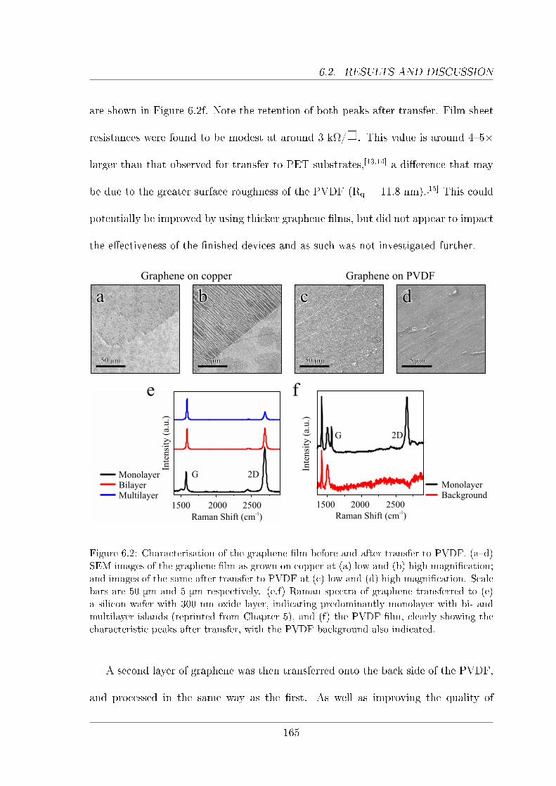
6.2. RESULTS AND DISCUSSION
are shown in Figure 6.2f. Note the retention of both peaks after transfer. Film sheet
resistances were found to be modest at around 3 kΩ/0. This value is around 4�5×
larger than that observed for transfer to PET substrates,[13,14] a di�erence that may
be due to the greater surface roughness of the PVDF (Rq = 11.8 nm).[15] This could
potentially be improved by using thicker graphene �lms, but did not appear to impact
the e�ectiveness of the �nished devices and as such was not investigated further.
Inte
nsi
ty (
a.u.)
Raman Shift (cm )-1
1500 2000 2500
MonolayerBilayerMultilayer
G 2D
e f
MonolayerBackground
G 2D
Inte
nsi
ty (
a.u.)
Raman Shift (cm )-1
1500 2000 2500
50 µm50 µm 5 µm5 µm 50 µm50 µm 5 µm5 µm
aa bb cc dd
Graphene on copper Graphene on PVDF
Figure 6.2: Characterisation of the graphene �lm before and after transfer to PVDF. (a�d)SEM images of the graphene �lm as grown on copper at (a) low and (b) high magni�cation;and images of the same after transfer to PVDF at (c) low and (d) high magni�cation. Scalebars are 50 μm and 5 μm respectively. (e,f) Raman spectra of graphene transferred to (e)a silicon wafer with 300 nm oxide layer, indicating predominantly monolayer with bi- andmultilayer islands (reprinted from Chapter 5), and (f) the PVDF �lm, clearly showing thecharacteristic peaks after transfer, with the PVDF background also indicated.
A second layer of graphene was then transferred onto the back side of the PVDF,
and processed in the same way as the �rst. As well as improving the quality of
165
6.2. RESULTS AND DISCUSSION
the transferred �lm, the redeposition of PMMA has the additional bene�t of sealing
the edges, thereby preventing delamination of the �rst layer during transfer of the
second. The protected �lm was subsequently diced into strips of appropriate dimen-
sions, discarding the edges due to poor graphene adhesion visible here. The PMMA
was removed in acetone as before, but performed at room temperature for 48 hours
to again minimise the possibility of degrading the piezoelectricity of the PVDF. We
initially trialled thermal evaporation of gold as a method of forming the electrodes
before transfer, but found that even at deposition rates <0.1 nm s-1, there was suf-
�cient �ux of heat into the PVDF to cause signi�cant warping. We instead formed
electrodes using silver paint (RS Components) encapsulated in epoxy (Araldite®).
The device was completed by laminating the entire assembly in polypropylene (PP)
tape bonded with pressure sensitive adhesive, protecting the exposed graphene from
damage. This process is outlined schematically in Figure 6.3.
We �rst fabricated small scale prototype devices (10 × 50 mm) using the above
methods, to test the e�cacy of graphene in this application. Facile mounting of the
device�by simply placing it in contact with the body when it was loaded into the
cradle�led to very e�ective monitoring of the respiratory cycle and, to our surprise,
we were additionally able to measure clear signals from the cardiac cycle. Data
from this early prototype device, as well as from a respiratory balloon monitoring
the same subject, are plotted in Figure 6.4a. Note the faster rise and fall times
produced by our sensor, as well as the presence of cardiac signals that are absent in
the respiratory balloon trace. We also plot an example of the trigger produced from
the peak of the respiratory signal that is subsequently converted into a gating signal�
166

6.2. RESULTS AND DISCUSSION
PVDF PMMA PP Tape
a b
c d
Figure 6.3: Schematics detailing the fabrication of the graphene contacted respiratory mon-itor. (a) A layer of graphene is transferred to one side of the PVDF. (b) After drying, asecond layer of PMMA is deposited on the transferred �lm to prevent detachment duringtransfer of a second graphene layer to the other side. (c) The �lm is cut into strips of therequisite dimensions, and the PMMA removed. (d) Contacts are fabricated and the deviceis encapsulated in polypropylene (PP) tape.
where acquisition is turned on during the peaks and o� during the troughs, when the
body is in motion. We went on to perform basic scans to prove the functionality
of the device. In the ungated image (Figure 6.4b), respiration causes distortion of
the image, most prominently causing the liver to periodically move out of frame.
With gating, the image is stable (Figure 6.4c). Figure 6.4d shows a CT image of
the mouse with the region where the most disturbance occurs around the liver and
lungs highlighted. Having veri�ed the working principle and MRI compatibility, we
167
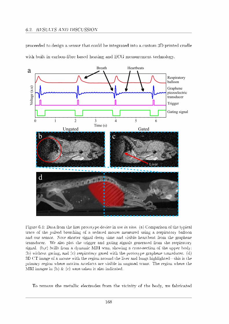
6.2. RESULTS AND DISCUSSION
proceeded to design a sensor that could be integrated into a custom 3D printed cradle
with built in carbon-�bre based heating and ECG measurement technology.
Respiratoryballoon
Graphenepiezoelectrictransducer
a
cb
Liver
Ungated Gated
0 1 2 3 4 5 6
Time (s)
Volt
age
(a.u
)
Trigger
Gating signal
Breath Heartbeats
d
Figure 6.4: Data from the �rst prototype device in use in vivo. (a) Comparison of the typicaltrace of the pulsed breathing of a sedated mouse measured using a respiratory balloonand our sensor. Note shorter signal decay time and visible heartbeat from the graphenetransducer. We also plot the trigger and gating signals generated from the respiratorysignal. (b,c) Stills from a dynamic MRI scan, showing a cross-section of the upper body:(b) without gating, and (c) respiratory gated with the prototype graphene transducer. (d)3D CT image of a mouse with the region around the liver and lungs highlighted�this is theprimary region where motion artefacts are visible in ungated scans. The region where theMRI images in (b) & (c) were taken is also indicated.
To remove the metallic electrodes from the vicinity of the body, we fabricated
168

6.2. RESULTS AND DISCUSSION
larger sensors (12 × 120 mm). In an e�ort to quantify their behaviour and determine
the optimal mounting geometry, we simulated the respiratory signal by using a custom
built actuator, equipped with a small cantilever arm mounted to a DC motor and
controlled by a timing circuit (RS Components), to apply force to the sensor. The
resultant signals were measured using a Biopac MP150 unit with DA100C ampli�er,
as detailed in Section 3.7.2, but �rst required conditioning as they were found to
exceed the limits of the detector. We reduced the signal magnitude by means of a
resistive voltage divider of appropriate transfer function (the ratio of output to input
voltage, Hdiv; Equation 6.1), in which the input signal is applied across a pair of
resistors (R1 and R2) and the output taken across the second.
Piezoelectric Transducer Potential Divider
Rp
Cp
R1
R2
Vin
Vout
Figure 6.5: Equivalent circuit diagram for piezoelectric sensor connected to voltage divider.Adapted from Karki.[16]
Hdiv =R2
R1 +R2
(6.1)
Calibration of the potential divider was necessary due to the low frequency tran-
sient signal generated by the sensor causing deviation from Equation 6.1. This can
be understood with reference to the equivalent circuit shown in Figure 6.5: the trans-
ducer itself contains a series resistance and capacitance which forms another poten-
169
6.2. RESULTS AND DISCUSSION
tial divider in the form of a passive high pass �lter, the e�ect of which varies with
frequency.[10,16] Since a more detailed analysis of the electronic properties was bey-
ond the scope of this study, rather than attempt to measure these and calculate H
directly we chose instead to estimate it by applying a very small mechanical signal,
and comparing the amplitude of divided and undivided (i.e. R1 = 0 and R2 = ∞)
signals. We achieved su�cient signal reduction with R1 = 39 kΩ and R2 = 12 kΩ,
leading to H div = 0.147 ± 0.003 (cf. H div = 0.235 given by Equation 6.1).
The high level of ampli�cation resulted in signi�cant detection of 50 Hz mains
hum, so the entire divider assembly was shielded using BNC cables and an aluminium
enclosure, and a twisted pair lead used to connect the sensor to the divider. We further
retrospectively subtracted a �tted 50 Hz sine function from the measured potential.
This was found to better preserve the signal amplitude, in contrast to low pass or
Butterworth notch �ltering, both of which led to signi�cant signal attenuation.
The sensor was mounted in a range of con�gurations and force applied along
its length, to both the negative and positive sides of the PVDF (as de�ned by the
manufacturer). The maximum applied force as given by the stall torque of the motor
at 6 V was 193 mN, and the maximum de�ection of the cantilever arm in the absence
of physical resistance was 5 mm. An image of the measurement setup is shown in
Figure 6.6a: a mechanical signal (1) stimulates the sensor (2), which is �xed to two
linear translation stages (3), producing a signal that is reduced by the potential divider
(4) before being ampli�ed (5) and measured (6), a read out of which is recorded and
displayed on a connected PC (7). The measured potentials and illustrations of the
various mounting geometries are displayed in Figure 6.6b�6.6f.
170

6.2. RESULTS AND DISCUSSION
0
10
20
30
40
0 2 4 6 8 10Position (cm)
Pote
nti
al (
mV
)
Rest
Sensor clamped
0
10
20
30
0 2 4 6 8 10Position (cm)
Pote
nti
al (
mV
)
Rib
0
5
10
15
0 2 4 6 8 10Position (cm)
Pote
nti
al (
mV
)
0
10
20
30
40
50
60
Pote
nti
al (
mV
)
0 2 4 6 8 10Position (cm)
Force
Sensor
Clamp
1
23
4
5
6
1
23
4
5
677
33
0
5
10
15
20
25
30
0 2 4 6 8 10Position (cm)
Pote
nti
al (
mV
)
b
c d
aa
e f Two ribs
End clamped
One rib
Free end
PositiveNegative
Sensor Side
Figure 6.6: E�ect of mounting geometry on the measured potential. (a) Image of themeasurement setup. (b�f) Plots of measured potential: (b) clamped at each point alongthe length and driven at point 11, (c) clamped on the sensor at position = 1 with end ofsensor resting, (d) clamped over the electrodes with the end resting, (e) clamped over theelectrodes resting at 5.5 cm and the end, and (f) clamped over the electrodes and resting at3.5 and 7.5 cm and the end.
171

6.2. RESULTS AND DISCUSSION
In general, the signal intensity was found to be similar on both sides of the sensor,
with notable exceptions in the free end (Figure 6.6b) and one rib geometries (Fig-
ure 6.6e). These di�erences can be explained by the convex curvature along the length
of the positive side (and therefore concave curvature of negative side, analogous to
a retractable tape measure). In both cases, the curvature of the �lm enables easy
de�ection on the positive side, while resisting deformation on the negative side. In
the free end geometry (Figure 6.6b), the cantilever type de�ection is easier on the
positive side, and in the one rib geometry (Figure 6.6e), the 3-point bending is easier
on the negative side. In the two ribs geometry (Figure 6.6f), the magnitude of de�ec-
tion of the sensor is more strongly inhibited by the supporting ribs, leading to similar
responses on both sides, and reduced overall magnitude.
The maximum signal amplitude was achieved by free end mounting (Figure 6.6b),
up to 55 ± 6 mV. However, since the body of the animal needs to be supported,
this would be di�cult to practically achieve in the �nal cradle. We settled instead
on the inclusion of ribs, similar to the geometry depicted in Figure 6.6f. While
this produced the lowest signal amplitude�a fourfold reduction from the maximum
measured value�this geometry has the advantages of ease of mounting and animal
placement, and the stability of the signal along the length of the sensor ensuring a
high degree of consistency in spite of inevitable variations in body position.
We also tested the response of a silver-contacted sensor, mounted in the sensor
clamped geometry (Figure 6.7a). The behaviour was similar to that of our graphene
contacted device, with the larger signal intensity a result of the greater width of the
strip (18 vs. 12 mm) and lower resistance of the comparatively thick silver �lm.
172

6.2. RESULTS AND DISCUSSION
The maximum signal magnitude and position for all geometries and both sides are
summarised in Figure 6.7b. We also plot the potential measured from the silver
contacted sensor for comparison.
Free end
End clamped
One rib
Two ribs
Positive Side
Negative Side
6
10 7 69 6 4
5 6 2
Sensor clamped
0
20
40
60
80
100
0 2 4 6 8 10Position (cm)
Pote
nti
al (
mV
)
0
20
40
60
80
100
Pote
nti
al (
mV
)
6 2 6 2
77
Sensor clamped(silver)
a bSilver - sensor clamped
Figure 6.7: Test of existing silver contacted sensor and summary of maximum potentials indi�erent geometries. (a) Potential produced by silver contacted sensor in sensor clamped
geometry. (b) Bar chart summarising the maximum signal generated in each of the mountingpositions shown in Figure 6.6, with position of measurement indicated: clamped at eachpoint along the length and driven at point 11, clamped at position one with end of sensorresting, clamped over the electrodes with the end resting, clamped over the electrodes restingat 5.5 cm and the end, and clamped over the electrodes and resting at 3.5 and 7.5 cm andthe end.
We continued our study on the e�ects of mounting geometry by examining the
e�ect of tensile stress on the generated voltage. The sensor was clamped as in
Figure 6.6c, and a second clamp placed at the sensor end. A tensile stress (up to
σv ≈ 2 MPa) was applied by means of the spring loaded linear translation stage. In
this mounting geometry, the signal from the negative side was typically found to be
∼50 % larger than the positive side, though this di�erence appears to decrease with
increasing stress, until the positive side exceeds the negative side. These changes are
summarised in Figure 6.8. Throughout all of the above tests, which involved several
173
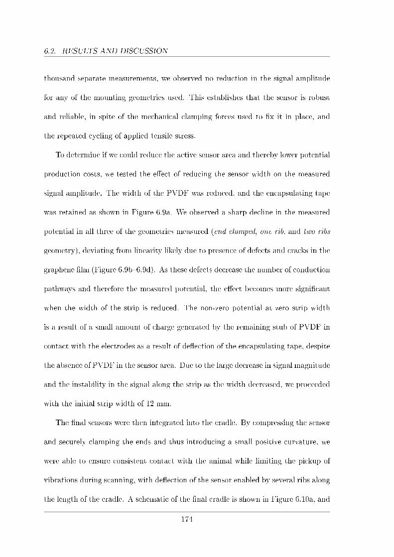
6.2. RESULTS AND DISCUSSION
thousand separate measurements, we observed no reduction in the signal amplitude
for any of the mounting geometries used. This establishes that the sensor is robust
and reliable, in spite of the mechanical clamping forces used to �x it in place, and
the repeated cycling of applied tensile stress.
To determine if we could reduce the active sensor area and thereby lower potential
production costs, we tested the e�ect of reducing the sensor width on the measured
signal amplitude. The width of the PVDF was reduced, and the encapsulating tape
was retained as shown in Figure 6.9a. We observed a sharp decline in the measured
potential in all three of the geometries measured (end clamped, one rib, and two ribs
geometry), deviating from linearity likely due to presence of defects and cracks in the
graphene �lm (Figure 6.9b�6.9d). As these defects decrease the number of conduction
pathways and therefore the measured potential, the e�ect becomes more signi�cant
when the width of the strip is reduced. The non-zero potential at zero strip width
is a result of a small amount of charge generated by the remaining stub of PVDF in
contact with the electrodes as a result of de�ection of the encapsulating tape, despite
the absence of PVDF in the sensor area. Due to the large decrease in signal magnitude
and the instability in the signal along the strip as the width decreased, we proceeded
with the initial strip width of 12 mm.
The �nal sensors were then integrated into the cradle. By compressing the sensor
and securely clamping the ends and thus introducing a small positive curvature, we
were able to ensure consistent contact with the animal while limiting the pickup of
vibrations during scanning, with de�ection of the sensor enabled by several ribs along
the length of the cradle. A schematic of the �nal cradle is shown in Figure 6.10a, and
174
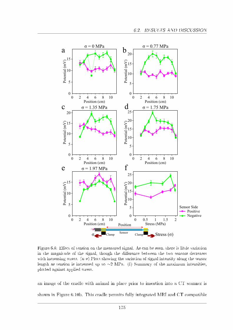
6.2. RESULTS AND DISCUSSION
0
5
10
15
20
0 2 4 6 8 10Position (cm)
Pote
nti
al (
mV
)
0
5
10
15
20
25
0 2 4 6 8 10Position (cm)
Pote
nti
al (
mV
)
0
5
10
15
0 2 4 6 8 10Position (cm)
Pote
nti
al (
mV
)
0 0.5 1 1.5 2Stress (MPa)
0
5
10
15
20
25
Pote
nti
al (
mV
)
PositiveNegative
Sensor Side
0 2 4 6 8 10Position (cm)
0
5
10
15
Pote
nti
al (
mV
)
0
5
10
15
20
0 2 4 6 8 10Position (cm)
Pote
nti
al (
mV
)
b
c d
a
e f
Position
Stress (σ)σ
σ = 1.35 MPa σ = 1.75 MPa
σ = 1.97 MPa
σ = 0.77 MPaσ = 0 MPa
SensorClamp Clamp
Figure 6.8: E�ect of tension on the measured signal. As can be seen, there is little variationin the magnitude of the signal, though the di�erence between the two sensors decreaseswith increasing stress. (a�e) Plots showing the variation of signal intensity along the sensorlength as tension is increased up to ∼2 MPa. (f) Summary of the maximum intensities,plotted against applied stress.
an image of the cradle with animal in place prior to insertion into a CT scanner is
shown in Figure 6.10b. This cradle permits fully integrated MRI and CT compatible
175
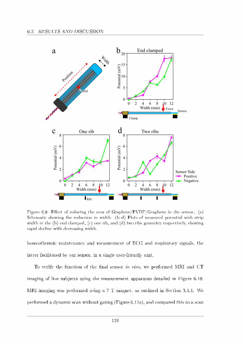
6.2. RESULTS AND DISCUSSION
Pote
nti
al (
mV
)
0 2 4 6 8 10 12Width (mm)
0
2
4
6
8
Pote
nti
al (
mV
)
0 2 4 6 8 10 12Width (mm)
0
2
4
6
8
PositiveNegative
Sensor Side
Pote
nti
al (
mV
)
0 2 4 6 8 10 12Width (mm)
0
5
10
15
20b
c d Two ribs
End clamped
One rib
Positi
on
Width
a
ForceSensor
Clamp
ForceForce
Rib
Figure 6.9: E�ect of reducing the area of Graphene/PVDF/Graphene in the sensor. (a)Schematic showing the reduction in width. (b�d) Plots of measured potential with stripwidth in the (b) end clamped, (c) one rib, and (d) two ribs geometry respectively, showingrapid decline with decreasing width.
homeothermic maintenance and measurement of ECG and respiratory signals, the
latter facilitated by our sensor, in a single user-friendly unit.
To verify the function of the �nal sensor in vivo, we performed MRI and CT
imaging of live subjects using the measurement apparatus detailed in Figure 6.10.
MRI imaging was performed using a 7 T magnet, as outlined in Section 3.4.4. We
performed a dynamic scan without gating (Figure 6.11a), and compared this to a scan
176

6.2. RESULTS AND DISCUSSION
CarbonFibre ECG
Carbon Fibre Heater Ribs
Graphene Piezo.Transducer
Mouse goes here
a b
Figure 6.10: Details of the cradle used to hold the animal. (a) Schematic of the cradledetailing key components. (b) Image of the cradle with animal in place, ready for insertioninto the CT scanner.
using our device for respiratory gating of the image acquisition (Figure 6.11b). Despite
again being able to also measure cardiac signals with our device, due to complications
with signal processing we elected only to demonstrate respiratory gating at this stage.
The two signals could simply be used in tandem, or owing to their di�erent rates could
be separated by means of band pass �lters. With reference to the average gated scan
the e�ect of respiration on the ungated image is clear, with signi�cant time dependent
movement visible across the sequential frames shown, in contrast to the good stability
of the gated images.
To show this graphically, we measured the mean pixel values across a cross-section
in the area of the liver, and plot this against time for both the ungated and gated scans
in Figure 6.11c, showing the marked increase in stability a�orded by our device. This
represents a near sevenfold reduction in the standard deviation of the mean pixel
values in this area of greatest distortion, and a twofold reduction in the standard
deviation of the overall image.
177

6.2. RESULTS AND DISCUSSION
Ungated Gated
Ungat
edG
ated
1 2 3 4 Averagea
c
b
0 5 10 15 20 25 30 35 40
Frame
3
3.5
4
Mea
n P
ixel
Val
ue 10
4
Figure 6.11: E�ect of gating on a dynamic MRI scan. Four consecutive frames taken from(a) an ungated scan and (b) a scan gated using the graphene transducer, compared to anaverage image of the four gated frames. Note blurring of ungated images, especially in thearea of the liver as highlighted in (a). (c) Mean pixel values over 20 frames for ungatedand gated scans in the area of the liver showing increase in stability with gating, with theaveraged region highlighted in inset MRI image, and location in body indicated in a 3D CTimage.
We subsequently performed high resolution image acquisition with and without
gating. These images serve to further highlight the impact of respiration on image
quality: without gating, blurring around the lungs, liver, and surrounding tissues
occurs, and signi�cant artefacts can be observed around the the body at higher con-
trast (Figure 6.12a); with gating, the image is largely free of artefacts and streaking
(Figure 6.12b). The response of the graphene sensor was largely stable throughout
178
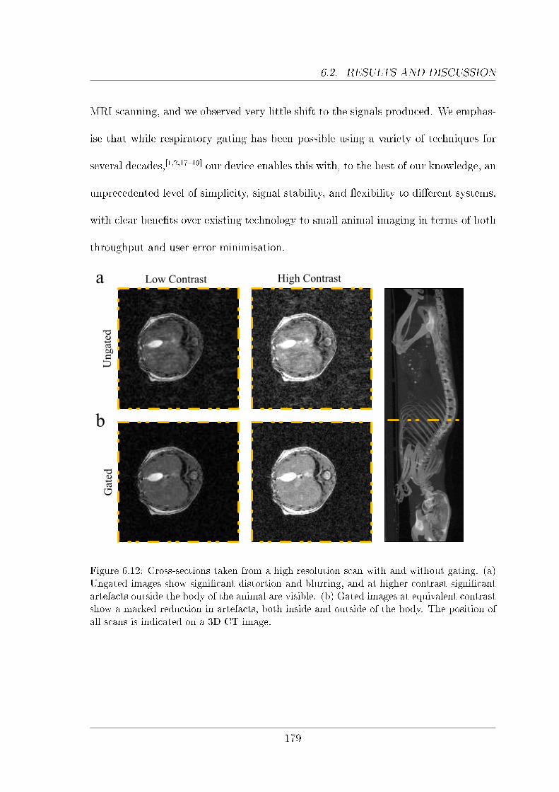
6.2. RESULTS AND DISCUSSION
MRI scanning, and we observed very little shift to the signals produced. We emphas-
ise that while respiratory gating has been possible using a variety of techniques for
several decades,[1,2,17�19] our device enables this with, to the best of our knowledge, an
unprecedented level of simplicity, signal stability, and �exibility to di�erent systems,
with clear bene�ts over existing technology to small animal imaging in terms of both
throughput and user error minimisation.
Ungat
edG
ated
High ContrastLow Contrasta
b
Figure 6.12: Cross-sections taken from a high resolution scan with and without gating. (a)Ungated images show signi�cant distortion and blurring, and at higher contrast signi�cantartefacts outside the body of the animal are visible. (b) Gated images at equivalent contrastshow a marked reduction in artefacts, both inside and outside of the body. The position ofall scans is indicated on a 3D CT image.
179

6.2. RESULTS AND DISCUSSION
We further demonstrated the utility of the device to applications requiring co-
registration by transferring the sedated animal and cradle to a CT scanner. By
removing the need to repressurise and calibrate the respiratory balloon, the cradle
can rapidly be reconnected to the new scanner's monitoring systems, with minimum
disturbance to anaesthesia and thermoregulatory systems. Body and sensor move-
ment are minimised without the need to securely clamp the animal�reducing the risk
of injury in contrast to respiratory balloons�by the secure mounting of the respirat-
ory monitor over the entirety of the bottom surface of the cradle. As a consequence,
we observed very little change in the measured respiratory signal as a result of the
transfer.
In keeping with the MRI measurements, we performed an ungated scan (Fig-
ure 6.13a), and compared this to a scan gated with the graphene contacted sensor
(Figure 6.13b). Note the blurring around the liver and the area of the thoracic cavity
highlighted in the ungated images. The graphene transducer is visible as the grey
line immediately beneath the animal.
Since its impact is much more noticeable and therefore more readily visualised
than the detuning of the magnet and smaller artefacts in MRI, here we also demon-
strate the e�ect of a silver contacted transducer on the reconstructed scan, with the
bright streaked artefacts in Figure 6.13c resulting from the strong X-ray scattering
of the sensor. The silver contacted sensor was placed on top of the animal to avoid
disturbing its posture between scans. While the e�ect of respiration on the image
quality is limited, we reiterate that our device simpli�es cradle transfer without dis-
turbing the animal's position, with the result that the resolution of the co-registered
180

6.2. RESULTS AND DISCUSSION
Gra
phen
e tr
ansd
uce
rS
ilver
tra
nsd
uce
r
YX Z
b
c
Ungat
ed
a
XX
YY
ZZ
Figure 6.13: Cross-sectional CT images showing the artefacts from the silver contactedsensor. (a�b) Images containing only the graphene sensor beneath the body: (a) ungated,artefacts highlighted; and (b) gated. (c) Images containing both the graphene and silversensors, with signi�cant artefacts visible resulting from X-ray scattering from the silvercontacted sensor. The position of each dimension is indicated on a 3D CT image.
image is enhanced. This versatility can be further extended to techniques requiring
co-registration where the stability a�orded by gating is more important, for example
181

6.2. RESULTS AND DISCUSSION
imaging techniques such as positron emission tomography,[20,21] or treatment meth-
ods like radiotherapy.[17] As in the simulated respiration measurements outlined in
Figures 6.6�6.8, we observed no reduction in the sensitivity of the device in the >20
hours of in vivo testing.
182

6.3. CONCLUSIONS
6.3 Conclusions
In conclusion, in this chapter we have demonstrated the novel application of graphene
as an ideal planar electrode material in piezoelectric respiratory monitors. This device
has clear advantages over existing technology, overcoming as it does the di�culties
with user error and the recalibration requirements of respiratory balloons, and the
MRI and CT incompatibility of silver contacted piezoelectric devices. It also has
important implications for the 3Rs of animal research (Replacement, Reduction, and
Re�nement): minimising the duration of anaesthesia by reducing transfer time in co-
registration applications, and reducing trauma and the risk of injury by removing the
need to securely clamp the animal to the sensor as is required when using respiratory
balloons.[22]
We characterised the response of the device to mechanical stimuli, and optimised
its geometry to facilitate its integration into an all carbon based monitoring and life
support cradle. We went on to test the �nished device in vivo, proving its utility in
both MRI and CT imaging, with further potential for improving other diagnostic and
also treatment techniques. Though a demonstration of this was beyond the scope
of this study, in addition to improved acquisition of the respiratory signal we also
showed that, using the same device, we could simultaneously measure cardiac signals
of su�cient magnitude to be used for gating. Several �nished devices are now in
service in the Oxford Institute for Radiation Oncology.
183
6.4. ACKNOWLEDGEMENTS
6.4 Acknowledgements
Dr Sean Smart and Mr Stuart Gilchrist were responsible for identifying de�ciencies
with the current technology that led to the inception of this device research, contrib-
uted to the device design, and developed the cradle depicted in Figure 6.10. Dr Veerle
Kersemans performed all of the in vivo MRI and CT imaging used in this study. Mr
Stuart Gilchrist provided the signal generator for respiratory simulation, and Mr Re-
uben Harding provided a number of insights and assistance in the signal conditioning
used in the non-in vivo device measurements (Figures 6.6�6.9). All graphene used
here was grown by the author.
184
Bibliography
[1] C. J. Ritchie, J. Hsieh, M. F. Gard, J. D. Godwin, Y. Kim, C. R. Crawford,�Predictive Respiratory Gating: a New Method to Reduce Motion Artifacts onCT Scans�, Radiology 1994, 190, 847�852.
[2] S. H. Bartling, J. Dinkel, W. Stiller, M. Grasruck, I. Madisch, H. U. Kauczor,W. Semmler, R. Gupta, F. Kiessling, �Intrinsic Respiratory Gating in Small-Animal CT�, European Radiology 2008, 18, 1375�1384.
[3] C. K. McKibben, N. V. Reo, �A Piezoelectric Respiratory Monitor for in vivoNMR�, Magnetic Resonance in Medicine 1992, 27, 338�342.
[4] B. A. Hargreaves, P. W. Worters, K. B. Pauly, J. M. Pauly, K. M. Koch, G. E.Gold, �Metal-Induced Artifacts in MRI�, American Journal of Roentgenology2011, 197, 547�555.
[5] A. Elster, Metal Artifact Suppression, 2018, http://mriquestions.com/metal-suppression.html (visited on 10/10/2018).
[6] J. F. Barrett, N. Keat, �Artifacts in CT: Recognition and Avoidance�, Radio-graphics 2004, 24, 1679�1691.
[7] F. E. Boas, D. Fleischmann, �CT Artifacts: Causes and Reduction Techniques�,Imaging in Medicine 2012, 4, 229�240.
[8] Viomedex, Baby Respiration Sensor: Hailsham, UK, 2018, http://www.viomedex.com/products/baby-respiration-sensor (visited on03/11/2018).
[9] Precision Acoustics, PVDF Properties and Uses, tech. rep., Precision Acous-tics, 2015, pp. 1�14.
[10] Measurement Specialties, Inc., Piezo Film Sensors Technical Manual Measure-ment, tech. rep. 1, 1999, P/N 1005663.
[11] H. Lee, I. Kim, meeree Kim, H. Lee, �Moving beyond �exible to stretchableconductive electrodes using metal nanowires and graphenes�, Nanoscale 2015,8, 1789�1822.
[12] X. Li, Y. Zhu, W. Cai, M. Borysiak, B. Han, D. Chen, R. D. Piner, L. Colomba,R. S. Ruo�, �Transfer of Large-Area Graphene Films for High-PerformanceTransparent Conductive Electrodes�, Nano Lett. 2009, 9, 4359�4363.
[13] M. E. P. Tweedie, MEng Thesis, Department of Materials, University of Ox-ford, 2014, p. 89.
185

[14] Y. Sheng, Y. Rong, Z. He, Y. Fan, J. H. Warner, �Uniformity of Large-Area Bilayer Graphene Grown by Chemical Vapor Deposition�, Nanotechno-logy 2015, 26, 395601.
[15] M. Hoop, X. Z. Chen, A. Ferrari, F. Mushtaq, G. Ghazaryan, T. Tervoort, D.Poulikakos, B. Nelson, S. Pané, �Ultrasound-Mediated Piezoelectric Di�eren-tiation of Neuron-Like PC12 Cells on PVDF Membranes�, Scienti�c Reports2017, 7, 1�8.
[16] J. Karki, Signal Conditioning Piezoelectric Sensors, Application Report SLOA033A,Texas Instruments, 2000, pp. 1�6.
[17] M. A. Hill, J. Thompson, A. Kavanagh, I. D. C. Tullis, R. G. Newman, J.Prentice, J. Beech, S. Gilchrist, S. Smart, E. Fokas, B. Vojnovic, �The De-velopment of Technology for E�ective Respiratory-Gated Irradiation Using anImage-Guided Small Animal Irradiator�, Radiation Research 2017, 188, 247�263.
[18] R. Ehman, M. McNamara, M. Pallack, H. Hricak, C. Higgins, �Magnetic Res-onance Imaging with Respiratory Gating: Techniques and Advantages�, Amer-ican Journal of Roentgenology 1984, 143, 1175�1182.
[19] V. M. Runge, J. A. Clanton, C. L. Partain, A. E. James, �Respiratory Gatingin Magnetic Resonance Imaging at 0.5 Tesla�, Radiology 1984, 151, 521�523.
[20] G. W. Goerres, E. Kamel, T. N. H. Heidelberg, M. R. Schwitter, C. Burger,G. K. Von Schulthess, �PET-CT Image Co-Registration in the Thorax: In�u-ence of Respiration�, European Journal of Nuclear Medicine 2002, 29, 351�360.
[21] J. Pascau, J. D. Gispert, M. Michaelides, P. K. Thanos, N. D. Volkow, J. J.Vaquero, M. L. Soto-Montenegro, M. Desco, �Automated Method for Small-Animal PET Image Registration with Intrinsic Validation�,Molecular Imagingand Biology 2009, 11, 107�113.
[22] P. McConville in In Vivo NMR Imaging. Methods in Molecular Biology (Meth-ods and Protocols), Vol. 771, (Eds.: L. Schröder, C. Faber), Humana Press,2011.
186

Chapter 7
Conclusions
The research presented in this thesis runs the gamut of research into 2D devices:
material synthesis, transfer techniques, device design and fabrication, and charac-
terisation. Improvements and modi�cations to the processes used to synthesise the
materials and to the fabrication techniques are outlined in Chapter 3, and when relev-
ant and requiring further explanation are presented in greater detail in Chapters 4�6.
Each of these chapters otherwise details an interrelated but largely self contained
study into 2D �exible electronics.
The successful implementation of 2D materials in �exible electronics depends on
a robust understanding of the in�uence of strain on the properties of the compon-
ent materials and their heterostructures. It is well known that weak van der Waals
bonding at an interface can lead to incomplete strain transfer between materials. In
Chapter 4, we set out to study in detail the e�ect of strain on a range of heterostruc-
tures representing device contacts, channels, and gated channels composed from boron
nitride, tungsten disulphide (WS2) and graphene on �exible poly(ethylene naphthal-
187
7. CONCLUSIONS
ate) (PEN) substrates.
In this study, we hoped initially to observe changes to the band structure using
photoluminescence (PL) spectroscopy, but instead revealed a strain release mechan-
ism that occurred independently of the heterolayer con�guration. While this led to
convolution and broadening of the PL spectra that obstructed our initial goals, we
studied this e�ect in detail and propose here a mechanism by which the strain is
released inhomogeneously during the �rst strain cycle, with the debonded �lm ex-
periencing <20 % of the applied strain in subsequent strain cycles. We veri�ed this
e�ect in all of the heterostructure permutations, and also demonstrated it after modi-
fying the PEN surface with a thin layer of poly(methyl methacrylate) (PMMA) to
increase the surface roughness and lower its modulus�revealing a similar e�ect, albeit
with a smaller total magnitude of strain transfer and broader period of debonding
during the application of strain. A complimentary study into one of the heterostruc-
tures (WS2/graphene/PEN) using Kelvin probe force microscopy helped to further
verify the mechanism, and showed corresponding shifts to the work function of both
graphene and WS2 during straining.
We went on to demonstrate a strain relaxation mechanism responsible for the
observed hysteresis between strain cycles. This hysteresis was attributed to recon-
formation of the �lm with the substrate and the relaxation of a slight residual com-
pressive strain following strain cycling, leading to a gradual blueshift over time that
was characterised over a period of ∼24 hours. Finally, we studied the e�ect of cyc-
ling the strain up to 200 times, con�rming the stabilisation of the properties after
the �rst strain cycle. We concluded that this debonding e�ect suggests the need to
188

7. CONCLUSIONS
precondition �exible devices by strain cycling before stable behaviour can be achieved.
Encouraged by the conclusions drawn in Chapter 4, we proceeded with the fab-
rication of all-2D �exible photodetector devices. Chapter 5 details the fabrication of
lateral metal-semiconductor-metal (MSM) photodetectors on PEN substrates, con-
sisting of a single crystal of WS2 contacted by graphene electrodes.
Several modi�cations were made to the fabrication techniques normally used for
rigid substrates�namely modi�cations to both the gold and graphene patterning
processes. The latter was made in response to the signi�cant damage to the sub-
strate observed at the edges of the graphene electrodes as a result of the plasma
etching. This damage was suspected as the cause of device failure at moderately low
strains, by producing stress concentrations at the sharp edges where the substrate was
etched away. A lift-o� approach for patterning graphene was developed and charac-
terised, producing similar results to the plasma etching process without damaging
the substrate. Control devices fabricated on silicon substrates showed comparable
behaviour to previous demonstrations of this device architecture that were produced
using plasma etching. This alternative approach was then used to fabricate func-
tional devices on PEN, which showed improved properties in the form of a twofold
increase in photoresponsivity during the application of strain. Unfortunately, further
application of strain led again to device failure.
Finally, in Chapter 6 the novel application of graphene in a device for cardio-
respiratory monitoring in multi-modal small animal imaging was demonstrated. The
behaviour of this device was studied in detail and its function in MRI and CT imaging
veri�ed in vivo. This device outperforms existing technology by simplifying the user
189
7.1. FUTURE OUTLOOK
experience, utilising the unique electronic and mechanical properties of graphene to
monitor the key sources of body motion and facilitate image gating, without inducing
artefacts. Image gating is made possible without complicated setup or recalibration
upon transfer of animals between di�erent pieces of equipment. This work was part
of a collaboration with the Oxford Institute for Radiation Oncology, where several
of the �nished prototypes are now in use. A patent has also been �led, in hopes of
expanding production of these sensors for supply to the pre-clinical market.
Future Outlook
While the debonding mechanism presented in Chapter 4 was universal to all of the
heterostructures and substrates in this study, this still represents a small subset of
the probable permutations and materials that we may �nd in future �exible devices.
To gain a more complete understanding of the interfacial dynamics of 2D mater-
ials, further studies would include the e�ect of other substrate materials, surface
treatments, and heterostructure con�gurations. The use of a broader range of meas-
urement techniques such as Raman, SEM or ultrasonic force microscopy to directly
image the debonded regions of the strained heterostructures would help to verify this
mechanism. Finally, a greater focus on strain distribution with a more extensive use
of mapping (beyond the scope of this study due to equipment limitations) would be
valuable. Though there is still much to discover, this work contributes to the growing
body of knowledge on friction in 2D materials, with important rami�cations for their
implementation in �exible devices.
Although the �exible photodetectors demonstrated in Chapter 5 ultimately failed
190
7.1. FUTURE OUTLOOK
in response to strain, there are a number of important details revealed by this work
that have implications for the �eld of 2D microelectronics. The lift-o� patterning
approach detailed in this chapter is a fairly new approach that could �nd application
in producing both rigid and �exible devices since it removes the requirement that
underlying layer(s) must be protected during patterning, be it a 2D material, polymer,
or another plasma sensitive material. This patterning approach could be extended to
produce vertically heterostructured �exible devices that may have more favourable
performance than those demonstrated here.
The transient increase in photocurrent observed in the lift-o� patterned devices
during straining indicates that, as is the case with conventional semiconductors, strain
engineering is an approach that can lead to signi�cantly enhanced device properties�
if it can be controllably applied. Finally, this study reveals that additional design
considerations must be made to protect 2D devices from the deleterious e�ect of
strain, perhaps by device encapsulation or the introduction of a compressive strain
during fabrication, approaches that were not explored here but may be essential for
2D materials to be viable in this application. To ascertain the exact nature of device
failure in the lift-o� patterned devices, conductive AFM or in situ SEM would both
be viable techniques to reveal the location and mechanism of failure.
Implementation of the cardio-respiratory monitor technology demonstrated in
Chapter 6 is already underway, but as with all 2D devices a major di�culty lies
in scaling production up from the laboratory. As such, future work will involve de-
termining how to produce the devices on a larger scale, as well as studying possible
improvements to the device design. Additionally, though we are con�dent of its utility
191
7.1. FUTURE OUTLOOK
throughout the �eld of small animal imaging, a complete demonstration of the func-
tion of the device in other imaging and treatment techniques would be valuable�a
comprehensive and conclusive demonstration of the superiority of a novel technology
being a prerequisite for successful disruption of the existing one.
192