
Molecular Engineering of Semiconducting Polymers for ...
227
Molecular Engineering of Semiconducting Polymers for Perovskite Solar Cells PhD Thesis Silvia Valero Moya Supervised by Dr. Juan Luis Delgado Cruz Dr. Aurelio Mateo-Alonso Donostia-San Sebastián 2019 (cc)2019 SILVIA VALERO MOYA (cc by-nc 4.0)
-
Upload
khangminh22 -
Category
Documents
-
view
0 -
download
0
Transcript of Molecular Engineering of Semiconducting Polymers for ...

Molecular Engineering of Semiconducting
Polymers for Perovskite Solar Cells
PhD Thesis
Silvia Valero Moya
Supervised by
Dr. Juan Luis Delgado Cruz
Dr. Aurelio Mateo-Alonso
Donostia-San Sebastián
2019
(cc)2019 SILVIA VALERO MOYA (cc by-nc 4.0)


A mi Familia

Contents
I
CONTENTS
1. INTRODUCTION ........................................................................... 1
1.1 Energy Supply and Climate Change .................................................. 3
1.2 Photovoltaic Energy Conversion ......................................................... 6
1.2.1 Basics of Semiconductors ......................................................................... 6
1.2.2 Principles of Solar Cells .......................................................................... 10
1.2.3 Current-Voltage Characteristics of Solar Cells ....................................... 12
1.3 Types of Solar Cells ............................................................................ 13
1.3.1 Wafer-Based Solar Cells ......................................................................... 14
1.3.2 Thin-Film Solar Cells .............................................................................. 16
1.4 Dye-Sensitized Solar Cells ................................................................. 19
1.5 Perovskite Solar Cells ........................................................................ 21
1.5.1 Historical Development of Perovskite Solar Cells ................................. 21
1.5.2 Hybrid Organic-Inorganic Perovskite Materials ..................................... 22
1.5.3 Working Principle and Device Structures ............................................... 25
1.6 Obstacles towards Large-Scale Application of PSCs ...................... 28
1.6.1 Long-Term Stability ................................................................................ 28
1.6.2 Toxicity of Lead ...................................................................................... 31
1.6.3 Hysteresis ................................................................................................ 31
1.6.4 Scale up ................................................................................................... 32
2. DOPANT-FREE HOLE-TRANSPORTING POLYMERS FOR
PEROVSKITE SOLAR CELLS ............................................................. 35
2.1 Introduction ........................................................................................ 37

Contents
II
2.1.1 Role and Properties of Hole-Transporting Materials in PSCs ............... 37
2.1.2 Hole-Transporting Materials for PSCs ................................................... 39
Spiro-Structured Hole-Transporting Materials ................................ 39
Hole-Transporting Polymers for PSCs ............................................. 41
2.1.3 Efficient Dopant-Free Hole-Transporting Polymers for PSCs .............. 44
2.2 Objectives .............................................................................................47
2.3 Results and Discussion ........................................................................48
2.3.1 Design and Synthesis of Polymers P1-P6 .............................................. 48
Synthesis of Functionalized Monomers ........................................... 49
Synthesis of Polymers P1-P6 ............................................................ 52
2.3.2 Thermal, Optical and Electrochemical Properties ................................. 56
2.3.3 Perovskite Solar Cells Employing Polymers P1-P6 ............................... 60
Perovskite-Based Device Fabrication............................................... 61
Photovoltaic Device Testing ............................................................. 62
Stability of Perovskite Solar Cells .................................................... 64
2.4 Conclusions ..........................................................................................66
3. PERFLUORINATED ADDITIVES FOR PEROVSKITE SOLAR
CELLS ................................................................................................. 67
3.1 Introduction .........................................................................................69
3.1.1 Additive Engineering to Improve the Perovskite Layer ........................ 69
Semiconducting Chemical Additives ............................................... 72
Fluorinated Additives for Perovskite Solar Cells ............................. 74
3.2 Objectives .............................................................................................78
3.3 Results and Discussion ........................................................................79
3.3.1 Design and Synthesis of Additives S1, P7 and P8 ................................. 79

Contents
III
Synthesis of Intermediates ............................................................... 80
Synthesis of Additives S1, P7 and P8 .............................................. 81
3.3.2 Thermal, Optical and Electrochemical Properties .................................. 86
3.3.3 Perovskite Solar Cells Employing S1, P7 and P8 ................................... 90
Perovskite-Based Device Fabrication .............................................. 90
Photovoltaic Device Testing ............................................................ 91
Film Characterization ....................................................................... 94
Stability Tests ................................................................................... 99
3.4 Conclusions ....................................................................................... 101
4. ELECTRON-TRANSPORTING POLYMERS FOR PEROVSKITE
SOLAR CELLS .................................................................................. 103
4.1 Introduction ...................................................................................... 105
4.1.1 Role and Properties of Electron-Transporting Materials in PSCs ........ 105
4.1.2 Organic Electron-Transporting Materials for PSCs .............................. 106
4.1.3 Naphthalene diimide-Based ETMs in PSCs ......................................... 109
NDI-Based Small Molecules as ETMs in PSCs ............................ 109
NDI-Based Polymers as ETMs in PSCs ........................................ 110
4.2 Objectives .......................................................................................... 113
4.3 Results and Discussion ..................................................................... 114
4.3.1 Design of Novel NDI-Based Polymers ................................................. 114
Synthesis of Model Compounds MC1-MC3 .................................. 115
Optical, Electrochemical and Charge Transport Properties of Model
Compounds MC1-MC3 ................................................................................... 116
4.3.2 Synthesis of NDI-Based Polymers P9-P11 ........................................... 120
Synthesis of Functionalized Monomers ......................................... 120
Synthesis of Polymers P9-P11 ....................................................... 121

Contents
IV
4.3.3 Thermal, Optical and Electrochemical Properties ............................... 125
4.4 Conclusions ........................................................................................130
5. EXPERIMENTAL SECTION ...................................................... 131
5.1 General Methods and Materials ......................................................133
5.1.1 Nuclear Magnetic Resonance Spectroscopy ........................................ 133
5.1.2 Mass Spectrometry ............................................................................... 133
5.1.3 Size Exclusion Chromatography .......................................................... 134
5.1.4 Water Contact Angle Measurements.................................................... 134
5.1.5 Thermal Analysis ................................................................................. 134
5.1.6 Absorption and Fluorescence Spectroscopy ........................................ 134
5.1.7 Cyclic Voltammetry ............................................................................. 135
5.1.8 Time-Resolved Microwave Conductivity ............................................ 135
5.1.9 Scanning Electron Microscopy ............................................................ 135
5.1.10 Atomic Force Microscopy .................................................................... 136
5.1.11 X-Ray Diffraction................................................................................. 136
5.2 Synthesis .............................................................................................136
5.2.1 Dopant-Free Hole-Transporting Polymers for PSCs ........................... 136
Synthesis of Precursors 1-8 ............................................................ 136
Synthesis of Monomers M1-M5 ..................................................... 142
Synthesis of Polymers P1-P6 .......................................................... 146
5.2.2 Perfluorinated Additives for PSCs ....................................................... 153
Synthesis of Precursors 9 and 10 .................................................... 153
Synthesis of Monomers M6-M7 and Intermediate 11 .................... 155
Synthesis of Additives S1, P7 and P8 ............................................ 157
5.2.3 Electron-Transporting Polymers for PSCs ........................................... 160

Contents
V
Synthesis of Model Compounds MC1-MC3 .................................. 160
Synthesis of Precursors 12-14 ........................................................ 163
Synthesis of Monomers M8-M10 .................................................. 165
Synthesis of Polymers P9-P11 ....................................................... 168
5.3 Construction and Testing of Perovskite Solar Cells ..................... 171
5.3.1 Perovskite Solar Cells Employing P1-P6 as HTMs .............................. 171
Device Fabrication ......................................................................... 171
Device Characterization ................................................................. 172
5.3.2 Perovskite Solar Cells Employing S1 and P7 as Additives .................. 173
Device Fabrication ......................................................................... 173
Device Characterization ................................................................. 174
6. SUMMARY/RESUMEN ............................................................. 177
6.1 Summary ........................................................................................... 179
6.2 Resumen ............................................................................................ 185
7. REFERENCES ........................................................................... 191
ACKNOWLEDGEMENTS ................................................................... 211


Abreviations and symbols
VII
Abbreviations and Symbols
In addition to the standard abbreviations, acronyms and symbols in organic
chemistry, defined in the Journal of Organic Chemistry author guidelines, the following
terms have been also used in this manuscript:
AcOH Acetic acid
AcOEt Ethyl acetate
AFM Atomic force microscopy
a:Si-H Hydrogenated amorphous silicon
a.u. Arbitrary units
BDT Benzo[1,2-b:4,5:b´]dithiophene
BHJ Bulk heterojunction
BT 2,1,3-Benzothiadiazole
CB Conduction band
CIGS Copper indium gallium diselenide
c-TiO2 Compact TiO2
COD 1,5-Cyclooctadiene
CQD Colloidal quantum dot
CZTS Copper zinc tin sulfide
c-Si Crystalline silicon
CV Cyclic voltammetry
DBDMH 1,3-Dibromo-5,5-dimethylhydantoin
DCM Dichloromethane
DMF N,N-Dimethylformamide
Dba Dibenzylideneacetone
DMSO Dimethyl sulfoxide
dppf 1,1’-Bis(diphenylphosphino)ferrocene
dppp 1,3-Bis(diphenylphosphino)propane
dtbpy 4,4′-Di-tert-butyl-2,2′-bipyridine
DSSCs Dye-sensitized solar cells
DSC Differential scanning calorimetry
Ɛ Molar extinction coefficient
Eg Energy gap
EHOMO HOMO energy
ELUMO LUMO energy
EonsetOx1 Onset potential of the first oxidation
E1/2Ox1 Half wave potential of the first oxidation

Abreviations and Symbols
VIII
ESI Electrospray ionization
ETL Electron-transporting layer
ETM Electron-transporting material
EtOH Ethanol
e- Electron
FA Formamidinium
Fc Ferrocene
Fc+ Ferrocinium
FF Fill factor
FK102 Tris[2-(1H-pyrazol-1-yl)pyridine)]cobalt(III)tris(hexafluorophosphate)
FK209 Tris[2-(1H-pyrazol-1-yl)-4-tert-butylpyridine]-cobalt(III)-tris[bis(tri-
fluoromethylsulfonyl)imide]
FTO Fluorine-doped tin oxide
GBs Grain boundaries
h+ Hole
HI Hysteresis index
HOMO Highest occupied molecular orbital
HTL Hole-transporting layer
HTM Hole-transporting material
I Current
ITO Indium tin oxide
J Current density
JSC Short-circuit current
Li-TFSI Lithium bis[(trifluoromethyl)sulfonyl]amide
LUMO Lowest unoccupied molecular orbital
MA Methylammonium
MALDI Matrix-assisted laser desorption/ionization
mc-Si Multiple crystalline silicon
MeOH Methanol
m-TiO2 Mesoporous TiO2
MJ Multijunction
Mn Number-average molecular weight
MPP Maximum power point
Mw Weight-average molecular weight
NBS N-Bromosuccinimide
NDI Naphthalene diimide
NDA 1,4,4,8-Naphthalenetetracarboxylic dianhydride

Abreviations and symbols
IX
NMR Nuclear magnetic resonance
OLEDs Organic light-emitting diodes
OFETs Organic field-effect transistors
OSCs Organic solar cells
PCBM [6,6]-Phenyl-C61-butyric acid methyl ester
PCBTDPP Poly[N-90-heptadecanyl-2,7carbazole-alt-3,6-bis(thiophen-5-yl)-2,5-
dioctyl-2,5-dihydropyrrolo[3,4] pyrrole-1,4-dione]
PCPDTBT Poly{2,6-[4,4-bis-(2-ethylhexyl)-4H-cyclopenta[2,1-b;3,4-b’]dithiophene]-
alt-4,7(2,1,3-benzothiadiazole)}
PCDTBT Poly[N-9’-heptadecanyl-2,7-carbazole-alt-5,5-(4’,7’-di-2-thienyl-2’,1’,3’-
benzothiadiazole)]
PCE Power conversion efficiency
PDI Polydispersity
PEG Poly-ethylene glycol
PDPPDBTE Poly[2,5-bis(2-decyldodecyl) pyrrolo[3,4-c]pyrrole-1,4(2H,5H)-dione-(E)-
1,2-di(2,2’-bithiophen-5-yl)ethene]
PDPP3T Poly{2,2'-[(2,5-bis(2-hexyldecyl)-3,6-dioxo-2,3,5,6-tetrahydropyrrolo[3,4-
c ]pyrrole-1,4-diyl)dithiophene]-5,5'-diyl-alt-thiophen-2,5-diyl}
PE Petroleum ether
PEDOT:PSS Poly(3,4-ethylenedioxythiophene):polystyrene sulfonate
P3HT Poly (3-hexylthiophene-2,5-diyl)
Pin Power input
Pmax Power output
PSCs Perovskite solar cells
PTAA Poly[bis(4-phenyl)(2,4,6-trimethyl)amine]
rpm Revolutions per minute
rps Revolutions per second
Rs Series resistance
sc-Si Single crystalline silicon
SEC Size exclusion chromatography
SEM Scanning electron microscopy
spiro-
OMeTAD 2,2’,7,7’-tetrakis(N,N-di-p-methoxyphenylamine)-9-9’ spirobifluorene
ss-DSSCs Solid-state dye-sensitized solar cells
TBAHFP Tetrabutylammonium hexafluorophospate
TRMC Time-resolved microwave conductivity
tBP 4-tert-butylpyridine
TLC Thin layer chromatography

Abreviations and Symbols
X
Td Decomposition temperature
Tg Glass transition temperature
Tm Melting temperature
TGA Thermogravimetric analysis
THF Tetrahydrofuran
TOF Time of flight
TPD N,N′-diphenyl-N,N′-bis-(3-methylphenyl)-N,N′-bis(phenyl)benzidine
UV-vis Ultraviolet-visible
VB Valence band
V Voltage
VOC Open-circuit voltage
Xn Degree of polymerization
XRD X-ray diffraction
λ Wavelength
φΣμ Pseudo-photoconductivity
μ Mobility
σ Conductivity

1. INTRODUCTION


1.1 Energy Supply and Climate Change
3
1 INTRODUCTION
1.1 Energy Supply and Climate Change
Since the discovery of fire by primitive humans, mankind has been searching
ways to take advantage of different energy sources. Before the industrial revolution,
wood was the primary energy source, which was used not only to fabricate buildings
and homes at that time, but also for heating, cooking and other basic needs for survival.
In addition, wind, water, tide etc. have been exploited as energy sources and are still
used to power machines in many parts of the world.
However, since the industrial revolution and especially over the last decades,
the consumption of energy has undergone an unprecedented change and nowadays, our
current energy system is dominated by fossil fuels.[1]
Fossil fuels, including coal, oil and natural gas, are currently the world´s primary
energy source (energy directly harvested from natural resources). They were formed
millions of years ago when dead plants and animals were buried by sand and water and
were subjected to intense heat and pressure. However, fossil fuels are considered non-
renewable energy sources because they do not naturally replenish on a short enough
timescale for humans to use.
In order to extract energy from fossil fuels they have to be burned. This process
mainly releases carbon dioxide (CO2) into the atmosphere together with other
greenhouse gases. Those gases, trap heat prompting the raise in Earth´s temperature
and are considered by scientists the main reason for the climate change.[2]
The role of energy is vital for the modern industrial economy and the
consumption of energy is linked with the economic prosperity and social progress.
However, over the last decades, population growth together with the raise of industrial
production have resulted in a large increase in energy consumption. This has resulted
in a drastic growth of the CO2 concentration in the atmosphere caused by the extensive
use of fossil fuels.[2] This concentration has changed from the stable value in recent

1 Introduction
4
history, about 275 ppm, up to 413 ppm in 2019 in just 200 years, leading to serious
environmental issues (Figure 1).[3]
Figure 1. Atmospheric CO2 concentration variation measured at Mauna Loa observatory (Hawaii).
There are strong indications suggesting that the climate is changing and as a
result, observable phenomena are appearing. Global temperature rise, warming oceans,
glaciers retreat, less snow cover, sea level rise, declining arctic sea ice (Figure 2),
extreme events or ocean acidification are some of the phenomena related to the climate
change caused by the fossil fuels consumption.[4–6]
Figure 2. The area of the Arctic Ocean covered in ice increases during the winter and then shrinks
during the summer. These images compare the 1984 minimum (left) with that of 2012 (right). A long-
term downward trend of about 12 percent sea-ice loss per decade since the late 1970s has been
observed.[7]
The situation expected for the near future is not promising. In fact, by 2040 is
expected an increase in the world population from 7.4 billion to more than 9.2 billion
people. This growth together with industrial energy needs will result in an increase in
the energy demand (Figure 3).[8,9]

1.1 Energy Supply and Climate Change
5
Figure 3. World energy consumption will rise 28% between 2015 and 2040.[9]
Nevertheless, what would happen if we burn the Earth's entire supply of fossil
fuels or if we continue burning fossil fuels at that rate?
The environmental problem is threatening the Earth and humanity is becoming
aware of this. In fact, 195 countries signed the Paris Agreement in 2015 to fight against
the climate change. To this end, these countries committed themselves to take the
necessary measures to keep the temperature rise during this century to no more than
2 ºC above the levels from the pre-industrial era (1850-1900).[10] For example, the
European Union has set a greenhouse gases emissions reduction targets of 20, 30 and
80% by 2020, 2030 and 2080, respectively, relative to the levels existing in 1990.[11]
To achieve these targets, and considering the limited amount of non-renewable
fossil fuels and the environmental impact of their use, a transition to a carbon-free
world is compulsory. It will be strongly imperative a huge shift to lower-emission
energy sources by developing new forms of clean, environmentally friendly and
sustainable energy technologies.[12] That means a shift to renewables, which nowadays
only constitute an 11% (Figure 4) of the total world energy consumption.[13]
Figure 4. World energy consumption by energy source, 2017.
4% 11%
28%23%
34%Nuclear energy
Renewables
Coal
Natural gas
Petroleum

1 Introduction
6
1.2 Photovoltaic Energy Conversion
“I would put my money on the sun and solar energy. What a source of power! I
hope we do not have to wait until oil and coal run out before we tackle that”
Thomas Edison, 1931.[14]
As a matter of fact, solar energy is, together with wind energy, one of the best
alternatives to fossil fuels.[15] Solar energy is the most abundant, clean and easily
accessible renewable energy available, which could meet the energy needs of
humankind. In fact, the sun energy that reaches earth surface every minute is enough
to satisfy the world´s energy demand for a whole year if efficient conversion of solar
energy to electricity is ensured. Therefore, designing systems that can effectively
gather, transfer, or store solar energy has been a great and enduring challenge for
researchers.[16]
1.2.1 Basics of Semiconductors
Although this thesis focuses on the synthesis of organic semiconductors for
application in perovskite solar cells, this section will focus on some basic concepts
related to classical inorganic semiconductors, which are essential to understand the
principles of solar cells. To explain better the general characteristics and phenomena
in semiconductors, in some cases we will use silicon semiconductors as an example.
Organic semiconductors show differences compared to conventional inorganic
semiconductors but their physics is similar to that of classical inorganic
semiconductors.[15]
Band structure, electrons and holes
Semiconductors exhibit conductivity, which is situated in the range between
conductors and insulators. Furthermore, conductivity in semiconductors can vary
depending on the environment. This ability makes semiconductors crucial in the
fabrication of electronic devices.

1.2 Photovoltaic Energy Conversion
7
Inorganic semiconductors are made up of individual atoms bonded together in a
regular periodic structure to form a crystal lattice. In the case of silicon semiconductors,
each atom is surrounded by 8 electrons, which are all taking part in covalent bonds
(Figure 5).
Figure 5. Schematic representation of Si-crystal.
Under certain conditions, the electrons could gain enough energy to escape from
their bonds and they would be capable of moving in the whole crystal. In that situation,
they behave as free electrons and as a result, they will be able to participate in
conduction. The aforementioned free electrons are in a high-energy state, while
electrons which cannot move, are in a low-energy state. Electrons cannot attain energy
values in between these two energy states and consequently, they are at a low-energy
position in the bond, or they have enough energy to move free. When the electron is
excited to a high-energy state, it leaves also an empty “space” in the low-energy state.
The space left behind by electrons allow a covalent bond to move from one electron to
another, thus appearing to be a positive charge moving through the crystal lattice. This
empty space is commonly called a hole (h+), and it is similar to an electron (e-), but
with a positive charge.[17] Electrons and holes are the charge carriers in semiconductors.
The aforementioned energy that is required for an electron to break free is called
band gap (Eg). Generally, Eg is defined as the energy difference between the highest
occupied energy level called “valence band” (VB) and the lowest unoccupied energy
level called “conduction band” (CB). Depending on the energy gap, materials in
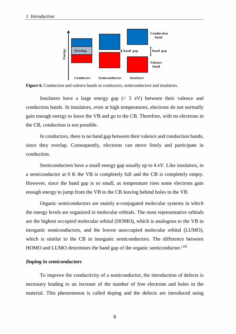
electronics can be classified into conductors, insulators and semiconductors (Figure 6).
SiSiSi
SiSiSi
SiSiSi
1 Introduction
8
Figure 6. Conduction and valence bands in conductors, semiconductors and insulators.
Insulators have a large energy gap (> 5 eV) between their valence and
conduction bands. In insulators, even at high temperatures, electrons do not normally
gain enough energy to leave the VB and go to the CB. Therefore, with no electrons in
the CB, conduction is not possible.
In conductors, there is no band gap between their valence and conduction bands,
since they overlap. Consequently, electrons can move freely and participate in
conduction.
Semiconductors have a small energy gap usually up to 4 eV. Like insulators, in
a semiconductor at 0 K the VB is completely full and the CB is completely empty.
However, since the band gap is so small, as temperature rises some electrons gain
enough energy to jump from the VB to the CB leaving behind holes in the VB.
Organic semiconductors are mainly π-conjugated molecular systems in which
the energy levels are organized in molecular orbitals. The most representative orbitals
are the highest occupied molecular orbital (HOMO), which is analogous to the VB in
inorganic semiconductors, and the lowest unoccupied molecular orbital (LUMO),
which is similar to the CB in inorganic semiconductors. The difference between
HOMO and LUMO determines the band gap of the organic semiconductor.[18]
Doping in semiconductors
To improve the conductivity of a semiconductor, the introduction of defects is
necessary leading to an increase of the number of free electrons and holes in the
material. This phenomenon is called doping and the defects are introduced using
band gap
Conduction
band
Valence
band
band gap
Conductor Semiconductor Insulator
Overlap
En
erg
y

1.2 Photovoltaic Energy Conversion
9
dopants. A semiconductor that is not doped is called intrinsic semiconductor and it has
a high degree of purity but low conductivity.
When an intrinsic Si semiconductor is doped with impurity atoms that have one
electron more than Si in the outer electronic shell, e.g. phosphorous (P), this results in
more electrons than holes in the crystal lattice. These extra electrons can move freely
in the semiconductor. Because electrons are negatively charged, such doped
semiconductor is called n-type (Figure 7 left). Similarly, when an intrinsic Si
semiconductor is doped with impurity atoms that have one electron less than Si in the
outer electronic shell, e.g. boron (B), there will be more holes than electrons in the
crystal. Since holes are positively charged, such semiconductor is then called p-type
(Figure 7 right).[17] Doped semiconductors are called extrinsic semiconductors.
Figure 7. Schematic representation of Si-crystal doped with P to produce n-type semiconductors (left)
and Si-crystal doped with B to produce p-type semiconductors (right).
Light absorption in semiconductors
Semiconductors are responsible for absorbing light in a solar cell. However,
these materials are only able to absorb light of the solar spectrum with energy equal to
or higher than their band gap. If the incident light has energy higher than the band gap
of the semiconductor, part of the light is absorbed but the excess of energy will be lost
in the form of heat. If the light energy is lower than the band gap, the semiconductor
will not absorb this light. Since the solar spectrum encompasses photons with different
energies which cannot be absorbed by a single semiconductor, a huge part of the energy
is lost.[19] These losses are closely related to the maximum obtainable efficiency of
SiSiSi
SiPSi
SiSiSi
extra
electron
SiSiSi
SiBSi
SiSiSi
holemissing
electron

1 Introduction
10
solar cells, which is determined by the band gap of the semiconductor, as is shown in
Figure 8.
Figure 8. Maximum theoretical efficiency for a solar cell operated at 298.15 K and illuminated with
the AM 1.5G spectral irradiance as a function of the band gap energy.[20]
In fact, solar cells with only one semiconductor have a maximum theoretical
efficiency of 33.2%, which requires a semiconductor band gap of 1.34 eV.[20,21]
1.2.2 Principles of Solar Cells
When we talk about solar or photovoltaic cells we are referring to devices able
to convert sunlight into electricity. These devices are usually integrated in larger
structures called photovoltaic or solar modules. Each solar cell works taking the energy
from the sun and converting it into electricity due to the photovoltaic effect.
The photovoltaic effect was discovered by Edmond Becquerel in 1839. He
showed that when exposing certain materials (semiconductors) to sunlight they could
generate electrical current. This effect is the basis not only of the majority of solar cells,
but also many other electronic devices.[22]
A solar cell is created when p-type and n-type semiconductor materials come
together forming a p-n junction. Figure 9 shows a schematic of the p-n junction.
Figure 9. A schematic of the semiconductor p-n junction at equilibrium.
Band gap (eV)
Eff
icie
nc
y(%
)

1.2 Photovoltaic Energy Conversion
11
By joining these two types of semiconductors, extra electrons in the n-type
semiconductor diffuse to the p-type semiconductor because the electron concentration
in the n-type is higher than in the p-type semiconductor. Similarly, extra holes in the
p-type semiconductor diffuse to the n-type semiconductor. When electrons and holes
move across the junction, they leave behind charged particles. These charged particles
are not able to move because they are taking part of the crystal lattice. In this way,
positively charged particles stay at the n-side and negatively charged particles remain
at the p-side of the junction. The process continues until eventually a state of
equilibrium is achieved and an electric field (E) forms. This electric field acts as a
“potential barrier” at the junction keeping away any free charge carrier from passing
through the junction.[23]
If the p-n junction is connected to an external circuit and a positive voltage is
applied to the p-type side and a negative voltage to the n-type side (forward bias), free
charges will be able to overcome the potential barrier and move to the corresponding
side of the junction. The charges driven round the circuit form an electric current and
do useful work (Figure 10).[24]
Figure 10. A schematic representation of the semiconductor p-n junction connected through an
external circuit.
Solar cells are essentially illuminated p-n junctions. When light shines on them
with an energy larger than the band gap of the semiconductor, an electron from the VB
will be excited to the CB. Consequently, an electron in the CB and a hole in the VB,
named as e-/h+ pair, will be generated. If these mobile charge carriers reach the vicinity
of the junction, the electric field will push holes into the p-side and electrons into the
n-side.

1 Introduction
12
If both sides of the junction are connected through an external circuit, the
accumulated electrons in the n-side will flow out of the n-side and will go to the p-side
to recombine with the holes and current will be generated.
Essentially, three steps are necessary to transform sunlight into electricity in any
photovoltaic device: 1) absorption of sunlight; 2) formation of free charges (electrons
and holes), and 3) collection of charges at the respective electrodes.[25]
1.2.3 Current-Voltage Characteristics of Solar Cells
One of the most important characterization techniques for solar cells is the
current density-voltage (J-V) measurements, from which the solar cell energy
conversion can be determined (Figure 11). The J-V characteristics are monitored by
changing the external voltage from zero (short-circuit conditions) to infinite voltage
(open-circuit conditions), or by changing the external voltage in the opposite
direction.[24]
Figure 11. Current density-voltage curve of a solar cell under light illumination.
The power conversion efficiency (PCE) or efficiency (η) of any solar cell is
defined as the ratio of energy output (Pmax) from the solar cell to input (Pin) energy
from the sun (Equation 1):
η = Pmax
Pin
= FF ∙ VOC ∙ JSC
Pin
(1)

1.3 Types of Solar Cells
13
The key solar cell parameters are:
- Short-circuit current (JSC). It is the maximum current from a solar cell that is
recorded when the voltage across the cell is zero.
- Open-circuit voltage (VOC). It is the maximum voltage available from a solar
cell, and this occurs at zero current.
- Fill factor (FF). It is defined as the ratio of the maximum power from the solar
cell to the product of VOC and JSC (Equation 2):
FF = A
B=
Pmax
VOC∙ JSC
= Vmax ∙ J max
VOC∙ JSC
(2)
1.3 Types of Solar Cells
Depending on the device structure and architecture, photovoltaic technologies
can be divided into two main groups (Figure 12):
- Wafer-based solar cells, which are produced from slices of semiconducting
wafers. They are used directly without the necessity of using any substrate. However,
wafers are typically covered with glass for mechanical stability and protection.
- Thin-film solar cells, which are produced by depositing thin layers of
semiconductors onto a glass, metal or plastic foil substrate. These, in turn, are divided
into commercial and emerging thin-film solar cells.[26]
Figure 12. Classification of solar cells technologies based on device structure.[26]
CIGSCdTe
Quantum dotDSSCOrganicPerovskite
CZTSa-Si:H
20µm
III-V MJ GaAsc-Si
Wafer Thin film

1 Introduction
14
1.3.1 Wafer-Based Solar Cells
Currently, wafer-based solar cells can be categorized into crystalline silicon (c-
Si), gallium arsenide (GaAs) and multijunction (MJ) solar cells, which are all
commercially available.
Crystalline silicon (c-Si) solar cells
About 90% of the world´s solar cells are made from wafers of crystalline
silicon.[27] They can be made either of single crystal [single crystalline silicon (sc-Si)
solar cells] or contain many small grains of silicon crystals [multiple crystalline silicon
(mc-Si) solar cells] as shown in Figure 13.[28] Currently, the best efficiency for sc-Si
solar cells and mc-Si solar cells are 26.7% and 22.3%, respectively. For large-area
modules, records efficiencies are 24.4% and 19.9% for sc-Si and mc-Si,
respectively.[29]
A) B) C)
Figure 13. A) Single crystalline silicon-based solar panel, B) Single crystalline silicon solar cell and
C) Multiple crystalline silicon solar cell.
A key disadvantage in c-Si solar cells is that crystalline silicon is a poor
absorber, which requires the use of thick and rigid wafers. This leads to a limitation in
terms of flexibility and modules design. In addition, the high level of material´s purity
required, makes their manufacturing process slow and labour-intensive, which makes
them very expensive.[30]
Despite these limitations, they are still the predominant photovoltaic technology
because of their high photo-conversion efficiency, high stability, proven
manufacturability, abundant materials, non-toxicity, long lifespan and reliable
performance, among others.[28,30]

1.3 Types of Solar Cells
15
Gallium arsenide (GaAs) solar cells
Gallium arsenide (GaAs)-based photovoltaic cells are produced by depositing
layers of gallium and arsenic onto a base of single crystal GaAs.[31]
GaAs is the highest efficiency solar material currently available in the world.
GaAs single junction solar cells have achieved the highest power conversion
efficiencies of any material system (29.1% for lab cells and 25.1% for modules).[29]
However, the high cost of GaAs solar cells has restricted their use in large-scale
terrestrial applications and they are only used in applications in which high efficiencies
are crucial, such as outer space exploration.
Both silicon and GaAs solar cells, discussed above, are known as single junction
solar cells, since there is only one p-n junction in the device. To overcome the limitation
of a single absorber, a multiple junction structure is proposed, in which several
materials with different band gaps are used.
Multijunction (MJ) solar cells
The aim of multijunction or tandem solar cells is to use a combination of
semiconductor materials, meaning several single p-n junctions, with different band
gaps and stack them together. Each single junction would grew on top of each other
and to ensure optimal absorption, top junctions should have higher band gaps than
bottom junctions. In this way, the light passes first through a material which absorbs
the high-energy photons and then lower-energy photons will be absorbed by the
junctions at the bottom.[19]
A typical MJ solar cell uses two or more absorbing junctions, and the theoretical
maximum efficiency increases with the number of junctions. They are semiconductor
alloys that incorporate elements of the groups III and V of the periodic table such as
gallium indium phosphate (GaInP), gallium indium arsenide (GaInAs) or gallium
arsenide (GaAs).
This class of solar cells are produced in the same way as GaAs cells, i.e.
depositing layers of material onto a single crystal base, which makes them very

1 Introduction
16
expensive to produce, and only commercially viable for concentrated photovoltaic
systems and space applications.[28] MJ solar cells are the most efficient solar cells ever
developed with demonstrated efficiencies above 40% (38.8% for a solar cell with 5
junctions under 1 sun illumination and 46.0% for a triple junction solar cell under 508
suns).[29]
1.3.2 Thin-Film Solar Cells
Thin-film solar cells offer a wide variety of choices in terms of device design
and fabrication, constituting about 10% of the global market.[26] They are cheaper to
produce than wafer-based solar cells, not only because the amount of raw materials
needed to produce the solar cell is smaller but also their fabrication requires less energy,
since solar cells can grow themselves on top of a substrate. However, they are less
efficient than wafer-based solar cells.
A) Commercial Thin-film Solar Cells
The three most widely commercialized thin-film solar cells include
hydrogenated amorphous silicon (a:Si-H), cadmium telluride (CdTe) and copper
indium gallium diselenide (CIGS) solar cells. Common among the three materials is
their direct band gap, meaning that it is possible to make much thinner solar cells out
of the materials, so they can be used through flexible layers for instance.[27,32]
Hydrogenated amorphous silicon (a:Si-H) solar cells
Hydrogenated amorphous silicon material has been used for the fabrication of
solar cells because of their extensive variety of points of interest, such as high
absorption coefficient (higher than crystalline silicon), non-toxic, low manufacturing
cost, abundance of all raw materials, potential for large-scale manufacturing, easy
integration of modules into facades, roofs and other substrates, among others.[22]
However, the hydrogen passivation of the amorphous silicon is responsible for the
light-induced degradation (degradation after illumination), that together with the low

1.3 Types of Solar Cells
17
efficiencies, is the major handicap for this class of devices limiting their market
adoption.[26]
In a:Si-H solar cells intrinsic amorphous silicon is sandwiched between p-doped
and n-doped materials that are responsible for creating the electric field at the
junction.[33]
The highest efficiency reported so far for a:Si-H solar cells is 10.2%.[29]
However, most of the commercial a-Si:H modules use multi junctions, which not only
show higher performance but also exhibit less light-induced degradation. With the
multi-junction concept it has been demonstrated a 13.6% certified cell record stabilized
efficiency for a triple junction solar cell having a:Si-H/µc-Si/μc-Si subcells.[34]
Cadmium telluride (CdTe) solar cells
CdTe solar cells are the leading thin-film photovoltaic technology nowadays.
Record efficiencies of 21.0% for cells and 18.6% for modules are among the highest
for thin film solar cells.[29]
The p-n junction for making the device is composed of a p-type CdTe layer of
about 2 µm thicker and a n-type layer of about 0.1 μm thicker, so the CdTe layer is the
main absorber, which has a large absorption coefficient. However the toxicity of
cadmium (Cd) together with the low abundance of tellurium (Te) is a limitation for
large-scale applications.[24]
Copper indium gallium diselenide (CIGS) solar cells
Copper indium diselenide (CuInSe2 or CIS) semiconductor has a band gap of
1.04 eV. In CIGS (CuInxGa1-xSe2) some indium (In) is replaced by gallium (Ga) in CIS
semiconductor which modifies the band gap of the resulting material. Thus, the band
gap can increased up to 1.7 eV in the case that all In is replaced by Ga.[30]
CIGS thin film solar cells have achieved 22.9% of efficiency for cells and 19.2%
for modules, which are comparable to c-Si wafer-based solar cells.[29] However, the use
of toxic elements like Cd and selenium (Se) and the very low abundance of In limits
the possible large-scale application of CIGS solar cells.[24]

1 Introduction
18
B) Emerging Thin-Film Solar Cells
Over the last years, several new thin-film photovoltaic technologies have
emerged. They are the result of searching for new materials and devices in order to
reduce costs and improve conversion efficiencies. These technologies are still at the
research and development stage but they bear an enormous important potential for
future commercialization. Emerging thin-film technologies include copper zin tin
sulfide (CZTS) solar cells, colloidal quantum dot (CQD) solar cells, dye-sensitized
solar cells (DSSCs), organic solar cells (OSCs) and perovskite solar cells (PSCs).[26]
Copper zinc tin sulfide (CZTS) solar cells
CZTS or Cu2ZnSnS4 solar cells are similar to CIGS solar cells, in which In is
replaced by zinc (Zn) and Ga is replaced by tin (Sn). Therefore, all constituents of
CZTS film are abundant in the crust of the earth and are non-toxic.[27] The record
efficiency reached by a CZTS solar cell to date is 12.6%.[29]
Colloidal quantum dot (CQD) solar cells
This class of solar cells use colloidal quantum dots (CQDs) as light absorbing
material. CQDs are nanocrystals produced from semiconductor materials, which are
capped with surfactant molecules and dispersed in solution. The key point of quantum
dots are that their optical and electrical properties can be tuned by adjusting the size
and shape of the nanocrystals.[28,35]
CQD solar cells have reached record lab efficiencies of 16.6% and have the
potential of easy fabrication and air-stable operation.[36]
Organic solar cells (OSCs)
This technology has attracted great attention owing to its attractive features and
the possibility of low-cost upscaling. Some of these characteristics are simple
fabrication, lightweight, affordable and tunable active layer materials with high
absorption coefficients or possibility of deposition on a wide range of substrates.
1.4 Dye-Sensitized Solar Cells
19
Moreover, due to the possibility of using various absorbers to create coloured or
transparent cells, OSCs are well suited for building-integrated application.[25,30,37–39]
OSCs use organic small molecules or polymers to harvest energy from light.
They comprise electron donor and electron acceptor materials blended together rather
than the classical semiconductor p-n junctions.[40]
The most successful OSC architecture to date is the bulk heterojunction (BHJ)
design.[41] BHJ solar cells are formed by an electron donor (p-type) material mixed with
and acceptor (n-type), sandwiched between two electrodes.[42] After light absorption,
charge photogeneration takes place at the interface between the donor and the
acceptor.[43] Currently, the best efficiency of a single junction OSC is 15.6%.[36]
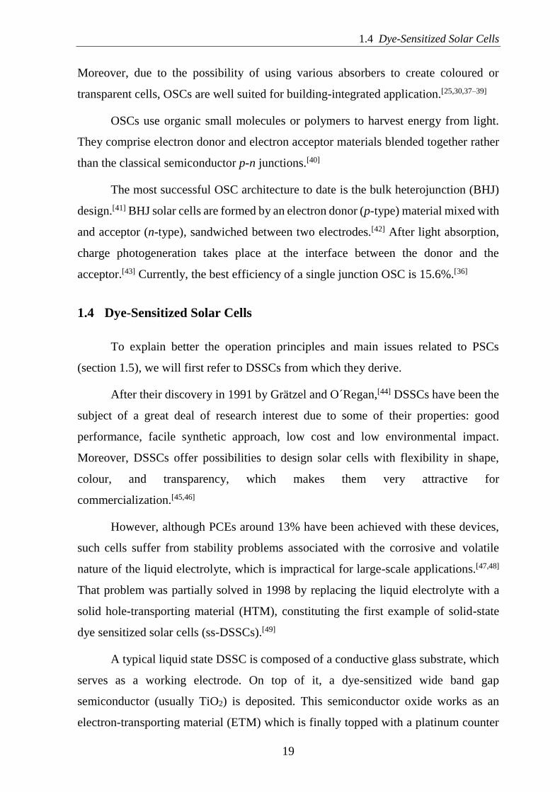
1.4 Dye-Sensitized Solar Cells
To explain better the operation principles and main issues related to PSCs
(section 1.5), we will first refer to DSSCs from which they derive.
After their discovery in 1991 by Grätzel and O´Regan,[44] DSSCs have been the
subject of a great deal of research interest due to some of their properties: good
performance, facile synthetic approach, low cost and low environmental impact.
Moreover, DSSCs offer possibilities to design solar cells with flexibility in shape,
colour, and transparency, which makes them very attractive for
commercialization.[45,46]
However, although PCEs around 13% have been achieved with these devices,
such cells suffer from stability problems associated with the corrosive and volatile
nature of the liquid electrolyte, which is impractical for large-scale applications.[47,48]
That problem was partially solved in 1998 by replacing the liquid electrolyte with a
solid hole-transporting material (HTM), constituting the first example of solid-state
dye sensitized solar cells (ss-DSSCs).[49]
A typical liquid state DSSC is composed of a conductive glass substrate, which
serves as a working electrode. On top of it, a dye-sensitized wide band gap
semiconductor (usually TiO2) is deposited. This semiconductor oxide works as an
electron-transporting material (ETM) which is finally topped with a platinum counter

1 Introduction
20
electrode. Ultimately, the system is filled with an electrolyte (typically I-/I3- ), which
serves as HTM (Figure 14).[47]
Figure 14. Schematic representation of a liquid state DSSC illustrating the basics underlying device
operation.
Compared to all solar cells above-mentioned, in which the semiconductor
assumes the task of light absorption and charge carrier transport, in DSSCs the two
functions are separated.[50] When sunlight strikes in a DSSC, light is absorbed by the
dye, exciting it from the ground state (Dye) to an excited state (Dye*), meaning that an
electron from the dye is excited from HOMO to LUMO (Equation 3):
Dye + hν →Dye* (3)
The excited electrons are then injected into the CB of the TiO2, resulting in the
oxidation of the dye (Dye+). Injected electrons travel between TiO2 nanoparticles
toward the working electrode (Equation 4):
Dye*→ Dye+ + e- (TiO2) (4)
The oxidized dye (Dye+) is regenerated by the electrolyte, which prevents back
transfer of the photogenerated electron or degradation of the dye (Equation 5):
2Dye++ 3I- → 2Dye + I3- (5)

1.5 Perovskite Solar Cells
21
Finally, the tri-iodide ions reduce back to iodide (regeneration), when they
diffuse towards the counter electrode, by the electrons that return from the external
load (Equation 6):[24]
I3- + 2e-
Pt→ 3I- (6)
1.5 Perovskite Solar Cells
1.5.1 Historical Development of Perovskite Solar Cells
In 2009, Miyasaka and co-workers used for the first time a perovskite as active
light absorber instead of using the typical molecular dye in a DSSC. They showed a
PCE of 3.1% when using the CH3NH3PbBr3 perovskite and 3.8% when using the
CH3NH3PbI3 perovskite.[51] Then, in 2011, Park and co-workers reported the use of
CH3NH3PbI3 nanocrystals or quantum dots as sensitizer reaching a PCE of 6.5%.
However, although the efficiency was improved these solar cells suffered from lack of
long-term stability, because the perovskite gradually dissolved into the redox
electrolyte, and the device showed a significant decrease in efficiency already in the
first 10 minutes.[52]
The stability issues caused by the liquid electrolyte were overcome in 2012,
when it was replaced by the solid HTM 2,2’,7,7’-tetrakis(N,N-di-p-
methoxyphenylamine)-9-9’-spirobifluorene (spiro-OMeTAD).[53] In this work, a solar
cell was fabricated using CH3NH3PbI3 perovskite nanocrystals as light harvesters
deposited onto mesoscopic TiO2 and using the HTM spiro-OMeTAD. Not only an
efficiency of 9.7% was reached, but also devices remained stable after 500 hours.
Since this first report on a long-term durable solar cell, a great effort was devoted
to the development of this new emerging photovoltaic technology, namely perovskite
solar cells (PSCs). With further progress in device design and fabrication methods,
efficiencies have progressively increased until reaching a PCE as high as 24.2%, which
is already comparable to silicon-based technologies.[36]

1 Introduction
22
Being a new technology, the progress of PSCs is unprecedented. Over 10 years
of development PSCs got an efficiency of 24.2% (Figure 15), while for example GaAs
solar cells have reached around 29% efficiency after more than 60 years, having started
at 4% in 1956.[36,54] In fact, PSCs were recognized as one of the biggest scientific
breakthroughs of 2013.[55]
Figure 15. Efficiency evolution of perovskite solar cells.
These results illustrate the potential of PSCs and the possibility to achieve even
higher efficiencies, and in that way to meet the energy needs of modern society by
making a major impact in generating inexpensive and sustainable electricity.
1.5.2 Hybrid Organic-Inorganic Perovskite Materials
Structure
Perovskites are a class of crystalline materials with the general formula ABX3
that exhibit a crystal structure similar to that of CaTiO3. Specifically, they form a three-
dimensional cubic structure based on corner sharing BX6 octahedra, in which the X-
anions are located at the corners, the smaller B cation is in the middle of the octahedra
while the larger A cation occupies interstitial space created by eight adjacent octahedral
2008 2010 2012 2014 2016 2018 20200
5
10
15
20
2521.6% May 2019.
NREL, efficient chart
24.2%
Science, 2017, 356, 1367-1379.
22.1% (FAPbI3/MAPbBr
3)
Nat. Energy, 2016, 1, 16142.
((FAI)0.81
(PbI2)
0.85(MAPbBr
3)
0.15)
Science, 2015, 348, 1234-1237.
20.2% ((FAPbI3)
1-x(MAPbBr
3)
x)
Science, 2014, 345, 542-546.
19.3% (MAPbI3-x
Clx)
Nature, 2013, 501, 395-398.
15.4% (MAPbI3-x
Clx)
Science, 2012, 338, 643-647.
10.9% (MAPbI2Cl)
Nanoscale, 2011, 3, 4088-4093.
6.5% (MAPbI3)
J.Am.Chem.Soc., 2009, 131, 6050-6051.
Eff
icie
nc
y (
%)
Year
3.8% (MAPbI3)

1.5 Perovskite Solar Cells
23
(Figure 16).[56] In the case of hybrid organic-inorganic perovskites (referred to as halide
perovskites) A is a monovalent organic cation, B is a divalent metal and X is a
monovalent halide anion.
Figure 16. Cubic perovskite crystal structure (unit cell).
To predict the stability and distortion of the perovskite structure after the
combination of the constituents A, B and X, the Goldschmidt tolerance factor (t) and
the octahedral factor (µ) are used (Equations 7-8):
t = rA+ rX
√2 (rB+ rX) (7)
μ = rB
rX
(8)
Where rA, rB and rX are the ionic radii of A, B and X, respectively. Typical halide
perovskites are stable when they have a tolerance factor in the range 0.81-1.11 and an
octahedral factor in the range 0.44-0.90.[57] For instance, a [0.89-1.0] tolerance factor
indicates a cubic structure of the perovskite, while a value lower than 0.89 indicates
less symmetry, such as tetragonal or orthorhombic structure.[58,59]
The Goldschmidt tolerance factor dictates whether a stable perovskite crystal
structure can form or not. In this respect, small cations on the A site, typically
methylammonium (MA or CH3NH3+), formamidinium (FA or (NH2)2CH+), Cs+ and/or,
Rb+ can form perovskites with halide X anions such as chlorine (Cl-), bromine (Br-),

1 Introduction
24
and/or iodine (I-). Finally, the structure is completed with the divalent metal cation (B)
such as tin (Sn2+), copper (Cu2+) and/or lead (Pb2+).[60–62]
Properties
Since the first use of perovskite materials in solar cells, they have attracted great
attention because of their excellent semiconductor properties ideally suited to
photovoltaics:[62]
- Broad range of solar absorption extending over visible or near-infrared
region.
- Strong optical absorption. The absorption coefficient of perovskites is high
across a wide wavelength range.[63] For instance, the absorption coefficient of the most
common perovskite used in PSCs (CH3NH3PbI3) is 1.5 x 104 cm-1 at 550 nm, which is
one order of magnitude higher than that of the most typical dye used in DSSCs.[55,64,65]
This large absorption coefficient guarantees efficient light-harvesting and generation
of high density of photoexcited charges which enables the use of a small thickness
perovskite layers.[66,67]
- Tunable band gap. By varying the A, B and X content of the precursor solution,
the band gap of the perovskites can change from 1.1 to 2.3 eV.[65] In this way, it is
possible to optimize light absorption tuning the composition in a controlled manner and
as result, maximize the performance of the device.[57]
Figure 17 shows how the band gap changes by modifying the composition of
the perovskite.[65]
Figure 17. Band gaps of different perovskite materials.

1.5 Perovskite Solar Cells
25
- Ambipolar charge-transport capabilities. Perovskite materials not only act as
light absorbers, but also as charge transporters of both electrons and holes, which can
simplify the device structure.
- Long electron and hole diffusion lengths of 100 nm for CH3NH3PbI3.[68] After
electron-hole pair generation, the charges have to be able to reach their corresponding
electrodes before recombining in order to generate current. The diffusion length is
defined as the average distance that a charge carrier can do before recombining.
Therefore, the higher diffusion length, the lower charge recombination and
consequently, more charge carriers will get to the electrodes.
- High charge carrier mobility, which are in the range of 5-10 cm2 V-1 s-1 for
holes and 2-10 cm2 V-1 s-1 for electrons.[69]
- Low-binding energy. It is still a matter of debate whether excitons or free
charges are created after light absorption.[70] This is an important issue, which affect
the operation of photovoltaic cells because the resulting exciton has an associate
binding energy that needs to be overcome, for electrons and holes to contribute to the
photocurrent. Recently, it has been demonstrated the formation of both excitons and
free charges after photoexcitation of CH3NH3PbI3.[71,72] But even if excitons are
created, there are various studies indicating low lifetimes since the binding energy of
those are in the range of a few electronvolts.[71–74]
All the aforementioned properties together with the fact that these inexpensive
materials can be processed employing several techniques (including solution
processing) makes them compatible with low-cost and large-scale roll-to-roll
fabrication techniques.[75]
1.5.3 Working Principle and Device Structures
A typical PSC consists of a thin film light-harvesting perovskite layer
sandwiched between an electron-transporting layer (ETL) and a hole-transporting layer
(HTL) together with two electrodes. If sunlight enters through the ETL (n-side),
electrons are collected at the bottom of the device and this structure is called n-i-p or
regular structure. On the contrary, if the light goes through the HTL, so the holes are

1 Introduction
26
collected at the bottom of de device, the structure is called p-i-n or inverted. The regular
architecture can be classified into mesoscopic, in which a mesoporous oxide is used,
or planar structure.[76,77]
Most of the PSC world record efficiencies were achieved with the regular
mesoscopic architecture (Figure 18C), since devices with this architecture showed
insignificant hysteresis (see section 1.6.3 for problems related to hysteresis).
A) Regular structured PSC B) Inverted structured PSC
C) Regular mesoscopic PSC D) Regular planar PSC E) Inverted PSC
Figure 18. Energy level alignment of typical (A) regular and (B) inverted PSC and main processes:
Absorption of photon and free charges generation (1), charge transport (2) and charge extraction (3).
Examples of device structures of (C) regular mesoscopic, (D) regular planar and (E) inverted PSC.
In a mesoscospic structure a glass substrate coated with a fluorine-doped tin
oxide (FTO) layer, which serves as an electrode, is covered by a compact hole blocking
layer (normally TiO2). The compact TiO2 (c-TiO2) plays an important role, suppressing
charge recombination at the interface by preventing direct contact between the FTO
and the ETM. On top of the compact layer, a mesoporous oxide is layered. If the metal
E
FTO Metal
VB
HTM
LUMO
ETM
hν
e-
e- h+
h+
h+
e-
e-
HOMO
Perovskite
1
2
2
3
3
E
ITO Metal
VB
HTM
LUMO
ETM
hν
e-
e-
h+
h+
h+
e-
e-
HOMO
Perovskite
1
2
2
3
3

1.5 Perovskite Solar Cells
27
oxide is a semiconductor (TiO2 typically, SnO2, ZnO), this layer acts as an active
scaffold, since it takes electrons from the perovskite layer and transport them to the
electrode. When replacing the mesoporous semiconductor oxide by an insulator (Al2O3
typically, ZrO2), the scaffold is passive, since it cannot transport charges and electron
transport occurs inside the perovskite. After the mesoporous layer, the perovskite is
deposited, penetrating through the pores of the oxide, and then covered with the HTM,
usually spiro-OMeTAD or poly [bis(4-phenyl)(2,4,6-trimethyl)amine] (PTAA).
Finally, the system is completed by the deposition of a metal electrode (usually gold)
on top of the HTM.[76,78,79]
In the regular planar structure, the architecture is similar to the regular
mesoscopic structure above described, but the mesoporous layer is skipped (Figure
18D).
The working principle of a PSC with a regular architecture is as follows (Figure
18A): Once illuminated by sunlight, the perovskite absorbs photons with energy equal
to or greater than its band gap generating free electrons and holes. After excitation,
electrons will be injected from the perovskite to the ETM at the ETL/perovskite
interface, then transported through the ETM and finally collected by the FTO electrode.
Correspondingly, holes will be extracted at the perovskite/HTL interface; transported
across the HTM and collected to the back gold electrode.[25]
In the inverted or p-i-n structure, commonly indium tin oxide (ITO) is used as
the hole-collecting bottom electrode, covered by the HTM [usually poly (3,4-
ethylenedioxythiophene):polystyrene sulfonate (PEDOT:PSS) or NiOx] and followed
by the deposition of the perovskite absorber. Subsequently, an ETM, typically [6,6]-
phenyl-C61-butyric acid methyl ester (PCBM), is deposited and finally an aluminium
or silver top electrode is used as the electron-collecting unit completing the device
(Figure 18E). With this configuration the working principle is similar to the above
described for the regular one, but for the places where the electrons and holes are
collected (Figure 18B).[76,77]

1 Introduction
28
1.6 Obstacles towards Large-Scale Application of PSCs
Despite the high efficiency and relatively low cost of the materials used in PSCs,
there are several issues which have to be resolved in order to promote PSCs a feasible
photovoltaic technology. These include long-term stability, toxicity, hysteresis and
scale up of the cell area.[80]
1.6.1 Long-Term Stability
Long-term stability remains a major challenge toward large-scale application of
PSCs since they suffer from high sensitivity to environmental factors like moisture,
oxygen, ultraviolet (UV) light or high temperatures, among others.[81–86] As a matter of
fact, to commercialize PSCs it is necessary that the devices can operate continuously
for about 25 years in outdoor conditions.[87]
Oxygen and UV light
The instability of PSCs against UV radiation is primarily due to the widely
employed mesoporous TiO2 (m-TiO2). PSCs show a decrease in efficiency after UV
light exposure mainly because of the presence of surface defects in the TiO2 structure.
Moreover, the reaction between TiO2 and the perovskite layer can lead to further drops
in the efficiency.
TiO2 contains many surface defects, most of them oxygen vacancies, which can
be understood as unpaired electrons. These extra electrons can react with oxygen from
the ambient air and lead to the formation of an anion radical (O2- ). Upon UV excitation,
an e-/h+ pair is created in the bulk of the TiO2 structure and the h+ migrates to the surface
of the TiO2. In that place, the h+ recombines with the anion radical previously formed
converting it into O2, which gets desorbed from the TiO2 surface, leaving a space (trap).
If a PSC is illuminated, the perovskite will absorb photons and will create an e-/h+ pair.
The electron could stay in one of these trap states and recombines with holes instead
of travelling to the electrode and producing current, which would end up in a loss of
efficiency.[88]

1.6 Obstacles towards Large-Scale Application of PSCs
29
In addition, instability caused by UV in PSCs can partly arise from an interaction
at the TiO2/perovskite interface. The degradation mechanism of the perovskite layer
could be understood taking into account the possible reactions at the TiO2 surface
(Equations 9-11):[89]
2I-↔ I2 + 2e- (9)
3CH3NH3+ ↔ 3CH3NH2↑ + 3H+ (10)
I- + I2 + 3H++ 2e-↔ 3HI↑ (11)
First, TiO2 extracts an electron from I- in the CH3NH3PbI3 crystal structure
forming I2 at the TiO2/CH3NH3PbI3 interface (Equation 9). That electron may return to
the TiO2 surface giving rise to the formation of HI (Equation 11). As H+ is consumed
(Equation 11), the equilibrium of equation 10 shifts to the right side, which results in
the progressive degradation of the perovskite.
To overcome the UV-instability problem, pacifying electronic trap states, use of
ultraviolet cut-off filters or replacing the mesoporous TiO2 with other materials have
been proposed.[90,91]
High temperature
Another factor that affects the PSC performance is temperature. This is an
important issue to be addressed because an annealing process for crystallization after
deposition of the perovskite is necessary, and depending on the temperature at which
the process is carried out a difference morphology, composition and as a result, device
performance will be achieved.[92] Moreover, solar modules will be exposed under
standard operating conditions, so thermal stability is a key aspect that determines the
efficiency of the device.
The thermal degradation of perovskite devices depends on several factors, such
as the intrinsic temperature degradation of the perovskite, electrodes or charge
transporting layers.[93] It has been demonstrated that CH3NH3PbI3 suffers degradation
when it is heated up to 100 ºC for a short period of time.[85,94]

1 Introduction
30
Thus, perovskite not only undergoes rapid decomposition resulting in a decline
in device performance, but one of the decomposition products, PbI2, is water-soluble
and it could lead to environmental problems due to its toxicity.
Moreover, perovskite materials suffer reversible phase transitions as a function
of the temperature. For example, CH3NH3PbI3 was shown to have three structural
phases: a cubic phase above 330 K, a tetragonal phase from 160 to 330 K, and an
orthorhombic phase below 160 K.[95] It has been shown a drop in photovoltaic
performance at around 55 ºC corresponding to the transition between a tetragonal phase
of CH3NH3PbI3 to the cubic phase.[96,97]
One of the proposed strategies to improve the thermal stability of PSCs is the
modification of the perovskite layer by adding additives. In this regard, Tress and co-
workers employed carbon nanoparticles as additives to control the morphology of the
perovskite film.[98] They demonstrated that perovskite films containing carbon
nanoparticles as additives presented higher thermal stability than films without them.
Moisture
PSCs are also susceptible to moisture, which is one of the major factors of
degradation. The perovskite hydrolyses in the presence of moisture producing the two
precursors (Equation 12):
CH3NH3PbI3 (s) ↔ PbI2 (s) + CH3NH3I (aq) (12)
Then, CH3NH3I decomposes to produce HI (Equation 13), which afterwards can
react in the presence of oxygen (Equation 14), or after the exposition to UV light
(Equation15).
CH3NH3I (aq) ↔ CH3NH2 (aq) + HI (aq) (13)
4HI (aq) + O2 (g) ↔ 2I2(s) + 2H2O (l) (14)
2HI (aq) + hν ↔ H2(g) + I2 (s) (15)
Therefore, the preparation of PSCs should be conducted inside a glove box filled
with an inert gas (normally nitrogen).[91]

1.6 Obstacles towards Large-Scale Application of PSCs
31
1.6.2 Toxicity of Lead
An important issue of PSCs is the toxicity of lead, a component in the perovskite
material, which is employed in most PSCs exhibiting good performance. This fact has
opened up a new research field in order to solve this issue and to further explore non-
or low-toxic perovskite materials.[99]
Actually, PSCs cannot be commercialized in the European Union because there
is a strict directive. This regulation restricts to 0.1% in weight the maximum
concentration of lead in each homogenous material contained in any electronic device.
Unfortunately, all the halide perovskites that have been so far demonstrated as effective
photovoltaic materials contain more than 10% lead in weight and indeed they are
banned from the European energy market.[100]
In this context, recent research has focused on the replacement of Pb2+ with other
suitable cations in perovskites.[101] As an example, germanium (II) (Ge2+),[102] tin (II)
(Sn2+)[103] or mixed Sn-Ge[104] were used as a substitute of Pb2+ in PSCs. However, the
resulted perovskite materials exhibited low stabilities, because those cations tend to
oxidize, from Sn2+ to Sn4+ or Ge2+ to Ge4+, leading to vacancies that induced
instability.[105]
1.6.3 Hysteresis
The hysteresis is a phenomenon occurring in PSCs whereby there are changes
in the response of the device depending on the direction and rate of the applied voltage.
In other words, a different J-V curve is obtained depending on whether a backward
(from positive to negative voltage) or forward (from negative to positive voltage) scan
is applied (Figure 19).[106]
Although the origin of hysteresis is still unclear, different mechanisms have
been proposed that could rationalize the experimental findings. These include
ferroelectric polarization, ion migration, charge trapping and capacitive effects.[107]
The hysteresis phenomenon hinders the proper characterization of PSCs because
it prevents the accurate determination of the efficiency.

1 Introduction
32
Figure 19. J-V hysteresis in regular (left) and inverted (right) PSCs. Discrepancy between the J-V
curve when scanned from positive to negative voltage (black) and from negative to positive (red).[25]
1.6.4 Scale up
Transition from laboratory-scale fabrication to industrial manufacturing
requires scaling up. However, there are some issues to address since the reported record
efficiencies for PSCs generally come from devices with a very small active area and it
is expected that efficiency drops when scaling up. In fact, it has been already
demonstrated that increasing the cell dimension from 0.12 cm2 to 1.10 cm2 results in a
PCE drop from 17.5% to 15.5%.[108]
There have been already reported photovoltaic panels based on PSCs. Fan and
co-workers reported an efficiency of 10.6% for modules of 17.3 cm2 of active area
based on FTO/ZnO/active layer/carbon cells structure without degradation after 140
days of outdoor testing.[109] The same group has fabricated a perovskite module of 45
x 65 cm2 using the same approach (Figure 20, left). Also, Han and co-workers
demonstrated stable and 10.4% efficient 10 x 10 cm2 perovskite modules, with an
active area of 49 cm2, using a 10 HTM free-based PSC with an FTO/c-TiO2/m-TiO2/m-
ZrO2/m-C/perovskite architecture.[110] 96 of those modules constituted a 1 m2 panel,
that together with 6 panels more, formed the photovoltaic panel that is shown in Figure
20 (right).
Apparently, for large-scale devices efficiency falls far behind the record values
reported for small area lab devices. In addition, an important step towards the
fabrication of large-area modules is the development of new deposition methods

1.6 Obstacles towards Large-Scale Application of PSCs
33
suitable for industrial production that can provide high-layer uniformity with large
crystals and fewer grain boundaries over the large area.
Figure 20. Left: Power plant composed of 32 modules with an area of 45 x 65 cm2 connected in
between.[109]. Right: 7 m2 printable perovskite-based panels.[110]
The progress in PSCs has been tremendous so far, reaching up high efficiencies
in a short period, and becoming a promising candidate in the photovoltaic field.
However, as mentioned above, there are still several issues that should be addressed
for further development of PSCs in order to be taken out of the lab for practical
application. Optimizing the perovskite material, deposition techniques or device
architectures as well as looking for different hole- and electron-transporting materials
will be instrumental to overcome those issues.


2. DOPANT-FREE HOLE-
TRANSPORTING POLYMERS FOR
PEROVSKITE SOLAR CELLS


2.1 Introduction
37
2 DOPANT-FREE HOLE-TRANSPORTING POLYMERS FOR
PEROVSKITE SOLAR CELLS
2.1 Introduction
Over the past ten years, we have witnessed the rise of PSCs, one of the most
impressive evolutions in the history of photovoltaics. PSCs have gained considerable
research attention and have emerged as an extremely promising photovoltaic
technology due to their remarkable photovoltaic performance and potentially low-
production cost. However, this exceptional fast growth is not yet enough to guarantee
a spot in the market of solar cells, which is still lead by silicon solar cells.
Among the serious challenges to be addressed, stability remains as one of the
biggest issues to be resolved. Significant research efforts in different areas were
devoted in attempts to fabricate not only efficient but also long-term stable PSCs. In
this effort, among others, HTMs have been intensively studied with the objective of
increasing the efficiency and improving the stability of the perovskite-based devices.
This chapter focuses on the role of different materials used as HTMs in
influencing long-term stability, improving the photovoltaic parameters and thereby
enhancing the efficiency of PSCs.
2.1.1 Role and Properties of Hole-Transporting Materials in PSCs
It has been shown in section 1.5.3 that the photovoltaic process in PSCs takes
place in three steps, namely (1) absorption of sunlight and formation of free charges,
(2) charge transport and (3) collection of charges at the electrodes (Figure 21). Toward
the two latter processes, the HTM plays a crucial role in PSCs, ensuring an efficient
hole extraction at the perovskite/HTM interface and improving hole transport from the
perovskite to the electrode. Although perovskite materials can conduct holes, the use
of HTMs remains indispensable in almost all the architectures utilized in PSCs.[111]
Unfortunately, during device operation, undesirable charge-transfer processes
can take place in PSCs (dashed lines in Figure 21). In this context, apart from extracting

2 Dopant-Free Hole-Transporting Polymers for Perovskite Solar Cells
38
holes and transporting them to the electrode, the HTM helps to avoid these troublesome
mechanisms, which affect prejudicially the solar cell performance.[112] For instance, if
the HTM is correctly chosen, it can act as electron-blocking layer to prevent the
recombination losses or back-transfer processes at the perovskite/HTM interface
leading to improved device performance.[77] Moreover, the presence of the HTM avoids
the direct contact of the metal electrode with the perovskite layer, which also minimizes
charge recombination.[113] Furthermore, in many PSCs the HTM constitutes the first
line of defence against external agents, so it plays an important role in the device
performance as well as in the stability of PSCs.[114]
Figure 21. Schematic representation of electronic processes in PSCs. Adapted from reference [112].
For efficient PSCs an ideal HTM should fulfil several general requirements: (i)
The HOMO energy level of the HTM should be higher than the VB energy of the
perovskite in order to ensure an efficient extraction of the holes from the perovskite to
the HTM, minimizing injection losses. Moreover, the HOMO level of the HTM
influences the VOC, which consequently affects the PCE of the device.[115] (ii)
Furthermore, the HTM should have reasonable hole mobility and conductivity in order
to allow rapid transport of the photogenerated holes to the back contact electrode
(counter electrode) and prevent charge recombination.[114,116] Neverhteless, HTMs with
low conductivity can be doped in order to enhance it, although the presence of dopant
additives has been linked to long-term degradation. In an ideal situation, dopant-free
HTMs will be paramount for the successful operation of PSCs. (iii) They must be
thermal and photochemically stable and resistant to external degradation factors.[117]
(iv) They should have enough solubility and good film-forming ability for processing
VB h+
CB e-
HOMO
LUMO
Perovskite
HTM
ETM
hν
E(e
V)
ElectrodeElectrode
e-
h+
(1)
(2)
(2)
(3)
(3)

2.1 Introduction
39
and device fabrication.[118,119] (v) Amorphous HTMs with appropriate glass transition
temperature (Tg), usually above 100 ºC, are desirable.[120] Taking into account that
devices operate at higher temperatures than room temperature, sustaining the
amorphous state is important. (vi) They should be cheap and environmental-friendly.
(vii) An ideal HTM should not absorb in the visible region for not competing with the
perovskite in the absorption of light. A good strategy has proven to be using HTMs that
absorb in regions where the perovskite has a weaker absorption. Since the most
efficient perovskites have a band gap around 1.5 eV (onset at 820 nm), HTMs with
lower band gaps would offer the possibility to absorb additional photons at longer
wavelengths and consequently, the PCE of the solar cell would be improved.[117]
2.1.2 Hole-Transporting Materials for PSCs
Spiro-Structured Hole-Transporting Materials
Spiro-OMeTAD has been the most commonly used standard and is still the
predominant HTM employed in the majority of PSCs (Figure 22, left).[116]
Figure 22. Molecular structures of spiro-OMeTAD (left) and TPD (right).
It could be intuited from its name that spiro-OMeTAD is based on the spiro
structure, in which two extended π-systems are connected to a sp3-hybridized atom.
The perpendicular arrangement achieved with this configuration lends spiro-based
molecules to a rigid structure, which give them high morphological stability, whereas
the electronic properties of the electroactive moieties remain intact.[120]
Spiro-OMeTAD was first synthesized in 1997 by Salbeck and co-workers[121] as
an alternative material to TPD [N,N′-diphenyl-N,N′-bis-(3-methylphenyl)-N,N′-

2 Dopant-Free Hole-Transporting Polymers for Perovskite Solar Cells
40
bis(phenyl)benzidine], which has been widely used as HTM in organic light-emitting
diodes (OLEDs) (Figure 22, right). TPD suffers from low morphological stability of
the amorphous state, due to its low Tg (62 ºC). In contrast, spiro-OMeTAD shows
improved thermal stability (Tg = 124 ºC) compared to TPD without compromising its
electronic properties.[122]
The incorporation of eight electron donating p-methoxy groups leads to an
HOMO energy level of -5.22 eV, which is well-aligned with the VB of the most
common perovskites used in PSCs. Moreover, spiro-OMeTAD is colorless (Eg = 2.95
eV) and consequently, it does not compete with the perovskite for light absorption.[123]
In addition to the good optoelectronic properties and appropriate glass-forming
properties, it exhibits good solubility in common organic solvents, which is very
important for good film formation and processing.[124] Nevertheless, spiro-OMeTAD
is far from being the perfect HTM for different reasons. The drawbacks of spiro-
OMeTAD are its synthetic complexity, high synthetic cost and the requirement of
dopants to improve its hole-transport behavior and device performance. Furthermore,
high temperatures are detrimental for this molecule, which crystallizes at 182 ºC losing
its efficiency as HTM.[125,126]
Regarding the use of dopants, spiro-OMeTAD itself has low conductivity (~10-
5 S cm-1) and hole mobility (~10-6-10-5 cm2 V-1 s-1) and to reach the best performances
the use of additives is a prerequisite. For spiro-OMeTAD, the widely employed
dopants are lithium bis[(trifluoromethyl)sulfonyl]amide (Li-TFSI), 4-tert-
butylpyridine (tBP), and a series of organic cobalt salts such as tris[2-(1H-pyrazol-1-
yl) pyridine)] cobalt (III) tris(hexafluorophosphate) (FK102) and tris[2-(1H-pyrazol-1-
yl)-4-tert-butylpyridine]-cobalt(III)-tris[bis(tri-fluoromethylsulfonyl)imide] (FK209).
Those dopants act introducing additional holes, which leads to an increased
charge carrier density in the doped molecule. This process results in a higher
conductivity, according to equation 16, where σ is the conductivity, e the elementary
charge and nx y μx are the density and mobility of the positive (p) and negative (n)
charge carriers, respectively.[127]

2.1 Introduction
41
σ = σn + σp = (nneμn) + (npeμ
p) (16)
However, the presence of dopants has been related to the reduction of the long-
term stability, due to their migration throughout the perovskite layer.[128,129] To
overcome these disadvantages, many research groups are working on replacing spiro-
OMeTAD with alternative HTMs that yield PSC devices with high efficiency and
stability. As a result, a number of organic small molecules, conducting polymers,
organometallic complexes, and inorganic semiconductors have been reported as HTMs
for high performing PSCs.[93,111,112,114,116,118,130] Among them, conjugated polymers
have attracted great attention due to their thermal and mechanical stability, tunability
via molecular design and synthesis, or the wide variety of choice.[131] Moreover,
compared to small molecules, polymers own higher hole mobility and superior film-
forming properties.[132]
If we have a look at the conjugated polymers that have been used as HTMs in
PSCs, it is evident that most of them were previously used in OSCs as p-type materials.
However, there are some polymers that have been specifically designed as HTMs for
PSCs.
In the following section, we will comment some of the most representative
examples of polymers that have been used as HTMs in PSCs in recent years.
Hole-Transporting Polymers for PSCs
In Figure 23 is displayed some of the most representative examples of hole-
transporting polymers for PSCs.
PTAA (HTM-1) is a polymeric structure of triphenylamines, which was the first
polymer tested in PSCs. PTAA exhibits high hole mobility (10-2-10-3 cm2 V-1 s-1)
compared with other polymers and a suitable HOMO, which determines its excellent
hole-extraction and electron-blocking properties.[114] The group of Seok achieved an
impressive 22.1% in efficiency using PTAA as HTM, which is the record efficiency in
PSCs for a polymeric HTM.[133] In that work, they demonstrated that the introduction
of additional iodide ions in the perovskite layer increased the VOC and JSC, by
decreasing the concentration of deep-level defects.

2 Dopant-Free Hole-Transporting Polymers for Perovskite Solar Cells
42
An oligomer derivative from PTAA (S197, HTM-2) was obtained by Grätzel,
Nazeeruddin, and co-workers. Its backbone consists of approximately 9 units that carry
an additional o,p-dimethoxyphenylene substituent comparing to PTAA. It was found
that devices using S197 as HTM in a mesoscopic regular architecture reached a 12.0%
in efficiency, which was higher than those devices using PTAA as HTM under the
same conditions.[134]
Figure 23. Structure of some polymeric HTMs used in PSCs.
PEDOT:PSS (HTM-3) is a polymer electrolyte consisting of positively charged
conjugated PEDOT and negatively charged PSS. PEDOT is usually doped with PSS,
which is a polymeric surfactant, which helps to disperse and stabilize PEDOT in
solvents.[135] PEDOT:PSS is a commercial low-cost polymer that has been mostly
employed as HTM in inverted PSCs. It exhibits an HOMO level compatible with the

2.1 Introduction
43
VB of perovskites and also compatible with the work function of the ITO, which
enables hole extraction and transport. Moreover, this polymer has excellent film
properties and the low temperature necessary for the annealing process makes it
compatible with flexible electronic devices.[93,112] The highest efficiency using
PEDOT:PSS as HTM in PSCs was reported by Im and co-workers.[136] In that work, an
efficiency of 18.1% was achieved with ITO/PEDOT:PSS/CH3NH3PbI3/PCBM/Au
inverted architecture using HI as additive to ensure a very high quality perovskite film.
However, PEDOT:PSS is sensitive to humidity due to its hygroscopic nature, which
affects the stability of PSCs.
In addition, the use of thiophene-based polymers, which have been used in the
field of OSCs as electron donors, have been also investigated as HTMs in PSCs. Poly
(3-hexylthiophene-2,5-diyl) (P3HT, HTM-4) has been one of the most widely used
polymers among this family in PSCs.[137–139] It shows suitable optical and electrical
properties, good thermal and chemical stability as well as high processability, but
efficiencies remain lower than those using spiro-OMeTAD or PTAA. Lately, P3HT
was used as HTM in a PSC using a regular mesoporous architecture and a 17.8% in
efficiency was reached.[140]
Furthermore, donor-acceptor polymers with low-band gap have been also tested
as HTMs in PSCs. Recently, Lidzey and co-workers[141] have reported the use of
poly[N-9’-heptadecanyl-2,7-carbazole-alt-5,5-(4’,7’-di-2-thienyl-2’,1’,3’-
benzothiadiazole)] (PCDTBT, HTM-5) as HTM in a PSC reaching an efficiency of
almost 16%, which was highly comparable with reference devices using spiro-
OMeTAD. Also, in a work by Sun and co-workers [142] a PCE of 15.1% was achieved
when poly{2,6-[4,4-bis-(2-ethylhexyl)-4H-cyclopenta[2,1-b;3,4-b’]dithiophene]-alt-
4,7(2,1,3-benzothiadiazole)} (PCPDTBT, HTM-6) was incorporated as HTM in PSCs.
With further modifications, diketopyrrolopyrrole-based polymers, poly[N-90-
heptadecanyl-2,7carbazole-alt-3,6-bis(thiophen-5-yl)-2,5-dioctyl-2,5-
dihydropyrrolo[3,4] pyrrole-1,4-dione] (PCBTDPP, HTM-7)[143] and poly[2,5-bis(2-
decyldodecyl) pyrrolo[3,4-c]pyrrole-1,4(2H,5H)-dione-(E)-1,2-di(2,2’-bithiophen-5-
yl)ethene], (PDPPDBTE, HTM-8)[144] were also tested in PSCs, resulting in PCEs of
5.6% and 9.2%, respectively.

2 Dopant-Free Hole-Transporting Polymers for Perovskite Solar Cells
44
Other polymers based on benzodithiophene derivatives (i.e., HTM-9, HTM-
10)[145] or polymers containing fluorene derivatives (i.e., HTM-11, HTM-12, or HTM-
13)[146] have also been applied as HTMs in perovskite-based solar cells showing
significant solar-cell performances.
The best performances obtained with many of the above-mentioned
investigations (except from HTM-9 and HTM-10), were achieved by doping the HTM
solution with additives. As it was mentioned before, these dopants help to enhance the
performances of the HTM with mechanisms that are not yet completely clear, even if
it is supposed that they have effects on the conductivity of the layer. However, they are
deliquescent and hygroscopic; they degrade the perovskite film as well as the organic
HTL, diminishing the stability of the device and leading to important losses in
performance.[122,147] For example, dopant LiTFSI is added to the HTM solution
dissolved in CH3CN, which is known to attack the perovskite and therefore, even if it
is added in a very small amount, it could partially degrade the perovskite layer.
Moreover, doping increases the overall cost and requires a strict optimization of the
doping conditions.
For these reasons, the next generation of HTMs should have not only appropriate
properties, but also they have to be able to work in the absence of dopants (so-called
dopant-free HTMs). In that way, removing additives has become an important
objective for long-term stability of PSCs.
2.1.3 Efficient Dopant-Free Hole-Transporting Polymers for PSCs
Working without dopants was already shown to be a feasible strategy for
efficient and stable PSCs. Some small molecules have been tested recently as HTMs
in PSCs in the absence of dopants and not only have they reached efficiencies
comparable to that of devices using doped spiro-OMeTAD, but also they showed an
improved stability.[148–155]
Polymers have been much less explored than small molecules even though they
offer excellent properties. In Figure 24, some examples of dopant-free polymeric
HTMs used in PSCs are shown.

2.1 Introduction
45
Figure 24. Molecular structures of dopant-free hole-transporting polymers.
Recently, Park and co-workers[147] reported a novel polymeric HTM based on
benzo[1,2-b:4,5:b´]dithiophene (BDT) and 2,1,3-benzothiadiazole (BT) units (HTM-
14), for using it in PSCs without any dopant. A PCE of 17.3% was achieved,
maintaining its initial efficiency for more than 1400 hours. The same authors have
reported the highest performance with a device fabricated with a dopant-free polymeric
HTM. In their work the polymeric HTM, consisting in a BDT unit as a donor and a BT
unit as acceptor connected with a π-bridge (HTM-15), was incorporated in PSCs
reaching an impressive PCE of 19.8%.[156]
Also, in a work by Getautis, Saliba and co-workers[157] three new triarylamine-
based polymers (HTM-16, HTM-17 and HTM-18) were tested as HTMs in the
absence of dopants leading to a PCE of 12.3% with the polymer poly[3,5-dimethyl-
N,N-diphenyl-4-(2-phenylprop-1-en-1-yl)aniline-4',4''-diyl] (HTM-18), which was
higher than that of PTAA (10.8%) measured under the same conditions. Moreover,
devices prepared with this dopant-free polymer were stable for over 140 hours without

2 Dopant-Free Hole-Transporting Polymers for Perovskite Solar Cells
46
significant changes in the PCE, while devices with the doped polymer showed a
significant decrease in efficiency already in the first few hours. Qiao and colleagues[158]
reported the well-known polymer poly{2,2'-[(2,5-bis(2-hexyldecyl)-3,6-dioxo-2,3,5,6-
tetrahydropyrrolo[3,4-c ]pyrrole-1,4-diyl)dithiophene]-5,5'-diyl-alt-thiophen-2,5-diyl}
(PDPP3T, HTM-19) as dopant-free HTM in PSCs reaching a PCE of 12.3%, which
was comparable with devices prepared with doped spiro-OMeTAD (12.34%). In
addition, PDPP3T-based PSC devices showed a better stability in ambient air than the
doped spiro-OMeTAD.
All these results verify the possibility of using polymers as dopant-free HTMs
for the development and commercialization of stable PSCs avoiding the use of any
additive.

2.2 Objectives
47
2.2 Objectives
Undoubtedly, the use of dopants to increase the conductivity of the HTM,
although beneficial for the PCE, strongly deteriorates perovskite-device stability and
decreases lifetime. Moreover, the strategy of using dopants involves more chemicals
and more cost in terms of money and time. Therefore, developing dopant-free HTMs
is essential for achieving the desired long-term stability of PSCs.
On the other hand, polymers seem to be very suitable for their incorporation as
dopant-free HTMs because of their excellent solution processability, tunable energy
levels, thin film uniformity or thermal stability.
In this sense, the main objective of this chapter is the design and synthesis of
new dopant-free HTMs for developing stable and high-efficient PSCs. In order to
achieve this purpose, the work has been divided into:
Design and synthesis of new polymeric HTMs for application in PSCs. The aim
is the preparation of a series of novel polymers derived from the combination of
different well-known accepting units, such as thiophene, triarylamine and
spirobifluorene. The characterization of the polymers will be carried out by nuclear
magnetic resonance (NMR), mass spectrometry and size exclusion chromatography
(SEC).
Characterization of the newly polymers by thermal, optical and electrochemical
techniques in order to evaluate their properties. In this regard, the newly polymers
should have optimal HOMO energy levels in order to warrant hole transport while
maintaining low visible absorption, as their function in the device is ensuring good
electronic transport from the perovskite to the electrode and not absorbing light.
Moreover, the objective polymers should have enough solubility for film formation as
well as high thermal stability.
The polymers will be incorporated as dopant-free HTMs in PSCs in order to
evaluate their device performance. Furthermore, we identified thermal stability as a
fundamental weak point of PSCs and the effect of the new dopant-free HTMs on
stability against temperature will be tested.

2 Dopant-Free Hole-Transporting Polymers for Perovskite Solar Cells
48
2.3 Results and Discussion
2.3.1 Design and Synthesis of Polymers P1-P6
The chemical structures of the target polymers P1-P6 are displayed in Figure
25. The design of the 6 new polymers was inspired by spiro-OMeTAD and PTAA,
being the latter the only polymeric HTM that could work as efficiently as spiro-type
small molecules.[159]
Figure 25. Chemical structures of the target polymers P1-P6.
Polymers P1 and P2 are composed of a spirobifluorene unit in combination with
two different donor moieties, a thiophene and a triarylamine derivative, respectively,
which are known to possess high hole-transporting and electron-blocking abilities.
Thiophenes have been intensively used as building blocks for organic semiconductors
due to their favourable optoelectronic properties. In particular, their high hole mobility
presents an attractive feature for HTM design.[111] In case of triarylamine derivatives,
because of their excellent charge-transporting properties and easy oxidizability they
have been also widely used as donor materials in several optoelectronic materials as
OLEDs, organic field-effect transistors (OFETs), DSSCs or PSCs. Especially,
polymeric triaryalmine derivatives hold great potential due to advantages such as

2.3 Results and Discussion
49
possibility of extended π-conjugation and excellent film-forming properties.[160]
Finally, the motivation to synthesize HTMs with a spiro-linked molecular fragment
was to achieve materials with high Tg, morphological stability and easy processability
while keeping good electronic properties.[122] Moreover, to ensure sufficiently high
solubility for device fabrication and good film formation, branched alkyl chains (2-
ethylhexyl) were introduced in key positions of those donor units.
In polymers P3-P6, the introduction of more donor groups in their backbone
than in polymers P1-P2 was explored in order to modulate their HOMO energy levels
for an optimized hole transport from the perovskite to the HTM. Therefore, we
designed polymers P3-P6, each one containing triphenylamine extended units in
combination with different donor systems as thiophene (P3), spirobifluorene (P4), or
triarylamine (P5) units. As in polymers P1 and P2, polymers P3-P6 will benefit from
the enhanced solubility given by the alkyl groups.
Synthesis of Functionalized Monomers
In order to prepare the target polymers, difunctionalized monomers with
bromine or boronic ester moieties were synthesized (Figure 26). Both moieties enable
the use of Pd-catalyzed Suzuki cross coupling reaction for further polymerization. In
addition, Ni-mediated Yamamoto polymerization reaction could be performed.
Figure 26. Chemical structures of monomers M1-M5 and 2,7-dibromo-9,9'-spirobifluorene.

2 Dopant-Free Hole-Transporting Polymers for Perovskite Solar Cells
50
The procedure for the synthesis of monomer M1 is shown in Scheme 1, while
the complete experimental details can be found in the experimental section. First, the
Kumada coupling of 3,4-dibromothiophene with 2-(ethylhexyl)magnesiumbromide
(RMgBr) provided thiophene 1, which after Ir-catalyzed borylation afforded monomer
M1.
Scheme 1. Synthetic route to monomer M1.
Monomer M2 was prepared according to the synthetic route outlined in Scheme
2, following literature procedures.[161–163] In this regard, the reaction between 4-
iodophenol and 2-ethylhexilbromide (RBr) in N,N-dimethylformamide (DMF) using
K2CO3 as base gave 1-(2-ethylhexyloxy)-4-iodobenzene (2) in high yield. Next,
Buchwald-Hartwig reaction of compound 2 with diphenylamine resulted in the
formation of 4-(2-ethylhexyloxy)-N,N-diphenylaniline (3), which was subjected to
react with an excess of N-bromosuccinimide (NBS), yielding triarylamine 4. Finally,
Miyaura borylation of compound 4 led monomer M2 in moderate yield.
Scheme 2. Synthetic pathway for the preparation of monomer M2.

2.3 Results and Discussion
51
The synthesis of monomer M3 started with the reaction between 1-(2-
ethylhexyloxy)-4-iodobenzene (2) and 4-bromophenylamine to give triarylamine 5.
After that, Buchwald-Hartwig reaction of compound 5 with diphenylamine gave
triarylamine 6, which finally reacted with an excess of NBS yielding monomer M3
(Scheme 3).
Scheme 3. Synthesis of di-bromine functionalized monomer M3.
The synthesis of monomer M4 was synthesized through Miyaura borylation of
the commercially available 2,7-dibromo-9,9'-spirobifluorene according to published
procedures (Scheme 4).[164]
Scheme 4. Synthesis of monomer M4.
Finally, the synthesis of monomer M5 was prepared following a three-step
synthetic procedure (Scheme 5). Firstly bis(4-bromophenyl)amine (7) was obtained by
treating diphenylamine with an excess of NBS following reported procedures.[165]
Triarylamine 8 was also synthesized by reported procedures by Cu-catalyzed Ullmann
coupling of compound 7 and 1-iodo-4-methoxybenzene.[166] Finally, monomer M5 was

2 Dopant-Free Hole-Transporting Polymers for Perovskite Solar Cells
52
obtained by Miyaura borylation of the previous synthesized triarylamine 8 in 44%
yield.
Scheme 5. Synthetic route to monomer M5.
Synthesis of Polymers P1-P6
The six new polymers P1-P6 were then synthesized recurring to either Suzuki
(P1-P5) or Yamamoto (P6) coupling polymerization.
We started with the synthesis of copolymers P1 and P2 bearing a spirobifluorene
unit in combination with two different donor moieties. The procedure for the synthesis
of both polymers is shown in Scheme 6.
Scheme 6. Synthesis of polymers P1 and P2.
P1 and P2 were synthesized by Pd-catalyzed Suzuki coupling copolymerization
of the corresponding diboronic ester monomers M1 and M2, respectively, and 2,7-

2.3 Results and Discussion
53
dibromo-9,9'-spirobifluorene in toluene using NaHCO3 as base. After extraction and
precipitation processes, the resulting polymers were purified from the residual catalyst
and low molecular weight impurities by subsequent Soxhlet extraction with different
solvents, yielding polymers P1 and P2 in good yields. Both polymers showed good
solubility in common organic solvents, such as dichloromethane (DCM), chloroform,
tetrahydrofuran (THF) or toluene. The composition and chemical structure of both
polymers were confirmed by 1H NMR and mass spectrometry (MALDI-TOF).
1H NMR spectra of polymers P1 and P2 revealed the representative
spectroscopic features corresponding to the formation of both polymers. It is interesting
to observe the change in shape of the NMR signals from monomers to polymers, being
the signals of the latter broader. As representative example, 1H NMR spectrum of P2
in CD2Cl2 is shown in Figure 27, where all the signals were assigned to the structure.
Figure 27. 1H NMR (300 MHz, CD2Cl2, 298K) spectrum of polymer P2.
In case of MALDI-TOF, peaks which differ from each other by a value which
corresponds to the building blocks of both polymers were clearly visible. As an
example, MALDI-TOF spectrum of polymer P2 is shown in Figure 28, where

2 Dopant-Free Hole-Transporting Polymers for Perovskite Solar Cells
54
differences between some peaks corresponding to the building block (C51H43NO [M]+:
685.338) of P2 were found.
Figure 28. MALDI-TOF spectrum of polymer P2.
The size of the polymers was estimated by size exclusion chromatography
(SEC) in THF with polystyrene standards for calibration and the data are found in Table
1. The number-average molecular weights Mn of P1 and P2 were 9651 and 5551 g mol-
1, leading to degrees of polymerization (Xn) of 16 and 8, respectively. The
corresponding weight-average molecular weights (Mw) were 21635 g mol-1 (P1) and
11390 g mol-1 (P2), and both polymers showed relatively small polydispersities (PDI
= Mw/Mn) of 2.2 and 2.0 for P1 and P2, respectively.
The synthetic route for preparing polymers containing triphenylamine extended
units (P3-P6) was conducted as it follows in Scheme 7.
Polymers P3, P4 and P5 were synthesized by Suzuki coupling copolymerization
reaction of the corresponding monomers M1, M4 and M5 with monomer M3,
respectively, using the same procedure described for polymers P1 and P2.
Homopolymer P6 in contrast, was synthesized through Ni-mediated Yamamoto
polymerization of M3 in the presence of 1,5-cyclooctadiene (COD) and 2,2’-bipyridine
in a solvent mixture of DMF and toluene (1:1).

2.3 Results and Discussion
55
Scheme 7. Synthesis of the target polymers P3-P6.
After extraction of the organic phase and precipitation in MeOH (P3-P5) or
MeOH:HCl (P6), the resulting polymers were purified by subsequent Soxhlet
extraction with different solvents. This process gave polymers in good (P4-P6) or
moderate (P3) yields. All polymers showed good solubility in common organic
solvents, such as DCM, chloroform, THF or toluene.
The structures of the polymers P3-P6 were confirmed by 1H NMR and MALDI-
TOF (see experimental section for more details) while the molecular weights were
estimated by SEC analysis in THF compared to a polystyrene standard. Molecular
weights of polymers P3-P6 are shown in Table 1. Polymers P3, P4, P5 and P6 showed
comparable Mn values of 3209, 4403, 4681 and 5812 g mol-1, respectively, with a PDI
in the range of 1.48-2.39.

2 Dopant-Free Hole-Transporting Polymers for Perovskite Solar Cells
56
Polymer Mn (g mol-1) Mw (g mol-1) Xn PDI
P1 9651 21635 15.5 2.24
P2 5551 11390 8.08 2.05
P3 3209 4746 3.30 1.48
P4 4403 10528 4.48 2.39
P5 4681 8663 4.98 1.85
P6 5812 12443 8.71 2.14
Table 1. Molecular weights of polymers P1-P6.
2.3.2 Thermal, Optical and Electrochemical Properties
a) Thermal properties
Thermogravimetric analysis (TGA) carried out at a heating rate of 10 °C min-1
under nitrogen atmosphere indicated the high thermal stability of copolymers P1-P5
and homopolymer P6 (Figure 29A), showing decomposition temperatures (Td) (2%
weight loss) ranging from 303 °C to 392 °C (Table 2), which was well above
operational conditions of PSCs. All polymers exhibited weight loss before
decomposition, which may be attributed to the loss of solvent traces.
A)
B)
Figure 29. A) Thermogravimetric heating curves of polymers P1-P6 (heating rate 10 °C min-1). B)
Differential scanning calorimetry curves for the second heating of polymers P1-P6 (heating rate 20 °C
min-1).

2.3 Results and Discussion
57
Differential scanning calorimetry (DSC) measurements of the investigated
polymers P1-P6 revealed their amorphous nature (Figure 29B, Table 2). DSC
measurements showed that the Tg of polymers P1, P2, P4 and P5 were at 147.8, 241.8,
198.08, 141.53 °C, respectively, which were higher than that of spiro-OMeTAD
(125ºC)[167] indicating a more stable amorphous state. The Tg of polymer P6 was
determined to be 103.85 ºC, whereas the additional thiophene unit in polymer P3
significantly influence the Tg, lowering it to 76.5 ºC.
Polymer Td (°C)[a] Tg (°C) [b]
P1 302.57 147.8
P2 371.74 241.8
P3 327.14 76.5
P4 392.03 198.1
P5 390.62 141.5
P6 390.66 103.9
Table 2. Thermal properties of polymers P1-P6. [a] Decomposition temperature determined from TGA
(2 % weight loss). [b] Glass transition temperature determined from DSC (second heating curve).
b) Optical properties
The UV-vis absorption spectra of polymers P1-P6 in DCM are depicted in
Figure 30A. Absorption peaks of all polymers were located in the UV region and there
was no significant absorption in the visible region, which is necessary for not
competing with the perovskite in the absorption of light.[77] Polymer P2 presented a
maximum absorption wavelength (λmax,abs) at 394 nm, which was redshifted compared
to P1 (358 nm). This is because of the larger π-conjugated system, mostly due to the
presence of three additional phenyl rings in P2. This is also the reason why copolymer
P2 presented a higher molar extinction coefficient (Ɛ) than polymer P1 at the maximum
wavelength.
As for polymers P3-P6, which bear the triphenylamine extended unit, they
showed λmax,abs values in between 350-380 nm. As the amount of delocalization in the
polymer increases, the energy gap between π and π* orbitals becomes smaller.
Therefore, polymers P3 and P6 presented λmax,abs values at 348 and 349 nm,
respectively, while polymers P4 and P5, with more phenyl rings in their backbone, that

2 Dopant-Free Hole-Transporting Polymers for Perovskite Solar Cells
58
imply more delocalization, presented λmax, abs values at 383 and 365 nm, respectively.
With larger conjugated systems in polymers P4 and P5, the Ɛmax values of them were
higher (40399 and 45329 M-1 cm-1, respectively) than those of polymers P3 and P6
(33982 and 26586 M-1 cm-1, respectively).
A)
B)
Figure 30. A) Absorption spectra of P1-P6 in DCM. B) Normalized Fluorescence spectra of polymers
P1-P6 in DCM.
From the onset of the absorption (λonset) edge in the longer wavelength region,
the optical band gap (Eg) was estimated, and the values are ranging from 2.87 eV to
3.08 eV (Table 3). In addition, the photoluminescence spectra (Figure 30B) showed
maximum emission wavelength (λmax,fl) at 437, 427, 519, 518, 479 and 491 nm, in
order, for polymers P1-P6.
Polymer λmax,fl (nm) λmax,abs (nm) Ɛmax (M-1 cm-1) λonset (nm) Eg (eV)
P1 437 358 27055 403 3.08
P2 427 394 46168 432 2.87
P3 519 348 33982 408 3.04
P4 518 383 40399 443 2.80
P5 479 369 45329 423 2.93
P6 491 349 26586 423 2.93
Table 3. Optical properties of polymers P1-P6.
c) Electrochemical properties
The electrochemical properties of the polymers were investigated by cyclic
voltammetry (CV), measured in a 0.1 M solution of tetrabutylammonium
hexafluorophospate (TBAHFP) in anhydrous DCM. Their HOMO energy levels

2.3 Results and Discussion
59
(EHOMO, Table 4) were obtained from the onset potential of the first oxidation (EonsetOx1 )
during CV measurements using the ferrocene/ferrocinium (Fc/Fc+) redox couple as the
internal standard. Therefore, the EHOMO was calculated according to equation 17:
EHOMO (eV) = -4.8 – EonsetOx1 (17)
Polymer P1 showed a poorly reversible oxidation wave at EonsetOx1 value of 0.61 V
vs Fc/Fc+, while polymer P2 exhibited one reversible oxidation process at E1/2Ox1 value
of 0.31 V vs Fc/Fc+ indicating its electrochemical stability (Figure 31A).
A)
B)
C)
Figure 31. Cyclic voltammograms of A) polymers P1-P2 and B) polymers P3-P6 in DCM /TBAHFP
(0.1 M) at a scan rate of 250 mV s–1. C) Energetic levels of polymers P1-P6 and perovskite light
absorber used in this study.
Comparing the electrochemical data, we could find that P2 was more easily
oxidized than P1. The EHOMO values of polymers P1 and P2 calculated from CV are -
5.41 and -5.01 eV, respectively. The reported EHOMO for the triple cation perovskite,

2 Dopant-Free Hole-Transporting Polymers for Perovskite Solar Cells
60
used in this work, is -5.45 eV,[168] revealing the favourable energetics for efficient hole
transfer from the perovskite to the HTMs (Figure 31C). Moreover, the LUMO energy
levels (ELUMO) were estimated from the difference between EHOMO and Eg of the
polymers as -2.33 and -2.14 eV for P1 and P2, respectively.
As in polymers P1-P2, the voltammograms of polymers P3-P6 showed only
oxidation processes, while no reduction processes were observed in the operation
window of the solvent-electrolyte (Figure 31B). Polymers P3, P4 and P6 showed two
reversible oxidations waves, while polymer P5 showed three reversible oxidations. The
strong electron-donor properties of the additional diaryalmine substituents in polymers
P3-P6 compared to polymer P1-P2 are reflected at the remarkably low 1st oxidation
potentials at E1/2Ox1 values of 0.01, -0.01, -0.03 and -0.02 V vs Fc/Fc+, for P3, P4, P5 and
P6, respectively. According to the similar redox potentials, the EHOMO of polymers P3-
P6 were also nearly identical, with values around -4.7 eV. With this values, polymers
P3-P6 could be suitable for efficient hole transfer from the perovskite to the HTM,
similarly to polymers P1 and P2. The ELUMO of polymers P3-P6 lied between -1.69 eV
and -1.91 eV, as shown in Table 4.
Polymer E1/2Ox1(V) Eonset
Ox1 (V) EHOMO (eV) ELUMO (eV)
P1 - 0.61 -5.41 -2.33
P2 0.31 0.21 -5.01 -2.14
P3 0.01 -0.07 -4.73 -1.69
P4 -0.01 -0.09 -4.71 -1.91
P5 -0.03 -0.10 -4.70 -1.77
P6 -0.02 -0.12 -4.68 -1.75
Table 4. Electrochemical properties and energy levels of polymers P1-P6.
2.3.3 Perovskite Solar Cells Employing Polymers P1-P6
To demonstrate the function of the novel polymers as dopant-free HTMs,
polymers P1-P6 were incorporated as HTMs in PSCs. Moreover, the stability of some
devices against temperature was studied in order to determine if these polymers could
enhance the stability of PSCs. This study was carried out in collaboration with Silvia

2.3 Results and Discussion
61
Collavini (PhD student of Hybrid Materials for Photovoltaics Group) at Ecole
Polytechnique Fédérale de Lausanne (EPFL, Switzerland) in M. Grätzel´s group.
Perovskite-Based Device Fabrication
The device architecture used for this study was the mesoporous regular
structure: FTO/c-TiO2/m-TiO2/ Cs5(MA0.17FA0.83)95Pb(I0.83Br0.17)3/HTM/Au (Figure
32A). The perovskite contains three different organic cations namely Cs+, MA+ and
FA+.[168]
A)
B)
Figure 32. A) Simplified model of the perovskite-based solar cell used for testing polymers P1-P6. B)
Cross sectional SEM micrographs of a device with P6 as HTM.
Briefly, in a transparent and conductive FTO, serving as the electron collector,
a compact TiO2 was deposited by spray pyrolisis. The latter serves as selective electron-
transport layer and efficient hole-blocking layer. Subsequently, a mesoporous TiO2
layer was employed by spin-coating, into which the perovskite penetrates (also
deposited by spin-coating). The perovskite was covered with a thin layer of the
synthesized polymeric HTMs at a concentration of 7 mg mL-1. The compounds were
spin-coated from chlorobenzene solution and were used without any doping additives.
Finally, the cell stack were topped with a gold counter electrode deposited by thermal

2 Dopant-Free Hole-Transporting Polymers for Perovskite Solar Cells
62
evaporation. The detailed fabrication procedure can be found in the experimental part.
The cell architecture of the fabricated device using polymer P6 as HTM can be
appreciated from the scanning electron microscopy (SEM) cross-sectional micrograph
displayed in Figure 32B. The HTM layer can be barely distinguished, since it is very
thin (~20 nm).
Photovoltaic Device Testing
Figure 33 shows the current density-voltage (J-V) curves for the best perovskite
solar cell devices measured under the standard AM 1.5G illumination at 1 sun (100 W
cm-2) using the novel polymers as HTMs.
Figure 33. Best J-V curves of PSCs using polymers P1-P6 and PTAA as HTMs.
To get a better idea about the reproducibility of the devices, statistical data based
on several batches of PSCs are shown in Figure 34. The photovoltaic parameters
extracted from J-V curves are summarized in Table 5.
HTM VOC (V) JSC (mA cm-2) FF (%) PCE (%)
PTAA 1.05 (1.09) 19.4 (21.1) 59 (68) 12.0 (15.8)
P1 0.51 (0.69) 11.8 (12.0) 50 (26) 1.77 (2.19)
P2 1.03 (1.04) 14.9 (15.9) 55 (60) 8.32 (9.80)
P3 0.76 (0.82) 15.2 (15.6) 31 (34) 3.55 (4.34)
P4 1.06 (1.09) 17.6 (18.5) 59 (63) 11.0 (12.8)
P5 0.78 (0.97) 14.0 (15.3) 44 (50) 5.00 (7.51)
P6 0.98 (1.03) 16.0 (20.7) 67 (72) 10.5 (12.4)
Table 5. Average photovoltaic parameters determined form J-V measurements using polymers P1-P6
and PTAA as HTMs. The photovoltaic parameters of the best working cells are shown in brackets.

2.3 Results and Discussion
63
The highest efficiency corresponded to reference devices, with an average PCE
of 12.0%, which was closely followed by devices using polymers P4 and P6, with an
average in efficiency of 11.0 and 10.5%, respectively. PSCs using polymers P2 and P5
as HTMs showed moderate efficiencies with average PCE values of 8.32% and 5.00%,
respectively, while devices containing polymers P1 and P3 led to the lowest
efficiencies (average: 1.77 and 3.55%, respectively).
Figure 34. Statistical deviation of the photovoltaic parameters for PSCs using polymers P1-P6 and
PTAA as HTMs. Whiskers show minimum and maximum values, box represents the values between
25% and 75%, circles represent mean values.
Unexpectedly, thiophene-containing polymers P1 and P3 gave very low
efficiencies despite possessing a very similar structure compared to the rest of the
polymers. The most affected parameters were VOC and FF, the latter being an indicator
of a bad conductivity of the material. J–V curves of these polymers showed an S-shape
(Figure 33) which was symptom of bad charge extraction and also led to low VOC. This
is usually attributed to a high energy barrier between the VB of the perovskite and the
HOMO of the HTM, but since this was not the case, a low conductivity could explain
this behaviour. To confirm this hypothesis we studied the series resistance (RS) of the
devices.

2 Dopant-Free Hole-Transporting Polymers for Perovskite Solar Cells
64
The RS is extracted from the inverse of the slope of the current (I)-voltage (V)
curves at the VOC point, as is shown in Figure 35A. Thus, the RS value is linked to the
FF value. It is clearly visible in Figure 35B that the polymers which gave the lowest
efficiency (because of the low FF) presented the highest series resistance.
A)
B)
Figure 35. A) Effect of the series resistance on the I-V curves. B) Series resistance of polymers P1-P6
compared with PTAA.
On the contrary, the rest of the polymers showed good efficiencies, which in the
case of P4 and P6 were highly comparable to those obtained using PTAA. Even
considered that devices were not fully optimized, promising PCEs of 12.8% and 12.4%
for polymers P4 and P6, respectively, were achieved. Regarding P4, the VOC of the
devices containing this polymer exceeded that of PTAA-based PSCs. The slightly
lower FF of polymer P4, which is correlated to a lower conductivity, might be the cause
of the lower PCE compared to PTAA. Polymer P6, on the contrary, presented the
highest FF in the series, but both JSC and VOC were slightly lower than reference devices.
This might be due to lower charge collection ability because the conductivity of P6
seems to be higher than that of PTAA, according to the Rs values (Figure 35B). Finally,
polymers P2 and P5 gave efficiencies a bit lower than the previous structures, due to a
low JSC.
Stability of Perovskite Solar Cells
It was mentioned in the general introduction of this thesis that one of the factors
which causes rapid degradation of PSCs is high temperature, which is one of the
drawbacks of the most used HTMs. However, the operation temperature of a solar cell

2.3 Results and Discussion
65
can reach up to 85 ºC. For his reason, thermal stability of PSCs is of paramount
importance for the commercial viability of those devices. Employing HTMs with
enhanced thermal stability, as the newly prepared polymers P1-P6, is a prerequisite for
improving the overall device resistance to temperature stress.[169]
To investigate the effect of the novel HTMs on the stability of PSCs, the best
devices, using polymers P4 and P6, underwent a high-temperature stability test, to
evaluate their resistance to this kind of stress in comparison with PTAA-based devices.
High-performing devices were heated for 12 hours at 65 ºC in nitrogen atmosphere.
The PCE of the devices was recorded before and after the temperature stress and the
drop of the efficiency due to thermal degradation is illustrated in Figure 36. Apparently,
PSCs employing polymers P4 or P6 as HTMs showed improved stability in
comparison with the device employing PTAA (Figure 36). The P4- and P6- containing
devices maintained 93 and 95%, respectively, of their initial efficiency after 12 hours
of thermal stress, while the reference device showed more pronounced degradation and
its PCE dropped to 90% after the same time. These results clearly indicate that the
novel compounds enhance the thermal stability of perovskite-based devices. Moreover,
the new HTMs were employed without any need of dopants, which can further
contribute to the overall stability of devices.
Figure 36. Normalized PCE for champion devices prepared with PTAA, P4 and P6 as HTMs.

2 Dopant-Free Hole-Transporting Polymers for Perovskite Solar Cells
66
2.4 Conclusions
In conclusion, several polymeric materials (P1-P6) based on thiophene,
triarylamine or spirobifluorene units have been successfully synthesized, characterized
and incorporated into PSCs as HTMs. The novel HTMs exhibited excellent thermal
and optoelectronic properties and they presented suitable HOMO levels, which were
perfectly aligned with that of the perovskite material. PSCs based on dopant-free P4
and P6 as the HTM afforded PCE values of 12.8% and 12.4%, respectively, which
were comparable to that obtained employing the well-known PTAA. In addition, we
demonstrated that devices based on polymers P4 and P6 showed higher thermal
stability than devices based on PTAA, most likely because both polymers presented
high thermal stability. Further investigation is required to dig deeper into the possible
advantages that these polymers could give, since devices were not optimized and more
in-depth investigations regarding stability are required. However, this study clearly
demonstrates that investigation of new possible structures as charge carriers is
fundamental in order to achieve stable and efficient PSCs. The possibility of working
without doping additives is undoubtedly an important step towards this goal and in that
way, to open up a space for PSCs in the market.

3. PERFLUORINATED ADDITIVES FOR
PEROVSKITE SOLAR CELLS


3.1 Introduction
69
3 PERFLUORINATED ADDITIVES FOR PEROVSKITE SOLAR CELLS
3.1 Introduction
At present, the most challenging issue in PSCs is the long-term stability, which
must be resolved before their future commercialization. More specifically, this type of
devices suffer a number of degradation processes mostly associated with the
degradation of the perovskite active layer.[170] However, stability issues related to
interfacial degradation under operation or chemical instability of the charge
transporting layers and electrodes have also been reported.[25]
Among the tremendous efforts to enhance the long-term stability of PSCs, some
approaches to improve the perovskite layer, including compositional engineering,[171–
175] or controlling the quality of that layer,[176–179] have achieved considerable results.
However, in order to obtain highly durable perovskite devices, there are still many
critical issues and related research questions that must be addressed in this emerging
photovoltaic technology.
In this regard, this chapter provides a summary of the additives used for
improving the quality of the perovskite layer and presents a novel approach for
enhancing the long-term stability of PSCs without damaging their PCE.
3.1.1 Additive Engineering to Improve the Perovskite Layer
The quality of the perovskite layer, including crystallinity, morphology and
coverage, has been recognized as one of the most crucial parameters for achieving not
only highly efficient but also long-term stable PSCs.[176] In this sense, for the
construction of devices with superior performance is compulsory a great surface
coverage of the substrate with the perovskite compound. The incomplete surface
coverage of perovskite not only reduces light harvesting, but also brings a great number
of pinholes, which are points of charge recombination. Ideally, a dense-uniform and
smooth layer of large crystals should constitute the perovskite layer, which can be
achieved by regulating the perovskite crystallization process.[176]

3 Perfluorinated Additives for Perovskite Solar Cells
70
An easy-to-implement approach for optimizing the morphology of the
perovskite layer is the use of additives, which in small quantities fine-tune the materials
properties and increases the stability of the devices.[180] Additives or dopants can be
incorporated into the perovskite material or simply blended within the perovskite layer
in order to improve the perovskite morphology and covering through controlling
crystallization.
Rational design of these additives can introduce different functionalities and
target specific interactions between the additive and perovskite, or specific properties
such as hydrophobicity, surface passivation, high-quality crystal growth and many
others.[180,181] Moreover, additives containing electron-donating S, N and O atoms can
effectively passivate surface defects in grain boundaries (GBs) through coordination
with non-coordinated Pb2+, thanks to the electron lone pair in the heteroatoms.[182] In
fact, these Pb cations are responsible for crystal defects, which lead to recombination,
ion migration and moisture/oxygen permeation, decreasing the device performance and
stability.[183] Furthermore, these heteroatoms can form hydrogen bonds with the organic
fragments in the perovskite which facilitates the formation of compact protecting
barriers on top of the perovskite crystals.[184,185]
Figure 37 displays examples of additives, which have been incorporated into the
perovskite layer. For instance, Din and co-workers demonstrated that adding NH4Cl
(A-1) to the perovskite precursor solution led to a smoother and better coverage
perovskite film compared to that without additive.[186] Although the mechanism by
which NH4Cl improved the perovskite layer is not clear, the authors suggested that
NH4Cl could slow down the crystallization process to make perfect perovskite crystals.
A-1-based PSCs showed a remarkable enhancement of efficiency compared to
reference devices. Furthermore, organic molecules as N-cyclohexyl-2-pyrrolidone (A-
2)[187] or 1,8-dioodoctane (A-3)[188] have proven to be very effective additives for
improving the quality of the perovskite film and as a consequence, the overall
performance of PSCs. For instance, when additive A-3 was incorporated into the
perovskite layer the resulting film was smoother with more ordered crystals and better
coverage of the underlying substrate compared to the undoped one. This led to a 30%
enhancement in efficiency of devices containing A-3, compared to those without it.
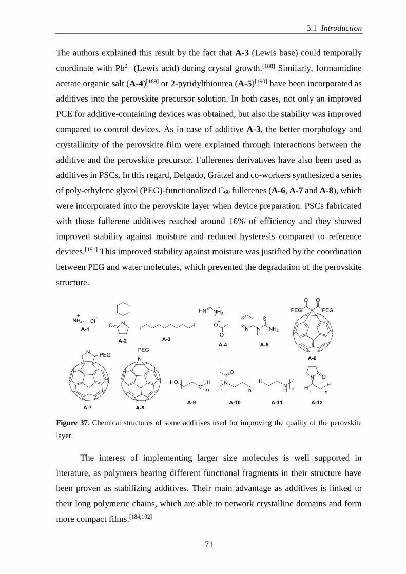
3.1 Introduction
71
The authors explained this result by the fact that A-3 (Lewis base) could temporally
coordinate with Pb2+ (Lewis acid) during crystal growth.[188] Similarly, formamidine
acetate organic salt (A-4)[189] or 2-pyridylthiourea (A-5)[190] have been incorporated as
additives into the perovskite precursor solution. In both cases, not only an improved
PCE for additive-containing devices was obtained, but also the stability was improved
compared to control devices. As in case of additive A-3, the better morphology and
crystallinity of the perovskite film were explained through interactions between the
additive and the perovskite precursor. Fullerenes derivatives have also been used as
additives in PSCs. In this regard, Delgado, Grätzel and co-workers synthesized a series
of poly-ethylene glycol (PEG)-functionalized C60 fullerenes (A-6, A-7 and A-8), which
were incorporated into the perovskite layer when device preparation. PSCs fabricated
with those fullerene additives reached around 16% of efficiency and they showed
improved stability against moisture and reduced hysteresis compared to reference
devices.[191] This improved stability against moisture was justified by the coordination
between PEG and water molecules, which prevented the degradation of the perovskite
structure.
Figure 37. Chemical structures of some additives used for improving the quality of the perovskite
layer.
The interest of implementing larger size molecules is well supported in
literature, as polymers bearing different functional fragments in their structure have
been proven as stabilizing additives. Their main advantage as additives is linked to
their long polymeric chains, which are able to network crystalline domains and form
more compact films.[184,192]

3 Perfluorinated Additives for Perovskite Solar Cells
72
In this regard, Su and co-workers reported the first polymer used as additive for
enhancing the morphology of the perovskite film.[192] They added PEG (A-9) into the
perovskite precursor solution improving the coverage of the perovskite film, which led
to 25% higher PCE of A-9-based PSCs compared to those fabricated without A-9. In
addition, other polymers as poly-(2-ethyl-2-oxazoline) (A-10),[193] polyethylenimine
(A-11)[194] or poly-vinylpyrrolidine (A-12)[195] have been tested as additives in PSCs
leading in all cases to an improvement in the quality of the perovskite layer. In case of
additive A-12, it was incorporated into a CsPbI3-based perovskite, reaching the highest
efficiency of CsPbI3-based PSCs. In addition, PSCs based on this additive showed
excellent thermal and moisture stability.[195]
Semiconducting Chemical Additives
Although additives yield high-quality films, the inherent insulating properties of
most of them can prevent from an efficient transport and extraction of charge carriers.
In this sense, semiconductor additives were also found to improve not only the stability,
but also the device performance of PSCs.[182,196–198]
Figure 38 shows some examples of semiconducting additives used for
stabilizing the perovskite active layer. In this regard, the well-known semiconducting
polymer PCDTBT (HTM-5 in chapter 2) was used as additive and, as a result,
perovskite layers with bigger crystal grains and higher density than control films were
achieved. Moreover, the PCE of additive-containing devices were 16% enhanced
compared to those without additives, with and also improved stability.[182] Similarly,
Ma and co-workers showed that employing conjugated polymers (A-13 and A-15) was
beneficial for achieving improved charge transport along multiple-directions in the
perovskite crystals, resulting in an enhanced efficiency. Besides, the authors showed
that fluorine-containing conjugated polymers (A-14 and A-16) led to further
improvement of the air-stability and photostability of the perovskite due to the
enhanced hydrophobicity of the polymers.[196] The quality of the perovskite layer was
also improved by adding polymers A-17, A-18, A-19 and A-20.[198] PSC efficiencies
using those polymers as additives were improved compared to unmodified devices,
reaching values as high as 19% as well as an improved stability.

3.1 Introduction
73
Figure 38. Chemical structures of semiconductive additives used for improving the quality of the
perovskite layer.

3 Perfluorinated Additives for Perovskite Solar Cells
74
Regarding non-polymeric semiconducting additives, very recently, Song, Kwon
and co-workers used additives A-21 and A-22 to the perovskite layer.[197] A-21- and A-
22- based devices reached 18.7 and 20.3% in efficiency, respectively, which were
higher values compared to those of reference devices (16.7%). The higher stability of
A-22- compared to A-21-based PSCs could be explained by the successful passivation
of the non-coordinated Pb cations of the perovskite crystals by A-22, which led to much
more stables devices compared to control ones. For instance, after 170 hours of
illumination, reference cells maintained only 10% of their initial PCE, while A-22-
based devices kept 84% of their initial PCE. The authors explained the good
performance of additive-based devices by the synergic effect of increasing the quality
of the film and the semiconductor properties of them.
Furthermore, C70 fullerene (A-23) has also found application as additive in
PSCs. Taking advantage of the electron-transporting properties of C70, it was
incorporated into the perovskite precursor solution to fabricate efficient (13.6%) ETL-
free PSCs. C70 doped-perovskite films showed no pinholes (which is the main issue for
ETL-free PSCs) and their integration into PSCs led to more stable devices compared
with the conventional PSCs with TiO2 as ETM.[199] Following this work, a variety of
chemically modified C60 fullerenes (A-24-A-28) showing different electron-accepting
capabilities were used as additives to the perovskite layer to prepare ETL-free PSCs.
Not only have they reached higher efficiencies than those of devices without additives
in the perovskite layer, also they showed an improved stability.[200]
Fluorinated Additives for Perovskite Solar Cells
Taking into account that humidity and thermal instability have a huge impact on
the performance of PSCs, there is a need for materials that can protect them from those
external factors. In this regard, fluorinated compounds generally have excellent
moisture and thermal-resistant properties. In fact, as it has already been proven in
literature, the incorporation of highly fluorinated alkyl chains to materials effectively
enhances the stability to air and temperature, due to the formation of kinetic barriers
against the diffusion of O2 and/or H2O.[201]

3.1 Introduction
75
In this sense, the hydrophobic nature of fluorine-containing organic additives
has demonstrated to protect the perovskite from moisture degradation. Moreover, the
possibility of fluorine atoms of forming hydrogen bonds with the organic cations (A+)
of the perovskite (ABX3), helps to immobilize A cations into the perovskite structure
leading to an improved thermal stability.[202]
Figure 39 shows examples of fluorinated-based additives that have been already
used in PSCs.
Figure 39. Structure of fluorinated-based additives used in PSCs.
For instance, Nazeeruddin, Gao and co-workers showed that a fluorinated
amphiphilic organic salt (A-29) could tune the morphology and enhance the
environmental stability of the perovskite layer which resulted in retarded degradation
of the devices in ambient air.[203] In this regard, A-29 was added into the perovskite
precursor solution and a smoother and more continuous surface than that of pristine
perovskite was achieved. As a result, PSCs based on this new additive showed
improved efficiency (17.9%) as well as enhanced long-term stability compared to PSCs
fabricated without additives. Moreover, the decomposition rate of the MAPbI3
perovskite against moisture was checked by recording X-ray diffraction (XRD)
patterns of perovskite films with and without A-29. It was found that the new phase of
PbI2, which is a decomposition product of MAPbI3, could be seen in both samples after
40 days in 30% relative humidity ambient air. However, the intensity of which the PbI2
phase increased with time was much faster for the undoped perovskite films.

3 Perfluorinated Additives for Perovskite Solar Cells
76
In another work by Ahmad and colleagues, the effect of incorporating an
imidazolium salt additive (A-30), containing a perfluorinated fragment with 9 fluorine
atoms, into the perovskite layer was investigated. A-30-based devices reached 15.4%
in efficiency and a negligible loss in photovoltaic performance after 52 days in ambient
conditions (57-60% relative humidity).[204,205] In the same line, Mathews and co-
workers demonstrated that when the perovskite surface is passivated with
pentafluoropropyl ammonium iodide (A-31), superior moisture stability and improved
device performance was achieved.[206] In this regard, A-31-based PSCs exhibited
enhancement of the PCE from 14.8 (control) to 16.6%, which was attributed to the
larger perovskite crystals and lower surface roughness compared with the standard
perovskite. Moreover, the PCE of the standard device dropped by about 40% from its
initial value, whereas the additive-treated device retained about 94% of its initial value
after 169 days under ambient conditions (55% relative humidity).
Recently, a perylenediimide with two perfluorinated side chains in its structure
(A-32) has been reported as additive for PSCs.[207] The authors investigated the effect
of incorporating additive A-32 into the perovskite layer and not only they achieved an
impressive PCE of 19.3%, but also they demonstrated that adding A-32 led to more
stables PSCs compared to unmodified devices. In fact, A-32-based devices were
subjected to a long-term stability test, in which the cells were kept either in air (50%
relative humidity) or under nitrogen. After 40 days of storage in air, A-32-based
devices maintained over 80% of their initial efficiency while reference devices kept
less than 20% of their initial efficiency. The same tendency was found when devices
were measured after 90 days kept under a nitrogen atmosphere. Moreover, devices
containing A-32 showed better thermal stability than those without it. The hydrophobic
character of additive A-32 would explain the enhancement of the humidity stability,
while F--MA+ interactions, which contribute to immobilize MA cations into the
perovskite structure, would explain the improvement on thermal stability. The
improved efficiency and stability of A-32-incorporated devices could be explained by
an improvement on the quality of the perovskite layer. First, the fluorine anions in A-
32 can interact with MA cations creating hydrogen bonds between them, which retards
crystallization and as a result, larger grain size and less grain boundaries as well as

3.1 Introduction
77
reduced pinholes were obtained. Second, A-32 can effectively passivate trap states
because the carbonyl groups in its structure can chelate with non-coordinated Pb2+.
It can be concluded that by treating the perovskite layer with fluorinated
additives, the access of moisture into the perovskite layer can be significantly
suppressed. Moreover, it is worth mentioning that in all the examples, fluorine-
containing devices showed negligible hysteresis which could be explained by the
reduction of ion migration due to the fluorine-organic cation (perovskite) interactions,
previously mentioned.

3 Perfluorinated Additives for Perovskite Solar Cells
78
3.2 Objectives
All the aforementioned examples soundly demonstrate that carefully-designed
additives are able to significantly affect the crystallization kinetics of perovskites,
suppress trap formation, tailor and improve optoelectronic properties. All this
eventually leads to enhanced lifetime of the devices and often improves the
photovoltaic performance of PSCs. In addition, the advantage of compatibility of the
additive with the perovskite material has been demonstrated, so additives with
semiconductive properties are highly desired in order to favour charge transport. On
the other hand, the lack of examples of additives with large perfluorinated units in the
literature, together with our interest to know if these compounds could improve the
overall performance of PSCs, motivated the beginning of this research work.
With all this in mind, we have proposed as main objective of this chapter the
design, synthesis and application of three perfluorinated semiconducting organic
materials as novel dopants or additives for PSCs. In order to achieve the main objective,
other tasks more specific were defined:
Design and synthesis of a small molecule and two polymeric materials which
contain highly perfluorinated chains in their structure (26 fluorine atoms per unit). The
structure of the compounds will be confirmed by NMR and mass spectrometry while
the molecular mass distribution of the two polymers will be determined by SEC.
Characterization of the newly compounds by thermal, optical and
electrochemical techniques in order to evaluate their properties. In this regard, the
newly materials should have optimal HOMO levels in order to not hinder the hole
transport, and in that way, favouring the hole transport from the perovskite to the
electrode. In addition, they should have minimal absorption in the visible region.
The novel additives will be incorporated into the perovskite precursor solution
and their effect on the film formation, stability and performance of PSCs will be
investigated.

3.3 Results and Discussion
79
3.3 Results and Discussion
3.3.1 Design and Synthesis of Additives S1, P7 and P8
Figure 40 displays the chemical structures of the proposed compounds. We have
designed a novel small molecule (S1) and two polymeric compounds (P7 and P8)
which contain 26 fluorine atoms per unit.
Figure 40. Chemical structures of the target compounds S1, P7 and P8.
The addition of an additive into the perovskite layer could affect the energy
levels or the interface between the HTM and the perovskite and increases the transport
resistance, which would reduce the efficiency of the resulting PSC.[179] For this reason,
to facilitate charge transport and extraction in the perovskite layer and to guarantee
optimal photovoltaic performance, all compounds derive from the family of
triarylamines, which are one of the most used p-type organic semiconductors. Molecule
S1 contains two triarylamine units, attached to a central benzyl ring, which bears two
perfluorinated chains, each one containing 13 fluorine substituents. Polymers P7 and
P8 are composed of a perfluorinated benzyl unit in combination with two different
donor moieties, a triaryalmine and a triarylamine extended unit, respectively. Both
polymers benefit from the enhanced solubility given by the introduction of alkyl groups
in their structures, making them easier to process. To the best of our knowledge, the

3 Perfluorinated Additives for Perovskite Solar Cells
80
three novel materials contain the largest amount of fluorine atoms reported for
additives in PSCs.
The electron rich methoxy groups in S1 and oxygen-containing fragments in P7
and P8 are expected to enhance the supramolecular interaction between the perovskite
and the additive via hydrogen bonding and passivate non-coordinated Pb2+.[184,185]
Synthesis of Intermediates
For the synthesis of the various additives S1, P7 and P8, it was necessary to
synthesize different functionalized monomers (M2, M6 and M7) or intermediates (11)
containing bromine or boronic ester groups (Figure 41). These functionalized
molecules will allow us in a further step use Pd-catalyzed Suzuki cross coupling
reaction for obtaining the target compounds.
Figure 41. Chemical structures of monomers (M2, M6 and M7) and intermediate 11.
The synthesis of monomer M6, which bears the perfluorinated chains, was
carried out by following reported procedures (Scheme 8).[208] First, the reaction of 1,4-
diiodobenzene with an excess of perfluorohexyl iodide in dimethyl sulfoxide (DMSO)
gave 1,4-bis(perfluorohexyl)benzene (9) in high yield. Then, the treatment of
compound 9 with NBS in acidic media led to the desired monomer M6.
Scheme 8. Synthesis of monomer M6 functionalized with bromine groups and bearing the
perfluorinated chains.

3.3 Results and Discussion
81
Monomer M7 was synthesized by Miyaura coupling of the dibrominated
monomer M3, previously synthesized, and bis(pinacolato)diboron using PdCl2(dppf)
as catalyst (Scheme 9).
Scheme 9. Synthesis of monomer M7.
Finally, the synthesis of intermediate 11 was carried out following a two-step
synthetic procedure, as shown in Scheme 10. First, the Ullmann reaction of 4-
bromoaniline and 4-iodoanisole gave triaryalmine 10 following a reported
procedure.[209] Then, intermediate 11 was obtained by Miyaura borylation of compound
10 in moderate yield.
Scheme 10. Synthesis of intermediate 11.
The synthesis of monomer M2 was already described in page 50.
Synthesis of Additives S1, P7 and P8
The novel compounds S1, P7 and P8 were then synthesized by Suzuki coupling
reaction. Perfluorinated monomer M6 was coupled with two molecules of borylated
triarylamine 11 through Suzuki cross coupling, using Pd(PPh3)4 as catalyst in
anhydrous toluene to obtain S1 (Scheme 11).

3 Perfluorinated Additives for Perovskite Solar Cells
82
Scheme 11. Synthesis of small molecule S1.
The composition and chemical structure of the synthesized compound S1 was
confirmed by 1H NMR, 13C NMR, 19F NMR and mass spectrometry (ESI). Further
evidences of the presence of compound S1 were found by tracking the changes in the
19F NMR spectrum originating from perfluorinated chains, which occur after the
coupling of compound M6 with triarylamine 11. Figure 42 shows the 19F NMR
spectrum of monomer M6.
Figure 42. 19F NMR spectra (376 MHz, CD2Cl2, 298 K) of M6, S1, P7 and P8.
At room temperature, the spectrum exhibits the usual pattern of an aromatic-
bonded C6F13 group, with the appropriate number of 19F resonance signals.[210] The
signal at -107.75 ppm is attributed to the fluorine atoms closer to the aromatic ring,
denoted as a. The rest of fluorine atoms of M6, which are denoted as b-e, are all
assigned to the structure as can be seen in Figure 42. After the coupling between

3.3 Results and Discussion
83
compound M6 and triarylamine 11, the resonance signal a, shifts to approximately -
103.25 ppm in molecule S1, as a consequence of the deshielding effect of the new
substituent. (Figure 42).
The mass analysis revealed that for S1 a molecular peak for [M + H]+ :1321.249
was detected (Figure 43).
Figure 43. ESI-TOF of molecule S1.
Similarly, polymers P7 and P8 were synthesized by Suzuki coupling
polymerization of the corresponding diboronic ester monomers M2 and M7,
respectively, with monomer M6 in the presence of Pd(PPh3)4 in toluene using NaHCO3
as base (Scheme 12).
Scheme 12. Synthesis of the target polymers P7 and P8.
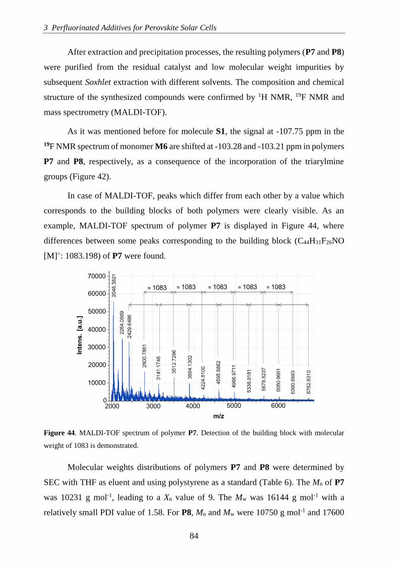
3 Perfluorinated Additives for Perovskite Solar Cells
84
After extraction and precipitation processes, the resulting polymers (P7 and P8)
were purified from the residual catalyst and low molecular weight impurities by
subsequent Soxhlet extraction with different solvents. The composition and chemical
structure of the synthesized compounds were confirmed by 1H NMR, 19F NMR and
mass spectrometry (MALDI-TOF).
As it was mentioned before for molecule S1, the signal at -107.75 ppm in the
19F NMR spectrum of monomer M6 are shifted at -103.28 and -103.21 ppm in polymers
P7 and P8, respectively, as a consequence of the incorporation of the triarylmine
groups (Figure 42).
In case of MALDI-TOF, peaks which differ from each other by a value which
corresponds to the building blocks of both polymers were clearly visible. As an
example, MALDI-TOF spectrum of polymer P7 is displayed in Figure 44, where
differences between some peaks corresponding to the building block (C44H31F26NO
[M]+: 1083.198) of P7 were found.
Figure 44. MALDI-TOF spectrum of polymer P7. Detection of the building block with molecular
weight of 1083 is demonstrated.
Molecular weights distributions of polymers P7 and P8 were determined by
SEC with THF as eluent and using polystyrene as a standard (Table 6). The Mn of P7
was 10231 g mol-1, leading to a Xn value of 9. The Mw was 16144 g mol-1 with a
relatively small PDI value of 1.58. For P8, Mn and Mw were 10750 g mol-1 and 17600

3.3 Results and Discussion
85
g mol-1, respectively, with a PDI of 1.64 and Xn of 8. It is worth mentioning that during
the optimization of the synthetic procedures, we have been able to obtain fractions with
higher molecular weights as Mn of 18563 gmol-1 corresponding to Xn of 17 for P7 or
Mn of 25764 gmol-1 (Xn = 19) in case of polymer P8. However, for the current study,
fractions characterized by Xn = 9 and Xn = 8 for P7 and P8, respectively, were
employed.
Polymer Mn (g mol-1) Mw (g mol-1) Xn PDI
P7 10231 16144 9 1.58
P8 10750 17600 8 1.64
Table 6. Molecular weights of polymers P7 and P8.
As expected, the perfluorinated chains modify the solubility of the compounds
due to the hydrophobic nature of the substituents. The compounds are insoluble in
EtOH and MeOH, show low solubility in DMF, DMSO and acetone and moderate
solubility in chlorobenzene and chloroform (5 mg mL-1).
To characterize the hydrophobicity of S1, P7 and P8, water contact angle
measurements of spin-coated films of the compounds were carried out. Hydrophobicity
is commonly characterized by the water contact angle which is higher than 90° for
hydrophobic surfaces and higher than 150° for superhydrophobic surfaces.[211] The
contact angles of the water droplet were 107°, 106° and 102º for S1, P7 and P8,
respectively, demonstrating the outstanding hydrophobic nature of the compounds
(Figure 45).
A)
B)
C)
Figure 45. Water contact angles of A) molecule S1, B) polymer P7 and C) polymer P8.

3 Perfluorinated Additives for Perovskite Solar Cells
86
3.3.2 Thermal, Optical and Electrochemical Properties
a) Thermal properties
TGA analysis carried out at a heating rate of 10 °C min-1 under nitrogen
atmosphere indicated the high thermal stability of molecule S1 and polymers P7 and
P8 (Figure 46A). Additives S1, P7 and P8, showed Td at 249, 284 and 274 ºC,
respectively (Table 7), which were well above operational conditions of PSCs. All
compounds exhibited a weight loss before decomposition, which was attributed to the
loss of solvent traces.
A)
B)
C)
Figure 46. A) Thermogravimetric heating curves of compounds S1, P7 and P8 (heating rate 10 °C
min-1). B) Differential scanning calorimetry of the second heating curves for polymers P7 and P8
(heating rate 20 °C min-1).C) Differential scanning calorimetry curves for molecule S1 at a scan rate
of 20 °C min-1.

3.3 Results and Discussion
87
DSC measurements revealed that polymers P7 and P8 were fully amorphous
showing Tg values at 81 and 82 ºC, respectively (Figure 46B). In contrast, molecule S1
showed only a peak corresponding to the melting of the material at 194 °C during the
first heating, and no glass transition was detected upon heating. During the cooling, an
exothermic process of crystallization was observed at 153 °C indicating that below that
temperature the material was crystalline. In the second heating process, the melting of
the material was observed again, but no crystallization process, because the material
was already crystalline (Figure 46C).
Sample Td (°C) [a] Tg (°C) [b] Tm (°C) [c] Tc (°C) [d]
S1 248.89 - 193.97 153.26
P7 284.04 80.92 - -
P8 274.10 81.85 - -
Table 7. Thermal properties of molecule S1 and polymers P7 and P8. [a] Decomposition temperature
determined from TGA (2 % weight loss). [b] Glass transition temperature determined from DSC
(second heating curve). [c] Melting temperature determined from DSC (first or second heating curve).
[d] Crystallization temperature determined from DSC (cooling curve).
b) Optical properties
The UV-vis absorption spectra of S1, P7 and P8 are shown in Figure 47A and
the absorption spectrum of polymer P6 are depicted for comparison with that of
polymer P8 (Figure 47B). As expected, all compounds did not display significant
absorption in the visible region. On the other hand, these materials presented strong
absorption in the UV region, with λmax,abs around 300-330 nm. The Ɛ value at the
absorption maximum of S1 was around 40000 M-1 cm-1 while for polymers P7 and P8
were around 20000 and 30000 M-1 cm-1, respectively (Table 8).
Introducing more electron-withdrawing groups on the structure of a molecule
makes λonset and λmax,abs values of the molecule blue-shifted. For example, the λonset and
λmax,abs values of polymer P8 are 12 nm and 20 nm blue-shifted from those of polymer
P6 (synthesized in chapter 2), respectively. This leads to a widening in the energy band
gap, as is shown in Table 8. This behaviour was already reported.[212] In case of polymer
P7, with less phenyl rings in its backbone than polymer P8, a shorter λmax,abs value

3 Perfluorinated Additives for Perovskite Solar Cells
88
compared to P8 was found (Table 8). Finally, molecule S1, with less conjugated
systems than the polymers, has the shortest λmax,abs value among the 3 new compounds,
which is centred at 302 nm.
A)
B)
Figure 47. A) Absorption spectra of S1, P7 and P8 in DCM. B) Comparison of normalized UV-vis spectra of
polymers P6 and P8 in DCM.
The Eg values, estimated from the absorption spectra, of S1, P7 and P8 were
practically equal with values of 3.07 eV for S1 and P7 and 3.02 eV for P8 (Table 8).
Sample λmax,abs (nm) Ɛ (M-1cm-1) λonset (nm) Eg (eV)
S1 302 39458 404 3.07
P7 311 18375 404 3.07
P8 329 31305 411 3.02
P6 349 26586 423 2.93
Table 8. Optical properties of compounds S1, P7 and P8.
c) Electrochemical properties
The electrochemical properties of molecule S1 and polymers P7 and P8 were
studied by CV, measured in a 0.1 M solution of TBAHFP in anhydrous DCM (Figure
48A). Their EHOMO values were obtained from EonsetOx1 during CV measurements using
the Fc/Fc+ redox couple as the internal standard. Therefore, EHOMO is calculated
according to the equation 17 and the data is listed in Table 9.

3.3 Results and Discussion
89
A)
B)
Figure 48. A) Cyclic voltammograms of S1, P7 and P8 in DCM/TBAHFP (0.1 M) at a scan rate of
250 mV s-1. B) Energetic levels of polymers S1, P7, P8 and perovskite light absorber layer used in this
study.
S1 and P7 exhibited one reversible oxidation wave at E1/2Ox1 values of 0.34 and
0.51 V vs Fc/Fc+, respectively, indicating their electrochemical stability. The EonsetOx1
values at 0.29 and 0.40 V values for S1 and P7, respectively, led to EHOMO levels of -
5.09 and -5.20 eV, respectively. As the EHOMO for the triple cation perovskite, used in
this work, is -5.45 eV,[168] a possible hole transfer from the perovskite to the donor is
possible which implies that both additives would not impede the charge transport
within the perovskite material (Figure 48B). Thus, with the above absorption onset at
3.07 eV for both compounds S1 and P7, the ELUMO values were estimated to be -2.02
and -2.13 eV, respectively.
For polymer P8 two different oxidation waves were observed, being the second
one no reversible. The strong electron-donor properties of polymer P8 compared to
polymer P7 was reflected in the decreasing of its first oxidation potential by 0.41 V
compared to P7. With an EonsetOx1
value of -0.01 V an EHOMO of -4.79 eV was obtained,
that in combination with the above calculated Eg led to an ELUMO value of -1.77 eV. As
in compounds S1 and P7, polymer P8 exhibited good band alignment with the VB of
the perovskite (Figure 48B), not hindering the transport of charges.

3 Perfluorinated Additives for Perovskite Solar Cells
90
Sample E1/2Ox1(V) Eonset
Ox1 (V) EHOMO (eV) ELUMO (eV)
S1 0.34 0.29 -5.09 -2.02
P7 0.51 0.40 -5.20 -2.13
P8 0.05 -0.01 -4.79 -1.77
Table 9. Electrochemical properties and energy levels of S1, P7 and P8.
3.3.3 Perovskite Solar Cells Employing S1, P7 and P8
To investigate the role of compounds S1, P7 and P8 in the perovskite film, these
materials were incorporated into the perovskite layer as additives in regular planar
devices. This study was carried out in collaboration with Dra. Nevena Marinova from
the Hybrid Materials for Photovoltaics Group (Polymat, San Sebastián, Spain).
Perovskite-Based Device Fabrication
The solar cell architecture, depicted in Figure 49, was composed of
FTO/SnO2/Perovskite+additive (S1, P7 or P8)/spiro-OMeTAD/Au, where the SnO2
and spiro-OMeTAD acted as electron- and hole-transport layers, respectively.
Figure 49. Simplified model of the perovskite-based solar cell used for testing additives S1, P7 and
P8 and cross sectional SEM image of a device with S1 as additive.

3.3 Results and Discussion
91
The additives were simply added with the weight concentration of 2 mg mL-1 to
a precursor solution of the perovskite with the composition FAI (1 M), CsI (0.05 M),
PbI2 (1.1 M), MABr (0.2 M) and PbBr2 (0.22 M) in DMF:DMSO (4:1) solvent mixture.
The perovskite used in this study was the triple cation perovskite of the generic form
“Cs0.05(MA0.17FA0.83)0.95Pb(I0.83Br0.17)3”.
The cell architecture of the fabricated device using molecule S1 as additive can
be appreciated from the SEM cross-sectional image displayed in Figure 49.
Photovoltaic Device Testing
PSCs using compounds S1, P7 and P8 as additives within the perovskite were
fabricated and tested under simulated AM 1.5G illumination at 100 W cm-2 with
masking aperture of 0.16 cm2. Figure 50 shows the J-V curves of the highest
performance PSCs.
Figure 50. J-V curves for the best performing PSCs using compound S1, P7 and P8 as additives.
The statistics for the device parameters are shown in Figure 51 and Table 10
summarizes the photovoltaic characteristics of the resulting devices.
The reference devices showed average PCE of 14% with maximum value of
15.9%. Doping the perovskite material with S1 slightly decreased the average PCE,
mainly due to reduced Voc and FF. However, some of the S1-devices deviated from
this trend, showed high current and record efficiency, reaching 17% (Table 10). The
P7-doped PSCs showed Voc comparable with reference devices and PCEs slightly
lower. Finally P8-doped perovskite devices had a FF and Jsc similar to reference

3 Perfluorinated Additives for Perovskite Solar Cells
92
devices, while the Voc was slightly lower than in reference devices, as in case as
polymer P7. In general, doping the perovskite with additives S1, P7 and P8 slightly
affected the device performance, which implies that the semiconductor properties of
the perovskite, such as charge transport, were unaffected.
Figure 51. Comparison of the devices parameters for reference and perovskite solar cells with S1, P7
and P8. Whiskers show minimum and maximum values, box represents the values between 25% and
75% and circles show mean values.
Sample VOC (V) JSC (mA cm-2) FF (%) PCE (%)
Ref 1.09 (1.05) 17.5 (20.1) 74 (75) 14.1 (15.9)
S1 1.06 (1.09) 17.9 (20.6) 72 (76) 13.7 (17.0)
P7 1.09 (1.12) 17.6 (18.3) 72 (74) 13.9 (15.1)
P8 1.06 (1.07) 17.3 (18.2) 74 (74) 13.6 (14.4)
Table 10. Average photovoltaic parameters devices determined form J-V measurements using S1, P7
and P8 as additives in PSCs. The photovoltaic parameters of the best working cells are shown in
brackets.
One of the main limitations to the advancements of PSCs is the presence of
hysteresis in the J-V curves depending if the measurement is carried out with forward
or reverse scan. The hysteric behaviour of the devices tends to vary from batch to batch

3.3 Results and Discussion
93
independent of the devices type. In case of devices prepared in this study, frequently,
all the devices from certain batch showed no hysteresis (Table 11). In order to quantify
the hysteresis magnitude the hysteresis index (HI) is used, as reported in literature.[213]
The HI for the cases when PCE (reverse) > PCE (forward) is calculated using equation
18, while for cases when PCE (reverse) < PCE (forward), equation 19 is used:
HI = [Pmax,r/Pmax,f]-1 (18)
HI = [Pmax,f/Pmax,r]-1 (19)
Where Pmax,f and Pmax,r are the maximum power points on the forward and the
reserve scan, respectively.
Sample Device Scan
direction
VOC
(V)
JSC
(mA cm-2)
FF
(%)
PCE
(%)
P
(mW) HI
Ref
A F 1.08 16.93 72.55 13.20 2.11
0.03 R 1.07 16.79 72.26 13.55 2.17
B F 1.07 16.81 73.71 13.28 2.13
0.01 R 1.07 16.74 73.42 13.11 2.10
C F 1.07 17.64 72.68 13.75 2.20
0.04 R 1.07 17.55 76.37 14.33 2.29
S1
A F 1.05 16.85 72.87 12.84 2.05
0.00 R 1.04 16.74 74.04 12.83 2.05
B F 1.03 17.64 72.21 13.17 2.11
0.04 R 1.03 17.61 75.57 13.68 2.19
C F 1.03 16.62 71.97 12.30 1.97
0.02 R 1.02 16.61 74.18 12.56 2.01
P7
A F 1.08 17.22 72.31 13.41 2.15
0.01 R 1.06 17.14 74.30 13.54 2.17
B F 1.06 17.75 72.14 13.58 2.17
0.02 R 1.05 17.74 71.70 13.35 2.14
C F 1.08 17.42 74.33 13.92 2.23
0.03 R 1.05 17.24 74.86 13.56 2.17
P8
A F 1.07 16.61 73.41 13.08 2.09
0.01 R 1.06 16.54 75.08 13.16 2.11
B F 1.06 17.75 72.91 13.74 2.20
0.02 R 1.05 17.69 72.57 13.42 2.15
C F 1.07 28.21 73.64 14.38 2.30
0.02 R 1.06 18.07 73.61 14.07 2.25
Table 11. Examples of hysteresis index from one batch. F= forward scan; R= reverse scan.

3 Perfluorinated Additives for Perovskite Solar Cells
94
As is shown in Table 11, for this batch, no significance hysteresis could be
observed, being even cero for a S1-doped device.
However, there are some batches, in which all the devices showed hysteresis in
the J-V curves. We attributed this alteration to variation in the quality of the SnO2
electron-transport layer for every batch, due to low reproducibility of the layer
formation.
Film Characterization
a) X-ray diffraction analysis
In order to confirm the structure of the perovskite films, XRD measurements
were performed. Figure 52 shows the diffractograms of pristine perovskite and doped
perovskite films with S1, P7 and P8 deposited onto a FTO glass substrate. All films
displayed the typical pattern for perovskite, with the most pronounced peaks at 2θ =
14.16º and 28.5º corresponding to the (110) and (220) planes of the perovskite,
respectively.[214] The same diffraction peaks for all perovskite films indicated that
additives were not embedded in the perovskite crystal lattice and could only exist at
GBs or surface of perovskite films.[207]
Figure 52. X-ray diffractograms of pristine perovskite (Ref) and doped perovskite with S1, P7 or P8
deposited on FTO covered glass. Peaks marked with P corresponds to PbI2, F to FTO and * to
perovskite.
The increased peak intensity at 2θ = 14.16º for P7-doped layer suggests
improved crystallinity of the perovskite.[215] Due to the slight excess of PbI2, all samples

3.3 Results and Discussion
95
displayed a small peak at 12.7º.[173] This peak, however, decreased slightly in intensity
with the addition of additives S1 and P7 suggesting an improved conversion.
b) Optical properties
The UV-vis absorption spectra of pristine perovskite and S1, P7 or P8-doped
perovskite deposited onto FTO/SnO2 substrates are shown in Figure 53. All films
displayed the typical for triple cation perovskite absorption and are practically
identical, so the deposition of the hydrophobic compounds (S1, P7 or P8) did not
compromise the absorption of the perovskite. Moreover, the intrinsic characteristics of
the perovskite were not influenced by a small amount of these novel perfluorinated
materials.
Figure 53. UV-vis absorption spectra of FTO/SnO2/perovskite film (Ref) and
FTO/SnO2/perovskite+S1, P7 or P8 films.
c) Water contact angle measurements
To assess the effect of the dopants on the hydrophobicity of the perovskite we
performed water contact angle measurements of pristine perovskite and perovskite
doped with S1, P7 and P8 deposited onto FTO/SnO2 substrates. We recorded contact
angles of 56° for the pristine perovskite versus measured angles of 68°, 62° and 60º for
S1-, P7- and P8-doped perovskite, respectively (Figure 54). This result showed that the
surface of the perovskite layer was modified by the hydrophobic compound and that
the compounds were embedded in the perovskite film and/or on its surface.

3 Perfluorinated Additives for Perovskite Solar Cells
96
A) FTO/SnO2/pvsk
C) FTO/SnO2/pvsk + P7
B) FTO/SnO2/pvsk + S1
D) FTO/SnO2/pvsk + P8
Figure 54. Water contact angle measurements after dropping water onto A) FTO/SnO2/perovskite film,
B) FTO/SnO2/perovskite+S1 film, C) FTO/SnO2/perovskite+P7 film and D) FTO/SnO2/perovskite+P8
film
d) Scanning electron microscopy measurements
Figure 55 shows top-view SEM micrographs of the prepared pristine perovskite
film and those of films doped with S1, P7 or P8. As can be seen, films were composed
of perovskite grains, which in the pristine perovskite appear to be clearly faceted with
sharp edges and GBs. The doped perovskite layers were composed of grains with
slightly bigger size and reduced grain boundaries. This trend is especially pronounced
for the case of polymer P7-doped perovskite.
Figure 55. Top-view SEM micrographs of the pristine perovskite film and the doped-perovskite film
with S1, P7 or P8. The perovskite film were deposited onto SnO2/FTO substrate.

3.3 Results and Discussion
97
To quantify the effect of the additives on the film morphology and grain size we
analyzed the SEM micrographs with an image-process software. Table 12 contains the
grain size parameters obtained from the micrographs. The mean grain diameter of the
reference perovskite is 160 nm, which was consistent with previously reported data for
this type of perovskite.[98] The addition of S1, P7 or P8 into the perovskite layer led to
an increase in mean grain size to 195 nm for S1-doped-perovskite, above 200 nm for
P7-doped perovskite and to 173 nm for P8-doped perovskite. The increment of the
grain size and improved perovskite quality is frequently observed when suitable
additives are employed. The reason for this is that in the presence of small quantities
of additives, the formation of disordered gel-sol precursor phase is promoted during
the process of crystallization and grain growth, more specifically during the early stage
of the spin-coating. This disordered precursor phase slows down the crystallization
process, which results in larger grains.[198,216]
Sample Mean Area (nm²) Mean Diameter (nm)[a] Particle counts[b]
Ref 22286 159 682
S1 33699 195 431
P7 38331 207 379
P8 26535 173 575
Table 12. Grain parameters of the reference perovskite film and perovskite films doped with S1, P7
and P8. [a] The diameter is expressed as the diameter of a circle having an area equal to the area
enclosed by the shape’s contour. [b] The analyzed area is the same for all the images. The reduced
particle number reflects the increased particle size.
It is worth to say that we cannot affirm that the less increment in grain size when
the perovskite film is doped with polymer P8 comparing with the other two additives
(S1 and P7), is due to the material itself. Polymer P8 turned to be very insoluble in the
DMSO:DMF perovskite precursor solution, so it is highly likely that the concentration
of this compound in the perovskite layer is much less than that achieved with the other
two additives. For this reason, at this point, we decided to continue the study without
polymer P8.

3 Perfluorinated Additives for Perovskite Solar Cells
98
e) Atomic force microscopy measurements
To further investigate the effects of doping in the perovskite layer, morphology
of pristine perovskite and doped perovskite (with S1 or P7) films were also study by
atomic force microscopy (AFM). The difference in shape was also evident from the
topography and phase images derive from those measurements (Figure 56). As can be
seen, the undoped perovskite was composed of smaller, cuboid-like grains with
pronounced edges, which affected the surface of the film. S1- and P7-doped perovskite
films, in contrast, showed smoother edged and round-shaped flat grains with reduced
grain boundaries. From AFM topography images, we obtained the root mean square
roughness, which were 12.8, 11.9 and 11.8 nm for pristine perovskite, S1-doped
perovskite and P7-doped perovskite, respectively. The lower roughness value for
doped-perovskite layers indicates a smoother and more uniform layers than that of
pristine perovskite.
A)
B)
C)
Figure 56. Top: Topography AFM micrographs of A) pristine perovskite film, B) S1-doped perovskite
film and C) P7-doped perovskite film deposited onto FTO/SnO2 substrates. Bottom: AFM phase
images of the surface of A) pristine perovskite film, B) S1-doped perovskite film and C) P7-doped
perovskite film deposited onto FTO/SnO2 substrates.

3.3 Results and Discussion
99
Stability Tests
To better clarify the effect of the incorporation of the additives on the stability
of the devices, we performed stability tests of PSCs using molecule S1 and polymer P7
as additives to the perovskite layer.
We carried out two types of stability measurements in air without encapsulation.
In the first experiment, the power output was measured for 80 minutes using pristine
perovskite and doped-perovskite layers (with S1 or P7) in corresponding devices.
During the measurement, we measured their stabilized power output keeping the solar
cells at bias close to their maximum power point (MPP)1. The measurement was carried
out in air in the solar simulator. As shown in Figure 57A, the reference device started
degrading gradually since the beginning of the measurement and after 40 minutes
severe degradation issues were observed. This led to the complete breakdown of the
device after 80 minutes of operation under these conditions. In contrast, S1-doped
devices showed very stable power output practically without any decay for about 40
minutes. Then, the power started to decline slowly and after 80 minutes of aging in air
the device maintained 94% of the initial power. P7-doped devices showed gradual
decrease of output power, which was delayed compared to reference devices and
reached 85% of its initial power after 80 minutes.
A)
B)
Figure 57. A) Normalized power measured as a function of time for reference and stabilized cells kept
at MPP in air. B) Normalized PCE measured for reference and stabilized devices storage in air.
1 When a solar cell receives solar radiation, it produces power, which is the product of current
and voltage. The highest power output for a solar cell is called maximum power point (MPP)

3 Perfluorinated Additives for Perovskite Solar Cells
100
In the second experiment, stability assays of pristine perovskite and S1- or P7-
doped perovskite devices upon storage in air (50-70% relative humidity) were also
performed. The normalized PCE as a function of storage time is shown in Figure 57B.
As can be seen, substantial differences in stability were noted for doped devices
compared to the reference device. The PCE of the reference device dropped to 54% of
their initial value after 16 days of storage. S1- and P7-doped devices kept 86% and
60% of their initial PCE, respectively. This result further demonstrated the stabilizing
effect of the novel perfluorinated dopants. The weaker stabilization effect of P7
compared to S1 could be explained by the Tg value of the polymer. In this sense, after
perovskite deposition, an annealing process at 100 °C was carried out, which could
lead to phase transition of the polymer, which could alter the morphology of the
perovskite film.
It was already mentioned that perovskite devices are very sensitive when
operating in ambient air and they degrade quickly due to a number of degradation
processes related to the effect of oxygen, humidity, temperature among others, in the
solar cell stack.[170,217–220] Doping the perovskite with the perfluorinated additives
modifies the surface, thus increasing the hydrophobicity of the perovskite and
providing a protective barrier for the oxygen, which retards the degradation when
devices are operating in air. Furthermore, prolonged operation causes heating of the
device. In this study, we have measured the temperature of the cavity in the solar
simulator where devices were measured in prolonged experiment, and we observed that
in less than 10 minutes the temperature of the air in the measuring cavity set to 46°C
and remained constant (Figure 81, experimental part). This inevitably caused heating
of the devices, without taking into account the intrinsic heating of a solar cell due to
resistive effects, etc. Therefore, we can hypothesize that the perfluorinated dopants
retard the degradation of the devices when operating in air under elevated temperature
(higher than the standard measuring conditions) also due to improved thermal stability.
This is consistent with previous studies, which report that perfluorinated compounds
enhance the thermal stability of the materials.[221]

3.4 Conclusions
101
3.4 Conclusions
In summary, three novel perfluorinated additives (S1, P7 and P8) for PSCs have
been developed. The compounds were successfully synthesized and their chemical,
thermal and optoelectronic properties studied. The novel additives contain 26 fluorine
atoms per unit, which is the largest amount of fluorine atoms reported for additives in
PSCs. The presence of those perfluorinated chains increases the hydrophobicity of the
perovskite when adding to the material in very small quantity. Additives were
incorporated into the perovskite layer and the overall effect of the compounds in PSCs
was studied. Fluorine-containing organic additives are known to provide thermal
stability to the materials as well as protection against humidity and oxygen due to their
hydrophobicity, while at the same time improve the morphology of the perovskite
layer. In this regard, the doped-perovskite films showed larger crystals and reduced
GBs compared to the undoped one. Moreover, the stability of devices based on
additives S1 and P7 were studied and as a result, S1- or P7-based devices showed
increased stability, maintaining 86% and 60% of their initial performance, respectively,
after 16 days of exposure to ambient atmosphere (50-70% relative humidity). The
stabilizing effect is most likely due to combined protective action against humidity and
oxygen, because of the formation of a protective barrier by the perfluorinated
compound. Nevertheless, the stabilization upon heating under operation could also be
considered as a possible mechanism of action. Importantly, the semiconducting nature
of the novel additives might be favouring charge transport, leading to efficiencies
comparable to reference devices, and allowing S1-containing device to achieve an
improved PCE value (17.0%) compared to the reference device. However, the novel
compounds showed low solubility in the perovskite precursor solution, which limited
their application in higher concentration. Therefore, improved molecular design and
synthesis of perfluorinated compounds with increased compatibility with the precursor
solution and increased Tg would be required to further explore the full potential of
perfluorinated compounds in PSCs. Overall, these new perfluorinated compounds are
presented as excellent additive candidates towards stable and efficient PSCs.


4. ELECTRON-TRANSPORTING
POLYMERS FOR PEROVSKITE
SOLAR CELLS


4.1 Introduction
105
4 ELECTRON-TRANSPORTING POLYMERS FOR PEROVSKITE
SOLAR CELLS
4.1 Introduction
In contrast to widely investigated HTMs, a fewer types of ETMs have been
developed. However, ETMs play also a crucial role in both regular and inverted PSC
architectures, so the exploration of novel ETMs is also necessary.
In this chapter a discussion on ETM requirements together with an overview of
the developed materials used as ETMs for PSCs are highlighted, which in a further step
will help us to design new ETMs for perovskite-based devices.
4.1.1 Role and Properties of Electron-Transporting Materials in PSCs
The main function of an ETM is the extraction of the photogenerated electrons
from the perovskite and transporting them to the electrode, although it has many other
important contributions. For instance, as mentioned previously, in the course of a PSC
operation, undesirable processes can occur, such as recombination of the charge
carriers at the interfaces, that in case of taking place would lead to a reduction in the
device performance.[222] In this regard, the ETM could help to avoid these processes by
serving as hole-blocking layer, suppressing charge recombination at the
perovskite/ETM interface.[223] Moreover, the ETM can act as a barrier against external
factors, such as oxygen or moisture, and in that way protecting the perovskite from
them. In regular-type PSCs the ETM is a vital component since it will determine the
final quality of the perovskite layer, because is the substrate in which the perovskite is
deposited.[224] Although there have been already reported ETL-free devices, the
incorporation of ETMs in PSCs is still necessary in order to achieve efficient and stable
PSCs.[225,226]
In order to obtain high-performance PSCs, an ETM should satisfy some general
requirements: (i) The energy levels of the ETM should be well-aligned with those of
the active perovskite layer and with the work function of the electrode. In this regard,

4 Electron-Transporting Polymers for Perovskite Solar Cells
106
the LUMO level of the ETM should be lower than the CB of the perovskite in order to
facilitate electron extraction and transport. On the other hand, the HOMO of the ETM
should be lower than the VB of the perovskite to fulfil the hole-blocking function,
avoiding recombination losses, as above-mentioned.[227] (ii) Moreover, a relatively
high electron mobility/conductivity is also needed for an efficient charge transport.[228]
(iii) ETMs should show good chemical stability as well as good photo and thermal
stability.[227,229] (iv) They should have enough solubility in the appropriate solvent and
good-film forming ability for processing and device fabrication. In this sense, a high-
quality pinhole-free dense ETL layer with few defects and seamless interface with
other layers is desirable for high-performance PSCs.[227,228,230] (v) An ideal ETM should
not suffer any phase transition during device fabrication/operation. (vi) They should be
cheap and environmental friendly. (vii) The Eg of the ETM should be wide enough to
ensure transparency and allow light to pass through, while not competing with the
perovskite in light absorption.[231]
4.1.2 Organic Electron-Transporting Materials for PSCs
Taking into account that PSCs were first developed based on DSSCs, in which
TiO2 acts as an ETM, it is not surprising that TiO2 was used in the first perovskite-
based device.[51] Since then, TiO2 has been widely used and is still the dominant ETM
in PSCs. However, TiO2 has a major disadvantage: it usually requires a high-processing
temperature (~ 500 ºC) for highly efficient perovskite devices, which translates not
only in higher costs but also impedes the development of flexible devices.[232]
Moreover, as it was already mentioned, TiO2 suffers UV instability, leading to trap
states, which can affect both efficiency and stability of PSCs. To overcome these
limitations a variety of ETMs, including inorganic, organic or polymers, has been
tested in last years.[229]
Organic semiconductors are easy to prepare and manipulate and their properties
can be finely tuned through chemical synthesis.[77] Fullerenes and their derivatives are
the most used organic ETMs in PSCs. This is due to their excellent properties, such as
efficient electron-transporting properties, suitable energy alignment with that of

4.1 Introduction
107
perovskites or acceptable electron mobility. Moreover, they are well-known for
reducing the undesirable phenomenon of hysteresis because of their capability of
passivating trap states, and they can be processed at low temperatures.[233]
The first time in which fullerenes were used as ETMs in PSCs was in 2013. In
particular, fullerene C60 (ETM-1) and its derivatives phenyl-C60-butyric acid methyl
ester (PC61BM, ETM-2), and tetrahydro-di[1.4] methanonaphthaleno[5,6]fullerene-
C60 indene bisadduct (ICBA, ETM-3) were introduced into PSCs by Guo, Chen and
co-workers, reaching PCEs of 3.0, 3.9 and 3.4%, respectively, using an inverted PSC
configuration (Figure 58).[234] Since then, many other fullerenes have been developed
and used as ETMs in PSCs.[154,235] Figure 58 displays selected examples of fullerenes,
which recently led to highly efficient, stable and hysteresis-free PSCs.
Figure 58. Structure of some fullerene derivatives used as ETMs in PSCs.
For example, the PCE of perovskite-based devices with PC61BM (ETM-2) as
ETM has been improved to 20.9%.[236] In that work, the authors fabricated an inverted
4 Electron-Transporting Polymers for Perovskite Solar Cells
108
PSC with an ITO/PTAA/perovskite/PC61BM/C60/bathocuproine (BCP)/Cu
architecture achieving an impressive improvement of the device stability. Moreover, a
work done by Fang and co-workers has shown the usefulness of fullerene derivatives
as ETMs in regular planar PSCs. The C60 fullerene derivative ETM-4 was deposited
directly onto ITO, leading to an uniform and robust layer due to the esterification of
the carboxylic groups of ETM-4 with the ITO substrate. The resulted long term-stable
PSC reached an efficiency of 18.4% with an ITO/ETM-4/MAPbI3/spiro-OMeTAD/Au
architecture. Moreover, a PCE up to 17% was demonstrated when the device was
constructed onto flexible devices, showing the applicability of ETM-4 in flexible
PSCs.[237] In another work by Echegoyen and co-workers, a C70 fullerene derivative
endowed with hydrogen bonding moieties (ETM-5) was used as ETM in inverted PSCs
with an ITO/PEDOT:PSS/perovskite/ETM-5/Al architecture, reaching 18.6% in
efficiency.[238]
To enhance the electron-transporting properties, together with the water and
moisture resistance, Huang and co-workers used ETM-6 to prepare inverted PSCs. The
authors synthesized the ETM by bonding a crosslinkable silane coupling agent, which
had hydrophobic functional groups, onto a C60-substituted benzoic acid self-assembled
monolayer (SAM). Perovskite-based devices (ITO/PTAA/MAPbI3/ETM/Cu) using
ETM-6 not only showed 19.5% in efficiency but also devices maintained 90% of their
initial PCE after 30 days in ambient atmosphere. The authors explained this high
performance due to the fact that the crosslinking process improved the transport
properties of the ETL, while the hydrophobic groups present in the silane fragment
enhanced the moisture resistance.[239]
Apart from fullerenes derivatives, other organic small molecules and polymers
have been tested as ETMs in PSCs.[77,228,240] However, since this chapter will be
dedicated to naphthalene diimides (NDIs)-based molecules, in the following sections
we will focus on NDI derivatives, both small molecules and polymers, that have been
used in PSCs.

4.1 Introduction
109
4.1.3 Naphthalene diimide-Based ETMs in PSCs
Naphthalene diimides are the smallest component of the family of rylene
diimides (Figure 59), which consist of a naphthalene core with imide substituents at
the 1,4,5,8 positions. NDIs are among the most versatile class of aromatic molecules
and functionalization through core-substitution produce NDI analogues, whose
properties are variable, while the imide position could be used to tune the solubility or
for tethering a specific functional fragment.[241]
Figure 59. General structure of some common diimide derivatives of the rylene family.
This class of molecules are electron-deficient aromatic compounds, due to the
two strong electron-withdrawing diimide groups. They are neutral planar molecules
with the ability to stack in an arrangement with itself or other aromatic molecules,
leading to potential conducting pathways. Moreover, they also have good electron
mobility, and excellent thermal and oxidative stability as well as good solution
processability. All these properties together with their easy and low-cost synthesis
make them promising candidates for photovoltaic devices, although they have been
already used for a variety of applications, ranging from biomedicine to
electronics.[241,242]
NDI-Based Small Molecules as ETMs in PSCs
Figure 60 displays some of the most recently examples in which NDI-based
small molecules were used as ETMs in PSCs.

4 Electron-Transporting Polymers for Perovskite Solar Cells
110
Figure 60. Chemical structure of small molecules based on naphthalene diimides.
Kwon, Im and co-workers introduced ETM-7 into inverted PSCs showing a
PCE (19.6%) close to that of the conventional PC61BM (ETM-2)-based reference
device (20.0%). Furthermore, ETM-7-based PSCs exhibited better thermal stability
than reference devices due to better molecular packing and additionally higher thermal
stability of ETM-7 compared to PC61BM.[242] In another work, ETM-8 with N-
substituted indane group exhibited a PCE of 20.2%, which was better than that of the
PC61BM-based device. Moreover, ETM-8-based devices retained 90% of their initial
efficiency after 500 hours at 100 ºC in ambient atmosphere.[243] Very recently, ETM-9
has been used by Kim, Im, Kwon and co-workers to prepare PSCs.[244] The ETM-9-
based inverted PSC achieved a PCE of 20.5%, better than that of the PC61BM-based
reference device. Furthermore, ETM-9 exhibited good film-forming properties, due to
the high solubility given by the asymmetry of the NDI-based molecule, which could
be one explanation for the good PSC performance.
A NDI dimer with twisted molecular backbone (ETM-10) was also employed
as ETM for inverted PSCs. Due to the isotropic charge transport paths caused by the
twisted backbone, high electron mobility, well-aligned LUMO energy level with the
CB of the perovskite, and good film-forming property, ETM-10-based device yielded
a PCE of 12.9%.[245]
NDI-Based Polymers as ETMs in PSCs
Polymer semiconductors have excellent features that make them attractive
candidates for using them as ETMs in PSCs. In addition, the film-forming properties
of polymers is generally better than those of small molecules, which provide better

4.1 Introduction
111
processing window for eventually deposition of high-quality films, based on scalable
coating methods. Figure 61 shows some of the most representative examples of NDI-
based polymers used as ETMs in PSCs reported recently in the literature.
Figure 61. Chemical structure of polymers containing naphthalene diimides in their backbone.
In 2015, Wang, Ma and co-workers introduced for the first time n-type polymers
as ETMs in PSCs. They investigated the performance of three different NDI-based
polymers (ETM-11, ETM-12 and ETM-13) by using the same inverted architecture
(ITO/PEDOT:PSS/CH3NH3PbI3-xClx/Polymer/ZnO/Al).[246] With ETM-11, which is
known as N2200, an efficiency of 8.2% was obtained, which was comparable (at that
time) with reference devices fabricated with PC61BM. The other two polymers ETM-
12 (known as PNDI2OD-TT) and ETM-13 (known as PNVT-8) achieved an efficiency
of 6.1 and 7.1%, respectively. Although both polymers (ETM-12 and ETM-13)

4 Electron-Transporting Polymers for Perovskite Solar Cells
112
displayed LUMO levels more aligned with that of the perovskite, which led to higher
VOC, the low FFs of the devices generated lower PCEs compared to that of polymer
ETM-11. One year later, Loi and co-workers compared ETM-11 with ETM-14,
revealing the effects of co-units in NDI polymers.[247] At that time, ETM-11 achieved
an efficiency of 10.8% when using as ETM in an ITO/PEDOT:PSS/CH3NH3PbI3-
xClx/ETM-11/Al architecture, while when ETM-14 was evaluated under the same
conditions 0.18% in efficiency was obtained. The ethylene unit in the backbone of
ETM-14 reduces the conjugation length and consequently, the electron mobility of
ETM-14 is three order of magnitude lower than that of polymer ETM-11. Therefore,
electrons are accumulated and trapped at the perovskite/ETM-14 interface, leading to
high rate of recombination, which would explain the low PCE value of ETM-14-based
device. Around the same time, Wang, Huang and co-workers used ETM-15 to fabricate
inverted PSCs and a PCE of 16.7% in ITO/PEDOT:PSS/CH3NH3PbI3-xClx/ETM-
15/Ag-based devices was achieved. [248] The backbone of polymer ETM-15 was
composed of a NDI-based acceptor moiety, a fluorene-based donor molecule with
amine functional groups to its side chain, and a thiophene spacer. Within this report,
other polymer (ETM-16) analogues to ETM-15 was employed by using the above-
mentioned device architecture. ETM-16-based device showed nearly no photovoltaic
performance (PCE: 0.1%). Taking into account that the only difference between ETM-
15 and ETM-16 is the presence of amine groups in the fluorene unit of ETM-15, it
was demonstrated that in this case, the amino functionalization is critical. In fact, it was
proven that the lone pair at the nitrogen atom helps to passivate trap states at the surface
and GBs of the perovskite crystals, facilitating the electron-extraction properties and
reducing recombination, leading to a higher PCE as well as devices with negligible
hysteresis.

4.2 Objectives
113
4.2 Objectives
Polymers appear to be very good candidates for their incorporation as ETMs in
PSCs. These materials display very good film-forming ability and their properties can
be tuned through suitable molecular engineering. Thus, their LUMO or hydrophobicity
can be improved in order to obtain efficient and stable PSCs
In this regard, the main objective of the current chapter is the development of
new organic semiconductors that meet the requirements to be used as ETMs in PSCs.
In order to achieve this target, other more specific points have been established:
Design and synthesis of new polymeric ETMs for application in PSCs. The aim is
the preparation of a series of novel polymers based on the NDI core. The structures
of these polymers have been studied using NMR and mass spectrometry while
molecular mass distributions have been studied by SEC.
Characterization of the new polymers by thermal, optical and electrochemical
techniques in order to evaluate their properties. In this regard, the new polymers
should have optimal LUMO energy levels in order to warrant electron transport,
while maintaining low visible absorption, as their function in the device is ensuring
good electronic transport from the perovskite to the electrode and not absorbing
light. Moreover, polymers should have enough solubility for film formation as well
as high thermal stability.
A series of NDI-based small molecules bearing identical fragments to those of
polymers has also been prepared for comparison purposes. The charge transporting
properties of these molecules have been investigated by means of time-resolved
microwave conductivity. Moreover, the thermal and optoelectronic properties of
the three small molecules have also been studied.

4 Electron-Transporting Polymers for Perovskite Solar Cells
114
4.3 Results and Discussion
4.3.1 Design of Novel NDI-Based Polymers
The chemical structures of the synthesized polymers P9-P11 are displayed in
Figure 62.
Figure 62. Chemical structures of polymers P9, P10 and P11.
The backbone of polymers P9-P11 composes a benzene unit in combination
with different NDI-based moieties, which, as above-mentioned, are attractive
candidates for using them as ETMs in PSCs.[249] On the other hand, the benzene unit
connected to the 2,6-positions of the NDI core should allow for a more extended
conjugation than bonding via the sterically congested NDI positions. Furthermore, to
ensure sufficiently high solubility for device fabrication and good film formation,
branched alkyl chains (2-ethylhexyl) were introduced in that benzene unit.
Polymers P9, P10 and P11 hold an alkyl, amino or ammonium-functionalized
side chains at the imide position of the key NDI core, respectively. It has been proven
that both amino or quaternary ammonium halides can effectively passivate trap states
in perovskites, which reduce charge recombination and improve charge extraction at
the perovskite/ETM interface.[248,250] Moreover, a report showed that both tertiary and
quaternary ammonium groups improve the conductivity of polymeric n-type organic
semiconductors.[251] Therefore, it is expected an increase on the conductivity of
polymers P10 and P11 compared to that of polymer P9. To confirm this hypothesis we

4.3 Results and Discussion
115
synthesized three NDI-based model compounds bearing the same fragments than those
of the NDIs present in polymers P9-P11 to study the variation on the conductivity. We
envisaged that polymers P9-P11 would follow the same variation on the conductivity
than these model compounds or even better as they contain multiple amino or
ammonium fragments.
Synthesis of Model Compounds MC1-MC3
In order to study the effect of the tertiary amino (in polymer P10) and
ammonium (in polymer P11) groups on the conductivity and mobility of the polymers,
we designed and synthesized three NDI-based model compounds (MC1-MC3) (Figure
63).
Figure 63. Chemical structures of model compounds MC1-MC3.
The synthetic route to NDI derivatives MC1-MC3 is shown in Scheme 13, and
all the experimental details can be found in the experimental section of this thesis.
When the commercially-available 1,4,4,8-naphthalenetetracarboxylic dianhydride
(NDA) was treated with 2-ehtylhexlamine or 3-(dibutylamino)propylamine in DMF at
140 ºC using microwave irradiation, MC1 and MC2, were obtained, respectively. Both
compounds were soluble in common solvents as chloroform, DCM, MeOH or hexane.
However, the solubility of compound MC1 in DMF was limited and was insoluble in
DMSO, while compound MC2 was soluble in both DMF and DMSO.
Molecule MC3 was synthesized by treating MC2 with iodoethane in CH3CN at
room temperature in the absence of light for 5 days. This compound had limited

4 Electron-Transporting Polymers for Perovskite Solar Cells
116
solubility in DCM, chloroform and MEOH and it was insoluble in hexane. On the other
hand, it was soluble in DMSO and DMF and it presented some solubility in water.
All compound MC1-MC3 were characterized by 1H NMR, 13C NMR and mass
spectrometry.
Scheme 13. Synthetic routes of the model compounds MC1-MC3.
Optical, Electrochemical and Charge Transport Properties of Model
Compounds MC1-MC3
a) Optical properties
The optical properties of the model compounds were inspected by means of UV-
vis absorption. Figure 64A shows the absorption spectra of the NDI derivatives MC1,
MC2 and MC3 recorded in DCM. As can be seen, all the spectra feature similar
patterns showing that the imide substituents of the NDI derivatives had little effect on
their absorption properties. In this regard, each compound showed two intense
absorption bands below 400 nm attributed to the π-π* transitions (Table 13).[252]
Moreover, the Eg values of NDI-derivatives were estimated from the absorption onset
of the longest absorption wavelength with values of 3.19 eV for MC1 and MC2 and
3.14 eV for MC3.

4.3 Results and Discussion
117
Figure 64. Absorption spectra of MC1-MC3 in DCM.
Compound λabs (nm) Ɛ (M-1cm-1) λonset (nm) Eg (eV)
MC1 360 19072
389 3.19 381 23656
MC2 360 18802
389 3.19 381 23480
MC3 362 15425
394 3.14 382 17424
Table 13. Optical properties of compounds MC1-MC3.
b) Electrochemical properties
The electrochemical properties of the model compounds were investigated by
CV, measured in a 0.1 M solution of TBAHFP in anhydrous DCM (Figure 65). Their
ELUMO values (Table 14) were obtained from the onset potential of the first reduction
(EonsetRed1) during CV measurements using the Fc/Fc+ redox couple as the internal
standard. Therefore, the ELUMO is calculated according to the equation 20:
ELUMO (eV) = -4.8 – EonsetRed1
. (20)
All three compounds MC1-MC3 undergone two reversible reduction processes,
which are typical for the NDI derivatives (Figure 65). These two characteristic NDI
reduction waves indicate initial radical anion and subsequent dianion formation.[253]
The ELUMO values for MC1, MC2 and MC3 were estimated to be -3.91, -3.87 and -
4.12 eV, respectively, according to their EonsetRed1 values at -0.89, -0.93 and -0.68 V vs
Fc/Fc+, respectively. The low ELUMO value for molecule MC3 could be explained due
to anion π-interactions between the electron deficient aromatic NDI core and the I
anions.[254,255] In Figure 65 is shown that MC3 with a pendant ammonium group

4 Electron-Transporting Polymers for Perovskite Solar Cells
118
suffered two oxidation processes, which were non-reversible, while MC2 with a
pendant amino group did not exhibit any oxidation. This effect could be explained by
the lone pair electrons on the nitrogen atom being prone to transfer onto the electron-
deficient NDIs and leading to the formation of charge transfer complexes, which was
also observed in previous reports.[251,256]
Figure 65. Cyclic voltammograms of model compounds MC1-MC3 in DCM /TBAHFP (0.1 M) at a
scan rate of 100 mV s-1.
Moreover, the EHOMO values of the model compounds (estimated from the
difference between their ELUMO and Eg values) were -7.10, -7.06 and -7.26 eV for MC1,
MC2 and MC3, respectively.
Compound E1/2Red1(V) E1/2
Red2(V) EonsetRed1 (V) EHOMO (eV) ELUMO (eV)
MC1 -1.11 -1.54 -0.89 -7.10 -3.91
MC2 -1.22 -1.64 -0.93 -7.06 -3.87
MC3 -0.94 -1.39 -0.68 -7.26 -4.12
Table 14. Electrochemical properties and energy levels of compounds MC1-MC3.
c) Charge transport properties
The intrinsic charge-transport properties of molecules MC1-MC3 were
explored by flash-photolysis time-resolved microwave conductivity (FP-TRMC) by
which is possible to estimate the pseudo-photoconductivity (φΣμ), where φ is the
quantum yield and Σμ is the sum of the hole and electron mobilities (Figure 66).[257]
The measurements were carried out in collaboration with Prof. Seki at Kyoto
University (Japan).

4.3 Results and Discussion
119
This technique is based on the measurement of the change of the microwave
power (due to charge carriers generated by a laser pulse) reflected by a sample. The
temporal decay of the conductivity (i.e. microwave absorbance) reflects the lifetime of
the photogenerated carriers and the relative change of the reflected microwave power
can be related to a variation of the sample conductivity.[258] In order to carry out the
measurements, two methods were used for the deposition of the NDI derivatives
(MC1-MC3): dropcasting and vapour deposition. In both cases, it was demonstrated
an increase on the pseudo-photoconductivity when alkyl chains (MC1) were
substituted by tertiary (MC2) or ammonium (MC3) chains (Figure 66).
A)
B)
Figure 66. Kinetic traces of conductivity transients observed for MC1-MC3 drop casted (A) or vapor
deposited films (B) upon exposure to 355 nm.
The results depicted in Table 15 showed a maximum φΣμ (φΣμmax) value of 5.80
x 10-9 m2 V-1 s-1 from the MC2-sample, while the φΣμmax value in case of MC1 was
lower (1.06 x 10⁻⁹ m2 V-1 s-1) and slightly lower for model compound MC3 (4.16 x 10-
9 m2 V-1 s-1). In case of vapor deposited films, the highest φΣμmax value came from the
ammonium-functionalized molecule MC3 (6. 70 x 10-9 m2 V-1 s-1), followed by MC2
(1.20 x 10⁻⁹ m2 V-1 s-1) and MC1 (0.93 x 10⁻⁹ m2 V-1 s-1).
Compound ϕΣµmax (10-9 m2 V-1 s-1)
dropcasting
ϕΣµmax (10-9 m2 V-1 s-1)
vapor deposition
MC1 1.06 0.93
MC2 5.80 1.20
MC3 4.16 6.70
Table 15. Observed pseudo-photoconductivity (φΣμ) values for the series of compounds MC1-MC3
under 355 nm excitation.

4 Electron-Transporting Polymers for Perovskite Solar Cells
120
These results illustrate an increase in the charge transporting properties of MC2
and MC3 compared with MC1, due to the presence of the tertiary and quaternary
ammonium groups, which improve the conductivity of n-type organic
semiconductors.[251]
4.3.2 Synthesis of NDI-Based Polymers P9-P11
Synthesis of Functionalized Monomers
In order to prepare polymers P9-P11, it was necessary to prepare functionalized
monomers M8-M10 in a previous stage (Figure 67). These monomers enable the use
of Pd-catalyzed Suzuki cross coupling reaction to achieve a suitable polymerization.
Figure 67. Chemical structures of monomers M8-M10.
The synthetic strategy to prepare monomer M8 is shown in Scheme 14. First,
the Kumada coupling of 3,4-dibromobenzene with 2-(ethylhexyl)magnesiumbromide
(RMgBr) provided 1,4-bis(2-ethylhexyl)benzene (12). The resulting compound 12 was
brominated leading to compound 13, which after a Miyaura borylation gave monomer
M8 in high yield.

4.3 Results and Discussion
121
Scheme 14. Synthetic route to monomer M8.
In case of monomers M9 and M10, the preparation of intermediate 14 was
necessary, as shown in Scheme 15. The synthesis of 14 was carried out following a
reported procedure.[259] The reaction between NDA and 1,3-dibromo-5,5-
dimethylhydantoin (DBDMH) in H2SO4 gave intermediate 14 in 89% yield (Scheme
15). Then, the imidation of compound 14 with 2-ethylhexylamine or 3-
(dibutylamino)propylamine in acetic acid (AcOH) led to monomers M9 and M10,
respectively (Scheme 15).
Scheme 15. Synthetic pathway for the preparation of monomers M9 and M10.
Synthesis of Polymers P9-P11
The synthesis of polymer P9 was performed by Pd-catalyzed Suzuki coupling
copolymerization of the corresponding diboronic ester monomer M8 with the NDI-
based monomer M9 in THF using NaHCO3 as base (Scheme 16).

4 Electron-Transporting Polymers for Perovskite Solar Cells
122
Scheme 16. Synthesis of polymer P9.
The resulting polymer was purified by Soxhlet extraction in MeOH, CH3CN and
acetone giving P9 in moderate yield. The composition and chemical structure of P9
was confirmed by 1H NMR and MALDI-TOF spectrometry. The 1H NMR spectrum
revealed the presence of the polymer, exhibiting signals at 8.9 and 7.1 ppm for the
protons of the NDI core (pink circle) and the benzene ring (purple circle), respectively
(Figure 68). It can also be observed, the characteristic signal of the CH2 protons present
at the side chains of the NDI unit at 4.1 ppm (blue circle) and in between 2.7 and 2.2
ppm for that of the benzene unit (green circle). Moreover, a set of aliphatic signals
belonging to the alkyl side fragments can be appreciated between 2.0 and 0.5 ppm.
Figure 68. 1H NMR (300 MHz, CDCl3, 298 K) spectrum of polymer P9.
MALDI-TOF spectrum of polymer P9 showed a series of peaks in which the
peaks differ from each other by a value which corresponds to the building block

4.3 Results and Discussion
123
(C52H72N2O4 [M]+: 788.548) of P9 (Figure 69). This observation, in addition to the
above mentioned findings observed in the NMR, further confirm the structural identity
of P9.
Figure 69. MALDI-TOF of polymer P9.
Polymer P10 was synthesized by Suzuki copolymerization of monomer M8 with
monomer M10 using the same procedure described for polymer P9 (Scheme 17).
Scheme 17. Synthesis of polymers P10 and P11.

4 Electron-Transporting Polymers for Perovskite Solar Cells
124
In the case of polymer P11, it was obtained by quaternizing the precursor
polymer P10 with an excess of iodoethane in a mixture of DMF:THF solution at room
temperature in darkness for 5 days (Scheme 17).
As in polymer P9, the chemical structure of both polymers P10 and P11 were
confirmed by 1H NMR spectroscopy, where all the signals related with the presence of
both polymers can be seen (see experimental part for more details). In MALDI-TOF
spectrum, it was possible to find peaks which differ from each other by a value that
corresponds to the building block (C58H86N4O4 [M]+: 902.664) of P10 (see Figure 80,
experimental part). Polymer P11 could not be analyzed by MALDI-TOF, most likely
due to the difficulty of polycationic polymers to be ionized.[260]
Figure 70 displays the 1H NMR spectra of polymers P10 and P11. It can be
observed how the signal between 2.20-2.70 ppm (highlighted in blue) attributed to the
hydrogen atoms closer to the amine in polymer P10, are shifted between 2.80-3.74 ppm
in polymer P11, due to the deshielding effect produced by the protonated amine.
Moreover, in that region it appeared other signal, which is assigned to the proton close
to the quaternized amine (-NCH2CH3) in polymer P11. These are evidences of the
conversion of polymer P10 into polymer P11.
Figure 70. 1H NMR spectra (300 MHz, CD2Cl2, 298 K) of polymers P10 (top) and P11 (bottom).

4.3 Results and Discussion
125
The molecular weights of polymers P9 and P10 were estimated by SEC analysis
in THF compared to a polystyrene standard (Table 16). Both copolymers showed Mn
values of 6405 and 4350 g mol-1, leading to Xn values of 8 and 5 for P9 and P10,
respectively. These values were comparable to those obtained for other NDI-based
polymers described in literature.[253,261–264] In case of the quaternized polymer P11, it
was not possible to measure its molecular weight by SEC since it is not soluble in THF.
However, it is safe to assume that polymer P11 would have a molecular weight of the
same order as that of its neutral precursor P10. This assumption is based on the process
used to obtain P11, which only implies the use of iodoethane without resorting to
further polymerization processes.
Polymer Mn (g mol-1) Mw (g mol-1) Xn PDI
P9 6405 10694 8 1.67
P10 4350 6953 5 1.60
Table 16. Molecular weights of polymers P9 and P10.
4.3.3 Thermal, Optical and Electrochemical Properties
a) Thermal properties
The thermal behaviour of copolymers P9-P11 was evaluated by TGA and DSC
analysis. Figure 71A shows the thermograms of these copolymers at a heating rate of
10 °C min-1 under nitrogen atmosphere. As depicted in Table 17, polymer P9 showed
a Td at 410 ºC while polymers P10 and P11 exhibited Td values at 240 and 188 ºC,
respectively. The main decomposition of copolymer P9 occurred when the alkyl chains
began to cleave, whereas for copolymer P10, the main decomposition process could be
related to the loss of the amino groups in the polymer. In case of polymer P11, the first
mass loss was attributed to the loss of the ethyl iodide groups, followed by the loss of
the amino groups in the polymer. Thereafter, both P10 and P11 underwent the second
major degradation process owing to the split of the alkyl chains as in polymer P9. This
trend in the thermal properties was also observed in other conjugated polymers with
terminal amino or ammonium side groups.[251,265,266] All polymers exhibited weight loss
before decomposition, which may be attributed to the loss of solvent traces.
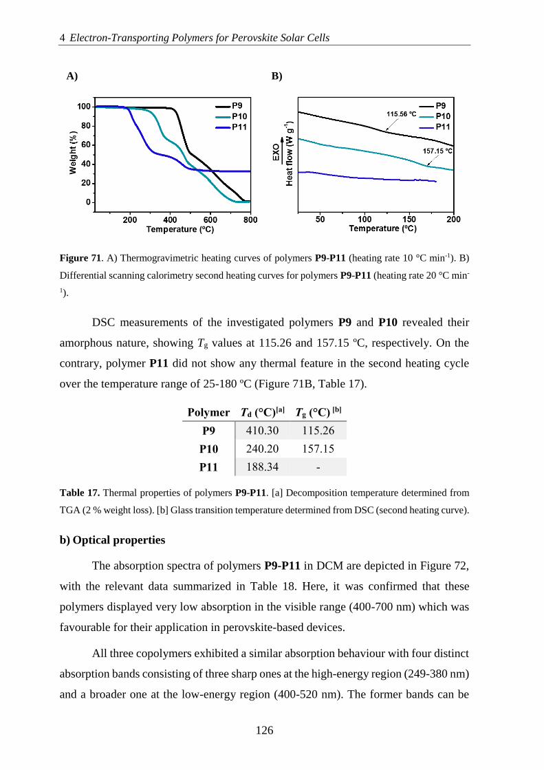
4 Electron-Transporting Polymers for Perovskite Solar Cells
126
A)
B)
Figure 71. A) Thermogravimetric heating curves of polymers P9-P11 (heating rate 10 °C min-1). B)
Differential scanning calorimetry second heating curves for polymers P9-P11 (heating rate 20 °C min-
1).
DSC measurements of the investigated polymers P9 and P10 revealed their
amorphous nature, showing Tg values at 115.26 and 157.15 ºC, respectively. On the
contrary, polymer P11 did not show any thermal feature in the second heating cycle
over the temperature range of 25-180 ºC (Figure 71B, Table 17).
Polymer Td (°C)[a] Tg (°C) [b]
P9 410.30 115.26
P10 240.20 157.15
P11 188.34 -
Table 17. Thermal properties of polymers P9-P11. [a] Decomposition temperature determined from
TGA (2 % weight loss). [b] Glass transition temperature determined from DSC (second heating curve).
b) Optical properties
The absorption spectra of polymers P9-P11 in DCM are depicted in Figure 72,
with the relevant data summarized in Table 18. Here, it was confirmed that these
polymers displayed very low absorption in the visible range (400-700 nm) which was
favourable for their application in perovskite-based devices.
All three copolymers exhibited a similar absorption behaviour with four distinct
absorption bands consisting of three sharp ones at the high-energy region (249-380 nm)
and a broader one at the low-energy region (400-520 nm). The former bands can be

4.3 Results and Discussion
127
assigned to π-π* transitions of the backbones while the latter are related to a charge
transfer process.
The absorption band centred in between 249 and 253 nm could be assigned to
π- π* transitions of the benzene unit. This band was the most intense with Ɛ values at
42996, 52204 and 48462 M-1 cm-1, for polymers P9, P10 and P11, respectively. The
other two absorption bands at the high-energy region with a maximum at 359 and 379
nm (378 nm for P10) are characteristics of π- π* transitions of the NDI core, similar to
those presented in model compounds MC1-MC3. Finally, the polymers exhibited a
long-wavelength absorption band with maximum values at 438, 444 and 447 nm, for
P9, P10 and P11, respectively. This band, which was relatively less intense than the
other three could be attributed to an intramolecular charge transfer (ICT) between the
electron donor (benzene) and the NDI electron-deficient unit, which was in accordance
with previously reported NDI-donor copolymers.[267–270] The ICT absorption peak of
the ammonium-functionalized copolymer P11 was slightly red-shifted compared with
that of polymer P9 and P10, which could be due to the electrostatic perturbation by
ions in close proximity to the optically segment, solvatochromic effects arising from
the polar solvent, or multichain aggregation.[251]
Figure 72.Absorption spectra of polymers P9-P11 in DCM.
The Eg values of polymers P9, P10 and P11 were estimated to be 2.44, 2.41 and
2.35 eV, respectively, according to their λonset values at 508, 514 and 528 nm (Table
18).

4 Electron-Transporting Polymers for Perovskite Solar Cells
128
Polymer λabs (nm) Ɛ (M-1cm-1) λonset (nm) Eg (eV)
P9
253 42996
508 2.44 359 16860
379 18336
438 5238
P10
251 52204
514 2.41 359 19580
378 22413
444 5640
P11
249 48462
528 2.35 359 15260
379 17478
447 4229
Table 18. Optical properties of polymers P9-P11.
c) Electrochemical properties
The electrochemical characterization of NDI-based polymers P9-P11 was
carried out by CV measured in a 0.1 M solution of TBAHFP in anhydrous DCM. The
voltammograms illustrate that all compounds are highly electron-deficient, consistent
with the presence of the NDI moiety (Figure 73).
Their ELUMO values (Table 19) were calculated according to equation 20, as it
was explained for model compounds MC1-MC3.
As for model compounds MC1-MC3, polymers P9-P11 showed two reversible
reduction processes, due to the NDI core (Figure 73). The ELUMO values for P9, P10
and P11 were estimated to be -3.88, -3.80 and -4.03 eV, respectively, according to their
EonsetRed1 values at - 0.92, -1.0 and -0.77 V vs Fc/Fc+, respectively. The ELUMO value of
polymer P11 was lower than those of polymers P9 and P10, which could be explained
due to anion π-interactions between the NDI and the iodine anions, as it occurred in
MC3. Moreover, polymer P11 suffered two non-reversible oxidation processes, while
polymer P10 did not exhibit any oxidation (Figure 73B). This effect may be explained
due to the existence of an electron transfer process from the nitrogen to the NDI core
on polymer P10, as it was above mentioned.

4.3 Results and Discussion
129
With these ELUMO values, these novel NDI-based polymers are perfect
candidates to act as suitable ETMs in PSCs using triple cation perovskite (Figure 73C).
A)
B)
C)
Figure 73. Cyclic voltammograms of A) polymer P9 and B) polymers P10-P11 in DCM /TBAHFP
(0.1 M) at a scan rate of 100 mV s-1. C) Energetic levels of polymers P9-P11 and triple cation
perovskite light absorber used in photovoltaic studies performed in chapters 2 and 3.
Moreover, the EHOMO levels were estimated from the difference between ELUMO
and Eg of the polymers as -6.32, -6.21 and -6.38 eV for P9, P10 and P11, respectively
(Table 19). These low-lying EHOMO levels indicate that the three polymers possess hole-
blocking properties. Thus, these materials can behave as suitable filters towards
electrons, while efficiently blocking holes, which is of primary importance in order to
design innovative ETMs for PSCs.
Polymer E1/2Red1(V) E1/2
Red2(V) EonsetRed1 (V) EHOMO (eV) ELUMO (eV)
P9 -1.36 -1.68 -0.92 -6.32 -3.88
P10 -1.27 -1.72 -1.00 -6.21 -3.80
P11 -1.05 -1.67 -0.77 -6.38 -4.03
Table 19. Electrochemical properties and energy levels of polymers P9-P11.

4 Electron-Transporting Polymers for Perovskite Solar Cells
130
4.4 Conclusions
In summary, three novel n-type NDI-based polymers (P9-P11) were designed,
synthesized and fully characterized. The novel polymers meet the requirements to be used as
ETMs in PSCs. In particular, the polymers showed suitable energy levels with low-lying
LUMO levels of about -4 eV and HOMO levels around -6 eV, which would ensure electron
extraction from the perovskite and hole-blocking functionality, respectively. Moreover,
thermal analysis indicated that polymers were thermally stable with no phase transition under
operation temperature of PSCs. All of them possessed good solubility providing a facile way
to process ETLs.
Furthermore, three NDI-based small molecules (MC1-MC3), with similar structure to
the NDI unit of the backbone of polymers P9-P11, were synthesized and fully characterized.
The charge transporting properties of those small molecules were studied by FP-TRMC to
estimate their pseudo-photoconductivity. Both the amino and iodine-quaternized ammonium
groups in molecules MC2 and MC3 exhibited higher pseudo-conductivity compared to
molecule MC1.
Polymers P9-P11 display the same structural amino or ammonium fragments than
model compounds MC1-MC3. Thus, in principle we could expect good charge transporting
properties for these innovative polymers in addition to their excellent ETM characteristics. To
confirm this trend, we are currently collaborating with Prof. Seki at Kyoto University (Japan)
as well as working on the optimization of OFETs of MC1-MC3 and P9-P11.
The next logical step would be the incorporation of these innovative NDI-based
polymers as ETMs in PSCs. However, taking into account the amount of polymer necessary
to carry out a complete photovoltaic study, the study on their charge transporting properties is
of primary importance to guarantee a successful incorporation of these compounds in devices
based on triple cation perovskites.

5. EXPERIMENTAL SECTION


5.1 General Methods and Materials
133
5 EXPERIMENTAL SECTION
5.1 General Methods and Materials
All commercially available reagents and solvents were used as received without
further purification. Anhydrous solvent was dried using a SPS purification system.
Column chromatography was carried out using silica gel (40 to 60 µm, 60 Å) as
stationary phase. Thin layer chromatography (TLC) was performed on precoated silica
gel and observed under UV light.
5.1.1 Nuclear Magnetic Resonance Spectroscopy
The 1H NMR, 13C NMR and 19F NMR spectra were taken on Bruker NMR
spectrometers (300 MHz, 400 MHz and 500 MHz for 1H NMR, 75 MHz, 100 MHz and
125 Hz for 13C NMR and 376 MHz for 19F NMR) at room temperature.
Coupling constants (J) are denoted in Hz and chemical shifts (δ) in ppm.
Abbreviations of coupling patterns are as follows: s = singlet, d = doublet, t = triplet,
m = multiplet, dd = doublet of doublets, td = triplet of doublets. The abbreviation used
for indicating a quaternary C-atom is q.
5.1.2 Mass Spectrometry
MALDI-TOF: Matrix Assisted Laser Desorption Ionization (MALDI)
experiments, coupled to a Time-of-flight (TOF) analyzer, were recorded on Bruker
REFLEX spectrometer.
ESI-TOF: Electrospray ionization (ESI) measurements were carried out on
HPLC Agilent 1200 Series system coupled to a hybrid quadrupole-time of flight (LC-
QTOF) mass spectrometer Agilent 6520 from Agilent Technologies (Santa Clara, CA,
USA).

5 Experimental Section
134
5.1.3 Size Exclusion Chromatography
The molecular weight distribution of the polymers was determined by size
exclusion chromatography (SEC, Waters). The setting consisted of a pump, a
differential refractometer (Waters 2410) and three columns in series (Styragel HR2,
HR4 and HR6; with a pore size from 102 to 106 Å). The analysis were performed at 35
ºC and THF was used as solvent at a flow rate of 1 mL min-1. Calibration was relative
to polystyrene standards. A series of polystyrene standards in the range of 580-
3,848,000 g mol-1 were used to prepare a universal calibration curve.
5.1.4 Water Contact Angle Measurements
Water contact angles were measured in an OCA 20 instrument (Dataphysics).
For contact angle measurements, distilled water droplets of 10 μL were placed on the
surface of the films. The values given are an average of five measurements per film.
5.1.5 Thermal Analysis
The thermogravimetric analysis (TGA) were performed on a TA Q500 using a
10 °C min-1 heating rate under a nitrogen flow.
Differential scanning calorimetry (DSC) was performed on a DSC3+ Mettler
Toledo at a scan rate of 20 °C min-1 in the nitrogen atmosphere.
5.1.6 Absorption and Fluorescence Spectroscopy
Absorption measurements were recorded on a Perkin-Elmer Lambda 950
spectrometer. All the compounds were measured at various concentrations (10-5-10-7
mol L-1) to affirm linear behaviour. The measurements of films of compounds in
chapter 3 were performed on samples that were spin-coated from the respective solvent
onto a FTO/SnO2 substrates. The optical band gap (Eg) was estimated from the onset
of the absorption edge (λonset) in the longer wavelength region.

5.1 General Methods and Materials
135
Emission measurements were recorded on a LS55 Perkin-Elmer Fluorescence
spectrometer.
5.1.7 Cyclic Voltammetry
Cyclic voltammograms were carried out on a Princeton Applied Research
Parstat 2273 in a 3-electrode single compartment cell with platinum disc working
electrode, a platinum wire counter electrode and a silver wire pseudoreference
electrode. For electrochemical measurements of polymers P9-P11 a glassy carbon disc
working electrode was used instead of using the platinum disc working electrode. All
the potential values were reported versus the redox potential of the
ferrocene/ferrocenium redox couple.
EHOMO and ELUMO values were obtained from the onset potentials of cyclic
voltammetry measurements. The potential of Fc/Fc+ is 0.2 V vs. the normal hydrogen
electrode (NHE), which has an absolute potential of -4.6 eV vs. vacuum.[271] Therefore,
the energy levels are EHOMO/LUMO (eV) = -4.8 – EonsetOx1/Red1
(as it was shown in equations
17 and 20) and the optical band gap Eg = ELUMO – EHOMO.
5.1.8 Time-Resolved Microwave Conductivity
Time resolved microwave conductivity (TRMC) experiments were conducted
for the sample on a quartz plate using a third harmonic generator (THG; 355 nm) of a
Nd:YAG laser (Continuum, Inc., Surelite II, 5-8 ns pulse duration, 10 Hz) as the
excitation source (9.1 × 10¹⁵ photons cm–2 pulse-1). The photoconductivity transient Δσ
was converted to the product of the quantum yield (φ) and the sum of the charge carrier
mobilities, Σμ (μ+ + μ-) by φΣμ = Δσ (eI0Flight)-1, where e and Flight are the unit charge
of a single electron and the correction (or filling) factor, respectively.
5.1.9 Scanning Electron Microscopy
Scanning electron microscopy (SEM) was performed on a ZEISS Merlin HR-
SEM. Scanning Probe Image Processor (SPIP) software was used for processing and

5 Experimental Section
136
analysing the micrographs in order to obtain the mean area and mean diameter showed
in chapter 3.
5.1.10 Atomic Force Microscopy
Atomic force microscopy (AFM) measurements were recorded on a Bruker
Dimension ICON on a tapping mode.
5.1.11 X-Ray Diffraction
X-ray diffraction (XRD) patterns were obtained on a Bruker D8 Advance X-
Ray diffractometer with Cu Kα (λ = 1.5418 Å) radiation.
5.2 Synthesis
5.2.1 Dopant-Free Hole-Transporting Polymers for PSCs
Synthesis of Precursors 1-8
Synthesis of 3,4-bis(2-ethylhexyl)-thiophene (1)[272]
A procedure reported in the literature was adapted with some modifications. 2-
Ethylhexyl bromide (2.95 mL, 16.5 mmol) dissolved in 5 mL of anhydrous diethyl
ether (Et2O) was added to a solution of magnesium turnings (602 mg, 24.8 mmol) in 5
mL of anhydrous Et2O, containing one crystal of iodine, over a period of 30 min. After
complete addition, the mixture was ultrasonicated at 40 °C under a nitrogen atmosphere
for a further hour. The obtained (Grignard) solution was slowly added to a mixture of
3,4-dibromothiophene (1.00 g, 4.13 mmol), Ni(dppp)Cl2 (65.0 mg, 120 μmol) in 10
mL of anhydrous Et2O at 0 °C, together with 10 mL of Et2O (to transfer the Grignard
reagent completely). The reaction mixture was stirred for 16 h at room temperature
under nitrogen atmosphere. Afterwards, an aqueous solution of HCl (1 M, 50.0 mL)

5.2 Synthesis
137
was added to the solution, which was previously chilled to 0 °C. The phases were
separated and the aqueous phase was extracted with Et2O (3 x 50 mL) .The combined
organic phases were washed with water (2 x 100 mL) and finally with brine (1 x 100
mL). The organic phase was dried over Na2SO4, concentrated under reduced pressure
and the resulting yellowish oil was purified by flash column chromatography using
hexane as eluent to give compound 1 as colourless oil (959 mg, 76%). It was used
directly in the next step without further purification.
1H NMR (300 MHz, CDCl3), δ (ppm): 6.85 (s, 2H, Ha), 2.44 (d, J = 7.1 Hz, 4H,
Hb), 1.61-1.51 (2H, Hc), 1.41-1.17 (16H, Hd-f + Hh), 0.94-0.80 (12H, Hg + Hi).
Synthesis of 1-(2-ethylhexyloxy)-4-iodobenzene (2)[161]
K2CO3 (3.86 g, 27.9 mmol) was added to a solution of 4-iodophenol (4.00 g,
18.2 mmol) and 2-ethylhexyl bromide (3.90 mL, 21.8 mmol) in 20 mL of DMF. The
reaction mixture was stirred for 6 h at 130 °C. After cooling down, the suspension was
filtered and the solvent removed under vacuum. The resulting residue was diluted with
DCM (40 mL) and washed with water (3x 40 mL) and brine (1 x 40 mL). The organic
phase was dried over anhydrous Na2SO4, concentrated under reduced pressure and
purified by flash column chromatography using hexane as eluent yielding the target
product as a colourless oil (5.00 g, 83%).
1H NMR (300 MHz, CD2Cl2), δ (ppm): 7.58-7.51 (m, 2H, Ha), 6.72-6.68 (m, 2H, Hb),
3.81 (d, J = 5.7 Hz, 2H, Hc), 1.76-1.64 (m, 1H, Hd), 1.56-1.26 (8H, He-g + Hi), 0.95-0.84 (6H,
Hh + Hj).
Synthesis of 4-(2-ethylhexyloxy)-N,N-diphenylaniline (3)[162]

5 Experimental Section
138
A procedure reported in the literature was adapted with some modifications.[162]
1-(2-Ethylhexyloxy)-4-iodobenzene (2, 1.50 g, 4.52 mmol) was introduced into a
Schlenk flask, and three cycles of nitrogen-vacuum were then applied. Next, sodium
tert-butoxide (1.18 g, 12.3 mmol), Pd2(dba)3 (37.5 mg, 0.04 mmol), tri-tert-butyl
phosphine (1M in toluene, 410 μL, 410 μmol) and anhydrous toluene (25 mL) were
added. After purged with nitrogen for 30 min, diphenylamine (696 mg, 4.11 mmol)
was added and the mixture was stirred at 120 °C for 15 h. Afterwards, the reaction was
allowed to cool down and 40 mL of water and 40 mL of chloroform were added. The
aqueous phase was extracted with chloroform (2 x 40 mL) and the combined organic
phases were washed with water (2 x 150 mL) and brine (1 x 150 mL). The organic
phase was dried over anhydrous Na2SO4, concentrated under reduced pressure and
purified by flash column chromatography using hexane:toluene (5:1) as eluent to afford
3 as a white solid (1.33 g, 87%).
1H NMR (300 MHz, CD2Cl2), δ (ppm): 7.28-7.21 (4H, Hb), 7.11-7.04 (6H, Hc
+ Hd), 7.00-6.95 (2H, Ha), 6.92-6.87 (2H, He), 3.89 (d, J = 5.7 Hz, 2H, Hf), 1.84-1.72
(1H, Hg), 1.65-1.36 (8H, Hh-j + Hl), 1.02-0.91 (6H, Hk + Hm).
Synthesis of triarylamine 4[163]
4-(2-Ethylhexyloxy)-N,N-diphenylaniline (3, 0.53 g, 1.42 mmol) was dissolved
in 12 mL of a mixture of chloroform/AcOH (5:1) and degassed for 30 min with a
nitrogen stream. After cooling the solution to -10 °C, NBS (250 mg, 2.98 mmol) was
added in small portions under exclusion of light. The reaction mixture was stirred for
3.5 h at -10 °C and quenched with NaOH (1 M, 50 mL). The aqueous phase was
extracted with DCM (2 x 50 mL) and the organic phase was washed with water (2 x
100 mL) and brine (1 x 100 mL), dried over anhydrous Na2SO4 and concentrated under
reduced pressure. The resulting residue was purified through flash column

5.2 Synthesis
139
chromatography using petroleum ether (PE):DCM (10:1) as eluent to afford
triarylamine 4 as a dark orange oil (660 mg, 87%).
1H NMR (300 MHz, CD2Cl2), δ (ppm): 7.35-7.29 (m, 4H, Ha), 7.05-6.99 (m,
2H, Hc), 6.92-6.83 (m, 6H, Hb + Hd), 3.84 (d, J = 5.7 Hz, 2H, He), 178-1.66 (m, 1H,
Hf), 1.56-1.30 (8H, Hg-i + Hk), 0.96-0.85 (6H, Hj + Hl).
Synthesis of triarylamine 5[273]
A procedure reported in the literature was adapted with some modifications.[273]
1-(2-Ethylhexyloxy)-4-iodobenzene (2, 1.00 g, 3.01 mmol) was introduced into a
Schlenk flask and three cycles of argon-vacuum were applied. Next, 4-bromoaniline
(172 mg, 1.00 mmol), KOH (651mg, 11.6 mmol) and anhydrous toluene (10 mL) were
added and the flask was purged with argon for 30 min. Upon addition of copper (I)
iodide (12.5 mg, 0.07 mmol) and 1,10-phenantroline (11.9 mg, 66.0 μmol) the mixture
was refluxed for 20 h. Afterwards, the reaction was allowed to cool and the crude
product was dissolved in 20 mL of DCM and washed with 20 mL of HCl (1 M). The
aqueous phase was extracted with DCM (2 x 20 mL) and the combined organic phases
were washed with brine (1 x 40 mL). The organic phase was dried over anhydrous
Na2SO4, concentrated under reduced pressure and purified by flash column
chromatography using PE:DCM (20:1→10:1) as eluent to afford 5 as an orangish solid
(0.46 g, 80%).
1H NMR (300 MHz, CD2Cl2), δ (ppm): 7.26-7.19 (m, 2H, Ha), 7.01 (d, J = 8.7
Hz, 4H, Hd), 6.87-6.80 (m, 4H, Hc), 6.75 (d, J = 8.7 Hz, 2H, Hb), 3.82 (d, J = 5.7 Hz,
4H, He), 1.77-1.64 (m, 2H, Hf) , 1.55-1.27 (16H, Hg-i + Hk), 1.00-0.81 (12H, Hj + Hl).

5 Experimental Section
140
Synthesis of triarylamine 6
Compound 5 (2.20 g, 3.79 mmol) was added to a Schlenk flask and three cycles
of argon-vacuum were then applied. Next tri-tert-butyl phosphine (1 M in toluene, 400
μL, 400 μmol) and sodium tert-butoxide (1.09 g, 11.4 mmol) were dissolved in dry
toluene (18 mL) degassed with argon for 30 min. Upon addition of Pd2(dba)3 (36.9 g,
40.3 μmol), diphenylamine (614 mg, 3.79 mmol) was added and the mixture was
refluxed over-night. Afterwards, the reaction was allowed to cool down and 20 mL of
water and 20 mL of DCM were added to the crude product. The aqueous phase was
extracted with DCM (2 x 20 mL) and the combined organic phases were washed with
brine (1 x 40 mL). The organic phase was dried over anhydrous Na2SO4, concentrated
under reduced pressure and purified by flash column chromatography using PE:DCM
(10:1) as eluent to afford 6 as an orange-yellowish solid (2.17 g, 86%).
1H NMR [300 MHz, (CD3)2CO)], δ (ppm): 7.29-7.21 (4H, Hb), 7.08-6.83 (18H,
Ha + Hc + Hd-g), 3.89 (d, J = 5.6 Hz, 4H, Hh), 1.80-1.68 (m, 2H, Hi), 1.61-1.32 (16H,
Hj-l + Hn), 1.02-0.88 (12H, Hm + Ho).
13C NMR [(75 MHz, (CD3)2CO)], δ (ppm): 156.54 (q), 148.99 (q), 145.90 (q),
141.82 (q), 141.47 (q), 130.03 (CH), 127.10 (CH), 127.02 (CH), 123.86 (CH), 122.92
(CH), 122.66 (CH), 116.18 (CH), 71.25 (CH2), 40.34 (CH), 31.32 (CH2), 29.82 (CH2,
overlapping with the solvent signal), 24.60 (CH2), 23.73 (CH2), 14.37 (CH3), 11.46
(CH3).
MS (MALDI-TOF): calculated for C46H56N2O2 [M]+: 668.434, found: 668.403.

5.2 Synthesis
141
Synthesis of bis(4-bromophenyl)amine (7)[165]
A solution of NBS (4.20 g, 23.6 mmol) in 20 mL of DMF was added dropwise
to an ice-cooled solution of diphenylamine (2.00 g, 11.8 mmol) in 20 mL of DMF.
Next, the mixture was stirred for 24 h at room temperature. Afterwards, 40 mL of water
were added, and the precipitate was filtered and dried under vacuum affording the
target product as a white solid (2.45 g, 63%).
1H NMR (300 MHz, CDCl3), δ (ppm): 7.40-7.32 (m, 4H, Hb), 6.96-6.89 (m, 4H,
Ha), 6.04-5.34 (1H, NH).
Synthesis of triarylamine 8[166]
4-Iodoanisole (690 mg, 2.95 mmol) was added to a Schlenk flask and three
cycles of argon-vacuum were then applied. Next, KOH (1.61 g, 28.7 mmol) and dry
toluene (15 mL) were added. Afterwards, the reaction mixture was degassed with a
stream of argon for 10 min before and after 1,10-phenanthroline (28.8 mg, 160 μmol)
and copper (I) iodide (30.5 mg, 160 μmol) were added. Then, bis(4-
bromophenyl)amine (7, 800 mg, 2.46 mmol) was added and the mixture was refluxed
for 20 h. Afterwards, 20 mL of DCM and 20 mL of HCl (1 M) were added and the
phases were separated. The aqueous phase was extracted with DCM (2 x 20 mL) and
the combined organic phases were washed with water (2 x 40 mL) and brine (1 x 40
mL). The organic phase was dried over anhydrous Na2SO4, concentrated under reduced
pressure and purified by flash column chromatography using PE:DCM (4:1→1:3) as
eluent to give the product as a white solid (710 mg, 67%).
1H NMR [(300 MHz, (CD3)2CO)], δ (ppm): 7.45-7.33 (m, 4H, Hd), 7.12-7.05
(m, 2H, Ha), 7.00-6.87 (6H, Hb + Hc), 3.81 (s, 3H, O-CH3).

5 Experimental Section
142
Synthesis of Monomers M1-M5
Synthesis of monomer M1
4,4′-di-tert-butyl-2,2′-bipyridine (48.3 mg, 180 μmol) and bis
(pinacolato)diboron (1.88 g, 7.39 mmol) were added, subsequently, to a 100 mL two-
neck flask containing 3,4-bis(2-ethylhexyl)-thiophene (1, 1.90 g, 6.16 mmol), under
nitrogen atmosphere. After three cycles of nitrogen-vacuum, 25 mL of degassed
heptane were injected into the flask together with. [Ir(OMe)(COD)]2 (58.8 mg, 88.7
μmol). The reaction mixture was stirred at 50 °C for 16 h under nitrogen atmosphere.
After cooling down to room temperature, the mixture was filtered and washed with hot
hexane. The filtrated was concentrated, and the crude product was purified by flash
column chromatography, eluting with ethyl acetate (AcOEt):hexane (5:95) to give a
colourless oil (1.92 g, 56%).
1H NMR (300 MHz, CDCl3), δ (ppm): 2.74 (d, J = 7.3 Hz, 4H, Hb), 1.52-1.43
(2H, Hc), 1.35-1.15 (40H, Ha + Hd-f + Hh), 0.91-0.79 (12H, Hg + Hi).
13C NMR (75 MHz, CDCl3), δ (ppm): 153.48 (q), 83.65 (q), 41.58 (CH), 33.33
(CH2), 32.72 (CH2), 29.28 (CH2), 25.75 (CH2), 24.93 (CH3), 23.36 (CH2), 14.33 (CH3),
11.21 (CH3).
MS (MALDI-TOF, LDI): calculated for C32H58B2NaO4S [M+Na]+: 583.414,
found: 583.398.

5.2 Synthesis
143
Synthesis of monomer M2[274]
Compound 4 (250 mg, 471 μmol), bis (pinacolato)diboron (350 mg, 1.39 mmol)
and potassium acetate (360 mg, 3.70 mmol) were dissolved in 5 mL of anhydrous 1,4-
dioxane. The resulting suspension was degassed with a nitrogen stream before and after
the addition of PdCl2(dppf) (10.1 mg, 13.9 µmol). This mixture was stirred at 80 °C for
15 h under nitrogen atmosphere. After cooling down to room temperature, 40 mL of
water was added, and the aqueous phase was extracted with DCM (2 x 40 mL). The
combined organic phases were washed with water (2 x 150 mL), brine (1 x 150 mL)
and then dried over anhydrous Na2SO4, concentrated under reduced pressure and
purified by flash column chromatography using PE:AcOEt (20:1) as eluent. The
residue was further purified by crystallization in MeOH to afford M2 as a white solid
(0.12 g, 42%).
1H NMR (300 MHz, CD2Cl2), δ (ppm): 7.65-7.51 (4H, Ha), 7.10-6.95 (6H, Hb
+ Hc), 6.91-6.83 (2H, Hd), 3.84 (d, J = 5.7 Hz, 2H, He), 1.79-1.64 (m, 1H, Hf), 1.55-
1.27 (32H, Hg-i + Hk + Hm), 0.98-0.83 (6H, Hj + Hl).
13C NMR (75 MHz, CD2Cl2), δ (ppm): 157.48 (q), 150.91 (q), 140.03 (q),
136.27 (CH), 128.78 (CH), 122.16 (CH), 116.05 (CH), 84.13 (q) 71.36 (CH2), 40.05
(CH), 31.13 (CH2), 29.70 (CH2), 25.26 (CH3), 24.48 (CH2), 23.67 (CH2), 14.47 (CH3),
11.52 (CH3).
MS (MALDI-TOF): calculated for C38H53B2NO5 [M]+: 625.411, found:
625.440.

5 Experimental Section
144
Synthesis of monomer M3
Compound 6 (730 mg, 1.08 mmol) was dissolved in 15 mL of DMF and the
solution was degassed for 30 min with an argon stream. After cooling down the solution
to 0 °C, NBS (410 mg, 2.27 mmol) was added in small portions under exclusion of
light. Next, the reaction mixture was allowed to stir for 24 h at room temperature.
Afterwards, the solvent was removed under reduced pressure and 20 mL of DCM and
20 mL of water were added. The phases were separated and the aqueous phase was
extracted with DCM (2 x 20 mL). The combined organic phases were washed with
water (2 x 50 mL) and brine (1 x 50 mL), dried over Na2SO4, filtered and the solvent
removed under reduced pressure. The residue was purified by flash column
chromatography using PE:DCM (30:1→10:2) as eluent to afford M3 as an oil (0.54,
60%).
1H NMR [(300 MHz, (CD3)2CO)], δ (ppm): 7.43-7.33 (m, 4H, Hb), 7.08-6.81
(16H, Ha + Hc-f), 3.87 (d, J = 5.6 Hz, 4H, Hg), 1.17-1.65 (2H, Hh), 1.59-1.27 (16H, Hi-
k + Hm), 0.98-0.85 (12H, Hl + Hn).
13C NMR [(75 MHz, (CD3)2CO)], δ (ppm): 157.23 (q), 148.27 (q), 147.33 (q),
141.90 (q), 140.28 (q), 133.47 (CH), 128.10 (CH), 127.84 (CH), 125.76 (CH), 122.50
(CH), 116.67 (CH), 115.40 (q), 71.46 (CH2), 40.53 (CH), 31.52 (CH2), 30.05 (CH2,
overlapping with the solvent signal), 24.81 (CH2), 23.94 (CH2), 14.58 (CH3), 11.68
(CH3).
MS (MALDI-TOF): calculated for C46H54Br2N2O2 [M]+: 824.255, found:
824.399.

5.2 Synthesis
145
Synthesis of monomer M4[164]
2,7-Dibromo-9,9'-spirobifluorene (200 mg, 422 μmol), bis (pinacolato)diboron
(320 mg, 1.27 mmol) and potassium acetate (330 mg, 3.38 mmol) were dissolved in 8
mL of anhydrous 1,4-dioxane. The resulting suspension was degassed with an argon
stream before and after PdCl2(dppf) (9.50 mg, 12.9 μmol) was added and the mixture
was stirred at 80 °C for 15 h under argon atmosphere. After cooling down to room
temperature, the residue was dissolved in 40 mL of water and 40 mL of DCM and the
phases were separated. The aqueous phase was extracted with DCM (2 x 40 mL) and
the combined organic phases were washed with water (2 x 80 mL) and brine (1 x 80
mL). Finally, the resulting organic phase was dried over anhydrous Na2SO4,
concentrated under reduced pressure and purified by flash column chromatography
using hexane:AcOEt (9:1) as eluent to afford M4 as a white solid (0.16 g, 66%).
1H NMR (300 MHz, CD2Cl2), δ (ppm): 7.92 (d, J = 7.6 Hz, 4H, Ha + Hg), 7.82
(dd, J = 0.9 Hz, 7.6 Hz, 2H, Hf), 7.42 (td, J = 1.0 Hz, 7.5 Hz, 2H, Hb), 7.14 (td, J = 1.0
Hz, 7.6 Hz, 2H, Hc), 7.04 (s, 2 H, He), 6.67 (d, J = 7.6 Hz, 2H, Hd), 1.23 (s, 24H, Hh).
Synthesis of monomer M5[166]
Compound 8 (1.07 g, 2.47 mmol), bis (pinacolato)diboron (1.88 g, 7.41 mmol)
and potassium acetate (1.94 g, 19.8 mmol) were dissolved in 20 mL of anhydrous 1,4-
dioxane. The resulting suspension was degassed with a nitrogen stream before and after
PdCl2(dppf) (51.1 mg, 69.9 μmol) was added, and the mixture was stirred at 80 °C for
15 h under nitrogen atmosphere. After cooling down to room temperature, water (20

5 Experimental Section
146
mL) was added and the aqueous phase was extracted with DCM (3 x 30 mL). The
combined organic phases were washed with water (2 x 60 mL), brine (1 x 60 mL) and
dried over anhydrous Na2SO4, concentrated under reduced pressure and purified by
flash column chromatography using hexane:AcOEt (9:1) as eluent. The residue was
further purified by crystallization in EtOH to give monomer M5 as a white solid (680
mg, 44%).
1H NMR [(300 MHz, (CD3)2CO)], δ (ppm): 7.66-7.59 (m, 4H, Hd), 7.12-7.04
(m, 2H, Ha), 7.02-6.93 (6H, Hb + Hc), 3.82 (s, 3H, O-CH3), 1.32 (s, 24H, He).
Synthesis of Polymers P1-P6
Synthesis of polymer P1
Monomer M1 (368 mg, 657 µmol) was added to a Schlenk flask under nitrogen.
Next, anhydrous toluene (16 mL) and aq. NaHCO3 (0.2 M. 5.98 mL, 1.20 mmol) were
injected together with 2,7-dibromo-9,9'-spirobifluorene (312 mg, 657 µmol) and
Aliquat 336 (56.8 mg) under nitrogen atmosphere. The reaction mixture was degassed
by bubbling nitrogen for 30 min before and after Pd(PPh3)4 (11.4 mg, 9.86 µmol) was
added, and the mixture was stirred vigorously and refluxed for 135 h. Afterwards, 30
mL of chloroform and 30 mL of water were added and upon separation of the phases,
the organic phase was washed with 50 mL of brine. Next, the solvent was removed
under reduced pressure and the resulting residue was dissolved in 4 mL of chloroform
and dripped into 150 mL of cold MeOH. The green precipitate was filtered off and
washed consecutively with MeOH (3 d), hexane (7 d) and acetone (1 d) using a Soxhlet
extractor to afford polymer P1 (319 mg, 78%). SEC: Mn = 9651, Mw = 21635, PDI =
2.2.

5.2 Synthesis
147
1H NMR (300 MHz, CDCl3), δ (ppm): 7.87-7.70 (4H, Ha + Hg), 7.40-7.24 (4H,
Hf + Hb), 7.12-6.99 (2H, Hc), 6.77-6.65 (4H, He + Hd), 2.42-2.14 (4H, Hh), 1.22-1.10
(2H, Hi), 1.10-0.78 (16H, CH2), 0.76-0.65 (6H, CH3), 0.51-0.36 (6H, CH3).
MS (MALDI-TOF): The detection of the building block (C45H48S [M]+:
620.347) of P1 was demonstrated:
Figure 74. MALDI-TOF spectrum of polymer P1.
Synthesis of polymer P2
Monomer M2 (358 mg, 571 µmol) was added to a Schlenk flask under nitrogen.
Next, anhydrous toluene (14 mL) and aq. NaHCO3 (0.2 M. 5.20 mL, 1.04 mmol) were
injected together with 2,7-dibromo-9,9'-spirobifluorene (271 mg, 571 µmol) and
Aliquat 336 (60.9 mg) under nitrogen atmosphere. The reaction mixture was purged
with nitrogen for 30 min before and after Pd(PPh3)4 (9.90 mg, 8.57 µmol) was added.
The mixture was stirred vigorously and refluxed for 135 h and 30 mL of chloroform
and 30 mL of water were added afterwards. After separation of the phases, the aqueous
phase was extracted with chloroform (1 x 30 mL) and the combined organic phases
were washed with 50 mL of brine, dried over anhydrous Na2SO4 and concentrated

5 Experimental Section
148
under reduced pressure. The residue was dissolved in 4 mL of chloroform and dripped
into 150 mL of cold MeOH. The green precipitate was filtered off and washed
consecutively with MeOH (3 d), hexane (4 d) and acetone (2 d) using a Soxhlet
extractor to afford polymer P2 (322 mg, 82%). SEC: Mn = 5551, Mw = 11390, PDI =
2.1.
1H NMR (300 MHz, CD2Cl2), δ (ppm): 7.99-7.76 (4H, Ha + Hg), 7.66-7.48 (2H,
Hf), 7.45-6.81 (16H, Hb,c + Hh-k), 6.81-6.67 (4H, He + Hd), 3.86-3.71 (2H, Hl), 1.77-
1.62 (1H, Hm), 1.56-1.22 (8H, Hn-p + Hr), 1.01-0.80 (6H, Hq + Hs).
MS (MALDI-TOF): The detection of the building block (C51H43NO [M]+:
685.322) of P2 was demonstrated (Figure 28).
Synthesis of polymer P3
The dibrominated monomer M3 (446 mg, 539 µmol) was added to a Schlenk
flask under nitrogen. Next, anhydrous toluene (13 mL) and aq. NaHCO3 (0.2 M, 4.90
mL, 981 µmol) were injected together with monomer M1 (301 mg, 539 µmol) and
Aliquat 336 (45.0 mg) under nitrogen atmosphere. The reaction mixture was purged
with nitrogen for 30 min before and after Pd(PPh3)4 (9.34 mg, 8.09 µmol) was added.
The mixture was stirred vigorously and refluxed for 135 h and 30 mL of DCM and 30
mL of water were added afterwards. The aqueous phase was extracted with DCM (1 x
30 mL) and the combined organic phases were washed with 50 mL of brine, dried over
anhydrous Na2SO4 and concentrated under reduced pressure. The residue was
dissolved in 4 mL of DCM and dripped into 150 mL of cold MeOH. The green

5.2 Synthesis
149
precipitate was filtered off and washed consecutively with MeOH (4 d), CH3CN (2 d)
and acetone (7 d) using a Soxhlet extractor to afford polymer P3 (160 mg, 31%). SEC:
Mn = 3209, Mw = 4746, PDI = 1.5.
1H NMR (300 MHz, CD2Cl2), δ (ppm): 7.52-6.78 (20H, HAr), 3.86-3.77 (4H,
Hc), 2.69-2.56 (4H, Hb), 179-1.64 (2H, Hd), 1.57-1.03 (34H, CH2 + Ha), 0.99-0.64
(24H, CH3).
MS (MALDI-TOF): The detection of the building block (C66H88N2O2S [M]+:
972.656) of P3 was demonstrated:
Figure 75. MALDI-TOF spectrum of polymer P3.
Synthesis of polymer P4

5 Experimental Section
150
The dibrominated monomer M3 (345 g, 417 µmol) was added to a Schlenk flask
under nitrogen. Next, anhydrous toluene (10 mL) and aq. NaHCO3 (0.2 M, 3.79 mL,
758 µmol) were injected together with monomer M4 (237 mg, 417 µmol) and Aliquat
336 (35.0 mg) under nitrogen atmosphere. The reaction mixture was purged with
nitrogen for 30 min before and after Pd(PPh3)4 (7.72 mg, 6.25 µmol) was added. The
mixture was stirred vigorously and refluxed for 135 h. Afterwards, 30 mL of DCM and
30 mL of water were added and the phases were separated. The aqueous phase was
extracted with DCM (1 x 30 mL) and the combined organic phases were washed with
50 mL of brine, dried over anhydrous Na2SO4 and concentrated under reduced pressure.
The residue was dissolved in 4 mL of DCM and dripped into 150 mL of cold MeOH.
The green precipitate was filtered off and washed consecutively with MeOH (5 d),
hexane (2 d) and acetone (4 d) using a Soxhlet extractor to afford polymer P4 (276 mg,
67%). SEC: Mn = 4403, Mw = 10528, PDI = 2.4.
1H NMR (300 MHz, CD2Cl2), δ (ppm): 8.04-6.68 (34H, HAr), 3.87-3.74 (4H,
Hn), 178-1.65 (2H, Ho), 1.55-1.25 (16H, CH2), 1.01-0.81 (12H, CH3).
MS (MALDI-TOF, DCTB): The detection of the building block (C71H69N2O2
[M+H]+: 981.535) of P4 was demonstrated:
Figure 76. MALDI-TOF spectrum of polymer P4.

5.2 Synthesis
151
Synthesis of polymer P5
The dibrominated monomer M3 (306 mg, 370 µmol) was added to a Schlenk
flask under nitrogen. Next, anhydrous toluene (9 mL) and aq. NaHCO3 (0.2 M, 3.37
mL, 673 µmol) were injected together with monomer M5 (231 mg, 370 µmol) and
Aliquat 336 (47.8 mg) under nitrogen atmosphere. The reaction mixture was purged
with argon for 30 min before and after Pd(PPh3)4 (6.42 mg, 5.55 µmol) was added. The
mixture was stirred vigorously and refluxed for 4 d and 30 mL of DCM and 30 mL of
water were added afterwards. The aqueous phase was extracted with 30 mL of DCM
and the combined organic phases were washed with 50 mL of brine, dried over
anhydrous Na2SO4 and concentrated under reduced pressure. The residue was
dissolved in 4 mL of DCM and dripped into 150 mL of cold MeOH. The brown
precipitate was collected by filtration and washed consecutively with MeOH (3 d),
acetone (2 d), hexane (2 d) and MeOH (3 d) using a Soxhlet extractor to afford P5 (176
mg, 46%). SEC: Mn = 4681, Mw = 8663, PDI = 1.9.
1H NMR (300 MHz, CD2Cl2), δ (ppm): 7.66-6.64 (32H, Ha-j), 3.89-3.66 (7H,
OCH3 + Hk), 179-1.61 (2H, Hl), 1.58-1.21 (16H, Hm-o + Hq), 1.01-0.77 (12H, Hp + Hr).
MS (MALDI-TOF): The detection of the building block (C65H69N3O3 [M]+:
939.533) of P5 was demonstrated:

5 Experimental Section
152
Figure 77. MALDI-TOF spectrum of polymer P5.
Synthesis of polymer P6
A mixture of Ni(COD)2 (375 mg, 1.36 mmol), 2,2’-bipyridine (213 mg, 1.36
mmol), 1,5-cyclooctadiene (167 µL, 1.36 mmol), degassed anhydrous toluene (3 mL),
and degassed anhydrous DMF (3 mL) was stirred at room temperature under nitrogen
atmosphere for 30 min. A solution of monomer M3 (470 mg, 568 µmol) in degassed
anhydrous toluene (9.5 ml) and degassed anhydrous DMF (9.5 ml) was added, and the
mixture was stirred at 65 °C for 7 d. The reaction mixture was poured into MeOH:HCl
(20%) (4:1, 500 ml) and stirred for 30 min. The green precipitate was filtered off and
washed consecutively with MeOH (6 d), acetone (2 d) and CH3CN (3 d) using a Soxhlet
extractor to afford polymer P6 (194 mg, 51%). SEC: Mn = 5812, Mw = 12443, PDI =
2.1.

5.2 Synthesis
153
1H NMR (300 MHz, CD2Cl2), δ (ppm): 7.54-7.30 (4H, Hb), 7.18-6.70 (16H, Ha
+ Hc-f), 3.93-3.73 (4H, Hg), 178-1.62 (2H, Hh), 1.57-1.21 (16H, Hi-k + Hm), 1.01-0.81
(12H, Hn + Ho).
MS (MALDI-TOF): The detection of the building block (C46H54N2O2 [M]+:
666.417) of P6 was demonstrated:
Figure 78. MALDI-TOF spectrum of polymer P6.
5.2.2 Perfluorinated Additives for PSCs
Synthesis of Precursors 9 and 10
Synthesis of 1,4-bis(perfluorohexyl)benzene (9)[208]
To a stirred solution of 1,4-diiodobenzene (3.30 g, 10.0 mmol), Cu powder (5.08
g, 80.0 mmol) and 2,2´bipyridine (156 mg, 1.00 mmol) in 30 mL of anhydrous DMSO,
perfluorohexyl iodide (6.50 mL, 30.1 mmol) was added under argon atmosphere. The
resulting mixture was stirred for 72 h at 70 ºC and the reaction was then poured into
200 mL of water:Et2O (1:1) and stirred vigorously for 30 min. After removing the

5 Experimental Section
154
solids by filtration, the organic layer was washed with dilute NH4OH solution (2 x 100
mL), water (2 x 100 mL) and dried over anhydrous Na2SO4. The solvent was removed
under vacuum and the resulting residue was sublimated to give compound 9 as a white
solid (5.92 g, 83%).
1H NMR (400 MHz, CD2Cl2), δ: (ppm) 7.79 (s, 4H).
19F NMR (376 MHz, CD2Cl2), δ: (ppm) -126.4 (4F), -123.0 (4F), -122.0 (4F),
121.6 (4F), -111.4 (4F), -81.14 (6F).
Synthesis of 4-bromo-N,N-bis(4-methoxyphenyl)aniline (10)[209]
4-Iodoanisol (16.5 g, 70.5 mmol), copper (I) iodide (255 mg, 1.34 mmol), 1,10-
phenantroline (241 mg, 1.34 mmol) and KOH (14.7 g, 261 mmol) were dissolved in
previously degassed anhydrous toluene (80 mL). Then, 4-bromoaniline (5.77 g, 33.6
mmol) was added and after degassing for 5 min the reaction mixture was stirred at 80
ºC for 3 d. After cooling down to room temperature, 100 mL of water and 80 mL of
DCM was added and the phases separated. The aqueous phase was extracted with DCM
(2 x 100 mL) and the combined organic phases were washed with water (1 x 200 mL).
The organic phase was dried over anhydrous Na2SO4, concentrated under reduced
pressure and purified by flash column chromatography on silica gel using PE:DCM
(1:1) as eluent to give triarylamine 10 as a white solid (2.98 g, 23%).
1H NMR [300 MHz, (CD3)2CO)], δ (ppm): 7.36-7.30 (m, 2H, Ha), 7.13-7.06 (m,
4H, Hc), 6.99-6.92 (m, 4H, Hd), 6.81-6.75 (m, 2H, Hb), 3.83 (s, 6H, CH3).

5.2 Synthesis
155
Synthesis of Monomers M6-M7 and Intermediate 11
Synthesis of 1,4-dibromo-2,5-bis(perfluorohexyl)benzene (M6)[208]
To a solution of 4-bis(perfluorohexyl)benzene (9, 2.70 g, 3.78 mmol) in 27 mL
of trifluoroacetic acid and 8 mL of H2SO4 (c), NBS (2.01 g, 11.3 mmol) was added.
The latter was added in small portions (335 mg h-1) under stirring over a period of 5 h,
followed by stirring at 60 °C for 48 h. After that time, the reaction mixture was poured
into iced water and the obtained yellow precipitate was collected by filtration and
recrystallized in EtOH to give monomer M6 as a white solid (1.87 g, 57%).
1H NMR (400 MHz, CD2Cl2), δ (ppm): 7.99 (s, 2H).
19F NMR (376 MHz, CD2Cl2), δ (ppm): -126.3 (4F), -122.9 (4F), -121.8 (4F),
119.5 (4F), -107.7 (4F), -81.1 (6F).
Synthesis of monomer M7
Compound M3 (0.67 g, 0.81 mmol), bis(pinacolato)diboron (617 mg, 2.43
mmol) and potassium acetate (635 mg, 6.47 mmol) were dissolved in 15 mL of
anhydrous 1,4-dioxane. The solution was degassed for 15 min with an argon stream
and PdCl2(ddpf) (14.5 mg, 19.8 μmol) was added. The reaction mixture was allowed
to stir for 3 d at 80 ºC. After cooling to room temperature, 40 mL of water and 40 mL
of DCM were added and the phases were separated. The aqueous phase was extracted

5 Experimental Section
156
with DCM (3 x 40 mL) and the combined organic layers were washed with water (2 x
100 mL), brine (1 x 100 mL), dried over anhydrous Na2SO4 and concentrated under
reduced pressure. The crude product was purified by flash column chromatography on
silica gel using hexane:AcOEt (15:1) with 0.5% NEt3 as eluent to give monomer M7
as a white solid (200 mg, 39%).
1H NMR [500 MHz, (CD3)2CO)], δ (ppm): 7.63 (d, J = 8.3 Hz, 4H, Ha), 7.08-
6.84 (16H, Hb-f), 3.87 (d, J = 5.6 Hz, 4H, Hg), 1.76-1.65 (m, 2H, Hh), 1.57-1.23 (40H,
Hi-k + Hm + Ho), 0.97-0.86 (12H, Hl + Hn).
13C NMR [125 MHz, (CD3)2CO)], δ (ppm): 156.96 (q), 151.33 (q). 147.08 (q),
141.71 (q), 140.23 (q), 136.87 (CH), 128.31 (CH), 127.60 (CH), 122.73 (CH), 122.16
(CH), 116.41 (CH), 84.43 (q), 71.40 (CH2), 40.50 (CH), 31.48 (CH2), 29.98 (CH2,
overlapping with the solvent signal), 25.38 (CH3), 24.76 (CH2), 23.90 (CH2), 14.54
(CH3), 11.63 (CH3).
MS (MALDI-TOF): calculated for C58H78B2N2O6 [M]+: 920.600, found
920.595.
Synthesis of intermediate 11[275]
4-Bromo-N,N-bis(4-methoxyphenyl)aniline (10, 1.00 g, 2.60 mmol),
bis(pinacolato)diboron (990 mg, 3.90 mmol) and potassium acetate (2.04 g, 20.8
mmol) were dissolved in 20 mL of anhydrous 1,4-dioxane. The resulting suspension
was degassed with an argon stream before and after PdCl2(dppf) (51.1 mg, 69.8 μmol)
was added and the mixture was stirred at 80 ºC for 48 h under argon atmosphere. After
cooling to room temperature, 40 mL of water and 20 mL of DCM were added and the
phases were separated. The aqueous phase was extracted with DCM (3 x 40 mL) and
the combined organic phases were washed with water (1 x 200 mL) and brine (1 x 200

5.2 Synthesis
157
mL). The organic phase was dried over anhydrous Na2SO4, concentrated under reduced
pressure and purified by flash column chromatography on silica gel using PE:DCM
(1:2) as eluent to give the product as a white solid (0.25 g, 22%).
1H NMR [400 MHz, (CD3)2CO)], δ (ppm): 7.56-7.50 (m, 2H, Ha), 7.12-7.04 (m,
4H, Hc), 6.97-6.88 (m, 4H, Hd), 6.81-6.74 (m, 2H, Hb), 3.80 (s, 6H, CH3), 1.30 (12H,
s, He).
Synthesis of Additives S1, P7 and P8
Synthesis of additive S1
Compound 11 (223 mg, 517 μmol), 1,4-dibromo-2,5-bis(perfluorohexyl)
benzene (M6, 205 mg, 235 mmol), aq. NaHCO3 (0.2 M, 4.70 mL, 0.94 mmol) were
dissolved in 3 mL of anhydrous toluene. The resulting suspension was degassed with
an argon stream before and after Pd(PPh3)4 (37.0 mg, 32.3 μmol) was added and the
mixture was stirred and refluxed for 4 d under argon atmosphere. After cooling to room
temperature, 20 mL of water and 20 mL of DCM were added and the phases separated.
The aqueous phase was extracted with DCM (3 x 20 mL) and the combined organic
phases were washed with water (1 x 80 mL) and brine (1 x 80 mL). The organic phase
was dried over anhydrous Na2SO4, concentrated under reduced pressure and purified
by flash column chromatography on silica gel using toluene (0.5% NEt3) as eluent to
give additive S1 as a yellowish solid (128 mg, 41%).
1H NMR (400 MHz, CDCl3), δ (ppm): 7.58 (s, 2H, He), 7.14-7.03 (12H, Hb +
Hd), 6.94-6.89 (m, 4H, Hc), 6.89-6.82 (m, 8H, Ha), 3.81 (s, 12H, CH3).
19F NMR (376 MHz, CD2Cl2), δ (ppm): -126.33 (4F), -122.99 (4F), -121.92
(4F), -119.61 (4F), -103.25 (4F), -81.13 (6F).

5 Experimental Section
158
13C NMR (100 MHz, CD2Cl2) δ (ppm): 156.81 (q), 149.17 (q), 142.56 (q),
141.16 (q), 133.78 (CH), 130.66 (q), 130.38 (CH), 130.17-129.42 (C-F) 127.44 (CH),
119.13 (CH), 115.24 (CH), 55.98 (CH3).
MS (ESI-TOF): calculated for C58H39F26N2O4 [M+H]+: 1321.249, found
1320.247 (Figure 43).
Synthesis of additive P7
Monomer M2 (100 mg, 160 µmol) was added to a Schlenk flask under argon
atmosphere. Next, anhydrous toluene (4 mL), water (1 mL) and NaHCO3 (540 mg, 6.40
mmol) were injected together with 1,4-dibromo-2,5-bis(perfluorohexyl) benzene (M6,
140 mg, 160 μmol) under argon atmosphere. The reaction mixture was purged with
argon for 30 min before and after Pd(PPh3)4 (11.0 mg, 9.60 µmol) was added. The
mixture was stirred vigorously and refluxed for 5 d and after cooling, 20 mL of DCM
and 20 mL of water were added. The phases were separated and the aqueous phase was
extracted with DCM (1 x 20 mL). The combined organic phases were washed with 50
mL of brine, dried over anhydrous Na2SO4 and concentrated under reduced pressure.
The residue was dissolved in DCM and dripped into 150 mL of cold MeOH. The
obtained precipitate was collected by filtration and washed consecutively with MeOH
(3 d) and CH3CN (3 d) using a Soxhlet extractor to afford polymer P7 (80 mg, 46%).
SEC: Mn = 10231, Mw = 16144, PDI = 1.6.
1H NMR (400 MHz, CD2Cl2), δ (ppm): 7.65 (s, 2H, Ha), 7.20-6.85 (12H, Hb-e),
3.89-3.80 (2H, Hf), 1.79-1.67 (1H, Hg), 1.59-1.29 (8H, Hh-j + Hl), 1.01-0.85 (6H, Hk +
Hm).

5.2 Synthesis
159
19F NMR (376 MHz, CD2Cl2), δ (ppm): -126.5 (4F), -123.1 (4F), -122.0 (4F), -
119.6 (4F), -103.3 (4F), -81.31 (6F).
MS (MALDI-TOF): The detection of the building block (C44H31F26NO [M]+:
1083.198) of P7 was demonstrated (Figure 44).
Synthesis of additive P8
Monomer M7 (143 mg, 155 µmol) was added to a Schlenk flask under argon.
Next, anhydrous toluene (3.8 mL) and aq. NaHCO3 (0.2 M, 1.41 mL, 282 µmol) were
injected together with 1,4-dibromo-2,5-bis(perfluorohexyl) benzene (M6, 135 mg, 155
µmol) under argon atmosphere. The reaction mixture was purged with argon for 30
min before and after Pd(PPh3)4 (11.0 mg, 9.30 µmol) was added. The mixture was
stirred vigorously and refluxed for 5 d and after cooling, 20 mL of DCM and 20 mL of
water were added. The phases were separated and the aqueous phase was extracted
with DCM (1 x 20 mL). The combined organic phases were washed with 50 mL of
brine, dried over anhydrous Na2SO4 and concentrated under reduced pressure. The
residue was dissolved in DCM and dripped into 150 mL of cold MeOH. The obtained
precipitate was collected by filtration and washed consecutively with MeOH (3 d) and
CH3CN (3 d) using a Soxhlet extractor to afford polymer P8 (156 mg, 73%). SEC: Mn
= 10750, Mw = 17600, PDI = 1.6.
1H NMR (300 MHz, CDCl3), δ (ppm): 7.63 (s, 2H, Ha), 7.21-6.77 (20H, Hb-g),
3.81 (d, J = 5.4 Hz, 4H, Hh), 1.74-1.66 (2H, Hi), 1.50-1.27 (16H, Hj-l + Hn), 0.96-0.84
(12H, Hm + Ho).

5 Experimental Section
160
19F NMR (376 MHz, CD2Cl2), δ (ppm): -126.46 (4F), -123.1 (4F), -122.0 (4F),
-119.6 (4F), -103.2 (4F), -81.30 (6F).
MS (MALDI-TOF): The detection of the building block (C64H56F26N2O2 [M]+:
1378.392) of P8 was demonstrated:
Figure 79. MALDI-TOF spectrum of polymer P8.
5.2.3 Electron-Transporting Polymers for PSCs
Synthesis of Model Compounds MC1-MC3
Synthesis of model compound MC1[276]
1,4,5,8-Naphthalenetetracarboxylic dianhydride (200 mg, 740 μmmol) and 2-
ethylhexylamine (259 μL, 1.58 mmol) were suspended in 4 mL of anhydrous DMF and

5.2 Synthesis
161
the resulting mixture was subjected to microwave at 140 ºC for 10 min. The crude
product was poured into 300 mL of water and the precipitate was filtered and dried in
vacuum. The resulting solid was purified by flash column chromatography using
PE:DCM (1:1) as eluent to yield the product as a white solid (118 mg, 32%).
1H NMR (300 MHz, CDCl3), δ (ppm): 8.76 (s, 4H, Ha), 4.25-4.05 (4H, Hb),
2.02-1.86 (2H, Hc), 1.49-1.19 (16H, Hd-f + Hh), 1.02-0.76 (12H, Hg + Hi).
Synthesis of model compound MC2
1,4,5,8-Naphthalenetetracarboxylic dianhydride (500 mg, 1.87 mmol) was
suspended in 5 mL of DMF together with 3-(dibutylamino)propylamine (834 μL, 3.70
mmol). The mixture was let to react under microwave at 140 ºC for 10 min. The
reaction mixture was then poured into 500 mL of water and the precipitate was filtered
off, washed 3 times with water and dried under reduced pressure. The product was kept
in darkness (900 mg, 80%).
1H NMR (300 MHz, CDCl3), δ (ppm): 8.75 (s, 4H, Ha), 4.22 (t, J = 7.6 Hz, 4H,
Hb), 2.58 (t, 4H, J = 7.0 Hz, 4H, Hd), 2.41 (t, J = 7.7 Hz, 8H, He), 1.97-1.82 (4H, Hc),
1.47-1.22 (16H, Hf + Hg), 0.89 (t, J = 7.3 Hz, Hh).
13C NMR (75 MHz, CDCl3), δ (ppm): 162.96 (CO), 131.02 (CH), 126.81 (q),
126.78 (q), 53.82 (CH2), 51.94 (CH2), 39.86 (CH2), 29.38 (CH2), 25.71 (CH2), 20.86
(CH2), 14.20 (CH3).

5 Experimental Section
162
MS (ESI-TOF): calculated for C36H52N4O4 [M+H]+: 605.406, found: 605.406.
Synthesis of model compound MC3
MC2 (400 mg, 661 μmol) was dissolved in 2 mL of CH3CN and placed in a
closed tube under nitrogen atmosphere. After that, iodoethane (3.00 mL. 37.5 mmol)
was added to the solution. The mixture was allowed to react at room temperature at
dark for 5 d. The product, which precipitates as orange crystals, was collected by
filtration, washed several times with Et2O and dried over vacuum. The solid was
recrystallized from DCM to obtain 310 mg of MC3 (47% yield).
1H NMR (300 MHz, DMSO), δ (ppm): 8.74 (s, 4H, Ha), 4.15 (t, J = 6.5 Hz, 4H,
Hb), 3.33-3.22 (8H, Hd + Hi), 3.22-3.10 (8H, He), 2.15-2.01 (4H, Hc), 1.64-1.50 (8H,
Hf), 1.37-1.22 (8H, Hg), 1.18 (t, J = 7 Hz 6H, Hj), 0.91 (t, J = 7.4 Hz 12H, Hh).
13C NMR (75 MHz, DMSO), δ (ppm): 162.91 (CO), 130.53 (CH), 126.42 (q),
126.25 (q), 57.16 (CH2), 55.02 (CH2), 53.42 (CH2), 37.53 (CH2), 23.07 (CH2), 20.31
(CH2), 19.16 (CH2), 13.49 (CH3), 7.38 (CH3).
MS (ESI-TOF): calculated for C40H62N4O4 [M]+: 662.477, found: 662.476.

5.2 Synthesis
163
Synthesis of Precursors 12-14
Synthesis of 1,4-bis(2-ethylhexyl)benzene (12)[277]
This product was prepared in two steps: (1) preparation of the Grignard reagent
(RMgX); (2) the reaction of RMgX with 1,4 dibromobenzene by Kumada coupling.
1) Grignard reaction. To a solution of magnesium (1.65 g, 67.8 mmol) in 4 mL
of anhydrous Et2O was added one crystal of iodine and 2-ethylhexyl bromide (9.82 g,
50.9 mmol) together with 4 mL of anhydrous Et2O slowly (30 min). The mixture was
refluxed under argon atmosphere for 1 h.
2) Kumada reaction. To an ice-cooled solution of 1,4-dibromobenzene (4.00 g,
16.9 mmol) and Ni(dppp)Cl2 (279 mg, 514 μmol) in 5 mL of anhydrous Et2O was
added slowly the solution with the Grignard reagent (previously synthesized) together
with 5 mL of Et2O to transfer that reagent completely. The reaction mixture was stirred
at 40 ºC under argon atmosphere during 2 d. After this time, 50 mL of HCl (1 M) was
added to the reaction mixture and the aqueous phase was extracted with Et2O (3 x 50
mL). The combined organic phases were washed with water (2 x 150 mL) and brine (1
x 150 mL), dried over Na2SO4 and concentrated under reduced pressure. The resulting
yellowish oil was purified by vacuum distillation (43 mbar, 200 ºC) to give a colorless
oil (3.82 g, 74%), which was used directly in the next step without further purification.
This compound was previously described in literature and showed identical
spectroscopic data as those reported therein.[277]
1H NMR (300 MHz, CDCl3), δ (ppm): 7.31 (s, 2H, Ha), 2.58 (d, J = 7.2 Hz, 4H,
Hb), 1.73-1.60 (2H, Hc), 1.36-1.21 (16H, Hd-f + Hh), 0.92-0.84 (12H, Hg + Hi).

5 Experimental Section
164
Synthesis of 1,4-dibromo-2,5-bis(2-ethylhexyl)benzene (13)[278]
Bromine (1.51 mL, 29.1 mmol) was added dropwise in the dark to a mixture of
1,4-bis(2-ethylhexyl)benzene (12, 3.83 g, 12.7 mmol) and iodine (32.8 mg, 129 μmol)
at 0 ºC. The mixture was stirred for 48 h at room temperature. After that time, 20 mL
of DCM and 20 mL of NaOH (20%) were added and the phases were separated. The
aqueous phase was extracted with DCM (2 x 20 mL) and the combined organic phases
were washed with 60 mL of NaOH (20%), Na2S2O3 (2 x 60 mL) and brine (1 x 60 mL),
dried over Na2SO4 and concentrated under reduced pressure. The crude product was
purified by flash column chromatography using hexane as eluent to afford compound
13 as a colourless oil (3.43 g, 58%)
1H NMR (300 MHz, CDCl3), δ (ppm): 7.31 (s, 2H, Ha), 2.58 (d, J = 7.2 Hz, 4H,
Hb), 1.73-1.60 (2H, Hc), 1.36-1.21 (16H, Hd-f + Hh), 0.92-0.84 (12H, Hg + Hi).
Synthesis of 2,6-dibromo-1,4,5,8-naphthalenetetracarboxylic dianhydride (14)[259]
1,4,4,8-Naphthalenetetracarboxylic dianhydride (2.70 g, 9.99 mmol) was
suspended in 25 mL of H2SO4 (96%) and the mixture was stirred for 5 min. Next, 1,3-
dibromo-5,5-dimethylhydantoin (DBDMH, 4.28 g, 15.0 mmol) was added to the
mixture in portions over a period of 1 h at room temperature. The reaction mixture was
then stirred during 48 h at 50 ºC. After that time, the mixture was poured into crushed
ice and the precipitated solid was filtered and washed several times with water. Finally,

5.2 Synthesis
165
the yellow product was dried in vacuum (3.80 g, 89%), which was used directly in the
next step without further purification.
1H NMR (300 MHz, DMSO), δ (ppm): 8.79 (s, 2H).
Synthesis of Monomers M8-M10
Synthesis of monomer M8
1,4-Dibromo-2,5-bis(2-ethylhexyl)benzene (13, 240 mg, 521 μmol),
bis(pinacolato)diboron (389 mg, 1.53 mmol) and potassium acetate (400 mg, 4.08
mmol) were dissolved in 8 mL of anhydrous 1,4-dioxane. The resulting suspension was
degassed with an argon stream before and after the addition of PdCl2(dppf) (11.0 mg,
15.3 µmol), and the mixture was stirred at 80 ºC for 3 d . After cooling down to room
temperature, 40 mL of water were added and the aqueous phase was extracted with
DCM (2 x 40 mL). The combined organic phases were washed with water (2 x 150
mL), brine (1 x 50 mL) and then dried over anhydrous Na2SO4, concentrated under
reduced pressure and purified by flash column chromatography using hexane:AcOEt
(20:1) as eluent to give monomer M8 as a white solid (249 mg, 84%).
1H NMR (300 MHz, CDCl3), δ (ppm): 7.48 (s, 2H, Ha), 2.85-2.70 (4H, Hb),
1.59-1.45 (2H, Hc), 1.38-1.11 (40H, Hd-f + Hh + Hj), 0.91-0.77 (12H, Hg + Hi).
13C NMR (75 MHz, CDCl3), δ: 144.73 (q), 137.61 (CHAr), 83.41 (q), 42.03
(CH), 39.56 (CH2), 32.02 (CH2), 28.63 (CH2), 25.48 (CH2), 25.00 (CH3), 23.35 (CH2),
14.30 (CH3), 10.84 (CH3)
MS (MALDI-TOF): calculated for C34H60B2NaO4 [M+Na]+: 577.462, found:
577.459.

5 Experimental Section
166
Synthesis of monomer M9[279]
2,6-Dibromo-1,4,5,8-naphthalenetetracarboxylic dianhydride (14, 2.00 g, 4.70
mmol) and 2-ethylhexylamine (1.82 g, 14.1 mmol) were dissolved in AcOH (40 mL)
and the resulting mixture was stirred at 120 ºC for 4 h. Then, the solvent was removed
under reduced pressure and subsequently poured into 100 mL of MeOH. The
precipitate was filtered, washed with MeOH and dried in vacuum. The crude product
was dissolved in PE:DCM (1:1) and the remaining insoluble yellow solid was filtered
off. The filtered solid turned out to be the pure product M9. The solvent of the filtrate
was removed under reduced pressure and the residue was purified by flash column
chromatography using the mixture PE:DCM (1:1→ 2:3) to yield more quantity of
monomer M9 (1.02 g, 34%).
1H NMR (300 MHz, CDCl3), δ (ppm): 9.00 (s, 2H, Ha), 4.22-4.09 (4H, Hb),
2.02-1.87 (2H, Hc), 1.46-1.22 (16H, Hd-f + Hh), 0.99-0.84 (12H, Hg + Hi).

5.2 Synthesis
167
Synthesis of monomer M10
To a solution of 2,6-dibromo-1,4,5,8-naphthalenetetracarboxylic dianhydride
(14, 500 mg, 1.17 mmol) in 15 mL of AcOH, 3-(dibutylamino)propylamine (660 μL,
2.92 mmol) was added slowly at room temperature and stirred at 130 ºC for 45 min.
Upon completion, the reaction mixture was poured into cooled water and the aqueous
phase was neutralized with Na2CO3 and extracted with chloroform until no color could
be seen in the organic phase. The combined organic extracts were washed with brine,
dried over Na2SO4, filtered and the solvent removed under reduced pressure. The crude
product was purified by flash column chromatography using the mixture
chloroform:EtOH (95:5) with 0.5% of NEt3 as eluent to yield the product (200 mg,
23%).
1H NMR (300 MHz, CDCl3), δ (ppm): 8.99 (s, 2H, Ha), 4.28-4.18 (4H, Hb), 2.58
(t, J = 7.0 Hz, 4H, Hd), 2.40 (t, J = 7.6 Hz, 8H, He), 1.95-1.81 (4H, Hc), 1.46-1.21 (16H,
Hf + Hg), 0.90 (t, J = 7.2 Hz, 12H, Hh).
13C NMR (100 MHz, CDCl3), δ (ppm): 160.87 (CO), 160.85 (CO), 139.14
(CH), 128.41 (q), 127.82 (q), 125.49 (q), 124.23 (q), 53.77 (CH2), 51.89 (CH2), 40.45
(CH2), 29.27 (CH2), 25.41 (CH2), 20.85 (CH2), 14.28 (CH3).
MS (MALDI-TOF) calculated for C36H51Br2N4O4 [M+H]+: 761.228, found:
761.202.

5 Experimental Section
168
Synthesis of Polymers P9-P11
Synthesis of polymer P9
In a Schlenk flask three cycles of argon-vacuum were applied. Next, monomer
M9 (234 mg, 361 μmol), monomer M8 (200 mg, 361 μmol), NaHCO3 (1.21 g, 14.4
mmol) and Pd(PPh3)4 (8.34 mg, 7.22 µmol,) were dissolved in 8 mL of a mixture of
THF:water (8:3) previously degassed. The reaction mixture was stirred and refluxed
for 6 d. After that, 30 mL of chloroform and 30 mL of water were added to the mixture
and the phases were separated. The aqueous phase was extracted with chloroform (2 x
30 mL) and the combined organic phases were washed with brine (1 x 100 mL), dried
over Na2SO4 and the solvent removed under reduced pressure. The crude product was
dissolved in 1.5 mL of chloroform and dripped into 200 mL of MeOH. The orange
precipitate was filtered off and washed with MeOH (3 d), acetone (3 d), CH3CN (2 d),
and hexane (1 d) using a Soxhlet extractor to afford polymer P9 (64.5 mg, 23%). SEC:
Mn = 6405, Mw = 10694, PDI = 1.7.
1H NMR (300 MHz, CDCl3), δ (ppm): 8.92-8.82 (2H, Ha), 7.23-7.02 (2H, Hd),
4.29-4.03 (4H, Hb), 2.66-2.23 (4H, He), 2.05-1.91 (2H, Hc), 1.48-1.20 (18H, Hf +
CH2benzene), 1.17-0.81 (28H, CH2NDI + CH3NDI), 0.75-0.52 (12H, CH3benzene)
MS (MALDI-TOF): The detection of the building block (C52H72N2O4 [M]+:
788.548) of P9 was demonstrated (Figure 69).

5.2 Synthesis
169
Synthesis of polymer P10
In a Schlenk flask three cycles of argon-vacuum were applied. Next, monomer
M10 (549 mg, 721 μmol), monomer M8 (400 mg, 721 μmol), NaHCO3 (2.42 g, 28.8
mmol) and Pd(PPh3)4 (16.7 mg, 14.4 µmol,) were dissolved in 10 mL of a mixture of
THF:water (8:3) previously degassed. The reaction mixture was stirred and refluxed
for 6 d. After that, 30 mL of chloroform and 30 mL of water were added to the mixture
and the phases were separated. The aqueous phase was extracted with chloroform (2 x
30 mL) and the combined organic phases were washed with brine (1 x 100 mL), dried
over Na2SO4 and the solvent removed under reduced pressure. The crude product was
dissolved in 0.7 mL of chloroform and dripped into 200 mL of MeOH. The orange
precipitate was filtered off and washed with MeOH (4 d), acetone (3 d) and CH3CN (3
d) using a Soxhlet extractor to afford P10 (90.7 mg, 14%). SEC: Mn = 4350, Mw = 6953,
PDI = 1.6.
1H NMR (300 MHz, CD2Cl2), δ (ppm): 8.82 (s, 2H, Ha), 7.18 (s, 2H, H1), 4.49-
3.82 (4H, Hb), 2.68-2.22 (16H, Hd-e + H2), 2.02-1.71 (4H, Hc), 1.69-1.52 (2H, H3), 1.52-
1.28 (16H, Hf-g), 1.18-0.80 (28H, Hh + H4-6 + H8), 0.77-0.55 (12H, H7 + H9).
MS (MALDI-TOF): The detection of the building block (C58H86N4O4 [M]+: 902.664)
of P10 was demonstrated:

5 Experimental Section
170
Figure 80. MALDI-TOF spectrum of polymer P10.
Synthesis of polymer P11
Copolymer P10 (130 mg, 144 μmol) was dissolved in 2 mL of THF. Next,
iodoethane (690 μL, 8.64 mmol) and 1 mL of DMF were added, and the solution was
stirred for 5 d at room temperature in darkness. After that, the reaction was put into
water and the resulting precipitate was filtered and washed with AcOEt for 1 d using a
Soxhlet extractor. The solid was dissolved in DCM and the remained solid was filtered

5.3 Construction and Testing of Perovskite Solar Cells
171
off. The filtrated was evaporated under reduced pressure to give polymer P11 as an
orange solid (100 mg, 57%).
1H NMR (300 MHz, CD2Cl2), δ (ppm): 8.97-8.60 (2H, Ha), 7.42-7.10 (2H, H1),
4.52-4.05 (4H, Hb), 3.74-2.76 (16H, Hd-e + Hi), 2.61-2.12 (4H, H2), 1.91-1.68 (6H, Hc
+ H3), 1.56-1.33 (16H, Hf-g), 1.18-0.78 (34H, Hh + Hj + H4-6 + H8), 0.78-0.48 (12H, H7
+ H9).
5.3 Construction and Testing of Perovskite Solar Cells
5.3.1 Perovskite Solar Cells Employing P1-P6 as HTMs
Device Fabrication
a) Substrate and electron-transporting layer preparation
Prior to the deposition of the ETM, FTO-glass substrates (10 Ω sq-1) were
cleaned by ultrasonication in deionized water with soap (2% Hellmanex water solution)
for 15 min. After rinsing with deionized water, the substrates were further
ultrasonicated with EtOH and acetone each for 15 min. Finally, the substrates were
dried under a nitrogen flow and, in order to eliminate any organic residual placed onto
the substrate surface, they were further treated in an UV-ozone cleaner for 15 min.
Afterwards, a TiO2 compact layer was deposited on FTO via spray pyrolysis at 450 °C
from a precursor solution of titanium diisopropoxide bis(acetylacetonate) and
acetylacetone in EtOH. After the spraying, the substrates were left at 450 °C for 30 min
and left to cool down to room temperature. Then, the mesoporous TiO2 layer was
deposited by spin coating for 10 s at 4000 rpm with a ramp of 2000 rpm s-1, using 30
nm particle paste diluted in EtOH to achieve 150-200 nm thick layer. Subsequently,
the substrates were sintered following a heating ramp up to 450 °C, at which they were
left for 30 min under dry air flow. The mesoporous TiO2 was doped by spin-coating of
a solution of Li-TFSI in CH3CN (10 mg mL-1) at 3000 rpm for 10 s. Finally, the
electrode with Li-doped mesoporous TiO2 was completed with a second sintering
process, the same as before. After cooling down to 150 °C, the substrates were
5 Experimental Section
172
immediately transferred to a nitrogen atmosphere glove box for the deposition of the
perovskite films.
b) Perovskite precursor solution and film preparation
The perovskite films were deposited from a precursor solution containing FAI
(1 M), PbI2 (1.1 M), CsI (0.05 M), MABr (0.2 M) and PbBr2 (0.22 M) in anhydrous
DMF:DMSO 4:1 (v:v) solvent, following a previously reported procedure.[280] The
perovskite solution was spin coated in a nitrogen-filled glove box through a two-step
program at 1000 and 5000 rpm for 10 and 20 s, respectively. During the second step,
150 μL of chlorobenzene were poured on the spinning substrate 5 s before the end of
the program. The substrates were then annealed at 100 °C for 45 min in a nitrogen filled
glove box.
c) Hole-transporting layer and top electrode preparation
After the perovskite annealing the substrates were cooled down for few minutes
and the HTM solution was spun at 4000 rpm for 20 s. The solutions were prepared as
follows: PTAA was dissolved in chlorobenzene at a concentration of 10 mg mL-1, while
the novel polymers (P1-P6) were dissolved in chlorobenzene at a concentration of 7
mg mL-1. Finally, an 80 nm-thick gold electrode was thermally evaporated (through an
appropriate shadow mask) on top of the HTM to produce a completed PSC device.
Device Characterization
The solar cells were measured using a 450 W xenon light source (Oriel). The
light intensity was calibrated with a Si photodiode equipped with an IR-cutoff filter
(KG3, Schott) and it was recorded during each measurement. Current-voltage
characteristics of the cells were obtained by applying an external voltage bias while
measuring the current response with a digital source meter (Keithley 2400). The
voltage scan rate was 20 mV s-1, and no device preconditioning was applied before
starting the measurement, such as light soaking or forward voltage bias applied for a
long time. The cells were masked with a black metal mask of 0.16 cm2 to estimate the
active area and reduce the influence of the scattered light.

5.3 Construction and Testing of Perovskite Solar Cells
173
The thickness of the layers were measured on a profilometre BRUKER
DektakXT.
5.3.2 Perovskite Solar Cells Employing S1 and P7 as Additives
Device Fabrication
a) Electron-transporting layer preparation
Prior to the ETM deposition, FTO covered glass substrates were cleaned as
previously explained. Afterwards, SnO2 ETL were prepared as reported by Hagfeldt,
Correa-Baena and co-workers.[281] Firstly, a 0.05 M solution of SnCl4 x 5 H2O in
isopropanol was spin-coated onto clean FTO at 3000 rmp for 30 s with a ramp of 200
rpm s-1. The layers were then annealed at 180 °C for 1 h. To increase the homogeneity
of the films, the substrates were then treated by chemical bath deposition. For the
solution of the chemical bath, 500 mg of urea were dissolved in 250 mL of deionized
water, followed the addition of 10 μL mercaptoacetic acid and 0.5 mL of HCL (37%
wt%). Finally, 0.108 mg of SnCl2 x 2 H2O were added. The substrates were placed
vertically in a glass container filled with the solution and kept in a water bath for 3 h.
The temperature was maintained at 70 °C.[280] After the end of the process, the
substrates were sonicated in deionized water for 2 min, rinsed with EtOH, dried with
compressed air and annealed at 180 °C for 1 h. Prior to the perovskite deposition, the
substrates were cleaned by UV-ozone treatment.
b) Perovskite precursor solution and film preparation
The perovskite films were deposited from a precursor solution with the same
composition as previously described in section 5.3.1.1. The stabilized devices using
additives S1 and P7 were prepared using the same precursor solution, in which S1 and
P7 were dissolved (2 mg mL-1). The perovskite solution was spin-coated onto FTO
covered glass substrates in a nitrogen-filled glove box following a two-step procedure
at 1000 and 6000 rpm for 10 and 20 s, respectively. During the second step, 200 μL of
chlorobenzene were poured on the spinning substrate 5 s before the end of the program.
The substrates were then annealed at 100 °C for 40 min in a nitrogen-filled glove box.

5 Experimental Section
174
c) Hole-transporting layer and top electrode preparation
After perovskite deposition, the substrates were cooled down for few minutes
and spiro-OMeTAD (0.06 M in chlorobenzene) was spun at 4000 rpm for 20 s. Spiro-
OMeTAD was doped with Li-TFSI, tBP and FK209, with the molar ratio to spiro-
OMeTAD of 0.5, 3.5 and 0.05, respectively. Finally, an 80 nm-thick gold top electrode
was thermally evaporated (through an appropriate shadow mask) on top of the HTM to
produce a completed PSC device.
Device Characterization
Current–voltage characteristics were recorded by applying an external potential
bias to the cells while recording the generated photocurrent with a digital source meter
(Keithley Model 2401). The settling time was set to 200 ms. The light source was
Solinox A20 solar simulator (Solaronix), calibrated with Si reference diode, the light
intensity was 100 mV cm-2. The aperture area was 0.16 cm2.
For stability measurements, devices were kept at MPP using software Rera. The
temperature and humidity tracking during the stability experiments were recorded
using TFA digital data logger for measuring temperature, humidity and pressure.
Figure 81. Temperature and humidity tracking in the cavity of the solar simulator where the MPP
measurements took place (short-term stability measurement).

5.3 Construction and Testing of Perovskite Solar Cells
175
Figure 82. Temperature and humidity tracking in the place where the cells were kept until they were
measured (long-term stability measurement)


6. SUMMARY/RESUMEN


6.1 Summary
179
6 SUMMARY/RESUMEN
6.1 Summary
Since the discovery of fire by primitive humans, mankind has been searching
ways to take advantage of different energy sources. By the 19th century, nearly all of
the world´s energy was produced from traditional biomass (essentially burning wood
and other organic matter) as is shown in Figure 83. However, since the industrial
revolution and especially over the past several decades, the consumption of energy has
undergone an unprecedented change and nowadays, fossil fuels (coil, oil and natural
gas) are the world´s dominant energy source (Figure 83).
Figure 83. Global energy production from 1800 to 2017.[282]
However, our actual energy system based on fossil fuels has an important
environmental impact. In this regard, to produce energy from fossil fuels and convert
them into suitable forms for human use, they have to be burned. This process releases
a great deal of pollutants (CO, CO2, SO2, NOx, N2O, etc), which in turn traps heat in
our atmosphere, making them the primary contributors to global warming and climate
change. In fact, the concentration of CO2 (around 410 ppm) is the highest in 650,000
years, which has increased the global temperature on Earth by about 0.8 ºC. As a result,
there are already evidences, which point that the climate is changing and observable
6 Summary/Resumen
180
phenomena are appearing. For instance, the arctic ice is decreasing 12.8% per decade
while the sea level is increasing 3.3 mm per year. The scenario is envisaged to be worse.
In fact, by 2040 is expected an increase in the world population from 7.4 billion to
more than 9.2 billion people. This growth together with technology advancements will
result in an increase in the energy demand.
These concerns together with the finite nature of fossil fuels have triggered
society to the exploration and development of clean, inexpensive and renewable energy
sources. In this sense, of the possible renewable energy approaches, solar energy is
probably the best alternative to replace the use of fossil fuels. In fact, within one hour,
we receive enough sunlight to provide the world with enough electricity for an entire
year. For this reason, scientists all over the world have been focusing on the
development of new energy technologies for converting solar energy into electricity.
Among them, PSCs have emerged as promising photovoltaic technology due to their
high PCE, low cost or easy fabrication processes. In this regard, the performance of
PSCs has increased at an unprecedented rate, with efficiencies currently exceeding
24%. However, this exceptional fast growth is not yet enough to guarantee a spot in the
market of solar cell considering there are still several issues that have to be resolved to
promote PSCs as a feasible photovoltaic technology. These include long-term stability,
toxicity, hysteresis or scale up of the cell area. The limited long-term stability of PSCs
is one of the biggest challenges to be addressed, since they suffer from low stability
due to high sensitivity to environmental factors like moisture, oxygen, UV light or high
temperatures.
Briefly, the work carried out in the present thesis aimed to develop new
materials for their application in PSCs with enhanced performance and stability, in
order to solve the main obstacles currently hindering the further development of this
kind of devices. In particular, three different strategies were followed:
In Chapter 2 we described the development of new polymeric hole-transporting
materials for the application in PSCs. In this sense, a series of novel polymers (P1-P6)
derived from the combination of different units including thiophene, triarylamine and
sprirobifluorene, were successfully synthesized (Figure 84).

6.1 Summary
181
Figure 84. Chemical structures of the target polymers P1-P6.
These new materials were characterized by thermal, optical and electrochemical
techniques in order to evaluate their properties. In a further step, PSCs were fabricated
using polymers P1-P6 as dopant-free HTMs in order to determine their performance
and develop a structure-property relationship. Interestingly, thiophene-containing
polymers (P1 and P3) gave very low efficiencies while the rest of the polymers showed
good efficiencies, which in case of P4 and P6, with PCEs of 12.8 and 12.4%,
respectively, were highly comparable to those obtained using the reference material
PTAA. By studying the series resistance of the different cells, it was possible to
conclude that the polymers which gave the lowest efficiencies had the highest series
resistance. In general, the novel materials enabled efficient PSCs without the use of
chemical doping to enhance charge transport. The presence of dopants or additives has
been linked to long-term degradation, so the possibility of working without doping
additives is undoubtedly an important step towards improving stability of this kind of
solar cells. In addition, we demonstrated that PSCs based on P4 and P6 showed higher
thermal stability than devices based on PTAA.
In Chapter 3 we presented a strategy to improve the quality of the perovskite
layer, which is of paramount importance for achieving both efficiency and stability of
PSCs. In this regard, the incorporation of additives into the perovskite layer has been

6 Summary/Resumen
182
demonstrated to be a suitable strategy for enhancing the quality of that layer. In this
work, three novel semiconducting compounds containing perfluorinated side chains in
their structure (S1, P7 and P8) were developed and used as additives in PSCs. The
novel materials contain 26 fluorine atoms per unit, which is the largest amount of
fluorine atoms reported for additives in PSCs (Figure 85).
Figure 85. Chemical structures of the target compounds S1, P7 and P8.
A novel small molecule (S1) and two polymeric compounds (P7 and P8) were
successfully synthesized and their chemical, thermal and optoelectronic properties
were studied. Moreover, they were incorporated into the perovskite layer as additives
and their effect on the film formation, stability and performance of PSCs was studied.
In this regard, the doped-perovskite layer showed larger crystals and reduced grain
boundaries compared to the undoped one. Moreover, the stability of PSCs based on
additives S1 and P7 was studied. S1 and P7 were chosen for the stability study in order
to check how the incorporation of small molecule and polymeric nature compounds,
respectively, was affecting the PSC stability. As a result, S1- and P7-based devices
showed increased stability, maintaining 94 and 85% of their initial power, respectively,
after 80 minutes, while reference devices broke down completely measured under the
same conditions. Importantly, the semiconducting nature of the novel additives might
be favoring charge transport, allowing S1-containing device to achieve an improved

6.1 Summary
183
PCE value of 17%. On account of this, our newly developed perfluorinated materials
guarantee both efficiency and stability in PSCs.
In Chapter 4 we have designed and synthesized a new family of NDI-based
polymers (P9-P11) with the potential to be used as ETMs in PSCs. Furthermore a series
of NDI-based small molecules (MC1-MC3) bearing identical fragments to those of
polymers P9-P11 have also been prepared for comparison purposes (Figure 86).
Figure 86. Chemical structures of polymers P9-P11 and molecules MC1-MC3.
The backbone of the polymers is composed of a benzene unit in combination
with different NDI-based moieties, which are well-known to possess high electron-
transporting and hole-blocking abilities. Furthermore, they were designed to be
processed from solution, so branched alkyl chains were introduced in the benzene unit.
The new polymers were characterized by thermal, optical and electrochemical
techniques in order to evaluate if they could be used as ETMs in PSCs. In this regard,
they showed suitable energy levels, high thermal stability with no phase transitions

6 Summary/Resumen
184
under the temperature range of PSCs operation. In view of all this properties, the novel
polymers would be attractive candidates for using them as ETMs in PSCs.
Moreover, the charge transporting properties of the model compounds MC1-
MC3 were studied. Both, the amino and iodine-quaternized ammonium groups in
molecules MC2 and MC3, respectively, exhibited higher pseudo-photoconductivity
compared to molecule MC1. Polymers P9-P11 display the same structural fragments
than model compounds MC1-MC3. Thus, in principle we could expect the same
tendency in the charge transporting properties of these polymers. To confirm this trend,
we are currently collaborating with Prof. Seki at Kyoto University (Japan). In any case,
to demonstrate the applicability of the proposed polymers, they should be tested in
PSCs as ETMs in further experiments.

6.2 Resumen
185
6.2 Resumen
Desde el descubrimiento del fuego por los primeros homínidos, la humanidad
ha estado buscando maneras de aprovechar las diferentes fuentes de energía. En el siglo
XIX, casi toda la energía del mundo se producía a partir de biomasa (esencialmente
leña y otra materia orgánica) como se muestra en la Figura 87. Sin embargo, desde la
revolución industrial y especialmente en las últimas décadas, el consumo de energía ha
experimentado un cambio sin precedentes y hoy en día, los combustibles fósiles
(carbón, petróleo y gas natural) son la fuente de energía dominante en todo el mundo
(Figura 87).
Figura 87. Producción mundial de energía desde 1800 a 2017.[282]
Sin embargo, nuestro actual sistema energético, basado en los combustibles
fósiles, tiene un gran impacto medioambiental. A este respecto, para extraer energía de
los combustibles fósiles y transformarlos en formas de energía que puedan ser usadas
por el ser humano, éstos tienen que ser sometidos a un proceso de combustión. Durante
este proceso se libera una gran cantidad de contaminantes (CO, CO2, SO2, NOx, N2O,
etc), que a su vez atrapan el calor en nuestra atmósfera, convirtiéndolos en los
principales contribuyentes al calentamiento global y al cambio climático. De hecho, la
concentración de CO2 (410 ppm aproximadamente) en nuestra atmósfera es la más alta
en 650,000 años, lo que ha dado lugar a un incremento de la temperatura de la tierra en

6 Summary/Resumen
186
aproximadamente 0.8 ºC. Como resultado, ya hay evidencias que apuntan que el clima
está cambiando y ya se pueden observar algunos efectos. Por ejemplo, la cantidad de
hielo presente en el ártico está sufriendo una disminución del 12.8% por década, lo que
a su vez está incrementando el nivel del mar 3.3 mm por año, y se prevé que la situación
empeore. De hecho, para 2040 se espera un aumento de la población mundial de 7.4
billones a más de 9.2 billones de personas. Este crecimiento, junto con los avances
tecnológicos, dará lugar a un aumento de la demanda de energía.
Teniendo en cuenta estos factores junto con la naturaleza finita de los
combustibles fósiles, nuestra sociedad debe buscar y desarrollar nuevas formas de
energía que sean limpias, económicas y renovables. En este sentido, de entre las fuentes
de energía renovables, la energía solar es probablemente la mejor alternativa al uso de
combustibles fósiles, ya que la Tierra recibe en tan solo una hora toda la energía que
requiere actualmente toda la humanidad para funcionar durante un año. Por esta razón,
científicos de todo el mundo están trabajando en la búsqueda de sistemas capaces de
transformar toda esa energía solar en energía eléctrica de una forma eficiente. Entre
ellas, las celdas solares de perovskita se han convertido en una de las tecnologías más
prometedoras en los últimos tiempos debido a sus altas eficiencias, bajo coste o sus
fáciles procesos de fabricación. De hecho, es de destacar que en tan solo unos pocos
años, las eficiencias de conversión energéticas de este tipo de celdas solares han
aumentado rápidamente, alcanzando actualmente eficiencias de más del 24%. Sin
embargo, este rápido crecimiento no es suficiente para hacerse un hueco en el mercado
fotovoltaico ya que todavía persisten grandes desafíos para hacer de estas celdas una
tecnología viable. Estos desafíos incluyen, la estabilidad a largo plazo, la toxicidad, la
histéresis o la fabricación a gran escala. La inestabilidad a largo plazo es unos de los
mayores desafíos a ser abordados, ya que las celdas solares de perovskita sufren baja
estabilidad frente a factores medioambientales como humedad, oxígeno, luz UV o altas
temperaturas.
El trabajo realizado en esta tesis se centró en la búsqueda de nuevos materiales
que den lugar a celdas solares de perovskita estables y eficientes, y de esta forma
resolver los principales obstáculos que actualmente dificultan el desarrollo de este tipo
de dispositivos. En particular, se siguieron tres estrategias distintas:
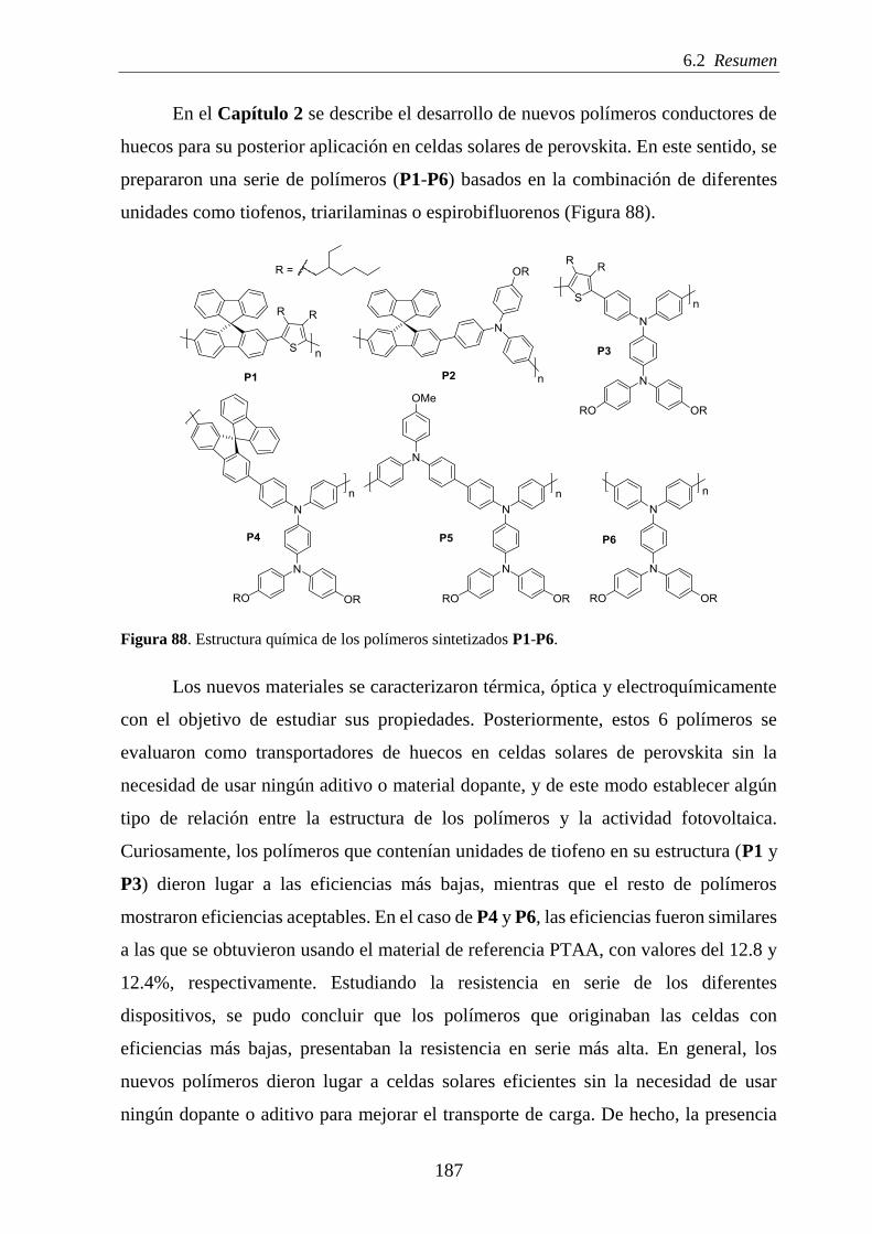
6.2 Resumen
187
En el Capítulo 2 se describe el desarrollo de nuevos polímeros conductores de
huecos para su posterior aplicación en celdas solares de perovskita. En este sentido, se
prepararon una serie de polímeros (P1-P6) basados en la combinación de diferentes
unidades como tiofenos, triarilaminas o espirobifluorenos (Figura 88).
Figura 88. Estructura química de los polímeros sintetizados P1-P6.
Los nuevos materiales se caracterizaron térmica, óptica y electroquímicamente
con el objetivo de estudiar sus propiedades. Posteriormente, estos 6 polímeros se
evaluaron como transportadores de huecos en celdas solares de perovskita sin la
necesidad de usar ningún aditivo o material dopante, y de este modo establecer algún
tipo de relación entre la estructura de los polímeros y la actividad fotovoltaica.
Curiosamente, los polímeros que contenían unidades de tiofeno en su estructura (P1 y
P3) dieron lugar a las eficiencias más bajas, mientras que el resto de polímeros
mostraron eficiencias aceptables. En el caso de P4 y P6, las eficiencias fueron similares
a las que se obtuvieron usando el material de referencia PTAA, con valores del 12.8 y
12.4%, respectivamente. Estudiando la resistencia en serie de los diferentes
dispositivos, se pudo concluir que los polímeros que originaban las celdas con
eficiencias más bajas, presentaban la resistencia en serie más alta. En general, los
nuevos polímeros dieron lugar a celdas solares eficientes sin la necesidad de usar
ningún dopante o aditivo para mejorar el transporte de carga. De hecho, la presencia

6 Summary/Resumen
188
de aditivos o dopantes se ha relacionado con la degradación de las celdas, por lo que la
posibilidad de trabajar sin aditivos o dopantes es sin duda un gran paso hacia la mejora
de la estabilidad de éste tipo de celdas. Además, se demostró que los dispositivos
fabricados usando los polímeros P4 y P6 tenían una mayor estabilidad térmica
comparada con los dispositivos que usaban el material de referencia PTAA.
En el Capítulo 3 se presenta una nueva estrategia para mejorar la calidad de la
capa de perovskita, lo que es de gran importancia para alcanzar tanto una buena
eficiencia como estabilidad en las celdas solares de perovskita. En este sentido, la
incorporación de aditivos a la capa de perovskita ha demostrado ser una estrategia
adecuada para mejorar la calidad de dicha capa. En este trabajo, se han desarrollado
tres nuevos semiconductores orgánicos (S1, P7 y P8) con cadenas perfluoradas en su
estructura para su uso como aditivos en celdas solares de perovskita. Cada material
contiene 26 átomos de flúor por unidad, lo que constituye la mayor cantidad de átomos
de flúor que se ha reportado para aditivos en este tipo de celdas (Figura 89).
Figura 89. Estructura química de los materiales S1, P7 y P8.
Se han sintetizado dos nuevos polímeros (P7 y P8) y una molécula (S1) y
estudiado sus propiedades químicas, térmicas y optoelectrónicas. Además, los nuevos
materiales se incorporaron a la capa de perovskita como aditivos y se estudió el efecto
que tenían en la formación de dicha capa, en la estabilidad y en el funcionamiento de
las celdas solares. En este contexto, las capas de perovskita que contenían aditivos

6.2 Resumen
189
mostraban cristales más grandes, lo que implica menos límites de granos, comparado
con las capas sin dopar. Además, se estudió la estabilidad de celdas solares, donde la
capa de perovskita se había tratado con los aditivos. Para este fin, se eligieron S1 y P7
para comprobar de qué manera la incorporación de moléculas y compuestos de
naturaleza polimérica, respectivamente, afectaba a la estabilidad de los dispositivos.
Como resultado, las celdas basadas en S1 y P7 mostraron una mayor estabilidad
comparada con la celda de referencia (sin aditivos), manteniendo el 94 y el 85% de su
potencia inicial, respectivamente, después de 80 minutos, mientras que los dispositivos
de referencia se destruían completamente, medidos bajo las mismas condiciones. Es
importante destacar que el carácter semiconductor de los nuevos aditivos podría estar
favoreciendo el transporte de carga, permitiendo de este modo, que el dispositivo
basado en S1 alcanzase un valor de eficiencia del 17%. Por tanto, los nuevos materiales
perfluorados garantizan tanto una buena eficiencia como estabilidad en celdas solares
de perovskita.
En el Capítulo 4 se ha diseñado y sintetizado una nueva familia de polímeros
(P9-P11) basados en bis(naftaleno diimidas), con el potencial de ser usados como
materiales trasportadores de electrones en celdas solares de perovskita. Además, se
sintetizaron una serie de moléculas basadas en la unidad de bis(naftaleno diimida)
(MC1-MC3) con fragmentos idénticos a los de los polímeros P9-P11, con el objetivo
de hacer una comparación entre moléculas y polímeros (Figura 90).
Los polímeros están compuestos de una unidad de benceno en combinación con
diferentes unidades de bis(naftaleno dimida), que son muy conocidas por poseer una
gran habilidad para transportar electrones, así como la capacidad para bloquear huecos.
Además, los polímeros fueron diseñados para ser procesados en disolución, para lo que
se introdujeron cadenas alquílicas en la unidad de benceno. Los materiales se
caracterizaron térmica, óptica y electroquímicamente para evaluar si eran aptos para
ser utilizados como transportadores de electrones en celdas solares de perovskita. A
este respecto, los polímeros presentaban unos niveles electrónicos adecuados y gran
estabilidad térmica, sin cambios de fases en el rango de temperatura en el que suelen
funcionar este tipo de celdas. En vista a las propiedades, los polímeros serían

6 Summary/Resumen
190
candidatos adecuados para utilizarlos como transportadores de electrones en celdas
solares de perovskita.
Figura 90. Estructuras químicas de los polímeros P9-P11 y de las moléculas MC1-MC3.
Además, se estudiaron las propiedades de transporte de cargas de las moléculas
MC1-MC3. Tanto MC2 como MC3, que tienen fragmentos con amina terciaria y
cuaternaria, respectivamente, mostraron mayor pseudo-fotoconductividad en
comparación con la molécula MC1. Los polímeros P9-P11 tienen los mismos
fragmentos estructurales que las moléculas MC1-MC3. Por lo tanto, en principio, se
podría esperar la misma tendencia en las propiedades de transporte de carga en estos
polímeros. Para confirmar esta hipótesis, actualmente se está colaborando con el Prof.
Seki de la Universidad de Kyoto (Japón). En cualquier caso, para demostrar la
aplicabilidad de los polímeros propuestos, se deben de probar como materiales
trasportadores de electrones en celdas solares de perovskita.

7. REFERENCES

7 References
193
7 REFERENCES
[1] https://www.worldenergy.org/work-programme/strategic-insight/survey-of-
energy-resources-and-technologies/.
[2] A. P. Mathews, Procedia Comput. Sci., 2014, 32, 731–737.
[3] https://scripps.ucsd.edu/programs/keelingcurve/.
[4] J. A. Church, N. J. White, Geophys. Res. Lett., 2006, 33, L01602.
[5] K. E. Kunkel, T. R. Karl, D. R. Easterling, K. Redmond, J. Young, X. Yin, P.
Hennon, Geophys. Res. Lett., 2013, 40, 1402–1408.
[6] K. E. Kunkel, T. R. Karl, H. Brooks, J. Kossin, J. H. Lawrimore, D. Arndt, L.
Bosart, D. Changnon, S. L. Cutter, N. Doesken, K. Emanuel, P. Y. Groisman, R.
W. Katz, T. Knutson, J. O’Brien, C. J. Paciorek, T. C. Peterson, K. Redmond, D.
Robinson, J. Trapp, R. Vose, S. Weaver, M. Wehner, K. Wolter, D. Wuebbles,
Am. Meteorol. Soc., 2013, 94, 499–514.
[7] https://climate.nasa.gov/images-of-change?id=623#623-arctic-sea-ice-
coverage-hits-record-low.
[8] Outlook for Energy: A View to 2040, 2018.
[9] International Energy Outlook, 2017.
[10] UNFCCC. 2015 Adoption of the Paris Agreement. I: Proposal by the President
(Draft Decision), United Nations Office, Geneva (Switzerland). 1–105.
[11] D. Reckien, M. Salvia, O. Heidrich, J. M. Church, F. Pietrapertosa, S. De
Gregorio-Hurtado, V. D’Alonzo, A. Foley, S. G. Simoes, E. K. Lorencová, H.
Orru, K. Orru, A. Wejs, J. Flacke, M. Olazabal, D. Geneletti, E. Feliu, S. Vasilie,
C. Nador, A. Krook-Riekkola, M. Matosović, P. A. Fokaides, B. I. Ioannou, A.
Flamos, N.-A. Spyridaki, M. V. Balzan, O. Fülöp, I. Paspaldzhiev, S. Grafakos,
R. Dawson, J. Clean. Prod., 2018, 191, 207–219.
[12] D. W. Cash, Energy Res. Soc. Sci., 2018, 35, 224–226.
[13] BP Statistical Review of World Energy, 2018.
[14] https://www.nytimes.com/2007/06/03/magazine/03wwln-essay-t.html.
[15] T. Wolfgang, Organic solar cells: Theory, Experiment, and Device Simulation;
Springer.; 2014.
[16] F. H. Alharbi, S. Kais, Renew. Sustain. Energy Rev., 2015, 43, 1073–1089.

7 References
194
[17] https://pveducation.org/.
[18] G. Antonicelli, Thesis, University of the Basque Country (Donostia-San
Sebastián), 2017.
[19] D. J. Friedman, Curr. Opin. Solid State Mater. Sci., 2010, 14, 131–138.
[20] S. Rühle, Sol. Energy, 2016, 130, 139–147.
[21] W. Shockley, H. J. Queisser, J. Appl. Phys., 1961, 32, 510–519.
[22] H. K. A. Shah, P. Torres, R. Tscharner, N. Wyrsch, Science, 1999, 285, 692–
699.
[23] A. E. Brooks, in Future Energy: Improved, Sustainable and Clean Options for
our Planet (Ed: Trevor Letcher); 2013; 383–404.
[24] C. Lin, in The Current Trends of Optics and Photonics (Ed: Chen-Chung Lee);
2015; 237–259.
[25] N. Marinova, S. Valero, J. L. Delgado, J. Colloid Interface Sci., 2017, 488, 373–
389.
[26] J. Jean, P. R. Brown, R. L. Jaffe, T. Buonassisi, V. Bulović, Energy Environ.
Sci., 2015, 8, 1200–1219.
[27] T. D. Lee, A. U. Ebong, Renew. Sustain. Energy Rev., 2017, 70, 1286–1297.
[28] A. Mohammad Bagher, M. Mahmoud Abadi Vahid, Am. J. Opt. Photonics, 2015,
3, 94–113.
[29] M. A. Green, Y. Hishikawa, E. D. Dunlop, D. H. Levi, M. A. Green, J. Hohl, E.
Masahiro, Y. Anita, W. Y. H. Baillie, Prog. Photovoltaics Res. Appl., 2019, 27,
3–12.
[30] T. Ibn-Mohammed, S. C. L. Koh, I. M. Reaney, A. Acquaye, G. Schileo, K. B.
Mustapha, R. Greenough, Renew. Sustain. Energy Rev., 2017, 80, 1321–1344.
[31] https://energyeducation.ca/encyclopedia/types_of_photovoltaic_cells.
[32] K. L. Chopra, P. D. Paulson, V. Dutta, Prog. Photovoltaics Res. Appl., 2004, 12,
69–92.
[33] W. Qarony, M. I. Hossain, M. K. Hossain, U. M. Jalal, A. Haque, A. R. Saad, Y.
H. Tsang, Results Phys., 2017, 7, 4287–4293.
[34] H. Sai, T. Matsui, T. Koida, K. Matsubara, M. Kondo, S. Sugiyama, H.
Katayama, Y. Takeuchi, I. Yoshida, Appl. Phys. Lett., 2015, 106, 213902.
[35] G. H. Carey, A. L. Abdelhady, Z. Ning, S. M. Thon, O. M. Bakr, E. H. Sargent,

7 References
195
Chem. Rev., 2015, 115, 12732–12763.
[36] NREL Chart of Best Research-Cell Efficiencies (https://www.nrel.gov/pv/cell-
efficiency.html), 2019.
[37] N. Kaur, M. Singh, D. Pathak, T. Wagner, J. M. Nunzi, Synth. Met., 2014, 190,
20–26.
[38] G. J. Hedley, A. Ruseckas, I. D. W. Samuel, Chem. Rev., 2017, 117, 796–837.
[39] M. Privado, C. R. Seco, R. Singhal, P. D. La Cruz, F. Langa, G. D. Sharma, E.
Palomares, ACS Energy Lett., 2018, 3, 2418–2424.
[40] G. N. Tiwari, R. K. Mishra, S. C. Solanki, Appl. Energy, 2011, 88, 2287–2304.
[41] H. Youn, H. J. Park, L. J. Guo, Small, 2015, 11, 2228–2246.
[42] V. Cuesta, R. Singhal, P. De La Cruz, G. D. Sharma, F. Langa, ACS Appl. Mater.
Interfaces, 2019, 11, 7216–7225.
[43] P. Hudhomme, EPJ Photovoltaics, 2013, 4, 40401.
[44] B. O’Regan, M. Gratzel, Nature, 1991, 353, 737–740.
[45] A. Hagfeldt, Ambio, 2012, 41, 151–155.
[46] M. Pazoki, U. B. Cappel, E. M. J. Johansson, A. Hagfeldt, G. Boschloo, Energy
Environ. Sci., 2017, 10, 672–709.
[47] S. Shi, Y. Li, X. Li, H. Wang, Mater. Horizons, 2015, 2, 378–405.
[48] S. Mathew, A. Yella, P. Gao, R. Humphry-Baker, B. F. E. Curchod, N. Ashari-
Astani, I. Tavernelli, U. Rothlisberger, M. K. Nazeeruddin, M. Grätzel, Nat.
Chem., 2014, 6, 242–247.
[49] U. Bach, D. Lupo, P. Comte, J. E. Moser, F. Weissörtel, J. Salbeck, H. Spreitzer,
M. Grätzel, Nature, 1998, 395, 583–585.
[50] A. Andualem, S. Demiss, Edelweiss Appli Sci Tech., 2018, 2, 145–150.
[51] A. Kojima, K. Teshima, Y. Shirai, T. Miyasaka, J. Am. Chem. Soc., 2009, 131,
6050–6051.
[52] J. Im, C. Lee, J. Lee, S. Park, N. Park, Nanoscale, 2011, 3, 4088–4093.
[53] H. Kim, C. Lee, J. Im, K. Lee, T. Moehl, A. Marchioro, S. Moon, R. Humphry-
baker, J. Yum, J. E. Moser, M. Gra, N.-G. Park, Sci. Rep., 2012, 2, 591.
[54] T. M. Brenner, D. A. Egger, L. Kronik, G. Hodes, D. Cahen, Nat. Rev. Mater.,
2016, 1, 15007.

7 References
196
[55] N. Park, Mater. Today, 2015, 18, 65–72.
[56] X. Tong, Z. M. Wang, J. Electron. Sci. Technol., 2017, 15, 326–332.
[57] A. R. B. M. Yusoff, M. K. Nazeeruddin, J. Phys. Chem. Lett., 2016, 7, 851–866.
[58] Y. Zhao, K. Zhu, Chem. Soc. Rev., 2016, 45, 655–689.
[59] Q. Lin, A. Armin, P. L. Burn, P. Meredith, Acc. Chem. Res., 2016, 49, 545–553.
[60] S. Gholipour, M. Saliba, Small, 2018, 14, 1802385.
[61] C. R. Kalaiselvi, N. Muthukumarasamy, D. Velauthapillai, M. Kang, T. S.
Senthil, Mater. Lett., 2018, 219, 198–200.
[62] A. K. Jena, A. Kulkarni, T. Miyasaka, Chem. Rev., 2019, 119, 3036–3103.
[63] S. De Wolf, J. Holovsky, S. J. Moon, P. Löper, B. Niesen, M. Ledinsky, F. J.
Haug, J. H. Yum, C. Ballif, J. Phys. Chem. Lett., 2014, 5, 1035–1039.
[64] M. A. Green, A. Ho-Baillie, ACS Energy Lett., 2017, 2, 822–830.
[65] H. S. Jung, N. G. Park, Small, 2015, 11, 10–25.
[66] W. J. Yin, T. Shi, Y. Yan, Adv. Mater., 2014, 26, 4653–4658.
[67] B. Wang, X. Xiao, T. Chen, Nanoscale, 2014, 6, 12287–12297.
[68] G. Xing, N. Mathews, S. Sun, S. S. Lim, Y. M. Lam, M. Graẗzel, S. Mhaisalkar,
T. C. Sum, Science, 2013, 342, 344–347.
[69] C. Motta, F. El-Mellouhi, S. Sanvito, Sci. Rep., 2015, 5, 12746.
[70] T. C. Sum, N. Mathews, Energy Environ. Sci., 2014, 7, 2518–2534.
[71] A. Jha, H. G. Duan, V. Tiwari, P. K. Nayak, H. J. Snaith, M. Thorwart, R. J.
Dwayne Miller, ACS Photonics, 2018, 5, 852–860.
[72] W. Wang, Y. Li, X. Wang, Y. Lv, S. Wang, K. Wang, Y. Shi, L. Xiao, Z. Chen,
Q. Gong, Phys. Rev. B, 2016, 94, 140302.
[73] V. D’Innocenzo, G. Grancini, M. J. P. Alcocer, A. R. S. Kandada, S. D. Stranks,
M. M. Lee, G. Lanzani, H. J. Snaith, A. Petrozza, Nat. Commun., 2014, 5, 3586.
[74] C. Sheng, C. Zhang, Y. Zhai, K. Mielczarek, W. Wang, W. Ma, A. Zakhidov, Z.
V. Vardeny, Phys. Rev. Lett., 2015, 114, 116601.
[75] Z. Zhao, W. Sun, Y. Li, S. Ye, H. Rao, F. Gu, Z. Liu, Z. Bian, C. Huang, J.
Mater. Chem. A, 2017, 5, 4756–4773.
[76] T. Salim, S. Sun, Y. Abe, A. Krishna, A. C. Grimsdale, Y. M. Lam, J. Mater.

7 References
197
Chem. A, 2015, 3, 8943–8969.
[77] S. F. Völker, S. Collavini, J. L. Delgado, ChemSusChem, 2015, 8, 3012–3028.
[78] B. J. Kim, S. Lee, H. S. Jung, J. Mater. Chem. A, 2018, 6, 12215–12236.
[79] C. H. Ng, H. N. Lim, S. Hayase, Z. Zainal, N. M. Huang, Renew. Sustain. Energy
Rev., 2018, 90, 248–274.
[80] F. Li, M. Liu, J. Mater. Chem. A, 2017, 5, 15447–15459.
[81] I. Hwang, I. Jeong, J. Lee, M. J. Ko, K. Yong, ACS Appl. Mater. Interfaces, 2015,
7, 17330–17336.
[82] J. You, L. Meng, T. Bin Song, T. F. Guo, W. H. Chang, Z. Hong, H. Chen, H.
Zhou, Q. Chen, Y. Liu, N. De Marco, Y. Yang, Nat. Nanotechnol., 2016, 11, 75–
81.
[83] J. Yang, B. D. Siempelkamp, D. Liu, T. L. Kelly, ACS Nano, 2015, 9, 1955–
1963.
[84] A. M. A. Leguy, Y. Hu, M. Campoy-Quiles, M. I. Alonso, O. J. Weber, P.
Azarhoosh, M. Van Schilfgaarde, M. T. Weller, T. Bein, J. Nelson, P. Docampo,
P. R. F. Barnes, Chem. Mater., 2015, 27, 3397–3407.
[85] D. Wang, M. Wright, N. K. Elumalai, A. Uddin, Sol. Energy Mater. Sol. Cells,
2016, 147, 255–275.
[86] G. W. Kim, G. Kang, M. Malekshahi Byranvand, G. Y. Lee, T. Park, ACS Appl.
Mater. Interfaces, 2017, 9, 27720–27726.
[87] Q. Fu, X. Tang, B. Huang, T. Hu, L. Tan, L. Chen, Y. Chen, Adv. Sci., 2018, 5,
1700387.
[88] T. Leijtens, G. E. Eperon, S. Pathak, A. Abate, M. M. Lee, H. J. Snaith, Nat.
Commun., 2013, 4, 2885.
[89] S. Ito, S. Tanaka, K. Manabe, H. Nishino, J. Phys. Chem. C, 2014, 118, 16995–
17000.
[90] D. Liu, Y. Liu, J. Semicond., 2017, 38, 011005.
[91] I. Mesquita, L. Andrade, A. Mendes, Renew. Sustain. Energy Rev., 2018, 82,
2471–2489.
[92] B. Salhi, Y. S. Wudil, M. K. Hossain, A. Al-Ahmed, F. A. Al-Sulaiman, Renew.
Sustain. Energy Rev., 2018, 90, 210–222.
[93] E. Raza, F. Aziz, Z. Ahmad, RSC Adv., 2018, 8, 20952–20967.

7 References
198
[94] B. Philippe, B. W. Park, R. Lindblad, J. Oscarsson, S. Ahmadi, E. M. J.
Johansson, H. Rensmo, Chem. Mater., 2015, 27, 1720–1731.
[95] P. S. Whitfield, N. Herron, W. E. Guise, K. Page, Y. Q. Cheng, I. Milas, M. K.
Crawford, Sci. Rep., 2016, 6, 35685.
[96] M. R. Leyden, Y. Jiang, Y. Qi, J. Mater. Chem. A, 2016, 4, 13125–13132.
[97] L. Cojocaru, S. Uchida, Y. Sanehira, V. Gonzalez-Pedro, J. Bisquert, J.
Nakazaki, T. Kubo, H. Segawa, Chem. Lett., 2015, 44, 1557–1559.
[98] M. Yavari, M. Mazloum-Ardakani, S. Gholipour, N. Marinova, J. L. Delgado, S.
H. Turren-Cruz, K. Domanski, N. Taghavinia, M. Saliba, M. Grätzel, A.
Hagfeldt, W. Tress, Adv. Energy Mater., 2018, 8, 1702719.
[99] Z. Shi, J. Guo, Y. Chen, Q. Li, Y. Pan, H. Zhang, Y. Xia, W. Huang, Adv. Mater.,
2017, 29, 1605005.
[100] A. Abate, Joule, 2017, 1, 659–664.
[101] M. Lyu, J. H. Yun, P. Chen, M. Hao, L. Wang, Adv. Energy Mater., 2017, 7,
1602512.
[102] I. Kopacic, B. Friesenbichler, S. F. Hoefler, B. Kunert, H. Plank, T. Rath, G.
Trimmel, ACS Appl. Energy Mater., 2018, 1, 343–347.
[103] F. Hao, C. C. Stoumpos, D. H. Cao, R. P. H. Chang, M. G. Kanatzidis, Nat.
Photonics, 2014, 8, 489–494.
[104] N. Ito, M. A. Kamarudin, D. Hirotani, Y. Zhang, Q. Shen, Y. Ogomi, S. Iikubo,
T. Minemoto, K. Yoshino, S. Hayase, J. Phys. Chem. Lett., 2018, 9, 1682–1688.
[105] N. Kumari, S. R. Patel, J. V Gohel, J. Mater. Sci. Mater. Electron., 2018, 29,
18144–18150.
[106] P. Liu, W. Wang, S. Liu, H. Yang, Z. Shao, Adv. Energy Mater., 2019, 9,
1803017.
[107] N. K. Elumalai, A. Uddin, Sol. Energy Mater. Sol. Cells, 2016, 157, 476–509.
[108] M. Yang, Y. Zhou, Y. Zeng, C. S. Jiang, N. P. Padture, K. Zhu, Adv. Mater.,
2015, 27, 6363–6370.
[109] L. Cai, L. Liang, J. Wu, B. Ding, L. Gao, B. Fan, J. Semicond., 2017, 38, 014006.
[110] Y. Hu, S. Si, A. Mei, Y. Rong, H. Liu, X. Li, H. Han, Sol. RRL, 2017, 1, 1600019.
[111] L. Calió, S. Kazim, M. Grätzel, S. Ahmad, Angew. Chem. Int. Ed., 2016, 55,
14522–14545.

7 References
199
[112] X. Yang, H. Wang, B. Cai, Z. Yu, L. Sun, J. Energy Chem., 2018, 27, 650–672.
[113] Z. Yu, L. Sun, Small Methods, 2018, 2, 1700280.
[114] Z. H. Bakr, Q. Wali, A. Fakharuddin, L. Schmidt-Mende, T. M. Brown, R. Jose,
Nano Energy, 2017, 34, 271–305.
[115] Y. Shao, Y. Yuan, J. Huang, Nat. Energy, 2016, 1, 15001.
[116] J. Urieta-Mora, I. García-Benito, A. Molina-Ontoria, N. Martín, Chem. Soc. Rev.,
2018, 47, 8541–8571.
[117] Z. Yu, L. Sun, Adv. Energy Mater., 2015, 5, 1500213.
[118] X. Zhao, M. Wang, Mater. Today Energy, 2018, 7, 208–220.
[119] P. Vivo, J. K. Salunke, A. Priimagi, Materials, 2017, 10, 1087.
[120] R. Misra, G. SivaKumar, J. Mater. Chem. A, 2018, 6, 18750–18765.
[121] J. Salbeck, J. Bauer, F. Weissgrtel, H. Bestgen, Synth. Met., 1997, 91, 209–215.
[122] Z. Hawash, L. K. Ono, Y. Qi, Adv. Mater. Interfaces, 2018, 5, 1700623.
[123] N. J. Jeon, J. Lee, J. H. Noh, M. K. Nazeeruddin, S. Il Seok, J. Am. Chem. Soc.,
2013, 135, 19087–19090.
[124] B. Xu, J. Zhang, Y. Hua, P. Liu, L. Wang, C. Ruan, Y. Li, G. Boschloo, E. M. J.
Johansson, L. Kloo, A. Hagfeldt, A. K. Y. Jen, L. Sun, Chem, 2017, 2, 676–687.
[125] T. Malinauskas, D. Tomkute-Luksiene, R. Sens, M. Daskeviciene, R. Send, H.
Wonneberger, V. Jankauskas, I. Bruder, V. Getautis, ACS Appl. Mater.
Interfaces., 2015, 7, 11107–11116.
[126] G. Divitini, S. Cacovich, F. Matteocci, L. Cinà, A. Di Carlo, C. Ducati, Nat.
Energy, 2016, 1, 15012.
[127] J. Burschka, Thesis, École polytechnique fédérale de Lausanne (Laussane),
2013.
[128] G. Niu, X. Guo, L. Wang, J. Mater. Chem. A, 2015, 3, 8970–8980.
[129] C. D. Bailie, E. L. Unger, S. M. Zakeeruddin, M. Grätzel, M. D. McGehee, Phys.
Chem. Chem. Phys., 2014, 16, 4864–4870.
[130] A. Krishna, A. C. Grimsdale, J. Mater. Chem. A, 2017, 5, 16446–16466.
[131] M. Ulfa, T. Zhu, F. Goubard, T. Pauporté, J. Mater. Chem. A, 2018, 6, 13350–
13358.
[132] B. Roose, Q. Wang, A. Abate, Adv. Energy Mater., 2018, 9, 1803140.

7 References
200
[133] W. S. Yang, B.-W. Park, E. H. Jung, N. J. Jeon, Y. C. Kim, D. U. Lee, S. S. Shin,
J. Seo, E. K. Kim, J. H. Noh, S. Il Seok, Science, 2017, 356, 1376–1379.
[134] P. Qin, N. Tetreault, M. I. Dar, P. Gao, K. L. McCall, S. R. Rutter, S. D. Ogier,
N. D. Forrest, J. S. Bissett, M. J. Simms, A. J. Page, R. Fisher, M. Grätzel, M.
K. Nazeeruddin, Adv. Energy Mater., 2015, 5, 1400980.
[135] K. Sun, S. Zhang, P. Li, Y. Xia, X. Zhang, D. Du, F. H. Isikgor, J. Ouyang, J.
Mater. Sci. Mater. Electron., 2015, 26, 4438–4462.
[136] J. H. Heo, H. J. Han, D. Kim, T. K. Ahn, S. H. Im, Energy Environ. Sci., 2015,
8, 1602–1608.
[137] H. A. Abbas, R. Kottokkaran, B. Ganapathy, M. Samiee, L. Zhang, A. Kitahara,
M. Noack, V. L. Dalal, APL Mater., 2015, 3, 016105.
[138] J. Xiao, J. Shi, H. Liu, Y. Xu, S. Lv, Y. Luo, D. Li, Q. Meng, Y. Li, Adv. Energy
Mater., 2015, 5, 1401943.
[139] S. N. Habisreutinger, T. Leijtens, G. E. Eperon, S. D. Stranks, R. J. Nicholas, H.
J. Snaith, Nano Lett., 2014, 14, 5561–5568.
[140] P. Zhou, T. Bu, S. Shi, L. Li, Y. Zhang, Z. Ku, Y. Peng, J. Zhong, Y. B. Cheng,
F. Huang, J. Mater. Chem. C, 2018, 6, 5733–5737.
[141] M. Wong-Stringer, J. E. Bishop, J. A. Smith, D. K. Mohamad, A. J. Parnell, V.
Kumar, C. Rodenburg, D. G. Lidzey, J. Mater. Chem. A, 2017, 5, 15714–15723.
[142] Z. Yu, Y. Zhang, X. Jiang, X. Li, J. Lai, M. Hu, M. Elawad, G. G. Gurzadyan,
X. Yang, L. Sun, RSC Adv., 2017, 7, 27189–27197.
[143] B. Cai, Y. Xing, Z. Yang, W. H. Zhang, J. Qiu, Energy Environ. Sci., 2013, 6,
1480–1485.
[144] Y. S. Kwon, J. Lim, H. J. Yun, Y. H. Kim, T. Park, Energy Environ. Sci., 2014,
7, 1454–1460.
[145] J. M. Marin-Beloqui, J. Pérez Hernández, E. Palomares, Chem. Commun., 2014,
50, 14566–14569.
[146] Z. Zhu, Y. Bai, H. Ka, H. Lee, C. Mu, T. Zhang, L. Zhang, Adv. Funct. Mater.,
2014, 24, 7357–7365.
[147] G.-W. Kim, G. Kang, J. Kim, G.-Y. Lee, H. Il Kim, L. Pyeon, J. Lee, T. Park,
Energy Environ. Sci., 2016, 9, 2326–2333.
[148] C. Huang, W. Fu, C.-Z. Li, Z. Zhang, W. Qiu, M. Shi, P. Heremans, A. K.-Y.
Jen, H. Chen, J. Am. Chem. Soc., 2016, 138, 2528–2531.
[149] S. Paek, P. Qin, Y. Lee, K. T. Cho, P. Gao, G. Grancini, E. Oveisi, P. Gratia, K.

7 References
201
Rakstys, S. A. Al-Muhtaseb, C. Ludwig, J. Ko, M. K. Nazeeruddin, Adv. Mater.,
2017, 29, 1606555.
[150] F. Zhang, X. Zhao, C. Yi, D. Bi, X. Bi, P. Wei, X. Liu, S. Wang, X. Li, S. M.
Zakeeruddin, M. Grätzel, Dyes Pigm., 2017, 136, 273–277.
[151] K. Rakstys, S. Paek, P. Gao, P. Gratia, T. Marszalek, G. Grancini, K. T. Cho, K.
Genevicius, V. Jankauskas, W. Pisula, M. K. Nazeeruddin, J. Mater. Chem. A,
2017, 5, 7811–7815.
[152] M. Sun, X. Liu, F. Zhang, H. Liu, X. Liu, S. Wang, Y. Xiao, D. Li, Q. Meng, X.
Li, Appl. Surf. Sci., 2017, 416, 124–132.
[153] X. Liu, F. Zhang, Z. Liu, Y. Xiao, S. Wang, X. Li, J. Mater. Chem. C, 2017, 5,
11429–11435.
[154] S. F. Völker, M. Vallés-Pelarda, J. Pascual, S. Collavini, F. Ruipérez, E. Zuccatti,
L. E. Hueso, R. Tena-Zaera, I. Mora-Seró, J. L. Delgado, Chem. A Eur. J., 2018,
24, 8524–8529.
[155] H. D. Pham, T. T. Do, J. Kim, C. Charbonneau, S. Manzhos, K. Feron, W. C.
Tsoi, J. R. Durrant, S. M. Jain, P. Sonar, Adv. Energy Mater., 2018, 8, 1703007.
[156] G. W. Kim, J. Lee, G. Kang, T. Kim, T. Park, Adv. Energy Mater., 2017,
1701935.
[157] T. Matsui, I. Petrikyte, T. Malinauskas, K. Domanski, M. Daskeviciene, M.
Steponaitis, P. Gratia, W. Tress, J. P. Correa-Baena, A. Abate, A. Hagfeldt, M.
Grätzel, M. K. Nazeeruddin, V. Getautis, M. Saliba, ChemSusChem, 2016, 9,
2567–2571.
[158] A. Dubey, N. Adhikari, S. Venkatesan, S. Gu, D. Khatiwada, Q. Wang, L.
Mohammad, M. Kumar, Q. Qiao, Sol. Energy Mater. Sol. Cells, 2016, 145, 193–
199.
[159] X. Jiang, Z. Yu, Y. Zhang, J. Lai, J. Li, G. G. Gurzadyan, X. Yang, L. Sun, Sci.
Rep., 2017, 7, 42564.
[160] P. Agarwala, D. Kabra, J. Mater. Chem. A, 2017, 5, 1348–1373.
[161] I. R. Perera, A. Gupta, W. Xiang, T. Daeneke, U. Bach, R. A. Evans, C. A. Ohlin,
L. Spiccia, Phys. Chem. Chem. Phys., 2014, 16, 12021–12028.
[162] S. M. Park, K. S. Yook, W. H. Lee, Y. Hong, J. Y. Lee, I. N. Kang, J. Polym.
Sci. Part A. Polym. Chem., 2013, 51, 5111–5117.
[163] K. Neumann, C. Schwarz, A. Köhler, M. Thelakkat, J. Phys. Chem. C, 2014,
118, 27–36.
[164] X. Zhang, S. Cao, L. Huang, L. Chen, X. Ouyang, Dyes Pigm., 2017, 145, 110–

7 References
202
115.
[165] M. R. Talipov, M. M. Hossain, A. Boddeda, K. Thakur, R. Rathore, Org. Biomol.
Chem., 2016, 14, 2961–2968.
[166] S. F. Völker, T. Dellermann, H. Ceymann, M. Holzapfel, C. Lambert, J. Polym.
Sci. Part A. Polym. Chem., 2014, 52, 890–911.
[167] T. Leijtens, I. K. Ding, T. Giovenzana, J. T. Bloking, M. D. McGehee, A.
Sellinger, ACS Nano, 2012, 6, 1455–1462.
[168] M. Deepa, M. Salado, L. Calio, S. Kazim, S. M. Shivaprasad, S. Ahmad, Phys.
Chem. Chem. Phys., 2017, 19, 4069–4077.
[169] A. K. Baranwal, S. Kanaya, T. A. N. Peiris, G. Mizuta, T. Nishina, H. Kanda, T.
Miyasaka, H. Segawa, S. Ito, ChemSusChem, 2016, 9, 2604–2608.
[170] T. Leijtens, G. E. Eperon, N. K. Noel, S. N. Habisreutinger, A. Petrozza, H. J.
Snaith, Adv. Energy Mater., 2015, 5, 1500963.
[171] K. Poorkazem, T. L. Kelly, Sustain. Energy Fuels, 2018, 2, 1332–1341.
[172] N. J. Jeon, J. H. Noh, W. S. Yang, Y. C. Kim, S. Ryu, J. Seo, S. Il Seok, Nature,
2014, 517, 476–480.
[173] M. Saliba, T. Matsui, J. Y. Seo, K. Domanski, J. P. Correa-Baena, M. K.
Nazeeruddin, S. M. Zakeeruddin, W. Tress, A. Abate, A. Hagfeldt, M. Grätzel,
Energy Environ. Sci., 2016, 9, 1989–1997.
[174] F. Bella, G. Griffini, J. P. Correa-Baena, G. Saracco, M. Grätzel, A. Hagfeldt, S.
Turri, C. Gerbaldi, Science, 2016, 354, 203–206.
[175] Z. Yang, A. Rajagopal, C. Chueh, S. B. Jo, B. Liu, T. Zhao, A. K. Jen, Adv.
Mater., 2016, 28, 8990–8997.
[176] S. Paek, P. Schouwink, E. N. Athanasopoulou, K. T. Cho, G. Grancini, Y. Lee,
Y. Zhang, F. Stellacci, M. K. Nazeeruddin, P. Gao, Chem. Mater., 2017, 29,
3490–3498.
[177] F. Huang, Y. Dkhissi, W. Huang, M. Xiao, I. Benesperi, S. Rubanov, Y. Zhu, X.
Lin, L. Jiang, Y. Zhou, A. Gray-weale, J. Etheridge, C. R. Mcneill, R. A. Caruso,
U. Bach, L. Spiccia, Y. Cheng, Nano Energy, 2014, 10, 10–18.
[178] N. J. Jeon, J. H. Noh, Y. C. Kim, W. S. Yang, S. Ryu, S. Il Seok, Nat. Mater.,
2014, 13, 897–903.
[179] M. Xiao, L. Zhao, M. Geng, Y. Li, B. Dong, Z. Xu, L. Wan, W. Li, S. Wang,
Nanoscale, 2018, 10, 12141–12148.
[180] T. Li, Y. Pan, Z. Wang, Y. Xia, Y. Chen, W. Huang, J. Mater. Chem. A, 2017,

7 References
203
5, 12602–12652.
[181] D. Bi, X. Li, J. V Milic, D. J. Kubicki, N. Pellet, J. Luo, T. Lagrange, P. Mettraux,
L. Emsley, S. M. Zakeeruddin, M. Grätzel, Nat. Commun., 2018, 9, 4482.
[182] C. Zhang, M. Li, Z. Wang, Y. Jiang, H. Liu, Y. Yang, X. Gao, H. Ma, J. Mater.
Chem. A, 2017, 5, 2572–2579.
[183] B. Yang, O. Dyck, J. Poplawsky, J. Keum, A. Puretzky, S. Das, I. Ivanov, C.
Rouleau, G. Duscher, D. Geohegan, K. Xiao, J. Am. Chem. Soc., 2015, 137,
9210–9213.
[184] Y. Zhao, J. Wei, H. Li, Y. Yan, W. Zhou, D. Yu, Q. Zhao, Nat. Commun., 2016,
7, 10228.
[185] Y. Guo, K. Shoyama, W. Sato, E. Nakamura, Adv. Energy Mater., 2016, 6,
1502317.
[186] C. Zuo, L. Ding, Nanoscale, 2014, 6, 9935–9938.
[187] Y. Jeon, S. Lee, R. Kang, J. Kim, J. Yeo, S. Lee, S. Kim, J. Yun, D. Kim, Sci.
Rep., 2014, 4, 6953.
[188] P. Liang, C. Liao, C. Chueh, F. Zuo, S. T. Williams, X. Xin, J. Lin, A. K. Jen,
Adv. Mater., 2014, 26, 3748–3754.
[189] C. Gao, H. Dong, X. Bao, Y. Zhang, A. Saparbaev, L. Yu, S. Wen, R. Yang, L.
Dong, J. Mater. Chem. C, 2018, 6, 8234–8241.
[190] M. Sun, F. Zhang, H. Liu, X. Li, Y. Xiao, S. Wang, J. Mater. Chem. A, 2017, 5,
13448–13456.
[191] S. Collavini, M. Saliba, W. R. Tress, P. J. Holzhey, S. F. Völker, K. Domanski,
S. H. Turren-Cruz, A. Ummadisingu, S. M. Zakeeruddin, A. Hagfeldt, M.
Grätzel, J. L. Delgado, ChemSusChem, 2018, 11, 1032–1039.
[192] C. Chang, C. Chu, Y. Huang, C. Huang, S. Chang, C. Chen, C. Chao, W. Su,
ACS Appl. Mater. Interfaces, 2015, 7, 4955–4961.
[193] Q. Xue, Z. Hu, C. Sun, Z. Chen, F. Huang, H. Yip, Y. Cao, RSC Adv., 2015, 5,
775–783.
[194] Q. Dong, Z. Wang, K. Zhang, H. Yu, P. Huang, X. Liu, Y. Zhou, N. Chen, B.
Song, Nanoscale, 2016, 8, 5552–5558.
[195] B. Li, Y. Zhang, L. Fu, T. Yu, S. Zhou, L. Zhang, L. Yin, Nat. Commun., 2018,
9, 1076.
[196] F. Li, J. Yuan, X. Ling, Y. Zhang, Y. Yang, S. H. Cheung, Adv. Funct. Mater.,
2018, 28, 1706377.

7 References
204
[197] J. C. Yu, S. Badgujar, E. D. Jung, V. K. Singh, D. W. Kim, J. Gierschner, E. Lee,
Y. S. Kim, S. Cho, M. S. Kwon, M. H. Song, Adv. Mater., 2019, 31, 1805554.
[198] J. Jiang, Q. Wang, Z. Jin, X. Zhang, J. Lei, H. Bin, Z. Zhang, Adv. Energy Mater.,
2018, 8, 1701757.
[199] J. Pascual, I. Kosta, T. T. Ngo, A. Chuvilin, G. Cabanero, H. J. Grande, E. M.
Barea, I. Mora-Seró, J. L. Delgado, R. Tena-Zaera, ChemSusChem, 2016, 9,
2679–2685.
[200] R. Sandoval-Torrientes, J. Pascual, I. García-Benito, S. Collavini, I. Kosta, R.
Tena-Zaera, N. Martín, J. L. Delgado, ChemSusChem, 2017, 10, 2023–2029.
[201] Y. Takeda, T. L. Andrew, J. M. Lobez, A. J. Mork, T. M. Swager, Angew.
Commun., 2012, 51, 9042–9046.
[202] D. Wei, F. Ma, R. Wang, S. Dou, P. Cui, H. Huang, J. Ji, E. Jia, X. Jia, S. Sajid,
A. M. Elseman, L. Chu, Y. Li, B. Jiang, J. Qiao, Y. Yuan, M. Li, M. Li, Adv.
Mater., 2018, 30, 1707583.
[203] D. Bi, P. Gao, R. Scopelliti, E. Oveisi, J. Luo, M. Grätzel, A. Hagfeldt, K.
Nazeeruddin, Adv. Mater., 2016, 28, 2910–2915.
[204] M. Salado, F. J. Ramos, V. M. Manzanares, P. Gao, K. Nazeeruddin, P. J. Dyson,
S. Ahmad, ChemSusChem, 2016, 9, 2708–2714.
[205] M. Salado, M. Asunci, J. P. Holgado, S. Kazim, M. K. Nazeeruddin, P. J. Dyson,
S. Ahmad, ChemSusChem, 2017, 10, 3846–3853.
[206] K. M. M. Salim, T. M. Koh, D. Bahulayan, P. C. Harikesh, N. F. Jamaludin, B.
Febriansyah, A. Bruno, S. Mhaisalkar, N. Mathews, ACS Energy Lett., 2018, 3,
1068–1076.
[207] J. Yang, C. Liu, C. Cai, X. Hu, Z. Huang, X. Duan, X. Meng, Z. Yuan, L. Tan,
Y. Chen, Adv. Energy Mater., 2019, 9, 1900198.
[208] J. Lim, T. M. Swager, Angew. Chem. Int. Ed., 2010, 49, 7486–7488.
[209] T. Li, C. Su, S. B. Akula, W. Sun, H. Chien, W. Li, Org. Lett., 2016, 18, 3386–
3389.
[210] A. Facchetti, M. Yoon, C. L. Stern, G. R. Hutchison, M. A. Ratner, T. J. Marks,
J. Am. Chem. Soc., 2004, 126, 13480–13501.
[211] A. B. López, J. C. de la Cal, J. M. Asua, Langmuir, 2016, 32, 7459–7466.
[212] H. J. Son, W. Wang, T. Xu, Y. Liang, Y. Wu, G. Li, L. Yu, J. Am. Chem. Soc.,
2011, 133, 1885–1894.
[213] P. Calado, A. M. Telford, D. Bryant, X. Li, J. Nelson, B. C. O´Regan, P. R. F.

7 References
205
Barnes, Nat. Commun., 2016, 7, 13831.
[214] A. Dualeh, N. Tétreault, T. Moehl, P. Gao, Adv. Funct. Mater., 2014, 24, 3250–
3258.
[215] H. Yang, J. Zhang, C. Z, J. Chang, Z. Lin, D. Chen, H. Xi, Y. Hao, Materials,
2017, 10, 837.
[216] S. Masi, A. Rizzo, R. Munir, A. Listorti, A. Giuri, C. E. Corcione, N. D. Treat,
G. Gigli, A. Amassian, N. Stingelin, S. Colella, Adv. Funct. Mater, 2017, 7,
1602600.
[217] D. Bryant, N. Aristidou, S. Pont, I. Sanchez-molina, T. Chotchunangatchaval, S.
Wheeler, R. Durrant, S. A. Haque, Energy Environ. Sci., 2016, 9, 1655–1660.
[218] N. Marinova, F. M., I. Matulaitiene, A. Devizis, G. Niaura, V. Gulbinas, J. L.
Delgado, ChemSusChem, 2017, 10, 3760–3764.
[219] R. Schlaf, H. Murata, Z. H. Kafafi, J. Electron Spectrosc., 2001, 120, 149–154.
[220] E. J. Juarez-Perez, Z. Hawash, S. R. Raga, L. K. Ono, Y. Qi, Energy Environ.
Sci., 2016, 9, 3406–3410.
[221] F. Babudri, G. M. Farinola, F. Naso, R. Ragni, Chem. Commun., 2007, 1003–
1022.
[222] A. Marchioro, J. Teuscher, D. Friedrich, M. Kunst, R. Van De Krol, T. Moehl,
M. Grätzel, J. E. Moser, Nat. Photonics, 2014, 8, 250–255.
[223] G. Yang, H. Tao, P. Qin, W. Ke, G. Fang, J. Mater. Chem. A, 2016, 4, 3970–
3990.
[224] A. Isakova, P. D. Topham, J. Polym. Sci. Part B Polym. Phys., 2017, 55, 549–
568.
[225] W. Ke, G. Fang, J. Wan, H. Tao, Q. Liu, L. Xiong, P. Qin, J. Wang, H. Lei, G.
Yang, M. Qin, X. Zhao, Y. Yan, Nat. Commun., 2015, 6, 6700.
[226] S. Gharibzadeh, F. Valduga de Almeida Camargo, C. Roldán-Carmona, G. C.
Gschwend, J. Pascual, R. Tena-Zaera, G. Cerullo, G. Grancini, M. K.
Nazeeruddin, Adv. Mater., 2018, 30, 1801496.
[227] H. D. Pham, L. Xianqiang, W. Li, S. Manzhos, A. K. K. Kyaw, P. Sonar, Energy
Environ. Sci., 2019, 12, 1177–1209.
[228] S. K. Jung, D. S. Lee, M. H. Ann, S. H. Im, J. H. Kim, O. P. Kwon,
ChemSusChem, 2018, 11, 3835.
[229] J. Lian, B. Lu, F. Niu, P. Zeng, X. Zhan, Small Methods, 2018, 2, 1800082.

7 References
206
[230] H. Liu, Z. Huang, S. Wei, L. Zheng, L. Xiao, Q. Gong, Nanoscale, 2016, 8,
6209–6221.
[231] M. F. Mohamad Noh, C. H. Teh, R. Daik, E. L. Lim, C. C. Yap, M. A. Ibrahim,
N. Ahmad Ludin, A. R. Bin Mohd Yusoff, J. Jang, M. A. Mat Teridi, J. Mater.
Chem. C, 2018, 6, 682–712.
[232] S. Sun, T. Buonassisi, J. P. Correa-Baena, Adv. Mater. Interfaces, 2018, 5,
1800408.
[233] E. Castro, J. Murillo, O. Fernandez-Delgado, L. Echegoyen, J. Mater. Chem. C,
2018, 6, 2635–2651.
[234] J. Y. Jeng, Y. F. Chiang, M. H. Lee, S. R. Peng, T. F. Guo, P. Chen, T. C. Wen,
Adv. Mater., 2013, 25, 3727–3732.
[235] T. Gatti, E. Menna, M. Meneghetti, M. Maggini, A. Petrozza, F. Lamberti, Nano
Energy, 2017, 41, 84–100.
[236] D. Luo, W. Yang, Z. Wang, A. Sadhanala, Q. Hu, R. Su, R. Shivanna, G. F.
Trindade, J. F. Watts, Z. Xu, T. Liu, K. Chen, F. Ye, P. Wu, L. Zhao, J. Wu, Y.
Tu, Y. Zhang, X. Yang, W. Zhang, R. H. Friend, Q. Gong, H. J. Snaith, R. Zhu,
Science, 2018, 360, 1442–1446.
[237] Y. C. Wang, X. Li, L. Zhu, X. Liu, W. Zhang, J. Fang, Adv. Energy Mater., 2017,
7, 1701144.
[238] E. Castro, G. Zavala, S. Seetharaman, F. D’Souza, L. Echegoyen, J. Mater.
Chem. A, 2017, 5, 19485–19490.
[239] Y. Bai, Q. Dong, Y. Shao, Y. Deng, Q. Wang, L. Shen, D. Wang, W. Wei, J.
Huang, Nat. Commun., 2016, 7, 12806.
[240] M. Zhang, X. Zhan, Adv. Energy Mater., 2019, 1900860.
[241] M. Al Kobaisi, S. V. Bhosale, K. Latham, A. M. Raynor, S. V. Bhosale, Chem.
Rev., 2016, 116, 11685–11796.
[242] J. H. Heo, S. C. Lee, S. K. Jung, O. P. Kwon, S. H. Im, J. Mater. Chem. A, 2017,
5, 20615–20622.
[243] S. K. Jung, J. H. Heo, D. W. Lee, S. C. Lee, S. H. Lee, W. Yoon, H. Yun, S. H.
Im, J. H. Kim, O. P. Kwon, Adv. Funct. Mater., 2018, 28, 1800346.
[244] S. K. Jung, J. H. Heo, D. W. Lee, S. H. Lee, S. C. Lee, W. Yoon, H. Yun, D.
Kim, J. H. Kim, S. H. Im, O. P. Kwon, ChemSusChem, 2019, 12, 224–230.
[245] C. Ge, W. Wu, L. Hu, Y. Hu, Y. Zhou, W. S. Li, X. Gao, Org. Electron., 2018,
61, 113–118.

7 References
207
[246] W. Wang, J. Yuan, G. Shi, X. Zhu, S. Shi, Z. Liu, L. Han, H. Q. Wang, W. Ma,
ACS Appl. Mater. Interfaces, 2015, 7, 3994–3999.
[247] S. Shao, Z. Chen, H. H. Fang, G. H. Ten Brink, D. Bartesaghi, S. Adjokatse, L.
J. A. Koster, B. J. Kooi, A. Facchetti, M. A. Loi, J. Mater. Chem. A, 2016, 4,
2419–2426.
[248] C. Sun, Z. Wu, H. L. Yip, H. Zhang, X. F. Jiang, Q. Xue, Z. Hu, Z. Hu, Y. Shen,
M. Wang, F. Huang, Y. Cao, Adv. Energy Mater., 2016, 6, 1501534.
[249] X. Zhan, A. Facchetti, S. Barlow, T. J. Marks, M. A. Ratner, M. R. Wasielewski,
S. R. Marder, Adv. Mater., 2011, 23, 268–284.
[250] X. Zheng, B. Chen, J. Dai, Y. Fang, Y. Bai, Y. Lin, H. Wei, X. C. Zeng, J. Huang,
Nat. Energy, 2017, 2, 17102.
[251] Z. Wu, C. Sun, S. Dong, X. Jiang, S. Wu, H. Wu, H. Yip, F. Huang, Y. Cao, J.
Am. Chem. Soc., 2016, 138, 2004–2013.
[252] A. Luzio, D. Fazzi, D. Natali, E. Giussani, K. Baeg, Z. Chen, Y. Noh, A.
Facchetti, M. Caironi, Adv. Funct. Mater., 2014, 24, 1151–1162.
[253] P. M. Alvey, B. L. Iverson, Org. Lett., 2012, 15, 2706–2709.
[254] B. L. Schottel, H. T. Chifotides, K. R. Dunbar, Chem. Soc. Rev., 2008, 37, 68–
83.
[255] Q. Song, F. Li, Z. Wang, X. Zhang, Chem. Sci., 2015, 6, 3342–3346.
[256] D. Duan, W. Cai, B. B. Y.Hsu, C. Zhong, K. Zhang, C. Liu, Z. Hu, F. Huang, G.
C. Bazan, A. J. Heeger, Y. Cao, Energy Environ. Sci., 2013, 6, 3022–3034.
[257] A. Saeki, Y. Koizumi, T. Aida, S. Seki, Acc. Chem. Res., 2012, 45, 1193–1202.
[258] C. Colbeau-Justin, M. A. Valenzuela, Rev. Mex. Fis., 2013, 59, 191–200.
[259] M. Sasikumar, Y. V. Suseela, T. Govindaraju, Asian J. Org. Chem., 2013, 2,
779–785.
[260] L. Li, in MALDI MS: A Practical Guide to Instrumentation, Methods and
Applications (Ed: Franz Hillenkamp and Jasna Peter‐Katalinić ); 2007; 245–
297.
[261] H. Huang, N. Zhou, R. P. Ortiz, Z. Chen, S. Loser, S. Zhang, X. Guo, J. Casado,
J. T. L. Navarrete, X. Yu, A. Facchetti, T. J. Marks, Adv. Funct. Mater., 2014,
24, 2782–2793.
[262] P. M. Alvey, R. J. Ono, C. W. Bielawski, B. L. Iverson, Macromolecules, 2013,
46, 718–726.

7 References
208
[263] N. B. Kolhe, A. Z. Ashar, K. S. Narayan, S. K. Asha, Macromolecules, 2014, 47,
2296–2305.
[264] S. Vasimalla, S. P. Senanayak, M. Sharma, K. S. Narayan, K. P. Iyer, Chem.
Mater., 2014, 26, 4030–4037.
[265] F. Huang, L. Hou, H. Wu, X. Wang, H. Shen, W. Cao, J. Am. Chem. Soc., 2004,
126, 9845–9853.
[266] P. B. Balanda, M. B. Ramey, J. R. Reynolds, Macromolecules, 1999, 32, 3970–
3978.
[267] Y. Kim, J. Hong, J. H. Oh, C. Yang, Chem. Mater., 2013, 25, 3251–3259.
[268] F. Doria, I. Manet, V. Grande, S. Monti, M. Freccero, J. Org. Chem., 2013, 78,
8065–8073.
[269] H. Chen, Y. Guo, Z. Mao, G. Yu, J. Huang, Y. Zhao, Y. Liu, Chem. Mater.,
2013, 25, 3589–3596.
[270] T. Jia, C. Sun, R. Xu, Z. Chen, Q. Yin, Y. Jin, H. Yip, F. Huang, Y. Cao, ACS
Appl. Mater. Interfaces, 2017, 9, 36070–36081.
[271] C. M. Cardona, W. Li, A. E. Kaifer, D. Stockdale, G. C. Bazan, Adv. Mater.,
2011, 23, 2367–2371.
[272] K.-H. Lee, H.-J. Lee, K. Kuramoto, Y. Tanaka, K. Morino, A. Sudo, T. Okauchi,
A. Tsuge, T. Endo, J. Polym. Sci. Part A Polym. Chem., 2011, 49, 3543–3549.
[273] D. H. Lee, M. J. Lee, H. M. Song, B. J. Song, K. D. Seo, M. Pastore, C. Anselmi,
S. Fantacci, F. De Angelis, M. K. Nazeeruddin, M. Gräetzel, H. K. Kim, Dyes
Pigm., 2011, 91, 192–198.
[274] X. Xu, Y. Zhu, L. Zhang, J. Sun, J. Huang, J. Chen, Y. Cao, J. Mater. Chem.,
2012, 22, 4329–4336.
[275] S. Amthor, C. Lambert, J. Phys. Chem. A, 2006, 110, 1177–1189.
[276] S. Guo, W. Wu, H. Guo, J. Zhao, J. Org. Chem., 2012, 77, 3933–3943.
[277] T. Schwalm, M. Rehahn, Macromolecules, 2007, 40, 3921–3928.
[278] P. Wessig, M. Gerngroß, D. Freyse, P. Bruhns, M. Przezdziak, U. Schilde, A.
Kelling, J. Org. Chem., 2016, 81, 1125–1136.
[279] S. F. Völker, A. Schmiedel, M. Holzapfel, C. Böhm, C. Lambert, Phys. Chem.
Chem. Phys., 2013, 15, 19831–19844.
[280] M. Saliba, J.-P. Correa-Baena, C. M. Wolff, M. Stolterfoht, N. Phung, S.
Albrecht, D. Neher, A. Abate, Chem. Mater., 2018, 30, 4193–4201.

7 References
209
[281] E. H. Anaraki, A. Kermanpur, L. Steier, K. Domanski, T. Matsui, W. Tress, M.
Saliba, A. Abate, M. Grätzel, A. Hagfeldt, J.-P. Correa-Baena, Energy Environ.
Sci., 2016, 9, 3128–3134.
[282] https://ourworldindata.org/energy-production-and-changing-energy-
sources#empirical-view.


Acknowledgements
211
ACKNOWLEDGEMENTS
Este trabajo de investigación para optar al Grado de Doctor por la Universidad del
País Vasco (UPV/EHU) se ha realizado en Polymat, bajo la dirección del Dr. Juan Luis
Delgado Cruz y el Dr. Aurelio Mateo-Alonso.
En primer lugar, me gustaría agradecer a mi director de tesis, Dr. Juan Luis Delgado
Cruz, sin el que no hubiera sido posible la realización de esta tesis. Me gustaría agradecerle
su siempre buena disposición y dedicación, por su apoyo, por la libertad para desarrollar
cualquier idea que pudiera tener, pero sobre todo por confiar en mí y darme la oportunidad
de realizar este trabajo. Muchas gracias.
También quería agradecer al Dr. Aurelio Mateo-Alonso, por proporcionarme los
medios necesarios para llevar a cabo muchas de las medidas necesarias para la
caracterización de los materiales presentados en esta tesis.
Agradezco sinceramente a Polymat por el apoyo financiero recibido para la
realización de esta Tesis Doctoral. En especial, me gustaría agradecer al Prof. José María
Asua y al Prof. David Mecerreyes porque sus consejos en las reuniones de proyecto han sido
de gran ayuda para el desarrollo de este trabajo.
También me gustaría agradecer a todo el personal administrativo (Idoia Azaldegui,
Izaskum Balza, Dr. Mónica Moreno, Liudmila Zhyhmiantovich, Álvaro Moreno y Dr. Maike
Lukowiak) que forma parte de Polymat, que son imprescindibles para el funcionamiento de
este centro, destacando la labor de Izaskun Balza por su ayuda desde el principio.
En este trabajo han participado otros grupos de investigación a los que agradezco
enormemente su colaboración y contribución: Al grupo de investigación del Prof. Shu Seki de
la Universidad de Kyoto (Japón) por los estudios de conductividad que se recogen en este
trabajo. Al grupo de investigación del Prof. Michael Grätzel de la Escuela Politécnica Federal
de Lausane (Suiza) por las medidas fotovoltaicas de las células solares de perovskita. En
especial a Silvia Collavini, quien fue quien llevó a cabo dichas medidas.
A todo el personal técnico (SGIker, Polymat, Biomagune), por el apoyo durante estos
cuatro años en la caracterización de los materiales. En especial, me gustaría agradecer a la
Dra. Sofía Guezala, por su gran ayuda y siempre buena disposición para cualquier dificultad
en la caracterización.

Acknowledgments
212
Agradecer a todos los que han formado parte del grupo Hybrid materials for
photovoltaics y con los que he tenido la suerte de compartir laboratorio en algún momento
durante estos años. En especial: A la ahora ya Dra. Silvia Collavini, la primera persona que
conocí y con la que he compartido muchísimos momentos, y los que nos quedan… Eres muy
especial para mi, y ha sido un placer compartir toda esta etapa contigo. Te voy a echar
muchísimo de menos. También a Sebastian; la persona de la que más aprendí en este
doctorado y a la que echo de menos desde que se marchó. Gracias por enseñarme, por
ayudarme, por estar siempre dispuesto, aun cuando no seguía tus consejos. ¡De verdad,
gracias! A Jorge; me alegro haber coincidido contigo en la última etapa. Sin duda fue la
mejor noticia saber que bajarías a la facultad a escribir tu tesis. Gracias por estar, por la
ayuda, por las risas, por el ping pong (¡has mejorado mucho!). A Ottavia, que llegó para
revolucionarlo todo. Son infinitos los momentos que se me vienen a la mente a pesar de que
estuviste poco tiempo. Gracias por todo, especialmente por hacerme llorar de la risa. A
Nevena, gracias por los consejos, por los cafés con un toque inglés, por los buenos momentos
(que han sido muchos). No tengo palabras para agradecerte tu ayuda en este último año,
sobre todo en la escritura.... sin esperar nada a cambio. Te deseo lo mejor. A Miki, que aunque
oficialmente formaba parte de otro grupo para mi era uno más del nuestro. Muchas gracias
por todo, por siempre estar dispuesto a echarme una mano, por los buenos ratos que hemos
pasado, por los conciertos, pero sobre todo por la paciencia que tuviste. ¡Te deberían poner
una estatua por aguantarnos! Por último, pero no menos importante, a Melissa, la última en
incorporarse, y que nos ha hecho esta etapa final más agradable, contagiándonos su siempre
estado de optimismo y felicidad. Te deseo lo mejor, no tengo duda de que tu tesis va a ser
excelente.
También quiero dar las gracias de forma especial al que para mí es mi segundo grupo
(lo pone claramente en la web), a todos los que forman parte del grupo de Koke, tanto a los
que ya terminaron (Belén, Valentina, Diego, Helena, Jose, Marco, Mauro, Gabri, Cristian,
Alessandro…) como a los que continúan (Felix, Bet, Elena, Rajeev, Fengkun, Marta, Javi,
Alberto, Juanpi…). Han sido muchas risas, tanto cuando me acogíais en vuestro laboratorio
para hacer medidas como fuera del laboratorio. A todos, gracias, pues sin vosotros estos 4
años no hubieran sido lo mismo. Mención especial me gustaría hacer: A Alberto; al que fue
toda una suerte haber conocido. Gracias por todos los buenos momentos, por el surf, por las
cervezas de después (sobre todo), por tantas risas ¡Te voy a echar de menos amigo! También,
me gustaría agradecer a Juanpi; de esas personas que quieres tener cerca. Animo para el

Acknowledgements
213
final, ¡ahora te toca a ti! De los que ya terminaron aquí, no me olvido de Cristian y Gabri,
con los que pasé grandes momentos, y de los que guardo un recuerdo muy bonito.
Muy especialmente me gustaría agradecer a Marta: gracias por todo; por ayudarme
(personal y científicamente), escucharme, y por apoyarme siempre, especialmente este último
año. No puedo imaginar cómo hubieran sido estos años sin ti cada día. Gracias por ser la
mejor amiga, compañera de piso y un largo etcétera, que alguien puede tener. Seguiría, pero
ya escribí una tesis y necesitaría escribir otra solo para agradecerte. Dicen que no es el lugar,
si no la compañía. ¡Ahí lo dejo! Te voy a echar mucho de menos Marta.
Durante estos 4 años he tenido la oportunidad de conocer a muchas personas tanto
dentro como fuera de Polymat que, aunque no coincidíamos en el “día a día”, han sido
muchos pintxopotes, fines de semana… y me llevo grandes amistades. ¡Gracias a todos! En
especial me gustaría agradecer a Shagha y Ali, a los que he cogido mucho cariño. A Ali, que
se sabía más dichos en castellano que yo, y a Shagha por enseñarme su habilidad para
encontrar sillas libres. ¡Os voy a echar de menos chicos! También agradecer a Ander, por los
buenos ratos fuera del laboratorio. ¡Me alegro haberte conocido!
A mis amigas “de toda la vida” por permitirme desconectar de la rutina, por estar en
todos los momentos importantes, desde siempre.
A mis amigos de la carrera, en especial a Ana, Mónica, Rocio, Belén y Julián. Cada
uno en una punta, pero sé que estáis. ¡Me acuerdo mucho de vosotros!
También, me hace especial ilusión agradecer a Mire, Kris y Leti por estar ahí desde
el momento en que formamos nuestro gran cuadrado, hace ya más de 10 años. Gracias chicas.
No puedo dejar de agradecer a Javi, por ser un pilar fundamental en esta etapa. Son
muchas las cosas que podría decirte en agradecimiento de esta memoria. Aunque ya sabes lo
poco expresiva que soy, esta es una buena oportunidad para darte las gracias por
comprenderme, por tu saber escuchar, por tu paciencia infinita, por apoyarme y creer mí. Me
siento muy afortunada de haberme cruzado contigo.
Por último, me gustaría agradecer a mi familia, por apoyarme desde siempre en todo
lo que hago. En especial a mis padres, porque gracias a ellos soy lo que soy. A mis hermanas,
Lauri, Ester y Reyes, gracias por comprenderme siempre, que aún en la distancia, sé que os
alegráis mucho por mí.
A todas aquellas personas que de un modo u otro han contribuido a la elaboración de
esta memoria.