Single step fabrication of N-doped graphene/Si3N4/SiC heterostructures
Upload
independentCategory
view
3download
0
Applied Su,lace Scie,,c¢ 'Sh- S,", t lY92) 382 3tJ3 ::~ : {" : :;' Narth-t~olland
s u r f a c e s c i e n c e
Semiconducting silicide-silieon heterostructures: growth, properties and applications
J. Derr ien , J. Chewie r , V. Le Thanh and J .E, M a h a n ' {~,u/~e th. Re¢'hvrthe ~ur les .rll~¢alti~mcx ,/c !a Crot~x.tn, ; ( ' ,i~talhnv * ( ' R M ( 2.~ NRS, ('amptt~ de Lwnmy, ( 'n~c r~l.~. 13288 Mat~etlle ~2",I¢r I,~L ~Va~ux'
Re~¢i~ed 9 May IriSH accepled 1o~ plahlicali~;l~ 16 May 1q91
Semicondueting silicide~ epilaxiall~ ,~rm~n on siiicnn may provide ahernatives h~r intcgralcd opto¢lcctronic devie¢~. The ~lructurc apd IEc Ilhysicdl propvrlies of thin films lit ~mc cpiiaxial sef~li¢onducling silicitles, /J-FcSi:, ReSt_, anti CrSi~, arc ie~icwed in tile light of tt'Mlll~ phi;lined ~ith ~t I'~rgc xatitq~ o~ in stilt imd cx situ surf:ice techniques
L Introduction
Recent progress in experimentally and theoret- ically understanding interfaces at the atomic level suggests that ultimate electronic systems may one day be fabricated on a single integrated chip. If such elements as Si VLSl processors, G a A I / AlAs . . . integrated optoelectronic devices, II-VI supcrlatticc visible displays and high-speed II I -V procc:'.sors arc to be integrated, interface forma- tion and in situ processing will be required at a level of sophistication well beyon6 what is avail- able today. Fundamental research on these new hctcrostructures must bc undertaken to make future brcak:hr:~ughs possible.
A t;reat deal of current research is directed towards growin;," other semicon~lnclors, particu- larly GaAs [1], Ge, and Ge-~;i alloys [2], on silicon substrates, in order to cc,mbinc the bene- fits of a silicon-based digital technology with new optoclectronic devices. Another alternative exists among scmicooducting transition metal silicides
t On lea~e tr~lm: ( .h~mda State Unlversily. Fort Ctlllins. CO. USA.
* I~Jburatoir¢ propre du CNRS. associ~ aux Univcrsll~s ALX- Mar~¢illc 11 ct IlL
[3,4]. These materials could play an important role in the future ol silicon microelectronic de- vices as sources and detectors of light, optical fiber links, and on-chip electro-optic intercon- nects. Some attractive features are the choice of a wide range of forbidden energy gaps [4], the prospect of relatively easy process integration compared to other compound semiconductors and the tendency to grow silicon dioxide as a native oxide.
In spite of these technological interests, few studies have been devoted to the epitaxy of semi- conducting silicidcs. This is probably due to the fact that they are not widely known, and to their metallurgical complexity.
This paper is intended to review the state-of- the-art of few semiconducting siticides whose epi- taxy on silicon has been achieved. Their investiga- tion has been initially undertaken at least for two main reasons. First, their respective optical gaps are expected to match nicely with some important infrared emission and detection windows. For instance, iron disilicide in its semieondueting phase (,8-FeSi 2) and rhenium disilicide (ReSt 2) display optical gawi close to ~ 0.84 and 0.12 eV ( ~ 1.47 and ~ 10.33 .am_ respectively). Second. their crystallographic alignment with a silicon subs~.rate can be quite strong.
0169-4332/t~2/$05.00 i 19'42 - Elsevier Science Publishers B.V. AII righls reserved
Z Derrit'll et uL / .Semicoaducting silicide sihcon ~leterostructures 383
We will focus our papel on ~-FeSi2 epitax'y on Si (section 2) and will devote section 3 to other epitaxial scmiconducting silicides. As regards to the epitaxial metallic silieides the readers are referred to available review papers [5] and refer- ences therein.
2. The semiconducting /~.FeSi z compound
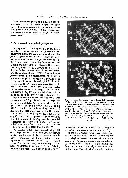
Among several transition-metal silicides, FeSi z may be a particularly interesting material for developing integrated optoelectronic devices. Its phase diagram shows an oe-FeSi, phase (tetrago- hal structure), stable at high temperature ( > 930°C) and certainly cc.~t aig,iJlg Fe vacancies. This ~-phasc lransforms flllo a / J -phase (orthorhombic s t ruc ture ) b e l o w ~ ~/50°C according to a ~ + Si. The ~-phase is stoichiomelric and transtorms into the a-phase above ~ 970°C [6] according to /3 ~ a + FeSi. These transformations induce a dramatic change in the electr ical properties of FeSi2; ~-FeSi~ is metallic whi le / j -FeSi~ is semi- conducting. The/3-phase is one interesting candi- date to establish a heterojunction on Si substrate. Its orthorhombic structure may he considered as a distorted CoSi 2 fec structure [6] whose epitaxy on Si has been extensively studied elsewhere 15].
Fig. ! shows schematically the crystallographic structure of/3-FeSi2. The (101) and (110) planes are good possibilities for lattice matching to ~he Si(l 11) face. The misfit is about - 5.3% along the Si[l l2] direction and + 1.4% along the Si[ l l0] direction for (10l) epitaxy on S i ( l l l ) , It is about - 5 . 5 % and + 2 % , respectively, for (110)epitaxy (fig. 2) on Si(l 11). For epitaxy on the Sit109) face, the (1(10) planes of /3-FeS1 z may be potential candidates. The misfit i~ then about + 1.4% (or + 2 % ) along the Si[ l l0] direction and + 2 % (or + 1.4%) along the Sill t0] direction (fig. 3).
As expected in this system whcrc / j -FeSi 2 (t01) or (110) planes, of twofold symmetry, are joined to the sixfuld symmetric Si(l 11) plane, each cpi- taxy is composed of three equivalent and equiprobable azimuthal or!entations (epitaxial variants) as schematically stt,3wn in fig. 2. The same phenomenon happens w~th the / j-FeSi z twofold symmetric (1001 plane in epitaxy on the
Fig. 1. Stick and ball models representing (a) CaF z strLcture af the melallic CoSi,; (b) orlhorhomhic slructure of the semicondu¢ling/3-FeSi~. ~-FeSi z structure can be ctmsidered a distortion of the CoS[~ cubic struc'.ure. In this case the [Ib(I], 11110] and [08I] directions of the CoSi z structure corre- spond to Ihe 11001. I(lll/and 11011 directions of the ~l-P~Si 2 structure, respectively. The lattice parameters are then: a(~- FeS~,) = 2 a ( C o S i , ) ; ht/3-FeSi z) = , t ~ - F e S i , ) = a/~2-tCoSiz); a = ~.863 .-~, b = 7.791 e~, , = 7,833 ~, "After
rot. 16].
Si fourfold symmetric (100) plane. Then two equivalent rotation twins may be observed (fig, 3).
In the past, several groups have investigated polycrystalline /3-FeSi 2 samples because the ma- terial displays interesting thermoelectric power properties [7]. Sample preparation was achieved by conventional mel t ing-cool ing techniques. From the intrinsic conductivity a bandgap of ~ 0.t) to 1 eV was deduced. More recently, Bust and

384
• . . . . . . - .-- /~% 7~<___
r - . k / x / < . . . ~1010i
:: : : : : :H::H:: C*rnrnon Ur,lt Meeh
98 ~2
(~l) t"eS;~(101)/Si~II1) wilh reSi:I010jfiSi<'lQ.
£ IX'~i,.'n ci aL / S e m i t ~ & w t m g sdi(tde silicon hetc, o~mwnlrcs
In order to prepare a single epitaxial /~-FeSi2 phase, one needs to carry out experiments under ultrahigh vacuum (UHV), avoiding the influence of impurities..Solid phase epltaxy (SPE) is a promising technique. It consists of an Fe deposi- tion at room temperature (RT) onto a clean Si substrate, followed by a subsequent annealing. If the SPE temperature is kept well below 900°C then the a-FeSi , phase does not form.
To our knowledge, few studies undci U H V conditions have been devoted to the FeSiz/Si
. v - v . , 7 ~ . ~ ~/-: . •
. : - - : 'x >/ . - .,':'-~: ," - >', " \ >-'k • +< t . . . . .
' , / -~ - \ . - " \ !" '1' ' I .1
Com~o~ Un;t ~esr, 4"3 .~2
(b) re$i:z{llO)lSi{111 ) wlih resi$oOq!!si.: lo-
Fig. 2. T~o ptv, slbilitics of matching planes of cpiloxial 13- FeSi 2 lln Sdlll). (at 15-[:cSi 2 (nil) plane Oll Sillll)• lb)
/J-Ft:Si 2111 a) plane on Sil I ! I ). t : St: + : fcSi 2.
Mahan [4] prepared thin films by furnace reac- tion of ion beam sputtered iron layers with Si wafers• They obser,'cd a probably direct optical gap of ~ 0.89 eV [8]. X-ray diffraction (XRD) showed a Iralycrystalline film. The first attempts to grow epitaxial films were undertaken by Cheng et al. [9]. Deposition of Fe under conventional vacuum conditions (at 10 -7 "]'off) with annealing in dry N= ambient or oil-free vacuum furnace, led to various iron silicide phases. Transmi.~ion elec- tron microscopy (TEML showed that B-FeSL, Oolycrystalline grains predominantly grew at ~ 60WC together with FeSi. The polyerystalline- to-epitaxial-FeSi, transformation was found to occur in the 9OO-ll~J°C :atlge where unfortu- nately ~0 and a phases coexisted.
7:1:7 : I
• " X N ~ ; L: . . . . . . .
C '~+~:n L:,':t '~e-',
( a ) FeSli(lO0)ISi(O01) with FeSi~lO]O]II$i<110>
:. "f-I: !}
-C
(b) FeSi~lO0)ISi(O01) w{th Fe$1:~OIOlllSi<lO0>
Fig. 3. Ltticc mulching of ~-FeSi2(lOO) epilaxlally gro~'n on Si(1O0). Two variaats have been nhservca. (3) /~-F¢Si=(I(]0) matcbing plane on Si(l~]) with /3-FeSiJ0]O] parallel to Si(llO). The lattice mismatch is Ihen + 1.4% or 2+0% dc- ~ending upon the alignment with either b or c (see fig+ I). (b) /3-FeSi2(la0) matching plane on Si(i011} with ~-FeSi z [011]]
parallel m Sit n}0). i : St; ~-: FeSi 2-

Z Derrten et aL / Semwouducting siliUde-silicon heWrm'rrlwmre~
interface. One may mention the investigations of Urano et al. [10] on RT Fe/Si ( I 11) and annealed F e / S i ( l l l ) interfaces with low-energy electron diffraction (LEED), Auger electron spectroscopy (AES) and angle-resolved photoelectron spec- troscopy (ARPES). Another work of Tanaji et aL [11] with LEED and AES was focussed on ultra- thin RT F e / S i ( l l l ) and Fe/Si(100) interfaces. No epitaxial fl-eeSi 2 phase was demonstrated by these authors. This was achieved for the first lime by Cherief et al. [12,13] on S i ( l l l ) and vicinal Si(itl0) faces followed by Mahan et al. [14] on Si(100).
2.L Epitax), o f fl-Fe Si e on Si( l l l )
The most widely used silicide preparation technique is the so-called solid phase epitaxy (SPE). whm'e one evaporates at first a metal layer (M) onto a clean Si substrate maintained at room temperature (RT). Annealing, under ultrahigh vacuum (UHV) conditions, this RT-M/S i inter- face at higher temp~raturc~ ('- 600~C) favou~ M and Si interdiffusion which induces the formation of various silicide compounds and sometimes MSi~ epitaxial growth on Si. Although silicide epitaxy can be achieved by this technique several drawbacks remain such as the presencc of twins. the high roughness at the surface and interface except on the nano-scale, and a large density of pinholes. The most influential parameters seem to be the annealing temperature, the initial M thickness and the initial Si surface morphology and cleanliness.
Several alternative epitaxy techniques have been introduced to remedy these disadvantages. They are molecular beam epitaxy (MBE), SPE with a Si cap before annealing, coevaporation of M and Si in the stoichiometrie ratio on silicon at RT and annealing, M deposition on a hot Si substtate, which is called reactive deposition epi- taxy (RDE), and finally the "template technique" [15], a two-step procedure where a well-con- trolled epitaxial template layer is first produced at low temperature, and then the thickness is increased via MBE performed at higher tempera- ture.
385
2. L / . Solid phase epita.ry o f ~-FeSi 2 on S i ( I l l ) We performed silieide formation in a RIBER
MBE chamber (base pressure ~ 10 m range). Fe was first evaporated onto atomically clean Si(I l l ) surfaces displaying (7 x 7) reconstructed super- structures, q'he Si wafers were two inches in diameter, chemically etched with the Shiraki m e t h o d [161, and t h e n t h e r m a l l y c l eaned ( ~ 70O°C) under UHV conditions with concurrent exposure to a Si beam [17]. With the substrates maintained at low temperature ( - 50°C), deposi- tion of very low Fe coverages (_< 2 ~,) leads to an initial slight intermixing between the Fe and the topmost Si atoms, forming an ultrathin transition layer where the local chemical environment of the Fe atoms displays characteristics of Fe in silicide. This bonding has been suggested previ- ously by various electron speetroseopies such as Auger [3] and photoemission experiments [18]
Y
/
[ \ ~ 4M.
- 5 o .5
E Er(eV) Fi 8. 4. Empty densily of stales above the Fermi level E F of room temperature Fc deposils on Siflll) as observed with bremsstrab[ung isuehromat spectroscopy. The spectrum of a fl-FeSi z standard is also included for comparison. The local chemical enviro[Imcnt of a I .~ Ee depoSil looks v¢,~/simitar to the .8-FeSi 2 one, while with increasing thickness it tends
towards the pure bulk Fe one. After roe IlSl.

3Sh
* . ",. "°° ~.o *°o ",° °~.
• 12.8 A~ •
. . . . . . ,
(at re(!~!)/s~O!l) ~;th r©lOhl~!s~oill
Fe<ll?,
t(3; streaks)
[ I t t 1 IS; streaks)
(b) The RHZED slteak plntetn ~-'tg 5 L~thcc m:tching of cp;t~xial I~c Fe film im SR l I ] ). tat I:g( I I I t pkluc on Sit I I I ). tb) Predicted RIIEt;D ~trcak pat loin along tall rna~¢~r azimulhs. Tile Si sllb~lt;~lc ~|te,~ ptai+
lions arc indicated I~ arrms~.
(fig. 4). Sla t t ing from this transition layer and increasing the Fe coverage one observes the cpi- taxial growth of an almost pure race Fe layer as testified by R H E E D . The epitaxial relationship is: matching planes bee Fe(l l 1)tlSi(I l 1) with azimuthal orientation bee Fe[ 110] IISi[110].
The lattice mismatch is then about 5.7% {fig. 5) if one compares twice the Fe parameter (a = 2.87 A) to that of Si (a = 5.43 Pt). This epitaxia[ Fe growlh on S i ( l l D has also been confirmed with ex situ X-ray diffraction (XRD) [19], Ruther-
ford backscattering (RBS) and ion channeling IIC) measureht,~nts [21)].
For very. thin Fe layers (_< It) ,~), the surfaces seem :o be rather smooth since reflection high- ener,,~, electron diffraction ( R H E E D ) patterns displayed nice streaks, while for thicker films the epitaxial growth is still conserved but the Fe surfaces become very rough and transmission-like R H E E D spots were observed. Development of the surface roughness during MBE growth at low temperature is an intriguing and fascinating prob- lem and needs more detailed studies [21,22],
In order to achieve SPE o l ~-FeSi • on St(111). the as-deposited Fc/Si couples ,.yore brought to
61HI°C with heating rates from I to 5~C/min. R H E E D pattern images were recorded in re~l time with increasing temperature and stored in a computer. Diffi'action streak and spot intensities itfld lattice spacings were then measured from these images. Depending upon the initial de- posited ICe thickness, the interaction during heat- ing adopts quite different bchaviours. More de- tails may be found elsewhere [23]. Here we illus- trate •nly one kind of the evolutionary develop- ment with annealing, correspoudlng to an initia!!y ~ 311 A thick Fe htyer.
Fig. 6 shows the R H E E D intensity evolution with annealing temperature. After the R T Fc deposition. R H E E D spots of a rough epitaxial Fe layer are observed. Increasing the temperature (to ~ 20O°C) results in a smoothing of the Fe ~,urfacc layer us shown by the elongation and conversion of the Fe R H E E D spots into Fe R H E E D streaks. No Fe -S i intermixing was ob- served by Auger depth profile analysis [24]. X R D measurements confirm the absence of Fe -S i in- tcrdiffusion at such a low temperature and X R D spectra still display only features of an epitaxial bcc Fe thin film [19]. The same result has been found with RBS and IC techniques [201 while scanning electron microscopy (SEMI reveals a uniform surface without asperities at least within the - 100 .~ SEM lateral resolution.
At about 250°C the Fe R H E E D intensity sud- denly decreases. A Fe -S i intcrdiffusion occurs throughout the film. as observed with Auger depth profiling [24]. The chemical composition is very close to that of the FeSi. X R D confirms also the

£ Derrk'tl c/oL / SemR'otldltctittg Mlit'idv-~ihco/t heteloxgrucfun,s 387
I,,,, Fe no thll~acli0n • : " 58 80 -~ I~ ~FeSi 2
- 6 5 •
~ ...':"'~ik " " " :
i I I I !
T~2SOC ~ o o o'® t dl R ~' ,%
d T . . . . . . . a- i a 'a ' l '~ L I
I I I I I I0~ 20~ ~nO 4QO 5010
lemperalure tO) Fig. 6. RHEED intensily evolution with annealing tempera- ture. Onb' Fe diffracaon is observed after 30 A Fe deposition at room lemperature trap panel). A sudden Fe RHEED disappearance nlccurs at ~ 251FC and then /]-FeSi z diffrac- tion appears at ~ 45(FC. Bottom panel shows the derivative versus temperalure o~ RHEED intensity, e: Fe diffraction;
m: ~-FeSi2 diffractitm.
formation of the FeSi compound since diffraction peaks of a polycrystallioe FeSi film were observ- able [19]. Fe-Si intermixing was also found with RBS and IC [20]. We should note that this FeSi formation temperature depends ~omewhat upon the initial Fe layer thickness (250°C for a 30 ,~ thick Fe layer, 380°C for a 1200 ,~ layer) but is always marked by the complete Fe RHEED pat- tern disappearance. An Auger depth profile anal- ysis, performed on a 1200 A thick Fe layer, ther- mally quenched just before and after the com- plete Fe R H E E D pattern disappearance shows that this effect is correlated with the massive diffusion of silicon into iron. When this massive
Si diffusion takes place the whole film is strongly perturbed structurally. Indeed SEM images re- veal that Si diffusion is dearly associated with tile formation of large holes in the FeSi layers [23].
With further increases in temperature only the diffuse RHEED background could be observed until ~ 450°C, At this temperature a new and complicated RHEED pattern appeared, Careful analysis of the pattern along the main azimuths of the Si substrate showed that the new epitaxial phase is j6-FeSi~ ( ~ 100 A thick). Diffraction streaks of three different epita!:ial variants are obsel'ved confirming one or both of the following epitaxial relationships: - matching planes
~-F~Si2( I,°, | ) II Si(I l l) with azimuthal orientations #-FcSi 21010] II Sit011 }
- matching planes fl-FeSi 2 (110)[ISi(] 11) wi'.h azimuthal orientations ,6-FeSi~ [001]llSi{011}
As previously predicted, XRD measurements confirm these epitaxial growths. The XRD-mea- sured interplanar spacing is close to the one that we expect from buik crystallographic ~Jr, sidera- lions. It suggests that there is little or no elastic strain of the ~ 100 A thick/~-FeSi 2 epilayer. The limited XRD instrumental resolution does not allow to determine if only one matching face occurs (.6-FeSi2(101) or ( l l 0 ) plane) [25]. This has been solved by T E M and TED experlmcnts. T E D was performed along both Si[l l0] and Si[211] directions in a cross-section view [26]. ~oth epitaxial (161) and (110)/~-FeSi 2 planes are found to grow paralleZ to Si(I I 1) ones. SPE tech- nlque usually shows that cpitaxy deteriorates badly with thickness. Indeed very recently we grew by SPE a very thin film of fl-FeSi 2 ( ~ 60 A) with a controlled rough surface. Transmission RHEED then could be performed and showed only the (101) fl-FeSi 2 epitaxy. The correspond- ing lattice image indicates that the crystalline quality of the film is locally very good and the FeSi , -Si interface very sharp at atomic mona- layer scale as previously reported [12,13].
The chemical composition of the phase formed

388
at temperatures hi~her than 450°C, checked with RBS and Auger elect.on spectroscopy, is that of FeSi.,. h is also interesting to note that the 451FC p-FeSi , Formation temperature fits nicely the amnrpbous-crystalfine /3-FeSi, transformation one as seen previously in thicker polyc~,stallioe films [2"/,28]. During SPE annealing, the p-FeSi 2 RHEED pattern remained tmehanged in the 450-f',I10°C range as also previously found with LEED [12]. It has been recently suggested that at higher temperatures the fl-FeSi~ layer is covered with an St-enriched topmost layer [29] as in the ease of CoSt, on Si l l I I ) [311].
F-x situ optical measurements were performed on these cpitusial / /-FeSi, films and an absorp- tion coefficient a in the range 194-105 cm ' was found at a photon energy of ~ 0.85 eV, in agree- meet with measurements on thicker polycrys- talline layers [4.81. An ~-' versus phnmn energy pint shows a linear variation suggesting a direct optical gap of ~ 0.84 and ~ 0.88 eV at 3110 and lfi K. respectively 119]. These values are in ap- proximate agreement with those obtained previ- ously by Lefki ct al. [311 ( ~ 0.85 eV at 300 K) and also by Mahan et al, [4,8] on thicker films ( ~ 0.89 eV at 3110 Kk The semiconducting nature of ~q-FeSi, bus bee.a revealed recently by self-con- sistent calculations of the band structure per- formed by Christenscn [32] who also finds a value c,. ~ about - 0.8 eV.
Measuring both the occupied and empty states of fl-FeSi z films with in sitn X-ray photocmission spectroscopy tXPS) and bremsstrahlung isochro- mat spectroscopy (BISL De Creseenzi et al. [18] deduced a gap value of about 1 + 0 2 eV (fig. 7). Another in situ gap measurement on a very thin .a-FeSi, film has been performed with high-reso- lution electron energy loss spectroscopy (HREELS) by Rizzi et al. [33]. Fueh-Kliever surface phonous have been observed at low-en- ergy excitation spectra (loss at ~ 50 meV) sug- gesting the semicondoeting character of the FeSi z film. Moreover in a higher energy excitation range a broad 1o~ structure occurs at ~ 0.8 eV corre- sponding to a direct intcrband electronic transi- tion.
Very recently with oar SPE-grown thin films ( ~ 20t;0 ~ thick), of lesser structural quality pbo-
] 12t.rhen ¢1 at. / St'l~dc~mdtlettng silk'idt.-.~illc¢~l hett'r~trnctltres ~~I' xn' . , s
1 '
- l O - s n 5
t - i f lea} Fig. 7. {-~mpalison belween XPS and BIS speclra of a/3.FeSi., tilrn and tt~lal densities of stales ealcululed by Christensen
[32]. After tel. 1181.
tolumineseence signals have been observed at 2 K [34]. Two photoluminescence peaks, with full width at half maximum ranging 15-20 meV, are located at 0.795 and 0.839 eV, respectively. They compel a belief in the direct nature of the gap and suggest potential integrated optoelectronic applications for this material. The photolumines- eence experiments described bere are in agree- ment with those obtained by Dimitriadis et al. [35] on thicker polycry~iailhl¢ samplc~.
2.1.2. Reactice deposi t ion epitaxy o f f l -FeSi 2 on S i t / H )
SPE growth of/3-FeSi., provides ¢pitaxial films only for initial Fc thickness lower than ~ 300 A. Above this value the compound remains fl-FeSi z but the film becomes polycrystalline. Obviously, a competition between diffusion-controlled and nu- cleation mechanisms occurs. Thus¢ mechanisms arc also complicated by amorpbous-e~stall ioe transitions. In order to remedy these drawbacks we have applied the RDE technique to grow FeSi 2, evaporating Fe atoms directly onto Si hot substrates. In addition to the final orthorbombic .8-FeSi 2 phase, usually obtained at growth tem- peratures higher than - 500~C, it was possible at lower temperatures and small Fe thicknesses (few tens of A) to grow some other epitaxial and obviously strained phases such as a CaF2-strue- ture-fike FeSi 2 compound and an epitax~al FeSi

J. I&,rriaa et aL / SoniconductiJIg silicide-silicon heterostn~cmres
compound, both of which deserve tu be investi- gated in more detail [36].
Another interesting result fur RDE deals with the limiting thickness of epitaxial /~-FeSi z, RDE provides us with thicker epitaxial films as com- pared to SPE. RHEED streak patterns could be obse;.ved with films as thick as ~ 2000 /~. The films in these cases are formed with large grains ( ~ ~m size) separated by holes. All other physi- cal properties as measured by XRD, RBS, XPS, Auger and optical characterization reflect faith- fully the ~-FeSi 2 semieondueting nature.
2.2, Epitaxy o f ~-FeSi 2 on Si(lO0)
The first evidence of successful ~-FeSi~ epi- taxy on Si(100) was demonstrated by Cherief ct al. [12]. These authors used vicinal Si(100) faces in order to favour epitaxial growth. The Si(100) surfaces were misoriented by 5 ° towards the [110] direction, resulting in bilayer step edges which are parallel tu the [111] direction. The width of the (100) terraces is then about ~ 31 A which should correspond to four unit cells of ~-FeSi2(100) planes (see section 1).
LEED, Auger and photoemi~sioo spectroscopy of SPE thin films have already been published elseccherc [12,37] and confirmed ,t:.=, 7xg'ected epitaxial relationship: - matching plane
/3-FeSi2(100) II Si(100) with azimu.thal orientation /3-FeSiz[010] and [001] IlSi( 110}.
Similar results were also obtained by Mahan et al. [14] by RDE at ~ 5fl0°C in a MBE machine. On plane Si(100) faces, these authors achieved the epitaxial growth of thicker ¢-FeSi 2 layers displaying very nice RHEED patterns which could he explained by the previous epitaxial relation- ships. The surface morphology was rough due to islanding which always preceded the formation uf a continuous film. In an effort to obtain smoother films, MBE and SPE wer~ investigated by these authors [38] who combined both techniques when following the template method [15]. They first co-deposited Fe and Si at stoichiometri¢ ratio I : 2, at temperatures lower than 200°C and subse-
3S9
quently annealed to 300°C to obtain an initially smooth epitaxial disilicide which quite surpris- ingly followed another epitaxial relationship: - matching plane
~-FeSi2(100) IISi(101)) but with azimuthal orientation /~-FeSi 21010] and [0111] II Si( 100),.
If the above SPE deposit ion/anneal pruee.. durc was carefully repeated several times, the excellent R H E E D streak pattern was preserved, suggesting a very smooth and speculatly reflecting surface. The microscopic mechanisms of this pe- culiar epitaxial growth are not still fully under- stood.
Recently the SPE technique was applied by Alvarez et al. [291 to reconsider FeSiz growth on Si(100). These authors found with increasing tem- perature a sudden drop of the XPS core level intensity ratio F e / S i at ~ 350~C, signalling the onset of the reaction of silicide formation. T';,o plateaus were observed, extending from 430 to 550~C and from 600 to 800°C, respectively. They reflect the formation of FeSi and FeSi 2, similarly observed on Si(l 11) but at slightly higher temper- ature, probably due to difficulties in precisely measuring surface temperature rather than to difference of crystalline surface orientation. In- tcic~tlng scanning tunnsl!~g .~llcrosco~y (STM) pictures revealed a rather inbomogencous film with a tendency towards epitaxial growth favoured by the presence uf surface steps of the Si sub- strate. Murcuver a small amuunt of Si was de- tected at the outer surface by ion baekseattering spectroscopy.
3. Ep i taxy u f u t h e r semiconducting silicides o n Si
Among all the other known semiconducting silicides (ReSi2, CrSi2, Mn,5Si26, lraSi 7, OsSi 2) only two of them, besides the /:~-FeSi 2 already extensively discussed, have demonstrated epitax- ial growth on Si.
ReSi 2 and CrSi 2, whose band gaps are ~ 0.1 and 0.3 eV respectively, both probably of indirect nature, have attracted recently much attention [38-45]. Under UHV conditions, Mahan et al.

[39] achieved cpitaxial gi~o;vth of ReSi 2 on St(IIHI) with the R D E tuchnique. Highly oriented films wcrc obtained as testified by R H E E D , T E D , TEM, XRD and ion channeling observations. All excellent channeling yield exhibiting a mini- mum of 2% was obtained for a growth temper- ature of ~ 650~C. ReSt 2 is orthorhombic and the predominant hctcrocpitaxial relationship is ReSt,(010) II Si(C~I ) w-ith RcSi2[001 ]II S i ( I I0). e r r ing to the symmetD' difference hetv ,cen opt- layer and suhstrat¢, the films are composed of two t)0~ rotated epitaxial variants in a similar fashion to B-FeSi , on Si(l~lll. The R D E tech- nique produces film surfaces which are rather rough; indeed, beautiful T E D patterns were ob- tained with conventional R H E E D instrumenta- tion, in situ. On thicker pol.~,'cD, staliine ReSt 2 f i l~s spectral transmittance and rc f icctancc mea- surements along with the temperature depen- dence of the conductivity suggest that the band gap is of indirect nature and is approximately 0,12 eV. A direct t, 'ansilion at ~ 0.36 eV was also observod [40]. More details on the growth and properties of RcSia can be found in refs. [38,39],Thc epitaxia[ tendency of ReSt , on Si(~01) seems to he vcD' persistent. This is revealed by the response of an cxpitaxial film to ion beam amorphization and subsequent annealing treat- ments. A film which was rendered "'X-ray amor- phous" regained its 2% channeling yield after a brief anneal at 90g°c. This result indicates a real potential for SPE for obtaining cpitazial films with improved surface morpho logy°
The quest for epitaxial CrSi 2 films, another narrow bandgap semiconductor, has attracted more attentinr, than that of perhaps any other scmiconducting sillcidc [41-45]. This effort was encourag'~, by a promising theoretical lattice match of the hexagonal CrSi 2 basal planes to the S i ( l f l ) face which has a possible common unit mesh of 5 l ,~2 with a mismatch of ~ 0.3% [45] (fig. 8). According to ref. [45], CrSi 2 film was grown by R D E with the Si substrate maintained at 600°C. A post-growth anneal at 90WC did not alter the epitaxial relationships of the as-grown film bu t brought forth the highest quality R H E E D patterns in t e rm of streak sharpness and bright- ness. Analysis of very sharp R H E E D streak pat-
J i)ertietl ¢t IlL / $valitvtidutting Mtwidc-silic¢m hetetowrot'lures
. ÷ . + ° . + . .
S;litOl ' " . ~ ~ CrS~lto~o I
(a) Type A: CrSi~(O001)/$[(l~l)
with Cr Si2( %OiO)[]Si< 1 I{1>
. ' , * . *. t # ,* . * . * , ¢, • t
-1.2% w * ~ - . . . . . . , . • ~ . . . . . , .
• , . . . . . . . . . . . ¢ ° . • ° . . • . • . •
612 ~2
(b) Type a: CrSi~(~OO/Si(Ut)
wilh CrSi20120)1~Si<110>
Fig. 8. Lattice malchlng of hexagonal CrSi 2 on St(Ill). Two types of eplt;~x)' hate hucn ubsc~¢d and may be explained as: (a) CrSi, ( f, fflO 1 ) parallel In Sit I I I ) with CrSizll0/a ] pard e 0 Si(tl0): (b) wilh CrSi_.[I l_~a] paralh:[ to Si(II0), Atler ref.
1451.
terns, cross-checked with several azimuths, allows a eoalplete specification of the epitaxial relation- ship, which is matching plane CrSi 2(0001) ]}Si(I 1 l ) with azimuthal orientation CrSi2(10]0) [jSi(110), as expected for the above-stated lattice matching. The CrSi 2 hexagonal surface unit mesh is rotated by 30 ° with respect to that of St.
R H E E D also revealed the presence of limited film regions of a competing azimuthal orientation CrS i2 [ l l20 ] l JS i ( l l 0 ) (fig. 8). It is not presently understood why the competing orientation occurs

J. Derrieu e¢ at. / Semiconducttng siltt'id¢-~iliton hetero~trttctl~n,s
at all since its lattice matching is not nearly as favourable.
With eoevaporafion of Cr and Si in their stoi- ehiometrie ratio on Si(l l 1 ) maintained at ~ 45fl°C it is also claimed that it was possible to favour only one azimuthal orientation (the rotated CrSi z unit mesh)[44]. During the initial stages t)f growth epitaxial CrSi has also been reported [44].
The semicondueting properties of thick and polyerystalline CrSi., films have been previously studied [46-48]. A probably indirect gap of ~ 0.3 eV was found, suggesting potenlial applications in integrated infrared photodetectors.
4. Summary and prospect:,
4. L About growth techniques
Various epitaxy techniques (SI'E. RDE, code- position + SPE, M B E , . . . ) have been applied to grow epitaxial semieonducting silicidcs. At first glance they seem to offer an easy way to get epitaxial films, to study in situ diffusion ,rod ,u- clea!ion mechanisms in the solid state, structural and electronic properties of amorphous-crystal- line phase transitions at surfaces and interfaces of thin films. However all of them bear intrinsic drawbacks leading to various defects of the films. For example SPE has a strong tendency to render poi'~,cr~stalfine the layer, limiling the ep~taxial thickness, while RDE creates rough film surfaces as a result of the tremendous alnount of silicon transport required. The alternatives include MBE and codeposition + SPE which improve film mor- pholog~ i f stoiehiomctry is respected during de- position. The latter technique might be promising in the light of several works which demonstrated the epitaxial regrowth of films previously amor- phized by ion implantation. These experiments have been performed on ReSi z [49] and also on O-FeSi, where Oostra et al. [50] achieved the growth of epitaxiul layers buried in Si substrates (mcsutaxy). Mesotaxy has also been applied to grow buried epitaxial CrSi.~ in Si [51].
In order to render the growth of silicides com- patible with Si device technological processes, but still keeping all the advantages of previous physi-
391
col deposition techniques (UHV environment, cleanliness, in situ R H E E D , . . . ) chemical vapour deposition (CVD) at very low pressure should be developed. The chemical deposition technique has several advantages such as high flexibility and uniform and selective deposition over large sub- strate areas.
The first step in CVD is to search for gas precursors which could deposit the transition metal with Si via a decomposition process in- duced by an external energy source (temperature, photon or electron irradiation, . . . ) . For example. metal carbonyls have been used to dcposlt pure metal layers [52,53], and silane to homoepitaxially grow Si [54,55]. Silieides have also been fabri- cated with metattoceuc and silane in a CVD reactor at atmospheric pressure [56]. These au- thors achieved the growth of fl-FeSi z on Sit100) and S i ( l l l ) m~soriented by 3 ° off towards the [ l l0] axis. They used a pulsed growth technique, s~nding separately and alternativcl~ during the growth each gas precursor (ferrocene and silane) into the reactor chamber. The growth tempera- lures wcre between 750 and 900°C. Epitaxial films up to ~ 1 ,o,m thickness were obtained on Sit111) as testified by XRD. Photolumineseence spectra at 2 K confirm the semiconducfing nature of the material where two sharp peaks have been ob- served at 0.797 and 0.837 eV. In the light of these results, we consider the use of gas sources at very low pressure in eonvemional MBE chamber to be quite promising, fulfilling both fundamental and applied demands.
4.Z About epitaxial relationships and t'aHous az- imuthal orietltatioas
Epitaxial variants ("forced" twins with equiva- lent azimuthal orientations) are expected when- ever the symmetry of the substrate is higher than that of the epilayer. The S~(IlI) and (100) faces are sixfold and fourfold symmetric, respectively. The corresponding B-FeSi z matching forces are the twofold symmetric (110), (101) and (100). This is the reason why one finds three and two fl-FeSi 2 equivalent azimuthal orientations on Si(l I 1) and (100), respectively. The same behaviour is fol- lowed by ReSi 2 on Sit100).
392
More surprising are the two competing orien- tations of hexagonal CrSi, layer epitaxially grown on SKil l ) . This intriaguing problem calls for more detailed studies in the future.
In order to get a single-cJ3,sial film one must reduce the substrate surface symmetry. A Sill 10) face possc~es twofold s~Tnmetry bat unfortu- nately there does not appear to be a good lattice matching.
As an alternative one might explore ways to lift the oriemational dcgeneraq,' of the St(001) and (I I I ) faces. One might, for example, slightly misorient the Si substrate (to form vicinal faces). A slight miscut angle off the direction normal to the substrate can sometimes result in a regulan array of surface steps separated by terraces. It is probable that the stepped surface would favour one of the equivalent epitaxial variants if codepo- sition is used. On Si(0Ol) another approach worth exploring would be to grow the films in a single- domain (2 x 1) reconstructed Si(Ct01) surface, i t might also be possible to create a state of uniaxial strdin in the Si substrate with an array of thermal s i n 2 strips.
4,3, Aboot potential applications o[ semieondncting silicides
To achieve the long-term goal of making semi- conducting silicides available for the development of r, ovel integrated optoelectronic devices, it is ncces.sary to demonstrate epitaxial films of a quality suitable for such device development. We believe that in the near future tremendous progress will be made because many groups around the world have begun to put their effort into the semiconducting silicide field.
It is worth mentioning that although the group of semiconducting binary silicides offers numer- ous choices for the lyandgap energy, from large bandgap materials such as CazSi (1.9 eV) and OsSi., ( i .8 eV) to smaller ones such as ReSt , (0.12 eVL it might be worthwhile to ted to "'tailor" tile electronic properties to the need. We are suggesting that one may enlarge those band gap energy choices by developing the bandgap engi- neering of semi~nducting silicides, mixing for example, when possible, two binary silicides to
£ D~vricn et aL / St-mk-m:d,tcting ~ilitide silicon h¢tcroslrteffllre,
form a pseudobinary compound [57] with the desired latrine parameter and bandgap energy, following the way opened for I I I -V and II-VI compounds several years ago.
Acknowledgements
This work is financ Aly supported by the EEC through the ESPRIT ~,asic Research Action No. 3026. Grants fl'om the French Minist/:re de la Recherche et de la T,'chnologie are also grate- fully acknowledged (c ~atraet No. 88 R 0973 and
S 0249). Our unde~ ,tanding of these topics has :.;r,atly improved thanks to fruitful collaborations with the groups of Profs. M. De Crescenzi, J.F. Petroff, R. Miranda, S. Lagomarsino, J.P. Andr6 and A. Van Oorkum.
References
II] B.Y. Tsaur znd G.M. Metz¢. Appl. Phys. Lett. 45 (1984) 11117.
[21 R. Zachal, K. EberL G. Abgtr¢iter, E. Kaslmr and H. Kibbel. Phys. hey. Lye. t~4(igga) 1055.
[3] See a review paper h~: J. Derrien. J. Chcvrier, A. Younsi. V. Le Thanh and J.P Dussaulcy. Phys. Szr. (1991), in pxess.
[4] M B~lst and J.E, Mahan, .i. Appl. Phys. 58 (1985) 2696, and references Iherein
(5| See a review paper fly: J. Dcrrien and F. Arnaud d'Avitaya. J. Vac. Sci. ] echnoL A 5 (ItJ87) 21 ] I; see also ref. [12].
i6i Y. Dusausoy. J. Prola~ R. Vandii and B. Roque•, Aeta Cryst. B 27 (1971) 12(/*
[7J U. Birkholz ~nd J. Sc~;L'hn. Phys. STatus Solidi 27 (1%8) 413.
{8] M.C. Bost and LE. Ma:aan, .i. AppL Phys. 64 119881 203,~. [9] H.C. Cheng, T.R. Yen and LJ, Chen, AppL Phys. Len.
57 (1~85) 5246. {lo} T. Urano, T. Ogawa, T Kanai i and F. Fujimoto, J Vac.
Sci. TechnoL A 5 (1987) 2046. [11] T. Tanaii, T. Urana, A. Hiraki and M. Iwami, in: Proc.
8th Int. Vacuum Congxess, Cannes, 1980, VoL I, p. 117. [121 N. Cherie[. R. Cinzl. M, De Crescenzi, I Derrien, T.A.
Nguyen Tan and J.Y. Veuillen. AppL Surf. Sci. 41/42 (1989) 241.
[13] N. CherieL C. d'Anterroches. R. Cinti. T,A. Nguyen Tan and .I. DerTien. AppL Phys. Left. 55 (1989) 167.
[14i .I.E. Mahan. K~M. Gcib. G.Y. Robinson. R.G. Long, Y. Xinghua, G. BaL M.A. Nicolet and M. Nathan. AppL Phys. Left. 56 (1990) 2126.

Z DerHert et al. / S,~micoltductiltg sificfde-sillcon helerostrllclures
[15] R.T. Tung and J.L, Bal~tone, Appl. Phys. Lett, 52 {1'488) 1611.
[16] A. lshizaka and Y. Shiraku. J. Electrochem. Soc. 133 ( 19861 666.
[17] K. Kugimiya. Y. Hirofuji and N, Matsuo. Jpn. J, Appl. Phys. 24 11985) 564.
[18] M, De Crescenzl. G. Gaggioti, N. Mozta, F. Patella. A. 1]alzarotti and J. Derrien, Phys. Rev, 13 42 (1990) 5871.
{19J S. Lagomarsino, private communication. [20] M.G. Gtimaldi and D. Oil~tra, private communicatinn. [21] D.E. Wolf and 3. Villain. Eu~phys. Lett. 13 (ITS0) 389. [22] D.J. Eaglesham. J.J. Grosman and M. Cerullo, Phys. Rev.
L¢II, 65 11990) 1227. [23] J, Chevrier, V. Le Thanh. S. Nilsche and J. Derrien.
Apph Surf. Sci. 56-58 (I992) 438. [24] F. Arnaud d'Avilaya, private communication. [25] S. Lagomarsino. F. Scarinci. C. Giunnini. P. Caslrucci. G.
Savelli. J. Derriun. J. Chevrier, V. Ix: Thanh Vinh and M.G. Grimaldi. J. Vac. Sci, Technol., in press.
126] Y. Zheng, private communication. J271 S.K. Sharma. W.A. Theiner arid H.P. Geserich. Phys.
Stalus Solidi (a) 25 (19741 K65. I~ l M. Michelini. F. Nava and E. Galli. J. Mater. Res. (1991),
submitted. [21)] J, Alvarcz, J.J. Hinarcjos. E.G. Michel, J.M. Gallego.
A.L. Vasquez de Parga. J. de La Figueiro. C. Ocal and R. Miranda. Apph Phys. LelI., in press.
[30] G. Oew~nner, C. Pirrl. J.C. Pl:ruehelli, D. Bolmont, J. Derricn and P. Thir/, Phys. Rev. B 38 (1988] 1879.
[31] M, Lclki, P. Muter. N. Cherief and R. Cinti, J. Appl. Phys. 69 (1991) 352.
[32] N.E. Chrlstensen, Phys. Rev. B 42 (1990) 7148. [33] A. Rizzi. H. Moritz and H. Luth. L Vac. Sei. Technot, A
9(1991)912. [34] J.N. Patillon and J.P Andre, prlvale communication. [35] C.A. Dimitriadis. J.H. Werner. S. Logothelidis, M. Stulz-
mann, L Weber and R. Ne~per. J. Appl. Phys. fi8 (1990) 1726.
[3fi] L Chewier, V. Le Thanh and J. Derrien, unpublished.
[37) S. Kcnnou. N, Cherier, R. Cinti and T.A. Nguycn Tan. Surf. Sci. 211/212 (1989) 685.
[38] K.M. Geib, J.E. Mahan, R.G. lamg, M. Mathtn and G. Bai, unpublished.
139] J.E. Mahan, K.G. Gcib, G.Y. Robin~m, R.G. Long, y . Xingbua, (3. Bai, M.A. Niet~l¢l and M. Nathan, AppL Phys. Lett. 56 (1990) 2439; G. Bai. N. Nicolgt, J. Mahan and K. Gelb, Phys. Roy. B 41 (1990) 8603.
[40] R.G. Long, M.C. Bosl and J.E, Mahan, Thin Solid Films 162 (1988) 29.
[41] V.G. Lifshits. V.G. Zavodlnskii and N.I. Phyusnin, Phys. Chem. Mcch, Surf. 2 (1984) 784.
[42) F,Y. Sbian. H.C. Cheng and L,J. Chen, J. Apph Phys. 59 (1986) 2784.
[43] R.W. Fathauer, P.J. Grunthaner, T.L. Lin, K.T. Chang, J.H. Mazur and D.N. Jamlerson. J. Vac. SeL Tcehmd. B 6 (198h) 7()8.
[44] L, Iladerbache. P. W¢lz¢l, C, PirrL J:C. PeruchettL D. Bolmonl and O. Oewinner, Surf. Sci. 209 (1989) L139.
[45] J.E. Mahan. K.M. Oeib, G.Y. Robinson, G. Bai and M.A. Nieolel, J. Vac. S,,:i. Tcchnol.. in pre~,
[46] I. Ni~hlda and T. Sakata, J. Chem. S~lids 39 0978) 499. [47] F. Nava. T. Tien and K.N. Tu, J. Appl. Phys. 57 (1985)
2018. [48] M.C. Bost and J.E, Mahan, J. AppL Phys. 63 (1988) 839. [49] K. Kim, G. Bai, M. Nieolet, J. Mahan and K. Geib, AppL
Phys, Let1. (1991), in press. [50) D, Ooslro. private communication. [51) A.E. White, K.T. Short and D.L Eaglesham, Apph Phys.
Lull. 56 (1990) 1260. [52) G.J.M. Dormans. J. Cryst. Growth 108 (1991) 806. [53] R.B. Jackman and J.S. Foard, Surf. Sci. 209 (1989) 151. [54] B.S. Meyer~n, Appl. Phys. Let'.. 48 (1986) 797. [55] H. Hirayama, T. Tatsumi, A. Ogura und I'4. Aizaki. Apph
Phys. Lelt. 51 (1987)2213. [56] 11. Alaoui, J.N. Patillon, C. Schiller and J.P. Andre, 4th
European Workshop on MOVPE, Nijmegen. The Nelherlands. June 1991. Io be publishetl.
Copyright © 2022 FDOKUMEN