Erbium Silicide Growth in the Presence of Residual Oxygen
26
Erbium silicide growth in the presence of residual oxygen Nicolas Reckinger, a,z Xiaohui Tang, a Sylvie Godey, b Emmanuel Dubois, b Adam Łaszcz, c Jacek Ratajczak, c Alexandru Vlad, Constantin Augustin Duţu, and a a Jean-Pierre Raskin a a ICTEAM institute, Université catholique de Louvain (UCL), Place du Levant 3, 1348 Louvain-la-Neuve, Belgium b IEMN/ISEN, UMR CNRS 8520, Avenue Poincaré, Cité Scientifique, 59652 Villeneuve d’Ascq Cedex, France c Institute of Electron Technology, Aleja Lotników 32/46, 02-668, Warsaw, Poland z E-mail: [email protected] 1
-
Upload
independent -
Category
Documents
-
view
1 -
download
0
Transcript of Erbium Silicide Growth in the Presence of Residual Oxygen

Erbium silicide growth in the presence of residual oxygen
Nicolas Reckinger, a,z Xiaohui Tang,a Sylvie Godey,b Emmanuel Dubois,b Adam Łaszcz,c Jacek
Ratajczak,c Alexandru Vlad, Constantin Augustin Duţu, and a a Jean-Pierre Raskina
aICTEAM institute, Université catholique de Louvain (UCL), Place du Levant 3, 1348 Louvain-la-Neuve, Belgium bIEMN/ISEN, UMR CNRS 8520, Avenue Poincaré, Cité Scientifique, 59652 Villeneuve d’Ascq Cedex, France
cInstitute of Electron Technology, Aleja Lotników 32/46, 02-668, Warsaw, Poland
zE-mail: [email protected]
1

The chemical changes of Ti/Er/n-Si(100) stacks evaporated in high vacuum and grown ex situ by rapid
thermal annealing were scrutinized. The emphasis was laid on the evolution with the annealing
temperature of (i) the Er-Si solid-state reaction and (ii) the penetration of oxygen into Ti and its
subsequent interaction with Er. For that sake, three categories of specimens were analyzed: as-
deposited, annealed at 300 °C, and annealed at 600 °C. It was found that the presence of residual
oxygen into the annealing atmosphere resulted in a substantial oxidation of the Er film surface,
irrespective of the annealing temperature. However, the part of the Er film in intimate contact with the
Si bulk formed a silicide (amorphous at 300 °C and crystalline at 600 °C) invariably free of oxygen, as
testified by x-ray photoelectron spectroscopy depth profiling and Schottky barrier height extraction of
0.3 eV at 600 °C. This proves that, even if Er is highly sensitive to oxygen contamination, the
formation of low SBH Er silicide contacts on n-Si is quite robust. Finally, the production of stripped
oxygen-free Er silicide was demonstrated after process optimization.
2

In the recent years, the continuous trend to device miniaturization continuously requires the introduction of
additional elements from Mendeleev's table in complementary metal-oxide-semiconductor (CMOS) technology,
for instance, rare-earth (RE) metals. RE oxides1, , ,2 3 4 and silicates5 find application as gate dielectrics because of
their high relative permittivity. On the other hand, RE silicides are materials of interest for the formation of
ohmic or low Schottky barrier contacts over lowly doped n-type Si substrates. They are indeed known to present
the lowest Schottky barrier heights (SBH) to electrons, amounting to 0.27-0.28 eV.6, ,7 8 In that context, the RE
silicides are particularly attractive for source/drain contacts in Schottky barrier metal-oxide-semiconductor field-
effect transistors (SBMOSFET)9, ,10 11 and as materials for infrared detectors.12
RE metals are highly prone to oxidation because of their high affinity for oxygen,13 useful property for the
formation of oxides and silicates. However, the formation of one of these compounds is often accompanied with
the formation of the other(s). For instance, RE oxides are prone to transform into silicides or silicates after the
unavoidable high-temperature annealing in standard CMOS technology, a source of degradation in the
dielectrics. Conversely, RE silicates or oxides are readily formed during RE silicide growth, which can be
detrimental to the silicide resistivity and to its SBH on n-Si since a very small oxygen content at the interface
with Si causes a substantial SBH rise.14 A first possibility to avoid oxidation is to perform the Er-Si solid-state
reaction in ultrahigh vacuum (UHV) conditions.6, ,15 16 That method is very suitable to fundamental studies but
less appropriate to industrial applications. To relax the constraints on the fabrication of RE silicides, several
groups proposed to cover REs with a capping layer (one-shot deposition without breaking vacuum) and to grow
the silicide by ex situ annealing.8, , ,17 18 19
In this article, we propose to scrutinize the chemical changes of thin erbium (Er) films deposited under high
vacuum conditions on Si in the presence of residual oxygen after ex situ thermal treatment by x-ray
photoelectron spectroscopy (XPS). The objective is first to investigate the penetration of oxygen into the stack
and to determine which reaction predominates at the interface with Si. It is also to assess the capability to grow
low SBH Er silicide/n-Si contacts in nonideal process conditions (oxygen-contaminated annealing ambience and
high vacuum deposition). Solutions to process oxygen-free Er silicide are also examined. In addition, the joint
formation of Er oxide, silicide, and silicate expected in such a stack is exploited to conduct a thorough XPS
analysis of these compounds, thereby enhancing the scarce published information. The obtained data are also
critically compared with a relevant selection of the results disseminated in the literature, intended as a database
that could be useful to scientists interested in the formation of Er silicide or Er oxides/silicates.
3

Experimental
The starting wafers are lowly doped n-Si(100) bulk wafers (phosphorus-doped with a resistivity of 5-10 Ω
cm). The Si wafers are cleaned in two successive baths of sulfuric peroxide mixture (SPM, H2SO4:H2O2 in ratio
5:2) for 10 min each, rinsed in de-ionized water for 10 min and dried by centrifugation under N2. Then, the
wafers are dipped into 2% hydrofluoric acid to remove Si oxide grown during the SPM cleaning, rinsed, and
dried as previously mentioned.
The samples are next introduced into the evaporator immediately after the preparation steps. The metal
deposition is performed in an e-beam evaporator operating under high vacuum (HV) with a base pressure of ~10-
7 mbar. In order to clean the Er and Ti targets, 50 nm of metal are evaporated just before deposition (with the
shutter closed). Ti is chosen on purpose as capping material since it is permeable to oxygen. 25 nm of Er and
different Ti thicknesses (10, 15, and 50 nm) are then successively deposited. Sample 1 (with 10 nm of Ti) is left
as-deposited. Five samples (2 to 6) with various Ti thicknesses (tTi) are heated ex situ by rapid thermal annealing
(RTA) in N2 under diverse annealing conditions, immediately after extraction from the evaporator: (i) sample 2
with tTi = 10 nm annealed at 300 °C for 2 min with a 2 min initial purge, (ii) sample 3 with tTi = 15 nm annealed
at 600 °C for 2 min with a 2 min initial purge, (iii) sample 4 with tTi = 50 nm annealed at 600 °C for 2 min with a
2 min initial purge, (iv) sample 5 with tTi = 10 nm annealed at 600 °C for 2 min with a 10 min initial purge, and
(v) sample 6 with tTi = 50 nm annealed at 600 °C for 2 min with a 10 min initial purge. To help the reader, Table
I recapitulates the stack thicknesses and the RTA conditions.
The chemical modifications within the samples are carefully studied by means of ex situ XPS.
Transmission electron microscopy (TEM), x-ray diffraction (XRD) and electrical characterization are used to
complement and to consolidate the XPS results. The XPS analyses are performed with a Physical Electronics
5600 spectrometer fitted in an UHV chamber (base pressure ~10-10 mbar). We use a monochromatized Al x-ray
source (hν = 1486.6 eV) and the detection angle is 45° with respect to the sample surface normal. Depth profile
analysis is realized by sputtering using an Ar+ ion gun operated at 1 keV with a beam raster of 5×5 mm2. The
pass energy is set to 47 eV for depth profiles and 23 eV for more resolved spectra, leading to overall resolutions
as measured from the full width at half-maximum of Ag 3d5/2 about 0.9 eV and 0.7 eV, respectively.
Results and discussion
4

Core level spectra are recorded from erbium (Er 4d), oxygen (O 1s), silicon (Si 2p or Si 2s), and titanium
(Ti 2p). Intensity depth profiles are determined from the corresponding spectra. Capital letters with distinct
superscripts for each sample are used to mark characteristic positions along the intensity profile. The choice of
the markers is made arbitrarily but always corresponds to the appearance or to the vanishing of a compound or a
chemical species. The information that we can extract from intensity profiles is relatively poor in the specific
case of Er. Quantitative analysis from such profiles is particularly delicate because of the relative difficulty to
obtain accurate intensities, since Er possesses a complex spectrum for which the determination of the integration
boundaries is ambiguous. Moreover, discrepancies can arise from different sputter yields and burial effects. To
push the investigation further, we rather focus on the binding energies (BE) changes, mainly from Er 4d and Si
2p/2s spectra. We also follow the modifications of the spectrum shape since it brings valuable additional
information, especially for Er. BEs relative to metallic, silicided or oxidized (i.e. ErOx with 0 < x ≤ 1.5) Er can
be found in20, , , , , , , , , ,21 22 23 24 25 26 27 28 29 30 To make the interpretation of the recorded spectra easier, Table II summarizes
the Er 4d5/2, O 1s, and Si 2p/2s BEs found in the above-mentioned papers. In addition, Table II also contains
typical peak positions relevant to Si-O and Ti-O compounds31, , , , , , ,32 33 34 35 36 37 38 that could presumably form during
RTA. When a BE is given in the text below, the reader is systematically invited to refer to Table II for more
information about the corresponding reference. In addition, all BEs recorded at the different markers are
gathered in Table III, to facilitate the reading of the article.1
A. As-deposited Ti/Er/Si(100) stack (sample 1)
In this work, we deliberately do not consider the silicidation of uncapped Er layers by RTA because Er
silicide films produced in these conditions present poor electrical and morphological properties.8,19,39 In addition,
we also perform an XPS depth profiling of a thin Er film (20 nm) inserted immediately after evaporation into the
XPS analysis chamber to minimize the exposure to ambient air. It is observed that, even with that precaution, the
Er film is oxidized in depth.
Figure 1 displays the XPS intensity depth profile for sample 1 (with markers A to G). It can be clearly
observed that oxygen can penetrate into the Ti layer but remains essentially concentrated at the surface since the
oxygen amount is seen to quickly decrease. The top surface (marker A) is characterized by a Ti 2p3/2 BE of 458.9
eV. Elemental Ti features a Ti 2p3/2 core level peak centered at 454 eV while its position is reported to shift to
1For Ti and Er, the BEs considered in the text are those of the Ti 2p3/2 and Er 4d5/2 peaks respectively.
5

458.9-459 eV when Ti dioxide (TiO2) is considered. The presence of TiO2 is therefore unambiguously identified
at the top surface of the stack, expectable due to the strong reactivity of Ti in the presence of oxygen. Oxygen
most probably originates from ambient air, by diffusion in the Ti cap during the transfer between the evaporation
and the introduction in the XPS analysis chamber.
Deep inside the top layer (marker B), near the interface with the Er film, Ti is weakly or not affected by
oxidation, as confirmed by the Ti 2p3/2 peak position which is centered at 453.7 eV. Simultaneously, a small
amount of Er is detected. It is interesting here to check for the efficiency of the Ti capping layer to preserve Er
from oxidation after a short period of time in ambient air. Before examining the chemical state of deposited Er at
label B, we provide BE reference values for elemental and oxidized Er obtained from a sixth sample with a thick
Er layer, deposited and analyzed in the same conditions. Figure 2 displays the corresponding normalized Er 4d
core level spectra after background subtraction. For elemental Er (deep inside the film), we extract an Er 4d5/2
BE value of 167.1 eV, in fair agreement with the values found by Swami et al. (167.4 eV) and Kennou et al.
(167.6 eV). In addition, Swami et al. mentioned that the Er 4d5/2 peak of elemental Er presents a well-resolved
satellite peak2 (with a core level peak of 169 eV), contrary to oxidized Er, as also observed here at 169.2 eV in
Fig. 2. From the analysis of the oxidized surface of the same Er thick film, Er 4d5/2 and O 1s core levels are
found to be centered at 169.3 and 531.2 eV, respectively. Previously published material gives corresponding BEs
comprised between 168.6 and 170.4 eV for Er 4d5/2 and in the 530.6-531.6 eV range for O 1s (see Table II).
Even though those data are rather scattered, the Er 4d5/2 peak of oxidized Er can be readily recognized since it
presents two plainly identifiable characteristics comparatively to metallic Er (see Fig. 2): (1) both main and
satellite peaks merge in the oxidized form and (2) the energy of the main peak is systematically about 2 eV
higher than its metallic counterpart. The inspection of the Er 4d spectrum at marker B gives a BE equal to 167.7
eV. A likely interpretation is that Er at marker B is a mixture of oxidized and mainly elemental Er.
Slightly deeper, starting from marker C, the BE of the Er 4d5/2 main peak becomes constant and is
determined to be 167.1 eV, as exhibited in Fig. 3a presenting the evolution of the Er 4d5/2 and Si 2p BEs versus
the sputter time. Figure 3b, which gives the Er 4d normalized spectrum at some selected positions after
background subtraction, illustrates also the appearance of the doublet peak structure from marker C, thereby
confirming the metallic state of Er. But it is however worth noting that the match is not perfect between the peak
of elemental Er in Fig. 2 and the Er 4d spectrum at C: it clearly turns out that the satellite peak to main peak
intensity ratio is higher. This might hypothetically indicate that Er is not yet entirely metallic and could be very
2 To be precise, what we call the Er 4d5/2 BE throughout the text is that of the main Er 4d5/2 peak.
6

weakly oxidized. Just below C, at marker D, Er is now plainly metallic, as exhibited by the Er 4d spectrum in
Fig. 3b. Between markers B and D, the occurrence of a slight pile-up of oxygen is observed (see Fig. 1). This
contamination could be either attributed to the residual oxidation of the Ti target in the crucible when Ti is
evaporated onto the existing Er layer or to the exposition of Er to the residual vacuum in the deposition chamber
before Ti deposition. Nevertheless, even with a Ti capping layer as thin as 10 nm, the oxidation of the Er film is
very superficial.
More in depth, at a position referring to marker E, Si shows up, with a corresponding Si 2p peak of 98.3
eV, as shown in Fig. 3a. Upon further sputtering, the Si 2p BE shows a consequential raise to 98.9 eV at label F,
and then increases slowly to reach a plateau of 99.1 eV at marker G. Lollman et al. observed a similar shift for
the deposition of thin Er layers over Si(111). During the room-temperature deposition of Er, Er and Si atoms can
intermix since the Er atoms react strongly with Si (solid-state amorphization40). With the increase of the
deposited thickness, Si atoms are more diluted into the Er film and are consequently surrounded by a greater
number of Er atoms, resulting in a larger Si 2p BE shift. Similarly, Wetzel et al. reported a variation of the Si 2p
BE for amorphous mixtures of Er and Si (ErxSi1-x, x≤1), depending on the concentration of Si in Er (large shift of
1.3 eV for x≈0.8). In consequence, the layer between E and G can be very likely identified with an Er/Si mixture
of variable composition with an Er/Si intensity ratio that progressively decreases when approaching marker G, as
indicated by the concomitant increase of the Si 2p BE (see Fig. 3a). However, it is important to draw here the
attention on one detail. As already mentioned before, the Si 2p BE in the Er/Si film (between E and G) in Fig. 3a
exhibits two distinct behaviors: an abrupt variation (E-F) followed by a slow increase (F-G). Indeed, XPS does
not only probe the very surface of the sample but also a small thickness below, depending widely on the material
under investigation. This effect must all the more be taken into consideration when thin layers are considered.
The previous comment is very general and is still valid for the remainder of our analysis. Consequently, we think
that the change of behavior in the F-G layer is related to the Si substrate detection. A connection can be made
between the Er/Si alloy and the thin amorphous Er/Si layer (a-Er/Si) of 3 nm observed in the high-resolution
TEM (HRTEM) picture (inset to Fig. 1). On the contrary, the Er 4d5/2 BE is constant (167.3 eV) throughout the
intermixed layer (see Fig. 3a). A typical Er 4d spectrum (extracted at marker F) that we attribute to silicided Er is
shown in Fig. 3b with a shift of 0.2 eV towards higher BE after position E. The shapes of the elemental and
silicided Er spectra are very similar. Kennou et al. even observed no BE difference at all. A weak or negligible
shift denotes a weak charge transfer between Si and Er upon alloying, as generally observed for transition
metals.
7

After G, the Si 2p BE of 99.2 eV corresponds to elemental Si, meaning that we reach the Si bulk substrate
while the Er 4d5/2 typical doublet structure progressively disappears but is still detected (see Fig. 3a). Er is
thought to redeposit and even bury into the substrate during the sputtering process due to its heavy mass (knock-
on effect41).
B. Ti/Er/Si(100) stack annealed at 300 °C (sample 2)
From Fig. 4, depicting the XPS intensity depth profile for sample 2 (with markers A’ to H’), we can see
that, after annealing at 300 °C, a large amount of oxygen diffuses through the whole stack. As previously, the
surface (marker A’) is composed of TiO2. At label B’ (same depth as B), the Er 4d5/2 core level is centered at
169.4 eV (instead of 167.7 eV for the as-deposited sample), a BE which is shifted by more than 2 eV when
compared to its value for elemental Er. This observation demonstrates that Er is now present in its oxidized
form. Concomitantly, the O 1s peak position is shifted from 530.5 eV at position A’ to 531 eV at position B’,
indicating that oxygen is now preferably coupled to Er rather than to Ti. Surprisingly, the Ti 2p3/2 BE energy is
found to be equal to 454 eV, which can be ascribed to either elemental or slightly oxidized Ti. Those previous
results could indicate that, at 300 °C, Er oxidizes much faster and preferentially compared with Ti. As a
significant part of oxygen at position B’ originates from diffusion through the Ti layer, it is speculated that Er
could even reduce Ti oxide: a similar situation was reported by Kennou et al. who observed the reduction of
SiO2 by Er at 750 °C. Moreover, the preferential formation of Er sesquioxide relatively to Ti dioxide is
confirmed by the respective heats of formation of -1897.9 kJmol-1 for Er2O3 and -944 kJmol-1 for TiO2.42
Below position B’, we can see that a considerable amount of oxygen penetrates into the cap (Fig. 4),
causing a deep oxidation of the Er layer. This assertion is confirmed by the analysis of the Er 4d5/2 and O 1s
peaks’ positions at marker C’ (slightly below the cap): BEs of 169.5 and 531.1 eV are recorded, respectively.
Between B’ and C’, Er is completely oxidized and we do not detect the presence of elemental Er anymore. The
previous observations constitute evidence that Er is oxidized in depth due to the activation of the diffusion of
residual oxygen in the RTA chamber under the application of the thermal budget.
Si shows up at position D’ with a weak Si 2s peak centered around 149.5 eV, as we can see in Fig. 5a
showing the evolution of the Si 2s and Er 4d5/2 BEs versus the sputter time. In comparison with BEs for pure Si
(150.5 eV), this value of 149.5 eV suggests the formation of a small Er silicide quantity in oxidized Er or non
stoichiometric silicate with a small Si content (ErSixOy with x << 1 and y close to 1.5) even though the Er 4d5/2
8

core level at D’ firmly remains in the accepted range for oxidized Er (169.5 eV). Nevertheless, when compared
to the BE at marker C’ (oxidized Er without Si), it appears that the shape of the Er 4d5/2 peak somewhat
transforms (see Fig. 5b), leading to think that a small Er amount could also be alloyed to Si.
Upon further sputtering (positions E’ and F’), the characteristic shape of the Er 4d5/2 peak continues to
modify comparatively to marker D’ (see Fig. 5b), while the Si 2s BE remains roughly unchanged (Fig. 5a). This
suggests that, below marker D’, the original metallic Er film is converted into a mixture of silicided and oxidized
Er or into a silicate, because of the antagonist diffusion of, on the one side, oxygen through the Ti cap and, on
the other side, Si in Er in the opposite direction, Si being the diffusive species in reactions with RE elements.43
The evolution of both the Er 4d5/2 peak shape and BE probably reflects a progressive change in chemical
environment, more specifically, the increase with depth of the Er silicide proportion in the mixture or in the
silicate. The O 1s BE (531.1 eV) matches the value found for oxidized Er in this work (531 eV) and is also
compatible with values for Er silicates (531.1 eV). In consequence, from this analysis, we cannot deduce if we
have a mixture of Er silicide and oxidized Er with phase separation or a silicate. But we can affirm that Er, Si,
and O are simultaneously present and that the relative (Er-O)/(Er-Si) proportion decreases with depth.
Indeed, at position G’ (Fig. 5b), the Er 4d5/2 peak is now split into a doublet structure very much alike the
one depicted in Fig. 3b at marker F, meaning that Er is no more present in its oxidized form and thus in all
likelihood silicided. It is worth noting that the doublet already shows up before, at position F’, but the global
shape of the Er 4d5/2 core level at that label remains significantly different from that of Er silicide. From a
quantitative standpoint, the Er 4d5/2 BE is recorded at 167.3 eV, BE which is assumed to be related to Er silicide
formation as already noted at the interface with Si (marker F) of the previous as-deposited sample. The Si 2s BE
of 149.8 eV reinforces the assertion that Er appears to be preferably coupled to Si at label G’. Despite the
occurrence of some oxygen, there is no contradiction with the previous statement that Er forms a silicide at this
position since, as already mentioned, the signature of both materials can be often detected on both sides of an
interface.
In Fig. 5a, we can see that below G’, as previously observed for sample 1, the Er 4d5/2 BE is nearly constant
(167.3 eV) while the Si 2s peak rapidly shifts from 149.8 eV to 150.3 eV (position H’) and then slowly reaches
150.5 eV at label I’. Once again, the layer between G’ and I’ can be assimilated to an Er/Si mixture of variable
composition and can be associated to the a-Er/Si layer depicted in the HRTEM inset to Fig. 4. The same parallel
can be made between layers H’-I’ and F-G: the slow-down of the Si 2p BE shift can be linked to the onset of the
Si substrate probing. But the comparative inspection of Figs. 1 and 4 suggests that the Er/Si layer is much
9

broader at 300 °C (thickness E-G smaller than thickness F’-I’), as also confirmed by the HRTEM analyses (3 nm
versus 6 nm).
C. Ti/Er/Si(100) stack annealed at 600 °C
To form a crystalline and stable Er disilicide (ErSi2-x) film with the present process conditions, an annealing
temperature higher than 300 °C is required, at least 400 °C. To be able better evidencing the potential oxygen
diffusion, we set the annealing temperature at 600 °C. Since the stack was already strongly oxidized at 300 °C
for a 10 nm thick capping layer and since it was previously shown that a 10 nm thick Ti cap does not provide a
good barrier against oxidation at 600 °C, we investigate the increase of the Ti layer thickness (15 nm for sample
3 and 50 nm for sample 4) as a means to improve the protection against oxygen diffusion. Another element that
deserves further exploration is the potential impact of the residual oxygen concentration in the RTA chamber
during the annealing. To that purpose, an additional sample with a fixed Ti thickness of 10 nm is annealed for a
considerably longer pre-RTA purge time of 10 min (sample 5). It is worth recalling here that samples 3 and 4 are
grown after a short pre-RTA purge step of 2 min, like samples 1 and 2.
1. 15 nm thick Ti cap (sample 3)
As featured in Fig. 6, a lot of oxygen penetrates into the stack and contaminates the top of the Er profile.
Without surprise, the surface of the capping layer is composed of TiO2 (marker A’’). More in depth, the cap is
essentially a mixture of TiO, TiO2, and Ti, with a progressively decreasing TiO2 amount.
A detectable Er signal can be registered from marker B’’. In the top of the Er profile (between positions B’’
and D’’), Er is essentially oxidized (with characteristic O 1s and Er 4d5/2 BEs of 531.1 and 169.1 eV,
respectively). Throughout the whole B’’-D’’ region, the Si 2p spectra are characterized by two main peaks with
roughly constant BEs at ~103 eV and ~98.8 eV (see Fig. 7a). The first BE testifies to the persistence of
stoechiometric Si oxide or Er silicate, both of them possessing similar Si 2p BEs (see Table II). If we have a
closer look at the spectrum of the intermediate position C’’ in Fig. 7a, we can also notice the presence of several
small peaks between the two main ones, probably from Si suboxides or silicates with a lower oxygen content.
Comparing the Si 2p spectra at markers B’’, C’’, and D’’ in Fig. 7a, it is also found out that the higher BE peak
progressively fades out.
10

As we know that crystalline ErSi2-x grows at 600 °C [confirmed by HRTEM and XRD analyses (insets to
Fig. 6)], we believe that the small but visible ~0.4 eV shift of the second Si 2p peak relatively to the elemental Si
peak can be attributed to ErSi2-x (see Fig. 7a). In any case, it is very different from the Si 2p Er silicate peak
given in the literature (see Table II). Between B’’ and D’’, the ErSi2-x Si 2p peak becomes steadily predominant
comparatively to the other peaks, reflecting a progressive increase of the ErSi2-x proportion (see Fig. 7a). Before
label D’’, the Er 4d5/2 core level of ~169.1 eV can be unambiguously attributed to oxidized Er. Still, its shape
shows a drastic modification between C’’ and D’’ (Fig. 7b), comparable to the one observed for sample 2. We
can conclude that the layer between B’’ and D’’ presents XPS signatures of ErSi2-x and probably Er silicate, as
further confirmed by the weak peak detected by XRD (inset to Fig. 6). The layer could be seen as oxidized ErSi2-
x with a variable composition, containing less and less oxygen as and when one penetrates more deeply into the
stack. The O 1s BE of 531 eV is in agreement with Er silicate BEs from the literature. It is worth mentioning
here that we cannot give accurate BEs for a well-identified Er silicate since it has no fixed composition. Even
though it not easy to determine the exact composition of the film between B’’ and D’’, it is clear that it is not
composed of pure ErSi2-x and that oxygen substantially contaminates the top of the ErSi2-x layer.
The typical doublet structure of Er silicide appears at marker D’’ and the corresponding Er 4d5/2 core level
drops to 167.5 eV (i.e. the main Er 4d5/2 peak becomes dominant). It is interesting at this point to make a
comparison with amorphous Er silicide. In both Er silicide types, the Er 4d5/2 signals are very similar and the Er
4d5/2 BE is fixed to 167.3 eV (Figs. 3a and 5a versus Fig. 7c). On the other side, the Er/Si intensity ratio is
approximately constant for ErSi2-x, contrary to a-Er/Si (Figs. 1 and 4 versus Fig. 6). Another substantial
difference is the evolution of the Si 2p core level before the detection of the Si substrate (between D’’ and E’’): it
is constant (98.7 eV) for ErSi2-x while it rises rapidly for a-Er/Si (E-F versus F’-H’). This difference can be
simply explained by the fact that ErSi2-x has a fixed stoechiometry whereas a-Er/Si is characterized by a variable
composition.
Finally, the Si substrate is reached in F’’. It is worth noting that a strong Er signal is still observed at this
position due to the knock-on of Er atoms into the Si substrate, as already observed for the two other samples.
Once again, at the vicinity with the interface to Si, the silicidation reaction is predominant (D’’-F’’) even if a
large oxygen amount diffuses through the Ti cap and oxidizes the top of the ErSi2-x layer (B’’-D’’). The
capability of growing oxygen-free ErSi2-x in the vicinity of the Si interface is further confirmed by the extraction
of a low SBH of 0.295 eV. More details about the extraction procedure can be found in Ref. 8 and Ref. 44. The
corresponding experimental Arrhenius plot (blue circle markers) and its fit (blue solid lines) are shown in Fig. 8.
11

Moreover, it is observed that the fit is excellent over the whole temperature range, supplementary testimony of
the contact quality. The current-voltage measurements are performed between 150 and 290 K with a step of 20
K, for biases ranging from 0.1 V up to 1 V with a step of 0.15 V. This result illustrates the robustness of low
barrier contact formation over n-Si based on ErSi2-x since a SBH very close to the state-of-the-art value is
obtained in spite of the nonideal manufacturing conditions (high vacuum deposition and residual oxygen in the
annealing atmosphere).
2. 50 nm thick Ti cap (sample 4)
In Fig. 9a, we show the intensity depth profile for the last part of the capping layer only and the ErSi2-x
film. The part of the cap in immediate contact with the ErSi2-x film is composed of metallic Ti (from A*) while
the top of the cap is as before a mixture of Ti dioxide and suboxides. TEM micrographs in Fig. 9b and c illustrate
the drastic transformation of the Ti cap subjected to RTA at 600 °C. Before annealing (Fig. 9b), the Ti layer is 50
nm thick and covered by a thin TiO2 layer (as pointed out for sample 1). After heating, the cap gets considerably
thicker (~90 nm) and is divided into two distinct layers: on the top, TiO2, and very weakly oxidized Ti at the
bottom.
The important result to pinpoint is that we observe no formation of oxidized ErSi2-x due to oxygen diffusion
through the Ti cap (Er 4d5/2 BE = 167.3 eV throughout the ErSi2-x film). This is also confirmed by the
examination of the O 1s signal which is extinguished after label B*. This proves that growth under vacuum is not
mandatory to produce oxygen-free RE silicides. Still, there is a slight oxygen pile-up between Ti and ErSi2-x
(around C*). Most probably, it does not originate from oxygen diffusion but is rather a trace of the pile-up as
noted for sample 1. The characteristic doublet of ErSi2-x is observed starting from position C*, is visible and
well-defined up to position E*. Over the interval between markers C* and D*, the Si 2s BE is centered on
~149.9 eV. Beyond position D*, the Si 2s BE begins to shift towards the BE of elemental Si. The Si substrate is
thus probed from that position and is reached in position E* where the Si 2s BE matches that of elemental Si
(150.5 eV). ErSi2-x is thus present between C* and E*. For comparison with sample 3, the Arrhenius plot of
sample 4 is also given in Fig. 8 (in red) and the corresponding SBH amounts to 0.3 eV. It is worth pointing out
that, even if sample 3 is contaminated, its SBH is very close to that of sample 4, additional proof of the preserved
silicide/Si interface. It is worth making here a short comment about the formation of structural defects, like
pyramids,45 that are well known to deteriorate the morphology of RE silicide films. Indeed, for samples 3 and 4,
12
we notice the occurrence of pyramidal defects, regardless of the initial Ti capping thickness. This means that the
Ti capping layer does not hinder their formation. Still, the pyramids demonstrate no apparent effect on the
electrical characteristics of the ErSi2-x/n-Si contacts, notably on the SBH homogeneity.
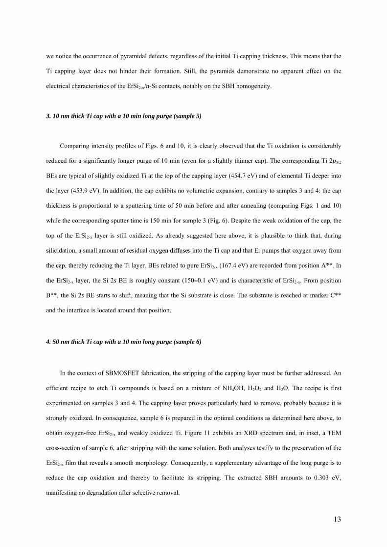
3. 10 nm thick Ti cap with a 10 min long purge (sample 5)
Comparing intensity profiles of Figs. 6 and 10, it is clearly observed that the Ti oxidation is considerably
reduced for a significantly longer purge of 10 min (even for a slightly thinner cap). The corresponding Ti 2p3/2
BEs are typical of slightly oxidized Ti at the top of the capping layer (454.7 eV) and of elemental Ti deeper into
the layer (453.9 eV). In addition, the cap exhibits no volumetric expansion, contrary to samples 3 and 4: the cap
thickness is proportional to a sputtering time of 50 min before and after annealing (comparing Figs. 1 and 10)
while the corresponding sputter time is 150 min for sample 3 (Fig. 6). Despite the weak oxidation of the cap, the
top of the ErSi2-x layer is still oxidized. As already suggested here above, it is plausible to think that, during
silicidation, a small amount of residual oxygen diffuses into the Ti cap and that Er pumps that oxygen away from
the cap, thereby reducing the Ti layer. BEs related to pure ErSi2-x (167.4 eV) are recorded from position A**. In
the ErSi2-x layer, the Si 2s BE is roughly constant (150±0.1 eV) and is characteristic of ErSi2-x. From position
B**, the Si 2s BE starts to shift, meaning that the Si substrate is close. The substrate is reached at marker C**
and the interface is located around that position.
4. 50 nm thick Ti cap with a 10 min long purge (sample 6)
In the context of SBMOSFET fabrication, the stripping of the capping layer must be further addressed. An
efficient recipe to etch Ti compounds is based on a mixture of NH4OH, H2O2 and H2O. The recipe is first
experimented on samples 3 and 4. The capping layer proves particularly hard to remove, probably because it is
strongly oxidized. In consequence, sample 6 is prepared in the optimal conditions as determined here above, to
obtain oxygen-free ErSi2-x and weakly oxidized Ti. Figure 11 exhibits an XRD spectrum and, in inset, a TEM
cross-section of sample 6, after stripping with the same solution. Both analyses testify to the preservation of the
ErSi2-x film that reveals a smooth morphology. Consequently, a supplementary advantage of the long purge is to
reduce the cap oxidation and thereby to facilitate its stripping. The extracted SBH amounts to 0.303 eV,
manifesting no degradation after selective removal.
13

Conclusions
In the present work, the chemical state of various Ti/Er/Si(100) stacks subjected to different RTA
conditions is examined in detail by means of XPS, with a peculiar focus on the chemical changes of Er. The
influence of the annealing temperature, the Ti cap thickness and the pre-annealing purge duration is investigated.
In the case of the as-deposited stack, the Er film is found to be oxygen-free, except for some superficial
oxidation. A shift of the Si spectra close to the interface with Si is disclosed, suggesting the onset of silicidation.
At 300 °C, the Er film is nearly completely oxidized, except in the vicinity of the interface where silicidation
appears predominant. For both cases, the formation of amorphous Er silicide is confirmed by HRTEM. At 600
°C, the formation of ErSi2-x is clearly identified by XRD and HRTEM. A significant part of the ErSi2-x film is
revealed to contain oxidized Er if the pre-annealing purge is too short. However, in the surroundings of the
interface to Si, XPS shows that ErSi2-x seems preserved, as also testified by a low SBH of 0.3 eV. An
improvement is observed for a long purge but the top of the ErSi2-x layer is still contaminated. Finally, provided
a thicker 50 nm Ti film covers the Er layer, an oxygen-free ErSi2-x film is grown and the cap stripping facilitated
if the pre-RTA purge is long.
From all the previous results, we can summarize that the Ti cap provides sufficient protection to allow for
silicidation, which always appears predominant over oxidation near the Si interface, regardless of the annealing
conditions.
Acknowledgements
This work was supported by the European Commission through the NANOSIL network of excellence
(FP7-IST-NoE-216171) and the METAMOS project (FP6-IST-STREP-016677).
14

1. I. Kim, S. K. Han, and C. M. Osburn, J. Electrochem. Soc., 151, F29 (2004). 2. W. He, S. Schuetz, R. Solanki, J. Belot, and J. McAndrew, Electrochem. Solid-State Lett., 7, G131 (2004). 3. T.-M. Pan, C.-S. Lai, H.-H. Hsu, C.-L. Chen, J.-D. Lee, K.-T. Wang, and J.-C. Wang, Appl. Phys. Lett., 87, 262908 (2005). 4. T.-M. Pan,_C.-L. Chen, W. W. Yeh, and S.-J. Hou, Appl. Phys. Lett., 89, 222912 (2006). 5. C.-J. Choi, M.-G. Jang, Y.-Y. Kim, M.-S. Jun, T.-Y. Kim, and M.-H. Song, Appl. Phys. Lett., 91, 012903 (2006). 6. J. Y. Duboz, P. A. Badoz, F. Arnaud d’Avitaya, and J. A. Chroboczek, Appl. Phys. Lett., 55, 84 (1989). 7. M. H. Unewisse and J. W. V. Storey, J. Appl. Phys., 73, 3873 (1993). 8. N. Reckinger, X. Tang, V. Bayot, D. A. Yarekha, E. Dubois, S. Godey, X. Wallart, G. Larrieu, A. Łaszcz, J. Ratajczak, P. J. Jacques, and J.-P. Raskin, J. Appl. Phys., 104, 103523 (2008). 9. M. Yang, Y. Kim, J. Shin, S. Lee, and K. Park, Appl. Phys. Lett., 84, 741 (2004). 10. E. J. Tan, K.-L. Pey, N. Singh, G.-Q. Lo, D. Z. Chi, Y. K. Chin, K. M. Hoe, G. Cui, and P. S. Lee, IEEE Electron Device Lett., 29, 1167 (2008). 11. G. Larrieu, D. A. Yarekha, E. Dubois, N. Breil, and O. Faynot, IEEE Electron Device Lett., 30, 1266 (2009). 12. L. Pahun, Y. Campidelli, F. Arnaud d’Avitaya, and P. A. Badoz, Appl. Phys. Lett., 60, 1166 (1992). 13. J. E. Baglin, F. M. d’Heurle, and C. S. Petersson, Appl. Phys. Lett., 36, 594 (1980). 14. P. Muret, T. A. Nguyen Tan, N. Frangis, and J. Van Landuyt, Phys. Rev. B, 56, 9286 (1997). 15. J. Y. Veuillen, T. A. Nguyen Tan, D. B. B. Lollman, N. Guerfi, and R. Cinti, Surf. Sci., 251/252, 432 (1991). 16. P. Wetzel, L. Haderbache, C. Pirri, J. C. Peruchetti, D. Bolmont, and G. Gewinner, Surf. Sci., 251/252, 799 (1991). 17. X. Tang, J. Katcki, E. Dubois, N. Reckinger, J. Ratajczak, G. Larrieu, P. Loumaye, O. Nisole, and V. Bayot, Solid-State Electron., 47, 2105 (2003). 18. Y.-L. Jiang, Q. Xie, C. Detavernier, R. L. Van Meirhaeghe, G.-P. Ru, X.-P. Qu, B.-Z. Li, A. Huang, and P. K. Chu, J. Vac. Sci. Technol. A, 25, 285 (2007). 19. W. Huang, G. P. Ru, Y. L. Jiang, X. P. Qu, B. Z. Li, and R. Liu, Thin Solid Films, 516, 4252 (2008). 20. D. B. B. Lollman, T. A. Nguyen Tan, and J.-Y. Veuillen, Surf. Sci., 269/270, 959 (1992). 21. S. Gokhale, S. Mahamuni, S. V. Deshmukh, V. J. Rao, A. S. Nigavekar, and S. K. Kulkarni, Surf. Sci., 237, 127 (1990). 22. P. Wetzel, L. Haderbache, C. Pirri, J. C. Peruchetti, D. Bolmont, and G. Gewinner, Phys. Rev. B, 43, 6620 (1991). 23. N. Guerfi, T. A. Nguyen Tan, J. Y. Veuillen, and D. B. Lollman, Appl. Surf. Sci., 56/58, 501 (1992). 24. S. Kennou, S. Ladas, M. G. Grimaldi, T. A. Nguyen Tan, and J. Y. Veuillen, Appl. Surf. Sci., 102, 142 (1996). 25. F. P. Netzer, R. A. Wille, and M. Grunze, Surf. Sci., 102, 75 (1981). 26. Y. Uwamino, T. Ishizuka, and H. Yamatera, J. Electron Spectrosc. Relat. Phenom., 34, 67 (1984). 27. G. T. K. Swami, F. E. Stageberg, and A. M. Goldman, J. Vac. Sci. Technol. A, 2, 767 (1984). 28. N. Reckinger, X. Tang, V. Bayot, D. A. Yarekha, E. Dubois, S. Godey, X. Wallart, G. Larrieu, A. Łaszcz, J. Ratajczak, P. J. Jacques, and J.-P. Raskin, Appl. Phys. Lett., 94, 191913 (2009). 29. C. D. Wagner, W. M. Riggs, L. E. Davis, and J. F. Moulder, in Handbook of X-Ray Photoelectron Spectroscopy, 1st ed., G. E. Muilenberg, Editor, Perkin-Elmer Corporation, Eden Prairie (1979). 30. K. Hafidi, Y. Ijdiyaou, M. Azizan, E. L. Ameziane, A. Outzourhit, T. A. Nguyen Tan, and M. Brunel, Appl. Surf. Sci., 108, 251 (1997). 31. G. Larrieu, E. Dubois, X. Wallart, X. Baie, and J. Katcki, J. Appl. Phys., 94, 7801 (2003). 32. V. V. Atuchin, V. G. Kesler, N. V. Pervukhina, and Z. Zhang, J. Electron Spectrosc. Relat. Phemon., 152, 18 (2006). 33. B. Demri, M. Hage-Ali, M. Moritz, J. L. Kahn, and D. Muster, Appl. Surf. Sci., 108, 245 (1997).
15
34. P. R. Moses, L. M. Wier, J. C. Lennox, H. O. Finklea, J. R. Lenhard, R. W. Murray, Anal. Chem., 50, 576 (1978). 35. T. Ogama, J. Appl. Phys., 64, 753 (1988). 36. M. Anpo, H. Nakaya, S. Kodama, Y. Kubokawa, K. Domen, and T. Onishi, J. Phys. Chem., 90, 1633 (1986). 37. S. Badrinarayanan, S. Sinha, and A. B. Mandale, J. Electron Spectrosc. Relat. Phemon., 49, 303 (1989). 38. D. Gonbeau, C. Guimon, G. Pfister-Guillouzo, A. Levasseur, G. Meunier, and R. Dormoy, Surf. Sci., 254, 81 (1991). 39. W. Huang, G. P. Ru, Y. L. Jiang, X. P. Qu, B. Z. Li, R. Liu, and F. Lu, J. Vac. Sci. Technol. B, 26, 164 (2008). 40. L. J. Chen, Mater. Sci. Eng. R., 29, 115 (2000). 41. G. J. Campisi, A. J. Bevolo, and F. A. Schmidt, J. Appl. Phys., 52, 6647 (1981). 42. CRC Handbook of Chemistry and Physics, 79th ed., D. R. Lide, Editor, CRC Press, Boca Raton (1998). 43. J. E. E. Baglin, F. M. d'Heurle, and C. S. Petersson, J. Appl. Phys., 52, 2841 (1981). 44. E. Dubois and G. Larrieu, J. Appl. Phys., 96, 729 (2004). 45. E. J. Tan, M. Bouville, D. Z. Chi, K. L. Pey, P. S. Lee, D. J. Srolovitz, and C. H. Tung, Appl. Phys. Lett., 88, 021908 (2006).
16

Figure 1. (Color online) XPS intensity depth profile of the as-deposited Ti(10 nm)/Er(25 nm)/Si(100) stack.
Particular positions along the profile are marked by labels A to G. Inset: Cross-sectional HRTEM picture of the
interface between a-Er/Si and Si.
Figure 2. (Color online) Typical normalized Er 4d core level spectra after background subtraction for metallic
and oxidized Er, respectively. The spectra are obtained from a thick Er layer to serve as a reference. The Er 4d5/2
main peak of elemental Er is located at 167.1 eV while its satellite is at 169.2 eV. Oxidized Er is characterized
by a unique peak at 169.3 eV.
17

Figure 3. (Color online) (a) Er 4d5/2 and Si 2p BEs for the as-deposited Ti(10 nm)/Er(25 nm)/Si(100) stack, from
marker C. (b) Normalized Er 4d core level spectra after background subtraction for the same stack, for markers
C to F.
Figure 4. (Color online) XPS intensity depth profile of the Ti(10 nm)/Er(25 nm)/Si(100) stack annealed at 300
°C for 2 min with a 2 min pre-RTA purge. Particular positions along the profile are marked by labels A’ to I’.
Inset: Cross-sectional HRTEM picture of the interface between a-Er/Si and Si.
18

Figure 5. (Color online) (a) Er 4d5/2 and Si 2s BEs for the Ti(10 nm)/Er(25 nm)/Si(100) stack annealed at 300 °C
for 2 min with a 2 min pre-RTA purge, from marker D’. (b) Normalized Er 4d core level spectra after
background subtraction for the same stack, for markers C’ to G’.
Figure 6. (Color online) XPS intensity depth profile of the Ti(15 nm)/Er(25 nm)/Si(100) stack annealed at 600
°C for 2 min with a 2 min pre-RTA purge. Particular positions along the profile are marked by labels A’’ to F’’.
Inset 1: Cross-sectional HRTEM picture of the interface between ErSi2-x and Si. Inset 2: XRD spectrum with a
strong peak corresponding to ErSi2-x.
19

Figure 7. (Color online) Normalized (a) Si 2p and (b) Er 4d core level spectra after background subtraction for
the Ti(15 nm)/Er(25 nm)/Si(100) stack annealed at 600 °C for 2 min with a 2 min pre-RTA purge. (c) Er 4d5/2
and Si 2p BEs for the same stack, from marker B’’.
20

Figure 8. (Color online) Experimental (markers) and modeled (solid lines) Arrhenius plots for the Ti(15
nm)/Er(25 nm)/Si(100) stack annealed at 600 °C for 2 min with a 2 min pre-RTA purge (blue) and for the Ti(50
nm)/Er(25 nm)/Si(100) stack annealed at 600 °C for 2 min with a 2 min pre-RTA purge (red). The current-
voltage measurements are performed between 150 and 290 K with a step of 20 K, for biases ranging from 0.1 V
up to 1 V with a step of 0.15 V. The average error on the extracted SBH lies within 5 meV. Insets: Typical
experimental current-voltage characteristics at 150 and 290 K.
21

Figure 9. (Color online) (a) XPS intensity depth profile of the Ti(50 nm)/Er(25 nm)/Si(100) stack annealed at
600 °C for 2 min with a 2 min pre-RTA purge. Particular positions along the profile are marked by labels A* to
E*. TEM micrographs of the same stack (b) left as-deposited and (c) after annealing.
22

Figure 10. (Color online) XPS intensity depth profile of the Ti(10 nm)/Er(25 nm)/Si(100) stack annealed at 600
°C for 2 min with a 10 min pre-RTA purge. Particular positions along the profile are marked by labels A** to
C**.
Figure 11. (Color online) XRD spectrum of the Ti(50 nm)/Er(25 nm)/Si(100) stack annealed at 600 °C for 2 min
with a 10 min pre-RTA purge. Inset: Corresponding cross-sectional TEM picture.
23

Table I: Summary of the stack composition and RTA conditions for allconsidered samples.
Sample Ti thickness [nm] Annealing temperature [°C]
Pre-RTA purge duration [min]
1 (10/no/2) 10 no 2 2 (10/300/2) 10 300 2 3 (15/600/2) 15 600 2 4 (50/600/2) 50 600 2 5 (10/600/10) 10 600 10 6 (50/600/10) 50 600 10
24

Table II: XPS BEs relevant to Er 4d5/2, O 1s, Si 2p/2s, and Ti 2p3/2 core levels stemming from the literature and determined in this work.
Peak Compound BE [eV] Reference 167.4+169 (sat.) Swami
167.6 Kennou 167.1 Reckinger Er
167.1 This work 167.6 Kennou ErSi2-x 167.3 This work 167.3 Reckinger a-Er/Si 167.3 This work 168.7 Uwamino 168.6 Swami 168.8 Wagner Er2O3
170.4 Guerfi , Kennou 169.2 Kennou 169.5 Reckinger ErOx
169.1-169.5 This work 170 Hafidi
Er 4d5/2
ErSixOy 169-169.7 Choi 530.6 Swami Er2O3 531.6 Guerfi , Netzer
ErOx 531 This work SiOx (x ≈ 1) 532-533 Kennou
533.2 Kennou SiO2 533.1 Larrieu 529.3-531 Atuchin
530.5 Demri TiO2
529.8 Moses
O 1s
ErSixOy 531.1 Pan 150.7 Ogama
150.5-150.6 Reckinger Si 150.5 This work
SiO2 154.2 Anpo ErSi2-x 150.1 This work
149.5 Reckinger
Si 2s
a-Er/Si 149.6 This work 99.3 Lollman , Gokhale Si 99.1 This work 99 Lollman ErSi2-x 98.7 This work
98.1 Lollman Shift: 0 to 1.3 Wetzel a-Er/Si Si 2p
98.3 This work ~103 Guerfi SiO2 ~103.3 Hafidi ~102 Guerfi SiOx
ErSixOy ~103.8 Hafidi 454 Atuchin Ti 454 Badrinarayanan
Ti 2p3/2 459 Atuchin TiO2 458.9 Gonbeau
458.9 Demri
25

Table III: Summary of the Ti 2p3/2, O 1s, Er 4d5/2, and Si 2p/2s BEs [eV] recorded at the different markers and corresponding composition, for samples 1 to 5.
Sample Marker Sputter time [min]
Ti 2p3/2 O 1s Er 4d5/2 Si 2p/2s Composition
A 0 458.9 530.5 X X TiO2
B 56 453.7 530.9 167.7 X Ti + Er C 68 453.7 530.7 167.1 X ErOx
1 (10/no/2) D 80 453.5 530.7 167.1 X Er E 112 X X 167.1 98.3 a-Er/Si F 132 X X 167.3 98.9 a-Er/Si G 156 X X 167.3 99.1 Si A’ 0 459 530.5 X X TiO2
B’ 56 454 530.9 169.4 X Ti + ErOx
C’ 96 454 531.1 169.5 X ErOx
D’ 124 X 531.1 169.5 149.5 Er-Si-O 2 (10/300/2) E’ 152 X 531.1 169.1 149.7 Er-Si-O
F’ 168 X 531 167.5 149.6 Er-Si-O G’ 184 X 530.7 167.3 149.8 a-Er-Si
H’ 208 X X 167.3 150.3 a-Er-Si I’ 236 X X 167.5 150.5 Si
A’’ 0 459.1 530.5 X X TiO2
B’’ 152 455.1 531.1 169.1 102.9/98.8 Er-Si-O C’’ 200 454.1 531 169.1 98.9 Er-Si-O 3 (15/600/2) D’’ 248 X 530.9 167.5 98.6 Er-Si-O E’’ 276 X 530.3 167.3 98.7 ErSi2-x
F’’ 300 X X 167.3 99.1 Si A* 48 454 531.4 X 149.7 TiOx
B* 96 453.8 531.2 X 149.8 Ti 4 (50/600/2) C* 152 453.8 530.9 167.3 149.9 Ti + ErSi2-x
D* 232 X X 167.3 150 ErSi2-x
E* 280 X X 167.3 150.5 Si A** 148 X 531.1 167.5 150.1 Er-Si-O B** 204 X X 167.3 150.2 ErSi2-x5 (10/600/10) C** 220 X X 167.3 150.5 Si
26