Single step fabrication of N-doped graphene/Si3N4/SiC heterostructures
9
Single step fabrication of N-doped graphene/Si 3 N 4 /SiC heterostructures Emilio Vélez-Fort 1,2 , Emiliano Pallecchi 1 , Mathieu G. Silly 3 , Mounib Bahri 1 , Gilles Patriarche 1 , Abhay Shukla 2 , Fausto Sirotti 3 , and Abdelkarim Ouerghi 1 ( ) 1 CNRS-Laboratoire de Photonique et de Nanostructures (LPN), Route de Nozay, Marcoussis 91460, France 2 Université Pierre et Marie Curie (CNRS – IMPMC), 4 Pl. Jussieu, Paris 75005, France 3 Synchrotron-SOLEIL, Saint-Aubin, BP48, F91192 Gif sur Yvette Cedex, France Received: 24 November 2013 Revised: 28 January 2014 Accepted: 1 March 2014 © Tsinghua University Press and Springer-Verlag Berlin Heidelberg 2014 KEYWORDS epitaxial graphene, spectroscopy, nitrogen-doped graphene, low-energy electron microscopy, electronic properties ABSTRACT In-plane heteroatom substitution of graphene is a promising strategy to modify its properties. The ability to dope graphene with electron-donor nitrogen heteroatoms is highly important for modulating electrical properties of graphene. Here we demonstrate a transfer-free method to directly grow large area quasi free-standing N-doped graphene bilayers on an insulating substrate (Si 3 N 4 ). Electron-bombardment heating under nitrogen flux results in simultaneous growth of N-doped graphene and a Si 3 N 4 layer on the SiC surface. The decoupling of N-doped graphene from the substrate and the presence of Si 3 N 4 are identified by X-ray photoemission spectroscopy and low-energy electron diffraction. The substitution of nitrogen atoms in the graphene planes was confirmed using high resolution X-ray photoemission spectroscopy which reveals several atomic configurations for the nitrogen atoms: Graphitic-like, pyridine-like, and pyrrolic- like. Furthermore, we demonstrated for the first time that N-doped graphene could be used to efficiently probe oxygen molecules via nitrogen atom defects. 1 Introduction Graphene is a novel two-dimensional material with great potential for applications in nanoelectronics, mainly due to its extremely high electron mobility, which is a consequence of the high Fermi velocity and the linear dispersion relation around the Dirac point [1–3]. It is ambipolar and exhibits ballistic transport on a micrometer scale up to room temperature. In addition, graphene is also interesting for spintronic devices, such as spin qubits and spin diodes, because of its long spin-coherence time and long spin relaxation time [4–6]. One of the most promising techniques to synthesize graphene for electronic devices is the epitaxial growth on silicon carbide (SiC). The epitaxial growth of graphene offers the possibility to produce wafer scale graphene domains and is compatible with silicon technology [7, 8]. The idea behind this method is to sublime the Si contained in the SiC by increasing gradually the temperature of the SiC substrate. At sufficiently high temperature, the remaining carbon Nano Research DOI 10.1007/s12274-014-0444-9 Address correspondence to abdelkarim. [email protected]
-
Upload
independent -
Category
Documents
-
view
0 -
download
0
Transcript of Single step fabrication of N-doped graphene/Si3N4/SiC heterostructures

Single step fabrication of N-doped graphene/Si3N4/SiC heterostructures
Emilio Vélez-Fort1,2, Emiliano Pallecchi1, Mathieu G. Silly3, Mounib Bahri1, Gilles Patriarche1, Abhay Shukla2,
Fausto Sirotti3, and Abdelkarim Ouerghi1 ()
1 CNRS-Laboratoire de Photonique et de Nanostructures (LPN), Route de Nozay, Marcoussis 91460, France 2 Université Pierre et Marie Curie (CNRS – IMPMC), 4 Pl. Jussieu, Paris 75005, France 3 Synchrotron-SOLEIL, Saint-Aubin, BP48, F91192 Gif sur Yvette Cedex, France
Received: 24 November 2013
Revised: 28 January 2014
Accepted: 1 March 2014
© Tsinghua University Press
and Springer-Verlag Berlin
Heidelberg 2014
KEYWORDS
epitaxial graphene,
spectroscopy,
nitrogen-doped graphene,
low-energy electron
microscopy,
electronic properties
ABSTRACT
In-plane heteroatom substitution of graphene is a promising strategy to modify
its properties. The ability to dope graphene with electron-donor nitrogen
heteroatoms is highly important for modulating electrical properties of graphene.
Here we demonstrate a transfer-free method to directly grow large area quasi
free-standing N-doped graphene bilayers on an insulating substrate (Si3N4).
Electron-bombardment heating under nitrogen flux results in simultaneous
growth of N-doped graphene and a Si3N4 layer on the SiC surface. The decoupling
of N-doped graphene from the substrate and the presence of Si3N4 are identified
by X-ray photoemission spectroscopy and low-energy electron diffraction. The
substitution of nitrogen atoms in the graphene planes was confirmed using
high resolution X-ray photoemission spectroscopy which reveals several atomic
configurations for the nitrogen atoms: Graphitic-like, pyridine-like, and pyrrolic-
like. Furthermore, we demonstrated for the first time that N-doped graphene
could be used to efficiently probe oxygen molecules via nitrogen atom defects.
1 Introduction
Graphene is a novel two-dimensional material with
great potential for applications in nanoelectronics,
mainly due to its extremely high electron mobility,
which is a consequence of the high Fermi velocity and
the linear dispersion relation around the Dirac point
[1–3]. It is ambipolar and exhibits ballistic transport
on a micrometer scale up to room temperature. In
addition, graphene is also interesting for spintronic
devices, such as spin qubits and spin diodes, because
of its long spin-coherence time and long spin relaxation
time [4–6].
One of the most promising techniques to synthesize
graphene for electronic devices is the epitaxial growth
on silicon carbide (SiC). The epitaxial growth of
graphene offers the possibility to produce wafer scale
graphene domains and is compatible with silicon
technology [7, 8]. The idea behind this method is to
sublime the Si contained in the SiC by increasing
gradually the temperature of the SiC substrate. At
sufficiently high temperature, the remaining carbon
Nano Research
DOI 10.1007/s12274-014-0444-9
Address correspondence to abdelkarim. [email protected]
| www.editorialmanager.com/nare/default.asp
2 Nano Res.
atoms rearrange and form a graphitic honeycomb
lattice on top of the SiC. On the Si face of a silicon
carbide wafer, the first carbon layer is strongly bound
to the substrate which drastically changes its electronic
proprieties. This layer, also referred to as the interface
or buffer layer, displays a large band gap and is
therefore insulating despite its honeycomb lattice
configuration. However, the next graphitic layer
which is grown on top of the interface layer shows the
well-known electronic proprieties of graphene, namely
a zero bandgap and the linear dispersion around the
K and K' points. Moreover, the presence of Si dangling
bonds underneath the buffer layer degrades the charge
carrier mobility due to the high intrinsic doping [9].
To succeed in developing high performance graphene-
based electronic devices, we must be able to dispense
with the interface layer without losing the exceptional
intrinsic carrier mobility of graphene [10–14]. Further,
doped graphene structures have attracted considerable
interest among the scientific community [15–20]. Like
other doped carbon forms, N-doped graphene is
expected, for example, to have enhanced properties for
Li-battery applications [21]. Reports of the synthesis of
N-doped graphene are scarce and the development of a
simple method to synthesize N-doped graphene is
needed. Nitrogen doping can enhance the conduc-
tivity of graphene and induce n-type semiconductor
behavior [22]. More importantly, incorporating nitrogen
atoms in different bonding configurations into the
carbon network would provide the N-doped graphene
with more functional groups for property design.
Ammonia-assisted doping methods have been reported
for graphene grown with different techniques such
as chemical vapor deposition, arc discharge of carbon
electrodes and thermal annealing of graphene oxide
[23–25].
Recent discoveries demonstrate that a widely
tunable bandgap can be realized in bilayer graphene
and bilayer graphene–boron nitride heterostructures
(h-BN), which opens a new door for applications of
graphene in electronic and optical devices [26, 27].
Here, we demonstrate an approach to grow quasi
free-standing N-doped graphene on a Si3N4 insulating
substrate. This result is obtained by exposing the
substrate to nitrogen gas during the graphene growth.
This method offers a number of advantages: (i) It is a
single step process; (ii) the tuning of the nitrogen flux
intensity can induce quasi free-standing growth; (iii)
the graphene is doped in situ, during the growth.
More precisely, we report on the formation of N-doped
bilayer graphene on SiC and its electronic properties.
The graphene layers were investigated by low-energy
electron diffraction (LEED), atomic force microscopy
(AFM), X-ray photoelectron spectroscopy (XPS), Raman
scattering and transmission electron microscopy
(TEM). The XPS spectra show three types of nitrogen
doping sites: Graphitic, pyridinic and pyrrolic nitrogen.
Decoupling of the buffer layer from the substrate
and the associated physical and electronic structural
changes are observed via LEED. The LEED and XPS
results demonstrate that a decoupled graphene bilayer
is formed on top of the SiC substrate. Moreover, we
show that a Si3N4 interfacial layer is formed by dilute
nitrogen situated between the graphene and SiC
substrate.
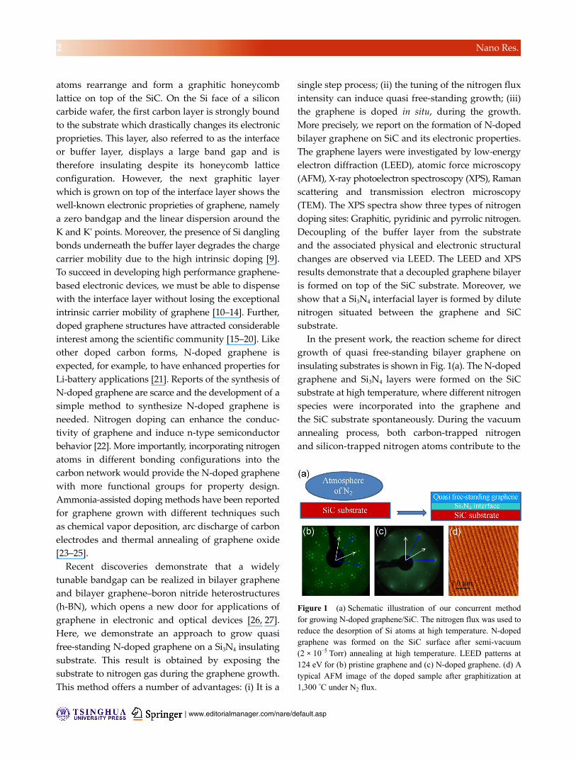
In the present work, the reaction scheme for direct
growth of quasi free-standing bilayer graphene on
insulating substrates is shown in Fig. 1(a). The N-doped
graphene and Si3N4 layers were formed on the SiC
substrate at high temperature, where different nitrogen
species were incorporated into the graphene and
the SiC substrate spontaneously. During the vacuum
annealing process, both carbon-trapped nitrogen
and silicon-trapped nitrogen atoms contribute to the
Figure 1 (a) Schematic illustration of our concurrent method for growing N-doped graphene/SiC. The nitrogen flux was used to reduce the desorption of Si atoms at high temperature. N-doped graphene was formed on the SiC surface after semi-vacuum (2 × 10⁻⁵ Torr) annealing at high temperature. LEED patterns at 124 eV for (b) pristine graphene and (c) N-doped graphene. (d) A typical AFM image of the doped sample after graphitization at 1,300 °C under N2 flux.

www.theNanoResearch.com∣www.Springer.com/journal/12274 | Nano Research
3 Nano Res.
nitridation of the SiC surface and convert the epitaxial
graphene into N-doped graphene. Pristine graphene
(PG) was synthesized similarly by annealing a SiC
substrate under argon atmosphere. After growth, N-
doped graphene (NG) and pristine graphene (PG) can
be transferred ex situ for further characterization.
2 Methods
Graphene samples were grown on a n-type Si ter-
minated 6H-SiC(0001) wafer. The substrate was first
etched in a hydrogen flux at 1,500 °C at 200 mbar
for 15 min in order to clean the surface and form a
step-ordered structure. After etching, the substrate was
transferred into an ultrahigh vacuum (UHV) chamber
with a base pressure of 1 × 10⁻⁹ Torr. The surface of
the substrate was first degassed for several hours at
600 °C to eliminate all the impurities and then annealed
under a Si flux (2 monolayers per minute (ML/min)) at
900 °C to remove the native oxide. The graphitization
process was performed under a nitrogen flux and the
base pressure of the system was maintained around
2 × 10⁻⁵–2 × 10⁻⁴ Torr. The growth was performed by
annealing the surface with an electron bombardment
technique. The sample was heated gradually from
800 °C to 1,300 °C. After the growth of the graphene
layer, the sample was quenched to 500 °C under
nitrogen flux (1 ML/min) [28]. In order to compare our
results, pristine graphene was also synthesized with a
similar method but using an argon flux instead of the
nitrogen flux. The chemical, electronic and structural
properties of the resulting films were investigated
by means of XPS, LEED, AFM, TEM and Raman
spectroscopy. The micro Raman spectroscopy was
performed at room temperature with a Renishaw
spectrometer using 532 nm laser light focused on the
sample by a DMLM Leica microscope with a 100 ×
(NA = 0.75) objective and a power of 5 mW with a spot
size of about 1 μm. High-resolution core level X-ray
synchrotron radiation experiments were carried out at
the third generation SOLEIL storage ring (Saint-Aubin,
France) operated in the top-up mode at 430 mA, using
the photoemission end station of the TEMPO beamline
which covers a photon energy range of 50–1500 eV.
The experiments were performed at room temperature
with a base pressure of 2 × 10⁻¹⁰ mbar. Photoelectrons
were analyzed at a take-off angle of 90° with respect
to the sample surface using a Scienta SES 2002 hemi-
spherical analyzer and a delay-line detector [29].
3 Results and discussion
First, we characterized the graphene crystallographic
structure by low-energy electron diffraction. Figure 1(b)
shows the LEED image of pristine graphene. A single
phase of graphene layer is formed as deduced from
the very well ordered (6 3 6 3) R30° LEED pattern
that corresponds to a carbon-rich termination. The
smallest hexagons around the integer spots are due
to double diffraction as a result of a (6 3 6 3) R30°
reconstruction of the interfacial layer. These LEED
findings match previously reported results [8, 30].
Figure 1(c) shows the typical LEED pattern of the
doped sample after graphitization at 1,300 °C under
N2 flux. Two contributions can be clearly distinguished
in the LEED diagram. The first one arising from the
(1 × 1) graphene layer confirms the presence of this
material at the surface of the sample (blue arrows).
The second one, which is characterized by isotropic
(1 × 1) spots, is the 6H-SiC substrate (white arrows).
This finding indicates the presence of oriented single-
domain graphene patches forming a layer, and the
absence of rotational disorder and twinning domains.
Importantly, the absence of the six satellites spots in
the pattern of N-doped graphene clearly demonstrates
that the (6 3 6 3) R30° reconstruction is not present
in our sample. This structure is well known and
refers to the buffer layer (interface layer) [31]. This
result indicates that the buffer layer is not present for
epitaxial graphene grown under N2 flux in our growth
conditions. A careful analysis of the XPS (discussed
below) shows that N-doped graphene is a bilayer
while PG a monolayer. In order to assess the mor-
phology of the graphene layer, AFM was performed in
tapping mode. Figure 1(d) shows typical AFM image
of the sample. It is clearly observed that the terraces
on the SiC surface are atomically flat and separated
by straight step edges. The average terrace width is
600 nm. We also see white spots which are possibly
due to physisorbed nitrogen on the surface. We then

| www.editorialmanager.com/nare/default.asp
4 Nano Res.
measured the Raman spectra on the same sample at
room temperature shown in Fig. 2(a). The measure-
ments were performed for the N-doped bilayer
graphene (NG, red curve) on 6H-SiC(0001) and for the
pristine graphene (PG, black curve). The graphene
layer has several overtone peaks in the 1,000–2,000 cm–1
regime. The peak at 1,522 cm–1 is considered to be an
overtone of the L-point optical phonon from the
SiC. The Raman signals from the graphene show
prominent characteristic peaks at 1,620 cm–1 (G) and
2,732 cm–1 (2D), which give evidence of carbon sp2
reorganization [32]. The G peak value of 1,620 cm–1
could indicate strong N-doping. Also the blue-shifted
position of the 2D peak at 2,732 cm–1 indicates
compressive strain of the graphene layer during the
post-growth cooling down procedure or charge
transfer doping from the substrate. The blue shift of
the G and 2D band has also been reported in epitaxial
graphene on 6H-SiC wafers [33]. The 2D peak is
however much broader than in isolated graphene
with a full width at half maximum (FWHM) of around
70 cm–1. The broadening can be attributed both to
defect scattering and two- or more layer graphene
formation. The strong intensity of the D peak (in
comparison to the G peak) is a clear indication of
zone-boundary phonons scattering on defects, not
allowed in ideal graphene due to the large wave-
vector of the K-point phonon involved. Its presence is
an indication of disorder, such as finite size domains.
The D bands of N-doped graphene can be significantly
high with respect to PG because formation of pyridinic
and pyrrolic nitrogen sites is accompanied by defects
inside the graphene network and functional edges of
the graphene layer. The ratio of the integrated inten-
sities of D to G bands (ID/IG) can be used to estimate
the crystallite size (La) of graphene. We calculated La
of graphene by the following equation [34],
1
10 4 Da laser
G
nm 2, 4.10I
LI
where λlaser is the Raman excitation wavelength (λlaser =
532 nm). The values of ID/IG for PG and N-doped gra-
phene are 0.14 and 0.6, which correspond to crystallite
sizes of 137 nm and 32 nm, respectively.
Cross-sectional TEM samples were prepared using
a focused ion beam (FIB). Protective layers of amor-
phous carbon were deposited on the sample, initially
with the electron beam to avoid surface damage.
Images were obtained in STEM mode using a Cs-probe
aberration corrected JEOL 2200 FS STEM. Figure 2(b)
shows a cross-sectional TEM image for the N-doped
graphene on SiC(0001). The high resolution image
in Fig. 2(b) shows that Si3N4 was grown epitaxially on
SiC(0001) at this temperature. The TEM diffraction pat-
tern indicates and confirms that (112—
0)Si3N4//(0001)SiC,
namely the c-axis of Si3N4, is parallel to the SiC(0001)
surface. The line profile in Fig. 2(b) of the SiC planes
confirms that their spacing is indeed constant (2.43 Å
and 2.66 Å) and attests to the abruptness of the
formation of the Si3N4 and SiC interface under the
growth conditions reported here. No detectable sign
Figure 2 (a) Micro-Raman spectra of the D, G and 2D bands, for the N-doped (red) and pristine (black) graphene. (b) High-resolution STEM image obtained of the sample annealed under N2 (inset STEM image showing the interface layer).

www.theNanoResearch.com∣www.Springer.com/journal/12274 | Nano Research
5 Nano Res.
of interdiffusion and intermixing has been observed.
We measured a distance of 4 Å between each graphene
layer; this value is very close to the bulk interplanar
distance (3.376 Å).
To investigate the elemental composition as well
as the chemical bonding environment of N atoms in
N-doped graphene, XPS measurements were carried
out for N-doped and pristine graphene, as shown in
Fig. 3. The experimental C 1s spectra and their fitting
curves are reported in Fig. 3(a) for the pristine and
N-doped graphene layers. Raw data for PG represented
by red disks are shown together with the results of
the curve fitting of the C 1s spectra on the top panel
(black curve). Given the asymmetrical shape of the
graphene component, three contributions have to be
considered to obtain consistent fits using a least-square
fitting procedure: The small component (IL) located
at 285.4 eV (FWHM = 1 eV), the stronger one (G) at
284.6 eV (FWHM = 0.53 eV), and the bulk component
(SiC) at 283.8 eV (FWHM = 0.95 eV). These three peaks
(IL, G and SiC) can be, respectively, ascribed to interface
layer, graphene layer and bulk contribution. No other
chemically shifted peak is needed to fit the spectrum.
Figure 3 (a) C 1s XPS spectra for epitaxial pristine graphene annealed at 1,350 °C at hν = 340 eV (top panel) and for N-doped graphene at hν = 340 eV (middle panel) and hν = 600 eV (bottom panel). The spectra were fitted using a Doniach–Sunjic line-shape analysis. (b) Si 2p XPS spectra for pristine and N-doped graphene at hν = 340 eV (surface sensitive) and hν = 600 eV (bulk sensitive). XPS measurements were performed at = 45° emerging angle with respect to the sample normal.
The XPS C 1s spectra for the N-doped graphene are
presented in Fig. 3(a) (middle and bottom panels).
Again, we found the two peaks at 283.2 eV (FWHM =
0.85 eV) and 284.6 eV (FWHM = 1.1 eV) which are
attributed to bulk Si–C bonds and C–C bonds
(graphene) and a new one at 286 eV (FWHM = 1.3 eV)
arising from the C–N bonds [35]. The main difference
for N-doped graphene compared to PG is the absence
of the interface layer peak at 285.4 eV. This observation,
which is consistent with our LEED results, confirms
the absence of a carbon-rich buffer layer. We notice an
important difference between the FWHM of graphene
peaks in PG and N-doped graphene: This can be
explained by a disorder induced on the graphene
layer due to the presence of nitrogen (seen as well in
the Si 2p core level spectrum). Also, the SiC bulk
component in the C 1s and Si 2p (Fig. 3) core level
spectra shifts 0.6 eV towards lower binding energy.
This reveals that the NG/SiC interfacial region is
modified for growth under N2 flux, because of a
different band bending [10]. It is worth noting the lack
of C–O components in the C 1s core-level spectrum.
This shows that the oxygen does not interact covalently
with the carbon layers in our material. The number
of layers present in each of our samples was also
deduced from our photoemission results. Assuming
homogenous two-dimensional graphene growth,
we can estimate the thickness of graphene using a
simple attenuation model. The estimated thickness
for our samples was 2 ML for the decoupled N-doped
graphene and monolayer for the PG.
In order to investigate the decoupling of the doped
graphene layer and the SiC substrate, we turn now to
the investigation of the interfacial region. Here the
Si 2p XPS spectra allow information about the com-
position of this region to be extracted. Figure 3(b)
shows the Si 2p spectra for N-doped (middle and
bottom panels) and pristine epitaxial graphene (top
panel). Both spectra consist of a dominant Si 2p
spin–orbit split doublet at 101.5 eV for PG and 100.9 eV
for N-doped graphene. The small shoulder at 102.1 eV
in pristine graphene is attributed to the interface
layer area of the SiC(0001) substrate. For the N-doped
graphene spectrum, we found additional Si 2p
components at higher binding energies: At 101.3 eV,
101.6 eV and 103.1 eV, due to Si–N–C units, Si3N4 and

| www.editorialmanager.com/nare/default.asp
6 Nano Res.
Si–O bonds respectively. The peak located at 101.6 eV
is a first important signature of silicon nitride for-
mation [36]. At lower photon energy (340 eV, middle
panel) where the surface sensitivity is higher, this
signal from Si3N4 is strong, whereas it becomes weaker
at higher photon energy or less surface-sensitive con-
ditions (600 eV, bottom panel). This implies that the
graphene/SiC interfacial region can also be modified
under a N2 flux and results in silicon nitride formation
between the N-doped graphene layer and the SiC
substrate.
Based on the peak area ratio of the silicon nitride
component and the SiC component in the fitted Si 2p
spectra, we can estimate the thicknesses of the silicon
nitride passivation layers in our sample to be about
1.0 nm. The passivation of SiC suggests that higher
substrate temperature under N2 flux leads to a higher
nitridation rate when other variables (nitrogen partial
pressure and time of graphitization) are kept the
same. These values are close to the N 1s binding energy
of hexagonal silicon nitride (h-Si3N4). Furthermore,
the ratio of peak area for these N 1s component peaks
to the Si 2p component peaks at 101.6 eV were cal-
culated to be around 1.3 confirming that Si3N4 is the
main product in the passivation layer on the SiC
surface. Figure 4(a) shows the decomposition of the
N 1s spectrum for the nitrogen sample. The N 1s peak
can be resolved into five components centered at
397.7 eV (N1), 398.9 eV (N3), 398 eV (N2), 400.9 eV
(N4), and 401.4 eV (N5) representing Si–N, N–O,
pyridinic, pyrrolic, and graphitic type of N atoms
present in the sample, respectively. The differences
between N2, N4 and N5 are shown schematically in
Fig. 4(b), a top view of a graphene layer with nitrogen
defects. The graphitic-like configuration corresponds
to a direct substitution of a carbon atom by a nitrogen
atom, while the pyridinic and pyrrolic structures
correspond to a nitrogen atom bonded to two carbon
atoms in a six-atom ring and a five-atom ring
respectively. Our experimental results suggest that
nitrogen atoms present in the preparation chamber
interact with the Si atoms of the substrate to form a
Si3N4 interfacial layer, thus preventing the formation
of the carbon-rich buffer layer. For pristine graphene,
as expected, the buffer layer is present.
Figure 4 (a) High-resolution N 1s spectra of the N-doped graphene at hν = 480 eV (surface sensitive, top panel) and N 1s at hν = 600 eV (bulk sensitive, bottom panel). (b) Sketches of N-doped graphene with the four suggested doping sites, i.e., graphitic, pyrrolic and pyridinic nitrogen and Si–N bond formation.
The Si3N4 thin films are about 1 nm thick, suggesting
a good quality of the Si3N4 layer. It is found that the
interface between silicon nitride films and graphene
is sharp. By comparing the difference in spacing
between graphene and SiC, the thickness of the grown
graphene is estimated to be a bilayer, consistent with
the Raman spectroscopy results. SiC has a certain
roughness and contains charge traps which induce
Coulomb scattering centers and residual charge carrier
inhomogeneities in the graphene lattice, ultimately
limiting the graphene mobility. Si3N4 is a promising
substrate candidate for graphene since it offers several
benefits: Its interaction with graphene is weak and
the Si3N4/graphene interface is thermally stable up to
800 °C under ultrahigh vacuum (UHV) [37]. Because
of its high dielectric constant, large band gap (5 eV),
and excellent insulating and mechanical properties,
Si3N4 has been extensively used in current Si-based
technology as an insulator or chemical barrier. More
recently, it was predicted by first-principles calculations
that the plane of graphene remains flat, and the linear
dispersion relationship is well preserved, when
graphene is placed on β-Si3N4 substrate, and the
intrinsically high mobility of graphene is not affected
significantly by the weak interaction between Si3N4
and graphene [38]. In view of the fact that nitrogen
atoms play a critical role in the passivation of the SiC

www.theNanoResearch.com∣www.Springer.com/journal/12274 | Nano Research
7 Nano Res.
interface, as revealed by both LEED and XPS, it is
expected that a nitrogen flux may be used to assist
the growth of a high quality passivation layer on SiC
surfaces because of its lower kinetic energy and
higher activity. Besides the formation of these simple
bonds, our experiments suggest that much more
complicated bonds may also be created during such a
nitridation processes, making it difficult to control
the structural and electronic properties at the interface.
Recently, we have reported elsewhere that the growth
of N-doped graphene prepared by subliming Si from
SiC heated to high temperatures under N2 gas and
silicon flux [22]. In our earlier work, the presence of
silicon atoms hinders the nitridation of the SiC and
leads to the formation of the ( 6 6) R30° interface
layer.
Quasi free-standing N-doped graphene can be also
interesting as a metal-free catalyst because of its high
electron conductivity and high content of nitrogen.
N-doped carbon nanotubes (CNTs) from pyrolysis
of iron(II) phthalocyanine and chemical vapor de-
position (CVD)-derived N-graphene have been found
to facilitate the fuel cell cathode oxygen reduction
reaction (ORR) [39]. Recently, we have shown that
nitrogen atoms incorporated into a graphene lattice
contribute additional charge carriers and lead to a
modification of graphene’s electronic properties [22];
this may be useful in molecular sensing applications,
especially the graphene-enhanced Raman scattering
of organic molecules [35]. The changes in the chemical
and electronic properties of NG are expected to modify
the adsorption of acceptor molecules and molecular
oxygen via nitrogen atom defects (pyrrolic and
pyridinic) [40]. In order to understand whether the
incorporation of N atoms in the graphene structure is
sufficient to activate oxygen, we carried the surface
reaction of N-doped graphene and pristine graphene
layer by exposure to air for 7 days. XPS experiments
were performed under UHV in order to study the
oxidation of the two samples. In both cases the XPS
experiments were performed at room temperature, and
physically adsorbed species are desorb during surface
treatment (600 °C for 30 min) in the UHV chamber.
We demonstrate below that the reaction resulting from
exposure to air appears to be different for nitrogen-
doped and pristine graphene samples. Figure 5 shows
Figure 5 XPS overview spectra of the pristine graphene (black line) and the N-doped graphene (red line) after 7 days exposure to air.
XPS core orbital spectra of different elements of
N-doped graphene and PG samples exposed to air.
The binding energies of Si 2p, Si 2s, C 1s, N 1s, and
O 1s were observed at 100 eV, 150 eV, 285 eV, 400 eV,
and 532 eV, respectively. The N-doped graphene
shows an obvious N 1s peak whereas there are no
detectable N peaks in the spectrum of PG. The O 1s
peak is observed only in N-doped graphene samples,
which is possibly due to chemisorbed oxygen on the
graphene surface.
The results show that oxygen can be activated in
the presence of graphitic, pyrrolic and pyridinic N
species. For pyridinic and pyrrolic N located at the
graphene edge/defect, oxygen can be activated via
direct bonding with the lone pair electrons of N. For
graphitic N, because of the higher electronegativity
of N with respect to C, electrons transfer from the
adjacent C to N atoms and N back donates electrons
to adjacent C pz orbitals. The donation and back
donation processes not only facilitate O2 dissociation
on the adjacent C atoms but also help to form a
strong chemical bond between O and C. The higher
peak intensity ratio of O 1s to C 1s in N-doped
graphene shows the N-doped graphene surface has a
stronger oxygen adsorption ability, which may suggest
a potential application in fuel cells.
4 Conclusions
We have developed a general route for the direct
synthesis of N-doped bilayer graphene on Si3N4/SiC

| www.editorialmanager.com/nare/default.asp
8 Nano Res.
substrates. This method is a new controllable transfer-
free route that opens the pathway for scalable bilayer
graphene growth. N-doped epitaxial graphene was
investigated for the first time using LEED/AFM
measurements. In addition to the nature of the quasi
free-standing N-doped graphene layer, the presence
of an underlying Si3N4 structure was also confirmed
by XPS. This might be an appealing way to achieve
heterostructure-based graphene/Si3N4/SiC for future
technology. Clear identification of the doped nitrogen
groups provides a solid basis for the rational modi-
fication of graphene properties. Graphitic, pyrrolic
and pyridinic type nitrogen, for example, renders
graphene sensitive to ambient conditions and opens
a way to oxygen sensing.
Acknowledgements
We are grateful to B. Etienne and M. Ridene for fruitful
discussions and N. Vélez for the 3D sketch. This work
was supported by the French Contracts ANR-2010-
MIGRAQUEL and ANR-2011-SUPERTRAMP, and the
RTRA Triangle de la Physique.
References
[1] Berger, C.; Song, Z.; Li, T.; Li, X.; Ogbazghi, A. Y.; Feng,
R.; Dai, Z.; Marchenkov, A. N.; Conrad, E. H.; First, P. N.,
et al. Ultrathin epitaxial graphite: 2D electron gas properties
and a route toward graphene-based nanoelectronics. J. Phys.
Chem. B 2004, 108, 19912–19916.
[2] Novoselov, K. S.; Geim, A. K.; Morozov, S. V.; Jiang, D.;
Katsnelson, M. I.; Grigorieva, I. V.; Dubonos, S. V.; Firsov,
A. A. Two-dimensional gas of massless dirac fermions in
graphene. Nature 2005, 438, 197–200.
[3] Zhang, Y.; Tan, Y. W.; Stormer, H. L.; Kim, P. Experimental
observation of the quantum hall effect and Berry’s phase in
graphene. Nature 2005, 438, 201–204.
[4] Dlubak, B.; Martin, M.-B.; Deranlot, C.; Servet, B.; Xavier,
S.; Mattana, R.; Sprinkle, M.; Berger, C.; De Heer, W. A.;
Petroff, F., et al. Highly efficient spin transport in epitaxial
graphene on SiC. Nat. Phys. 2012, 8, 557–561.
[5] Pedersen, T.; Flindt, C.; Pedersen, J.; Mortensen, N.; Jauho,
A. P.; Pedersen, K. Graphene antidot lattices: Designed
defects and spin qubits. Phys. Rev. Lett. 2008, 100, 136804.
[6] Zeng, M.; Shen, L.; Zhou, M.; Zhang, C.; Feng, Y. Graphene-
based bipolar spin diode and spin transistor: Rectification and
amplification of spin-polarized current. Phys. Rev. B 2011,
83, 115427.
[7] Berger, C.; Song, Z.; Li, X.; Wu, X.; Brown, N.; Naud, C.;
Mayou, D.; Li, T.; Hass, J.; Marchenkov, A. N., et al.
Electronic confinement and coherence in patterned epitaxial
graphene. Science 2006, 312, 1191–1196.
[8] Ouerghi, A.; Silly, M. G.; Marangolo, M.; Mathieu, C.;
Eddrief, M.; Picher, M.; Sirotti, F.; El Moussaoui, S.; Belkhou,
R. Large-area and high-quality epitaxial graphene on off-axis
SiC wafers. ACS Nano 2012, 6, 6075–6082.
[9] Varchon, F.; Feng, R.; Hass, J.; Li, X.; Nguyen, B.; Naud,
C.; Mallet, P.; Veuillen, J. Y.; Berger, C.; Conrad, E., et al.
Electronic structure of epitaxial graphene layers on SiC: Effect
of the substrate. Phys. Rev. Lett. 2007, 99, 126805.
[10] Riedl, C.; Coletti, C.; Iwasaki, T.; Zakharov, A. A.; Starke, U.
Quasi-free-standing epitaxial graphene on SiC obtained by
hydrogen intercalation. Phys. Rev. Lett. 2009, 103, 246804.
[11] Virojanadara, C.; Watcharinyanon, S.; Zakharov, A. A.;
Johansson, L. I. Epitaxial graphene on 6H-SiC and Li
intercalation. Phys. Rev. B 2010, 82, 205402.
[12] Wong, S. L.; Huang, H.; Wang, Y.; Cao, L.; Qi, D.; Santoso,
I.; Chen, W.; Wee, A. T. S. Quasi-free-standing epitaxial
graphene on SiC (0001) by fluorine intercalation from a
molecular source. ACS Nano 2011, 5, 7662–7668.
[13] Wang, F.; Liu, G.; Rothwell, S.; Nevius, M.; Tejeda, A.;
Taleb-Ibrahimi, A.; Feldman, L. C.; Cohen, P. I.; Conrad, E.
H. Wide-gap semiconducting graphene from nitrogen-seeded
SiC. Nano Lett. 2013, 13, 4827–4832.
[14] Pallecchi, E.; Ridene, M.; Kazazis, D.; Lafont, F.; Schopfer,
F.; Poirier, W.; Goerbig, M. O.; Mailly, D.; Ouerghi, A.
Insulating to relativistic quantum hall transition in disordered
graphene. Sci. Rep. 2013, 3, 1791–1796.
[15] Martins, T.; Miwa, R.; da Silva, A.; Fazzio, A. Electronic and
transport properties of boron-doped graphene nanoribbons.
Phys. Rev. Lett. 2007, 98, 196803.
[16] Panchakarla, L. S.; Subrahmanyam, K. S.; Saha, S. K.;
Govindaraj, A.; Krishnamurthy, H. R.; Waghmare, U. V.;
Rao, C. N. R. Synthesis, structure, and properties of boron-
and nitrogen-doped graphene. Adv. Mater. 2009, 4726–4730.
[17] Wang, Z.; Wei, M.; Jin, L.; Ning, Y.; Yu, L.; Fu, Q.; Bao,
X. Simultaneous N-intercalation and N-doping of epitaxial
graphene on 6H-SiC(0001) through thermal reactions with
ammonia. Nano Res. 2013, 6, 399–408.
[18] Wang, L.; Sofer, Z.; Šimek, P.; Tomandl, I.; Pumera, M.
Boron-doped graphene: Scalable and tunable P-type carrier
concentration doping. J. Phys. Chem. C 2013, 117, 23251–
23257.
[19] Poh, H. L.; Šimek, P.; Sofer, Z.; Pumera, M. Sulfur-doped
www.theNanoResearch.com∣www.Springer.com/journal/12274 | Nano Research
9 Nano Res.
graphene via thermal exfoliation of graphite oxide in H2S,
SO2, or CS2 gas. ACS Nano 2013, 7, 5262–5272.
[20] Podila, R.; Chacón-Torres, J.; Spear, J. T.; Pichler, T.; Ayala,
P.; Rao, A. M. Spectroscopic investigation of nitrogen doped
graphene. Appl. Phys. Lett. 2012, 101, 123108.
[21] Reddy, A. L. M.; Srivastava, A.; Gowda, S. R.; Gullapalli,
H.; Dubey, M.; Ajayan, P. M. Synthesis of nitrogen-doped
graphene films for lithium battery application. ACS Nano
2010, 4, 6337–6342.
[22] Velez-Fort, E.; Mathieu, C.; Pallecchi, E.; Pigneur, M.; Silly,
M. G.; Belkhou, R.; Marangolo, M.; Shukla, A.; Sirotti, F.;
Ouerghi, A. Epitaxial graphene on 4H-SiC(0001) grown
under nitrogen flux: Evidence of low nitrogen doping and
high charge transfer. ACS Nano 2012, 6, 10893–10900.
[23] Wei, D.; Liu, Y.; Wang, Y.; Zhang, H.; Huang, L.; Yu, G.
Synthesis of N-doped graphene by chemical vapor deposition
and its electrical properties. Nano Lett. 2009, 9, 1752–1758.
[24] Li, N.; Wang, Z.; Zhao, K.; Shi, Z.; Gu, Z.; Xu, S. Large
scale synthesis of N-doped multi-layered graphene sheets
by simple crc-discharge method. Carbon 2010, 48, 255–259.
[25] Sheng, Z. H.; Shao, L.; Chen, J. J.; Bao, W. J.; Wang, F. B.;
Xia, X. H. Catalyst-free synthesis of nitrogen-doped graphene
via thermal annealing graphite oxide with melamine and its
excellent electrocatalysis. ACS Nano 2011, 5, 4350–4358.
[26] Giovannetti, G.; Khomyakov, P.; Brocks, G.; Kelly, P.;
van den Brink, J. Substrate-induced band gap in graphene
on hexagonal boron nitride: Ab initio density functional
calculations. Phys. Rev. B 2007, 76, 073103.
[27] Decker, R.; Wang, Y.; Brar, V. W.; Regan, W.; Tsai, H. Z.;
Wu, Q.; Gannett, W.; Zettl, A.; Crommie, M. F. Local
electronic properties of graphene on a BN substrate via
scanning tunneling microscopy. Nano Lett. 2011, 11, 2291–
2295.
[28] Tromp, R.; Hannon, J. Thermodynamics and kinetics of
graphene growth on SiC(0001). Phys. Rev. Lett. 2009, 102,
106104.
[29] Bergeard, N.; Silly, M. G.; Krizmancic, D.; Chauvet, C.;
Guzzo, M.; Ricaud, J. P.; Izquierdo, M.; Stebel, L.; Pittana,
P.; Sergo, R., et al. Time-resolved photoelectron spectroscopy
using synchrotron radiation time structure. J. Synchrotron
Radiat. 2011, 18, 245–250.
[30] Mathieu, C.; Lalmi, B.; Menteş, T. O.; Pallecchi, E.;
Locatelli, A.; Latil, S.; Belkhou, R.; Ouerghi, A. Effect
of oxygen adsorption on the local properties of epitaxial
graphene on SiC (0001). Phys. Rev. B 2012, 86, 035435.
[31] Varchon, F.; Mallet, P.; Veuillen, J. Y.; Magaud, L. Ripples
in epitaxial graphene on the Si-terminated SiC(0001) surface.
Phys. Rev. B 2008, 77, 235412.
[32] Velez-Fort, E.; Silly, M. G.; Belkhou, R.; Shukla, A.; Sirotti,
F.; Ouerghi, A. Edge state in epitaxial nanographene on
3C-SiC(100)/Si(100) substrate. Appl. Phys. Lett. 2013, 103,
083101.
[33] Ni, Z.; Chen, W.; Fan, X.; Kuo, J.; Yu, T.; Wee, A.; Shen, Z.
Raman spectroscopy of epitaxial graphene on a SiC substrate.
Phys. Rev. B 2008, 77, 115416.
[34] Cancado, L. G.; Takai, K.; Enoki, T.; Endo, M.; Kim, Y. A.;
Mizusaki, H.; Jorio, A.; Coelho, L. N.; Magalhães-Paniago,
R.; Pimenta, M. A. General equation for the determination
of the crystallite size La of nanographite by raman spectroscopy.
Appl. Phys. Lett. 2006, 88, 163106.
[35] Lv, R.; Li, Q.; Botello-Méndez, A. R.; Hayashi, T.; Wang,
B.; Berkdemir, A.; Hao, Q.; Elías, A. L.; Cruz-Silva, R.;
Gutiérrez, H. R., et al. Nitrogen-doped graphene: Beyond
single substitution and enhanced molecular sensing. Sci. Rep.
2012, 2, 586.
[36] Oh, Y. S.; Cho, W. S.; Kim, C. S.; Lim, D. S.; Cheong, D. S.
XPS investigation of Si3N4/SiC nanocomposites prepared
using a commercial polymer. J. Am. Ceram. Soc. 1999, 82,
1076–1078.
[37] Yang, M.; Chai, J. W.; Wang, Y. Z.; Wang, S. J.; Feng, Y.
P. Interfacial properties of silicon nitride grown on epitaxial
graphene on 6H-SiC substrate. J. Phys. Chem. C 2012, 116,
22315–22318.
[38] Yang, M.; Zhang, C.; Wang, S.; Feng, Y.; Ariando. Graphene
on Β-Si3N4: An ideal system for graphene-based electronics.
AIP Adv. 2011, 1, 032111.
[39] Qu, L.; Liu, Y.; Baek, J.-B.; Dai, L. Nitrogen-doped graphene
as efficient metal-free electrocatalyst for oxygen reduction
in fuel cells. ACS Nano 2010, 4, 1321–1326.
[40] Dai, J.; Yuan, J. Adsorption of molecular oxygen on doped
graphene: Atomic, electronic, and magnetic properties. Phys.
Rev. B 2010, 81, 165414.