Supersensitive, Fast-Response Nanowire Sensors by Using Schottky Contacts
Upload
independentCategory
view
5download
0
ARTICLE IN PRESS
0921-4526/$ - se
doi:10.1016/j.ph
�CorrespondiE-mail addre
Physica B 391 (2007) 35–41
www.elsevier.com/locate/physb
Studies of 4H-SiC wafer and its epitaxial layers grownby chemical vapor deposition
Kodigala Subba Ramaiaha,�, I. Bhata, T.P. Chowa, J.K. Kima, E.F. Schuberta, D. Johnstoneb
aDepartment of Electrical, Computer and System Engineering, Rensselaer Polytechnic Institute, 110 8th Street, Troy, NY 12180, USAbSEMETROL, 13312 Shore Lake Turn, Chesterfield, Virginia 23838, USA
Received 5 June 2006; received in revised form 21 August 2006; accepted 29 August 2006
Abstract
We have systematically studied C- and Si-face n-4H-SiC wafers before and after the growth of epitaxial layers using an optical
Nomarski microscope (ONM) and an atomic force microscope (AFM). In particular, a number of defects such as micropipes,
microtubes, threading edge dislocations, and screw dislocations are identified in H2 etched C-face and Si-face SiC wafers. The properties
of ohmic contact formed on the backside of the C- and Si-face wafers by metallization are investigated by ONM and AFM to observe the
effect of C- and Si-face polarities. In addition to these analyses, X-ray diffraction studies are done on the metallized Si- and C-faces to
determine formation of any silicides. Ni-based Schottky junctions made on the wafers and on the epitaxial layers grown on the C- and
Si-face 4H-SiC are studied by means of I–V and capacitance–voltage (C–V) techniques. The difference in characteristics between the
Schottky junctions on the wafer and on the epilayer is analyzed. The C–V mapping is done on several Schottky diodes, in order to find
the effect of hillocks and carrot-like defects in the junctions. The Schottky junction barrier heights decreased if carrot-like defects are
presented in the epilayer. The variation of capacitance with temperature for the Schottky junctions is studied by using C–V
measurements and their results are discussed with effect of temperature.
r 2006 Elsevier B.V. All rights reserved.
PACS: 71.55.Ht; 73.20.At; 73.40.Ei
Keywords: Chemical vapor deposition; 4-H SiC; C-face; Si-face; XRD; AFM; Optical micrograph; I–V; C–N
1. Introduction
4H-SiC is one of the potential semiconductors for high-power electronic device applications owing to its wide bandgap (3.2 eV), high thermal conductivity (4.9W/cmK), highbreakdown field (3MV/cm), low leakage current, radiationhardness and resistance to chemical atmosphere [1–3]. Ithas higher mobility with lower anisotropy as compared tothat of 6H-SiC. On the other hand, the nitrogen doping canbe 20–40% higher in 4H-SiC than that in 6H-SiC [4].Homojunction n+–p diodes with nitrogen doping for n+
SiC have lower sheet resistance and showed higher break-down voltage [5]. There are several reports on the effect ofC/Si ratio on defect formation in the SiC epitaxial layers
e front matter r 2006 Elsevier B.V. All rights reserved.
ysb.2006.08.051
ng author.
ss: [email protected] (K.S. Ramaiah).
[6,7]. Higher concentration of carbon blocks the incorpora-tion of nitrogen, which sits in a C-atom site, according tothe site competition technique [8]. For higher C/Si ratio thedensity of micropipes may be high [9]. The stacking faultsand threading dislocations originate or partially convertfrom the basal plane dislocations. A part of the basal planedislocations propagate into the epilayer [10]. The substrateetching process under H2 flow is also important to avoidthe formation of Si droplets, which create further defects inthe epilayer. Higher electron mobility along with C-axisepilayers is essential, especially for vertical power devicessuch as Schottky junction [11]. Ni-based SiC Schottkyjunctions are preferable because Ni reacts easily with SiC atlow temperature and exhibits low resistivity or goodSchottky junction [12]. Presumably, SiC easily consumesNi to form phases such as Ni31Si12, Ni2Si, etc., whileannealing the samples for metallizations, as compared with

ARTICLE IN PRESSK.S. Ramaiah et al. / Physica B 391 (2007) 35–4136
other metals [13]. Recently, deep level transient spectro-scopy analysis revealed a number of defect levels abovemid-gap of 4H-SiC [14]. Our goal is to study the influenceof substrate surface structure, particularly hillocks andcarrot-like defects, on structural and electrical properties ofSiC epilayer grown on 4H-SiC substrates.
2. Experimental details
The n-SiC epitaxial layers studied in this investigation weredeposited on the C-face (0 0 0 1) and Si-face (0 0 0 1) 4H-SiCsubstrates with 81 off axis, inclined toward [1 1 2 0], and n-doping concentration of �1018 cm�3, using a horizontalchemical vapor deposition reactor. The inclined substrateswere used to avoid formation of rough and mosaic patternson the epitaxial layers. Substrates were obtained from one ofthe leading companies. Acetone, methanol, and xylene wereused to clean the substrates in an ultrasonic bath, then thecleaned samples were rinsed in caro etch (H2SO4:H2O2
¼ 1:1), and finally flushed with distilled water. The surface ofthe C- and Si-face 4H-SiC was etched at 1400 1C under H2
and C3H8 gas flow for 10min. Two percent silane (SiH4), and2% propane (C3H8) in H2 were used as source gases for Siand C, respectively. A high purity industrial grade H2 wasused as a carrier gas as well as reductant for the growth ofepitaxial layers. The SiC epilayers were grown on the etchedsurface of the wafers at 1550 1C and 80Torr. The flow rates ofSiH4 and C3H8 were maintained to have the C/Si ratio of 3 inthe gas phase. The substrates etched by H2 and the grownlayers were imaged using an optical Nomarski microscope atdifferent magnifications in reflection mode. An atomic forcemicroscope model XE-100SPM was used to scan the surfaceof the etched wafers and epitaxial layers by using tappingmode with Si tips. The mercury probe and weighing methodby Metler micro-balance were used to determine the carrierconcentration, and thickness of the grown layers, respectively.
Ti(200 A)/Ni(800 A)/Au(100 A) metals were deposited byelectron beam evaporation on the C- and Si-faces of theunpolished SiC wafers and then annealed at 1000 1C for5min in Ar to form ohmic contacts. Ni (300 A)/Au (500 A)metals were deposited with diameters of 0.5, 1.0, and1.5mm using a shadow mask to form the Schottkyjunctions. The samples were annealed at 500 1C for15–20min in Ar atmosphere to improve the rectifyingproperty of the Schottky junctions. Diodes were developedon the polished carbon and silicon face substrates, and alsoon the epilayers grown on the substrates. The current–vol-tage (I–V) and capacitance–voltage (C–V) measurementswere done using an HP4145 parameter analyzer, and anHP4284A LCR meter in the 1 kHz–1MHz frequencyrange, respectively.
3. Results and discussion
Optical Nomarski microscope images of Si-face 4H-SiCwafer etched under H2 flow in Fig. 1a show large hexagonal
etch pits and oval defects. The hexagonal pits indicatemicropipes, while oval shape defects are related to basalplane dislocations due to the shallow angle between an off-cut wafer surface and a basal plane dislocation. Small andmedium size hexagonal etch pits are signatures of thethreading edge and screw dislocations [15], respectively, asillustrated in Fig. 1b. On the edges of the surface, thedensity of small hexagonal etch pits is high. Moving fromedge to center of the wafer, the defect density drasticallydecreased and at some point no traces of defects are foundin the 2-inch wafer. The density of microtubes is typically10 cm�2. Some of them propagated to longer distances,whereas others ended in the middle, which are filled withmicrocrystallites (Fig. 1b). Fig. 1c shows parallel propaga-tion of microtubes containing microcrystallites. However,other microtubes are filled with cluster type or amorphousstructure, as shown in Fig. 1d. The strip-shaped lines arerandomly distributed in the wafer at the edges only withdensity of 104 cm�2 (Fig. 1e). The defect formation occursin the SiC while growing the layers that may be mainly dueto the internal stress accumulation arising from glide ofsubsurface damage in the substrate [16].The SiC epitaxial layers grown on the Si-face substrate
were thoroughly scanned using atomic force microscopeand optical microscope. AFM analysis revealed themicrotubes also to be contained in the epitaxial layer,which are parallel to the C-plane in the epitaxial layer, witha density of o10 cm�2 (Fig. 2a). In the epilayer thedepressed triangular hillock is found to form in the regionof microtubes, which probably originated from substratedefects. For our growth conditions, the hillocks ordepressed hillocks are generally found to form only in theepitaxial layers grown on the C-face substrates [17].However, in the Si-face epitaxial layers, this kind ofdepressed hillock formation may be due to the C-faceinversion domain from the mixed faces of C-face andSi-face at the juncture of microtubes, as shown in Fig. 2b.The surface of Si-face epitaxial layer showed a number ofnano-structures with length of �10 nm, as shown inFig. 2c. We could not find other kind of defects in theepitaxial layers, which occurred in the wafer. They may besuppressed or converted, while growing the layers, parti-cularly with increasing thickness, as noticed by others [18].In similar fashion, the etched C-face wafer was imaged
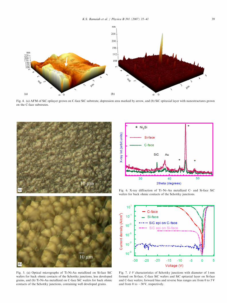
by an optical Nomarski microscope before growth, thesurface contains oval-shape pits i.e., more or less hexagonalshape pattern, some with deep depressions and roughsurface, as shown in Fig. 3a and b, respectively. Fig. 3cshows carrot-like defects with density of 102 cm�2 on theepitaxial layer grown on the C-face 4H-SiC wafer, whichkill the charge carriers in the devices [2]. The depressionsare continued in the SiC epilayer to some extent and thereare several canals and stripes formed in its vicinity asshown in Fig. 4a, which release stress in the layers. TheC-face SiC wafer etched under H2 flow showed peaks andvalleys, which formed due to difference in etching rate byH2. At depressions, the etch rate may be higher. The SiC

ARTICLE IN PRESS
Fig. 1. (a) Optical micrographs of Si-face SiC etched in H2, containing basal plane dislocations (A), micropipes (B), and hexagonal etch pits (C), (b) small
size hexagonal etch pits (A), medium size hexagonal shape etch pits (B), microtubes (C), (c) microtubes with inclusions of microcrystallites (A),
(d) microtubes with inclusion of amorphous structure, and (e) a number of stripes.
K.S. Ramaiah et al. / Physica B 391 (2007) 35–41 37
epitaxial layer grown on the C-face also showed a numberof nano-structures, as shown in Fig. 4b.
The optical microscopy analysis revealed that the (Ti/Ni/Au) metals on the C- and Si-face wafers annealed at1000 1C for back ohmic contacts, showed different grainstructures for the same annealing conditions, as shown inFig. 5a and b for the Si- less developed grains and C-face-
well developed grains, respectively. The C-face is morereactive with metals than that of Si-face. The reason is thatthe surface energy of the C-face is lower than that of Si-faceSiC [19]. The lower surface energy makes the carbon facemore reactive [20]. X-ray diffraction (XRD) analysisrevealed that XRD peaks appeared at 43.651, 45.71, and48.91 indicate Ni2Si phases and other peaks at 35.71 and

ARTICLE IN PRESS
Fig. 2. (a) Atomic force micrographs of Si-face wafer etched in H2, containing micro-tubes, (b) depressed hillock marked by arrow, and (c) SiC epitaxial
layer grown with nano-structures on Si-face substrates.
Fig. 3. (a) Optical micrographs of C-face SiC substrate etched in H2, hexagonal shape pattern, (b) showing depressions with rough surface, and
(c) epilayers grown on the C-face substrates, having carrot like defects.
K.S. Ramaiah et al. / Physica B 391 (2007) 35–4138
38.51 are due to Au and SiC, respectively. Formation ofNi2Si phase is favorable compared to NiSi or NiSi2 phases[21,22]. The XRD intensity of Ni2Si phase is higher in theSi-face than that in the C-face SiC wafer, as shown inFig. 6. It reveals that the formation of Ni2Si phase is muchmore favorable in Si-face than that in the C-face SiC. Nidiffuses quickly and is more reactive with SiC than Ti orAu does [12]. There is no Ti related phase or signalobserved from XRD spectra. It may also be due to
insufficient amount of Ti to detect by XRD. The I–V
studies were carried out on the Ni-Schottky junctions ofC- and Si-face SiC wafers and their epitaxial layers. Thereis no much difference observed in I–V characteristics withor without dislocations in the Schottky junctions formedon the SiC wafer and epitaxial layers under forward bias[23]. However, the leakage current is found to be low in theC-face wafer Schottky junctions, as compared to that in theSi-face wafer Schottky junctions under reverse bias. On the
ARTICLE IN PRESS
Fig. 4. (a) AFM of SiC epilayer grown on C-face SiC substrate, depression area marked by arrow, and (b) SiC epitaxial layer with nanostructures grown
on the C-face substrates.
Fig. 5. (a) Optical micrographs of Ti-Ni-Au metallized on Si-face SiC
wafers for back ohmic contacts of the Schottky junctions, less developed
grains, and (b) Ti-Ni-Au metallized on C-face SiC wafers for back ohmic
contacts of the Schottky junctions, containing well developed grains.
Fig. 6. X-ray diffraction of Ti–Ni–Au metallized C- and Si-face SiC
wafers for back ohmic contacts of the Schottky junctions.
Fig. 7. I–V characteristics of Schottky junctions with diameter of 1mm
formed on Si-face, C-face SiC wafers and SiC epitaxial layer on Si-face
and C-face wafers; forward bias and reverse bias ranges are from 0 to 5V
and from 0 to �30V, respectively.
K.S. Ramaiah et al. / Physica B 391 (2007) 35–41 39

ARTICLE IN PRESSK.S. Ramaiah et al. / Physica B 391 (2007) 35–4140
other hand, the magnitude of the leakage current is lowerin the Schottky junctions formed on the epilayers grown onthe wafers than that in the junctions formed on the wafers,as shown in Fig. 7 [24]. This may be eventually due to thelower density of basal plane dislocations, microtubes,micropipes, pits, screw dislocations, etc., in the epitaxiallayers. In the case of wafer, shallow round pits andtriangular hillocks or depressions may also caused in-creased leakage currents under reverse bias and lowered thebreak down voltage in the I–V measurements [1].
Fig. 8. Schematic diagram of Schottky junction diodes with three different
diameters; B—1.5mm, M—1.0mm, and S—0.5mm.
Table 1
Barrier heights (Fb) of Schottky junctions formed on the typical C-face epitax
Schottky
diode no.
Fb (eV) n (1015-cm�3) Schottky
diode no.
Fb (eV)
B11 1.937 1.459 S11 2.018
B12 1.707 1.705 S12 1.913
B13 1.936 1.457 S13 1.784
B14 1.929 1.572 S14 1.910
B15 1.811 1.671 S15 1.924
B21 1.720 1.622 S16 1.925
B22 2.135 1.291 S17 1.876
B23 2.158 1.199 S21 1.655
B24 2.131 1.291 S22 2.042
B25 1.767 1.354 S23 2.169
S24 2.158
S25 1.980
S26 1.707
S27 1.841
The Schottky junctions fabricated (see Fig. 8 for aschematic diagram) on the epitaxial layers grown on theC-face substrate were studied using C–V method in whichthe calculation of carrier concentration (n), barrier heights(Fb), etc., is given extensively elsewhere [24]. The C–V
mapping studies revealed that the junction barrier height islower in the junctions formed at the edges of the samplesdue to the formation of carrot-like structures, whichdegrade the quality of the layers. The formation ofcarrot-like structures may be due to internal stress whiledepositing the layers because of gas flow turbulence andtemperature gradient at the edges of the samples. Thedensity of hillocks and carrot-like structures is found to bein the range of 102 cm�2, in the epitaxial layer grown on theC-face SiC substrate. The formation of hillocks and carrot-like structures are also due to non-equilibrium condition ofthe Si and C in the reactor that occurs because ofinhomogeneity of C and Si species. In regions of highhillock density and on the other type of defects, the diodesdo not show remarkable differences in the barrier heights.The diodes fabricated on the areas with high density ofcarrot-type structures showed reduced barrier heights ascompared to those do not have any of these defects, asshown in Table 1. The experimentally observed carrierconcentrations and barrier heights of the diodes are nowgiven for the typical sample in Table 1. For example, theedge diodes such as B12, B21, B25, S21, S26, M26, etc.,which contained carrot-like structures, showed lowerbarrier heights. Double- or multi-barriers are not observedin the Schottky diodes unlike those reported in Ref. [23].The triangular shape hillock is assigned to 3C-SiCinclusions in the literature, however Raman studiesrevealed to be 4H-SiC [25]. Therefore further studies arenecessary to confirm the characteristics of hillocks. Wecould not find differences in barrier heights from diode todiode formed on the epilayers grown on the Si-face wafers.Fig. 9 shows the variation of inverse square capacitance
(1/C2) with the voltage (V) for a typical Schottky diode at
ial layers and their carrier concentrations (n) from C–V measurements
n (1015-cm�3) Schottky
diode no.
Fb (eV) n (1015-cm�3)
1.282 M11 1.977 1.550
1.263 M12 1.855 1.234
1.109 M13 1.858 1.216
1.309 M14 1.925 1.323
1.190 M15 1.720 1.622
1.454 M21 2.228 1.701
2.117 M22 2.246 1.790
2.075 M23 2.164 1.697
1.449 M24 2.122 1.647
1.295 M25 2.028 1.485
1.415 M26 1.932 1.488
1.409
1.705
1.598

ARTICLE IN PRESS
Fig. 9. 1/C2 versus V of Schottky diodes on epitaxial layer grown on C-
face SiC wafer at different temperatures, indicating small variation of
capacitance with temperature due to the nature of the SiC semiconductor.
K.S. Ramaiah et al. / Physica B 391 (2007) 35–41 41
different temperatures that reflects the changes in barrierheight with temperature. The typical Ni Schottky barrierheights are found to be 1.93, 1.74, and 1.62 eV attemperatures of 15, 45, and 105 1C, respectively, from theanalysis of 1/C2
�V results. The band gap is predicted to be3.231, 3.224, and 3.210 eV at the respective temperatures[26]. This is based on a zero Kelvin band gap of 3.265 eV[27]. The barrier height decreased with increasing thetemperature. This may be due to the shift in Fermi levelwith activation of shallow carriers due to variation of thetemperature [28,29].
4. Conclusions
H2 etched SiC wafers showed leading basal planedislocations, micropipes, threading edge, and screw edgedislocations. In addition to these dislocations, microtubesand strips are also widely distributed in the wafer. Thedepression area is associated with hillock depressions.Well-developed grains formed when the metals annealed onthe C-face SiC wafer whereas on Si-face those are lessdeveloped, indicating the reaction rate is faster on C-face.Ni2Si is the dominant phase among other phases. Theleakage current of Schottky junctions formed on theepitaxial layer is much less than that on the substrate.The Schottky barrier heights are lower on the carrot-likedefects than that on the regions without defects of theepitaxial layers. The variation of capacitance with tem-perature depends on the activation of shallow carriers evennear room temperature.
References
[1] K.C. Chang, L.M. Porter, J. Bentley, C.Y. Lu, J. Cooper Jr., J. Appl.
Phys. 95 (2004) 8252.
[2] S.T. Kimoto, N. Miyamoto, H. Matsunami, IEEE Trans. Electron
Devices 46 (1999) 471.
[3] Y. Negoro, K. Katsumoto, T. Kimoto, H. Matsunami, J. Appl. Phys.
96 (2004) 224.
[4] U. Forsberga, O. Danielssona, A. Henrya, M.K. Linnarssonb,
E. Janzen, J. Cryst. Growth 236 (2002) 101.
[5] T. Kimoto, N. Inoue, H. Matsunami, Phys. Stat. Sol. (a) 162 (1997)
263.
[6] Y. Ishisa, T. Takahashi, H. Okumura, K. Arai, S. Yoshida, Jpn. J.
Appl. Phys. 43 (2004) 5140.
[7] I. Kamata, H. Tsuchida, T. Jikimoto, K. Izumi, Jpn. Appl. Phys. 41
(2002) L1137.
[8] D.J. Larkin, P.G. Neudeck, J.A. Powell, L.G. Matus, Appl. Phys.
Lett. 65 (1994) 1659.
[9] W. Chen, M.A. Capano, J. Appl. Phys. 98 (2005) 114907.
[10] T. Ohno, H. Yamaguchi, S. Kuroda, K. Kojima, T. Suzuki, K. Arai,
J. Cryst. Growth 271 (2004) 1.
[11] F. Roccaforte, F. La Via, V. Raineri, F. Mangano, L. Calcagno,
Appl. Phys. Lett. 83 (2003) 4181.
[12] F. La Via, F. Roccaforte, A. Makhtari, V. Raineri, P. Musumeci,
L. Calcagno, Microelectron. Eng. 60 (2002) 269.
[13] S.Y. Han, J.-L. Lee, J. Electrochem. Soc. 149 (2002) 189.
[14] A. Castaldini, A. Cavallini, L. Rigutti, S. Pizzini, A. Le Donne,
S. Binetti, J. Appl. Phys. 99 (2006) 033701.
[15] S. Ha, P. Mieszkowski, M. Skowronski, L.B. Rowland, J. Cryst.
Growth 244 (2002) 257.
[16] C. Hallin, F. Owman, P. Martensson, A. Ellison, A. Konstantinov,
O. Kordina, E. Janzen, J. Cryst. Growth 181 (1997) 241.
[17] K.S. Ramaiah, I. Bhat, T.P. Chow, J.K. Kim, E.F. Schubert, Mater.
Sci. Eng. B 129 (2006) 22.
[18] Z. Zhang, T.S. Sudarshan, Appl. Phys. Lett. 87 (2005) 151913.
[19] E. Pearson, T. Takai, T. Halicihogli, W.A. Tiller, J. Cryst. Growth 70
(1984) 33.
[20] M.G. Rastegaeva, A.N. Andreev, A.A. Petrov, A.I. Babanin, M.A.
Yagovkina, M. Yagovkina, I.P. Nikitina, Mater. Sci. Eng. B 46
(1997) 254.
[21] J. Crofton, P.G. Macmullin, J.R. Williams, M.J. Bozak, J. Appl.
Phys. 77 (2003) 1317.
[22] F. La Via, F. Roccaforte, V. Raineri, M. Mauceri, A. Ruggiero,
P. Musumeci, L. Calcagno, A. Castaldini, A. Cavallini, Microelec-
tron. Eng. 70 (2003) 519.
[23] Tumakha, D.J. Ewing, L.M. Porter, Q. Wahab, X. Ma, T.S.
Sudarshan, L.J. Brillson, Appl. Phys. Lett. 87 (2006) 242107.
[24] K.S. Ramaiah, I. Bhat, T.P. Chow, J.K. Kim, E.F. Schubert,
D. Johnstone, S.A-. Biyikli, J. Appl. Phys. 96 (2005) 106108.
[25] W. Si, M. Dudly, H. Kong, J. Sumakeris, C. Carter Jr., J. Electron.
Mat. 26 (1997) 151.
[26] Y. Goldberg, M.E. Levinshtein, S.L. Rumyantsev, Properties of
Advanced Semiconductor Materials GaN, AlN, SiC, BN, SiC, SiG,
Wiley, NewYork, 2001, pp. 93–148.
[27] W.J. Choyke, L. Patrick, D.R. Hamilton, Proceedings of the seventh
International Conference on Semiconductors, Paris, 1964, p. 751.
[28] N. Lundberg, M. Ostling, C.M. Zetterling, P. Tagtstrom, U. Jansson,
J. Electron. Mat. 29 (2000) 372.
[29] C.W. Litton, D. Johnstone, S.A-. Biyikli, K.S. Ramaiah, I. Bhat, T.P.
Chow, J.K. Kim, E.F. Schubert, Appl. Phys. Lett. 88 (2006) 121914.
Copyright © 2022 FDOKUMEN