Supersensitive, Fast-Response Nanowire Sensors by Using Schottky Contacts
6
© 2010 WILEY-VCH Verlag GmbH & Co. KGaA, Weinheim Adv. Mater. 2010, 22, 3327–3332 3327 www.advmat.de www.MaterialsViews.com RESEARCH NEWS By Youfan Hu, Jun Zhou, Ping-Hung Yeh, Zhou Li, Te-Yu Wei, and Zhong Lin Wang* Supersensitive, Fast-Response Nanowire Sensors by Using Schottky Contacts [∗] Dr. Y. F. Hu, Dr. J. Zhou, Dr. P.-H. Yeh, Z. Li, T.-Y. Wei, Prof. Z. L. Wang School of Materials Science and Engineering Georgia Institute of Technology Atlanta, Georgia 30332 (USA) E-mail: [email protected] DOI: 10.1002/adma.201000278 1. Introduction Because of their large surface-to-volume ratios, one-dimensional nanostructures have been regarded as one of the best candidates for realizing ultrasensitive sensors. The most typical configu- ration for gas, chemical, and biochemical nanosensors uses a nanowire (NW) [1–5] or nanotube (NT) [6–10] as the essential building block, bonding two ends of the NW or NT to a solid substrate to fabricate a field-effect transistor (FET). The molecules (detecting target) adsorbed on the surface of the NW or NT may change the device’s conductance by modification of the surface charges and states, disturbing the gate potential, changing the local work function and band alignment, changing the gate coupling, and altering the carrier mobility. All of these can be regarded as a floating gate effect on the conducting channel of the FET, as shown schematically in Figure 1a, which is designed to enhance the contribution made by the nanowire to the final detected signal. In order to furthest enhance the sensitivity of the conduct- ance from the NW or NT, the contacts of the devices are always chosen to be ohmic, for maximizing the gate effect. Typically, thin and usually short nanowires have a higher sensitivity. Recently, the idea of using the Schottky contact to realize supersensitive and fast-response nanowire sensors has been demonstrated in our group for detecting UV light, [11] charged bio-molecules, [12] and different gases. [13] The key to this approach was to construct non-symmetrical Schottky contact devices. The electrical property of the device was then dominantly controlled by the characteristics of the Schottky con- tact. The greatly enhanced sensitivity and response speed of the device indicated that this was a new methodology in the design of nanosensors. 2. Working Principle of the Non-Symmetrical Schottky Contact Device The non-symmetrical Schottky contact device contains a Schottky barrier (SB) contact at one side of the device and an ohmic contact at the other side. The entire device can be regarded as a nanowire connected with a SB diode in series, as shown schematically in Figure 1b. The Schottky contact area is the bottleneck for the current transport in the device. Figure 1c is the energy-band diagram for the Schottky barrier that is formed at the metal-ZnO interface. The original SB height φ SB is determined by the work-function difference between the metal and ZnO, and the interface states. Under a forward bias, the current passing through this barrier can be described by the thermionic-emission theory as: [14] I TE = SA ∗ T 2 exp − q φ SB kT exp qV kT − 1 (1) and, A ∗ = 4π qm ∗ k 2 h 3 (2) in which S is the area of the Schottky contact, A ∗ is the effective Richardson constant, T is the temperature, q is the unit elec- tronic charge, k is the Boltzmann constant, and V is the applied voltage. Under reverse bias, the current can be described by the thermionic-emission-diffusion theory (for V 3kT/q ∼ 77 mV) as: [14] I TED = SA ∗∗ T 2 exp − q φ SB kT × exp 4 q 7 N D (V + V bi − kT/q )/8π 2 ε 3 s kT (3) and, V bi = φ SB − ( E c − E f ) (4) A Schottky barrier can be formed at the interface between a metal electrode and a semiconductor. The current passing through the metal-semiconductor contact is mainly controlled by the barrier height and barrier width. In conventional nanodevices, Schottky contacts are usually avoided in order to enhance the contribution made by the nanowires or nanotubes to the detected signal. We present a key idea of using the Schottky contact to achieve supersensitive and fast response nanowire-based nanosensors. We have illustrated this idea on several platforms: UV sensors, biosensors, and gas sensors. The gigantic enhancement in sensitivity of up to 5 orders of magnitude shows that an effective usage of the Schottky contact can be very beneficial to the sensitivity of nanosensors.
Transcript of Supersensitive, Fast-Response Nanowire Sensors by Using Schottky Contacts

www.advmat.dewww.MaterialsViews.com
RES
EA
Supersensitive, Fast-Response Nanowire Sensors by Using Schottky Contacts
RCH N
By Youfan Hu , Jun Zhou , Ping-Hung Yeh , Zhou Li , Te-Yu Wei , and Zhong Lin Wang *EWS
A Schottky barrier can be formed at the interface between a metal electrode and a semiconductor. The current passing through the metal-semiconductor contact is mainly controlled by the barrier height and barrier width. In conventional nanodevices, Schottky contacts are usually avoided in order to enhance the contribution made by the nanowires or nanotubes to the detected signal. We present a key idea of using the Schottky contact to achieve supersensitive and fast response nanowire-based nanosensors. We have illustrated this idea on several platforms: UV sensors, biosensors, and gas sensors. The gigantic enhancement in sensitivity of up to 5 orders of magnitude shows that an effective usage of the Schottky contact can be very benefi cial to the sensitivity of nanosensors.
1. Introduction
Because of their large surface-to-volume ratios, one-dimensional nanostructures have been regarded as one of the best candidates for realizing ultrasensitive sensors. The most typical confi gu-ration for gas, chemical, and biochemical nanosensors uses a nanowire (NW) [ 1 – 5 ] or nanotube (NT) [ 6 – 10 ] as the essential building block, bonding two ends of the NW or NT to a solid substrate to fabricate a fi eld-effect transistor (FET). The molecules (detecting target) adsorbed on the surface of the NW or NT may change the device’s conductance by modifi cation of the surface charges and states, disturbing the gate potential, changing the local work function and band alignment, changing the gate coupling, and altering the carrier mobility. All of these can be regarded as a fl oating gate effect on the conducting channel of the FET, as shown schematically in Figure 1a , which is designed to enhance the contribution made by the nanowire to the fi nal detected signal. In order to furthest enhance the sensitivity of the conduct-ance from the NW or NT, the contacts of the devices are always chosen to be ohmic, for maximizing the gate effect. Typically, thin and usually short nanowires have a higher sensitivity.
Recently, the idea of using the Schottky contact to realize supersensitive and fast-response nanowire sensors has been demonstrated in our group for detecting UV light, [ 11 ] charged bio-molecules, [ 12 ] and different gases. [ 13 ] The key to this approach
© 2010 WILEY-VCH Verlag GmbH & Co. KGaA, WeinheimAdv. Mater. 2010, 22, 3327–3332
[∗] Dr. Y. F. Hu, Dr. J. Zhou, Dr. P.-H. Yeh, Z. Li, T.-Y. Wei,Prof. Z. L. WangSchool of Materials Science and EngineeringGeorgia Institute of TechnologyAtlanta, Georgia 30332 (USA) E-mail: [email protected]
DOI: 10.1002/adma.201000278
was to construct non-symmetrical Schottky contact devices. The electrical property of the device was then dominantly controlled by the characteristics of the Schottky con-tact. The greatly enhanced sensitivity and response speed of the device indicated that this was a new methodology in the design of nanosensors.
2. Working Principle of the Non-Symmetrical Schottky Contact Device
The non-symmetrical Schottky contact device contains a Schottky barrier (SB) contact at one side of the device and
an ohmic contact at the other side. The entire device can be regarded as a nanowire connected with a SB diode in series, as shown schematically in Figure 1b . The Schottky contact area is the bottleneck for the current transport in the device. Figure 1c is the energy-band diagram for the Schottky barrier that is formed at the metal-ZnO interface. The original SB height φ SB is determined by the work-function difference between the metal and ZnO, and the interface states. Under a forward bias, the current passing through this barrier can be described by the thermionic-emission theory as: [ 14 ]
ITE = SA∗T 2 exp
(−qφSB
kT
)[exp
(q V
kT
)− 1
]
(1)
and,
A∗ = 4πqm∗k2
h3 (2)
in which S is the area of the Schottky contact, A ∗ is the effective Richardson constant, T is the temperature, q is the unit elec-tronic charge, k is the Boltzmann constant, and V is the applied voltage. Under reverse bias, the current can be described by the thermionic-emission-diffusion theory (for V � 3kT/q ∼ 77 mV ) as: [ 14 ]
ITED = SA∗∗T 2 exp(
−qφSB
kT
)
× exp
(4√
q 7 ND(V + Vbi − kT/q )/8π 2ε3s
kT
)
(3)
and,
Vbi = φSB − (Ec − E f ) (4)
3327

3328
RES
EARCH N
EWS
www.advmat.dewww.MaterialsViews.com
Figure 1 . Schematic diagram of the working principle of a nanowire-based nanosensor for a) a conventional FET confi guration and b) the Schottky-gated structure. c) The energy-band diagram at the interface of the metal-ZnO contact, where a Schottky barrier is formed. The barrier height and width can be tuned in response to the change in the sur-rounding environment around the contact area.
in which A ∗ ∗ is the effective Richardson constant, N D is the donor impurity density, V bi is the built-in potential, and ε S is the permittivity of ZnO. The depletion layer formed at the SB area has a width of:
WD =
√2εs
q ND
(Vbi − V − kT
q
)
(5)
Considering Equation 1 , 3 , and 5 we can conclude that the current passing through the Schottky contact is very sensitive to the Schottky barrier height and barrier width, especially under reverse-bias conditions. Light irradiation, adsorbed charged biomolecules, adsorbed gases, etc., at or near the SB area can change the local electric-fi eld distribution, and thus the varia-tion of the SB height and width, resulting in a detectable cur-rent change. This is the working principle of our new device design. We refer to it as a Schottky-gated nanosensor, as sche-matically shown in Figure 1b .
© 2010 WILEY-VCH Verlag G
3. Device Construction
The ZnO NWs used in these experiments were grown by a vapor-solid process. [ 15 ] ZnO powder was used as the precursor and loaded in an alumina boat located at the center of an alumina tube (75 cm), which was placed in a single-zone horizontal tube furnace serving as the reaction chamber. An alumina substrate with a length of 10 cm was loaded 20 cm downstream from the precursor. Argon gas was used as the carrier gas at a fl ow rate of 50 standard cubic centimeters per minute (sccm) throughout the experiment to transport the ZnO vapors downstream for the ZnO NW growth. The furnace was heated to 1475 ° C and held at this temperature for 4.5 h under a pressure of 25 mbar. Then the tube was cooled down to room temperature under an argon fl ow.
For the fabrication of non-symmetrical Schottky contact devices patterned Pt microelectrode arrays were fi rst fabri-cated on the SiO 2 /Si substrate by UV lithography and e-beam evaporation. Then, a single-crystal ZnO NW was placed on a Pt electrode pattern. Finally, a focused ion beam (FIB) system (FEI Nova Nanolab 200 FIB/SEM) was used to deposit Pt-Ga at one end of the ZnO NW on the electrode to make the ohmic contact. The other end formed a natural Schottky contact. The length of the conducting channel between the two electrodes was suffi ciently long to minimize the effect from FIB contami-nation. Figure 2a shows an SEM image and the I-V characteris-tics of a typical Schottky contact device. In order to exhibit the role of the Schottky contact more clearly, devices with an ohmic contact at both ends were also fabricated for comparison, these devices are referred to as ohmic-contact devices. There are two ways to obtain this kind of device. For the following biomolecule- and gas-sensor tests, we used FIB to deposit metal at both ends of the NW to achieve ohmic contacts. For the UV-sensor test, Ti/Au electrodes were deposited on both ends of the NW. The typical I-V curve and a schematic picture of the devices are shown in Figure 2b .
4. UV Sensors
The direct bandgap of 3.4 eV and the large exciton binding energy of 60 meV at room temperature make ZnO a very good candidate for photonics devices working in the UV range.
Various optical applications based on this material have been realized on the nanoscale, including the UV photon detector, [ 16–18 ] optically pumped laser, [ 19 , 20 ] and light-emitting diodes. [ 21 ] For the application of UV photon detectors, a fast response and recovery speed, high responsivity, and high sen-sitivity are commonly desired properties. [ 22 ] Previous research on UV-sensors based on ZnO nanowires have been mostly focused on improving the sensitivity [ 23 , 24 ] and investigating the working mechanism. [ 25 , 26 ] Our experiments [ 11 ] intro-duced the use of non-symmetrical Schottky contact devices, through which the responsivity, response, and recovery speed were greatly improved compared to conventional ohmic-contact devices, which is very important for high-frequency applications.
The photoresponse of the ohmic-contact and Schottky-contact devices are shown in Figure 3 for comparison purposes. Under
mbH & Co. KGaA, Weinheim Adv. Mater. 2010, 22, 3327–3332

RES
EARCH N
EWS
www.advmat.dewww.MaterialsViews.com
Figure 2 . Two types of devices were built for comparison: a) a device with ohmic contact at one end and Schottky contact at the other end, which is called a Schottky-contact device. The upper-left inset shows the SEM image of a typical device after FIB deposition. b) A device with an ohmic contact at both ends of the nanowire, called an ohmic-contact device. The inset shows the two routes to ohmic-contact devices. Reproduced with permission. [ 11–13 ] Copyright 2009, American Institute of Physics.
Figure 3 . a) Photoresponse of a ZnO nanowire ohmic-contact sensor. The inset shows the corresponding I-V properties in the dark and under UV illumination. b) Photoresponse of a ZnO nanowire Schottky-contact sensor. The inset shows the corresponding I-V properties in the dark and under UV illumination. Reproduced with permission. [ 11 ] Copyright 2009, American Institute of Physics.
100
7
10-6
Dark current
0 500 1000 1500 2000 2500 3000
2.65
2.70
2.75
2.80
2.85
2.90
2.95
3.00
3.05
-1.0 -0.5 0.0 0.5 1.0
-3
-2
-1
0
1
2
3
Voltage (v)
Cu
rre
nt
(A
)
Cu
rren
t(
A)
Time (s)
Dark currentUV lumination
0 5 10 15 20 25 30 35 40
0
20
40
60
80
-1.0 -0.5 0.0 0.5 1.0
10-11
10-10
10-9
10-8
10-7
Cu
rre
nt
(A)
Voltage (V)C
urr
en
t(n
A)
Time (s)
UV lumination
UV illumination, in the ohmic-contact case, the photocurrent increases only by about 15%, while a 1500-fold enhancement is observed in the Schottky-contact devices. It must be mentioned that when the Schottky contact is reversely biased the device is more sensitive. Checking the more detailed response process it can be seen that after 260 s of illumination the photocurrent is still not saturated in the ohmic-contact device, whereas a cur-rent change from 0.04 to 60 nA under UV irradiation already occurs within 0.6 s in the Schottky-contact devices. The reset time τ can be used to evaluate the speed of the recovery process, which is defi ned as the time need to recover to 1/e of the max-imum photocurrent. In the ohmic-contact case, the reset time is about 417 s, and in the Schottky-contact case, it is about 0.8 s. Considering all of the above, we can conclude that by utilizing a Schottky contact, the UV sensitivity and response/recovery speed are dramatically enhanced. The strong local electric fi eld at the reversely biased Schottky barrier area will quickly sepa-rate the photon-generated electrons and holes, which reduces the electron-hole recombination rates, resulting in an increase
© 2010 WILEY-VCH Verlag GmAdv. Mater. 2010, 22, 3327–3332
in free carrier density. Also, the UV-illumination-induced desorption of oxygen at the SB changes the barrier height and narrows the barrier width. Both of the above account for the improved UV sensitivity. The more rapid photocurrent response and recovery is related to the fact that when the UV light is turned on or off, the photon-generated electrons and holes in the interface region change quickly, and to modify the SB height the oxygen only needs to be desorbed or readsorbed in the interfacial region, instead of over the whole surface of the nanowire as is the case for ohmic-contact devices. These results demonstrate an effective way for building high-sensitivy and fast-response UV sensors.
5. Biosensors
There is a wide range of applications for biosensors, such as the detection of pathogens, protein engineering, glucose moni-toring in diabetes patients, etc. In order to identify the target molecule, a bioprobe is always used, such as the antibody to the antigen and virus, enzyme to the substrate. [ 27 ] In our work, [ 12 ] by
3329bH & Co. KGaA, Weinheim

3330
RES
EARCH N
EWS
www.advmat.dewww.MaterialsViews.com
Figure 4 . a) The electrical signal of a ZnO nanowire ohmic-contact biosensor when positively charged or negatively charged molecules are introduced. The conductance shows almost no change. b) The response of a Schottky-contact biosensor to negatively charged molecules for a series of concentra-tions. The current variation is quite signifi cant and the response is fast. c) The repeatability of the biosensor. All adapted from the literature. [ 12 ]
introducing a ZnO nanowire, non-symmetrical Schottky-contact device, a probe-free nanosensor can be realized. We used hemo-globin as the sensing molecule. The pH was adjusted to control the molecule to be positively (pI = 7.4 > pH = 5.6) or nega-tively (pI = 7.4 < pH = 8.4) charged. First, we tested the ohmic-contact device. There is no obvious signal when the positively or negatively charged molecules were introduced at a concen-tration of 800 μ g mL − 1 , as shown in Figure 4a . This means that these surface-adsorbed charged molecules do not change the nanowire’s conductance at a detectable degree. Figure 4b shows the fast response and distinct current variation of the Schottky-contact device to the negatively charged molecules for a series of concentrations. In this case, the negatively charged mole-cules that are adsorbed around the SB area do increase the bar-rier height, which results in the observed current decrease. The lowest concentration we have tested is 2 fg mL − 1 . In contrast, when positively charged mole cules are introduced, a current increase was observed. The reproducibility of the device was tested as shown in Figure 4c . The operation of this biosensor is thus largely controlled by the characteristics of the Schottky barrier, and it is very straightforward to differentiate between positively and negatively charged molecules. The sensitivity is high, because only a few adsorbed molecules are needed in the SB area to effectively tune the current passing through the device. We have created a probe-free and highly sensitive NW-
© 2010 WILEY-VCH Verlag G
based biosensor.
6. Gas Sensors
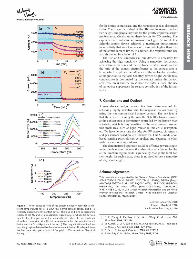
For gas-sensing based on nanomaterials, many methods have been investigated to improve the sensitivity, including surface modifi cation, [ 28 ] using functional material networking, [ 29 ] and designing electrical properties during synthesis. [ 30 ] By using our ZnO NW, non-symmetrical Schottky-contact device, we achieved an enhancement in the sensitivity of several orders of magni-tude over ohmic-contact devices. [ 12 ] For oxygen detection an O 2 atmosphere was introduced as 10 wt% O 2 in N 2 . The response curves to the oxygen at different temperatures, ranging from 150 to 300 ° C, were recorded for the ohmic contact device and reversely biased Schottky-contact device, as shown, respec-tively, in Figure 5a and 5b . The sensitivity was defi ned as Δ I/I 0 , where Δ I is the current change induced by the exposure of the device to the target gas atmosphere, and I 0 is the original cur-rent. The oxygen molecules adsorbed at the ZnO NW surface will capture the electrons in the NW, and reduce the conduct-ance of the NW. The highest sensitivity of only 4.8% for the ohmic-contact device was achieved at 275 ° C with a response time constant of 209 s. This indicates that the surface adsorp-tion of negatively charged oxygen ions only results in a minor change in the inherent conductance of the ZnO NW. For the reversely biased Schottky-contact device, the highest sensitivity is 3235%, which was achieved at 250 ° C, with a response time constant of 30 s. The sensitivity is 1085 times higher than that
mbH & Co. KGaA, Weinheim Adv. Mater. 2010, 22, 3327–3332
RES
EARCH N
EWS
www.advmat.dewww.MaterialsViews.com
© 2010 WILEY-VCH Verlag GmAdv. Mater. 2010, 22, 3327–3332
0 5 10 15 20
4000
4250
4500
300oC
275oC
250oC
200oC
175oC
150oC
Cu
rre
nt
(nA
)
Time (min)
4
0 5 10 15
0
-2000
-4000
-6000
Cu
rre
nt
(nA
)
Time (min)
150oC
175oC
200oC
250oC
275oC
300oC
150 200 250 300
0
8000
16000
24000
32000
Sen
sit
ivit
y(%
)
Temperature (oC)
Reversely biased Schottky
contact device
50ppm 100ppm
200ppm 300ppm
400ppm
Ohmic contact device
50ppm 100ppm
200ppm 300ppm
400ppm
150 200 250 300
0
1
2
3
4
Se
ns
itiv
ity
(%)
Temperature (oC)
50ppm
100ppm
200ppm
300ppm
400ppm
Figure 5 . The response current of the oxygen detection recorded at dif-ferent temperatures for a) a ZnO NW ohmic-contact device, and b) a reversely biased Schottky-contact device. The blue and pink backgrounds represent the N 2 and O 2 atmosphere, respectively, in which the devices were kept. c) Comparison of the sensitivity with different concentrations of carbon monoxide at different temperatures for the ohmic-contact device and the Schottky-contact device. d) The magnifi cation of the low-sensitivity region detected by the ohmic-contact device. All adapted from the literature, with permission. [ 13 ] Copyright 2009, American Chemical Society.
for the ohmic-contact case, and the response speed is also much faster. The oxygen adsorbed at the SB area increases the bar-rier height, and plays a key role for the greatly improved sensor performance. We also tested these devices for CO sensing. The experimental results are summarized in Figure 5c and d . The Schottky-contact device achieved a maximum enhancement in sensitivity that was 4 orders of magnitude higher than that of the ohmic-contact device. In addition, the response time was also shortened by a factor of 7.
The use of fi ne nanowires in our devices is necessary for achieving the high sensitivity. Using a nanowire, the contact area between the NW and the electrode is rather small, so that the ratio of the contact circumference to the contact area is large, which amplifi es the infl uence of the molecules adsorbed at the junction to the local Schottky barrier height. As the total conductance is dominated by the contact inside the contact area (core area) and the areas near the outer surface, the use of nanowires suppresses the relative contribution of the former factor.
7. Conclusions and Outlook
A new device design concept has been demonstrated for achieving highly sensitive and fast-response nanosensors by using the non-symmetrical Schottky contact. The key idea is that the current passing through the Schottky barrier formed at the contact area is dominantly controlled by the barrier char-acteristic, which is very sensitive to the environment around this small area, such as light irradiation, molecule adsorption, etc. We have demonstrate this idea for UV sensors, biosensors, and gas sensors based on ZnO nanowires. This SB-modulation based sensing principle can be applied and extended to other materials and sensing systems.
The demonstrated approach could be effective toward single-molecule detection, because the adsorption of a few molecules at the junction region could signifi cantly change the local bar-rier height. In such a case, there is no need to use a nanowire of very short length.
Acknowledgements This research was supported by the National Science Foundation (NSF) (DMS 0706436, CMMI 0403671, ENG/CMMI 112024), DARPA (Army/AMCOM/REDSTONE AR, W31P4Q-08-1-0009), BES DOE (DE-FG02-07ER46394), Air Force Offi ce (FA9550-08-1-0446), DARPA/ARO W911NF-08-1-0249, KAUST Global Research Partnership, and the World Premier International Research Center (WPI) Initiative on Materials Nanoarchitectonics, MEXT, Japan.
Received: January 25, 2010 Revised: March 31, 2010
Published online: May 5, 2010
[ 1 ] G. F. Zheng , F. Patolsky , Y. Cui , W. U. Wang , C. M. Lieber , Nat. Biotechnol. 2005 , 23 , 1294 .
[ 2 ] M. Curreli , C. Li , Y. Sun , B. Lei , M. A. Gundersen , M. E. Thompson , C. Zhou , J. Am. Chem. Soc. 2005 , 127 , 6922 .
[ 3 ] Z. Fan , J. G. Lu , Appl. Phys. Lett. 2005 , 86 , 123510 . [ 4 ] F. Patolsky , C. M. Lieber , Mater. Today 2005 , 8 , 20 .
3331bH & Co. KGaA, Weinheim

3332
RES
EARCH N
EWS
www.advmat.dewww.MaterialsViews.com
[
[
[ [
[ [ [
[
[ 5 ] J. H. He , Y. Y. Zhang , J. Liu , D. Moore , G. Bao , Z. L. Wang , J. Phys. Chem. C 2007 , 111 , 12152 .
[ 6 ] R. J. Chen , H. C. Choi , S. Bangsaruntip , E. Yenilmez , X. Tang , Q. Wang , Y. L. Chang , H. Dai , J. Am. Chem. Soc. 2004 , 126 , 1563 .
[ 7 ] A. B. Artyukhin , M. Stadermann , R. W. Friddle , P. Stroeve , O. Bakajin , A. Noy , Nano Lett. 2006 , 6 , 2080 .
[ 8 ] X. Tang , S. Bansaruntip , N. Nakayama , E. Yenilmez , Y. L. Chang , Q. Wang , Nano Lett. 2006 , 6 , 1632 .
[ 9 ] E. L. Gui , L. J. Li , K. Zhang , Y. Xu , X. Dong , X. Ho , P. S. Lee , J. Kasim , Z. X. Shen , J. A. Rogers , S. G. Mhaisalkar , J. Am. Chem. Soc. 2007 , 129 , 14427 .
10 ] I. Heller , A. M. Janssens , J. Männik , E. D. Minot , S. G. Lemay , C. Dekker , Nano Lett. 2008 , 8 , 591 .
11 ] J. Zhou , Y. D. Gu , Y. F. Hu , W. J. Mai , P.-H. Yeh , G. Bao , A. K. Sood , D. L. Polla , Z. L. Wang , Appl. Phys. Lett. 2009 , 94 , 191103 .
12 ] P.-H. Yeh , Z. Li , Z. L. Wang , Adv. Mater. 2009 , 21 , 4975 . 13 ] T.-Y. Wei , P.-H. Yeh , S.-Y. Lu , Z. L. Wang , J. Am. Chem. Soc. 2009 ,
131 , 17 690 . 14 ] S. M. Sze , Physics of Semiconductor Devices Wiley , New York, NY 1981 . 15 ] Z. W. Pan , Z. R. Dai , Z. L. Wang , Science 2001 , 291 , 1947 . 16 ] H. Kind , H. Q. Yan , B. Messer , M. Law , P. D. Yang , Adv. Mater. 2002 ,
14 , 158 . 17 ] C. Soci , A. Zhang , B. Xiang , S. A. Dayeh , D. P. R. Aplin , J. Park , X. Y.
Bao , Y. H. Lo , D. Wang , Nano Lett. 2007 , 7 , 1003 .
© 2010 WILEY-VCH Verlag Gm
[ 18 ] Y. Z. Jin , J. P. Wang , B. Q. Sun , J. C. Blakesley , N. C. Greenham , Nano Lett. 2008 , 8 , 1649 .
[ 19 ] M. H. Huang , S. Mao , H. Feick , H. Q. Yan , Y. Y. Wu , H. Kind , E. Weber , R. Russo , P. D. Yang , Science 2001 , 292 , 1897 .
[ 20 ] R. X. Yan , D. Gargas , P. D. Yang , Nat. Photonics 2009 , 3 , 569 . [ 21 ] Y. Ryu , T. S. Lee , J. A. Lubguban , H. W. White , B. J. Kim , Y. S. Park ,
Appl. Phys. Lett. 2006 , 88 , 241108 . [ 22 ] L. Luo , Y. F. Zhang , S. S. Mao , L. W. Lin , Sens. Actuators A 2006 , 127 ,
201 . [ 23 ] C. S. Lao , M. C. Park , Q. Kuang , Y. Deng , A. K. Sood , D. L. Polla ,
Z. L. Wang , J. Am. Chem. Soc. 2007 , 129 , 12096 . [ 24 ] R. S. Aga , D. Jowhar , A. Ueda , Z. Pan , W. E. Collins , R. Wu , K. D.
Singer , J. Shen , Appl. Phys. Lett. 2007 , 91 , 232108 . [ 25 ] S. E. Ahn , H. J. Ji , K. Kim , G. T. Kim , C. H. Bae , S. M. Park , Y. K. Kim ,
J. S. Ha , Appl. Phys. Lett. 2007 , 90 , 153106 . [ 26 ] Y. B. Li , F. D. Valle , M. Simonnet , I. Yamada , J. J. Delaunay , Appl.
Phys. Lett. 2009 , 94 , 023110 . [ 27 ] K. Maehashi , T. Katsura , K. Kerman , Y. Takamura , K. Matsumoto ,
E. Tamiya , Anal. Chem. 2007 , 79 , 782 . [ 28 ] J. H. He , C. H. Ho , C. Y. Chen , Nanotechnology 2009 , 20 , 065503 . [ 29 ] Y. Wang , G. Du , H. Liu , D. Liu , S. Qin , N. Wang , C. Hu , X. Tao ,
J. Jiao , J. Wang , Z. L. Wang , Adv. Funct. Mater. 2008 , 18 , 1131 . [ 30 ] M. W. Ahn , K. S. Park , J. H. Heo , J. G. Park , D. W. Kim , K. J. Choi ,
J. H. Lee , S. H. Hong , Appl. Phys. Lett. 2008 , 93 , 263103 .
bH & Co. KGaA, Weinheim Adv. Mater. 2010, 22, 3327–3332