Schottky Junctions in Thin-Film Electronic Devices
201
Schottky Junctions in Thin-Film Electronic Devices A thesis submitted to the University of Manchester for the degree of Doctor of Philosophy in the Faculty of Science and Engineering 2018 Joshua M Wilson School of Electrical and Electronic Engineering
-
Upload
khangminh22 -
Category
Documents
-
view
0 -
download
0
Transcript of Schottky Junctions in Thin-Film Electronic Devices
Schottky Junctions in Thin-FilmElectronic Devices
A thesis submitted to the University of Manchester for the degree of
Doctor of Philosophy
in the Faculty of Science and Engineering
2018
Joshua M Wilson
School of Electrical and Electronic Engineering
Contents
List of Symbols 6
List of Abbreviations 13
List of Figures 14
List of Tables 26
Abstract 27
Declaration 28
Copyright Statement 29
Acknowledgements 30
About the Author 31
1 Introduction 32
1.1 Background and Motivation . . . . . . . . . . . . . . . . . . . . . 32
1.2 Aims and Objectives . . . . . . . . . . . . . . . . . . . . . . . . . 35
1.3 Thesis Structure . . . . . . . . . . . . . . . . . . . . . . . . . . . . 36
2 Background: Materials and Devices 37
2.1 Oxide Semiconductors . . . . . . . . . . . . . . . . . . . . . . . . 37
2.1.1 Introduction . . . . . . . . . . . . . . . . . . . . . . . . . . 37
2.1.2 General Properties . . . . . . . . . . . . . . . . . . . . . . 38
2.1.3 Zinc Oxide (ZnO) . . . . . . . . . . . . . . . . . . . . . . . 40
2.1.4 Indium Gallium Zinc Oxide (IGZO) . . . . . . . . . . . . . 41
2.2 Schottky Contacts . . . . . . . . . . . . . . . . . . . . . . . . . . 47
2.2.1 Introduction . . . . . . . . . . . . . . . . . . . . . . . . . . 47
2.2.2 Depletion Approximation . . . . . . . . . . . . . . . . . . . 48
2.2.3 Image Force Lowering . . . . . . . . . . . . . . . . . . . . 51
2.2.4 Thermionic Emission . . . . . . . . . . . . . . . . . . . . . 52
2

2.2.5 Diffusion Theory . . . . . . . . . . . . . . . . . . . . . . . 55
2.2.6 Barrier Height Inhomogeneities . . . . . . . . . . . . . . . 57
2.2.7 IGZO Schottky Diodes . . . . . . . . . . . . . . . . . . . . 60
2.3 Standard Thin Film Transistors (TFTs) . . . . . . . . . . . . . . 62
2.3.1 Introduction . . . . . . . . . . . . . . . . . . . . . . . . . . 62
2.3.2 Operating Mechanism . . . . . . . . . . . . . . . . . . . . 62
2.3.3 TFT Parameters . . . . . . . . . . . . . . . . . . . . . . . 66
2.3.4 IGZO TFTs . . . . . . . . . . . . . . . . . . . . . . . . . . 69
2.3.5 Applications . . . . . . . . . . . . . . . . . . . . . . . . . . 71
2.4 Schottky Source Transistors (SSTs) . . . . . . . . . . . . . . . . . 73
2.4.1 Introduction . . . . . . . . . . . . . . . . . . . . . . . . . . 73
2.4.2 Operating Mechanism . . . . . . . . . . . . . . . . . . . . 73
2.4.3 Considerations for Device Design . . . . . . . . . . . . . . 78
2.4.4 Advantages and Disadvantages . . . . . . . . . . . . . . . 80
2.4.5 Applications . . . . . . . . . . . . . . . . . . . . . . . . . . 81
2.4.6 IGZO SSTs . . . . . . . . . . . . . . . . . . . . . . . . . . 82
3 Thickness Dependence in Thin-Film Schottky Diodes 83
3.1 IGZO Schottky Diodes with Different Thicknesses . . . . . . . . . 84
3.2 Possible Reasons for Thickness Dependence . . . . . . . . . . . . 87
3.2.1 Diffusion Theory . . . . . . . . . . . . . . . . . . . . . . . 88
3.2.2 Image Force Lowering . . . . . . . . . . . . . . . . . . . . 89
3.2.3 Tunnelling . . . . . . . . . . . . . . . . . . . . . . . . . . . 91
3.2.4 Anode Roughness . . . . . . . . . . . . . . . . . . . . . . . 92
3.2.5 Inhomogeneous Barrier Height . . . . . . . . . . . . . . . . 94
3.3 Effects of Barrier Height Inhomogeneities on Forward Current . . 99
3.3.1 Barrier Height . . . . . . . . . . . . . . . . . . . . . . . . . 99
3.3.2 Ideality Factor . . . . . . . . . . . . . . . . . . . . . . . . 100
3.4 Multiple Inhomogeneities . . . . . . . . . . . . . . . . . . . . . . . 102
3.5 Summary . . . . . . . . . . . . . . . . . . . . . . . . . . . . . . . 106
3

4 Analytical Theory of Thin-Film Schottky Diodes 108
4.1 Potential in a Thin-Film Schottky Diode . . . . . . . . . . . . . . 109
4.1.1 Image Force Lowering . . . . . . . . . . . . . . . . . . . . 111
4.2 Current Transport in Fully Depleted Thin-Film Schottky Diodes . 112
4.2.1 Thermionic Emission Current . . . . . . . . . . . . . . . . 112
4.2.2 Diffusion Current . . . . . . . . . . . . . . . . . . . . . . . 113
4.3 Theory of Inhomogeneities in Thin-Film Diodes . . . . . . . . . . 115
4.3.1 Potential . . . . . . . . . . . . . . . . . . . . . . . . . . . . 116
4.3.2 Thermionic Emission Current . . . . . . . . . . . . . . . . 119
4.3.3 Diffusion Current . . . . . . . . . . . . . . . . . . . . . . . 124
4.4 Multiple Inhomogeneities . . . . . . . . . . . . . . . . . . . . . . . 127
4.4.1 Potential . . . . . . . . . . . . . . . . . . . . . . . . . . . . 127
4.4.2 Thermionic Emission Current . . . . . . . . . . . . . . . . 129
4.5 Summary . . . . . . . . . . . . . . . . . . . . . . . . . . . . . . . 133
5 Schottky Source Transistors: Design, Theory and Applications 135
5.1 Control of the Source Barrier . . . . . . . . . . . . . . . . . . . . 136
5.1.1 Schottky Contacts on Oxides: Important Considerations . 136
5.1.2 Experimental Results for Schottky Diodes . . . . . . . . . 137
5.1.3 Experimental Results for SSTs . . . . . . . . . . . . . . . . 139
5.1.4 X-Ray Photoelectron Spectroscopy of Pt Films . . . . . . . 141
5.2 Thickness Dependence of SST Behaviour . . . . . . . . . . . . . . 143
5.3 Effects of Barrier Inhomogeneities . . . . . . . . . . . . . . . . . . 145
5.3.1 Explaining the Experimental I-V Curves . . . . . . . . . . 147
5.3.2 Replicating Semiconductor Thickness Dependence . . . . . 150
5.3.3 Inhomogeneity Magnitude and Position . . . . . . . . . . . 153
5.3.4 Effect of Barrier Inhomogeneities on Saturation Voltage . . 155
5.4 Analytical Theory . . . . . . . . . . . . . . . . . . . . . . . . . . . 157
5.5 Intrinsic Gain . . . . . . . . . . . . . . . . . . . . . . . . . . . . . 161
5.6 Short Channel Effect . . . . . . . . . . . . . . . . . . . . . . . . . 163
5.7 Negative Bias Illumination Temperature Stress . . . . . . . . . . . 164
5.8 Application to Other Oxide Materials . . . . . . . . . . . . . . . . 165
4
5.9 Summary . . . . . . . . . . . . . . . . . . . . . . . . . . . . . . . 166
6 Conclusions and Future Prospects 168
6.1 Conclusions . . . . . . . . . . . . . . . . . . . . . . . . . . . . . . 168
6.2 Future Prospects . . . . . . . . . . . . . . . . . . . . . . . . . . . 171
A Device Simulation 173
A.1 Input Deck . . . . . . . . . . . . . . . . . . . . . . . . . . . . . . 173
A.1.1 Mesh . . . . . . . . . . . . . . . . . . . . . . . . . . . . . . 173
A.1.2 Regions and Electrodes . . . . . . . . . . . . . . . . . . . . 174
A.1.3 Doping . . . . . . . . . . . . . . . . . . . . . . . . . . . . . 174
A.1.4 Material . . . . . . . . . . . . . . . . . . . . . . . . . . . . 174
A.1.5 Density of States . . . . . . . . . . . . . . . . . . . . . . . 175
A.1.6 Contact . . . . . . . . . . . . . . . . . . . . . . . . . . . . 176
A.1.7 Models . . . . . . . . . . . . . . . . . . . . . . . . . . . . . 177
A.1.8 Output . . . . . . . . . . . . . . . . . . . . . . . . . . . . . 177
A.1.9 Solve . . . . . . . . . . . . . . . . . . . . . . . . . . . . . . 178
A.1.10 DBInternal . . . . . . . . . . . . . . . . . . . . . . . . . . 178
A.2 Equations Solved in Atlas . . . . . . . . . . . . . . . . . . . . . . 179
A.3 TonyPlot . . . . . . . . . . . . . . . . . . . . . . . . . . . . . . . . 180
References 181
Word Count: 37,200
5

List of Symbols
A Area (cm2).
A∗ Richardson constant (A cm−2 K−2).
A1 Area of Schottky barrier region with barrier height φ0B (cm2).
A2 Area of Schottky barrier region with barrier height φ0B −∆ (cm2).
Aeff The effective area of the low barrier region (cm2).
Av Intrinsic gain.
c Quasi-density parameter for low barrier regions (V−1/2 cm−1/2).
C Capacitance per unit area (F cm−2).
CD Capacitance per unit area of the Depletion Layer (F cm−2).
CG Capacitance per unit area of the gate dielectric (F cm−2).
CS Capacitance per unit area of the semiconductor (F cm−2).
Dn Diffusion coefficient for electrons (cm2 s−1).
Dp Diffusion coefficient for holes (cm2 s−1).
DSG Subgap density of states (cm−3 eV−1).
E Energy or work done (eV).
EC Conduction band minimum (eV).
ECM Maximum of EC beneath the centre of the inhomogeneity/low barrier
region (eV).
EF Fermi energy (eV).
EFn Quasi-Fermi energy in an n-type semiconductor (eV).
EGD Energy of Gaussian distributed donor peak (eV).
EN Fermi energy from the conduction band edge in an n-type semicon-
ductor (EC − EF ) (eV).
EV Valence band maximum (eV).
E Electric field (V/cm).
E Electric field vector (V/cm).
EM Maximum electric field in a Schottky diode under the standard de-
pletion approximation (V/cm).
6
EMT Maximum electric field in a fully depleted thin-film Schottky diode
(V/cm).
EMT1 Maximum electric field in the region of the Schottky diode with bar-
rier height φ0B (V/cm).
EMT2 Maximum electric field in the region of the Schottky diode with bar-
rier height φ0B −∆ in the absence of a saddle point (V/cm).
EMTS Maximum electric field in the region of the Schottky diode with bar-
rier height φ0B −∆ in the presence of a saddle point (V/cm).
F Force (N).
F (E) Distribution function.
gd Output conductance (S).
gGA(E) Gaussian distributed acceptor states (cm−3 eV−1).
gGD(E) Gaussian distributed donor states (cm−3 eV−1).
gm Transconductance (S).
Gn Generation rate for electrons (cm−3 s−1).
Gp Generation rate for holes (cm−3 s−1).
gTA(E) Acceptor tails states (cm−3 eV−1).
gTD(E) Donor tails states (cm−3 eV−1).
h Planck constant (J s).
H Semiconductor thickness (cm).
HT Anode tooth height (cm).
i Unit vector in the x-direction.
I Current (A).
I1 Current injected from the region close to the source edge nearest the
drain in an SST (A).
I2 Current injected from the region away from source edge in an SST
(A).
ID Drain current (A).
IDlin Drain current in the linear regime (A).
7

IDsat Drain current in the saturation regime (A).
Iline Current through the low barrier region in the dipole line Schottky
diode model (A).
Isheet Current through the low barrier region in the dipole sheet Schottky
diode model (A).
J Current density (A cm−2).
J Current density vector (A cm−2).
Jn Current density vector for electrons (A cm−2).
Jp Current density vector for holes (A cm−2).
JR Reverse current density (A cm−2).
Js→m Current density from the semiconductor to the metal (A cm−2).
JV Current density vertically from the source to the semiconductor-
dielectric interface (A cm−2).
Jz Current density in the z-direction (A cm−2).
k Boltzmann constant = 1.38× 10⁻²³ (J/K).
k Unit vector in the z-direction.
L Channel length.
L0 Width of inhomogeneity/low barrier region (cm).
Leff Effective contact length (cm).
Lx Diode width (cm).
Ly Diode length (cm).
m∗ Effective mass of an electron (kg).
me Rest mass of an electron (kg).
n Ideality Factor.
N(E) Density of states (cm−3 eV−1).
NC Effective density of states in the conduction band (cm−3).
ND Donor density (cm−3).
ne Free electron concentration (cm−3).
NGD Total density of donor-like states in a Gaussian distribution
(cm−3 eV−1).
8

Nint Electron density along the semiconductor-dielectric interface (cm−3).
NTA Density of acceptor-like states in the tail distribution at the conduc-
tion band minimum (cm−3 eV−1).
NTD Density of donor-like states in the tail distribution at valence band
maximum (cm−3 eV−1).
P Distance from the source edge (cm).
pA Dipole moment per unit area (C cm−1).
p Dipole moment (C cm).
ph Free hole concentration (cm−3).
pL Dipole moment per unit length (C).
P (θ) Probability density function for the Gamma distribution.
q Fundamental charge (C).
Q Charge per unit area (C cm−2).
Qind Induced charge per unit area (C cm−2).
Rint Resistance along the semiconductor-dielectric interface (Ω).
Rn Recombination rate for electrons (cm−3 s−1).
ro Output resistance (Ω).
Rp Recombination rate for holes (cm−3 s−1).
RV Vertical resistance between the semiconductor-dielectric interface and
the source contact (Ω).
S Source length (cm).
SS Subthreshold swing (V/dec).
T Temperature (K).
t Time (s).
V Applied voltage (V).
v Carrier velocity (cm/s).
v0z Carrier velocity required to overcome a Schottky barrier (cm/s).
vD Diffusion velocity (cm/s).
VD Drain voltage (V).
9

VDsat1 Saturation voltage in a Schottky source transistor (V).
VDsat2 Saturation voltage in an thin-film transistor (V).
VG Gate voltage (V).
Vint Potential at the semiconductor-dielectric interface (V).
VON On voltage of a thin-film transistor (V).
vR Recombination velocity (cm/s).
VT Threshold voltage of a thin-film transistor (V).
VTS Threshold voltage of a Schottky source transistor (V).
vz Electron velocity in the z-direction (cm/s).
W Channel width (cm).
WD Depletion width of a Schottky junction (cm).
WGD Characteristic decay energy for the Gaussian distribution of donor-
like states (eV).
WT Anode tooth width (cm).
WTA Characteristic decay energy for the tail distribution of acceptor-like
states (eV).
WTD Characteristic decay energy for the tail distribution of donor-like
states (eV).
x Distance in the x-direction (cm).
y Distance in the y-direction (cm).
z Distance in the z-direction (cm).
zmax Position of barrier height maximum formed due to image force low-
ering (cm).
zs Saddle point position (cm).
α Empirical quantity denoting the dependence of the barrier height on
the electric field (cm).
β Image force lowering coefficient in Silvaco Atlas.
γ Variable in Silvaco Atlas denoting the power that electric field is
raised to when calculating barrier lowering.
10
Γ Gamma function.
δ Difference between the mean barrier height and the barrier height of
the inhomogeneity/low barrier region (V).
∆ Difference between the mean barrier height and the barrier height of
the inhomogeneity/low barrier region (eV).
ε0 Permittivity of free space (8.85× 10⁻¹⁴ (F/cm).
εs Relative permittivity of the semiconductor.
θ Combined inhomogeneity parameter (V1/2 cm1/2).
µLIN TFT mobility extracted from the linear regime (cm2/Vs).
µn Electron mobility in an n-type semiconductor (cm2/Vs).
µp Electron mobility in a p-type semiconductor (cm2/Vs).
µSAT TFT mobility extracted from the saturation regime (cm2/Vs).
ξ Measure of the width of the θ distribution (V1/2 cm1/2).
ρ Charge density (C cm−3).
ρV Resistivity vertically from the source to the semiconductor-dielectric
interface (Ω cm).
σ Electrical conductivity (S/m).
σint Conductivity along the semiconductor-dielectric interface (S/m).
φ Electrostatic potential (V).
φB Schottky barrier height (V).
ΦB Schottky barrier height (eV).
φ0B Mean Schottky barrier height potential (V).
Φ0B Mean Schottky barrier height (eV).
φB,D Schottky barrier height extracted using diffusion theory (V).
φB,eff The effective barrier height of the low barrier region (V).
ΦB,eff Effective Schottky barrier height (eV).
φbi Built-in potential of a Schottky junction (V).
φBL Silvaco barrier lowering potential (V).
φB,TFD Schottky barrier height extracted using thin-film diffusion theory (V).
11

φd Dipole potential (V).
φIFL Reduction in barrier height due to image force lowering (V).
ΦIFL Reduction in barrier height due to image force lowering (eV).
φline Potential due to the dipole line (V).
ΦM Work function of a metal (eV).
φn Fermi potential from the conduction band edge in an n-type semi-
conductor (EC − EF )/q (V).
ΦSC Work function of a semiconductor (eV).
φsheet Potential due to the dipole sheet (V).
χSC Electron affinity of a semiconductor (eV).
ψ Difference between the local and mean Schottky barrier heights (V).
12

List of Abbreviations
2D Two-dimensional.
AMLCD Active matrix liquid crystal display.
AMOLED Active matrix organic light emitting diode.
a-Si:H Amorphous hydrogenated silicon.
HBR High barrier region of the Schottky contact.
IFL Image force lowering.
IGZO Indium gallium zinc oxide.
ITO Indium tin oxide.
IZO Indium zinc oxide.
LBR Low barrier region of the Schottky contact.
LCD Liquid crystal display.
LED Light emitting diode.
LTPS Low temperature polycrystalline silicon.
MESFET Metal semiconductor field effect transistor.
MISFET Metal insulator semiconductor field effect transistor.
NBITS Negative bias illumination temperature stress.
OLED Organic light emitting diode.
PET Polyethylene terephthalate.
PLD Pulsed laser deposition.
RF Radio frequency.
RFID Radio frequency identification.
SST Schottky source transistor.
TCO Transparent conducting oxide.
TFT Thin-film transistor.
UST Universal Schottky tunnelling.
XPS X-ray photoelectron spectroscopy.
13

List of Figures
2.1 Electron configurations of both Si (left) and metal oxides, such as
IGZO, (right) in both crystalline and amorphous phases. Adapted
from [10]. . . . . . . . . . . . . . . . . . . . . . . . . . . . . . . . 38
2.2 Transparent flexible IGZO TFTs fabricated by Nomura et al. in
2004. The devices are only visible due to the angle of illumination.
Taken from [10]. . . . . . . . . . . . . . . . . . . . . . . . . . . . . 42
2.3 Effects of variations in In:Ga:Zn ratio upon (a) field effect mobility
and (b) on voltage, for deposition with 0.4% oxygen and annealed
at 150 °C. Taken from [7]. . . . . . . . . . . . . . . . . . . . . . . 45
2.4 Percolation conduction over a spatially varying random distribu-
tion of potential barriers in the conduction band minimum. Elec-
tron (a) has greater energy, taking a higher shorter path than elec-
tron (b). Adapted from [103]. . . . . . . . . . . . . . . . . . . . . 47
2.5 Schottky barrier formation. (a) A metal and an n-type semicon-
ductor are brought under the condition ΦM > ΦSC . (b) Band
diagram for a standard Schottky diode with the semiconductor
thickness larger than the depletion width WD. . . . . . . . . . . . 49
2.6 Comparison of the simulated results of a homogeneous Schot-
tky barrier to the values predicted by the depletion approxima-
tion. The simulated Schottky diode had a semiconductor thickness
H > 2WD. (a) Cutline of the conduction band energy between the
barrier and the depletion width. (b) Cutline displaying the abso-
lute value of the electric field between the barrier and the depletion
width. . . . . . . . . . . . . . . . . . . . . . . . . . . . . . . . . . 51
2.7 Schematic of how image force lowering forms a saddle point in the
barrier height. . . . . . . . . . . . . . . . . . . . . . . . . . . . . . 52
2.8 Schottky diode characteristics. (a) How to extract ΦB and n from
|J |-V characteristics. (b) How to extract ND from C−2-V charac-
teristics. . . . . . . . . . . . . . . . . . . . . . . . . . . . . . . . . 54
14
2.9 |J |-V characteristics for thermionic emission theory and a simu-
lated diode with µ = 106 cm2/Vs. Such a large semiconductor
mobility must be used as the theory assumes an infinite mobility. 55
2.10 Metal work function dependence upon crystal orientation for cop-
per, from [139]. Topography (a) and work function (b) were ob-
tained using Kelvin probe force microscopy. In (b) H, M and L
stand for high, medium and low work function respectively. The
crystal orientation (c) was obtained using electron back scattered
diffraction. . . . . . . . . . . . . . . . . . . . . . . . . . . . . . . . 57
2.11 Geometry of the dipole sheet approximation and related simulations. 59
2.12 Four potential structures for TFTs. Taken from [7]. . . . . . . . . 63
2.13 Behaviour of an n-type TFT. (a) Electron concentration for a sim-
ulated IGZO TFT in the linear region (VG− VT >> VD). The low
value of VD means that the channel is accumulated evenly at the
semiconductor-dielectric interface. (b) Electron concentration for
a simulated IGZO TFT in the saturation region (VG − VT ≤ VD).
At high enough VD (∼ VG − VT ) the channel is pinched-off at the
drain edge. (c) Output curves for an IGZO TFT showing the linear
and saturation regions. (d) Transfer curves for an IGZO TFT in
saturation. On/off ratio and VON are extracted from the log scale
curve (black) and VT is extracted from the I1/2D -VG curve (blue).
Black and blue arrows indicate direction of hysteresis. . . . . . . 64
2.14 Distributed diode and resistor network model for a Schottky source
transistor, proposed by Valletta et al. [222]. . . . . . . . . . . . . 74
2.15 Simulated output curves of an SST with its three separate regions
“initial jump”, linear and saturation. The devices have a IGZO
and SiO2 thicknesses of 100 nm. The source, channel and drain
are 5, 2 and 1µm long, respectively, and the gate overlaps all of
these regions. The Schottky contact at the source has a barrier
height of 0.5 eV and the IGZO is modelled on the work of Fung et
al. [119], see Appendix A.1.5. . . . . . . . . . . . . . . . . . . . . 75
15

2.16 Behaviour of current density under the source when in the linear
region. (a) The linear increase with VD. (b) Injection area increas-
ing and then current injection saturating with increasing VG. . . . 76
2.17 Electron concentration in the semiconductor of an SST where
VG = 10 V. (a) When VD < VDsat1. (b) When VD > VDsat1
and the semiconductor-dielectric interface is pinched-off beneath
the drain end of the source. . . . . . . . . . . . . . . . . . . . . . 77
3.1 Structure of Pt-IGZO Schottky diodes fabricated on an SiO2-Si
substrate with an Al ohmic contact. . . . . . . . . . . . . . . . . . 84
3.2 (a) |J |-V characteristics of devices with IGZO thicknesses of 50,
150 and 250 nm. (b) C−2-V curve for the 250 nm thick IGZO
diode from which the carrier density ND was extracted. . . . . . 85
3.3 |J |-V characteristics of Pt-IGZO Schottky diodes with radii of 200
and 250 µm. . . . . . . . . . . . . . . . . . . . . . . . . . . . . . 86
3.4 (a) |J |-V curves for simulated diodes with IGZO thicknesses of 50,
150 and 250 nm. (b) Profiles of the conduction band minimum for
simulated diodes with IGZO thicknesses of 50, 150 and 250 nm. . 88
3.5 |J |-V curves for simulated diodes demonstrating the effect of thick-
ness with the inclusion of image force lowering. . . . . . . . . . . . 89
3.6 ln |JR|-√E curves for fabricated diodes of different IGZO thicknesses. 90
3.7 |J |-V curves for simulated diodes demonstrating the effect of thick-
ness with the inclusion of tunnelling. . . . . . . . . . . . . . . . . 91
3.8 ln |JR/E2|-1/E curves for fabricated diodes of different thicknesses. 92
3.9 Effect of thickness on diodes with different roughnesses. The tooth
width WT is 7 nm. Inset is a schematic of the simulated Schottky
diodes with rough Schottky contacts. . . . . . . . . . . . . . . . . 93
16

3.10 (a) Contour plot of |J | in a Schottky diode with an LBR in the
Schottky contact (cross hatched region) and an IGZO thickness of
250 nm. The diode is under reverse bias (V = −1 V) and the LBR
has a barrier height of ΦB = Φ0B −∆ = 0.28 eV. (b) Profiles of EC
beneath the LBR at V = 0 V for Schottky diodes with 50, 150
and 250 nm thick IGZO layers. (c) The same profiles as in (b) but
for V = −1 V. (d) Corresponding |J |-V curves for the Schottky
diodes in (b) and (c). . . . . . . . . . . . . . . . . . . . . . . . . . 95
3.11 Effects of variations in inhomogeneity magnitude and size upon
the reverse biased EC profiles and current densities of Schottky
diodes with IGZO thicknesses of 50, 150 and 250 nm. The dotted
blue lines indicate the value of ECM when there is no saddle point
present i.e. ECM = Φ0B − ∆. (a) ECM against ∆ for L0 = 10 nm
and V = −1 V. (b) |J | against ∆ for L0 = 10 nm and V = −1 V.
(c) ECM against L0 for ∆ = 0.36 eV and V = −1 V. (d) |J | against
L0 for ∆ = 0.36 eV and V = −1 V. . . . . . . . . . . . . . . . . 97
3.12 Simulated results of barrier height variations. (a) Extracted barrier
height compared to IGZO thickness for different values of L0, when
V = 0.2 V and ∆ = 0.36 eV. (b) Profiles of conduction band
minimum for different IGZO thicknesses under the same conditions
as (a). . . . . . . . . . . . . . . . . . . . . . . . . . . . . . . . . . 100
3.13 Simulated results of ideality factor variations. (a) Extracted ide-
ality factor compared to IGZO thickness for different values of L0,
when V = 0.2 V and ∆ = 0.36 eV. (b) Profiles of conduction band
minimum for 50 and 250 nm IGZO at forward biases of 0.15, 0.20
and 0.25 V, under the same conditions as (a). . . . . . . . . . . . 101
3.14 Schematic showing the alternating barrier model of the Schottky
diode. The top Schottky contact consists of alternating low and
high barrier regions (LBRs and HBRs) with an area ratio of 1:99. 103
17

3.15 Simulated results for the areal dependence of the reverse current
density (V = −1 V) in inhomogeneous Schottky diodes with dif-
ferent semiconductor thicknesses (H = 50, 100, 200 and 500 nm)
and inhomogeneity magnitudes ∆ = 0.12 and 0.36 eV. . . . . . . 104
3.16 Reverse current density (V = −1 V) through the Schottky contact
under different conditions. (a) Schottky diode with H = 500 nm,
∆ = 0.36 eV displays edge dominant behaviour. (b) Schottky
diode with H = 50 nm, ∆ = 0.12 eV displays centre dominant
behaviour. Both (a) and (b) show the contribution of the inhomo-
geneities at the edge (left) and centre (right). . . . . . . . . . . . 105
4.1 Structure of the Schottky diode model with a homogeneous barrier
height. . . . . . . . . . . . . . . . . . . . . . . . . . . . . . . . . . 109
4.2 Conduction band minimum, EC , in a fully depleted IGZO Schottky
diode. (a) Calculated effects of varying doping and applied bias
upon EC in a 50 nm thick diode. (b) Comparison of theory and
simulation of EC for different thicknesses. . . . . . . . . . . . . . . 111
4.3 Image force lowering in a fully depleted Schottky diode for different
semiconductor thicknesses and carrier concentrations. . . . . . . 112
4.4 |J | − V characteristics of simulated Schottky diodes (solid lines)
with different IGZO thicknesses compared to the diffusion theory
for thin-film diodes (circles) as derived in Section 4.2.2. (a) Fitting
for V < φbi. (b) In reverse bias. . . . . . . . . . . . . . . . . . . . 113
4.5 Calculated difference between barrier heights extracted using the
thin-film diffusion equation (φB,TFD) and the standard diffusion
equation (φB,D) for different values of H and ND. The white region
represents values for which the standard depletion approximation
applies. The sawtooth shape is a result of the number of data
points rather than a real effect. . . . . . . . . . . . . . . . . . . . 115
4.6 Geometry of the dipole sheet approximation and related simula-
tions for fully depleted thin-film Schottky diodes. . . . . . . . . . 116
18

4.7 Comparison of the simulation results and the dipole sheet theory
for the conduction band minimum of the semiconductor. The pro-
files shown are for different thicknesses of IGZO directly below the
centre of the inhomogeneity (x = 0) and near the Schottky interface.117
4.8 Comparison of simulation results and the dipole sheet theory for
the electric field in the semiconductor. The profiles shown are
for different thicknesses of IGZO directly below the centre of the
inhomogeneity (x = 0) and near the Schottky interface. . . . . . . 118
4.9 Comparison of simulated and theoretical |J |-V characteristics for
inhomogeneous Schottky diodes in the absence of a saddle point in
EC . The simulations are thermionic emission limited so the theo-
retical characteristics are calculated using the thermionic emission
parallel conduction theory in Eq. 4.10. The value of δ is varied
from 0 to 0.3 V in 0.1 V increments. . . . . . . . . . . . . . . . . 120
4.10 EC in the x-direction (parallel to the Schottky contact) at the
saddle point (z = zs) for five bias points. The solid lines display
the simulation results and the dotted lines are values calculated
using the expanded version of EC in Eq. 4.11. . . . . . . . . . . . 121
4.11 |J |-V characteristics for Schottky diodes when a saddle point is
present in EC . The data points are calculated using the thermionic
emission theory in Eq. 4.13. Different values of δ and H are displayed.123
4.12 |J |-V characteristics of the parallel conduction diffusion theory
of thin-film Schottky diodes (Eq. 4.14) and simulated results for
Schottky diodes with different values of δ and a semiconductor
thickness of 20 nm. . . . . . . . . . . . . . . . . . . . . . . . . . . 125
4.13 Diffusion limited |J |-V characteristics of inhomogeneous thin-film
Schottky diodes. Curves compare the theory for when a saddle
point in EC is present (Eq. 4.15) and simulated results for Schottky
diodes with different values of δ and a semiconductor thickness of
200 nm. . . . . . . . . . . . . . . . . . . . . . . . . . . . . . . . . 126
19
4.14 Comparison of simulation results and the dipole line theory for
the conduction band minimum of the semiconductor. The pro-
files shown are for different thicknesses of IGZO directly below the
centre of the inhomogeneity (x = 0) and near the Schottky interface.128
4.15 Simulated profile of EC taken normal to the centre of the inhomo-
geneity in the Schottky contact down to the ohmic contact. Two
values of θ are shown, each with three different combinations of δ
and L0. . . . . . . . . . . . . . . . . . . . . . . . . . . . . . . . . 130
4.16 |J |-V curves for thermionic emission theory of thin-film Schottky
diodes containing a distribution of barrier heights. (a) Different
semiconductor thicknesses when ξ = 10−4 V1/2cm1/2. (b) Differ-
ent semiconductor thicknesses when ξ = 2 × 10⁻⁴ V1/2cm1/2.
(c) Different values of ξ. (d) Different values of c. . . . . . . . . . 132
5.1 (a) |I|-V curves for Schottky diodes with different powers and O2
content during Pt deposition (device structure shown in the inset).
(b) |J |-V curves of the Pt-IGZO diodes for different temperatures
from 220-300 K. Pt was deposited at 60 W in 3% O2/Ar. (c)
Barrier height and ideality factor against 1/T for the device in
(b). The temperature dependence of the barrier height indicates
the presence of barrier inhomogeneities. (d) Barrier height and
ideality factor as a function of Pt deposition power. Error bars
show the standard deviation from the mean. . . . . . . . . . . . . 138
5.2 Transfer curves for Pt-IGZO Schottky-source transistors with dif-
ferent powers and oxygen contents during Pt deposition (device
structure in the inset). . . . . . . . . . . . . . . . . . . . . . . . . 140
5.3 XPS results for Pt films sputtered in Ar at 60 W (top), 3% O2/Ar
at 60 W (middle) and 3% O2/Ar at 40 W (bottom). Regions shown
are the O 1s and Pt 4p3/2 peaks (left) and the Pt 4f5/2 and 4f7/2
peaks (right). . . . . . . . . . . . . . . . . . . . . . . . . . . . . . 142
20

5.4 Thickness dependence of IGZO TFTs displayed on log(ID)-VG at
VD = 1 V (a), SSTs at VD = 1 V (b) and SSTs at VD = 10 V
(c). Corresponding linear ID-VG plots are displayed in (d), (e) and
(f). The devices had IGZO thickness of 20, 30 and 50 nm. The blue
arrows indicate the effect of reducing thickness upon the turn-on
voltage and the on-current. . . . . . . . . . . . . . . . . . . . . . 144
5.5 Output characteristics for Schottky-source transistors with 50 (a),
30 (b) and 20 nm (c) thick IGZO layers. . . . . . . . . . . . . . . 145
5.6 (a) Distributed diode and resistor network model for a Schottky
source transistor, proposed by Valletta et al. [222]. (b) Structure of
an SST simulated using Silvaco Atlas. The source barrier contains
an inhomogeneity of width L0, shown in yellow. The inhomogene-
ity is a distance P from the source edge. The semiconductor is
IGZO and is modelled on the work of Fung et al. [119], see Ap-
pendix A.1.5. . . . . . . . . . . . . . . . . . . . . . . . . . . . . . 146
5.7 Simulated output curves for an SST with a 100 nm thick IGZO
layer. (a) Device with a homogeneous source barrier. (b) De-
vice with an inhomogeneous source barrier. The inhomogeneity is
10 nm wide, 100 nm from the source edge and has a magnitude of
0.3 eV. . . . . . . . . . . . . . . . . . . . . . . . . . . . . . . . . . 147
5.8 Simulated output curves for an SST with 600 µm long homoge-
neous barrier at the source. . . . . . . . . . . . . . . . . . . . . . 148
21

5.9 Simulated current density in an SST with a 100 nm thick IGZO
layer. The mean barrier height, Φ0B, was 0.5 eV and the barrier
height at the inhomogeneity was ΦB = Φ0B − ∆ = 0.2 eV. The
inhomogeneity width, L0, was 10 nm and the distance from the
source edge, P , was 100 nm. (a) Current density distribution in
the SST beneath the edge of the source when VG = 10 V and
VD = 1 V. (b) Profiles of current density across the source, shown
by the dashed line in (a), for VD = 0.2 − 2 V in 0.2 V steps.
(c) Profiles of the conduction band minimum, EC , down from the
centre of the inhomogeneity in the source, shown by the dotted
line in (a), for VD = 0.2− 2 V in 0.2 V steps. . . . . . . . . . . . 149
5.10 Output curves displaying the semiconductor thickness dependence
of the SST in device simulations (a) and experiments (b). In (a),
the mean barrier height, Φ0B, was 0.5 eV and the barrier height at
the inhomogeneity was ΦB = Φ0B−∆ = 0.2 eV. The inhomogeneity
width, L0, was 10 nm and the distance from the source edge, P ,
was 100 nm. . . . . . . . . . . . . . . . . . . . . . . . . . . . . . . 150
5.11 Simulated transfer curves for SSTs with a barrier inhomogeneity
at the source. IGZO thicknesses of 10, 20, 30, 50 and 100 nm were
simulated. The inhomogeneity had a magnitude of ∆ = 0.3 eV
and was a distance P = 1 µm from the drain end of the source.
(a) VD = 1 V. (b) VD = 10 V. In both cases the results reflect
the experimental results shown in Figs. 5.4b and c. Similar results
can be seen for different values of P and ∆. . . . . . . . . . . . . 151
22

5.12 Effects of semiconductor thickness upon SST behaviour. (a) Pro-
files of the conduction band minimum beneath the centre of the
inhomogeneity at zero bias for different thicknesses. A thick-
ness dependence of the effective barrier height is demonstrated.
(b) Profiles of the conduction band minimum beneath the cen-
tre of the inhomogeneity. The IGZO layer is 20 nm thick and
VD = 0 − 2 V in steps of 0.2 V. (c and d) Profiles of current
density through the inhomogeneity in the source when the SST is
saturated (VD = 3− 10 V). The IGZO layer is 20 nm thick in (c)
and 100 nm thick in (d). . . . . . . . . . . . . . . . . . . . . . . 152
5.13 Effects of inhomogeneity position upon the characteristics of an
SST with a 100 nm thick semiconductor layer. The inhomogeneity
is 10 nm wide and VG = 10 V. (a) Output curves for ∆ = 0.1 eV.
(b) Output curves for ∆ = 0.2 eV. (c) Output curves for ∆ =
0.3 eV. (d) Potential along the semiconductor-dielectric interface
beneath the source, Vint, as a function of distance from the source
edge, P , for different VD when ∆ = 0.3 eV. . . . . . . . . . . . . . 153
5.14 Effects of inhomogeneity position upon the characteristics of an
SST with a 100 nm thick semiconductor layer. The inhomogeneity
is 10 nm wide and VG = 10 V. (a) Output resistance plotted against
VD for ∆ = 0.1 eV. (b) Output resistance plotted against VD for
∆ = 0.2 eV. (c) Output resistance plotted against VD for ∆ = 0.3 eV.155
23
5.15 Effect of source barrier height inhomogeneities upon the source
saturation voltage of simulated SSTs with a 100 nm thick IGZO
layer and a 100 nm wide inhomogeneity. (a) Profiles of electron
concentration, ne, along the semiconductor-dielectric interface for
different VD. (b) Minimum ne beneath the source edge plotted
against VD. The intercept for the linear fitting is used to estimate
the source saturation voltage, VDsat1. (c to e) Output curves for
different conditions showing the accuracy of the VDsat1 extraction
method. (f) The source saturation voltage as a function of gate
voltage for different ∆ and P . . . . . . . . . . . . . . . . . . . . . 156
5.16 Theory (Eqs. 5.3 and 5.4) and experimental data. (a) Fitting the
measured transfer curve, when VD = 10 V. (b) Fitting the mea-
sured output curves, when VG = 20, 26 and 30 V. . . . . . . . . . 159
5.17 Intrinsic gain measurements. (a) Zoomed output curves of the
Schottky-source transistors with 20 nm thick IGZO for VG = 10, 20
and 30 V. A linear fitting of the raw data is taken as the very small
fluctuations in current fall within the tolerance of the measurement
equipment. (b) Intrinsic gain of the Schottky-source transistors
with 20 nm thick IGZO for VG = 10, 20 and 30 V. The intrinsic gain
values obtained by both the linear fitting and a 15 point smoothing
of the output curves are displayed. (c) Intrinsic gain measured
using an inverter with a current source as a load. The measurement
set-up is shown in the inset. (d) A comparison of the intrinsic gain
in this work with that obtained in competing materials [33,45,99,
244,261–268]. . . . . . . . . . . . . . . . . . . . . . . . . . . . . . 162
5.18 Output curves for short-channel Schottky contact transistors with
channel lengths of 1640 nm (a), 602 nm (b) and 360 nm (c). . . . 163
5.19 Transfer curves showing that the device behaviour under NBITS
for twenty hours. The device was exposed to heating at 60 °C, a
2000 lx white LED and biased at VG = −20 V. . . . . . . . . . . . 164
24

5.20 Output curves for a TFT with an ITO channel (a) and an SST
with an ITO channel (b). . . . . . . . . . . . . . . . . . . . . . . . 166
A.1 Schematic of Fung’s model showing the density of states in the
IGZO bandgap. . . . . . . . . . . . . . . . . . . . . . . . . . . . . 175
25

List of Tables
2.1 Properties of IGZO compared to competing types of semiconductor
[6, 7, 66–68,94–99]. . . . . . . . . . . . . . . . . . . . . . . . . . . 43
3.1 Default properties of IGZO used in Silvaco Atlas simulations. . . . 87
5.1 Parameters used for fitting experimental results with theory. . . . 160
A.1 Default properties of IGZO used in Silvaco Atlas simulations. . . . 174
A.2 Parameters used in Silvaco Atlas simulations of SSTs to describe
the density of states in the IGZO bandgap. . . . . . . . . . . . . . 176
26

Abstract
Understanding and controlling the behaviour of metal-semiconductor contacts is
central to the operation of modern electronics. Schottky contacts, formed as a
result of a potential barrier at the metal-semiconductor interface, substantially
inhibit current flow in the reverse direction. The advent of thin-film electronics
and the increasing use of disordered materials, such as oxide semiconductors,
have complicated the relationship between the Schottky barrier and the current,
making further investigation necessary.
By fabricating thin-film Schottky diodes using the oxide semiconductor in-
dium gallium zinc oxide, a remarkably strong dependence of the reverse current
upon semiconductor thickness is demonstrated. With the aid of device simula-
tions, the dependence is attributed to a spatially inhomogeneous Schottky barrier
height. To add further depth to the current understanding of thin-film Schottky
diodes, an analytical model is devised which also incorporates the behaviour of
barrier inhomogeneities. As the mechanism for transport across the barrier is
material dependent, theories are developed for different regimes.
Building upon the work on thin-film Schottky diodes, Schottky source tran-
sistors, which are a constructive combination of a Schottky diode and a thin-film
transistor, are studied. By developing a methodology to manipulate the shape
of the Schottky barrier in these Schottky source transistors, this work demon-
strates an extremely high voltage-amplification gain of 29,000, which is orders of
magnitude higher than a conventional Si transistor. These same devices demon-
strate almost total immunity to negative bias illumination temperature stress, the
foremost bottleneck to using oxide semiconductors in major applications such as
display drivers. Furthermore, transistors fabricated with a 360 nm channel length
display no obvious short-channel effects, another critical factor for high-density
integrated circuits and display applications. Finally, although the channel ma-
terial of conventional transistors must be a semiconductor, by demonstrating a
high performance transistor with a semi-metal-like indium tin oxide channel, the
range and versatility of materials has been significantly broadened.
27

Declaration
No portion of the work referred to in the thesis has been submitted in support of
an application for another degree or qualification of this or any other university
or other institute of learning.
28

Copyright Statement
The author of this thesis (including any appendices and/or schedules to this
thesis) owns certain copyright or related rights in it (the “Copyright”) and s/he
has given The University of Manchester certain rights to use such Copyright,
including for administrative purposes.
Copies of this thesis, either in full or in extracts and whether in hard or
electronic copy, may be made only in accordance with the Copyright, Designs
and Patents Act 1988 (as amended) and regulations issued under it or, where
appropriate, in accordance with licensing agreements which the University has
from time to time. This page must form part of any such copies made.
The ownership of certain Copyright, patents, designs, trademarks and other
intellectual property (the “Intellectual Property”) and any reproductions of copy-
right works in the thesis, for example graphs and tables (“Reproductions”), which
may be described in this thesis, may not be owned by the author and may be
owned by third parties. Such Intellectual Property and Reproductions cannot
and must not be made available for use without the prior written permission of
the owner(s) of the relevant Intellectual Property and/or Reproductions.
Further information on the conditions under which disclosure, publication
and commercialisation of this thesis, the Copyright and any Intellectual Property
and/or Reproductions described in it may take place is available in the Uni-
versity IP Policy
(see http://documents.manchester.ac.uk/DocuInfo.aspx?DocID=24420), in any
relevant Thesis restriction declara-
tions deposited in the University Library, The University Library’s regulations
(see http://www.library.manchester.ac.uk/about/regulations/) and in The Uni-
versity’s policy on Presentation of Theses.
29

Acknowledgements
Firstly I would like to thank my supervisor, Prof. Aimin Song, for pushing me
to achieve my absolute best. Without his guidance and enthusiasm this project
would not have been possible. Secondly, thanks to all the members of my group
and office, past and present, for sharing their advice and ideas over the years,
particularly Dr. Jiawei Zhang for teaching me much of what I know and some
stuff I’ve forgotten.
I am grateful for the technical support from Mr. Malachy McGowen, Dr.
Ian Hawkins and Dr. Linqing Zhang, their knowledge of pumps and motors has
rescued me on more occasions than I care to remember. Special thanks also to Dr.
Ben Spencer for carrying out XPS measurements. Thanks to EPSRC for funding
and the NoWNANO DTC/Graphene-NOWNANO CDT for the opportunity to
switch scientific disciplines and learn something totally new.
With a project as long and all-consuming as a PhD significant support is
required from family and friends. Thanks to my Mum and Dad, who have always
been supportive of my choices and have encouraged my learning in a multitude of
ways, from helping with the much-hated English homework to telling me that “it
ain’t rocket”. Thanks to my siblings, Hannah and James, for their understanding
and for keeping me on my toes since the age of four. Thanks also to Tom,
James and Daryl for being my house mates, they obviously have deep reserves of
patience. Finally, thanks to my girlfriend Het, who has never once complained
about my unsociable working habits and has always helped me make the most of
my days off.
30
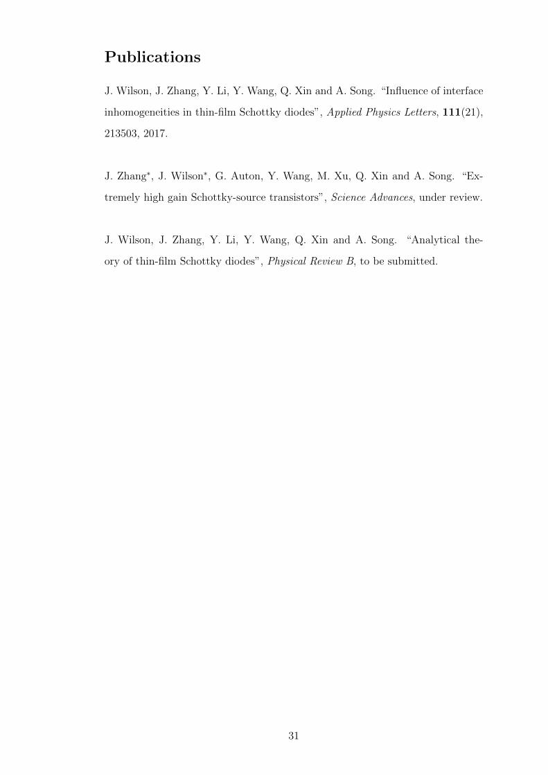
Publications
J. Wilson, J. Zhang, Y. Li, Y. Wang, Q. Xin and A. Song. “Influence of interface
inhomogeneities in thin-film Schottky diodes”, Applied Physics Letters, 111(21),
213503, 2017.
J. Zhang∗, J. Wilson∗, G. Auton, Y. Wang, M. Xu, Q. Xin and A. Song. “Ex-
tremely high gain Schottky-source transistors”, Science Advances, under review.
J. Wilson, J. Zhang, Y. Li, Y. Wang, Q. Xin and A. Song. “Analytical the-
ory of thin-film Schottky diodes”, Physical Review B, to be submitted.
31

1 Introduction
1.1 Background and Motivation
We are able to fit a phone, a camera, a bank, a music library, an actual library,
a shopping centre, the sum of all human knowledge, a television and most im-
portantly a torch, into a five inch long block that we carry around everywhere.
The development of the smartphone is one of many results of the technology
revolutions that have disrupted the way that we interact with the world. In-
deed, society has changed fundamentally since the first integrated circuits were
fabricated sixty years ago. However, the journey from the first integrated circuit
to modern electronics has relied heavily on the scalability of silicon transistors,
which is reaching its limits. Moreover, while the hegemony of conventional sili-
con will continue for some time, it is difficult to escape its requirement for a rigid
form factor. Thus, if technological progress is to continue unabated, the success
of silicon-based microelectronics must be used as a springboard for advances in
new materials and device structures.
Thin-film electronics offers the opportunity to move past some of the limita-
tions of silicon. As early as 1968 flexible thin-film transistors (TFTs) fabricated
by Westinghouse led a Popular Science article to claim, perhaps ambitiously,
that [1]:
“Someday soon you may be able to buy a pad of operating electronic circuits just
the way you now buy a pad of paper.”
While this vision of paper electronics is not yet fully realised, it brings into focus
the scale of the change that may be brought about by thin-film electronics; ev-
eryday objects transformed into “smart” objects. Indeed, it is predicted that by
2027, tens of billions of smart objects will be internet enabled [2] and the printed,
flexible and organic electronics market will be worth over $73 billion [3]. In order
to match these predictions, thin-film electronics must be brought to a maturity
comparable with traditional microelectronics. Such a goal can only be achieved
through a combination of developments in device physics, materials science and
fabrication techniques.
32

Currently, efforts to realise large-area flexible thin-film electronics incorporate
a large variety of materials and techniques [4–7]. Among these, oxide semicon-
ductors, particularly amorphous indium-gallium-zinc-oxide (IGZO), have demon-
strated excellent electrical and optical properties [8–11]. The wide bandgap of
oxide semiconductors (typically > 3 eV) allows for high optical transparency,
while room-temperature processability offers compatibility with flexible sub-
strates. Moreover, their performance and ease of implementation in comparison
to competing materials means that oxide semiconductors are leading candidates
for application [12–17].
The first flexible oxide semiconductor TFTs were fabricated by Nomura et
al. in 2004 [10]. Since then, most studies on oxide semiconductors have focussed
on TFTs [7, 18]. Successes include high mobility, high optical transparency, low
voltage operation as well as integration into circuits [10, 19–21]. However, there
remain major barriers to wider adoption. In display technology, which is a target
area for IGZO TFTs, sensitivity to negative bias illumination temperature stress
(NBITS) has made it difficult to incorporate IGZO without sufficient light shield-
ing measures [22–30]. Moreover, short-channel effects limit the potential for the
kind of device scaling that has served silicon technology so well. Currently, the
characteristics of IGZO TFTs degrade when the channel length is reduced below
5 µm [31–33].
In recent years, oxide semiconductor Schottky diodes have also started to re-
ceive attention [34–37]. Major steps have been taken towards developing diodes
that are viable for applications such as radio frequency identification, which may
be used in smart packaging. Foremost among these developments are demonstra-
tions of flexibility [34], gigahertz operating frequencies [37,38] and a combination
of the two [17]. Despite this early technical success, research is still in its infancy
and there remain dependencies of diode behaviour that defy explanation.
IGZO Schottky junctions have also found use in other thin-film device archi-
tectures and applications including metal-semiconductor field-effect transistors
(MESFETs) [39], memory storage [40, 41] and energy harvesting [42]. Investiga-
tions have also commenced into Schottky source transistors (SSTs), an innovative
33

form of TFT that uses a Schottky barrier at the source to modulate the current
in the channel. SSTs hold several interesting advantages over TFTs that make
them particularly attractive for large-area and wearable display applications. A
lower sensitivity to alignment issues offers the possibility of using less robust, and
therefore cheaper, deposition and patterning techniques. Fabrication costs may
also be lowered as the SST has a reduced dependence on the stability of the active
channel, which will enable the use of a wider range of semiconductor materials.
The flatter saturation of the SST output characteristics enable them to act as
excellent current sources, providing a stable current to pixels across a large area,
thus ensuring the homogeneous pixel intensity required for a high-quality image.
The SST characteristics also saturate at a lower voltage than a TFT, thereby
offering the potential for lower power consumption and a reduced dependence
upon bulky batteries which provide a significant barrier to the development of
wearable electronics. However, as several features of SST characteristics remain
unexplained, the operating mechanism must be fully understood before any at-
tempt at large-scale application can be made.
For thin-film electronics to really take-off it must be built on a firm under-
standing of device and material physics, just like standard microelectronics. How-
ever, thin-film electronic devices do not necessarily conform to the assumptions
that are made for silicon devices. In thin-film electronics there is a push towards
more cost effective fabrication techniques, such as printing and the use of dis-
ordered materials, such as IGZO and organic semiconductors. Together, these
factors lead to a greater incidence of imperfections in thin-film electronic devices,
particularly at interfaces between materials. Thus, there is a need to understand
the role that disorder plays in thin-film electronic devices.
This thesis focuses on Schottky junctions in thin-film electronic devices. Two
devices, the Schottky diode and the Schottky source transistor are considered.
Particular focus is given to the effects of disorder at the Schottky junction and
how this relates to the behaviour of fabricated devices.
34
1.2 Aims and Objectives
This thesis aims to develop a deeper understanding of Schottky junctions in
thin-film electronics, with a view to demonstrating high performance oxide semi-
conductor Schottky source transistors. The simplest device containing a Schot-
tky contact is the Schottky diode, yet these devices still exhibit some unusual
behaviour. In the literature, thin-film Schottky diodes have been shown to ex-
hibit a thickness dependence, but no explanation for this trend has ever been
proposed [17, 42–44]. Thus, in order to obtain a fuller understanding of device
behaviour, the origins of the thickness dependence should be established. An an-
alytical theory which captures the origins of this behaviour should be developed
to offer insights into device physics and aid device design. Particular attention
should be paid to inhomogeneous Schottky interfaces as the materials used for
thin-film electronics are often more disordered than conventional materials.
Once there is a clearer understanding of thin-film Schottky junctions, the
knowledge generated can be applied to the SST. Oxide semiconductor SSTs
present several technical and theoretical challenges. First and foremost, a method
should be established for forming reliable Schottky contacts on an oxide semicon-
ductor channel layer. Secondly, though SSTs have previously shown potential as
high gain devices, there is currently no theory describing how to tune, and thereby
maximise, the gain [45]. Detailed studies should be carried out to elucidate what
limits the gain and a method of control should be established. As current in
the SST is controlled by the Schottky source contact rather than the channel,
it is worth considering what other advantages the SST may have over TFTs.
For example, do issues like short channel effects and NBITS, which plague oxide
semiconductor TFTs, have a similar impact on SSTs? Further still, can other
materials, which are unsuitable for use in TFTs, be incorporated into SSTs? The
answers to such questions will have a strong bearing upon the applicability of the
SST device structure.
35
1.3 Thesis Structure
This thesis is made up of six chapters. Chapter 2 contains a literature review
of oxide semiconductors. The properties of these materials are discussed, with
particular attention paid to IGZO. The device physics, operating mechanisms and
applications of Schottky contacts, TFTs and SSTs are also introduced. Chapter 3
demonstrates a dependence of the current in thin-film Schottky diodes upon the
thickness of the semiconductor. Possible reasons for the thickness dependence
are discussed with respect to the reverse current and the origin is found to be
barrier height inhomogeneities. The effects of barrier height inhomogeneities
upon forward current are also discussed. Finally, the areal dependence of the
reverse current density is considered. In Chapter 4 an analytical theory of thin-
film Schottky diodes is devised and compared to the results of device simulations.
The theory is developed to incorporate barrier height inhomogeneities under a
variety of conditions. Chapter 5 starts by developing a method to produce a
Schottky junction on an oxide semiconductor by tuning sputtering power and
oxygen content. The effects of varying these conditions are demonstrated on
Schottky diodes and SSTs. A strong dependence of the SST drain current upon
semiconductor thickness is demonstrated and attributed to inhomogeneities in
source barrier height. The effects of inhomogeneities upon SST behaviour are
investigated with the aid of device simulations. SSTs are optimised and fitted
with an analytical theory. The optimised IGZO SSTs are shown to have record
gain, high stability under NBITS and are unaffected by the short-channel effect
down to 360 nm. Finally, SSTs with a quasi-metallic indium tin oxide channel
layer are demonstrated. Chapter 6 presents the conclusions of the thesis and the
future prospects of work in this area.
36

2 Background: Materials and Devices
2.1 Oxide Semiconductors
2.1.1 Introduction
The earliest known work on the electrical conductivity and optical transparency
of metal oxides was carried out on CdO in 1907 [46]. This was followed up
in 1937 by similar work on SnO2 [47]. Though investigations into transparent
conducting oxides (TCOs) continued [48–50], the first attempt to produce a thin-
film transistor (TFT) using an oxide semiconductor layer was not made until 1964
[51]. The work of Klasens, using n-type SnO2, was followed by the incorporation
of ZnO into the TFT structure in 1968 [52]. In the following years, work on
metal oxides as transparent conductors continued [53–55], with TCOs finding
applications as transparent electrodes, window heaters and gas sensors [49, 56–
58]. However, there was limited follow-up work on devices using metal oxides as
semiconductors due to the poor electrical characteristics they displayed [59].
The potential of oxide semiconductors only came to light in the mid-90s when
several major advances were made. In 1996 Hosono et al. hypothesised that
the oxides of heavy metal cations with an electron configuration of (n− 1)d10ns0
would be promising for use as TCOs [8]. These metal cations have become useful
in the design of amorphous oxide semiconductors for several reasons. Firstly, the
conduction band minimum comprises large spherical s-orbitals, resulting in high
electron mobility and insensitivity to structural randomness. Secondly, they have
a wide bandgap allowing for optical transparency.
The possibility of transparent electronics using oxide semiconductors became
apparent in the same year when Prins et al. fabricated TFTs with an SnO2
channel layer [60]. These devices had an on/off ratio of only 60 and optical ab-
sorption was “tens of percent” due to the choice of SrRuO3 as the gate electrode.
In 1997, Kawazoe et al. demonstrated the first transparent p-type metal oxide,
CuAlO2 [61], paving the way for future complementary circuits.
37
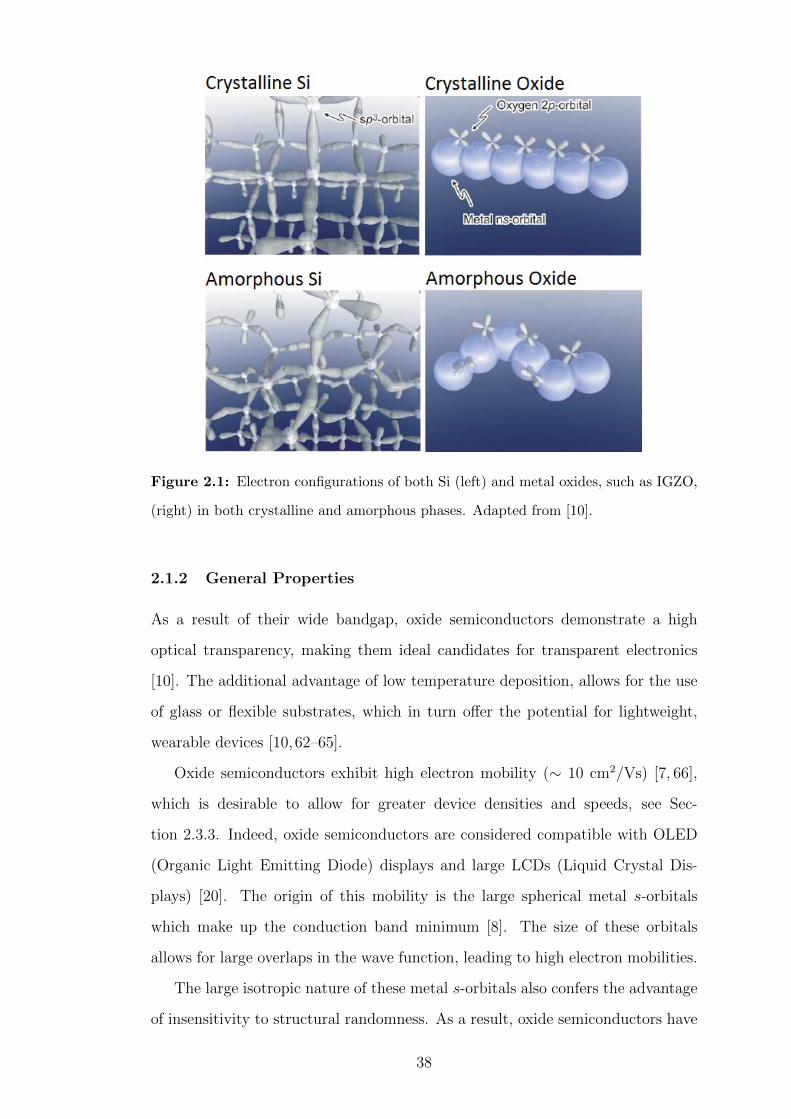
Figure 2.1: Electron configurations of both Si (left) and metal oxides, such as IGZO,
(right) in both crystalline and amorphous phases. Adapted from [10].
2.1.2 General Properties
As a result of their wide bandgap, oxide semiconductors demonstrate a high
optical transparency, making them ideal candidates for transparent electronics
[10]. The additional advantage of low temperature deposition, allows for the use
of glass or flexible substrates, which in turn offer the potential for lightweight,
wearable devices [10, 62–65].
Oxide semiconductors exhibit high electron mobility (∼ 10 cm2/Vs) [7, 66],
which is desirable to allow for greater device densities and speeds, see Sec-
tion 2.3.3. Indeed, oxide semiconductors are considered compatible with OLED
(Organic Light Emitting Diode) displays and large LCDs (Liquid Crystal Dis-
plays) [20]. The origin of this mobility is the large spherical metal s-orbitals
which make up the conduction band minimum [8]. The size of these orbitals
allows for large overlaps in the wave function, leading to high electron mobilities.
The large isotropic nature of these metal s-orbitals also confers the advantage
of insensitivity to structural randomness. As a result, oxide semiconductors have
38

a major advantage over other amorphous semiconductors such as hydrogenated
amorphous silicon (a-Si:H) and organic semiconductors such as pentacene (which
have comparatively low mobilities [6]). In Si the conduction band minimum
is made up of hybridised sp3-orbitals, as illustrated in Fig. 2.1. The overlaps
between these orbitals are small, making them very sensitive to bond angle fluc-
tuations caused by structural randomness. Hence, in a-Si:H, which has almost
complete structural randomness, the sp3-orbitals overlap less than in crystalline
Si. This produces deeper tail states below the conduction band minimum where
carriers will be trapped, causing carrier transport to occur by hopping between
localised tail states and not by band conduction [10]. Disordered organic semi-
conductors suffer from a similar problem. Most carrier transport occurs via hop-
ping conduction and carriers are scattered each time they move between localised
states [6]. Such issues lead to a reduction in mobility, which hinders commercial
application, as future products will require higher speeds and smaller sizes [67,68].
Tail states may also increase the off-current in TFTs as they effectively reduce
the bandgap.
An amorphous microstructure does not affect metal oxides of heavy metal
cations as the overlap between the spherical s-orbitals of neighbouring metal
atoms is so large that they are insensitive to structural distortions, as shown in
Fig. 2.1. In these metal oxides, band conduction persists even in the amorphous
state, hence the high mobilities achieved in the crystalline structure are more
easily retained [8]. Furthermore, the amorphous structure allows oxide semicon-
ductors to demonstrate uniformity over large areas [10].
For all the promise that metal oxides show as n-type semiconductors, there is a
notable dearth of success as p-type semiconductors. P -type oxide semiconductors
have low hole mobility [69–71], causing them to fall short of the requirements for
practical application [18, 66]. Their low mobility is attributed to the localized
O 2p orbitals that dominate the valence band maximum, giving rise to hopping
conduction [72]. One material showing some promise is SnO, in which the top
of the valence band consists of hybridised Sn 5s and O 2p orbitals. Sn 5s states
contributing to valence band maximum can potentially lead to sufficient hole
39

mobility without high processing temperatures [7,73]. Indeed, when incorporated
into TFTs, SnO has displayed mobility > 1 cm2/Vs and on/off ratios as high as
106 [74–76].
In all, oxide semiconductors compare favourably to competing materials for
thin-film electronics such as a-Si:H, polysilicon and organics.
2.1.3 Zinc Oxide (ZnO)
Zinc oxide is a highly versatile material that has already found myriad applica-
tions including rubber vulcanisation, wound treatment and electronic devices [77].
ZnO is an n-type semiconductor, largely used in poly-crystalline form; its 3.4 eV
bandgap makes it transparent in the visible spectrum [78]. The first notable work
on ZnO as a semiconductor was reported in 1968 when Boesen and Jacobs fab-
ricated a TFT with a Li doped ZnO single crystal channel layer [52]. The drain
current (ID) of the TFT was low and the device had limited dependence on gate
voltage (VG). Following these reports, interest in the use of ZnO for an active
channel region dwindled.
However, interest was revived in 2003 when Hoffman et al., Carcia et al.
and Masuda et al. all produced TFTs with ZnO active layers. Hoffman et al.
fabricated ZnO TFTs with a transparency of ∼ 75% in the visible spectrum, an
on/off ratio of 107 and electron mobilities (see Section 2.3.3) from 0.3−2.5 cm2/Vs
[79]. The ZnO active regions were deposited on to glass substrates by ion beam
sputtering, but the fabrication method required high processing temperatures
(600 – 800 °C).
Carcia et al. deposited ZnO onto Si substrates via radio frequency (RF)
magnetron sputtering, an important step as this deposition method is conducive
to room temperature processing [80]. The resulting TFTs had on/off ratios > 106
and electron mobilities of 2 cm2/Vs, comparable with the work of Hoffman et al..
The ZnO films had a transparency > 80% in the visible spectrum, but the devices
themselves were not transparent.
Masuda et al. deposited ZnO using pulsed laser deposition (PLD) at 450 °C,
achieving transparency > 80% in the visible spectrum for TFTs on glass sub-
40
strates [81]. However, the electrical performance of the devices was comparatively
poor. In subsequent years there has been a concerted effort to improve the quality
of ZnO TFTs and the ease with which they can be fabricated. These include,
but are by no means limited to:
Improvements in mobility, including mobility consistently higher than
50 cm2/Vs in RF sputtered polycrystalline ZnO TFTs [82–86].
Implementation of solution processes [87–90].
Simulations to elucidate factors affecting electrical behaviour [91].
Incorporation of dopants to improve electrical characteristics [89,90,92].
In spite of these efforts, and more, there remain some major question marks over
the suitability of ZnO for application in transparent electronics. The principle
limitation is the grain boundaries present in the polycrystalline structure obtained
when depositing ZnO thin-films [79, 91]. Potential barriers are formed at these
sites, scattering carriers. Moreover, for small grain sizes the depletion regions
in the crystals could overlap, causing further scattering and inducing a higher
resistivity [7, 91]. These factors contribute to limiting the carrier mobility and
inhomogeneous performance over large areas; both are major obstacles to prac-
tical application. Moreover, a poor durability in both acid etchants and reduced
atmospheres makes fabrication more complicated [18]. These issues with ZnO
and other polycrystalline oxide semiconductors have caused research interest to
shift towards amorphous materials, specifically IGZO.
2.1.4 Indium Gallium Zinc Oxide (IGZO)
The first indium gallium zinc oxide TFTs were fabricated by Nomura et al. in
2003 [9]. PLD was used to deposit a 2 nm ZnO layer onto the yttria-stabilised
zirconia substrate, followed by a 120 nm single crystalline InGaO3(ZnO)5 layer.
The TFTs exhibited excellent electrical properties, including a field-effect mobil-
ity of 80 cm2/Vs, an on voltage (VON , see Section 2.3.3) of −0.5 V and an on/off
ratio of 106. Transparency > 80% in the visible spectrum further confirmed the
41
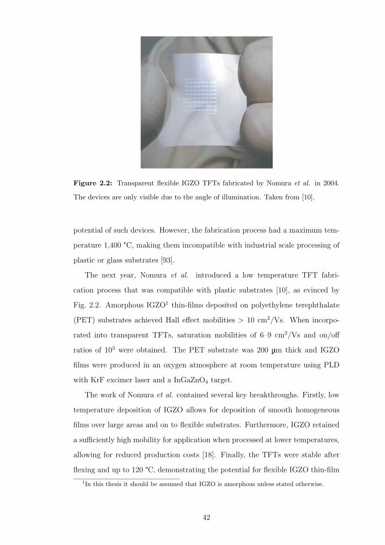
Figure 2.2: Transparent flexible IGZO TFTs fabricated by Nomura et al. in 2004.
The devices are only visible due to the angle of illumination. Taken from [10].
potential of such devices. However, the fabrication process had a maximum tem-
perature 1,400 °C, making them incompatible with industrial scale processing of
plastic or glass substrates [93].
The next year, Nomura et al. introduced a low temperature TFT fabri-
cation process that was compatible with plastic substrates [10], as evinced by
Fig. 2.2. Amorphous IGZO1 thin-films deposited on polyethylene terephthalate
(PET) substrates achieved Hall effect mobilities > 10 cm2/Vs. When incorpo-
rated into transparent TFTs, saturation mobilities of 6–9 cm2/Vs and on/off
ratios of 103 were obtained. The PET substrate was 200 µm thick and IGZO
films were produced in an oxygen atmosphere at room temperature using PLD
with KrF excimer laser and a InGaZnO4 target.
The work of Nomura et al. contained several key breakthroughs. Firstly, low
temperature deposition of IGZO allows for deposition of smooth homogeneous
films over large areas and on to flexible substrates. Furthermore, IGZO retained
a sufficiently high mobility for application when processed at lower temperatures,
allowing for reduced production costs [18]. Finally, the TFTs were stable after
flexing and up to 120 °C, demonstrating the potential for flexible IGZO thin-film
1In this thesis it should be assumed that IGZO is amorphous unless stated otherwise.
42

Pro
pert
ya-S
i:H
LT
PS
Penta
cen
eIG
ZO
Mob
ilit
y(c
m2/V
s)≤
150
-100
0.1-
101-
100
Man
ufa
cturi
ng
Cos
tL
owH
igh
Low
Low
Rel
iabilit
yL
owH
igh
Low
inai
rH
igh
Yie
ldH
igh
Med
ium
Hig
hH
igh
Pro
cess
Tem
per
ature
(°C
)∼
250
≤50
0R
oom
Tem
p.
Room
Tem
p.
-35
0
Mic
rost
ruct
ure
Am
orphou
sP
olycr
yst
alline
Pol
ycr
yst
alline
Am
orphou
s
Dev
ice
Typ
eN
MO
SC
MO
SP
MO
SN
MO
S
Pro
cess
Com
ple
xit
yL
owH
igh
Ver
yL
owL
ow
Ban
dga
p(e
V)
1.6
1.1
1-
2≥
3
Min
imum
TF
TSta
ndby
Pow
er(W
)∼
10−
12
>10−
12
∼10−
12
<10−
13
Table
2.1:
Pro
per
ties
ofIG
ZO
com
par
edto
com
pet
ing
typ
esof
sem
icon
du
ctor
[6,7
,66–68,9
4–99].
43

electronics.
As a result of further optimisation, IGZO is now established as the foremost
oxide semiconductor and has many advantages over competing materials, see
Table 2.1. To understand why IGZO has such good performance, the roles of
the individual cations and the disadvantages of alternative binary and ternary
compounds must be understood. The advantages and disadvantages of ZnO have
been outlined in greater detail in Section 2.1.3. Another binary compound, In2O3,
has high carrier concentrations (∼ 1018 cm−3), which pushes the Fermi level (EF )
very close to or even above the conduction band minimum. This makes it difficult
to create off-states in any devices [7]. Furthermore, as In2O3 is polycrystalline
it still suffers with the problem of grain boundaries [66]. Using two or more
cations with different ionic charges and sizes can suppress crystallisation and
produce amorphous films. In In-based semiconductors, Ga and Zn can help to
frustrate crystallization [100], resolving the issue of grain boundaries. For ex-
ample, ZnO and In2O3 produce crystalline films even when deposited at room
temperature [66], however, indium zinc oxide (IZO) can easily be deposited in
the amorphous phase. Nevertheless, IZO has issues with light sensitivity [101],
bias stress stability [102] and very high carrier densities [7,103]. Suppressing car-
rier generation, so that the carrier concentration can be controlled by the gate
bias, is the main issue facing the use of IZO in TFTs. Incorporation of triva-
lent or tetravalent elements such as Ga3+ [10], Si4+ [102, 104], Hf4+ [105] and
Zr4+ [106] can suppress and/or stabilise the carrier generation. This suppression
occurs because these ions form stronger bonds with oxygen than In or Zn ions,
reducing the number of oxygen vacancies that act as electron donors in metal ox-
ides [68,102,107,108]. Of these elements, Ga is currently the electron suppressor
of choice [7, 68]. Ga2O3 alone has a very large resistivity (108 Ωcm), contributed
to by very low carrier concentration, a large density of empty traps and a large
bandgap (in the region of 4.84–5.04 eV for direct transition) [7, 109].
The ratios of ZnO, In2O3 and Ga2O3 used to form IGZO have been studied
in detail [7, 110]. Figure 2.3 gives an example of how composition can affect the
electrical properties of IGZO TFTs. Due to the large bandgap energy of Ga2O3,
44
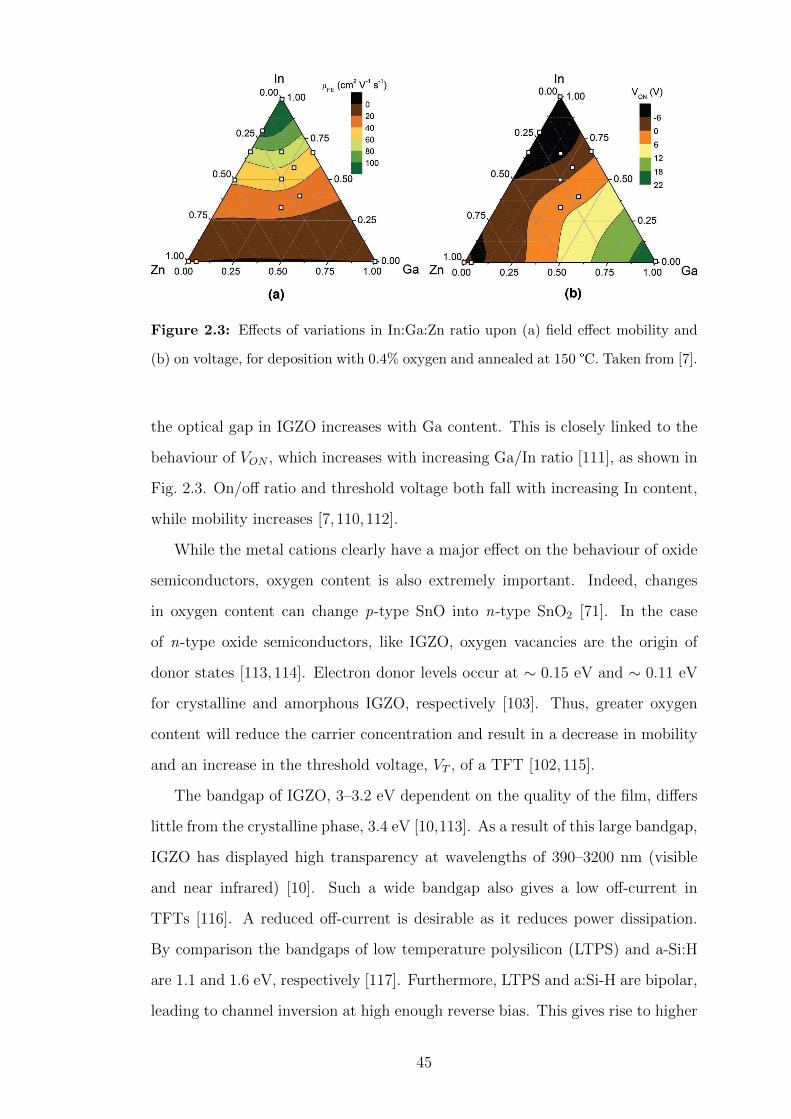
Figure 2.3: Effects of variations in In:Ga:Zn ratio upon (a) field effect mobility and
(b) on voltage, for deposition with 0.4% oxygen and annealed at 150 °C. Taken from [7].
the optical gap in IGZO increases with Ga content. This is closely linked to the
behaviour of VON , which increases with increasing Ga/In ratio [111], as shown in
Fig. 2.3. On/off ratio and threshold voltage both fall with increasing In content,
while mobility increases [7, 110,112].
While the metal cations clearly have a major effect on the behaviour of oxide
semiconductors, oxygen content is also extremely important. Indeed, changes
in oxygen content can change p-type SnO into n-type SnO2 [71]. In the case
of n-type oxide semiconductors, like IGZO, oxygen vacancies are the origin of
donor states [113, 114]. Electron donor levels occur at ∼ 0.15 eV and ∼ 0.11 eV
for crystalline and amorphous IGZO, respectively [103]. Thus, greater oxygen
content will reduce the carrier concentration and result in a decrease in mobility
and an increase in the threshold voltage, VT , of a TFT [102,115].
The bandgap of IGZO, 3–3.2 eV dependent on the quality of the film, differs
little from the crystalline phase, 3.4 eV [10,113]. As a result of this large bandgap,
IGZO has displayed high transparency at wavelengths of 390–3200 nm (visible
and near infrared) [10]. Such a wide bandgap also gives a low off-current in
TFTs [116]. A reduced off-current is desirable as it reduces power dissipation.
By comparison the bandgaps of low temperature polysilicon (LTPS) and a-Si:H
are 1.1 and 1.6 eV, respectively [117]. Furthermore, LTPS and a:Si-H are bipolar,
leading to channel inversion at high enough reverse bias. This gives rise to higher
45
off-currents and greater power dissipation.
For the reasons discussed above and in Table 2.1, as well as inadequate p-
type transistors [118], instability under illumination [94] and electrical bias stress
[95], the display industry will probably transition away from a-Si:H in the near
future. Prior to the adoption of any successor material, the ease of processing
said material must also be considered. Organic semiconductors do offer excellent
processing options, including spin-coating and printing. However, the technology
is not sufficiently mature and they remain limited by low mobility and poor air
stability [6, 97, 98].
While it has a high mobility and a favourable deposition temperature [96],
LTPS requires more complex processing than IGZO [68]. This makes up for the
slightly lower mobility of IGZO, which can probably be improved in the future
by different cation choices and tuning cation ratios in the oxide semiconductor
system.
In addition to the processing itself, the associated expense of transitioning
fabrication facilities from one material to another may also be prohibitive. The
processing for IGZO is likely compatible with a-Si:H, meaning that machines can
be retrofitted and the transition cost will be lower. By comparison, processing
LTPS may require expensive new fabrication facilities [68].
The electron affinity (χSC) of IGZO is 4.16 eV [119]. This electron affinity
means that ohmic contacts are readily made between IGZO and a multitude of
metals including Al and Ti [120,121]. However, formation of good Schottky con-
tacts is heavily dependent upon the inclusion of oxygen [34,122]; see Section 2.2.7.
Another major advantage of IGZO is the absence of grain boundaries, leading
to electrical characteristics that are homogeneous over large areas. This makes
IGZO far more compatible with large-area display applications. However, in
IGZO a new limitation is introduced by the random distribution of Ga3+ and
Zn2+ ions [103]. The random distribution of cations leads to a landscape of po-
tential barriers near the conduction band minimum. Carriers with more energy
will be able to take shorter paths through the potential landscape than the car-
riers with lower energy, as shown in Fig. 2.4. As a consequence, mobility will
46
Figure 2.4: Percolation conduction over a spatially varying random distribution of
potential barriers in the conduction band minimum. Electron (a) has greater energy,
taking a higher shorter path than electron (b). Adapted from [103].
increase with temperature (up to a point) and free electron density. In most
crystalline semiconductors, increasing temperature causes greater scattering by
lattice vibrations and increasing free electron density leads to greater scattering
off ionised donors and acceptors, both of which reduce mobility.
An issue that does still pose a problem for IGZO application is negative bias
illumination stress. When IGZO TFTs are held at negative bias under illumina-
tion of near bandgap energy photons, there is a large negative shift in VT [22–24].
Such instability makes it impractical to incorporate IGZO into displays.
Another issue that needs to be addressed is the fact that Ga and In are
expensive: $400/kg and $340/kg respectively, compared to Zn and Si, both
∼ $2/kg [123]. Ideally, devices would be made with the cheapest, most abundant
materials, which is why attempts have been made to remove In from devices [124].
However, as things stand, metal oxides remain heavily reliant on expensive raw
materials.
2.2 Schottky Contacts
2.2.1 Introduction
Metal-semiconductor contacts are one of the pillars of modern electronics. These
junctions can be split into two groups, ohmic and Schottky contacts. Ohmic
47

contacts allow for the passage of current in proportion to the applied voltage
and with a magnitude which is independent of direction. By contrast, Schottky
contacts display rectifying behaviour, passing current in one direction far more
easily than the other. Schottky contacts are fundamental to the operation of
many devices, including the Schottky diode and the MESFET, and have proven
useful for a host of applications, from signal rectification to energy storage.
The study of metal-semiconductor contact rectification goes back as far as
Munck af Rosenschold in 1835 and Braun in 1874 [125,126]. Though diodes with
different metal contacts were useful in early radio work, there was little theoretical
understanding of their behaviour until the 1930s [127, 128]. In 1938, Schottky
and Mott independently observed that the rectification was due to charge carriers
passing over a potential barrier via drift diffusion [129,130]. In the first established
theory, Schottky, building upon the work of Mott, modelled a parabola-shape
barrier, which is why the Schottky diode bears his name [131]. Since the work
of Bethe in 1942, it has been understood that thermionic emission, rather than
diffusion, is the current limiting mechanism in Schottky contacts on Si [132]. Since
this time, the development in understanding of metal-semiconductor contacts has
been well documented in literature [133–136].
2.2.2 Depletion Approximation
When a semiconductor and a metal are brought together their Fermi levels will
align, causing bands in the semiconductor to bend and create a potential barrier
known as a Schottky barrier. For n-type semiconductors the Schottky barrier
height (the energy ΦB in eV or the potential φB in V) is the difference between
the conduction band minimum, EC , and EF at the interface, whereas for p-
type semiconductors the Schottky barrier is the difference between EF and the
valence band maximum, EV . As this thesis is focused on oxide semiconductors,
particularly n-type IGZO, this section will focus on the n-type case where the
metal work function, ΦM > ΦSC , the work function of the semiconductor.
In this case, the bands in the semiconductor bend upwards near the interface
with the metal and a depletion region of width WD forms, as shown in Fig. 2.5.
48
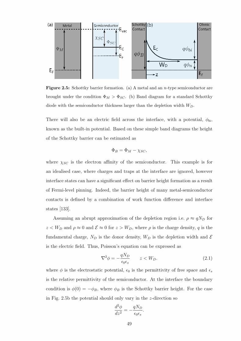
Figure 2.5: Schottky barrier formation. (a) A metal and an n-type semiconductor are
brought under the condition ΦM > ΦSC . (b) Band diagram for a standard Schottky
diode with the semiconductor thickness larger than the depletion width WD.
There will also be an electric field across the interface, with a potential, φbi,
known as the built-in potential. Based on these simple band diagrams the height
of the Schottky barrier can be estimated as
ΦB = ΦM − χSC ,
where χSC is the electron affinity of the semiconductor. This example is for
an idealised case, where charges and traps at the interface are ignored, however
interface states can have a significant effect on barrier height formation as a result
of Fermi-level pinning. Indeed, the barrier height of many metal-semiconductor
contacts is defined by a combination of work function difference and interface
states [133].
Assuming an abrupt approximation of the depletion region i.e. ρ ≈ qND for
z < WD and ρ ≈ 0 and E ≈ 0 for z > WD, where ρ is the charge density, q is the
fundamental charge, ND is the donor density, WD is the depletion width and E
is the electric field. Thus, Poisson’s equation can be expressed as
∇2φ = −qND
ε0εsz < WD. (2.1)
where φ is the electrostatic potential, ε0 is the permittivity of free space and εs
is the relative permittivity of the semiconductor. At the interface the boundary
condition is φ(0) = −φB, where φB is the Schottky barrier height. For the case
in Fig. 2.5b the potential should only vary in the z-direction so
d2φ
dz2= −qND
ε0εs.
49

Given that
E = −dφdz
=qND
ε0εsz + a
where a is a constant and using the boundary condition at z = WD,
dφ
dz=qND
ε0εs
(WD − z
).
Therefore, from the boundary condition at the interface
φ(z) = −φB +qND
ε0εs
(WD −
z
2
)z
and as EC(z) = −qφ(z)
EC(z) = qφB −q2ND
ε0εs
(WD −
z
2
)z. (2.2)
Given that E =1
q
dEcdz
E(z) = −qND
ε0εs(WD − z)
and
|E(z)| = qND
ε0εs(WD − z).
Thus,
WD =
√2ε0εsqND
(φbi − V −
kT
q
)(2.3)
and
|E(0)| = EM =qND
ε0εsWD =
√2qND
ε0εs
(φbi − V −
kT
q
)(2.4)
where k is the Boltzmann constant, T is the temperature, V is the applied voltage
and EM is the maximum electric field in the semiconductor, which occurs at the
interface. The kT/q term in Eq. 2.3 is the contribution of the electron density to
the right-hand side of Eq. 2.1, see [133]. Thus, the capacitance per unit area of
the depletion layer can be obtained using CD = ε0εs/WD, leading to the following
relationship between CD and the applied voltage:
C−2D =
2(φbi − V − kT
q
)qεsND
. (2.5)
Figure 2.6 compares the depletion approximation with the results of device
simulations carried out using Silvaco Atlas. A Schottky diode structure was
50
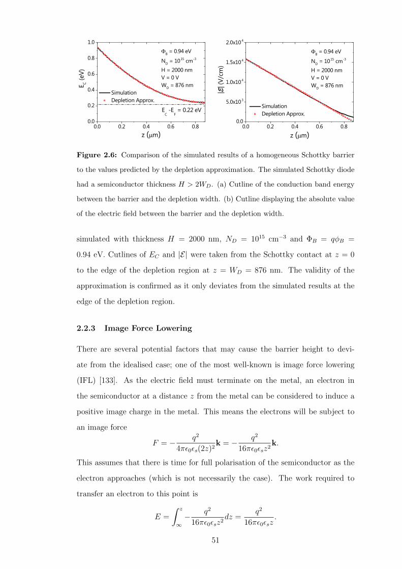
0.0 0.2 0.4 0.6 0.80.0
0.2
0.4
0.6
0.8
1.0
0.0 0.2 0.4 0.6 0.80.0
5.0x10 3
1.0x10 4
1.5x10 4
2.0x10 4
E C (e
V)
z ( m)
EC -E
F = 0.22 eV
Simulation Depletion Approx.
B = 0.94 eV
ND = 1015 cm-3
H = 2000 nmV = 0 VW
D = 876 nm
|E| (
V/c
m)
z ( m)
B = 0.94 eV
ND = 1015 cm-3
H = 2000 nmV = 0 VW
D = 876 nm
Simulation Depletion Approx.
Figure 2.6: Comparison of the simulated results of a homogeneous Schottky barrier
to the values predicted by the depletion approximation. The simulated Schottky diode
had a semiconductor thickness H > 2WD. (a) Cutline of the conduction band energy
between the barrier and the depletion width. (b) Cutline displaying the absolute value
of the electric field between the barrier and the depletion width.
simulated with thickness H = 2000 nm, ND = 1015 cm−3 and ΦB = qφB =
0.94 eV. Cutlines of EC and |E| were taken from the Schottky contact at z = 0
to the edge of the depletion region at z = WD = 876 nm. The validity of the
approximation is confirmed as it only deviates from the simulated results at the
edge of the depletion region.
2.2.3 Image Force Lowering
There are several potential factors that may cause the barrier height to devi-
ate from the idealised case; one of the most well-known is image force lowering
(IFL) [133]. As the electric field must terminate on the metal, an electron in
the semiconductor at a distance z from the metal can be considered to induce a
positive image charge in the metal. This means the electrons will be subject to
an image force
F = − q2
4πε0εs(2z)2k = − q2
16πε0εsz2k.
This assumes that there is time for full polarisation of the semiconductor as the
electron approaches (which is not necessarily the case). The work required to
transfer an electron to this point is
E =
∫ z
∞− q2
16πε0εsz2dz =
q2
16πε0εsz.
51
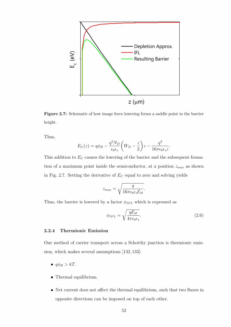
E C (e
V)
z ( m)
Depletion Approx. IFL Resulting Barrier
Figure 2.7: Schematic of how image force lowering forms a saddle point in the barrier
height.
Thus,
EC(z) = qφB −q2ND
ε0εs
(WD −
z
2
)z − q2
16πε0εsz.
This addition to EC causes the lowering of the barrier and the subsequent forma-
tion of a maximum point inside the semiconductor, at a position zmax as shown
in Fig. 2.7. Setting the derivative of EC equal to zero and solving yields
zmax =
√q
16πε0εsEM.
Thus, the barrier is lowered by a factor φIFL which is expressed as
φIFL =
√qEM
4πε0εs. (2.6)
2.2.4 Thermionic Emission
One method of carrier transport across a Schottky junction is thermionic emis-
sion, which makes several assumptions [132,133]:
qφB > kT .
Thermal equilibrium.
Net current does not affect the thermal equilibrium, such that two fluxes in
opposite directions can be imposed on top of each other.
52
In thermionic emission theory only electrons with energies greater than the barrier
height will contribute to the current and as such they are considered separately
from all other charge carriers and given their own quasi-Fermi level, EFn. As the
current is driven by the gradient of the quasi-Fermi level [134]
J = qµnne∇EFn
where J is the current density, µn is the mobility of the electrons and ne is
the density of electrons. It is assumed that EFn is flat in the depletion region,
equivalent to assuming that the mobility of the semiconductor is infinite, making
the contribution of drift-diffusion negligible. This means that the only change in
EFn occurs at the interface, allowing the barrier height to be the only current
limiting mechanism. This assumption of infinite mobility means that thermionic
emission theory is best suited to explaining carrier transport in high mobility
semiconductors such as crystalline Si.
As the current from the semiconductor to the metal is made up entirely of con-
tributions from electrons with energy greater than the barrier height EFn + qφB:
Js→m =
∫ ∞EFn+qφB
qvzdne (2.7)
where vz is the velocity of electrons perpendicular to the barrier. Given that ne is
the product of the density of states, N(E), and the distribution function, F (E),
(in this case Boltzmann)
dne = N(E)F (E)dE
≈ 4π(2m∗)3/2
h3
√E − EC exp
(− E − EC + qφn
kT
)dE
where m∗ is the effective mass of the electron, h is the Planck constant, E is the
energy of the electron and φn is the Fermi potential from the conduction band
edge, i.e. −(EC −EF )/q. Assuming all of the energy of the charge carriers in the
conduction band is kinetic, such that
E − EC =1
2m∗v2
and
dE = m∗vdv,
53

-1.00 -0.50 0.00 0.50 1.0010-6
10-5
10-4
10-3
10-2
10-1
100
101
102
-2.0 -1.0 0.0 1.0 2.0
0
1x10¹³
2x10¹³
3x10¹³ (b)
B and n extraction
|J| (A
cm
-2)
V (V)
(a)
C-2
(cm
4 F-2
)
V (V)
ND extraction
Figure 2.8: Schottky diode characteristics. (a) How to extract ΦB and n from |J |-V
characteristics. (b) How to extract ND from C−2-V characteristics.
where v is the electron velocity, gives
dne ≈ 2
(m∗
h
)3
exp
(− qφnkT
)exp
(− m∗v2
2kT
)× 4πv2dv.
Substituting into Eq. 2.7 gives
Js→m ≈ 2q
(m∗
h
)3
exp
(− qφnkT
)∫ ∞v0x
exp
(− m∗v2
x
2kT
)dvx
×∫ ∞v0y
exp
(−m∗v2
y
2kT
)dvy
∫ ∞v0z
vz exp
(− m∗v2
z
2kT
)dvz
≈ 4πqm∗k2
h3exp
(− qφnkT
)exp
(− m∗v2
0z
2kT
)where v0z is the velocity required to overcome the barrier i.e.
q(φbi − V ) =m∗v2
0z
2.
Thus
Js→m = A∗T 2 exp
(− qφB
kT
)exp
(qV
kT
)where A∗ = 4πqm∗k2
h3is the Richardson constant. In the opposite direction the
current over the barrier is independent of the applied voltage and is equal to the
current when V = 0 to maintain thermal equilibrium, thus
J = A∗T 2 exp
(− qφB
kT
)[exp
(qV
kT
)− 1
]. (2.8)
The extent to which the diode adheres to this ideal equation can be reflected by
the ideality factor n, which is inserted into the equation to give
J = A∗T 2 exp
(− qφB
kT
)[exp
(qV
nkT
)− 1
].
54

-1.0 -0.5 0.0 0.5 1.010-10
10-9
10-8
10-7
10-6
10-5
10-4
10-3
10-2
10-1
100
101
-1.0 -0.5 0.0
2x10⁻¹⁰
4x10⁻¹⁰
6x10-108x10-10
10-9
|J| (
A c
m-2
)
V (V) ND = 1015 cm-3
B = 0.94 eV
n = 106 cm2 V-1 s-1
Simulated Theory
|J| (
A c
m-2
)
V (V)
Figure 2.9: |J |-V characteristics for thermionic emission theory and a simulated diode
with µ = 106 cm2/Vs. Such a large semiconductor mobility must be used as the theory
assumes an infinite mobility.
The values for φB and n can be extracted from the forward current of the J-V
curve, as shown in Fig. 2.8a. The free electron density could also be extracted
from the forward current of the J-V curve when it is in the series resistance
limited regime. However, the free electron concentration is dependent on the
trap density so it is more common to extract ND from the C−2-V curve using
Eq. 2.5, as shown in Fig. 2.8b. A comparison between thermionic emission theory
and a diode |J |-V curve simulated using Silvaco Atlas is shown in Fig. 2.9. The
larger the mobility used in the simulation, the greater the accuracy of the theory.
2.2.5 Diffusion Theory
Diffusion acts in series with thermionic emission and their relative contributions
to the current can be ascertained by considering thermionic emission diffusion
theory (a full discussion is beyond the scope of this thesis) [133,134,137]. While
thermionic emission is a good model for crystalline Si, as mobility is reduced
diffusion becomes the limiting factor in current transport, thus for disordered
materials, such as oxide semiconductors and organics, diffusion current must be
55

considered. Though widely known as the diffusion equation, drift is also incor-
porated so that the current is expressed as
Jz = q
(neµnE +Dn
dnedz
)where Jz is the current density in the z-direction and Dn = kT
qµn is the Einstein
relation. The first term in the equation describes drift (Ohm’s law), while the
second term describes diffusion (Fick’s law). Using the fact that E =1
q
dEcdz
:
Jz = qDn
(nekT
dEcdz
+dnedz
)by integrating both sides over the depletion region and using Ec(z)
kTas an integrat-
ing factor yields∫ WD
0
Jz exp
(Ec(z)
kT
)dz =
∫ WD
0
qDn exp
(Ec(z)
kT
)(nekT
dEcdz
+dnedz
)dz
=
∫ WD
0
qDnd
dz
[exp
(Ec(z)
kT
)ne(z)
]dz
=
∣∣∣∣WD
0
qDn
[exp
(Ec(z)
kT
)ne(z)
](2.9)
Given that the following boundary conditions apply:
EC(z) =
qφB z = 0
q(φn + V ) z = WD
and
ne(z) =
NC exp
(− Ec(0)− EFn(0)
kT
)= NC exp
(− qφB
kT
)z = 0
ND = NC exp
(− qφnkT
)z = WD
where NC is the effective density of states in the conduction band and the problem
is one-dimensional, so J(z) is independent of z:
Jz =
qDnNC exp
[exp
(qV
kT
)− 1
]∫WD
0exp
(Ec(z)
kT
)dz
(2.10)
For the standard depletion approximation the profile of the conduction band
minimum is given by
Ec(z) = qφBn −q2ND
ε0εs
(WDz −
z2
2
)56

Figure 2.10: Metal work function dependence upon crystal orientation for copper,
from [139]. Topography (a) and work function (b) were obtained using Kelvin probe
force microscopy. In (b) H, M and L stand for high, medium and low work function
respectively. The crystal orientation (c) was obtained using electron back scattered
diffraction.
therefore
Jz =
qDnNC exp
(− qφB
kT
)[exp
(qV
kT
)− 1
]∫WD
0exp
[− q2ND
ε0εskT
(WDz −
z2
2
)]dz
Rearranging so that
a2
(z2
2−WDz
)= a2(z −WD)2 − a2W 2
D
where a2 =q2ND
2ε0εskTand setting y = a(z −WD) gives
∫ WD
0
exp
[− q2ND
ε0εskT
(WDz −
z2
2
)]dz = a−1 exp(−a2W 2
D)
∫ aWD
0
exp(y2)dy
≈ 1
2a2WD
≈ 1
qkT
√2qND
ε0εs(φbi − V − kT
q)
This is Dawson’s integral and can be approximated like this because aWD > 2
[134,138]. Thus, using Eq. 2.4
Jz ≈ qµnNCEM exp
(− qφB
kT
)[exp
(qV
kT
)− 1
](2.11)
2.2.6 Barrier Height Inhomogeneities
Thus far it has been assumed that the barrier height at a metal-semiconductor
junction is homogeneous, but this is not the case in reality. There is evidence of
barrier height inhomogeneities in devices made with many materials, for example,
57

Si [140], GaN [141], diamond [142] and ZnO [143]. In fact barrier heights have
been shown to vary by hundreds of meV [144,145]. The origins of inhomogeneous
barrier height include the use of polycrystalline metal contacts, leading to spatial
variations in the metal work function, as shown in Fig. 2.10 [139, 146, 147]. The
use of disordered semiconductors and the presence of dangling bonds and other
irregularities at the Schottky interface will also contribute to the spatial variation
of the barrier height.
Despite over 100 years of research on metal-semiconductor junctions, the first
attempts to understand inhomogeneities were not made until the 1990s. While
theories of regions of different barrier heights conducting in parallel were pro-
posed, they failed to capture the reality of the physics [140]. The work of Tung
and Sullivan deals with the issue of inhomogeneities more accurately [148–150].
They demonstrated that saddle points in the potential can be formed under low
barrier regions. This does not require complex physics to understand, it is simply
a case of the potential from higher barrier regions (HBRs) enveloping lower bar-
rier regions (LBRs). If the Schottky barrier height varies across different regions
then:
φ(x, y, 0) = −φB(x, y) = −[φ0B − ψ(x, y)]
where ψ is the difference between the mean Schottky barrier height, φ0B, and the
local Schottky barrier height. Tung treated this perturbation as the potential due
to a dipole layer, φd, with a dipole moment per unit area of pA = 2ε0εsψ(x, y)k
[150].
φd(x, y, z) =1
4πε0εs
p · (r− r′)
|r− r′|3
=
∫S
1
4πε0εs
pA · (r− r′)
|r− r′|3dS
=
∫1
4πε0εs
2ε0εsψ(x′, y′)k · ((x′ − x)i + (y′ − y)j + zk)
[z2 + (x′ − x)2 + (y′ − y)2]3/2dx′dy′
=
∫ψ(x′, y′)
2π
zdx′dy′
[z2 + (x′ − x)2 + (y′ − y)2]3/2
Thus for the depletion region the potential is:
φ(x, y, z) = −φ0B +
qND
ε0εs
(WD −
z
2
)z +
∫ψ(x′, y′)
2π
zdx′dy′
[z2 + (x′ − x)2 + (y′ − y)2]3/2
58

Figure 2.11: Geometry of the dipole sheet approximation and related simulations.
As the perturbation term satisfies Laplace’s equation, the solution to Poisson’s
equation is unaffected.
Consider the geometry in Fig. 2.11 where the Schottky junction occurs at the
z = 0 plane and there is a dipole strip which is infinite in the y-direction and has
a width L0 in the x-direction, such that the centre of the strip is at x = 0. In
this case:
φ0B + ψ(x, y) =
φ0B − δ |x| < L0/2
φ0B |x| > L0/2
where δ is the potential barrier height of the LBR (qδ = ∆). The higher barrier
regions are ignored as the current passing through them is negligible. Therefore
the potential due to the dipole sheet is
φsheet(x, y, z) =δ
2π
∫ ∞−∞
∫ L0/2
−L0/2
zdx′dy′
[(x′ − x)2 + (y′ − y)2 + z2]3/2
=δ
π
∫ L0/2
−L0/2
zdx′
(x′ − x)2 + z2
=δ
π
∣∣∣∣L0/2
−L0/2
arctan
(x′ − xz
)=δ
π
[arctan
( L0
2− xz
)− arctan
(−L0
2− xz
)]
59

using the fact that arctan(x) is an odd function i.e. arctan(−x) = −arctan(x)
φsheet(x, y, z) =δ
π
[arctan
(x+ L0
2
z
)− arctan
(x− L0
2
z
)]=δ
π
[arctan
( |x|+ L0
2
z
)− arctan
( |x| − L0
2
z
)](2.12)
which is the result given by Tung.
Tung further simplified this approximation by replacing the sheet with a single
dipole line potential with a dipole moment per unit length of pL = 2ε0εsδL0k.
Thus, for a dipole line, the perturbation term in the potential becomes:
φline(x, y, z) =1
4πε0εs
p · (r− r′)
|r− r′|3
=1
4πε0εs
∫L
pL · (r− r′)
|r− r′|3dL
=
∫ ∞−∞
δL0z
2π[x2 + (y′ − y)2 + z2]3/2dy′
=δL0z
π(x2 + z2). (2.13)
Using the dipole line approximation, Tung derived solutions for thermionic emis-
sion current over an inhomogeneous barrier. It was found that under certain
circumstances a saddle point in EC formed beneath the inhomogeneity and be-
haved as an effective barrier height for that region. The bias dependence of the
saddle point offers an explanation for the greater than unity ideality factors and
non-saturating reverse currents which are observed in many experiments. How-
ever, since this work, the range of widely-used semiconductors has expanded to
include disordered materials with far lower mobility than crystalline semicon-
ductors. As such, the effects of diffusion theory cannot be ignored in Schottky
diodes fabricated with these semiconductors, and no theory of barrier height in-
homogeneities exists for these cases. Furthermore, certain assumptions made in
the theory of Schottky diodes in this section may no longer hold for thin-film
electronic devices.
2.2.7 IGZO Schottky Diodes
There is now a growing body of literature relating to IGZO Schottky diodes [34–
37]. These efforts have led to the realisation of excellent electronic properties such
60

as rectification ratios > 107, barrier heights > 0.9 eV and ideality factors close to
unity. Notable achievements include fabricating devices on flexible substrates [34]
and exhibiting gigahertz operating frequencies [37, 38]. By combining these two,
the potential of IGZO Schottky diodes for applications in future flexible mobile
technology has been demonstrated [17]. Furthermore, work on fully transparent
devices has also begun by using indium tin oxide (ITO) as a replacement for
the contact metal [151, 152]. Overall, flexible IGZO Schottky diodes compare
well with competing materials (e.g. organic semiconductors, silicon and carbon
nanomaterials) for rectification applications such as radio-frequency identification
(RFID) [153]. IGZO Schottky junctions have also found use in other thin-film
device architectures and applications including metal-semiconductor field-effect
transistors (MESFETs) [39], energy harvesting [42] and memory storage [40, 41,
65,154].
Interfacial chemistry is particularly important when forming Schottky con-
tacts on oxide semiconductors. Although it has been found that the contact
resistance between the metal and IGZO falls with the lowering of the metal work
function [155], the barrier height is strongly dependent upon oxygen treatment
of the interface [41, 122, 156, 157]. Given that the electron affinity of IGZO is
4.16 eV [119], it would be expected that metals such as Ti (ΦM = 4.33 eV),
Ag (4.26 eV) and Al (4.28 eV) would make quasi-ohmic contacts, whereas Pd
(5.12 eV), Pt (5.65 eV), Au (5.1 eV) and Ni (5.15 eV) should produce a Schot-
tky contact (work functions from [119, 158]). However, the relationship is by
no means this facile; metal contacts to oxide semiconductors have a tendency
to show quasi-ohmic behaviour regardless of ΦM . This behaviour has been at-
tributed to the metal reducing the metal oxide, thus forming conductive layers
within it [122]. It is not only reactive metal electrodes, like Ti [159], Cu [104]
and Al [160], that reduce the oxide, but also in noble metals like Pt [41]. A
recent study has shown that in Pt-IGZO interfaces this is attributable to the
reduction of In3+ to In0 [157]. Local variations in interfacial oxygen content are
one of many potential causes of spatial variations in barrier height. Other factors
include potential fluctuations in IGZO caused by the random distribution of Zn,
61

In and Ga [161] and variations in metal work function due to the exposure of
different metal crystal faces [139, 146, 147]. Regardless of their origins, inhomo-
geneities in barrier height have been blamed for non-ideal |J |-V characteristics
in IGZO Schottky diodes [17, 34, 41, 156, 162]. Gaining a deeper understanding
of the behaviour of barrier inhomogeneities in IGZO thin-film Schottky diodes is
important to aid device design and help smooth the path to wider applications.
Furthermore, IGZO Schottky diodes still exhibit several unexplained be-
haviours, including strong thickness and area dependencies of the reverse current
densities [17,41–44]. In both cases the reverse current density increases dramati-
cally with reduced dimensions. Prior to industrial application, the origins of these
geometrical dependencies will have to be clarified and design rules to minimise
the impact on performance will need to be introduced.
2.3 Standard Thin Film Transistors (TFTs)
2.3.1 Introduction
Conceptual work on TFTs began in 1925 when J. E. Lilienfield filed for a
patent, which was granted in 1930 [163]. Further patents followed from Lilien-
field [164,165] and O. Heil [166] in the early 1930s. One Lilienfield patent describes
a MESFET [163], another in 1933 introduces the concept of a MISFET (Metal-
Insulator-Semiconductor Field Effect Transistor) [165], which is effectively the
TFT. Fabrication of such devices was not feasible at the time of conception be-
cause the necessary technology did not exist. Indeed, over 30 years passed before
the first TFT was produced by Weimer at RCA laboratories in 1962 [167]. The
TFT was comprised of a CdS thin-film as an active channel layer, a SiO gate
dielectric and Au electrodes, all on a glass substrate.
2.3.2 Operating Mechanism
TFTs can be assembled using several different structures, as shown in Fig. 2.12.
All of these structures contain source and drain electrodes which are joined by
a semiconductor channel. The source and drain are separated from a third elec-
62

Figure 2.12: Four potential structures for TFTs. Taken from [7].
trode, the gate, by an insulating dielectric.
The operation of a TFT is based upon the movement of carriers from the
source to the drain, a movement which is modulated by the gate. Application
of a voltage to the gate, VG, can cause the accumulation or depletion of carriers
at the semiconductor-dielectric interface, as shown in Figs. 2.13a and b. The VG
required to form a channel is known as the threshold voltage, VT .
The distance between source and drain is known as the channel length, L.
The channel or active layer is always a semiconductor and the properties of the
metal oxides that are the focus of this project have been discussed at length in
Section 2.1.
As well as being a good insulator, it is useful for the dielectric to have a large
capacitance. A large capacitance allows for the accumulation of carriers at the
semiconductor-dielectric interface at lower voltages, leading to a lower operating
voltage for the TFT. An increased capacitance is usually achieved through one of
two methods: forming a thinner dielectric or using materials which have a high
relative permittivity.
Furthermore, when fabricating standard TFTs it is desirable to minimise con-
63
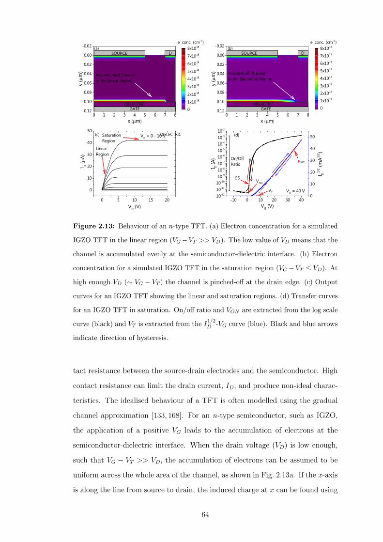
0 5 10 15 20
0
10
20
30
40
50
0 1 2 3 4 5 6 7 80.12
0.10
0.08
0.06
0.04
0.02
0.00
-0.02
DIELECTRIC
x ( m)
y (
m)
0
1x10¹⁸
2x10¹⁸
3x10¹⁸
4x10¹⁸
5x10¹⁸
6x10¹⁸
7x10¹⁸
8x10¹⁸
e- conc. (cm-3)
SOURCE
GATEDIELECTRIC
D
Accumulated Channel in the Linear Region
0
10
20
30
40
50
SAT
SSVON
I D1/
2 (m
A1/
2)
On/Off Ratio
VT
0 1 2 3 4 5 6 7 80.12
0.10
0.08
0.06
0.04
0.02
0.00
-0.02
Pinched-off Channel in the Saturation Region
x ( m)
y (
m)
0
1x10¹⁸
2x10¹⁸
3x10¹⁸
4x10¹⁸
5x10¹⁸
6x10¹⁸
7x10¹⁸
8x10¹⁸
e- conc. (cm-3)
SOURCE
GATEDIELECTRIC
D
-10 0 10 20 30 4010-12
10-11
10-10
10-9
10-8
10-7
10-6
10-5
10-4
10-3
10-2
(d)(c)
(b)
VD = 40 V
VG (V)
I D (A
)
(a)
Saturation Region
VG = 0 - 10 V
I D (
A)
VD (V)
Linear Region
Figure 2.13: Behaviour of an n-type TFT. (a) Electron concentration for a simulated
IGZO TFT in the linear region (VG−VT >> VD). The low value of VD means that the
channel is accumulated evenly at the semiconductor-dielectric interface. (b) Electron
concentration for a simulated IGZO TFT in the saturation region (VG− VT ≤ VD). At
high enough VD (∼ VG − VT ) the channel is pinched-off at the drain edge. (c) Output
curves for an IGZO TFT showing the linear and saturation regions. (d) Transfer curves
for an IGZO TFT in saturation. On/off ratio and VON are extracted from the log scale
curve (black) and VT is extracted from the I1/2D -VG curve (blue). Black and blue arrows
indicate direction of hysteresis.
tact resistance between the source-drain electrodes and the semiconductor. High
contact resistance can limit the drain current, ID, and produce non-ideal charac-
teristics. The idealised behaviour of a TFT is often modelled using the gradual
channel approximation [133, 168]. For an n-type semiconductor, such as IGZO,
the application of a positive VG leads to the accumulation of electrons at the
semiconductor-dielectric interface. When the drain voltage (VD) is low enough,
such that VG − VT >> VD, the accumulation of electrons can be assumed to be
uniform across the whole area of the channel, as shown in Fig. 2.13a. If the x-axis
is along the line from source to drain, the induced charge at x can be found using
64

Q = CV , to give
Qind(x) = CG[VG − VT − φ(x)], (2.14)
where Qind is the charge induced per unit area, CG is the capacitance per unit area
of the gate dielectric layer and φ is the electrostatic potential. If the thickness
of the channel is assumed to be negligible, the induced charge can also be found
using
Qind(x) = ne(x)q, (2.15)
where ne(x) is the carrier density and q is the elementary charge. Ohm’s law
states that
J = σE
where J is the current density vector, σ is the conductivity and E is the electric
field vector. The current flows in the x-direction from source to drain along the
channel (which is assumed have negligible thickness) therefore:
J =ID(x)
Wi and E =
dφ(x )
dxi,
where W is the channel width. So Ohm’s law becomes
ID(x) = Wσdφ(x)
dx.
Using the fact that σ is related to the mobility µn by σ = neqµn gives
ID(x) = Wneqµndφ(x)
dx,
substituting in Eq. 2.15 yields
ID(x) = WµnQind(x)dφ(x)
dx.
The current must be continuous and constant throughout the channel, so inte-
grating both sides over the length of the channel gives
ID =W
Lµn
∫ L
0
Qind(x)dφ(x)
dxdx
=W
Lµn
∫ VD
0
Qind(x) dφ.
65
Substituting in Eq. 2.14 gives
ID =W
LµnCG
∫ VD
0
[VG − VT − φ(x)] dφ
=W
LµnCG
[(VG − VT )VD −
V 2D
2
]. (2.16)
When VG − VT >> VD,
ID =W
LµnCG(VG − VT )VD (2.17)
and the channel acts as a resistor with ID ∝ VD. Under these conditions the TFT
is said to be in the linear regime, as shown in Fig. 2.13c. As VD increases, the
accumulation of charge near the drain is reduced, causing the current dependence
on voltage to become non-linear. When VD = VG − VT , ID becomes independent
of VD and the TFT is said to be in saturation. Under these conditions the
potential of the drain is large enough that electrons are attracted directly to the
drain edge. This leads to depletion of the accumulated channel beneath the drain
edge, a process known as channel pinch-off which is shown in Fig. 2.13b. A quick
substitution into Eq. 2.16 gives the expression for ID in saturation:
ID =W
2LµnCG[VG − VT ]2. (2.18)
Thus, in the saturation regime ID ∝ V 2G, rather than a linear relationship.
It is worth remembering the value of ID may differ significantly from these
predictions due to defects in the channel and gate dielectric, interface traps,
leakage current and non-uniform doping [133]. However, using these equations
and the characteristics plotted in Figs. 2.13c and d, several measures of device
quality can be extracted.
2.3.3 TFT Parameters
Mobility is a key metric by which the performance of a TFT can be mea-
sured. When the electric field is low the mobility is proportional to the carrier
velocity, thus the frequency response of the TFT improves with increasing mobil-
ity. Also, higher mobility devices have higher currents that charge capacitances
more rapidly, further boosting the frequency response [116]. Moreover, if a fixed
66

current is required, higher mobilities allow for reduced device size. In displays,
smaller TFTs will take up less space in a pixel, thereby reducing the required back
light power and lowering power consumption. Scattering has a negative effect on
the mobility and can be caused by many phenomena, including but not limited
to, lattice vibrations, charges at or near the semiconductor-dielectric interface,
impurities, grain boundaries and rough surfaces at the interface [7, 116].
The mobility can be extracted from the transfer curves using two methods,
dependent on how the TFT is being operated. In the linear regime the mobility,
µLIN , is found using the following equation:
µLIN =gm
CGWLVD
.
The transconductance(gm = ∂ID
∂VG
)is taken as the gradient of the characteristic
(ID − VG curve) in the linear regime. In the saturation regime, VD ≥ VG − VT ,
the saturation mobility, µSAT , can be calculated using
µSAT =2
CGWL
[∂I
1/2D
∂VG
]2
.
A typical linear fitting on a I1/2D -VG curve is shown in Fig. 2.13d.
Subthreshold Swing (SS) reflects the change in VG required to increase ID
by an order of magnitude in the subthreshold region [133]. In essence it shows
how easily the ID is modulated by VG and can be calculated using
SS =
[d log(ID)
dVG
∣∣∣∣∣max
]−1
where the derivative is the gradient extracted from the log(ID)-VG curve, as shown
in Fig. 2.13d.
SS also gives a picture of the density of traps in the bandgap of the semicon-
ductor and at the semiconductor-dielectric interface, as illustrated in the following
equation:
SS = ln10kT
q
[1 +
q2DSG
CG
]where DSG is the density of states at EF [133]. It is possible to ascertain the
density of interface states (and thereby the density of bulk states) by varying
67

the thickness of the semiconductor film and extrapolating to a zero thickness. A
lower SS allows a TFT to operate over a smaller range of voltages, therefore DSG
is an important factor for realising high performance TFTs [66]. An interesting
result of this equation is that at room temperature SS is limited to a minimum
of ∼ 60 mV/dec.
Threshold Voltage (VT ) is the VG at which an accumulation layer is formed
in the channel region at the interface between the semiconductor and the gate
dielectric. An example of VT extraction in the saturation regime is shown in
Fig. 2.13d. By taking a linear fitting of a I1/2D − VG curve for a TFT in the
saturation regime, VT is estimated as the value of VG where the linear fit line
crosses through ID = 0. In this case, VT ∼ 7 V, but ideally, VT should be around
0 V, in order to minimise power consumption. High VT is associated with low
donor density in IGZO [169] and potentially rectifying source-drain contacts [170].
On Voltage (VON) can be defined as either the VG at which ID starts to follow
a logarithmic curve in the ID − VG plot or the VG required to fully turn off a
transistor [82]. The VON of the IGZO TFT in Fig. 2.13d is 1 V.
On/Off Ratio is simply the ratio of ID in the on state to ID in the off state
(> 108 in Fig. 2.13d). The best TFTs maximise this ratio. A higher on current
is desirable to drive pixels more efficiently, allowing for reductions in device size.
A low off-current, ideally zero, means that less power is dissipated and a TFT
switch can keep a pixel on for longer, thus reducing the required refresh rate of a
display.
Output Conductance is given by the gradient of the output curve i.e.
gd =∂ID∂VD
.
Often the reciprocal of gd, the output resistance (ro), is used. For display appli-
cations it is important to have a low output conductance in the saturation region
to prevent fluctuations in pixel intensity.
68
Transconductance is a measure of how ID varies with VG and is given by the
gradient of the transfer curve i.e.
gm =∂ID∂VG
.
Intrinsic Gain (Av) is the maximum voltage gain of a TFT. As such it is an
important measure of a TFT’s ability to amplify a signal. Furthermore, higher
values of Av also give greater noise margins in logic circuits, leading to greater
immunity to noise. Av can be calculated as the ratio of transconductance to
output conductance i.e. gm/gd or gmro.
2.3.4 IGZO TFTs
Due to the advantages of IGZO, as outlined in Section 2.1, IGZO TFTs set the
current standard for oxide semiconductor TFTs. Since the initial work of Nomura
et al., there have been many improvements and refinements made to IGZO TFTs
that have allowed them to transcend their initial electrical capabilities. Indeed,
this has led to contemporary devices with mobilities > 10 cm2/Vs, VON close to
0 V, on/off ratios exceeding 107 and subthreshold swings close to the theoretical
minimum [21,107,110,171,172].
One major area of focus for improving the quality of IGZO TFTs has been
the choice of dielectric. Binary oxide dielectrics are widely employed in TFTs
[9, 10, 124], however, their grain boundaries can serve as paths for leakage cur-
rent. Such leakage may increase the off-current of the TFT, which will af-
fect factors like pixel retention in displays. Though such issues may be miti-
gated by implementing an amorphous interfacial layer, other solutions have been
sought [168,173]. One example is multicomponent dielectrics, for example, SiO2-
Ta2O5. Though deposited at a lower temperature, the performance of these di-
electrics is comparable with SiO2 deposited via plasma-enhanced chemical vapour
deposition [174]. Furthermore, multicomponent amorphous dielectrics containing
HfO2 maintain a high dielectric constant while suppressing crystallinity and sur-
face roughness [175, 176]. The suppression of surface roughness is important for
maintaining a high mobility in the active channel. Stacked dielectrics, which
69
combine high-κ materials with larger bandgap materials, also show potential.
However, the crystalline nature of the films can still lead to charge trapping at
the interface, causing VT to drift [7].
In recent years, investigations into the use of solid-state electrolytes as gate
dielectrics have yielded TFTs with excellent device characteristics. This is due
to the formation of an electrical double layer at the interface leading to very
high gate capacitance and subsequently low operating voltages even on flexible
substrates [177–180]. Further improvements have been made through the use of
anodisation. As the oxidation of the gate metal is a self-limiting reaction, the
anodised dielectric can be very thin and have very low leakage. IGZO TFTs
with an anodised AlxOy dielectric have been shown to operate within 1 V, with
a SS = 68 mV/dec [21]. Such low operating voltages are highly desirable for
battery powered electronics.
Ohmic source-drain contacts are readily made on IGZO but their quality
can be variable dependent on the contact material [181, 182]. Most commonly
electrodes are metals, although the use of TCOs is not unusual, especially when
transparency is a consideration. Under these circumstances, ITO is often used
and is reported to have electrical properties comparable with Ti [155]. Some of
the effects of Schottky contacts on TFTs are covered in more detail in Section 2.4.
IGZO TFTs can be very sensitive to atmospheric conditions [183]. Moreover,
if the semiconductor is deposited early in the fabrication process, further fabrica-
tion steps can damage and degrade it [184]. Even when fabrication is complete,
bottom gate structures can leave the back surface of the semiconductor exposed
to the atmosphere, which can lead to instability as molecules are physisorbed
onto the semiconductor [183, 185]. These instabilities can be alleviated, but not
always cured, by the use of passivation layers, such as SiOx [184,186,187].
In rigid IGZO TFTs the substrate may also be expected to act as a gate
electrode and gate dielectric, for example, when using SiO2-Si wafers. However,
one of the main benefits of IGZO TFTs is that they can be fabricated on various
flexible substrates including plastics such as PET [10], paper [188], flexible glass
[189] and metal foil [190]. Such flexible devices have been shown to be stable
70

after bending 10,000 times [191]. Further details of research into flexible oxide
TFTs can be found in a recent review [192].
2.3.5 Applications
Work on IGZO TFTs is now increasingly geared towards applications. For exam-
ple, individual devices have been developed as sensors [15, 193, 194] and memo-
ries [14,195]. The first circuits using IGZO TFTs to challenge the benchmarks set
by a:Si-H and organic technology were 5 stage ring oscillators fabricated by Ofuji
et al. [19]. In the years that followed there was a spate of papers that improved
on this initial success. Notable examples include:
Using low processing temperature for circuits on flexible substrates [63,196].
Complementary circuits using p-type oxide semiconductors [76, 188, 197–
201].
Neural networks [202].
According to simulations, OLED pixels can be driven by TFTs with a mo-
bility > 4 cm2/Vs. Furthermore, mobilities > 2 cm2/Vs will be needed for large
LCDs with frame rates > 120 Hz, and 0.5 cm2/Vs is sufficient to drive AML-
CDs (Active Matrix Liquid Crystal Display) of less than 90 inches [18, 66]. As
IGZO now fulfils these criteria [190], large companies have actively pursued us-
ing it in large high-resolution displays. It has been predicted that 7 km2/year
of oxide semiconductor backplanes will be used in OLED displays by 2024 [203].
The incorporation of IGZO reduces the need for backlighting in displays because
the higher mobility allows for a reduced device size and the transparency allows
for the use of ambient light. For example, Samsung’s transparent LCD panels
consume 90% less electricity than conventional LCD screens [204] and the iPad
Air saw a 57% power efficiency increase as a result of employing an IGZO LCD
backplane [205].
There have also been advances made in plastic and flexible AMOLED (Active
Matrix Organic Light Emitting Diode) displays, an industry with an anticipated
market worth of $18 billion by 2020 [206]. Due to the low off-current of IGZO
71

TFTs, flexible AMOLED displays on polyimide have been shown to retain the dis-
played image for hundreds of seconds after the driver is switched off [16]. Flexible
AMOLED displays as large as 11.7 in. (Toshiba) have also been fabricated [207],
as well as e-paper [64]. With such developments in mind, several insightful dis-
cussions on the potential large scale applications of oxide semiconductors have
been written [7, 66,68,192,208].
However, there are several barriers to the wide scale adoption of IGZO TFTs.
One example is negative bias illumination stress [68]. When IGZO TFTs are held
at negative bias under illumination of near bandgap energy photons there is a
large negative shift in VT [22–30]. The instability has been attributed to the pres-
ence of deep traps formed by oxygen vacancies, although the exact mechanism
for this is still not fully understood. The near-bandgap light will excite electrons
(holes) into the conduction (valence) band. The holes will be drawn towards the
gate by the electric field and can become trapped either at the interface or in the
gate dielectric. Once the bias is removed, these holes can remain trapped, leading
to electron accumulation on the IGZO-side of the interface. While the VT shift
can be reduced by various measures including high pressure annealing [24,28,29]
and asymmetric source-drain contacts [27], it remains impractical to incorporate
IGZO into display technology without light shielding measures. Such light shield-
ing measures negate any advantages of transparency that may be offered by IGZO
as well as introducing an extra fabrication step.
Another barrier to applications is the short-channel effect, which prevents the
scaling required to produce high-density integrated circuits. In reality this is
a group of phenomena that degrade the quality of transistor characteristics as
the channel length is reduced. These include impact ionisation, channel length
modulation and contact effects. Typically, short-channel effects begin to degrade
the characteristics of IGZO TFTs when the channel length is below approximately
5 µm [31–33]. By comparison, innovative device design has allowed Si-based
devices to operate on the scale of tens of nanometres [209]. Similar innovations
are required to bridge the gap between the scalability of oxide semiconductors
and silicon.
72

2.4 Schottky Source Transistors (SSTs)
2.4.1 Introduction
Despite being invented over 70 years ago [210], new forms of transistor are still
being developed. One unconventional transistor design replaces the ohmic source
contact of a TFT with a Schottky contact. Within the literature, these devices
are given various names, such as source-gated transistors [211], Schottky barrier
thin-film transistors [99] and tunnelling contact transistors [212]. Herein, all of
these devices are referred to as Schottky source transistors (SSTs), after their
defining feature.
Significant work has been carried out on metal-oxide-semiconductor field-effect
transistors with Schottky contacts, resulting in substantial improvements in de-
vice performance, for example, enabling sub-10-nm gate lengths [213–217], and
understanding, for example, control of the shape of the Schottky source bar-
rier through variations in semiconductor thickness [218]. However, these devices
have a fundamentally different structure and operating mechanism to the thin-
film-based SST which is the focus of this section. The SST was first proposed
by Shannon and Gerstner in 2003 [211] and much of the development of SSTs
has been carried out by the same group at the University of Surrey. Control
of the current by the source contact confers several advantages upon the SST
when compared to TFTs, including low-voltage and exceptionally flat satura-
tion, high intrinsic gain and reduced sensitivity to the quality and length of the
channel [211,219–221]. These advantages, in addition to compatibility with TFT
manufacturing processes, make the SST an important development for display
technology and analogue circuits.
2.4.2 Operating Mechanism
Hindered by the lack of an agreed name, conflicting theories of SST operation
have been proposed. For example, the gate dependence of the current has been
variously attributed to lowering of the source barrier height [223], increased tun-
nelling current [99] and modulation of the effective source length [222]. There are
73

Ohmic Contact
Gate
Drain
H
I1
I2Rint
RV
DS
-ID
Source
x
z
Dielectric
Semi-
conductor
Figure 2.14: Distributed diode and resistor network model for a Schottky source
transistor, proposed by Valletta et al. [222].
also differing claims about the effects of using a Schottky drain contact [99,222].
Similarly, diode reverse current saturation [99], tunnelling [212] and depletion of
the semiconductor by the source [219] have all been suggested as causes of current
saturation.
Despite this disagreement, it is clear that the most in-depth studies of op-
erating mechanism have been carried out by Sporea and Shannon et al. at the
University of Surrey and Valletta et al. at CNR-IMM. In the design proposed by
these groups, the source region controls the current and two conditions are placed
on the structure; the gate must overlap with the source and the channel must be
sufficiently conductive to not limit the current. Conductivity in the channel can
be modulated through two means, making the gate overlap the channel so that
carriers can be accumulated/depleted at the interface or doping the channel.
It has been suggested by Valletta et al. that the region in the vicinity of the
source contact can be modelled as a distributed diode and resistor network, as
shown in Fig. 2.14 [222]. The model can effectively be divided into two separate
modes of SST operation [223]. In mode 1, the current, I1, is dominated by injec-
tion from the front edge of the source. I1 has a strong electric field dependence
due to barrier lowering mechanisms such as IFL. In mode 2 the current, I2, is
dominated by the back end of the source and is controlled by a MESFET-type
action of the depletion region at the front edge of the source. Figure 2.14 shows
how I2 is the sum of currents which are determined by a reversed biased diode
74
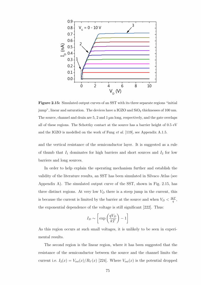
0 2 4 6 8 10
0.0
0.1
0.2
0.3
0.4
0.5
0.6
0.7
0.8
0.93
2
I D (n
A)
VD (V)
VG = 0 - 10 V
1
Figure 2.15: Simulated output curves of an SST with its three separate regions “initial
jump”, linear and saturation. The devices have a IGZO and SiO2 thicknesses of 100 nm.
The source, channel and drain are 5, 2 and 1 µm long, respectively, and the gate overlaps
all of these regions. The Schottky contact at the source has a barrier height of 0.5 eV
and the IGZO is modelled on the work of Fung et al. [119], see Appendix A.1.5.
and the vertical resistance of the semiconductor layer. It is suggested as a rule
of thumb that I1 dominates for high barriers and short sources and I2 for low
barriers and long sources.
In order to help explain the operating mechanism further and establish the
validity of the literature results, an SST has been simulated in Silvaco Atlas (see
Appendix A). The simulated output curve of the SST, shown in Fig. 2.15, has
three distinct regions. At very low VD there is a steep jump in the current, this
is because the current is limited by the barrier at the source and when VD < 3kTq
,
the exponential dependence of the voltage is still significant [222]. Thus:
ID ∼[
exp
(qVDkT
)− 1
]As this region occurs at such small voltages, it is unlikely to be seen in experi-
mental results.
The second region is the linear region, where it has been suggested that the
resistance of the semiconductor between the source and the channel limits the
current i.e. I2(x) = Vint(x)/RV (x) [224]. Where Vint(x) is the potential dropped
75

0 1 2 3 4 50.014
0.012
0.010
0.008
0.006
0.004
0.002
0.000
-0.002
0 1 2 3 4 5
0.006
0.004
0.002
0.000(b)
VG = 10 V
VD = 0.2 to 1.0 V in steps of 0.2 V
J (A
cm
-2)
x ( m)
SOURCE(a)
J (A
cm
-2)
x ( m)
VG = 0 to 10 V in steps of 1 V
VD = 0.4 V
SOURCE
Figure 2.16: Behaviour of current density under the source when in the linear region.
(a) The linear increase with VD. (b) Injection area increasing and then current injection
saturating with increasing VG.
between point x at the semiconductor-dielectric interface and the source and
RV (x) is the vertical resistance between point x and the source. This resistive
behaviour is displayed in Fig. 2.16a where the current from the source increases
linearly with VD. However, in some fabricated devices this “linear” region takes
on a more exponential curve and no satisfactory reason for this behaviour has
been given [223].
As VG increases in the linear region, the channel beneath the source becomes
increasingly conductive, leading to current injection at greater distances from the
source edge, as shown in Fig. 2.16b. This leads to gate modulation of the current
in the linear region. For high VG the channel conductance beneath the source is
high. In the simulated device, where the source is only 5µm long, this means the
whole of the source is already injecting evenly. Therefore, increases in VG do not
increase the region or magnitude of current injection. Hence, the curves become
independent of VG in the linear region i.e. the transconductance falls to zero, as
shown in Fig. 2.15.
The third region is the saturation region. The current will saturate when the
reverse biased source depletes the semiconductor below it down to the dielectric,
this is known as VDsat1 and is shown in Fig. 2.17. This also puts another constraint
on device design, the semiconductor must be thin enough be fully depleted by
the reversed bias Schottky contact. When the channel is sufficiently conductive,
76

0 1 2 3 4 5 6 7 80.12
0.10
0.08
0.06
0.04
0.02
0.00
-0.02
x ( m)
y (
m)
SOURCE
GATEDIELECTRIC
DVD < VDsat1
(a)
0 1 2 3 4 5 6 7 80.12
0.10
0.08
0.06
0.04
0.02
0.00
-0.02(b)
VD > VDsat1
Source Pinch-Off
x ( m)
y (
m)
10
11
12
13
14
15
16
17
18
19log(e- conc.) (cm-3)
SOURCE
GATEDIELECTRIC
D
Figure 2.17: Electron concentration in the semiconductor of an SST where
VG = 10 V. (a) When VD < VDsat1. (b) When VD > VDsat1 and the semiconductor-
dielectric interface is pinched-off beneath the drain end of the source.
the saturation voltage can be calculated using a two-dielectric model [219]:
VDsat1 =CG(VG − VT )
CS + CG+K (2.19)
Where CS and CG are the capacitance per unit area of the semiconductor and
insulator, respectively, while K is a constant. Firstly, it is important to note
that the value of VDsat1 is lower than the saturation in an ordinary TFT. When
saturation occurs, variations in VD should no longer affect the potential in the
region of the source contact, so I2 should remain fixed [222]. Previously, any small
increases in saturation current, IDsat, with VD have been attributed to an increase
in diffusion current from the source edge [222] or IFL (IFL is not included in the
simulations in this section) [225]. As VD increases further, the device will saturate
again, this time at the drain like an ordinary TFT, as shown in Figs. 2.13a and b.
The increase in IDsat with VG is a result of further induced charge at the
semiconductor-dielectric interface. This extra charge requires a higher VD to
deplete, leading to a current increase. The influence of VG decreases at higher
values due to reducing transconductance (see Fig. 2.15). However, it has been
suggested that at higher VG the electric field at the source edge may become large
enough to induce significant current increases, through IFL [223]. This increase
in current can lead the device to switch to mode 1 operation and lead to a rise
in transconductance.
77
2.4.3 Considerations for Device Design
There are many parameters to consider when designing SSTs, for example, the
source length and source-gate overlap. Any region of the source not overlapped by
the gate will not inject current because the channel below it will be too resistive.
Thus, the following discussion on source length assumes that the source is fully
overlapped by the gate.
The source length can affect the mode of device operation [226]. For short
sources I1 is dominant, but for longer sources the extra area allows the sum of the
weaker contributions from the rear of the source, I2, to dominate. I1 only comes
from a very small region at the front of the source and so is almost independent
of source length [227].
According to device simulations, longer sources should produce more current,
but the dependence weakens with increasing length [226, 228, 229]. This can
be explained by the distributed diode model in Fig. 2.14. Further away from
the drain end of the source there is less injection because the greater horizontal
resistance makes Vint(x) drop to zero. SSTs with longer sources are therefore
more amenable to fabrication techniques such as printing, as they have a greater
tolerance to size differences.
Longer source contacts have also been suggested as a method of reducing
the high temperature coefficient of SSTs [226]. Ordinary TFTs have a small
positive activation energy (< 0.1 eV for an IGZO TFT [230]), thus the current
rises less with temperature. If SSTs are to be used in real world applications large
fluctuations in current due to changes in temperature will make them impractical.
It was found by Sporea that the high positive temperature coefficient of the drain
current can be associated with I1, whereas I2 has a much lower temperature
coefficient. However, even with a long source the temperature coefficient of an
SST should remain greater than in a TFT.
The front edge of the contact also has a problem with self-heating, as the
high electric field leads to joule heating, although this has been shown not to be
major hurdle to device application and can be alleviated by increasing the source
length or using a field plate [231]. A field plate is an additional capacitance at
78

the front edge of the source that moves the region of high electric field away from
the source edge [225].
If high frequency operation is desired, the source length should be shortened
to reduce capacitance. In this case, the device will operate in mode 1 and most
of the current will be injected via the front 1 µm of the source. Hence the source
should be made as small as possible as the current is independent of the source
length anyway [227]. It is important to remember that shorter sources might need
a field plate to prevent the current increase at the edge when in saturation [232].
If independence of the current from source length is the only requirement, sources
longer than ∼ 100µm also satisfy this condition [226]. These longer source devices
offer a favourable design for cheaper processing techniques such as printing.
Given that the Schottky barrier at the source controls the current, the barrier
height is another major factor to consider. Too low a barrier will make it difficult
to deplete the semiconductor, as well as reducing the resistance of the source
region to the point that the channel may become the main determinant of the
current. Too high a barrier will lead to large turn-on voltage and currents too low
for application. Typical barrier heights used for SSTs are 0.3 - 0.5 eV [219, 223,
225,231], but such homogeneous low barrier heights have not been demonstrated
in oxide semiconductor Schottky junctions.
This raises another issue, thus far, all work on SSTs has assumed a homo-
geneous barrier at the source contact. Barrier inhomogeneities are prevalent in
other devices employing Schottky barriers, and they have the potential to sig-
nificantly affect the reverse current [150]. As the operating mechanism of SSTs
relies so heavily upon the behaviour of the reverse biased Schottky barrier at
the source it is important to obtain a working knowledge of the effects of source
barrier height variations.
When VD > 0, little difference was found between the use of antisymmetric
contacts (Schottky source, ohmic drain) and symmetrical source-drain (Schottky-
Schottky) SSTs [170, 222]. The choice of drain contact has limited effect on the
behaviour of an SST, Thus, source-drain contacts can be deposited simultaneously
with no detrimental effect on device performance.
79

2.4.4 Advantages and Disadvantages
Schottky contacts are often considered as having a negative effect on TFTs, but
the SST design offers many advantages. Firstly, the low voltage saturation of
SSTs, as defined by Eq. 2.19, offers a major advantage in power consumption
over TFTs. This makes them attractive for OLED displays as these are normally
driven in the saturation region so that there is tolerance for supply voltage vari-
ations [233]. In fact, simulations of LTPS SSTs showed that the SST can save
more than 60% power and reduce the layout area by more than 90% compared
to a TFT [233].
Another impressive feature of SSTs is their high intrinsic gain. Polysilicon
SSTs showed intrinsic gains greater than 1,000 for certain drain voltages, for larger
voltage ranges gains of several hundred are typical [220]. SSTs owe their high
intrinsic gain values to their high output resistance i.e. extremely flat saturation.
As previously discussed, the inability of the potential to penetrate to the saturated
source is suggested as the origin of the flat saturation. The output resistance
can be affected by barrier lowering at the source edge and this has led to the
incorporation of field plates into some devices [232]. The closer the field plate is
to the semiconductor the flatter the saturation. However, the use of a field plate
is not necessary if the device operates in mode 2, as the comparative contribution
of I1 is reduced.
Employing a Schottky barrier at the source electrode means that SST per-
formance is less sensitive to the quality of the semiconductor than standard
TFTs [221, 234]. In an ordinary TFT it is difficult to modulate the channel
resistance of semiconductors with a high carrier concentration such as IZO. More-
over, TFTs fabricated with such highly conductive semiconductors have VT < 0,
hence they must be held at negative VG in the off state, which increases power con-
sumption [235]. SSTs offer the possibility of modulating VT through the choice of
contacts, as different barrier heights will have different depletion depths [170,225].
SSTs have been shown to be independent of channel length down to 2 µm,
due to the source contact being shielded from the drain [211, 236, 237]. Such re-
sults have been corroborated by device simulations under the proviso that there
80

is no barrier lowering at the source contact [222, 238]. Furthermore, simulations
show that output resistance should remain high even when the channel is on the
sub-micron scale, however this has never been confirmed experimentally [239].
This channel independence means that accurate alignment is less of an issue in
SSTs than TFTs. Therefore, SSTs are more open to lower resolution fabrication
methods such as inkjet printing, which are useful for low cost, large-area electron-
ics because there is no need for vacuum systems or photolithography [240, 241].
Furthermore, insensitivity to alignment issues offers an addition advantage for
fabrication on flexible substrates.
SSTs using a-Si:H also showed better stability than a field-effect transistor
under forward bias stress [242]. However, there are no reports of negative bias
stress or negative bias illumination temperature stress, which is such an important
barrier to the application of IGZO transistors.
One major disadvantage of SSTs is the low drain current that they produce,
due to the reverse biased Schottky barrier at the source. This is often orders of
magnitude lower than ordinary TFTs, but simulations of SSTs suggest that it is
sufficient for use in display drivers [233]. Regardless, it would still be useful to
increase the current of SSTs without sacrificing their many benefits.
2.4.5 Applications
The SST structure has been applied to various channel layers including a-Si:H
[211,219,239], polysilicon [226,231,236], ZnO [221,237,243], ZnO nanosheets [244]
and ZnO nanowires [245]. They also bear a resemblance to the characteristics
seen in organic TFTs, where ohmic contacts are difficult to form [222,246].
High intrinsic gain and low output resistance make the SST well suited for
use in analogue and low-power circuits. Furthermore, higher values of Av also
give greater noise margins in logic circuits, leading to greater immunity to noise.
In display applications, SSTs with high output resistance can act as excellent
constant current sources. Most impressively, due to the robustness of the SST,
the current can be consistent across devices without the need for careful alignment
and patterning.
81
2.4.6 IGZO SSTs
Simulations of IGZO SSTs suggest that at a drive current of 5 µA the SST struc-
ture can save more than 60% power and reduce the layout area of a pixel driving
circuit by 25% [233]. This, combined with the many other advantages described
above, make IGZO SSTs an attractive prospect. However, until recently, attempts
at fabricating high-quality SSTs, or similar, using IGZO have yield imperfect re-
sults [170]. This is most likely due to the difficulty of forming the combined high
channel conductivity and low Schottky barrier heights required for SST operation.
In 2016 the work of Lee and Nathan, published in Science, demonstrated
an IGZO SST in all but name [99]. Low-voltage operation coupled with an
intrinsic gain of ∼ 400 demonstrated major improvements over standard IGZO
TFTs. However, the device characteristics were not entirely typical of an SST,
for example ID grew exponentially with VD prior to saturation, and despite being
high the intrinsic gain was still an order of magnitude less than the best SSTs.
Furthermore, the theoretical explanation of the unusual output curve contains
a drain-limited region at low VD, which contradicts the established literature on
SST operating mechanism. Given these results, a more in-depth understanding
of the SST operating mechanism is required. Using this knowledge a method of
maximising the intrinsic gain of oxide semiconductor SSTs should be established.
82

3 Thickness Dependence in Thin-Film Schottky
Diodes
Access to simulation software was obtained with the help of Y. Li, Y. Wang and
Q. Xin.
Geometry plays an important role in the operation of electronic devices. For
example, it is well-documented that TFTs suffer from short-channel effects [32,
33, 247, 248]. However, unlike TFTs, thin-film Schottky diodes have received
limited attention, particularly in relation to the effects of varying semiconductor
thickness. Reducing the thickness of the IGZO should have two main benefits,
firstly, the rectification ratio should increase because the forward current is limited
by the resistance of the semiconductor at higher forward biases. Thus, a thinner
semiconductor will produce a higher forward current. Secondly, the performance
of flexible devices should improve due to a reduction in tensile stress for a fixed
radius of curvature. However, some studies show evidence of a deterioration of
the reverse current with reducing thickness. For example, by comparing two
articles by IMEC, increasing the IGZO thickness from 50 nm to 100 nm leads
to an increase in rectification ratio of approximately two orders of magnitude
[42,43]. Furthermore, when the thickness is increased the barrier height increases
from 0.36 eV to 0.71 eV and the ideality factor falls slightly from 1.6 to 1.57.
Similar trends have been published, without comment, by other research groups,
including our own, but the origin of the dependence remains unexplained [17,44].
In this chapter, the significant effects of scaling IGZO thickness upon the cur-
rent density-voltage (J-V ) characteristics of thin-film Schottky diodes are pre-
sented and explained [249]. It is found that the reverse current is drastically
dependent on the IGZO thickness. With the help of device simulations per-
formed on Silvaco Atlas, the cause of this dependence is elucidated and the trend
is attributed to the inhomogeneous nature of the Schottky barrier height (ΦB).
The magnitude and area of the barrier inhomogeneities is varied to ascertain
the effects upon the reverse current of the Schottky diode. The barrier height
inhomogeneity model is also used to explain the thickness dependence of the
83
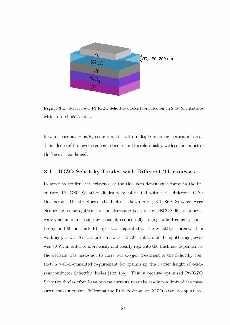
Figure 3.1: Structure of Pt-IGZO Schottky diodes fabricated on an SiO2-Si substrate
with an Al ohmic contact.
forward current. Finally, using a model with multiple inhomogeneities, an areal
dependence of the reverse current density and its relationship with semiconductor
thickness is explained.
3.1 IGZO Schottky Diodes with Different Thicknesses
In order to confirm the existence of the thickness dependence found in the lit-
erature, Pt-IGZO Schottky diodes were fabricated with three different IGZO
thicknesses. The structure of the diodes is shown in Fig. 3.1. SiO2-Si wafers were
cleaned by sonic agitation in an ultrasonic bath using DECON 90, de-ionized
water, acetone and isopropyl alcohol, sequentially. Using radio-frequency sput-
tering, a 100 nm thick Pt layer was deposited as the Schottky contact. The
working gas was Ar, the pressure was 5 × 10⁻³ mbar and the sputtering power
was 90 W. In order to more easily and clearly replicate the thickness dependence,
the decision was made not to carry out oxygen treatment of the Schottky con-
tact, a well-documented requirement for optimising the barrier height of oxide
semiconductor Schottky diodes [122, 156]. This is because optimised Pt-IGZO
Schottky diodes often have reverse currents near the resolution limit of the mea-
surement equipment. Following the Pt deposition, an IGZO layer was sputtered
84

-1.0 -0.5 0.0 0.5 1.010-7
10-6
10-5
10-4
10-3
10-2
10-1
100
101
102
2x10⁻¹⁰
2x10⁻⁹
2x10⁻⁸
2x10⁻⁷
2x10⁻⁶
2x10⁻⁵
2x10⁻⁴
2x10⁻³
2x10⁻²
2x10⁻¹
-0.5 0.5-1.0 0.0 1.0
0
2x10¹³
4x10¹³
6x10¹³
8x10¹³ (b)
IGZO Thickness
50 nm
150 nm
250 nm
|I| (A
)
|J| (A
cm
-2)
V (V)
(a)
Thickness = 250 nm
Frequency = 100 kHz
C-2
(cm
4 F-2
)
V (V)
Figure 3.2: (a) |J |-V characteristics of devices with IGZO thicknesses of 50, 150 and
250 nm. (b) C−2-V curve for the 250 nm thick IGZO diode from which the carrier
density ND was extracted.
using an IGZO target with a molar ratio of 1:1:2 (In2O3:Ga2O3:ZnO) under the
same conditions as used for Pt. Three different thicknesses of IGZO were chosen:
50, 150 and 250 nm. Al was chosen as the ohmic contact and was deposited
via thermal evaporation. The devices were patterned using shadow masks and
each sample contained diodes with three different radii: 200, 250 and 300 µm.
The current-voltage properties were measured using an Agilent E5260B semicon-
ductor analyzer. Capacitance-voltage (C-V ) measurements were carried out at
100 kHz using Agilent E4980A LCR meter; this high frequency was used as a
precaution against the influence of electron traps.
The resulting |J |-V characteristics, shown in Fig. 3.2a, display a drastic thick-
ness dependence despite the same Pt-IGZO Schottky barrier being present in all
devices. The most notable change is the huge increase in reverse current; nearly
five orders of magnitude for a 200 nm reduction in IGZO thickness, amounting
to a sharp degradation in the quality of the diodes. As a result, the rectification
ratio fell from 9.0 × 10⁴ in the 250 nm diodes to only 2.2 in 50 nm diodes de-
spite an increase in the forward current. Similar dependencies on reverse current
can be seen (without explanation) in Fig. 1f of [17] and Fig. 2a of [44], where
the authors focused on frequency response and reverse breakdown voltage, re-
spectively. Furthermore, there is a significant increase in ideality factor, n, and
a major reduction in ΦB (= qφB) as thickness is reduced. For example, in the
85

-1.00 -0.50 0.00 0.50 1.0010-7
10-6
10-5
10-4
10-3
10-2
10-1
100
101
102
Diode Radius 250 mm 200 mm
-1.00 -0.50 0.002x10⁻⁵
4x10⁻⁵
6x10⁻⁵
8x10⁻⁵
10-41.2x10-41.4x10-41.6x10-41.8x10-42x10-4
|J| (
A c
m-2
)
V (V)
|J| (
A c
m-2
)
V (V)
Figure 3.3: |J |-V characteristics of Pt-IGZO Schottky diodes with radii of 200 and
250 µm.
diodes with 250 nm of IGZO, ΦB = 0.64 eV and n = 1.40, but for diodes with
150 nm of IGZO, ΦB = 0.51 eV and n = 1.48. The sharp deterioration of the
|J |-V characteristics meant that no fitting was possible for the 50 nm devices.
The series resistance of the diodes is 31.3, 27.5 and 31.3 Ωcm−2 for the 50, 150
and 250 nm thick IGZO diodes respectively.
An explanation for this thickness dependence is not possible using thermionic
emission theory (as discussed in Section 2.2.4), where:
J = A∗T 2 exp
(− ΦB
kT
)[exp
(qV
nkT
)− 1
]where A∗ = 4πqm∗k2
h3is the Richardson constant (≈ 41 A cm−2 K−2 in IGZO),
m∗ is the effective mass of an electron, k is the Boltzmann constant, q is the
fundamental charge, h is the Planck constant, V is the applied bias and T is
the temperature. According to this equation, the current should only be depen-
dent upon ΦB and V (for a set material and a fixed temperature). In addition,
thermionic emission theory presupposes a flat reverse current, but between−0.2 V
and −1 V the reverse current increases by 636%, 265% and 169% for the 50, 150
and 250 nm thick cases, respectively. The only anticipated thickness dependence
86

Property Symbol Value
Relative permittivity εs 10
Bandgap EG 3.05 eV
Electron affinity χSC 4.16 eV
Conduction band effective density of states NC 5× 1018 cm−3
Valence band effective density of states NV 5× 1018 cm−3
Electron mobility µn 15 cm2/Vs
Hole mobility µp 0.1 cm2/Vs
Richardson Constant for Electrons A∗ 41 A cm−2 K−2
Table 3.1: Default properties of IGZO used in Silvaco Atlas simulations.
in the experimental data is at high forward bias. In this regime the current is
limited by the series resistance, hence thinner semiconductor layers yield higher
currents.
In Fig. 3.2b, the flattening out of the C−2-V curve shows how the Schottky
diode becomes fully-depleted in reverse bias. The shallow gradient of the plot
when V < 0 may be a result of the Al doping the IGZO at the ohmic contact [37].
As the bias becomes more positive the depletion region shrinks and Eq. 2.5 can
be used to show that ND = 6× 1013 cm−3. There was no hysteresis in the C−2-V
curve and the value of ND was frequency independent.
The diodes also display no thickness dependence of the current density, as
shown by Fig. 3.3. Indeed, when reverse biased at V = -1 V, there is a variation
of less than 3 × 10⁻⁵ A cm−2 between the plotted samples. This result suggests
that edge effects do not make a significant contribution to the current, for further
discussion of this issue see Section 3.4.
3.2 Possible Reasons for Thickness Dependence
In the interest of clarifying the possible origins of this behaviour, two-dimensional
device simulations were carried out using Silvaco Atlas (details on Silvaco Atlas
can be found in Appendix A). The modelled diodes have a width of 100 nm and
87

-1.0 -0.5 0.0 0.5 1.010-7
10-6
10-5
10-4
10-3
10-2
10-1
100
101
102
0.00 0.05 0.10 0.15 0.20 0.25-1.0
-0.5
0.0
0.5
1.0(b)
IGZO Thickness
50 nm
150 nm
250 nm
|J| (
A c
m-2
)
V (V)
(a)
E C (e
V)
z ( m)
B0.64 eV
ND = 6 x 1013 cm-3
V = -1 V
Ec - EF
Scho
ttky
Con
tact
Ohmic Contact
Figure 3.4: (a) |J |-V curves for simulated diodes with IGZO thicknesses of 50, 150
and 250 nm. (b) Profiles of the conduction band minimum for simulated diodes with
IGZO thicknesses of 50, 150 and 250 nm.
semiconductor thicknesses of 50, 150 and 250 nm, unless stated otherwise. The
Schottky barrier height was set in accordance with the results extracted from
the |J |-V curve of the 250 nm thick diode (0.64 eV) and the doping was set
in accordance with the experimental results extracted from the C−2-V curve in
Fig. 3.2b, i.e. ND = 6×1013 cm−3. The IGZO parameters used in this section are
displayed in Table 3.1 [250]. The mesh density within the IGZO layer was finer
nearer the Schottky interface and was fixed for all thicknesses. The main focus of
this section is the reverse current, as this is where the change in semiconductor
thickness has the most dramatic effect.
3.2.1 Diffusion Theory
Figure 3.4a shows the simulated |J |-V characteristics of diodes with different
thicknesses of IGZO. In this case, there is a clear trend showing that for reducing
thickness there is an increase in reverse current. However, the increase is less than
one order of magnitude, which is inconsistent with the large difference seen in the
experimental results. The comparatively small variation in reverse current can be
accounted for by considering the diffusion equation (see Section 2.2.5 and [133]):
J ≈ qµnNCEM exp
(− ΦB
kT
)[exp
(qV
kT
)− 1
].
88

-1.0 -0.5 0.0 0.5 1.010-7
10-6
10-5
10-4
10-3
10-2
10-1
100
101
102
B = 0.64 eV
ND = 6 x 1013 cm-3
Image Force Lowering Enabled
|J| (
A c
m-2
)
V (V)
IGZO Thickness 50 nm 150 nm 250 nm
Figure 3.5: |J |-V curves for simulated diodes demonstrating the effect of thickness
with the inclusion of image force lowering.
Here, µn is the carrier mobility, NC is the effective density of states in the con-
duction band and EM is the electric field at the Schottky interface. Although
there is no change in ΦB for different thicknesses of IGZO, as shown in Fig. 3.4b,
there is an increase in the gradient of the conduction band minimum (EC) with
reducing thickness. As
E =1
q∇EC ,
reducing the thickness leads to an increase in EM and a subsequent increase
in reverse current. The magnitude of the increase in reverse current is much
smaller than that observed in the experimental results in Fig. 3.2a because the
dependence of current upon semiconductor thickness is approximately linear (see
Section 4.2.2 for full theory).
3.2.2 Image Force Lowering
A well-known cause of bias dependence in the reverse current is image force
lowering (IFL), the origins of which are discussed in Section 2.2.3. The image
force is dependent on the electric field, which in standard diodes does not have
a thickness dependence. However, in thin-film diodes, the semiconductor can be
fully depleted in reverse bias and thus the electric field can increase with reducing
89
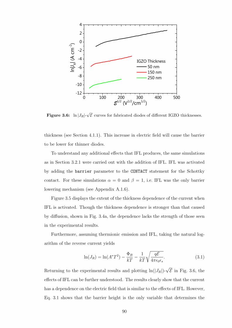
0 100 200 300 400 500-12
-10
-8
-6
-4
-2
0
2
4
IGZO Thickness 50 nm 150 nm 250 nm
ln|J
R| (
A c
m-2
)
E1/2 (V1/2/cm1/2)
Figure 3.6: ln |JR|-√E curves for fabricated diodes of different IGZO thicknesses.
thickness (see Section 4.1.1). This increase in electric field will cause the barrier
to be lower for thinner diodes.
To understand any additional effects that IFL produces, the same simulations
as in Section 3.2.1 were carried out with the addition of IFL. IFL was activated
by adding the barrier parameter to the CONTACT statement for the Schottky
contact. For these simulations α = 0 and β = 1, i.e. IFL was the only barrier
lowering mechanism (see Appendix A.1.6).
Figure 3.5 displays the extent of the thickness dependence of the current when
IFL is activated. Though the thickness dependence is stronger than that caused
by diffusion, shown in Fig. 3.4a, the dependence lacks the strength of those seen
in the experimental results.
Furthermore, assuming thermionic emission and IFL, taking the natural log-
arithm of the reverse current yields
ln(JR) = ln(A∗T 2)− ΦB
kT− 1
kT
√qE
4πε0εs. (3.1)
Returning to the experimental results and plotting ln(|JR|)-√E in Fig. 3.6, the
effects of IFL can be further understood. The results clearly show that the current
has a dependence on the electric field that is similar to the effects of IFL. However,
Eq. 3.1 shows that the barrier height is the only variable that determines the
90

-1.0 -0.5 0.0 0.5 1.010-7
10-6
10-5
10-4
10-3
10-2
10-1
100
101
102
IGZO Thickness 50 nm 150 nm 250 nm
|J| (
A c
m-2
)
V (V)
UST Enabled
Figure 3.7: |J |-V curves for simulated diodes demonstrating the effect of thickness
with the inclusion of tunnelling.
intercept point, thus if IFL was the dominant cause of the thickness dependence
all of the plots would have the same intercept. From a linear fitting of the plots
the different barrier heights are extracted as 0.42, 0.54 and 0.66 eV for the 50,
150 and 250 nm cases, respectively. Thus, it can be concluded that IFL is not
the dominant cause of the thickness variation seen in the experimental results.
3.2.3 Tunnelling
Another factor that may contribute to a thickness dependence and non-ideal
diode behaviour is tunnelling. Different diode thicknesses were simulated using
the inbuilt Universal Schottky Tunnelling (UST) mechanism in Silvaco Atlas (see
Appendix A.1.7). This method calculates the tunnelling current at each grid
point near the Schottky contact. The effective mass of the electron in IGZO was
taken to be 0.34 me [251], where me is the rest mass of an electron, and all other
parameters remained the same as in Section 3.2.1. The resulting |J |-V curves
are shown in Fig. 3.7. The figure shows that tunnelling produces a stronger
thickness dependence than diffusion and IFL, but again, not as strong as the
experimental results. Indeed, when V = −1 V the current in the 50 nm diode is
20.6 times larger than the 250 nm diode. In the experiment this same thickness
91

-0.0013 -0.0006 0.0001-31
-29
-27
-25
-23
-21
-19
-17IGZO Thickness
50 nm
150 nm
250 nm
1/E (cm/V)
ln|J
R/E
2 | (A
/V2 )
Figure 3.8: ln |JR/E2|-1/E curves for fabricated diodes of different thicknesses.
reduction produces a current variation of 9.0×10⁴. This vast discrepancy suggests
that tunnelling is not a sufficient explanation for the phenomena observed in the
experiment.
Furthermore, as Fig 3.2b shows that the fabricated diodes are fully depleted
when under reverse bias, the semiconductor can effectively be treated as a dielec-
tric. According to Sze [133], under these circumstances
J ∼ E2 exp
[− 4√
2m∗Φ3/2B
3qhE
].
Thus, ln(JR/E2) ∝ 1/E if tunnelling is the dominant transport mechanism. How-
ever, Fig. 3.8 shows that the ln(JR/E2)-1/E plots of the experimental results are
non-linear for all thicknesses. Therefore, it must be concluded that the thickness
dependence of the reverse current is not predominantly caused by tunnelling.
3.2.4 Anode Roughness
Previously, the deterioration of the reverse bias in Pd-IGZO Schottky diodes has
been attributed to the roughness of the metal anode [252]. Changes in the an-
nealing treatment of the substrate and the Schottky contact gave rise to different
anode roughnesses and a variation in reverse current of around two orders of
magnitude when V = −1 V. Anode roughness may play a greater role in diodes
with a thinner semiconductor layer. Device simulations were carried out to test
92
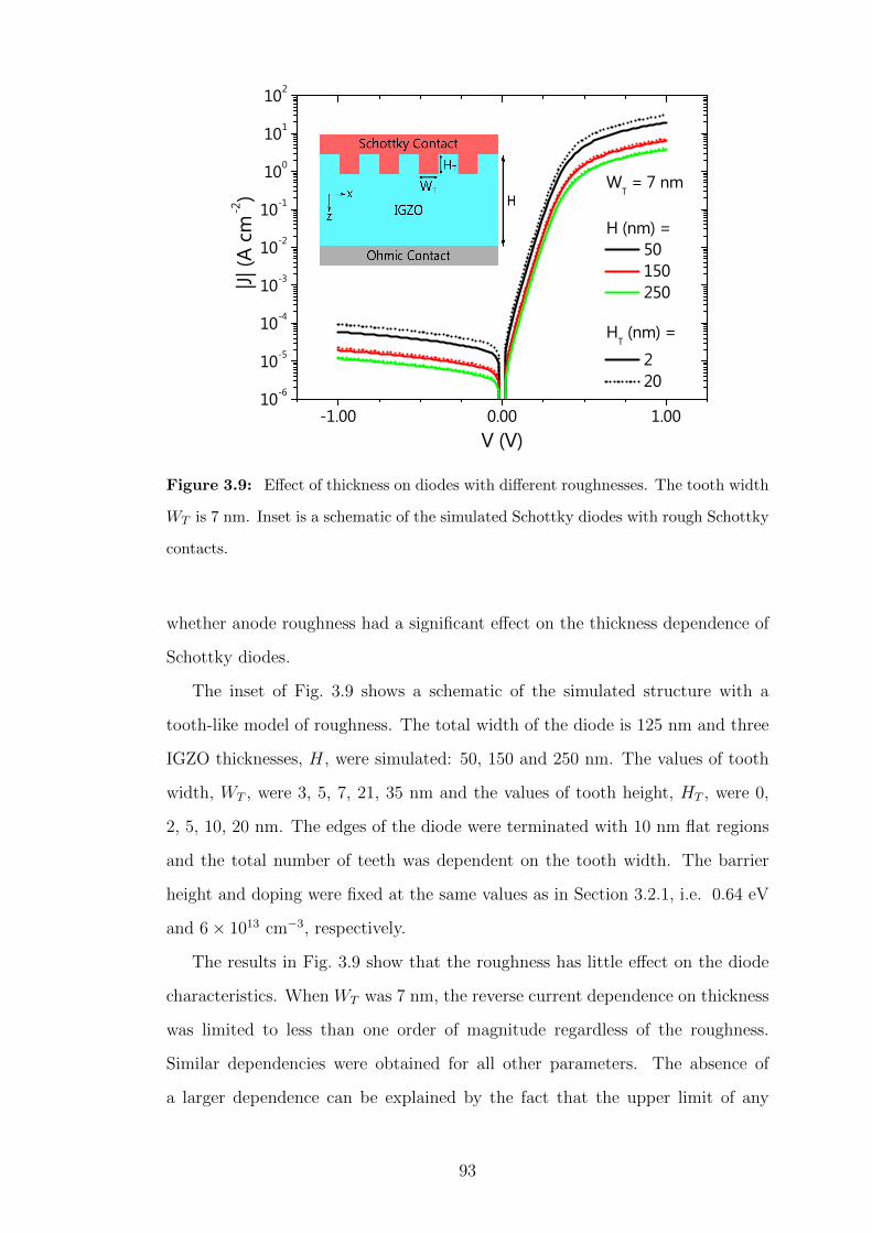
-1.00 0.00 1.0010-6
10-5
10-4
10-3
10-2
10-1
100
101
102
WT = 7 nm
H (nm) = 50 150 250
HT (nm) =
2 20
|J| (
A c
m-2
)
V (V)
Figure 3.9: Effect of thickness on diodes with different roughnesses. The tooth width
WT is 7 nm. Inset is a schematic of the simulated Schottky diodes with rough Schottky
contacts.
whether anode roughness had a significant effect on the thickness dependence of
Schottky diodes.
The inset of Fig. 3.9 shows a schematic of the simulated structure with a
tooth-like model of roughness. The total width of the diode is 125 nm and three
IGZO thicknesses, H, were simulated: 50, 150 and 250 nm. The values of tooth
width, WT , were 3, 5, 7, 21, 35 nm and the values of tooth height, HT , were 0,
2, 5, 10, 20 nm. The edges of the diode were terminated with 10 nm flat regions
and the total number of teeth was dependent on the tooth width. The barrier
height and doping were fixed at the same values as in Section 3.2.1, i.e. 0.64 eV
and 6× 1013 cm−3, respectively.
The results in Fig. 3.9 show that the roughness has little effect on the diode
characteristics. When WT was 7 nm, the reverse current dependence on thickness
was limited to less than one order of magnitude regardless of the roughness.
Similar dependencies were obtained for all other parameters. The absence of
a larger dependence can be explained by the fact that the upper limit of any
93
thickness dependence is determined by the diffusion current, which only has a
weak thickness dependence.
In the real device it may be the case that the roughness has a more jagged
profile, leading to points on the anode where there is a high electric field. However,
given that the roughness of Pd contacts in [252] are extremely small compared to
the diode thickness (root mean square roughness < 1 nm in all cases), it remains
unlikely that this is a significant factor that directly contributes to such large
variations in reverse current.
3.2.5 Inhomogeneous Barrier Height
Though roughness appears not to be a direct contributor to the thickness depen-
dence of the current, different crystal faces of the metal may be exposed as a
result of roughness. These crystal faces will have varying surface atom densities,
leading to a spatial variation in the metal work function. A multitude of experi-
mental methods have been used to show that the work function of different crystal
faces of the same metal can vary over hundreds of meV [139,146,147]. These ex-
perimentally observed variations have been corroborated by theoretical studies
and ab initio calculations [253,254]. As the Pt Schottky contact deposited in the
experiment is likely to be polycrystalline, different crystal faces will be in contact
with the IGZO, leading to variations in the Schottky barrier height. Roughness,
among other factors, may also lead to the formation of dangling bonds and traps
at the interface. Interface traps can potentially have a significant effect upon the
Schottky barrier height by pinning the Fermi-level, indeed, for many materials the
Schottky barrier height is dictated by interface states [136,255]. More specifically
relating to the work in this thesis, control of interfacial oxygen is important for
achieving high-quality oxide semiconductor Schottky diodes [41,122,156]. More-
over, the amorphous nature of IGZO may lead to local variations in the electron
affinity and the density of interface states, further increasing the disorder at the
interface. All of these factors are potential contributors to variations of the Schot-
tky barrier height over different regions of the diode and it has been recognised
that such variations can lead to non-ideal J-V characteristics [140,150].
94

Schottky Contact
0.00 0.01 0.02 0.03 0.04 0.050.1
0.2
0.3
0.4
0.5
0.6
0.7
0.00 0.01 0.02 0.03 0.04 0.050.1
0.2
0.3
0.4
0.5
0.6
0.7
-1.0 -0.5 0.0 0.5 1.010-710-610-510-410-310-210-1100101102
0.00 0.02 0.04 0.06 0.08 0.10
0.25
0.20
0.15
0.10
0.05
0.00
(c) (d)
(b)
0.0
8.8x10 -4
1.8x10 -3
2.6x10 -3
3.5x10 -3
4.4x10 -3
|J| (A cm -2)LBR
x ( m)
z (
m)
0B 0.64 eV
= 0.36 eVV = -1 V
Ohmic Contact
HBR
150 nm
250 nm
E C (e
V)
z ( m)
150 nm
50 nm
50 nm
250 nmV = 0 V
V = -1 V
E C (e
V)
z ( m)
Scho
ttky
Con
tact
Scho
ttky
Con
tact
IGZO Thickness
50 nm 150 nm
250 nm
|J| (A
cm
-2)
V (V)
(a)
Figure 3.10: (a) Contour plot of |J | in a Schottky diode with an LBR in the Schottky
contact (cross hatched region) and an IGZO thickness of 250 nm. The diode is under
reverse bias (V = −1 V) and the LBR has a barrier height of ΦB = Φ0B −∆ = 0.28 eV.
(b) Profiles of EC beneath the LBR at V = 0 V for Schottky diodes with 50, 150 and
250 nm thick IGZO layers. (c) The same profiles as in (b) but for V = −1 V. (d)
Corresponding |J |-V curves for the Schottky diodes in (b) and (c).
In order to account (at least qualitatively) for a spatially varying Schottky
barrier height, a lower barrier region (LBR) was included in the centre of the
simulated Schottky contact. The LBR is illustrated by the cross hatched region
of Schottky contact in Fig. 3.10a. In Fig. 3.10 the LBR has a width of L0 =
10 nm and in this region the mean barrier height (Φ0B) is reduced by a value
of ∆ = 0.36 eV. These values for L0 and ∆ represent one of a few different
circumstances that reflect the large variations in current seen in the experiment
while remaining within realistic variations of metal work function as outlined in
the literature [146,147].
Figure 3.10a shows a contour plot of |J | for a simulated 250 nm thick IGZO
95
device for V = −1 V. It is clear from this image that the reverse current is
dominated by the contribution from the LBR. To elucidate the behaviour of EC
in this region, vertical cutlines of the simulated structures were taken through
the semiconductor at x = 0.05µm. The EC profiles in the higher barrier regions
(HBRs), where ΦB = Φ0B, display the same behaviour as seen in the homogeneous
diode in Fig. 3.4b. However, Fig. 3.10b shows that when V = 0 V, saddle points
are formed in the EC profiles below the LBR. These saddle points in EC are
formed due to the potential below the HBRs influencing the potential below the
LBR [148,150]. Saddle points are not always formed below the LBR and criteria
for their formation in thin-film diodes is derived in Section 4.3.1. Regardless of
whether a saddle point is formed, the maximum value of EC beneath the LBR
(ECM) will act as an effective barrier height for the LBR. As the LBR is the
main determinant of the current, ECM will act as an effective barrier height for
the whole diode. When V = 0 V, ECM is 0.47, 0.53 and 0.55 eV for the 50, 150
and 250 nm diodes, respectively. Even at zero bias, the built-in electric field in
the 50 nm diode is much higher than in the thicker diodes. As such, the thinner
diodes will have lower saddle points. A similar trend is displayed in Fig. 3.10c,
where V = −1 V. In this case, ECM is 0.32, 0.44 and 0.48 eV for the 50, 150 and
250 nm diodes, respectively. Hence, in the 250 nm diode, ECM is three-quarters
of Φ0B (the barrier height in the HBR), but in the 50 nm diode ECM is only half
of Φ0B. As the reverse current is proportional to exp(−ECM
kT), the strong thickness
dependence of ECM leads to a reverse current increase of over 400 times (when
V = −1 V) as the IGZO thickness is reduced from 250 to 50 nm, as shown in
Fig. 3.10d. Furthermore, changing the bias from V = 0 V to V = −1 V leads
to changes in ECM of 0.14, 0.09 and 0.07 eV for the 50, 150 and 250 nm cases,
respectively. Thus, ECM in thinner diodes is more easily reduced by increasing
reverse bias, which explains the steeper gradients of the reverse current in thinner
diodes seen in Fig. 3.10d. Similar changes in ECM in forward bias can be used to
explain the thickness dependencies of extracted values of ΦB and n, which will
be discussed in Section 3.3.
The simulation results in Fig. 3.10 qualitatively reproduce the trends seen in
96

-0.1 0.0 0.1 0.2 0.3 0.4 0.5 0.6 0.7
0.2
0.3
0.4
0.5
0.6
0.7
-0.1 0.0 0.1 0.2 0.3 0.4 0.5 0.6 0.710-5
10-4
10-3
10-2
10-1
100
101
102
0 10 20 30 40 500.2
0.3
0.4
0.5
0.6
0 10 20 30 40 5010-5
10-4
10-3
10-2
10-1
100
101
0B
-
150 nm
0B
0.64 eV
(d)(c)
(b)
L0 = 10 nm
V = -1 V0B
-
E CM (e
V)
(eV)
(a)
250 nm
150 nm
50 nm
|J| (A
cm
-2)
(eV)
0B
0.64 eV
L0 = 10 nm
V = -1 V
E CM (e
V)
L0 (nm)
0B
0.64 eV
= 0.36 eVV = -1 V
150 nm
250 nm
250 nm
50 nm
50 nm
0B
0.64 eV
= 0.36 eVV = -1 V
|J| (A
cm
-2)
L0 (nm)
250 nm
150 nm50 nm
Figure 3.11: Effects of variations in inhomogeneity magnitude and size upon the re-
verse biased EC profiles and current densities of Schottky diodes with IGZO thicknesses
of 50, 150 and 250 nm. The dotted blue lines indicate the value of ECM when there is
no saddle point present i.e. ECM = Φ0B −∆. (a) ECM against ∆ for L0 = 10 nm and
V = −1 V. (b) |J | against ∆ for L0 = 10 nm and V = −1 V. (c) ECM against L0 for
∆ = 0.36 eV and V = −1 V. (d) |J | against L0 for ∆ = 0.36 eV and V = −1 V.
the experiments in Fig. 3.2a and in [17, 42–44], particularly the orders of mag-
nitude differences in reverse current. Exact fitting of the experimental results is
hampered by the simplicity of the model. Firstly, real diodes are likely to con-
tain many inhomogeneities with a broad distribution of areas and barrier heights
dependent on various factors including which Pt crystal faces are exposed, the
amorphous nature of IGZO and the presence of contaminants. Furthermore, even
if it were possible to model such complexity, the range of variables would be too
large to achieve a meaningful fitting.
To account for different experimental conditions, the effects of varying ∆ and
L0 upon ECM and reverse current were considered. The value of ∆ was varied
from 0 to 0.60 eV in 0.12 eV increments, while five different values of L0 were
97

used: 2, 5, 10, 20 and 50 nm. Figure 3.11 demonstrates that increasing the size
and reducing the barrier height of the LBR will give rise to lower values of ECM
and lead to significantly larger current densities in reverse bias. Furthermore,
the figure demonstrates that these effects are far more pronounced in the thinner
diodes.
Figure 3.11a shows that for fully depleted thin-film diodes, increasing ∆ has a
far more significant effect on the ECM of thinner devices. This is because it is more
difficult for the HBRs to pinch-off the LBR in thinner devices, as demonstrated
by the fact that no saddle point is formed in the 50 nm case for low values of ∆.
Lower values of ∆ also have a very weak dependence of ECM on IGZO thickness,
but as ∆ increases this thickness dependence grows stronger. Hence, the thickness
dependence of the reverse current will be exacerbated at higher values of ∆, as
shown in Fig. 3.11b. Given the orders of magnitude differences in reverse current
seen in Fig. 3.2a, it is clear that the results are more closely described by large
values of ∆, i.e. large variations in barrier height.
Figures 3.11c and d show that in the limit where L0 is very small, the thickness
dependence of ECM , and therefore the reverse current, is also small. This stands
to reason as smaller inhomogeneities will be more easily pinched-off and regardless
of semiconductor thickness ECM tends to Φ0B as L0 tends to zero. It becomes
harder to pinch-off the LBR as L0 gets larger, hence the thickness dependence
strengthens. At very large values of L0, no saddle point is formed and current
transport will tend to a limit where the HBR and LBR effectively conduct as
diodes in parallel. This parallel conduction will lead the reverse current to behave
as if it were a low barrier diode with barrier height ΦB = Φ0B − ∆ and an area
equal to that of the LBR. In this limit there will be a weak thickness dependence
akin to the one shown in Fig. 3.4a. Thus, as the results display a very strong
thickness dependence of the reverse current, they are unlikely to conform to either
of these limiting cases.
98

3.3 Effects of Barrier Height Inhomogeneities on Forward
Current
Although the thickness dependence is strongest in reverse bias, the inhomoge-
neous barrier hypothesis also needs to explain the weaker dependence of the
forward bias. In the experimental results displayed in Section 3.1 the extracted
barrier height decreased and the ideality factor increased with reducing thickness.
3.3.1 Barrier Height
In inhomogeneous diodes ΦB has a significant voltage dependence [148,150]. How-
ever, to simplify the analysis of the thickness dependence, ΦB was extracted at
V = 0.2 V, a high enough value to avoid the effects of thermal fluctuations and
low enough to avoid the effects of series resistance. The choice of ∆ = 0.36 eV is
arbitrary and similar behaviours can be seen for other values.
Figure 3.12a shows how ΦB varies with H and L0. In this case, ΦB is extracted
according to thermionic emission theory, as is typical of barrier height analysis in
IGZO Schottky diodes. Regardless of the value of L0, ΦB reduces with reducing
thickness and the dependence becomes stronger as H gets smaller, just as in the
experimental results. Given that the current is dominated by the LBR, even at
these low forward voltages, the large variation of ΦB with H must be the result
of the behaviour of the barrier in the vicinity of the LBR.
By taking cutlines below the centre of the LBR, profiles of EC were obtained,
as shown in Fig. 3.12b. It is clear that the saddle point is still present at low
forward bias. Due to the weaker electric field in the thicker semiconductor devices,
saddle point formation is easier, leading to higher saddle points and thus higher
extracted ΦB for thicker diodes. The values of ECM 0.53, 0.57 and 0.58 eV for
50, 150 and 250 nm, respectively, demonstrate that the thickness dependence of
ECM is stronger for thinner semiconductors. This explains the steeper reductions
in ΦB with reducing thickness.
The results show that barrier height estimation in thin-film Schottky diodes is
further complicated by the thickness dependence. Extraction from |J |-V curves
99
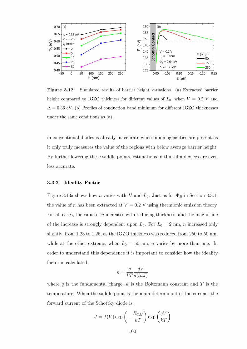
-50 0 50 100 150 200 2500.40
0.45
0.50
0.55
0.60
0.65
0.70
0.00 0.05 0.10 0.15 0.20 0.250.25
0.30
0.35
0.40
0.45
0.50
0.55
0.60
B (e
V)
H (nm)
= 0.36 eVV = 0.2 VL0 (nm)=
2 5 10 20 50
(a) (b)
E C (e
V)
z ( m)
V = 0.2 VL0 = 10 nm
0B 0.64 eV
= 0.36 eV
H (nm) = 50 150 250
Scho
ttky
Con
tact
Figure 3.12: Simulated results of barrier height variations. (a) Extracted barrier
height compared to IGZO thickness for different values of L0, when V = 0.2 V and
∆ = 0.36 eV. (b) Profiles of conduction band minimum for different IGZO thicknesses
under the same conditions as (a).
in conventional diodes is already inaccurate when inhomogeneities are present as
it only truly measures the value of the regions with below average barrier height.
By further lowering these saddle points, estimations in thin-film devices are even
less accurate.
3.3.2 Ideality Factor
Figure 3.13a shows how n varies with H and L0. Just as for ΦB in Section 3.3.1,
the value of n has been extracted at V = 0.2 V using thermionic emission theory.
For all cases, the value of n increases with reducing thickness, and the magnitude
of the increase is strongly dependent upon L0. For L0 = 2 nm, n increased only
slightly, from 1.23 to 1.26, as the IGZO thickness was reduced from 250 to 50 nm,
while at the other extreme, when L0 = 50 nm, n varies by more than one. In
order to understand this dependence it is important to consider how the ideality
factor is calculated:
n =q
kT
dV
d(lnJ)
where q is the fundamental charge, k is the Boltzmann constant and T is the
temperature. When the saddle point is the main determinant of the current, the
forward current of the Schottky diode is:
J = f(V ) exp
(− ECM
kT
)exp
(qV
kT
)100

-50 0 50 100 150 200 2501.0
1.5
2.0
2.5
3.0
3.5
4.0
0.00 0.05 0.10 0.15 0.20 0.250.45
0.50
0.55
0.60
0.65
0.70
0.75
0.80V = 0.2 V
0B 0.64 eV
=0.36 eVL0 (nm)=
2 5 10 20 50
n
H (nm)
(a) (b) H = 250 nm
L0 = 10 nm0B 0.64 eV
= 0.36 eV
E C (e
V)
z ( m)
V (V) = 0.15 0.20 0.25
Scho
ttky
Con
tact
H = 50 nm
Figure 3.13: Simulated results of ideality factor variations. (a) Extracted ideality
factor compared to IGZO thickness for different values of L0, when V = 0.2 V and
∆ = 0.36 eV. (b) Profiles of conduction band minimum for 50 and 250 nm IGZO at
forward biases of 0.15, 0.20 and 0.25 V, under the same conditions as (a).
where f(V ) is a function dependent on whether the current transport is
thermionic emission or diffusion limited. Therefore:
n =
(1 +
kT
q
d(lnf)
dV− 1
q
dECMdV
)−1
(3.2)
so, the stronger the voltage dependence of ECM , the larger n will be.
Figure 3.13b takes the voltage dependence of ECM into consideration. The
values of EC directly below the centre of the LBR are plotted for H = 50 and
250 nm, with three different bias points V = 0.15, 0.2 and 0.25 V for each. There
are saddle points present in all of the plots, but the maximum point has a stronger
bias dependence in the case where H = 50 nm. This stronger bias dependence
for the thinner device explains the increase in n with reducing thickness for the
case where L0 = 10 nm. For the same change in applied voltage, the electric field
change is larger in the thinner devices, leading to a greater effect on the saddle
point.
For some situations very thin devices may have no saddle point, while thicker
ones do. When there is no saddle point, the value of ECM is fixed regardless
of the applied voltage. Hence, these thin devices will have a lower n than the
thicker devices with a saddle point. Such results are only likely to occur when L0
is large.
These results indicate that saddle points were present for all fabricated diodes
101

in Section 3.1. In IGZO Schottky diodes the barrier height is likely to vary
significantly over small areas because of variations on different length scales e.g.
oxygen vacancies, cation concentrations, metal work function and the various
interface states that may result from contamination. The role of oxygen vacancies
is quite easily tested by treating the contact with oxygen. In fact, it is well
known that oxygen treatment improves the quality of Schottky contacts on oxide
semiconductors [41, 122, 156]. The effects of the metal work function may be
investigated by changing the choice of metal contacts, however, the more subtle
issue of how the work function varies with the crystal faces of each metal may
be harder to explore, though Kelvin probe force microscopy may be used as a
starting point. The effects of varying IGZO cation concentrations on the interface
are less well known and would require the fabrication of many devices as there is
a large parameter space.
3.4 Multiple Inhomogeneities
In real devices, the barrier height variations are likely to occur across the whole
area, A, of the Schottky contact rather than simply be localised in the centre.
To help understand the effects of multiple inhomogeneities in barrier height, de-
vice simulations using Silvaco Atlas were carried out. Due to limitations with
the software it is difficult to simulate a large-scale, Gaussian distributed set of
barrier heights, hence a simple alternating barrier model was designed, as shown
in Fig. 3.14. In this model, the Schottky contact is made up of alternating re-
gions of low barrier height (ΦB = Φ0B − ∆), labelled A, and high barrier height
(ΦB = Φ0B), labelled B. The high barrier regions (HBRs) have a width of 990 nm
and the low barrier regions (LBRs) have a width of L0 = 10 nm. Of particular
note is the LBR at the left edge of the Schottky contact, in previous simulations
all LBRs were surrounded by HBRs.
In Fig. 3.15, the results of the simulation show that there is an areal depen-
dence of the reverse current density. The strength of the areal dependence is
strongly affected by ∆ and H. Thinner films and smaller inhomogeneity mag-
nitude lead to a weaker areal dependence. Moreover, the areal dependence of
102

Width Ratio : = 1:99
= LBR
= HBRIGZO
Ohmic Contact
H
Figure 3.14: Schematic showing the alternating barrier model of the Schottky diode.
The top Schottky contact consists of alternating low and high barrier regions (LBRs
and HBRs) with an area ratio of 1:99.
the current density also weakens with increasing area, as highlighted by the plots
when ∆ = 0.36 eV where the areal dependence is almost absent at larger areas.
Theories of the areal dependence of the current density in nano-scale Schottky
diodes have previously been proposed [256,257], however, such a dependence has
been shown to exist in larger diodes where these theories do not apply [41, 258].
Such large-scale dependencies have been attributed to “local current conduction
paths” [258], but how these lead to an areal dependence of the current density
remains unexplained. Furthermore, there has been no discussion of a related
thickness dependence.
To investigate the origins of the areal dependence, and how it is affected by
different parameters, profiles of the current density across the Schottky contact
were taken. Figure 3.16 shows profiles of the current density across the Schottky
contact in two different diodes when V = −1 V. Fig. 3.16a, where H = 500 nm
and ∆ = 0.36 eV, represents the diodes with a linear dependence between the
current density and the area. In this case, the current contribution from the
LBR at the edge dominates, peaking at over 10 A cm−2, compared to around
10−3 A cm−2 for the LBR in the centre. Moreover, a significant amount of current
from the LBR at the edge travels along the top surface of the semiconductor
and then down towards the ohmic contact (as shown by the non-zero |J | values
between 0 < x < 1 µm), meaning the edge dominance is even stronger than the
103

1 10 10010-6
10-5
10-4
10-3
10-2
10-1
100
0
B= 0.64 eV
L0 = 100 nm
ND = 6 x 10
13 cm
-3
V = -1 V (eV), H (nm):
0.12, 50 0.12, 100 0.12, 200 0.12, 500 0.36, 50 0.36, 100 0.36, 200 0.36, 500
|J| (
A c
m-2
)
Area ( m2)
Figure 3.15: Simulated results for the areal dependence of the reverse current density
(V = −1 V) in inhomogeneous Schottky diodes with different semiconductor thicknesses
(H = 50, 100, 200 and 500 nm) and inhomogeneity magnitudes ∆ = 0.12 and 0.36 eV.
comparison of peak values suggests. The edge dominance of the current explains
the linear dependence of the current density. If the edges dominate then the total
current should be almost independent of area. Therefore, for two different diodes
with areas A′ and A′′: A′J ′ = A′′J ′′. Thus, the gradient of the log(|J |)− log(A)
plot is:
m =log(J ′′/J ′)
log(A′′/A′)=
log(A′/A′′)
log(A′′/A′)= −1
which fits the simulated results for when ∆ = 0.36 eV and 100 < H < 500 nm in
Fig. 3.15.
By comparison, in Fig. 3.16b, where H = 50 nm, ∆ = 0.12 eV, the sum of
the contributions of the LBRs in the centre is comparable with the contribution
from the edge. If the area is large enough, then the contribution from the centre
of the diode will dominate and the log(|J |) − log(A) curve will saturate. The
beginning of the transition from edge dominated to centre dominated can be seen
in the H = 50 nm, ∆ = 0.36 eV plot in Fig. 3.15, where the |J |-A dependence
starts to weaken at higher A. The opposite end of the transition is represented
in the plots when ∆ = 0.12 eV. Here, a weak |J |-A dependence can be seen for
smaller areas. Obtaining data for a full transition from edge dominated to centre
104

0 10 20 30 40 50 6010-10
10-8
10-6
10-4
10-2
100
102
0 10 20 30 40 50 6010-6
10-4
10-2
100
0.0 0.2 0.4 0.6 0.8 1.010-10
10-8
10-6
10-4
10-2
100
102
32.99 33.00 33.01 33.0210-10
10-8
10-6
10-4
10-2
100
102
0.7 0.8 0.9 1.0 1.110-7
10-6
10-5
10-4
10-3
10-2
10-1
32.99 33.00 33.01 33.0210-7
10-6
10-5
10-4
10-3
10-2
10-1
0B = 0.64 eV, L 0 = 10 nm, H = 500 nm , = 0.36 eV, V = -1 V
|J| (A
cm
-2)
x ( m)
(a)
Schottky Contact
Schottky Contact
(b)
|J| (A
cm
-2)
x ( m)
0B = 0.64 eV, L 0 = 10 nm, H = 50 nm, = 0.12 eV, V = -1 V
|J| (A
cm
-2)
x ( m)
LBR
|J| (A
cm
-2)
x ( m)
LBR
|J| (A
cm
-2)
x ( m)
LBR
|J| (A
cm
-2)
x ( m)
LBR
Figure 3.16: Reverse current density (V = −1 V) through the Schottky contact under
different conditions. (a) Schottky diode with H = 500 nm, ∆ = 0.36 eV displays edge
dominant behaviour. (b) Schottky diode with H = 50 nm, ∆ = 0.12 eV displays centre
dominant behaviour. Both (a) and (b) show the contribution of the inhomogeneities
at the edge (left) and centre (right).
dominated requires a larger range of areas which was not possible due to the limit
on the number of nodes available in the simulation software.
The factors that lead to the areal dependence can be traced to the saddle point
in EC formed under the LBR. Regardless of the conditions, the LBR at the edge
will not be pinched-off because it is not surrounded by regions of higher barrier
height. However, as mentioned in Section 3.2.5, when an LBR is surrounded
by HBRs the formation of the saddle point is dependent on factors such as the
105

inhomogeneity magnitude, the inhomogeneity width and the thickness of the
semiconductor. When a saddle point is formed and there is a large difference
between the saddle point height ECM and Φ0B − ∆ (the barrier height at the
edge LBR), the centre of the contact will inject significantly less current than
the edge, where no saddle point is formed. Hence, for a fixed area, the current
is more likely to be dominated by edge contributions when the semiconductor is
thick and ∆ is large (as this is where the discrepancy between ECM and Φ0B −∆
is greatest, see Fig. 3.11a), just like in Fig. 3.16a. Reducing the thickness of the
semiconductor reduces the saddle points leading to a greater contribution from
the centre of the Schottky contact. Thus, when the semiconductor is thinner a
smaller area:perimeter ratio is required for current contributions from the centre
of the Schottky contact to dominate.
3.5 Summary
In summary, a strong thickness dependence of the current in thin-film Schottky
diodes has been identified and explained. The most notable feature of the de-
pendence is the dramatic increase in reverse current for thinner semiconductor
layers. While factors such as diffusion, IFL and tunnelling do produce a thickness
dependence, device simulations indicate that the observed dependence is due to
inhomogeneities in Schottky barrier height. Variations in the Schottky barrier
height can occur as a result of several factors including the exposure of differ-
ent metal crystal faces, the use of disordered semiconductors and contamination.
Such variations in barrier height lead to the formation of saddle points in the con-
duction band minimum due to depletion from surrounding higher barrier regions.
As the saddle point energy represents a local minimum of the barrier height, in
most cases the current passing over the saddle points will make the dominant
contribution to the diode current. Devices with a thinner semiconductor layer
have a higher electric field, leading to a reduction of the saddle point energy
and therefore greater current. The thickness dependence of the saddle point is
the origin of the observed increasing reverse current and reducing effective bar-
rier height with reducing thickness. Device simulations also demonstrated that
106

thinner diodes are more sensitive to variations in the magnitude and size of in-
homogeneities. Furthermore, the greater bias dependence of saddle points in the
thinner devices leads to an increase in ideality factor with reducing thickness.
Finally, in the presence of multiple inhomogeneities an areal dependence of the
current density is observed, which explains some of the results in the literature.
The combined effects of varying area and thickness were probed and it was found
that thinner films reduce the range of areas for which the current density is area
dependent.
As thin-film electronics matures, disordered materials (e.g. IGZO and organic
semiconductors) and less rigid processing (e.g. printing) will become common-
place. As such, the issue of defects in thin-film electronics will become ever more
prevalent and understanding the underlying physics of these issues will become
crucial to device design. The findings in this chapter may have implications
not only for diode design and optimisation, but also for other thin-film device
structures, such as SSTs and MESFETs.
107

4 Analytical Theory of Thin-Film Schottky
Diodes
Access to simulation software was obtained with the help of Y. Li, Y. Wang and
Q. Xin.
Device design is highly dependent upon a detailed understanding of the ef-
fects of changes in geometry and material choices. In Chapter 3, it was found that
the combination of thin-films and interfacial disorder produces previously unex-
plained behaviour in Schottky diodes. In order to obtain a deeper understanding
of these effects, it is worthwhile to develop an analytical theory of thin-film Schot-
tky diode behaviour.
The theory of a metal-semiconductor junction proposed in Section 2.2 assumes
several conditions which are not always fulfilled in practical devices. For example,
in thin-film technology, Schottky diodes can be fully depleted. Furthermore, as
discussed in Section 3.2.5, barrier height inhomogeneities can have a significant
effect on device characteristics. In both cases, an analytical theory for these
devices is required to better understand their behaviour. In this chapter, a theory
for fully depleted thin-film Schottky diodes, including barrier inhomogeneities, is
presented and compared with the results of simulations. Particular attention is
paid to the reverse bias behaviour, which is often the limiting factor in rectification
ratio and can be dramatically affected by the semiconductor thickness.
The structure of the Schottky diodes considered in this chapter is shown in
Fig. 4.1. The modelled diodes are made up of a three-layered structure with an
ohmic contact on the bottom, the semiconductor in the middle and a Schottky
contact on top. The interface between the Schottky contact and the IGZO is at
z = 0, the interface between the ohmic contact and the IGZO is at z = H and the
centre of the diode is at x = 0. The model assumes a symmetry in the y-direction
and has a depth, Ly. The total width of the diode, Lx, is 100 nm.
The simulations in this chapter are carried out in Silvaco Atlas [250]. Atlas
iteratively solves discrete differential equations based on Maxwell’s equations at
each node of a user-defined grid, further details can be found in Appendix A. As
108

Ohmic Contact
IGZO H
x
z
Schottky Contact
Figure 4.1: Structure of the Schottky diode model with a homogeneous barrier height.
a result, the simulations are physically accurate provided that accurate material
parameters, e.g. mobility, and physical models, e.g. carrier scattering, are included
by the user. Beyond the requirement to include all the correct physical models,
the number of nodes is limited to a maximum of 20,000, while a large number
of nodes leads to a large computing time. Regardless, device simulations are less
time consuming than experiments and offer insight that is difficult or impossible to
obtain experimentally. The simulation parameters used in this chapter are based
on the parameters outlined by Fung et al. [119,250], see Table A.1 in Appendix A.
The mesh density within the IGZO layer was fixed for all thicknesses and was
denser near the Schottky interface in order to resolve finer detail.
4.1 Potential in a Thin-Film Schottky Diode
In Section 2.2, only Schottky diodes with semiconductor thicknesses larger than
the depletion width, WD, are considered. In a fully depleted thin-film Schottky
diode, just as in Schottky diodes fabricated using bulk materials, the conduction
band minimum can be found using
∇2φ = −qND
ε0εs(4.1)
where φ is the electrostatic potential, ND is the donor concentration, ε0 is the
permittivity of free space and εs is the relative permittivity. Given the model in
Fig. 4.1, Eq. 4.1 can be reduced to one-dimension such that
d2φ
dz2= −qND
ε0εs.
109

As the semiconductor region is fully depleted, the boundary conditions from
Section 2.2 are changed to
φ(0) = −φB
and
φ(H) = −(φn + V ),
where φB is the Schottky barrier height (in terms of the potential), H is the
semiconductor thickness, φn is the Fermi potential from the conduction band
edge, i.e. −(EC − EF )/q, and V is the applied bias. Hence, the potential in the
semiconductor is
φ(z) = −φB −qND
2ε0εsz2 +
(φbi − VH
+qND
2ε0εsH
)z (4.2)
where φbi = φB − φn is the built-in potential. As a result, the conduction band
minimum is given by
EC(z) = qφB +q2ND
2ε0εsz2 −
(q(φbi − V )
H+q2ND
2ε0εsH
)z. (4.3)
Figure 4.2a displays the conduction band minimum for 50 nm thick Schottky
diodes with ND varying from 1013 to 1017 cm−3 and applied biases of 0, -0.5 and
-1 V. These plots show that EC is dominated by its linear component and the
quadratic term in Eq. 4.3 is comparatively weak. The dominance of the linear
component for small H is to be expected, as z is very small. However, as H
tends to WD the dominance of the linear term should wane because the thin-
film model of EC should tend to the parabolic depletion approximation given
by Eq. 2.2. Figure 4.2b shows that the analytical expression for EC in Eq. 4.3
fits the simulation results for EC for different thicknesses of semiconductor when
H < WD.
By differentiating Eq. 4.3, the electric field in the semiconductor is obtained:
E(z) =qND
ε0εsz − φbi − V
H− qND
2ε0εsH. (4.4)
As H and z are small, thinner films will produce a higher electric field, matching
the results discussed in Section 3.2.1 (particularly Fig. 3.4). Moreover, E = 0
when H = z = WD (using Eq. 2.3), demonstrating that the thin-film diode
110

0.00 0.01 0.02 0.03 0.04 0.05
-1.0
-0.5
0.0
0.5
1.0
0.0 0.1 0.2 0.3 0.4 0.5
0.2
0.4
0.6
0.8
1.0 (b)B = 0.94 V
H = 50 nmB = 0.94 V
V = 0 VND = 1015 cm-3
V (V) = 0 -0.5 -1
E C (e
V)
z ( m)
ND (cm-3) =
1013
1014
1015
1016
1017
(a)
Scho
ttky
Con
tact
Ohm
ic C
onta
ct
Theory Simulation
E C (e
V)
z ( m)
H (nm)= 20 50 200 500
EC - EF
Scho
ttky
Con
tact
Ohm
ic C
onta
ct
Figure 4.2: Conduction band minimum, EC , in a fully depleted IGZO Schottky diode.
(a) Calculated effects of varying doping and applied bias upon EC in a 50 nm thick
diode. (b) Comparison of theory and simulation of EC for different thicknesses.
theory is compatible with the standard depletion approximation. The value of
the electric field at the Schottky junction is given by
E(0) = −φbi − VH
− qND
2ε0εsH
thus
|E(0)| = EMT =φbi − VH
+qND
2ε0εsH
where EMT is the maximum electric field in a fully depleted Schottky diode.
4.1.1 Image Force Lowering
As discussed in Section 2.2.3, the Schottky barrier height can be reduced due to
an image charge effect known as image force lowering (IFL). By following the
same derivation, the barrier lowering potential in a thin-film Schottky diode is
φIFL =
√qEMT
4πε0εs=
√q
4πε0εs
(φbi − VH
+qND
2ε0εsH
).
Although the dependence of φIFL upon the electric field is the same as standard
IFL, the electric field in the fully-depleted thin-film diode has a dependence on
the thickness. Hence, thinner diodes will have lower barrier heights and the
dependence strengthens as H gets smaller, as shown in Fig 4.3. For example,
in the 100 nm thick diodes the barrier lowering can be more than a factor of
six larger than the compared to the value predicted by the standard depletion
111

0 100 200 300 400 5000.00
0.02
0.04
0.06
0.08
0.10B = 0.94 V
V = 0 VND (cm-3) =
1013
1014
1015
IFL (e
V)
H (nm)
Figure 4.3: Image force lowering in a fully depleted Schottky diode for different
semiconductor thicknesses and carrier concentrations.
approximation. As H gets larger and tends to WD the thickness dependence
weakens and φIFL tends to the thickness independent value given in Eq. 2.6.
4.2 Current Transport in Fully Depleted Thin-Film
Schottky Diodes
As discussed in Section 2.2, there are several different mechanisms for transport
across a Schottky barrier. The dominant current limiting mechanism is dependent
on factors such as the materials used to form the junction, the device geometry,
the applied bias and the temperature.
4.2.1 Thermionic Emission Current
Considering the current density from thermionic emission without IFL is ex-
pressed as
J = A∗T 2 exp
(− qφB
kT
)[exp
(qV
kT
)− 1
]it is clear that none of the parameters are affected by the changes to the shape
of the barrier outlined in Section 4.1. Thus, the thermionic emission current in a
fully depleted diode is exactly the same as predicted for the standard depletion
approximation.
112
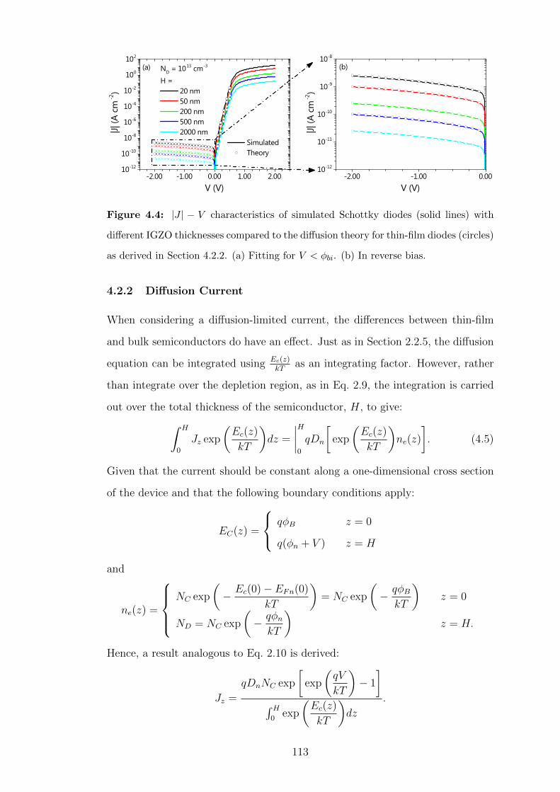
-2.00 -1.00 0.00 1.00 2.0010-12
10-10
10-8
10-6
10-4
10-2
100
102
-2.00 -1.00 0.0010-12
10-11
10-10
10-9
10-8
(b)
Simulated Theory
ND = 1013 cm-3
H = 20 nm 50 nm 200 nm 500 nm 2000 nm
|J| (A
cm
-2)
V (V)
(a)
|J| (A
cm
-2)
V (V)
Figure 4.4: |J | − V characteristics of simulated Schottky diodes (solid lines) with
different IGZO thicknesses compared to the diffusion theory for thin-film diodes (circles)
as derived in Section 4.2.2. (a) Fitting for V < φbi. (b) In reverse bias.
4.2.2 Diffusion Current
When considering a diffusion-limited current, the differences between thin-film
and bulk semiconductors do have an effect. Just as in Section 2.2.5, the diffusion
equation can be integrated using Ec(z)kT
as an integrating factor. However, rather
than integrate over the depletion region, as in Eq. 2.9, the integration is carried
out over the total thickness of the semiconductor, H, to give:∫ H
0
Jz exp
(Ec(z)
kT
)dz =
∣∣∣∣H0
qDn
[exp
(Ec(z)
kT
)ne(z)
]. (4.5)
Given that the current should be constant along a one-dimensional cross section
of the device and that the following boundary conditions apply:
EC(z) =
qφB z = 0
q(φn + V ) z = H
and
ne(z) =
NC exp
(− Ec(0)− EFn(0)
kT
)= NC exp
(− qφB
kT
)z = 0
ND = NC exp
(− qφnkT
)z = H.
Hence, a result analogous to Eq. 2.10 is derived:
Jz =
qDnNC exp
[exp
(qV
kT
)− 1
]∫ H
0exp
(Ec(z)
kT
)dz
.
113
Substituting in the value for EC (Eq. 4.3) gives
Jz =
qDnNC exp
(− qφB
kT
)[exp
(qV
kT
)− 1
]∫ H
0exp
[q2ND
2ε0εskTz2 −
(q(φbi − V )
kTH+
q2ND
2ε0εskTH
)z
]dz
From Eq. 4.4, the bottom integral can be rewritten as:
Int. ≈∫ H
0
exp
[qE(z)
kTz
]dz
The electric field is quite constant throughout the semiconductor, as shown by
the linearity of the conduction band in Fig. 4.2. Thus, E(z) can be replaced with
E(0) without significantly reducing the accuracy of the model, giving:
Int. ≈∫ H
0
exp
[qE(0)
kTz
]dz ≈
[qEMT
kT
]−1
Thus, the current density can be expressed as
Jz ≈q2DnNC
kT
(φbi − VH
+qND
2ε0εsH
)exp
(− qφB
kT
)[exp
(qV
kT
)− 1
]≈ qµnNCEMT exp
(− qφB
kT
)[exp
(qV
kT
)− 1
](4.6)
which is comparable to the standard diffusion equation (Eq. 2.11), except that
EM is replaced by EMT .
The |J |−V characteristics calculated using Eq. 4.6 are compared to simulated
results in Fig. 4.4. The thickness of IGZO was varied over two orders of magnitude
(H = 20, 50, 200, 500 and 2000 nm) and ND = 1013 cm−3. The theory is
an excellent fit for all of the different thicknesses when V < φbi (in this case
φbi = 0.6 V) and the thickness dependence of the current, as discussed in
Section 3.2.1, is clearly reproduced.
The difference between the extracted barrier heights using the thin-film dif-
fusion theory developed here (φB,TFD) and standard diffusion theory (φB,D) can
be expressed as
φB,TFD − φB,D =kT
qln
[EMT (0)
EM(0)
].
In Fig. 4.5, the difference between the two is mapped with respect to H and ND
for φB = 0.94 V. The white regions are where the thin-film approximation does
114
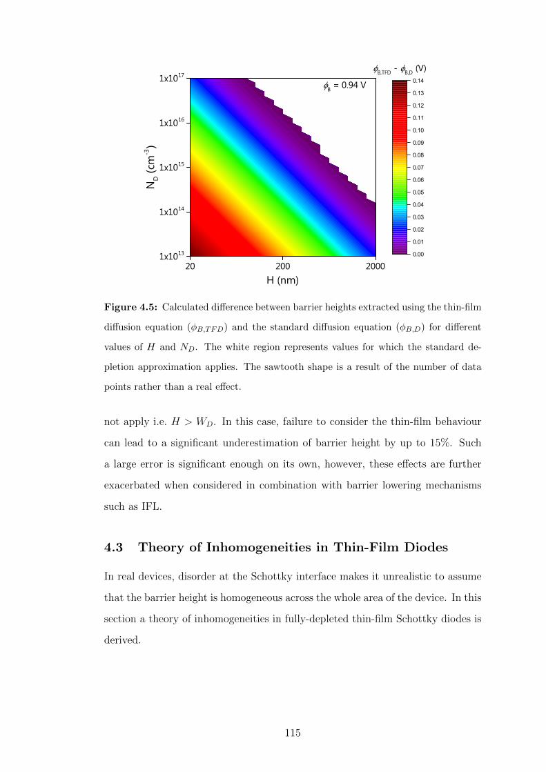
20 200 20001x1013
1x10¹⁴
1x10¹⁵
1x10¹⁶
1x10¹⁷
H (nm)
ND (c
m-3)
0.00
0.01
0.02
0.03
0.04
0.05
0.06
0.07
0.08
0.09
0.10
0.11
0.12
0.13
0.14B,TFD
- B,D
(V)
B = 0.94 V
Figure 4.5: Calculated difference between barrier heights extracted using the thin-film
diffusion equation (φB,TFD) and the standard diffusion equation (φB,D) for different
values of H and ND. The white region represents values for which the standard de-
pletion approximation applies. The sawtooth shape is a result of the number of data
points rather than a real effect.
not apply i.e. H > WD. In this case, failure to consider the thin-film behaviour
can lead to a significant underestimation of barrier height by up to 15%. Such
a large error is significant enough on its own, however, these effects are further
exacerbated when considered in combination with barrier lowering mechanisms
such as IFL.
4.3 Theory of Inhomogeneities in Thin-Film Diodes
In real devices, disorder at the Schottky interface makes it unrealistic to assume
that the barrier height is homogeneous across the whole area of the device. In this
section a theory of inhomogeneities in fully-depleted thin-film Schottky diodes is
derived.
115

Figure 4.6: Geometry of the dipole sheet approximation and related simulations for
fully depleted thin-film Schottky diodes.
4.3.1 Potential
Figure 4.6 shows a version of the dipole sheet model employed by Tung [149] and
discussed in Section 2.2.6 which has been modified to include thickness variations.
Adding the dipole sheet approximation term, φsheet, in Eq. 2.12 to the thin-film
potential in Eq. 4.2 gives:
φ(x, z) =− φ0B −
qND
2ε0εsz2 + EMT z +
δ
π
[arctan
( |x|+ L0
2
z
)− arctan
( |x| − L0
2
z
)]where the centre of the inhomogeneity is at x = 0, L0 is the width of the inho-
mogeneity and δ is the difference between the mean barrier height, φ0B, and the
barrier height of the inhomogeneity. Hence the conduction band minimum is
EC(x, z) = qφ0B +
q2ND
2ε0εsz2 − qEMT z
− qδ
π
[arctan
( |x|+ L0
2
z
)− arctan
( |x| − L0
2
z
)](4.7)
and
EC(0, z) = qφ0B +
q2ND
2ε0εsz2 − qEMT z −
2qδ
πarctan
(L0
2z
)(4.8)
is the conduction band minimum directly below the centre of the inhomogeneity.
Figure 4.7 shows a comparison of the analytical expression for EC(0, z) in Eq. 4.8
and simulated results for different thicknesses of IGZO (H = 20, 50, 200 and
116
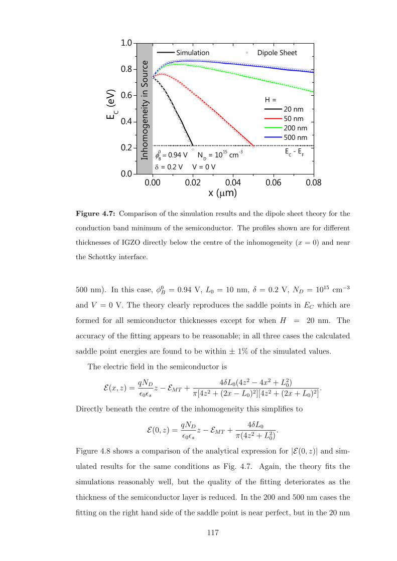
0.00 0.02 0.04 0.06 0.080.0
0.2
0.4
0.6
0.8
1.0 Simulation Dipole Sheet
0
B0.94 V N
D = 1015 cm-3
= 0.2 V V = 0 V
E C (e
V)
x ( m)
H = 20 nm 50 nm 200 nm 500 nm
EC - E
FInho
mo
gen
eity
in S
our
ce
Figure 4.7: Comparison of the simulation results and the dipole sheet theory for the
conduction band minimum of the semiconductor. The profiles shown are for different
thicknesses of IGZO directly below the centre of the inhomogeneity (x = 0) and near
the Schottky interface.
500 nm). In this case, φ0B = 0.94 V, L0 = 10 nm, δ = 0.2 V, ND = 1015 cm−3
and V = 0 V. The theory clearly reproduces the saddle points in EC which are
formed for all semiconductor thicknesses except for when H = 20 nm. The
accuracy of the fitting appears to be reasonable; in all three cases the calculated
saddle point energies are found to be within ± 1% of the simulated values.
The electric field in the semiconductor is
E(x, z) =qND
ε0εsz − EMT +
4δL0(4z2 − 4x2 + L20)
π[4z2 + (2x− L0)2][4z2 + (2x+ L0)2].
Directly beneath the centre of the inhomogeneity this simplifies to
E(0, z) =qND
ε0εsz − EMT +
4δL0
π(4z2 + L20).
Figure 4.8 shows a comparison of the analytical expression for |E(0, z)| and sim-
ulated results for the same conditions as Fig. 4.7. Again, the theory fits the
simulations reasonably well, but the quality of the fitting deteriorates as the
thickness of the semiconductor layer is reduced. In the 200 and 500 nm cases the
fitting on the right hand side of the saddle point is near perfect, but in the 20 nm
117

0.00 0.02 0.04 0.06 0.080
1x10⁵
2x10⁵
3x10⁵
4x10⁵
5x10⁵
0
B0.94 V
ND = 1015 cm-3
= 0.2 VV = 0 VH =
20 nm 50 nm 200 nm 500 nm
|E| (
V/c
m)
z ( m)
Simulation Dipole Sheet
Inho
mo
gen
eity
in S
our
ce
Figure 4.8: Comparison of simulation results and the dipole sheet theory for the
electric field in the semiconductor. The profiles shown are for different thicknesses of
IGZO directly below the centre of the inhomogeneity (x = 0) and near the Schottky
interface.
case the maximum electric field is ∼ 8% higher in the theory (3.45× 10⁵ V/cm)
than the simulation (3.20×10⁵ V/cm). Discrepancies like this will invariably have
an effect upon the accuracy of any diffusion current theory, but not thermionic
emission theory, where the electric field is not taken into account.
The saddle point in EC only exists under certain circumstances, as discussed
in Section 3.2.5. When the saddle point exists the conduction band minimum
must increase with z from x = z = 0, so
∂EC∂z
∣∣∣∣(x,z)=(0,0)
= −qEMT +4qδ
πL0
> 0
therefore
EMT <4δ
πL0
. (4.9)
Thus, increasing the width of the inhomogeneity makes it less likely for a saddle
point to form and reducing δ does the same, offering an analytical underpinning
for the simulated results in Section 3.2.5. A less obvious dependency is that
of the semiconductor thickness, however, in most cases the 1/H term of EMT
118

is dominant so thinner semiconductor layers are less likely to produce a saddle
point, further confirming the experimental results.
The position of the saddle point, zs, can be calculated using the fact that
E(0, zs) = 0:
0 =qND
ε0εszs − EMT +
4δL0
π(4z2s + L2
0).
Ignoring the highest order z term, equivalent to assuming the homogeneous com-
ponent of the barrier is triangular, yields
zs ≈
√δL0
πEMT
−(L0
2
)2
which can be substituted into Eq. 4.8 to obtain ECM .
4.3.2 Thermionic Emission Current
When the condition for a saddle point to be formed (Eq. 4.9) is not met, the
regions of the Schottky diode with different barrier heights may be modelled
as diodes conducting in parallel. Therefore, when thermionic emission is the
dominant transport mechanism
I = A∗T 2 exp
(− qφ0
B
kT
)[exp
(qV
kT
)− 1
]∑i
Ai exp
(qδikT
)which in the case of the single inhomogeneity simulations presented here reduces
to
I = A∗T 2 exp
(− qφ0
B
kT
)[exp
(qV
kT
)− 1
][A1 + A2 exp
(qδ
kT
)](4.10)
where A1 is the area of the region with barrier height φ0B and A2 is the area of the
region with barrier height φ0B − δ. Importantly, this parallel conduction model
does not give rise to a thickness dependence of the current, as it is only dependent
on fixed barrier heights.
The accuracy of the parallel conduction model is displayed in Fig. 4.9. Both
the simulated and calculated |J |-V characteristics are plotted for 20 nm thick
Schottky diodes with a wide range of δ values. The choice of µn = 106 cm2/Vs in
the simulation is due to the assumption of infinite mobility in thermionic emission
theory. The theory matches the simulation almost perfectly, even for larger values
119
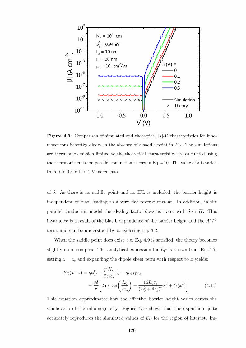
-1.0 -0.5 0.0 0.5 1.010-11
10-9
10-7
10-5
10-3
10-1
101
103
ND = 1013 cm-3
0
B = 0.94 eV
L0 = 10 nm
H = 20 nm
n = 106 cm2/Vs (V) =
0 0.1 0.2 0.3
Simulation Theory
|J| (
A c
m-2
)
V (V)
Figure 4.9: Comparison of simulated and theoretical |J |-V characteristics for inho-
mogeneous Schottky diodes in the absence of a saddle point in EC . The simulations
are thermionic emission limited so the theoretical characteristics are calculated using
the thermionic emission parallel conduction theory in Eq. 4.10. The value of δ is varied
from 0 to 0.3 V in 0.1 V increments.
of δ. As there is no saddle point and no IFL is included, the barrier height is
independent of bias, leading to a very flat reverse current. In addition, in the
parallel conduction model the ideality factor does not vary with δ or H. This
invariance is a result of the bias independence of the barrier height and the A∗T 2
term, and can be understood by considering Eq. 3.2.
When the saddle point does exist, i.e. Eq. 4.9 is satisfied, the theory becomes
slightly more complex. The analytical expression for EC is known from Eq. 4.7,
setting z = zs and expanding the dipole sheet term with respect to x yields:
EC(x, zs) = qφ0B +
q2ND
2ε0εsz2s − qEMT zs
− qδ
π
[2arctan
(L0
2zs
)− 16L0zs
(L20 + 4z2
s)2x2 +O(x4)
](4.11)
This equation approximates how the effective barrier height varies across the
whole area of the inhomogeneity. Figure 4.10 shows that the expansion quite
accurately reproduces the simulated values of EC for the region of interest. Im-
120

-10 -5 0 5 100.70
0.75
0.80
0.85
0.90
V (V) = 0 -0.5 -1 -1.5 -2
Sim Expansion
0
B0.94 V
ND = 10
15 cm
-3
= 0.2 V H = 200 nm
E C (e
V)
x (nm)
Width of LBR: L0 = 10 nm
Figure 4.10: EC in the x-direction (parallel to the Schottky contact) at the saddle
point (z = zs) for five bias points. The solid lines display the simulation results and
the dotted lines are values calculated using the expanded version of EC in Eq. 4.11.
portantly, the bias dependence of EC is also faithfully reproduced. By substitut-
ing Eq. 4.11 into the equation for thermionic emission (Eq. 2.8) and integrating
over the area of the inhomogeneity, the total current through the inhomogeneity,
Isheet, can be expressed as
Isheet ≈ A∗T 2Ly
∫ L02
−L02
exp
[− qδ
πkT
16L0zs(L2
0 + 4z2s)
2x2
]dx
× exp
− q
kT
[φ0B − EMT zs −
2δ
πarctan
(L0
2zs
)].
The solution of this integration is in terms of the error function, so to simplify
the solution the limits of integration can be changed to −∞ and +∞. Despite
this change, the solution does not deviate too far from the result if the integral
was calculated between −L0
2and L0
2because additional region of integration is at
121

the edges of the Gaussian distribution. Therefore
Isheet ≈ A∗T 2Ly
∫ ∞−∞
exp
[− qδ
πkT
16L0zs(L2
0 + 4z2s)
2x2
]dx
× exp
− q
kT
[φ0B − EMT zs −
2δ
πarctan
(L0
2zs
)]≈ A∗T 2πLy(L
20 + 4z2
s)
4
√kT
qδL0zs
× exp
− q
kT
[φ0B − EMT zs −
2δ
πarctan
(L0
2zs
)]From this equation the effective area of the inhomogeneity is
Aeff =πLy(L
20 + 4z2
s)
4
√kT
qδL0zs
and the effective barrier height for the inhomogeneity is
φB,eff = φ0B − EMT zs −
2δ
πarctan
(L0
2zs
). (4.12)
By summing over all of the different regions and their respective effective areas
and barrier heights the total thermionic emission current is
I = A∗T 2
[exp
(qV
kT
)− 1
]∑i
Aeffi exp
(−qφB,effi
kT
)which in the case of the simulations presented here becomes
I = A∗T 2
[A1 exp
(− qφ0
B
kT
)+Aeff exp
(− qφB,eff
kT
)][exp
(qV
kT
)− 1
]. (4.13)
The calculated |J |-V characteristics for different values of δ and H are shown
in Fig. 4.11. The plots show that the reverse current increases with increasing
reverse bias and δ, while reducing as H becomes larger. All of these dependencies
are a result of the model capturing the behaviour of the saddle point. The theory
reflects this behaviour as the second and third terms in the effective barrier height
(Eq. 4.12). Both terms make a significant contribution to barrier lowering, for
example, when H = 100 nm, δ = 0.2 V and V = −1 V, the second and third
terms lower the barrier by 0.06 and 0.12 V, respectively.
The variation of the barrier height with bias also qualitatively reproduces the
behaviour of the ideality factor seen in experiments and simulations in Chapter 3.
When δ = 0.4 V, the ideality factor (extracted at V = 0.2 V) is 1.12, 1.07 and
122
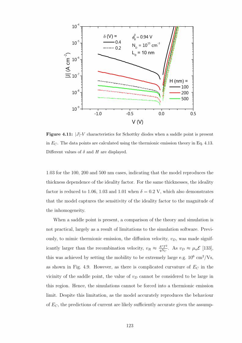
-1.0 -0.5 0.0 0.510-9
10-8
10-7
10-6
10-5
10-4
0
B0.94 V
ND = 1015 cm-3
L0 = 10 nm
(V) = 0.4 0.2
H (nm) = 100 200 500
|J| (
A c
m-2
)
V (V)
Figure 4.11: |J |-V characteristics for Schottky diodes when a saddle point is present
in EC . The data points are calculated using the thermionic emission theory in Eq. 4.13.
Different values of δ and H are displayed.
1.03 for the 100, 200 and 500 nm cases, indicating that the model reproduces the
thickness dependence of the ideality factor. For the same thicknesses, the ideality
factor is reduced to 1.06, 1.03 and 1.01 when δ = 0.2 V, which also demonstrates
that the model captures the sensitivity of the ideality factor to the magnitude of
the inhomogeneity.
When a saddle point is present, a comparison of the theory and simulation is
not practical, largely as a result of limitations to the simulation software. Previ-
ously, to mimic thermionic emission, the diffusion velocity, vD, was made signif-
icantly larger than the recombination velocity, vR ≈ A∗T 2
qNC. As vD ≈ µnE [133],
this was achieved by setting the mobility to be extremely large e.g. 106 cm2/Vs,
as shown in Fig. 4.9. However, as there is complicated curvature of EC in the
vicinity of the saddle point, the value of vD cannot be considered to be large in
this region. Hence, the simulations cannot be forced into a thermionic emission
limit. Despite this limitation, as the model accurately reproduces the behaviour
of EC , the predictions of current are likely sufficiently accurate given the assump-
123
tions made for thermionic emission. Moreover, the impossibility of forcing the
simulation into a thermionic emission limit indicates the enhanced importance of
diffusion theory in the presence of barrier height inhomogeneities.
4.3.3 Diffusion Current
The previous section focused on the effect of barrier height inhomogeneities upon
thermionic emission current. Thermionic emission is a good enough model for
semiconductors with high mobilities such as crystalline Si and GaAs, but many
emerging semiconductors, including oxides and organics, have far lower mobili-
ties. In semiconductors with a lower mobility, the effects of diffusion must be
considered.
First, consider the case where a saddle point is not present in EC . In a
similar manner to Section 4.3.2, a parallel conduction model based on the thin-
film diffusion current (Eq. 4.6) gives
I ≈ qµnNC exp
(− qφ0
B
kT
)[exp
(qV
kT
)− 1
]∑i
[AiEMTi exp
(qδikT
)].
Hence, for the simulation model used in this section (Fig. 4.6) the current can be
expressed as
I ≈ qµnNC
[A1EMT1 + A2EMT2 exp
(qδ
kT
)]× exp
(− qφ0
B
kT
)[exp
(qV
kT
)− 1
](4.14)
where A1 is the area and EMT1 is the maximum electric field in the region with
barrier height φ0B and A2 is the area and EMT2 is the maximum electric field in
the region with barrier height φ0B − δ.
A comparison of the calculated and simulated |J |-V curves for different values
of δ is shown in Fig. 4.12. The fitting is not as accurate as the parallel conduction
model for thermionic emission, but the theory is increasingly accurate as reverse
bias increases. This is because the diffusion current is strongly dependent on the
electric field, which is defined by the shape of the conduction band. Despite there
being no saddle point present, the EC beneath the inhomogeneity may still be
distorted by the higher barrier regions surrounding it, leading to variations in
124

-2.5 -2.0 -1.5 -1.0 -0.5 0.0 0.510-10
10-9
10-8
10-7
10-6
10-5
10-4
ND = 10
13 cm
-3
B
0 = 0.94 V
H = 20 nm
n = 15 cm
2/Vs
(V) 0 0.1 0.2 0.3
Simulation Theory
|J| (
A c
m-2
)
V (V)
Figure 4.12: |J |-V characteristics of the parallel conduction diffusion theory of thin-
film Schottky diodes (Eq. 4.14) and simulated results for Schottky diodes with different
values of δ and a semiconductor thickness of 20 nm.
the true value of EMT that are not captured by the simplicity of the model. As
a result, the simulated current is slightly lower than the current in the model.
Regardless of its limitations, the model does capture the dependence of the reverse
bias upon δ and the ideality factor is weakly dependent upon H as a result of the
EMT1 and EMT2 terms in Eq. 4.14.
When a saddle point is present, finding a solution is more complicated. Devel-
oping a theory akin to the one in Section 4.3.2 is more difficult because the current
is dependent upon more parameters. Consider Eq. 4.5, in the case of a diode with
a homogeneous barrier height the current density should be constant throughout
the device and Jz can be removed from the integral. However, when there is
an inhomogeneity in the barrier the problem becomes two-dimensional and the
current density becomes inhomogeneous, leading to the following equation:∫ H
0
Jz(x, z) exp
q2ND
2ε0εsz2 − qEMT z −
qδ
π
[arctan
( |x|+ L0
2
z
)− arctan
( |x| − L0
2
z
)]dz = qDnNC exp
(− qφB
kT
)[exp
(qV
kT
)− 1
].
The inclusion of an inhomogeneity in the barrier makes the problem two-
125

-1.0 -0.5 0.010-10
10-9
10-8
10-7
10-6
10-5
|J| (
A c
m-2
)
V (V)
(V) = 0.1 0.2 0.3 0.4
Simulation Theory
ND = 10
15 cm
-3
B
0 = 0.94 V
H = 200 nm
n = 15 cm
2/Vs
Figure 4.13: Diffusion limited |J |-V characteristics of inhomogeneous thin-film Schot-
tky diodes. Curves compare the theory for when a saddle point in EC is present
(Eq. 4.15) and simulated results for Schottky diodes with different values of δ and a
semiconductor thickness of 200 nm.
dimensional, hence the terms of the integral cannot be separated and the equation
cannot be solved analytically.
To overcome the impossibility of a true analytical solution, a modified parallel
conduction model was employed. The barrier height of the inhomogeneity is fixed
as ECM (the saddle point energy at x = 0) and maximum electric field for this
region is set as
EMTS =ECM − ENH − zs
where EN = EC −EF at the interface between the semiconductor and the ohmic
contact. This model assumes the electric field is constant between the saddle
point and the ohmic contact and that the region between the saddle point and
the Schottky contact behaves as an electron sink. Thus, the current can be
modelled as
I ≈ qµnNC
[exp
(qV
kT
)− 1
]∑i
[AiEMTi exp
(− ECMi
kT
)].
126

For the simulations containing a single inhomogeneity this reduces to
I ≈ qµnNC
[A1EMT1 exp
(− qφ0
B
kT
)+ A2EMTS exp
(− ECM
kT
)]×[
exp
(qV
kT
)− 1
]. (4.15)
Figure 4.13 displays a fitting of the results for a 200 nm thick semiconductor layer,
with ND = 1015 cm−3 and a range of δ. The model reproduces the increasing
reverse current with δ and as the model includes the saddle point, the dependence
of the ideality factor upon δ and H will also be incorporated into the model. The
model does slightly overestimate the current, which can be attributed to two
factors. Firstly, the electric field in the theory is higher than the electric field
in the simulation due to the curvature of the conduction band near the saddle
point. Secondly, the theory assumes that ECM is the barrier height for the whole
inhomogeneity, when this is actually a minimum barrier height. Despite these
generalisations, the theory reflects behaviour of the simulation quite accurately.
Moreover, this represents first time that diffusion theory and inhomogeneities have
been considered together. As materials used for thin-film electronics often display
significant disorder and mobilities far lower than crystalline Si, the understanding
developed here is likely to be of significance to the study of Schottky junctions
in thin-film electronics.
4.4 Multiple Inhomogeneities
4.4.1 Potential
In practical devices, there will be many inhomogeneities of varying sizes and
magnitudes. To represent this reality analytically, the current must be integrated
over the full range of δ and L0. Such an integration is not possible with the models
derived in the previous subsection, but the model can be further simplified to
consider the inhomogeneity as a one-dimensional dipole line, rather than a two
dimensional sheet. Adding the dipole line term for the inhomogeneity (φline),
derived in Eq. 2.13, to the thin-film potential in Eq. 4.2 gives:
φ(x, z) = −φ0B −
qND
2ε0εsz2 + EMT z +
δL0z
π(x2 + z2)
127

0.00 0.02 0.04 0.06 0.080.0
0.2
0.4
0.6
0.8
1.0
Simulation Dipole Line
E C (e
V)
z ( m)
0
B0.94 V N
D = 1015 cm-3 = 0.4 V V = 0 V
H = 20 nm 50 nm 200 nm 500 nm
Ec - E
F = 0.22 eV
Figure 4.14: Comparison of simulation results and the dipole line theory for the
conduction band minimum of the semiconductor. The profiles shown are for different
thicknesses of IGZO directly below the centre of the inhomogeneity (x = 0) and near
the Schottky interface.
and
φ(0, z) = −φ0B −
qND
2ε0εsz2 + EMT z +
δL0
πz.
Thus, the conduction band minimum is given by
EC(x, z) = qφ0B +
q2ND
2ε0εsz2 − qEMT z −
qδL0z
π(x2 + z2)
and
EC(0, z) = qφ0B +
q2ND
2ε0εsz2 − qEMT z −
qδL0
πz. (4.16)
In Fig. 4.14, the EC values from Eq. 4.16 are compared to simulations. Despite
the extra simplification, the theory still reproduces the saddle points in EC , but
as the semiconductor thickness is reduced the theory becomes less accurate. The
imperfect fitting of EC for thinner films is a result of the theory tending to negative
infinity as z tends to zero, rather than conforming to the boundary conditions of
Poisson’s equation as outlined in Section 4.1.
The electric field in the dipole line approximation is given by:
E(x, z) =qND
ε0εsz − EMT +
δL0(z2 − x2)
π (z2 + x2)2
128

and
E(0, z) =qND
ε0εsz − EMT +
δL0
πz2
Hence, at the saddle point E(0, zs) = 0 so
0 =qND
ε0εszs − EMT +
δL0
πz2s
.
Ignoring the highest order z term, the saddle point can be found at
zs ≈√
δL0
πEMT
4.4.2 Thermionic Emission Current
To calculate the current through multiple inhomogeneities, first consider the cur-
rent through a single inhomogeneity. The conduction band at a distance zs, the
saddle point position, from the Schottky contact is
EC(x, zs) = qφ0B +
q2ND
2ε0εsz2s − qEMT zs −
qδL0zsπ(x2 + z2
s).
Expanding the last term with respect to x yields
qδL0zsπ(x2 + z2
s)=
qδL0
πzs
(1 + x2
z2s
)≈ qδL0
πzs
(1− x2
z2s
)which results in a new approximation for EC
EC(x, zs) = qφ0B +
q2ND
2ε0εsz2s − qEMT zs −
qδL0
πzs+qδL0x
2
πz3s
.
Assuming that the maximum point of EC occurs at zs for all x between −L0/2
and L0/2, then EC(x, zs) will act as the barrier height for the whole of the low
barrier region. Thus, the current through the inhomogeneity can be expressed as
Iline ≈ A∗T 2
∫ Ly
0
dy exp
− q
kT
[φ0B − EMT zs −
δL0
πzs
]∫ ∞−∞
exp
[− qδL0x
2
πkTz3s
]dx
≈ A∗T 2Ly exp
− q
kT
[φ0B − EMT zs −
δL0
πzs
]π
2
√kTz3
s
qδL0
∣∣∣∣∞−∞
erf
[√qδL0
πkTz3s
x
]
≈ A∗T 2Lyπ
√kTz3
s
qδL0
exp
− q
kT
[φ0B − EMT zs −
qδL0
πzs
]
129
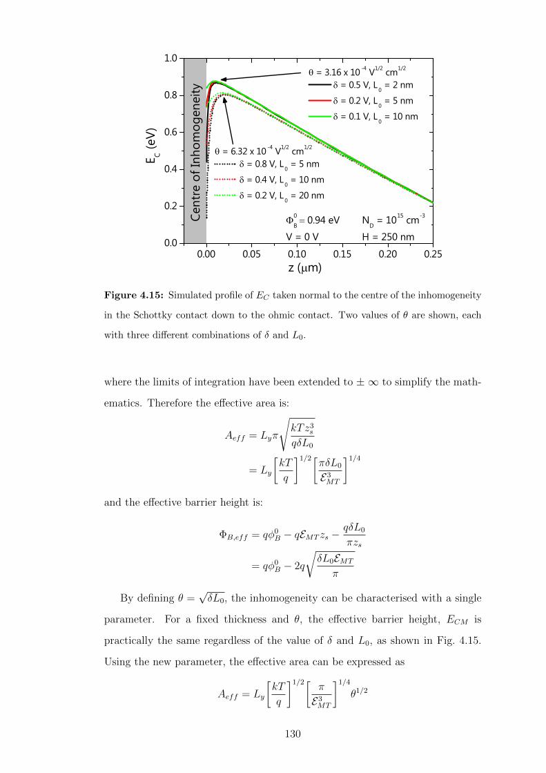
0.00 0.05 0.10 0.15 0.20 0.250.0
0.2
0.4
0.6
0.8
1.0
= 6.32 x 10 -4 V1/2 cm1/2
= 0.8 V, L0 = 5 nm
= 0.4 V, L0 = 10 nm
= 0.2 V, L0 = 20 nm
0
B0.94 eV N
D = 1015 cm-3
V = 0 V H = 250 nm
= 3.16 x 10 -4 V1/2 cm1/2
= 0.5 V, L0 = 2 nm
= 0.2 V, L0 = 5 nm
= 0.1 V, L0 = 10 nm
E C (e
V)
z ( m)
Cen
tre
of
Inho
mo
gen
eity
Figure 4.15: Simulated profile of EC taken normal to the centre of the inhomogeneity
in the Schottky contact down to the ohmic contact. Two values of θ are shown, each
with three different combinations of δ and L0.
where the limits of integration have been extended to ± ∞ to simplify the math-
ematics. Therefore the effective area is:
Aeff = Lyπ
√kTz3
s
qδL0
= Ly
[kT
q
]1/2[πδL0
E3MT
]1/4
and the effective barrier height is:
ΦB,eff = qφ0B − qEMT zs −
qδL0
πzs
= qφ0B − 2q
√δL0EMT
π
By defining θ =√δL0, the inhomogeneity can be characterised with a single
parameter. For a fixed thickness and θ, the effective barrier height, ECM is
practically the same regardless of the value of δ and L0, as shown in Fig. 4.15.
Using the new parameter, the effective area can be expressed as
Aeff = Ly
[kT
q
]1/2[π
E3MT
]1/4
θ1/2
130

and the effective barrier height becomes
ΦB,eff = qφ0B − 2qθ
√EMT
π.
When there is spatial variation of the barrier height, a distribution of θ must
be incorporated into the calculation of the current. Using a Gaussian distribution
leads to divergent integrals when calculating the current, so a Gamma distribution
with a probability density function of
P (θ) =θκ−1
Γ(κ)wκexp
(− θ
w
)θ ≥ 0
was selected instead. For ease of calculation the parameters were chosen as
w = 2ξ2/θ and κ = 3/4, giving
P (θ) =2c√θ
Γ(
34
)(2ξ2)3/4
exp
(− θ2
2ξ2
)θ ≥ 0
where ξ is a measure of the distribution width. Integrating the current over all
possible θ yields
I =
∫ ∞0
AA∗T 2 exp
−qφ0
B
kT
[exp
qV
kT
− 1
]
×
[1 +
1
Lx
[kT
q
]1/2[π
E3MT
]1/4
θ1/2 exp
2qθ√EMT
π
kT
P (θ)
]dθ
= AA∗T 2 exp
−qφ0
B
kT
[exp
qV
kT
− 1
]
×
[1 +
2c
Γ(
34
)Lx(2ξ2)3/4
[kT
q
]1/2[π
E3MT
]1/4 ∫ ∞0
θ exp
2qθ√EMT
π
kT− θ2
2ξ2
dθ
]Here, Lx is the width of the diode and c behaves as a quasi-density parameter
for low barrier regions. It has been assumed that the contribution of the higher
barrier region is small enough that their area can be assumed to be the full area
of the diode. Solving the integral and simplifying gives
I = AA∗T 2 exp
−qφ0
B
kT
[exp
qV
kT
− 1
]
×
[1 +
c
Γ(
34
)Lx
[kTξ3
q
]1/2[π3
2E3MT
]1/4
exp
(2q2ξ2EMT
πk2T 2
)].
Using this equation several of features of inhomogeneous thin-film Schottky diodes
(as discussed in Chapter 3) can be replicated. In Figs. 4.16a and b the thickness
131
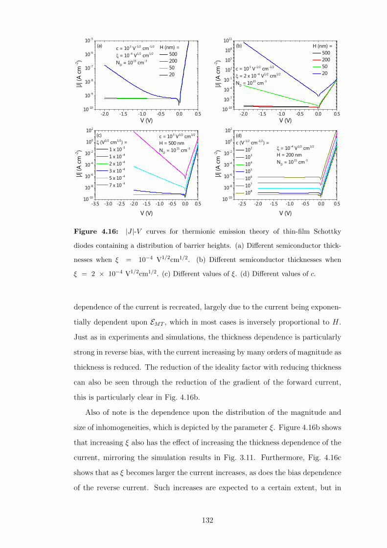
-2.0 -1.5 -1.0 -0.5 0.0 0.510-10
10-9
10-8
10-7
10-6
10-5
-2.0 -1.5 -1.0 -0.5 0.0 0.510-10
10-7
10-4
10-1
102
105
108
1011
-3.5 -3.0 -2.5 -2.0 -1.5 -1.0 -0.5 0.0 0.510-10
10-8
10-6
10-4
10-2
100
102
-2.5 -2.0 -1.5 -1.0 -0.5 0.0 0.510-10
10-8
10-6
10-4
10-2
100
102
c = 103 V-1/2 cm-1/2
= 10-4 V1/2 cm1/2
ND = 1015 cm-3
H (nm) = 500 200 50 20
(a)
|J| (A
cm
-2)
V (V)
H (nm) = 500 200 50 20
c = 103 V-1/2 cm-1/2
= 2 x 10 -4 V1/2 cm1/2
ND = 1015 cm-3
|J| (A
cm
-2)
V (V)
(b)
(c) (V1/2 cm1/2) =
1 x 10 -5
1 x 10 -4
2 x 10 -4
3 x 10 -4
5 x 10 -4
7 x 10 -4
c = 103 V1/2 cm1/2
H = 500 nmN
D = 1015 cm-3
|J| (A
cm
-2)
V (V)
(d)c (V-1/2 cm-1/2) =
102
103
104
105
106
107
108
= 10-4 V1/2 cm1/2
H = 200 nmN
D = 1015 cm-3
|J| (A
cm
-2)
V (V)
Figure 4.16: |J |-V curves for thermionic emission theory of thin-film Schottky
diodes containing a distribution of barrier heights. (a) Different semiconductor thick-
nesses when ξ = 10−4 V1/2cm1/2. (b) Different semiconductor thicknesses when
ξ = 2 × 10⁻⁴ V1/2cm1/2. (c) Different values of ξ. (d) Different values of c.
dependence of the current is recreated, largely due to the current being exponen-
tially dependent upon EMT , which in most cases is inversely proportional to H.
Just as in experiments and simulations, the thickness dependence is particularly
strong in reverse bias, with the current increasing by many orders of magnitude as
thickness is reduced. The reduction of the ideality factor with reducing thickness
can also be seen through the reduction of the gradient of the forward current,
this is particularly clear in Fig. 4.16b.
Also of note is the dependence upon the distribution of the magnitude and
size of inhomogeneities, which is depicted by the parameter ξ. Figure 4.16b shows
that increasing ξ also has the effect of increasing the thickness dependence of the
current, mirroring the simulation results in Fig. 3.11. Furthermore, Fig. 4.16c
shows that as ξ becomes larger the current increases, as does the bias dependence
of the reverse current. Such increases are expected to a certain extent, but in
132

the Fig. 4.16c the reverse current increases with increasing reverse bias without
ever saturating. This betrays a limitation of the model, namely that saddle point
in EC always exists because the dipole line approximation forces EC to tend to
negative infinity at the Schottky interface (z = 0). Finally, and perhaps most
obviously, Fig. 4.16d shows that once the contribution from the low barrier regions
dominates, the current increases linearly with the density of inhomogeneities.
4.5 Summary
For oxide semiconductors, inhomogeneities in Schottky barriers are ever present
due to various interfacial effects including oxygen deficiencies and the exposure
of different metal crystal faces. Moreover, as focus shifts towards more disor-
dered materials and cost-effective deposition methods, such as printing, barrier
inhomogeneities will become more prevalent in electronic devices incorporating
Schottky junctions.
In this chapter, a theory of homogeneous thin-film Schottky diodes was pro-
posed and was found to match the results of device simulations. Equations for the
potential within the semiconductor were derived and the effects of image force
lowering were calculated. Moreover, the effects of inhomogeneities in thin-film
Schottky diodes have been described in an analytical theory for the first time.
The thickness dependence of saddle points in the conduction band minimum,
previously seen in simulations, was faithfully reproduced by the theory and the
saddle point position was accurately predicted. Expressions for the effective bar-
rier height were also calculated and used to derive equations for current transport
over an inhomogeneous Schottky barrier. As the transport mechanism may de-
pend on the choice of materials, both thermionic emission and diffusion were
considered. An understanding of diffusion-limited transport is especially impor-
tant for disordered materials, such as those used for thin-film electronics. Current
transport across inhomogeneous Schottky barriers was modelled both in the pres-
ence and absence of a saddle point in conduction band minimum. The models
that include the saddle point demonstrate the thickness dependence of the reverse
bias seen in the Chapter 3. Moreover, the inclusion of a saddle point produces an
133

ideality factor that is dependent on thickness and inhomogeneity magnitude and
it is these circumstances that best capture the behaviour seen in the experiments.
Finally, an equation for thin-film Schottky diodes with multiple inhomogeneities
was derived, which also reproduced the trends seen in fabricated thin-film Schot-
tky diodes, including the strong thickness dependence of the reverse current and
the ideality factor.
The results presented, though limited in some ways by simplifications, offer
important insight into Schottky junctions in thin-film devices. Clear explanations
of the physical phenomena are given in the analytical models and are matched
with device simulations. Such analytical theories will be useful for the efficient
design of thin-film electronic devices as they are cheaper and less time consuming
than device simulations.
134
5 Schottky Source Transistors: Design, Theory
and Applications
Experiments and theory in this chapter were carried out in collaboration with Dr.
Jiawei Zhang. Access to simulation software was obtained with the help of Y.
Wang, M. Xu and Q. Xin.
Transistors are the bedrock of the recent technology revolutions that have shaped
the modern world. In order to drive further advancement, new transistors must
be designed to meet industry needs. One unconventional transistor design com-
bines the TFT with another fundamental component of electronics, the Schottky
diode [211]. The advantages of the resulting Schottky-source transistor (SST) in-
clude high intrinsic gain [45,99,220], low-voltage saturation [219], insensitivity to
channel length and semiconductor quality [211,236], and improved stability [242].
Within the literature, conflicting theories of device operation continue to be
proposed. For example, the gate dependence of the current has been variously
attributed to lowering of the source barrier height [223], increased tunnelling
current [99] and modulation of the effective source length [222]. There are also
differing claims about the effects of using a Schottky drain contact [99, 222].
Similarly, diode reverse current saturation [99], tunnelling [212] and depletion of
the semiconductor by the source [219] have all been suggested as causes of current
saturation. More importantly, though SSTs have been shown to have high-gain,
there remains no specific design rule for maximising the gain [99,220].
Parallel to the development of the Schottky-source transistors, breakthroughs
of oxide semiconductor devices have opened a new era in microelectronics, par-
ticularly for large-area, flexible and transparent applications [8–11]. The wide
bandgap of oxide semiconductors (typically > 3 eV) allows for high optical trans-
parency, while room-temperature processability offers compatibility with flexible
substrates. Although oxide semiconductors, particularly IGZO, are nearing ma-
turity [7,12,16,17], there remain major barriers to large-scale adoption. Foremost
among these is negative bias illumination temperature stress (NBITS) [22–30].
When IGZO TFTs are held at negative gate bias, elevated temperature and illu-
135

minated with near-bandgap energy photons there is a negative shift in the turn-on
voltage. Thus far, susceptibility to NBITS is the main factor delaying the wide-
scale adoption of IGZO as a replacement for polysilicon and amorphous silicon
in the display industry.
Of similar importance is the issue of device scaling. To maintain the rate of
improvement in electronic devices the density of transistors must be increased,
hence the size of an individual transistor must be reduced. Reducing the size of a
transistor often means reducing the length of the channel between the source and
drain contacts. Below a certain channel length, the transistor characteristics are
degraded. In the saturation regime, where transistors in displays are operated, the
current becomes dependent upon the drain bias rather than properly saturated.
Poor saturation leads to reduced intrinsic gain, as well as fluctuations in pixel
intensity in displays. IGZO TFTs suffer from these short-channel effects when
the channel length is reduced below 5 µm [31–33].
In this chapter, TFTs exhibiting extremely high intrinsic gain are designed by
adapting the new understanding of reverse-biased thin-film Schottky diodes de-
veloped in Chapters 3 and 4 [249]. Based on these designs and derived analytical
theory, an extremely high intrinsic gain of 29,000 has been achieved, which is or-
ders of magnitude higher than a conventional Si transistor. Furthermore, for the
first time, oxide semiconductor TFTs that are intrinsically impervious to NBITS
are fabricated. Moreover, these same devices show no indication of the short-
channel effect down to 360 nm. Thus, this work simultaneously maximises one
critical figure of merit and removes two major roadblocks to application. Finally,
the SST design no longer restricts the channel layer to being a semiconductor, as
demonstrated by using a semi-metal-like oxide, indium tin oxide (ITO).
5.1 Control of the Source Barrier
5.1.1 Schottky Contacts on Oxides: Important Considerations
The most important feature of the Schottky-source transistor is the barrier at
the source which controls the current. Forming a Schottky contact on an oxide
136

semiconductor is highly challenging, particularly the low homogeneous barriers
(0.3 - 0.5 eV) that are a claimed requirement for SSTs to pass sufficient cur-
rent [219, 223, 225, 231]. The formation of a good Schottky contact on an oxide
semiconductor is dependent on having sufficient oxygen content at the interface
between the metal and the semiconductor [41,122,156]. A recent study has shown
that difficultly forming Schottky barriers at Pt-IGZO interfaces is attributable
to the reduction of In3+ to In0 [157]. Unlike the diodes in Chapter 3, the need
for the SST to have a conductive channel further complicates fabrication as oxy-
gen vacancies are the donor states in oxide semiconductors [108]. Thus, having
a high source barrier and a conductive semiconductor channel are at odds with
each other, as a low oxygen concentration gives a good barrier and a resistive
channel, while a high oxygen concentration gives a poor barrier and a conduc-
tive channel. Moreover, post-annealing to improve conductivity can damage the
barrier [162], so the annealing required to produce a conductive channel must
be carried out before the deposition of the Schottky contact. Highly conductive
IGZO is easily obtained through 300 °C annealing in an N2 atmosphere, which has
been shown to reduce the density of conduction band tail states, thereby reducing
the incidence of carrier trapping and causing a corresponding improvement in the
mobility [259]. Though N2 annealing may lead to poor Schottky barriers due to
the removal of oxygen from the film, oxygen treatment may be used to restore
the barrier [41, 122, 156, 157]. Thus, to guarantee sufficient oxygen at the inter-
face, while maintaining high channel conductivity, oxygen was included during
the deposition of the Schottky contact.
5.1.2 Experimental Results for Schottky Diodes
Low temperature measurements in this subsection were carried out with the help
of Dr. Gregory Auton.
The hypothesis that high-quality Schottky contacts can be formed on conductive
oxide semiconductors by depositing the contact in an oxygen rich atmosphere was
tested by fabricating Pt-IGZO Schottky diodes. SiO2-Si wafers were cleaned by
sonic agitation in an ultrasonic bath using DECON 90, de-ionized water, acetone
137
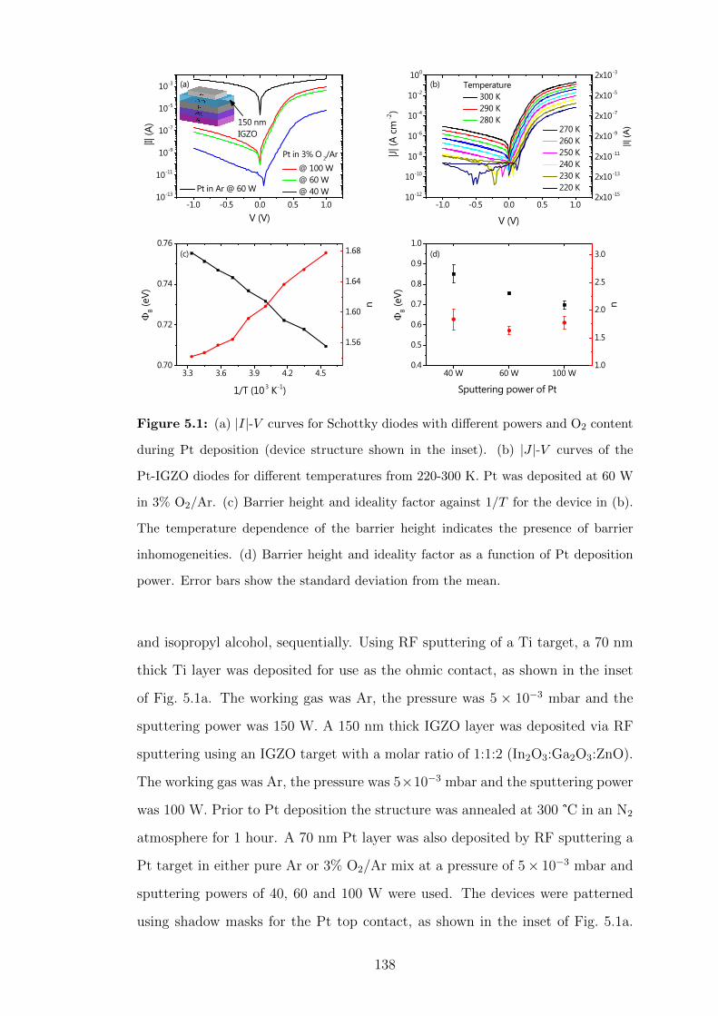
-1.0 -0.5 0.0 0.5 1.010-13
10-11
10-9
10-7
10-5
10-3
-1.0 -0.5 0.0 0.5 1.010-12
10-10
10-8
10-6
10-4
10-2
100
2x10-15
2x10-13
2x10-11
2x10⁻⁹
2x10⁻⁷
2x10⁻⁵
2x10⁻³
3.3 3.6 3.9 4.2 4.50.70
0.72
0.74
0.76
40 W 60 W 100 W0.4
0.5
0.6
0.7
0.8
0.9
1.0
Pt in Ar @ 60 W
|I| (A
)
V (V)
Pt in 3% O2/Ar
@ 100 W @ 60 W @ 40 W
150 nm IGZO
(a)
(c)
(b)
270 K 260 K 250 K 240 K 230 K 220 K
|I| (A
)
|J| (A
cm
-2)
V (V)
Temperature 300 K 290 K 280 K
B (e
V)
1/T (103 K-1)
1.56
1.60
1.64
1.68
n
(d)
Sputtering power of PtB
(eV
)
1.0
1.5
2.0
2.5
3.0
n
Figure 5.1: (a) |I|-V curves for Schottky diodes with different powers and O2 content
during Pt deposition (device structure shown in the inset). (b) |J |-V curves of the
Pt-IGZO diodes for different temperatures from 220-300 K. Pt was deposited at 60 W
in 3% O2/Ar. (c) Barrier height and ideality factor against 1/T for the device in (b).
The temperature dependence of the barrier height indicates the presence of barrier
inhomogeneities. (d) Barrier height and ideality factor as a function of Pt deposition
power. Error bars show the standard deviation from the mean.
and isopropyl alcohol, sequentially. Using RF sputtering of a Ti target, a 70 nm
thick Ti layer was deposited for use as the ohmic contact, as shown in the inset
of Fig. 5.1a. The working gas was Ar, the pressure was 5 × 10⁻³ mbar and the
sputtering power was 150 W. A 150 nm thick IGZO layer was deposited via RF
sputtering using an IGZO target with a molar ratio of 1:1:2 (In2O3:Ga2O3:ZnO).
The working gas was Ar, the pressure was 5×10⁻³ mbar and the sputtering power
was 100 W. Prior to Pt deposition the structure was annealed at 300 °C in an N2
atmosphere for 1 hour. A 70 nm Pt layer was also deposited by RF sputtering a
Pt target in either pure Ar or 3% O2/Ar mix at a pressure of 5× 10⁻³ mbar and
sputtering powers of 40, 60 and 100 W were used. The devices were patterned
using shadow masks for the Pt top contact, as shown in the inset of Fig. 5.1a.
138

Each sample contained diodes with radii of 200, 250 and 300µm.
Figure 5.1a shows the I-V curves of Pt-IGZO Schottky diodes with different
Pt deposition conditions. As expected, without oxygen treatment the Pt-IGZO
contact is effectively ohmic. To improve the oxygen content at the interface,
without affecting the conductivity of the IGZO, the Pt contacts were sputtered
in 3% O2/Ar after the thermal annealing step. Although using oxygen rich Pt as
the Schottky contact lowers the reverse current of the diodes, the reverse current
is still voltage dependent and increases with the sputtering power of Pt. For
example, when V = −1 V, the current in the 100 W diode is over two orders of
magnitude larger than in the 40 W diode.
The imperfect behaviour of the Schottky diodes is explained by the existence
of inhomogeneities in the barrier, portrayed by the high ideality factors as well
as the temperature dependence of the current and the extracted barrier height in
Figs. 5.1b and c. The low temperature measurements of IGZO Schottky diodes
were carried out using a Lakeshore cryogenic CRX-4K probe station. As the
temperature is lowered carriers can only cross the barrier in regions with lower
barrier height. These lower barrier regions may be caused by In3+ being reduced
to In0 as a result of insufficient oxygen, as well as disorder, at the interface [157].
Using oxygen rich Pt as a contact lowers the reverse current in the diode by
making the barrier more homogeneous. Varying the sputtering power also affects
the barrier inhomogeneities, as the barrier height extracted from the diode I-V
curves falls with increasing sputtering power (Fig. 5.1d). The fact that barrier
height inhomogeneities exist in all the devices is further evidenced by the strong
bias dependence of the diode reverse current [148,150,249] in Fig. 5.1a.
5.1.3 Experimental Results for SSTs
SSTs were fabricated alongside the Schottky diodes in Section 5.1.2 using SiO2-
Si wafers with the 100 nm thick SiO2 acting as the gate dielectric. The IGZO
(20 nm) and Pt (70 nm) layers were deposited using the same methods as for the
Schottky diodes and prior to Pt deposition the samples were annealed at 300 °C
in an N2 atmosphere for 1 hour. The devices were patterned using shadow masks
139
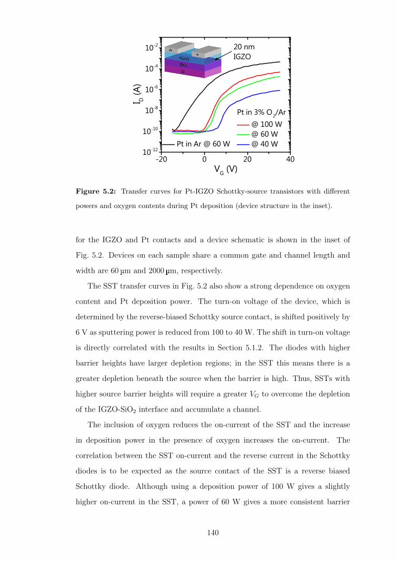
-20 0 20 4010-12
10-10
10-8
10-6
10-4
10-2
I D (A
)
VG (V)
Pt in 3% O2/Ar
@ 100 W @ 60 W @ 40 W Pt in Ar @ 60 W
20 nm IGZO
Figure 5.2: Transfer curves for Pt-IGZO Schottky-source transistors with different
powers and oxygen contents during Pt deposition (device structure in the inset).
for the IGZO and Pt contacts and a device schematic is shown in the inset of
Fig. 5.2. Devices on each sample share a common gate and channel length and
width are 60µm and 2000µm, respectively.
The SST transfer curves in Fig. 5.2 also show a strong dependence on oxygen
content and Pt deposition power. The turn-on voltage of the device, which is
determined by the reverse-biased Schottky source contact, is shifted positively by
6 V as sputtering power is reduced from 100 to 40 W. The shift in turn-on voltage
is directly correlated with the results in Section 5.1.2. The diodes with higher
barrier heights have larger depletion regions; in the SST this means there is a
greater depletion beneath the source when the barrier is high. Thus, SSTs with
higher source barrier heights will require a greater VG to overcome the depletion
of the IGZO-SiO2 interface and accumulate a channel.
The inclusion of oxygen reduces the on-current of the SST and the increase
in deposition power in the presence of oxygen increases the on-current. The
correlation between the SST on-current and the reverse current in the Schottky
diodes is to be expected as the source contact of the SST is a reverse biased
Schottky diode. Although using a deposition power of 100 W gives a slightly
higher on-current in the SST, a power of 60 W gives a more consistent barrier
140

height (see Fig. 5.1) and a turn-on voltage close to 0 V, so it was selected as the
optimal condition for Pt deposition.
5.1.4 X-Ray Photoelectron Spectroscopy of Pt Films
X-Ray Photoelectron Spectroscopy measurements were carried out by Dr. Ben
Spencer.
To understand why increasing the sputtering power of Pt in the presence of
oxygen leads to greater barrier inhomogeneities, X-ray photoelectron spectroscopy
(XPS) was carried out on Pt films deposited under different conditions. XPS
can be used for elemental analysis, i.e. finding the composition of the sample
material, in this case, the oxygen content of Pt thin-films is of interest. Three
Pt films were deposited on clean SiO2-Si wafers, one in Ar at 60 W, one in
3% O2/Ar at 60 W and one in 3% O2/Ar at 40 W. XPS only penetrates the
top 5-10 nm of the sample, so the composition results are for the surface region,
which may be different from the bulk as a result of interactions with the air or
contamination. In the case of the Pt films, this is of little concern as only the
qualitative differences between the different films are of interest, not an exact
quantitative analysis of film composition. XPS measurements were carried out
using an Axis Ultra Hybrid (Kratos, Manchester UK), run at 10 mA emission
with 15 kV bias. A charge neutraliser was used to remove any differential charging
effects. The base pressure of the instrument was 10−8 mbar. The survey scan and
the high resolution scans were run at 80 eV and 20 eV pass energies, respectively.
High resolution scans were carried out on two ranges of interest, around the O 1s
and Pt 4p3/2 peaks and the Pt 4f5/2 and 4f7/2 peaks, as well as the C 1s peak.
The analysis was carried out with CasaXPS software. The binding energies were
calibrated against the adventitious carbon peak at 284.8 eV. After calibration,
the spectra were corrected by background subtraction. The spectra were fitted
with a Gaussian-Lorentzian product formula, with the exception of Pt 4f5/2 and
4f7/2 peaks, which were fitted with a Lorentzian asymmetric line-shape.
The XPS results are shown in Fig. 5.3. When the Pt film was deposited in
an Ar atmosphere the Pt 4p3/2 peak dominates over the O 1s peak and the Pt
141
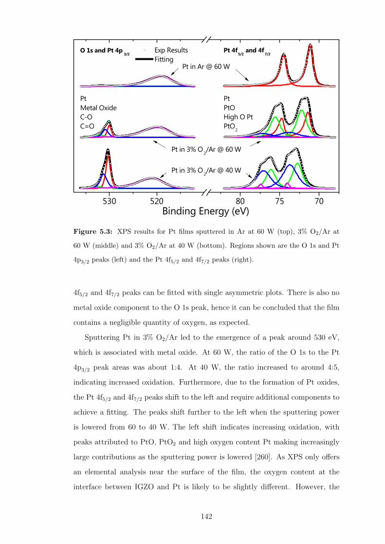
530 520 80 75 70
Exp Results Fitting
Binding Energy (eV)
O 1s and Pt 4p3/2
PtMetal OxideC-OC=O
Pt 4f5/2
and 4f7/2
PtPtOHigh O PtPtO
2
Pt in Ar @ 60 W
Pt in 3% O2/Ar @ 60 W
Pt in 3% O2/Ar @ 40 W
Figure 5.3: XPS results for Pt films sputtered in Ar at 60 W (top), 3% O2/Ar at
60 W (middle) and 3% O2/Ar at 40 W (bottom). Regions shown are the O 1s and Pt
4p3/2 peaks (left) and the Pt 4f5/2 and 4f7/2 peaks (right).
4f5/2 and 4f7/2 peaks can be fitted with single asymmetric plots. There is also no
metal oxide component to the O 1s peak, hence it can be concluded that the film
contains a negligible quantity of oxygen, as expected.
Sputtering Pt in 3% O2/Ar led to the emergence of a peak around 530 eV,
which is associated with metal oxide. At 60 W, the ratio of the O 1s to the Pt
4p3/2 peak areas was about 1:4. At 40 W, the ratio increased to around 4:5,
indicating increased oxidation. Furthermore, due to the formation of Pt oxides,
the Pt 4f5/2 and 4f7/2 peaks shift to the left and require additional components to
achieve a fitting. The peaks shift further to the left when the sputtering power
is lowered from 60 to 40 W. The left shift indicates increasing oxidation, with
peaks attributed to PtO, PtO2 and high oxygen content Pt making increasingly
large contributions as the sputtering power is lowered [260]. As XPS only offers
an elemental analysis near the surface of the film, the oxygen content at the
interface between IGZO and Pt is likely to be slightly different. However, the
142

trends established by the results can be considered trustworthy as the oxygen
content of the Pt will have a strong influence on the interfacial oxygen content.
The XPS results help to explain the effects of sputtering power and oxygen
content upon the behaviour of Schottky diodes and SSTs shown in Figs. 5.1a
and 5.2. The increased oxidation at lower sputtering power can be attributed to
the longer deposition time allowing for the inclusion of more oxygen in the film
and therefore the Pt-IGZO interface. Hence, more In3+ is reduced when higher
sputtering powers are used, leading to a greater density of lower barrier regions
and a higher reverse current in the diodes. As a result, increasing power causes
an increase in the on-current and reduction in turn-on voltage of the Schottky
source transistors.
5.2 Thickness Dependence of SST Behaviour
The study of Schottky diodes in Chapters 3 and 4 demonstrated that fully-
depleted inhomogeneous diodes have an effective barrier height that is strongly
dependent on the semiconductor thickness [249]. Given that the source barrier of
the SSTs is inhomogeneous, it may be possible to optimise the effective barrier
height of an SST by tuning the thickness of IGZO. To test this hypothesis, TFTs
and SSTs with IGZO thicknesses, H, of 20, 30 and 50 nm were simultaneously
fabricated.
The TFTs had Ti source-drain contacts deposited in Ar at a power of 150 W,
while the SSTs had Pt deposited in 3% O2/Ar at a power of 60 W. The IGZO
was deposited in pure Ar at 100 W. As would be expected, the TFTs showed
no discernible thickness dependence, as shown in Fig. 5.4a. By contrast, the
SST transfer curves in Figs. 5.4b and c show two strong thickness dependencies.
Firstly, when the drain voltage, VD, is 10 V, the turn-on voltage, VON , increases
from -18 V in the 50 nm case to 0 V in the 20 nm case. The modulation of VON
can be attributed to the ease of channel depletion by the Schottky source; for a
fixed barrier thinner semiconductors are more easily depleted, and hence require a
more positive VG to turn the channel on. Secondly, seemingly counter intuitively,
thinner devices in Fig. 5.4b have a significantly larger on-current, which is not
143

-40 -20 0 20 4010-12
10-10
10-8
10-6
10-4
10-2
-40 -20 0 20 4010-12
10-9
10-6
10-3
-40 -20 0 20 4010-12
10-9
10-6
10-3
-40 -20 0 20 40
0.0
2.0x10 -4
4.0x10 -4
6.0x10 -4
8.0x10 -4
-40 -20 0 20 40
0.0
5.0x10 -6
1.0x10 -5
1.5x10 -5
2.0x10 -5
-40 -20 0 20 40
0.0
2.0x10 -5
4.0x10 -5
6.0x10 -5
(a)V
D = 1 V
TFT
I D (A
)
VG (V)
H (nm) = 20 30 50
I D (A
)
VG (V)
(b)V
D = 1 V
Schottky source
I D (A
)
VG (V)
(c)V
D = 10 V
Schottky source
(d)V
D = 1 V
TFT
I D (A
)
VG (V)
I D (A
)
VG (V)
(e)V
D = 1 V
Schottky source
I D (A
)
VG (V)
(f)V
D = 10 V
Schottky source
Figure 5.4: Thickness dependence of IGZO TFTs displayed on log(ID)-VG at
VD = 1 V (a), SSTs at VD = 1 V (b) and SSTs at VD = 10 V (c). Corre-
sponding linear ID-VG plots are displayed in (d), (e) and (f). The devices had IGZO
thickness of 20, 30 and 50 nm. The blue arrows indicate the effect of reducing thickness
upon the turn-on voltage and the on-current.
explained by the current literature.
In Fig. 5.4d the TFTs show a linear ID-VG relationship which is typical of
TFTs in the linear regime, see Eq. 2.17. On the other hand, the SSTs in Figs. 5.4e
and f display a more complicated ID-VG relationship, which will be elucidated in
Section 5.4.
Judging by the SST output curves in Fig. 5.5, it is clear that saturation
voltage falls with semiconductor thickness, just as would be expected from the
two-dielectric model proposed by Shannon and Gerstner [219], see Section 2.4.2.
It is important to note that the saturation voltage of the SST, VDsat1, is lower
than the drain saturation voltage, VDsat2 = VG − VT , seen in ordinary TFTs.
Two trends that cannot be explained with existing knowledge are also present
in Fig. 5.5. Firstly, a thinner semiconductor gives more linear curves at low VD.
144

0 2 4 6 8 100
15
30
45
0 2 4 6 8 100
15
30
45
0 2 4 6 8 100
5
10
15
I D (
A)
VD (V)I D
(A
)VD (V)
(c) VG = 10 - 40 VH = 20 nm
(b) VG = 10 - 40 VH = 30 nm
I D (
A)
VD (V)
(a) VG = 10 - 40 V2 V per stepH = 50 nm
Figure 5.5: Output characteristics for Schottky-source transistors with 50 (a), 30 (b)
and 20 nm (c) thick IGZO layers.
It has been suggested that an exponential ID-VD relationship prior to saturation
is caused by the barrier at the drain contact [99]. However, the drain contact
is the same for all devices, as well as being forward-biased and therefore far less
resistive than the reverse-biased source. Furthermore, SST operation has already
been shown to be independent of the choice of drain contact [222].
Secondly, and critically, in the saturation region where the device is operated,
a thinner semiconductor gives a flatter, and therefore more desirable, saturation.
The flatness of saturation current is particularly important for achieving high
intrinsic gain. To investigate the origins of this sensitive thickness dependence,
device simulations were carried out.
5.3 Effects of Barrier Inhomogeneities
The behaviour of SSTs is often described using a distributed network of diodes
and resistors in the region of the source, as shown in Fig. 5.6a [222]. As the IGZO
is highly conductive and very thin, the vertical transport is likely dominated by
the reverse-biased diode at the contact rather than the vertical resistance, as
has been suggested previously [224]. All previous discussions of the operating
mechanism of SSTs have assumed a homogeneous barrier at the source contact.
145

Ohmic Contact
Gate
Drain
H
I1
I2Rint
RV
DS
ID
Source
x
z
Ohmic Contact
x
z
Gate
Dielectric
Semiconductor
Drain
L0 P
H
S
L
Dielectric
Semi-
conductor
(a) (b)
Figure 5.6: (a) Distributed diode and resistor network model for a Schottky source
transistor, proposed by Valletta et al. [222]. (b) Structure of an SST simulated using
Silvaco Atlas. The source barrier contains an inhomogeneity of width L0, shown in
yellow. The inhomogeneity is a distance P from the source edge. The semiconductor
is IGZO and is modelled on the work of Fung et al. [119], see Appendix A.1.5.
As the operating mechanism of SSTs relies so heavily upon the behaviour of the
reverse-biased Schottky barrier at the source it is important to obtain a working
knowledge of the effects of barrier height variations.
SSTs were simulated in Silvaco Atlas [250] with a barrier inhomogeneity in-
serted into the Schottky source contact, as shown in Fig. 5.6b. The barrier height
of the source was fixed as Φ0B = 0.5 eV, except at the inhomogeneity where the
barrier height was Φ0B − ∆. Only inhomogeneities with a barrier height lower
than Φ0B were considered, as higher barriers would not contribute significantly
to the current. To help understand the different contributions of the randomly
distributed inhomogeneities that occur in real contacts, the position and mag-
nitude of the inhomogeneity was varied. The value of ∆ was varied from 0, a
homogeneous source, to 0.3 eV. Inhomogeneity position with respect to the drain
end of the source edge was varied, such that P = 0, 10, 100, 1000, 4000 nm.
The inhomogeneity width was also varied L0 = 3, 10, 30 nm. Unless specified,
the source length, S, and channel length, L, were fixed such that S = 5 µm and
L = 2 µm. The IGZO thickness was varied such that H = 10, 20, 30, 50, 100 nm.
The default Atlas model for IGZO was used [119]. The dielectric was SiO2 and
the dielectric thickness was fixed at 100 nm. The length of the drain was fixed
at 1 µm and the gate overlapped the entirety of the source, drain and channel.
The channel width was fixed at 1 µm.
146

0 2 4 6 8 10-0.1
0.0
0.1
0.2
0.3
0.4
0.5
0.6
0.7
0.8
0.9
0 2 4 6 8 10
-202468
1012141618202224
VG = 0 - 10 V
I D (n
A)
VD (V)
VG = 0 - 10 V
(a) Homogeneous SourceH = 100 nm
(b) Inhomogeneous SourceH = 100 nmP = 100 nmL
0 = 10 nm
= 0.3 eV
I D (n
A)
VD (V)
Figure 5.7: Simulated output curves for an SST with a 100 nm thick IGZO layer. (a)
Device with a homogeneous source barrier. (b) Device with an inhomogeneous source
barrier. The inhomogeneity is 10 nm wide, 100 nm from the source edge and has a
magnitude of 0.3 eV.
5.3.1 Explaining the Experimental I-V Curves
Figure 5.7a shows simulated output curves of an SST with a homogeneous source
and a 100 nm thick IGZO layer. The output curve is typical of devices simulated
in the literature [222], with a low saturation current, low saturation voltage and
a high output resistance (IDsat = 0.7 nA, VDsat1 = 2.6 V and ro = 200 GΩ, when
VG = 10 V), but not an accurate representation of the experimental findings. In
Fig. 5.7b a lower barrier region (LBR, yellow region in Fig. 5.6b), with a magni-
tude ∆ = 0.3 eV, is introduced at a distance, P , of 100 nm from the drain end of
the source. The presence of the LBR leads to a large deterioration in output resis-
tance and a current increase larger than one order of magnitude. The non-linear
region seen in experiments is also replicated, suggesting that inhomogeneities are
the origin of the sub-optimal characteristics seen in Figs. 5.5a and b. Similar
behaviour can also be seen with different choices of ∆, P and L0 (not shown).
Unlike the experimental results, simulated output curves with different gate
voltages overlap prior to saturation, due to the small source length in the model.
The source length cannot be made longer as a fine mesh is required to model the
147

0 2 4 6 8 10
0.000
0.005
0.010
0.015
0.020
0.025V
G = 0 - 10 V
H = 100 nm
I D (
A)
VD (V)
Source Length = 600 m
Figure 5.8: Simulated output curves for an SST with 600 µm long homogeneous
barrier at the source.
region near the inhomogeneity and the number of nodes available is limited. The
discrepancy between simulated and experimental output curves was resolved by
simulating an SST with a homogeneous source of length S = 600 µm, which is
the same length as the fabricated devices. It is clear from the output curves in
Fig. 5.8 that when a longer source is used the output curves have a greater VG
dependence at low VD, thereby reflecting the experimental results.
The current density distribution in Fig. 5.9a shows that the current through
the device in Fig. 5.7b is dominated by the contribution from the lower barrier
region. Thus, to establish the origin of the non-linear ID-VD behaviour at low VD,
profiles of the current density across the source (shown by dashes in Fig. 5.9a)
were taken for drain voltages below saturation. Figure 5.9b shows that unlike the
rest of the source, the current through the inhomogeneity increases substantially,
by two orders of magnitude, as VD increases from 0.2 to 2 V. The origin of
the exponential growth is elucidated in Fig. 5.9c, which shows profiles of the
conduction band minimum vertically from the centre of the inhomogeneity down
to semiconductor-dielectric interface (dots in Fig. 5.9a). The profiles show that a
saddle point in EC is formed beneath the inhomogeneity and acts as an effective
barrier height for the inhomogeneity and thus the entire source. The saddle point
148
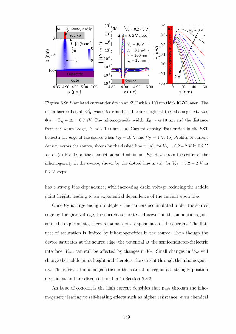
4.85 4.90 4.95 5.00 5.05
100
50
0
4.85 4.90 4.95 5.0010-4
10-3
10-2
10-1
100
101
102
103
0 20 40 60-0.2
-0.1
0.0
0.1
0.2
0.3
0.4
Profiles in (b)
Profiles in (b)
(b)
z (n
m)
x ( m)
(b)
Inhomogeneity
Source
Dielectric
Gate
|J| (A cm-2)5
0
(a)
(c)
|J| (A
cm
-2)
x ( m)
VG = 10 V
= 0.3 eVP = 100 nmL
0 = 10 nm
VD = 0.2 - 2 V
in 0.2 V steps
Source2 V
VD = 0 V
E C (e
V)
z (nm)
Inho
mog
enei
ty in
Sou
rce
(c)
Figure 5.9: Simulated current density in an SST with a 100 nm thick IGZO layer. The
mean barrier height, Φ0B, was 0.5 eV and the barrier height at the inhomogeneity was
ΦB = Φ0B − ∆ = 0.2 eV. The inhomogeneity width, L0, was 10 nm and the distance
from the source edge, P , was 100 nm. (a) Current density distribution in the SST
beneath the edge of the source when VG = 10 V and VD = 1 V. (b) Profiles of current
density across the source, shown by the dashed line in (a), for VD = 0.2− 2 V in 0.2 V
steps. (c) Profiles of the conduction band minimum, EC , down from the centre of the
inhomogeneity in the source, shown by the dotted line in (a), for VD = 0.2 − 2 V in
0.2 V steps.
has a strong bias dependence, with increasing drain voltage reducing the saddle
point height, leading to an exponential dependence of the current upon bias.
Once VD is large enough to deplete the carriers accumulated under the source
edge by the gate voltage, the current saturates. However, in the simulations, just
as in the experiments, there remains a bias dependence of the current. The flat-
ness of saturation is limited by inhomogeneities in the source. Even though the
device saturates at the source edge, the potential at the semiconductor-dielectric
interface, Vint, can still be affected by changes in VD. Small changes in Vint will
change the saddle point height and therefore the current through the inhomogene-
ity. The effects of inhomogeneities in the saturation region are strongly position
dependent and are discussed further in Section 5.3.3.
An issue of concern is the high current densities that pass through the inho-
mogeneity leading to self-heating effects such as higher resistance, even chemical
149
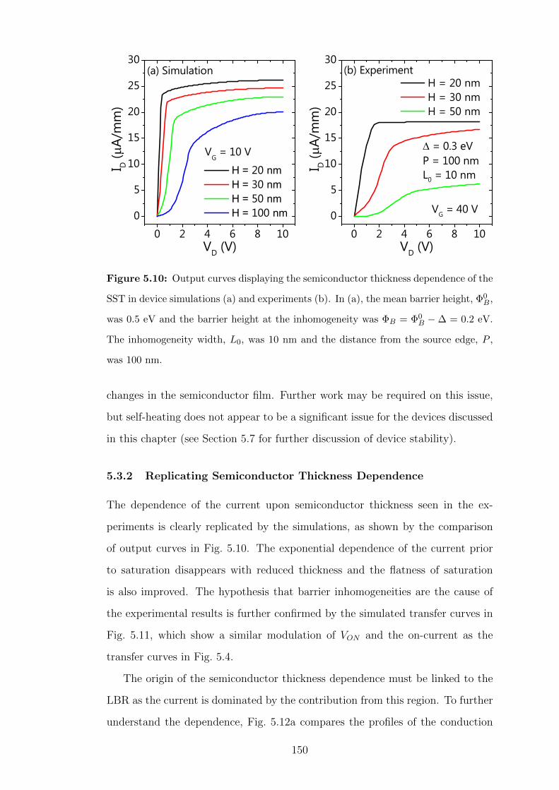
0 2 4 6 8 10
0
5
10
15
20
25
30
0 2 4 6 8 10
0
5
10
15
20
25
30(a) Simulation
= 0.3 eVP = 100 nmL0 = 10 nm
VG = 10 V
H = 20 nm H = 30 nm H = 50 nm H = 100 nm
I D (
A/m
m)
VD (V)
I D (
A/m
m)
VD (V)
H = 20 nm H = 30 nm H = 50 nm
(b) Experiment
VG = 40 V
Figure 5.10: Output curves displaying the semiconductor thickness dependence of the
SST in device simulations (a) and experiments (b). In (a), the mean barrier height, Φ0B,
was 0.5 eV and the barrier height at the inhomogeneity was ΦB = Φ0B −∆ = 0.2 eV.
The inhomogeneity width, L0, was 10 nm and the distance from the source edge, P ,
was 100 nm.
changes in the semiconductor film. Further work may be required on this issue,
but self-heating does not appear to be a significant issue for the devices discussed
in this chapter (see Section 5.7 for further discussion of device stability).
5.3.2 Replicating Semiconductor Thickness Dependence
The dependence of the current upon semiconductor thickness seen in the ex-
periments is clearly replicated by the simulations, as shown by the comparison
of output curves in Fig. 5.10. The exponential dependence of the current prior
to saturation disappears with reduced thickness and the flatness of saturation
is also improved. The hypothesis that barrier inhomogeneities are the cause of
the experimental results is further confirmed by the simulated transfer curves in
Fig. 5.11, which show a similar modulation of VON and the on-current as the
transfer curves in Fig. 5.4.
The origin of the semiconductor thickness dependence must be linked to the
LBR as the current is dominated by the contribution from this region. To further
understand the dependence, Fig. 5.12a compares the profiles of the conduction
150
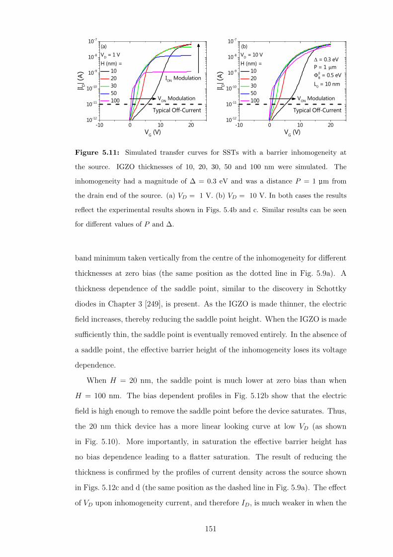
-10 0 10 2010-12
10-11
10-10
10-9
10-8
10-7
-10 0 10 2010-12
10-11
10-10
10-9
10-8
10-7
Typical Off-CurrentTypical Off-Current
ION Modulation
(b)
= 0.3 eVP = 1 m
0B = 0.5 eV
L0 = 10 nm
VD = 1 V
H (nm) = 10 20 30 50 100
|I D| (
A)
VG (V)
(a)
VON Modulation VON Modulation
VD = 10 V
H (nm) = 10 20 30 50 100
|I D| (
A)
VG (V)
Figure 5.11: Simulated transfer curves for SSTs with a barrier inhomogeneity at
the source. IGZO thicknesses of 10, 20, 30, 50 and 100 nm were simulated. The
inhomogeneity had a magnitude of ∆ = 0.3 eV and was a distance P = 1 µm from
the drain end of the source. (a) VD = 1 V. (b) VD = 10 V. In both cases the results
reflect the experimental results shown in Figs. 5.4b and c. Similar results can be seen
for different values of P and ∆.
band minimum taken vertically from the centre of the inhomogeneity for different
thicknesses at zero bias (the same position as the dotted line in Fig. 5.9a). A
thickness dependence of the saddle point, similar to the discovery in Schottky
diodes in Chapter 3 [249], is present. As the IGZO is made thinner, the electric
field increases, thereby reducing the saddle point height. When the IGZO is made
sufficiently thin, the saddle point is eventually removed entirely. In the absence of
a saddle point, the effective barrier height of the inhomogeneity loses its voltage
dependence.
When H = 20 nm, the saddle point is much lower at zero bias than when
H = 100 nm. The bias dependent profiles in Fig. 5.12b show that the electric
field is high enough to remove the saddle point before the device saturates. Thus,
the 20 nm thick device has a more linear looking curve at low VD (as shown
in Fig. 5.10). More importantly, in saturation the effective barrier height has
no bias dependence leading to a flatter saturation. The result of reducing the
thickness is confirmed by the profiles of current density across the source shown
in Figs. 5.12c and d (the same position as the dashed line in Fig. 5.9a). The effect
of VD upon inhomogeneity current, and therefore ID, is much weaker in when the
151

0.00 0.01 0.02 0.03 0.040.05
0.10
0.15
0.20
0.25
0.30
0.35
0.40
0.45
0.000 0.005 0.010 0.015 0.020-0.2
-0.1
0.0
0.1
0.2
0.3
4.885 4.890 4.895 4.900 4.905
-50
0
50
100
150
200
250
300
350
400
4.885 4.890 4.895 4.900 4.905
-50
0
50
100
150
200
250
300
350
400
100 nm
50 nm30 nm20 nm
E C (e
V)
z ( m)
0B = 0.5 eV L0 = 10 nm VD = 0 V
= 0.3 eV P = 100 nm V G = 10 V
10 nm
Inho
mog
enei
ty in
Sou
rce
(a) VD = 0 V
VG = 10 V
= 0.3 eVP = 100 nmH = 20 nmL0 = 10 nm
VD = 2 V
E C (e
V)
z ( m)
Inho
mog
enei
ty a
t So
urce
Inho
mog
enei
ty in
Sou
rce
(b)SaturationRegime
|J| (A
cm
-2)
x ( m)
H = 20 nmVG = 10 V
VD = 3 - 10 VSaturation Regime
Inhomogeneity
(c)
|J| (A
cm
-2)
x ( m)
H = 100 nmVG = 10 V
VD = 3 - 10 VSaturation Regime
Inhomogeneity
(d)
Figure 5.12: Effects of semiconductor thickness upon SST behaviour. (a) Profiles
of the conduction band minimum beneath the centre of the inhomogeneity at zero
bias for different thicknesses. A thickness dependence of the effective barrier height is
demonstrated. (b) Profiles of the conduction band minimum beneath the centre of the
inhomogeneity. The IGZO layer is 20 nm thick and VD = 0− 2 V in steps of 0.2 V. (c
and d) Profiles of current density through the inhomogeneity in the source when the
SST is saturated (VD = 3 − 10 V). The IGZO layer is 20 nm thick in (c) and 100 nm
thick in (d).
semiconductor layer is 20 nm thick as opposed to 100 nm. This is because the
absence of a saddle point means the current is determined by a linear dependence
on electric field due to diffusion, rather than an exponential dependence on the
effective barrier height. The weaker VD dependence leads to a flatter saturation,
which will improve the gain of the device and as well as its ability to operate as
a constant current source.
152

0 2 4 6 8 10
0.0
0.1
0.2
0.3
0.4
0.5
0 2 4 6 8 100
1
2
3
0 2 4 6 8 10
0
50
100
150
400 300 200 100 03
4
5
6
P (nm) = 0 10 100 1000 4000
0B 0.5 eV
VG = 10 V
L0 = 10 nm
= 0.1 eVH = 100 nm
I D (n
A)
VD (V)
(a)
I D (n
A)
VD (V)
= 0.2 eV
(b)
= 0.3 eV
I D (n
A)
VD (V)
(c)
0B 0.5 eV = 0.3 eV
P = 100 nm L0 = 10 nm
VG = 10 V H = 100 nm
Following Saturation: VD = 3 - 10 V
Vin
t (V
)Distance from source edge (nm)
Prior to Saturation: V D = 2 V
(d)
Figure 5.13: Effects of inhomogeneity position upon the characteristics of an SST with
a 100 nm thick semiconductor layer. The inhomogeneity is 10 nm wide and VG = 10 V.
(a) Output curves for ∆ = 0.1 eV. (b) Output curves for ∆ = 0.2 eV. (c) Output curves
for ∆ = 0.3 eV. (d) Potential along the semiconductor-dielectric interface beneath the
source, Vint, as a function of distance from the source edge, P , for different VD when
∆ = 0.3 eV.
5.3.3 Inhomogeneity Magnitude and Position
In a similar manner to the reverse current of the Schottky diodes, results discussed
in Section 3.2.5 and Fig. 3.11, increasing the magnitude of the inhomogeneity has
the effect of lowering the effective barrier and greatly increasing the current.
Indeed, in Figs. 5.13a, b and c increasing ∆ from 0.1 to 0.3 eV can lead to a
current increase of over two orders of magnitude when VD = VG = 10 V. For a
fixed size inhomogeneity, increasing ∆ can also lead to the formation of saddle
point, resulting in exponential regions at low VD, as can be seen by comparing
Figs. 5.13a and b.
The contribution of a lower barrier region to the current is strongly dependent
on its distance from the edge of the source nearest the drain, P . As shown in
153
the output curves in Figs. 5.13a, b and c, the nearer the inhomogeneity is to the
drain end of the source, the greater ID becomes. In Fig. 5.13c, the current grows
exponentially prior to saturation in all cases (due to the saddle point shown
in Fig. 5.9) except when the inhomogeneity is at the edge of the source, i.e.
P = 0 nm. At the edge, the inhomogeneity cannot be pinched off and no saddle
point can form in the conduction band minimum (as discussed in Section 3.4).
Under these circumstances there is no voltage dependence of the effective barrier
height and no exponential growth of current with increasing VD.
The current is so strongly dependent on the position of the lower barrier
region because of the lateral resistance beneath the source. The further from
the source edge (i.e. the greater P becomes) the lower the potential becomes
at the semiconductor-dielectric interface, as shown in Fig. 5.13d. Thus, regions
further from the source edge are less reverse-biased and so give a smaller current.
As the inhomogeneity dominates the current, the further from the source edge
it is, the lower the total current from the source. The strength of the position
dependence is highly sensitive to VG, which modulates the conductivity at the
semiconductor-dielectric interface.
Given that inhomogeneity magnitude and position have an effect on the cur-
rent, it follows that there is also an effect on the output resistance. Figures 5.14a,
b and c show how output resistance is affected by changes in ∆ and P . The sudden
increase in output resistance around VD = 2.5 V is due to source saturation and
the second steep increase between 9 and 10 V is due to the drain saturation (like
a standard TFT). For a fixed Φ0B, a larger ∆ leads to a greater difference between
the saddle point height and the barrier height at the inhomogeneity (Φ0B − ∆).
When this difference is large, the effective barrier height of the inhomogeneity
has a greater bias dependence and hence the output resistance is reduced, which
is the result in Fig. 5.14.
Figures 5.14a, b and c also show that near the source edge (P ≤ 100 nm) there
is a strong position dependence of the output resistance. Far from the source edge
(P ≥ 1 µm) the dependence of the output resistance upon inhomogeneity position
is quite weak.
154

0 2 4 6 8 10107
108
109
1010
1011
1012
1013
1014
1015
0 2 4 6 8 10 0 2 4 6 8 10
P (nm) = 0 10 100 1000 4000
r o (
)
VD (V)
(a) = 0.1 eV
VG = 10 V
L0 = 10 nm
H = 100 nm
VD (V)
(b) = 0.2 eV
VD (V)
(c) = 0.3 eV
Figure 5.14: Effects of inhomogeneity position upon the characteristics of an SST with
a 100 nm thick semiconductor layer. The inhomogeneity is 10 nm wide and VG = 10 V.
(a) Output resistance plotted against VD for ∆ = 0.1 eV. (b) Output resistance plotted
against VD for ∆ = 0.2 eV. (c) Output resistance plotted against VD for ∆ = 0.3 eV.
The origin of the strong position dependence seen when P is close to the source
edge is elucidated in Fig 5.13d. The potential profiles along the semiconductor-
dielectric interface show that when VD > VDsat1 changes in VD only affect the
potential beneath the front 200 nm or so of the source. The potential at position
x along the interface is how reverse biased the Schottky diode at the source is
at point x. Hence, when the device is saturated, only inhomogeneities within
200 nm of the source edge are exposed to changes in VD. The potential variation
beneath the front edge region can cause small variations in saddle point energy
and therefore current. It is these small current fluctuations that limit the output
resistance, and by extension the intrinsic gain, of the SST.
5.3.4 Effect of Barrier Inhomogeneities on Saturation Voltage
As low voltage saturation is one of the prominent advantages of SST behaviour,
the effect of source barrier inhomogeneities upon the saturation voltage is worthy
of consideration. Firstly, profiles of the electron concentration, ne, along the
semiconductor-dielectric interface (for ∆ = 0, 0.1, 0.2 and 0.3 eV, P = 0, 100
155

0 2 4 6
14
15
16
17
18
19
0 2 4 6 8 100
1x10¹⁸
2x10¹⁸
3x10¹⁸
4x10¹⁸
5x10¹⁸
6x10¹⁸
7x10¹⁸
8x10¹⁸
0.0 0.5 1.0 1.5 2.0 2.5 3.0
0
10
20
30
40
50
60
0.0 0.5 1.0 1.5 2.0 2.5 3.0
0.0
0.1
0.2
0.3
0.4
0.5
0.6
0.7
-0.5 0.0 0.5 1.0 1.5 2.0 2.5 3.0 3.5 4.0
0.0
0.1
0.2
0.3
0.4
0.5
0.6
0.7
0.8
0 2 4 6 8 100
1
2
3
4
5
6
VG = 10 V
P = 0 nm0B = 0.5 eV
= 0.2 eVH = 100 nmL0 = 100 nm
log(
ne)
(cm
-3)
x ( m)
VD = 0 V
VD = 10 V
(a)
Source
Min
imum
ne (
cm-3
)
VD (V)
Minima from (a) Linear Fitting
VDSAT1
(b)
I D (n
A)
VD (V)
(c)P = 0 nmVG = 0 - 10 V
H = 100 nmL
0 = 100 nm0B = 0.5 eV
= 0.2 eV = VDSAT1
(d)Homogenous Source
0B = 0.5 eV
VG = 0 - 10 V
H = 100 nm = VDSAT1
I D (n
A)
VD (V)
(e)P = 1000 nmVG = 0 - 10 V
H = 100 nmL
0 = 100 nm0B = 0.5 eV
= 0.3 eV = VDSAT1
I D (
A)
VD (V)
(f) = 0 eV = 0.1 eV = 0.2 eV = 0.3 eV
Two Dielectric ModelV D
SAT1
(V)
VG (V)
P (nm) =01001000
Figure 5.15: Effect of source barrier height inhomogeneities upon the source satura-
tion voltage of simulated SSTs with a 100 nm thick IGZO layer and a 100 nm wide
inhomogeneity. (a) Profiles of electron concentration, ne, along the semiconductor-
dielectric interface for different VD. (b) Minimum ne beneath the source edge plotted
against VD. The intercept for the linear fitting is used to estimate the source saturation
voltage, VDsat1. (c to e) Output curves for different conditions showing the accuracy of
the VDsat1 extraction method. (f) The source saturation voltage as a function of gate
voltage for different ∆ and P .
and 1000 nm, and VD and VG from 0 to 10 V when L0 and H = 100 nm) were
taken, as shown in Fig. 5.15a. When the semiconductor-dielectric interface is
depleted beneath the source edge the current should saturate, hence VDsat1 can
be considered as the VD for which ne tends to zero. Extracting the minimum
ne under the source edge for each curve and plotting it against VD allow for the
extraction of VDsat1 as the VD where ne = 0, as shown in the linear fitting in
Fig. 5.15b. It can be shown by comparing these values with output curves that
they match the actual saturation very accurately (Figs. 5.15c, d and e).
Figure 5.15f shows that for ∆ ≤ 0.2 eV there is a good fit to the two dielectric
156

model, which suggests that
∂VDsat1∂VG
=CG
CS + CG≈ 0.28 V/V
Increasing ∆ to 0.3 eV increases ∂VDsat1/∂VG to 0.35 V/V in the worst case,
which remains significantly lower than the 1 V/V expected for a TFT. These
results confirm that it is the reduced quality of saturation rather than the removal
of the mechanism itself that leads to poor device characteristics.
5.4 Analytical Theory
Besides simulations, an analytical theory can be derived to allow for further un-
derstanding of device behaviour. This theory applies for the high-gain condition
only, i.e. the effects of the saddle points can be considered negligible, due to the
semiconductor being made sufficiently thin or otherwise. In reverse bias, the
current from the source is diffusion limited [222], therefore
JV (x) ≈ qµnNCEM(x) exp
(− ΦB
kT
)[1− exp
(− qVint(x)
kT
)]where JV (x) is the vertical current density from the source at position x. At
position x, EM(x) ≈ φ0B+Vint(x)
H, where φ0
B is the mean barrier height potential
(φ0B = Φ0
B/q). Thus,
JV (x) ≈ qµnNCφ0B + Vint(x)
Hexp
(− ΦB
kT
).
When VD >> φ0B, it is assumed that the majority of current injection occurs
where Vint >> φ0B. Hence, the resistivity at position x is given by
ρV ≈VintJV≈ H
qµnNC exp
(− ΦB
kT
)Assuming that VD << (VG − VTS), where VG is the gate voltage and VTS is the
threshold voltage of the SST, then beneath the source the resistance along the
semiconductor-insulator interface is
Rint ≈1
σint=
1
qµnNint
≈ 1
µnCG(VG − VTS)
157
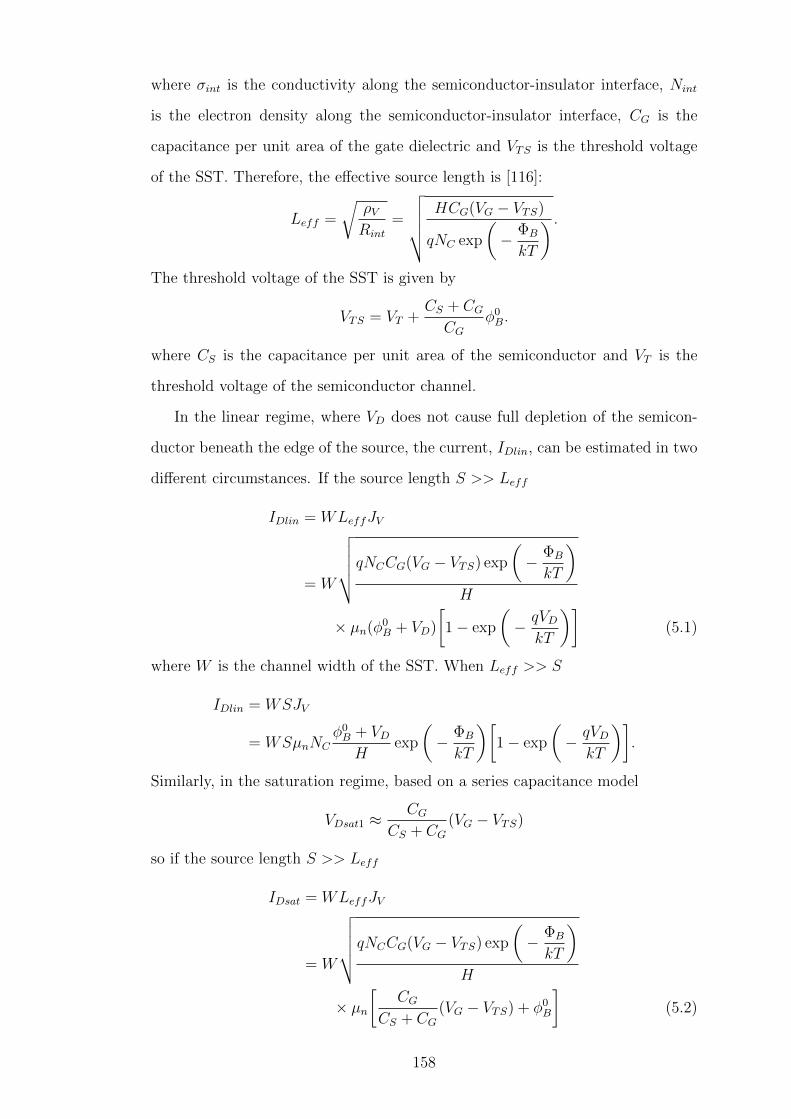
where σint is the conductivity along the semiconductor-insulator interface, Nint
is the electron density along the semiconductor-insulator interface, CG is the
capacitance per unit area of the gate dielectric and VTS is the threshold voltage
of the SST. Therefore, the effective source length is [116]:
Leff =
√ρVRint
=
√√√√√ HCG(VG − VTS)
qNC exp
(− ΦB
kT
) .The threshold voltage of the SST is given by
VTS = VT +CS + CGCG
φ0B.
where CS is the capacitance per unit area of the semiconductor and VT is the
threshold voltage of the semiconductor channel.
In the linear regime, where VD does not cause full depletion of the semicon-
ductor beneath the edge of the source, the current, IDlin, can be estimated in two
different circumstances. If the source length S >> Leff
IDlin = WLeffJV
= W
√√√√√qNCCG(VG − VTS) exp
(− ΦB
kT
)H
× µn(φ0B + VD)
[1− exp
(− qVD
kT
)](5.1)
where W is the channel width of the SST. When Leff >> S
IDlin = WSJV
= WSµnNCφ0B + VDH
exp
(− ΦB
kT
)[1− exp
(− qVD
kT
)].
Similarly, in the saturation regime, based on a series capacitance model
VDsat1 ≈CG
CS + CG(VG − VTS)
so if the source length S >> Leff
IDsat = WLeffJV
= W
√√√√√qNCCG(VG − VTS) exp
(− ΦB
kT
)H
× µn[
CGCS + CG
(VG − VTS) + φ0B
](5.2)
158

-10 0 10 20 30 4010-12
10-10
10-8
10-6
10-4
0 2 4 6 8 100
2
4
6
8
I D (A
)
VG (V)
Exp. Fitting
VD = 10 V
(a)
0
10
20
30
40
50
I D (
A)
I D (
A)
VD (V)
Exp. TheoryV
G = 20 V
VG = 26 V
VG = 30 V
(b)
Figure 5.16: Theory (Eqs. 5.3 and 5.4) and experimental data. (a) Fitting the
measured transfer curve, when VD = 10 V. (b) Fitting the measured output curves,
when VG = 20, 26 and 30 V.
and when Leff >> S
IDsat = WSJV
= WSµnNC
CGCS + CG
(VG − VTS) + φ0B
Hexp
(− ΦB
kT
)If considering image force lowering:
ΦIFL = q
√qEM
4πε0εs= q
√√√√√q
[φ0B +
(CG
CS + CG
)(VG − VTS)
]4πε0εsH
Based on recent research, the Pt-IGZO interface is not abrupt [157]. There is
a transition region where Pt clusters are encapsulated by In, which may lead to
interfacial states. Such interfacial states can lead to a barrier lowering effect with
a magnitude of αqEM [134]. Similar trends can also be attributed to tunnelling
or the electric field penetrating the metal [134]. Combining these effects, the
effective barrier at the source is
ΦB,eff = Φ0B − ΦIFL − αqEM
By substituting ΦB,eff for ΦB in the equations for IDlin and IDsat when S >> Leff
(Eqs. 5.1 and 5.2), the formulae for fitting the I-V characteristics results:
IDlin = W
√qNCCG(VG − VTS)e−ΦB,eff/kT
Hµn
(Φ0B
q+ VD
)(1− e−qVD/kT ) (5.3)
159

Parameter Type Value
Relative permittivity (εs) of
IGZO
Assumed fixed 10
Relative permittivity (εs) of
SiO2
Assumed fixed 3.9
Barrier Height (Φ0B) Taken from diode measure-
ments
0.74 eV
Conduction band effective
density of states (NC)
Assumed fixed in line with
[119]
5× 1018 cm−3
Electron mobility (µn) Taken from TFT measure-
ments
10.6 cm2/Vs
α Fitted 0.73 nm
Table 5.1: Parameters used for fitting experimental results with theory.
Similarly, in the saturation regime the current is given by:
IDsat = W
√qNCCG(VG − VTS)e−ΦB,eff/kT
Hµn
×[
CGCS + CG
(VG − VTS) +Φ0B
q
](5.4)
In the present experiment, µn = 10.6 cm2/Vs (obtained from an IGZO TFT),
W = 2 mm and the relative permittivity is 3.9 for SiO2 and 10 for IGZO. The
experimental transfer curve (circles) in Fig. 5.16a shows a very good agreement
with the values obtained from Eq. 5.4 (solid red line). The fitting also yields
α = 0.73 nm, VTS = 11.7 V and Φ0B = 0.74 eV, which agrees almost perfectly
with the results for barrier height in Fig. 5.1d. Using these same parameters,
the output curves also agreed very well with the theory (Fig. 5.16b). The above
results indicate that the analytical formulae offer an accurate description of the
I-V characteristics of an SST.
160

5.5 Intrinsic Gain
Intrinsic gain, Av, is the maximum voltage gain of a transistor. As such it is
an important measure of the ability of a TFT to amplify a signal. In display
applications, TFTs with high intrinsic gain can act as excellent constant current
sources. Furthermore, higher values of Av give greater noise margins in logic
circuits, leading to greater immunity to noise. Av can be calculated as the ratio
of transconductance, gm = ∂ID/∂VG, to output conductance, gd = ∂ID/∂VD.
As revealed in the device simulations in Section 5.3.2, the output resistance of
saturated Schottky-source transistors can be hugely improved by the removal or
near removal of saddle points in the conduction band minimum. Thus, by reduc-
ing the semiconductor thickness, the intrinsic gain can be maximised. However,
extracting the intrinsic gain directly from the I-V characteristics of the SSTs is
challenging due to the unprecedented flatness of the output curves. Such flatness
requires highly precise measurement of minute changes in ID down to the very
limit of the measurement set-up resolution. The output curves (for the SST with
20 nm thick IGZO) in Fig. 5.17a demonstrate changes in current as low as a few
picoamps over a wide range of VD from 15 to 60 V. The solid red line is a linear
fitting of the results between 15 and 60 V and the dashed lines are a guide to the
extent of the fluctuation.
Intrinsic gains of 19,000, 29,000 and 11,000 were obtained for VG = 10, 20 and
30 V, respectively, using the linear fittings in Fig. 5.17a. Using 15 point smooth-
ing (Savitzky-Golay) of the output curves, the obtained gain values have good
agreement with the linear fitting results, with some of the gain values even higher
than 100,000 at certain biases (Fig. 5.17b). To further confirm the extremely high
gain, the Schottky-source transistor was connected in an inverter set-up, using a
current source as a load (Fig. 5.17c, inset). The abrupt inversion gives a gain of
6,200, only limited by a drain compliance of 60 V.
A comparison with intrinsic gain values obtained in competing materials is
given in Fig. 5.17d [33,45,99,244,261–268]. Though a polysilicon Schottky-source
transistor was shown to have an intrinsic gain up to 10,000, this only occurred for
very narrow regions of VD, making it difficult to operate at such high gain [45].
161

0.2108
0.2110
0.2112
1.392
1.395
1.398
0 10 20 30 40 50 60
5.82
5.83
5.84
0 10 20 30 40 50 60
102
103
104
105
0
20
40
60
22 23 24 25
-6k
-4k
-2k
0
Si Organic 2D Oxide101
102
103
104
(a)
VG = 20 V
Linear fitting 500 pA
VG = 10 V
Linear fitting 50 pA
I D (
A)
VD (V)
VG = 30 V
Linear fitting 5 nA
Intr
insi
c g
ain
VD (V)
15 pt smoothing Linear fitting VG = 10 V VG = 10 V
VG = 20 V VG = 20 V
VG = 30 V VG = 30 V
(b)
VO
UT
(V)
VD-compliance
20 V 30 V 40 V 50 V 60 V
(c)
Intr
insi
c ga
in
VIN
(V)
3,2004,0005,1005,4006,200
I = 2 A
This work
ZnO [244]
IGZO [33]
IGZO [99]
Graphene [263]
Black Phosphorus [267]
MoS2 [266]
Pentacene [265]
P-13 [268]
DH4T [264]
Poly-Si [45]*
Crystalline Si [261]
Intr
insi
c g
ain
Poly-Si [262]
(d)
Figure 5.17: Intrinsic gain measurements. (a) Zoomed output curves of the Schottky-
source transistors with 20 nm thick IGZO for VG = 10, 20 and 30 V. A linear fitting of
the raw data is taken as the very small fluctuations in current fall within the tolerance
of the measurement equipment. (b) Intrinsic gain of the Schottky-source transistors
with 20 nm thick IGZO for VG = 10, 20 and 30 V. The intrinsic gain values obtained
by both the linear fitting and a 15 point smoothing of the output curves are displayed.
(c) Intrinsic gain measured using an inverter with a current source as a load. The
measurement set-up is shown in the inset. (d) A comparison of the intrinsic gain in
this work with that obtained in competing materials [33,45,99,244,261–268].
The measured Av also represents an increase of nearly two orders of magnitude
compared to other oxide semiconductors, which are significantly less mature than
polysilicon. Furthermore, there is an even larger disparity in Av between the
devices presented here and transistors made of two-dimensional materials and
organic semiconductors.
162

0 5 10 15 200 5 10 15 200 5 10 15 20
0
2
4
6
8
10
12
14(c) V
G = 16-40 V, 2 V per step(b) V
G = 16-40 V, 2 V per step
VD (V)
(a) VG = 16-40 V, 2 V per step
L = 360 nm
VD (V)
L = 602 nm
I D (
A)
VD (V)
L = 1640 nm
Figure 5.18: Output curves for short-channel Schottky contact transistors with chan-
nel lengths of 1640 nm (a), 602 nm (b) and 360 nm (c).
Such a huge improvement of the intrinsic gain would not have been possible
through understanding the operating mechanism of the SST alone. Detailed
knowledge of barrier inhomogeneities, which are especially prevalent in oxide
semiconductor Schottky junctions, is equally important. The source saturation
shields the source contact from large variations in potential and the reduced
thickness removes voltage dependent saddle points in EC beneath the LBRs.
Combined, these two factors serve to prevent small variations in VD causing large
changes in ID, thus maintaining a near constant current.
5.6 Short Channel Effect
To achieve high integration densities transistor dimensions must be scaled down.
However, the short-channel effect presents a major obstacle to such scaling. In
the case of IGZO TFTs, reducing the channel length below 5 µm produces a high
enough electric field to make the saturation current strongly dependent upon
VD [31–33]. In comparison, SSTs are more resilient to the short-channel effect
because the source region determines the current rather than the channel and its
dimensions [211, 236, 237]. Indeed, SSTs have been shown to be independent of
channel length down to 2 µm, due to the source contact being shielded from the
163

-20 0 20 4010-13
10-11
10-9
10-7
10-5
10-3
10 h 11 h 12 h 13 h 14 h 15 h 16 h 17 h 18 h 19 h 20 h
I D (A
)
VG (V)
0 h 1 h 2 h 3 h 4 h 5 h 6 h 7 h 8 h 9 h
VD = 10 V
VG-bias = -20 V
Figure 5.19: Transfer curves showing that the device behaviour under NBITS for
twenty hours. The device was exposed to heating at 60 °C, a 2000 lx white LED and
biased at VG = −20 V.
drain [211,236,237].
Using electron-beam lithography, IGZO SSTs with channel lengths of 360,
602 and 1640 nm were fabricated. The output curves in Fig. 5.18 show that flat
saturation up to VD = 20 V is maintained down to channel lengths of 360 nm.
Such immunity to the short channel effect has never been demonstrated with oxide
semiconductors. Moreover, the current is highly consistent regardless of channel
length, meaning that the SSTs are tolerant to alignment variations, which is of
great importance to large-area electronics.
5.7 Negative Bias Illumination Temperature Stress
NBITS is another long-standing barrier to the commercial application of oxide
semiconductor TFTs [22–26, 30]. Exposure to a combination of near-bandgap
illumination, negative bias and elevated temperature, as would be expected in a
display circuit, produces a negative shift in the turn-on voltage of IGZO TFTs.
The instability has been attributed to the presence of deep traps near the valence
164

band, although the exact mechanism is still not fully understood. Though sev-
eral methods have been shown to reduce the shift in VON , including high pressure
annealing [24, 28, 29] and the use of asymmetric source-drain contacts [27], it re-
mains difficult to incorporate IGZO into displays without sufficient light shielding
measures. As well as introducing an extra fabrication step, such light shielding
negates any advantages of transparency that may be offered by IGZO.
NBITS tests were carried out on 20 nm thick IGZO SSTs using an Advanced
Research Systems DE-204 temperature controlled stage. The devices were held
at VG = −20 V and 60 °C under illumination from a 2,000 lx white LED. Despite
twenty hours of stress, the device exhibited no discernible shift in VON , as shown
in Fig. 5.19. This high stability is a result of the high resistance source region
determining the current. Hence, the current is independent of the channel and
any channel instability is masked. The immunity to NBITS removes a lasting
obstruction to wide deployment of oxide semiconductors in the display industry.
5.8 Application to Other Oxide Materials
The working principle and design methodology in this work even removes the
usual restriction that the channel layer can only be a semiconductor. Here the
transparent conducting oxide ITO is tested. Except for the channel layer, ITO
SSTs were fabricated in a similar manner to the IGZO SSTs (described in Sec-
tion 5.1.3); the ITO target was sputtered in Ar, at a pressure of 5×10⁻³ mbar and
a sputtering power of 100 W. The use of such a material is difficult in ordinary
TFTs, as shown by the lack of gate modulation in the ITO TFT (Fig. 5.20a).
However, the output characteristics of an ITO SST, as shown in Fig. 5.20b, are
comparable with the IGZO SST in Fig. 5.5c. The ITO SST demonstrates that the
Schottky source contact design developed here can broaden the range of materials
used for channel layers. Furthermore, the scope of device design is extended as
using a conducting oxide as a channel layer also removes the need for a metal
drain contact.
165

-2 0 2 4 6 8 10
0
10
20
30
40
50
0 5 10 15 20
0
10
20
30
40
50
I D (m
A)
VD (V)
(a) ITO TFTH = 20 nm V
G = -10 - 40 V
5 V per step VG = 16 - 40 V
2 V per step
I D (
A)
VD (V)
(b) ITO SST
Figure 5.20: Output curves for a TFT with an ITO channel (a) and an SST with an
ITO channel (b).
5.9 Summary
By gaining a deeper understanding of the device physics of SSTs, the difficul-
ties of IGZO SST fabrication have been circumvented. Using the knowledge of
inhomogeneous thin-film Schottky diodes developed in Chapters 3 and 4 as a
starting point, the behaviour of the SST has been explained. SST behaviour was
optimised through the constructive use of barrier height inhomogeneities and the
resulting thickness dependence of the barrier height at the source. The limiting
factor of the intrinsic gain was discovered to be the bias dependent saddle points
in the conduction band minimum, formed as a result of inhomogeneities in the
source barrier. Given that it is very difficult to form the homogeneous low barri-
ers usually required for an SST using oxide semiconductors, and other disordered
materials, the mechanism of device operation proposed here is the most realistic
and accurate theory to date.
The work on Schottky diodes led to the discovery that the intrinsic gain of
the SST can be tuned by changing the semiconductor thickness. Hence, by op-
timising the thickness, an intrinsic gain of 29,000 was achieved, which represents
an unprecedented gain in thin-film transistors. Furthermore, the device design
166

means the same SSTs are able to demonstrate a remarkable robustness to reduced
channel length and excellent stability under NBITS. As such, these devices have
a huge potential for applications in large-area displays, logic gates and analogue
circuits.
Moreover, the fabrication techniques developed in this chapter are not only
applicable to IGZO, but to all n-type oxide semiconductors and even conduct-
ing oxides, such as ITO. The methods developed herein are also compatible with
complementary oxide semiconductor circuits. Indeed, the use of Pt as a con-
tact enables the use of single-step contact deposition for both n-type and p-type
transistors. More importantly, the knowledge and theory which underpin the
subsequent advantages, will be useful for all semiconductors, particularly in dis-
ordered materials.
167

6 Conclusions and Future Prospects
6.1 Conclusions
Wearable electronics and the internet-of-things promise new devices with a range
of applications from healthcare to communication. Before these life improving
technologies are realised, the limitations of conventional silicon technology, such
as its rigid form factor and lack of transparency, must be overcome. Moreover,
cost-effective mass production of such a large number of internet-enabled devices
presents a further challenge. As a result, investigations into cheaper fabrication
techniques, as well as device designs compatible with such processes, are under
way. Progress has been hastened by the development of various new materials for
thin-film electronics. Oxide semiconductors, such as IGZO, have demonstrated
many desirable characteristics including high optical transparency, compatibility
with flexible substrates and large-area uniformity. However, for thin-film electron-
ics to reach maturity there must be a firm understanding of the device physics
and the effects of using disordered materials. In this thesis, a more accurate and
complete understanding of Schottky junctions, a fundamental constituent of thin-
film electronics, was developed. The two main devices of focus were the Schottky
diode and the Schottky source transistor. Particular attention was paid to the
effects of inhomogeneous Schottky barrier height.
Firstly, by fabricating Pt-IGZO Schottky diodes, a dependence of the current
upon the thickness of the semiconductor layer was identified. This thickness de-
pendence was particularly strong in reverse bias, with the current varying over
nearly five orders of magnitude as the IGZO thickness was reduced from 250
to 50 nm. With the aid of device simulations, several potential causes of such
a dramatic dependence were ruled out including diffusion, IFL and tunnelling.
The origin of the dependence was found to be spatial variations in the Schottky
barrier height, which may be caused by disorder at the Schottky interface. When
the barrier height is inhomogeneous, lower barrier regions may be surrounded by
higher barrier regions leading to the formation of the saddle point in the conduc-
tion band minimum in the vicinity of the lower barrier region. The saddle point
168
energy acts as an effective barrier height for the diode and has a strong depen-
dence on both thickness and bias. As the semiconductor thickness is reduced, the
barrier height is lowered and, as a result, the current is exponentially increased.
Device simulations also demonstrated that thinner diodes are more sensitive to
variations in the magnitude and size of inhomogeneities. Furthermore, the be-
haviour of the saddle point explains the thickness and bias dependence of the
effective barrier height and the ideality factor. Simulations of diodes with mul-
tiple inhomogeneities can be used to explain an areal dependence of the current
density, which is observed in the literature. The combined effects of varying area
and thickness were also considered and it was found that thinner films reduce the
range of areas for which the current density is area dependent.
To further understand thin-film Schottky diodes, an analytical theory was
devised. The assumptions made in the theory of conventional Schottky diodes
are shown not to hold in thin-film devices. Using a dipole layer to approximate
a region of lower barrier height, a theory that accurately predicts the behaviour
of the saddle point in the conduction band minimum is proposed. This theory
fits well with device simulations and includes conditions for the existence of the
saddle point as well as its dependencies upon thickness and bias. By developing
a method to model the current-voltage characteristics, several special cases are
considered. Two limiting cases for current injection, thermionic emission, for
materials with high mobility, and diffusion, for materials with low mobility, are
considered in the presence and absence of a saddle point. In the absence of a
saddle point, a model with the higher and lower barrier regions conducting in
parallel is found to be sufficient to model the behaviour of the devices. When a
saddle point is present it is possible to solve the thermionic equation analytically.
However, in the diffusion limited case it is not possible to solve analytically and
a quasi-parallel model is proposed. Finally, a theory of multiple inhomogeneities
is devised by combining both the size and magnitude of an inhomogeneity into a
single parameter.
Building upon the new understanding of thin-film Schottky diodes, the Schot-
tky source transistor was considered. SSTs are a relatively new form of transistor
169

that use a Schottky, rather than ohmic, contact as the source. To achieve SST
operation the region of the source must be the dominant mechanism of current
control, thus the combination of a rectifying contact and a conducting channel
layer is required. Such a combination is difficult to achieve in oxide semiconduc-
tors, as high oxygen content is required to achieve a high, stable Schottky barrier,
but low oxygen content is required for a conductive channel. SST operation was
achieved in IGZO SSTs by annealing the IGZO film in an N2 atmosphere at
300 °C prior to depositing the Pt Schottky contacts in a 3% O2/Ar atmosphere.
During the optimisation of the SSTs a dependence of the Pt-IGZO Schottky bar-
rier height upon the sputtering power of Pt was discovered. XPS measurements
of Pt films deposited in different conditions showed that sputtering at a higher
power in 3% O2/Ar reduced the oxygen content of the film. Hence, the depen-
dence upon sputtering power can be attributed to insufficient oxygen content at
the Pt-IGZO interface. Insufficient oxygen may lead to the reduction of In3+ and
the production a greater density of lower barrier regions; resulting in the lowering
of the measured barrier height.
Device simulations were carried out to further understand the effects of barrier
height inhomogeneities in SSTs. For the first time the behaviour of an SST at
low VD is accurately explained. Moreover, it was found that the limiting factor in
the intrinsic gain of an SST is the presence of barrier height inhomogeneities near
the edge of the source (within roughly 200 nm). Just as in the Schottky diodes,
saddle points in the conduction band minimum can be formed leading to a strong
dependence of the current upon bias and semiconductor thickness. Reducing the
thickness of the semiconductor can remove the saddle points resulting in a flatter
saturation of the output characteristics. In the optimised case, where IGZO is
20 nm thick, an analytical theory was developed to fit the experimental output
curves.
Experiments were also carried out to ascertain the usefulness of the optimised
SST for application. The intrinsic gain, a key measure of amplification in any
transistor, of the IGZO SST was observed to be 29,000, a record for thin-film
transistors and roughly three orders of magnitude higher than a conventional Si
170

transistor. Due to the effective redundancy of the channel in the SST, these same
devices also show an intrinsic stability to negative bias illumination temperature
stress, one of the major bottlenecks to wider application of oxide semiconductors.
For similar reasons, it was possible to fabricate IGZO SSTs with a channel length
of 360 nm without significant degradation to performance, a record for oxide
semiconductor transistors. Such scalability of the channel length has been the
backbone of improvements in Si technology and over fifty years of Moore’s law.
Finally, by fabricating an SST with a quasi-metal indium tin oxide channel, it was
demonstrated that the SST design and fabrication techniques mentioned herein
can extend the range and versatility of materials used in thin-film transistors.
6.2 Future Prospects
In the short-term, work could focus on developing the potential of the SST. For
example, it is highly desirable to achieve operation at lower gate voltage, to
compliment the low drain voltage saturation. Such low voltage operation would
reduce the power consumption of SSTs, making them ideal for application in
low-power or battery-free wearable technology. Achieving low voltage operation
will most likely require a greater gate capacitance, brought about by changing
the material or thickness of the gate dielectric. There are several options worth
investigating, including the use of materials such as HfOx which have a high di-
electric constant, solid-state electric double layers, including a sputtered SiOx
recently developed within our research group [179], and anodised dielectrics, such
as AlxOy, which are also an area of focus within the group [21]. However, in-
creasing the gate capacitance will also increase the saturation voltage of the SST
(based on the two-dielectric model), making the optimisation of the low voltage
SST a careful balancing act.
Before the SST can be deemed suitable for applications in displays and low-
power internet-of-things devices the frequency response should be investigated.
Though some work has already been carried out in this area [227,269], the main
focus was upon theory and simulation. Obviously, the requirement of an overlap
between source and gate will limit the cut-off frequency compared to a TFT.
171
While the choice of dielectric will also be important, potentially leading to a
trade-off between cut-off frequency and power consumption.
Oxide semiconductors are also renowned for enabling flexible and transparent
electronics. Flexible SSTs are certainly a possibility, though some innovation will
be required to remove the need for high temperature annealing in N2, all the other
processing steps are compatible with flexible substrates such as PET. For IGZO
SSTs, it may be possible to replace the annealing step with Ar plasma treatment
or H2 treatment [270]. Transparent SSTs may be a more complex undertaking.
However, it has recently been shown that ITO-IGZO Schottky diodes can be fab-
ricated using multiple IGZO layers with oxygen content highest at the Schottky
interface [152]. Other techniques, such as the use of thin interfacial layers may
also be an option [151].
Changes to device and circuit architectures are also possible due to the ad-
vantages offered by the SST. For example, the use of Pt as source and drain
contacts offers the opportunity to fabricate vertically stacked devices incorporat-
ing both n-type and p-type transistors. Another example is the redundancy of
the drain contact in an ITO SST, which could be used to create more versatile
integrated circuit designs, where ITO serves as both drain contact and channel
simultaneously.
The long term influence of the work in this thesis is, like all knowledge, subject
to being superseded. The rarity of indium and gallium in the Earth’s crust make
it unlikely that IGZO is a long term solution to consumer needs [68]. Promising
work has already been carried out on multi-cation oxide semiconductors com-
prised of more abundant metals e.g. zinc tin oxide [271], but greater efforts are
required to ensure the sustainability of the thin-film electronics industry. As the
fabrication techniques developed in this thesis are applicable to all oxide semi-
conductors, adopting these indium-free materials should be relatively seamless.
Indeed, the new understanding of device physics, especially the effects of inhomo-
geneities, can be used to guide the design of Schottky diodes and SSTs regardless
of the material, thus ensuring that the work in this thesis remains relevant beyond
the short term.
172
A Device Simulation
Device simulation software is a powerful tool, which allows for the observation of
information that is difficult or impossible to measure. Further to this, simulations
may serve as an aid to optimisation, reducing the burden on experiment. In this
work, device simulations have been particularly useful in understanding the role
of inhomogeneities in Schottky barriers.
Two-dimensional (2D) physical models have been created using the technology
computer-aided design simulator tool Silvaco Atlas (version 5.14.0.R). The input
deck defining structure and physical models used in the simulation as well as the
outputs, including the bias conditions, is built in DeckBuild. The simulation is
run in Atlas, which solves semiconductor equations using the conditions specified
in the input deck. Atlas produces a runtime output, which logs the progress of
the simulation and any errors that occur. Atlas also produces log and structure
files containing the results of the simulation, both of which can be viewed in
TonyPlot.
A.1 Input Deck
A.1.1 Mesh
Firstly, a mesh must be defined for the size and structure of the device to be
mapped on to. Every grid point in the mesh is called a node and for 2D simu-
lations the total number of nodes is limited to 20,000. Discrete versions of the
equations in Section A.2 are solved iteratively at each node using a non-linear
Newton algorithm (default, others can be defined in the METHOD statement), final
solutions are obtained when the algorithm converges to within a certain tolerance.
A higher density of nodes may make for more accurate simulations, but this must
be offset against computing time and the limited allowance for nodes. Thus, it is
advisable to limit regions of dense mesh to areas where rapid changes in solutions
are expected over small distances (an example in this work is the region in the
vicinity of the barrier inhomogeneity).
173

Property Symbol Value
Relative permittivity εs 10
Bandgap EG 3.05 eV
Electron affinity χSC 4.16 eV
Conduction band effective density of states NC 5× 1018 cm−3
Valence band effective density of states NV 5× 1018 cm−3
Electron mobility µn 15 cm2/Vs
Hole mobility µp 0.1 cm2/Vs
Richardson Constant for Electrons A∗ 41 A cm−2 K−2
Table A.1: Default properties of IGZO used in Silvaco Atlas simulations.
A.1.2 Regions and Electrodes
The size and position of different material regions can be defined using the REGION
statement e.g.
region num=1 material=silicon y.min=0.0 y.max=0.05
The above example defines a region of Si from y = 0 µm to y = 0.05 µm across
the entire width (x-direction) of the mesh. Electrodes can be similarly defined
using the ELECTRODE statement.
A.1.3 Doping
Doping in different regions can be defined using the DOPING statement e.g.
doping reg=1 uniform conc=1e16 n.type
In this example the material in region 1 is uniformly n-type doped with a con-
centration ND = 1016 cm−3.
A.1.4 Material
Simulations in this thesis use the inbuilt IGZO properties (in Table A.1) derived
from the work of Fung et al. [119], unless stated otherwise.
174

Density of States
Energ
y
Conduction Band
Valence Band
Bandgap =
3.0
5 e
V
Figure A.1: Schematic of Fung’s model showing the density of states in the IGZO
bandgap.
A.1.5 Density of States
The density of states in the bandgap can be defined using the DEFECT statement.
At a specific energy, the density of states can be expressed as
N(E) = gTA(E) + gTD(E) + gGA(E) + gGD(E) (A.1)
where gTA(E) are the acceptor tails states, gTD(E) are the donor tails states,
gGA(E) are the Gaussian distributed acceptor states and gGD(E) are the Gaus-
sian distributed donor states. For the IGZO SST simulations, the model pro-
posed by Fung et al. is used [119,250], a basic schematic of the model is shown in
Fig. A.1. This model uses both donor and acceptor tail states as well as a Gaus-
sian distribution of donors to model oxygen vacancies (no Gaussian distribution
of acceptors is included). The tail states and the Gaussian distribution of donors
are modelled using the following equations:
gTA(E) = NTA exp
(E − ECWTA
); (A.2)
gTD(E) = NTD exp
(E − ECWTD
); (A.3)
gGD(E) = NGD exp
[−(E − EGDWGD
)2]. (A.4)
175

Property Symbol Value
Energy of Gaussian distributed donor
peak
EGD 2.9 eV
Total density of donor-like states in a
Gaussian distribution
NGD 6.5× 1016 cm−3 eV−1
Density of acceptor-like states in the
tail distribution at the conduction band
minimum
NTA 1.55× 1020 cm−3 eV−1
Density of donor-like states in the tail
distribution at the valence band maxi-
mum
NTD 1.55× 1020 cm−3 eV−1
Characteristic decay energy for the
Gaussian distribution of donor-like
states
WGD 0.1 eV
Characteristic decay energy for the tail
distribution of acceptor-like states
WTA 0.013 eV
Characteristic decay energy for the tail
distribution of donor-like states
WTD 0.12 eV
Table A.2: Parameters used in Silvaco Atlas simulations of SSTs to describe the
density of states in the IGZO bandgap.
The parameters input into the equations above are outlined in Table A.2.
A.1.6 Contact
Atlas automatically assumes all contacts are ohmic unless stated otherwise. To
form Schottky contacts the work function must be defined in the CONTACT state-
ment:
contact name=source workfunction=4.66 surf.rec barrier
Here, the work function of the source electrode is set to be 4.66 eV. By subtracting
the electron affinity of the semiconductor given in the MATERIAL statement, the
176
Schottky barrier height can be calculated (in this case 0.5 eV). Thermionic emis-
sion can be enabled with surf.rec, this takes the form of thermionic emission
diffusion. Incorporation of barrier lowering mechanisms using barrier causes the
following lowering term to be applied to the barrier height potential:
φBL = β
√qE
4πε0εs+ αEγ
where the first term indicates the image force lowering and the second term
can be attributed to several factors including dipole lowering, interfacial states,
tunnelling or the electric field penetrating the metal [134]. The default values are
set such that only the image force lowering term is considered (i.e. α = 0 and
β = γ = 1).
A.1.7 Models
Various physical models can be implemented in Atlas using the MODELS statement,
for example:
models print temp=300
The print parameter sends the parameters used in the simulation to the runtime
output so that they can be checked. The temp parameter sets the temperature
in Kelvin. By not defining a mobility model the low-field mobility given in the
MATERIAL statement is assumed to be constant. Atlas uses Boltzmann statistics
by default.
To model tunnelling, the universal Schottky tunnelling (UST) model may be
enabled by specifying the ust parameter on the models statement. The UST
model has localised tunnelling rates at specific nodes. This means that the cur-
vature of the conduction band is taken directly from the simulation rather than
assuming a particular shape. The tunnelling distance can also be set in Atlas,
but the default of 10 nm was used.
A.1.8 Output
The output statement allows the user to specify parameters that will be recorded
for each node throughout the device structure e.g.
177
output e.field
will map and save the electric field at each node for any structure file produced.
A.1.9 Solve
The solve statement solves the semiconductor equations at a set bias point e.g.
solve vdrain=1.0
save outf=TFT.str
solves for the whole device structure when 1 V is applied to the drain contact
and saves the structure as “TFT.str”. Producing a bias sweep on the drain from
0 to 10 V in 0.1 V steps requires the following statement:
solve name=drain vdrain=0 vfinal=10 vstep=0.1
A.1.10 DBInternal
DBInternal is a tool that allows for batches of simulations to be carried out using
two input files. The first is the template file, which is very similar to the standard
DeckBuild input deck described above. A separate design file is used to sweep
through a range of values for a certain parameter. Any parameters to be varied
must be defined as set statements at the start of the template file e.g.
set doping=6e13.
Then the actual value for the doping concentration should be replaced with
$doping e.g.
doping material=igzo uniform conc=$doping n.type
The design file loads in the template file and sweeps the chosen parameters e.g.
sweep parameter=doping type=power range="1e13, 1e17, 5"
In this case the doping is swept from 1013 to 1017 cm−3 in five steps (i.e. 1013,
1014, 1015, 1016 and 1017 cm−3).
178
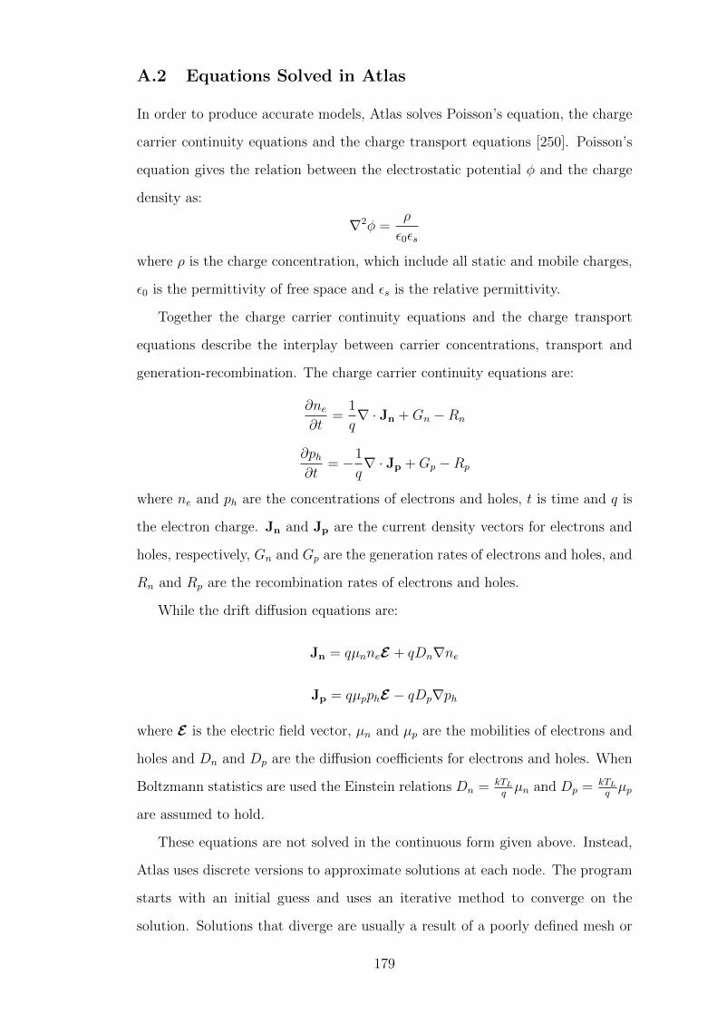
A.2 Equations Solved in Atlas
In order to produce accurate models, Atlas solves Poisson’s equation, the charge
carrier continuity equations and the charge transport equations [250]. Poisson’s
equation gives the relation between the electrostatic potential φ and the charge
density as:
∇2φ =ρ
ε0εs
where ρ is the charge concentration, which include all static and mobile charges,
ε0 is the permittivity of free space and εs is the relative permittivity.
Together the charge carrier continuity equations and the charge transport
equations describe the interplay between carrier concentrations, transport and
generation-recombination. The charge carrier continuity equations are:
∂ne∂t
=1
q∇ · Jn +Gn −Rn
∂ph∂t
= −1
q∇ · Jp +Gp −Rp
where ne and ph are the concentrations of electrons and holes, t is time and q is
the electron charge. Jn and Jp are the current density vectors for electrons and
holes, respectively, Gn and Gp are the generation rates of electrons and holes, and
Rn and Rp are the recombination rates of electrons and holes.
While the drift diffusion equations are:
Jn = qµnneE + qDn∇ne
Jp = qµpphE − qDp∇ph
where E is the electric field vector, µn and µp are the mobilities of electrons and
holes and Dn and Dp are the diffusion coefficients for electrons and holes. When
Boltzmann statistics are used the Einstein relations Dn = kTLqµn and Dp = kTL
qµp
are assumed to hold.
These equations are not solved in the continuous form given above. Instead,
Atlas uses discrete versions to approximate solutions at each node. The program
starts with an initial guess and uses an iterative method to converge on the
solution. Solutions that diverge are usually a result of a poorly defined mesh or
179

bias steps which are too large. In this work Newton’s method was used to solve
the equations.
A.3 TonyPlot
The results of the simulation, such as I-V curves or device structure files can
be viewed in TonyPlot. TonyPlot contains tools for viewing parameters such as
the electric field or electron concentrations within the device structures. One-
dimensional profiles through the device, which are used frequently throughout
this thesis, are obtained using the cutline tool. Data in TonyPlot was exported
for analysis in other programs, predominantly OriginPro.
180

References
[1] Stevenson Bacon, W. Popular Science , 124–125 November (1968).
[2] Harrop, J., Harrop, P., and Pugh, D. Technical report, IDTechEx, (2017).
[3] Das, R., Ghaffarzadeh, K., and He, X. Technical report, IDTechEx, (2017).
[4] Georgiou, T., Jalil, R., Belle, B. D., Britnell, L., Gorbachev, R. V., Moro-
zov, S. V., Kim, Y.-J., Gholinia, A., Haigh, S. J., Makarovsky, O., et al.
Nat. Nanotechnol. 8(2), 100–103 (2013).
[5] Ju, S., Facchetti, A., Xuan, Y., Liu, J., Ishikawa, F., Ye, P., Zhou, C.,
Marks, T. J., and Janes, D. B. Nat. Nanotechnol. 2(6), 378–384 (2007).
[6] Dimitrakopoulos, C. D. and Mascaro, D. J. IBM J. Res. Dev. 45(1), 11–27
(2001).
[7] Fortunato, E., Barquinha, P., and Martins, R. Adv. Mater. 24(22), 2945–
2986 (2012).
[8] Hosono, H., Kikuchi, N., Ueda, N., and Kawazoe, H. J. Non-Cryst. Solids
198, 165–169 (1996).
[9] Nomura, K., Ohta, H., Ueda, K., Kamiya, T., Hirano, M., and Hosono, H.
Science 300(5623), 1269–1272 (2003).
[10] Nomura, K., Ohta, H., Takagi, A., Kamiya, T., Hirano, M., and Hosono,
H. Nature 432(7016), 488–492 (2004).
[11] Yabuta, H., Sano, M., Abe, K., Aiba, T., Den, T., Kumomi, H., Nomura,
K., Kamiya, T., and Hosono, H. Appl. Phys. Lett. 89(11), 112123–112123
(2006).
[12] Lee, J.-H., Kim, D.-H., Yang, D.-J., Hong, S.-Y., Yoon, K.-S., Hong, P.-S.,
Jeong, C.-O., Park, H.-S., Kim, S. Y., Lim, S. K., et al. In SID Sympo-
sium Digest of Technical Papers, volume 39, 625–628. Wiley Online Library,
(2008).
181

[13] Mativenga, M., Geng, D., Kim, B., and Jang, J. ACS Appl. Mater. Inter-
faces 7(3), 1578–1585 (2015).
[14] Jung, S.-W., Koo, J. B., Park, C. W., Na, B. S., Oh, J.-Y., Lee, S. S., and
Koo, K.-W. J. Vac. Sci. Technol. B 33(5), 051201 (2015).
[15] Smith, J. T., Shah, S. S., Goryll, M., Stowell, J. R., and Allee, D. R. IEEE
Sens. J. 14(4), 937–938 (2014).
[16] Steudel, S., Steen, J.-L. P., Nag, M., Ke, T. H., Smout, S., Bel, T., Diesen,
K., Haas, G., Maas, J., Riet, J., et al. J. Soc. Inf. Display (2017).
[17] Zhang, J., Li, Y., Zhang, B., Wang, H., Xin, Q., and Song, A. Nat. Com-
mun. 6, 7561 (2015).
[18] Kamiya, T., Nomura, K., and Hosono, H. Sci. Technol. Adv. Mater. 11(4),
044305 (2010).
[19] Ofuji, M., Abe, K., Shimizu, H., Kaji, N., Hayashi, R., Sano, M., Kumomi,
H., Nomura, K., Kamiya, T., and Hosono, H. IEEE Electron Device Lett.
28(4), 273–275 (2007).
[20] Mo, Y. G., Kim, M., Kang, C. K., Jeong, J. H., Park, Y. S., Choi, C. G.,
Kim, H. D., and Kim, S. S. J. Soc. Inf. Display 19(1), 16–20 (2011).
[21] Cai, W., Park, S., Zhang, J., Wilson, J., Li, Y., Xin, Q., Majewski, L., and
Song, A. IEEE Electron Device Lett. (2018).
[22] Lee, K.-H., Jung, J. S., Son, K. S., Park, J. S., Kim, T. S., Choi, R., Jeong,
J. K., Kwon, J.-Y., Koo, B., and Lee, S. Appl. Phys. Lett. 95(23), 232106
(2009).
[23] Ryu, B., Noh, H.-K., Choi, E.-A., and Chang, K. Appl. Phys. Lett. 97(2),
022108 (2010).
[24] Ji, K. H., Kim, J.-I., Jung, H. Y., Park, S. Y., Choi, R., Kim, U. K., Hwang,
C. S., Lee, D., Hwang, H., and Jeong, J. K. Appl. Phys. Lett. 98(10), 103509
(2011).
182

[25] Oh, H., Yoon, S.-M., Ryu, M. K., Hwang, C.-S., Yang, S., and Park, S.-
H. K. Appl. Phys. Lett. 97(18), 183502 (2010).
[26] Nomura, K., Kamiya, T., Hirano, M., and Hosono, H. Appl. Phys. Lett.
95(1), 013502 (2009).
[27] Su, W.-C., Chang, T.-C., Liao, P.-Y., Chen, Y.-J., Chen, B.-W., Hsieh,
T.-Y., Yang, C.-I., Huang, Y.-Y., Chang, H.-M., Chiang, S.-C., et al. Appl.
Phys. Lett. 110(10), 103502 (2017).
[28] Seung Rim, Y., Jeong, W., Du Ahn, B., and Jae Kim, H. Appl. Phys. Lett.
102(14), 143503 (2013).
[29] Ahn, B. D., Kim, H.-S., Yun, D.-J., Park, J.-S., and Kim, H. J. ECS J.
Solid State Sci. Technol. 3(5), Q95–Q98 (2014).
[30] Chowdhury, M. D. H., Migliorato, P., and Jang, J. Appl. Phys. Lett. 97(17),
173506 (2010).
[31] Baek, G., Abe, K., Kumomi, H., and Kanicki, J. Jpn. J. Appl. Phys.
52(3S), 03BB05 (2013).
[32] Valletta, A., Fortunato, G., Mariucci, L., Barquinha, P., Martins, R., and
Fortunato, E. J. Display Technol. 10(11), 956–961 (2014).
[33] Bahubalindruni, P. G., Kiazadeh, A., Sacchetti, A., Martins, J., Rovisco,
A., Tavares, V. G., Martins, R., Fortunato, E., and Barquinha, P. J. Display
Technol. 12(6), 515–518 (2016).
[34] Lee, D. H., Nomura, K., Kamiya, T., and Hosono, H. IEEE Electron Device
Lett. 32(12), 1695–1697 (2011).
[35] Kim, H., Kim, S., Kim, K.-K., Lee, S.-N., and Ahn, K.-S. Jpn. J. Appl.
Phys. 50, 105702 (2011).
[36] Chasin, A., Steudel, S., Myny, K., Nag, M., Ke, T.-H., Schols, S., Genoe,
J., Gielen, G., and Heremans, P. Appl. Phys. Lett. 101(11), 113505 (2012).
183

[37] Chasin, A., Nag, M., Bhoolokam, A., Myny, K., Steudel, S., Schols, S.,
Genoe, J., Gielen, G., and Heremans, P. IEEE Trans. Electron Devices
60(10), 3407–3412 (2013).
[38] Zhang, J., Wang, H., Wilson, J., Ma, X., Jin, J., and Song, A. IEEE
Electron Device Lett. 37(4), 389–392 (2016).
[39] Lorenz, M., Lajn, A., Frenzel, H., Wenckstern, H. v., Grundmann, M.,
Barquinha, P., Martins, R., and Fortunato, E. Appl. Phys. Lett. 97(24),
243506 (2010).
[40] Trinh, T. T., Nguyen, V. D., Nguyen, H. H., Raja, J., Jang, J., Jang, K.,
Baek, K., Dao, V. A., and Yi, J. Appl. Phys. Lett. 100(14), 143502 (2012).
[41] Chasin, A., Zhang, L., Bhoolokam, A., Nag, M., Steudel, S., Govoreanu, B.,
Gielen, G., and Heremans, P. IEEE Electron Device Lett. 35(6), 642–644
(2014).
[42] Chasin, A., Volskiy, V., Libois, M., Myny, K., Nag, M., Rockele, M., Van-
denbosch, G. A., Genoe, J., Gielen, G., and Heremans, P. IEEE Trans.
Electron Devices 61(9), 3289–3295 (2014).
[43] Chasin, A., Volskiy, V., Libois, M., Ameys, M., Nag, M., Rockele, M.,
Myny, K., Steudel, S., Schols, S., Vandenbosch, G., et al. In International
Electronic Devices Meeting, 292–295, (2013).
[44] Xin, Q., Yan, L., Luo, Y., and Song, A. Appl. Phys. Lett. 106(11), 113506
(2015).
[45] Sporea, R., Trainor, M., Young, N., Guo, X., Shannon, J., and Silva, S.
Solid-State Electron. 65, 246–249 (2011).
[46] Badeker, K. Ann. Phys. 22, 749 (1907).
[47] Bauer, G. Ann. Phys. 422(5), 433–445 (1937).
[48] Hahn, E. E. J. Appl. Phys. 22(7), 855–863 (1951).
184

[49] Mochel, J. M. (1951). US Patent 2,564,706.
[50] Arai, T. J. Phys. Soc. Jpn. 15(5), 916–927 (1960).
[51] Klasens, H. and Koelmans, H. Solid-State Electron. 7(9), 701–702 (1964).
[52] Boesen, G. and Jacobs, J. Proc. IEEE 56(11), 2094–2095 (1968).
[53] Chopra, K., Major, S., and Pandya, D. Thin Solid Films 102(1), 1–46
(1983).
[54] Dawar, A. and Joshi, J. J. Mater. Sci. 19(1), 1–23 (1984).
[55] Bellingham, J., Phillips, W., and Adkins, C. J. Phys. Condens. Matter
2(28), 6207 (1990).
[56] Gordon, R. G. MRS Bull. 25(8), 52–57 (2000).
[57] Ellmer, K. Nat. Photonics 6(12), 809–817 (2012).
[58] Miyata, T., Hikosaka, T., and Minami, T. Sens. Actuator B-Chem. 69(1),
16–21 (2000).
[59] Aoki, A. and Sasakura, H. Jpn. J. Appl. Phys. 9(5), 582 (1970).
[60] Prins, M., Grosse-Holz, K.-O., Muller, G., Cillessen, J., Giesbers, J., Ween-
ing, R., and Wolf, R. Appl. Phys. Lett. 68(25), 3650–3652 (1996).
[61] Kawazoe, H., Yasukawa, M., Hyodo, H., Kurita, M., Yanagi, H., and
Hosono, H. Nature 389(6654), 939–942 (1997).
[62] Yao, Z., Liu, S., Zhang, L., He, B., Kumar, A., Jiang, X., Zhang, W., and
Shao, G. Appl. Phys. Lett. 101(4), 042114 (2012).
[63] Mativenga, M., Choi, M. H., Choi, J. W., and Jang, J. IEEE Electron
Device Lett. 32(2), 170–172 (2011).
[64] Ito, M., Kon, M., Miyazaki, C., Ikeda, N., Ishizaki, M., Matsubara, R.,
Ugajin, Y., and Sekine, N. Phys. Status Solidi A 205(8), 1885–1894 (2008).
185

[65] Yin, H., Kim, S., Kim, C. J., Song, I., Park, J., Kim, S., and Park, Y. Appl.
Phys. Lett. 93(17), 172109 (2008).
[66] Kamiya, T. and Hosono, H. NPG Asia Mater. 2(1), 15–22 (2010).
[67] Street, R. A. Adv. Mater. 21(20), 2007–2022 (2009).
[68] Wager, J. F., Yeh, B., Hoffman, R. L., and Keszler, D. A. Curr. Opin. Solid
State Mater. Sci. 18(2), 53–61 (2014).
[69] Matsuzaki, K., Nomura, K., Yanagi, H., Kamiya, T., Hirano, M., and
Hosono, H. Appl. Phys. Lett. 93(20), 202107–202107 (2008).
[70] Ogo, Y., Hiramatsu, H., Nomura, K., Yanagi, H., Kamiya, T., Hirano, M.,
and Hosono, H. Appl. Phys. Lett. 93(3), 032113–032113 (2008).
[71] Yabuta, H., Kaji, N., Hayashi, R., Kumomi, H., Nomura, K., Kamiya, T.,
Hirano, M., and Hosono, H. Appl. Phys. Lett. 97(7), 072111–072111 (2010).
[72] Ginley, D., Hosono, H., and Paine, D. C. Handbook of transparent conduc-
tors. Springer Science & Business Media, (2010).
[73] Fortunato, E., Barros, R., Barquinha, P., Figueiredo, V., Park, S.-H. K.,
Hwang, C.-S., and Martins, R. Appl. Phys. Lett 97(5), 052105 (2010).
[74] Fortunato, E. and Martins, R. Phys. Status Solidi Rapid Res. Lett. 5(9),
336–339 (2011).
[75] Chen, P.-C., Chiu, Y.-C., Liou, G.-L., Zheng, Z.-W., Cheng, C.-H., and
Wu, Y.-H. IEEE Electron Device Lett. 38(2), 210–212 (2017).
[76] Li, Y., Yang, J., Wang, Y., Ma, P., Yuan, Y., Zhang, J., Lin, Z., Zhou, L.,
Xin, Q., and Song, A. IEEE Electron Device Lett. 39(2), 208–211 (2018).
[77] Moezzi, A., McDonagh, A. M., and Cortie, M. B. Chem. Eng. J. 185, 1–22
(2012).
[78] Look, D. C. Mater. Sci. Eng. B 80(1), 383–387 (2001).
186
[79] Hoffman, R., Norris, B. J., and Wager, J. Appl. Phys. Lett. 82(5), 733–735
(2003).
[80] Carcia, P., McLean, R., Reilly, M., and Nunes Jr, G. Appl. Phys. Lett.
82(7), 1117–1119 (2003).
[81] Masuda, S., Kitamura, K., Okumura, Y., Miyatake, S., Tabata, H., and
Kawai, T. J. Appl. Phys. 93(3), 1624–1630 (2003).
[82] Hoffman, R. J. Appl. Phys. 95(10), 5813–5819 (2004).
[83] Park, W. I., Kim, J. S., Yi, G.-C., Bae, M., and Lee, H.-J. Appl. Phys.
Lett. 85(21), 5052–5054 (2004).
[84] Fortunato, E., Pimentel, A., Pereira, L., Goncalves, A., Lavareda, G.,
Aguas, H., Ferreira, I., Carvalho, C., and Martins, R. J. Non-Cryst. Solids
338, 806–809 (2004).
[85] Sun, J., Mourey, D. A., Zhao, D., Park, S. K., Nelson, S. F., Levy, D. H.,
Freeman, D., Cowdery-Corvan, P., Tutt, L., and Jackson, T. N. IEEE
Electron Device Lett. 29(7), 721–723 (2008).
[86] Brox-Nilsen, C., Jin, J., Luo, Y., Bao, P., and Song, A. M. IEEE Trans.
Electron Devices 60(10), 3424–3429 (2013).
[87] Jun, J. H., Park, B., Cho, K., and Kim, S. Nanotechnology 20(50), 505201
(2009).
[88] Sun, B. and Sirringhaus, H. Nano Lett. 5(12), 2408–2413 (2005).
[89] Gandla, S., Gollu, S. R., Sharma, R., Sarangi, V., and Gupta, D. Appl.
Phys. Lett. 107(15), 152102 (2015).
[90] Lin, Y.-H., Thomas, S. R., Faber, H., Li, R., McLachlan, M. A., Patsalas,
P. A., and Anthopoulos, T. D. Adv. Electron. Mater. 2(6) (2016).
[91] Hossain, F. M., Nishii, J., Takagi, S., Ohtomo, A., Fukumura, T., Fujioka,
H., Ohno, H., Koinuma, H., and Kawasaki, M. J. Appl. Phys. 94(12),
7768–7777 (2003).
187
[92] Park, W. J., Shin, H. S., Du Ahn, B., Kim, G. H., Lee, S. M., Kim, K. H.,
and Kim, H. J. Appl. Phys. Lett. 93(8), 083508 (2008).
[93] MacDonald, W. A. J. Mater. Chem. 14(1), 4–10 (2004).
[94] Staebler, D. and Wronski, C. Appl. Phys. Lett. 31(4), 292–294 (1977).
[95] Jahinuzzaman, S. M., Sultana, A., Sakariya, K., Servati, P., and Nathan,
A. Appl. Phys. Lett. 87(2), 023502 (2005).
[96] Brotherton, S. Semicond. Sci. Technol. 10(6), 721 (1995).
[97] Anthony, J. E., Facchetti, A., Heeney, M., Marder, S. R., and Zhan, X.
Adv. Mater. 22(34), 3876–3892 (2010).
[98] Sirringhaus, H. Adv. Mater. 21(38-39), 3859–3873 (2009).
[99] Lee, S. and Nathan, A. Science 354(6310), 302–304 (2016).
[100] Medvedeva, J. E., Buchholz, D. B., and Chang, R. P. Adv. Electron. Mater.
(2017).
[101] Barquinha, P., Pimentel, A., Marques, A., Pereira, L., Martins, R., and
Fortunato, E. J. Non-Cryst. Solids 352(9), 1756–1760 (2006).
[102] Chong, E., Chun, Y. S., and Lee, S. Y. Appl. Phys. Lett. 97(10), 102102
(2010).
[103] Kamiya, T., Nomura, K., and Hosono, H. J. Display Technol. 5(12), 462–
467 (2009).
[104] Gao, X., Aikawa, S., Mitoma, N., Lin, M.-F., Kizu, T., Nabatame, T., and
Tsukagoshi, K. Appl. Phys. Lett. 105(2), 023503 (2014).
[105] Kim, C.-J., Kim, S., Lee, J.-H., Park, J.-S., Kim, S., Park, J., Lee, E., Lee,
J., Park, Y., Kim, J. H., et al. Appl. Phys. Lett. 95(25), 252103 (2009).
[106] Park, J.-S., Kim, K., Park, Y.-G., Mo, Y.-G., Kim, H. D., and Jeong, J. K.
Adv. Mater. 21(3), 329–333 (2009).
188

[107] Barquinha, P., Pereira, L., Goncalves, G., Martins, R., and Fortunato, E.
J. Electrochem. Soc. 156(3), H161–H168 (2009).
[108] Hosono, H. J. Non-Cryst. Solids 352(9), 851–858 (2006).
[109] Al-Kuhaili, M., Durrani, S., and Khawaja, E. Appl. Phys. Lett. 83(22),
4533–4535 (2003).
[110] Iwasaki, T., Itagaki, N., Den, T., Kumomi, H., Nomura, K., Kamiya, T.,
and Hosono, H. Appl. Phys. Lett. 90(24), 242114 (2007).
[111] Kang, D., Song, I., Kim, C., Park, Y., Kang, T. D., Lee, H. S., Park, J.-
W., Baek, S. H., Choi, S.-H., and Lee, H. Appl. Phys. Lett. 91(9), 091910
(2007).
[112] Olziersky, A., Barquinha, P., Vila, A., Magana, C., Fortunato, E., Morante,
J., and Martins, R. Mater. Chem. Phys. 131(1), 512–518 (2011).
[113] Kamiya, T., Nomura, K., and Hosono, H. Phys. Status Solidi A 207(7),
1698–1703 (2010).
[114] Korner, W., Urban, D. F., and Elsasser, C. J. Appl. Phys. 114(16), 163704
(2013).
[115] Xiao, X., Deng, W., Chi, S., Shao, Y., He, X., Wang, L., and Zhang, S.
IEEE Trans. Electron Devices 60(12), 4159–4164 (2013).
[116] Schroder, D. K. Semiconductor Material and Device Characterization. John
Wiley & Sons Inc., New Jersey, U.S.A., 3rd edition, (2006).
[117] Park, N.-M., Kim, T.-S., and Park, S.-J. Appl. Phys. Lett. 78(17), 2575–
2577 (2001).
[118] Stewart, M., Howell, R. S., Pires, L., and Hatalis, M. K. IEEE Trans.
Electron Devices 48(5), 845–851 (2001).
[119] Fung, T.-C., Chuang, C.-S., Chen, C., Abe, K., Cottle, R., Townsend, M.,
Kumomi, H., and Kanicki, J. J. Appl. Phys. 106(8), 084511 (2009).
189

[120] Na, J. H., Kitamura, M., and Arakawa, Y. Appl. Phys. Lett. 93(6), 063501
(2008).
[121] Choi, K.-H. and Kim, H.-K. Appl. Phys. Lett. 102(5), 052103 (2013).
[122] Mosbacker, H., Strzhemechny, Y., White, B., Smith, P., Look, D. C.,
Reynolds, D., Litton, C., and Brillson, L. Appl. Phys. Lett. 87(1), 012102
(2005).
[123] U.S. Geological Survey. Mineral Commodity Summaries, (2017).
[124] Fortunato, E., Pereira, L., Barquinha, P., Botelho do Rego, A. M.,
Goncalves, G., Vila, A., Morante, J. R., and Martins, R. F. Appl. Phys.
Lett. 92(22), 222103–222103 (2008).
[125] Munck, P. S. Ann. Phys. 110(3), 437–463 (1835).
[126] Braun, F. Ann. Phys. Chem. 153, 556 (1874).
[127] Pierce, G. W. Phys. Rev. 25(1), 31 (1907).
[128] Bose, J. C. March (1904). US Patent 755,840.
[129] Schottky, W. Naturwissenschaften 26(52), 843–843 (1938).
[130] Mott, N. F. In Math. Proc. Camb. Philos. Soc., volume 34, 568–572. Cam-
bridge University Press, (1938).
[131] Schottky, W. Z. Phys. 113(5), 367–414 (1939).
[132] Bethe, H. A. MIT Radiation Lab. Rep. 43, 12 (1942).
[133] Sze, S. M. and Ng, K. K. Physics of Semiconductor Devices. John Wiley
& Sons Inc., New York, U.S.A., 3rd edition, (2006).
[134] Rhoderick, E. H. and Williams, R. H. Metal-Semiconductor Contacts,
Monographs in Electrical and Electronic Engineering No. 19. Clarendon,
Oxford, (1988).
190
[135] Grundmann, M. The Physics of Semiconductors: An Introduction Including
Devices and Nanophysics. Springer, Berlin Heidelberg, Germany, (2006).
[136] Tung, R. T. Appl. Phys. Rev. 1(1), 011304 (2014).
[137] Lajn, A., von Wenckstern, H., Grundmann, M., Wagner, G., Barquinha,
P., Fortunato, E., and Martins, R. J. Appl. Phys. 113(4), 044511 (2013).
[138] Abramowitz, M. and Stegun, I. A. Handbook of mathematical functions:
with formulas, graphs, and mathematical tables, volume 55. Courier Cor-
poration, (1964).
[139] Gaillard, N., Mariolle, D., Bertin, F., Gros-Jean, M., Proust, M., Bsiesy,
A., Bajolet, A., Chhun, S., and Djebbouri, M. Microelectron. Eng. 83(11),
2169–2174 (2006).
[140] Werner, J. H. and Guttler, H. H. J. Appl. Phys. 69(3), 1522–1533 (1991).
[141] Hsu, J., Manfra, M., Lang, D., Richter, S., Chu, S., Sergent, A., Kleiman,
R., Pfeiffer, L., and Molnar, R. Appl. Phys. Lett. 78(12), 1685–1687 (2001).
[142] Umezawa, H., Saito, T., Tokuda, N., Ogura, M., Ri, S.-G., Yoshikawa, H.,
and Shikata, S.-I. Appl. Phys. Lett. 90(7), 073506 (2007).
[143] Kim, S.-H., Kim, H.-K., and Seong, T.-Y. Appl. Phys. Lett. 86(11), 112101
(2005).
[144] Fowell, A. E., Williams, R. H., Richardson, B. E., and Shen, T.-H. Semi-
cond. Sci. Technol. 5(4), 348 (1990).
[145] Sullivan, J., Tung, R., Eaglesham, D., Schrey, F., and Graham, W. J. Vac.
Sci. Technol. B 11(4), 1564–1570 (1993).
[146] Strayer, R., Mackie, W., and Swanson, L. Surf. Sci. 34(2), 225–248 (1973).
[147] Chelvayohan, M. and Mee, C. J. Phys. C 15(10), 2305 (1982).
[148] Sullivan, J., Tung, R., Pinto, M., and Graham, W. J. Appl. Phys. 70(12),
7403–7424 (1991).
191
[149] Tung, R. Appl. Phys. Lett. 58(24), 2821–2823 (1991).
[150] Tung, R. Phys. Rev. B 45(23), 13509 (1992).
[151] Choi, M.-J., Kim, M.-H., and Choi, D.-K. Appl. Phys. Lett. 107(5), 053501
(2015).
[152] Ho, S., Yu, H., and So, F. Appl. Phys. Lett. 111(21), 212103 (2017).
[153] Semple, J., Georgiadou, D. G., Wyatt-Moon, G., Gelinck, G., and An-
thopoulos, T. D. Semicond. Sci. Technol. 32(12), 123002 (2017).
[154] Song, I., Kim, S., Yin, H., Kim, C. J., Park, J., Kim, S., Choi, H. S., Lee,
E., and Park, Y. IEEE Electron Device Lett. 29(6), 549–552 (2008).
[155] Shimura, Y., Nomura, K., Yanagi, H., Kamiya, T., Hirano, M., and Hosono,
H. Thin Solid Films 516(17), 5899–5902 (2008).
[156] Zhang, J., Xin, Q., and Song, A. J. Vac. Sci. Technol. A 34(4), 04C101
(2016).
[157] Flynn, B., Oleksak, R., Thevuthasan, S., and Herman, G. S. ACS Appl.
Mater. Interfaces (2018).
[158] Michaelson, H. B. J. Appl. Phys. 48(11), 4729–4733 (1977).
[159] Choi, K.-H. and Kim, H.-K. Appl. Phys. Lett. 102(5), 052103 (2013).
[160] Kiani, A., Hasko, D. G., Milne, W. I., and Flewitt, A. J. Appl. Phys. Lett.
102(15), 152102 (2013).
[161] Kamiya, T., Nomura, K., and Hosono, H. Appl. Phys. Lett. 96(12), 122103
(2010).
[162] Zhang, J., Zhang, L., Ma, X., Wilson, J., Jin, J., Du, L., Xin, Q., and Song,
A. Appl. Phys. Lett. 107(9), 093505 (2015).
[163] Lilienfield, J. E. U.S. Patent 1745175, (1930).
[164] Lilienfield, J. E. U.S. Patent 1877140, (1932).
192
[165] Lilienfield, J. E. U.S. Patent 1900018, (1933).
[166] Heil, O. U.K. Patent 439457, (1935).
[167] Weimer, P. K. Proc. IRE 50(6), 1462–1469 (1962).
[168] Wager, J. F., Keszler, D. A., and Presley, R. E. Transparent Electronics.
Springer, New York, U.S.A., (2008).
[169] Lee, D. H., Nomura, K., Kamiya, T., and Hosono, H. ECS Solid State Lett.
1(1), Q8–Q10 (2012).
[170] Rha, S. H., Kim, U. K., Jung, J., Kim, H. K., Jung, Y. S., Hwang, E. S.,
Chung, Y. J., Lee, M., Choi, J.-H., and Hwang, C. S. IEEE Trans. Electron
Devices 60(3), 1128–1135 (2013).
[171] Suresh, A., Wellenius, P., Dhawan, A., and Muth, J. Appl. Phys. Lett.
90(12), 123512 (2007).
[172] Nomura, K., Kamiya, T., Ohta, H., Hirano, M., and Hosono, H. Appl.
Phys. Lett. 93(19), 192107–192107 (2008).
[173] Wilk, G. D., Wallace, R. M., and Anthony, J. J. Appl. Phys. 89(10), 5243–
5275 (2001).
[174] Barquinha, P., Pereira, L., Goncalves, G., Martins, R., Fortunato, E.,
Kuscer, D., Kosec, M., Vila, A., Olziersky, A., and Morante, J. R. J.
Soc. Inf. Display 18(10), 762–772 (2010).
[175] Pereira, L., Barquinha, P., Goncalves, G., Vila, A., Olziersky, A., Morante,
J., Fortunato, E., and Martins, R. Phys. Status Solidi A 206(9), 2149–2154
(2009).
[176] Pei, Z., Pereira, L., Goncalves, G., Barquinha, P., Franco, N., Alves, E.,
Rego, A., Martins, R., and Fortunato, E. Electrochem. Solid State Lett.
12(10), G65–G68 (2009).
[177] Jiang, J., Wan, Q., Sun, J., and Lu, A. Appl. Phys. Lett. 95(15), 2114
(2009).
193
[178] Xiao, H., Zhu, L. Q., Liu, Y. H., and Liu, R. RSC Adv. 6(2), 1053–1057
(2016).
[179] Ma, X., Zhang, J., Cai, W., Wang, H., Wilson, J., Wang, Q., Xin, Q., and
Song, A. Sci. Rep. 7 (2017).
[180] Cai, W., Zhang, J., Wilson, J., Ma, X., Wang, H., Zhang, X., Xin, Q., and
Song, A. IEEE Electron Device Lett. 38(12), 1680–1683 (2017).
[181] Kim, W.-S., Moon, Y.-K., Kim, K.-T., Lee, J.-H., and Park, J.-W. Thin
Solid Films 518(22), 6357–6360 (2010).
[182] Rha, S. H., Jung, J., Jung, Y., Chung, Y. J., Kim, U. K., Hwang, E. S.,
Park, B. K., Park, T. J., Choi, J.-H., and Hwang, C. S. IEEE Trans.
Electron Devices 59(12), 3357–3363 (2012).
[183] Conley, J. F. IEEE Trans. Device Mater. Rel. 10(4), 460–475 (2010).
[184] Park, J., Kim, S., Kim, C., Kim, S., Song, I., Yin, H., Kim, K.-K., Lee, S.,
Hong, K., Lee, J., et al. Appl. Phys. Lett. 93(5), 053505–053505 (2008).
[185] Jeong, J. K., Yang, H. W., Jeong, J. H., Mo, Y.-G., and Kim, H. D. Appl.
Phys. Lett. 93(12), 123508 (2008).
[186] Sato, A., Abe, K., Hayashi, R., Kumomi, H., Nomura, K., Kamiya, T., Hi-
rano, M., and Hosono, H. Appl. Phys. Lett. 94(13), 133502–133502 (2009).
[187] Choi, S.-H., Jang, J.-H., Kim, J.-J., and Han, M.-K. IEEE Electron Device
Lett. 33(3), 381–383 (2012).
[188] Martins, R., Nathan, A., Barros, R., Pereira, L., Barquinha, P., Correia,
N., Costa, R., Ahnood, A., Ferreira, I., and Fortunato, E. Adv. Mater.
23(39), 4491–4496 (2011).
[189] Lee, G. J., Kim, J., Kim, J.-H., Jeong, S. M., Jang, J. E., and Jeong, J.
Semicond. Sci. Technol. 29(3), 035003 (2014).
194

[190] Lee, H.-N., Kyung, J., Sung, M.-C., Kim, D. Y., Kang, S. K., Kim, S.-J.,
Kim, C. N., Kim, H.-G., and Kim, S.-T. J. Soc. Inf. Display 16(2), 265–272
(2008).
[191] Park, M.-J., Yun, D.-J., Ryu, M.-K., Yang, J.-H., Pi, J.-E., Kwon, O.-S.,
Kim, G. H., Hwang, C.-S., Bak, J.-Y., and Yoon, S.-M. J. Mater. Chem.
C 3(18), 4779–4786 (2015).
[192] He, Y., Wang, X., Gao, Y., Hou, Y., and Wan, Q. J. Semicond. 39(1),
011005 (2018).
[193] Zan, H.-W., Li, C.-H., Yeh, C.-C., Dai, M.-Z., Meng, H.-F., and Tsai, C.-C.
Appl. Phys Lett. 98(25), 253503 (2011).
[194] Lujan, R. and Street, R. IEEE Electron Device Lett. 33(5), 688–690 (2012).
[195] Suresh, A., Novak, S., Wellenius, P., Misra, V., and Muth, J. F. Appl.
Phys. Lett. 94(12), 123501 (2009).
[196] Munzenrieder, N., Petti, L., Zysset, C., Salvatore, G. A., Kinkeldei, T.,
Perumal, C., Carta, C., Ellinger, F., and Troster, G. In International
Electronic Devices Meeting, 5–2. IEEE, (2012).
[197] Dindar, A., Kim, J., Fuentes-Hernandez, C., and Kippelen, B. Appl. Phys.
Lett. 99(17), 172104 (2011).
[198] Nomura, K. In SID Symposium Digest of Technical Papers, volume 46,
591–594. Wiley Online Library, (2015).
[199] Sunamura, H., Kaneko, K., Furutake, N., Saito, S., Narihiro, M., Hane,
M., and Hayashi, Y. In VLSI Technology (VLSIT), 2013 Symposium on,
T250–T251. IEEE, (2013).
[200] Zhang, J., Yang, J., Li, Y., Wilson, J., Ma, X., Xin, Q., and Song, A.
Materials 10(3), 319 (2017).
[201] Yang, J., Wang, Y., Li, Y., Yuan, Y., Hu, Z., Ma, P., Zhou, L., Wang, Q.,
Song, A., and Xin, Q. IEEE Electron Device Lett. (2018).
195

[202] Kimura, M., Koga, Y., Nakanishi, H., Matsuda, T., Kameda, T., and
Nakashima, Y. IEEE J. Electron Dev. Soc. 6(1), 100–105 (2018).
[203] Ghaffarzadeh, K. and Das, R. Technical report, IDTechEx, (2014).
[204] Taken from http://www.samsung.com/us/news/newsRead.do?news seq=19836
on 20/03/2015., (2011).
[205] Soneira, R. M. Taken from http://www.displaymate.com/Tablet ShootOut 3.htm
on 23/01/18, (2013).
[206] Guillaume Chansin, K. G. and Zervos, H. Technical report, IDTechEx,
(2016).
[207] Yamaguchi, H., Ueda, T., Miura, K., Saito, N., Nakano, S., Sakano, T.,
Sugi, K., Amemiya, I., Hiramatsu, M., and Ishida, A. In SID Symposium
Digest of Technical Papers, volume 43, 1002–1005. Wiley Online Library,
(2012).
[208] Thomas, G. Nature 389(6654), 907–908 (1997).
[209] Hisamoto, D., Lee, W.-C., Kedzierski, J., Takeuchi, H., Asano, K., Kuo,
C., Anderson, E., King, T.-J., Bokor, J., and Hu, C. IEEE Trans. Electron
Devices 47(12), 2320–2325 (2000).
[210] Bardeen, J. and Brattain, W. H. Phys. Rev. 74(2), 230 (1948).
[211] Shannon, J. and Gerstner, E. IEEE Electron Device Lett. 24(6), 405–407
(2003).
[212] Wang, L., Sun, Y., Zhang, X., Zhang, L., Zhang, S., and Chan, M. Appl.
Phys. Lett. 110(15), 152105 (2017).
[213] Lepselter, M. P. and Sze, S. M. Proc. IEEE 56(8), 1400–1402 (1968).
[214] Connelly, D., Faulkner, C., and Grupp, D. E. IEEE Trans. Electron Devices
50(5), 1340–1345 (2003).
[215] Dubois, E. and Larrieu, G. J. Appl. Phys. 96(1), 729–737 (2004).
196
[216] Larson, J. M. and Snyder, J. P. IEEE Trans. Electron Devices 53(5), 1048–
1058 (2006).
[217] Qiu, Z., Zhang, Z., Ostling, M., and Zhang, S.-L. IEEE Trans. Electron
Devices 55(1), 396–403 (2008).
[218] Knoch, J. and Appenzeller, J. Appl. Phys. Lett. 81(16), 3082–3084 (2002).
[219] Shannon, J. and Gerstner, E. Solid-State Electron. 48(7), 1155–1161 (2004).
[220] Sporea, R. A., Trainor, M. J., Young, N. D., Shannon, J. M., and Silva, S.
R. P. IEEE Trans. Electron Devices 57(10), 2434–2439 (2010).
[221] Adl, A. H., Ma, A., Gupta, M., Benlamri, M., Tsui, Y. Y., Barlage, D. W.,
and Shankar, K. ACS Appl. Mater. Interfaces 4(3), 1423–1428 (2012).
[222] Valletta, A., Mariucci, L., Rapisarda, M., and Fortunato, G. J. Appl. Phys.
114(6), 064501 (2013).
[223] Shannon, J. M., Sporea, R. A., Georgakopoulos, S., Shkunov, M., and Silva,
S. R. P. IEEE Trans. Electron Devices 60(8), 2444–2449 (2013).
[224] Sporea, R. A. and Silva, S. R. P. In Proceedings of the International Semi-
conductor Conference (CAS), 155–158. IEEE, (2017).
[225] Sporea, R., Trainor, M., Young, N., Shannon, J., and Silva, S. Sci. Rep. 4
(2014).
[226] Sporea, R., Overy, M., Shannon, J., and Silva, S. J. Appl. Phys. 117(18),
184502 (2015).
[227] Shannon, J. M. and Balon, F. IEEE Trans. Electron Devices 56(10), 2354–
2356 (2009).
[228] Balon, F. and Shannon, J. J. Electrochem. Soc. 152(8), G674–G677 (2005).
[229] Sporea, R. A., Guo, X., Shannon, J., and Silva, S. In Proceedings of the
International Semiconductor Conference (CAS), volume 2, 413–416, (2009).
197

[230] Chen, C., Abe, K., Kumomi, H., and Kanicki, J. IEEE Trans. Electron
Devices 56(6), 1177–1183 (2009).
[231] Sporea, R. A., Burridge, T., and Silva, S. R. P. Sci. Rep. 5, 14058 (2015).
[232] Sporea, R. A., Trainor, M. J., Young, N. D., Shannon, J. M., and Silva, S.
R. P. IEEE Trans. Electron Devices 59(8), 2180–2186 (2012).
[233] Xu, X., Sporea, R. A., and Guo, X. J. Display Technol. 10(11), 928–933
(2014).
[234] Larson, J. M. and Snyder, J. P. IEEE Trans. Electron Devices 53(5), 1048–
1058 (2006).
[235] Huang, H.-Y., Wang, S.-J., Wu, C.-H., Chiang, C.-K., and Su, J.-Y. Appl.
Phys. Lett. 102(9), 092108 (2013).
[236] Shannon, J., Dovinos, D., Balon, F., Glasse, C., and Brotherton, S. IEEE
Electron Device Lett. 26(10), 734–736 (2005).
[237] Ma, A. M., Gupta, M., Afshar, A., Shoute, G., Tsui, Y. Y., Cadien, K. C.,
and Barlage, D. W. Appl. Phys. Lett. 103(25), 253503 (2013).
[238] Lindner, T., Paasch, G., and Scheinert, S. IEEE Trans. Electron Devices
52(1), 47–55 (2005).
[239] Balon, F., Shannon, J. M., and Sealy, B. J. Appl. Phys. Lett. 86(7), 073503
(2005).
[240] Okamura, K., Nasr, B., Brand, R. A., and Hahn, H. J. Mater. Chem.
22(11), 4607–4610 (2012).
[241] Ko, S. H., Pan, H., Grigoropoulos, C. P., Luscombe, C. K., Frechet, J. M.,
and Poulikakos, D. Nanotechnology 18(34), 345202 (2007).
[242] Shannon, J. Appl. Phys. Lett. 85(2), 326–328 (2004).
[243] Ma, A. M., Gupta, M., Chowdhury, F. R., Shen, M., Bothe, K., Shankar,
K., Tsui, Y., and Barlage, D. W. Solid-State Electron. 76, 104–108 (2012).
198

[244] Dahiya, A., Opoku, C., Sporea, R., Sarvankumar, B., Poulin-Vittrant, G.,
Cayrel, F., Camara, N., and Alquier, D. Sci. Rep. 6 (2016).
[245] Opoku, C., Dahiya, A. S., Poulin-Vittrant, G., Camara, N., and Alquier,
D. Phys. Status Solidi A (2016).
[246] Mariucci, L., Rapisarda, M., Valletta, A., Jacob, S., Benwadih, M., and
Fortunato, G. Org. Electronics 14(1), 86–93 (2013).
[247] Jacunski, M. D., Shur, M. S., Owusu, A. A., Ytterdal, T., Hack, M., and
Iniguez, B. IEEE Trans. Electron Devices 46(6), 1146–1158 (1999).
[248] Valletta, A., Gaucci, P., Mariucci, L., Fortunato, G., and Brotherton, S.
Appl. Phys. Lett. 85(15), 3113–3115 (2004).
[249] Wilson, J., Zhang, J., Li, Y., Wang, Y., Xin, Q., and Song, A. Appl. Phys.
Lett. 111(21), 213503 (2017).
[250] Silvaco, Inc. Atlas User’s Manual, (2016).
[251] Takagi, A., Nomura, K., Ohta, H., Yanagi, H., Kamiya, T., Hirano, M.,
and Hosono, H. Thin Solid Films 486(1), 38–41 (2005).
[252] Du, L., Li, H., Yan, L., Zhang, J., Xin, Q., Wang, Q., and Song, A. Appl.
Phys. Lett. 110(1), 011602 (2017).
[253] Smoluchowski, R. Phys. Rev. 60(9), 661 (1941).
[254] Skriver, H. L. and Rosengaard, N. Phys. Rev. B 46(11), 7157 (1992).
[255] Waldrop, J. R. Appl. Phys. Lett. 44(10), 1002–1004 (1984).
[256] Smit, G., Rogge, S., and Klapwijk, T. Appl. Phys. Lett. 81(20), 3852–3854
(2002).
[257] Rezeq, M., Eledlebi, K., Ismail, M., Dey, R. K., and Cui, B. J. Appl. Phys.
120(4), 044302 (2016).
199

[258] Kim, G. H., Lee, J. H., Han, J. H., Song, S. J., Seok, J. Y., Yoon, J. H.,
Yoon, K. J., Lee, M. H., Park, T. J., and Hwang, C. S. Appl. Phys. Lett.
100(21), 213508 (2012).
[259] Hosono, H., Nomura, K., Ogo, Y., Uruga, T., and Kamiya, T. J. Non-Cryst.
Solids 354(19), 2796–2800 (2008).
[260] Parkinson, C., Walker, M., and McConville, C. Surf. Sci 545(1-2), 19–33
(2003).
[261] Sedra, A. S. and Smith, K. C. Microelectronic circuits. Oxford University
Press, New York and Oxford, 5 edition, (2004).
[262] Lewis, A., Huang, T., Bruce, R., Koyanagi, M., Chiang, A., and Wu, I. In
International Electronic Devices Meeting, 264–267. IEEE, (1988).
[263] Szafranek, B. N., Fiori, G., Schall, D., Neumaier, D., and Kurz, H. Nano
Lett. 12(3), 1324–1328 (2012).
[264] Serban, D. A., Kilchytska, V., Vlad, A., Martin-Hoyas, A., Nysten, B.,
Jonas, A. M., Geerts, Y., Lazzaroni, R., Bayot, V., Flandre, D., et al.
Appl. Phys. Lett. 92(14), 143503 (2008).
[265] Kheradmand-Boroujeni, B., Schmidt, G. C., Hoft, D., Shabanpour, R.,
Perumal, C., Meister, T., Ishida, K., Carta, C., Hubler, A. C., and Ellinger,
F. IEEE Trans. Electron Devices 61(5), 1423–1430 (2014).
[266] Chang, H.-Y., Yang, S., Lee, J., Tao, L., Hwang, W.-S., Jena, D., Lu, N.,
and Akinwande, D. ACS Nano 7(6), 5446–5452 (2013).
[267] Zhu, W., Yogeesh, M. N., Yang, S., Aldave, S. H., Kim, J.-S., Sonde, S.,
Tao, L., Lu, N., and Akinwande, D. Nano Lett. 15(3), 1883–1890 (2015).
[268] Agrawal, K., Rana, O., Singh, N., Srivastava, R., and Rajput, S. Appl.
Phys. Lett. 109(16), 163301 (2016).
[269] Shannon, J. M. and Balon, F. IEEE Trans. Electron Devices 54(2), 354–358
(2007).
200

[270] Song, A., Park, H.-W., Chung, K.-B., Rim, Y. S., Son, K. S., Lim, J. H.,
and Chu, H. Y. Appl. Phys. Lett. 111(24), 243507 (2017).
[271] Chiang, H. Q., Wager, J. F., Hoffman, R. L., Jeong, J., and Keszler, D. A.
Appl. Phys. Lett. 86(1), 013503 (2005).
201