Optically transparent carbon nanowire thin film
9
Journal of Experimental Nanoscience Vol. 7, No. 1, January–February 2012, 53–61 Optically transparent carbon nanowire thin film Ahmad Ishaq a * , Allah Rakha Sobia a , Guangying Zhou b , Long Yan b and Xingtai Zhou b a Experimental Physics Laboratory, NCP, Quaid-i-Azam University, Shadrah Road, Islamabad, Pakistan; b Shanghai Institute of Applied Physics, Chinese Academy of Sciences, Shanghai 201800, People’s Republic of China (Received 29 November 2009; final version received 4 June 2010) Thin films of amorphous carbon nanowire (a-CNW) have been fabricated from crossed multi-walled carbon nanotube (MWCNT) thin film. The fabrication was done by means of ion beam irradiation on various substrates. It is found that the a-CNW thin films show electrical conduction behaviour, and electrical conduc- tivity varies after annealing. In addition, the transmission spectra in the visible range reveal that the film has above 90% optical transmission. It can be ascribed to the fact that the decreased crystallinity of MWCNTs by ion beam irradiation has caused the incremental increase of optical transmission. We also report on a method for cutting or destroying a-CNWs using low-energy focused electron beam from a scanning electron microscope. Keywords: ion beam irradiation; amorphisation; carbon nanowires 1. Introduction The potential applications of carbon nanotube (CNT) thin films such as in thin-film transistors, optoelectronic devices with tuneable optical properties and electric field- activated optical modulators have aroused much speculation [1–3]. While much excitement has been associated with CNTs, potential useful applications of other quasi-one- dimensional (QOD) solid forms of carbon cannot be overlooked. Carbon nanowire (CNW) is solid and differs from nanofibers because of quantum effects. Moreover, the properties of CNTs are strongly modulated by small structural variations. In particular, their metallic or semiconducting character is determined by the diameter and helicity (chirality) of the carbon atoms which are forming. The properties measured from a thin film of CNTs could be an average of the overall properties and could be changed by different synthesis techniques; therefore, regeneration or reproducibility of CNT thin films is difficult. On the other hand, CNWs offer an excellent possibility for analysing their properties as a function of their diameter, while the structure of amorphous carbon nanowire (a-CNW) fabricated by ion beam irradiation may be not much altered; hence, regeneration or reproducibility of CNW thin films is possible. *Corresponding author. Email: [email protected] ISSN 1745–8080 print/ISSN 1745–8099 online ß 2012 Taylor & Francis http://dx.doi.org/10.1080/17458080.2010.501527 http://www.tandfonline.com
-
Upload
independent -
Category
Documents
-
view
0 -
download
0
Transcript of Optically transparent carbon nanowire thin film

Journal of Experimental NanoscienceVol. 7, No. 1, January–February 2012, 53–61
Optically transparent carbon nanowire thin film
Ahmad Ishaqa*, Allah Rakha Sobiaa, Guangying Zhoub, Long Yanb andXingtai Zhoub
aExperimental Physics Laboratory, NCP, Quaid-i-Azam University, Shadrah Road, Islamabad,Pakistan; bShanghai Institute of Applied Physics, Chinese Academy of Sciences, Shanghai 201800,People’s Republic of China
(Received 29 November 2009; final version received 4 June 2010)
Thin films of amorphous carbon nanowire (a-CNW) have been fabricated fromcrossed multi-walled carbon nanotube (MWCNT) thin film. The fabrication wasdone by means of ion beam irradiation on various substrates. It is found that thea-CNW thin films show electrical conduction behaviour, and electrical conduc-tivity varies after annealing. In addition, the transmission spectra in the visiblerange reveal that the film has above 90% optical transmission. It can be ascribedto the fact that the decreased crystallinity of MWCNTs by ion beam irradiationhas caused the incremental increase of optical transmission. We also report on amethod for cutting or destroying a-CNWs using low-energy focused electronbeam from a scanning electron microscope.
Keywords: ion beam irradiation; amorphisation; carbon nanowires
1. Introduction
The potential applications of carbon nanotube (CNT) thin films such as in thin-filmtransistors, optoelectronic devices with tuneable optical properties and electric field-activated optical modulators have aroused much speculation [1–3]. While much excitementhas been associated with CNTs, potential useful applications of other quasi-one-dimensional (QOD) solid forms of carbon cannot be overlooked. Carbon nanowire(CNW) is solid and differs from nanofibers because of quantum effects. Moreover, theproperties of CNTs are strongly modulated by small structural variations. In particular,their metallic or semiconducting character is determined by the diameter and helicity(chirality) of the carbon atoms which are forming. The properties measured from a thinfilm of CNTs could be an average of the overall properties and could be changed bydifferent synthesis techniques; therefore, regeneration or reproducibility of CNT thin filmsis difficult. On the other hand, CNWs offer an excellent possibility for analysing theirproperties as a function of their diameter, while the structure of amorphous carbonnanowire (a-CNW) fabricated by ion beam irradiation may be not much altered; hence,regeneration or reproducibility of CNW thin films is possible.
*Corresponding author. Email: [email protected]
ISSN 1745–8080 print/ISSN 1745–8099 online
� 2012 Taylor & Francis
http://dx.doi.org/10.1080/17458080.2010.501527
http://www.tandfonline.com

Compared with CNTs, which have been utilised in many practical device applicationswith considerable theoretical support, CNWs have attracted less attention due to thelimitation of synthetic and fabrication technologies. Recently, a thermal annealingtechnique was used to convert SiC film to nanowires [4]. However, the authors onlysuggested that these nanowires could be carbon. Another study also reported theformation of a limited amount of presumable CNWs [5]. In summary, all these studiesindicated that the CNWs are amorphous. In-addition, a-CNWs are novel nanostructuresevoking ever-increasing interest for nanoscience and nanotechnology. Their potential usein nanoelectronics is considerably facilitated due to the controllability of their positioningand reproducibility of their electrical and structural properties. So far, the CNWs have notbeen regarded as promising structures for nanoelectronic devices because of their poorelectrical conductivity about 10��1 cm�1 [6], though metallic CNWs were reportedrecently [7,8]. So far, concerns regarding nanowire thin films, having potential fordiverse applications such as sensors and also large scale applications, have lookedtremendous interest [9,10]. Therefore, it is worth conducting further systematic studieson CNWs.
In recent years, ion beam technologies have increasingly been used as an effective toolfor creating nanostructures and modification of materials at the nano/atomic level in acontrolled fashion [8]. Furthermore, the ion-irradiation-induced transformation of multi-walled carbon nanotubes (MWCNTs) to a-CNWs has been studied [11–14]. However, thistransformation is part of a larger class of radiation-induced transformations to theamorphous state that has received considerable recent attention as a result of ion andelectron-beam experiments on MWCNTs [14–16]. Kumar et al. [17] have been conductingstudies on fabrication of carbon nano-pattern/wires in polymer matrix by heavy ionirradiation.
Fortunately, a-CNW thin films were developed [9,10] and considered as potentialbuilding blocks for future miniaturised devices. However, the fabrications of these thinfilms with multiple-way junctions have not been reported so far. In this article, wedeveloped a new fabrication method and succeeded in fabricating an a-CNW thin filmsfrom crossed MWCNTs by means of Ar ion beam irradiation, which are capable ofregeneration and which possess properties such as electrical conductivity and opticaltransparency. In contrast to the conventional methods, here we used ion beam as atool to modify the structure of MWCNTs into the a-CNWs. We also report on a methodto cut a-CNWs using the low-energy focused electron beam of a scanning electronmicroscope (SEM).
2. Experimental details
To prepare a-CNW films, we adopted a vacuum filtration method. Commercially availableand purified arc discharge nanotubes with purity of 90% (carbon sol Inc.) powder weredissolved in 1% solution of sodium dodecyl sulphate (SDS) surfactant. Alumina filter withpore size 200 nm (Whatman Inc.) was used in vacuum filtration. The filtered film wasplaced for 6 h on the surface of NaOH 5% wt solution to allow dissolving of the aluminafilter, which left behind a CNT film floating on the solution. This was transferredonto glass, silicon and copper grid substrates. The prepared CNT films were irradiated
54 A. Ishaq et al.
by Ar ion beams with 1� 1017 ions/cm2 dose at room temperature (RT) in a 100 kVelectromagnetic isotope separator (EMIS). The vacuum pressure in the specimen chamberwas maintained at �10�4 Pa. The graphite structure of MWCNTs was transferred intoa-CNWs and the whole MWCNT film was transformed into a-CNW film. This film wascharacterised by SEM, atomic force microscopy (AFM), UV–Vis spectroscopy, Ramanspectroscopy and transmission electron microscopy (TEM). Four-point probe techniquewas used to study the electrical properties of the a-CNWs thin film.
Finally, the prepared a-CNW films were annealed at 600K in a vacuum chamberpumped to �10�4 Pa in order to study the effect of annealing on a-CNW thin films.
3. Results and discussion
The surface morphology of MWCNT thin film was observed using SEM. SEMmicrograph of a MWCNT film is shown in Figure 1(a). High-resolution transmissionelectron microscopy (HRTEM) images reveal (inset in Figure 1a) that the as-grown CNTsare well-ordered graphitic sheets in 002h i orientation (average plane spacing �0.34 nm)with some disordered graphitic lattice in the outer walls. After 70 keV Ar ion beamirradiation on the MWCNTs, the ion beam irradiation-induced phase transformation ofMWCNTs into a-CNW [11,12] took place and the whole film was transformed into atransparent a-CNWs film with multiple-way junctions, which was confirmed by the SEMand TEM images in the Figure 1(b) and (d), respectively. The a-CNW film with multiple-way junctions has nanoscale porosity and it shows randomly oriented a-CNWs withdiameter range 20–30 nm (Figure 1b and e). After annealing at 600K, the morphology andstructure of a-CNWs were unchanged. It is confirmed by SEM and TEM as shown inFigure 1(e) and (f), respectively. To confirm the annealing effects, the Raman spectra candistinguish the a-CNW before and after annealing. Figure 2(a) shows the micro-Ramanspectra of MWCNTs, a-CNWs and annealed a-CNWs. There are two bands between 1000and 2000 cm�1 corresponding to the typical Raman peaks of CNTs. The peak centred at1580 cm�1 (G band) is corresponding to an E2g mode of graphite, which is relevant to thevibration of sp2-bonded carbon atoms in a two-dimensional hexagonal lattice. The peakcentred at 1330 cm�1 (D band) is associated with the vibration of carbon atoms withdisordered graphite, such as dangling bonds in plane terminations, defect, grainsboundaries, etc. The relative peak intensity ratio of the D band and G band denoted byID/IG measures the amount of disorder in CNTs. From Figure 2(a), it can be found thatthe ID/IG of a-CNWs is two times larger than that of MWCNTs, which means that thea-CNWs have amorphous or disordered structure. After annealing, ID/IG of a-CNWs isdecreased. It means that the heat treatment of a-CNWs can reduce the defect density in thea-CNWs. This reduction of disorder or defects could change the properties of a-CNW thinfilm. From the Raman spectra, it is concluded that a-CNWs are composed of amorphousstructure.
When an energetic Ar ion collides with the MWCNT film, it induced defects into thenanotubes which modify the properties [11]. It is clear from the TEM images (Figure 1d)that at the dose of 1� 1017 ions/cm2 for Ar ions, the graphite structure of MWCNTs wasstrongly damaged while the amorphous nature of the MWCNTs is clear as is indicated bythe selected area electron diffraction (SAED) pattern of a-CNW (shown in the inset).
Journal of Experimental Nanoscience 55
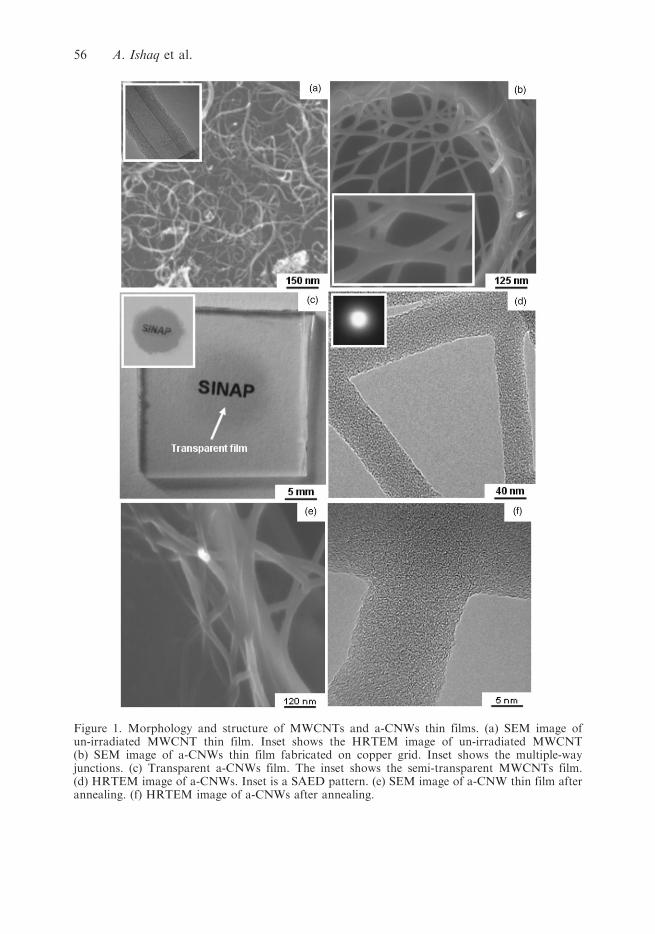
Figure 1. Morphology and structure of MWCNTs and a-CNWs thin films. (a) SEM image ofun-irradiated MWCNT thin film. Inset shows the HRTEM image of un-irradiated MWCNT(b) SEM image of a-CNWs thin film fabricated on copper grid. Inset shows the multiple-wayjunctions. (c) Transparent a-CNWs film. The inset shows the semi-transparent MWCNTs film.(d) HRTEM image of a-CNWs. Inset is a SAED pattern. (e) SEM image of a-CNW thin film afterannealing. (f) HRTEM image of a-CNWs after annealing.
56 A. Ishaq et al.
In addition, ion dose 1� 1017 ions/cm2 for Ar ions is the optimum dose for MWCNTs to
be transformed into a-CNWs [18]. Further, higher doses can destroy a-CNWs and they
could be transformed into carbon films [11]. AFM image of Figure 2(b) shows the surface
morphology of a transparent a-CNW film.
Figure 2. (a) Raman spectra of MWCNTs, a-CNWs and annealed a-CNWs. (b) AFM image ofa-CNWs thin film. (c) AFM height image.
Journal of Experimental Nanoscience 57

Thickness of a-CNW film was measured by AFM using step height method. We took
the average after measurement of every step height, as shown in Figure 2(c). Hence,
average film thickness using AFM is about 200 nm.We have simulated the penetration of ions of energy 70 keV into an amorphous carbon
with density 2.2 g/cm3 using the TRIM code [19], finding that the Ar ions penetrated
approximately 59 nm deep into the carbon target, knocking a large number of carbonatoms from their atomic positions that then contributed to the irradiation damage.
Additionally, the random networks of MWCNTs contain a significant fraction of voids
and higher doses of about 1� 1017 ions/cm2 of Ar ions create high density voids inside the
CNTs, in which the ions and the knocked-out target atoms can move deeper inside the
film. Therefore, both the penetration depth and the lateral spread of defects due to Ar ion
irradiation may be estimated as being five to seven times larger than in the case of a bulk
target. In this study, the Ar ion irradiated film was visually examined (front and back) and
it is observed that most Ar ions at 1� 1017 ions/cm2 dose pass through the MWCNT film
and transform it into a-CNW film. The colour of the whole film transformed fromblackish to grey as shown in Figure 1(c). It means that most of the Ar ions pass through
the film and the new film is highly transparent.The optical properties of a-CNW and MWCNT thin films deposited onto the glass
substrate were investigated using the UV–Vis spectrophotometer. The optical transmission
of the a-CNW and MWCNT films in the wavelength range of 300–900 nm is shown in
Figure 3(a). It is clear that a-CNW film has a higher optical transmission as compared to
MWCNT film and after annealing at 600K, the transmission spectra of a-CNW film is
slightly changed. These transmission spectra reveal that a-CNW film has above 90%
optical transmission. This result suggests that Ar ion beam creates defects which result inlow crystalline structure of the thin film. It is supposed that the decreased crystallinity has
caused the increment of transmission.To study the electrical properties of a-CNW film, the detailed electrical observations
were carried out. I–V response of un-annealed and annealed (at 600K) samples of
Figure 3. Optical and electrical properties of a-CNW thin film. (a) Optical transmission of MWCNTand a-CNW film. (b) The current vs. voltage (I�V) characteristics of the a-CNW thin film beforeand after annealing.
58 A. Ishaq et al.

a-CNWs films at RT on glass substrate were measured by four-point probe method. The
linear I–V plot in Figure 3(b) shows the metallic behaviour of a-CNWs. In addition, it is
observed from Figure 3(b) that the slope of the curve of a-CNW thin film annealed at
600K is higher than a-CNWs thin film at RT. It is concluded that after annealing the
conductivity of film was improved. Conductivity improvement after annealing ascribes
that heat treatment can reduce the defect density in the a-CNW film due to the migration
of carbon atoms.The increment of optical transmission in the whole visible spectral ranges of the
irradiated MWCNT thin film indicates that the creation of the defects in the MWCNTs
might be caused by the ion beam irradiation. It is clearly seen from the TEM images in
Figure 1(d) that the amorphous structures was created by Ar ion bombardment at the dose
of 1� 1017 ions/cm2 and almost all MWCNTs become amorphous. Compared with the
graphite structures of MWCNTs, the light absorption of the amorphous structures of the
irradiated MWCNTs might become small. Broitman et al. [20] reported that the optical
Figure 4. (a) SEM image of a-CNWs. The SEM images of a-CNWs are taken after the focusedelectron beam irradiation at 5min (b), 20min (c) and 50min (d).
Journal of Experimental Nanoscience 59

band of carbon film composed of graphite and amorphous structure was changed due tothe presence of disorder graphite structure. Therefore, one possible reason is that theamorphous carbon structures have some energy gaps and light absorption decreases tosome extent. We will deeply investigate the light transmission and electrical conductivity ofindividual a-CNWs in our future work.
We further, in situ, cut a-CNWs under the focused electron beam. The MWCNTspecimen was firstly irradiated with 25 keV N ion beam at the dose of 1� 1017 ions/cm2 atRT to convert it in to an a-CNW specimen. The SEM image of the irradiated MWCNTs isshown in Figure 4(a). Then, the 15 keV electron beam of the SEM was focused on the areaof a-CNWs, as encircled by the square in Figure 4(a). With increasing time of the electronbeam irradiation, it can be found that the most of the amorphous carbon atoms in thefocus electron beam irradiation area of the a-CNWs have got evaporated and re-depositedand agglomerated around the electron beam irradiation area, as shown in Figure 4(b)–(d).This indicates that the amorphous carbon structure of the a-CNWs almost do not have C–C bonding characteristic. Therefore, a-CNWs are easily cut or destroyed even using 15 keVfocused electron beam of the SEM.
4. Conclusions
In conclusion, we report a simple method to prepare highly transparent a-CNW films onany substrate using the ion beam technique. The change of the electrical conductivity ofa-CNW thin film as a function of temperature show that heat treatment can reduce thedefect density in the a-CNW film due to the migration of carbon atoms. Moreover,a-CNW could be easily cut or destroyed under low energy focus electron beam irradiation.
Acknowledgements
The help of Mr B.N. Ye with the EMIS setup was greatly appreciated. This study was financiallysupported by the Chinese Academy of Sciences Knowledge Innovation Program (grant no.KJCX3.SYW.N10). The corresponding author acknowledges the financial support by thegovernment of Pakistan.
References
[1] E.S. Snow, J.P. Novak, P.M. Campbell, and D. Park, Random networks of carbon nanotubes as an
electronic material, Appl. Phys. Lett. 82 (2003), pp. 2145–2147.
[2] A. Cao, P.M. Ajayan, A. Filin, and P. Persans, Tailoring the optical excitation energies of single-
walled carbon nanotubes, Appl. Phys. Lett. 85 (2004), pp. 1598–1600.
[3] Z. Wu, Z Chen, X. Du, J.M. Logan, J. Sippel, M. Nikolou, K. Kamaras, J.R. Reynolds,
D.B. Tanner, A.F. Hebard, and A.G. Rinzler, Transparent conductive carbon nanotube films,
Science 305 (2004), pp. 1273–1276.
[4] A. Xia, Z. Huizhao, Y. Li, and X. Chengshan, Formation of carbon nanowires by annealing silicon
carbide films deposited by magnetron sputtering, Appl. Surf. Sci. 193 (2002), pp. 87–91.
[5] J.L. Kwo, M. Yokoyama, and I.N. Lin, Characteristics of carbon nanowires synthesized by local
arc-discharging technique, J. Vac. Sci. Technol. B 19 (2001), pp. 1040–1043.
60 A. Ishaq et al.
[6] A. Amma, B. Razavi, S.K.S. Angelo, T.S. Mayer, and T.E. Mallouk, Synthesis, chemicalmodification, and surface assembly of carbon nanowires, Adv. Funct. Mater. 13 (2003),pp. 365–370.
[7] D. Fujita, T. Kumakura, K. Onishi, K. Sagisaka, T. Ohgi, and M. Harada, Sprout-like growth of
carbon nanowires on a carbon-doped Ni(1 1 1) surface, Surf. Sci. 361 (2004), pp. 361–366.[8] A. Kumar, D.K. Avasthi, A. Tripathi, D. Kabiraj, F. Singh, and J.C. Pivin, Synthesis of
confined electrically conducting carbon nanowires by heavy ion irradiation of fullerene thin film, J.
Appl. Phys. 101 (2007), p. 014308.[9] A.M. Zaitsev, A.M. Levine, and S.H. Zaidi, Carbon nanowire-based temperature sensor, Phys.
Status Solidi A 204 (2007), pp. 3574–3579.
[10] A. Kumar, D.K. Avasthi, A. Tripathi, J.D. Carey, D. Fillp, and J.C. Pivin, Formation andcharacterization of carbon nanowires, J. Appl. Phys. 102 (2007), p. 044305.
[11] Z. Ni, Q. Li, D. Zhu, and J. Gong, Fabrication of carbon nanowire networks by Si ion beam
irradiation, Appl. Phys. Lett. 89 (2006), p. 053107.[12] Z. Ni, Q. Li, Y. Long, J. Gong, D. Zhu, and Z. Zhu, Structural change of carbon nanotubes
produced by Si ion beam irradiation, Nucl. Instrum. Methods Phys. Res. B 260 (2007),pp. 542–546.
[13] Z. Wang, L. Yu, W. Zhang, Y. Ding, Y. Li, J. Han, Z. Zhu, H. Xu, G. He, Y. Chen, and G. Hu,Amorphous molecular junctions produced by ion irradiation on carbon nanotubes, Phys. Lett. A324 (2004), pp. 321–325.
[14] Y. Zhu, T. Yi, B. Zheng, and L. Cao, The interaction of C fullerene and carbon nanotube with Arion 60 beam, Appl. Surf. Sci. 137 (1999), pp. 83–90.
[15] H.M. Kim, H.S. Kim, S.K. Park, J. Joo, T.J. Lee, and C.J. Lee, Morphological change of
multiwalled carbon nanotubes through high-energy (MeV) ion irradiation, J. Appl. Phys. 97(2005), p. 026103.
[16] C.H. Jin, J.Y. Wang, Q. Chen, and L.M. Peng, In situ fabrication and graphitization ofamorphous carbon nanowires and their electrical properties, J. Phys. Chem. B 110 (2006),
pp. 5423–5428.[17] A. Kumar, F. Singh, A. Tripathi, J. Pernot, J.C. Pivin, and D.K. Avasthi, Conducting carbon
nanopatterns (nanowire) by energetic ion irradiation, J. Phys. D Appl. Phys. 41 (2008), p. 095304.
[18] A. Ishaq, A.R. Sobia, and L. Yan, Effect of ion irradiation on the properties of carbon nanotubebuckypapers, J. Exp. Nanosci. iFirst (2009), pp. 1–8.
[19] J.P. Biersack and L. Haggmark, A Monte Carlo computer program for the transport of energetic
ions in amorphous targets, Nucl. Instrum. Methods 174 (1980), pp. 257–269.[20] E. Broitman, O.P.A. Lindquist, N. Hellgren, L. Hultman, and B.C. Holloway, Structural,
electrical and optical properties of DLC films deposited by DC magnetron sputtering, J. Vac. Sci.
Technol. A 21 (2003), pp. L23–L27.
Journal of Experimental Nanoscience 61