Review of recent progress of III-nitride nanowire lasers
28
Review of recent progress of III-nitride nanowire lasers Shamsul Arafin Xianhe Liu Zetian Mi Downloaded From: http://nanophotonics.spiedigitallibrary.org/ on 09/24/2013 Terms of Use: http://spiedl.org/terms
Transcript of Review of recent progress of III-nitride nanowire lasers
Review of recent progress of III-nitridenanowire lasers
Shamsul ArafinXianhe LiuZetian Mi
Downloaded From: http://nanophotonics.spiedigitallibrary.org/ on 09/24/2013 Terms of Use: http://spiedl.org/terms
Review of recent progress of III-nitride nanowire lasers
Shamsul Arafin, Xianhe Liu, and Zetian MiMcGill University, Department of Electrical and Computer Engineering,
3480 University Street, Montreal, Quebec H3A 0E9, [email protected]
Abstract. One-dimensional compound semiconductor nanolasers, especially nanowire (NW)-based nanolasers utilizing III-nitride (AlGaInN) materials system, are an emerging andpromising area of research. Significant achievements have been made in developing III-nitrideNW lasers with emission wavelengths from the deep ultraviolet (UV) to the near-infrared spec-tral range. The types of lasers under investigation include Fabry-Pérot, photonic crystal, plas-monic, ring resonator, microstadium, random, polariton, and two-dimensional distributedfeedback lasers. The lasing thresholds vary by several orders of magnitude, which are a directconsequence of differing NW dimensions, quality of the NWs, characteristics of NW cavities,and coupling with the substrate. For electrically injected, such as ultralow-threshold and con-tinuous-wave III-nitride NW lasers that can operate at room temperature, the following obstaclesremain: carrier loss mechanisms including defect-related nonradiative surface recombination,electron overflow, and poor hole transport; low radiative recombination efficiency and highsurface recombination; poor thermal management; and highly resistive ohmic contacts onthe p-layer. These obstacles must be overcome to fully realize the potential of these lasers.© 2013 Society of Photo-Optical Instrumentation Engineers (SPIE) [DOI: 10.1117/1.JNP.7.074599]
Keywords: III-nitride nanowires; nanowire heterostructures; nanolasers; GaN; photolumines-cence; Fabry-Pérot; plasmonics; random lasing.
Paper 13045V received Jun. 2, 2013; revised manuscript received Aug. 7, 2013; accepted forpublication Aug. 9, 2013; published online Sep. 20, 2013.
1 Introduction
Semiconductor one-dimensional (1-D) nanostructures have emerged as a key component for awide range of electronic and optoelectronic applications since their first demonstration in1964.1,2 Currently, a great deal of attention has been paid to semiconductor nanowires(NWs) due to their unique electronic and optical properties arising from the anisotropic geom-etry, the large surface-to-volume ratios, and the unique carrier and photon confinement in twodimensions. One of the most attractive advantages of NWs is that they can be grown either withor without an epitaxial connection to a substrate, which relieves us from lattice and thermalexpansion coefficients mismatch problems in these structures.3–5 This results in, in principle,materials that are free from strain, dislocations, and other structural defects. Therefore, NWshold great promise in a number of applications including electronics,6,7 photovoltaics,8 solid-state lighting,9 and biosensing.10
Furthermore, in order to increase the applicability of NWs as light sources, recent investi-gations have been focused on making semiconductor lasers utilizing NWs compatible with verylarge scale integration (VLSI) circuits. In other words, implementing such digital photonic VLSIsystems requires lasers at nanoscale dimensions. Apart from that, lasers with a reduced dimen-sionality will also allow for developing efficient, low-threshold, and compact light sources formany novel applications in high-speed communications, information processing, and opticalinterconnects. Thus, there is an urgent need to reduce the size of semiconductor lasers. As aconsequence, size reduction of lasers has become one of the most interesting and challengingareas in modern optoelectronics. This is not only for using them as light sources in such
0091-3286/2013/$25.00 © 2013 SPIE
REVIEW
Journal of Nanophotonics 074599-1 Vol. 7, 2013
Downloaded From: http://nanophotonics.spiedigitallibrary.org/ on 09/24/2013 Terms of Use: http://spiedl.org/terms
applications, but also for understanding the basic laser concepts and fundamental light-matterinteractions at the nanoscale.
The smallest application-suited lasers available commercially today are vertical-cavity sur-face-emitting lasers (VCSELs).11 Compared with VCSELs, NW lasers can exhibit much smallerdimensions with diameters of ∼100 nm or less, and therefore, they promise much lower powerconsumption and higher integration density. It should be noticed that in spite of their small cylin-drical dimensions, their lengths can vary from a few hundred nanometers to several or tens ofmicrometers. Also, NWs as gain regions are expected to exhibit superior performance due totheir strong carrier confinement and enhanced electronic density of states. In addition, nearlydefect-free NWs can be grown directly on silicon (Si) substrates;12–17 thereby allowing for themonolithic integration of efficient light emitters with other electronic and photonic componentson a Si platform for the emerging chip-level optical communications.
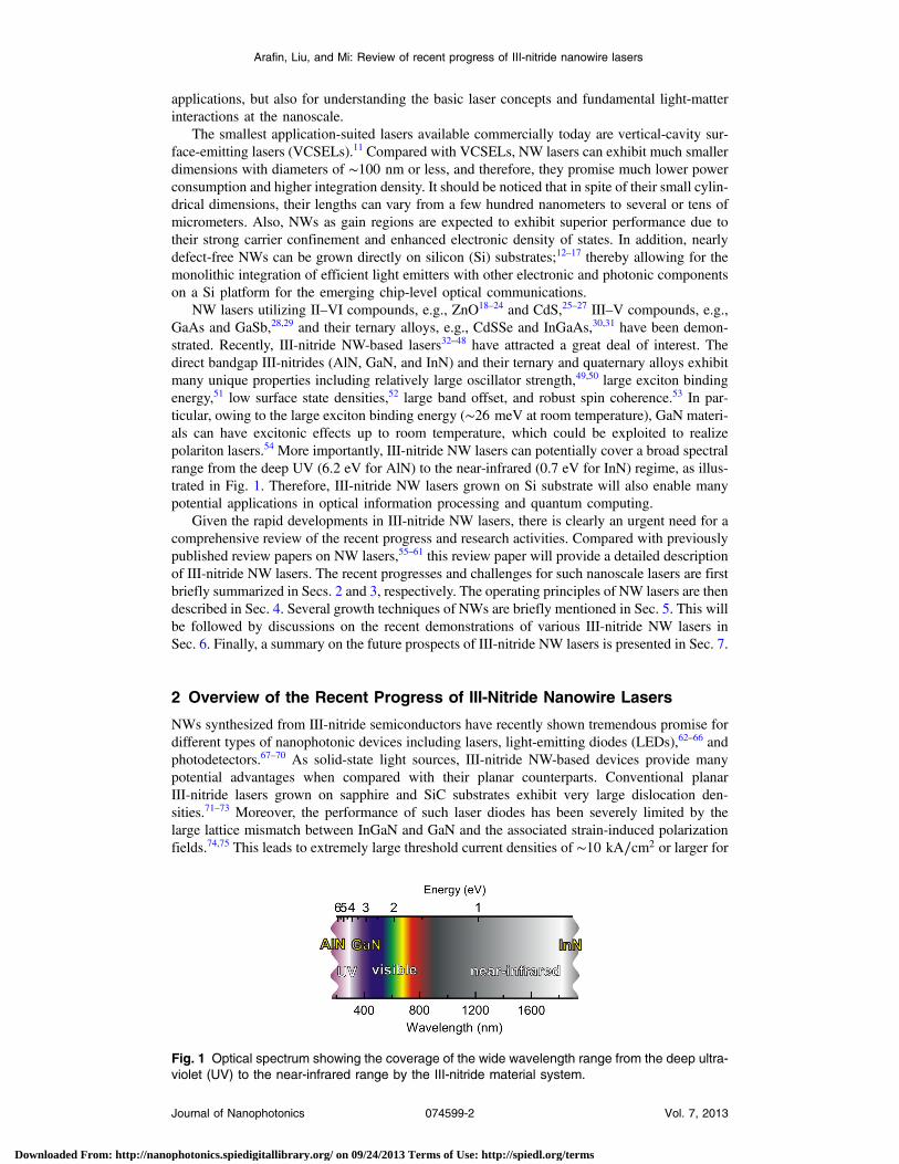
NW lasers utilizing II–VI compounds, e.g., ZnO18–24 and CdS,25–27 III–V compounds, e.g.,GaAs and GaSb,28,29 and their ternary alloys, e.g., CdSSe and InGaAs,30,31 have been demon-strated. Recently, III-nitride NW-based lasers32–48 have attracted a great deal of interest. Thedirect bandgap III-nitrides (AlN, GaN, and InN) and their ternary and quaternary alloys exhibitmany unique properties including relatively large oscillator strength,49,50 large exciton bindingenergy,51 low surface state densities,52 large band offset, and robust spin coherence.53 In par-ticular, owing to the large exciton binding energy (∼26 meV at room temperature), GaN materi-als can have excitonic effects up to room temperature, which could be exploited to realizepolariton lasers.54 More importantly, III-nitride NW lasers can potentially cover a broad spectralrange from the deep UV (6.2 eV for AlN) to the near-infrared (0.7 eV for InN) regime, as illus-trated in Fig. 1. Therefore, III-nitride NW lasers grown on Si substrate will also enable manypotential applications in optical information processing and quantum computing.
Given the rapid developments in III-nitride NW lasers, there is clearly an urgent need for acomprehensive review of the recent progress and research activities. Compared with previouslypublished review papers on NW lasers,55–61 this review paper will provide a detailed descriptionof III-nitride NW lasers. The recent progresses and challenges for such nanoscale lasers are firstbriefly summarized in Secs. 2 and 3, respectively. The operating principles of NW lasers are thendescribed in Sec. 4. Several growth techniques of NWs are briefly mentioned in Sec. 5. This willbe followed by discussions on the recent demonstrations of various III-nitride NW lasers inSec. 6. Finally, a summary on the future prospects of III-nitride NW lasers is presented in Sec. 7.
2 Overview of the Recent Progress of III-Nitride Nanowire Lasers
NWs synthesized from III-nitride semiconductors have recently shown tremendous promise fordifferent types of nanophotonic devices including lasers, light-emitting diodes (LEDs),62–66 andphotodetectors.67–70 As solid-state light sources, III-nitride NW-based devices provide manypotential advantages when compared with their planar counterparts. Conventional planarIII-nitride lasers grown on sapphire and SiC substrates exhibit very large dislocation den-sities.71–73 Moreover, the performance of such laser diodes has been severely limited by thelarge lattice mismatch between InGaN and GaN and the associated strain-induced polarizationfields.74,75 This leads to extremely large threshold current densities of ∼10 kA∕cm2 or larger for
Fig. 1 Optical spectrum showing the coverage of the wide wavelength range from the deep ultra-violet (UV) to the near-infrared range by the III-nitride material system.
Arafin, Liu, and Mi: Review of recent progress of III-nitride nanowire lasers
Journal of Nanophotonics 074599-2 Vol. 7, 2013
Downloaded From: http://nanophotonics.spiedigitallibrary.org/ on 09/24/2013 Terms of Use: http://spiedl.org/terms
devices emitting in the wavelength (λ) range beyond ∼500 nm.76–80 In contrast, NW-based devi-ces can exhibit drastically reduced dislocation densities and polarization fields and can provide agreater degree of flexibility for sophisticated device engineering.66,81 Therefore, III-nitride NWlasers are expected to exhibit much reduced threshold current densities and lower power con-sumption. Moreover, such nanoscale lasers with a reduced cavity volume can potentially operateat much higher modulation speed.82 In addition to these significant advantages, NW-based laserscan promise droop-free operation.83
With the use of III-nitride NW structures, nanolasers with emission wavelengths rangingfrom the deep UV to the near-infrared have already been demonstrated. Many differenttypes of micro- and nanocavities have been studied which include Fabry-Pérot32–34,36,38,46–48
nanoplasmonics,43,45 photonic-crystals,40 microstadium,37 and ring cavities.35 GaN-based NWpolariton laser also has been demonstrated.42 Stimulated emission has been reported utilizingtwo-dimensional (2-D) distributed feedback (DFB) concept in an InGaN nanocolumnarray.39,41 In addition, random lasing action from GaN quasicrystal nanorod arrays44 hasbeen observed. Recently, stable single-mode lasing operation from a single46,48 or a pair47 ofcoupled GaN NWs was demonstrated. Table 1 provides a brief summary of III-nitride nanolasersand their corresponding performance parameters demonstrated by different research teams in theworld. These NW laser demonstrations generally involve the use of optical pumping, and theachievement of electrically injected III-nitride NW lasers has remained elusive.
It may be noticed that the lasing thresholds of these lasers vary by several orders of magni-tude, which is a direct consequence of differing NW dimensions, quality of the NWs, character-istics of NW cavities, and coupling with the substrate.
3 Challenges of III-Nitride Nanowire Lasers
For practical applications, it is highly desired to realize electrically injected, ultralow-threshold,and continuous-wave (CW) III-nitride NW lasers that can be operated at room temperature.Some of the major obstacles and difficulties for realizing such devices are briefly describedbelow:
• Due to the highly effective lateral stress relaxation associated with the large surface areas,both the polarization fields and the dislocation densities in NW devices can be significantlyreduced. However, the performance of III-nitride NW devices still suffers from severalcarrier loss mechanisms including defect-related nonradiative surface recombination,84
electron overflow,85,86 and poor hole transport.87 Additionally, it is still under debatewhether Auger recombination plays an important role in the performance of nitride-based devices.88,89
• The performance of NW-based devices may be further degraded by the presence of radial-band bending and surface Fermi-level pinning. Injected charge carriers, i.e., electronsand holes, may be spatially separated, which leads to a reduced radiative recombinationefficiency and an enhanced surface recombination.90,91
• The performance of semiconductor lasers, including the output power and threshold cur-rent, is often limited by thermal effects. For NWs with diameters smaller than the bulkmean free path of hot carriers, theory predicts that the thermal conductivity will bemuch reduced when compared with their bulk counterparts. The thermal conductivityof single GaN NWs with different diameters has been reported.92–94 Unexpectedlysmall values, in the range of 13 to 19 W∕m-K at 300 K, have been observed.92 This clearlyindicates the critical importance of the thermal management of NW lasers.
• To date, the controlled incorporation of n- and p-type dopants in NW structures haveremained challenging, which makes it difficult to achieve electrically injected devices.Recent studies have shown that Si-dopants are preferentially incorporated in the near-surface region of III-nitride NWs, due to the smaller formation energy for substitutionalSi-doping at the surface.95,96 In addition, the achievement of p-type doping in InGaN andInAlN with high In and Al compositions has still been a big concern. As a consequence,it is difficult to make good quality and low-resistive ohmic contacts on the p-layer of thismaterial system.
Arafin, Liu, and Mi: Review of recent progress of III-nitride nanowire lasers
Journal of Nanophotonics 074599-3 Vol. 7, 2013
Downloaded From: http://nanophotonics.spiedigitallibrary.org/ on 09/24/2013 Terms of Use: http://spiedl.org/terms
Table 1 A brief summary of experimental realizations of III-nitride NW lasers listed in chronologi-cal order.
Research team (year)Activelayer Substrate
Max.operatingtemp Threshold λ (nm)
Resonatortype
Univ. of California, Berkeleyand Lawrence BerkeleyNational Laboratory, Berkeley,CA (2002)
GaN c-Sapphire RT 700 nJ∕cm2 370 to380
Fabry-Pérot
Univ. of California, Berkeleyand Lawrence BerkeleyNational Laboratory, Berkeley,CA (2003)
GaN c-Sapphire RT 2 − 3 μJ∕cm2 384 Fabry-Pérot
Harvard Univ.,Cambridge, MA (2005)
GaN c-Sapphire RT 22 kW∕cm2 370 to378
Fabry-Pérot
Univ. of California, Berkeleyand Lawrence BerkeleyNational Laboratory, Berkeley,CA (2006)
GaN c-Sapphire RT 112.5 μJ∕cm2 373 to380
Ring
Academia Sinica, Taipei,National Taiwan Univ., Taipei,National Taiwan Ocean Univ.,Keelung and National TaiwanUniv. of Science and Tech.,Taipei (2007)
InN Silicon 20 K 70 kW∕cm2 1559 to1644
Fabry-Pérot
Korea Univ., Seoul andHarvard Univ., Cambridge, MA(2007)
GaN c-Sapphire RT 1536 kW∕cm2 370 to372
Microstadium
Harvard Univ., Cambridge, MA,Georgia Institute of Tech,Atlanta, GA, Univ. of California,Santa Cruz, CA,Massachusetts Institute ofTech., Cambridge, MA, andKorea Univ. Seoul (2008)
InGaN/GaN
r-Sapphire RT 900 kW∕cm2 383 to478
Fabry-Pérot
Sophia Univ. and JapanScience and TechnologyAgency, Tokyo (2009)
InGaN/GaN
GaN/c-Sapphiretemplate
RT 320 kW∕cm2 470 2-D DFB
University of Michigan, AnnArbor, MI (2011)
GaN Silicon RT 120 kW∕cm2 370 Photoniccrystal
Sophia Univ. and JapanScience and Tech. Agency,Tokyo (2011)
InGaN/GaN
GaN/c-sapphiretemplate
RT 0.42 MW∕cm2 440 to560
2-D DFB
University of Michigan, AnnArbor, MI (2011)
GaN Silicon RT 92.5 nJ∕cm2 366 to372
Polariton
National Tsing-Hua Univ. andNational Chiao-Tung Univ.,Hsinchu (2011)
InGaN/GaN
Silicon 7 K 300 kW∕cm2 533 Plasmonic
National Chiao Tung Univ.,Hsinchu, Academia Sinica,Taipei, Luxtaltek corporation,Miaoli and National Chiao TungUniv., Hsinchu (2012)
GaN GaN/c-sapphiretemplate
RT 5 MW∕cm2 455 to470
Random
National Tsing-Hua Univ.,Hsinchu, Univ. Texas, Austin,TX, National Chiao Tung Univ.,Hsinchu, Chinese Academy ofSciences, Beijing (2012)
InGaN/GaN
Silicon 78 K 3.7 kW∕cm2 510 to522
Plasmonic
Arafin, Liu, and Mi: Review of recent progress of III-nitride nanowire lasers
Journal of Nanophotonics 074599-4 Vol. 7, 2013
Downloaded From: http://nanophotonics.spiedigitallibrary.org/ on 09/24/2013 Terms of Use: http://spiedl.org/terms
• A detailed understanding and precise control of the NW structural, optical and electricaltransport properties are of utmost requirements to design high-performance NW nanolas-ers. The lack of detailed knowledge on these properties represents another limiting factorfor further improving the performance of nitride NW-based lasers.
4 Operating Principle of Nanowire Lasers
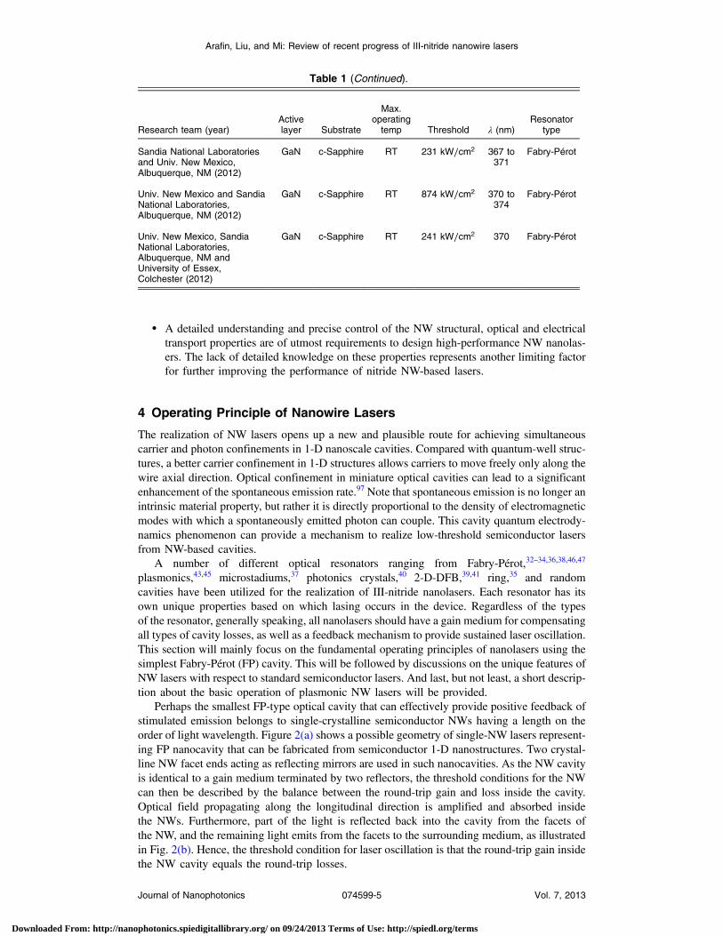
The realization of NW lasers opens up a new and plausible route for achieving simultaneouscarrier and photon confinements in 1-D nanoscale cavities. Compared with quantum-well struc-tures, a better carrier confinement in 1-D structures allows carriers to move freely only along thewire axial direction. Optical confinement in miniature optical cavities can lead to a significantenhancement of the spontaneous emission rate.97 Note that spontaneous emission is no longer anintrinsic material property, but rather it is directly proportional to the density of electromagneticmodes with which a spontaneously emitted photon can couple. This cavity quantum electrody-namics phenomenon can provide a mechanism to realize low-threshold semiconductor lasersfrom NW-based cavities.
A number of different optical resonators ranging from Fabry-Pérot,32–34,36,38,46,47
plasmonics,43,45 microstadiums,37 photonics crystals,40 2-D-DFB,39,41 ring,35 and randomcavities have been utilized for the realization of III-nitride nanolasers. Each resonator has itsown unique properties based on which lasing occurs in the device. Regardless of the typesof the resonator, generally speaking, all nanolasers should have a gain medium for compensatingall types of cavity losses, as well as a feedback mechanism to provide sustained laser oscillation.This section will mainly focus on the fundamental operating principles of nanolasers using thesimplest Fabry-Pérot (FP) cavity. This will be followed by discussions on the unique features ofNW lasers with respect to standard semiconductor lasers. And last, but not least, a short descrip-tion about the basic operation of plasmonic NW lasers will be provided.
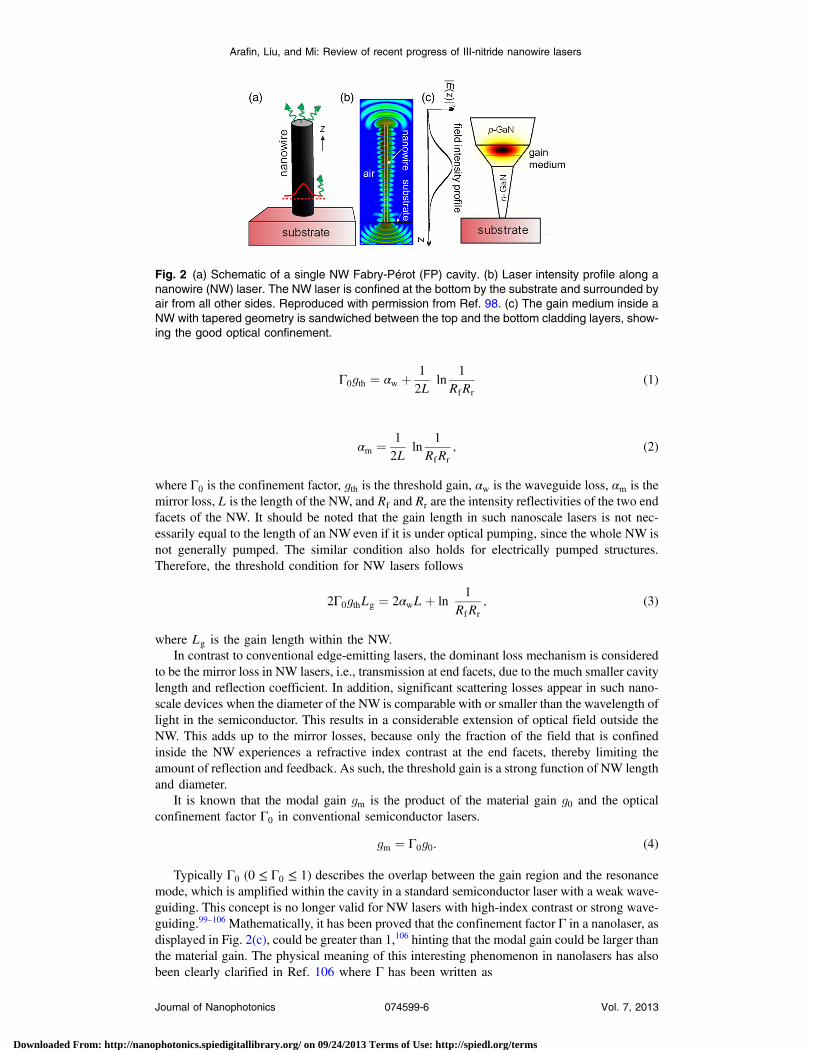
Perhaps the smallest FP-type optical cavity that can effectively provide positive feedback ofstimulated emission belongs to single-crystalline semiconductor NWs having a length on theorder of light wavelength. Figure 2(a) shows a possible geometry of single-NW lasers represent-ing FP nanocavity that can be fabricated from semiconductor 1-D nanostructures. Two crystal-line NW facet ends acting as reflecting mirrors are used in such nanocavities. As the NW cavityis identical to a gain medium terminated by two reflectors, the threshold conditions for the NWcan then be described by the balance between the round-trip gain and loss inside the cavity.Optical field propagating along the longitudinal direction is amplified and absorbed insidethe NWs. Furthermore, part of the light is reflected back into the cavity from the facets ofthe NW, and the remaining light emits from the facets to the surrounding medium, as illustratedin Fig. 2(b). Hence, the threshold condition for laser oscillation is that the round-trip gain insidethe NW cavity equals the round-trip losses.
Table 1 (Continued).
Research team (year)Activelayer Substrate
Max.operatingtemp Threshold λ (nm)
Resonatortype
Sandia National Laboratoriesand Univ. New Mexico,Albuquerque, NM (2012)
GaN c-Sapphire RT 231 kW∕cm2 367 to371
Fabry-Pérot
Univ. New Mexico and SandiaNational Laboratories,Albuquerque, NM (2012)
GaN c-Sapphire RT 874 kW∕cm2 370 to374
Fabry-Pérot
Univ. New Mexico, SandiaNational Laboratories,Albuquerque, NM andUniversity of Essex,Colchester (2012)
GaN c-Sapphire RT 241 kW∕cm2 370 Fabry-Pérot
Arafin, Liu, and Mi: Review of recent progress of III-nitride nanowire lasers
Journal of Nanophotonics 074599-5 Vol. 7, 2013
Downloaded From: http://nanophotonics.spiedigitallibrary.org/ on 09/24/2013 Terms of Use: http://spiedl.org/terms
Γ0gth ¼ αw þ 1
2Lln
1
RfRr
(1)
αm ¼ 1
2Lln
1
RfRr
; (2)
where Γ0 is the confinement factor, gth is the threshold gain, αw is the waveguide loss, αm is themirror loss, L is the length of the NW, and Rf and Rr are the intensity reflectivities of the two endfacets of the NW. It should be noted that the gain length in such nanoscale lasers is not nec-essarily equal to the length of an NWeven if it is under optical pumping, since the whole NW isnot generally pumped. The similar condition also holds for electrically pumped structures.Therefore, the threshold condition for NW lasers follows
2Γ0gthLg ¼ 2αwLþ ln1
RfRr
; (3)
where Lg is the gain length within the NW.In contrast to conventional edge-emitting lasers, the dominant loss mechanism is considered
to be the mirror loss in NW lasers, i.e., transmission at end facets, due to the much smaller cavitylength and reflection coefficient. In addition, significant scattering losses appear in such nano-scale devices when the diameter of the NW is comparable with or smaller than the wavelength oflight in the semiconductor. This results in a considerable extension of optical field outside theNW. This adds up to the mirror losses, because only the fraction of the field that is confinedinside the NW experiences a refractive index contrast at the end facets, thereby limiting theamount of reflection and feedback. As such, the threshold gain is a strong function of NW lengthand diameter.
It is known that the modal gain gm is the product of the material gain g0 and the opticalconfinement factor Γ0 in conventional semiconductor lasers.
gm ¼ Γ0g0: (4)
Typically Γ0 (0 ≤ Γ0 ≤ 1) describes the overlap between the gain region and the resonancemode, which is amplified within the cavity in a standard semiconductor laser with a weak wave-guiding. This concept is no longer valid for NW lasers with high-index contrast or strong wave-guiding.99–106 Mathematically, it has been proved that the confinement factor Γ in a nanolaser, asdisplayed in Fig. 2(c), could be greater than 1,106 hinting that the modal gain could be larger thanthe material gain. The physical meaning of this interesting phenomenon in nanolasers has alsobeen clearly clarified in Ref. 106 where Γ has been written as
Fig. 2 (a) Schematic of a single NW Fabry-Pérot (FP) cavity. (b) Laser intensity profile along ananowire (NW) laser. The NW laser is confined at the bottom by the substrate and surrounded byair from all other sides. Reproduced with permission from Ref. 98. (c) The gain medium inside aNW with tapered geometry is sandwiched between the top and the bottom cladding layers, show-ing the good optical confinement.
Arafin, Liu, and Mi: Review of recent progress of III-nitride nanowire lasers
Journal of Nanophotonics 074599-6 Vol. 7, 2013
Downloaded From: http://nanophotonics.spiedigitallibrary.org/ on 09/24/2013 Terms of Use: http://spiedl.org/terms
Γ ¼ vphvE
Γ0; (5)
where vph is the phase velocity in the gain medium and vE is the energy velocity of the wave-guide. The slower energy velocity of the waveguide mode makes this prefactor more than 1,yielding Γ could be more than 1. Most importantly, the larger modal gain makes it possibleto have a laser with a lower threshold, which becomes very crucial in laser miniaturization.
Another major difference between NWand standard semiconductor lasers is their feedback orcavity mechanism. It is often assumed that a NW laser works as a FP cavity considering similarlocalized reflectors at both ends of the NW. But since the size of NW facets is comparable with orsmaller than the wavelength involved, NW facets behave more like localized scattering centersrather than large planar reflectors considered in a standard FP cavity. Depending on the modes,wavelength, and diameter of the wires, the reflectivity in NWs can be significantly different fromthe results of the Fresnel formula for planar reflectors.107 Since the facet reflectivities determinethe threshold of a laser, a good understanding and an accurate estimation of the facet reflectivitiesare very important and have been discussed in detail in recent publications.102,105,107
Modal characteristics of NWs can be analyzed by cylindrical waveguide theory.108 This isbecause the cylindrical NWs have transverse confinement structure similar to that of the opticalfibers. Hence, the modal characteristics of NWs surrounded by air can be described by a full setof optical modes including transverse electric (TE), transverse magnetic (TM), and their hybridmodes (i.e., HE and EH modes) obtained from a cylindrical dielectric waveguide. Detailedanalysis of modal characteristics in NW lasers can be found elsewhere.58,107,109,110
Like all nanoscale lasers, NW lasers exhibit more complicated far-field emission patternsthan the conventional semiconductor lasers. As the size of lasers gets smaller, larger index con-trast is required to obtain a better waveguiding. This leads to a divergent far-field profile as aresult of fully vectorial (or nonparaxial) propagation.106 Besides, the scattered light output by theNW end facets further complicates the far field. Maslov and Ning107 theoretically analyzed thefar-field emission patterns from individual NWs through a near-field scanning study. But theexperiment was carried out on NWs horizontally lying on a substrate, which is differentfrom the numerical simulation study.32 Further experiments on NWs, either vertically standingor suspended in air, are needed to verify the theoretical prediction. Moreover, a detailed theo-retical understanding of the far-field behavior of a NW on a dielectric or a semiconductor sub-strate is required to compare with the experimental results.107
In most of the experimental realizations, III-nitride NW lasers are fabricated from homo-geneous semiconductors, such as GaN, utilizing the simplest FP cavity. However, poor reflec-tivity with less than 25% at both top and bottom facets requires the NW to be as long as severaltens of micrometers, in order to achieve lasing action. Due to the requirement of such unreal-istically long NWs, achieving high-performance single NW lasers is fundamentally a techno-logical challenge. Furthermore, on the way toward achieving wavelength tunable nanolasers, onecould think of using InGaN embedded in NWs which could serve as a composition-variable gainmedium. But the gain from the nanostructures with small volume is too low to overcome thecavity and high-mirror losses. Most importantly, significant scattering loss prevents smallerdiameter NWs from lasing.
While recently reported dielectric optical microcavities, including microdisks, microposts,photonic crystals and metal claddings are approaching small-scale cavities, their physicalsizes are larger than the emission wavelength for the effective confinement of photons. In con-trast, plasmonics open up a new route for the strong confinement of light to a fraction of theirfreespace wavelength. Their unique dispersion relations enable propagation of light at shortwavelengths along the metal-dielectric interfaces, making it possible to realize optical cavitieswith subwavelength mode volume and high-quality factor (Q). This results in an enhanced light-matter interaction and an increased spontaneous emission and strong coupling in quantumelectrodynamics in such nanocavities. Furthermore, a giant modal gain can be achieved insuch plasmonic nanocavity due to an even higher confinement factor defined in Eq. (5) for com-pletely FP-based nanocavity.95 Importantly, the existence of this giant modal gain near the sur-face plasmon polariton (SPP) resonance will play an important role in achieving the smallestnanolasers; also due to the cost effectiveness and simplicity, the nanoplasmonic concept seems to
Arafin, Liu, and Mi: Review of recent progress of III-nitride nanowire lasers
Journal of Nanophotonics 074599-7 Vol. 7, 2013
Downloaded From: http://nanophotonics.spiedigitallibrary.org/ on 09/24/2013 Terms of Use: http://spiedl.org/terms
be one of the most suitable approaches toward the realization of single NW lasers. For an opti-mized design of NW plasmonic laser, it is important to understand the basic operation of plas-monic FP nanolasers, which are presented elsewhere.111–113
5 Growth of III-Nitride NWs
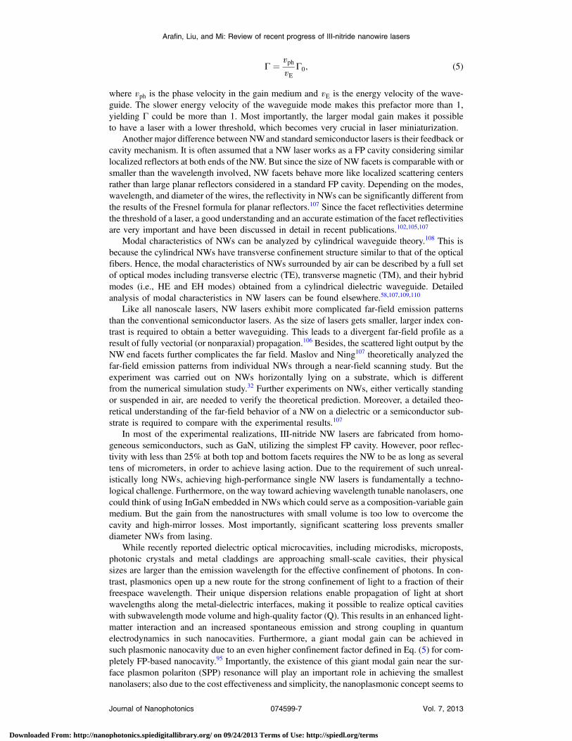
Various methods have been developed for the growth and the synthesis of III-nitride NWs. Themost commonly used methods for GaN NWs are chemical vapor deposition (CVD) and molecu-lar beam epitaxy (MBE). NWs grown using these methods could have hexagonal, triangular, orrectangular cross-sectional areas, as displayed in Fig. 3. GaN NWs grown by metalorganicchemical vapor deposition (MOCVD) can exhibit either hexagonal or triangular cross-sec-tions.114,115 High-quality InGaN NWs can also be grown by many methods includingCVD,81,116 MBE,12,81,116–118 and hydride vapor phase epitaxy.119,120 Recently, significant effortshave already been devoted to the development of various InGaN NW heterostructures includingcore-shell,81,121 well/disk-in-a-wire,122,123 and dot-in-a-wire12,66 based nanostructures, whereinlarge bandgap GaN or AlGaN layers are often employed as the barrier or the shell structuresto provide effective radial and/or axial carrier confinement. Currently, various InN nanostruc-tures, such as nanocrystals,124 nanocolumns,125 nanorods,126 NWs,96 nanotubes, nanotips,127 andnanobelts,36 have been extensively reported.
6 Demonstration of III-Nitride Nanowire Lasers
In the following sections, we will discuss the representative examples of experimentallydemonstrated III-nitride NW lasers. The structural descriptions of each NW laser will alsobe briefly provided. These exemplary devices are classified based on their cavity configurationsand feedback mechanisms employed.
6.1 Fabry-Pérot Lasers
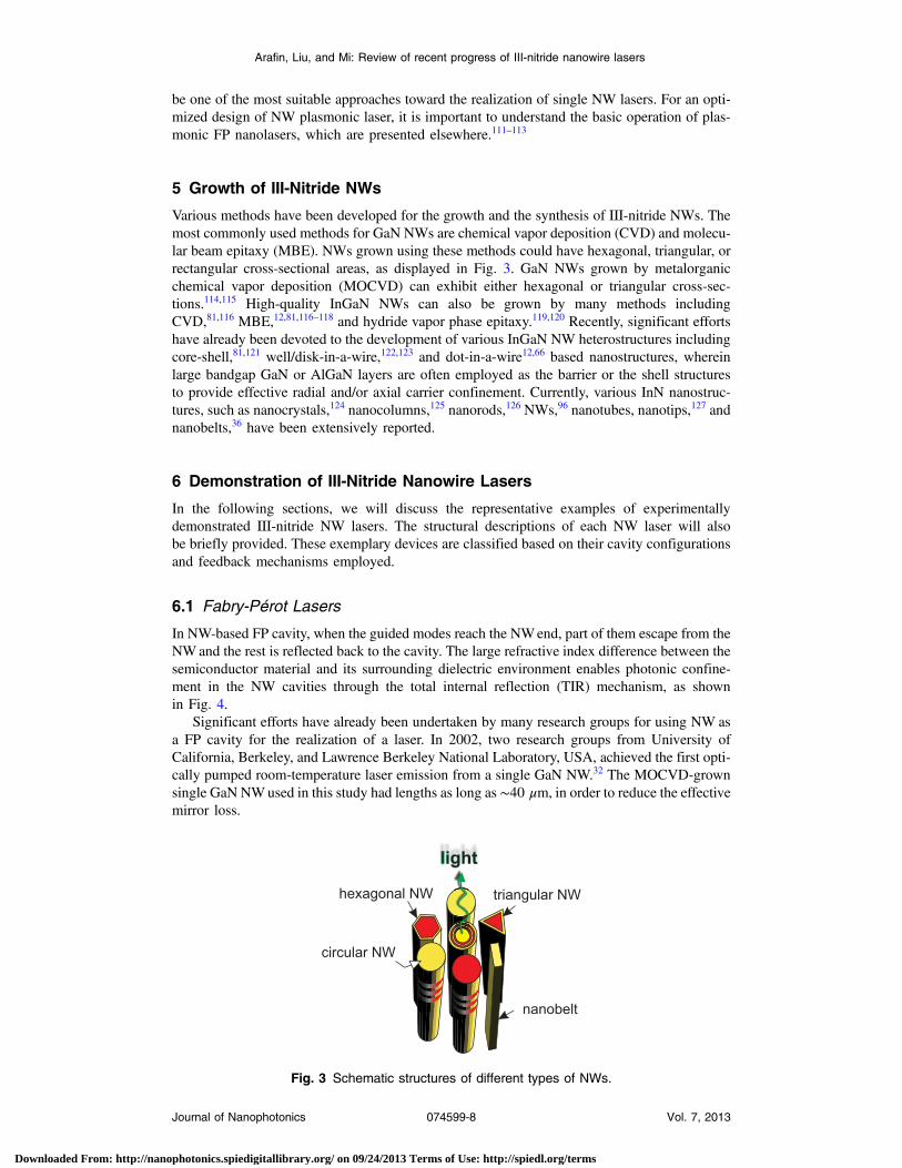
In NW-based FP cavity, when the guided modes reach the NWend, part of them escape from theNWand the rest is reflected back to the cavity. The large refractive index difference between thesemiconductor material and its surrounding dielectric environment enables photonic confine-ment in the NW cavities through the total internal reflection (TIR) mechanism, as shownin Fig. 4.
Significant efforts have already been undertaken by many research groups for using NW asa FP cavity for the realization of a laser. In 2002, two research groups from University ofCalifornia, Berkeley, and Lawrence Berkeley National Laboratory, USA, achieved the first opti-cally pumped room-temperature laser emission from a single GaN NW.32 The MOCVD-grownsingle GaN NWused in this study had lengths as long as ∼40 μm, in order to reduce the effectivemirror loss.
hexagonal NW triangular NW
circular NW
nanobelt
llight
Fig. 3 Schematic structures of different types of NWs.
Arafin, Liu, and Mi: Review of recent progress of III-nitride nanowire lasers
Journal of Nanophotonics 074599-8 Vol. 7, 2013
Downloaded From: http://nanophotonics.spiedigitallibrary.org/ on 09/24/2013 Terms of Use: http://spiedl.org/terms
One year later, UV lasing from optically pumped GaN∕AlxGa1−xN core-sheath quantumwires was demonstrated by the same research group.23 Vapor-liquid-solid (VLS) epitaxial proc-ess was employed to grow cylindrical GaN cores with diameters as small as 5 nm cladded by a50- to 100-nm layer of Al0.75Ga0.25N. Normally, GaN NWs with diameters less than ∼100 nm
are too leaky to sustain laser cavity modes. Surrounding slender GaN wires with a material oflarger bandgap and smaller refractive index creates a structure with simultaneous exciton andphoton confinements. According to the authors, the core provides a gain medium, while thesheath acts as a FP cavity under optical pumping. Significantly, blueshifted PL, which is a sig-nature of the quantum confinement effect, was observed from such unique nanostructures. Butthe lasing threshold was roughly 10 times higher than those of larger, unclad GaN NW lasers.32
In 2005, Gradečak et al. from Harvard University (USA) reported new optical studies of GaNNWs, which exhibited stimulated emission with lower lasing thresholds34 when compared withthe results achieved in 2002.32 Such ultraviolet-blue emitting devices also operated at room tem-perature. The authors believed that NWs with improved structural characteristics led to excellentfree-standing FP cavities, which, together with reduced deep-level defect-related emission byn-type doping, could further reduce the threshold pump power.
Again 1 year later, infrared lasing from single-crystalline InN NWs with belt geometry wasdemonstrated by research teams from Taiwan.36 Nanobelts employed into this study were grownby MOCVD and had well-faceted morphologies with atomically smooth surfaces. Such nanobeltshad widths ranging from 40 to 250 nm, thicknesses from 10 to 35 nm, and length of ∼60 μm.Lasing action from such unique nanostructures was observed at 20 K under CWoptical pumping.
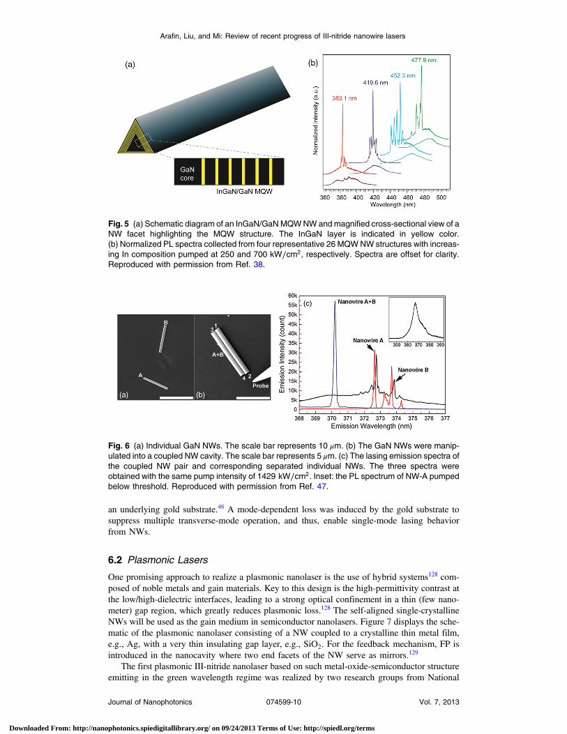
A new type of tunable nanolaser was described by Qian et al. from Harvard University (USA)and Georgia Institute of Technology (USA) in 2008,38 which involved the use of multiquantum-well (MQW) core/shell NW heterostructures. Lasing over a broad range of wavelengths at roomtemperature was reported here. In particular, the structure consists of a GaN NW core that acts asthe optical cavity surrounded by InGaN/GaN MQW shells [see Fig. 5(a)] that serve as a com-position-tunable gain medium. Such NW heterostructure contains 3 to 26 QWs. In this study,dimensions of NWs were 200 to 400 nm in diameter and 20 to 60 μm in length. By varying theindium content, the emission wavelength can be tuned between 365 and 494 nm, as shown inFig. 5(b).
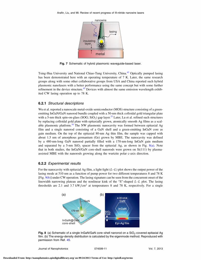
Recently, research groups from University of New Mexico, USA, and Sandia NationalLaboratory, USA, developed the first single-mode NW laser with a side-mode suppressionratio (SMSR) of more than 18 dB by using GaN NWs.46 Devices were optically pumpedand lased at 370 nm with a threshold of 231 kW∕cm2. Then, the same research groups achieveda stable single-mode (SMSR > 15 dB) operation in coupled GaN NW cavities utilizing Verniereffect as a mode-selecting mechanism.47 Such a coupled cavity was realized in this study byplacing two NWs side-by-side in contact to form a NW pair, as displayed in Figs. 6(a) and6(b). According to the authors, Vernier effect plays a major role in suppressing the multipletransverse-mode oscillation as well as multiple longitude-mode oscillation of the GaN NW,where its diameter is much larger than the wavelength. Devices were optically pumped andlased at 370 nm [Fig. 6(c)] with a threshold of 874 kW∕cm2.
Very recently, the same research groups together with researchers at the University of Essex,UK, have demonstrated a mechanism for lasing-mode selection by coupling a GaN NW laser to
Fig. 4 (a) Schematic of a circular NW-based FP cavity. (b) Schematic of light propagation in a NWlongitudinal cavity.
Arafin, Liu, and Mi: Review of recent progress of III-nitride nanowire lasers
Journal of Nanophotonics 074599-9 Vol. 7, 2013
Downloaded From: http://nanophotonics.spiedigitallibrary.org/ on 09/24/2013 Terms of Use: http://spiedl.org/terms
an underlying gold substrate.48 A mode-dependent loss was induced by the gold substrate tosuppress multiple transverse-mode operation, and thus, enable single-mode lasing behaviorfrom NWs.
6.2 Plasmonic Lasers
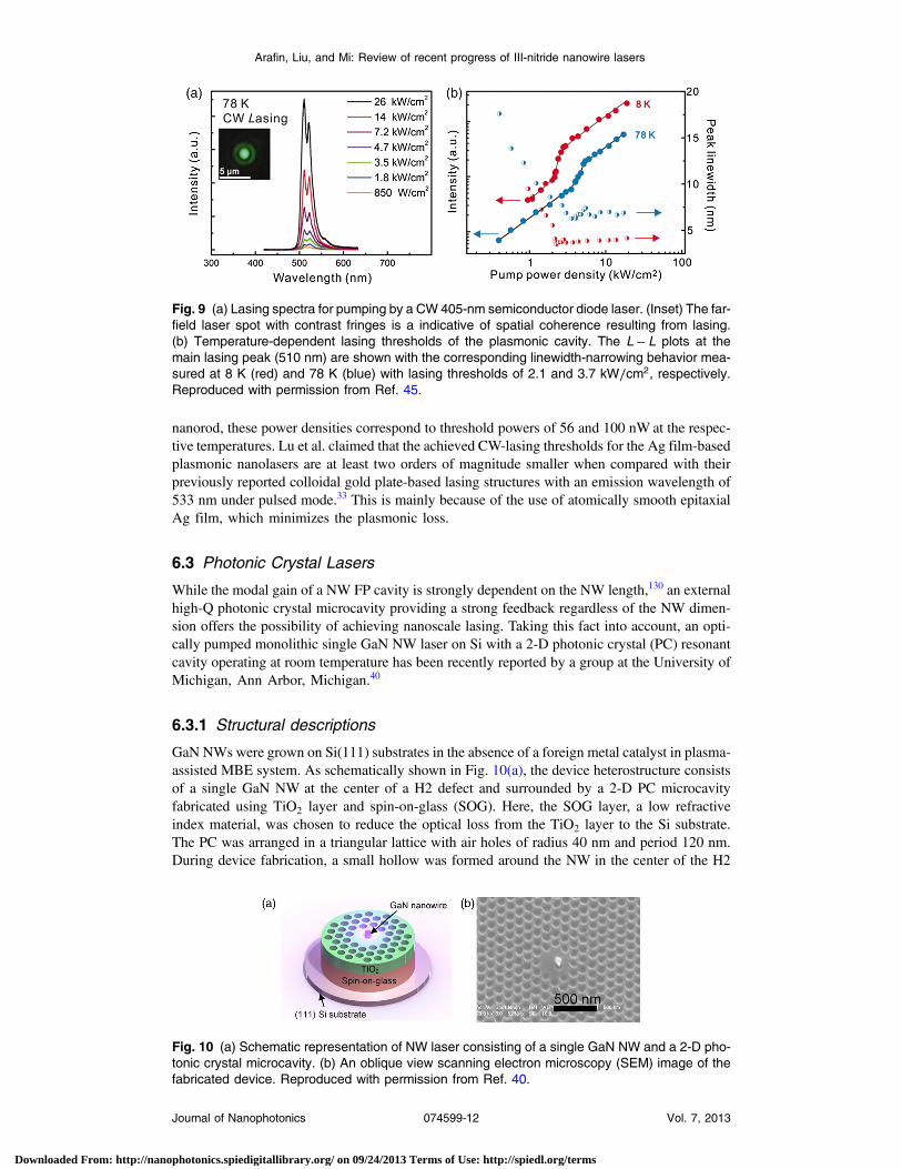
One promising approach to realize a plasmonic nanolaser is the use of hybrid systems128 com-posed of noble metals and gain materials. Key to this design is the high-permittivity contrast atthe low/high-dielectric interfaces, leading to a strong optical confinement in a thin (few nano-meter) gap region, which greatly reduces plasmonic loss.128 The self-aligned single-crystallineNWs will be used as the gain medium in semiconductor nanolasers. Figure 7 displays the sche-matic of the plasmonic nanolaser consisting of a NW coupled to a crystalline thin metal film,e.g., Ag, with a very thin insulating gap layer, e.g., SiO2. For the feedback mechanism, FP isintroduced in the nanocavity where two end facets of the NW serve as mirrors.129
The first plasmonic III-nitride nanolaser based on such metal-oxide-semiconductor structureemitting in the green wavelength regime was realized by two research groups from National
Fig. 5 (a) Schematic diagram of an InGaN/GaNMQWNWandmagnified cross-sectional view of aNW facet highlighting the MQW structure. The InGaN layer is indicated in yellow color.(b) Normalized PL spectra collected from four representative 26 MQWNW structures with increas-ing In composition pumped at 250 and 700 kW∕cm2, respectively. Spectra are offset for clarity.Reproduced with permission from Ref. 38.
Fig. 6 (a) Individual GaN NWs. The scale bar represents 10 μm. (b) The GaN NWs were manip-ulated into a coupled NW cavity. The scale bar represents 5 μm. (c) The lasing emission spectra ofthe coupled NW pair and corresponding separated individual NWs. The three spectra wereobtained with the same pump intensity of 1429 kW∕cm2. Inset: the PL spectrum of NW-A pumpedbelow threshold. Reproduced with permission from Ref. 47.
Arafin, Liu, and Mi: Review of recent progress of III-nitride nanowire lasers
Journal of Nanophotonics 074599-10 Vol. 7, 2013
Downloaded From: http://nanophotonics.spiedigitallibrary.org/ on 09/24/2013 Terms of Use: http://spiedl.org/terms
Tsing-Hua University and National Chiao-Tung University, China.43 Optically pumped lasinghas been demonstrated here with an operating temperature of 7 K. Later, the same researchgroups along with some other collaborative groups from USA and China reported such hybridplasmonic nanolasers with a better performance using the same concept but with some furtherrefinement in the device structure.45 Devices with almost the same emission wavelength exhib-ited CW lasing operation up to 78 K.
6.2.1 Structural descriptions
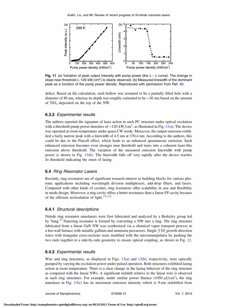
Wu et al. reported a nanoscale metal-oxide semiconductor (MOS) structure consisting of a green-emitting InGaN/GaN nanorod bundle coupled with a 50-nm thick colloidal gold triangular platewith a 5-nm thick spin-on-glass (SOG; SiO2) gap layer.33 Later, Lu et al. refined such structuresby replacing colloidal gold plate with epitaxially grown, atomically smooth Ag films as a scal-able plasmonic platform.34 The NW plasmonic nanocavity was formed between epitaxial Agfilm and a single nanorod consisting of a GaN shell and a green-emitting InGaN core asgain medium. On the top of the epitaxial 80-nm Ag thin film, the sample was capped withabout 1.5 nm of amorphous germanium (Ge) grown by MBE. The nanocavity was definedby a 480-nm-long GaN nanorod partially filled with a 170-nm-long InGaN gain mediumand separated by a 5-nm SiO2 spacer from the epitaxial Ag, as shown in Fig. 8(a). Notethat in both studies, the InGaN/GaN core-shell nanorods were grown on Si(111) by plasma-assisted MBE with the nanorods growing along the wurtzite polar c-axis direction.
6.2.2 Experimental results
For the nanocavity with epitaxial Ag film, a light-light (L–L) plot shows the output power of thelasing mode at 510 nm as a function of pump power for two different temperatures 8 and 78 K[Fig. 9(b)] under CWoperation. The lasing signature can be seen from the concurrent onset of thelinewidth narrowing plateau and the nonlinear kink of the “S”-shaped L–L plot. The lasingthresholds are 2.1 and 3.7 kW∕cm2 at temperatures 8 and 78 K, respectively. For a single
metal
nanowire
insulating layer
hlasing
Fig. 7 Schematic of hybrid plasmonic waveguide-based laser.
Fig. 8 (a) Schematic of a single InGaN/GaN core–shell nanorod on a SiO2-covered epitaxial Agfilm. (b) The energy-density distribution is calculated by the eigenmode method. Reproduced withpermission from Ref. 45.
Arafin, Liu, and Mi: Review of recent progress of III-nitride nanowire lasers
Journal of Nanophotonics 074599-11 Vol. 7, 2013
Downloaded From: http://nanophotonics.spiedigitallibrary.org/ on 09/24/2013 Terms of Use: http://spiedl.org/terms
nanorod, these power densities correspond to threshold powers of 56 and 100 nW at the respec-tive temperatures. Lu et al. claimed that the achieved CW-lasing thresholds for the Ag film-basedplasmonic nanolasers are at least two orders of magnitude smaller when compared with theirpreviously reported colloidal gold plate-based lasing structures with an emission wavelength of533 nm under pulsed mode.33 This is mainly because of the use of atomically smooth epitaxialAg film, which minimizes the plasmonic loss.
6.3 Photonic Crystal Lasers
While the modal gain of a NW FP cavity is strongly dependent on the NW length,130 an externalhigh-Q photonic crystal microcavity providing a strong feedback regardless of the NW dimen-sion offers the possibility of achieving nanoscale lasing. Taking this fact into account, an opti-cally pumped monolithic single GaN NW laser on Si with a 2-D photonic crystal (PC) resonantcavity operating at room temperature has been recently reported by a group at the University ofMichigan, Ann Arbor, Michigan.40
6.3.1 Structural descriptions
GaN NWs were grown on Si(111) substrates in the absence of a foreign metal catalyst in plasma-assisted MBE system. As schematically shown in Fig. 10(a), the device heterostructure consistsof a single GaN NW at the center of a H2 defect and surrounded by a 2-D PC microcavityfabricated using TiO2 layer and spin-on-glass (SOG). Here, the SOG layer, a low refractiveindex material, was chosen to reduce the optical loss from the TiO2 layer to the Si substrate.The PC was arranged in a triangular lattice with air holes of radius 40 nm and period 120 nm.During device fabrication, a small hollow was formed around the NW in the center of the H2
Fig. 9 (a) Lasing spectra for pumping by a CW 405-nm semiconductor diode laser. (Inset) The far-field laser spot with contrast fringes is a indicative of spatial coherence resulting from lasing.(b) Temperature-dependent lasing thresholds of the plasmonic cavity. The L − L plots at themain lasing peak (510 nm) are shown with the corresponding linewidth-narrowing behavior mea-sured at 8 K (red) and 78 K (blue) with lasing thresholds of 2.1 and 3.7 kW∕cm2, respectively.Reproduced with permission from Ref. 45.
Fig. 10 (a) Schematic representation of NW laser consisting of a single GaN NW and a 2-D pho-tonic crystal microcavity. (b) An oblique view scanning electron microscopy (SEM) image of thefabricated device. Reproduced with permission from Ref. 40.
Arafin, Liu, and Mi: Review of recent progress of III-nitride nanowire lasers
Journal of Nanophotonics 074599-12 Vol. 7, 2013
Downloaded From: http://nanophotonics.spiedigitallibrary.org/ on 09/24/2013 Terms of Use: http://spiedl.org/terms
defect. Based on the calculation, such hollow was assumed to be a partially filled hole with adiameter of 80 nm, whereas its depth was roughly estimated to be ∼30 nm based on the amountof TiO2 deposited on the top of the NW.
6.3.2 Experimental results
The authors reported the signature of laser action in such PC structure under optical excitationwith a threshold pump power densities of ∼120 kW∕cm2, as illustrated in Fig. 11(a). The devicewas operated at room temperature under quasi-CW mode. Moreover, the output emission exhib-ited a fairly narrow peak with a linewidth of 4.5 nm at 370.4 nm. According to the authors, thiscould be due to the Purcell effect, which leads to an enhanced spontaneous emission. Suchenhanced emission becomes even stronger near threshold and turns into a coherent laser-likeemission above threshold. The variation of the measured emission linewidth with pumppower is shown in Fig. 11(b). The linewidth falls off very rapidly after the device reachesits threshold indicating the onset of lasing.
6.4 Ring Resonator Lasers
Recently, ring resonators are of significant research interest as building blocks for various pho-tonic applications including wavelength division multiplexers, add-drop filters, and lasers.Compared with other kinds of cavities, ring resonators offer scalability in size and flexibilityin mode design. Moreover, a ring cavity offers a better resonance than a linear FP cavity becauseof the efficient recirculation of light.131,132
6.4.1 Structural descriptions
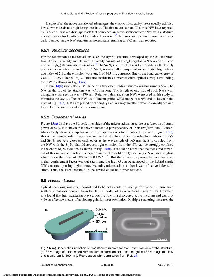
Nitride ring resonator nanolasers were first fabricated and analyzed by a Berkeley group ledby Yang.35 Nanoring resonator is formed by converting a NW into a ring. The ring structurefabricated from a linear GaN NW was synthesized via a chemical vapor transport process ina hot-wall furnace with metallic gallium and ammonia precursors. Single ½ ¯110� growth-directionwires with triangular cross-sections were modified with the micromanipulator by pushing thetwo ends together in a side-by-side geometry to ensure optical coupling, as shown in Fig. 12.
6.4.2 Experimental results
Wire and ring structures, as displayed in Figs. 13(a) and 13(b), respectively, were opticallypumped by varying the excitation power under pulsed operation. Both structures exhibited lasingaction at room temperature. There is a clear change in the lasing behavior of the ring structureas compared with the linear NWs. A significant redshift relative to the linear wire is observedin such ring structures. For example, under similar power fluence (1050 μJ∕cm2), the ringnanolaser in Fig. 13(c) has its maximum emission intensity which is 9-nm redshifted from
Fig. 11 (a) Variation of peak output intensity with pump power (the L − L curve). The change inslope near threshold (∼120 kW∕cm2) is clearly observed. (b) Measured linewidth of the dominantpeak as a function of the pump power density. Reproduced with permission from Ref. 40.
Arafin, Liu, and Mi: Review of recent progress of III-nitride nanowire lasers
Journal of Nanophotonics 074599-13 Vol. 7, 2013
Downloaded From: http://nanophotonics.spiedigitallibrary.org/ on 09/24/2013 Terms of Use: http://spiedl.org/terms
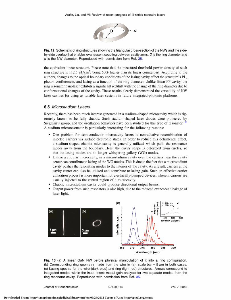
the equivalent linear structure. Please note that the measured threshold power density of suchring structure is 112.5 μJ∕cm2, being 50% higher than its linear counterpart. According to theauthors, changes to the optical boundary conditions of the lasing cavity affect the structure’s PL,photon confinement, and lasing as a function of the ring diameter. Unlike linear FP cavity, thering resonator nanolaser exhibits a significant redshift with the change of the ring diameter due toconformational changes of the cavity. These results clearly demonstrated the versatility of NWlaser cavities for using as tunable laser systems in future integrated-photonic platforms.
6.5 Microstadium Lasers
Recently, there has been much interest generated in a stadium-shaped microcavity which is rig-orously known to be fully chaotic. Such stadium-shaped laser diodes were pioneered bySiegman’s group, and the oscillation behaviors have been studied for this type of resonator.133
A stadium microresonator is particularly interesting for the following reasons:
• One problem for semiconductor microcavity lasers is nonradiative recombination ofinjected carriers via surface electronic states. In order to reduce this detrimental effect,a stadium-shaped chaotic microcavity is generally utilized which pulls the resonancemodes away from the boundary. Here, the cavity shape is deformed from circles, sothat the lasing modes are no longer whispering-gallery (WG) modes.
• Unlike a circular microcavity, in a microstadium cavity even the carriers near the cavitycenter can contribute to lasing of the WGmodes. This is due to the fact that a microstadiumcavity pushes the resonating modes to the interior of the cavity. As a result, carriers at thecavity center can also be utilized and contribute to lasing gain. Such an effective carrierutilization process is more important for electrically-pumped devices, wherein carriers areusually injected to the central region of a microcavity.
• Chaotic microstadium cavity could produce directional output beams.• Output power from such resonators is also high, due to the reduced evanescent leakage of
laser light.
Fig. 12 Schematic of ring structures showing the triangular cross-section of the NWs and the side-by-side overlap that enables evanescent coupling between cavity arms. D is the ring diameter andd is the NW diameter. Reproduced with permission from Ref. 35.
Fig. 13 (a) A linear GaN NW before physical manipulation of it into a ring configuration.(b) Corresponding ring geometry made from the wire in (a); scale bar ¼ 5 μm in both cases.(c) Lasing spectra for the wire (dark blue) and ring (light red) structures. Arrows correspond tointegrated modes within the inset. Inset: modal gain analysis for two separate modes from thering resonator cavity. Reproduced with permission from Ref. 35.
Arafin, Liu, and Mi: Review of recent progress of III-nitride nanowire lasers
Journal of Nanophotonics 074599-14 Vol. 7, 2013
Downloaded From: http://nanophotonics.spiedigitallibrary.org/ on 09/24/2013 Terms of Use: http://spiedl.org/terms
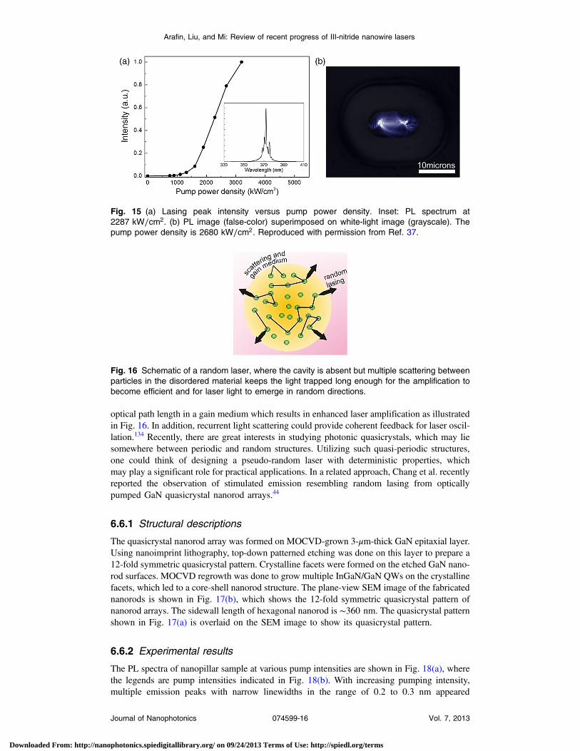
In spite of all the above-mentioned advantages, the chaotic microcavity lasers usually exhibit alow-Q which leads to a high lasing threshold. The first microstadium III-nitride NW laser reportedby Park et al. was a hybrid approach that combined an active semiconductor NW with a stadiummicroresonator for low-threshold stimulated emission.37 Here room-temperature lasing in an opti-cally pumped single NW stadium microresonator emitting at 372 nm was reported.
6.5.1 Structural descriptions
For the realization of microstadium laser, the hybrid structure developed by the collaboratorsfrom Korea University and Harvard University consists of a single-crystal GaN NWand a siliconnitride (Si3N4) stadium microresonator.37 The Si3N4 slab structure was fabricated on a thick SiO2
post with a low refractive index of 1.5. Si3N4 is essentially transparent and exhibits a high refrac-tive index of 2.1 at the emission wavelength of 365 nm, corresponding to the band gap energy ofGaN (∼3.4 eV). Hence, Si3N4 structure establishes a microstadium optical cavity surroundingthe NW, as shown in Fig. 14(a).
Figure 14(b) shows the SEM image of a fabricated stadium microresonator using a NW. TheNW on the top of the stadium was ∼7.5 μm long. The length of one side of such NWs withtriangular cross-section was ∼170 nm. Relatively thin and short NWs were used in this study tominimize the cavity effect of NW itself. The magnified SEM image of a NWend is shown in theinset of Fig. 14(b). NWs are placed on the Si3N4 slab in a way that their two ends are aligned andlocated at the two foci of such microstadium.
6.5.2 Experimental results
Figure 15(a) displays the PL peak intensities of the microstadium structure as a function of pumppower density. It is shown that above a threshold power density of 1536 kW∕cm2, the PL inten-sities clearly show a sharp transition from spontaneous to stimulated emission. Figure 15(b)shows the lasing-mode image measured in the structure. Since the refractive indices of GaNand Si3N4 are very close to each other at the wavelength of 365 nm, light is coupled fromthe NW with the Si3N4 slab. Moreover, light emission from the NW can be strongly confinedin the entire Si3N4 stadium, as shown in Fig. 15(b). It should be noted that the measured thresh-old of this microstadium laser is larger than the threshold of a typical single NW laser on glasswhich is on the order of 100 to 1000 kW∕cm2. But these research groups believe that evenhigher confinement factor without sacrificing the high-Q can be achieved in the hybrid singleNW structure by using higher refractive index microstadium and/or lower refractive index sub-strate. Thus, the laser threshold in the device could be further reduced.
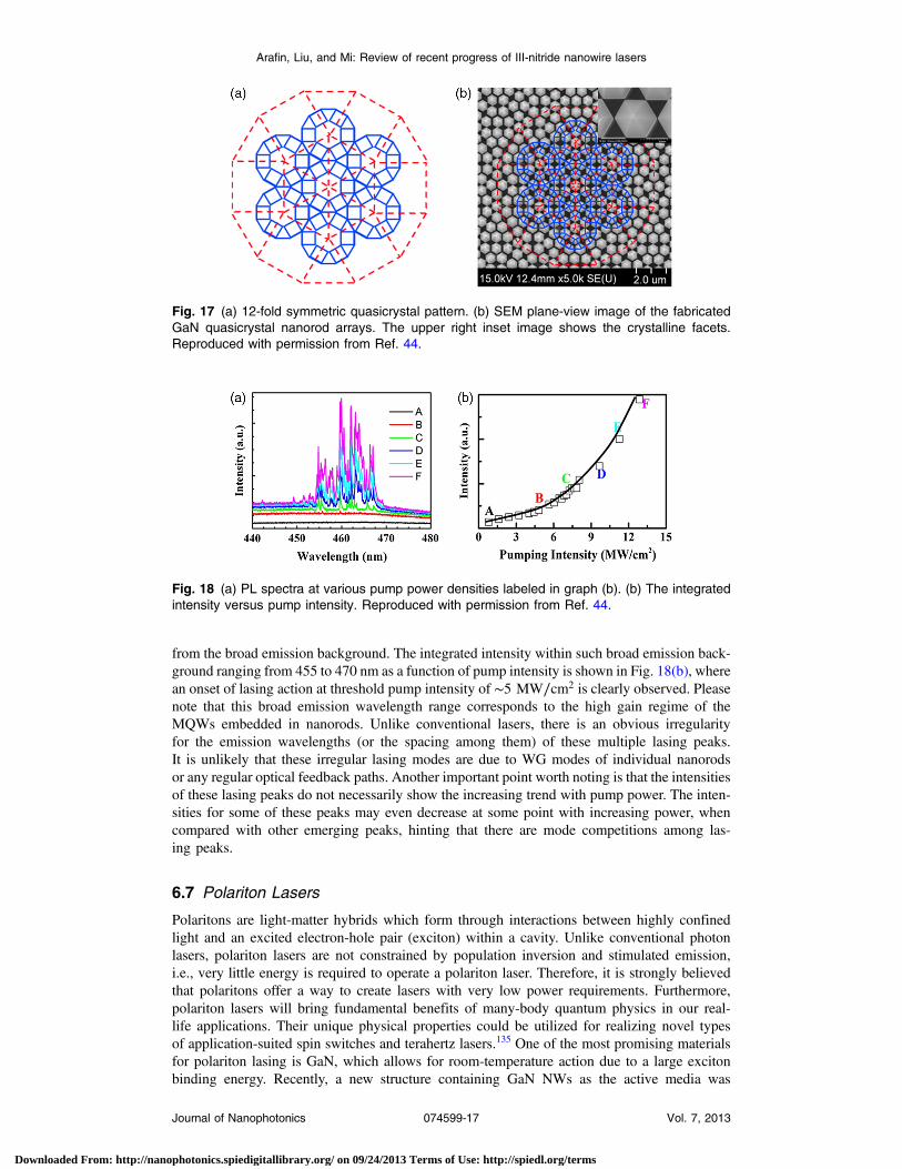
6.6 Random Lasers
Optical scattering was often considered to be detrimental to laser performance, because suchscattering removes photons from the lasing modes of a conventional laser cavity. However,it is found that light scattering plays a positive role in a disordered active medium and can pro-vide an effective means of achieving gain for laser oscillation. Multiple scattering increases the
Fig. 14 (a) Schematic illustration of NW stadium microresonator. Inset: sideview of the structure.(b) SEM image of a fabricated NW stadium microresonator. Inset: magnified SEM image of a NWend (scale bar is 500 nm). Reproduced with permission from Ref. 37.
Arafin, Liu, and Mi: Review of recent progress of III-nitride nanowire lasers
Journal of Nanophotonics 074599-15 Vol. 7, 2013
Downloaded From: http://nanophotonics.spiedigitallibrary.org/ on 09/24/2013 Terms of Use: http://spiedl.org/terms
optical path length in a gain medium which results in enhanced laser amplification as illustratedin Fig. 16. In addition, recurrent light scattering could provide coherent feedback for laser oscil-lation.134 Recently, there are great interests in studying photonic quasicrystals, which may liesomewhere between periodic and random structures. Utilizing such quasi-periodic structures,one could think of designing a pseudo-random laser with deterministic properties, whichmay play a significant role for practical applications. In a related approach, Chang et al. recentlyreported the observation of stimulated emission resembling random lasing from opticallypumped GaN quasicrystal nanorod arrays.44
6.6.1 Structural descriptions
The quasicrystal nanorod array was formed on MOCVD-grown 3-μm-thick GaN epitaxial layer.Using nanoimprint lithography, top-down patterned etching was done on this layer to prepare a12-fold symmetric quasicrystal pattern. Crystalline facets were formed on the etched GaN nano-rod surfaces. MOCVD regrowth was done to grow multiple InGaN/GaN QWs on the crystallinefacets, which led to a core-shell nanorod structure. The plane-view SEM image of the fabricatednanorods is shown in Fig. 17(b), which shows the 12-fold symmetric quasicrystal pattern ofnanorod arrays. The sidewall length of hexagonal nanorod is ∼360 nm. The quasicrystal patternshown in Fig. 17(a) is overlaid on the SEM image to show its quasicrystal pattern.
6.6.2 Experimental results
The PL spectra of nanopillar sample at various pump intensities are shown in Fig. 18(a), wherethe legends are pump intensities indicated in Fig. 18(b). With increasing pumping intensity,multiple emission peaks with narrow linewidths in the range of 0.2 to 0.3 nm appeared
Fig. 15 (a) Lasing peak intensity versus pump power density. Inset: PL spectrum at2287 kW∕cm2. (b) PL image (false-color) superimposed on white-light image (grayscale). Thepump power density is 2680 kW∕cm2. Reproduced with permission from Ref. 37.
Fig. 16 Schematic of a random laser, where the cavity is absent but multiple scattering betweenparticles in the disordered material keeps the light trapped long enough for the amplification tobecome efficient and for laser light to emerge in random directions.
Arafin, Liu, and Mi: Review of recent progress of III-nitride nanowire lasers
Journal of Nanophotonics 074599-16 Vol. 7, 2013
Downloaded From: http://nanophotonics.spiedigitallibrary.org/ on 09/24/2013 Terms of Use: http://spiedl.org/terms
from the broad emission background. The integrated intensity within such broad emission back-ground ranging from 455 to 470 nm as a function of pump intensity is shown in Fig. 18(b), wherean onset of lasing action at threshold pump intensity of ∼5 MW∕cm2 is clearly observed. Pleasenote that this broad emission wavelength range corresponds to the high gain regime of theMQWs embedded in nanorods. Unlike conventional lasers, there is an obvious irregularityfor the emission wavelengths (or the spacing among them) of these multiple lasing peaks.It is unlikely that these irregular lasing modes are due to WG modes of individual nanorodsor any regular optical feedback paths. Another important point worth noting is that the intensitiesof these lasing peaks do not necessarily show the increasing trend with pump power. The inten-sities for some of these peaks may even decrease at some point with increasing power, whencompared with other emerging peaks, hinting that there are mode competitions among las-ing peaks.
6.7 Polariton Lasers
Polaritons are light-matter hybrids which form through interactions between highly confinedlight and an excited electron-hole pair (exciton) within a cavity. Unlike conventional photonlasers, polariton lasers are not constrained by population inversion and stimulated emission,i.e., very little energy is required to operate a polariton laser. Therefore, it is strongly believedthat polaritons offer a way to create lasers with very low power requirements. Furthermore,polariton lasers will bring fundamental benefits of many-body quantum physics in our real-life applications. Their unique physical properties could be utilized for realizing novel typesof application-suited spin switches and terahertz lasers.135 One of the most promising materialsfor polariton lasing is GaN, which allows for room-temperature action due to a large excitonbinding energy. Recently, a new structure containing GaN NWs as the active media was
Fig. 17 (a) 12-fold symmetric quasicrystal pattern. (b) SEM plane-view image of the fabricatedGaN quasicrystal nanorod arrays. The upper right inset image shows the crystalline facets.Reproduced with permission from Ref. 44.
Fig. 18 (a) PL spectra at various pump power densities labeled in graph (b). (b) The integratedintensity versus pump intensity. Reproduced with permission from Ref. 44.
Arafin, Liu, and Mi: Review of recent progress of III-nitride nanowire lasers
Journal of Nanophotonics 074599-17 Vol. 7, 2013
Downloaded From: http://nanophotonics.spiedigitallibrary.org/ on 09/24/2013 Terms of Use: http://spiedl.org/terms
developed by a group at the University of Michigan in Ann Arbor, Michigan, to fabricate polar-iton lasers.42 Such lasers with an emission wavelength of ∼370 nm operate at room temperaturewith an ultralow threshold.
6.7.1 Structural descriptions
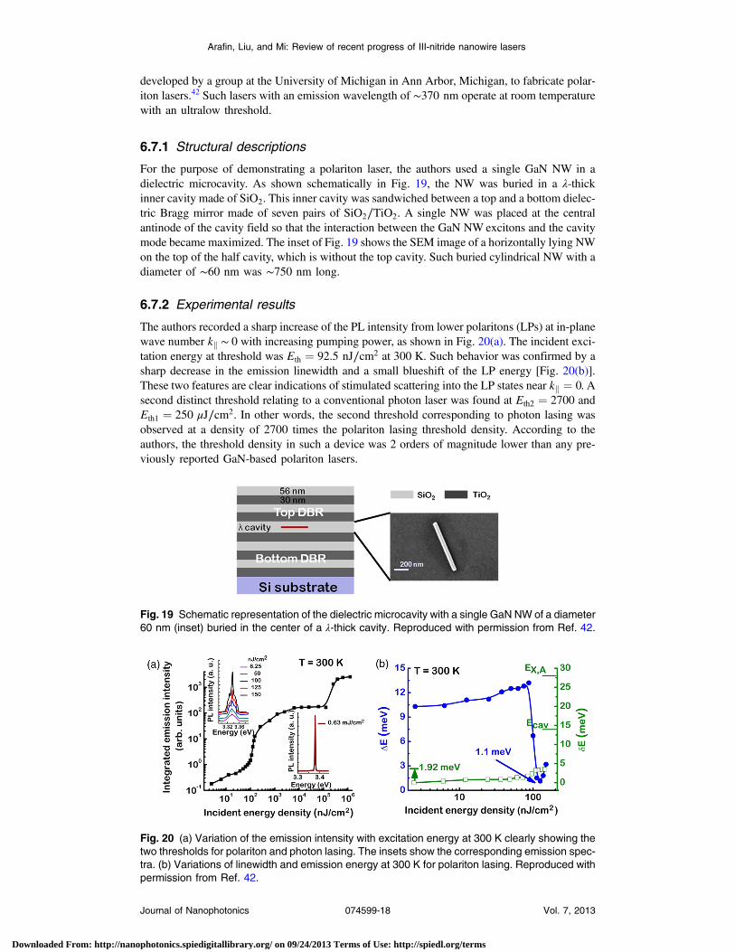
For the purpose of demonstrating a polariton laser, the authors used a single GaN NW in adielectric microcavity. As shown schematically in Fig. 19, the NW was buried in a λ-thickinner cavity made of SiO2. This inner cavity was sandwiched between a top and a bottom dielec-tric Bragg mirror made of seven pairs of SiO2∕TiO2. A single NW was placed at the centralantinode of the cavity field so that the interaction between the GaN NW excitons and the cavitymode became maximized. The inset of Fig. 19 shows the SEM image of a horizontally lying NWon the top of the half cavity, which is without the top cavity. Such buried cylindrical NW with adiameter of ∼60 nm was ∼750 nm long.
6.7.2 Experimental results
The authors recorded a sharp increase of the PL intensity from lower polaritons (LPs) at in-planewave number kk ∼ 0 with increasing pumping power, as shown in Fig. 20(a). The incident exci-tation energy at threshold was Eth ¼ 92.5 nJ∕cm2 at 300 K. Such behavior was confirmed by asharp decrease in the emission linewidth and a small blueshift of the LP energy [Fig. 20(b)].These two features are clear indications of stimulated scattering into the LP states near kk ¼ 0. Asecond distinct threshold relating to a conventional photon laser was found at Eth2 ¼ 2700 andEth1 ¼ 250 μJ∕cm2. In other words, the second threshold corresponding to photon lasing wasobserved at a density of 2700 times the polariton lasing threshold density. According to theauthors, the threshold density in such a device was 2 orders of magnitude lower than any pre-viously reported GaN-based polariton lasers.
Fig. 19 Schematic representation of the dielectric microcavity with a single GaN NW of a diameter60 nm (inset) buried in the center of a λ-thick cavity. Reproduced with permission from Ref. 42.
Fig. 20 (a) Variation of the emission intensity with excitation energy at 300 K clearly showing thetwo thresholds for polariton and photon lasing. The insets show the corresponding emission spec-tra. (b) Variations of linewidth and emission energy at 300 K for polariton lasing. Reproduced withpermission from Ref. 42.
Arafin, Liu, and Mi: Review of recent progress of III-nitride nanowire lasers
Journal of Nanophotonics 074599-18 Vol. 7, 2013
Downloaded From: http://nanophotonics.spiedigitallibrary.org/ on 09/24/2013 Terms of Use: http://spiedl.org/terms
6.8 Two-Dimensional DFB Lasers
Since the first introduction of distributed-feedback (DFB)-based laser by Kogelnik and Shank,136
this concept has undergone rapid developments, in order to obtain lasing action. The fabricationof 2-D-DFB GaInAsP/InP laser diodes was one of the greatest achievements, in which the laserbeam was radiated perpendicularly to the surface.137 The same concept has been applied to thestudy of blue-violet GaN 2-D-DFB laser action, where the periodic air-hole structures inducingthe 2-D light confinement was used.138 Recently, Kouno et al. from Sophia University, Japan,first experimentally demonstrated high-performance 2-D-DFB laser action in the blue wave-length regime using high-density InGaN/GaN nanocolumn array having a dielectric cylinder.39
On the way toward the realization of lasers with green emission wavelength, later Ishizawa et al.reported stimulated emission as 2-D-DFB lasers by employing InGaN-QW nanocolumnarrays.41
6.8.1 Structural descriptions
Kouno et al. used a MOCVD-grown (0001) 3.5-μm thick GaN template, whereas GaNrectangular-lattice nanocolumn arrays with 8-period InGaN/GaN MQWs at the top of thecolumns were grown by RF-MBE.39 Figure 21 displays SEM images of a vertically alignednanocolumn array sample fabricated in this study. Each GaN nanocolumns with a hexagonalcross-section had the side length of 92 nm and the height along the c-axis of approximately850 nm. The GaN nanocolumns were arranged in a rectangular lattice by adjusting a particularhorizontal and vertical lattice constant [see Fig. 21(b)]. Most importantly, the lasing wavelengthof a nanocolumn array is controlled by two parameters, i.e., lattice constant and hexagonal sidelength.
6.8.2 Experimental results
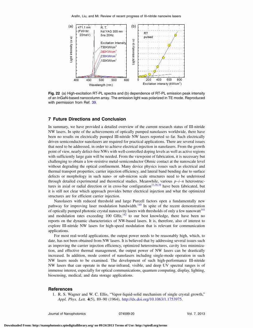
Figure 22(a) displays the RT emission spectra measured by changing the excitation powerintensity, where a sharp and a strong emission peak was observed at 471 nm at a power densityof approximately 320 kW∕cm2. The intensity increased nonlinearly as a function of excitationpower density, as shown in Fig. 22(b). This was the clear signature of the stimulated emission.The 2-D light confinement enhanced the optical gain at this wavelength,139 yielding the stimu-lated emission. Using the similar concept, Ishizawa et al. demonstrated blue to green stimu-lated emission from InGaN-QW nanocolumn arrays, in which the emission wavelength wascontrolled through the structural parameters of the lattice constant and the nanocolumn diam-eter in the wavelength ranges of 440 to 510 and 530 to 560 nm, respectively.41 Note that thelasing threshold for the nanocolumn arrays with a peak emission wavelength of 552 nmappeared at excitation power densities greater than 0.42 MW∕cm2. The authors claimedthat 560 nm was the longest wavelength ever reported for stimulated emission amongInGaN-based QWs.
Fig. 21 SEM images: (a) bird’s-eye and (b) top views of typical regularly arranged GaN nanocol-umns with 8-period InGaN/GaN MQWs. Reproduced with permission from Ref. 39.
Arafin, Liu, and Mi: Review of recent progress of III-nitride nanowire lasers
Journal of Nanophotonics 074599-19 Vol. 7, 2013
Downloaded From: http://nanophotonics.spiedigitallibrary.org/ on 09/24/2013 Terms of Use: http://spiedl.org/terms
7 Future Directions and Conclusion
In summary, we have provided a detailed overview of the current research status of III-nitrideNW lasers. In spite of the achievements of optically pumped nanolasers worldwide, there havebeen no results on electrically pumped III-nitride NW lasers reported so far. Such electricallydriven semiconductor nanolasers are required for practical applications. There are several issuesthat need to be addressed, in order to achieve electrical injection in nanolasers. From the growthpoint of view, nearly defect-free NWs with well-controlled doping levels as well as active regionswith sufficiently large gain will be needed. From the viewpoint of fabrication, it is necessary butchallenging to obtain a low-resistive metal-semiconductor Ohmic contact at the nanoscale levelwithout degrading the optical confinement. Many device physics issues such as electrical andthermal transport properties, carrier injection efficiency, and lateral band bending due to surfacedefects or morphology in such nano- or sub-micron scale structures need to be understoodthrough detailed experimental and theoretical studies. Meanwhile, various p–i–n heterostruc-tures in axial or radial direction or in cross-bar configuration23,28,38 have been fabricated, butit is still not clear which approach provides better electrical injection and what the optimizedstructures are for efficient carrier injection.
Nanolasers with reduced threshold and large Purcell factors open a fundamentally newpathway for improving laser modulation bandwidth.140 In spite of the recent demonstrationof optically pumped photonic crystal nanocavity lasers with thresholds of only a few nanowatt141
and modulation rates exceeding 100 GHz,142 to our best knowledge, there have been noreports on the dynamic characteristics of NW-based lasers. It is, therefore, also of interest toexplore III-nitride NW lasers for high-speed modulation that is relevant for communicationapplications.
For most real-world applications, the output power needs to be reasonably high, which, todate, has not been obtained from NW lasers. It is believed that by addressing several issues suchas improving the carrier injection efficiency, optimized heterostructures, cavity loss minimiza-tion, and effective thermal management, the output power of NW lasers can be drasticallyincreased. In addition, mode control of nanolasers including single-mode operation in suchNW lasers needs to be examined. The development of such high-performance III-nitrideNW lasers that can operate in the near-infrared, visible, and deep UV spectral ranges is ofimmense interest, especially for optical communications, quantum computing, display, lighting,biosensing, medical, and data storage applications.
References1. R. S. Wagner and W. C. Ellis, “Vapor-liquid-solid mechanism of single crystal growth,”
Appl. Phys. Lett. 4(5), 89–90 (1964), http://dx.doi.org/10.1063/1.1753975.
Fig. 22 (a) High-excitation RT-PL spectra and (b) dependence of RT-PL emission peak intensityof an InGaN-based nanocolumn array. The emission light was polarized in TE mode. Reproducedwith permission from Ref. 39.
Arafin, Liu, and Mi: Review of recent progress of III-nitride nanowire lasers
Journal of Nanophotonics 074599-20 Vol. 7, 2013
Downloaded From: http://nanophotonics.spiedigitallibrary.org/ on 09/24/2013 Terms of Use: http://spiedl.org/terms
2. R. S. Wagner, Whisker Technology, Wiley-Interscience, New York (1970).3. X. Y. Bao et al., “Heteroepitaxial growth of vertical GaAs nanowires on Si(111) substrates
by metal-organic chemical vapor deposition,” Nano Lett. 8(11), 3755–3760 (2008), http://dx.doi.org/10.1021/nl802062y.
4. S. Li and A. Waag, “GaN based nanorods for solid state lighting,” J. Appl. Phys. 111(7),071101 (2012), http://dx.doi.org/10.1063/1.3694674.
5. S. Zhao et al., “Growth of large-scale vertically aligned GaN nanowires and their hetero-structures with high uniformity on SiO(x) by catalyst-free molecular beam epitaxy,”Nanoscale 5(12), 5283–5287 (2013), http://dx.doi.org/10.1039/c3nr00387f.
6. X. Duan et al., “Indium phosphide nanowires as building blocks for nanoscale electronicand optoelectronic devices,” Nature 409(6816), 66–69 (2001), http://dx.doi.org/10.1038/35051047.
7. Y. Cui and C. M. Lieber, “Functional nanoscale electronic devices assembled using siliconnanowire building blocks,” Science 291(5505), 851–853 (2001), http://dx.doi.org/10.1126/science.291.5505.851.
8. Y. Dong et al., “Coaxial group III-nitride nanowire photovoltaics,” Nano Lett. 9(5), 2183–2187 (2009), http://dx.doi.org/10.1021/nl900858v.
9. Y. Huang, X. Duan, and C. M. Lieber, “Nanowires for integrated multicolor nanophoton-ics,” Small 1(1), 142–147 (2005), http://dx.doi.org/10.1002/smll.200400030.
10. A. K. Wanekaya et al., “Nanowire-based electrochemical biosensors,” Electroanalysis18(6), 533–550 (2006), http://dx.doi.org/10.1002/(ISSN)1521-4109.
11. E. Wong et al., “Energy-efficiency of optical network units with vertical-cavity surface-emitting lasers,” Opt. Express 20(14), 14960–14970 (2012), http://dx.doi.org/10.1364/OE.20.014960.
12. Y. L. Chang et al., “High efficiency green, yellow, and amber emission from InGaN/GaNdot-in-a-wire heterostructures on Si(111),” Appl. Phys. Lett. 96(1), 013106 (2010), http://dx.doi.org/10.1063/1.3284660.
13. W. Guo et al., “Catalyst-free InGaN/GaN nanowire light emitting diodes grown on (001)silicon by molecular beam epitaxy,” Nano Lett. 10(9), 3355–3359 (2010), http://dx.doi.org/10.1021/nl101027x.
14. H. P. Nguyen et al., “Controlling electron overflow in phosphor-free InGaN/GaN nanowirewhite light-emitting diodes,” Nano Lett. 12(3), 1317–1323 (2012), http://dx.doi.org/10.1021/nl203860b.
15. J.-H. Kang et al., “Defect-free GaAs/AlGaAs core-shell nanowires on Si substrates,” Cryst.Growth Des. 11(7), 3109–3114 (2011), http://dx.doi.org/10.1021/cg2003657.
16. P. K. Mohseni et al., “GaP/GaAsP/GaP core-multishell nanowire heterostructures on (111)silicon,” Nanotechnology 18(44), 445304 (2007), http://dx.doi.org/10.1088/0957-4484/18/44/445304.
17. G. Koblmuller et al., “Self-induced growth of vertical free-standing InAs nanowires on Si(111) by molecular beam epitaxy,” Nanotechnology 21(36), 365602 (2010), http://dx.doi.org/10.1088/0957-4484/21/36/365602.
18. M. Law et al., “Nanoribbon waveguides for subwavelength photonics integration,” Science305(5688), 1269–1273 (2004), http://dx.doi.org/10.1126/science.1100999.
19. L. K. van Vugt, S. Rühle, and D. Vanmaekelbergh, “Phase-correlated nondirectional laseremission from the end facets of a ZnO nanowire,” Nano Lett. 6(12), 2707–2711 (2006),http://dx.doi.org/10.1021/nl0616227.
20. C. Klingshirn et al., “Excitonic ultraviolett lasing in ZnO-based light emitting devices,”Appl. Phys. Lett. 91(12), 126101 (2007), http://dx.doi.org/10.1063/1.2786585.
21. C. Klingshirn et al., “Room-temperature stimulated emission of ZnO: alternatives toexcitonic lasing,” Phys. Rev. B 75(11), 115203 (2007), http://dx.doi.org/10.1103/PhysRevB.75.115203.
22. J. Fallert et al., “Random lasing in ZnO nanocrystals,” J. Lumin. 129(12), 1685–1688(2009), http://dx.doi.org/10.1016/j.jlumin.2009.02.022.
23. D. J. Gargas, M. E. Toimil-Molares, and P. Yang, “Imaging single ZnO vertical nanowirelaser cavities using UV-laser scanning confocal microscopy,” J. Am. Chem. Soc. 131(6),2125–2127 (2009), http://dx.doi.org/10.1021/ja8092339.
Arafin, Liu, and Mi: Review of recent progress of III-nitride nanowire lasers
Journal of Nanophotonics 074599-21 Vol. 7, 2013
Downloaded From: http://nanophotonics.spiedigitallibrary.org/ on 09/24/2013 Terms of Use: http://spiedl.org/terms
24. S. Chu et al., “Electrically pumped waveguide lasing from ZnO nanowires,” Nat.Nanotechnol. 6(8), 506–510 (2011), http://dx.doi.org/10.1038/nnano.2011.97.
25. X. Duan et al., “Single-nanowire electrically driven lasers,” Nature 421(6920), 241–245(2003), http://dx.doi.org/10.1038/nature01353.
26. R. Agarwal, C. J. Barrelet, and C. M. Lieber, “Lasing in single cadmium sulfide nanowireoptical cavities,” Nano Lett. 5(5), 917–920 (2005), http://dx.doi.org/10.1021/nl050440u.
27. B. L. Cao et al., “Synthesis and lasing properties of highly ordered CdS nanowire arrays,”Adv. Funct. Mater. 17(9), 1501–1506 (2007), http://dx.doi.org/10.1002/(ISSN)1616-3028.
28. B. Hua et al., “Single GaAs/GaAsP coaxial core–shell nanowire lasers,” Nano Lett. 9(1),112–116 (2009), http://dx.doi.org/10.1021/nl802636b.
29. A. H. Chin et al., “Near-infrared semiconductor subwavelength-wire lasers,” Appl. Phys.Lett. 88(16), 163115 (2006), http://dx.doi.org/10.1063/1.2198017.
30. A. Pan et al., “Continuous alloy-composition spatial grading and superbroad wavelength-tunable nanowire lasers on a single chip,” Nano Lett. 9(2), 784–788 (2009), http://dx.doi.org/10.1021/nl803456k.
31. R. Chen et al., “Nanolasers grown on silicon,” Nat. Photon. 5(3), 170–175 (2011), http://dx.doi.org/10.1038/nphoton.2010.315.
32. J. C. Johnson et al., “Single gallium nitride nanowire lasers,” Nat. Mater. 1(2), 106–110(2002), http://dx.doi.org/10.1038/nmat728.
33. H.-J. Choi et al., “Self-organized GaN quantum wire UV lasers,” J. Phys. Chem. C107(34), 8721–8725 (2003).
34. S. Gradečak et al., “GaN nanowire lasers with low lasing thresholds,” Appl. Phys. Lett.87(17), 173111 (2005), http://dx.doi.org/10.1063/1.2115087.
35. P. J. Pauzauskie, D. J. Sirbuly, and P. Yang, “Semiconductor nanowire ring resonatorlaser,” Phys. Rev. Lett. 96(14), 143903 (2006), http://dx.doi.org/10.1103/PhysRevLett.96.143903.
36. M.-S. Hu et al., “Infrared lasing in InN nanobelts,” Appl. Phys. Lett. 90(12), 123109(2007), http://dx.doi.org/10.1063/1.2714291.
37. H.-G. Park et al., “Microstadium single-nanowire laser,” Appl. Phys. Lett. 91(25), 251115(2007), http://dx.doi.org/10.1063/1.2825470.
38. F. Qian et al., “Multi-quantum-well nanowire heterostructures for wavelength-controlledlasers,” Nat. Mater. 7(9), 701–706 (2008), http://dx.doi.org/10.1038/nmat2253.
39. T. Kouno et al., “Two-dimensional light confinement in periodic InGaN/GaN nanocolumnarrays and optically pumped blue stimulated emission,” Opt. Express 17(22), 20440–20447 (2009), http://dx.doi.org/10.1364/OE.17.020440.
40. J. Heo, W. Guo, and P. Bhattacharya, “Monolithic single GaN nanowire laser with pho-tonic crystal microcavity on silicon,” Appl. Phys. Lett. 98(2), 021110 (2011), http://dx.doi.org/10.1063/1.3540688.
41. S. Ishizawa et al., “Optically pumped green (530–560 nm) stimulated emissions fromInGaN/GaN multiple-quantum-well triangular-lattice nanocolumn arrays,” Appl. Phys.Express 4(5), 055001 (2011), http://dx.doi.org/10.1143/APEX.4.055001.
42. A. Das et al., “Room temperature ultralow threshold GaN nanowire polariton laser,”Phys. Rev. Lett. 107(6), 066405 (2011), http://dx.doi.org/10.1103/PhysRevLett.107.066405.
43. C. Y. Wu et al., “Plasmonic green nanolaser based on a metal-oxide-semiconductorstructure,” Nano Lett. 11(10), 4256–4260 (2011), http://dx.doi.org/10.1021/nl2022477.
44. S.-P. Chang et al., “Lasing action in gallium nitride quasicrystal nanorod arrays,” Opt.Express 20(11), 12457–12462 (2012), http://dx.doi.org/10.1364/OE.20.012457.
45. Y. J. Lu et al., “Plasmonic nanolaser using epitaxially grown silver film,” Science337(6093), 450–453 (2012), http://dx.doi.org/10.1126/science.1223504.
46. Q. Li et al., “Single-mode GaN nanowire lasers,” Opt. Express 20(16), 17873–17879(2012), http://dx.doi.org/10.1364/OE.20.017873.
47. H. Xu et al., “Single-mode lasing of GaN nanowire-pairs,” Appl. Phys. Lett. 101(11),113106 (2012), http://dx.doi.org/10.1063/1.4751862.
48. H. Xu et al., “Gold substrate-induced single-mode lasing of GaN nanowires,” Appl. Phys.Lett. 101(22), 221114 (2012), http://dx.doi.org/10.1063/1.4768300.
Arafin, Liu, and Mi: Review of recent progress of III-nitride nanowire lasers
Journal of Nanophotonics 074599-22 Vol. 7, 2013
Downloaded From: http://nanophotonics.spiedigitallibrary.org/ on 09/24/2013 Terms of Use: http://spiedl.org/terms
49. T. Tawara et al., “Cavity polaritons in InGaN microcavities at room temperature,” Phys.Rev. Lett. 92(25), 256402 (2004), http://dx.doi.org/10.1103/PhysRevLett.92.256402.
50. Y.-R. Wu, Y.-Y. Lin, and J. Singh, “InGaN light emitters: a comparison of quantum dot andquantum well based devices,” in Conf. Lasers and Electro-Optics/Quantum Electronicsand Laser Science Conference and Photonic Applications Systems Technologies,CLEO/QELS Poster Session III, JThA72, OSA Technical Digest (CD), San Jose, CA(2008).
51. W. Huang and F. Jain, “Enhanced optical gain in InGaN-AlGaN quantum wire andquantum dot lasers due to excitonic transitions,” J. Appl. Phys. 87(10), 7354–7359(2000), http://dx.doi.org/10.1063/1.372993.
52. N. Malkova and C. Ning, “Surface states of wurtzite semiconductor nanowires withidentical lateral facets: a transfer-matrix approach,” Phys. Rev. B 74(15), 155308 (2006),http://dx.doi.org/10.1103/PhysRevB.74.155308.
53. B. Beschoten et al., “Spin coherence and dephasing in GaN,” Phys. Rev. B 63(12), 121202(2001), http://dx.doi.org/10.1103/PhysRevB.63.121202.
54. G. Christmann et al., “Room temperature polariton lasing in a GaN/AlGaN multiple quan-tum well microcavity,” Appl. Phys. Lett. 93(5), 051102 (2008), http://dx.doi.org/10.1063/1.2966369.
55. P. J. Pauzauskie and P. Yang, “Nanowire photonics,” Mater. Today 9(10), 36–45 (2006),http://dx.doi.org/10.1016/S1369-7021(06)71652-2.
56. D. Saxena, S. Mokkapati, and C. Jagadish, “Semiconductor nanolasers,” IEEE Photon. J.4(2), 582–585 (2012).
57. R. Yan, D. Gargas, and P. Yang, “Nanowire photonics,” Nat. Photon. 3(10), 569–576(2009), http://dx.doi.org/10.1038/nphoton.2009.184.
58. D. Vanmaekelbergh and L. K. van Vugt, “ZnO nanowire lasers,” Nanoscale 3(7), 2783–2800 (2011), http://dx.doi.org/10.1039/c1nr00013f.
59. M. A. Zimmler et al., “Optically pumped nanowire lasers: invited review,” Semicond. Sci.Technol. 25(2), 024001 (2010), http://dx.doi.org/10.1088/0268-1242/25/2/024001.
60. Y. Ma and L. Tong, “Optically pumped semiconductor nanowire lasers,” Front.Optoelectron. 5(3), 239–247 (2012), http://dx.doi.org/10.1007/s12200-012-0277-7.
61. C. Ning, “Semiconductor nanowire lasers,” Chapter 12 in Advances in SemiconductorLasers, J. J. Coleman, A. Catrina Bryce, and C. Jagadish, Eds., pp. 455–486,Academic Press, Burlington (2012).
62. R. Han-Youl, “Extraction efficiency in GaN nanorod light-emitting diodes investigated byfinite-difference time-domain simulation,” J. Korean Phys. Soc. 58(41), 878–882 (2011),http://dx.doi.org/10.3938/jkps.58.878.
63. Y.-J. Liu et al., “Improved performance of an InGaN-based light-emitting diode with ap-GaN/n-GaN barrier junction,” IEEE J. Quantum Electron. 47(6), 755–761 (2011),http://dx.doi.org/10.1109/JQE.2011.2114330.
64. L.-B. Chang et al., “Effect of electron leakage on efficiency droop in wide-well InGaN-based light-emitting diodes,” Appl. Phys. Express 4(1), 012106 (2011), http://dx.doi.org/10.1143/APEX.4.012106.
65. C.-H. Chiu et al., “Optical and electrical properties of GaN-based light emitting diodesgrown on micro- and nano-scale patterned Si substrate,” IEEE J. Quantum Electron.47(7), 899–906 (2011), http://dx.doi.org/10.1109/JQE.2011.2114640.
66. H. P. T. Nguyen et al., “P-type modulation doped InGaN/GaN dot-in-a-wire white-light-emitting diodes monolithically grown on Si(111),” Nano Lett. 11(5), 1919–1924 (2011),http://dx.doi.org/10.1021/nl104536x.
67. S. J. Chang et al., “GaN Schottky barrier photodetectors,” IEEE Sensors J. 10(10), 1609–1614 (2010), http://dx.doi.org/10.1109/JSEN.2010.2045889.
68. K. P. Korona et al., “Nitride-based photodetectors containing quantum wells in tunableelectric fields,” J. Optoelectron. Adv. Mater. 11(9), 1108–1114 (2009).
69. H. C. Lee et al., “AlInGaN metal-insulator-semiconductor photodetectors at UV-C280 nm,” Electrochem. Solid-State Lett. 12(10), H357–H360 (2009), http://dx.doi.org/10.1149/1.3182808.
Arafin, Liu, and Mi: Review of recent progress of III-nitride nanowire lasers
Journal of Nanophotonics 074599-23 Vol. 7, 2013
Downloaded From: http://nanophotonics.spiedigitallibrary.org/ on 09/24/2013 Terms of Use: http://spiedl.org/terms
70. E. Muñoz, “(Al,In,Ga)N-based photodetectors. Some materials issues,” Phys. Status SolidiB 244(8), 2859–2877 (2007), http://dx.doi.org/10.1002/(ISSN)1521-3951.
71. S. C. Jain et al., “III-nitrides: growth, characterization, and properties,” J. Appl. Phys.87(3), 965–1006 (2000), http://dx.doi.org/10.1063/1.371971.
72. M. A. Reshchikov and H. Morkoc, “Luminescence properties of defects in GaN,” J. Appl.Phys. 97(6), 061301 (2005), http://dx.doi.org/10.1063/1.1868059.
73. S. Nakamura, “III-V nitride based light-emitting devices,” Solid State Commun. 102(2–3),237–248 (1997), http://dx.doi.org/10.1016/S0038-1098(96)00722-3.
74. L. Sugiura, “Dislocation motion in GaN light-emitting devices and its effect on devicelifetime,” J. Appl. Phys. 81(4), 1633–1638 (1997), http://dx.doi.org/10.1063/1.364018.
75. S. P. DenBaars, “Gallium-nitride-based materials for blue to ultraviolet optoelectronicsdevices,” Proc. IEEE 85(11), 1740–1749 (1997), http://dx.doi.org/10.1109/5.649651.
76. T. Miyoshi et al., “515 nm InGaN-based green laser diodes on c-Plane GaN substrate,”Appl. Phys. Express 2(6), 062201 (2009), http://dx.doi.org/10.1143/APEX.2.062201.
77. A. Avramescu et al., “InGaN laser diodes with 50 mWoutput power emitting at 515 nm,”Appl. Phys. Lett. 95(7), 071103 (2009), http://dx.doi.org/10.1063/1.3206739.
78. A. Tyagi et al., “AlGaN-cladding free green semipolar GaN based laser diode with a lasingwavelength of 506.4 nm,” Appl. Phys. Express 3(1), 011002 (2010), http://dx.doi.org/10.1143/APEX.3.011002.
79. K. Okamoto, T. Tanaka, and M. Kubota, “High-efficiency continuous-wave operation ofblue-green laser diodes based on nonpolar m-plane Gallium nitride,” Appl. Phys. Express1(7), 072201 (2008), http://dx.doi.org/10.1143/APEX.1.072201.
80. C.-Y. Huang et al., “Demonstration of 505 nm laser diodes using wavelength-stable semi-polar (2021) InGaN/GaN quantum wells,” Appl. Phys. Lett. 99(24), 241115 (2011), http://dx.doi.org/10.1063/1.3666791.
81. F. Qian et al., “Gallium nitride-based nanowire radial heterostructures for nanophotonics,”Nano Lett. 4(10), 1975–1979 (2004), http://dx.doi.org/10.1021/nl0487774.
82. G. T. Wang et al., “III-nitride nanowires: novel materials for solid-state lighting,” Proc.SPIE 7954, 79540T (2011), http://dx.doi.org/10.1117/12.872776.
83. G. T. Wang et al., “III-Nitride nanowires: novel materials for lighting and photovoltaics,”in Photonics North Conf. (GREEN-7-41-1), Montreal, Quebec (2012).
84. W. Guo et al., “Auger recombination in III-Nitride nanowires and its effect on nanowirelight-emitting diode characteristics,” Nano Lett. 11(4), 1434–1438 (2011), http://dx.doi.org/10.1021/nl103649d.
85. M.-H. Kim et al., “Origin of efficiency droop in GaN-based light-emitting diodes,” Appl.Phys. Lett. 91(18), 183507 (2007), http://dx.doi.org/10.1063/1.2800290.
86. X. Ni et al., “The effect of ballistic and quasi-ballistic electrons on the efficiency droop ofInGaN light emitting diodes,” Phys. Status Solidi RRL 4(8–9), 194–196 (2010).
87. J. Xie et al., “On the efficiency droop in InGaN multiple quantum well blue light emittingdiodes and its reduction with p-doped quantum well barriers,” Appl. Phys. Lett. 93(12),121107 (2008), http://dx.doi.org/10.1063/1.2988324.
88. Y. C. Shen et al., “Auger recombination in InGaN measured by photoluminescence,” Appl.Phys. Lett. 91(14), 141101 (2007), http://dx.doi.org/10.1063/1.2785135.
89. M. Zhang et al., “Direct measurement of auger recombination in In0.1Ga0.9N/GaN quan-tum wells and its impact on the efficiency of In0.1Ga0.9N/GaN multiple quantum welllight emitting diodes,” Appl. Phys. Lett. 95(20), 201108 (2009), http://dx.doi.org/10.1063/1.3266520.
90. S. Chevtchenko et al., “Surface band bending of a-plane GaN studied by scanning Kelvinprobe microscopy,” Appl. Phys. Lett. 88(12), 122104 (2006), http://dx.doi.org/10.1063/1.2188589.
91. N. A. Sanford et al., “Steady-state and transient photoconductivity in c-axis GaN nano-wires grown by nitrogen-plasma-assisted molecular beam epitaxy,” J. Appl. Phys. 107(3),034318 (2010), http://dx.doi.org/10.1063/1.3275888.
92. C. Guthy, C.-Y. Nam, and J. E. Fischer, “Unusually low thermal conductivity of galliumnitride nanowires,” J. Appl. Phys. 103(6), 064319 (2008), http://dx.doi.org/10.1063/1.2894907.
Arafin, Liu, and Mi: Review of recent progress of III-nitride nanowire lasers
Journal of Nanophotonics 074599-24 Vol. 7, 2013
Downloaded From: http://nanophotonics.spiedigitallibrary.org/ on 09/24/2013 Terms of Use: http://spiedl.org/terms
93. J. Zou, “Lattice thermal conductivity of freestanding gallium nitride nanowires,” J. Appl.Phys. 108(3), 034324 (2010), http://dx.doi.org/10.1063/1.3463358.
94. Z. Wang et al., “Atomistic simulation of the size and orientation dependences of thermalconductivity in GaN nanowires,” Appl. Phys. Lett. 90(16), 161923 (2007), http://dx.doi.org/10.1063/1.2730747.
95. M. L. Colussi, R. J. Baierle, and R. H. Miwa, “Doping effects of C, Si and Ge in wurtzite[0001] GaN, AlN, and InN nanowires,” J. Appl. Phys. 110(3), 033709 (2011), http://dx.doi.org/10.1063/1.3607280.
96. S. Zhao et al., “Tuning the surface charge properties of epitaxial InN nanowires,” NanoLett. 12(6), 2877–2882 (2012), http://dx.doi.org/10.1021/nl300476d.
97. E. M. Purcell, “Spontaneous emission probabilities at radio frequencies,” Phys. Rev.69(11–12), 681 (1946).
98. C. Z. Ning, “Nanolasers based on nanowires and surface plasmons,” SPIE Newsroom(2009), http://dx.doi.org/10.1117/2.1200901.1486.
99. Y.-Z. Huang, Z. Pan, and R.-H. Wu, “Analysis of the optical confinement factor in semi-conductor lasers,” J. Appl. Phys. 79(8), 3827–3830 (1996), http://dx.doi.org/10.1063/1.361809.
100. Y. Z. Huang, “Comparison of modal gain and material gain for strong guiding slabwaveguides,” Proc. IEE Optoelectron. 148(3), 131–133 (2001).
101. T. D. Visser et al., “Confinement factors and gain in optical amplifiers,” IEEE J. QuantumElectron. 33(10), 1763–1766 (1997), http://dx.doi.org/10.1109/3.631280.
102. A. V. Maslov and C. Z. Ning, “Modal gain in a semiconductor nanowire laser with aniso-tropic bandstructure,” IEEE J. Quantum Electron. 40(10), 1389–1397 (2004), http://dx.doi.org/10.1109/JQE.2004.834767.
103. J. T. Robinson et al., “First-principle derivation of gain in high-index-contrast wave-guides,” Opt. Express 16(21), 16659–16669 (2008), http://dx.doi.org/10.1364/OE.16.016659.
104. L. A. Coldren and S. W. Corzine, Diode Lasers and Photonic Integrated Circuits, p. 446,John Wiley & Sons, New York (1995).
105. A. V. Maslov and C. Z. Ning, “GaN nanowire lasers,” Chapter 21 in Nitride SemiconductorDevices: Principles and Simulation, J. Piprek, Ed., pp. 467–491, Wiley-VCH VerlagGmbH & Co. KGaA, Weinheim (2007).
106. C. Z. Ning, “Semiconductor nanolasers,” Phys. Status Solidi B 247(4), 774–788 (2010).107. A. V. Maslov and C. Z. Ning, “Reflection of guided modes in a semiconductor nano-
wire laser,” Appl. Phys. Lett. 83(6), 1237–1239 (2003), http://dx.doi.org/10.1063/1.1599037.
108. A. W. Snyder and J. D. Love, Optical Waveguide Theory, Chapman and Hall, London(1983).
109. R. R. Burton et al., “Modelling of diffraction in pillar vertical cavity surface-emitting laserswith embedded Bragg layers,” Opt. Quantum Electron. 28(11), 1677–1684 (1996), http://dx.doi.org/10.1007/BF00331057.
110. A.-L. Henneghien et al., “Simulation of waveguiding and emitting properties of semi-conductor nanowires with hexagonal or circular sections,” J. Opt. Soc. Am. B 26(12),2396–2403 (2009), http://dx.doi.org/10.1364/JOSAB.26.002396.
111. S.-W. Chang and S. L. Chuang, “Fundamental formulation for plasmonic nanolasers,”IEEE J. Quantum Electron. 45(8), 1014–1023 (2009), http://dx.doi.org/10.1109/JQE.2009.2017210.
112. S.-W. Chang, T.-R. Lin, and S. L. Chuang, “Theory of plasmonic Fabry-Perot nanolasers,”Opt. Express 18(14), 15039–15053 (2010), http://dx.doi.org/10.1364/OE.18.015039.
113. S.-W. Chang and S. L. Chuang, “Normal modes for plasmonic nanolasers with dispersiveand inhomogeneous media,” Opt. Lett. 34(1), 91–93 (2009), http://dx.doi.org/10.1364/OL.34.000091.
114. T. W. George et al., “Highly aligned, template-free growth and characterization ofvertical GaN nanowires on sapphire by metal-organic chemical vapour deposition,”Nanotechnology 17(23), 5773–5780 (2006), http://dx.doi.org/10.1088/0957-4484/17/23/011.
Arafin, Liu, and Mi: Review of recent progress of III-nitride nanowire lasers
Journal of Nanophotonics 074599-25 Vol. 7, 2013
Downloaded From: http://nanophotonics.spiedigitallibrary.org/ on 09/24/2013 Terms of Use: http://spiedl.org/terms
115. T. Kuykendall et al., “Crystallographic alignment of high-density gallium nitride nanowirearrays,” Nat. Mater. 3(8), 524–528 (2004), http://dx.doi.org/10.1038/nmat1177.
116. T. Kuykendall et al., “Complete composition tunability of InGaN nanowires using a com-binatorial approach,” Nat. Mater. 6(12), 951–956 (2007), http://dx.doi.org/10.1038/nmat2037.
117. R. Armitage and K. Tsubaki, “Multicolour luminescence from InGaN quantum wellsgrown over GaN nanowire arrays by molecular-beam epitaxy,” Nanotechnology21(19), 195202 (2010), http://dx.doi.org/10.1088/0957-4484/21/19/195202.
118. Y. Kawakami et al., “Origin of high oscillator strength in green-emitting InGaN/GaNnanocolumns,” Appl. Phys. Lett. 89(16), 163124 (2006), http://dx.doi.org/10.1063/1.2363958.
119. H.-M. Kim et al., “Formation of InGaN nanorods with indium mole fractions by hydridevapor phase epitaxy,” Phys. Status Solidi B 241(12), 2802–2805 (2004), http://dx.doi.org/10.1002/(ISSN)1521-3951.
120. H.-M. Kim et al., “InGaN nanorods grown on (111) silicon substrate by hydride vaporphase epitaxy,” Chem. Phys. Lett. 380(1–2), 181–184 (2003), http://dx.doi.org/10.1016/j.cplett.2003.09.020.
121. F. Qian et al., “Core/multishell nanowire heterostructures as multicolor, high-efficiencylight-emitting diodes,” Nano Lett. 5(11), 2287–2291 (2005), http://dx.doi.org/10.1021/nl051689e.
122. A. Kikuchi et al., “InGaN/GaN multiple quantum disk nanocolumn light-emitting diodesgrown on (111) Si substrate,” Jpn. J. Appl. Phys. 43(12A), L1524–L1526 (2004), http://dx.doi.org/10.1143/JJAP.43.L1524.
123. H.-W. Lin et al., “InGaN/GaN nanorod array white light-emitting diode,” Appl. Phys. Lett.97(7), 073101–073103 (2010), http://dx.doi.org/10.1063/1.3478515.
124. M. Zervos et al., “Low temperature growth of In2O3 and InN nanocrystals on Si(111) viachemical vapour deposition based on the sublimation of NH4Cl in In,” Nanoscale Res.Lett. 4(6), 491–497 (2009), http://dx.doi.org/10.1007/s11671-009-9266-1.
125. J. Grandal et al., “Accommodation mechanism of InN nanocolumns grown on Si(111)substrates by molecular beam epitaxy,” Appl. Phys. Lett. 91(2), 021902 (2007), http://dx.doi.org/10.1063/1.2756293.
126. I. Shalish et al., “Epitaxial catalyst-free growth of InN nanorods on c-plane sapphire,”Nanoscale Res. Lett. 4(6), 532–537 (2009), http://dx.doi.org/10.1007/s11671-009-9276-z.
127. K. R. Wang et al., “InN nanotips as excellent field emitters,” Appl. Phys. Lett. 92(12),123105 (2008), http://dx.doi.org/10.1063/1.2897305.
128. R. F. Oulton et al., “A hybrid plasmonic waveguide for subwavelength confinement andlong-range propagation,” Nat. Photonics 2(8), 496–500 (2008), http://dx.doi.org/10.1038/nphoton.2008.131.
129. R. F. Oulton et al., “Plasmon lasers at deep subwavelength scale,” Nature 461(7264),629–632 (2009), http://dx.doi.org/10.1038/nature08364.
130. L. Chen and E. Towe, “Nanowire lasers with distributed-Bragg-reflector mirrors,” Appl.Phys. Lett. 89(5), 053125 (2006), http://dx.doi.org/10.1063/1.2245219.
131. L. Tong, J. Lou, and E. Mazur, “Single-mode guiding properties of subwavelength-diameter silica and silicon wire waveguides,” Opt. Express 12(6), 1025–1035 (2004),http://dx.doi.org/10.1364/OPEX.12.001025.
132. S.-S. Wang et al., “Modeling endface output patterns of optical micro/nanofibers,”Opt. Express 16(12), 8887–8895 (2008), http://dx.doi.org/10.1364/OE.16.008887.
133. A. E. Siegman, “Laser beams and resonators: beyond the 1960s,” IEEE J. Sel. Top.Quantum Electron. 6(6), 1389–1399 (2000), http://dx.doi.org/10.1109/2944.902193.
134. H. Cao, “Review on latest developments in random lasers with coherent feedback,” J. Phys.A Math. Gen. 38(49), 10497–10535 (2005), http://dx.doi.org/10.1088/0305-4470/38/49/004.
135. A. V. Kavokin et al., “Vertical cavity surface emitting terahertz laser,” Phys. Rev. Lett.108(19), 197401 (2012), http://dx.doi.org/10.1103/PhysRevLett.108.197401.
136. H. Kogelnik and C. V. Shank, “Coupled-wave theory of distributed feedback lasers,”J. Appl. Phys. 43(5), 2327–2335 (1972), http://dx.doi.org/10.1063/1.1661499.
Arafin, Liu, and Mi: Review of recent progress of III-nitride nanowire lasers
Journal of Nanophotonics 074599-26 Vol. 7, 2013
Downloaded From: http://nanophotonics.spiedigitallibrary.org/ on 09/24/2013 Terms of Use: http://spiedl.org/terms
137. M. Imada et al., “Coherent two-dimensional lasing action in surface-emitting laser withtriangular-lattice photonic crystal structure,” Appl. Phys. Lett. 75(3), 316–318 (1999),http://dx.doi.org/10.1063/1.124361.
138. H. Matsubara et al., “GaN photonic-crystal surface-emitting laser at blue-violet wave-lengths,” Science 319(5862), 445–447 (2008), http://dx.doi.org/10.1126/science.1150413.
139. K. Kishino and S. Arai, “Integrated lasers,” Chapter 11 in Handbook of SemiconductorLasers and Photonic Integrated Circuits, Y. Suematsu and A. R. Adams, Eds., p. 350,Chapman & Hall, London (1994).
140. Y. Yamamoto, S. Machida, and G. Björk, “Microcavity semiconductor laser with enhancedspontaneous emission,” Phys. Rev. A 44(1), 657–668 (1991), http://dx.doi.org/10.1103/PhysRevA.44.657.
141. S. Strauf et al., “Self-tuned quantum dot gain in photonic crystal lasers,” Phys. Rev. Lett.96(12), 127404 (2006), http://dx.doi.org/10.1103/PhysRevLett.96.127404.
142. H. Altug, D. Englund, and J. Vuckovic, “Ultrafast photonic crystal nanocavity laser,”Nat. Phys. 2(7), 484–488 (2006), http://dx.doi.org/10.1038/nphys343.
Shamsul Arafin received his B.Sc. degree in electrical and electronicsengineering from Bangladesh University of Engineering andTechnology (BUET), Bangladesh in 2005 and M.Sc. degree in communi-cation technology from Universität Ulm, Germany in 2008. He received hisPhD degree from Technische Universität München, Walter SchottkyInstitut Germany, in early 2012. Then, he joined the nanophotonicsgroup of Electrical and Computer Engineering Department at McGillUniversity as a post-doc fellow. His current research interests include semi-conductor lasers, nanophotonic devices, and integrated photonics.
Xianhe Liu obtained his B.Sc. degree from Huaqiao University in 2012.Now, he is a PhD student in the nanophotonics group led by ProfessorZetian Mi at McGill University. His research interests cover III-nitridebased nanolasers and ultraviolet light-emitting diodes.
Zetian Mi is an associate professor in the Department of Electrical andComputer Engineering at McGill University. He is also an associatemember in the Department of Physics at McGill. He received his PhDdegree in applied physics from the University of Michigan in 2006. Histeaching and research interests are in the areas of III-nitride semiconduc-tors, solar fuels, nanophotonics, and nanoelectronics. He has publishedseven book chapters and more than 200 refereed journal and conferencepapers. He has received the Hydro-Quebec Nano-Engineering ScholarAward in 2009, the William Dawson Scholar Award in 2011, and the
Christophe Pierre Award for Research Excellence (Early Career) in 2012 at McGillUniversity. He has also received the Young Investigator Award from the 27th NorthAmerican Molecular Beam Epitaxy Conference. He currently serves as the associate editorof IEEE Journal of Lightwave Technology.
Arafin, Liu, and Mi: Review of recent progress of III-nitride nanowire lasers
Journal of Nanophotonics 074599-27 Vol. 7, 2013
Downloaded From: http://nanophotonics.spiedigitallibrary.org/ on 09/24/2013 Terms of Use: http://spiedl.org/terms