D-dimer testing to determine the duration of anticoagulation therapy
arX
iv:1
302.
3339
v1 [
phys
ics.
optic
s] 1
4 F
eb 2
013
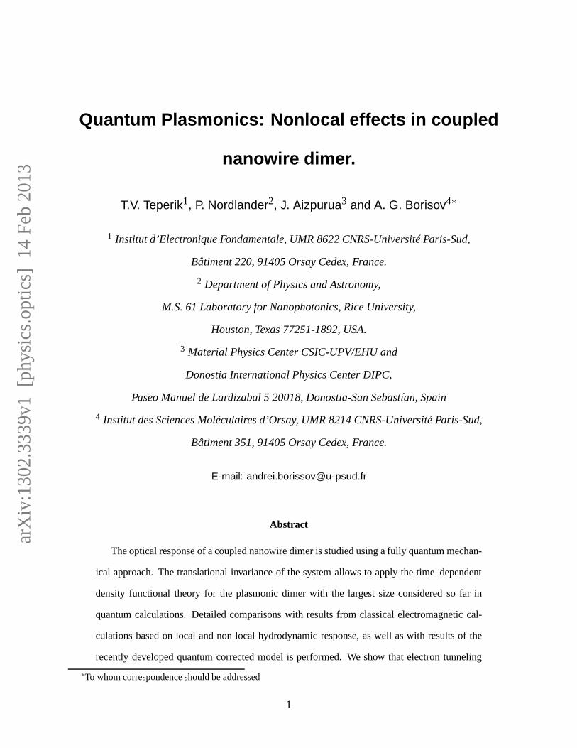
Quantum Plasmonics: Nonlocal effects in coupled
nanowire dimer.
T.V. Teperik1, P. Nordlander2, J. Aizpurua3 and A. G. Borisov4∗
1 Institut d’Electronique Fondamentale, UMR 8622 CNRS-Université Paris-Sud,
Bâtiment 220, 91405 Orsay Cedex, France.
2 Department of Physics and Astronomy,
M.S. 61 Laboratory for Nanophotonics, Rice University,
Houston, Texas 77251-1892, USA.
3 Material Physics Center CSIC-UPV/EHU and
Donostia International Physics Center DIPC,
Paseo Manuel de Lardizabal 5 20018, Donostia-San Sebastían, Spain
4 Institut des Sciences Moléculaires d’Orsay, UMR 8214 CNRS-Université Paris-Sud,
Bâtiment 351, 91405 Orsay Cedex, France.
E-mail: [email protected]
Abstract
The optical response of a coupled nanowire dimer is studied using a fully quantum mechan-
ical approach. The translational invariance of the system allows to apply the time–dependent
density functional theory for the plasmonic dimer with the largest size considered so far in
quantum calculations. Detailed comparisons with results from classical electromagnetic cal-
culations based on local and non local hydrodynamic response, as well as with results of the
recently developed quantum corrected model is performed. We show that electron tunneling
∗To whom correspondence should be addressed
1

and dynamical screening are the major nonlocal quantum effects determining the plasmonic
modes and field enhancement in the system. Account for the electron tunneling at small junc-
tion sizes allows semi-quantitative description of quantum results within classical framework.
We also discuss the shortcomings of classical treatments using non-local dielectric permittiv-
ities based on hydrodynamic models. Finally, the implications of the actual position of the
screening charge density for the plasmon ruler applications are demonstrated.
KEYWORDS Nanoparticle dimer, quantum plasmonics, field enhancement, plasmon ruler
In metal nanoparticles, collective excitation of the valence electrons induced by an incident
electromagnetic field, the localized plasmon, leads to plethora of optical phenomena of significant
current interest. For instance, strong plasmonic enhancement of the local fields1–5 opens a route
to numerous practical applications, such as surface enhanced Raman scattering (SERS),6–9 optical
nano-antennas10,11allowing, for example, the control of radiation from singlequantum emitters,12
or generation of extreme ultraviolet pulses by non-linear high harmonic generation.13 In nanopar-
ticle assemblies, the hybridization of plasmonic modes canserve for guiding of the propagating
fields,14,15as well as it offers a way for rational engineering of desiredoptical response and local
field profile.4 Not only light harvesting and sensing properties can be thusgreatly improved, but
also the specific geometry dependence of the optical response can be used as plasmon ruler to
determine the arrangement and nanoscale distances within chemical or biological species.4,16–21
Significant advances in fabrication and manipulation techniques allow nowadays for precise
control of the geometry of the structure.21–29 In particular, for nanoparticle assemblies the size of
the gap between the adjacent nanoparticles can be brought below one nanometer so that the electron
tunneling across the junction becomes possible. Thus, the plasmonic devices enter the quantum
regime which represents a significant challenge for available theoretical approaches. Indeed, most
of the descriptions of the optical response are based on the solution of the classical Maxwell equa-
tions where the nanoparticles are modeled with sharp surfaces and the quantum nature of electrons
forming the screening charge is neglected. Such effects as experimentally observed appearance
2
of the charge transfer plasmon for conductively coupled particles prior to direct contact,28,29 or
optical rectification23,30 can not be addressed within a classical framework. As shown with re-
cent quantum calculations28,31–34the main ingredients missing in the classical model are the spill
out of conduction electrons outside the nanoparticle surfaces, and the finite spatial profile of the
plasmon-induced screening charge. The use of a nonlocal dielectric functions2,35–43can account
for the latter effect, where the variation of electron density is smooth rather than infinitely sharp,
as assumed in the classical local approach. However, the spill out of electrons outside the nanopar-
ticle surfaces and associated tunneling across the narrow interparticle junctions requires special
treatment.
In this respect, the data available on the coupled nanoparticle dimer is quite revealing. This is
a prototypical system for plasmonic nanoparticle coupling, which has been extensively studied.2–4
Theoretical studies based on the solution of the classical Maxwell equations predict a discontin-
uous transition from the capacitively to conductively coupled particles. For vanishing junction
size, the fields in the junction diverge and the plasmon modesexperience diverging red shift as a
result of the interaction between high charge densities induced at the opposite sides of the junc-
tion.3–8,44–46The charge transfer plasmon appears abruptly after the conductive contact.45,47 The
nonlocal calculations based on the hydrodynamic model2,35,36,40–42have shown that because of the
finite spatial profile of the plasmon-induced screening charge, the fields in the junction stay finite
albeit large. The number of plasmon resonances and their frequency shift is much reduced com-
pared to classical predictions. On the other hand, it follows from the quantum treatments28,31–33
that for narrow junctions, electron tunneling can short circuit the junction and quench the plasmon-
induced field enhancement. The nanoparticles appear conductively connected prior to direct con-
tact, and the transition between the non-touching and conductive contact regimes is continuous. In
particular, the charge transfer plasmon associated with interparticle charge transfer48–52 progres-
sively emerges in the optical response of the system, as has been fully confirmed in recent experi-
ments.28,29These quantum effects could be reproduced with Quantum Corrected Model (QCM)33
that treats the junction between the nanoparticles as an effective medium allowing to account for
3
the quantum effects within the classical local Maxwell theory.28,29
Present situation is thus characterised by the experimental ability to create the structures with
sub-nanometer characteristic scales and several sometimes controversial theoretical approaches to
address the optical properties of such a nanostructures. While quantum calculations provide an
a priori exact answer to the problem, to date the application of rigorous quantum mechanical ap-
proaches to coupled plasmonic systems have been limited to rather small systems and are extremely
heavy numerically. It is thus of considerable interest to have a bench mark quantum results on pos-
sibly large realistic system of coupled plasmonic particles allowing detailed comparison between
full quantum and macroscopic Maxwell theories. This would allow to assess of the role of quan-
tum mechanical effects and of the possibility to account forthese effects in classical theory. In this
article which concerns a strongly coupled nanowire dimer, we offer such a comparison. We show
that the quantum mechanical results for the optical response of the system can be quantitatively
reproduced with simple models.Local classicaldescription of the system allows to account for the
interparticle tunneling through the narrow junction and for the actual location of the dynamically
induced screening charges.
Model and computational aspects
The system considered in this work consists of two identicalnanowires in vacuum. The nanowires
are infinitely extended alongz-axis as sketched in Fig. 1. Each nanowire has a circular cross-
section of diameterD. The nanowires are separated by a variable distanceS and the incident
light is polarized along the inter-particle axisx. Coupled nanowires and nanorods are often used
in SERS, nanoantenna, and plasmon guiding applications.3,4,10,11,20,24,53–57Thus, this system is
well characterized both from experimental and theoreticalpoint of view. Full numerical studies
based on the solution of the classical Maxwell equation havebeen performed,24,47,58–62as well as
semi-analytical studies based on transformation optics.40,41,63The system has also been investi-
gated using non-local hydrodynamic description.40–43 The high symmetry of the system with its
4

x
z
D
S
y
E
H
k
Figure 1: Sketch of geometry of the nanowire dimer. Two identical cylindrical nanowires areinfinite alongz-axis and have diameterD of the circular cross-section in the(x,y)- plane. Thenanowires are separated by the junction of widthS. The incident radiation is linearly polarisedwith electric field alongx-axis.
translational invariance along thez-axis allows us to address on the full quantum level the case of
the cylinders withD = 9.8 nm. To our knowledge this is the largest size of the plasmonic dimer
described so far within the time dependent density functional theory (TDDFT) framework.
For the nanowires we adopt the cylindrical jellium model (JM). Despite its simplicity, this
model captures the collective plasmonic modes of the conduction electrons and has demonstrated
its predictive power for quantum effects in nanoparticle dimers.28,29While obviously not providing
chemical accuracy, the JM is well suited for the descriptionof the nonlocal effects due to conduc-
tion electrons such as dynamical screening of external fieldand tunneling as we discuss below.
Along with the possibility to treat relatively large systemon a full quantum level, the JM model al-
lows for direct comparison between quantum and classical electromagnetic theory results. Indeed,
the physics underlying the Drude model for the metal response as well as the refinement of the
Drude model introduced by the nonlocal hydrodynamic model corresponds best to free electron
metals. For noble metals, such as silver and gold, the contribution of the localised d-electrons to
the screening would obscure the comparison.
Within the JM, the ionic cores of the nanowire atoms are represented with uniform back-
5

ground charge densityn0 =(4π
3 r3s
)−1. The screening radiusrs is set equal to 4 a0 (Bohr radius
a0=0.053 nm) corresponding to Na metal. Sodium is a prototype system for which the JM per-
forms particularly well in description of the finite size non-local effects on optical properties.64
It should be emphasized that the qualitative conclusions drawn in this work are robust and inde-
pendent of the particular choice of density parameter. Eachof nanowires is characterised by the
number of electronsNe per unit length so that from the charge neutrality the nanowire diameter
is D = 2√
4Ner3s/3. The circle of diameterD provides the position of the jellium edge separating
uniform positive background from the vacuum. The jellium edge is located at half a lattice con-
stanta (a = 4.23 Å for Na) in front of the last atomic plane at the surface. Wehave performed
calculations forNe = 40 andNe = 100 withD40 = 6.2 nm andD100= 9.8 nm respectively. The
Fermi energy in both cases is at 2.9 eV below the vacuum level.
The quantum calculations of the absorption cross-section are based on the Kohn-Sham (KS)
scheme of the time-dependent density functional theory (TDDFT).65 We use the adiabatic lo-
cal density approximation (ALDA) with the exchange-correlation functional of Gunnarson and
Lundqvist.66 Retardation effects can be neglected due to the small size ofthe system. Extended
description of present numerical implementation can be found in Ref.32 Therefore we only dis-
cuss here specific aspects linked with present work on interacting nanowires. In brief, the Kohn-
Sham orbitals of the ground state of interacting dimerψ j(x,y) are obtained from these of non-
interacting distant cylinders by adiabatically reducing the separation. Theψ j(x,y) are discretized
on the equidistant mesh in cartesian coordinates, and the time dependent Kohn-Sham equations
i∂Ψ j(x,y, t)
∂ t=
(
− ∆2m
+Veff(x,y, t; [n])
)
Ψ j(x,y, t) (1)
are then solved with initial conditionsΨ j(x,y, t = 0) = ψ j(x,y). In Eq. (1)m is the free electron
mass, and∆ = ∂ 2/∂x2+∂ 2/∂y2. The effective potential of the systemVeff depends on the electron
6

densityn(x,y, t) given by:
n(x,y, t) = 2 ∑j∈occ.
χ j∣
∣Ψ j(x,y, t)∣
∣
2. (2)
The sum runs over occupied states, the factor 2 results from the spin degeneracy, andχ j is the
number of electronic states associated withz-motion along the nanowire.
χ j =1π
√
2(EF −E j) , (3)
whereEF is the Fermi energy, andE j is the energy of theψ j(x,y) orbital.
The dipole absorption cross-section per unit length is calculated from the density dynamics
induced by impulsive perturbation as:σabs(ω) = 4πωc Imα(ω), with α(ω) being the dipolar po-
larizability (per unit length) of the system, andc - speed of light in vacuum. In order to analyse the
temporal evolution of the system corresponding to the excitation of the given plasmonic resonance
we perform the TDDFT calculations for the nanowire dimer subjected to an incidentx-polarized
laser pulse. Electric field of the pulse is given byEL(t)=E0exp[
−( t−T
0.2T
)2]
cosΩt. The frequency
of the pulseΩ is set resonant with studied plasmonic mode. The duration ofthe pulseT (typically
50 fs) is large enough for the narrow spectral width. The amplitude E0 is any small number to
guarantee the linear response regime.32 The snapshots of the induced densities, currents and fields
presented lower in this paper are extracted att ∼ T/2.
The classical electromagnetic calculations of the absorption cross-section have been performed
with Comsol Multiphysics package, (version 4.2a, www.comsol.com). Local, nonlocal, and quan-
tum corrected model description of the dielectric properties of the system were used. It is note-
worthy that because of the small size of the plasmonic dimer the absorption cross-section closely
correspond to extinction cross-section in this case.
Within the local classical approach the dielectric constant of the nanowires is described with
Drude model, which is a good approximation for the free electron metal as sodium considered in
7
this work.
ε(ω) = 1−ω2
p
ω(ω + iγ), (4)
whereωp is the bulk plasma frequency given byωp =√
4πn0/m= 5.89 eV, andγ accounts for
the damping.
The quantum corrected model (QCM) allows to introduce the tunneling effect into the classical
Maxwell equations. We use the local approach where the nanowires are described with Drude
model Eq. 4, and the tunneling across the vacuum gap between the nanowires is accounted for by
filling the junction with an effective dielectric medium.33 It is described with the Drude model,
similar to Eq. 4:
εeff(y,S,ω) = 1−ω2
p
ω(ω + iγeff(y,S)). (5)
The effective dampingγeff models transition from resistive (largeS) to conductive (smallS) char-
acter of the junction. Thus, it acquires a dependence on the separation distanceSandy-coordinate.
For very largeSthe QCM is exactly equivalent to local classical approach. No tunneling is possible
and the vacuum gap limit is retrieved withεeff(y,S,ω) = 1. In this work we use exactly the same
parametrization ofεeff as in the earlier publication, where the QCM is introduced and described in
great detail.33
Within the non-local hydrodynamic description the transverse component of the permittivity
tensor is given by Eq. (4), and the longitudinal component acquires the wave vectork dependence:
εL(ω) = 1−ω2
p
ω(ω + iγ)−β 2k2 . (6)
The β parameter is given byβ =√
3/5vF .2,35,36,40–42In the present case, the Fermi velocity of
conduction electronsvF = 3√
3π2n0/m= 1.05 106 m/s, resulting inβ = 0.81 106 m/s. Provided
transverse and the longitudinal components of the permittivity tensor the absorption cross-section
is calculated with numerical approach as recently implemented by G. Toscano and coworkers
within the Comsol Multiphysics package.42
8

D = 6.2 nm D = 9.8 nm
Figure 2: Absorption cross sectionσ for the single jellium nanowire of the diameterD = 6.2 nm(left) andD = 9.8 nm (right). Results are shown as function of the frequencyω of the incidentradiation. The incoming field is thex-polarised plane wave. The TDDFT calculations are com-pared with results of the classical electromagnetic calculations using local (Drude) and nonlocalhydrodynamic response. (See the legend for definition of differnt symbols used in the figure).
Results and discussion
Individual Nanowire
We first characterize the linear optical response of individual nanowire. In Fig. 2 we show the
dipole absorption cross-sectionσ calculated with full quantum TDDFT method and with classical
local Drude and non-local hydrodynamic approaches. The classical local approach with the Drude
model given by Eq. 4 for the permittivity of the nanowire leads to the dipole resonance located at
surface plasmon frequencyωsp= ωp/√
2= 4.16 eV irrespectively of the nanowire diameter. We
find that the absolute value ofσ and the width of the resonance as calculated with TDDFT is best
reproduced with damping parameterγ = 0.275 eV for theD = 6.2 nm nanowire, andγ = 0.247 eV
for theD = 9.8 nm nanowire. The smaller damping obtained for larger nanowire indicates smaller
decay due to surface scattering. Indeed, the surface scattering contribution to the damping can
be expressed asγS = AvF/Rcl,67 whereRcl = D/2 is the cylinder radius, andA is the system-
dependent parameter. The calculated change of the damping is consistent withA= 0.5 in accord
with available experimental and theoretical results for alkali clusters.68,69 Obviously, through the
9

width of the single wire resonance the quantum size effects would affect the optical response of
the nanowire dimer.70
The dipole resonance calculated with TDDFT isred shiftedfrom the classicalωsp value but
approachesωsp for increasing size of the system. For theD = 6.2 nm nanowire, the resonance is
at ω = 4.027 eV, and it is atω = 4.072 eV for theD = 9.8 nm nanowire. Thus, present TDDFT
results for cylindrical nanowire show the same trends as studied in detail for spherical alkali metal
clusters.64,71–73The non-local effect at the origin of the red shift of the plasmon resonance is linked
with dynamical screening of the fields by conduction electrons. The dipole resonance frequency
can be found from:72–75
ω/ωsp= 1−Re[d(ωsp)]/Rcl+O(R−2cl ). (7)
The real part of Feibelman’s parameterRe[d(ω)] gives the position of the centroid of the induced
charge density.76–78When measured from the jellium edge,Re[d(ωsp)] is positive for alkali metals,
i.e. the screening charge is shifted into the vacuum becauseof the spill out of the conduction
electrons outside the metal. From the calculated resonancefrequency we obtainRe[d(ωsp)] = 1 Å
in agreement with earlier calculations and experiment.73,76,77 Importantly, for the noble metals
such as Au and Ag the final size effects lead to theblue shiftof the dipole plasmon resonance.29,79
The difference between alkali and noble metals is the localised d-electron contribution to the total
screening in the latter case.75,78–81When the d-electron contribution is accounted for,Re[d(ω)]
turns negative indicating that screening charge is predominantly induced inside metal.75,79,80
For the small diameter nanowireD = 6.2 nm, finite size effects appear in the TDDFT calcu-
lations not only in the form of red shifts and line width changes, but also as clearly observable
structures in the frequency dependence of the absorption cross section. These structures arise
from the strong coupling of collective plasmon- and single electron-hole excitations. For large
diameter nanowires, finite size effects become smaller and the plasmon resonance is much better
defined. The TDDFT results also show shallow resonance in theoptical absorption cross section
10

at ω = 4.6 eV associated with a multipole plasmon (MP).82–84 The resonant frequency obtained
with TDDFT is in good agreement with experimental data.82,84The density oscillations of the MP
proceed within the layer of the spilled out charge as obviously can not be captured within the local
classical theory.
Finally, the green dotted lines in Fig. 2 show the absorptioncross-section calculated with the
classical non-local hydrodynamic model (NLHD).42 In contrast to the TDDFT result and exper-
imental data on alkali clusters,72,73 the NLHD model predicts a blue shift of the dipole plasmon
frequency fromωsp value. The reason for this is that independent of the metal, the plasmon-
induced charges in NLHD are localized within the layer of thethicknessβ/ωp below the metal
surface.41 Thus, the effectiveRe[dNLHD(ω)] is always negative leading to the blue shift of the
localised plasmon78 in contradiction with the spill out effect known for alkali metals. However,
negativeRe[dNLHD(ω)] inherent to NLHD description of conduction electrons and sothe blue
shift of the localised plasmon qualitatively coincides with full quantum result determined by the
d-electron screening for the noble metals.75–82
Coupled Nanowires
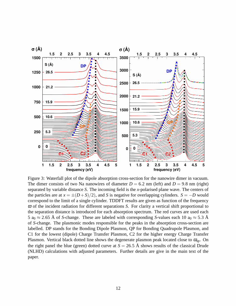
In Fig. 3 we show waterfall plots of the dipole absorption cross-section of theD = 6.2 nm and
D = 9.8 nm nanowire dimers calculated with TDDFT. The results are presented as function of the
frequency of the incident radiation for different widthsS of the junction. The calculations have
been performed for both positive and negativeS, where the latter means a geometrical overlap
of the nanowires. TheS= 0 case corresponds to the kissing cylinders40,41 with touching jellium
edges where the distance between the topmost atomic planes equals to the interlayer spacing, i.e.
a continuous solid is formed at the contact point.
For large positive separations the non-local effects including electron tunneling across the junc-
tion are small, and the TDDFT results agree with earlier classical calculations41,41,47,58,59(See also
Fig. 5). At S= 26.5 Å the absorption spectrum is dominated by two resonant structures. First is
the bonding dipole plasmon (DP) indicated with blue dotted line in Figure. It is formed from
11
1 1.5 2 2.5 3 3.5 4 4.5 5frequency (eV)
1 1.5 2 2.5 3 3.5 4 4.5 5frequency (eV)
1.5 2 2.5 3 3.5 4 4.5 1.5 2 2.5 3 3.5 4 4.5 3500
3000
2500
2000
1500
1000
500
0
1500
1250
1000
750
500
250
0
σσσσ (Å) σσσσ (Å)
26.5
21.2
15.9
10.6
5.3
0
26.5
21.2
15.9
10.6
5.3
0
S (Å)
S (Å)
DPDP
QPQP
C1 C1 C2C2
Figure 3: Waterfall plot of the dipole absorption cross-section for the nanowire dimer in vacuum.The dimer consists of two Na nanowires of diameterD = 6.2 nm (left) andD = 9.8 nm (right)separated by variable distanceS. The incoming field is thex-polarised plane wave. The centers ofthe particles are atx= ±(D+S)/2), andS is negative for overlapping cylinders.S= −D wouldcorrespond to the limit of a single cylinder. TDDFT results are given as function of the frequencyω of the incident radiation for different separationsS. For clarity a vertical shift proportional tothe separation distance is introduced for each absorption spectrum. The red curves are used each5 a0 ≈ 2.65 Å of S-change. These are labeled with correspondingS-values each 10 a0 ≈ 5.3 Åof S-change. The plasmonic modes responsible for the peaks in the absorption cross-section arelabelled. DP stands for the Bonding Dipole Plasmon, QP for Bonding Quadrupole Plasmon, andC1 for the lowest (dipole) Charge Transfer Plasmon, C2 for the higher energy Charge TransferPlasmon. Vertical black dotted line shows the degenerate plasmon peak located close toωsp. Onthe right panel the blue (green) dotted curve atS= 26.5 Å shows results of the classical Drude(NLHD) calculations with adjusted parameters. Further details are give in the main text of thepaper.
12

hybridization of the dipole plasmon modes of the individualnanowires. The second resonance
indicated with black dotted line is formed by bonding quadrupole (QP) plasmon degenerated with
higher order modes. It is slightly red shifted with respect to the surface plasmon frequencyωsp.
At S→ ∞, the DP merges into the degenerate mode and the spectrum evolves into that of the indi-
vidual nanowire. As the junction widthSdecreases, the DP shifts to lower frequencies because of
the attractive interaction between the charges of oppositesign across the junction. Along with red
shift of the DP, the QP (orange dotted line in Figure) splits from the degenerate mode, and shows
the red shift with decreasingS.
Despite the overall similarity of the results obtained withsmaller and larger diameter nanowires
there are some notable differences primarily caused by finite size effect. The resonances are much
better defined for the largerD=9.8 nm nanowire. In this case the width of the resonances is smaller
and the structures due to the interaction between the plasmon and electron-hole pair excitations
disappear. ForD = 6.2 nm nanowire, this interaction can even split the single plasmon peak into
several lines. The red shift of the DP and QP modes with decreasing S is more pronounced for
the D = 9.8 nm nanowire dimer. This is because of the scale (S/D) invariance of the plasmonic
properties of nanostructure in the quasistatic limit.
For junction widths below∼ 7 Å, electron tunneling across the junction becomes important.
The results obtained here for the nanowire dimer have much incommon with those reported in
quantum studies of touching spherical nanospheres,31–33 and in recent experiments.28,29 The DP
resonance progressively disappears and the charge transfer plasmon mode (C1) emerges prior to
the direct contact between the nanoparticles. C1 appears asa broad shallow low-frequency peak
at positiveS≃ 1.5 Å, and evolves into a well–defined resonance atS< 0. Similarly, because of
electron tunneling, the QP mode continuously evolves into ahigher order charge transfer plasmon
mode C2 before direct contact between the nanowires. Thus, already at positiveS the nanowires
appear conductively connected showing characteristic charge transfer plasmon modes.45,48–51For
a dimer with well established conductive contact, the C1 andC2 modes experience a blue shift as
also reported in classical calculations.45,63
13

-189 -151 -113 -75 -38 0 38 75 113 151 189
-113
-75
-38
0
38
75
113
-113
-75
-38
0
38
75
113
-189 -151 -113 -75 -38 0 38 75 113 151 189
-189 -151 -113 -75 -38 0 38 75 113 151 189
∆∆∆∆n Jx
7.95
Å2.
65 Å
0-
2.65
Å
-189 -151 -113 -75 -38 0 38 75 113 151 189
∆∆∆∆n Ex
∆∆∆∆n Ex Jx
∆∆∆∆n Ex Jx
Ex/Emax
cu
rre
nt
5.3 Å2.65 Å1.06 Å0
(b)(a)
(d)(c)
(f)(e) (g)
(i)(h) (j)
(k)
Figure 4: Panels (a)-(k) Detailed analysis of the plasmon dynamics in the coupled Na nanowiresof diameterD = 9.8 nm. The incidentx-polarised laser pulse is at resonance with lowest (dipoleplasmon mode of the system). Panels (a)-(j) present the snapshots of the induced charge density∆n, current densityJx, and fieldEx for different junction widthsSas indicated to the left of eachrow. The induced currents and fields are measured along interparticlex-axis. Positive (negative)values correspond to red (blue) color code. The induced densities are shown at the instant of timecorresponding to the maximum dipole moment of the dimer. Theinduced currents and fields areshown at the instants of time when the induced fields in the junction reach maximum. Panel (k):Conductivity analysis. The currentJx measured onx-axis in the middle of the junction is plottedas a function of the normalized electric field at the same position. Different colors correspond todifferent separationsSas explained in the insert.
14
To obtain further insights into the effect of the tunneling through the junction we have calcu-
lated the electron density dynamics in the plasmonic dimer subjected to an incidentx-polarized
laser pulse resonant with lower (DP or C1) plasmonic modes. The panels (a)–(j) of Fig. 4 show
snapshots of the induced charge density∆n, andx-component of the current densityJx, and field
Ex for different junction widthsS. Results are given for the case ofD = 9.8 nm nanowires. The in-
duced densities are shown at the instant of time corresponding to the maximum dipole moment of
the dimer. The currents and fields are shown at the instant of time corresponding to the maximum
induced field in the junction.
For large separationS= 7.95 Å the maximum induced dipole corresponds to the in–phase
dipole polarisation of each nanocylinder expected for the DP mode. High charge densities are in-
duced at the surfaces facing the junction resulting in largeelectric field enhancement|E0/Ein| ∼ 80.
Here,Ein is the amplitude of the incident field andE0 is the amplitude of the field measured at the
x-axis in the middle of the junction. The structure of the induced charges and fields are similar to
previous classical results for coupled cylinders41,47,58,59and also resembles much to the case of
metal sphere dimer.45 The probability of tunnelling between nanowires is negligible and no current
flows across the junction. Note that the maximum dipole polarisation corresponds to the instant of
time when the maximum charge separation has occurred and thecurrents inside nanoparticles are
minimal. For the reduced widthS= 2.65 Å, very similar profiles for induced densities and fields
are obtained. Therefore, we do not showEx but focus on the induced current. The junction width is
now sufficiently small to allow weak electron tunnelling between the nanoparticles. Large optical
field in the junction acts as large BIAS in the scanning tunneling microscope causing tunneling cur-
rent across the junction.33 Thus, the junction shows theresistivecharacter with maximum current
between nanowires reached at the maximum field and consequently at maximum induced dipole.
Further reduction of the separationS increases the tunneling probability and short circuits the
junction. When conductive contact is formed, the DP mode disappears and the C1 mode emerges
in the absorption spectrum. Panels (e) and (h) Fig. 4 show theinduced charges forS= 0 and
S= −2.65 Å, respectively. The results are very similar, i.e. already for theS= 0 case of kissing
15
cylinders the charge transfer plasmon mode is well developed (see also Fig. 3, and Fig. 5). The
maximum dipole moment of the dimer corresponds to the oppositely charged nanowires. Max-
imum currents and fields [panels (f), (g), (i), (j)] are reached when the total dipole moment of
the system is minimum (compare withS= 2.65 Å case). Precisely, this is large current flowing
trough the entire system that builds the dipole polarisation with opposite charges at left and right
nanowires consistent with resonant excitation of the C1 mode. The field enhancement is about 30
for bothS= 0 andS= −2.65 Å separations. However, the fields are screened at the center of the
junction, and the maximum fields are located at its sides. This is similar to the classical result for
the overlapping cylinders.63
Panel (k) of Fig. 4 provides further analysis for the evolution from resistive to conductive
character of the junction with decreasingS. The currentJx(t) on thex-axis at the middle of the
junction between the nanowires is shown as a function of the field Ex(t) at the same location. At
large separations, the linear relationJx(t) = gEx(t) between the current and the local field shows
that the junction is resistive. The increase of the slopeg whenS is reduced fromS= 5.3 Å to
S= 2.65 Å is because of the increase of the tunneling probability.ForS= 1.06 Å andS= 0 Å the
Ex(t) andJx(t) acquire a relative phase. Since the field envelope of the incident pulse grows in time
for the time interval shown in Fig. 4(k), the clock-wise rotation of theJx(t)[Ex(t)] curve implies
that the current is retarded with respect to the field. The junction becomes conductive which is
particularly apparent forS= 0.
The TDDFT results show that for small junction widths the optical response is determined
by electron tunneling. For large width of the junction the tunneling is negligible. Each cylinder
responds on the self consistent field created by the incidentradiation and the neighbour. The
effects of nonlocal screening discussed for the single cylinder shoulda priori influence the optical
response of the dimer as suggested with NLHD calculations40–43 and as inherently build in the
TDDFT results. While the effect of tunneling is clearly seenwith TDDFT calculations, revealing
the role of the nonlocal screening requires comparison withclassical results, in particular for the
energies of the plasmonic modes. In this respect, present system offers a unique opportunity to test
16

10 20 30 40
separation
0 20 40 60 80 100 120
0 5 10 15 20 25 30 35 40
separation (a.u.)
0 20 40 60 80 100120
TDDFT QCM Classicalσσσσ (Å)
1000
500
0
S (Å)
10.6
5.3
0
-5.31.5 2.0 2.5 3.0 3.5 4.0 4.5
frequency (eV)
S (Å)
10.6
5.3
0
-5.31.5 2.0 2.5 3.0 3.5 4.0 4.5
frequency (eV)1.5 2.0 2.5 3.0 3.5 4.0 4.5
frequency (eV)
0 5 10 15 20 25 30 35 40
separation (a.u.)
0 20 40 60 80
0 5.3 10.6 15.9separation (Å)
ωωωω (eV)
4
3
2
10 5 10 15 20 25 30 35 40
separation (a.u.)
20 40 60 80
0 5.3 10.6 15.9separation (Å)
0 5.3 10.6 15.9separation (Å)
TDDFT QCM Classical
DPDPQP QP
C1 C2 C1C2
1.5 2.0 2.5 3.0 3.5 4.0 4.5frequency (eV)
Nonlocal
0 5.3 10.6 15.9separation (Å)
S (Å)
10.6
5.3
0
-5.3
Nonlocal
DP
QP
DP
QP
C1 C2
Figure 5: Comparison of the optical properties of a nanowiredimer obtained with the full TDDFTcalculations, with the quantum corrected model (QCM), witha classical Drude electromagneticcalculations (Classical), and with calculations based on the nonlocal hydrodynamic model (Non-local). The dimer consists of twoD = 9.8 nm Na nanowires in vacuum. The incoming plane waveis polarized along the dimer axisx. Upper panels: Waterfall plots of the dipole absorption cross-section as function of the width of the junctionS. Red curves correspond to separation distancesof S= −5.3 Å, −2.65 Å, 0 Å, 2.65 Å, 5.3 Å, 7.95 Å, and 10.6 Å. For further details see captionof Fig.3 Lower panels: Color plots of the local field enhancement at the center of the junction forpositive separations. Results are shown as function of the frequencyω of the incident radiationand separation distanceS. The color code is explained at the bottom of the corresponding panels.
17
the validity of different classical models against full quantum results for relatively large system,
with fully developed plasmonic modes, and with dielectric properties well described within free
electron approximation. The rest of the paper is devoted to quantum vs classical comparison with
particular focus on possibility to account for quantum effects within classical approach.
Quantum vs classcal approaches
Fig. 5 shows the present TDDFT results, the QCM results, results from classical calculations based
on the Drude description of Na dielectric function, and results of the NLHD calculations. Waterfall
plots of the absorption cross-section (upper panels) and contour plots of the field enhancement on
thex-axis at the middle of the junction are presented as functionof the frequency of the incoming
plane wave and of the junction widthS. Since for the individual nanowire TDDFT gives a red
shift of the dipole plasmon resonance from the classicalωsp position, while NLHD leads to a blue
shift (Fig. 2), we adjust the parameters of different models. For the sake of comparison of the
junction width dependence we enforce an agreement between the TDDFT, QCM, classical Drude,
and NLHD at the largestScalculated here with TDDFT,S= 26.5 Å (see Fig. 3). For theD = 9.8
nm nanowire dimer we have used plasma frequencyωp = 5.8 eV and dampingγ = 0.247 eV
in the QCM and classical Drude calculations. Thus, only small correction to the bulk plasma
frequency (nominal value 5.89 eV) is required in this case. The NLHD model needs for much
larger correction to compensate for the blue shift inherentto this treatment. We usedωp = 5.5 eV
andγ = 0.16 eV. Adjustment of the nonlocality parameterβ is also possible, but then the model
looses its predictive power. Indeed, as far adjustment is limited toωp andγ parameters, the finite
size effects and so the need for correction will disappear with increasing size of the nanoobjects.
The main features of the quantum results have been discussedin connection with Fig. 3 so here
we will focus on comparisons between different model approaches. As follows from Fig. 5, the
QCM does an excellent job in describing the TDDFT results over the entire range of separations
S addressed here. The important features such as: the number of resonances; their distance de-
pendence; the transition from the separated to conductively coupled regime are well reproduced.
18

In particular, in sheer contrast with classical theory41,45,47,58,59the change of the spectrum at the
moment of contact is progressive and fields at the middle of the junction are quenched, not diverg-
ing with decreasing junction size. Besides qualitative aspects, we find that the TDDFT and QCM
agree semi-quantitatively as is further stressed in Fig. 6.This figure zooms into the most delicate
interaction regime corresponding to the transition from the separate to overlapping nanowires.
By construction of QCM, it is equivalent to the classical local Drude description for large
positiveSwhere tunneling is negligible. The good agreement with TDDFT data suggests that the
pure local classical description is reasonable for a largeS. At the same time the classical description
fails at smallS∼ 5 Å, i.e. typically at two lattice constants between surfaceatomic planes that
define the junction.29 The accumulation of charges on the opposite sides of the junction leads
to exaggerated coupling between nanowires resulting in diverging fields and too large number of
resonances. Similarly, for negativeS, the sharp edges of the junction, which are otherwise smeared
out by the electron tunneling also result in too many hybridized resonances.33
The NLHD description is free from theS= 0 divergence problem.40,41 The number of reso-
nances remains small and the fields in the middle of the junction stay finite albeit too large. This
can be easily understood thanks to the elegant transformation optics approach developed for in-
teracting cylinders by Fernández-Domínguez and coworkers.41 At positiveSan analytic solution
is found which depends on the renormalised parameterS≃ S+ 2δ , whereδ ≃ β/ωp (1 Å in
the present case). The physics behind this shift is the localisation of the plasmon-induced charge
below the surface as inherent for the NLHD model. As we discussed for the single cylinder,
in terms of the dynamical screening theory,δ is equivalent to an effective Feibelman parameter
δ =−Re[dNLHD(ω)]. Thus, even forS= 0, the induced charges at the opposite sides of the junc-
tion are actually separated by a finite distance 2δ . However, since the tunneling is not accounted
for, the NLHD description fails to reproduce the quenching of the field enhancement at the middle
of the junction for small positiveS. The NLHD also fails to smoothen out the transition from sep-
arated to overlapping regimes and gives an abrupt nonphysical transition. The number of modes is
smaller than in the classical Drude description, but still larger than what is obtained in TDDFT or
19

σσσσ (Å)
300
250
200
150
100
50
0
1.4 1.8 2.2 2.6 3.0 3.4frequency (eV)
1.4 1.8 2.2 2.6 3.0 3.4frequency (eV)
TDDFT QCM
DP
C1
DP
C1
1.4 1.8 2.2 2.6 3.0 3.4 1.4 1.8 2.2 2.6 3.0 3.4
4.24
3.18
2.12
1.06
0.0
-1.06
-2.12
S (Å)
σσσσ (Å)
300
250
200
150
100
50
0
Figure 6: Detailed comparison between TDDFT and QCM calculations. The dipole absorptioncross-section of theD= 9.8 nm Na nanowire dimer is shown for small separationsScorrespondingto the strong tunneling regime and transition from separated to conductively coupled nanowires.The frequency range is zoomed at the transition from the bonding dipole (DP) to the lowest chargetransfer (C1) plasmon. Waterfall plots of the optical absorption cross-section are shown for theseparation distances changing fromS= −2.65 Å (lowest blue line) toS= 4.77 Å (upper blackline) in steps of 1a0 (0.53 Å). For further details see caption of Fig. 3.
20

QCM calculations.
Our final remark concerns the QP plasmon that evolves into theC2 charge transfer mode for
negativeS. The associated resonances are much less pronounced in the TDDFT cross-section
compared to model approaches. One possible reason is finite size effect, where the the system size
is not large enough for the corresponding density oscillations to be completely formed. However,
the similarity between the TDDFT results forD = 6.2 nm andD = 9.8 nm nanowire dimers as
shown in Fig. 3 suggests that this quantum size effect is small. We thus tentatively attribute the
weaker high order resonances as obtained in TDDFT to the effect of the smearing of the induced
surface charge densities. Thisa priori reduces the coupling between the dipole and higher order
modes and consequently the intensity of the QP resonance in the dipole absorption cross-section.
Dynamic screening
With results shown in the previous Subsection, tunneling determines the optical properties of the
system at small junction widths. For large widthS tunneling is absent and nonlocal dynamic
screening influences the optical properties. Similar to thecase of the individual nanowire, the
major nonlocal effect is the red shift of the frequency of thebonding dipole plasmon as compared
to the classical prediction. However, for the dimer, this effect is much stronger, and does not
disappear with increasing radius of nanoparticle.
Fig. 7 presents the analysis of the role played by dynamic screening in determining the fre-
quency of the bonding dipole plasmon. Panel (a) gives schematic representation of the location
of plasmon induced screening charges in the junction of width S. Within the local classical ap-
proach the screening charges are localised at geometrical surfaces of the cylinders separated byS.
We recall that we use the definition of the geometrical surface such that it coincides with jellium
edge. Within TDDFT, the real part of the centroid of the induced charge densityRe[d(ω)] corre-
sponds to the position of the plasmon-induced surface charges with respect to the jellium edge of
each cylinder.74–78,80,82For the present case of sodium nanowires,Re[d(ω)] is positive≈ 0.9 Å
in the frequency range of interest.77 This means that the screening charge is shifted by 0.9 Å into
21

(b)
(c) (d)
S
S-2Re(d)
S+2δδδδ
(a)
Figure 7: Dynamic screening. (a) Schematic representationof the location of plasmon inducedscreening charges in the junction. Within the local classical approach the screening charges are atgeometrical surfaces of the cylinders (here equivalent to the jellium edges) separated by the junc-tion of width S. Within the TDDFT, the centroids of the screening charges (red areas) are locatedat Re[d(ω)] in front of the jellium edges and separated byS− 2Re[d(ω)]. In NLHD approachthe centroids of the screening charges (blue areas) are located at distanceδ below the geometricalsurface and separated byS+2δ . (b) Energy of the dipole plasmon resonance as function of thejunction widthS. Dots: TDDFT results obtained for nanowire dimers formed byD = 6.2 nm andD = 9.8 nm nanowires (see the legend). Solid and dashed lines show results of classical Drudecalculations forD = 6.2 nm (blue) andD = 9.8 nm (red) dimers. Dashed lines: separationS ismeasured between the jellium edges. Solid lines: separation S is measured between the centroidsof the induced charges. For more details see the main text. (c) Energy of the dipole plasmonresonance as function of the junction widthS. Dots: TDDFT results obtained forD = 9.8 nmnanowire dimer. Solid and dashed red lines show results of classical Drude calculations [same as(b)]. Dashed and dotted gray lines show results of NLHD calculations. Dashed line: separationSismeasured between the jellium edges. Dotted line: separation S is measured between the centroidsof the induced charges. (d) Same as (b), but results are shownas function of the scaled separationS/Rcl, whereRcl = D/2 is the nanowire radius.
22

the vacuum and located at≈ 3 Å outside the surface atomic plane of the nanoparticle. Thedis-
tance between the plasmon induced charges across the junction is thusΣ = S−2Re[d(ω)]. As to
the NLHD approach, with present choice of the non–locality parameterβ it places the screening
charges atδ = 1 Å inside the geometrical surface. Thus, within the NLHD approach the screening
charges are separated by the distanceS+2δ .
This insight provides an explanation for the junction widthdependence of the DP modes shown
in Fig. 7(b) for two different nanowire dimers. While the overall agreement between the classical
Drude (dashed lines) and the TDDFT (dots) calculations is good, the TDDFT result is system-
atically redshifted. The difference is increasing with decreasingS indicating that the classical
calculations underestimate the coupling between the dipole plasmons localized on each nanowire.
Our finding that the plasmon-induced charges in the TDDFT calculations are outside the nanopar-
ticle surfaces explains this effect. Indeed, the actual energy of the DP is given by the interaction
between the screening charges across the junction. Thus, the TDDFT data obtained for junction
width Sshould be compared with classical results calculated forΣ = S−2Re[d(ω)]. If the DP dis-
persion is plotted as a function of effective junction widthgiven by the distance between plasmon
induced screening charges, the agreement between TDDFT andthe classical simulations becomes
excellent. We note in passing that the step-structure of theTDDFT data for the smallerD = 6.2 nm
dimer steams from the strong coupling between plasmon and electron-hole pair excitations.
A similar analysis can be performed for the NLHD model calculations shown in Fig. 7(c) for
the case ofD = 9.8 nm nanowire dimer. The NLHD results appear at even higher frequencies than
the classical Drude calculations, in even stronger disagreement with the TDDFT than the classical
model. The explanation for this is that NLHD artificially places the plasmon–induced screening
charges at a position∼ δ = 1 Å inside the metal surface. Thus, the separation between screening
chargesS+2δ in the NLHD model is larger than separationS in pure local theory, and too large
compared to the quantum resultΣ = S−2Re[d(ω)]. This decreases the interaction and results in
blue shifted DP modes compared to the classical model and TDDFT. If the DP dispersion is plotted
as a function of effective junction width, agreement between NLHD, classical Drude, and TDDFT
23

results is obtained.
The above results show that the TDDFT dispersion of the DP canbe fully retrieved with local
classical calculations. The main issue here is the size of the junction for which the calculations
have to be performed. For geometry of the nanostructure, it seems convenient to define the surfaces
of the objects as given by the jellium edges. In this case the width S= 0 of the junction would
correspond to continuous solid formed at the contact point,which is physically sound. On the
other hand, classical calculations have to be performed forthe effective junction width given by
the actual separation between the screening charges. Theseconclusions have direct implications
for the ultimate limit of resolution of plasmonic rulers.18
For the free-electron Na surface, the screening charges arelocated at approximately 0.9 Å (3 Å)
outside the jellium edge (surface atomic layer) meaning that for a Na–Na junction, the effective
junction width would be 1.8 Å (6 Å) smaller than the physical junction width measured between
the jellium edges (surface atomic planes). This conclusionholds not only for the nanowire case
considered here, but for any junctions between Na surfaces.For silver and gold, analysis of the data
on the blue shift of the dipole plasmon resonance in small clusters29,75,79,85,86with Eq. 7 places the
effective screening charges inside the jellium edge at 1.5÷0.85 Å for silver, and at approximately
1.5 Å for gold. Therefore, for an Ag–Ag (Au–Au) junctions, the effective junction width would be
by 1.7÷3 Å (∼ 3 Å) larger than the physical junction width measured between the jellium edges
and close to the junction width masured between the surface atomic planes.
The use of the plasmon ruler relies on the universal dependence of the DP frequency on the
scaled separation.16,17 In Fig. 7(d) we show the TDDFT and classical results for the DPfrequency
of the D = 6.2 nm andD = 9.8 nm nanowire dimers as function of the scaled separationS/Rcl.
The TDDFT data for both nanowire dimer sizes nearly falls on the unique curve provided that the
separationsSare sufficiently large that no tunneling occurs. This holds for Slarger than typically 2
lattice constants between surface atomic planes, which sets lower bound for the distances that can
be actually measured with plasmon ruler.
24

Summary and Conclusions
In conclusion, we have presented fully quantum mechanical study of the optical response of the
plasmonic dimer formed by realistic size cylindrical nanowires. This system is also representative
of interacting nanorods and is of relevance for SERS, plasmon ruler, and plasmon transport appli-
cations. Translational invariance allows to apply the time–dependent density functional theory for
the plasmonic dimer of largest size considered so far in quantum calculations.
We considered nanowires made of Sodium which is a prototype for free-electron metal so
that jellium model applies. The free-electron character ofNa valence electrons implies that its
permittivity can be well described with Drude model, as wellas it is consistent with approximations
behind the hydrodynamic approach to model the nonlocal character of the dielectric function.
Thus, this is the system of choice allowing to set the full quantum TDDFT benchmark results, and
to use these results to test different theoretical approaches addressing plasmonic response of the
strongly coupled objects. This was one of the central goals of the present work.
We have found that for the small junction widths, the opticalresponse is determined by the
quantum tunneling of conduction electrons across the potential barrier separating the nanowires.
A decreasing junction size leads to progressive attenuation of the plasmon modes of separated
nanowires and the emergence of charge transfer plasmon modes of conductively coupled dimer. As
this happens, the fields in the middle of the junction are screened. The maximal field enhancement
moves from the middle to the external regions of the junction. In this distance range the classical
local Drude and nonlocal hydrodynamic model descriptions fail since they do not account for
tunnelling. At variance, the quantum corrected model reproduces the TDDFT findings on a semi–
quantitative level.
For large separationsS, the tunneling is negligible and the overall agreement between TDDFT,
classical and the QCM results is good. Thus the QCM performs well over the entire range of
separations studied here. For largeS the agreement between the classical and TDDFT results can
be further improved by taking into account the shift of the plasmon-induced charge density with
respect to the geometrical surface of the nanoparticle. Thelatter can be defined as the jellium edge
25
as in the present work, or as the top most atomic layer at the surface. The effective junction width
is then given by the separation of plasmon indicted charges at the opposite sides of the junction.
Indeed, this is the interaction between these charges that determines the hybridization and energies
of the modes. Introducing a simple distance correction intothe classical calculations allows a full
account of this non-local effect. This result has implications for the plasmon ruler concept and
shows that care should be taken with respect to the definitionof the separation which is actually
measured.
We hope that the results presented here contribute to the understanding of the role of quantum
nonlocal effects in strongly coupled plasmonic systems, and help in elaborating efficient theoretical
approaches for their prediction.
ACKNOWLEDGEMENTS We thank Guiseppe Toscano for providing NPL extension to Com-
sol 4.2a RF Module used in our nonlocal calculations as well as for his kind assistance. J.A. ac-
knowledges financial support from the Department of Industry of the Basque Government through
the ETORTEK project nanoiker, the Spanish Ministerio de Ciencia e Innovacióon through Project
No. FIS2010- 19609-C02-01 and Project No. EUI2008-03816 CUBIHOLE from the Internation-
alization Program. P.N. Acknowledges support from the Robert A. Welch Foundation (C-1222)
and the Office of Naval Research (N00014-10-1-0989).
References
(1) Kelly, L.; Coronado, E.; Zhao, L. L.; and Schatz, G. C. TheOptical Properties of Metal
Nanoparticles: The Influence of Size, Shape and Dielectric Environment. J. Phys. Chem. B
2003, 107, 668.
(2) Alvarez-Puebla, R.; Liz-Marzán, L. M.; and García de Abajo, F. J. Light Concentration at the
Nanometer Scale. J. Phys. Chem. Lett.2010, 1, 2428.
26

(3) Schuller, J. A.; Barnard, E. S.; Cai, W.; Jun, Y. C.; White, J. S.; and Brongersma M. L.
Plasmonics for extreme light concentration and manipulation. Nature Materials2010, 9, 193.
(4) Halas, N. J.; Lal, S.; Chang, W.-S.; Link, S.; and Nordlander, P. Plasmons in Strongly Coupled
Metallic Nanostructures. Chem. Rev.2011, 111, 3913.
(5) Pasquale, A. J.; Reinhard, B. M.; Negro, L. D. Engineering Photonic-Plasmonic Coupling in
Metal Nanoparticle Necklaces. ACS Nano2011, 5, 6578.
(6) Xu, H.; Bjeneld, E.; Käll, M.; Börjesson, L. Spectroscopy of Single Hemoglobin Molecules
by Surface Enhanced Raman Scattering, Phys. Rev. Lett.1999, 83, 4357.
(7) Talley, C. E.; Jackson, J. B.; Oubre, C.; Grady, N. K.; Hollars, C. W.; Lane, S. M.; Huser,
T. R.; Nordlander, P.; Halas, N. J. Surface-Enhanced Raman Scattering from Individual Au
Nanoparticles and Nanoparticle Dimer Substrates. Nano Lett. 2005, 5, 1569.
(8) Theiss, J.; Pavaskar, P.; Echternach, P. M.; Muller, R. E.; Cronin, S. B. Plasmonic Nanoparticle
Arrays with Nanometer Separation for High-Performance SERS Substrates. Nano Lett.2010,
10, 2749.
(9) Fazio, B.; D’Andrea, C.; Bonaccorso, F.; Irrera, A.; Calogero, G.; Vasi, C.; Gucciardi, P.
G.; Allegrini, M.; Toma, A.; Chiappe, D.; Martella, C.; de Mongeot, F. B. Re-radiation En-
hancement in Polarized Surface-Enhanced Resonant Raman Scattering of Randomly Oriented
Molecules on Self-Organized Gold Nanowires. ACS Nano2011, 5, 5945.
(10) Mühlschlegel, P.; Eisler, H.-J.; Martin, O. J. F.; Hecht, B.; and Pohl, D. W. Resonant optical
antennas. Science2005, 308, 1607 (2005).
(11) Bharadwaj, P.; Deutsch, B.; and Novotny, L. Optical antennas. Adv. Opt. Photon.2009, 1,
438.
(12) Taminiau, T. H.; Stefani, F. D.; Segerink, F. B.; and vanHulst, N. F. Optical antennas direct
single-molecule emission. Nature Photonics2008, 2, 234.
27

(13) Kim, S.; Jin, J.; Kim, Y.-J.; Park, I.-Y.; Kim, Y.; and Kim, S.-W. High-harmonic generation
by resonant plasmon field enhancement. Nature2008, 453, 757.
(14) Quinten,M.; Leitner, A.; Krenn, J. R.; and Aussenegg, F. R. Electromagnetic energy transport
via linear chains of silver nanoparticles. Opt. Lett.1998, 23, 1331.
(15) Maier, S. A.; Kik, P. G.; Atwater, H. A.; Meltzer, S.; Harel, E.; Koel, B. E.; Requicha, A.
A. G. Local detection of electromagnetic energy transport below the diffraction limit in metal
nanoparticle plasmon waveguides. Nature Materials2003, 2, 229.
(16) Gunnarsson, L.; Rindzevicius, T.; Prikulis, J.; Kasemo, B.; Käll, M.; Zou, S.; Schatz, G. C.
Confined Plasmons in Nanofabricated Single Silver ParticlePairs: Experimental Observations
of Strong Interparticle Interactions. J. Phys. Chem. B2005, 109, 1079.
(17) Jain, P. K.; Huang, W.; El-Sayed, M. A. On the Universal Scaling Behavior of the Distance
Decay of Plasmon Coupling in Metal Nanoparticle Pairs: A Plasmon Ruler Equation. Nano
Lett. 2007, 7, 2080.
(18) Hill, R. T.; Mock, J. J.; Hucknall, A.; Wolter, S. D.; Jokerst, N. M.; Smith, D. R.; and Chilkoti,
A. Plasmon Ruler with Angstrom Length Resolution ACS Nano2012, 6, 9237.
(19) Ben X., Park H. S. Size-Dependent Validity Bounds on theUniversal Plasmon Ruler for
Metal Nanostructure Dimers. J. Phys. Chem. C2012, 116, 18944.
(20) Liu, N.; Hentschel, M.; Weiss, T.; Alivisatos, A. P.; Giessen, H. Three-Dimensional Plasmon
Rulers. Science2011, 332, 1407.
(21) Acimovic, S. S.; Kreuzer, M. P.; González, M. U.; and Quidant R. Plasmon Near-Field Cou-
pling in Metal Dimers as a Step toward Single-Molecule Sensing. ACS Nano2009, 3, 1231.
(22) Juluri, B. K.; Chaturvedi, N.; Hao, Q. Z.; Lu, M. Q.; Velegol, D.; Jensen, L.; Huang, T.
J. Scalable Manufacturing of Plasmonic Nanodisk Dimers andCusp Nanostructures Using
Salting-out Quenching Method and Colloidal Lithography. ACS Nano2011, 5, 5838.
28

(23) Arielly, R.; Ofarim, A.; Noy, G.; and Selzer, Y. Accurate Determination of Plasmonic Fields
in Molecular Junctions by Current Rectification at Optical Frequencies. Nano Lett.2011, 11,
2968.
(24) Kern, J.; Großmann, S.; Tarakina, N. V.; Häckel, T.; Emmerling, M.; Kamp, M.; Huang, J.-S.;
Biagioni, P.; Prangsma, J. C.; and Hecht B. Atomic-Scale Confinement of Resonant Optical
Fields. Nano Lett.2012, 12, 5504.
(25) Duan, H.; Fernández-Domínguez, A. I.; Bosman, M.; Maier, S. A.; and Yang, J. K. W.
Nanoplasmonics: Classical down to the Nanometer Scale. Nano Lett.2012, 12, 1683.
(26) Taylor, R. W.; Lee, T.-Ch.; Scherman, O. A.; Esteban, R.; Aizpurua, J.; Huang, F. M.; Baum-
berg, J. J.; and Mahajan, S. Precise Subnanometer PlasmonicJunctions for SERS within Gold
Nanoparticle Assemblies Using Cucurbit[n]uril "Glue". ACS Nano,2011,5, 3878.
(27) Danckwerts, M.; and Novotny, L. Optical Frequency Mixing at Coupled Gold Nanoparticles.
Phys. Rev. Lett.2007, 98, 026104.
(28) Savage, K. J.; Hawkeye, M. M.; Esteban, R.; Borisov, A. G.; Aizpurua, J.; Baumberg, J. J.
Revealing the quantum regime in tunnelling plasmonics. Nature2012, 491, 574.
(29) Scholl, J. A.; García-Etxarri, A.; Koh, A. L.; and Dionne, J. A. Observation of Quan-
tum Tunneling between Two Plasmonic Nanoparticles. Nano Lett., Articles ASAP, DOI:
10.1021/nl304078v.
(30) Ward, D. R.; Hueser, F.; Pauly, F.; Cuevas, J. C.; Natelson, D. Optical rectification and field
enhancement in a plasmonic nanogap. Nature Nanotechnology2010, 5, 732.
(31) Zuolaga, J.; Prodan, E.; Nordlander, P. Quantum description of the plasmon resonances of a
nanoparticle dimer. Nano Lett.2009, 9, 887.
(32) Marinica, D. C.; Kazansky, A. K.; Nordlander, P.; Aizpurua, J.; and Borisov, A. G. Quantum
29

Plasmonics: Nonlinear Effects in the Field Enhancement of aPlasmonic Nanoparticle Dimer.
Nano Lett.2012, 12, 1333.
(33) Esteban, R.; Borisov, A. G.; Nordlander, P.; Aizpurua,J. Bridging quantum and classical
plasmonics with a quantum-corrected model. Nature Commun.2012, 3, 825.
(34) Quantum Plasmonics: Optical Properties and Tunability of Metallic Nanorods. Zuloaga, J.;
Prodan, E.; and Nordlander, P. ACS Nano2010, 4, 5269.
(35) García de Abajo, F. J. Nonlocal effects in the plasmons of strongly interacting nanoparticles,
dimers, and waveguides. Journal of Physical Chemistry C2008, 112, 17983.
(36) David, C.; and García de Abajo, F. J.; Spatial nonlocality in the optical response of metal
nanoparticles. Journal Phys. Chem. C2011, 115, 19470.
(37) McMahon, J. M.; Gray, S. K.; Schatz G. C. Nonlocal Optical Response of Metal Nanostruc-
tures with Arbitrary Shape. Phys. Rev. Lett.2009, 103, 097403.
(38) McMahon, J. M.; Gray, S. K.; Schatz G. C. Optical Properties of Nanowire Dimers with a
Spatially Nonlocal Dielectric Function. Nano Lett.2010, 10, 3473.
(39) Ciracì, C.; Hill, R. T.; Mock, J. J.; Urzhumov, Y.; Fernández-Domínguez, A. I.; Maier,
S. A.; Pendry, J. B.; Chilkoti, A.; Smith, D. R. Probing the Ultimate Limits of Plasmonic
Enhancement. Science2012, 337, 1072.
(40) Fernández-Domínguez, A. I.; Wiener, A.; García-Vidal, F. J.; Maier, S. A.; and Pendry, J.
B. Transformation-Optics Description of Nonlocal Effectsin Plasmonic Nanostructures. Phys.
Rev. Lett.2012, 108, 106802.
(41) Fernández-Domínguez, A. I.; Zhang, P.; Luo, Y.; Maier,S. A.; García-Vidal, F. J.; Pendry,
J. B. Transformation-optics insight into nonlocal effectsin separated nanowires. Phys. Rev. B
2012, 86, 241110(R).
30
(42) Toscano, G.; Raza, S.; Jauho, A.-P.; Mortensen, N. A.; Wubs, M. Modified field enhancement
and extinction by plasmonic nanowire dimers due to nonlocalresponse. Optics Express2012,
20, 4176.
(43) Toscano, G.; Raza, S.; Xiao, S.; Wubs, M.; Jauho, A.-P.;Bozhevolnyi, S. I.; Mortensen, N.
A. Surface-enhanced Raman spectroscopy (SERS): nonlocal limitations. Opt. Lett.2012, 37,
2538.
(44) Hao, E.; Schatz, G. C.; Electromagnetic fields around silver nanoparticles and dimers. J.
Chem. Phys.2004, 120, 357.
(45) Romero, I.; Aizpurua, J.; Bryant, G. W.; García de Abajo, F. J. Plasmons in nearly touching
metallic nanoparticles: singular response in the limit of touching dimers. Optics Express2006,
14, 9988.
(46) Jain, P. K.; El-Sayed, M. A. Plasmonic coupling in noblemetal nanostructures. Chem. Phys.
Lett. 2010, 487, 153.
(47) Kottmann, J.; Martin, O. J. F. Plasmon resonant coupling in metallic nanowires. Optics Ex-
press2001, 8, 655.
(48) Atay, T.; Song, J.-H.; and Nurmikko, A. V. Strongly Interacting Plasmon Nanoparticle Pairs:
From Dipole-Dipole Interaction to Conductively Coupled Regime. Nano Lett.2004, 4, 1627.
(49) Marhaba, S.; Bachelier, G.; Bonnet, Ch.; Broyer, M.; Cottancin, E.; Grillet, N.; Lerme,
J.; Vialle, J.-L.; Pellarin, M. Surface plasmon resonance of single gold nanodimers near the
conductive contact limit. J. Phys. Chem. C2009, 113, 4349.
(50) Schnell, M.; Garcia-Etxarri, A.; Huber, A. J.; Crozier, K.; Aizpurua, J.; Hillenbrand, R.
Controlling the near-field oscillations of loaded plasmonic nanoantennas. Nature Photonics
2009, 3, 287.
31
(51) Hentschel, M.; Dregely, D.; Vogelgesang, R.; Giessen,H.; Liu, N. Plasmonic Oligomers:
The Role of Individual Particles in Collective Behavior. ACS Nano2011, 5, 2042 (2011).
(52) Banik, M.; El-Khoury, P. Z.; Nag, A.; Rodriguez-Perez,A.; Guarrottxena, N.; Bazan, G. C.;
and Apkarian, V. A. Surface-Enhanced Raman Trajectories ona Nano-Dumbbell: Transition
from Field to Charge Transfer Plasmons as the Spheres Fuse. ACS Nano2012, 6, 10343.
(53) Berthelot, J.; Bachelier, G.; Song, M.; Rai, P.; Colas des Francs, G.; Dereux, A.; and Bouhe-
lier A. Silencing and enhancement of second-harmonic generation in optical gap antennas.
Optics Express2012, 20, 10498.
(54) Manjavacas, A; García de Abajo, F. J. Robust plasmon waveguides in strongly interacting
nanowire arrays. Nano Lett.2009, 9, 1285.
(55) Banholzer, M. J.; Li, S.; Ketter, J. B.; Rozkiewicz, D. I.; Schatz, G. C.; and Mirkin C.
A. Electrochemical Approach to and the Physical Consequences of Preparing Nanostructures
from Gold Nanorods with Smooth Ends. J. Phys. Chem. C2008, 112, 15729.
(56) Alexander, K. D.; Skinner, K.; Zhang, S.; Wei, H.; and Lopez, R. Tunable SERS in Gold
Nanorod Dimers through Strain Control on an Elastomeric Substrate. Nano Lett.2010, 10,
4488.
(57) Osberg, K. D.; Rycenga, M.; Harris, N.; Schmucker, A. L.; Langille, M. R.; Schatz, G. C.;
and Mirkin, C. A. Dispersible Gold Nanorod Dimers with Sub-5nm Gaps as Local Amplifiers
for Surface-Enhanced Raman Scattering. Nano Lett.2012, 12, 3828.
(58) Kottmann, J. P.; Martin, O. J. F. Retardation-induced plasmon resonances in coupled nanopar-
ticles. Optics Lett.2001, 26, 1096.
(59) Halterman, K.; Elson, J. M.; and Singh, S. Plasmonic resonances and electromagnetic forces
between coupled silver nanowires, Phys. Rev. B2005, 72, 075429.
32
(60) Jain, P. K.; El-Sayed, M. A. Plasmon Coupling in NanorodAssemblies: Optical Absorption,
Discrete Dipole Approximation Simulation, and Exciton-Coupling Model. J. Phys. Chem. B
2006, 110, 18243.
(61) Funston, A. M.; Novo, C.; Davis, T. J.; Mulvaney, P. Plasmon coupling of gold nanorods at
short distances and in different geometries. Nano Lett.2009, 9, 1651.
(62) Tabor, C.; Van Haute, D.; and El-Sayed, M. A. Effect of Orientation on Plasmonic Coupling
between Gold Nanorods. ACS Nano2009, 3, 3670.
(63) Lei, D. Y.; Aubry, A.; Luo, Y.; Maier, S. A.; Pendry J. B. Plasmon interaction between
overlapping nanowires. ACS Nano2011, 5, 597.
(64) Yannouleas, C.; Vigezzi, E.; Broglia, R.A. Evolution of the optical properties of alkali-metal
microclusters towards the bulk: The matrix random-phase-approximation description. Phys.
Rev. B1993, 47, 9849.
(65) Marques, M. A. L.; and Gross, E. K. U. Time-Dependent Density Functional Theory. Ann.
Rev. of Phys. Chem.2004, 55, 427.
(66) Gunnarson, O.; and Lundqvist, B. I. Exchange and correlation in atoms, molecules, and solids
by the spin-density-functional formalism. Phys. Rev. B1976, 13, 4274.
(67) Hövel, H.; Fritz, S.; Hilger, A.; Kreibig, U.; Vollmer,M. Width of cluster plasmon reso-
nances: Bulk dielectric functions and chemical interface damping. Phys. Rev. B1993, 48,
18178.
(68) Appel, P.; Penn, D.R. Optical Properties of Small MetalSpheres: Surface Effects. Phys. Rev.
Lett. 1983, 50, 1316.
(69) Klein-Wiele, J.-H.; Simon, P.; Rubahn, H.-G. Size-Dependent Plasmon Lifetimes and
Electron-Phonon Coupling Time Constants for Surface BoundNa Clusters. Phys. Rev. Lett.
1998, 80, 45.
33

(70) Alcaraz de la Osa, R.; Sanz, J. M.; Saiz, J. M.; González,F.; and Moreno, F. Quantum optical
response of metallic nanoparticles and dimers, Optics Letters2012, 37, 5015.
(71) Parks, J.H.; McDonald, S.A. Evolution of the Collective-Mode Resonance in Small Adsorbed
Sodium Clusters. Phys. Rev. Lett.1989, 62, 2301.
(72) Borggreen, J.; Chowdhury, P.; Kebaïli, N.; Lundsberg-Nielsen, L.; Lützenkirchen, K.;
Nielsen, M. B.; Pedersen, J.; Rasmussen, H. D.; Plasma excitations in charged sodium clusters.
Phys. Rev. B1993, 48, 17507.
(73) Reiners, T.; Ellert, C.; Schmidt, M.; and Haberland, H.Size Dependence of the Optical
Response of Spherical Sodium Clusters. Phys. Rev. Lett.1995, 74, 1558.
(74) Apell, P.; Ljungbert, Å. Red shift of surface plasmons in small metal particles. Solid State
Commun,1982, 44, 1367.
(75) Liebsch, A. Surface-plasmon dispersion and size dependence of Mie resonance: Silver versus
simple metals. Phys. Rev. B1993, 48, 11317.
(76) Feibelman, P.J. Surface electromagnetic fields. Progress in Surface Science1982, 12, 287.
(77) Liebsch, A. Dynamical screening at simple-metal surfaces. Phys. Rev. B1987, 36, 7378.
(78) Appel, P.; Ljungbert, Å.; Lundqvist, S. Non-Local Effects at Metal Surfaces. Physica Scripta
1984, 30, 367.
(79) Tiggesbäumker, J.; Köller, L.; Meiwes-Broer, K.-H.; and Liebsch, A. Blue shift of the Mie
plasma frequency in Ag clusters and particles. Phys. Rev. A1993, 48, R1749.
(80) Liebsch, A.; Schaich, W. L. Influence of a polarizable medium on the nonlocal optical re-
sponse of a metal surface. Phys. Rev. B1995, 52, 14219.
(81) Serra, L.; Rubio, A. Core Polarization in the Optical Response of Metal Clusters: Generalized
Time-Dependent Density-Functional Theory. Phys. Rev. Lett. 1997, 78, 1428.
34

(82) Tsuei, K.-D.; Plummer, E. W.; Liebsch, A.; Kempa, K.; Bakshi, P. Multipole Plasmon Modes
at a Metal Surface. Phys. Rev. Lett.1990, 64, 44.
(83) Bennett, A. J. Influence of the Electron Charge Distribution on Surface-Plasmon Dispersion,
Phys. Rev. B1970, 1, 203.
(84) Pitarke, J. M.; Silkin, V. M.; Chulkov, E. V.; and Echenique, P. M. Theory of surface plasmons
and surface-plasmon polaritons. Rep. Prog. Phys.2007, 70, 1.
(85) Lermé, J.; Palpant, B.; Prével, B.; Pellarin, M.; Treilleux, M.; Vialle, J. L.; Perez A.; and
Broyer, M. Quenching of the Size Effects in Free and Matrix-Embedded Silver Clusters. Phys.
Rev. Lett.1998, 80, 5105.
(86) Berciaud, S.; Cognet, L.; Tamarat, P; Lounis, B. Observation of Intrinsic Size Effects in the
Optical Response of Individual Gold Nanoparticles. Nano Lett. 2005, 5, 515.
35
Copyright © 2022 FDOKUMEN