
Nanoparticle plasmonics: Going practical with transition metal nitrides
11
Materials Today Volume 18, Number 4 May 2015 RESEARCH Nanoparticle plasmonics: going practical with transition metal nitrides Urcan Guler, Vladimir M. Shalaev * and Alexandra Boltasseva * School of Electrical & Computer Engineering and Birck Nanotechnology Center, Purdue University, West Lafayette, IN 47907, USA Promising designs and experimental realizations of devices with unusual properties in the field of plasmonics have attracted a great deal of attention over the past few decades. However, the high expectations for realized technology products have not been met so far. The main complication is the absence of robust, high performance, low cost plasmonic materials that can be easily integrated into already established technologies such as microelectronics. This review provides a brief discussion on alternative plasmonic materials for localized surface plasmon applications and focuses on transition metal nitrides, in particular, titanium nitride, which has recently been shown to be a high performance refractory plasmonic material that could replace and even outperform gold in various plasmonic devices. As a material compatible with biological environments and the semiconductor industry, titanium nitride possesses superior properties compared to noble metals such as high temperature durability, chemical stability, corrosion resistance, low cost and mechanical hardness. Introduction Plasmonics has attracted great attention over the last few decades due to the alluring physical mechanisms arising from the interac- tion of light with resonant structures at the nanometer scale. The unique characteristics of plasmonic materials stem from resonant oscillations of free electrons as a response to electromagnetic waves, known as surface plasmons (SPs). SPs have been in the limelight for researchers working in many interdisciplinary areas involving photonics, electronics, mechanics, chemistry, biology, nanofabrication, microscopy, condensed matter, quantum phys- ics, and many others [1–11]. These coupled oscillations can also propagate along an interface (called surface plasmon polaritons (SPPs) in this case), giving us the prospect of nanoscale chip level interconnects, or they can exist as localized surface plasmon resonances (LSPR), enabling ultra-small optical nanoantennas, optical detectors, advanced sensors, data storage, and energy harvesting devices [12,13]. Intense work has been carried out in the field of plasmonics with a high level of participation from researchers with diverse backgrounds which has resulted in a comprehensive understanding of various physical phenomena at the nanoscale, and many application demonstrations which were considered as breakthroughs in their fields [14]. However, many achievements in the laboratory environment could not be transferred into real applications, mostly due to the limited num- ber of materials employed in the research [15]. Noble metals, the traditional plasmonic component, caused various problems that are to be discussed briefly, later in this review. The strong plasmonic response from noble metals in the visible region of the electromagnetic spectrum has been the main reason for the frequent use of these materials in past studies. In his pioneering work, Michael Faraday reported the color changes he observed from metal nanoparticles, mainly gold (Au) and silver (Ag), dispersed in a dielectric body [16]. Another determinative reason for the wide use of metal nanoparticles is certainly the well- developed colloidal assembly methods, which have been studied extensively over the years [17,18]. Due to these two fundamental advantages, natural selection in the field of plasmonics resulted in the frequent use of Au and Ag in research activities. However, problems from a wide range of disciplines awaiting a solution from the field of plasmonics cannot be solved with a limited pool of materials. In order to provide solutions to problems with different RESEARCH: Review *Corresponding authors. Shalaev, V.M. ([email protected]), Boltasseva, A. ([email protected]) 1369-7021/Published by Elsevier Ltd. This is an open access article under the CC BY-NC-ND license (http://creativecommons.org/licenses/by-nc-nd/3.0/). http://dx.doi.org/10.1016/j.mattod.2014.10.039 227
Transcript of Nanoparticle plasmonics: Going practical with transition metal nitrides

RESEARCH:Review
Materials Today � Volume 18, Number 4 �May 2015 RESEARCH
Nanoparticle plasmonics: going practicalwith transition metal nitridesUrcan Guler, Vladimir M. Shalaev* and Alexandra Boltasseva*
School of Electrical & Computer Engineering and Birck Nanotechnology Center, Purdue University, West Lafayette, IN 47907, USA
Promising designs and experimental realizations of devices with unusual properties in the field of
plasmonics have attracted a great deal of attention over the past few decades. However, the high
expectations for realized technology products have not been met so far. The main complication is the
absence of robust, high performance, low cost plasmonic materials that can be easily integrated into
already established technologies such as microelectronics. This review provides a brief discussion on
alternative plasmonic materials for localized surface plasmon applications and focuses on transition
metal nitrides, in particular, titanium nitride, which has recently been shown to be a high performance
refractory plasmonic material that could replace and even outperform gold in various plasmonic
devices. As a material compatible with biological environments and the semiconductor industry,
titanium nitride possesses superior properties compared to noble metals such as high temperature
durability, chemical stability, corrosion resistance, low cost and mechanical hardness.
IntroductionPlasmonics has attracted great attention over the last few decades
due to the alluring physical mechanisms arising from the interac-
tion of light with resonant structures at the nanometer scale. The
unique characteristics of plasmonic materials stem from resonant
oscillations of free electrons as a response to electromagnetic
waves, known as surface plasmons (SPs). SPs have been in the
limelight for researchers working in many interdisciplinary areas
involving photonics, electronics, mechanics, chemistry, biology,
nanofabrication, microscopy, condensed matter, quantum phys-
ics, and many others [1–11]. These coupled oscillations can also
propagate along an interface (called surface plasmon polaritons
(SPPs) in this case), giving us the prospect of nanoscale chip level
interconnects, or they can exist as localized surface plasmon
resonances (LSPR), enabling ultra-small optical nanoantennas,
optical detectors, advanced sensors, data storage, and energy
harvesting devices [12,13]. Intense work has been carried out in
the field of plasmonics with a high level of participation from
researchers with diverse backgrounds which has resulted in a
*Corresponding authors. Shalaev, V.M. ([email protected]),
Boltasseva, A. ([email protected])
1369-7021/Published by Elsevier Ltd. This is an open access article under the CC BY-NC-ND license (http://c
comprehensive understanding of various physical phenomena
at the nanoscale, and many application demonstrations which
were considered as breakthroughs in their fields [14]. However,
many achievements in the laboratory environment could not be
transferred into real applications, mostly due to the limited num-
ber of materials employed in the research [15]. Noble metals, the
traditional plasmonic component, caused various problems that
are to be discussed briefly, later in this review.
The strong plasmonic response from noble metals in the visible
region of the electromagnetic spectrum has been the main reason
for the frequent use of these materials in past studies. In his
pioneering work, Michael Faraday reported the color changes he
observed from metal nanoparticles, mainly gold (Au) and silver
(Ag), dispersed in a dielectric body [16]. Another determinative
reason for the wide use of metal nanoparticles is certainly the well-
developed colloidal assembly methods, which have been studied
extensively over the years [17,18]. Due to these two fundamental
advantages, natural selection in the field of plasmonics resulted in
the frequent use of Au and Ag in research activities. However,
problems from a wide range of disciplines awaiting a solution from
the field of plasmonics cannot be solved with a limited pool of
materials. In order to provide solutions to problems with different
reativecommons.org/licenses/by-nc-nd/3.0/). http://dx.doi.org/10.1016/j.mattod.2014.10.039
227

RESEARCH Materials Today � Volume 18, Number 4 �May 2015
RESEARCH:Review
requirements such as operation at specific windows of the electro-
magnetic spectrum and different ambient conditions, alternative
materials that provide the ‘golden mean’ are needed [19,20].
Plasmonic resonances of nanostructured noble metals naturally
occur at the shorter wavelength region of the visible window.
Although resonances at visible wavelengths have been a great
advantage for earlier studies [16], adapting these materials to appli-
cations that require operation at longer wavelengths has been a
problem. A case in point is the integration of Au nanostructures to
biomedical applications that require resonances in the near infrared
window of the electromagnetic spectrum due to the lower attenua-
tion of light through biological tissues at these wavelengths [21].
Hirsch et al. provided a remarkable solution to this problem by
modifying the geometry of metal nanoparticles to core-shells, com-
monly referred to as nanoshells, thereby red-shifting the resonance
peak of Au nanostructures to the near infrared window [22,23].
Engineered shapes of metal nanoparticles for efficient operation in
the biological transparency window have been extended to several
different geometries such as nanorods, triangles, dimers, and even
more complicated structures like multi-shells (Fig. 1(a–d)), and
nanostars (Fig. 1(e)) [24,25]. However, plasmonic nanoparticles
FIGURE 1
Matching the spectral position of plasmonic resonances to windows for
specific applications is a complicated problem. Alloyed metals and modified
structures have been used in order to engineer resonance frequencies. (a)Schematic representation of multi-walled nanoshell fabrication [47]. (b–d)
TEM images of Au/Ag alloy nanoshell structures with single, double, and
triple walls; respectively. Reprinted with permission from [47]. Copyright
(2004) American Chemical Society. (e) SEM image of star-shaped Aunanoparticles exhibiting plasmonic resonance in the near-infrared window
where attenuation of light through biological tissue is lower. Reprinted with
permission from [25]. Copyright (2006) American Chemical Society. (f ) TEM
image of reduced graphene oxide coated Au nanorod with enhancedphotothermal effect. Reprinted with permission from [40]. Copyright (2013)
American Chemical Society.
228
with smaller sizes and simpler shapes, like spheres, while exhibiting
resonances in the near infrared window, would be more desirable for
many practical reasons. Similarly, many applications requiring
operation in the mid-infrared and far-infrared windows suffer from
a spectral mismatch between the plasmonic resonances of metal
nanostructures and the operating wavelengths of devices. Apart
from the spectral mismatch of resonance positions, metals often
suffer from high losses due to interband transitions that are spec-
trally located very close to the resonance regions. In addition to
interband losses, carrier concentration and mobility have to be
taken into account when a material is considered for a specific
application. Although high carrier concentrations are required
for a plasmonic response, very large values are not always desirable
[26]. At frequencies lower than the interband transitions, Bouillard
et al. experimentally showed that losses arising from free electron
scattering can also be a factor affecting the performance of a
plasmonic structure depending on the nature of its interaction with
light [27]. West et al. compared alternative materials from an optical
point of view where dielectric permittivities were used for calcula-
tion of quality factors depending on specific applications [19].
For most of the applications, physical and chemical properties are
equally important as the optical properties of the plasmonic mate-
rial in use. A textbook example for a plasmonic material that has
outstanding optical performance, but severely limiting chemical
characteristics and challenging fabrication is Ag [28,29]. There is still
a great ongoing effort in the plasmonics community for obtaining
stable Ag nanoparticles [30]. Similarly, other metals such as copper,
aluminum and alkali metals exhibit strong plasmonic responses,
but suffer from chemical instabilities [31–34]. Gold is a plasmonic
material with proven chemical stability and consequently has been
a favorable choice for most applications where the plasmon reso-
nances of the material match with the spectral regions of interest.
However, the thermal stability of nanostructured Au is considered
poor for heating applications at elevated temperatures. Although it
has been shown that thermal stability of these nanostructures can be
increased by use of relatively thick encapsulating silica shells [35],
such geometric modifications would highly affect the optical prop-
erties, which is not desired for many applications. Tittl et al. showed
that it is possible to locally probe chemical reactions in real time
with ultra-thin shell-isolated Au nanoparticles [36]. Tunability with
metal nanostructures was achieved by coupling to phase changing
materials [37]. Graphene, as a material with very interesting physical
properties, attracted attention in the plasmonics community and
has been used in order to solve known problems with noble metals.
Emani et al. demonstrated electrical tunability of the plasmon
resonances in the infrared region with Au antennae fabricated over
a thin graphene sheet [38]. Liu et al. used a single layer graphene in
order to increase the chemical stability of Ag nanoparticles [39]. In a
more recent study, Lim et al. demonstrated that Au nanoshells and
nanorods coated with an additional thin layer of graphene oxide
provide an enhanced photothermal effect (Fig. 1(f)) [40]. Figure 1
highlights the methods proposed in order to solve known problems
with noble metals.
Alternative plasmonic materials for LSPR applicationsDue to the wide range of parameters for separate applications, it
is impossible to address all the requirements by use of noble
metals; therefore, alternative materials are needed to optimize

Materials Today � Volume 18, Number 4 �May 2015 RESEARCH
FIGURE 2
Comparison of selected transition metal nitrides with plasmonic and
refractory metals. TiN and ZrN have optical properties similar to Au and
melting points similar to refractory metals. The low melting point and
softness of plasmonic metals cause problems under harsh operationalconditions. On the other side, refractory metals lack plasmonic properties in
the visible range and exhibit poor resonances in the near infrared.
Transition metal nitrides provide the two desired properties: high quality
plasmonic resonances in the visible region and refractory properties.Reprinted with permission from [55]. Copyright 2014, AAAS.
RESEARCH:Review
the performance [20]. The first approach to the problem would be
to combine the materials that are already available, and obtain
engineered optical properties. Indeed, in a very early example, the
Lycurgus Cup, a Ag–Au alloy of nanoparticles was used in order to
obtain colored glass [41]. Recently, there has been a tremendous
effort on band engineering of metals in the plasmonics commu-
nity. Blaber et al. showed how plasma frequency varies with the
composition of intermetallic compounds and proposed KAu as an
infrared plasmonic material [42]. Bobb et al. used Au–Cd alloy
nanoparticles to obtain enhanced performance at a desired wave-
length region in expense of degraded performance at other wave-
lengths [43]. As a part of the search for better performance, Blaber
et al. further investigated the properties of liquid metals and alloys
[44]. Strohfeldt et al. demonstrated a long-term stable palladium–
nickel plasmonic hydrogen sensing system [45]. Wang et al. dem-
onstrated a reconfigurable terahertz device based on liquid metals
[46]. In a previous work by Sun et al., two different approaches
were combined and multishell nanoparticles of metal alloys were
investigated [47]. Wu et al. demonstrated broad tunability with
GaMg alloy nanoparticles [48]. However, adjusting the optical
properties of metals via alloying and band-structure engineering
has limitations, resulting in marginal improvements thus far
[42,43].
Regarding tunability, doped semiconductor nanocrystals pro-
vide exciting results in the infrared window. Luther et al. demon-
strated the tunability of the localized surface plasmon resonance
in the near infrared window by using Cu2�xS nanoparticles with
varying Cu vacancies due to oxygen exposure [49]. Kanehara et al.
reported tunability of the plasmonic resonance peak of indium tin
oxide nanoparticles by changing the tin concentration [50]. Two
years later, Garcia et al. showed that the plasmonic resonance of
tin-doped indium oxide nanocrystals can be reversibly tuned [51].
Meanwhile, Buonsanti et al. realized tunability with aluminum-
doped zinc oxide nanocrystals at longer wavelengths [52]. Ko et al.
studied the effects of doping to the carrier concentration and
mobility for solid nanocrystals [53]. Recently, Kim et al. investi-
gated the lithographic fabrication of transparent conductive oxi-
des and demonstrated tunability by varying the doping and
annealing parameters [54].
Another set of materials exhibiting plasmonic resonances are
the transition metal nitrides. They are known for their refractory
properties, meaning chemically stable at temperatures above
2000 8C, and metallic behavior. Dielectric permittivities of titani-
um nitride (TiN) and zirconium nitride (ZrN) have a zero cross-
over wavelength in the visible range, very similar to Au, making
them plasmonic in the visible and near infrared range. Addition-
ally, their bulk melting points are close to refractory metals such as
tungsten, molybdenum and tantalum, making them good candi-
dates for high temperature applications (Fig. 2) [55]. In fact, their
metal-like appearance combined with many other favorable phys-
ical properties attracted attention decades ago [56,57]. Among
these materials, TiN has been of higher interest due to potential
applications in the microelectronics industry [58]. Optical prop-
erties of TiN thin films were studied via SPP experiments by
Hibbins et al. with grating coupling and Chen et al. with the
Kretschmann method [59,60]. Recently, it has been shown that
epitaxially grown TiN exhibits better plasmonic properties and
enables exciting applications such as hyperbolic metamaterials
and plasmonic interconnects [61,62]. Optical properties of TiN
nanoparticles were studied numerically by Quinten in 2001 where
extinction peaks similar to Au, but with broader widths, were
reported [63]. Later in 2004, Reinholdt et al. studied the optical
properties of TiN nanoparticles fabricated via a laser ablation
method and demonstrated their plasmonic behavior at slightly
longer wavelengths [64]. In 2010, Cortie et al. examined the
optical properties of TiN semi-shell structures and reported reso-
nance peaks in the near infrared region for these geometries [65].
In 2012, we computationally showed that TiN can be a better choice
than Au for specific applications [66]. Recently, we have demon-
strated that lithographically fabricated TiN nanoparticles provide
better heating efficiencies in the biological transparency window
when compared to Au nanoparticles with identical geometries [67].
In this review, we focus on plasmonic TiN nanoparticles from
different aspects including fabrication, characterization, physical
properties and potential applications. In the next section, we will
characterize the physical properties of TiN and the potential of the
material for practical applications based on the previously reported
work.
TiN nanoparticles for LSPR applicationsOwing to its physical properties suitable for harsh environments,
TiN has been of interest as a refractory material in a variety of
applications for decades. It is usually mentioned as a hard material
with a high melting point, chemical durability and yet good
conductivity [68]. Among many others, TiN stands out by means
229

RESEARCH Materials Today � Volume 18, Number 4 �May 2015
RESEARCH:Review
of two important properties; bio-compatibility and CMOS com-
patibility [69,70]. In addition, it has been considered as a protec-
tive coating in high temperature environments such as supersonic
jets [71], and harsh mechanical applications such as milling [72].
Lavrenko et al. demonstrated the chemical resistance of TiN
powders in biochemical environments [73]. As a non-stoichiomet-
ric material, TiN has been studied extensively in terms of adjust-
able properties with varying deposition parameters. Perry and
Schoenes investigated color variations in TiN films where the
dependence on composition and lattice parameters were demon-
strated [74]. It has also been demonstrated several times that
varying the nitrogen content can be used in order to achieve
the desired physical properties with TiN [75,76]. Figure 3 shows
the metallic luster, and adjustable optical properties of TiN, along
with a Au thin film as reference. Featuring all of the above physical
properties, as well as optical properties comparable to popular
plasmonic materials, would decidedly put TiN forward as a favor-
able material for plasmonic applications.
A precise comparison of the attainable performance with differ-
ent materials for plasmonic applications can be demanding. Due
to the wide range of parameters affecting the performance of a
material, separate quality factors that reflect the priorities of
specific application are required. A nice example of such an
approach was demonstrated by Garcia et al. in which the authors
defined a compound figure of merit based on two dominating
mechanisms, thermal heating and two-photon absorption, for
photonic switching applications with metal nanocomposites
[77]. For a comparison of different materials in the scope of LSPR
applications, a simpler approach is to consider small particles in
the quasistatic regime where the propagation/retardation effects
are not important, and the quality factors are dependent only on
the complex permittivities [78,79]. Although this approach is
intended for nanostructured systems such as fractal nanocompo-
sites where very small features are present, it has also been used in
order to compare performances of alternative materials for LSPR
applications in the quasistatic regime [19,80]. Figure 4 (a,b) illus-
trates a plasmonic nanoparticle under illumination with a wave-
length corresponding to the dipolar resonance. Figure 4(c) shows
the quality factors calculated for Au, TiN and ZrN in the quasistatic
regime for LSPR applications; QLSPR ¼ �e0=e00, where the complex
dielectric permittivities used in these calculations are given in
Fig. 4(d,e) [66]. A brief overview of the figure is enough to conclude
that Au outperforms both metal nitrides over the visible and near
infrared regions of the electromagnetic spectrum. However, the
use of very small particles requires the consideration of additional
FIGURE 3
Images of gold, and titanium nitride thin films deposited at 400 and 800 8C.Adjustable optical properties and metallic luster are notable properties of
titanium nitride.
230
mechanisms such as reduced electron mean free path and in-
creased contribution from surface chemistry of plasmonic material
[81]. In addition, the elements used in practical LSPR applications
are not always limited to nanoparticles with dimensions very small
compared to wavelength of incident light. In 2012, we showed
that using quasistatic approximations when comparing alterna-
tive plasmonic materials may lead to misleading results especially
for particle dimensions larger than a few tens of nanometers, and
the Mie scattering theory is indeed a very useful tool for the
performance comparison of alternative materials for specific appli-
cations [66]. Although the theory was originally developed for
spherical particles, it has now been modified for a variety of cases
including spheroids, multi-shell geometries, particles standing
over planar substrate, dimers, arrays of particles, aggregates and
so on [82–87]. Scattering, absorption or extinction efficiencies
calculated from Mie coefficients can easily be considered as a
figure of merit when comparing different materials for specific
applications. Scattering efficiency is a useful tool for far field
enhancement applications while absorption efficiency is directly
applicable to applications aiming at local heating of small volumes
in the vicinity of a particle. In 1981, Messinger et al. calculated the
local field at the surface of spherical particles which is a more
realistic approach to near field enhancement applications [88].
Using near field intensity efficiencies, the comparison of Au and
TiN spherical particles gives a more complicated picture where
both materials can provide better performances in different spec-
tral regions (Fig. 4(f,g)) [66]. First, the peak position for TiN is
found to be red-shifted compared to Au and located in the impor-
tant region widely known as a biological transparency window.
When the peak positions for both materials are considered, Au
provides a larger maximum enhancement, which makes it the
material of choice for shorter wavelengths of the visible window.
However, when we consider longer wavelengths, the tail of the TiN
resonance peak elongates in to yet another important region, the
telecommunication window. Overall, one can conclude that al-
though it is not as good of a resonator as Au, TiN provides
comparable or even better field enhancement in the near infrared
region where the two very important spectral windows are present.
Another important class of LSPR applications is based on local
heating of a confined volume via absorption of electromagnetic
energy by plasmonic nanoparticles. Thus, the absorption efficien-
cy of nanoparticles can be considered as a quality factor for these
applications. Figure 4(h,i) shows that the peak values of the Au and
TiN absorption efficiencies are indeed very similar [67]. A spectral
match of the peak position for small, spherical TiN nanoparticles
to the biological transparency window can be a significant advan-
tage of TiN for therapeutic applications. Owing to its high melting
point, energy harvesting applications that typically require elevat-
ed operation temperatures can be realized with TiN. Bearing in
mind many other superior physical properties as well as CMOS and
bio-compatibility of the material, we believe TiN is a valuable
element of future plasmonic applications.
Fabrication and characterization of plasmonic TiNnanoparticlesThe wide use of TiN in industry for various applications ranging
from electronics to machine tooling has resulted in a rich docu-
mentation of fabrication methods and parameters. So far, the

Materials Today � Volume 18, Number 4 �May 2015 RESEARCH
FIGURE 4
(a) Illustration of a spherical nanoparticle polarized under illumination at dipolar resonance wavelength. (b) Illustration of near field distribution at resonance
wavelength. Arrows show scattered electric field. (c) Quality factors in the quasistatic regime showing the oscillator quality for Au, TiN and ZrN nanoparticles
[66]. (d) Real and (e) imaginary part of dielectric permittivities used in quality factor calculations [66]. Performance metrics for localized surface plasmons hasto be specific to application area. (f,g) Near field intensity efficiencies, showing the field enhancement at the surface of plasmonic particle, calculated for
spherical Au and TiN nanoparticles based on Mie coefficients. Reprinted with permission from [66]. Copyright 2012, Springer. (h,i) Absorption efficiency,
which is an efficient indicator for electromagnetic-to-heat energy conversion, for spherical Au and TiN nanoparticles with varying radii. Reprinted with
permission from [67]. Copyright (2013) American Chemical Society.
231
RESEARCH:Review

RESEARCH Materials Today � Volume 18, Number 4 �May 2015
FIGURE 5
(a) TiN nanoparticles produced with laser ablation method from a pressed
powder target. Cubic shapes of particles reveal ionic and covalent bonding
[64]. (b) Particles with sizes below 10 nm exhibited LSPR peaks around1.7 eV. Reprinted with permission from [64]. Copyright 2004, Springer.
RESEARCH:Review
material properties of interest for these applications were mainly
mechanical strength, chemical inertness and high temperature
durability with some interest on the optical properties
[58,74,76,89,90]. We believe that the existence of such a deep
knowledge will be very helpful in producing TiN nanoparticles
with the desired plasmonic properties. Protective coating applica-
tions are mainly focused on chemical vapor deposition, physical
vapor deposition and thermal spray methods which can be used to
obtain TiN thin films of optimized properties specific to a given
application. Naik et al. recently studied the optical properties
of TiN thin films with varying fabrication parameters and investi-
gated possible application areas in the field of plasmonics and
metamaterials [20,91,92]. We have recently shown that, with a
top-down approach, nanoparticles of plasmonic TiN can be fabri-
cated with electron beam lithography (EBL) followed by a lift-off
process by using optimized thin film deposition for desired plas-
monic properties [67].
Although lithographic techniques can be used for many appli-
cations, a bottom-up approach would be favorable, or indispen-
sible for many cases, where nanoparticles in a solution are
required. Therefore, the fabrication of TiN powders with optimized
plasmonic properties becomes a very important and exciting
challenge. A wide variety of methods leading to TiN powders have
been reported to date. Among several different approaches direct
nitridation of Ti, ammonolysis of TiO2, vapor synthesis, reduc-
tion–nitridation, urea route, and benzene thermal route can be
listed as common methods [93–97]. Nitridation of TiO2 seems
particularly interesting due to the fact that TiO2 itself is a widely
studied material with well understood fabrication methods. The
possibility of combining interesting TiO2 research with plasmonic
TiN would be very exciting [98,99]. Although the optical proper-
ties of TiN powders obtained via these methods have not been
investigated, they can be optimized in order to give nanoparticles
with the desired plasmonic properties. In an effort to obtain
plasmonic TiN nanoparticles, the main focus would be to reduce
Ti vacancies which act as electron traps and increase the size of
possible grains within the particle. In 2001, Patsalas and Logothe-
tidis showed that in a nanocrystalline TiN thin film, the electron
mean free path scales with the grain size, suggesting that point
defects are mainly located around the grain boundaries [90]. For
the case of nanoparticles, dimensions would typically be on the
order of the grain sizes and a polycrystalline structure would not be
a severe problem. Another promising way of obtaining plasmonic
TiN particles is the laser ablation method. Using a TiN thin film
with optimized plasmonic properties as a source, one can obtain
nanoparticles by ablating the target. Indeed, Reinholdt et al. used
the laser ablation technique in their work where the first experi-
mental data on plasmonic TiN particles were reported (Fig. 5) [64].
The target used in this first demonstration was prepared from
pressed TiN powder and the resulting nanoparticles showed iden-
tical lattice structures with the source. Reported particle sizes were
below 10 nm with a broad dispersion and extinction peaks around
1.7 eV were obtained. Possible problems that may arise with the
laser ablation method are the tough nature of TiN which may push
the limits of the method, and the lack of control over the nano-
particle dimension with small dispersion. Considering the fact
that laser ablation has been widely studied and the level of
knowledge on the method is increasing steadily [100], the method
232
can be considered as one potential way of reaching the goal of
plasmonic TiN powders. Indeed, the method is known to be
advantageous for biological applications due to ligand-free nano-
particle surfaces [101]. Takada et al. used a Ti target in a liquid
nitrogen environment in order to avoid problems that arise from
the hard TiN source. However, the resulting particle sizes were
around 800 nm which is far larger than dimensions typically used
in plasmonics applications [102]. Similarly, mechanical ball mill-
ing can be considered as a potential method [103]; however precise
size control would not be easy to achieve and contaminations from
the milling equipment, which is a common problem of this
technique, would require additional sample preparation steps.
Undoubtedly, the optimization of fabrication techniques for
desired material properties requires extensive characterization of
samples, and for the case of plasmonics, optical characterization
will be the fundamental step. In addition, electron microscopy
would be very useful in order to analyze the compound character-
istics of nanoparticles. With the advances in transmission electron
microscopy (TEM) instrumentation, several exciting studies have
been reported in the field of plasmonics. Electron energy loss
spectroscopy (EELS) seems particularly important since it allows
elemental analysis of individual nanoparticles as well as resolved
bulk and surface plasmon resonances when improved with mono-
chromators [7,104]. Another interesting electron beam excitation
technique is the cathodoluminescence spectroscopy which can be
used for thicker samples when compared to EELS and provides

Materials Today � Volume 18, Number 4 �May 2015 RESEARCH
FIGURE 6
Plasmonic photothermal therapy explained in a nutshell. Plasmonicnanoparticles are injected into the body where they accumulate in tumor
tissue. Nanoparticles are illuminated with a near infrared laser in the
biological transparency window. The enhanced absorption cross section of
the plasmonic nanoparticles results in a concentrated heating effect thatablates the tumor region with minimal damage to healthy tissue [6].
Photographs of tumor bearing mice before and after treatment can be
seen in the inset. Nanoparticles should be cleared from the body aftertreatment. Biodegradable Au nanovesicles are recently proposed for
improved clearance. Reprinted with permission from [123]. Copyright 2013,
Wiley-VCH Verlag GmbH & Co. KGaA, Weinheim.
RESEARCH:Review
information such as polarization and angular emission profile
[105]. Recent advances in TEM related methods may lead to very
exciting results which will likely change the future of nanoparticle
plasmonics. Considering the fact that the chemistry of nanoparti-
cle synthesis is still not well understood and very exciting results
have already been demonstrated with a lack of knowledge of
growth mechanisms, gaining knowledge on details may result
in significant improvements in the field. In this direction, recent-
ly, Goris et al. succeeded in 3D elemental mapping of bimetallic
nanocrystals with atomic scale resolution [106]. In an earlier study,
Zheng et al. achieved the observation of individual platinum
nanoparticle dynamic growth with sub-nanometer resolution by
using in situ TEM methods [107]. Another spectroscopic technique
that would typically be very effective on TiN powders is X-ray
photoelectron spectroscopy (XPS). Indeed, this method has been
used for TiN thin film characterization with significant contribu-
tion to the understanding of growth mechanisms [108,109]. Sev-
eral other important results reported with XPS can be listed as the
study on the oxidation chemistry of TiN by Saha and Tompkins
[110], and the spectra for an oxygen free single crystalline TiN film
by Jaeger and Patscheider [111]. In addition to elemental compo-
sition, XPS allows the observation of surface plasmon peaks [112],
which would be the principle evidence of the plasmonic behavior
of TiN particles.
ApplicationsThe field of plasmonics has provided many exciting results which
have led to high expectations for the soon-to-come real-life applica-
tions [13,14]. However, integrating the new ideas into current
industrial standards has been a compelling challenge [15], mainly
due to high cost and the difficulties in adapting plasmonic materials
into semiconductor fabrication processes. Therefore, materials al-
ready included in current fabrication processes and exhibiting
plasmonic behavior can be considered as critical factors for the
future of the field. TiN, which has been widely used in microelec-
tronics industry [58], is a promising material due to additional
reasons such as a high melting point, resistance to corrosion, bio-
compatibility and others [68]. LSPR applications can be considered
mainly under two titles based on scattering and absorption. In this
review, we discuss the advantages of TiN plasmonic components in
exemplary applications based on absorption of electromagnetic
energy in order to provide an insight for the future. Applications
based on scattering mechanisms shall be considered in a later work
as new developments emerge in the field.
Strong field enhancements provided by metallic structures lead to
various effects such as enhanced light–matter interactions, enhanced
thermal transfer, and extremely high local temperatures. Elevated
temperatures within confined volumes introduce new challenges to
plasmonic applications mostly due to the material softness and
melting point depression in nanostructured materials. Transition
metal nitrides provide refractory properties along with reasonably
good plasmonic properties in the visible and near infrared ranges
[55]. This unique combination of material properties offers the
potential to advance several technologies such as plasmonic pho-
to-thermal therapy [22,23], solar/thermophotovoltaics (S/TPV)
[113], heat assisted magnetic recording (HAMR) [114], solar thermo-
electric generators (STEG) [115], plasmon-mediated photocatalysis
[116–118], and plasmon assisted chemical vapor deposition [119].
Therapeutic applicationsResonant plasmonic nanoparticles can be used for the efficient
collection of electromagnetic energy and heating of a confined
volume in the vicinity of particle [120]. Nanoparticles delivered
to a tumor region can be heated via laser light with a wavelength
in the near infrared region where the attenuation of light through
biological tissue is low. Au nanostructures have been successfully
used in the experiments; however, the spectral mismatch of the
spherical Au nanoparticles and the biological transparency window
resulted in a need for relatively larger dimensions and more compli-
cated nanostructures such as nanoshells and multishells [6,121,122].
Nanoparticle size is a critical parameter affecting vital steps like
cellular uptake and clearance from the body after treatment. Huang
et al. used biodegradable gold nanovesicles in order to improve the
clearance of nanoparticles [123]. In their work, Au nanoparticles
with sizes around 26 nm were closely packed into vesicular assem-
blies of total sizes around 200 nm which can be dissociated back into
smaller nanoparticles after treatment for easier clearance. Enhanced
plasmonic coupling between closely packed nanoparticles resulted
in a redshift and broadening of the resonance, enabling optical
excitation in the biological transparency window. Figure 6 sum-
marizes the plasmonic photothermal therapy method with the
additional biodegradability feature of vesicular assemblies. Consid-
ering the complex conditions in the body, controlled use of the
assembly approach needs further examination. For example, in an
effort to reduce the particle dimensions and increase tumor uptake,
Goodman et al. recently examined in vivo hollow Au nanoshells and
observed instabilities due to fragmentation [124]. Nanorods can be
used as a simpler-geometry solution where the spectral mismatch
problem is solved via higher aspect ratios that redshift the plasmonic
resonance into the biological transparency window. However, sur-
factants inherited from nanoparticle synthesis introduce toxicity
problems that limit the use of nanorods for biomedical applications
[125]. Moreover, it was reported that nanoparticles with higher
aspect ratio are likely to suppress cellular uptake [126].
233
RESEARCH Materials Today � Volume 18, Number 4 �May 2015
RESEARCH:Review
Smaller particle dimensions with simpler structures would elim-
inate complexities due to nanoparticle geometry. Therefore, a bio-
compatible material with a dipolar plasmonic peak located near
the biological transparency window would increase the effective-
ness of the method. Recently, we have shown that lithographically
fabricated TiN nanoparticles provide dipolar resonances exactly in
the desired range for therapeutic applications. Furthermore, it was
also shown that TiN nanoparticles act more efficient than Au
nanoparticles of identical geometries when excited with 800 nm
laser light (Fig. 7) [67]. The resonance peak of TiN nanoparticles
was also found to be broader than Au nanoparticles. These results
show that plasmonic TiN nanoparticles with a simple spherical
shape and no size restrictions can be used for photothermal
therapy. The fact that TiN is already being used as a coating for
biomedical implants, and many other biological applications,
makes it a very interesting alternative to Au nanostructures. Pro-
duction of colloidal plasmonic TiN nanoparticles with optimized
optical properties remains as an exciting, promissory research
opportunity.
Solar/thermophotovoltaicsLight harvesting applications are progressively becoming more
important due to the steady increase in the need for alternative
energy sources. Photovoltaics has been intensely studied for the
last few decades and has proven to be an essential upcoming
energy supply. However, the technology is still not mature enough
for unquestioned investments. Some of the problems in the field
arise from the light conversion efficiencies and long term stability
of the semiconductor devices [127]. Absorption of light with
energies higher than the bandgap of the semiconductor device
is known to result in heating, which in turn causes efficiency
degradation. In addition to long-term stability reduction due to
the over-heating of semiconductors, environmental conditions
FIGURE 7
(a) Schematic of the experimental setup used for comparison of heating
efficiencies from identical TiN and Au nanoparticle arrays [67]. (b)
Temperature increase of sapphire substrate in time due to heating fromoptically excited nanoparticle arrays. Reprinted with permission from [67].
Copyright (2013) American Chemical Society.
234
such as humidity and UV radiation are known to cause degrada-
tion in device performance. The solar/thermophotovoltaic ap-
proach can be a single solution for many problems arising from
direct exposure of semiconductor components. In a solar-thermo-
photovoltaic device, a perfect absorber designed for broad absorp-
tion of solar radiation can be used to heat an intermediate layer to
elevated temperatures. In a thermophotovoltaic device, the emit-
ter can be heated via chemical, nuclear, or waste heat sources
[128]. When combined with a solar absorber, the system can be
used in a hybrid mode and can be called a solar/thermophoto-
voltaic device (Fig. 8). The heated body is expected to re-radiate
light in the infrared region of the spectrum following Planck’s law
[129]. This broad emission of light can be engineered with opti-
mized surface designs for a selective emission of light with a
narrow energy peak just above the bandgap of semiconductor
[130]. As a result of spectrally matched emission, high conversion
efficiencies can be obtained with longer lifetimes. However, high
temperature operation in such devices would bring new challenges
in material degradation. For the absorber component, the use of
metals with high melting points have been proposed [131]. For
emitters, one-dimensional photonic crystal structures were
designed [130]. However, the experimental demonstration seems
to be rather difficult due to the lack of materials exhibiting all of
the desired physical properties.
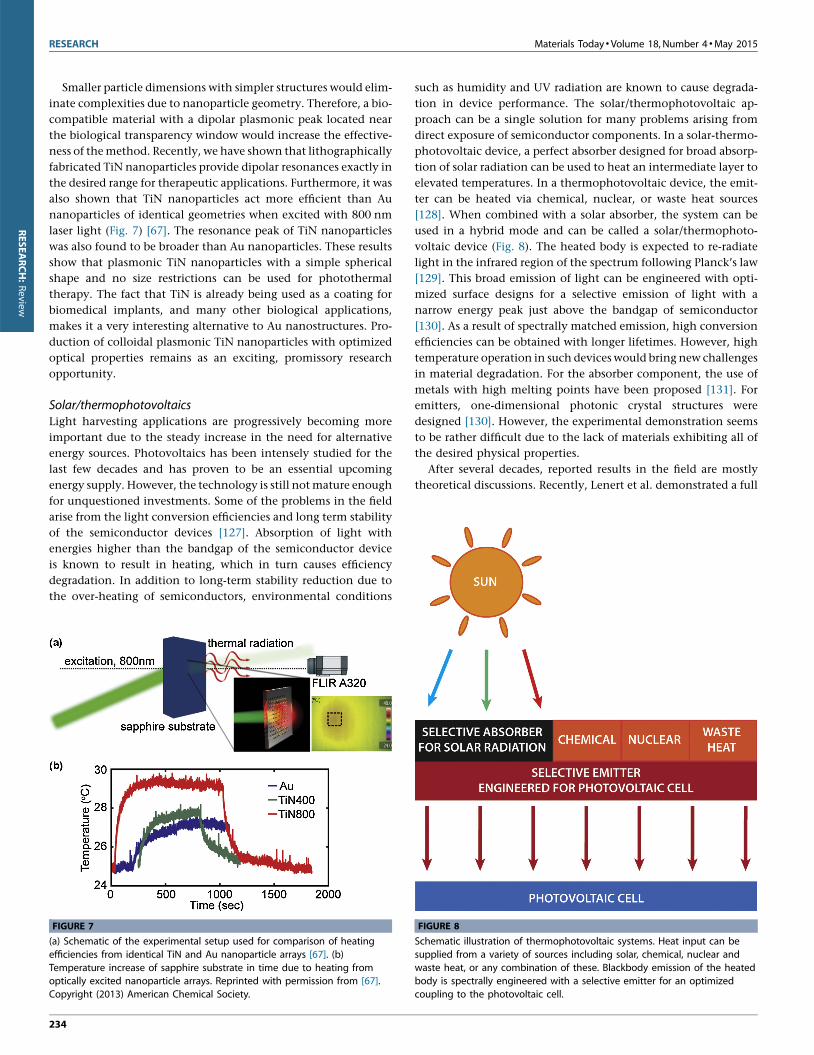
After several decades, reported results in the field are mostly
theoretical discussions. Recently, Lenert et al. demonstrated a full
FIGURE 8
Schematic illustration of thermophotovoltaic systems. Heat input can besupplied from a variety of sources including solar, chemical, nuclear and
waste heat, or any combination of these. Blackbody emission of the heated
body is spectrally engineered with a selective emitter for an optimized
coupling to the photovoltaic cell.

Materials Today � Volume 18, Number 4 �May 2015 RESEARCH
RESEARCH:Review
solar-thermophotovoltaic device with a record efficiency of 3.2%
[132]. In this pioneering work, the main limiting factors were the
spectral selectivity of the absorber and the relatively low opera-
tional temperatures due to material limitations. Plasmonic mate-
rials with refractory properties can solve both problems and
significantly push the experimental limits. We have shown that
broad absorption in the visible and near infrared regions can be
realized with a metamaterial design consisting of patterned rect-
angular rings which lead to an impedance match and reduced
reflection (Fig. 9(a)) [133]. In addition, owing to its adjustable
optical properties, TiN can be engineered to optimize the imped-
ance matching and can be used with a variety of perfect absorber
designs for efficient collection of energy from the sun. Recently,
Molesky et al. have proposed designs for selective emitters where
high melting point materials, including TiN, have been considered
[134]. TiN, with a melting point around 2900 8C, is again a very
promising plasmonic material. Fig. 9(b) shows the absorption
spectrum of an intact TiN absorber before and after annealing
at 800 8C. Indeed, the strength of TiN nanostructures has been
further tested and compared to Au when illuminated with a pulsed
laser for 5 seconds at 550 nm where both absorbers have high
absorbance. Scanning electron microscope images after test veri-
fies that TiN nanostructures can stand against high intensity
pulses where Au nanostructures fail (Fig. 9(c,d)) [133]. Durability
under high intensity laser illumination is inherently a desired
feature for nonlinear plasmonics [135].
Heat assisted magnetic recordingTip-based plasmonics is one broad application area where metallic
nanoparticles have been found useful. Apart from research appli-
cations such as near-field scanning optical microscopes (NSOM) or
other local field enhanced signal measurements, some commercial
applications like HAMR are also considered feasible. In magnetic
FIGURE 9
(a) Metamaterial perfect absorber design with high melting point materials.
(b) Measured absorbance of TiN perfect absorber before and afterannealing at 800 8C. (c) Au nanostructures illuminated with laser pulses
were highly damaged where (d) TiN nanostructures survived from laser
pulses under identical conditions. The scale bars in the figure are 400 nm.Reproduced with permission from [133]. Copyright 2014, John Wiley &
Sons, Inc.
recording technology, achieving higher data storage densities
requires the reduction of bit sizes, which brings new challenges
such as the loss of data in very small grains due to thermal
instabilities. Materials with higher magnetic anisotropy can be
used as a solution; however this would bring the need for higher
field strengths. A promising solution to the problem is to locally
heat the material to high temperatures and lower the coercivity for
a short amount of time during the writing process. The required
higher coercivity values that are needed for stable data storage can
be achieved by cooling the confined volume back to its initial
temperature [136]. Plasmonic nanoparticle-based tips have the
advantage of sub-wavelength focusing of electromagnetic energy
with high field strength and heating efficiencies in a confined
volume. Figure 10(a–c) illustrates an optically excited plasmonic
near field transducer (NFT) locally heating a bit-patterned layer,
the operation principles of HAMR, and the spatial distribution of
temperature and magnetic field on the medium. In 2009, Chall-
ener et al. integrated an NFT into a magnetic recording head and
demonstrated sub-wavelength recording on a high coercivity me-
dium at an operation wavelength of 830 nm [114]. However, long-
term stability of the system remains a problem due to tough
operation conditions. In their work, Challener et al. reported
operation temperatures above 350 8C. Thermal load on the NFT
can be reduced via alternative designs [137], however the long
term stability remains a challenge. For a long lifetime and reliabil-
ity, the nanostructured near-field transducer shall exhibit chemi-
cal stability and corrosion resistance [138,139], and the search for
alternative plasmonic materials become inevitable for HAMR
technology [140]. As we have been discussing through this review,
TiN is known to be corrosion resistant and durable at high tem-
peratures. It has been recently shown that optical properties of the
material slightly change with increasing temperatures up to 375 8C[141]. In addition, we have shown that the optical performance of
FIGURE 10
(a) Illustration of an optically excited plasmonic near field transducer (NFT)locally heating a bit-patterned medium. (b) A diagram of HAMR write
process. Reproduced with permission from [139]. Copyright 2008, IEEE. (c)
Magnetic field (dashed line) and temperature (solid line) distribution alongthe down track position for a HAMR design. Reproduced with permission
from [142]. Copyright 2012, The Optical Society.
235

RESEARCH Materials Today � Volume 18, Number 4 �May 2015
RESEARCH:Review
TiN nanoparticles is indeed comparable to identical Au nanopar-
ticles in the near infrared region where diode laser technology is
well established [143]. Therefore, near-field transducer designs
based on TiN nanostructures would bring the technology one step
closer to real life products.
OutlookResearch activities on the exciting field of plasmonics are steadily
getting more attention from researchers working across a broad
spectrum of science and technology. Accordingly, research
expenses are increasing continuously and the level of expectations
on practical results are getting higher. As the research area gets
more interdisciplinary, the integration of plasmonic components
to different technology standards becomes a necessity. A limited
pool of plasmonic materials would make it almost impossible to
satisfy fundamentally different requirements for each application
environment. Although Au and Ag have been very useful during
the initial research period in the ideal world of laboratory experi-
ments, alternative plasmonic materials are now essential require-
ments for day-to-day applications. TiN stands as a very promising
refractory plasmonic material for some critical applications that
require tough operating conditions. The high temperature dura-
bility, chemical stability, corrosion resistance and mechanical
strength of TiN are considered as great advantages over metals.
Furthermore, biological and CMOS compatibility of the material
makes it much easier to work with. Indeed, TiN has been already
employed in both biomedical and microelectronics technologies
and previous experience on material processing has been gained.
With the recent demonstrations of high optical efficiencies for
absorption based applications, TiN and other transition metal
nitrides become true plasmonic materials that can be employed
in technology products with minimal modification of production
chains.
AcknowledgementsThe authors acknowledge generous support from the following
grants: ARO grant 57981-PH (W911NF-11-1-0359), ONR-MURI
grant N00014-10-1-0942, NSF grant DMR-1120923. We are
thankful to Dr. Gururaj Naik, Dr. Alex Kildishev, Dr. Wei Li, Justus
C. Ndukaife, Nathaniel Kinsey, Clayton Devault for useful
discussions and help in preparation of this manuscript.
References
[1] M.A. Noginov, et al. Nature 460 (2009) 1110–1112.
[2] Z. Fang, et al. Nano Lett. 12 (2012) 3808–3813.
[3] V. Ortalan, A.H. Zewail, J. Am. Chem. Soc. 133 (2011) 10732–10735.
[4] J.R. Adleman, et al. Nano Lett. 9 (2009) 4417–4423.
[5] O. Neumann, et al. ACS Nano 7 (2012) 42–49.
[6] C. Loo, et al. Technol. Cancer Res. Treat. 3 (2004) 33–40.
[7] J.A. Scholl, A.L. Koh, J.A. Dionne, Nature 483 (2012) 421–427.
[8] N. Liu, et al. Nat. Mater. 10 (2011) 631–636.
[9] W.L. Barnes, A. Dereux, T.W. Ebbesen, Nature 424 (2003) 824–830.
[10] J.A. Schuller, et al. Nat. Mater. 9 (2010) 193–204.
[11] A. Belardini, et al. Phys. Rev. Lett. 107 (2011) 257401.
[12] S. Lal, S. Link, N.J. Halas, Nat. Photon. 1 (2007) 641–648.
[13] H.A. Atwater, Sci. Am. 296 (2007) 56–62.
[14] R. Zia, et al. Mater. Today 9 (2006) 20–27.
[15] D. Pile (Interviewer), J. Krenn (Interviewee), Nat. Photon. 6 (2012) 714–715.
[16] M. Faraday, Philos. Trans. R. Soc. Lond. 147 (1857) 145–181.
[17] J.M. Romo-Herrera, R.A. Alvarez-Puebla, L.M. Liz-Marzan, Nanoscale 3 (2011)
1304–1315.
236
[18] X. Ye, et al. ACS Nano 6 (2012) 2804–2817.
[19] P.R. West, et al. Laser Photon. Rev. 4 (2010) 795–808.
[20] G.V. Naik, V.M. Shalaev, A. Boltasseva, Adv. Mater. 25 (2013) 3264–3294.
[21] A.M. Smith, M.C. Mancini, S. Nie, Nat. Nanotechnol. 4 (2009) 710–711.
[22] L.R. Hirsch, et al. Proc. Natl. Acad. Sci. U. S. A. 100 (2003) 13549–13554.
[23] L.R. Hirsch, et al. Anal. Chem. 75 (2003) 2377–2381.
[24] G. Baffou, R. Quidant, C. Girard, Appl. Phys. Lett. 94 (2009) 153109.
[25] C.L. Nehl, H. Liao, J.H. Hafner, Nano Lett. 6 (2006) 683–688.
[26] A. Boltasseva, H.A. Atwater, Science 331 (2011) 290–291.
[27] J.-S.G. Bouillard, et al. Nano Lett. 12 (2012) 1561–1565.
[28] M.D. McMahon, et al. Appl. Phys. B 80 (2005) 915–921.
[29] W. Cao, H.E. Elsayed-Ali, Mater. Lett. 63 (2009) 2263–2266.
[30] A. Desireddy, et al. Nature 501 (2013) 399–402.
[31] G.H. Chan, et al. Nano Lett. 7 (2007) 1947–1952.
[32] G.H. Chan, et al. J. Phys. Chem. C 112 (2008) 13958–13963.
[33] M.G. Blaber, et al. Physica B 394 (2007) 184–187.
[34] M.G. Blaber, M.D. Arnold, M.J. Ford, J. Phys. Chem. C 113 (2009) 3041–3045.
[35] C. Radloff, N.J. Halas, Appl. Phys. Lett. 79 (2001) 674–676.
[36] A. Tittl, et al. Nano Lett. 13 (2013) 1816–1821.
[37] B. Gholipour, et al. Adv. Mater. 25 (2013) 3050–3054.
[38] N.K. Emani, et al. Nano Lett. 12 (2012) 5202–5206.
[39] C.-Y. Liu, et al. Opt. Express 19 (2011) 17092–17098.
[40] D.-K. Lim, et al. Nano Lett. 13 (2013) 4075–4079.
[41] I. Freestone, et al. Gold Bull. 40 (2007) 270–277.
[42] M.G. Blaber, M.D. Arnold, M.J. Ford, J. Phys.: Condens. Matter 21 (2009) 144211.
[43] D.A. Bobb, et al. Appl. Phys. Lett. 95 (2009) 151102–151103.
[44] M.G. Blaber, et al. Nano Lett. 12 (2012) 5275–5280.
[45] N. Strohfeldt, A. Tittl, H. Giessen, Opt. Mater. Exp. 3 (2013) 194–204.
[46] J. Wang, S. Liu, A. Nahata, Opt. Express 20 (2012) 12119–12126.
[47] Y. Sun, et al. J. Am. Chem. Soc. 126 (2004) 9399–9406.
[48] P.C. Wu, et al. Small 7 (2011) 751–756.
[49] J.M. Luther, et al. Nat. Mater. 10 (2011) 361–366.
[50] M. Kanehara, et al. J. Am. Chem. Soc. 131 (2009) 17736–17737.
[51] G. Garcia, et al. Nano Lett. 11 (2011) 4415–4420.
[52] R. Buonsanti, et al. Nano Lett. 11 (2011) 4706–4710.
[53] D.-K. Ko, J.J. Urban, C.B. Murray, Nano Lett. 10 (2010) 1842–1847.
[54] J. Kim, et al. IEEE J. Select. Top. Quant. Electron. 19 (2013) 4601907.
[55] U. Guler, A. Boltasseva, V.M. Shalaev, Science 344 (2014) 263–264.
[56] L. Roux, et al. Solar Energy Mater. 7 (1982) 299–312.
[57] D. Steinmuller-Nethl, et al. Thin Solid Films 237 (1994) 277–281.
[58] M. Wittmer, J. Vac. Sci. Technol. A: Vacuum Surf. Films 3 (1985) 1797–1803.
[59] A.P. Hibbins, J.R. Sambles, C.R. Lawrence, J. Mod. Opt. 45 (1998) 2051–2062.
[60] N.C. Chen, et al. J. Appl. Phys. 109 (2011) 043104.
[61] G.V. Naik, et al. Proc. Natl. Acad. Sci. U. S. A. 111 (2014) 7546–7551.
[62] N. Kinsey, et al. Opt. Express 22 (2014) 12238–12247.
[63] M. Quinten, Appl. Phys. B 73 (2001) 317–326.
[64] A. Reinholdt, et al. Eur. Phys. J. D: At. Mol. Opt. Plasma Phys. 31 (2004) 69–76.
[65] M. Cortie, J. Giddings, A. Dowd, Nanotechnology 21 (2010) 115201.
[66] U. Guler, et al. Appl. Phys. B 107 (2012) 285–291.
[67] U. Guler, et al. Nano Lett. 13 (2013) 6078–6083.
[68] H.O. Pierson, Handbook of Refractory Carbides & Nitrides: Properties, Charac-
teristics, Processing and Apps, William Andrew, Incorporated, 1996.
[69] G.K. Hyde, et al. Biomed. Mater. 4 (2009) 025001.
[70] T.E. Tang, et al. IEEE Trans. Electron Dev. 34 (1987) 682–688.
[71] N.T. Wakelyn, U.S.N. Aeronautics, S. Administration, Titanium Nitride: An
Oxidizable Coating for the High-Temperature Protection of Graphite, National
Aeronautics and Space Administration, 1961.
[72] S. Zhang, W. Zhu, J. Mater. Process. Technol. 39 (1993) 165–177.
[73] V. Lavrenko, V. Shvets, G. Makarenko, Powder Metall. Met. Ceram. 40 (2001)
630–636.
[74] A.J. Perry, J. Schoenes, Vacuum 36 (1986) 149–155.
[75] H. Wakabayashi, et al. IEEE Trans. Electron Dev. 48 (2001) 2363–2369.
[76] H.G. Tompkins, R. Gregory, B. Boeck, Surf. Interface Anal. 17 (1991) 22–24.
[77] H. Garcia, H. Krishna, R. Kalyanaraman, Appl. Phys. Lett. 89 (2006) 141109.
[78] F. Wang, Y.R. Shen, Phys. Rev. Lett. 97 (2006) 206806.
[79] V.M. Shalaev, AIP Conf. Proc. 560 (2001) 237–258.
[80] M.G. Blaber, M.D. Arnold, M.J. Ford, J. Phys.: Condens. Matter 22 (2010) 143201.
[81] H. Hovel, et al. Phys. Rev. B 48 (1993) 18178–18188.
[82] C. Bohren, D. Huffman, Absorption and Scattering of Light by Small Particles,
Wiley Science Paperback Series, Wiley-VCH, 1998.
[83] G. Mie, Ann. Phys. 330 (1908) 377–445.
[84] J. Sinzig, M. Quinten, Appl. Phys. A 58 (1994) 157–162.
[85] P.A. Bobbert, J. Vlieger, Physica A 137 (1986) 209–242.

Materials Today � Volume 18, Number 4 �May 2015 RESEARCH
RESEARCH:Review
[86] J.M. Gerardy, M. Ausloos, Phys. Rev. B 25 (1982) 4204–4229.
[87] M. Quinten, Optical Properties of Nanoparticle Systems: Mie and Beyond, Wiley,
2010.
[88] B.J. Messinger, et al. Phys. Rev. B 24 (1981) 649–657.
[89] L. Hultman, Vacuum 57 (2000) 1–30.
[90] P. Patsalas, S. Logothetidis, J. Appl. Phys. 90 (2001) 4725–4734.
[91] G.V. Naik, J. Kim, A. Boltasseva, Opt. Mater. Exp. 1 (2011) 1090–1099.
[92] G.V. Naik, et al. Opt. Mater. Exp. 2 (2012) 478–489.
[93] X. Yang, et al. J. Am. Ceram. Soc. 86 (2003) 206–208.
[94] J. Li, et al. J. Am. Ceram. Soc. 84 (2001) 3045–3047.
[95] J.P. Dekker, et al. J. Mater. Chem. 4 (1994) 689–694.
[96] J. Hu, et al. J. Am. Ceram. Soc. 83 (2000) 430–432.
[97] C. Giordano, et al. Chem. Mater. 21 (2009) 5136–5144.
[98] M. Ohwada, et al. Sci. Rep. 3 (2013).
[99] A. Frolich, et al. Adv. Mater. 25 (2013) 3588–3592.
[100] C. Unger, et al. Opt. Express 20 (2012) 24864–24872.
[101] S. Barcikowski, F. Mafune, J. Phys. Chem. C 115 (2011) 4985.
[102] N. Takada, T. Sasaki, K. Sasaki, Appl. Phys. A 93 (2008) 833–836.
[103] A. Calka, Appl. Phys. Lett. 59 (1991) 1568–1569.
[104] M. Kociak, J. Garcıa de Abajo, MRS Bull. 37 (2012) 39–46.
[105] E.J.R. Vesseur, et al. MRS Bull. 37 (2012) 752–760.
[106] B. Goris, et al. Nano Lett. 13 (2013) 4236–4241.
[107] H. Zheng, et al. Science 324 (2009) 1309–1312.
[108] M.J. Vasile, A.B. Emerson, F.A. Baiocchi, J. Vac. Sci. Technol. A: Vacuum Surf.
Films 8 (1990) 99–105.
[109] D. Jaeger, J. Patscheider, J. Electron Spectrosc. Relat. Phenom. 185 (2012) 523–534.
[110] N.C. Saha, H.G. Tompkins, J. Appl. Phys. 72 (1992) 3072–3079.
[111] D. Jaeger, J. Patscheider, Surf. Sci. Spectra 20 (2013) 1–8.
[112] J. Leiro, E. Minni, E. Suoninen, J. Phys. F: Met. Phys. 13 (1983) 215.
[113] S. Fan, Nat. Nano 9 (2014) 92–93.
[114] W. Challener, et al. Nat. Photon. 3 (2009) 220–224.
[115] D. Kraemer, et al. Nat. Mater. 10 (2011) 532–538.
[116] S. Linic, P. Christopher, D.B. Ingram, Nat. Mater. 10 (2011) 911–921.
[117] X. Zhou, et al. J. Mater. Chem. 22 (2012) 21337–21354.
[118] C. Clavero, Nat. Photon. 8 (2014) 95–103.
[119] D.A. Boyd, et al. Nano Lett. 6 (2006) 2592–2597.
[120] A.O. Govorov, H.H. Richardson, Nano Today 2 (2007) 30–38.
[121] C. Ayala-Orozco, et al. ACS Nano 8 (2014) 6372–6381.
[122] Y. Gao, et al. Small (2014).
[123] P. Huang, et al. Angew. Chem. Int. ed. 52 (2013) 13958–13964.
[124] A.M. Goodman, et al. ACS Nano 8 (2014) 3222–3231.
[125] Z. Li, et al. Mol. Pharm. 7 (2009) 94–104.
[126] S. Dasgupta, T. Auth, G. Gompper, Nano Lett. 14 (2014) 687–693.
[127] A. Polman, H.A. Atwater, Nat. Mater. 11 (2012) 174–177.
[128] T. Bauer, Thermophotovoltaics: Basic Principles and Critical Aspects of System
Design, Springer-Verlag, Berlin, Germany, 2011.
[129] M. Planck, The Theory of Heat Radiation, Springer-Verlag GmbH, 1906.
[130] E. Rephaeli, S. Fan, Opt. Express 17 (2009) 15145–15159.
[131] C. Wu, et al. J. Opt. 14 (2012) 024005.
[132] A. Lenert, et al. Nat. Nano 9 (2014) 126–130.
[133] W. Li, et al. Adv. Mater. (2014), http://dx.doi.org/10.1002/adma.201401874.
[134] S. Molesky, C.J. Dewalt, Z. Jacob, Opt. Express 21 (2013) A96–A110.
[135] M. Kauranen, A.V. Zayats, Nat. Photon. 6 (2012) 737–748.
[136] R.E. Rottmayer, et al. IEEE Trans. Magnet. 42 (2006) 2417–2421.
[137] S. Xiong, et al. J. Appl. Phys. 115 (2014), 17B702-717B702-703.
[138] N.C. Lindquist, et al. Laser Photon. Rev. 7 (2013) 453–477.
[139] M.H. Kryder, et al. Proc. IEEE 96 (2008) 1810–1835.
[140] N. Zhou, et al. Nanophotonics 3 (2014) 141–155.
[141] S. Tripura Sundari, et al. J. Appl. Phys. 115 (2014) 033516.
[142] T. Matsumoto, et al. Opt. Express 20 (2012) 18946–18954.
[143] U. Guler, et al. Farad. Discuss. (2014), http://dx.doi.org/10.1039/C4FD00208C.
237