Voltage linearity measurements using a binary Josephson system
Upload
independentCategory
view
2download
0
IL NUOVO CIMENTO VOL. 16 D, N. 12 Dicembre 1994
High-Tc Josephson Junctions for Electronic Applications (*).
S. PAGANO(1), S. BARBANERA(2), V. BOFFA(3), S. MATARAZZO(1), F. MURTAS(2) C. ROMEO(2), F. GATTA(3), U. GAMBARDELLA(4) and G. FILATRELLA(5)
(1) Isti tuto di Cibernetica del CNR - 1-80072 Arco Felice, Italia (2) Isti tuto di Elettronica dello Stato Solido del CNR - 1-00156 Roma, I taly (3) E N E A CRE Frascati - 1-00044 Frascati, I taly (4) INFN, L N F - 1-00044 Frascati, I taly (5) Dipartimento di Fisica dell'Universitd di Salerno - 1-84081 Baronissi (SA), I taly
(ricevuto il 17 Novembre 1994)
Summary. - - The current status of the electronic applications of high-T c Josephson junctions is briefly reviewed. Recent results obtained by the authors on devices employing step-edge junctions are reported. In particular the design of a microwave oscillator based on a parallel array of junctions is discussed and preliminary experimental results are presented.
PACS 74.50 - Proximity effects, tunneling phenomena, and Josephson effects. PACS 01.30.Cc - Conference proceedings.
1. - I n t r o d u c t i o n .
The possibility of fabricating reproducible and reliable high-Tr Josephson junctions is a key step toward the realization of superconducting devices of practical interest. Until now the development of a good junction fabrication technology has been difficult due to the peculiarities of the ceramic superconductors (small coherence length, surface defects, chemical unstability, anisotropic structure and properties, etc.). To overcome these difficulties, various techniques have been developed leading to a number of different junction configurations. Among these the best results have been obtained so far exploiting the intrinsic properties of this new class of superconductors, namely the grain boundary junctions, leading to two types of structures: the Bicrystal Grain Boundary (BGBJ) and Step Edge (SEJ) Junction. However, from the point of view of applications, these junctions suffer from a number of limitations as a low level of reproducibility (SEJ) and difficulty for large-scale integration (BGBJ). Other promising structures, based
(*) Paper presented at the ,,VII Congresso SATT,, Torino, 4-7 October 1994.
2095

2096 S. PAGANO, S. BARBANERA, V. BOFFA, ETC.
on epitaxially grown artificial barriers, while showing promising performances, can be considered still at a development stage [1].
In the following some considerations on the feasibility of high-Te Josephson- junctions applications in superconducting electronics will be made, our junction fabrication technology will de described, and experimental results on SQUID interferometers will be reported. Finally, a design for the microwave oscillator will be presented, together with results of numerical simulations and of preliminary experimental measurements.
2. - E l e c t r o n i c a p p l i c a t i o n s .
It is interesting to compare, for various applications of superconducting electronics, the performances of high-Tc junctions relatively to their low-To counterparts (see table I) [2].
When considering small-scale applications of superconductivity various issues have to be examined: the type of devices involved, the cryogenic requirements, the junction characteristic needed, the circuit complexity, etc. Moreover, a distinction must be made between applications where Josephson junctions offer unique performances, unattainable by other non-superconducting devices, and those where only performance improvements over existing techniques are provided. In the former case (e.g., for high-sensitivity biomagnetic measurements, voltage standard, etc.) the level of the performances obtainable usually compensates for the intrinsic technical difficulties and cost considerations. In the latter case the existence of evolving competitive technologies should always be born in mind when considering the balance between cost and benefit. A good example of this situation is the field of digital applications: until the last decade superconducting digital circuits, although suffering from poor reliability and reproducibility, were much faster than any semiconducting device. Since then superconducting digital circuits quality and reliability have constantly improved, but semiconductors have also dramatically improved in speed. As a consequence, the gap between these two competing technologies is now considerably reduced.
Among the junction requirements which are relevant for the possibility of realizing high-To-based devices are: the good shape of the I -V characteristics, the possibility for large-scale integration, the good value of IeRn and low intrinsic noise.
When the complexity of the superconducting circuit involved is not too high, and the requirements on the junction properties are not too stringent, high-Te-based devices are already competitive and have a realistic potential for marketing. This is the case for high-T~ SQUID magnetometers that have reached both a good degree of reliability and of performances, even competitive with those of the traditional low-Tc SQUIDs (when considering the complete device including the cryogenic part, the geometrical specifications, etc.).
Lately microwave superconducting devices have attracted considerable interest, mostly because of the possible application in telecommunication and space-born systems (see, e.g., the HTSSE I and II projects). One interesting principle for the realization of active superconducting microwave devices is the magnetic-flux flow in Josephson structures. A number of devices based on such principle have been proposed [3]. Among those we will focus on a microwave oscillator based on flux-flow

HIGH-T c JOSEPHSON JUNCTION FOR ELECTRONIC APPLICATIONS 2097
TABLE I. - List of applications of superconductive electronics [2]. For each application the type of structure involved~ the main requirements, and the degree of competitivity of high-Tr devices are reported.
Applications Device Requirements High-Tc competitivity
Magneto-encefalography Precision measurements
SQUID Very low noise Low Large Ir Low operating temperature Non-hysteretic I-V
Magneto-cardiography Biomagnetic measurements Geophysics Non-destructive evaluation
SQUID Low noise High Portability Non-hysteretic I-V
Voltage standard JJ arrays Junction reproducibility Low Large-scale integration Hysteretic I-V
Microwave amplifiers JJ arrays Junction reproducibility Average Medium-scale integration
S-I-S mixers JJ Large IcR n Low Low operating temperature Hysteretic I-V
Analog signal processing J J, SQUID Junction uniformity Low Large-scale integration
Digital circuits (latching) J J, SQUID Junction uniformity Low Large-scale integration Large IcRn Hysteretic I-V
Digital circuits (RSFQ logic) J J, SQUID Junction uniformity Low but Large-scale integration improving Large IcRn Non-hysteretic I-V
in a parallel array of high-To Josephson junctions, discussing in some detail its operation.
3. - High-Tc SQUIDs: fabrication and characterization.
Among the various junction fabrication technologies we have chosen that of Step Edge Junctions (SEJ) because it allows, in principle, a large-scale integration, and is therefore more suitable than others for complex devices development. The junctions are made by c-axis-oriented YBCO films deposited by laser ablation on MgO and SrTi03 substrates. The steps are made by Ar ion-milling on Nb-masked substrates. Subsequently, after the removal of the Nb layer, an YBCO film is deposited and

2098 S. PAGANO, S. BARBANERA, V. BOFFA, ETC.
120
f)
e) 80
0 0.05 0.10 0.15 0.20 magnetic field (G)
Fig. 1. - Experimental voltage modulation of a 2-junction YBCO interferometer, for various values of the bias current (a =-850y~A, b = - 8 7 0 ~ k , c=-880y2~, d = - 8 9 0 ~ k , e = - 9 0 0 ~ , f = - 9 3 0 y . A ) and at T=60K.
patterned by Ar ion-milling using a photoresist mask. YBCO film thickness of 1000/~ and step highs of 2000 A are typically obtained, while the step angle is about 70 ~ With this technique a number of junctions, alone and enclosed in superconducting loops, have been realized, with an average yield of about 50% and critical current density Jc ~ 104 A/cm2 at 77 K. As an example of the results that are typically achieved, in fig. 1 the flux-voltage modulation of a 2-junction interferometer (junctions width 2 ~m, loop area 250 ?m 2 , T = 60 K) is shown for various bias current values[4]. As for the majority of the high-To Josephson junctions the I-V characteristic is not hysteretical and does not show gap structures, thus indicating that a parallel quasi-particle conduction mechanism makes the junctions overdamped. This intrinsic feature prevents the use of such junctions for some of the applications in table I, like voltage standard, S-I-S mixers, latching logic, etc., while is not in principle a problem for others, like SQUID, RSFQ logic, etc. However a large value of IcRn is always required for all the applications.
4. - A paral le l SQUID array for m i c r o w a v e g e n e r a t i o n .
A parallel array of Josephson junctions can sustain, under appropriate circumstances, the propagation of magnetic flux quanta. This feature is at the heart of a number of new devices like vortex flow transitor (VFT), single-flux-quanta (SFQ) transmission lines, flux-flow amplifier (FFA), microwave oscillators, etc. [3, 5]. It consists of a number of Josephson junctions connected in parallel and having common electrodes. Each junction is connected to two adjacent junctions by a

HIGH-T c JOSEPHSON JUNCTION FOR ELECTRONIC APPLICATIONS 2099
Fig. 2. - Microphotograph of a 10-junctions array made with YBCO step-edge junctions. The horizontal line is the step of the substrate. The loop size is (20 x 10) t~m 2 and the link width is 3t~m.
superconducting loop. A bias current can be supplied to all the junctions in the ar ray through the electrodes, while a magnetic field can be applied locally by a control line or uniformly by a coil surrounding the whole device. In fig. 2 it is possible to see a microphotograph of a 10-junctions YBCO array made with the technique previously described (SEJ). The horizontal line is the step in the substrate, and the control line is the structure on the left.
We have modelled such device using the RSJ model for the Josephson junctions and considering only the nearest-neighbours magnetic coupling [6]. The resulting equations for the superconducting phase 9 of each junction is a discrete version of the well-known perturbed sine-Gordon equation:
1 (la) - -:- (gn-1
27~ + 9n+l - 29n) + ~n "}- ~ n "}- sing~ = ~" + -=- (V, - 9~n-1) ,
n = 2 . . . . . N - l ,
1 27r (15) - ~ (92 - 91) + ~1 -~- ~ 1 "~- s in91 -- Y -[- y (71 -~- ~u),
1 ( 2rr (lc) - ~ 9 N - I -- 9N) + ~N -[- ~ N + s ingN = Y ; (~N -[- ~u),
where fl = 2r:LIc/~O is the usual SQUID screening parameter, L the loop inductance, Ic the junction critical current, r the flux quantum, and a = (oJjRC) -1 is the normalized shunt conductance. C is the junction capacitance, R the intrinsic parallel resistance and o~i the plasma frequency. ), is the normalized bias current of the array, Vn (n = 1, ..., N) the normalized magnetic field due to the control line (which is a
2100 S. PAGANO, S. BARBANERA, V. BOFFA, ETC.
I o
2
1
0 0
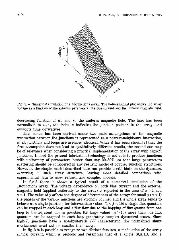
Fig. 3. - Numerical simulation of a 10-junctions array. The 3-dimensional plot shows the array voltage as a function of the external parameters: the bias current and the uniform magnetic field.
decreasing function of n), and ~u the uniform magnetic field. The time has been normalized to o~j -1 , the index n indicates the junction position in the array, and overdots time derivatives.
This model has been derived under two main assumptions: a) the magnetic interaction between the junctions is represented as a nearest-neighbours interaction, b) all junctions and loops are assumed identical. While it has been shown [7] that the first assumption does not lead to qualitatively different results, the second one may be of relevance when considering a practical implementation of the array with high-Te junctions. Indeed the present fabrication technology is not able to produce junctions with uniformity of parameters better than say 30-50%, so that large parameters scattering should be considered in any realistic model of coupled junction structures. However, the simple model described here can provide useful hints on the dynamics occurring in such array structure, leaving more detailed comparison with experimental data to more refined, and complex, models.
In fig. 3 there is shown a typical result of a numerical simulation of the 10-junctions array. The voltage dependence on both bias current and the external magnetic field (applied uniformly to the array) is reported in the case of ~ = 1 and /~ -- 1. The value of/~ affects the degree of discreteness of the array: for small/~ (~ < 1) the phases of the various junctions are strongly coupled and the whole array tends to behave as a single junction; for intermediate values (1 < fl < 10) a single flux quantum can be trapped in each loop and a flux flow due to the hopping of flux quanta from one loop to the adjacent one is possible; for large values (fl > 10) more than one flux quantum can be trapped in each loop generating complex dynamical states. Since high-Te junctions have a non-hysteretic I -V characteristic, the normalized shunt conductance must not be smaller than unity.
In fig. 3 it is possible to recognize two distinct features, a modulation of the array critical current, which is periodic and resembles that of a single SQUID, and a
HIGH-T c JOSEPHSON JUNCTION FOR ELECTRONIC APPLICATIONS 2101
modulation of the shape of the I i V curve, which is due to the flux-flow dynamics. Indeed, if a bias point is chosen in one of such structures, the array is in a regime in which flux quanta are continuously injected from one edge, and are ejected at the opposite one. If a load is attached to this edge it will sense a train of voltage pulses with frequency in the microwave range. The obtained values of frequency, power and linewidth depend on the actual parameters of the system and on the uniformity of the junctions. A detailed study is required in order to find the optimal configuration, also in consideration of the specific destination of the device.
5. - Pre l iminary exper imental results.
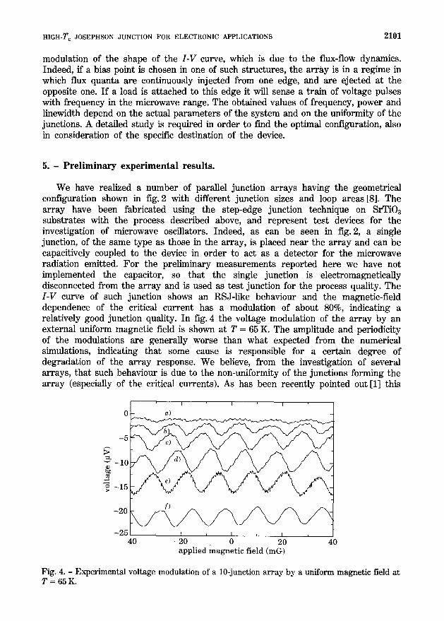
We have realized a number of parallel junction arrays having the geometrical configuration shown in fig. 2 with different junction sizes and loop areas [8]. The array have been fabricated using the step-edge junction technique on SrTi08 substrates with the process described above, and represent test devices for the investigation of microwave oscillators. Indeed, as can be seen in fig. 2, a single junction, of the same type as those in the array, is placed near the array and can be capacitively coupled to the device in order to act as a detector for the microwave radiation emitted. For the preliminary measurements reported here we have not implemented the capacitor, so that the single junction is electromagnetically disconnected from the array and is used as test junction for the process quality. The I -V curve of such junction shows an RSJ-like behaviour and the magnetic-field dependence of the critical current has a modulation of about 80%, indicating a relatively good junction quality. In fig. 4 the voltage modulation of the array by an external uniform magnetic field is shown at T = 65 K. The amplitude and periodicity of the modulations are generally worse than what expected from the numerical simulations, indicating that some cause is responsible for a certain degree of degradation of the array response. We believe, from the investigation of several arrays, that such behaviour is due to the non-uniformity of the junctions forming the array (especially of the critical currents). As has been recently pointed out [1] this
-5
~ -10 b~
- 1 5
-20 �84
-25 -41
I I I
- a)
" ~)
J I t I , I i
-20 0 20 40 applied magnetic field (raG)
Fig. 4. - Experimental voltage modulation of a 10-junction array by a uniform magnetic field at T = 65K.

2102 s. PAGANO, S. BARBANERA, V. BOFFA, ETC.
problem could be intrinsic to this junctions type (SEJ), thus indicating that other more reliable structures, like bicrystal grain boundary junctions or artificial barrier junctions, need to be employed.
6 . - C o n c l u s i o n s .
The status of electronic applications of high-Tr Josephson junctions has been briefly reviewed, indicating areas where these devices are competitive with the low-Tc counterparts and have a real market opportunity. We have reported our recent results on single SQUID interferometers and parallel SQUID arrays. The results on SQUID indicate that an average good level of performances can be obtained using the fabrication technology of step-edge junctions. On the other hand, our investigation of more complex structures as parallel array, while showing promising features for applications as microwave oscillators, vortex-flow transitor, etc., still do not show good experimental performances due to uniformity and reproducibility problems related to this type of junction.
$ $ $
We gratefully acknowledge the financial support of the Progetto Finalizzato ,,Superconductive and Cryogenic Technologies~ of the Consiglio Nazionale delle Ricerche of taly.
REFERENCES
[1] J. Z. SUN, L. S. YU-JAHNES, V. FOGLIETTI, R. H. KOCH and W. J. GALLAGHER: in Proceedings of Applied Superconductivity Conference, Boston, 199~, to appear in IEEE Trans. Supercond.; C. L. PETTIETE-HALL, J. A. LUINE, J. MURDUCK, J. F. BURCH, R. Hu, M. SERGANT and D. ST. JOHN: in Proceedings of Applied Superconductivity Conference, Boston, 199~, to appear in IEEE Trans. Supercond.
[2] A. BARONE and S. PAGANO: J. Supercond., 7, 375 (1994). [3] J. S. MARTENS, V. M. HIETALA, T. A. PLUT, D. S. GINLEY, G. A. VAWTER, C. P. TIGGERS,
M. P. SIEGEL, J. N. PHILLIPS and S. Y. Hou: IEEE Trans. Sup., 3, 2295 (1993). [4] S. MATARAZZO, S. BARBANERA, V. BOFFA, R. BRUZZESE, F. CICIULLA, U. GAMBARDELLA,
F. MURTAS, S. PAGANO, M. PENNA and C. ROMEO: J. Supercond., 6, 391 (1993). [5] K. K. LIKHAREV and V. K. SEMENOV: IEEE Trans. Supercond., 1, 13 (1991). [6] G. FILATRELLA, S. MATARAZZO and S. PAGANO: in Future Directions of Nonlinear Dynamics
in Physical and Biological Systems, edited by P. L. CHRISTIANSEN, C. EILBECK and R. D. PARMENTIER (Plenum Press, New York, N.Y., 1993), p. 347.
[7] J. n. PHILLIPS, H. S. J. VAN DER ZANT, J. WHITE and T. P. ORLANDO: Phys. Rev. B, 47, 5219 (1993); D. REINEL, W. DIETRICH, T. WOLF and A. MAJHOFER: Phys. Rev. B, 49, 9118 (1994).
[8] C. ROMEO, S. BARBANERA, V. BOFFA, G. FILATRELLA, U. GAMBARDELLA, F. GATTA, S. MATARAZZO, F. MURTAS and S. PAGANO: in Proceedings of Applied Superconductivity Conference, Boston, 199~, to appear in IEEE Trans. Supercond.
Copyright © 2022 FDOKUMEN