DC and RF Characterization of NiSi Schottky Barrier ...
166
Mitglied der Helmholtz-Gemeinschaft DC and RF Characterization of NiSi Schottky Barrier MOSFETs with Dopant Segregation Christoph Johannes Urban
-
Upload
khangminh22 -
Category
Documents
-
view
0 -
download
0
Transcript of DC and RF Characterization of NiSi Schottky Barrier ...
Info
rmat
ion
12 Mitg
lied
der
Hel
mho
ltz-G
emei
nsch
aft
DC and RF Characterization of NiSi Schottky Barrier MOSFETs with Dopant Segregation
Christoph Johannes Urban
Chr
isto
ph Jo
hann
es U
rban
DC
and
RF
Cha
ract
eriz
atio
n of
Nis
i SB-
MO
SFET
s
Information / InformationBand / Volume 12ISBN 978-3-89336-644-6
DC and RF Characterization
of NiSi Schottky Barrier MOSFETs
with Dopant Segregation
Von der Fakultat fur Mathematik, Informatik und Naturwissenschaften
der RWTH Aachen University zur Erlangung des akademischen Grades
eines Doktors der Naturwissenschaften genehmigte Dissertation
vorgelegt von
Diplom-Physiker (Univ.) Christoph Johannes Urban
aus Paderborn
Berichter: Universitatsprofessor Dr. S. Mantl
Universitatsprofessor Dr. M. Morgenstern
Tag der mundlichen Prufung: 27. April 2010
Diese Dissertation ist auf den Internetseiten der Hochschulbibliothek online verfugbar.
Forschungszentrum Jülich GmbHInstitute of Bio- and Nanosystems (IBN)Semiconductor Nanoelectronics (IBN-1)
DC and RF Characterization of NiSi Schottky Barrier MOSFETs with Dopant Segregation
Christoph Johannes Urban
Schriften des Forschungszentrums JülichReihe Information / Information Band / Volume 12
ISSN 1866-1777 ISBN 978-3-89336-644-6
Bibliographic information published by the Deutsche Nationalbibliothek.The Deutsche Nationalbibliothek lists this publication in the Deutsche Nationalbibliografie; detailed bibliographic data are available in the Internet at http://dnb.d-nb.de.
Publisher and Forschungszentrum Jülich GmbHDistributor: Zentralbibliothek 52425 Jülich Phone +49 (0) 24 61 61-53 68 · Fax +49 (0) 24 61 61-61 03 e-mail: [email protected] Internet: http://www.fz-juelich.de/zb Cover Design: Grafische Medien, Forschungszentrum Jülich GmbH
Printer: Grafische Medien, Forschungszentrum Jülich GmbH
Copyright: Forschungszentrum Jülich 2010
Schriften des Forschungszentrums JülichReihe Information / Information Band / Volume 12
D 82 (Diss., RWTH Aachen University, 2010)
ISSN 1866-1777ISBN 978-3-89336-644-6
The complete volume ist freely available on the Internet on the Jülicher Open Access Server (JUWEL) at http://www.fz-juelich.de/zb/juwel
Neither this book nor any part of it may be reproduced or transmitted in any form or by any means, electronic or mechanical, including photocopying, microfilming, and recording, or by any information storage and retrieval system, without permission in writing from the publisher.
Kurzfassung
Die fortschreitende Skalierung der Silizium-basierten Mikroelektronik, welche die Basis
der heutigen Informationsgesellschaft bildet, bedarf neuer Konzepte fur die Source-
Drain (S/D) Kontakte der Metall-Oxid-Halbleiter Feldeffekttransistoren (MOSFET).
Dabei ist insbesondere eine Verbesserung der Ladungstragerinjektion wichtig, da der
zunehmende Einfluss der parasitaren Widerstande die Leistungsfahigkeit von hochgra-
dig skalierten Bauelementen stark begrenzt. Daruber hinaus werden immer abruptere
Ubergange zwischen Kontakt und Kanal fur Bauelemente auf der Nanometerskala er-
forderlich. In diesem Zusammenhang sind Schottky-Barrieren (SB) MOSFETs mit
metallischen S/D Kontakten sehr vielversprechend, da sich mit ihnen niedrige ex-
trinsische Widerstande und atomar abrupte Kontakt-Kanal-Ubergange an den Metall-
Silizium Grenzflachen realisieren lassen. Ein großer Nachteil ist jedoch, dass die Leis-
tungsfahigkeit dieser Bauelemente der von konventionellen MOSFETs aufgrund der
relativ hohen Schottky-Barriere unterlegen ist. Kurzlich erregte die sogenannte Dotier-
stoffsegregation großes Interesse, da die bei der Silizidierung entstandene hochdotierte
Schicht an der Silizid-Silizium Grenzflache die Tunnel-Wahrscheinlichkeit von Ladungs-
tragern durch Schottky-Kontakte stark erhoht.
Die vorliegende Arbeit untersucht experimentell die Integration von NiSi mit Dotier-
stoffsegregation fur den Einsatz in SB-MOSFETs auf dunnem Silizium-auf-Isolator
(SOI). Ziel der detaillierten Gleichstrom (DC) und Hochfrequenz (RF) Charakter-
isierung ist der Erhalt eines besseren Einblickes in die Physik dieser Bauelemente.
Die Modellierung von NiSi/p-Si Schottky-Kontakten mit Hilfe eines numerischen Mo-
delles, welches die Thermische-Emissions-Theorie mit der Barrierenverkleinerung durch
Spiegelladungen und quantenmechanischem Tunneln kombiniert, vertieft das Verstand-
nis der Ladungstragerinjektion von Schottky-Kontakten. Schottky-Dioden mit Dotier-
stoffsegregation von Bor, Arsen und Antimon, die durch die Silizidierung herbeigefuhrt
wurde, zeigen abhangig von der Implantationsdosis effektive Schottky-Barrieren-Hohen
um 0.1 eV. Unterhalb dieses Wertes sind SB-MOSFETs in der Lage die Leistungsfahig-
keit von konventionellen Bauelementen zu ubertreffen.
Erfolgreich hergestellte Lang- und Kurzkanal p- und n-typ SB-MOSFETs mit und
ohne Dotierstoffsegregation werden durch DC-Messungen charakterisiert. Transistoren
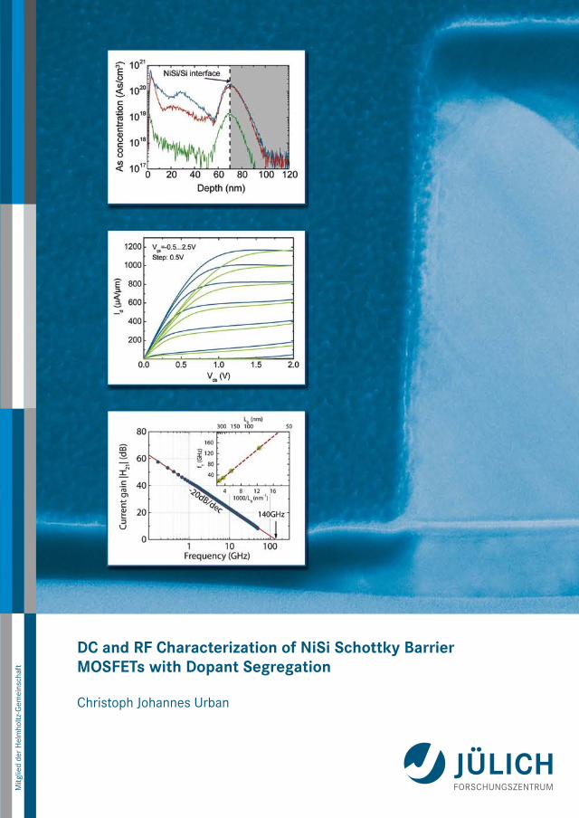
mit 80 nm Kanallange zeigen dabei hohe An-Strome von 427μA/μm fur p-typ und
1150μA/μm fur n-typ MOSFETs, welche vergleichbar zu anderen hochmodernen SB-
MOSFETs sind.
Erstmalig werden durch Streuparameter-Messungen die extrinsischen und intrinsischen
Eigenschaften von n- und p-typ SB-MOSFETs mit NiSi extrahiert. Die Hochfrequenz-
eigenschaften der Bauelemente zeigen ein perfekt lineares Skalierungsverhalten und
hohe Grenzfrequenzen von 140 GHz fur n-typ und 63 GHz fur p-typ SB-MOSFETs
mit einer Kanallange von 80 nm. Die Optimierung des reproduzierbaren Herstel-
lungsprozesses verbesserte die Source/Drain Widerstande um 30% auf 508 Ωμm fur
Bauelemente, die auf 20 nm dunnem SOI hergestellt wurden. Obwohl die DC Leistungs-
fahigkeit der SB-MOSFETs durch eine hohe Schottky-Barriere stark veschlechtert wird,
hat diese nur einen geringen Einfluß auf die Grenzfrequenz. Dies kann durch das glei-
che Verhalten der Transkonduktanz und der Gate-Kapazitat bei veranderten Implanta-
tionsdosen und damit Schottky-Barrier-Hohen erklart werden. Ein Vergleich der Grenz-
frequenzen mit hochmodernen MOSFETs verdeutlicht die ausgezeichnete Leistungs-
fahigkeit der hergestellten Bauelemente und deutet eine eindrucksvolle Verbesserung
dieser fur eine weitere Miniaturisierung an. Parameter, welche die Hochfrequenzeigen-
schaften limitieren und die Ursache fur eine Variabilitat der Leistungsfahigkeit der
SB-MOSFETs werden eingehend diskutiert.
Zusammenfassend zeigt diese Arbeit ein hohes Potential der NiSi S/D SB-MOSFETs
mit Dotierstoffsegregation fur eine Nutzung in der hochgradig skalierten Mikroelek-
tronik auf.
Abstract
The continuous downscaling of the Si-based microelectronics, which is the fundament
of today’s information technology, requires novel concepts for the source/drain (S/D)
architecture of metal-oxide-semiconductor field-effect transistors (MOSFETs). The
improvement of the carrier injection is of prime importance because of the increas-
ing impact of parasitic resistances which strongly limit the performance of ultimately
scaled transistors. Moreover, steeper junctions at the contact/channel interfaces be-
come more and more crucial for nanoscale devices. In this context, Schottky-barrier
(SB) MOSFETs with metallic S/D are promising performance boosters since they offer
low extrinsic resistances and atomically abrupt junctions formed at the metal/silicon
interface. However, a drawback of these devices is their performance which is inferior to
conventional MOSFETs due to the relatively high Schottky barrier. Recently, dopant
segregation has attracted much interest since the highly doped layer formed at the
silicide/silicon interface during silicidation strongly improves the tunneling probability
of carriers through Schottky contacts.
The present thesis studies the integration of NiSi with dopant segregation in SB-
MOSFETs on thin-body silicon-on-insulator experimentally. The objective of the de-
tailed direct-current (DC) and radio-frequency (RF) characterization is to gain a better
insight into the physics of these devices.
The modeling of NiSi/p-Si Schottky contacts using a numerical model which com-
bines the thermionic emission theory with image-force induced barrier lowering and
quantum-mechanical tunneling provides a solid understanding of the carrier injection
of Schottky contacts. The characterization of Schottky diodes with silicidation induced
dopant segregation using boron, arsenic and antimony reveals effective Schottky bar-
rier heights in the 0.1 eV regime depending on the implantation dose. Below this value
SB-MOSFETs are capable of outperforming conventional MOSFETs.
Successfully fabricated long- and short-channel p- and n-type SB-MOSFETs with and
without dopant segregation are characterized performing direct-current (DC) measure-
ments. Transistors with 80 nm channel length reveal on-currents as high as 427μA/μm
for p-type and 1150μA/μm for n-type devices, respectively, which compete well with
state-of-the-art SB-MOSFETs.
For the first time, the extrinsic and intrinsic device parameters of short-channel n- and
p-type NiSi SB-MOSFETs are extracted using scattering parameter measurements.
The radio-frequency (RF) investigation of the devices reveals a perfectly linear scaling
and high cut-off frequencies of 140 GHz for n-type and 63 GHz for p-type SB-MOSFETs
with a gate length of 80 nm. The optimization of the reproducible fabrication pro-
cess improves the S/D resistances by 30% and yields a value of 508 Ωμm for devices
fabricated on 20 nm thick silicon-on-insulator. Although, the DC performance of SB-
MOSFETs is strongly deteriorated by high Schottky barriers, it has only a small impact
on the cut-off frequency. This can be explained by the similar behavior of the transcon-
ductance and the total gate capacitance when the implantation dose and therefore the
Schottky barrier height is changed. The benchmarking of the obtained cut-off frequen-
cies with state-of-the-art MOSFETs demonstrates the superior RF performance of the
fabricated devices and predicts an impressive performance increase for further down-
scaling. RF performance limiting parameters are identified and the origin of the RF
variability of SB-MOSFETs is discussed.
In summary, the results of this work demonstrate a high potential of NiSi S/D SB-
MOSFETs with dopant segregation for a use in ultimately scaled microelectronics.
Contents
1 Introduction 1
2 Basic Principles 5
2.1 The MOS Capacitor . . . . . . . . . . . . . . . . . . . . . . . . . . . . 5
2.2 Fundamentals of MOSFETs . . . . . . . . . . . . . . . . . . . . . . . . 7
2.3 Long-Channel MOSFET . . . . . . . . . . . . . . . . . . . . . . . . . . 9
2.4 Important DC-Parameters . . . . . . . . . . . . . . . . . . . . . . . . . 12
2.5 Short-Channel MOSFETs . . . . . . . . . . . . . . . . . . . . . . . . . 14
2.5.1 Scaling Rules . . . . . . . . . . . . . . . . . . . . . . . . . . . . 14
2.5.2 Short-Channel Effects . . . . . . . . . . . . . . . . . . . . . . . 15
2.6 SOI Substrates . . . . . . . . . . . . . . . . . . . . . . . . . . . . . . . 17
2.7 Parasitic Resistances and Capacitances . . . . . . . . . . . . . . . . . . 19
3 Nickel Silicide 21
3.1 Introduction . . . . . . . . . . . . . . . . . . . . . . . . . . . . . . . . . 21
3.2 Formation of NiSi . . . . . . . . . . . . . . . . . . . . . . . . . . . . . . 22
3.3 Dopant Segregation . . . . . . . . . . . . . . . . . . . . . . . . . . . . . 25
4 Schottky-Diodes 27
4.1 Ideal Metal-Semiconductor Contacts . . . . . . . . . . . . . . . . . . . 27
4.2 Current Transport in Schottky Contacts . . . . . . . . . . . . . . . . . 28
4.3 Thermionic Emission Theory . . . . . . . . . . . . . . . . . . . . . . . . 29
4.4 Real Metal-Semiconductor Contacts . . . . . . . . . . . . . . . . . . . . 30
4.5 Extraction of the Schottky Barrier Height . . . . . . . . . . . . . . . . 33
i
Contents
4.5.1 The Arrhenius Plot . . . . . . . . . . . . . . . . . . . . . . . . . 33
4.5.2 Thermionic Emission Theory combined with Tunneling . . . . . 35
4.5.3 Model Application and Validation . . . . . . . . . . . . . . . . . 37
4.6 Fabrication of SB-Diodes . . . . . . . . . . . . . . . . . . . . . . . . . . 39
4.7 Temperature-Dependent Measurements . . . . . . . . . . . . . . . . . . 40
4.8 NiSi/p-Si Contacts with B Segregation . . . . . . . . . . . . . . . . . . 41
4.9 NiSi/n-Si Contacts with As Segregation . . . . . . . . . . . . . . . . . . 43
4.10 NiSi/n-Si Contacts with Sb Segregation . . . . . . . . . . . . . . . . . . 45
4.11 Summary . . . . . . . . . . . . . . . . . . . . . . . . . . . . . . . . . . 46
5 Fabrication Process of SB-MOSFETs 49
5.1 Mask Design . . . . . . . . . . . . . . . . . . . . . . . . . . . . . . . . . 49
5.2 Layout of SB-MOSFETs . . . . . . . . . . . . . . . . . . . . . . . . . . 51
5.3 Fabrication Process . . . . . . . . . . . . . . . . . . . . . . . . . . . . . 52
6 DC-Characteristics of SB-MOSFETs 57
6.1 Gate Oxide . . . . . . . . . . . . . . . . . . . . . . . . . . . . . . . . . 57
6.2 Operation Principle of SB-MOSFETs . . . . . . . . . . . . . . . . . . . 59
6.3 Long-Channel MOSFETs . . . . . . . . . . . . . . . . . . . . . . . . . . 60
6.3.1 NiSi S/D SB-MOSFETs . . . . . . . . . . . . . . . . . . . . . . 61
6.3.2 p-Type SB-MOSFETs with Dopant Segregation . . . . . . . . . 63
6.3.3 n-Type SB-MOSFETs with Dopant Segregation . . . . . . . . . 66
6.3.4 S/D Resistances . . . . . . . . . . . . . . . . . . . . . . . . . . . 68
6.4 Short-Channel SB-MOSFETs . . . . . . . . . . . . . . . . . . . . . . . 70
6.5 Optimized Devices . . . . . . . . . . . . . . . . . . . . . . . . . . . . . 75
6.6 Strained SOI . . . . . . . . . . . . . . . . . . . . . . . . . . . . . . . . 77
6.7 Benchmarking . . . . . . . . . . . . . . . . . . . . . . . . . . . . . . . . 80
6.8 Summary . . . . . . . . . . . . . . . . . . . . . . . . . . . . . . . . . . 82
ii
Contents
7 RF-Characterization 83
7.1 Scattering-Parameters . . . . . . . . . . . . . . . . . . . . . . . . . . . 83
7.2 Small-Signal Model of the SOI MOSFET . . . . . . . . . . . . . . . . . 84
7.2.1 Useful Transistor Effect . . . . . . . . . . . . . . . . . . . . . . 85
7.2.2 Quasi-Static Model . . . . . . . . . . . . . . . . . . . . . . . . . 85
7.2.3 Nonquasi-Static Model . . . . . . . . . . . . . . . . . . . . . . . 86
7.2.4 Extrinsic Model and Access Elements . . . . . . . . . . . . . . . 87
7.3 Characterization Method . . . . . . . . . . . . . . . . . . . . . . . . . . 90
7.3.1 De-Embedding Procedure . . . . . . . . . . . . . . . . . . . . . 90
7.3.2 Extrinsic Series Resistances . . . . . . . . . . . . . . . . . . . . 91
7.3.3 Extraction of the Capacitances and Conductances . . . . . . . . 92
7.4 Measurement Procedure . . . . . . . . . . . . . . . . . . . . . . . . . . 93
7.5 Gate-Length Dependence . . . . . . . . . . . . . . . . . . . . . . . . . . 95
7.5.1 Extrinsic Series Resistances . . . . . . . . . . . . . . . . . . . . 95
7.5.2 Capacitances . . . . . . . . . . . . . . . . . . . . . . . . . . . . 96
7.5.3 Intrinsic Conductance . . . . . . . . . . . . . . . . . . . . . . . 100
7.5.4 Cut-Off Frequency and Maximum Oscillation Frequency . . . . 101
7.5.5 Experiment vs. Calculation . . . . . . . . . . . . . . . . . . . . 104
7.6 Gate-Width Dependence . . . . . . . . . . . . . . . . . . . . . . . . . . 105
7.7 SB-MOSFET with an Optimized Process Flow . . . . . . . . . . . . . . 107
7.7.1 Extrinsic Series Resistances . . . . . . . . . . . . . . . . . . . . 107
7.7.2 Dose-Dependence of the RF Performance . . . . . . . . . . . . . 108
7.7.3 Optimized 80 nm n-type SB-MOSFET . . . . . . . . . . . . . . 110
7.8 Comparison of state-of-the-art SB-MOSFETs . . . . . . . . . . . . . . 110
7.9 Limiting Parameters . . . . . . . . . . . . . . . . . . . . . . . . . . . . 112
7.10 Summary . . . . . . . . . . . . . . . . . . . . . . . . . . . . . . . . . . 113
8 Variability 115
9 Conclusion and Outlook 119
Bibliography 121
iii
Contents
A Abbreviations 139
B S-Parameter Relationships 141
C List of Publications 143
D Acknowledgement 147
E Curriculum Vitae 151
iv
Chapter 1
Introduction
The fundament of today’s information technology is the Si-based microelectronics
whose tremendous miniaturization has allowed the fabrication of increasingly power-
ful microprocessors and memory chips. The continuous downscaling of the integrated
circuits in microelectronics was predicted by Gordon E. Moore in 1965. His empirical
observation, the so-called Moore’s law, states that the number of transistors which can
be placed at low-costs on an integrated circuit is doubled every two years [1]. Du-
ring the past 40 years, the microelectronics industry has followed Moore’s law and the
transistor feature size was scaled from 10μm to approximately 30 nm, guided by the
International Technology Roadmap for Semiconductors (ITRS). The objective of the
ITRS which is adapted every second year is to ensure cost-effective advancements in
the performance of the integrated circuits and the products that employ such devices,
thereby continuing the health and success of the semiconductor industry [2].
While the performance increase has mainly relied on the scaling of the device dimen-
sions, physical and technological limits are reached as the complementary metal-oxide-
semiconductor (CMOS) technology is entering the decananometer regime. One of the
most important challenges for ultimately scaled metal-oxide-semiconductor field-effect
transistors (MOSFETs) is the improvement of the carrier injection because of the
increasing impact of the parasitic resistances on the transistor performance [3]. Op-
timized S/D architectures are of prime importance for enhancing the on-current of
MOSFETs which is required, for instance, for high radio-frequency (RF) performance.
Schottky barrier (SB) MOSFETs with metallic S/D electrodes are regarded as an at-
tractive alternative to conventional MOSFETs with highly doped S/D regions since
they offer superior scaling abilities due to low extrinsic resistances and atomically
abrupt junctions formed at the metal/silicon interface [4]. These benefits are com-
plemented by low formation temperatures of the typically used silicides and a CMOS
1
Chapter 1. Introduction
compatible process flow. Especially, for ultimately scaled, fully depleted ultra-thin
body (UTB) silicon-on-insulator (SOI) MOSFETs, metallic S/D junctions are promis-
ing performance boosters, as the electrical properties of these devices are strongly
limited by parasitic resistances.
The concept of SB-MOSFETs, was first proposed by Nishi in 1966 and patented in
1970 [5]. In 1968 Lepselter and Sze published the first paper on SB-MOSFETs using
PtSi S/D [6]. However, SB-MOSFETs exhibit an intrinsic performance inferior to con-
ventional devices due to the Schottky barrier formed at the metal/channel interfaces.
As a result, they suffer from low on-currents, a poor subthreshold swing and ambipolar
switching. Recently, simulations have demonstrated that SB-MOSFETs with Schot-
tky barrier heights (SBH) lower than 0.1 eV are capable of outperforming conventional
MOSFETs [7, 8]. Therefore, over the last few years intensive research on SB-MOSFETs
has been devoted to improve the carrier injection. As a result, three main concepts
have been investigated.
• The use of rare-earth silicides like ErSi [9, 10] or YbSi [11] for n-MOSFETs and
PtSi [11–13] for p-MOSFETs with the lowest known Schottky barrier heights for
electrons (0.27-0.36 eV) and holes (0.15-0.27 eV), respectively, has shown impres-
sive results.
• Fermi level depinning with an insulator placed between the metallic electrode
and the semiconductor is an alternative to reduce the Schottky barrier height
[14–16].
• Another very promising approach is the combination of silicides like PtSi or the
midgap material NiSi with dopant segregation. Different techniques with im-
plantation to silicide (ITS) followed by a drive-in anneal [17, 18], implantation
to metal (ITM) [17] and the silicidation induced dopant segregation [4, 19] have
been reported. In all cases dopants pile-up at the silicide/silicon interface during
dopant segregation and form a thin highly doped layer which causes a strong
band bending. As a consequence, the tunneling probability of carriers through
the effectively lowered Schottky barrier increases significantly. Recent theoreti-
cal investigations consider the Schottky barrier height modulation as a result of
dopant induced dipoles formed at the NiSi/Si interface [20–22].
Key benefits of dopant segregation using NiSi are easy formation, low costs, CMOS
compatibility and much lower Schottky barrier heigths if compared to the other pro-
posed methods. Therefore, the present thesis studies the use of NiSi in combination
2
with dopant segregation as silicide for SB-MOSFETs on thin-body SOI experimen-
tally. A detailed direct-current (DC) and radio-frequency (RF) characterization offers
physical insights into these devices.
• Chapter 2 Fundamentals and device concepts of MOSFETs are introduced,
including short-channel effects which deteriorate the performance of ultimately
scaled devices. Moreover, this chapter explains the key device parameters which
are used for device characterization and benchmarking.
• Chapter 3 Since NiSi is used for the fabrication of SB-MOSFETs, the formation
of nickel-silicides is discussed briefly and fundamentals of silicidation induced
dopant segregation are presented.
• Chapter 4 The physical modeling of NiSi/p-Si Schottky contacts using an
appropriate numerical transport model provides a solid understanding of the car-
rier injection of Schottky contacts. A quantitative analysis of Schottky diodes
with dopant segregation is performed by temperature-dependent I-V measure-
ments and the extraction of the effective Schottky barrier heights. This chapter
provides the fundamentals which are necessary to understand SB-MOSFET ope-
ration with and without dopant segregation.
• Chapter 5 The development of a mask layout and a reproducible process
technology facilitates the fabrication of long-channel as well as short-channel
SB-MOSFETs. The ground-signal-ground (GSG) layout of the two-finger SB-
MOSFETs in combination with dedicated test structures allows for RF charac-
terizations.
• Chapter 6 Successfully fabricated p- and n-type SB-MOSFETs with and with-
out dopant segregation are characterized using direct-current (DC) measure-
ments. Peculiarities of these SB-MOSFETs are discussed and key device pa-
rameters are extracted from the I-V charactersitics. Moreover, the 80 nm-short
channel devices are compared with state-of-the-art SB-MOSFETs.
• Chapter 7 After introducing the fundamentals of the scattering (S) parameter
theory and the small-signal equivalent circuit of MOSFETs, this chapter pro-
vides for the first time a detailed RF analysis of dopant-segregated p- and n-type
NiSi SB-MOSFETs. The S-parameter measurements facilitate the extraction of
the extrinsic and intrinsic device parameters as a function of the device dimen-
sions and implantation dose, i. e., the Schottky barrier height. The 80 nm-short
channel devices are compared with state-of-the-art MOSFETs and a trend of the
3
Chapter 1. Introduction
performance increase of the fabricated SB-MOSFETs is given. Finally, the most
important parameters which limit the RF performance are identified.
• Chapter 8 This chapter discusses the variability of the RF performance of
SB-MOSFETs and elaborates their origin.
4

Chapter 2
Basic Principles
This chapter gives an introduction to the most important fundamentals and device
concepts of metal-oxide-semiconductor field-effect transistors (MOSFETs). After con-
sidering the MOS capacitor which provides the knowledge for an understanding of
MOS-related devices, the basic principles of MOSFETs are introduced. Next to the
examination of long-channel devices, the specific characteristics of short-channel MOS-
FETs are presented and discussed. Finally, the advantages of silicon-on-insulator sub-
strates are presented and the crucial impact of parasitic resistances and capacitances
is discussed.
2.1 The MOS Capacitor
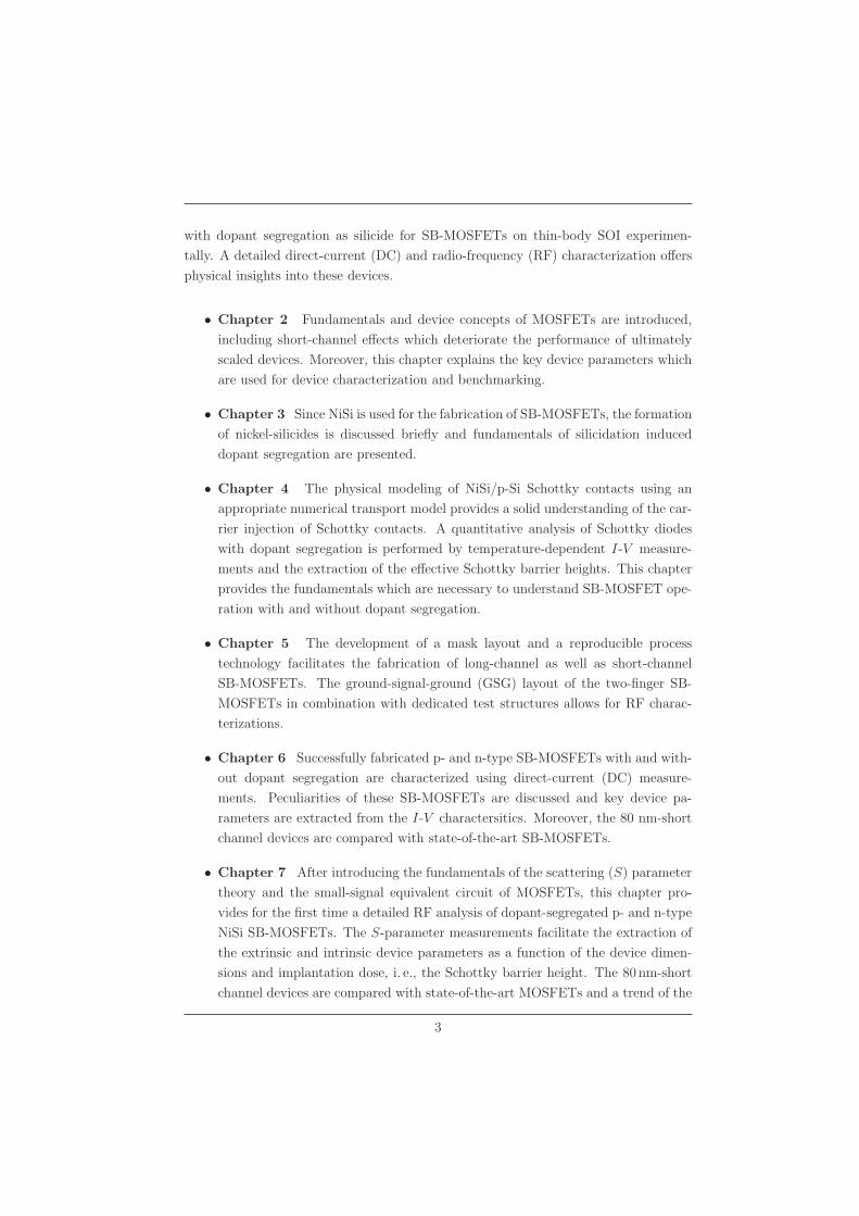
Fig. 2.1 shows a cross-section of an ideal MOS capacitor with its energy-band diagram
in the case of a p-type semiconductor at equilibrium (V = 0). Note, that the difference
between the metal work function Φm and the semiconductor work function is zero:
Vms = Φm −(
χSi +EG
2q+ Φbp
)= 0 (2.1)
χSi is the electron affinity of the semiconductor, EG the bandgap and Φbp the difference
between the intrinsic Fermi level Ei and the valence band edge EV . Under this condition
the conduction and valence bands are flat (flat-band condition) at equilibrium according
to the requirement of a common Fermi level throughout the structure.
5
Chapter 2. Basic Principles
Vgb
Metal
Oxide
Ohmic contact
Semiconductor EFm EFsEV
EC
Ei
Vacuum level
qΦm
qχSi
EG/2qΦbp
(a) (b)
Metal Oxide Semiconductor
Figure 2.1: (a) Illustration of the MOS capacitor. (b) Energy band diagram of
an ideal MOS capacitor built on a p-type semiconductor at equilibrium (V = 0).
q: elementary charge, Φm: metal workfunction, χSi: electron affinity for semicon-
ductor, EG: bandgap, EFm, EFs: Fermi level of the metal and the semiconductor,
EC : bottom edge of the conduction band, EV : top edge of the valence band, Ei:
intrinsic Fermi level.
When a MOS capacitor is biased with an external voltage a surface potential Φs arises
at the semiconductor-insulator interface and changes its charge distribution. In the
depletion approximation the voltage dependence of the surface potential can be written
as [23]:
Vgb = Vfb + Φs − QS
Cox
= Vfb + Φs +
√2εSiqNΦs
Cox
(2.2)
where Vfb is flat-band voltage, Cox the oxide capacitance, N the doping concentration
of the semiconductor and εSi the permittivity of the semiconductor. Depending on the
applied external voltage Vgb different cases of the surface potential Φs, illustrated in
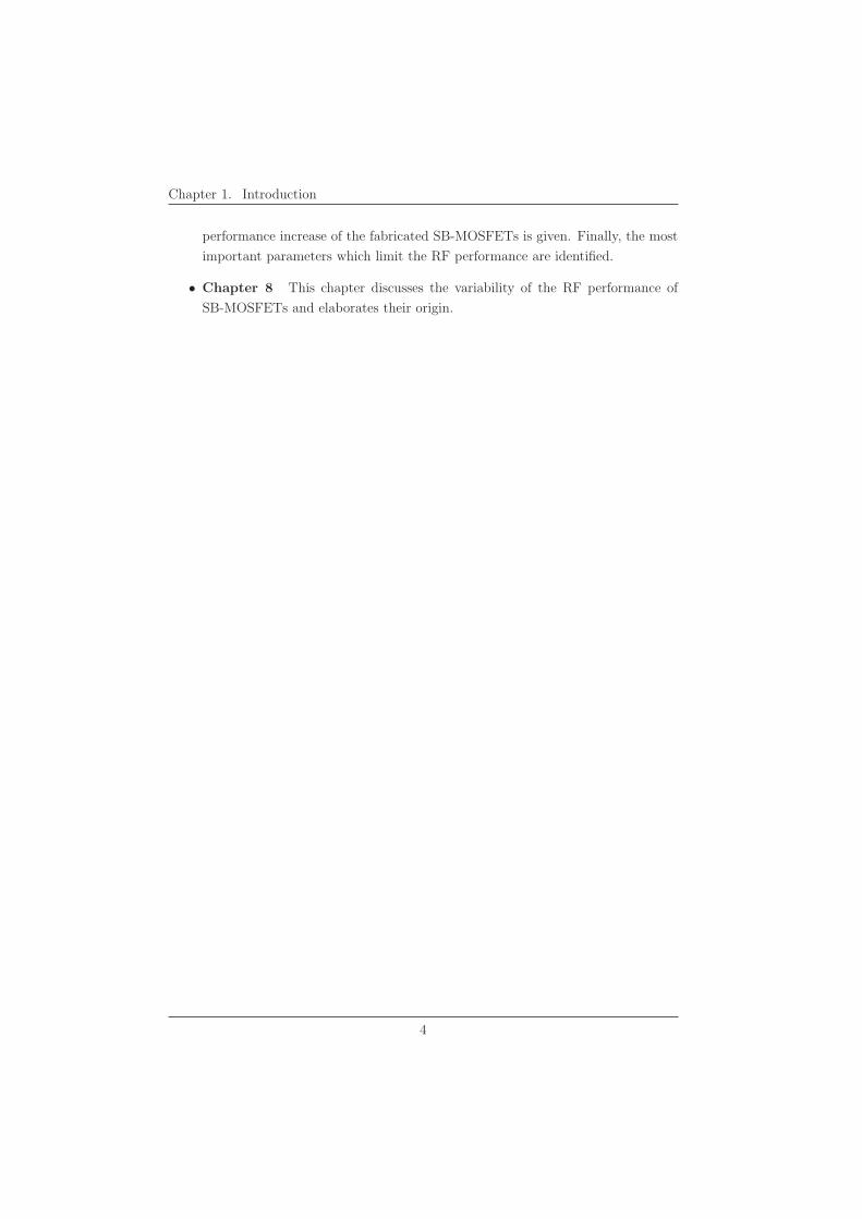
Fig. 2.2, can be distinguished [24]:
• Φs < 0 (accumulation): When Vgb is smaller than the flat-band voltage Vfb holes
accummulate at the oxide/semiconductor interface, which results in an upward
band bending.
• Φs = 0 (flat-band): The bands are flat and show no bending (Fig. 2.1(b)). The
applied voltage Vgb compensates possible differences of the workfunctions of the
metal and the semiconductor.
• Φbp > Φs > 0 (depletion): For Vgb > Vfb holes are depleted from the interface
leading to a lower hole concentraton than in the p-type bulk-Si which results in
a downward band bending.
6
2.2. Fundamentals of MOSFETs
• 2Φbp > Φs > Φbp (weak inversion): When Vgb becomes sufficiently positive to
attract a significant number of free electrons to the silicon/oxide interface, the
electron density will exceed the hole density at the interface.
• Φs > 2Φbp (strong inversion): With further increase of Vgb the Fermi level EFs
lies well above the intrinsic Fermi level Ei. The change of the surface potential
Φs with the gate voltage is more and more reduced because the inversion charge
screens the electric field generated by Vgb.
Figure 2.2: The MOS capacitor in (a) equilibrium, (b) accumulation, (c) onset
of inversion and (d) strong inversion.
2.2 Fundamentals of MOSFETs
The MOSFET is a three terminal structure which consists of a MOS capacitor with
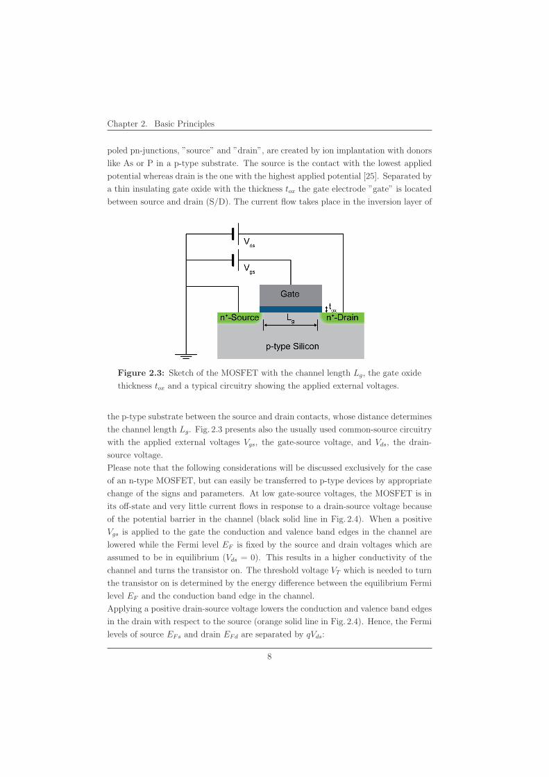
highly conducting contacts to the left and to the right of the inversion layer. Fig. 2.3
illustrates an n-type MOSFET fabricated on a p-type silicon substrate. The two reverse
7
Chapter 2. Basic Principles
poled pn-junctions, ”source” and ”drain”, are created by ion implantation with donors
like As or P in a p-type substrate. The source is the contact with the lowest applied
potential whereas drain is the one with the highest applied potential [25]. Separated by
a thin insulating gate oxide with the thickness tox the gate electrode ”gate” is located
between source and drain (S/D). The current flow takes place in the inversion layer of
Figure 2.3: Sketch of the MOSFET with the channel length Lg, the gate oxide
thickness tox and a typical circuitry showing the applied external voltages.
the p-type substrate between the source and drain contacts, whose distance determines
the channel length Lg. Fig. 2.3 presents also the usually used common-source circuitry
with the applied external voltages Vgs, the gate-source voltage, and Vds, the drain-
source voltage.
Please note that the following considerations will be discussed exclusively for the case
of an n-type MOSFET, but can easily be transferred to p-type devices by appropriate
change of the signs and parameters. At low gate-source voltages, the MOSFET is in
its off-state and very little current flows in response to a drain-source voltage because
of the potential barrier in the channel (black solid line in Fig. 2.4). When a positive
Vgs is applied to the gate the conduction and valence band edges in the channel are
lowered while the Fermi level EF is fixed by the source and drain voltages which are
assumed to be in equilibrium (Vds = 0). This results in a higher conductivity of the
channel and turns the transistor on. The threshold voltage VT which is needed to turn
the transistor on is determined by the energy difference between the equilibrium Fermi
level EF and the conduction band edge in the channel.
Applying a positive drain-source voltage lowers the conduction and valence band edges
in the drain with respect to the source (orange solid line in Fig. 2.4). Hence, the Fermi
levels of source EFs and drain EFd are separated by qVds:
8
2.3. Long-Channel MOSFET
EFs − EFd = qVds (2.3)
Consequently, the channel is in a non-equilibrium state. For a simple system with the
energy E, an expression for the steady-state current can be obtained [26]:
Id ∝ 2q
h
∫ ∞
−∞T (E)[fs(E) − fd(E)]dE (2.4)
where h is the Planck constant, T (E) the transmission probability and fs/fd the Fermi-
functions of source/drain. This simple equation illustrates basic facts of the transistor
operation. If fs(E) = fd(E) no current will flow. For energies significantly below EFs
and EFd, fs(E) = fd(E) = 1 and consequently no current flows, as well as for energies
well above EFs and EFd where fs(E) = fd(E) = 0. This means, that a drain current
Id will only flow for energies which lie within a few kBT of the potentials EFs and EFd.
Figure 2.4: Band diagram of an n-channel MOSFET. The black line represents
the off-state of the transistor (Vgs = 0, Vds = 0), passing into the on-state with
Vgs > 0, Vds > 0 (orange line).
2.3 Long-Channel MOSFET
In case of long-channel MOSFETs the channel length Lg is much longer than the
depletion zones of the pn-junctions at S/D. Therefore, these depletion zones can be
neglected. In the gradual-channel approximation, which is the base for the following
description of the basic MOSFET characteristics, the potential distribution can be
9
Chapter 2. Basic Principles
regarded as one-dimensional [27]. One key assumption of this approximation is that
the variation of the transverse electric field Ez perpendicular to the channel is much
larger than the corresponding variation of the longitudinal field Ex along the channel.
Therefore, the behavior of the MOSFET is mainly determined by the potential along
the z-direction. A second assumption which allows the derivation of analytical solutions
for the drain current is the charge sheet model in which the inversion layer is treated
as a charge sheet with zero thickness [28]. This gives the following equation for the
drain current:
Id =Wg
Lg
μeffCox
{(Vgs − Vfb − 2Φbp − Vds
2
)Vds
−2
3
√2ε0εSiqNA
Cox
[(Vds + 2Φbp)
3/2 − (2Φbp)3/2
]} (2.5)
Wg is the gate width, μeff the carrier mobility, ε0 the dielectric constant, εSi the
permittivity of the semiconductor and NA the acceptor impurity concentration. Equa-
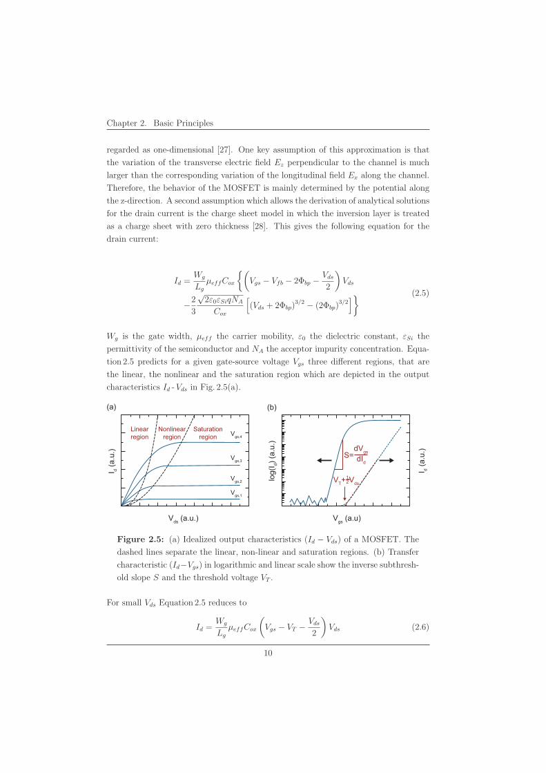
tion 2.5 predicts for a given gate-source voltage Vgs three different regions, that are
the linear, the nonlinear and the saturation region which are depicted in the output
characteristics Id -Vds in Fig. 2.5(a).
Vgs (a.u)
log(
I d) (a
.u.)
I d (a.
u.)
Vds (a.u.)
I d (a.
u.)
Saturationregion
Linearregion
Nonlinearregion
Vgs,1
Vgs,2
Vgs,3
Vgs,4
VT+ Vds
(a) (b)
dIdS=
dVgs
12
Figure 2.5: (a) Idealized output characteristics (Id − Vds) of a MOSFET. The
dashed lines separate the linear, non-linear and saturation regions. (b) Transfer
characteristic (Id−Vgs) in logarithmic and linear scale show the inverse subthresh-
old slope S and the threshold voltage VT .
For small Vds Equation 2.5 reduces to
Id =Wg
Lg
μeffCox
(Vgs − VT − Vds
2
)Vds (2.6)
10
2.3. Long-Channel MOSFET
with the threshold voltage VT , given by
VT = Vfb + 2Φbp +
√2εSiqNA (2Φbp)
Cox
(2.7)
Equation 2.6 indicates that, in the linear region, the MOSFET behaves like a resistor
with a sheet resistivity ρsh = 1/ [μeffCox (Vgs − VT )] which can be modulated by the
gate-source voltage Vgs. With increasing Vds the drain current passes the non-linear
region and saturates at Idsat which can be obtained by setting dId/dVds = 0:
Idsat =1
2n
Wg
Lg
μeffCox (Vgs − VT )2 (2.8)
n is the so-called body-factor, with n = 1+ Cc
Cox, which depends on the oxide capacitance
Cox and on the capacitance of the depletion layer Cc. In the following, the occurance of
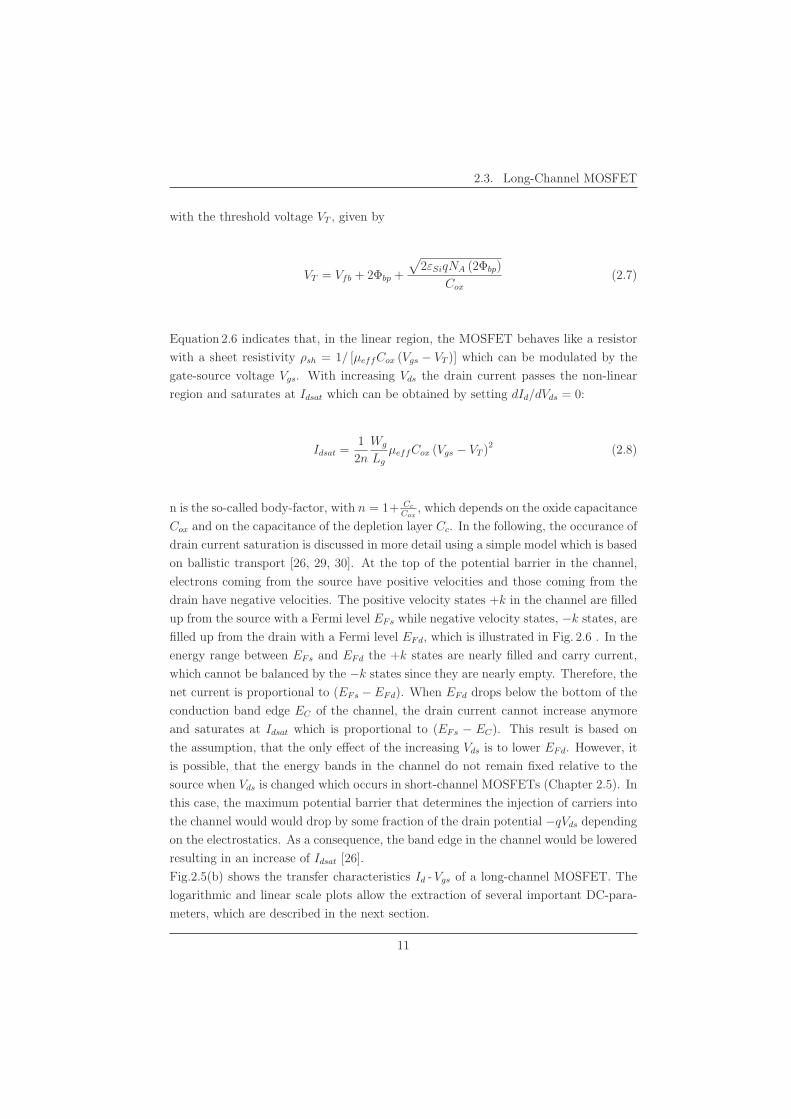
drain current saturation is discussed in more detail using a simple model which is based
on ballistic transport [26, 29, 30]. At the top of the potential barrier in the channel,
electrons coming from the source have positive velocities and those coming from the
drain have negative velocities. The positive velocity states +k in the channel are filled
up from the source with a Fermi level EFs while negative velocity states, −k states, are
filled up from the drain with a Fermi level EFd, which is illustrated in Fig. 2.6 . In the
energy range between EFs and EFd the +k states are nearly filled and carry current,
which cannot be balanced by the −k states since they are nearly empty. Therefore, the
net current is proportional to (EFs − EFd). When EFd drops below the bottom of the
conduction band edge EC of the channel, the drain current cannot increase anymore
and saturates at Idsat which is proportional to (EFs − EC). This result is based on
the assumption, that the only effect of the increasing Vds is to lower EFd. However, it
is possible, that the energy bands in the channel do not remain fixed relative to the
source when Vds is changed which occurs in short-channel MOSFETs (Chapter 2.5). In
this case, the maximum potential barrier that determines the injection of carriers into
the channel would would drop by some fraction of the drain potential −qVds depending
on the electrostatics. As a consequence, the band edge in the channel would be lowered
resulting in an increase of Idsat [26].
Fig.2.5(b) shows the transfer characteristics Id -Vgs of a long-channel MOSFET. The
logarithmic and linear scale plots allow the extraction of several important DC-para-
meters, which are described in the next section.
11
Chapter 2. Basic Principles
-k +k
E(k)
EC
EC-qVds
EFd=EFs-qVdsEFd
EFs EFs
EC
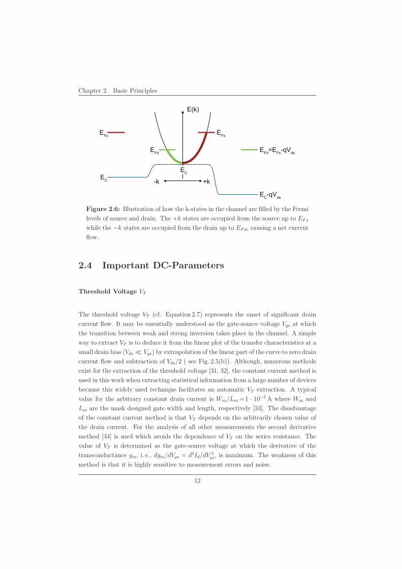
Figure 2.6: Illustration of how the k-states in the channel are filled by the Fermi
levels of source and drain. The +k states are occupied from the source up to EFs
while the −k states are occupied from the drain up to EFd, causing a net current
flow.
2.4 Important DC-Parameters
Threshold Voltage VT
The threshold voltage VT (cf. Equation 2.7) represents the onset of significant drain
current flow. It may be essentially understood as the gate-source voltage Vgs at which
the transition between weak and strong inversion takes place in the channel. A simple
way to extract VT is to deduce it from the linear plot of the transfer characteristics at a
small drain bias (Vds � Vgs) by extrapolation of the linear part of the curve to zero drain
current flow and subtraction of Vds/2 ( see Fig. 2.5(b)). Although, numerous methods
exist for the extraction of the threshold voltage [31, 32], the constant current method is
used in this work when extracting statistical information from a large number of devices
because this widely used technique facilitates an automatic VT extraction. A typical
value for the arbitrary constant drain current is Wm/Lm = 1 · 10−7 A where Wm and
Lm are the mask designed gate width and length, respectively [33]. The disadvantage
of the constant current method is that VT depends on the arbitrarily chosen value of
the drain current. For the analysis of all other measurements the second derivative
method [34] is used which avoids the dependence of VT on the series resistance. The
value of VT is determined as the gate-source voltage at which the derivative of the
transconductance gm, i. e., dgm/dVgs = d2Id/dV 2gs, is maximum. The weakness of this
method is that it is highly sensitive to measurement errors and noise.
12
2.4. Important DC-Parameters
Inverse Subthreshold Slope S
The inverse subthreshold slope S quantifies which gate-source voltage range is needed
to switch a MOSFET from the off-state to the on-state. It is defined as the gate-source
voltage needed to increase the drain current by one order of magnitude [24]:
S = ln (10)kBT
q
(1 +
CC
Cox
)(mV/dec) (2.9)
CC is the capacitance of the semiconductor space-charge region where the electrical
charges are composed of the inversion layer charge and ionized acceptor atoms form-
ing the depletion layer charge. The inverse subthreshold slope can be determined by
linear fitting of the logarithmic transfer characteristics, see Fig. 2.5(b). The theoretical
minimum of S is 60 mV/dec at room temperature for devices with thermal injection
of carriers. Recently, band-to-band tunneling transistors have attracted much interest
since they potentially offer the ability of having inverse subthreshold slopes less than
60 mV/dec due to field-effect controlled band-to-band tunneling [35–39].
Transconductance Gm
The transconductance Gm of a MOSFET is a measure of the gate control over drive
current modulation. It is given by the first derivative of Id with respect to Vgs:
Gm =dId
dVgs
∣∣∣∣Vds
(S) (2.10)
In general, Gm increases in inverse proportion to the gate length Lg. However, when
the gate length falls to the deep submicrometer level the increase drops off, because
the S/D resistance and velocity saturation of carriers limit Gm [40].
Gate Induced Drain Leakage
A large component of off-state leakage current is gate induced drain leakage (GIDL),
caused by band-to-band tunneling in the drain region underneath the gate stack. It
occurs when the gate-to-drain bias is sufficient that the energy-band bending close to
the Si/gate-dielectric interface is large enough that valence-band electrons can tunnel
into the conduction band. GIDL is an obstacle for gate-oxide thickness scaling be-
cause the voltage required to cause this band-to-band tunneling current decreases with
the gate oxide thickness. Especially for low-power circuit applications the off-state
leakage current plays an important role. Moreover, GIDL can pose a lower limit for
13
Chapter 2. Basic Principles
standby power in memory devices, but it becomes less significant for digital logic ap-
plications where the power-supply voltage is reduced to below 1.1 V, corresponding to
the energy band gap of silicon [41]. GIDL appears in the transfer characteristics as a
Vds-dependent off-state current which is indicated in Fig 2.7(b). A similar off-current
branch is observed for SB-MOSFETs due to an ambipolar switching behavior, which
is discussed in Chapter 6.2.
Mobility μeff
The mobility μeff is defined as the proportionality constant between the drift velocity
vx and the electric field strength Ex at low electric fields:
vx = μeff · Ex (2.11)
Carrier scattering with acoustic phonons and ionized impurities significantly affects the
mobility of nonpolar semiconductors such as Si and Ge. In principle, two methods for
the mobility extraction of MOSFETs are used. On the one hand, it is possible to use
the Id/√
gm-method which is a very simple method that is often used for the mobility
extraction of Pseudo-MOSFETs [42]. On the other hand, split capacitance-voltage
(C-V) measurements facilitate the extraction of μeff versus the effective field Ez which
is perpendicular to the transport direction [43, 44].
2.5 Short-Channel MOSFETs
When the channel length decreases the spatial extent of the depletion widths of S/D
become more and more comparable to the channel length. In this case, short-channel
effects (SCE) arise as a result of a two-dimensional potential distribution and high elec-
tric fields in the channel region. The one-dimensional gradual-channel approximation
(Ez >> Ex) is no longer valid and the potential distribution in the channel depends on
the transverse electric field Ez as well as on the longitudinal field Ex. In the following,
scaling rules are presented which ensure long-channel behavior of MOSFETs when the
gate length is scaled down. Since deviations from this behavior cannot be avoided
completely, the most crucial SCE are introduced.
2.5.1 Scaling Rules
Although, many scaling rules have been proposed [45, 46], the most-ideal rule to avoid
SCE is to scale down all device dimensions and voltages of a long-channel MOSFET
14
2.5. Short-Channel MOSFETs
in a way that the electric fields in the transistor are sustained [47]. This constant-field
scaling includes a shrinking of all device dimensions and potentials by a factor 1/κ and
an increase of the doping concentration by a factor κ, leading to a reduction of the
depletion width. However, further downscaling becomes more and more complicated
since the junction built-in voltage and the surface potential for the onset of weak
inversion do not scale. Therefore, the supply voltage cannot be scaled as it is required in
highly integrated circuits in order to reduce the power consumption. Moreover, physical
limitations have become a major problem. Gate leakage currents induced by tunneling
through the ultra-thin gate oxides [48] as well as increased S/D resistances Rs/d when
the junction depths are decreased have been huge challenges in the last few years.
With these limitations scaling rules have been proposed which allow the adjustment of
various device parameters independently as long as the transistor behavior is preserved
[49]. According to reference [49] the channel length Lg must be larger than Lmin in
order to achieve long-channel behavior
Lmin = 0.41A[tjtox (Ws + Wd)
2]1/3(2.12)
with the implantation depth tj, the gate-oxide thickness tox and the S/D depletion
widths Ws and Wd. In the case of planar SOI MOSFETs which are introduced in
Chapter 2.6 devices are free of short-channel effects if the effective gate length is larger
than five to ten times the natural length λ [46]:
λ =
√εSi
εox
tSitox (2.13)
where λ can be derived from Poisson’s equation. The natural length of a device basically
represents the length of the region of the channel that is controlled by the drain [50].
2.5.2 Short-Channel Effects
Though, the presented scaling rules should keep the long-channel behavior when devices
are scaled down, SCE cannot be totally prevented. They are a result of a loss of the
gate control as well as an increasing influence of the drain potential. In contrast
to the transfer and output characteristics of long-channel MOSFETs, discussed in
Chapter 2.3, short-channel devices show major differences in the electrical behavior.
For example, the drain current Id does not saturate at high Vds (Fig. 2.7(a)). The
threshold voltage shifts to lower values with increasing drain bias Vds (Fig. 2.7(b)) and
also with decreasing channel length Lg.
15
Chapter 2. Basic Principles
0 0.5 1.0 1.5 2.0
200
400
600
800
1000
1200
I d (μ
A/μ
m)
Vds (V)-2 -1 0 1 2
10-7
10-5
10-3
10-1
10+1
10+3
I d (μA
/μm
)
Vgs (V)
Vds=0.3...1.5VStep: 0.6V
Vgs=-0.5...2.5VStep: 0.5V
(a) (b)
DIBL
DIBLGIDL
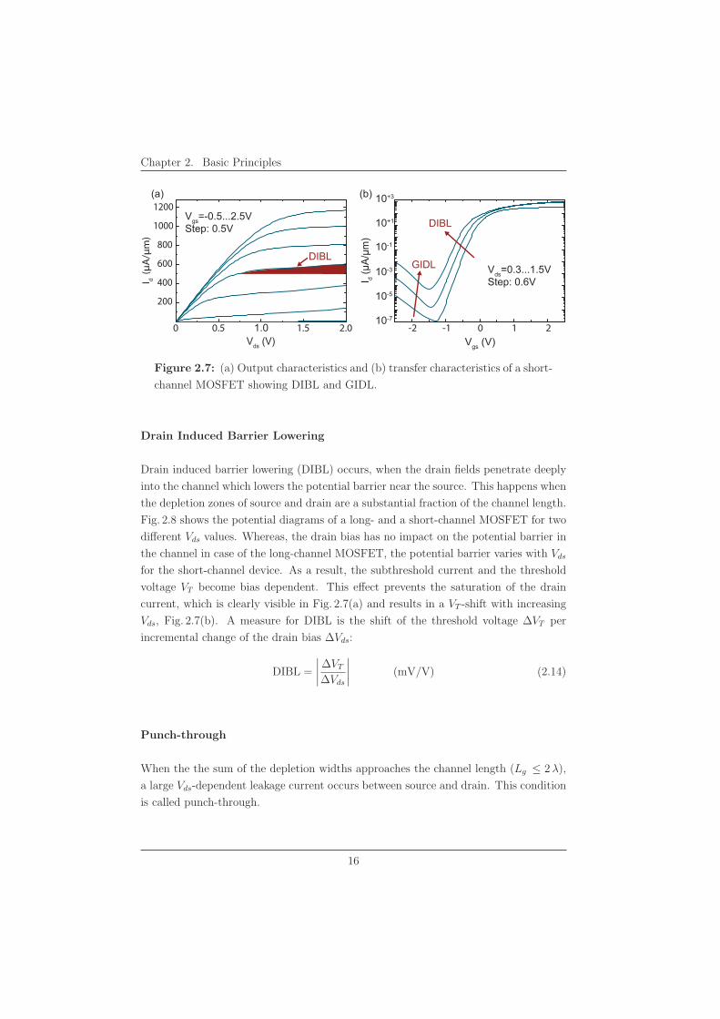
Figure 2.7: (a) Output characteristics and (b) transfer characteristics of a short-
channel MOSFET showing DIBL and GIDL.
Drain Induced Barrier Lowering
Drain induced barrier lowering (DIBL) occurs, when the drain fields penetrate deeply
into the channel which lowers the potential barrier near the source. This happens when
the depletion zones of source and drain are a substantial fraction of the channel length.
Fig. 2.8 shows the potential diagrams of a long- and a short-channel MOSFET for two
different Vds values. Whereas, the drain bias has no impact on the potential barrier in
the channel in case of the long-channel MOSFET, the potential barrier varies with Vds
for the short-channel device. As a result, the subthreshold current and the threshold
voltage VT become bias dependent. This effect prevents the saturation of the drain
current, which is clearly visible in Fig. 2.7(a) and results in a VT -shift with increasing
Vds, Fig. 2.7(b). A measure for DIBL is the shift of the threshold voltage ΔVT per
incremental change of the drain bias ΔVds:
DIBL =
∣∣∣∣ ΔVT
ΔVds
∣∣∣∣ (mV/V) (2.14)
Punch-through
When the the sum of the depletion widths approaches the channel length (Lg ≤ 2 λ),
a large Vds-dependent leakage current occurs between source and drain. This condition
is called punch-through.
16
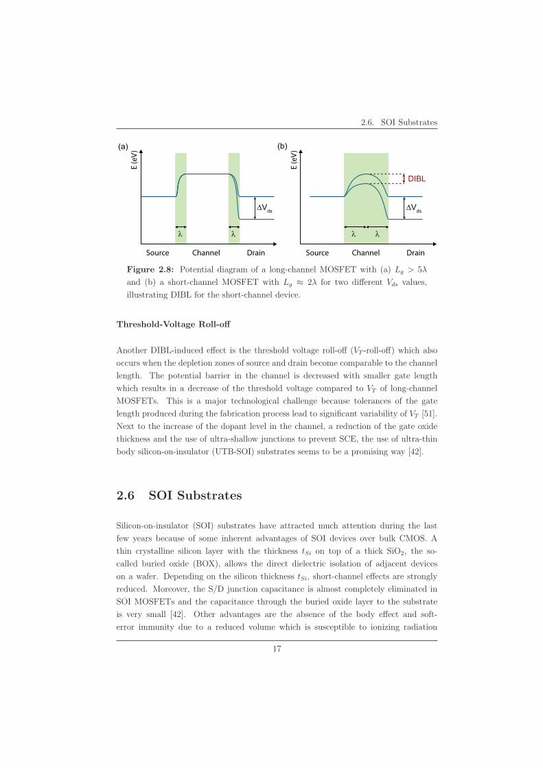
2.6. SOI Substrates
Source Channel Drain
E (e
V)
λ λ λ λ
Source Channel Drain
E (e
V)(a) (b)
DIBL
ΔVds ΔVds
Figure 2.8: Potential diagram of a long-channel MOSFET with (a) Lg > 5λ
and (b) a short-channel MOSFET with Lg ≈ 2λ for two different Vds values,
illustrating DIBL for the short-channel device.
Threshold-Voltage Roll-off
Another DIBL-induced effect is the threshold voltage roll-off (VT -roll-off) which also
occurs when the depletion zones of source and drain become comparable to the channel
length. The potential barrier in the channel is decreased with smaller gate length
which results in a decrease of the threshold voltage compared to VT of long-channel
MOSFETs. This is a major technological challenge because tolerances of the gate
length produced during the fabrication process lead to significant variability of VT [51].
Next to the increase of the dopant level in the channel, a reduction of the gate oxide
thickness and the use of ultra-shallow junctions to prevent SCE, the use of ultra-thin
body silicon-on-insulator (UTB-SOI) substrates seems to be a promising way [42].
2.6 SOI Substrates
Silicon-on-insulator (SOI) substrates have attracted much attention during the last
few years because of some inherent advantages of SOI devices over bulk CMOS. A
thin crystalline silicon layer with the thickness tSi on top of a thick SiO2, the so-
called buried oxide (BOX), allows the direct dielectric isolation of adjacent devices
on a wafer. Depending on the silicon thickness tSi, short-channel effects are strongly
reduced. Moreover, the S/D junction capacitance is almost completely eliminated in
SOI MOSFETs and the capacitance through the buried oxide layer to the substrate
is very small [42]. Other advantages are the absence of the body effect and soft-
error immunity due to a reduced volume which is susceptible to ionizing radiation
17
Chapter 2. Basic Principles
[23]. The electrical performance of SOI MOSFETs strongly depends on the silicon
thickness tSi. Therefore, SOI MOSFETs are often distinguished between partially
depleted, when tSi is thicker than the maximum gate depletion width and the device
exhibits a floating body effect, and fully depleted, when tSi is thin enough that the Si
layer is fully depleted at the threshold condition. For tSi > 300 nm the devices behave
like bulk MOSFETs. Fully depleted ultra-thin body SOI (UTB SOI) MOSFETs with
tSi ≤ 20 nm are regarded as the most promising candidates for a reduction of short-
channel effects [42]. This can be understood by considering the distribution of depletion
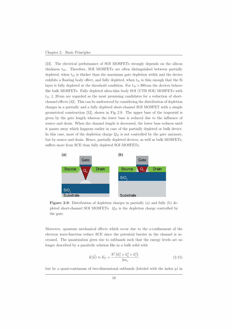
charges in a partially and a fully depleted short-channel SOI MOSFET with a simple
geometrical construction [52], shown in Fig. 2.9. The upper base of the trapezoid is
given by the gate length whereas the lower base is reduced due to the influence of
source and drain. When the channel length is decreased, the lower base reduces until
it passes away which happens earlier in case of the partially depleted or bulk device.
In this case, most of the depletion charge QD is not controlled by the gate anymore,
but by source and drain. Hence, partially depleted devices, as well as bulk MOSFETs,
suffers more from SCE than fully depleted SOI MOSFETs.
Figure 2.9: Distribution of depletion charges in partially (a) and fully (b) de-
pleted short-channel SOI MOSFETs. QD is the depletion charge controlled by
the gate.
Moreover, quantum mechanical effects which occur due to the z-confinement of the
electron wave-function reduce SCE since the potential barrier in the channel is in-
creased. The quantization gives rise to subbands such that the energy levels are no
longer described by a parabolic relation like in a bulk solid with
E(�k) ≈ EC +�
2(k2
x + k2y + k2
z
)2mc
(2.15)
but by a quasi-continuum of two-dimensional subbands (labeled with the index p) in
18
2.7. Parasitic Resistances and Capacitances
the channel that split up into energetically separated levels
Ep(kx, ky) ≈ EC + p2εz +�
2(k2
x + k2y
)2mc
εz =�
2π2
2mct2Si
(2.16)
The increase of the potential barrier in the channel is especially important for short-
channel MOSFETs with undoped channels to reduce short-channel effects and avoid
punch-through. Drawbacks of the quantization are a reduction of the density of states
in the channel and therefore a degradation of the MOSFET performance.
2.7 Parasitic Resistances and Capacitances
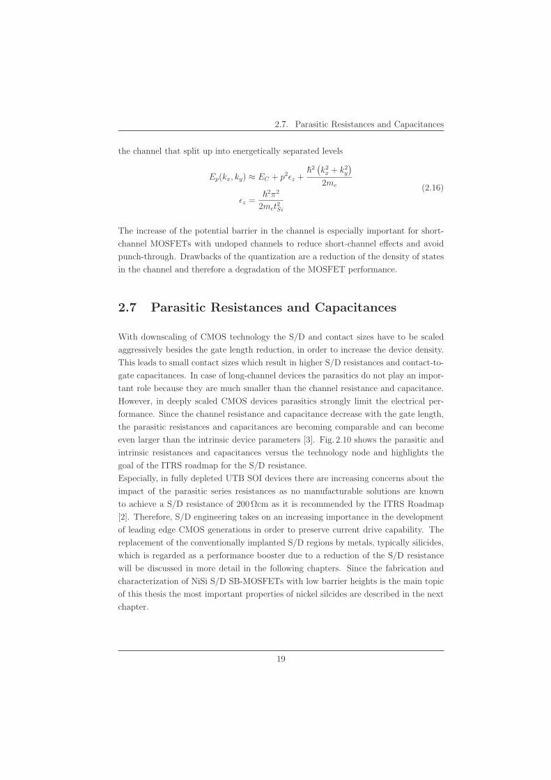
With downscaling of CMOS technology the S/D and contact sizes have to be scaled
aggressively besides the gate length reduction, in order to increase the device density.
This leads to small contact sizes which result in higher S/D resistances and contact-to-
gate capacitances. In case of long-channel devices the parasitics do not play an impor-
tant role because they are much smaller than the channel resistance and capacitance.
However, in deeply scaled CMOS devices parasitics strongly limit the electrical per-
formance. Since the channel resistance and capacitance decrease with the gate length,
the parasitic resistances and capacitances are becoming comparable and can become
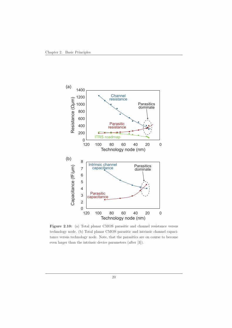
even larger than the intrinsic device parameters [3]. Fig. 2.10 shows the parasitic and
intrinsic resistances and capacitances versus the technology node and highlights the
goal of the ITRS roadmap for the S/D resistance.
Especially, in fully depleted UTB SOI devices there are increasing concerns about the
impact of the parasitic series resistances as no manufacturable solutions are known
to achieve a S/D resistance of 200 Ωcm as it is recommended by the ITRS Roadmap
[2]. Therefore, S/D engineering takes on an increasing importance in the development
of leading edge CMOS generations in order to preserve current drive capability. The
replacement of the conventionally implanted S/D regions by metals, typically silicides,
which is regarded as a performance booster due to a reduction of the S/D resistance
will be discussed in more detail in the following chapters. Since the fabrication and
characterization of NiSi S/D SB-MOSFETs with low barrier heights is the main topic
of this thesis the most important properties of nickel silcides are described in the next
chapter.
19
Chapter 2. Basic Principles
Technology node (nm)120 100 80 60 40 20 0
Technology node (nm)120 100 80 60 40 20 0
Res
ista
nce
(Ωμm
)
1400
1200
1000
800
600
400
200
0
Cap
acita
nce
(fF/μ
m)
8
76
5
4
3
20
Channelresistance
Intrinsic channelcapacitance
Parasiticresistance
Parasiticcapacitance
ITRS roadmap
Parasiticsdominate
Parasiticsdominate
(a)
(b)
Figure 2.10: (a) Total planar CMOS parasitic and channel resistance versus
technology node. (b) Total planar CMOS parasitic and intrinsic channel capaci-
tance versus technology node. Note, that the parasitics are on course to become
even larger than the intrinsic device parameters (after [3]).
20
Chapter 3
Nickel Silicide
This chapter briefly introduces nickel silicides and the advantages over other silicides
like TiSi2 and CoSi2. The formation of NiSi is presented and fabricated NiSi layers
on bulk Si and on SOI are investigated. The discussion of silicidation induced dopant
segregation completes this part.
3.1 Introduction
The use of metal silicides in Si technology is related to basic requirements like low spe-
cific resistivity, low contact resistivity to p-type and n-type Si, high thermal stability
and an excellent process compatibility with standard CMOS processing [53]. Nowa-
days, silicides are widely used as ohmic contacts, Schottky contacts and interconnects.
Moreover, as the parasitic series resistances increase with device dimension scaling,
as presented in Chapter 2.7, salicide (self-aligned silicide) processes have become an
indispensable technique for high-performance CMOS fabrication. The reduction of the
resistances is a major challenge, especially, for high-speed operation of digital circuits,
but also for high-frequency and low-noise operation of RF circuits.
Although, various silicides like TiSi2 and CoSi2 have been investigated as materials for
salicide processes, the midgap silicide NiSi offers major advantages for the sub-100 nm
node, e.g. low silicidation temperature, low silicon consumption, no bridging failure
property, smaller mechanical stress, no narrow-line effect on the sheet resistance and
smaller contact resistance [54].
Strong drawbacks of rare earth silicides like ErSi and YbSi are the difficult formation
and a Schottky barrier which is still too high. The disadvantage of PtSi are mainly the
high costs.
21
Chapter 3. Nickel Silicide
3.2 Formation of NiSi
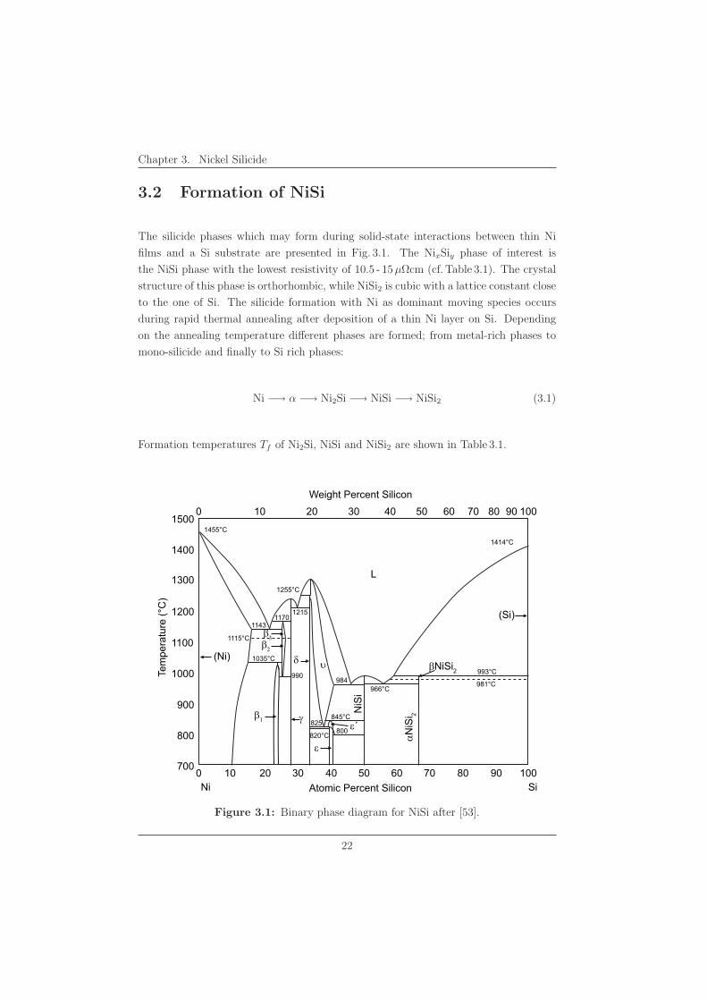
The silicide phases which may form during solid-state interactions between thin Ni
films and a Si substrate are presented in Fig. 3.1. The NixSiy phase of interest is
the NiSi phase with the lowest resistivity of 10.5 - 15μΩcm (cf. Table 3.1). The crystal
structure of this phase is orthorhombic, while NiSi2 is cubic with a lattice constant close
to the one of Si. The silicide formation with Ni as dominant moving species occurs
during rapid thermal annealing after deposition of a thin Ni layer on Si. Depending
on the annealing temperature different phases are formed; from metal-rich phases to
mono-silicide and finally to Si rich phases:
Ni −→ α −→ Ni2Si −→ NiSi −→ NiSi2 (3.1)
Formation temperatures Tf of Ni2Si, NiSi and NiSi2 are shown in Table 3.1.
1500
1400
1300
1200
1100
1000
900
800
700
Tem
pera
ture
(°C
)
Atomic Percent Silicon
Weight Percent Silicon
Ni Si0 10 20 30 40 50 60 70 80 90 100
0 10 20 30 40 50 60 80 9070 100
1414°C
1255°C
1455°C
1115°C
11431170
1215
990
800825
820°C
1035°C
993°C
981°C966°C
845°C
984
(Si)
(Ni)
L
βNiSi2υ
γ
ε
ε´
δ
β1
β2β3
αN
iSi 2N
iSi
Figure 3.1: Binary phase diagram for NiSi after [53].
22
3.2. Formation of NiSi
Phase Crystal Lattice constant (A) Tf ρ
structure a b c (◦C) (μΩcm)
Ni2Si Orthorhombic 5.00 3.73 7.04 200-325 24
NiSi Orthorhombic 5.18 3.34 5.62 350-600 10.5-15
NiSi2 Cubic 5.40 — — 750-800 34
Table 3.1: Properties of NixSiy phases [53]. Tf is the formation temperature; ρ
the specific resistance.
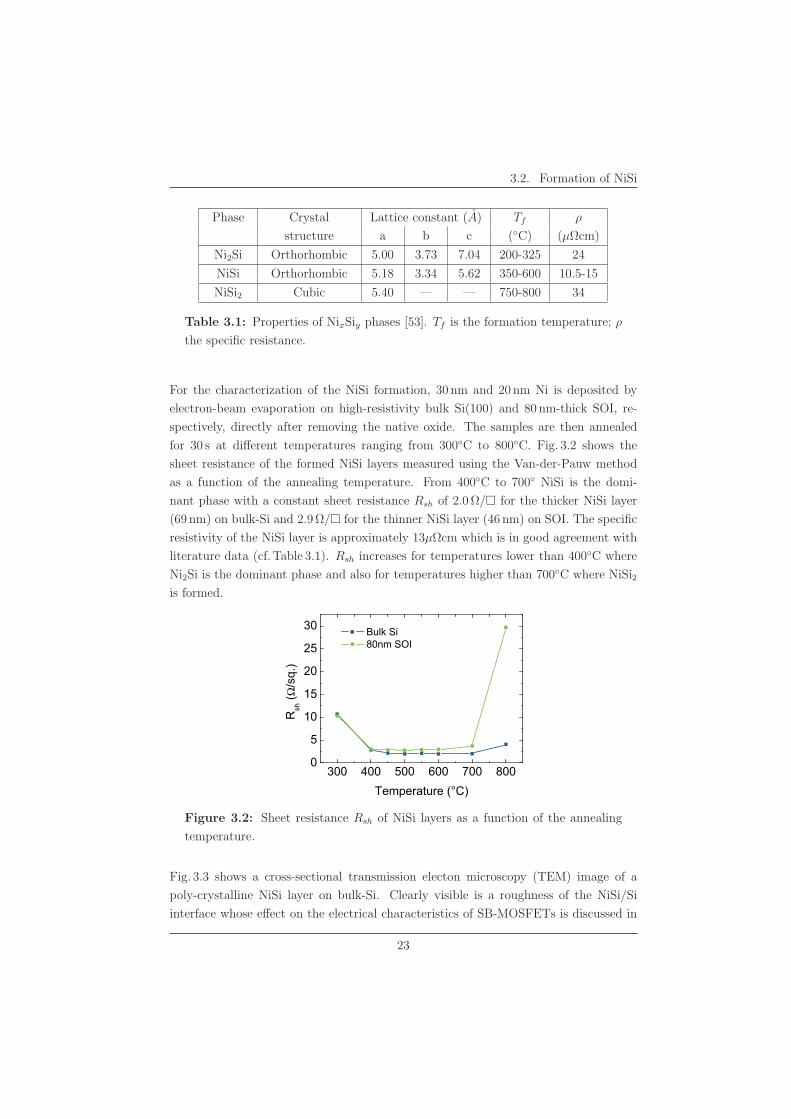
For the characterization of the NiSi formation, 30 nm and 20 nm Ni is deposited by
electron-beam evaporation on high-resistivity bulk Si(100) and 80 nm-thick SOI, re-
spectively, directly after removing the native oxide. The samples are then annealed
for 30 s at different temperatures ranging from 300◦C to 800◦C. Fig. 3.2 shows the
sheet resistance of the formed NiSi layers measured using the Van-der-Pauw method
as a function of the annealing temperature. From 400◦C to 700◦ NiSi is the domi-
nant phase with a constant sheet resistance Rsh of 2.0 Ω/� for the thicker NiSi layer
(69 nm) on bulk-Si and 2.9 Ω/� for the thinner NiSi layer (46 nm) on SOI. The specific
resistivity of the NiSi layer is approximately 13μΩcm which is in good agreement with
literature data (cf. Table 3.1). Rsh increases for temperatures lower than 400◦C where
Ni2Si is the dominant phase and also for temperatures higher than 700◦C where NiSi2
is formed.
300 400 500 600 700 8000
5
10
15
20
25
30
Rsh
(Ω/s
q.)
���������� �� �
��� �� ���� ���
Figure 3.2: Sheet resistance Rsh of NiSi layers as a function of the annealing
temperature.
Fig. 3.3 shows a cross-sectional transmission electon microscopy (TEM) image of a
poly-crystalline NiSi layer on bulk-Si. Clearly visible is a roughness of the NiSi/Si
interface whose effect on the electrical characteristics of SB-MOSFETs is discussed in
23
Chapter 3. Nickel Silicide
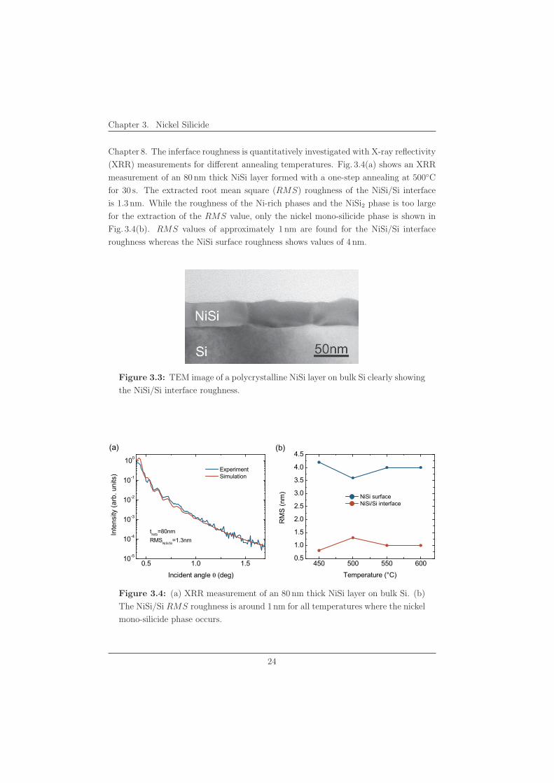
Chapter 8. The inferface roughness is quantitatively investigated with X-ray reflectivity
(XRR) measurements for different annealing temperatures. Fig. 3.4(a) shows an XRR
measurement of an 80 nm thick NiSi layer formed with a one-step annealing at 500◦C
for 30 s. The extracted root mean square (RMS) roughness of the NiSi/Si interface
is 1.3 nm. While the roughness of the Ni-rich phases and the NiSi2 phase is too large
for the extraction of the RMS value, only the nickel mono-silicide phase is shown in
Fig. 3.4(b). RMS values of approximately 1 nm are found for the NiSi/Si interface
roughness whereas the NiSi surface roughness shows values of 4 nm.
Figure 3.3: TEM image of a polycrystalline NiSi layer on bulk Si clearly showing
the NiSi/Si interface roughness.
450 500 550 6000.5
1.0
1.5
2.0
2.5
3.0
3.5
4.0
4.5
0.5 1.0 1.510-5
10-4
10-3
10-2
10-1
100
��� �
RM
S (n
m)
������ �� ����
� ����� � ����� �������� ��������
���
�
����������
����������
������
� !������� ��� "���#�
Inte
nsity
(arb
. uni
ts)
$���%���� ��&"�� θ� �%�&�
Figure 3.4: (a) XRR measurement of an 80 nm thick NiSi layer on bulk Si. (b)
The NiSi/Si RMS roughness is around 1 nm for all temperatures where the nickel
mono-silicide phase occurs.
24
3.3. Dopant Segregation
3.3 Dopant Segregation
During the silicide formation on doped Si, the dopants are found to redistribute at
the silicide/silicon interface. This concept of dopant segregation was introduced by R.
Thornten in 1981 who used a thin p-type interfacial layer to rise the PtSi Schottky
barrier on n-type Si [55]. During the silicidation induced dopant segregation, the
dopants are expected to be snow-plowed by the growing silicide and become piled-up
at the silicide/Si interface. Dopant segregation occurs if the solid solubility of the
dopants in the silicide is low and point defects exist at the silicide/Si interface [56]
and if the intrinsic diffusion of these dopants in Si is extremly low at the silicidation
temperatures (< 800◦C) [57]. A detailed description of the segregation mechanism can
be found in Ref. [56].
Figure 3.5: Schematic band diagrams of (a) a midgap silicide with equal Schot-
tky barrier heights for electrons and holes, (b) band bending induced by segre-
gated n-type dopants and (c) band bending induced by segregated p-type dopants
(after [58]). The n+ and p+ segregation layers are indicated by a blue and green
color gradient at the silicide/silicon interface.
The snow-plowed dopants in the silicon form a thin highly doped layer which causes a
strong up- or downward band bending depending on the type of dopants. As a conse-
quence, the tunneling probability of carriers through the effectively lowered Schottky
barrier increases significantly. Although, dopant segregation is performed at relatively
low temperatures, a fraction of dopants is located at substitutional sites in the silicon
lattice and is therefore activated. Recent theoretical investigations using first princi-
ples calculations suggest that dopants at substitutional sites in the silicon lattice at
the interface induce local dipoles which dominate the Schottky barrier height [20–22].
For instance, a B atom which is located at the substitutional site for a Si atom in the
Si layer induces interface dipoles in opposite direction to the electric dipoles generated
25
Chapter 3. Nickel Silicide
by the energy difference between the Femi level of NiSi and the charge neutrality level
of the semiconductor. As a result, the interface states, pinning the Fermi level, dis-
appear and the Fermi level shifts closer to the valence band edge due to the induced
dipoles around the B atom [20]. Consequently, the Schottky barrier height is reduced.
Fig. 3.5 shows schematically the strong band bending at the NiSi/Si interface for a
lightly doped n-type Si substrate with an n+ and a p+ segregation layer.
26
Chapter 4
Schottky-Diodes
A detailed analysis of the electrical characteristics of Schottky diodes is presented in this
chapter to provide the background for an understanding of SB-MOSFETs, where the
carrier injection is mediated by the source Schottky barrier. The physical background
of current transport in metal/semiconductor contacts and neccessary modifications of
the transport model for real applications are discussed. A systematic study of Schottky
barrier height modulation is carried out using silicidation induced dopant segregation
and the effective Schottky barrier heights are extracted as a function of the implantation
dose.
4.1 Ideal Metal-Semiconductor Contacts
A Schottky barrier is formed at a metal-semiconductor interface which controls the
current flow as well as the charge distribution of the contact. Fig. 4.1(a) shows ideal
energy-band diagrams of a seperated metal and an n-doped semiconductor. When
both materials are connected, which is illustrated in Fig. 4.1(b), charge will flow from
the semiconductor to the metal until thermal equilibrum is reached, i.e the Fermi level
of the metal EFm and of the semiconductor EFs line up. In this case, EFs is lowered
relative to EFm by an amount equal to the difference of the two workfunctions, resulting
in an upward band bending of the conduction and the valence bands.
Under these ideal conditions, the Schottky barrier height for electrons qΦ0Bn is simply
the difference between the metal workfunction qΦm and the electron affinity of the
semiconductor qχ:
qΦ0Bn = q (Φm − χ) (4.1)
27
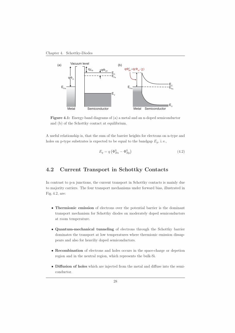
Chapter 4. Schottky-Diodes
(a) (b)
EFm
EFs
EV
EC
Vacuum level
qΦm
qχSi qΦCF
Metal Semiconductor
EFm EFs
EV
EC
qΦBn=q(Φm−χ)
Metal Semiconductor
0
Figure 4.1: Energy-band diagrams of (a) a metal and an n-doped semiconductor
and (b) of the Schottky contact at equilibrium.
A useful relationship is, that the sum of the barrier heights for electrons on n-type and
holes on p-type substrates is expected to be equal to the bandgap Eg, i. e.,
Eg = q(Φ0
Bn − Φ0Bp
)(4.2)
4.2 Current Transport in Schottky Contacts
In contrast to p-n junctions, the current transport in Schottky contacts is mainly due
to majority carriers. The four transport mechanisms under forward bias, illustrated in
Fig. 4.2, are:
• Thermionic emission of electrons over the potential barrier is the dominant
transport mechanism for Schottky diodes on moderately doped semiconductors
at room temperature.
• Quantum-mechanical tunneling of electrons through the Schottky barrier
dominates the transport at low temperatures where thermionic emission dissap-
pears and also for heaviliy doped semiconductors.
• Recombination of electrons and holes occurs in the space-charge or depetion
region and in the neutral region, which represents the bulk-Si.
• Diffusion of holes which are injected from the metal and diffuse into the semi-
conductor.
28
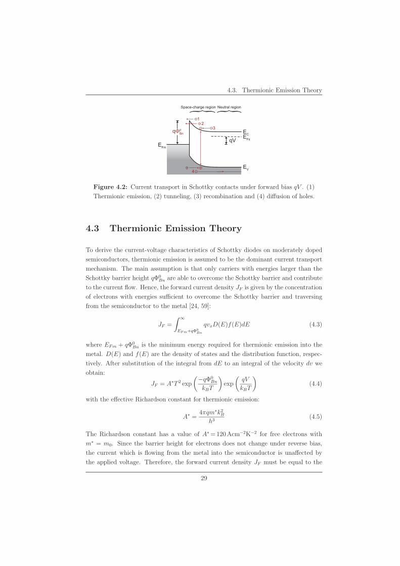
4.3. Thermionic Emission Theory
EFm
EFs
EV
EC
qV
12
3
4
} }Neutral regionSpace-charge region
qΦBn0
Figure 4.2: Current transport in Schottky contacts under forward bias qV . (1)
Thermionic emission, (2) tunneling, (3) recombination and (4) diffusion of holes.
4.3 Thermionic Emission Theory
To derive the current-voltage characteristics of Schottky diodes on moderately doped
semiconductors, thermionic emission is assumed to be the dominant current transport
mechanism. The main assumption is that only carriers with energies larger than the
Schottky barrier height qΦ0Bn are able to overcome the Schottky barrier and contribute
to the current flow. Hence, the forward current density JF is given by the concentration
of electrons with energies sufficient to overcome the Schottky barrier and traversing
from the semiconductor to the metal [24, 59]:
JF =
∫ ∞
EFm+qΦ0Bn
qvxD(E)f(E)dE (4.3)
where EFm + qΦ0Bn is the minimum energy required for thermionic emission into the
metal. D(E) and f(E) are the density of states and the distribution function, respec-
tively. After substitution of the integral from dE to an integral of the velocity dv we
obtain:
JF = A∗T 2 exp
(−qΦ0Bn
kBT
)exp
(qV
kBT
)(4.4)
with the effective Richardson constant for thermionic emission:
A∗ =4πqm∗k2
B
h3(4.5)
The Richardson constant has a value of A∗ = 120 Acm−2K−2 for free electrons with
m∗ = m0. Since the barrier height for electrons does not change under reverse bias,
the current which is flowing from the metal into the semiconductor is unaffected by
the applied voltage. Therefore, the forward current density JF must be equal to the
29
Chapter 4. Schottky-Diodes
reverse current density JR at thermal equilibrium, i. e., V = 0:
JR = −A∗T 2 exp
(−qΦ0Bn
kBT
)(4.6)
Finally, the total current for an area A is given by the sum of Eqs. 4.4 and 4.6.
I = IF − IR = I0
[exp
(qV
kBT
)− 1
](4.7)
with
I0 = AA∗T 2 exp
(−qΦ0Bn
kBT
)(4.8)
4.4 Real Metal-Semiconductor Contacts
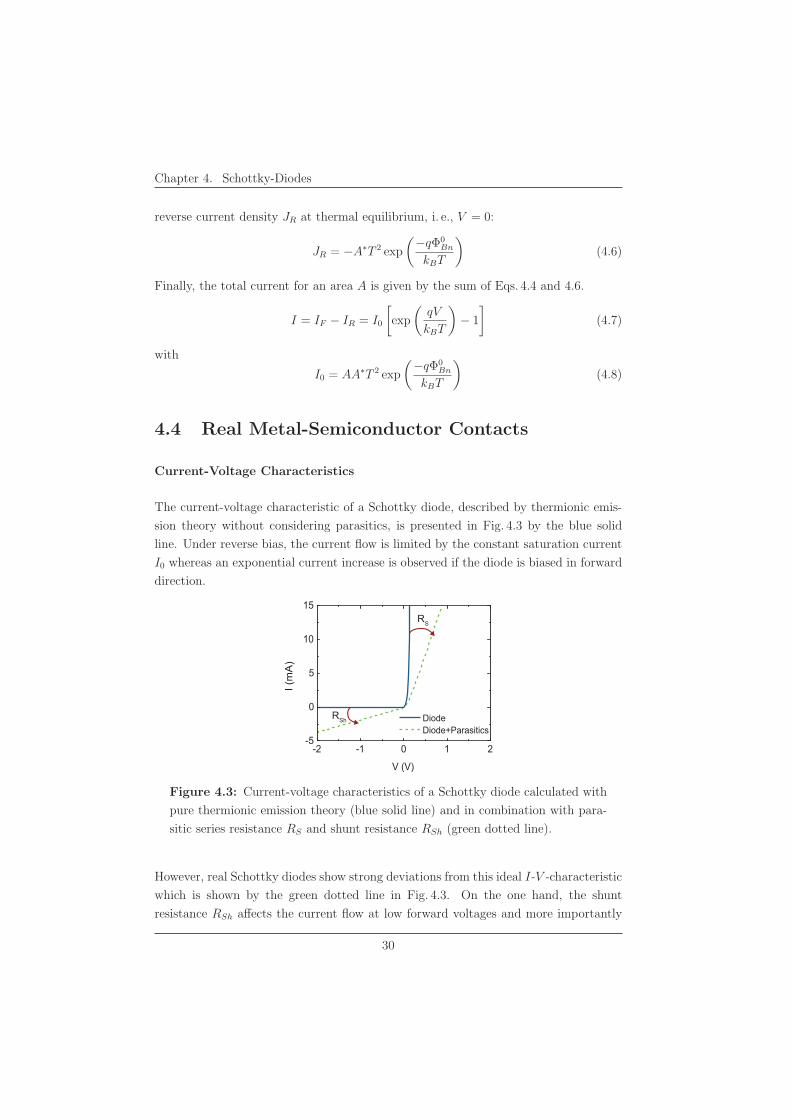
Current-Voltage Characteristics
The current-voltage characteristic of a Schottky diode, described by thermionic emis-
sion theory without considering parasitics, is presented in Fig. 4.3 by the blue solid
line. Under reverse bias, the current flow is limited by the constant saturation current
I0 whereas an exponential current increase is observed if the diode is biased in forward
direction.
-2 -1 0 1 2-5
0
5
10
15
I (m
A)
V (V)
Diode Diode+Parasitics
RS
RSh
Figure 4.3: Current-voltage characteristics of a Schottky diode calculated with
pure thermionic emission theory (blue solid line) and in combination with para-
sitic series resistance RS and shunt resistance RSh (green dotted line).
However, real Schottky diodes show strong deviations from this ideal I-V -characteristic
which is shown by the green dotted line in Fig. 4.3. On the one hand, the shunt
resistance RSh affects the current flow at low forward voltages and more importantly
30
4.4. Real Metal-Semiconductor Contacts
the reverse characteristics of diodes with high Schottky barrier height. On the other
hand, the parasitic series resistance RS changes the I-V characteristics, mostly at high
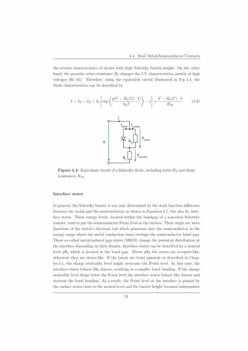
voltages [60, 61]. Therefore, using the equivalent circuit illustrated in Fig. 4.4, the
diode characteristics can be described by
I = IF − IR = I0
[exp
(q(V − RS(T ) · I)
kBT
)− 1
]+
V − RS(T ) · IRSh
(4.9)
I
Iparasitic
Vdiode
Vparasitic
V RSh
RS
Idiode
Figure 4.4: Equivalent circuit of a Schottky diode, including series RS and shunt
resistances RSh.
Interface states
In general, the Schottky barrier is not only determined by the work function difference
between the metal and the semiconductor as shown in Equation 4.1, but also by inter-
face states. These energy levels, located within the bandgap of a non-ideal Schottky
contact, tend to pin the semiconductor Fermi level at the surface. Their origin are wave
functions of the metal’s electrons tail which penetrate into the semiconductor in the
energy range where the metal conduction band overlaps the semiconductor band gap.
These so-called metal-induced gap states (MIGS) change the potential distribution at
the interface depending on their density. Interface states can be described by a neutral
level qΦ0 which is located in the band gap. Above qΦ0 the states are acceptor-like,
otherwise they are donor-like. If the bands are bend upwards as described in Chap-
ter 4.1, the charge neutrality level might overcome the Fermi level. In this case, the
interface states behave like donors, resulting in a smaller band bending. If the charge
neutrality level drops below the Fermi level the interface states behave like donors and
increase the band bending. As a result, the Fermi level at the interface is pinned by
the surface states close to the neutral level and the barrier height becomes independent
31
Chapter 4. Schottky-Diodes
of the work function difference:
qΦ0Bn = Eg − qΦ0 (4.10)
This description is only valid for Schottky diodes with a very high interface state
density (Dit → ∞). For metals on silicon, the Schottky barrier is determined by the
workfunction as well as the interface states.
Image-Force Lowering
An electron which is injected from the metal into the semiconductor induces a positive
image charge on the metal surface. The resulting attractive image force between the
electron and the equal positive image charge is proportional to 1/x2, where x is the
distance of the electron from the surface. In the presence of an external electric field
EM , the total electron energy E(x) is given by
E(x) = − q2
16πεSix− qEMx (4.11)
The image-force lowering ΔΦ is then given by the maximum of Equation 4.11, i. e.,
dE/dx = 0, or
ΔΦ =
√qEM
4πεSi
=
[q3N
8π2ε3Si
(Φ0
Bn − ΦCF + V)]1/4
(4.12)
Equation 4.12 shows, that barrier lowering depends on the doping concentration N of
the semiconductor, the difference between the conduction band edge and the Fermi
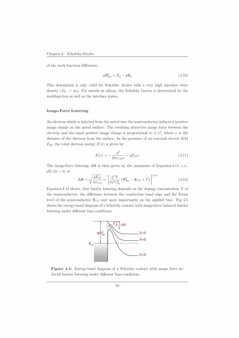
level of the semiconductor ΦCF and more importantly on the applied bias. Fig. 4.5
shows the energy-band diagram of a Schottky contact with image-force induced barrier
lowering under different bias conditions.
EFm
qΦBn
ΔΦ
V=0
V<0
V>00
Figure 4.5: Energy-band diagram of a Schottky contact with image force in-
duced barrier lowering under different bias conditions.
32
4.5. Extraction of the Schottky Barrier Height
Tunneling
As mentioned before, quantum-mechanical tunneling becomes significant for highly
doped semiconductors and at low temperatures. A good estimation of the tunneling
current can be obtained using the Wentzel-Kramers-Brillouin (WKB) approximation
for calculating the reverse current of Schottky diodes (cf. Chapter 4.5.2). A much easier
way which is often used is the incorporation of an ideality factor n, which modifies the
voltage dependency of Equation 4.7 to exp(
qVnkBT
). A strong drawback is that the
ideality factor is only defined for forward bias which is less affected by tunneling.
4.5 Extraction of the Schottky Barrier Height
For the extraction of Schottky barrier heights different techniques are usually employed.
Widely used are the capacitance-voltage [62], the current-voltage [63], the activation
energy [24, 64, 65] and the photoelectric method [66]. However, the most suitable for
the used test structures remains the activation energy technique since it is independent
of the electrically active area and it can be applied for diodes with very low Schottky
barrier heights [67]. Being independent of the mask designed area is very attractive to
study silicide-semiconductor interfaces because the electrical surface of carrier injection
can be different from this area. The method is more accurate in comparision to other
methods because of the use of a two-dimensional data set, I(V, T ), for the calculation
of Schottky barrier heights [68].
4.5.1 The Arrhenius Plot
Since the activation energy technique is used for the extraction of the Schottky barrier
heights of NiSi/Si diodes it is described in more detail here. The underlying Arrhenius
plot which is used for the extraction of the Schottky barrier height is a plot of ln(I/T 2)
versus 1/T at constant applied forward or reverse voltages. Assuming that the par-
asitic resistances can be negleted, the thermionic emission theory (Equation 4.7) can
be applied. Thus, the Arrhenius plot results in simple linear equations describing the
electrical characteristics of the diodes:
ln
∣∣∣∣ IR
T 2
∣∣∣∣ = ln AA∗ − 1
T· qΦ0
B
kB
for V < 0 (4.13)
ln
∣∣∣∣ IF
T 2
∣∣∣∣ = ln AA∗ − 1
T· q (Φ0
B + n−1V )
kB
for V > 0 (4.14)
33
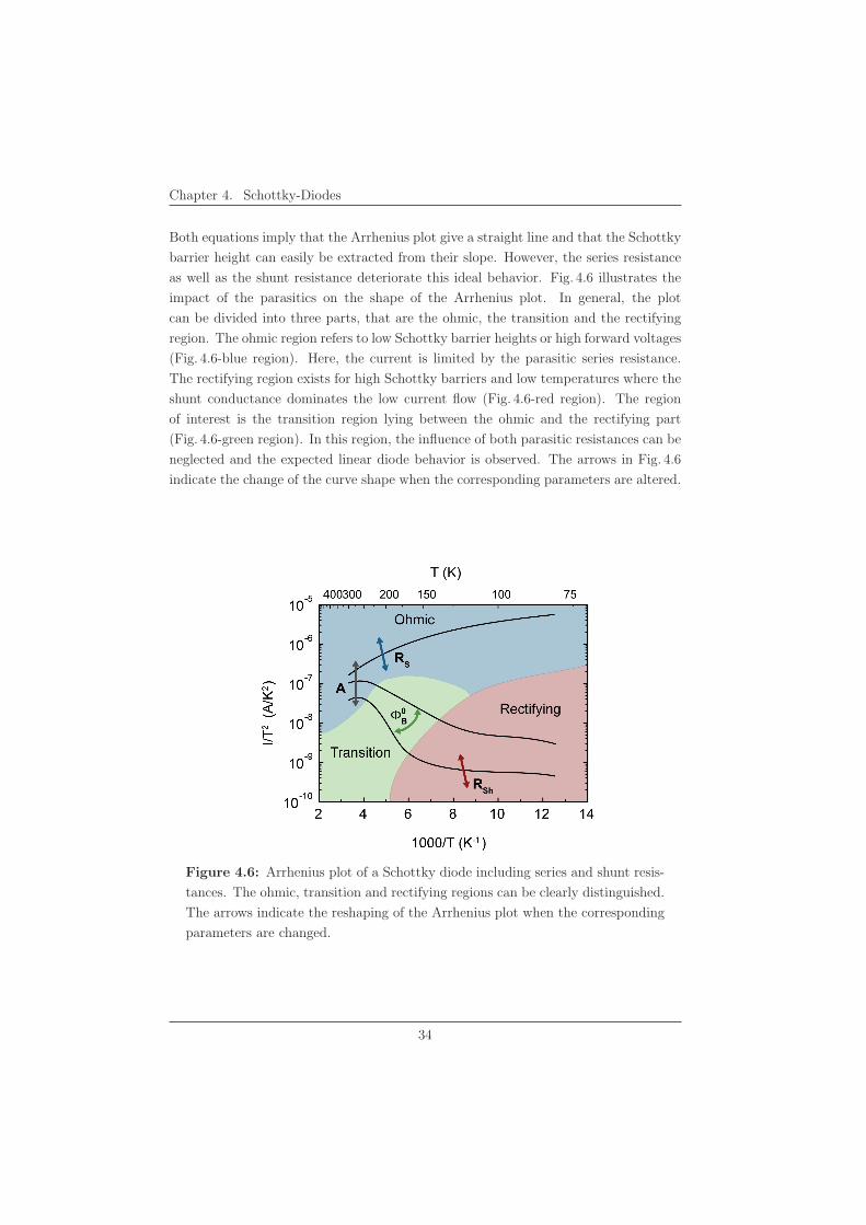
Chapter 4. Schottky-Diodes
Both equations imply that the Arrhenius plot give a straight line and that the Schottky
barrier height can easily be extracted from their slope. However, the series resistance
as well as the shunt resistance deteriorate this ideal behavior. Fig. 4.6 illustrates the
impact of the parasitics on the shape of the Arrhenius plot. In general, the plot
can be divided into three parts, that are the ohmic, the transition and the rectifying
region. The ohmic region refers to low Schottky barrier heights or high forward voltages
(Fig. 4.6-blue region). Here, the current is limited by the parasitic series resistance.
The rectifying region exists for high Schottky barriers and low temperatures where the
shunt conductance dominates the low current flow (Fig. 4.6-red region). The region
of interest is the transition region lying between the ohmic and the rectifying part
(Fig. 4.6-green region). In this region, the influence of both parasitic resistances can be
neglected and the expected linear diode behavior is observed. The arrows in Fig. 4.6
indicate the change of the curve shape when the corresponding parameters are altered.
Figure 4.6: Arrhenius plot of a Schottky diode including series and shunt resis-
tances. The ohmic, transition and rectifying regions can be clearly distinguished.
The arrows indicate the reshaping of the Arrhenius plot when the corresponding
parameters are changed.
34
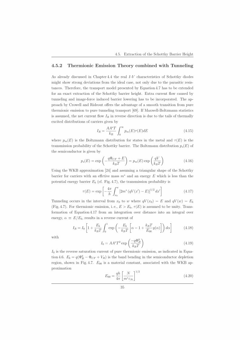
4.5. Extraction of the Schottky Barrier Height
4.5.2 Thermionic Emission Theory combined with Tunneling
As already discussed in Chapter 4.4 the real I-V characteristics of Schottky diodes
might show strong deviations from the ideal case, not only due to the parasitic resis-
tances. Therefore, the transport model presented by Equation 4.7 has to be extended
for an exact extraction of the Schottky barrier height. Extra current flow caused by
tunneling and image-force induced barrier lowering has to be incorporated. The ap-
proach by Crowell and Rideout offers the advantage of a smooth transition from pure
thermionic emission to pure tunneling transport [69]. If Maxwell-Boltzmann statistics
is assumed, the net current flow IR in reverse direction is due to the tails of thermally
excited distributions of carriers given by
IR =AA∗T
kB
∫ ∞
0
pm(E)τ(E)dE (4.15)
where pm(E) is the Boltzmann distribution for states in the metal and τ(E) is the
transmission probability of the Schottky barrier. The Boltzmann distribution ps(E) of
the semiconductor is given by
ps(E) = exp
(−qΦCF + E
kBT
)= pm(E) exp
(qV
kBT
)(4.16)
Using the WKB approximation [24] and assuming a triangular shape of the Schottky
barrier for carriers with an effctive mass m∗ and an energy E which is less than the
potential energy barrier Eb (cf. Fig. 4.7), the transmission probability is
τ(E) = exp
[−4π
h
∫ w
x0
[2m∗ (qV (x′) − E)]1/2
dx′]
(4.17)
Tunneling occurs in the interval from x0 to w where qV (x0) = E and qV (w) = Eb
(Fig. 4.7). For thermionic emission, i. e., E > Eb, τ(E) is assumed to be unity. Trans-
formation of Equation 4.17 from an integration over distance into an integral over
energy, α ≡ E/Eb, results in a reverse current of
IR = I0
[1 +
Eb
kBT
∫ 1
0
exp
(− Eb
kBT
[α − 1 +
kBT
E00
y(α)
])dα
](4.18)
with
I0 = AA∗T 2 exp
(−qΦ0B
kBT
)(4.19)
I0 is the reverse saturation current of pure thermionic emission, as indicated in Equa-
tion 4.6. Eb = q(Φ0B − ΦCF + VR) is the band bending in the semiconductor depletion
region, shown in Fig. 4.7. E00 is a material constant, associated with the WKB ap-
proximation
E00 =qh
4π
[N
m∗εSi
]1/2
(4.20)
35
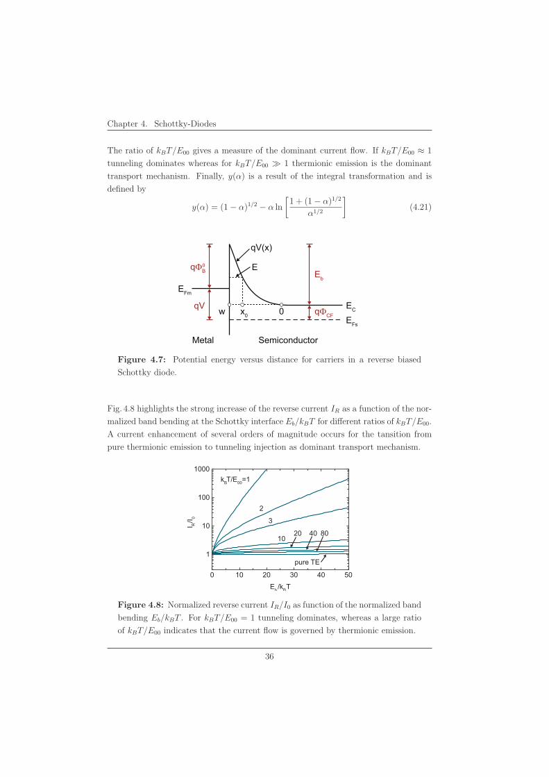
Chapter 4. Schottky-Diodes
The ratio of kBT/E00 gives a measure of the dominant current flow. If kBT/E00 ≈ 1
tunneling dominates whereas for kBT/E00 1 thermionic emission is the dominant
transport mechanism. Finally, y(α) is a result of the integral transformation and is
defined by
y(α) = (1 − α)1/2 − α ln
[1 + (1 − α)1/2
α1/2
](4.21)
EFm
EFs
Eb
qV
qV(x)
qΦCF
EC
qΦB
Metal Semiconductor
0 E
0x0w
Figure 4.7: Potential energy versus distance for carriers in a reverse biased
Schottky diode.
Fig. 4.8 highlights the strong increase of the reverse current IR as a function of the nor-
malized band bending at the Schottky interface Eb/kBT for different ratios of kBT/E00.
A current enhancement of several orders of magnitude occurs for the tansition from
pure thermionic emission to tunneling injection as dominant transport mechanism.
0 10 20 30 40 50
1
10
100
1000
8020 4010
2
I R/I 0
Eb /kBT
kBT/E00=1
pure TE
3
Figure 4.8: Normalized reverse current IR/I0 as function of the normalized band
bending Eb/kBT . For kBT/E00 = 1 tunneling dominates, whereas a large ratio
of kBT/E00 indicates that the current flow is governed by thermionic emission.
36
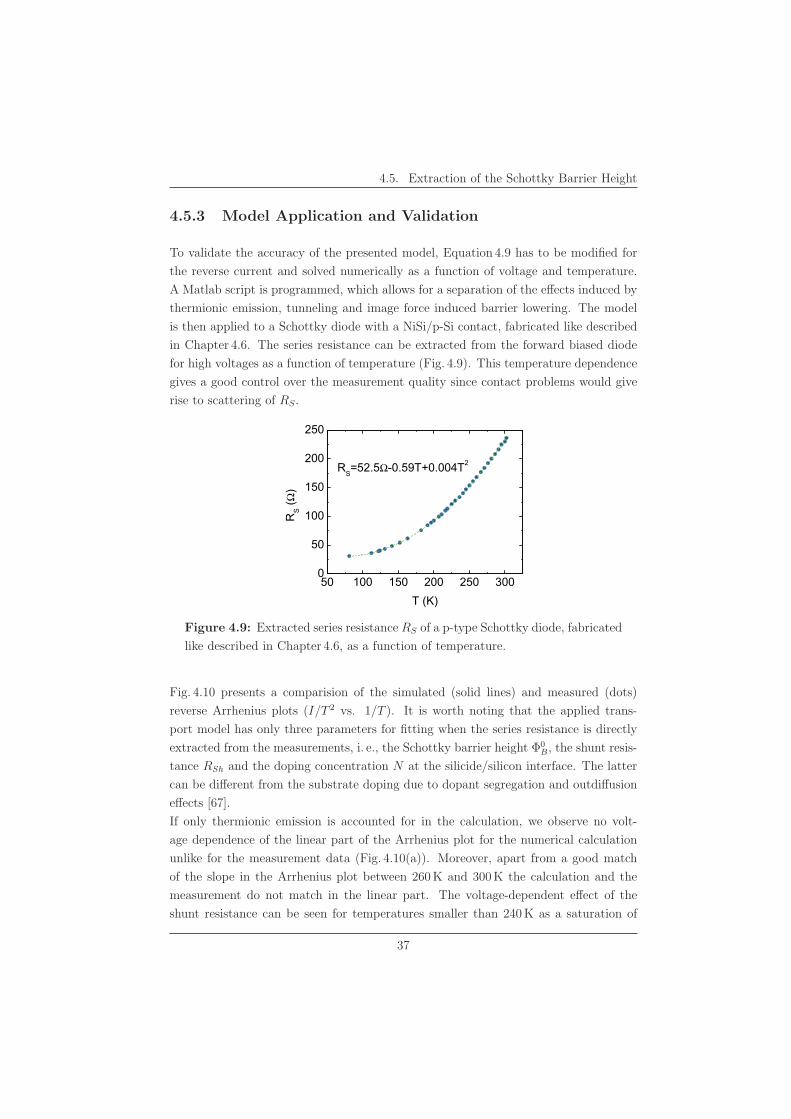
4.5. Extraction of the Schottky Barrier Height
4.5.3 Model Application and Validation
To validate the accuracy of the presented model, Equation 4.9 has to be modified for
the reverse current and solved numerically as a function of voltage and temperature.
A Matlab script is programmed, which allows for a separation of the effects induced by
thermionic emission, tunneling and image force induced barrier lowering. The model
is then applied to a Schottky diode with a NiSi/p-Si contact, fabricated like described
in Chapter 4.6. The series resistance can be extracted from the forward biased diode
for high voltages as a function of temperature (Fig. 4.9). This temperature dependence
gives a good control over the measurement quality since contact problems would give
rise to scattering of RS.
50 100 150 200 250 3000
50
100
150
200
250
RS (Ω
)
T (K)
RS=52.5Ω-0.59T+0.004T2
Figure 4.9: Extracted series resistance RS of a p-type Schottky diode, fabricated
like described in Chapter 4.6, as a function of temperature.
Fig. 4.10 presents a comparision of the simulated (solid lines) and measured (dots)
reverse Arrhenius plots (I/T 2 vs. 1/T ). It is worth noting that the applied trans-
port model has only three parameters for fitting when the series resistance is directly
extracted from the measurements, i. e., the Schottky barrier height Φ0B, the shunt resis-
tance RSh and the doping concentration N at the silicide/silicon interface. The latter
can be different from the substrate doping due to dopant segregation and outdiffusion
effects [67].
If only thermionic emission is accounted for in the calculation, we observe no volt-
age dependence of the linear part of the Arrhenius plot for the numerical calculation
unlike for the measurement data (Fig. 4.10(a)). Moreover, apart from a good match
of the slope in the Arrhenius plot between 260 K and 300 K the calculation and the
measurement do not match in the linear part. The voltage-dependent effect of the
shunt resistance can be seen for temperatures smaller than 240 K as a saturation of
37
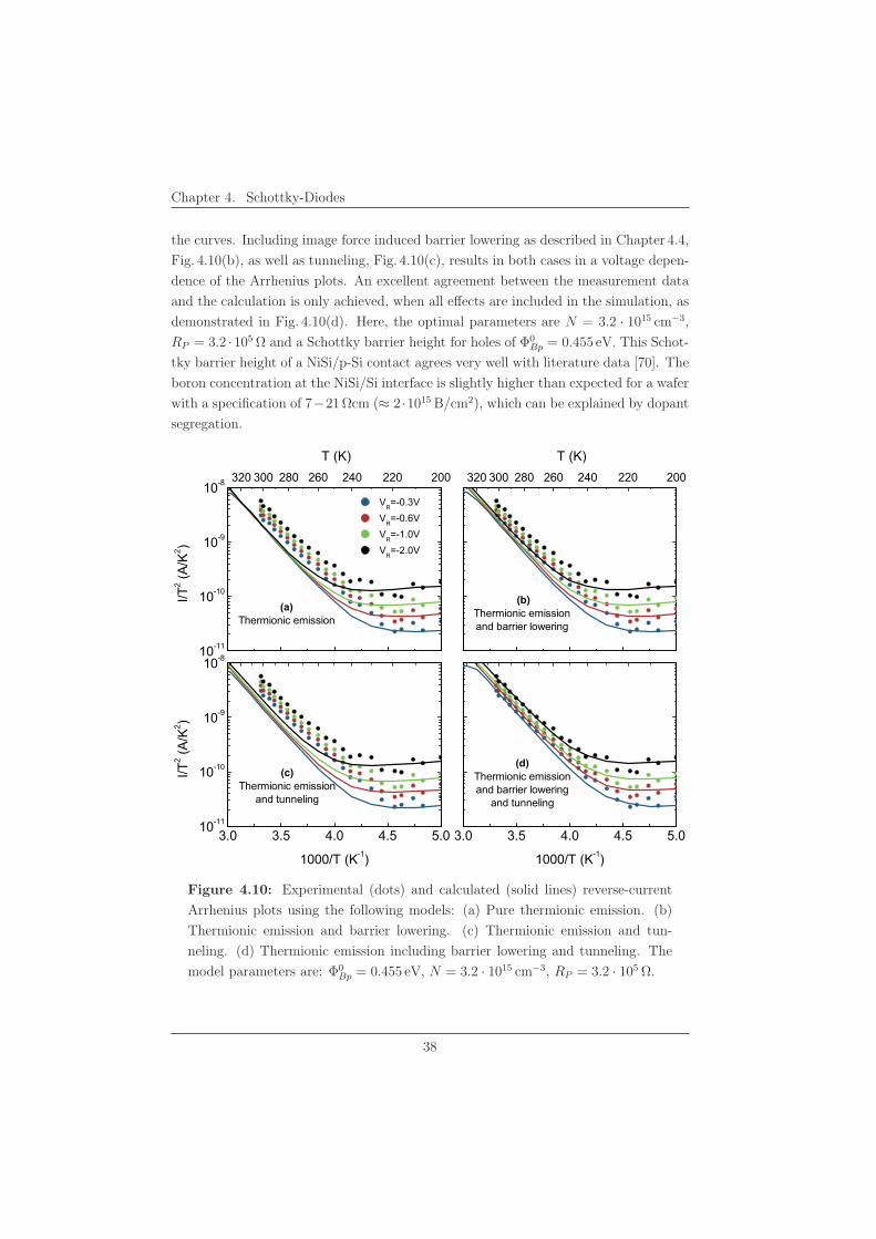
Chapter 4. Schottky-Diodes
the curves. Including image force induced barrier lowering as described in Chapter 4.4,
Fig. 4.10(b), as well as tunneling, Fig. 4.10(c), results in both cases in a voltage depen-
dence of the Arrhenius plots. An excellent agreement between the measurement data
and the calculation is only achieved, when all effects are included in the simulation, as
demonstrated in Fig. 4.10(d). Here, the optimal parameters are N = 3.2 · 1015 cm−3,
RP = 3.2 ·105 Ω and a Schottky barrier height for holes of Φ0Bp = 0.455 eV. This Schot-
tky barrier height of a NiSi/p-Si contact agrees very well with literature data [70]. The
boron concentration at the NiSi/Si interface is slightly higher than expected for a wafer
with a specification of 7−21 Ωcm (≈ 2 ·1015 B/cm2), which can be explained by dopant
segregation.
10-11
10-10
10-9
10-8
3.0 3.5 4.0 4.5 5.010-11
10-10
10-9
10-8
3.0 3.5 4.0 4.5 5.0
VR=-0.3V VR=-0.6V VR=-1.0V VR=-2.0V
I/T2 (A
/K2 )
320 300 280 260 240 220 200
(d)Thermionic emissionand barrier lowering
and tunneling
(c)Thermionic emission
and tunneling
(b)Thermionic emission and barrier lowering
T (K)
(a)Thermionic emission
320 300 280 260 240 220 200
T (K)
I/T2 (A
/K2 )
1000/T (K-1)
1000/T (K-1)
Figure 4.10: Experimental (dots) and calculated (solid lines) reverse-current
Arrhenius plots using the following models: (a) Pure thermionic emission. (b)
Thermionic emission and barrier lowering. (c) Thermionic emission and tun-
neling. (d) Thermionic emission including barrier lowering and tunneling. The
model parameters are: Φ0Bp = 0.455 eV, N = 3.2 · 1015 cm−3, RP = 3.2 · 105 Ω.
38
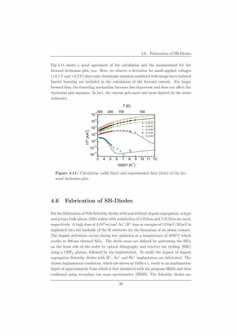
4.6. Fabrication of SB-Diodes
Fig. 4.11 shows a good agreement of the calculation and the measurement for the
forward Arrhenius plot, too. Here, we observe a deviation for small applied voltages
(+0.1 V and +0.3 V) since only thermionic emission combined with image force induced
barrier lowering are included in the calculation of the forward current. For larger
forward bias, the tunneling mechanism becomes less important and does not affect the
Arrhenius plot anymore. In fact, the current gets more and more limited by the series
resistance.
3 4 5 6 7 8 9 10 11 1210-11
10-10
10-9
10-8
10-7
10-6
10-5
VF=0.1V
VF=0.3V
VF=0.6V
VF=1.0V
VF=2.0V
I/T2 (A
/K2 )
1000/T (K-1)
300 200 100
T (K)
150
Figure 4.11: Calculation (solid lines) and experimental data (dots) of the for-
ward Arrhenius plot.
4.6 Fabrication of SB-Diodes
For the fabrication of NiSi Schottky diodes with and without dopant segregation, n-type
and p-type bulk silicon (100) wafers with resistivities of 1-8 Ωcm and 7-21 Ωcm are used,
respectively. A high dose of 3·1015at/cm2 As+/B+ ions at energies of 115 keV/20 keV is
implanted into the backside of the Si substrate for the formation of an ohmic contact.
The dopant activation occurs during wet oxidation at a temperature of 1050◦C which
results in 300 nm thermal SiO2. The diode areas are defined by patterning the SiO2
on the front side of the wafer by optical lithography and reactive ion etching (RIE)
using a CHF3 plasma, followed by ion implantation. To study the impact of dopant
segregation Schottky diodes with B+, As+ and Sb+ implantation are fabricated. The
chosen implantation conditions, which are shown in Table 4.1, result in an implantation
depth of approximately 8 nm which is first simulated with the program SRIM and then
confirmed using secondary ion mass spectrometry (SIMS). The Schottky diodes are
39
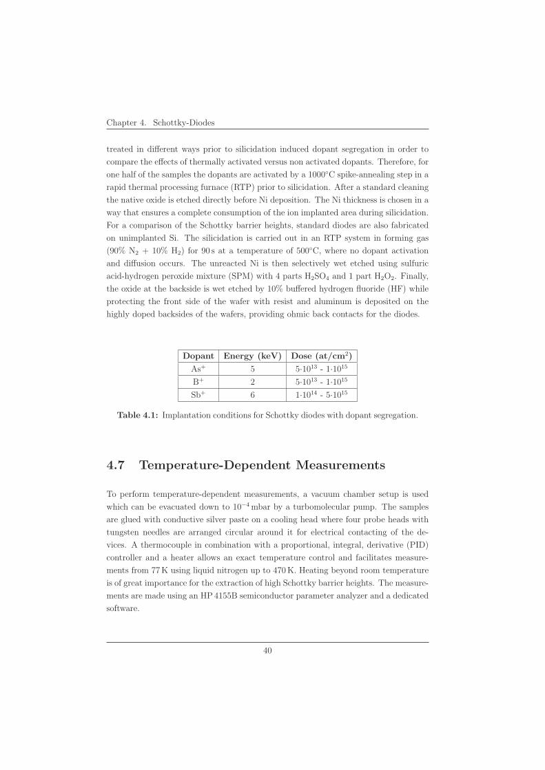
Chapter 4. Schottky-Diodes
treated in different ways prior to silicidation induced dopant segregation in order to
compare the effects of thermally activated versus non activated dopants. Therefore, for
one half of the samples the dopants are activated by a 1000◦C spike-annealing step in a
rapid thermal processing furnace (RTP) prior to silicidation. After a standard cleaning
the native oxide is etched directly before Ni deposition. The Ni thickness is chosen in a
way that ensures a complete consumption of the ion implanted area during silicidation.
For a comparison of the Schottky barrier heights, standard diodes are also fabricated
on unimplanted Si. The silicidation is carried out in an RTP system in forming gas
(90% N2 + 10% H2) for 90 s at a temperature of 500◦C, where no dopant activation
and diffusion occurs. The unreacted Ni is then selectively wet etched using sulfuric
acid-hydrogen peroxide mixture (SPM) with 4 parts H2SO4 and 1 part H2O2. Finally,
the oxide at the backside is wet etched by 10% buffered hydrogen fluoride (HF) while
protecting the front side of the wafer with resist and aluminum is deposited on the
highly doped backsides of the wafers, providing ohmic back contacts for the diodes.
Dopant Energy (keV) Dose (at/cm2)
As+ 5 5·1013 - 1·1015
B+ 2 5·1013 - 1·1015
Sb+ 6 1·1014 - 5·1015
Table 4.1: Implantation conditions for Schottky diodes with dopant segregation.
4.7 Temperature-Dependent Measurements
To perform temperature-dependent measurements, a vacuum chamber setup is used
which can be evacuated down to 10−4 mbar by a turbomolecular pump. The samples
are glued with conductive silver paste on a cooling head where four probe heads with
tungsten needles are arranged circular around it for electrical contacting of the de-
vices. A thermocouple in combination with a proportional, integral, derivative (PID)
controller and a heater allows an exact temperature control and facilitates measure-
ments from 77 K using liquid nitrogen up to 470 K. Heating beyond room temperature
is of great importance for the extraction of high Schottky barrier heights. The measure-
ments are made using an HP 4155B semiconductor parameter analyzer and a dedicated
software.
40
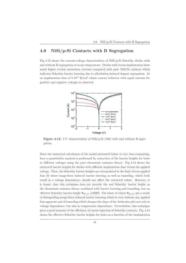
4.8. NiSi/p-Si Contacts with B Segregation
4.8 NiSi/p-Si Contacts with B Segregation
Fig. 4.12 shows the current-voltage characteristics of NiSi/p-Si Schottky diodes with
and without B segregation at room temperature. Diodes with boron implantation show
much higher reverse saturation currents compared with pure NiSi/Si contacts which
indicates Schottky barrier lowering due to silicidation induced dopant segregation. At
an implantation dose of 5·1014 B/cm2 ohmic contact behavior with equal currents for
positive and negative voltages is observed.
-2 -1 0 1 210-6
10-5
10-4
10-3
10-2
Cur
rent
(A)
Voltage (V)
w/o implantation 5x10¹³ B/cm2
1x10¹⁴ B/cm2
5x10¹⁴ B/cm2
1x10¹⁵ B/cm2
Figure 4.12: I-V characteristics of NiSi/p-Si (100) with and without B segre-
gation.
Since the numerical calculation of the model presented before is very time-consuming,
here a quantitative analysis is performed by extraction of the barrier heights for holes
at different voltages using the pure thermionic emission theory. Fig. 4.13 shows the
extracted barrier heights for diodes with different implantation dose versus the applied
voltage. Then, the Schottky barrier heights are extrapolated in the limit of zero applied
bias [9] where image-force induced barrier lowering as well as tunneling, which both
result in a voltage dependency, should not affect the extracted values. However, it
is found, that this technique does not provide the real Schottky barrier height as
the thermionic emission theory combined with barrier lowering and tunneling, but an
effective Schottky barrier height ΦB,eff (eSBH). The lower of values ΦB,eff are a result
of disregarding image-force induced barrier lowering which is even without any applied
bias apparent and of tunneling which changes the slope of the Arrhenius plot not only in
voltage dependence, but also in temperature dependence. Nevertheless, this technique
gives a good measure of the efficiency of carrier injection of Schottky contacts. Fig. 4.14
shows the effective Schottky barrier heights for holes as a function of the implantation
41
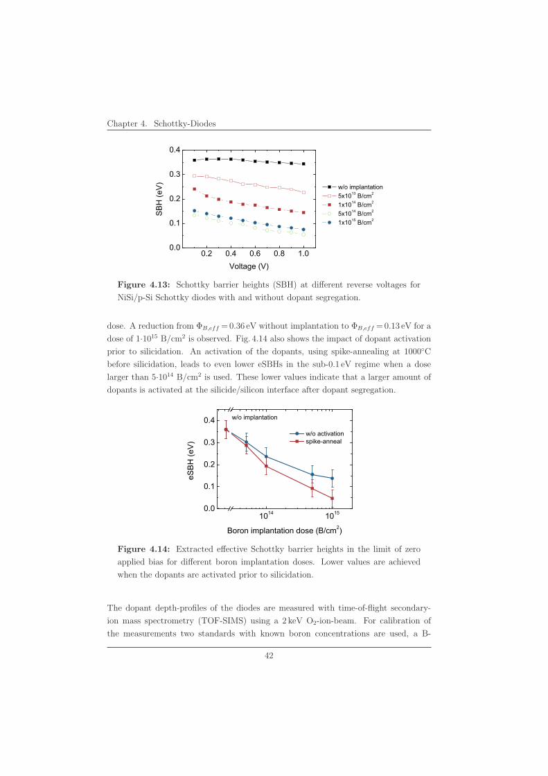
Chapter 4. Schottky-Diodes
0.2 0.4 0.6 0.8 1.00.0
0.1
0.2
0.3
0.4
w/o implantation 5x10¹³ B/cm2
1x10¹⁴ B/cm2
5x10¹⁴ B/cm2
1x10¹⁵ B/cm2
SB
H (e
V)
Voltage (V)
Figure 4.13: Schottky barrier heights (SBH) at different reverse voltages for
NiSi/p-Si Schottky diodes with and without dopant segregation.
dose. A reduction from ΦB,eff = 0.36 eV without implantation to ΦB,eff = 0.13 eV for a
dose of 1·1015 B/cm2 is observed. Fig. 4.14 also shows the impact of dopant activation
prior to silicidation. An activation of the dopants, using spike-annealing at 1000◦C
before silicidation, leads to even lower eSBHs in the sub-0.1 eV regime when a dose
larger than 5·1014 B/cm2 is used. These lower values indicate that a larger amount of
dopants is activated at the silicide/silicon interface after dopant segregation.
1014 10150.0
0.1
0.2
0.3
0.4
eSB
H (e
V)
Boron implantation dose (B/cm2)
w/o activation spike-anneal
w/o implantation
Figure 4.14: Extracted effective Schottky barrier heights in the limit of zero
applied bias for different boron implantation doses. Lower values are achieved
when the dopants are activated prior to silicidation.
The dopant depth-profiles of the diodes are measured with time-of-flight secondary-
ion mass spectrometry (TOF-SIMS) using a 2 keV O2-ion-beam. For calibration of
the measurements two standards with known boron concentrations are used, a B-
42
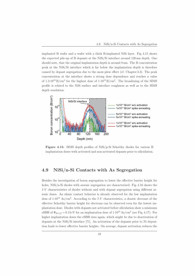
4.9. NiSi/n-Si Contacts with As Segregation
implanted Si wafer and a wafer with a thick B-implanted NiSi layer. Fig. 4.15 shows
the expected pile-up of B dopants at the NiSi/Si interface around 120 nm depth. One
should note, that the original implantation depth is around 8 nm. The B concentration
peak at the NiSi/Si interface which is far below the implantation depth is therefore
caused by dopant segregation due to the snow-plow effect (cf. Chapter 3.3). The peak
concentration at the interface shows a strong dose dependence and reaches a value
of 1.3·1019 B/cm3 for the highest dose of 1·1015 B/cm2. The broadening of the SIMS
profile is related to the NiSi surface and interface roughness as well as to the SIMS
depth resolution.
1017
1018
1019
Bor
on c
once
ntra
tion
(B/c
m3 )
1x10¹⁴ B/cm2 w/o activation1x1014 B/cm2 spike-annealing
5x10¹⁴ B/cm2 w/o activation5x1014 B/cm2 spike-annealing
1x10¹⁵ B/cm2 w/o activation1x1015 B/cm2 spike-annealing
NiSi/Si interface
0 40 80 120 160 200Depth (nm)
Figure 4.15: SIMS depth profiles of NiSi/p-Si Schottky diodes for various B
implantation doses with activated and non-activated dopants prior to silicidation.
4.9 NiSi/n-Si Contacts with As Segregation
Besides the investigation of boron segregation to lower the effective barrier height for
holes, NiSi/n-Si diodes with arsenic segregation are characterized. Fig. 4.16 shows the
I-V characteristics of diodes without and with dopant segregation using different ar-
senic doses. An ohmic contact behavior is already observed for the low implantation
dose of 1·1014 As/cm2. According to the I-V characteristics, a drastic decrease of the
effective Schottky barrier height for electrons can be observed even for the lowest im-
plantation dose. Diodes with dopants not activated before silicidation show a minimum
eSBH of ΦB,eff = 0.13 eV for an implantation dose of 1·1015 As/cm2 (see Fig. 4.17). For
higher implantation doses the eSBH rises again, which might be due to deactivation of
dopants at the NiSi/Si interface [71]. An activation of the dopants prior to Ni deposi-
tion leads to lower effective barrier heights. On average, dopant activation reduces the
43
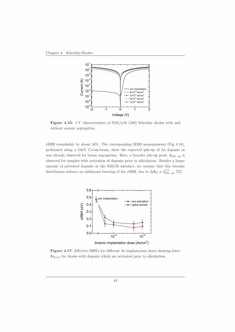
Chapter 4. Schottky-Diodes
-2 -1 0 1 210-910-810-710-610-510-410-310-210-1
w/o implantation 5x10¹³ As/cm2
1x10¹⁴ As/cm2
5x10¹⁴ As/cm2
1x10¹⁵ As/cm2
Cur
rent
(A)
Voltage (V)
Figure 4.16: I-V characteristics of NiSi/n-Si (100) Schottky diodes with and
without arsenic segregation.
eSBH remarkably by about 34%. The corresponding SIMS measurements (Fig. 4.18),
performed using a 2 keV Cs-ion-beam, show the expected pile-up of As dopants as
was already observed for boron segregation. Here, a broader pile-up peak, dPile−up is
observed for samples with activation of dopants prior to silicidation. Besides a larger
amount of activated dopants at the NiSi/Si interface, we assume that this broader
distribution induces an additional lowering of the eSBH, due to ΔΦB ∝ d1/2Pile−up [72].
1014 10150.0
0.1
0.2
0.3
0.4
0.5
0.6
w/o implantation
eSB
H (e
V)
Arsenic implantation dose (As/cm2)
w/o activation spike-anneal
Figure 4.17: Effective SBH’s for different As implantation doses showing lower
ΦB,eff for diodes with dopants which are activated prior to silicidation.
44
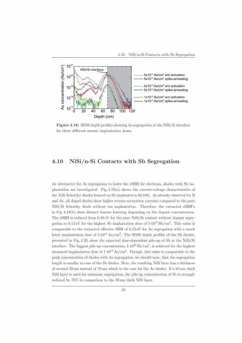
4.10. NiSi/n-Si Contacts with Sb Segregation
0 20 40 60 80 100 1201017
1018
1019
1020
1021A
s co
ncen
tratio
n (A
s/cm
3 )
Depth (nm)
5x10¹³ As/cm2 w/o activation5x1013 As/cm2 spike-annealing
5x10¹⁴ As/cm2 w/o activation5x1014 As/cm2 spike-annealing
1x10¹⁵ As/cm2 w/o activation1x1015 As/cm2 spike-annealing
NiSi/Si interface
Figure 4.18: SIMS depth profiles showing As segregation at the NiSi/Si interface
for three different arsenic implantation doses.
4.10 NiSi/n-Si Contacts with Sb Segregation
As alternative for As segregation to lower the eSBH for electrons, diodes with Sb im-
plantation are investigated. Fig. 4.19(a) shows the current-voltage characteristics of
the NiSi Schottky diodes formed on Sb implanted n-Si(100). As already observed for B
and As, all doped diodes show higher reverse saturation currents compared to the pure
NiSi/Si Schottky diode without ion implantation. Therefore, the extracted eSBH’s
in Fig. 4.19(b) show distinct barrier lowering depending on the dopant concentration.
The eSBH is reduced from 0.48 eV for the pure NiSi/Si contact without dopant segre-
gation to 0.13 eV for the highest Sb implantation dose of 5·1015 Sb/cm2. This value is
comparable to the extracted effective SBH of 0.13 eV for As segregation with a much
lower implantation dose of 5·1014 As/cm2. The SIMS depth profiles of the Sb diodes,
presented in Fig. 4.20, show the expected dose-dependent pile-up of Sb at the NiSi/Si
interface. The biggest pile-up concentration, 1·1020 Sb/cm3, is achieved for the highest
measured implantation dose of 1·1015 As/cm2. Though, this value is comparable to the
peak concentration of diodes with As segregation, we should note, that the segregation
length is smaller in case of the Sb diodes. Here, the resulting NiSi layer has a thickness
of around 39 nm instead of 70 nm which is the case for the As diodes. If a 65 nm thick
NiSi layer is used for antimony segregation, the pile-up concentration of Sb is strongly
reduced by 70% in comparison to the 39 nm thick NiSi layer.
45
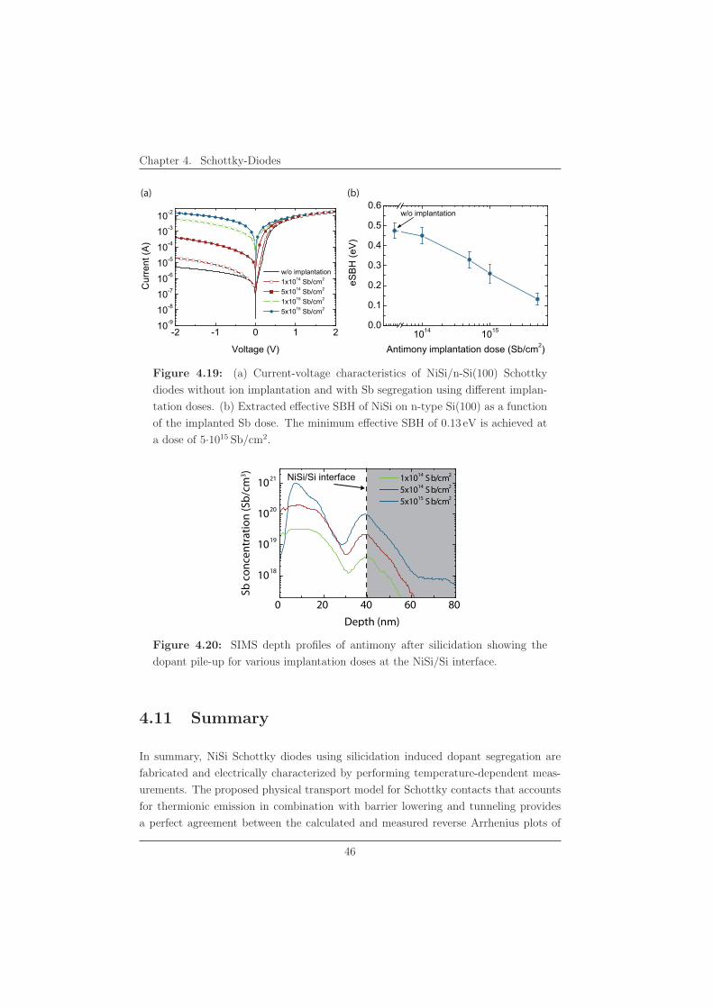
Chapter 4. Schottky-Diodes
-2 -1 0 1 210-9
10-8
10-7
10-6
10-5
10-4
10-3
10-2
Cur
rent
(A)
Voltage (V)
w/o implantation 1x10¹⁴ Sb/cm2
5x10¹⁴ Sb/cm2
1x10¹⁵ Sb/cm2
5x10¹⁵ Sb/cm2
1014 10150.0
0.1
0.2
0.3
0.4
0.5
0.6
eSB
H (e
V)
Antimony implantation dose (Sb/cm2)
w/o implantation
(a) (b)
Figure 4.19: (a) Current-voltage characteristics of NiSi/n-Si(100) Schottky
diodes without ion implantation and with Sb segregation using different implan-
tation doses. (b) Extracted effective SBH of NiSi on n-type Si(100) as a function
of the implanted Sb dose. The minimum effective SBH of 0.13 eV is achieved at
a dose of 5·1015 Sb/cm2.
0 20 40 60 80
1018
1019
1020
1021
Sb c
once
ntra
tion
(Sb/
cm3 )
Depth (nm)
1x10¹⁴ S b/cm2
5x10¹⁴ S b/cm2
5x10¹⁵ S b/cm2
NiSi/Si interface
Figure 4.20: SIMS depth profiles of antimony after silicidation showing the
dopant pile-up for various implantation doses at the NiSi/Si interface.
4.11 Summary
In summary, NiSi Schottky diodes using silicidation induced dopant segregation are
fabricated and electrically characterized by performing temperature-dependent meas-
urements. The proposed physical transport model for Schottky contacts that accounts
for thermionic emission in combination with barrier lowering and tunneling provides
a perfect agreement between the calculated and measured reverse Arrhenius plots of
46
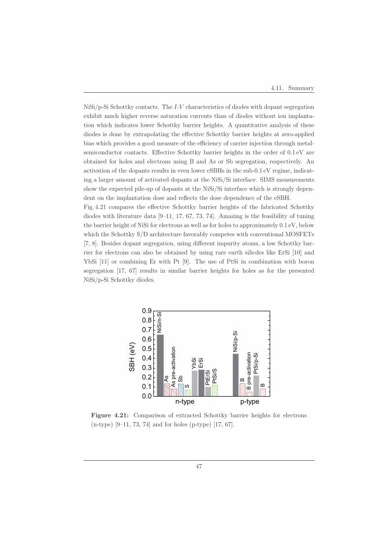
4.11. Summary
NiSi/p-Si Schottky contacts. The I-V characteristics of diodes with dopant segregation
exhibit much higher reverse saturation currents than of diodes without ion implanta-
tion which indicates lower Schottky barrier heights. A quantitative analysis of these
diodes is done by extrapolating the effective Schottky barrier heights at zero-applied
bias which provides a good measure of the efficiency of carrier injection through metal-
semiconductor contacts. Effective Schottky barrier heights in the order of 0.1 eV are
obtained for holes and electrons using B and As or Sb segregation, respectively. An
activation of the dopants results in even lower eSBHs in the sub-0.1 eV regime, indicat-
ing a larger amount of activated dopants at the NiSi/Si interface. SIMS measurements
show the expected pile-up of dopants at the NiSi/Si interface which is strongly depen-
dent on the implantation dose and reflects the dose dependence of the eSBH.
Fig. 4.21 compares the effective Schottky barrier heights of the fabricated Schottky
diodes with literature data [9–11, 17, 67, 73, 74]. Amazing is the feasibility of tuning
the barrier height of NiSi for electrons as well as for holes to approximately 0.1 eV, below
which the Schottky S/D architecture favorably competes with conventional MOSFETs
[7, 8]. Besides dopant segregation, using different impurity atoms, a low Schottky bar-
rier for electrons can also be obtained by using rare earth silicdes like ErSi [10] and
YbSi [11] or combining Er with Pt [9]. The use of PtSi in combination with boron
segregation [17, 67] results in similar barrier heights for holes as for the presented
NiSi/p-Si Schottky diodes.
0.00.10.20.30.40.50.60.70.80.9
PtS
i/SP
tErS
iErS
iY
bSi
S
p-type
Sb
As
pre-
activ
atio
nA
s
NiS
i/p-S
i
SB
H (e
V)
NiS
i/n-S
i
B p
re-a
ctiv
atio
nB
n-type
PtS
i/p-S
iB
Figure 4.21: Comparison of extracted Schottky barrier heights for electrons
(n-type) [9–11, 73, 74] and for holes (p-type) [17, 67].
47
Chapter 4. Schottky-Diodes
48
Chapter 5
Fabrication Process of
SB-MOSFETs
The mask layout and fabrication process of NiSi source/drain SB-MOSFETs on thin-
body SOI are described in the following sections. The emphasis is put on key process
steps with focus on the fabrication of short-channel devices.
5.1 Mask Design
Fig. 5.1 shows the mask layout for samples with a size of 22·22 mm2 which contains
the MOSFETs, different test structures and various control fields for processing. The
outer border lines with crosses in the edges which become successively smaller with each
process step deal as alignment markers for the optical lithography, whereas 15·15μm2
large squares are used as markers for electron-beam (e-beam) lithography. The two
large squares in the upper left corner which contain arrays of e-beam markers are
so-called pre-allocation markers (PAM) which simplify the adjustment of the samples
during e-beam writing. The two squares on the right side of the PAM fields allow a
control of each process step either by laser interferometry during dry etching or by
spectroscopic ellipsometry. The upper field contains the whole layer stack, including
the SOI substrate, the gate oxide and the gate stack, whereas the lower field is etched
down to the substrate. This is especially important for the SiO2 spacer etching since
in-situ laser interferometry during etching does not show any etch-stop signal on thin
SOI layers. The rectangle on the right side serves as control field and provides test
structures for TEM.
In the lower part each of the four areas, devided by alignment lines, contains 6 · 8 ·
49
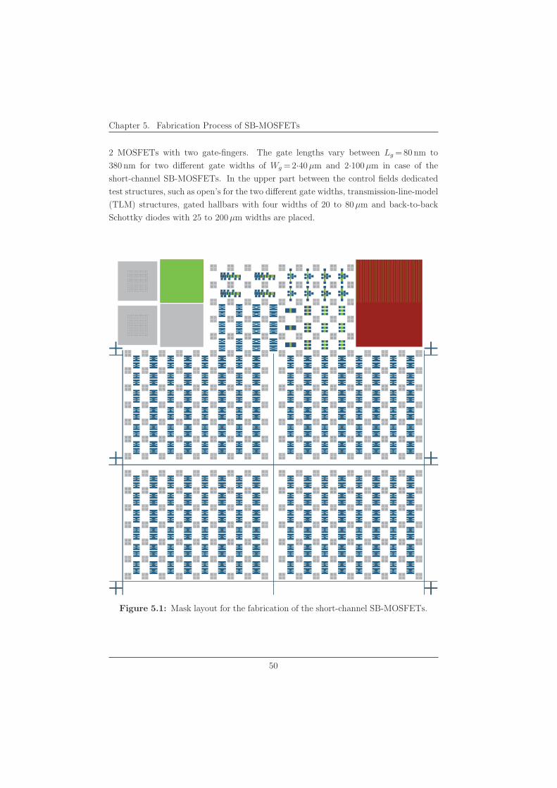
Chapter 5. Fabrication Process of SB-MOSFETs
2 MOSFETs with two gate-fingers. The gate lengths vary between Lg = 80 nm to
380 nm for two different gate widths of Wg = 2·40μm and 2·100μm in case of the
short-channel SB-MOSFETs. In the upper part between the control fields dedicated
test structures, such as open’s for the two different gate widths, transmission-line-model
(TLM) structures, gated hallbars with four widths of 20 to 80μm and back-to-back
Schottky diodes with 25 to 200μm widths are placed.
Figure 5.1: Mask layout for the fabrication of the short-channel SB-MOSFETs.
50
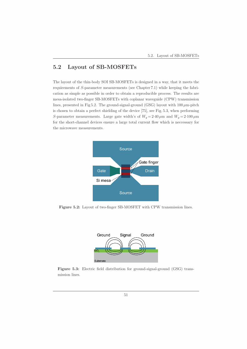
5.2. Layout of SB-MOSFETs
5.2 Layout of SB-MOSFETs
The layout of the thin-body SOI SB-MOSFETs is designed in a way, that it meets the
requirements of S-parameter measurements (see Chapter 7.1) while keeping the fabri-
cation as simple as possible in order to obtain a reproducible process. The results are
mesa-isolated two-finger SB-MOSFETs with coplanar waveguide (CPW) transmission
lines, presented in Fig 5.2. The ground-signal-ground (GSG) layout with 100μm-pitch
is chosen to obtain a perfect shielding of the device [75], see Fig. 5.3, when performing
S-parameter measurements. Large gate width’s of Wg = 2·40μm and Wg = 2·100μm
for the short-channel devices ensure a large total current flow which is neccessary for
the microwave measurements.
Figure 5.2: Layout of two-finger SB-MOSFET with CPW transmission lines.
Figure 5.3: Electric field distribution for ground-signal-ground (GSG) trans-
mission lines.
51
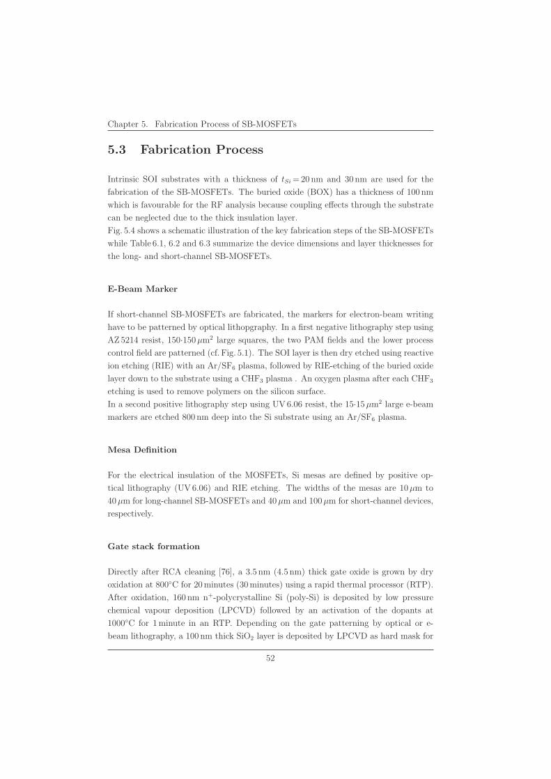
Chapter 5. Fabrication Process of SB-MOSFETs
5.3 Fabrication Process
Intrinsic SOI substrates with a thickness of tSi = 20 nm and 30 nm are used for the
fabrication of the SB-MOSFETs. The buried oxide (BOX) has a thickness of 100 nm
which is favourable for the RF analysis because coupling effects through the substrate
can be neglected due to the thick insulation layer.
Fig. 5.4 shows a schematic illustration of the key fabrication steps of the SB-MOSFETs
while Table 6.1, 6.2 and 6.3 summarize the device dimensions and layer thicknesses for
the long- and short-channel SB-MOSFETs.
E-Beam Marker
If short-channel SB-MOSFETs are fabricated, the markers for electron-beam writing
have to be patterned by optical lithopgraphy. In a first negative lithography step using
AZ 5214 resist, 150·150μm2 large squares, the two PAM fields and the lower process
control field are patterned (cf. Fig. 5.1). The SOI layer is then dry etched using reactive
ion etching (RIE) with an Ar/SF6 plasma, followed by RIE-etching of the buried oxide
layer down to the substrate using a CHF3 plasma . An oxygen plasma after each CHF3
etching is used to remove polymers on the silicon surface.
In a second positive lithography step using UV 6.06 resist, the 15·15μm2 large e-beam
markers are etched 800 nm deep into the Si substrate using an Ar/SF6 plasma.
Mesa Definition
For the electrical insulation of the MOSFETs, Si mesas are defined by positive op-
tical lithography (UV 6.06) and RIE etching. The widths of the mesas are 10μm to
40μm for long-channel SB-MOSFETs and 40μm and 100μm for short-channel devices,
respectively.
Gate stack formation
Directly after RCA cleaning [76], a 3.5 nm (4.5 nm) thick gate oxide is grown by dry
oxidation at 800◦C for 20 minutes (30 minutes) using a rapid thermal processor (RTP).
After oxidation, 160 nm n+-polycrystalline Si (poly-Si) is deposited by low pressure
chemical vapour deposition (LPCVD) followed by an activation of the dopants at
1000◦C for 1 minute in an RTP. Depending on the gate patterning by optical or e-
beam lithography, a 100 nm thick SiO2 layer is deposited by LPCVD as hard mask for
52
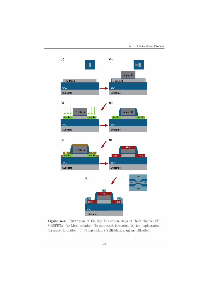
5.3. Fabrication Process
Figure 5.4: Illustration of the key fabrication steps of short channel SB-
MOSFETs. (a) Mesa isolation, (b) gate stack formation, (c) ion implantation,
(d) spacer formation, (e) Ni deposition, (f) silicidation, (g) metallization.
53
Chapter 5. Fabrication Process of SB-MOSFETs
gate-stack etching or the e-beam resist Hydrogensilsesquioxan (HSQ) is spinned on the
poly-Si.
In the case of long-channel devices, the 100 nm SiO2 on top of the poly-Si is patterned
by optical lithography, followed by reactive ion etching (CHF3). The poly-Si is then
structured by inductively coupled plasma etching (ICP-RIE), using the SiO2 on top
of the poly-Si as hard mask and the gate oxide as etch stop layer. In a first step, the
native oxide on top of the poly-Si is removed by pure HBr plasma. The high selectivity
between Si and SiO2 of the second step, an HBr : O2 plasma, permits an exact etch stop
and steep edges [77]. The resulting gate lengths range from Lg = 1.0μm to 4.0μm.
For short-channel SB-MOSFETs, e-beam lithography is used to define the gate stacks
with lengths from Lg = 80 nm to 380 nm, followed by ICP-etching, too. However, in
contrast to the SiO2 hard mask, the HSQ is completely etched during the ICP-etching
which avoids an additional step to open the gate contact windows and facilitates a
partial silicidation of the gate stack. Fig. 5.5 shows a scanning electron microscopy
(SEM) image of a straigth gate finger (Lg = 180 nm) with its steep edges.
Figure 5.5: SEM image (60◦ tilted) of the Si mesa of a SB-MOSFET on thin-
body SOI (tSi = 30 nm) with a 3.5 nm gate oxide and a 160 nm thick n+-poly-Si
gate; the channel length is 180 nm.
Ion Implantation
A wet etching step using 1% HF removes the gate oxide at S/D in order to implant
directly into the SOI layer. For SB-MOSFETs with dopant segregation, either B+ at
an energy of 1.5 keV or As+ at an energy of 5 keV are implanted under a tilt angle
of 0◦, leading to an implantation depth of approximately 8 nm in both cases. For the
B+ implantation, different doses of 5·1014 B/cm2, 1·1015 B/cm2 and 3·1015 B/cm2 are
chosen. For the As+ implantation doses ranging from 5·1013 As/cm2 to 6·1015 As/cm2
are used.
54
5.3. Fabrication Process
Gate Spacer Formation
After implantation tetra-ethyl-ortho-silicate (TEOS) is deposited by LPCVD which
ensures a conformal deposition of SiO2 and a perfect coverage of the edges. During
the following anisotropic dry etching by RIE in a CHF3 plasma, SiO2 gate spacers are
formed. This step is very critical since the SiO2 has to be etched away completely
while the thin SOI layer serves as etch stop layer. Therefore, a very good selectivity
between SiO2 and Si is mandatory to prevent a loss of the highly doped silicon S/D
regions. Whereas the long-channel SB-MOSFETs and the first batch of the short-
channel devices are etched with a poor selectivity, a drastically improved CHF3 process
is developed and used for the short-channel devices with different As+ implantation
doses (see Chapter 7.7). Here, a selectivity better than 10 : 1 at an etch rate of
60 nm/min results in improved device characteristics.
Gate Contact Window Opening
Negative Optical lithography (AZ 5206) is used to pattern the gate contact windows in
case of long-channel SB-MOSFETs. The SiO2 hard mask on top of the poly-Si is then
etched by RIE.
Silicidation
The samples are then cleaned using SPM (H2SO4 : H2O2 = 4 : 1), and directly after an
HF-dip (1%) for 30 s Ni is deposited by electron-beam evaporation. The required Ni
thickness strongly depends on tSi. For the subsequent silicidation step, a temperature
of 450 ◦C and a time of 30 seconds are chosen in order to facilitate dopant segregation
and the encroachment of NiSi into the channel region as displayed in Fig. 5.6 for a
80 nm short-channel MOSFET. The unreacted Ni is selectively wet etched using SPM.
Whereas Fig. 5.6(a) shows a standard SEM image, the bright-field scanning transmis-
sion electron microscopy (STEM) image, Fig. 5.6(b), shows a Z-contrast, where heavy
atoms like Pt and Ni appear in dark and light atoms in bright colors. The different
contrasts of the Pt layers are a result of two deposition techniques.
55
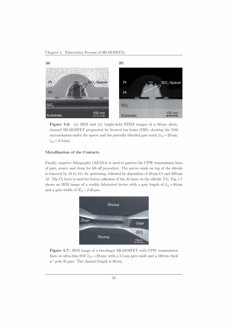
Chapter 5. Fabrication Process of SB-MOSFETs
(a) (b)
Substrate
SiO2
Pt
Pt SiO2-SpacerNiSi
NiSi NiSi
Substrate
SiO2
Pt
Pt SiO2-SpacerNiSi
NiSi NiSi
100 nm 100 nm
Figure 5.6: (a) SEM and (b) bright-field STEM images of a 80 nm short-
channel SB-MOSFET preparated by focused ion beam (FIB), showing the NiSi
encroachment under the spacer and the partially silicided gate stack (tSi = 20 nm,
tox = 4.5 nm).
Metallization of the Contacts
Finally, negative lithography (AZ 5214) is used to pattern the CPW transmission lines
of gate, source and drain for lift-off procedure. The native oxide on top of the silicide
is removed by 10 to 15 s Ar sputtering, followed by deposition of 20 nm Cr and 200 nm
Al. The Cr layer is used for better adhesion of the Al layer on the silicide [71]. Fig. 5.7
shows an SEM image of a readily fabricated device with a gate length of Lg = 80 nm
and a gate-width of Wg = 2·40μm.
Figure 5.7: SEM image of a two-finger SB-MOSFET with CPW transmission
lines on ultra-thin SOI (tSi = 20 nm) with a 3.5 nm gate oxide and a 160 nm thick
n+-poly-Si gate. The channel length is 80 nm.
56
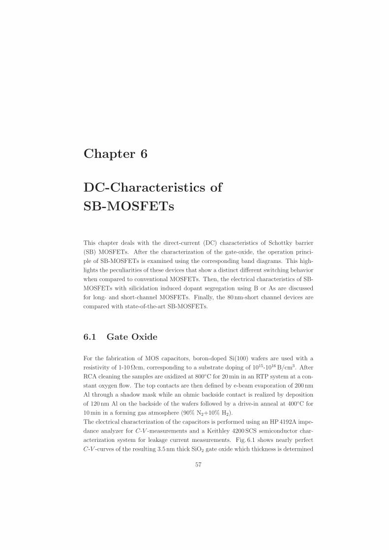
Chapter 6
DC-Characteristics of
SB-MOSFETs
This chapter deals with the direct-current (DC) characteristics of Schottky barrier
(SB) MOSFETs. After the characterization of the gate-oxide, the operation princi-
ple of SB-MOSFETs is examined using the corresponding band diagrams. This high-
lights the peculiarities of these devices that show a distinct different switching behavior
when compared to conventional MOSFETs. Then, the electrical characteristics of SB-
MOSFETs with silicidation induced dopant segregation using B or As are discussed
for long- and short-channel MOSFETs. Finally, the 80 nm-short channel devices are
compared with state-of-the-art SB-MOSFETs.
6.1 Gate Oxide
For the fabrication of MOS capacitors, boron-doped Si(100) wafers are used with a
resistivity of 1-10 Ωcm, corresponding to a substrate doping of 1015-1016 B/cm3. After
RCA cleaning the samples are oxidized at 800◦C for 20 min in an RTP system at a con-
stant oxygen flow. The top contacts are then defined by e-beam evaporation of 200 nm
Al through a shadow mask while an ohmic backside contact is realized by deposition
of 120 nm Al on the backside of the wafers followed by a drive-in anneal at 400◦C for
10 min in a forming gas atmosphere (90% N2+10% H2).
The electrical characterization of the capacitors is performed using an HP 4192A impe-
dance analyzer for C-V -measurements and a Keithley 4200 SCS semiconductor char-
acterization system for leakage current measurements. Fig. 6.1 shows nearly perfect
C-V -curves of the resulting 3.5 nm thick SiO2 gate oxide which thickness is determined
57
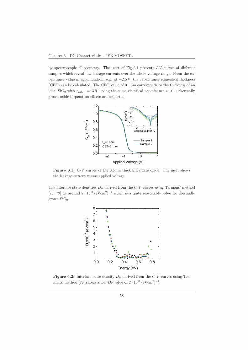
Chapter 6. DC-Characteristics of SB-MOSFETs
by spectroscopic ellipsometry. The inset of Fig. 6.1 presents I-V -curves of different
samples which reveal low leakage currents over the whole voltage range. From the ca-
pacitance value in accumulation, e.g. at −2.5 V, the capacitance equivalent thickness
(CET) can be calculated. The CET value of 3.1 nm corresponds to the thickness of an
ideal SiO2 with εSiO2 = 3.9 having the same electrical capacitance as this thermally
grown oxide if quantum effects are neglected.
-2 -1 010-12
10-10
10-8
10-6
10-4
-2 -1 0 10.0
0.2
0.4
0.6
0.8
1.0
1.2
������
� �
Applied Voltage (V)
Sample 1 Sample 2tox=3.5nm
CET=3.1nm
���� ���
� �
Applied Voltage (V)
Figure 6.1: C-V curves of the 3.5 nm thick SiO2 gate oxide. The inset shows
the leakage current versus applied voltage.
The interface state densities Dit derived from the C-V curves using Termans’ method
[78, 79] lie around 2 · 1011 (eVcm2)−1 which is a quite reasonable value for thermally
grown SiO2.
0.0 0.2 0.4 0.6 0.8
1
2
3
4
5
6
7
8
Ditx1
012 (e
Vcm
2 )-1
Energy (eV)
Figure 6.2: Interface state density Dit derived from the C-V curves using Ter-
mans’ method [78] shows a low Dit value of 2 · 1011 (eVcm2)−1.
58
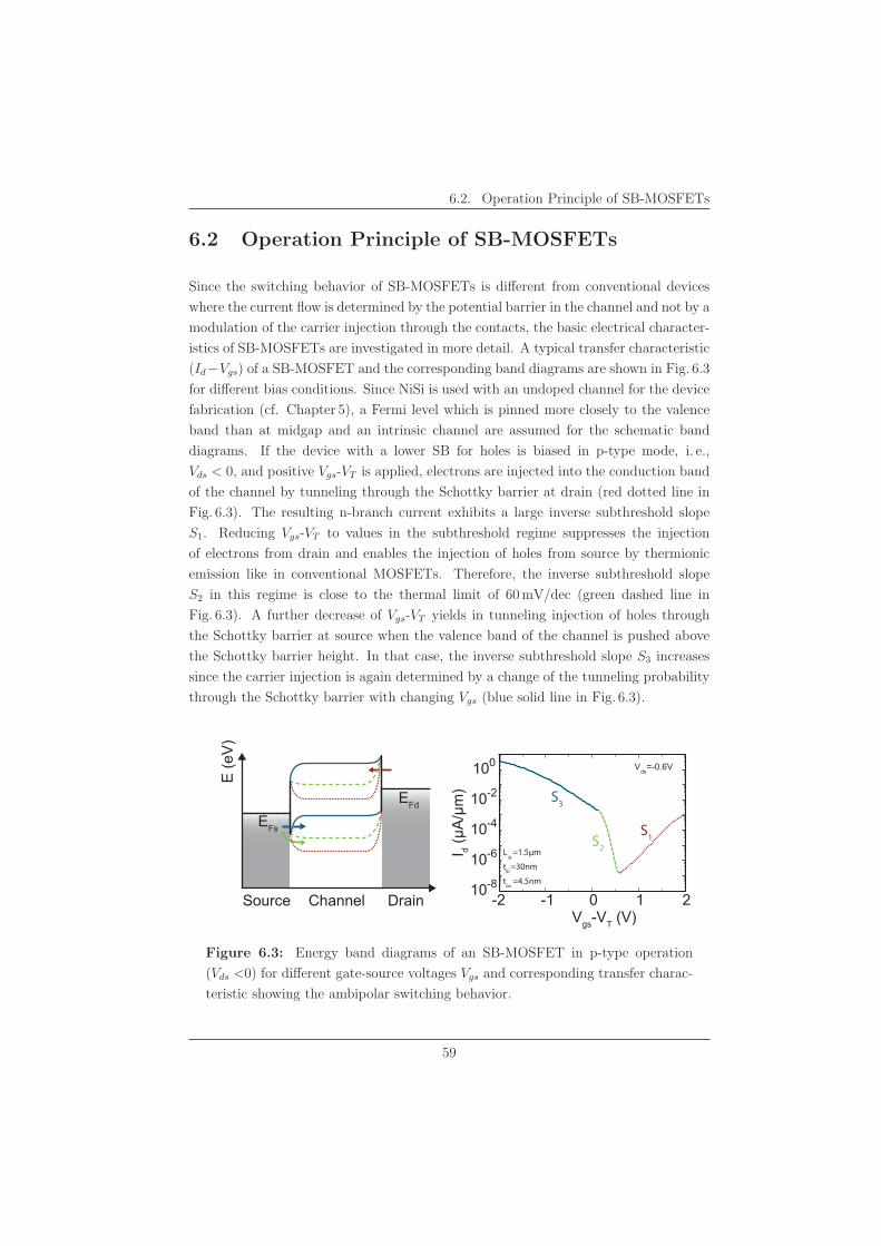
6.2. Operation Principle of SB-MOSFETs
6.2 Operation Principle of SB-MOSFETs
Since the switching behavior of SB-MOSFETs is different from conventional devices
where the current flow is determined by the potential barrier in the channel and not by a
modulation of the carrier injection through the contacts, the basic electrical character-
istics of SB-MOSFETs are investigated in more detail. A typical transfer characteristic
(Id−Vgs) of a SB-MOSFET and the corresponding band diagrams are shown in Fig. 6.3
for different bias conditions. Since NiSi is used with an undoped channel for the device
fabrication (cf. Chapter 5), a Fermi level which is pinned more closely to the valence
band than at midgap and an intrinsic channel are assumed for the schematic band
diagrams. If the device with a lower SB for holes is biased in p-type mode, i. e.,
Vds < 0, and positive Vgs-VT is applied, electrons are injected into the conduction band
of the channel by tunneling through the Schottky barrier at drain (red dotted line in
Fig. 6.3). The resulting n-branch current exhibits a large inverse subthreshold slope
S1. Reducing Vgs-VT to values in the subthreshold regime suppresses the injection
of electrons from drain and enables the injection of holes from source by thermionic
emission like in conventional MOSFETs. Therefore, the inverse subthreshold slope
S2 in this regime is close to the thermal limit of 60 mV/dec (green dashed line in
Fig. 6.3). A further decrease of Vgs-VT yields in tunneling injection of holes through
the Schottky barrier at source when the valence band of the channel is pushed above
the Schottky barrier height. In that case, the inverse subthreshold slope S3 increases
since the carrier injection is again determined by a change of the tunneling probability
through the Schottky barrier with changing Vgs (blue solid line in Fig. 6.3).
Source Channel Drain
E (e
V)
EFd
EFs
-2 -1 0 1 210-8
10-6
10-4
10-2
100
Lg
=1.5μm
tSi
=30nm
tox
=4.5nm
Id (
μA/μ
m)
Vgs-VT (V)
Vds
=-0.6V
S3
S2
S1
Figure 6.3: Energy band diagrams of an SB-MOSFET in p-type operation
(Vds <0) for different gate-source voltages Vgs and corresponding transfer charac-
teristic showing the ambipolar switching behavior.
59
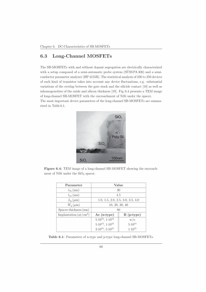
Chapter 6. DC-Characteristics of SB-MOSFETs
6.3 Long-Channel MOSFETs
The SB-MOSFETs with and without dopant segregation are electrically characterized
with a setup composed of a semi-automatic probe system (SUSS PA 300) and a semi-
conductor parameter analyzer (HP 4155B). The statistical analysis of 230 to 250 devices
of each kind of transistor takes into account any device fluctuations, e.g. substantial
variations of the overlap between the gate stack and the silicide contact [18] as well as
inhomogeneities of the oxide and silicon thickness [19]. Fig. 6.4 presents a TEM image
of long-channel SB-MOSFET with the encroachment of NiSi under the spacer.
The most important device parameters of the long-channel SB-MOSFETs are summa-
rized in Table 6.1.
Figure 6.4: TEM image of a long-channel SB-MOSFET showing the encroach-
ment of NiSi under the SiO2 spacer.
Parameter Value
tSi (nm) 30
tox (nm) 4.5
Lg (μm) 1.0, 1.5, 2.0, 2.5, 3.0, 3.5, 4.0
Wg (μm) 10, 20, 30, 40
Spacer-thickness (nm) 80
Implantation (at/cm2) As (n-type) B (p-type)
5·1013, 1·1014 w/o
5·1014, 1·1015 5·1014
3·1015, 5·1015 1·1015
Table 6.1: Parameters of n-type and p-type long-channel SB-MOSFETs.
60
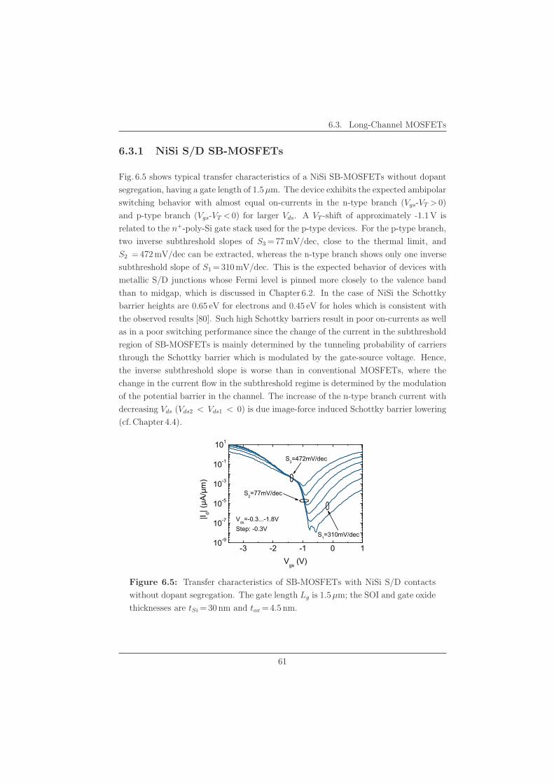
6.3. Long-Channel MOSFETs
6.3.1 NiSi S/D SB-MOSFETs
Fig. 6.5 shows typical transfer characteristics of a NiSi SB-MOSFETs without dopant
segregation, having a gate length of 1.5μm. The device exhibits the expected ambipolar
switching behavior with almost equal on-currents in the n-type branch (Vgs-VT > 0)
and p-type branch (Vgs-VT < 0) for larger Vds. A VT -shift of approximately -1.1 V is
related to the n+-poly-Si gate stack used for the p-type devices. For the p-type branch,
two inverse subthreshold slopes of S3 = 77 mV/dec, close to the thermal limit, and
S2 = 472 mV/dec can be extracted, whereas the n-type branch shows only one inverse
subthreshold slope of S1 = 310 mV/dec. This is the expected behavior of devices with
metallic S/D junctions whose Fermi level is pinned more closely to the valence band
than to midgap, which is discussed in Chapter 6.2. In the case of NiSi the Schottky
barrier heights are 0.65 eV for electrons and 0.45 eV for holes which is consistent with
the observed results [80]. Such high Schottky barriers result in poor on-currents as well
as in a poor switching performance since the change of the current in the subthreshold
region of SB-MOSFETs is mainly determined by the tunneling probability of carriers
through the Schottky barrier which is modulated by the gate-source voltage. Hence,
the inverse subthreshold slope is worse than in conventional MOSFETs, where the
change in the current flow in the subthreshold regime is determined by the modulation
of the potential barrier in the channel. The increase of the n-type branch current with
decreasing Vds (Vds2 < Vds1 < 0) is due image-force induced Schottky barrier lowering
(cf. Chapter 4.4).
-3 -2 -1 0 110-9
10-7
10-5
10-3
10-1
101
S1=310mV/dec
S2=77mV/dec
!� "!���
����
Vgs (V)
Vds=-0.3...-1.8VStep: -0.3V
S3=472mV/dec
Figure 6.5: Transfer characteristics of SB-MOSFETs with NiSi S/D contacts
without dopant segregation. The gate length Lg is 1.5μm; the SOI and gate oxide
thicknesses are tSi = 30 nm and tox = 4.5 nm.
61
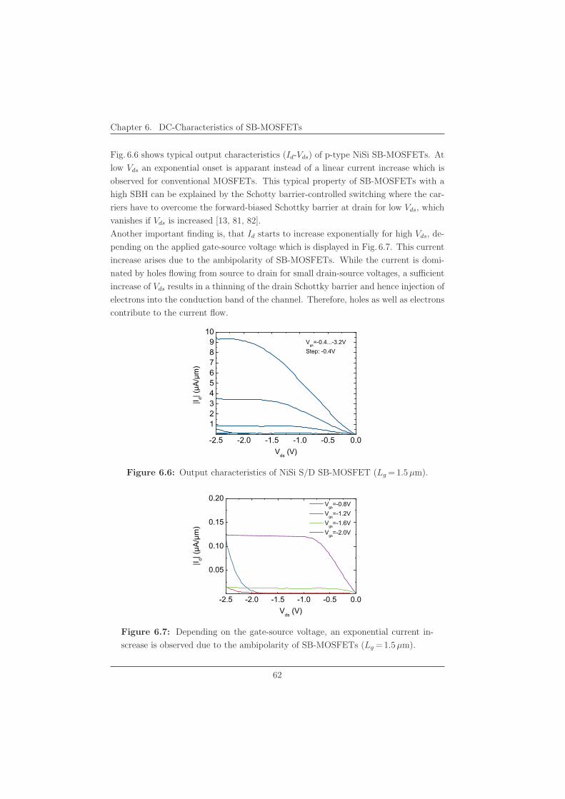
Chapter 6. DC-Characteristics of SB-MOSFETs
Fig. 6.6 shows typical output characteristics (Id-Vds) of p-type NiSi SB-MOSFETs. At
low Vds an exponential onset is apparant instead of a linear current increase which is
observed for conventional MOSFETs. This typical property of SB-MOSFETs with a
high SBH can be explained by the Schotty barrier-controlled switching where the car-
riers have to overcome the forward-biased Schottky barrier at drain for low Vds, which
vanishes if Vds is increased [13, 81, 82].
Another important finding is, that Id starts to increase exponentially for high Vds, de-
pending on the applied gate-source voltage which is displayed in Fig. 6.7. This current
increase arises due to the ambipolarity of SB-MOSFETs. While the current is domi-
nated by holes flowing from source to drain for small drain-source voltages, a sufficient
increase of Vds results in a thinning of the drain Schottky barrier and hence injection of
electrons into the conduction band of the channel. Therefore, holes as well as electrons
contribute to the current flow.
-2.5 -2.0 -1.5 -1.0 -0.5 0.0
123456789
10
�� ������
��
Vds (V)
Vgs
=-0.4...-3.2VStep: -0.4V
Figure 6.6: Output characteristics of NiSi S/D SB-MOSFET (Lg = 1.5μm).
-2.5 -2.0 -1.5 -1.0 -0.5 0.0
0.05
0.10
0.15
0.20
|I d| (μA
/μm
)
Vds (V)
Vgs=-0.8V Vgs=-1.2V Vgs=-1.6V Vgs=-2.0V
Figure 6.7: Depending on the gate-source voltage, an exponential current in-
screase is observed due to the ambipolarity of SB-MOSFETs (Lg = 1.5μm).
62
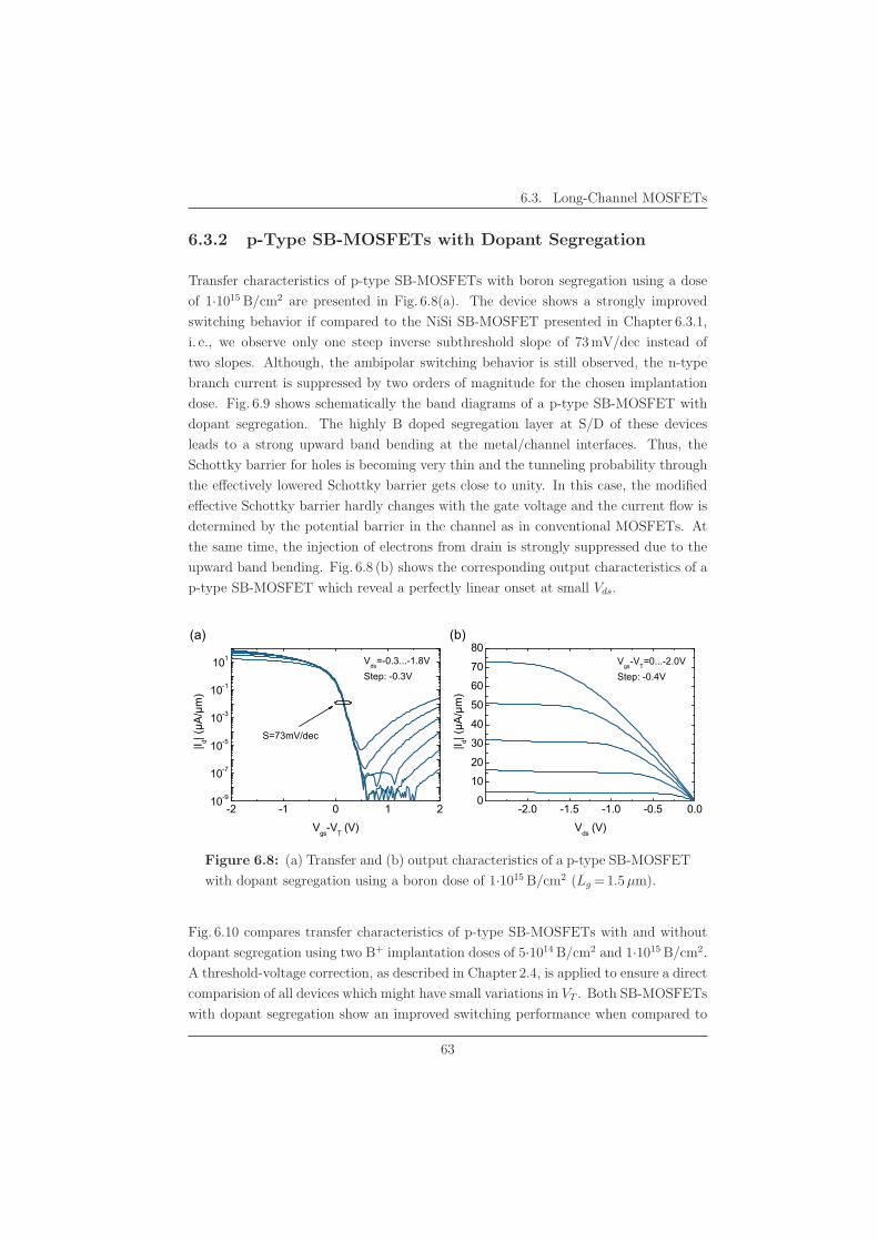
6.3. Long-Channel MOSFETs
6.3.2 p-Type SB-MOSFETs with Dopant Segregation
Transfer characteristics of p-type SB-MOSFETs with boron segregation using a dose
of 1·1015 B/cm2 are presented in Fig. 6.8(a). The device shows a strongly improved
switching behavior if compared to the NiSi SB-MOSFET presented in Chapter 6.3.1,
i. e., we observe only one steep inverse subthreshold slope of 73 mV/dec instead of
two slopes. Although, the ambipolar switching behavior is still observed, the n-type
branch current is suppressed by two orders of magnitude for the chosen implantation
dose. Fig. 6.9 shows schematically the band diagrams of a p-type SB-MOSFET with
dopant segregation. The highly B doped segregation layer at S/D of these devices
leads to a strong upward band bending at the metal/channel interfaces. Thus, the
Schottky barrier for holes is becoming very thin and the tunneling probability through
the effectively lowered Schottky barrier gets close to unity. In this case, the modified
effective Schottky barrier hardly changes with the gate voltage and the current flow is
determined by the potential barrier in the channel as in conventional MOSFETs. At
the same time, the injection of electrons from drain is strongly suppressed due to the
upward band bending. Fig. 6.8 (b) shows the corresponding output characteristics of a
p-type SB-MOSFET which reveal a perfectly linear onset at small Vds.
-2 -1 0 1 210-9
10-7
10-5
10-3
10-1
101
-2.0 -1.5 -1.0 -0.5 0.00
10
20
30
40
50
60
70
80(b)
!� "!���
����
Vgs
-VT (V)
Vds=-0.3...-1.8VStep: -0.3V
S=73mV/dec
(a)
!� "!���
����
Vds
(V)
Vgs-VT=0...-2.0VStep: -0.4V
Figure 6.8: (a) Transfer and (b) output characteristics of a p-type SB-MOSFET
with dopant segregation using a boron dose of 1·1015 B/cm2 (Lg = 1.5μm).
Fig. 6.10 compares transfer characteristics of p-type SB-MOSFETs with and without
dopant segregation using two B+ implantation doses of 5·1014 B/cm2 and 1·1015 B/cm2.
A threshold-voltage correction, as described in Chapter 2.4, is applied to ensure a direct
comparision of all devices which might have small variations in VT . Both SB-MOSFETs
with dopant segregation show an improved switching performance when compared to
63
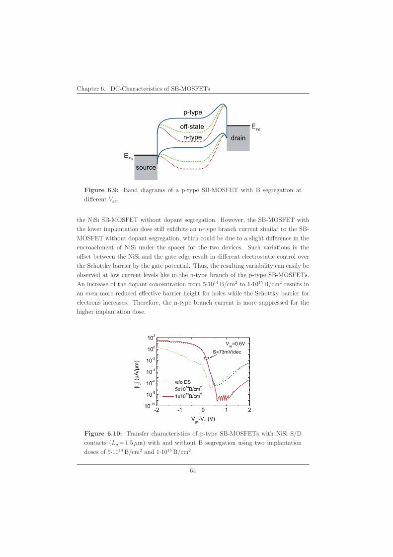
Chapter 6. DC-Characteristics of SB-MOSFETs
EFs
source
drain
EFd
p-type
n-typeoff-state
Figure 6.9: Band diagrams of a p-type SB-MOSFET with B segregation at
different Vgs.
the NiSi SB-MOSFET without dopant segregation. However, the SB-MOSFET with
the lower implantation dose still exhibits an n-type branch current similar to the SB-
MOSFET without dopant segregation, which could be due to a slight difference in the
encroachment of NiSi under the spacer for the two devices. Such variations in the
offset between the NiSi and the gate edge result in different electrostatic control over
the Schottky barrier by the gate potential. Thus, the resulting variability can easily be
observed at low current levels like in the n-type branch of the p-type SB-MOSFETs.
An increase of the dopant concentration from 5·1014 B/cm2 to 1·1015 B/cm2 results in
an even more reduced effective barrier height for holes while the Schottky barrier for
electrons increases. Therefore, the n-type branch current is more suppressed for the
higher implantation dose.
-2 -1 0 1 210-10
10-8
10-6
10-4
10-2
100
102
�� ������
��
Vgs-VT (V)
w/o DS 5x10¹⁴B/cm2
1x10¹⁵B/cm2
Vds=0.6V
S=73mV/dec
Figure 6.10: Transfer characteristics of p-type SB-MOSFETs with NiSi S/D
contacts (Lg = 1.5μm) with and without B segregation using two implantation
doses of 5·1014 B/cm2 and 1·1015 B/cm2.
64
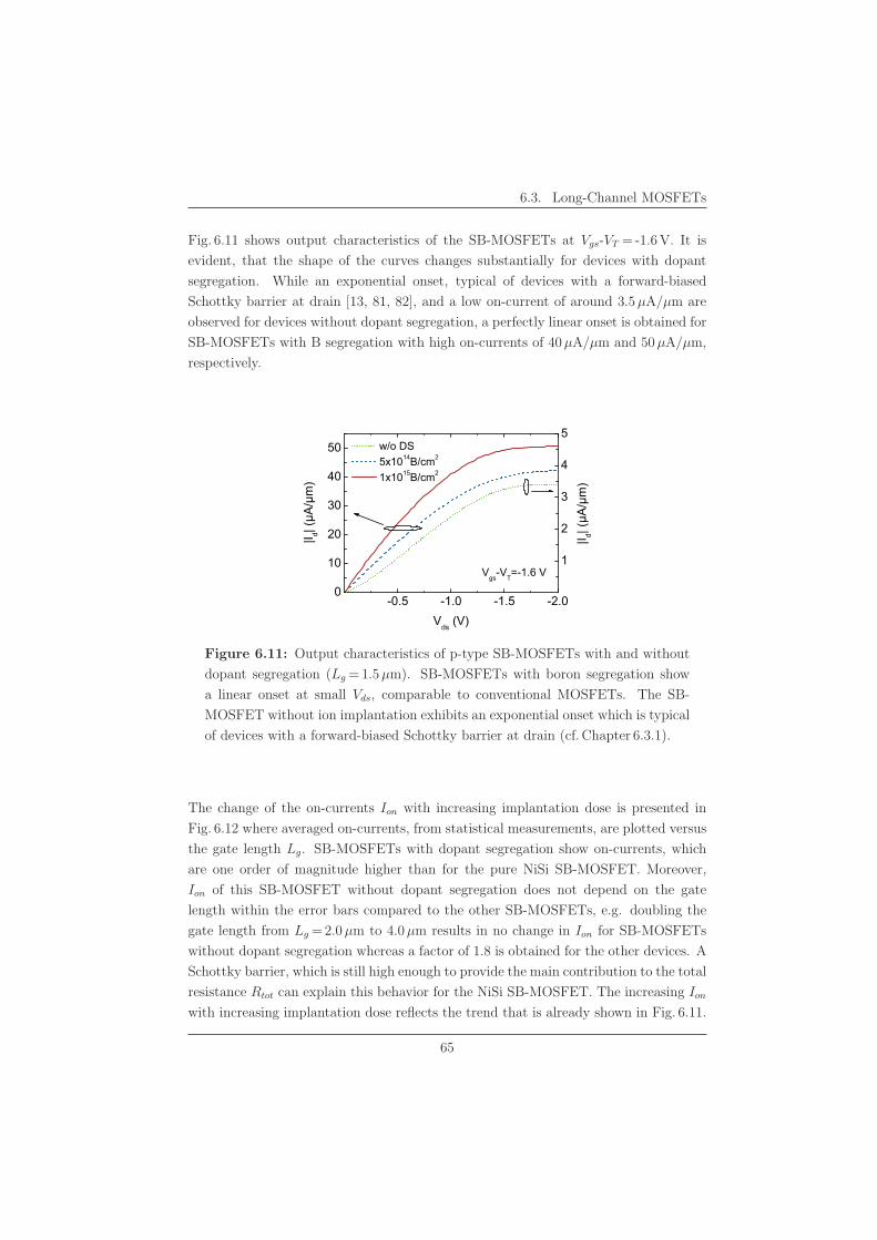
6.3. Long-Channel MOSFETs
Fig. 6.11 shows output characteristics of the SB-MOSFETs at Vgs-VT = -1.6 V. It is
evident, that the shape of the curves changes substantially for devices with dopant
segregation. While an exponential onset, typical of devices with a forward-biased
Schottky barrier at drain [13, 81, 82], and a low on-current of around 3.5 μA/μm are
observed for devices without dopant segregation, a perfectly linear onset is obtained for
SB-MOSFETs with B segregation with high on-currents of 40μA/μm and 50μA/μm,
respectively.
-0.5 -1.0 -1.5 -2.00
10
20
30
40
50
Vgs-VT=-1.6 V
�� ������
��
Vds (V)
w/o DS 5x10¹⁴B/cm2
1x10¹⁵B/cm2
1
2
3
4
5
�����������
Figure 6.11: Output characteristics of p-type SB-MOSFETs with and without
dopant segregation (Lg = 1.5μm). SB-MOSFETs with boron segregation show
a linear onset at small Vds, comparable to conventional MOSFETs. The SB-
MOSFET without ion implantation exhibits an exponential onset which is typical
of devices with a forward-biased Schottky barrier at drain (cf. Chapter 6.3.1).
The change of the on-currents Ion with increasing implantation dose is presented in
Fig. 6.12 where averaged on-currents, from statistical measurements, are plotted versus
the gate length Lg. SB-MOSFETs with dopant segregation show on-currents, which
are one order of magnitude higher than for the pure NiSi SB-MOSFET. Moreover,
Ion of this SB-MOSFET without dopant segregation does not depend on the gate
length within the error bars compared to the other SB-MOSFETs, e.g. doubling the
gate length from Lg = 2.0μm to 4.0μm results in no change in Ion for SB-MOSFETs
without dopant segregation whereas a factor of 1.8 is obtained for the other devices. A
Schottky barrier, which is still high enough to provide the main contribution to the total
resistance Rtot can explain this behavior for the NiSi SB-MOSFET. The increasing Ion
with increasing implantation dose reflects the trend that is already shown in Fig. 6.11.
65
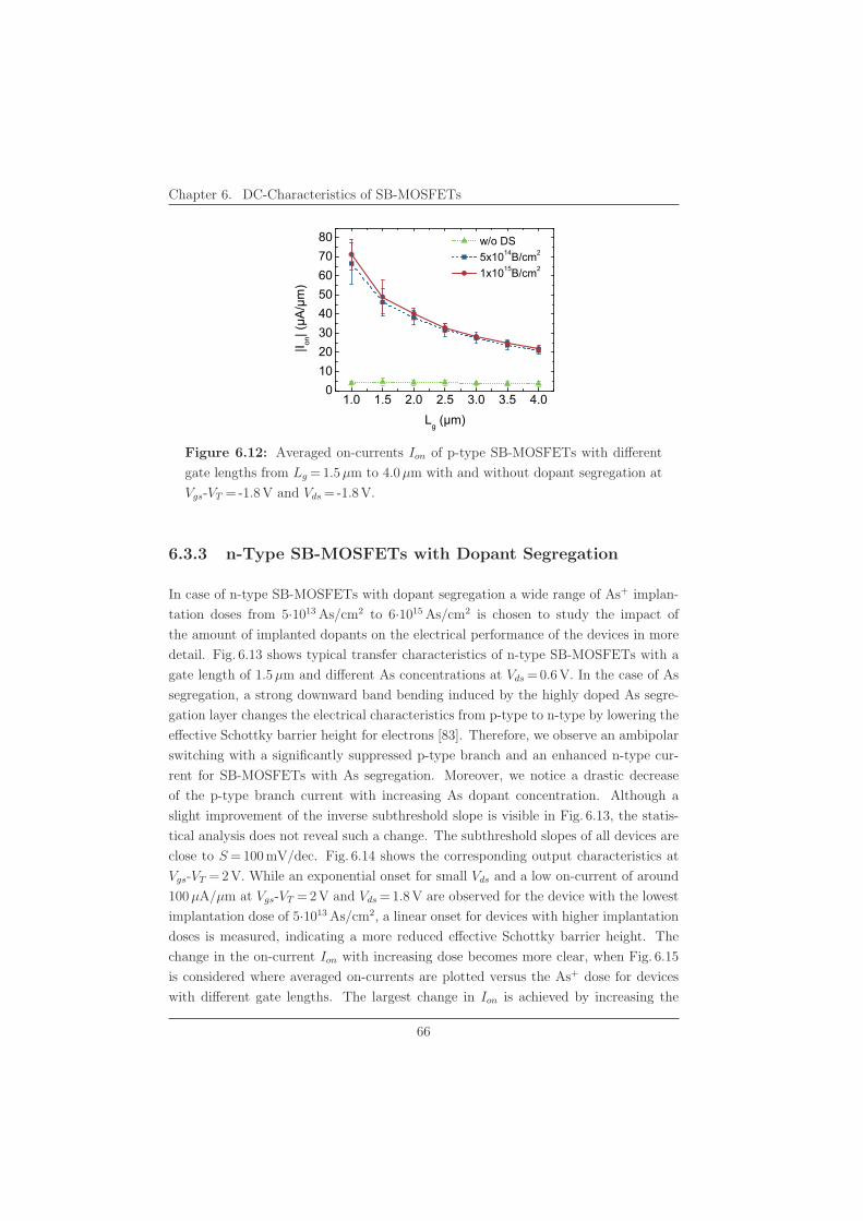
Chapter 6. DC-Characteristics of SB-MOSFETs
1.0 1.5 2.0 2.5 3.0 3.5 4.00
1020304050607080
'$ #�'��()�(��
��� ����
� �� � � ����������
� ����������
Figure 6.12: Averaged on-currents Ion of p-type SB-MOSFETs with different
gate lengths from Lg = 1.5μm to 4.0μm with and without dopant segregation at
Vgs-VT = -1.8 V and Vds = -1.8 V.
6.3.3 n-Type SB-MOSFETs with Dopant Segregation
In case of n-type SB-MOSFETs with dopant segregation a wide range of As+ implan-
tation doses from 5·1013 As/cm2 to 6·1015 As/cm2 is chosen to study the impact of
the amount of implanted dopants on the electrical performance of the devices in more
detail. Fig. 6.13 shows typical transfer characteristics of n-type SB-MOSFETs with a
gate length of 1.5μm and different As concentrations at Vds = 0.6 V. In the case of As
segregation, a strong downward band bending induced by the highly doped As segre-
gation layer changes the electrical characteristics from p-type to n-type by lowering the
effective Schottky barrier height for electrons [83]. Therefore, we observe an ambipolar
switching with a significantly suppressed p-type branch and an enhanced n-type cur-
rent for SB-MOSFETs with As segregation. Moreover, we notice a drastic decrease
of the p-type branch current with increasing As dopant concentration. Although a
slight improvement of the inverse subthreshold slope is visible in Fig. 6.13, the statis-
tical analysis does not reveal such a change. The subthreshold slopes of all devices are
close to S = 100 mV/dec. Fig. 6.14 shows the corresponding output characteristics at
Vgs-VT = 2 V. While an exponential onset for small Vds and a low on-current of around
100 μA/μm at Vgs-VT = 2 V and Vds = 1.8 V are observed for the device with the lowest
implantation dose of 5·1013 As/cm2, a linear onset for devices with higher implantation
doses is measured, indicating a more reduced effective Schottky barrier height. The
change in the on-current Ion with increasing dose becomes more clear, when Fig. 6.15
is considered where averaged on-currents are plotted versus the As+ dose for devices
with different gate lengths. The largest change in Ion is achieved by increasing the
66
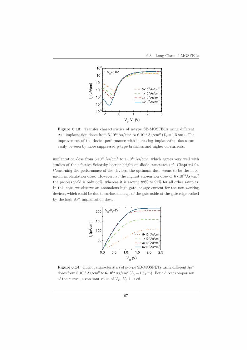
6.3. Long-Channel MOSFETs
-1 0 1 2 310-9
10-7
10-5
10-3
10-1
101
103
5x10¹³As/cm2
1x10¹⁴As/cm2
3x10¹⁵As/cm2
6x10¹⁵As/cm2
� "�������
Vgs-VT (V)
Vds=0.6V
Figure 6.13: Transfer characteristics of n-type SB-MOSFETs using different
As+ implantation doses from 5·1013 As/cm2 to 6·1015 As/cm2 (Lg = 1.5μm). The
improvement of the device performance with increasing implantation doses can
easily be seen by more suppressed p-type branches and higher on-currents.
implantation dose from 5·1013 As/cm2 to 1·1014 As/cm2, which agrees very well with
studies of the effective Schottky barrier height on diode structures (cf. Chapter 4.9).
Concerning the performance of the devices, the optimum dose seems to be the max-
imum implantation dose. However, at the highest chosen ion dose of 6 · 1015As/cm2
the process yield is only 55%, whereas it is around 89% to 97% for all other samples.
In this case, we observe an anomalous high gate leakage current for the non-working
devices, which could be due to surface damage of the gate oxide at the gate edge evoked
by the high As+ implantation dose.
0.0 0.5 1.0 1.5 2.0 2.5
50
100
150
200 Vgs-VT=2V
� �������
Vds (V)
5x10¹³As/cm2
1x10¹⁴As/cm2
3x10¹⁵As/cm2
6x10¹⁵As/cm2
Figure 6.14: Output characteristics of n-type SB-MOSFETs using different As+
doses from 5·1013 As/cm2 to 6·1015 As/cm2 (Lg = 1.5μm). For a direct comparison
of the curves, a constant value of Vgs -VT is used.
67
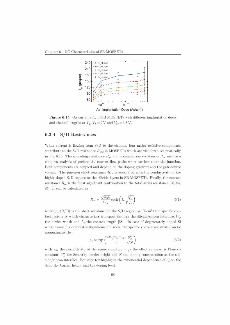
Chapter 6. DC-Characteristics of SB-MOSFETs
1014 1015
60
90
120
150
180
210
240
� ��������
���� ������ ��� ����� ��������
� ���������� ��������� ��������� ��������� ��������
Figure 6.15: On-currents Ion of SB-MOSFETs with different implantation doses
and channel lengths at Vgs-VT = 2 V and Vds = 1.8 V.
6.3.4 S/D Resistances
When current is flowing from S/D to the channel, four major resistive components
contribute to the S/D resistance Rs/d in MOSFETs which are visualized schematically
in Fig. 6.16. The spreading resistance Rsp and accumulation resistances Rac involve a
complex analysis of preferential current flow paths when carriers enter the junction.
Both components are coupled and depend on the doping gradient and the gate-source
voltage. The junction sheet resistance Rsh is associated with the conductivity of the
highly doped S/D regions or the silicide layers in SB-MOSFETs. Finally, the contact
resistance Rco is the most significant contribution to the total series resistance [58, 84,
85]. It can be calculated as
Rco =
√ρsρc
Wg
coth
(Lc
√ρs
ρc
)(6.1)
where ρs (Ω/�) is the sheet resistance of the S/D region, ρc (Ωcm2) the specific con-
tact resistivity which characterizes transport through the silicide/silicon interface, Wg
the device width and Lc the contact length [58]. In case of degenerately doped Si
where tunneling dominates thermionic emission, the specific contact resistivity can be
approximated by:
ρc ≈ exp
(4π
√εSimeff
h
Φ0B√N
)(6.2)
with εSi the permittivity of the semiconductor, meff the effective mass, h Planck’s
constant, Φ0B the Schottky barrier height and N the doping concentration at the sili-
cide/silicon interface. Equation 6.2 highlights the exponential dependence of ρc on the
Schottky barrier height and the doping level.
68
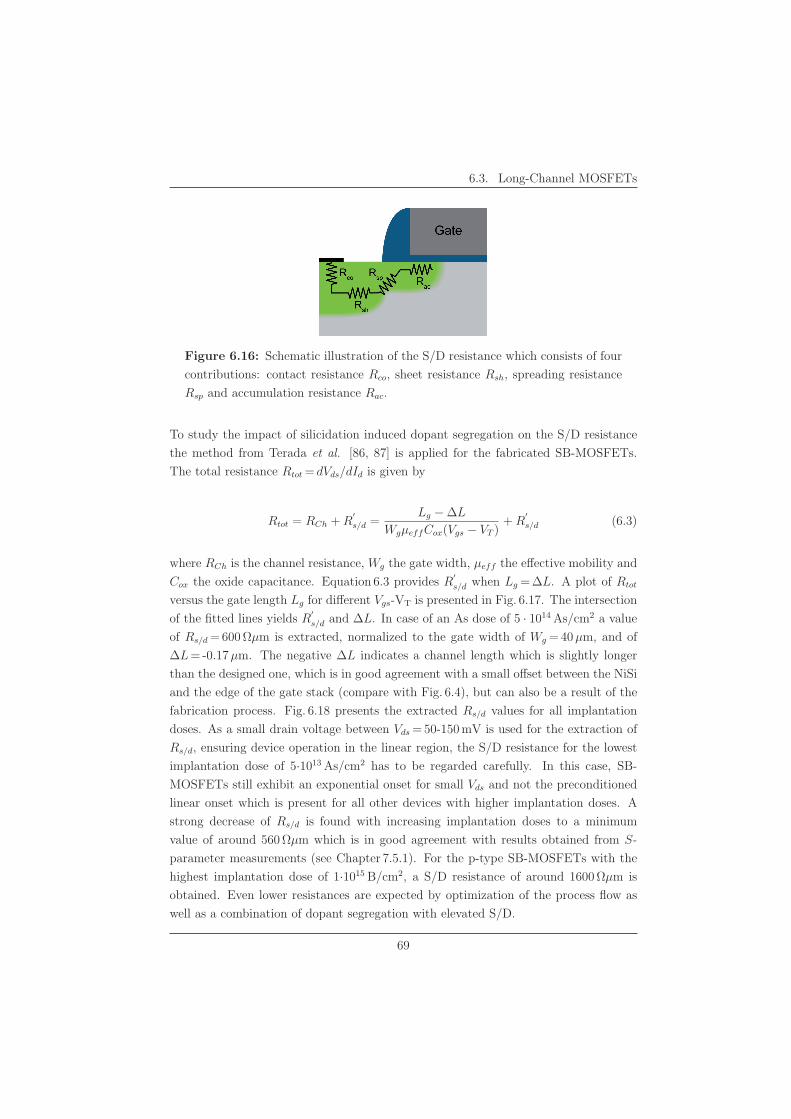
6.3. Long-Channel MOSFETs
Figure 6.16: Schematic illustration of the S/D resistance which consists of four
contributions: contact resistance Rco, sheet resistance Rsh, spreading resistance
Rsp and accumulation resistance Rac.
To study the impact of silicidation induced dopant segregation on the S/D resistance
the method from Terada et al. [86, 87] is applied for the fabricated SB-MOSFETs.
The total resistance Rtot = dVds/dId is given by
Rtot = RCh + R′s/d =
Lg − ΔL
WgμeffCox(Vgs − VT )+ R
′s/d (6.3)
where RCh is the channel resistance, Wg the gate width, μeff the effective mobility and
Cox the oxide capacitance. Equation 6.3 provides R′s/d when Lg = ΔL. A plot of Rtot
versus the gate length Lg for different Vgs-VT is presented in Fig. 6.17. The intersection
of the fitted lines yields R′s/d and ΔL. In case of an As dose of 5 · 1014 As/cm2 a value
of Rs/d = 600 Ωμm is extracted, normalized to the gate width of Wg = 40μm, and of
ΔL= -0.17μm. The negative ΔL indicates a channel length which is slightly longer
than the designed one, which is in good agreement with a small offset between the NiSi
and the edge of the gate stack (compare with Fig. 6.4), but can also be a result of the
fabrication process. Fig. 6.18 presents the extracted Rs/d values for all implantation
doses. As a small drain voltage between Vds = 50-150 mV is used for the extraction of
Rs/d, ensuring device operation in the linear region, the S/D resistance for the lowest
implantation dose of 5·1013 As/cm2 has to be regarded carefully. In this case, SB-
MOSFETs still exhibit an exponential onset for small Vds and not the preconditioned
linear onset which is present for all other devices with higher implantation doses. A
strong decrease of Rs/d is found with increasing implantation doses to a minimum
value of around 560 Ωμm which is in good agreement with results obtained from S-
parameter measurements (see Chapter 7.5.1). For the p-type SB-MOSFETs with the
highest implantation dose of 1·1015 B/cm2, a S/D resistance of around 1600 Ωμm is
obtained. Even lower resistances are expected by optimization of the process flow as
well as a combination of dopant segregation with elevated S/D.
69
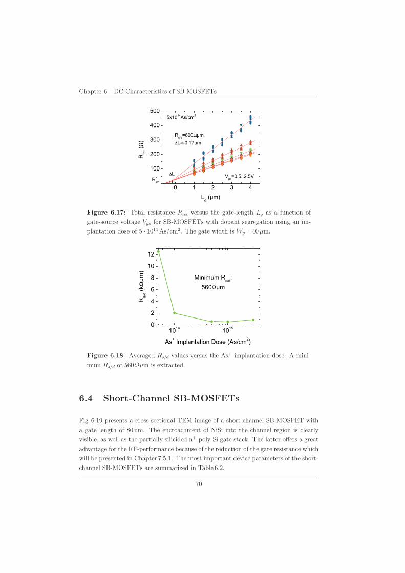
Chapter 6. DC-Characteristics of SB-MOSFETs
0 1 2 3 4
100
200
300
400
500
'
#$�"%&��Ω��Δ'%(�)*+��
Rto
t (Ω)
', ����
Δ'#$�"
-�*�*.�$����
/,$%�)-))�)-/
Figure 6.17: Total resistance Rtot versus the gate-length Lg as a function of
gate-source voltage Vgs for SB-MOSFETs with dopant segregation using an im-
plantation dose of 5 · 1014 As/cm2. The gate width is Wg = 40μm.
1014 10150
2
4
6
8
10
12
� ����Ω
��
�� � ������������ ����� ������
������ ��������
Figure 6.18: Averaged Rs/d values versus the As+ implantation dose. A mini-
mum Rs/d of 560 Ωμm is extracted.
6.4 Short-Channel SB-MOSFETs
Fig. 6.19 presents a cross-sectional TEM image of a short-channel SB-MOSFET with
a gate length of 80 nm. The encroachment of NiSi into the channel region is clearly
visible, as well as the partially silicided n+-poly-Si gate stack. The latter offers a great
advantage for the RF-performance because of the reduction of the gate resistance which
will be presented in Chapter 7.5.1. The most important device parameters of the short-
channel SB-MOSFETs are summarized in Table 6.2.
70
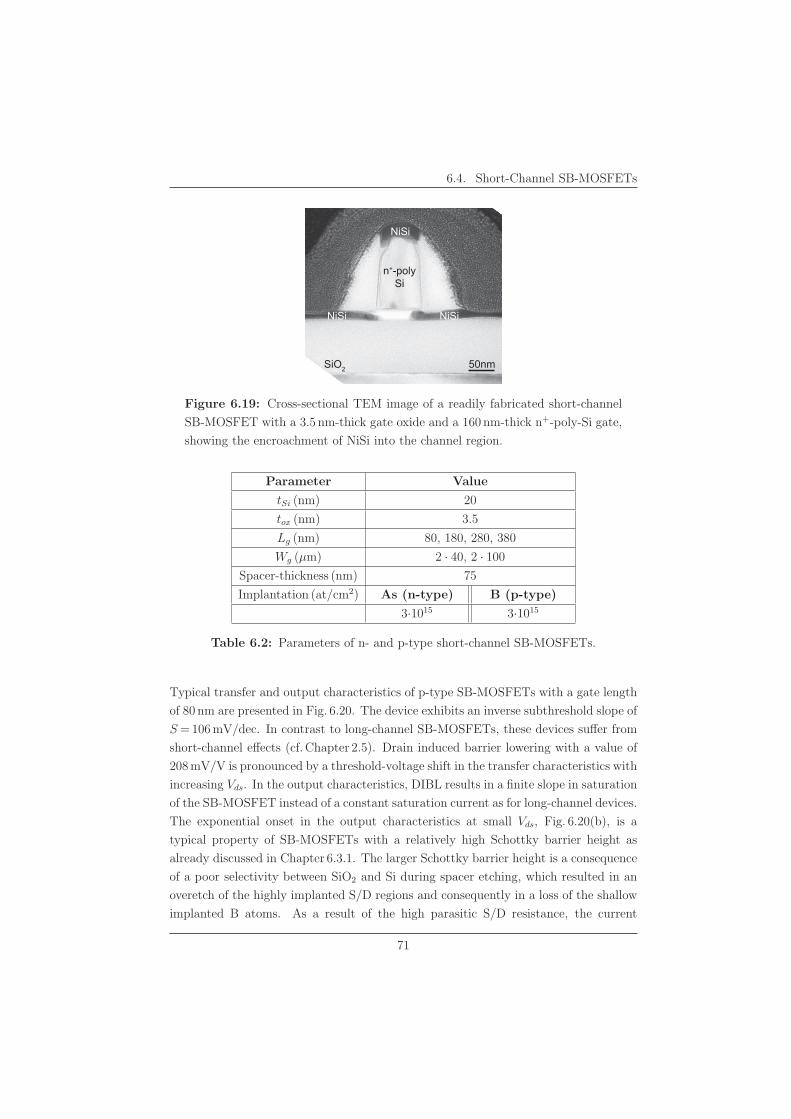
6.4. Short-Channel SB-MOSFETs
NiSi NiSi
NiSi
SiO2 50nm
n+-polySi
Figure 6.19: Cross-sectional TEM image of a readily fabricated short-channel
SB-MOSFET with a 3.5 nm-thick gate oxide and a 160 nm-thick n+-poly-Si gate,
showing the encroachment of NiSi into the channel region.
Parameter Value
tSi (nm) 20
tox (nm) 3.5
Lg (nm) 80, 180, 280, 380
Wg (μm) 2 · 40, 2 · 100
Spacer-thickness (nm) 75
Implantation (at/cm2) As (n-type) B (p-type)
3·1015 3·1015
Table 6.2: Parameters of n- and p-type short-channel SB-MOSFETs.
Typical transfer and output characteristics of p-type SB-MOSFETs with a gate length
of 80 nm are presented in Fig. 6.20. The device exhibits an inverse subthreshold slope of
S = 106 mV/dec. In contrast to long-channel SB-MOSFETs, these devices suffer from
short-channel effects (cf. Chapter 2.5). Drain induced barrier lowering with a value of
208 mV/V is pronounced by a threshold-voltage shift in the transfer characteristics with
increasing Vds. In the output characteristics, DIBL results in a finite slope in saturation
of the SB-MOSFET instead of a constant saturation current as for long-channel devices.
The exponential onset in the output characteristics at small Vds, Fig. 6.20(b), is a
typical property of SB-MOSFETs with a relatively high Schottky barrier height as
already discussed in Chapter 6.3.1. The larger Schottky barrier height is a consequence
of a poor selectivity between SiO2 and Si during spacer etching, which resulted in an
overetch of the highly implanted S/D regions and consequently in a loss of the shallow
implanted B atoms. As a result of the high parasitic S/D resistance, the current
71
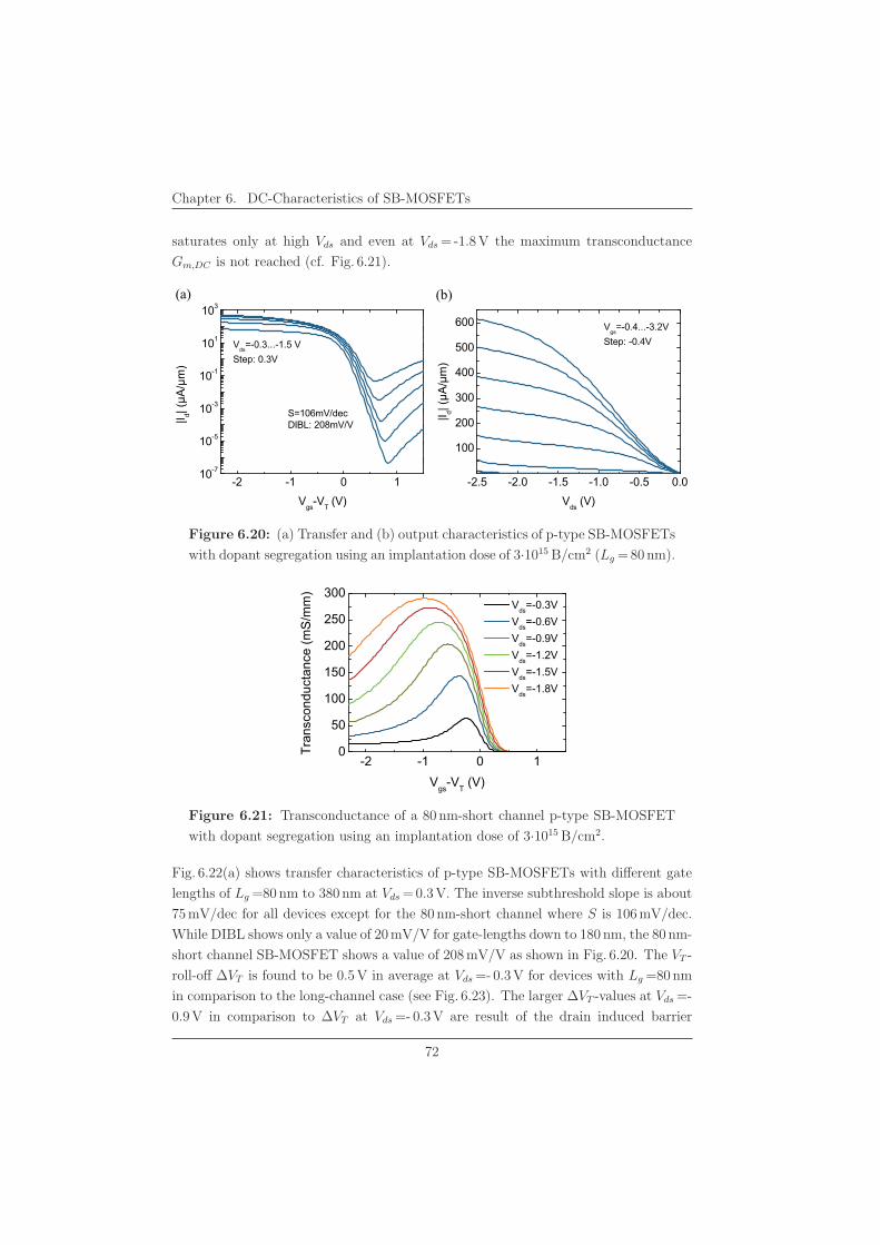
Chapter 6. DC-Characteristics of SB-MOSFETs
saturates only at high Vds and even at Vds = -1.8 V the maximum transconductance
Gm,DC is not reached (cf. Fig. 6.21).
-2.5 -2.0 -1.5 -1.0 -0.5 0.0
100
200
300
400
500
600
-2 -1 0 110-7
10-5
10-3
10-1
101
103(a)
Vgs
=-0.4...-3.2VStep: -0.4V
�� ������
��
Vds
(V)
(b)
�
�� ������
��
Vgs
-VT (V)
Vds
=-0.3...-1.5 VStep: 0.3V
S=106mV/decDIBL: 208mV/V
Figure 6.20: (a) Transfer and (b) output characteristics of p-type SB-MOSFETs
with dopant segregation using an implantation dose of 3·1015 B/cm2 (Lg = 80 nm).
-2 -1 0 10
50
100
150
200
250
300
Tran
scon
duct
ance
(mS
/mm
)
Vgs-VT (V)
Vds=-0.3V Vds=-0.6V Vds=-0.9V Vds=-1.2V Vds=-1.5V Vds=-1.8V
Figure 6.21: Transconductance of a 80 nm-short channel p-type SB-MOSFET
with dopant segregation using an implantation dose of 3·1015 B/cm2.
Fig. 6.22(a) shows transfer characteristics of p-type SB-MOSFETs with different gate
lengths of Lg =80 nm to 380 nm at Vds = 0.3 V. The inverse subthreshold slope is about
75 mV/dec for all devices except for the 80 nm-short channel where S is 106 mV/dec.
While DIBL shows only a value of 20 mV/V for gate-lengths down to 180 nm, the 80 nm-
short channel SB-MOSFET shows a value of 208 mV/V as shown in Fig. 6.20. The VT -
roll-off ΔVT is found to be 0.5 V in average at Vds =- 0.3 V for devices with Lg =80 nm
in comparison to the long-channel case (see Fig. 6.23). The larger ΔVT -values at Vds =-
0.9 V in comparison to ΔVT at Vds =- 0.3 V are result of the drain induced barrier
72
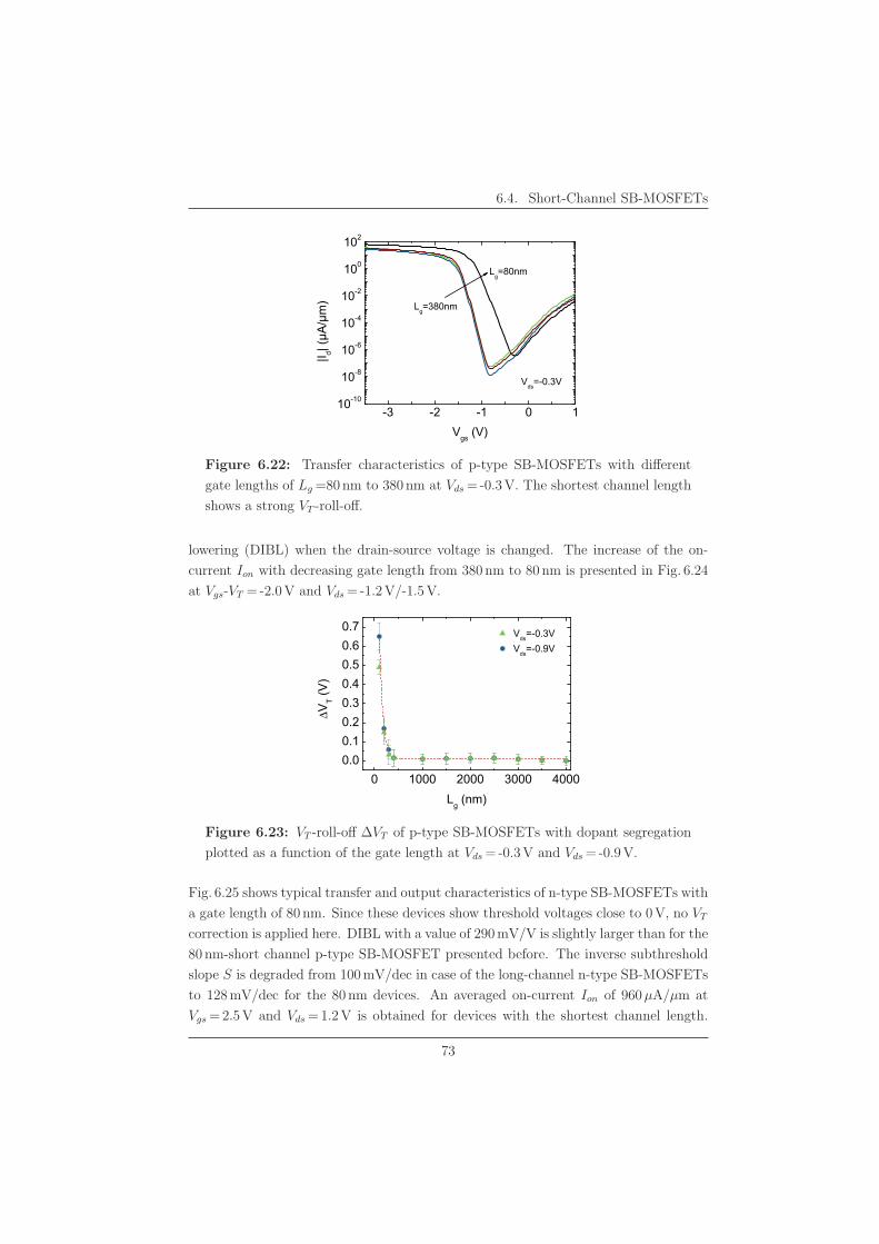
6.4. Short-Channel SB-MOSFETs
-3 -2 -1 0 110-10
10-8
10-6
10-4
10-2
100
102
�� ������
��
Vgs (V)
Lg=80nm
Lg=380nm
Vds=-0.3V
Figure 6.22: Transfer characteristics of p-type SB-MOSFETs with different
gate lengths of Lg =80 nm to 380 nm at Vds = -0.3 V. The shortest channel length
shows a strong VT -roll-off.
lowering (DIBL) when the drain-source voltage is changed. The increase of the on-
current Ion with decreasing gate length from 380 nm to 80 nm is presented in Fig. 6.24
at Vgs-VT = -2.0 V and Vds = -1.2 V/-1.5 V.
0 1000 2000 3000 40000.00.10.20.30.40.50.60.7 Vds=-0.3V
Vds=-0.9V
ΔVT (V
)
Lg (nm)
Figure 6.23: VT -roll-off ΔVT of p-type SB-MOSFETs with dopant segregation
plotted as a function of the gate length at Vds = -0.3 V and Vds = -0.9 V.
Fig. 6.25 shows typical transfer and output characteristics of n-type SB-MOSFETs with
a gate length of 80 nm. Since these devices show threshold voltages close to 0 V, no VT
correction is applied here. DIBL with a value of 290 mV/V is slightly larger than for the
80 nm-short channel p-type SB-MOSFET presented before. The inverse subthreshold
slope S is degraded from 100 mV/dec in case of the long-channel n-type SB-MOSFETs
to 128 mV/dec for the 80 nm devices. An averaged on-current Ion of 960μA/μm at
Vgs = 2.5 V and Vds = 1.2 V is obtained for devices with the shortest channel length.
73
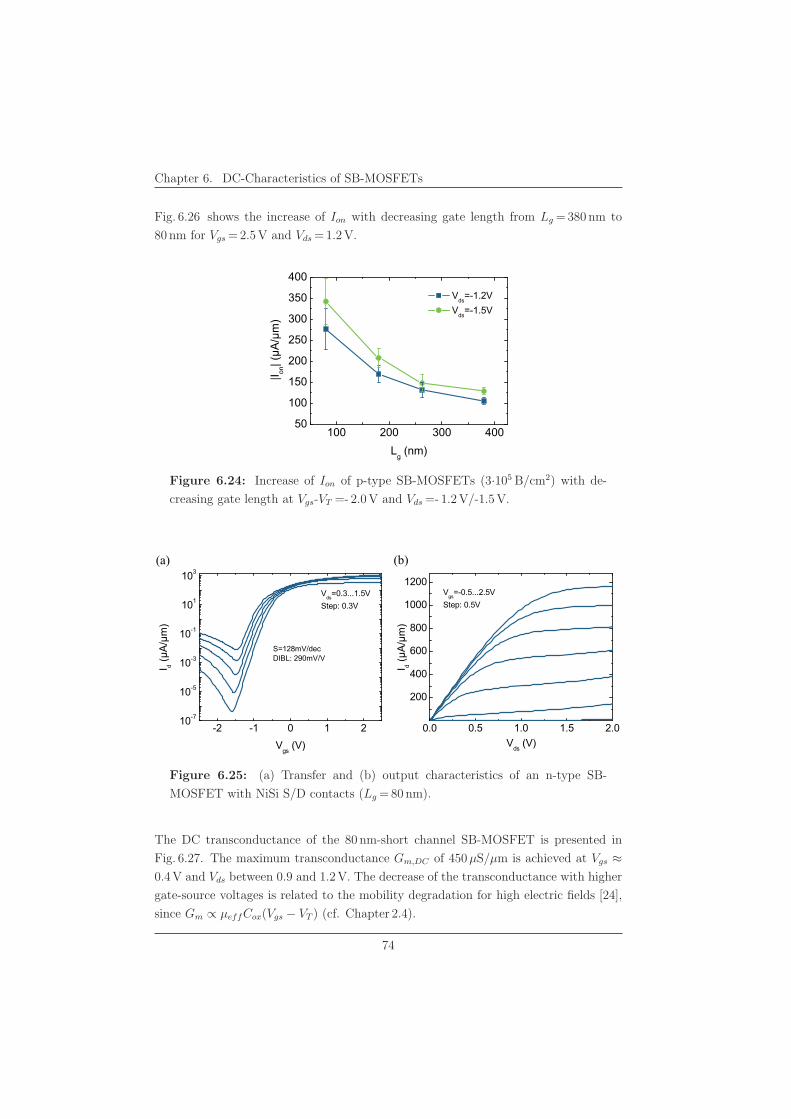
Chapter 6. DC-Characteristics of SB-MOSFETs
Fig. 6.26 shows the increase of Ion with decreasing gate length from Lg = 380 nm to
80 nm for Vgs = 2.5 V and Vds = 1.2 V.
100 200 300 40050
100
150
200
250
300
350
400 Vds=-1.2V Vds=-1.5V
�� ���������
Lg (nm)
Figure 6.24: Increase of Ion of p-type SB-MOSFETs (3·105 B/cm2) with de-
creasing gate length at Vgs-VT =- 2.0 V and Vds =- 1.2 V/-1.5 V.
0.0 0.5 1.0 1.5 2.0
200
400
600
800
1000
1200
-2 -1 0 1 210-7
10-5
10-3
10-1
101
103(a)
� ���������
Vds
(V)
Vgs=-0.5...2.5VStep: 0.5V
�
(b)
Vds=0.3...1.5VStep: 0.3V
� ���������
Vgs
(V)
S=128mV/decDIBL: 290mV/V
Figure 6.25: (a) Transfer and (b) output characteristics of an n-type SB-
MOSFET with NiSi S/D contacts (Lg = 80 nm).
The DC transconductance of the 80 nm-short channel SB-MOSFET is presented in
Fig. 6.27. The maximum transconductance Gm,DC of 450μS/μm is achieved at Vgs ≈0.4 V and Vds between 0.9 and 1.2 V. The decrease of the transconductance with higher
gate-source voltages is related to the mobility degradation for high electric fields [24],
since Gm ∝ μeffCox(Vgs − VT ) (cf. Chapter 2.4).
74
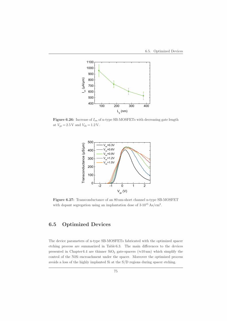
6.5. Optimized Devices
100 200 300 400400
500
600
700
800
900
1000
1100
� ���������
Lg (nm)
Figure 6.26: Increase of Ion of n-type SB-MOSFETs with decreasing gate length
at Vgs = 2.5 V and Vds = 1.2 V.
-2 -1 0 1 20
100
200
300
400
500
����
���
������
�����
���
Vgs (V)
Vds=0.3V Vds=0.6V Vds=0.9V Vds=1.2V Vds=1.5V
Figure 6.27: Transconductance of an 80 nm-short channel n-type SB-MOSFET
with dopant segregation using an implantation dose of 3·1015 As/cm2.
6.5 Optimized Devices
The device parameters of n-type SB-MOSFETs fabricated with the optimized spacer
etching process are summarized in Table 6.3. The main differences to the devices
presented in Chapter 6.4 are thinner SiO2 gate-spacers (≈10 nm) which simplify the
control of the NiSi encroachment under the spacer. Moreover the optimized process
avoids a loss of the highly implanted Si at the S/D regions during spacer etching.
75
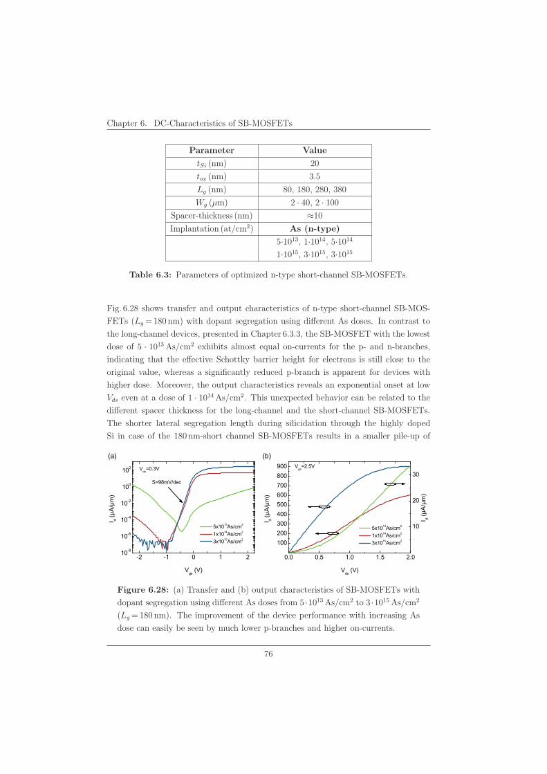
Chapter 6. DC-Characteristics of SB-MOSFETs
Parameter Value
tSi (nm) 20
tox (nm) 3.5
Lg (nm) 80, 180, 280, 380
Wg (μm) 2 · 40, 2 · 100
Spacer-thickness (nm) ≈10
Implantation (at/cm2) As (n-type)
5·1013, 1·1014, 5·1014
1·1015, 3·1015, 3·1015
Table 6.3: Parameters of optimized n-type short-channel SB-MOSFETs.
Fig. 6.28 shows transfer and output characteristics of n-type short-channel SB-MOS-
FETs (Lg = 180 nm) with dopant segregation using different As doses. In contrast to
the long-channel devices, presented in Chapter 6.3.3, the SB-MOSFET with the lowest
dose of 5 · 1013 As/cm2 exhibits almost equal on-currents for the p- and n-branches,
indicating that the effective Schottky barrier height for electrons is still close to the
original value, whereas a significantly reduced p-branch is apparent for devices with
higher dose. Moreover, the output characteristics reveals an exponential onset at low
Vds even at a dose of 1 · 1014 As/cm2. This unexpected behavior can be related to the
different spacer thickness for the long-channel and the short-channel SB-MOSFETs.
The shorter lateral segregation length during silicidation through the highly doped
Si in case of the 180 nm-short channel SB-MOSFETs results in a smaller pile-up of
-2 -1 0 1 210-8
10-6
10-4
10-2
100
102
0.0 0.5 1.0 1.5 2.0
100200300400500600700800900
Vgs
(V)
5x10¹³As/cm2
1x10¹⁴As/cm2
3x10¹⁵As/cm2
Vds
=0.3V
S=98mV/dec
(b)
Vds
(V)
5x10¹³As/cm2
1x10¹⁴As/cm2
3x10¹⁵As/cm2
Vgs
=2.5V
(a)
10
20
30
Figure 6.28: (a) Transfer and (b) output characteristics of SB-MOSFETs with
dopant segregation using different As doses from 5 ·1013 As/cm2 to 3 ·1015 As/cm2
(Lg = 180 nm). The improvement of the device performance with increasing As
dose can easily be seen by much lower p-branches and higher on-currents.
76
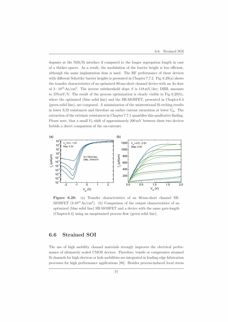
6.6. Strained SOI
dopants at the NiSi/Si interface if compared to the longer segregation length in case
of a thicker spacer. As a result, the modulation of the barrier height is less efficient,
although the same implantation dose is used. The RF performance of these devices
with different Schottky barrier heights is presented in Chapter 7.7.2. Fig. 6.29(a) shows
the transfer characteristics of an optimized 80 nm-short channel device with an As dose
of 3 · 1015 As/cm2. The inverse subthreshold slope S is 118 mV/dec; DIBL amounts
to 370 mV/V. The result of the process optimization is clearly visible in Fig. 6.29(b),
where the optimized (blue solid line) and the SB-MOSFET, presented in Chapter 6.4
(green solid line), are compared. A minimization of the unintentional Si-etching results
in lower S/D resistances and therefore an earlier current saturation at lower Vds. The
extraction of the extrinsic resistances in Chapter 7.7.1 quantifies this qualitative finding.
Please note, that a small VT -shift of approximately 200 mV between these two devices
forbids a direct comparison of the on-currents.
-2 -1 0 1 210-710-610-510-410-310-210-1100101102103
0.0 0.5 1.0 1.5 2.0
200
400
600
800
1000
1200
� �������
Vgs
(V)
Vds=0.3...1.2VStep: 0.3V
S=118mV/decDIBL: 370mV/V
(b)
� �������
Vds
(V)
Vgs
=-0.5...2.5VStep: 0.5V
(a)
Figure 6.29: (a) Transfer characteristics of an 80 nm-short channel SB-
MOSFET (3·1015 As/cm2). (b) Comparison of the output characteristics of an
optimized (blue solid line) SB-MOSFET and a device with the same gate-length
(Chapter 6.4) using an unoptimized process flow (green solid line).
6.6 Strained SOI
The use of high mobility channel materials strongly improves the electrical perfor-
mance of ultimately scaled CMOS devices. Therefore, tensile or compressive strained
Si channels for high electron or hole mobilities are integrated in leading edge fabrication
processes for high performance applications [88]. Besides process-induced local stress
77
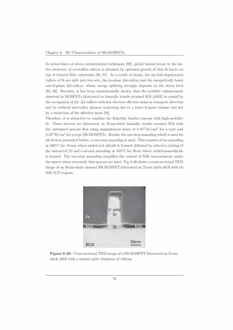
Chapter 6. DC-Characteristics of SB-MOSFETs
by stress liners or stress memorization techniques [89], global biaxial strain in the lat-
tice structure of crystalline silicon is obtained by epitaxial growth of thin Si layers on
top of relaxed SiGe substrates [90, 91]. As a result of strain, the six-fold degenerated
valleys of Si are split into two sets, the in-plane Δ4-valleys and the energetically lower
out-of-plane Δ2-valleys, whose energy splitting strongly depends on the stress level
[92, 93]. Recently, it has been experimentally shown, that the mobility enhancement
observed in MOSFETs fabricated on biaxially tensile strained SOI (sSOI) is caused by
the occupation of the Δ2-valleys with low electron effective mass in transport direction
and by reduced intervalley phonon scattering due to a lower k-space volume and not
by a reduction of the effective mass [94].
Therefore, it is attractive to combine the Schottky barrier concept with high-mobility
Si. These devices are fabricated on 25 nm-thick biaxially tensile strained SOI with
the optimized process flow using implantation doses of 3·1015As/cm2 for n-type and
3·1015B/cm2 for p-type SB-MOSFETs. Besides the one-step annealing which is used for
all devices presented before, a two-step annealing is used. This consists of an annealing
at 280◦C for 10 min where nickel-rich silicide is formed, followed by selective etching of
the unreacted Ni and a second annealing at 450◦C for 30 sec where nickel-monosilicide
is formed. The two-step annealing simplifies the control of NiSi encroachment under
the spacer when extremely thin spacers are used. Fig. 6.30 shows a cross-sectional TEM
image of an 80 nm-short channel SB-MOSFET fabricated on 25 nm thick sSOI with its
NiSi S/D regions.
Figure 6.30: Cross-sectional TEM image of a SB-MOSFET fabricated on 25 nm-
thick sSOI with a buried oxide thickness of 140 nm.
78
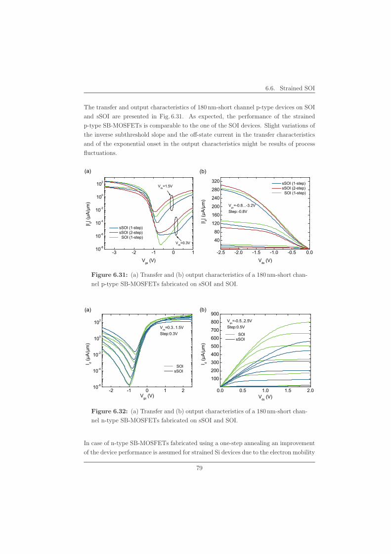
6.6. Strained SOI
The transfer and output characteristics of 180 nm-short channel p-type devices on SOI
and sSOI are presented in Fig. 6.31. As expected, the performance of the strained
p-type SB-MOSFETs is comparable to the one of the SOI devices. Slight variations of
the inverse subthreshold slope and the off-state current in the transfer characteristics
and of the exponential onset in the output characteristics might be results of process
fluctuations.
-3 -2 -1 0 110-8
10-6
10-4
10-2
100
102
-2.5 -2.0 -1.5 -1.0 -0.5 0.0
40
80
120
160
200
240
280
320
Vds=0.3V
!� "!���
����
Vgs
(V)
sSOI (1-step) sSOI (2-step) SOI (1-step)
Vds=1.5V sSOI (1-step) sSOI (2-step) SOI (1-step)
(b)
!� "!���
����
Vds
(V)
(a)
Vgs
=-0.8...-3.2VStep:-0.8V
Figure 6.31: (a) Transfer and (b) output characteristics of a 180 nm-short chan-
nel p-type SB-MOSFETs fabricated on sSOI and SOI.
-2 -1 0 1 210-6
10-4
10-2
100
102
0.0 0.5 1.0 1.5 2.0
100
200300400
500600700
800900
SOI sSOI
Vds
=0.3..1.5VStep:0.3V
� "�������
Vgs
(V)
SOI sSOI
(b)
� "�������
Vds
(V)
Vgs
=-0.5..2.5VStep:0.5V
(a)
Figure 6.32: (a) Transfer and (b) output characteristics of a 180 nm-short chan-
nel n-type SB-MOSFETs fabricated on sSOI and SOI.
In case of n-type SB-MOSFETs fabricated using a one-step annealing an improvement
of the device performance is assumed for strained Si devices due to the electron mobility
79
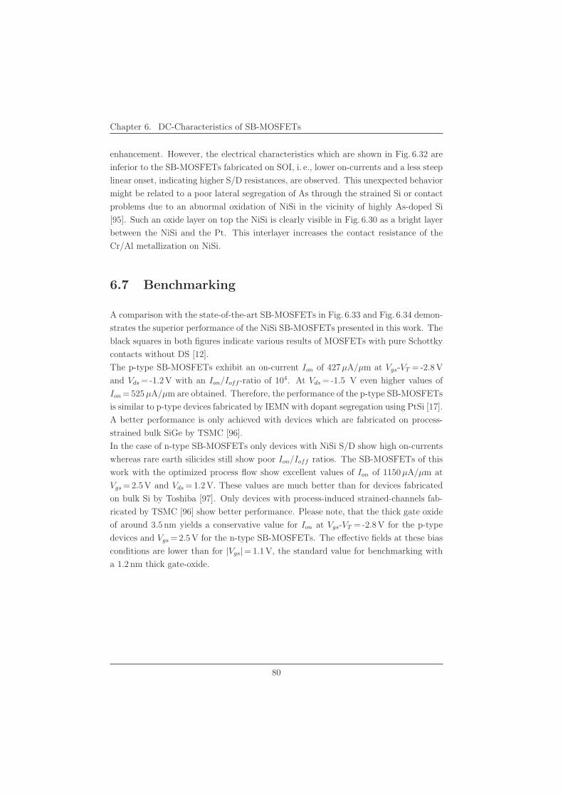
Chapter 6. DC-Characteristics of SB-MOSFETs
enhancement. However, the electrical characteristics which are shown in Fig. 6.32 are
inferior to the SB-MOSFETs fabricated on SOI, i. e., lower on-currents and a less steep
linear onset, indicating higher S/D resistances, are observed. This unexpected behavior
might be related to a poor lateral segregation of As through the strained Si or contact
problems due to an abnormal oxidation of NiSi in the vicinity of highly As-doped Si
[95]. Such an oxide layer on top the NiSi is clearly visible in Fig. 6.30 as a bright layer
between the NiSi and the Pt. This interlayer increases the contact resistance of the
Cr/Al metallization on NiSi.
6.7 Benchmarking
A comparison with the state-of-the-art SB-MOSFETs in Fig. 6.33 and Fig. 6.34 demon-
strates the superior performance of the NiSi SB-MOSFETs presented in this work. The
black squares in both figures indicate various results of MOSFETs with pure Schottky
contacts without DS [12].
The p-type SB-MOSFETs exhibit an on-current Ion of 427μA/μm at Vgs-VT = -2.8 V
and Vds = -1.2 V with an Ion/Ioff -ratio of 104. At Vds = -1.5 V even higher values of
Ion = 525μA/μm are obtained. Therefore, the performance of the p-type SB-MOSFETs
is similar to p-type devices fabricated by IEMN with dopant segregation using PtSi [17].
A better performance is only achieved with devices which are fabricated on process-
strained bulk SiGe by TSMC [96].
In the case of n-type SB-MOSFETs only devices with NiSi S/D show high on-currents
whereas rare earth silicides still show poor Ion/Ioff ratios. The SB-MOSFETs of this
work with the optimized process flow show excellent values of Ion of 1150μA/μm at
Vgs = 2.5 V and Vds = 1.2 V. These values are much better than for devices fabricated
on bulk Si by Toshiba [97]. Only devices with process-induced strained-channels fab-
ricated by TSMC [96] show better performance. Please note, that the thick gate oxide
of around 3.5 nm yields a conservative value for Ion at Vgs-VT = -2.8 V for the p-type
devices and Vgs = 2.5 V for the n-type SB-MOSFETs. The effective fields at these bias
conditions are lower than for |Vgs|= 1.1 V, the standard value for benchmarking with
a 1.2 nm thick gate-oxide.
80
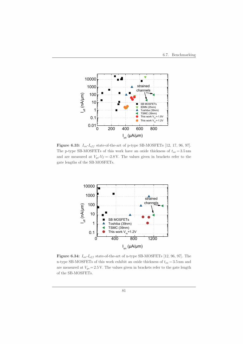
6.7. Benchmarking
0 200 400 600 8000.01
0.1
1
10
100
1000
10000
� �*� �+�, ��� $ ��� �-.���� �#�/���� ��0���� ����� ��0���� �/��� 1#2� 3
%��4��.3
� �/��� 1#2� 3%��4��-3
� � ����
��
$#�� �()�(��
������%�/����"�
Figure 6.33: Ion-Ioff state-of-the-art of p-type SB-MOSFETs [12, 17, 96, 97].
The p-type SB-MOSFETs of this work have an oxide thickness of tox = 3.5 nm
and are measured at Vgs-VT = -2.8 V. The values given in brackets refer to the
gate lengths of the SB-MOSFETs.
0 400 800 12000.1
1
10
100
1000
10000�
� ��� ������ �� ��� ������� ���� ������� � � ����� �������
� � ����
��
��� �!"#!��
$�� �%�&����%'
Figure 6.34: Ion-Ioff state-of-the-art of n-type SB-MOSFETs [12, 96, 97]. The
n-type SB-MOSFETs of this work exhibit an oxide thickness of tox = 3.5 nm and
are measured at Vgs = 2.5 V. The values given in brackets refer to the gate length
of the SB-MOSFETs.
81
Chapter 6. DC-Characteristics of SB-MOSFETs
6.8 Summary
A detailed study of long-channel as well as short-channel p- and n-type SB-MOSFETs
is presented. Devices with silicidation induced dopant segregation show drastically
improved DC performance when compared to SB-MOSFETs without ion implantation.
Thus, SB-MOSFETs with B segregation show an improved on-current by one order
of magnitude if compared to devices with pure NiSi S/D contacts. Studies of the
dopant dependence on the device performance show that the correct choice of the
implantation dose in combination with the spacer thickness, i. e., the segregation length,
is mandatory to achieve superior electrical characteristics. Generally, the analysis of the
devices shows that increasing the implantation dose results in a better performance of
the SB-MOSFETs with higher on-currents and a distinct suppression of the ambipolar
behavior. An extraction of the S/D resistances of long-channel n-type SB-MOSFETs
reveals a strong reduction for devices with high As dose. A minimum value of Rs/d of
560 Ωμm is extracted for SB-MOSFETs on 30 nm thick SOI.
The short-channel SB-MOSFETs with Lg = 80 nm show high performance comparable
to state-of-the-art devices. The on-currents are as high as 427μA/μm at Vgs-VT = -
2.8 V and Vds = -1.2 V for p-type SB-MOSFETs and 1150μA/μm at Vgs = 2.5 V and
Vds = 1.2 V for the n-type devices. Even higher values are expected by combination
of dopant segregation with elevated source and drain. Moreover, a reduction of the
natural length λ would result in a reduction of SCE, i. e., DIBL and VT -roll-off [98]. This
could be achieved by using thinner SOI, high-k gate-dielectrics or even different device
architectures like double gate or nanowire SB-MOSFETs, for instance. SB-MOSFETs
fabricated on biaxially strained SOI show similar DC performance for p-type devices
when compared with SOI devices. However, in case of n-type SB-MOSFETs, where a
performance increase is expected due to a higher effective electron mobility, degraded
performance is observed which could be a result of a worse segregation of As dopants
or a contact problem due to abnormal oxidation of NiSi in the presence of strained
silicon.
82
Chapter 7
RF-Characterization
This chapter provides a detailed radio-frequency (RF) analysis of dopant-segregated n-
and p-type SB-MOSFETs. The fundamentals of scattering S parameters and the small-
signal equivalent circuit of a MOSFET are introduced, followed by a brief description
of the characterization method and the measurement procedure. The extrinsic and
intrinsic device parameters are extracted as a function of the device dimensions, i. e.,
the gate length Lg and the gate width Wg. Finally, for the first time RF performance
of n-type SB-MOSFETs with dopant segregation using different implantation doses is
investigated. This provides an in-depth understanding of the frequency dependence
of SB-MOSFETs having different Schottky barrier heights. A comparison with state-
of-the art devices demonstrates the superior performance of the 80 nm-short channel
devices.
7.1 Scattering-Parameters
Scattering or S-parameters are used for the characterization of n-port networks and
allow an extraction of important figures of merit such as the cut-off frequency fT and
the maximum oscillation frequency fmax. Although, various other network analysis
methods exist [99, 100], S-parameters hold the advantage that no open and short
circuits are required for measurements whereas H-, Y - and Z-parameter sets which
relate total voltages and total currents at each of the two ports rely on short and
open measurements. This is a crucial point for the RF characterization because of the
difficulty to achieve short and open over a broad band of frequencies.
For the characterization of a two-port network the scattering matrix (S) relates the
power levels of the incident (a1, a2) and reflected waves (b1, b2) at the input (1) and
83
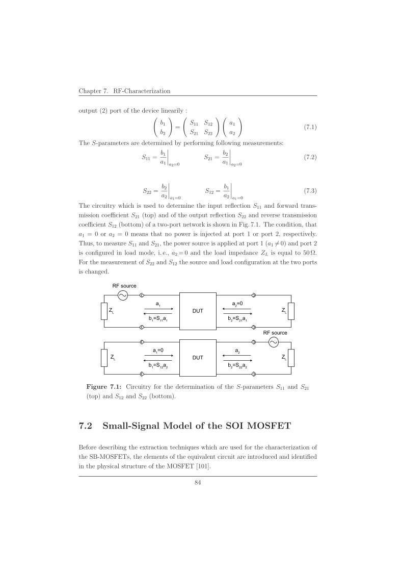
Chapter 7. RF-Characterization
output (2) port of the device linearily :(b1
b2
)=
(S11 S12
S21 S22
) (a1
a2
)(7.1)
The S-parameters are determined by performing following measurements:
S11 =b1
a1
∣∣∣∣a2=0
S21 =b2
a1
∣∣∣∣a2=0
(7.2)
S22 =b2
a2
∣∣∣∣a1=0
S12 =b1
a2
∣∣∣∣a1=0
(7.3)
The circuitry which is used to determine the input reflection S11 and forward trans-
mission coefficient S21 (top) and of the output reflection S22 and reverse transmission
coefficient S12 (bottom) of a two-port network is shown in Fig. 7.1. The condition, that
a1 = 0 or a2 = 0 means that no power is injected at port 1 or port 2, respectively.
Thus, to measure S11 and S21, the power source is applied at port 1 (a1 �= 0) and port 2
is configured in load mode, i. e., a2 = 0 and the load impedance ZL is equal to 50 Ω.
For the measurement of S22 and S12 the source and load configuration at the two ports
is changed.
DUTa1
b1=S11a1
a2=0
b2=S21a1
ZL
ZL
ZL
DUTa1=0
b1=S12a2
a2
b2=S22a2
ZL
RF source
RF source
Figure 7.1: Circuitry for the determination of the S-parameters S11 and S21
(top) and S12 and S22 (bottom).
7.2 Small-Signal Model of the SOI MOSFET
Before describing the extraction techniques which are used for the characterization of
the SB-MOSFETs, the elements of the equivalent circuit are introduced and identified
in the physical structure of the MOSFET [101].
84
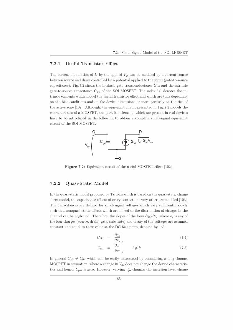
7.2. Small-Signal Model of the SOI MOSFET
7.2.1 Useful Transistor Effect
The current modulation of Id by the applied Vgs can be modeled by a current source
between source and drain controlled by a potential applied to the input (gate-to-source
capacitance). Fig. 7.2 shows the intrinsic gate transconductance Gmi and the intrinsic
gate-to-source capacitance Cgsi of the SOI MOSFET. The index ”i” denotes the in-
trinsic elements which model the useful transistor effect and which are thus dependent
on the bias conditions and on the device dimensions or more precisely on the size of
the active zone [102]. Although, the equivalent circuit presented in Fig. 7.2 models the
characteristics of a MOSFET, the parasitic elements which are present in real devices
have to be introduced in the following to obtain a complete small-signal equivalent
circuit of the SOI MOSFET.
G
CgsiVgs
Gmi
D
S
Id=GmiVgs
Figure 7.2: Equivalent circuit of the useful MOSFET effect [102].
7.2.2 Quasi-Static Model
In the quasi-static model proposed by Tsividis which is based on the quasi-static charge
sheet model, the capacitance effects of every contact on every other are modeled [103].
The capacitances are defined for small-signal voltages which vary sufficiently slowly
such that nonquasi-static effects which are linked to the distribution of charges in the
channel can be neglected. Therefore, the slopes of the form ∂qk/∂vl, where qk is any of
the four charges (source, drain, gate, substrate) and vl any of the voltages are assumed
constant and equal to their value at the DC bias point, denoted by ”o”:
Ckki =∂qk
∂vk
∣∣∣∣o
(7.4)
Ckli =∂qk
∂vl
∣∣∣∣o
l �= k (7.5)
In general Ckli �= Clki which can be easily unterstood by considering a long-channel
MOSFET in saturation, where a change in Vds does not change the device characteris-
tics and hence, Cgdi is zero. However, varying Vgs changes the inversion layer charge
85
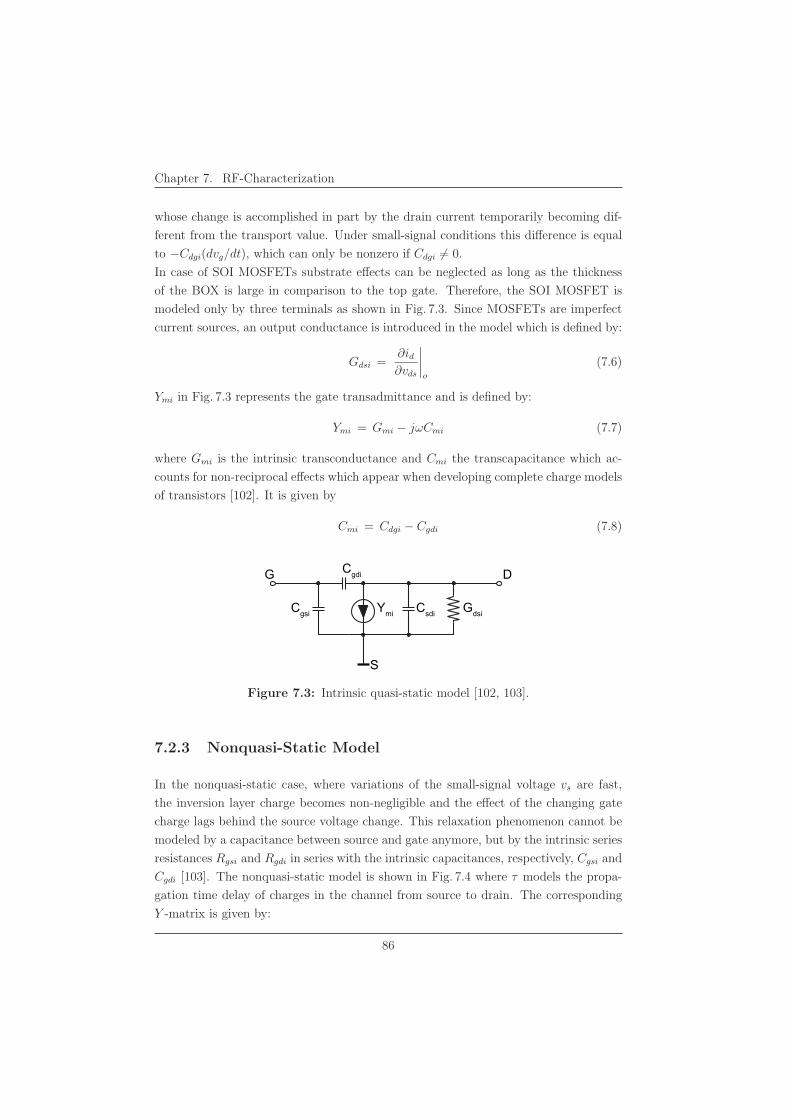
Chapter 7. RF-Characterization
whose change is accomplished in part by the drain current temporarily becoming dif-
ferent from the transport value. Under small-signal conditions this difference is equal
to −Cdgi(dvg/dt), which can only be nonzero if Cdgi �= 0.
In case of SOI MOSFETs substrate effects can be neglected as long as the thickness
of the BOX is large in comparison to the top gate. Therefore, the SOI MOSFET is
modeled only by three terminals as shown in Fig. 7.3. Since MOSFETs are imperfect
current sources, an output conductance is introduced in the model which is defined by:
Gdsi =∂id∂vds
∣∣∣∣o
(7.6)
Ymi in Fig. 7.3 represents the gate transadmittance and is defined by:
Ymi = Gmi − jωCmi (7.7)
where Gmi is the intrinsic transconductance and Cmi the transcapacitance which ac-
counts for non-reciprocal effects which appear when developing complete charge models
of transistors [102]. It is given by
Cmi = Cdgi − Cgdi (7.8)
G
Cgsi Csdi
Cgdi
Gdsi
D
S
Ymi
Figure 7.3: Intrinsic quasi-static model [102, 103].
7.2.3 Nonquasi-Static Model
In the nonquasi-static case, where variations of the small-signal voltage vs are fast,
the inversion layer charge becomes non-negligible and the effect of the changing gate
charge lags behind the source voltage change. This relaxation phenomenon cannot be
modeled by a capacitance between source and gate anymore, but by the intrinsic series
resistances Rgsi and Rgdi in series with the intrinsic capacitances, respectively, Cgsi and
Cgdi [103]. The nonquasi-static model is shown in Fig. 7.4 where τ models the propa-
gation time delay of charges in the channel from source to drain. The corresponding
Y -matrix is given by:
86
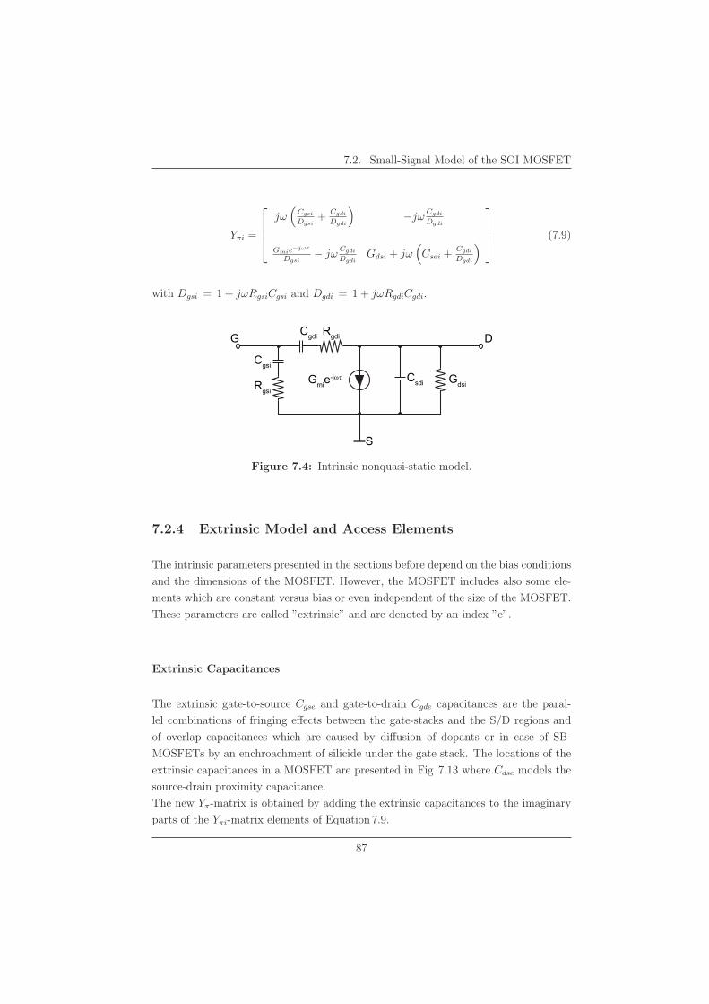
7.2. Small-Signal Model of the SOI MOSFET
Yπi =
⎡⎢⎢⎣
jω(
Cgsi
Dgsi+
Cgdi
Dgdi
)−jω
Cgdi
Dgdi
Gmie−jωτ
Dgsi− jω
Cgdi
DgdiGdsi + jω
(Csdi +
Cgdi
Dgdi
)⎤⎥⎥⎦ (7.9)
with Dgsi = 1 + jωRgsiCgsi and Dgdi = 1 + jωRgdiCgdi.
G
Cgsi
Rgsi
Csdi
Cgdi Rgdi
Gdsi
D
S
Gmie-jωτ
Figure 7.4: Intrinsic nonquasi-static model.
7.2.4 Extrinsic Model and Access Elements
The intrinsic parameters presented in the sections before depend on the bias conditions
and the dimensions of the MOSFET. However, the MOSFET includes also some ele-
ments which are constant versus bias or even independent of the size of the MOSFET.
These parameters are called ”extrinsic” and are denoted by an index ”e”.
Extrinsic Capacitances
The extrinsic gate-to-source Cgse and gate-to-drain Cgde capacitances are the paral-
lel combinations of fringing effects between the gate-stacks and the S/D regions and
of overlap capacitances which are caused by diffusion of dopants or in case of SB-
MOSFETs by an enchroachment of silicide under the gate stack. The locations of the
extrinsic capacitances in a MOSFET are presented in Fig. 7.13 where Cdse models the
source-drain proximity capacitance.
The new Yπ-matrix is obtained by adding the extrinsic capacitances to the imaginary
parts of the Yπi-matrix elements of Equation 7.9.
87
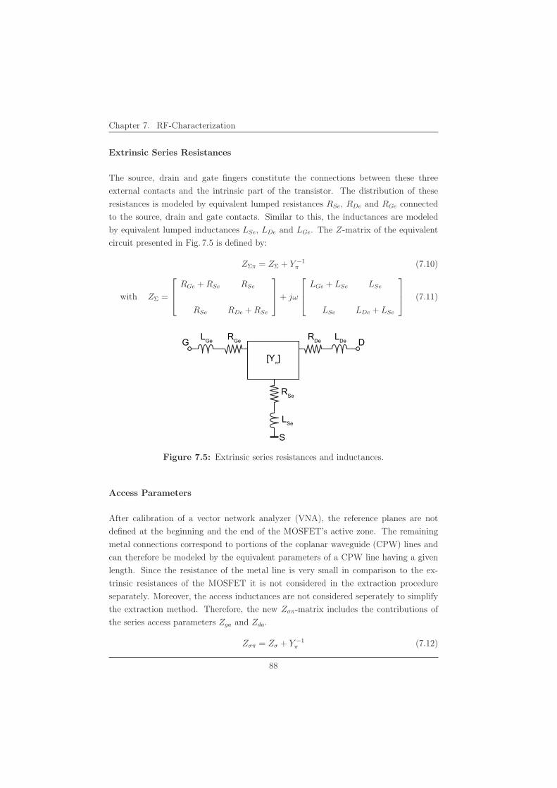
Chapter 7. RF-Characterization
Extrinsic Series Resistances
The source, drain and gate fingers constitute the connections between these three
external contacts and the intrinsic part of the transistor. The distribution of these
resistances is modeled by equivalent lumped resistances RSe, RDe and RGe connected
to the source, drain and gate contacts. Similar to this, the inductances are modeled
by equivalent lumped inductances LSe, LDe and LGe. The Z-matrix of the equivalent
circuit presented in Fig. 7.5 is defined by:
ZΣπ = ZΣ + Y −1π (7.10)
with ZΣ =
⎡⎢⎣
RGe + RSe RSe
RSe RDe + RSe
⎤⎥⎦ + jω
⎡⎢⎣
LGe + LSe LSe
LSe LDe + LSe
⎤⎥⎦ (7.11)
G LGe RGe RDe LDe
RSe
LSe
D
S
[Yπ]
Figure 7.5: Extrinsic series resistances and inductances.
Access Parameters
After calibration of a vector network analyzer (VNA), the reference planes are not
defined at the beginning and the end of the MOSFET’s active zone. The remaining
metal connections correspond to portions of the coplanar waveguide (CPW) lines and
can therefore be modeled by the equivalent parameters of a CPW line having a given
length. Since the resistance of the metal line is very small in comparison to the ex-
trinsic resistances of the MOSFET it is not considered in the extraction procedure
separately. Moreover, the access inductances are not considered seperately to simplify
the extraction method. Therefore, the new Zσπ-matrix includes the contributions of
the series access parameters Zga and Zda.
Zσπ = Zσ + Y −1π (7.12)
88
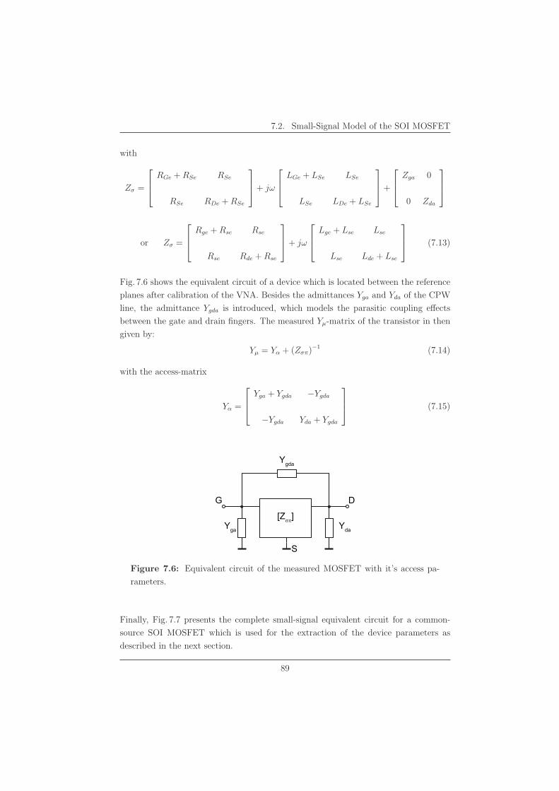
7.2. Small-Signal Model of the SOI MOSFET
with
Zσ =
⎡⎢⎣
RGe + RSe RSe
RSe RDe + RSe
⎤⎥⎦ + jω
⎡⎢⎣
LGe + LSe LSe
LSe LDe + LSe
⎤⎥⎦ +
⎡⎢⎣
Zga 0
0 Zda
⎤⎥⎦
or Zσ =
⎡⎢⎣
Rge + Rse Rse
Rse Rde + Rse
⎤⎥⎦ + jω
⎡⎢⎣
Lge + Lse Lse
Lse Lde + Lse
⎤⎥⎦ (7.13)
Fig. 7.6 shows the equivalent circuit of a device which is located between the reference
planes after calibration of the VNA. Besides the admittances Yga and Yda of the CPW
line, the admittance Ygda is introduced, which models the parasitic coupling effects
between the gate and drain fingers. The measured Yμ-matrix of the transistor in then
given by:
Yμ = Yα + (Zσπ)−1 (7.14)
with the access-matrix
Yα =
⎡⎢⎣
Yga + Ygda −Ygda
−Ygda Yda + Ygda
⎤⎥⎦ (7.15)
G D
S
[Zσπ]
Ygda
YdaYga
Figure 7.6: Equivalent circuit of the measured MOSFET with it’s access pa-
rameters.
Finally, Fig. 7.7 presents the complete small-signal equivalent circuit for a common-
source SOI MOSFET which is used for the extraction of the device parameters as
described in the next section.
89
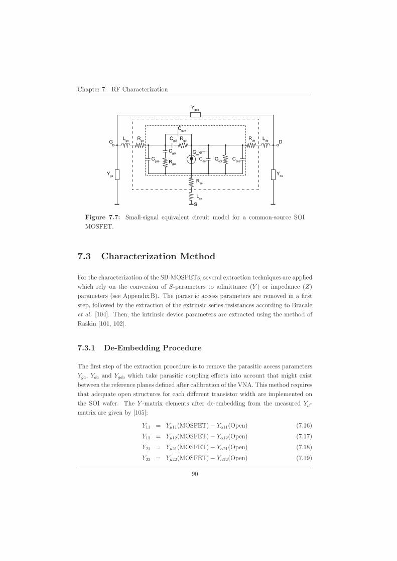
Chapter 7. RF-Characterization
Cgse
Yga
Rge Rde
Rse
Cdsi Cdse
Cgdi Rgdi
Cgde
Gsdi
D
S
Gmie-jωτ
Yda
Cgsi
Rgsi
GLge Lde
Lse
Ygda
Figure 7.7: Small-signal equivalent circuit model for a common-source SOI
MOSFET.
7.3 Characterization Method
For the characterization of the SB-MOSFETs, several extraction techniques are applied
which rely on the conversion of S-parameters to admittance (Y ) or impedance (Z)
parameters (see Appendix B). The parasitic access parameters are removed in a first
step, followed by the extraction of the extrinsic series resistances according to Bracale
et al. [104]. Then, the intrinsic device parameters are extracted using the method of
Raskin [101, 102].
7.3.1 De-Embedding Procedure
The first step of the extraction procedure is to remove the parasitic access parameters
Yga, Yda and Ygda which take parasitic coupling effects into account that might exist
between the reference planes defined after calibration of the VNA. This method requires
that adequate open structures for each different transistor width are implemented on
the SOI wafer. The Y -matrix elements after de-embedding from the measured Yμ-
matrix are given by [105]:
Y11 = Yμ11(MOSFET) − Yα11(Open) (7.16)
Y12 = Yμ12(MOSFET) − Yα12(Open) (7.17)
Y21 = Yμ21(MOSFET) − Yα21(Open) (7.18)
Y22 = Yμ22(MOSFET) − Yα22(Open) (7.19)
90
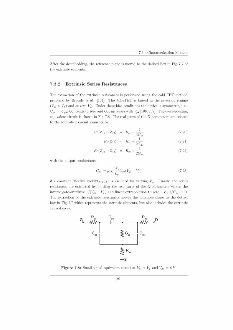
7.3. Characterization Method
After the deembedding, the reference plane is moved to the dashed box in Fig. 7.7 of
the extrinsic elements.
7.3.2 Extrinsic Series Resistances
The extraction of the extrinsic resistances is performed using the cold FET method
proposed by Bracale et al. [104]. The MOSFET is biased in the inversion regime
(Vgs > VT ) and at zero Vds. Under these bias conditions the device is symmetric, i. e.,
Cgs = Cgd, Gm tends to zero and Gds increases with Vgs [106, 107]. The corresponding
equivalent circuit is shown in Fig. 7.8. The real parts of the Z-parameters are related
to the equivalent circuit elements by:
Re(Z11 − Z12) = Rge − 1
4Gds
(7.20)
Re(Z12) = Rse +1
2Gds
(7.21)
Re(Z22 − Z12) = Rde +1
2Gds
(7.22)
with the output conductance
Gds = μeffWg
Lg
Cox(Vgs − VT ) (7.23)
if a constant effective mobility μeff is assumed for varying Vgs. Finally, the series
resistances are extracted by plotting the real parts of the Z-parameters versus the
inverse gate-overdrive 1/(Vgs − VT ) and linear extrapolation to zero, i. e., 1/Gds → 0.
The extraction of the extrinsic resistances moves the reference plane to the dotted
box in Fig. 7.7 which represents the intrinsic elements, but also includes the extrinsic
capacitances.
Cgs
Rge Rde
Rse
Cds
Cgd
Gds
D
S
G
Figure 7.8: Small-signal equivalent circuit at Vgs > VT and Vds = 0 V.
91
Chapter 7. RF-Characterization
7.3.3 Extraction of the Capacitances and Conductances
The capacitances and conductances of the devices are then obtained using the direct
extraction technique proposed by Raskin et al. [101, 102]. The extracted extrinsic
values are used to reconstruct the matrix Zσ which is substracted from Zσπ to de-
embed Yπ. The following analytical expressions result in the gate-to-source Cgs and
gate-to drain Cgd capacitance as well as in the intrinsic tranconductance Gmi and
output conductance Gdsi:
Gate-to-Source Capacitance Cgs
Cgs is composed of an extrinsic capacitance Cgse and an intrinsic capacitance Cgsi in
parallel. Cgse represents the overlap and fringing capacitances within the active zone.
Cgs = Cgsi + Cgse (7.24)
with
Cgse =1
ω[Im (Yπ11) + Im (Yπ12)] (7.25)
extracted at Vgs � VT and Vds = 0 V and
Cgsi =1
ω[Im (Yπ11) + Im (Yπ12) − ωCgse]
[1 +
(Re (Yπ11) + Re (Yπ12)
Im (Yπ11) + Im (Yπ12) − ωCgse
)2]
(7.26)
extracted from the Yπ-matrix measured at any arbitrarily chosen bias point.
Gate-to-Drain Capacitance Cgd
Cgd is composed of an extrinsic Cgde and an intrinsic Cgdi part in parallel. Cgde repre-
sents the overlap and fringing capacitances within the active zone.
Cgd = Cgdi + Cgde (7.27)
with
Cgde = − 1
ωIm (Yπ12) (7.28)
extracted at Vgs � VT and Vds = 0 V and
Cgdi = − 1
ω[Im (Yπ12) + ωCgde]
[1 +
(Re (Yπ12)
Im (Yπ12) + ωCgde
)2]
(7.29)
extracted from the Yπ-matrix measured at any arbitrarily chosen bias point.
92
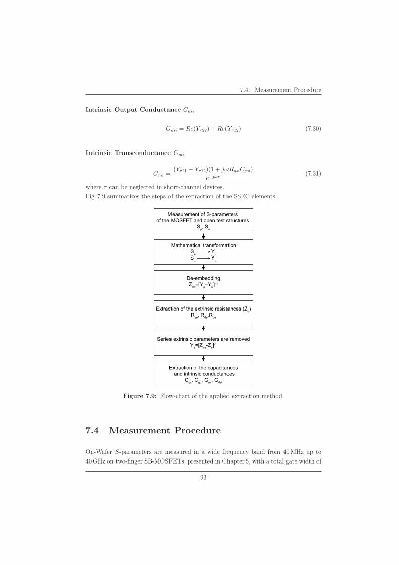
7.4. Measurement Procedure
Intrinsic Output Conductance Gdsi
Gdsi = Re(Yπ22) + Re(Yπ12) (7.30)
Intrinsic Transconductance Gmi
Gmi =(Yπ21 − Yπ12)(1 + jωRgsiCgsi)
e−jωτ(7.31)
where τ can be neglected in short-channel devices.
Fig. 7.9 summarizes the steps of the extraction of the SSEC elements.
Measurement of S-parameters of the MOSFET and open test structures
Sμ, Sα
Mathematical transformationSμ YμSα Yα
De-embeddingZσπ=[Yμ−Yα]
−1
Extraction of the extrinsic resistances (Zσ)Rse, Rde,Rge
Series extrinsic parameters are removedYπ=[Zσπ-Zσ]
-1
Extraction of the capacitances and intrinsic conductances
Cgs, Cgd, Gmi, Gdsi
Figure 7.9: Flow-chart of the applied extraction method.
7.4 Measurement Procedure
On-Wafer S-parameters are measured in a wide frequency band from 40 MHz up to
40 GHz on two-finger SB-MOSFETs, presented in Chapter 5, with a total gate width of
93
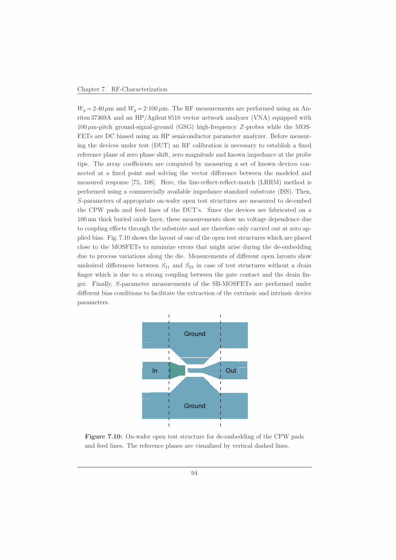
Chapter 7. RF-Characterization
Wg = 2·40μm and Wg = 2·100μm. The RF measurements are performed using an An-
ritsu 37369A and an HP/Agilent 8510 vector network analyzer (VNA) equipped with
100μm-pitch ground-signal-ground (GSG) high-frequency Z-probes while the MOS-
FETs are DC biased using an HP semiconductor parameter analyzer. Before measur-
ing the devices under test (DUT) an RF calibration is necessary to establish a fixed
reference plane of zero phase shift, zero magnitude and known impedance at the probe
tips. The array coefficients are computed by measuring a set of known devices con-
nected at a fixed point and solving the vector difference between the modeled and
measured response [75, 108]. Here, the line-reflect-reflect-match (LRRM) method is
performed using a commercially available impedance standard substrate (ISS). Then,
S-parameters of appropriate on-wafer open test structures are measured to de-embed
the CPW pads and feed lines of the DUT’s. Since the devices are fabricated on a
100 nm thick buried oxide layer, these measurements show no voltage dependence due
to coupling effects through the substrate and are therefore only carried out at zero ap-
plied bias. Fig. 7.10 shows the layout of one of the open test structures which are placed
close to the MOSFETs to minimize errors that might arise during the de-embedding
due to process variations along the die. Measurements of different open layouts show
undesired differences between S11 and S22 in case of test structures without a drain
finger which is due to a strong coupling between the gate contact and the drain fin-
ger. Finally, S-parameter measurements of the SB-MOSFETs are performed under
different bias conditions to facilitate the extraction of the extrinsic and intrinsic device
parameters.
Ground
OutIn
Ground
Figure 7.10: On-wafer open test structure for de-embedding of the CPW pads
and feed lines. The reference planes are visualized by vertical dashed lines.
94
7.5. Gate-Length Dependence
7.5 Gate-Length Dependence
7.5.1 Extrinsic Series Resistances
From the small-signal equivalent circuit, presented in Fig. 7.7, we extract the extrinsic
series resistances using the cold FET extraction procedure presented in Chapter 7.3.2.
Fig. 7.11 shows the source Rse, drain Rde and total S/D resistances Rse/de of p- and
n-type SB-MOSFETs with implantation doses of 3 · 1015B/cm2 and 3 · 1015As/cm2,
respectively. The difference in the values of Rse and Rde is due to an asymmetry be-
tween source and drain [109] which might be related to differences in the encroachment
of NiSi under the spacer. The decrease of Rse/de with the gate length is related to
Bracale’s extraction method and more precisely to the assumption made by Bracale
about the constant carrier mobility as a function of the applied gate-source voltage
[106, 110]. This assumption is not valid for thin gate dielectrics, like the used 3.5 nm
thick SiO2, where the carrier mobility decreases with increasing gate-source voltage.
The introduction of a mobility degradation factor results in an additional gate-length
dependent term in Equations 7.21-7.22 [106] which shows that Rse and Rde are over-
estimated if only one gate-length is considered. Therefore, the S/D resistances of the
SB-MOSFETs are obtained by extrapolation of the resistances to zero gate-length,
where the mobility degradation does not affect the extrapolation. The S/D resistance
of the n-type devices on the 20 nm-thick SOI substrate is Rse/de = 718 Ωμm, whereas a
value of Rse/de = 2.56 kΩμm is evident for the p-type devices. For n-type devices Rse/de
is comparable to the value of 600 Ωμm which is extracted from the DC characteristics
for SB-MOSFETs fabricated on 30 nm thick SOI in Chapter 6.3.4 if the thickness ratio
is taken into account. The higher Rse/de of the p-type SB-MOSFETs agrees well with
the DC characteristics shown in Fig. 6.20, where an exponential onset is still observed
in the output characteristics, indicating a high Schottky barrier height. These devices
suffered undesirably more during RIE-etching of the spacers. By optimizing the spacer
etching process, where the loss of highly doped Si at the S/D regions is minimized, a
similar Rse/de for p-type SB-MOSFETs as for n-type devices is expected since dopant
segregation results in Schottky barrier heights of around 0.1 eV for both, As and B
segregation (see Chapter 4.8).
Currently there is no known manufacturable solution for the requested 200 Ωμm on
fully depleted SOI (cf. ITRS Roadmap [2]). Therefore, the achieved Rse/de values seem
to be very promising, especially, when the fabrication process would be even more
optimized by combining dopant segregation with elevated S/D, for instance.
95
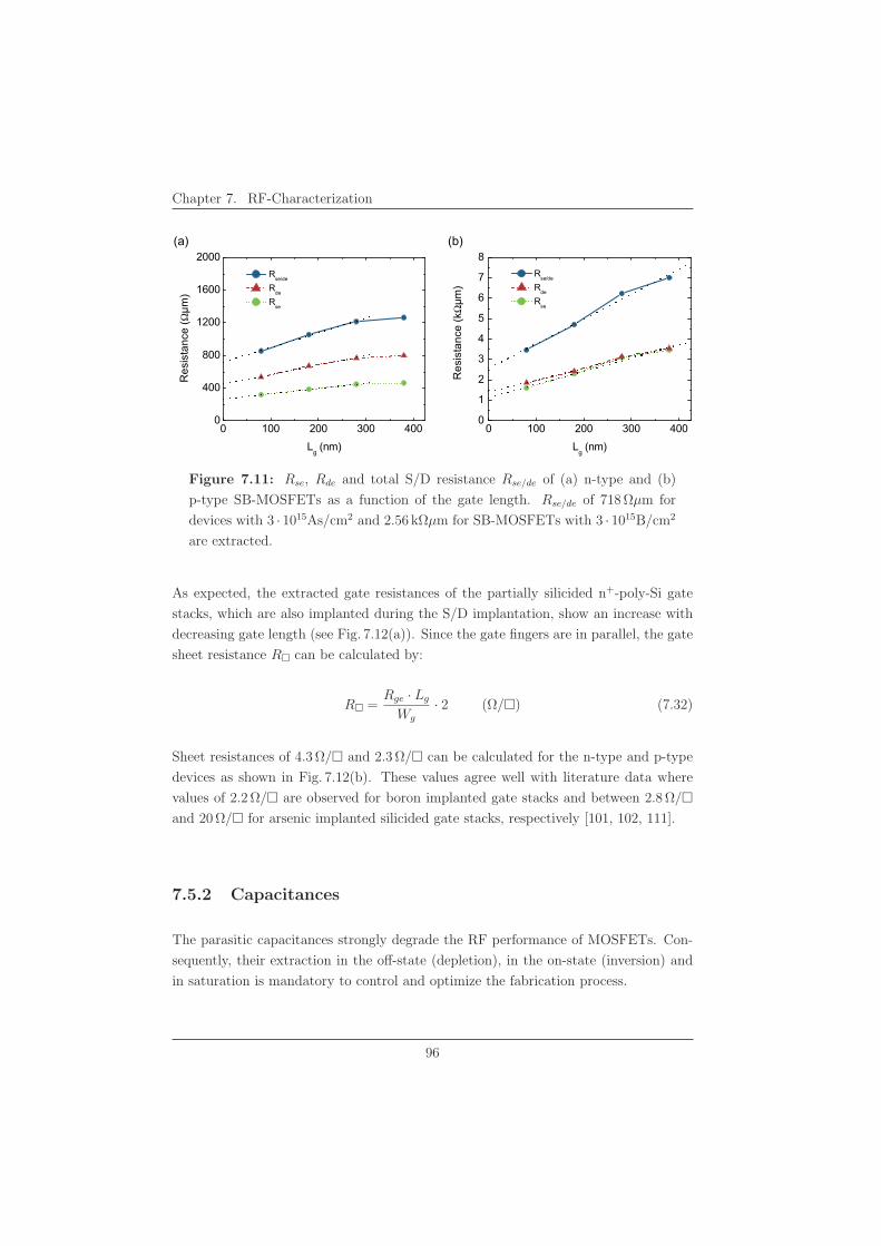
Chapter 7. RF-Characterization
0 100 200 300 4000
400
800
1200
1600
2000
0 100 200 300 4000
1
2
3
4
5
6
7
8
#�$�$��������
�
Lg (nm)
Rse/de
Rde
Rse
(b)
#�$�$�������
��
�L
g (nm)
Rse/de
Rde
Rse
(a)
Figure 7.11: Rse, Rde and total S/D resistance Rse/de of (a) n-type and (b)
p-type SB-MOSFETs as a function of the gate length. Rse/de of 718 Ωμm for
devices with 3 · 1015As/cm2 and 2.56 kΩμm for SB-MOSFETs with 3 · 1015B/cm2
are extracted.
As expected, the extracted gate resistances of the partially silicided n+-poly-Si gate
stacks, which are also implanted during the S/D implantation, show an increase with
decreasing gate length (see Fig. 7.12(a)). Since the gate fingers are in parallel, the gate
sheet resistance R� can be calculated by:
R� =Rge · Lg
Wg
· 2 (Ω/�) (7.32)
Sheet resistances of 4.3 Ω/� and 2.3 Ω/� can be calculated for the n-type and p-type
devices as shown in Fig. 7.12(b). These values agree well with literature data where
values of 2.2 Ω/� are observed for boron implanted gate stacks and between 2.8 Ω/�and 20 Ω/� for arsenic implanted silicided gate stacks, respectively [101, 102, 111].
7.5.2 Capacitances
The parasitic capacitances strongly degrade the RF performance of MOSFETs. Con-
sequently, their extraction in the off-state (depletion), in the on-state (inversion) and
in saturation is mandatory to control and optimize the fabrication process.
96
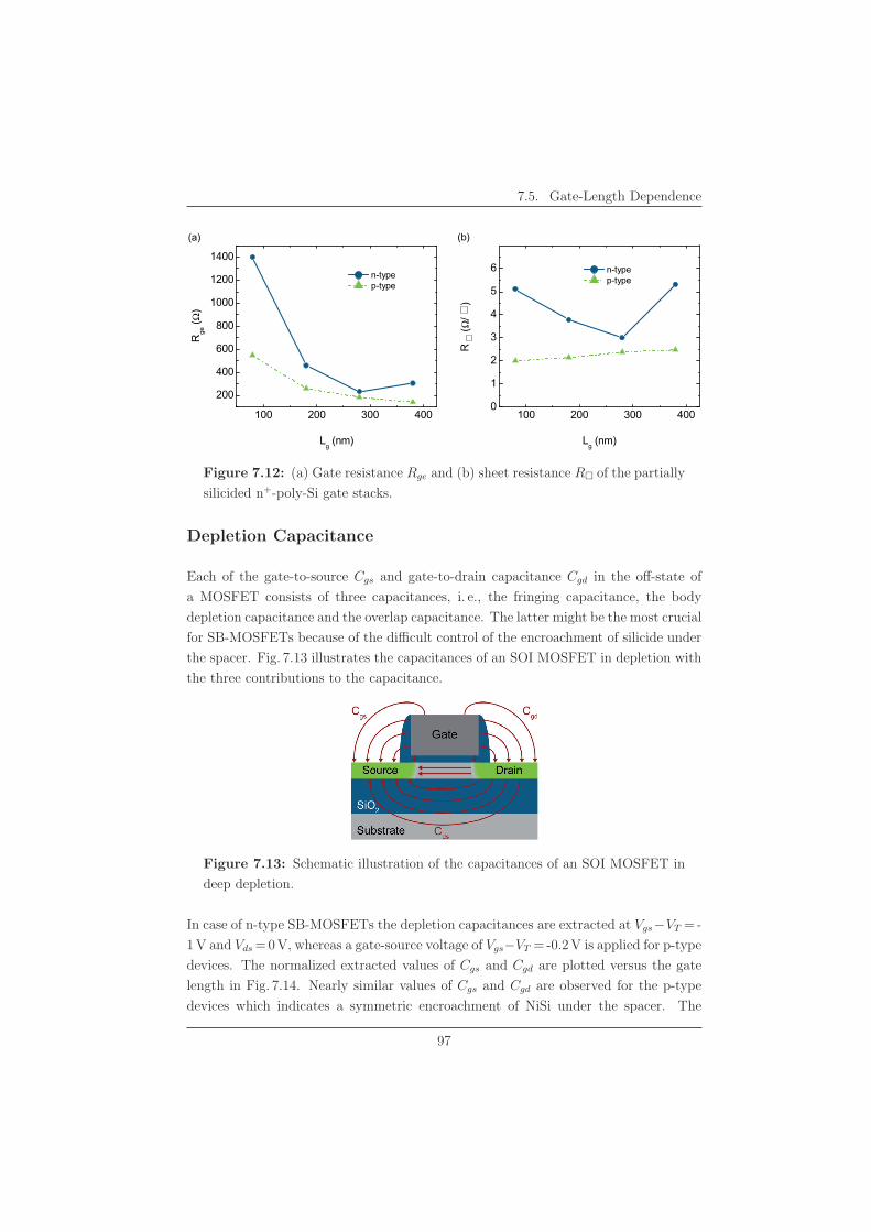
7.5. Gate-Length Dependence
100 200 300 400
200
400
600
800
1000
1200
1400
100 200 300 4000
1
2
3
4
5
6
(b)
Rge
(Ω)
Lg (nm)
n-type p-type
R
(Ω/
)
Lg (nm)
n-type p-type
(a)
Figure 7.12: (a) Gate resistance Rge and (b) sheet resistance R� of the partially
silicided n+-poly-Si gate stacks.
Depletion Capacitance
Each of the gate-to-source Cgs and gate-to-drain capacitance Cgd in the off-state of
a MOSFET consists of three capacitances, i. e., the fringing capacitance, the body
depletion capacitance and the overlap capacitance. The latter might be the most crucial
for SB-MOSFETs because of the difficult control of the encroachment of silicide under
the spacer. Fig. 7.13 illustrates the capacitances of an SOI MOSFET in depletion with
the three contributions to the capacitance.
Figure 7.13: Schematic illustration of the capacitances of an SOI MOSFET in
deep depletion.
In case of n-type SB-MOSFETs the depletion capacitances are extracted at Vgs−VT = -
1 V and Vds = 0 V, whereas a gate-source voltage of Vgs−VT = -0.2 V is applied for p-type
devices. The normalized extracted values of Cgs and Cgd are plotted versus the gate
length in Fig. 7.14. Nearly similar values of Cgs and Cgd are observed for the p-type
devices which indicates a symmetric encroachment of NiSi under the spacer. The
97
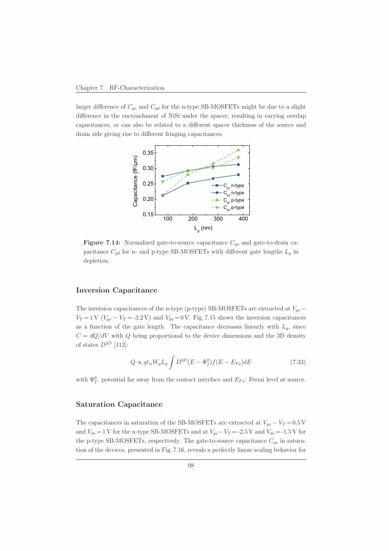
Chapter 7. RF-Characterization
larger difference of Cgs and Cgd for the n-type SB-MOSFETs might be due to a slight
difference in the encroachment of NiSi under the spacer, resulting in varying overlap
capacitances, or can also be related to a different spacer thickness of the source and
drain side giving rise to different fringing capacitances.
100 200 300 4000.15
0.20
0.25
0.30
0.35
�����������0
����
Lg (nm)
Cgs n-type Cgd n-type Cgs p-type Cgd p-type
Figure 7.14: Normalized gate-to-source capacitance Cgs and gate-to-drain ca-
pacitance Cgd for n- and p-type SB-MOSFETs with different gate lengths Lg in
depletion.
Inversion Capacitance
The inversion capacitances of the n-type (p-type) SB-MOSFETs are extracted at Vgs−VT = 1 V (Vgs − VT = -3.2 V) and Vds = 0 V. Fig. 7.15 shows the inversion capacitances
as a function of the gate length. The capacitance decreases linearly with Lg, since
C = dQ/dV with Q being proportional to the device dimensions and the 3D density
of states D3D [112]:
Q ∝ qtsiWgLg
∫D3D(E − Φ0
f )f(E − EFs)dE (7.33)
with Φ0f : potential far away from the contact interface and EFs: Fermi level at source.
Saturation Capacitance
The capacitances in saturation of the SB-MOSFETs are extracted at Vgs − VT = 0.5 V
and Vds = 1 V for the n-type SB-MOSFETs and at Vgs−VT = -2.5 V and Vds = -1.5 V for
the p-type SB-MOSFETs, respectively. The gate-to-source capacitance Cgs in satura-
tion of the devices, presented in Fig. 7.16, reveals a perfectly linear scaling behavior for
98
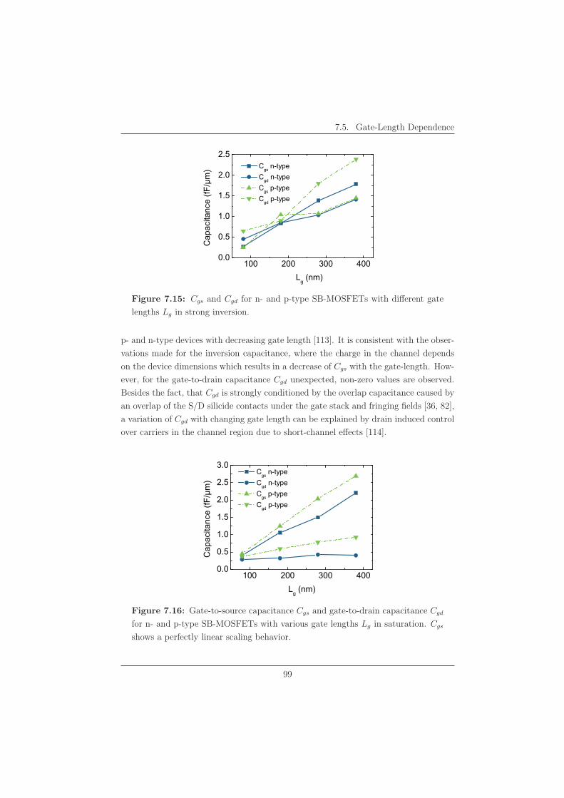
7.5. Gate-Length Dependence
100 200 300 4000.0
0.5
1.0
1.5
2.0
2.5
�����������0
����
Lg (nm)
Cgs n-type Cgd n-type Cgs p-type Cgd p-type
Figure 7.15: Cgs and Cgd for n- and p-type SB-MOSFETs with different gate
lengths Lg in strong inversion.
p- and n-type devices with decreasing gate length [113]. It is consistent with the obser-
vations made for the inversion capacitance, where the charge in the channel depends
on the device dimensions which results in a decrease of Cgs with the gate-length. How-
ever, for the gate-to-drain capacitance Cgd unexpected, non-zero values are observed.
Besides the fact, that Cgd is strongly conditioned by the overlap capacitance caused by
an overlap of the S/D silicide contacts under the gate stack and fringing fields [36, 82],
a variation of Cgd with changing gate length can be explained by drain induced control
over carriers in the channel region due to short-channel effects [114].
100 200 300 4000.0
0.5
1.0
1.5
2.0
2.5
3.0
���
������������
��
Lg (nm)
Cgs n-type Cgd n-type Cgs p-type Cgd p-type
Figure 7.16: Gate-to-source capacitance Cgs and gate-to-drain capacitance Cgd
for n- and p-type SB-MOSFETs with various gate lengths Lg in saturation. Cgs
shows a perfectly linear scaling behavior.
99
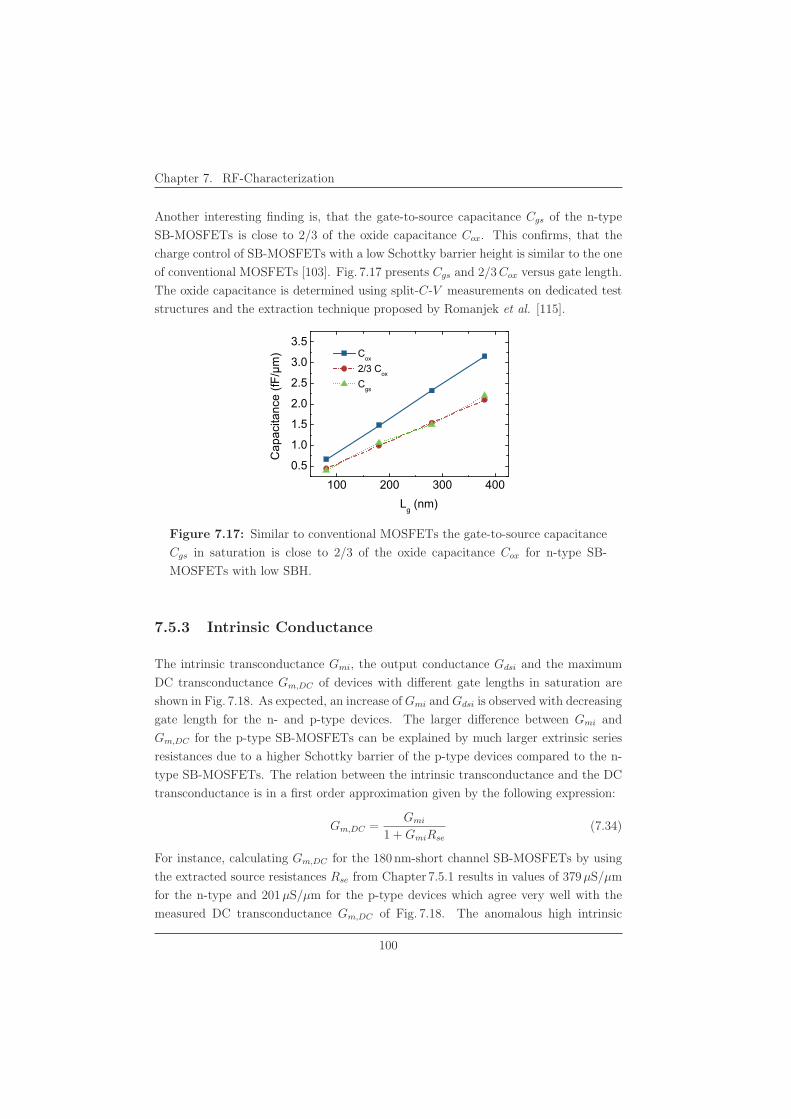
Chapter 7. RF-Characterization
Another interesting finding is, that the gate-to-source capacitance Cgs of the n-type
SB-MOSFETs is close to 2/3 of the oxide capacitance Cox. This confirms, that the
charge control of SB-MOSFETs with a low Schottky barrier height is similar to the one
of conventional MOSFETs [103]. Fig. 7.17 presents Cgs and 2/3 Cox versus gate length.
The oxide capacitance is determined using split-C-V measurements on dedicated test
structures and the extraction technique proposed by Romanjek et al. [115].
100 200 300 4000.5
1.0
1.5
2.0
2.5
3.0
3.5
�����������0
����
Lg (nm)
Cox
2/3 Cox
Cgs
Figure 7.17: Similar to conventional MOSFETs the gate-to-source capacitance
Cgs in saturation is close to 2/3 of the oxide capacitance Cox for n-type SB-
MOSFETs with low SBH.
7.5.3 Intrinsic Conductance
The intrinsic transconductance Gmi, the output conductance Gdsi and the maximum
DC transconductance Gm,DC of devices with different gate lengths in saturation are
shown in Fig. 7.18. As expected, an increase of Gmi and Gdsi is observed with decreasing
gate length for the n- and p-type devices. The larger difference between Gmi and
Gm,DC for the p-type SB-MOSFETs can be explained by much larger extrinsic series
resistances due to a higher Schottky barrier of the p-type devices compared to the n-
type SB-MOSFETs. The relation between the intrinsic transconductance and the DC
transconductance is in a first order approximation given by the following expression:
Gm,DC =Gmi
1 + GmiRse
(7.34)
For instance, calculating Gm,DC for the 180 nm-short channel SB-MOSFETs by using
the extracted source resistances Rse from Chapter 7.5.1 results in values of 379μS/μm
for the n-type and 201μS/μm for the p-type devices which agree very well with the
measured DC transconductance Gm,DC of Fig. 7.18. The anomalous high intrinsic
100
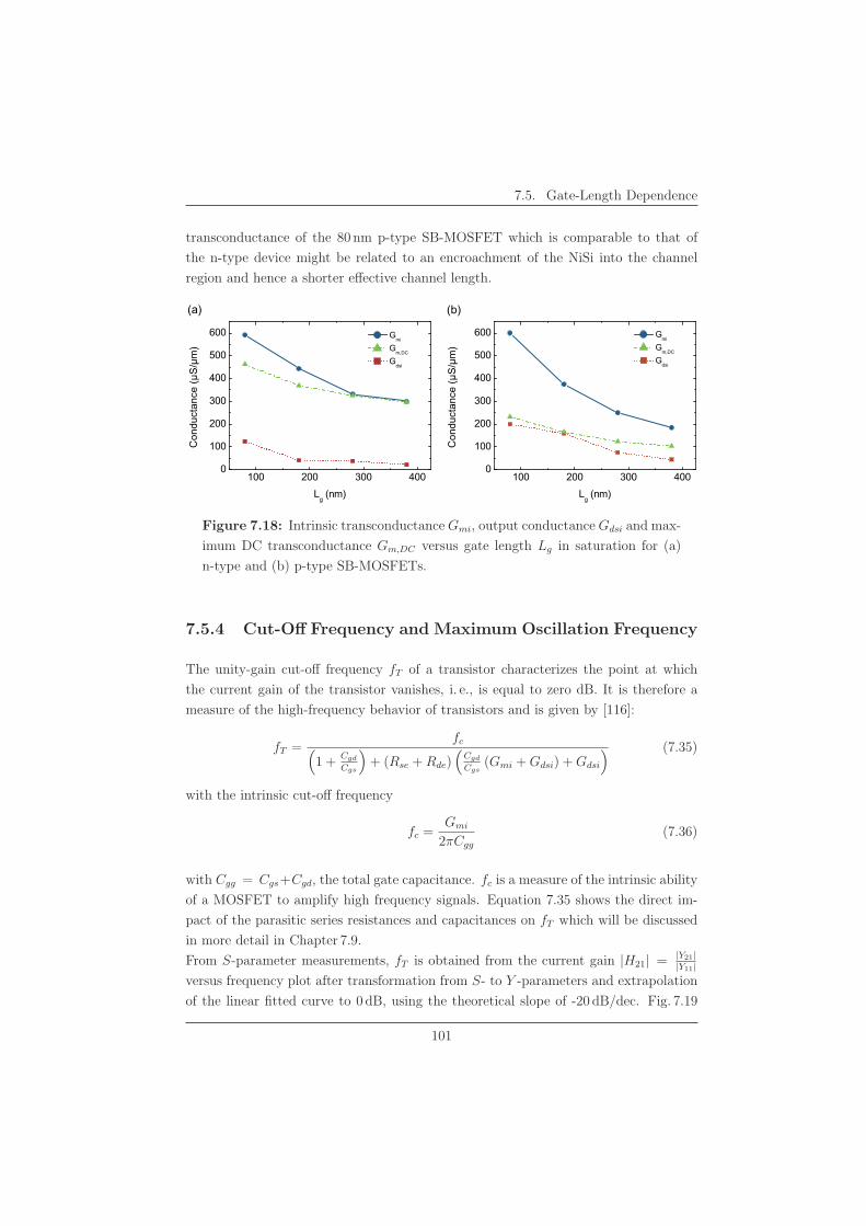
7.5. Gate-Length Dependence
transconductance of the 80 nm p-type SB-MOSFET which is comparable to that of
the n-type device might be related to an encroachment of the NiSi into the channel
region and hence a shorter effective channel length.
100 200 300 4000
100
200
300
400
500
600
100 200 300 4000
100
200
300
400
500
600
(b)
��"�������������
Lg (nm)
Gmi
Gm,DC
Gdsi
(a)
��"�������������
Lg (nm)
Gmi
Gm,DC
Gdsi
Figure 7.18: Intrinsic transconductance Gmi, output conductance Gdsi and max-
imum DC transconductance Gm,DC versus gate length Lg in saturation for (a)
n-type and (b) p-type SB-MOSFETs.
7.5.4 Cut-Off Frequency and Maximum Oscillation Frequency
The unity-gain cut-off frequency fT of a transistor characterizes the point at which
the current gain of the transistor vanishes, i. e., is equal to zero dB. It is therefore a
measure of the high-frequency behavior of transistors and is given by [116]:
fT =fc(
1 +Cgd
Cgs
)+ (Rse + Rde)
(Cgd
Cgs(Gmi + Gdsi) + Gdsi
) (7.35)
with the intrinsic cut-off frequency
fc =Gmi
2πCgg
(7.36)
with Cgg = Cgs+Cgd, the total gate capacitance. fc is a measure of the intrinsic ability
of a MOSFET to amplify high frequency signals. Equation 7.35 shows the direct im-
pact of the parasitic series resistances and capacitances on fT which will be discussed
in more detail in Chapter 7.9.
From S-parameter measurements, fT is obtained from the current gain |H21| = |Y21||Y11|
versus frequency plot after transformation from S- to Y -parameters and extrapolation
of the linear fitted curve to 0 dB, using the theoretical slope of -20 dB/dec. Fig. 7.19
101
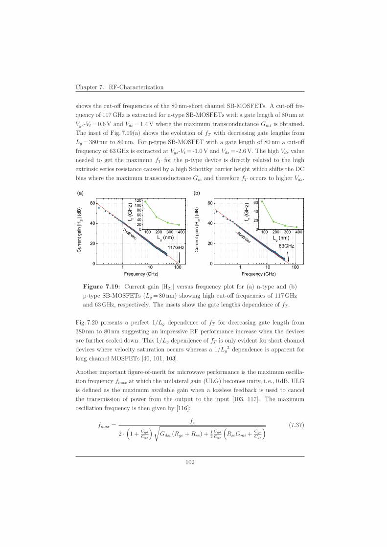
Chapter 7. RF-Characterization
shows the cut-off frequencies of the 80 nm-short channel SB-MOSFETs. A cut-off fre-
quency of 117 GHz is extracted for n-type SB-MOSFETs with a gate length of 80 nm at
Vgs-Vt = 0.6 V and Vds = 1.4 V where the maximum transconductance Gmi is obtained.
The inset of Fig. 7.19(a) shows the evolution of fT with decreasing gate lengths from
Lg = 380 nm to 80 nm. For p-type SB-MOSFET with a gate length of 80 nm a cut-off
frequency of 63 GHz is extracted at Vgs-Vt = -1.0 V and Vds = -2.6 V. The high Vds value
needed to get the maximum fT for the p-type device is directly related to the high
extrinsic series resistance caused by a high Schottky barrier height which shifts the DC
bias where the maximum transconductance Gm and therefore fT occurs to higher Vds.
1 10 1000
20
40
60
100 200 300 400020406080
100120
1 10 1000
20
40
60
100 200 300 4000
20
40
60
(b)
117GHz
Cur
rent
gai
n |H
21| (
dB)
Frequency (GHz)
-20dB/dec
(a)
f T (G
Hz)
Lg (nm)
C
urre
nt g
ain
|H21
| (dB
)
Frequency (GHz)
63GHz
-20dB/decf T (
GH
z)L
g (nm)
Figure 7.19: Current gain |H21| versus frequency plot for (a) n-type and (b)
p-type SB-MOSFETs (Lg = 80 nm) showing high cut-off frequencies of 117 GHz
and 63 GHz, respectively. The insets show the gate lengths dependence of fT .
Fig. 7.20 presents a perfect 1/Lg dependence of fT for decreasing gate length from
380 nm to 80 nm suggesting an impressive RF performance increase when the devices
are further scaled down. This 1/Lg dependence of fT is only evident for short-channel
devices where velocity saturation occurs whereas a 1/Lg2 dependence is apparent for
long-channel MOSFETs [40, 101, 103].
Another important figure-of-merit for microwave performance is the maximum oscilla-
tion frequency fmax at which the unilateral gain (ULG) becomes unity, i. e., 0 dB. ULG
is defined as the maximum available gain when a lossless feedback is used to cancel
the transmission of power from the output to the input [103, 117]. The maximum
oscillation frequency is then given by [116]:
fmax =fc
2 ·(1 +
Cgd
Cgs
) √Gdsi (Rge + Rse) + 1
2
Cgd
Cgs
(RseGmi +
Cgd
Cgs
) (7.37)
102
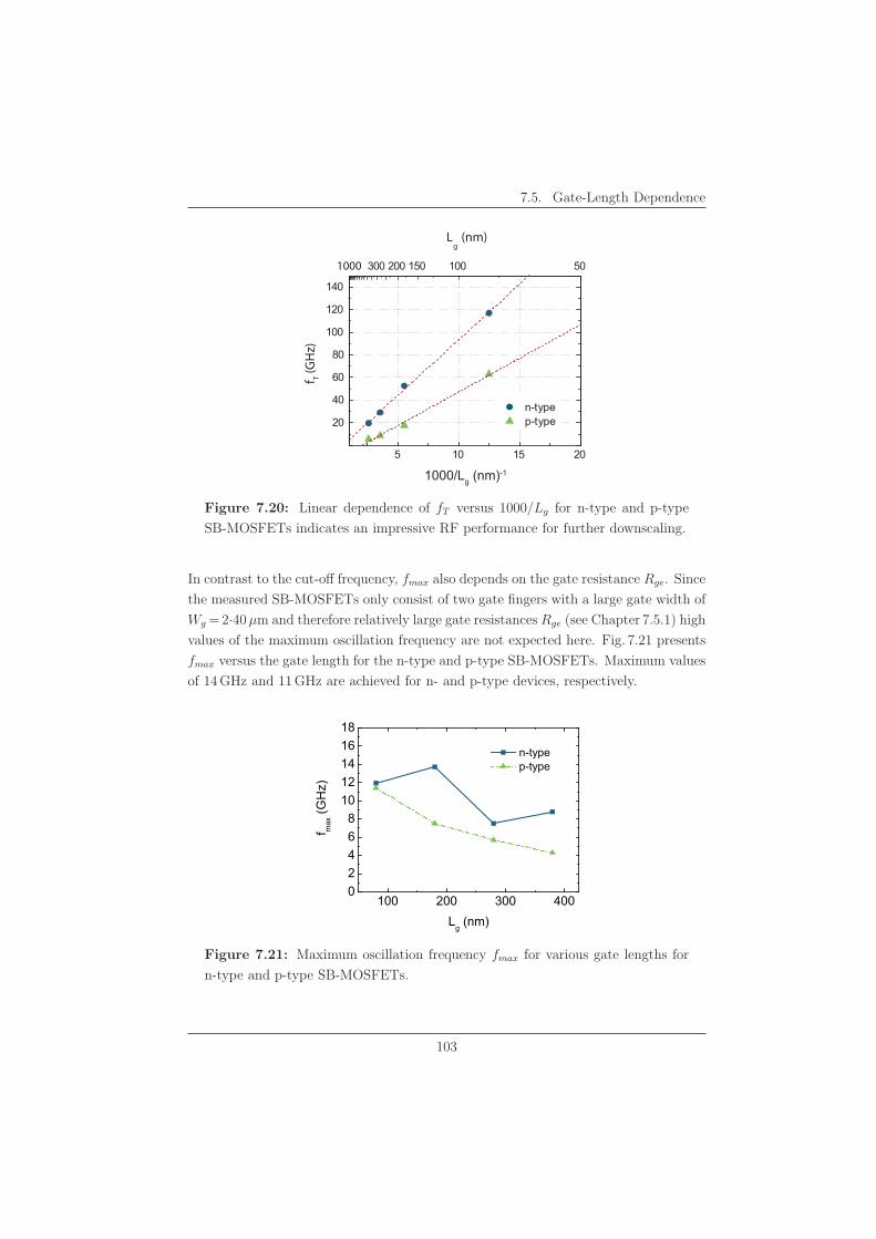
7.5. Gate-Length Dependence
5 10 15 20
20
40
60
80
100
120
140
n-type p-type
f T (GH
z)
1000/Lg (nm)-1
1000 300 200 150 100 50
Lg (nm)
Figure 7.20: Linear dependence of fT versus 1000/Lg for n-type and p-type
SB-MOSFETs indicates an impressive RF performance for further downscaling.
In contrast to the cut-off frequency, fmax also depends on the gate resistance Rge. Since
the measured SB-MOSFETs only consist of two gate fingers with a large gate width of
Wg = 2·40 μm and therefore relatively large gate resistances Rge (see Chapter 7.5.1) high
values of the maximum oscillation frequency are not expected here. Fig. 7.21 presents
fmax versus the gate length for the n-type and p-type SB-MOSFETs. Maximum values
of 14 GHz and 11 GHz are achieved for n- and p-type devices, respectively.
100 200 300 40002468
1012141618
f max
(GH
z)
Lg (nm)
n-type p-type
Figure 7.21: Maximum oscillation frequency fmax for various gate lengths for
n-type and p-type SB-MOSFETs.
103
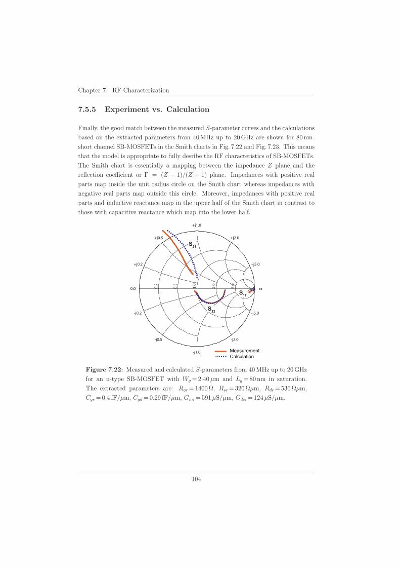
Chapter 7. RF-Characterization
7.5.5 Experiment vs. Calculation
Finally, the good match between the measured S-parameter curves and the calculations
based on the extracted parameters from 40 MHz up to 20 GHz are shown for 80 nm-
short channel SB-MOSFETs in the Smith charts in Fig. 7.22 and Fig. 7.23. This means
that the model is appropriate to fully desribe the RF characteristics of SB-MOSFETs.
The Smith chart is essentially a mapping between the impedance Z plane and the
reflection coefficient or Γ = (Z − 1)/(Z + 1) plane. Impedances with positive real
parts map inside the unit radius circle on the Smith chart whereas impedances with
negative real parts map outside this circle. Moreover, impedances with positive real
parts and inductive reactance map in the upper half of the Smith chart in contrast to
those with capacitive reactance which map into the lower half.
0.2
0.5
1.0
2.0
5.0
+j0.2
-j0.2
+j0.5
-j0.5
+j1.0
-j1.0
+j2.0
-j2.0
+j5.0
-j5.0
0.0 ∞S11
S21
S22
MeasurementCalculation
Figure 7.22: Measured and calculated S-parameters from 40 MHz up to 20 GHz
for an n-type SB-MOSFET with Wg = 2·40 μm and Lg = 80 nm in saturation.
The extracted parameters are: Rge = 1400 Ω, Rse = 320 Ωμm, Rde = 536 Ωμm,
Cgs = 0.4 fF/μm, Cgd = 0.29 fF/μm, Gmi = 591μS/μm, Gdsi = 124μS/μm.
104
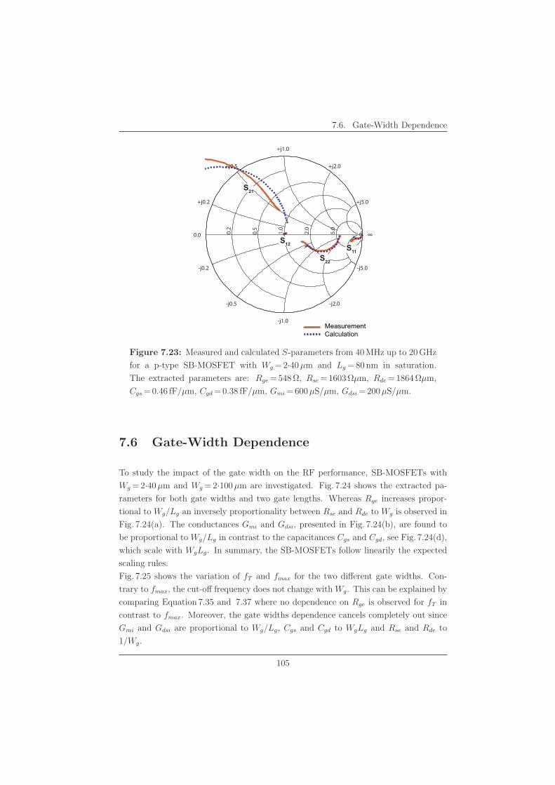
7.6. Gate-Width Dependence
∞0.2
0.5
1.0
2.0
5.0
+j0.2
-j0.2
+j0.5
-j0.5
+j1.0
-j1.0
+j2.0
-j2.0
+j5.0
-j5.0
0.0
S21
S12
S22S11
MeasurementCalculation
Figure 7.23: Measured and calculated S-parameters from 40 MHz up to 20 GHz
for a p-type SB-MOSFET with Wg = 2·40 μm and Lg = 80 nm in saturation.
The extracted parameters are: Rge = 548 Ω, Rse = 1603 Ωμm, Rde = 1864 Ωμm,
Cgs = 0.46 fF/μm, Cgd = 0.38 fF/μm, Gmi = 600μS/μm, Gdsi = 200μS/μm.
7.6 Gate-Width Dependence
To study the impact of the gate width on the RF performance, SB-MOSFETs with
Wg = 2·40μm and Wg = 2·100μm are investigated. Fig. 7.24 shows the extracted pa-
rameters for both gate widths and two gate lengths. Whereas Rge increases propor-
tional to Wg/Lg an inversely proportionality between Rse and Rde to Wg is observed in
Fig. 7.24(a). The conductances Gmi and Gdsi, presented in Fig. 7.24(b), are found to
be proportional to Wg/Lg in contrast to the capacitances Cgs and Cgd, see Fig. 7.24(d),
which scale with WgLg. In summary, the SB-MOSFETs follow linearily the expected
scaling rules.
Fig. 7.25 shows the variation of fT and fmax for the two different gate widths. Con-
trary to fmax, the cut-off frequency does not change with Wg. This can be explained by
comparing Equation 7.35 and 7.37 where no dependence on Rge is observed for fT in
contrast to fmax. Moreover, the gate widths dependence cancels completely out since
Gmi and Gdsi are proportional to Wg/Lg, Cgs and Cgd to WgLg and Rse and Rde to
1/Wg.
105
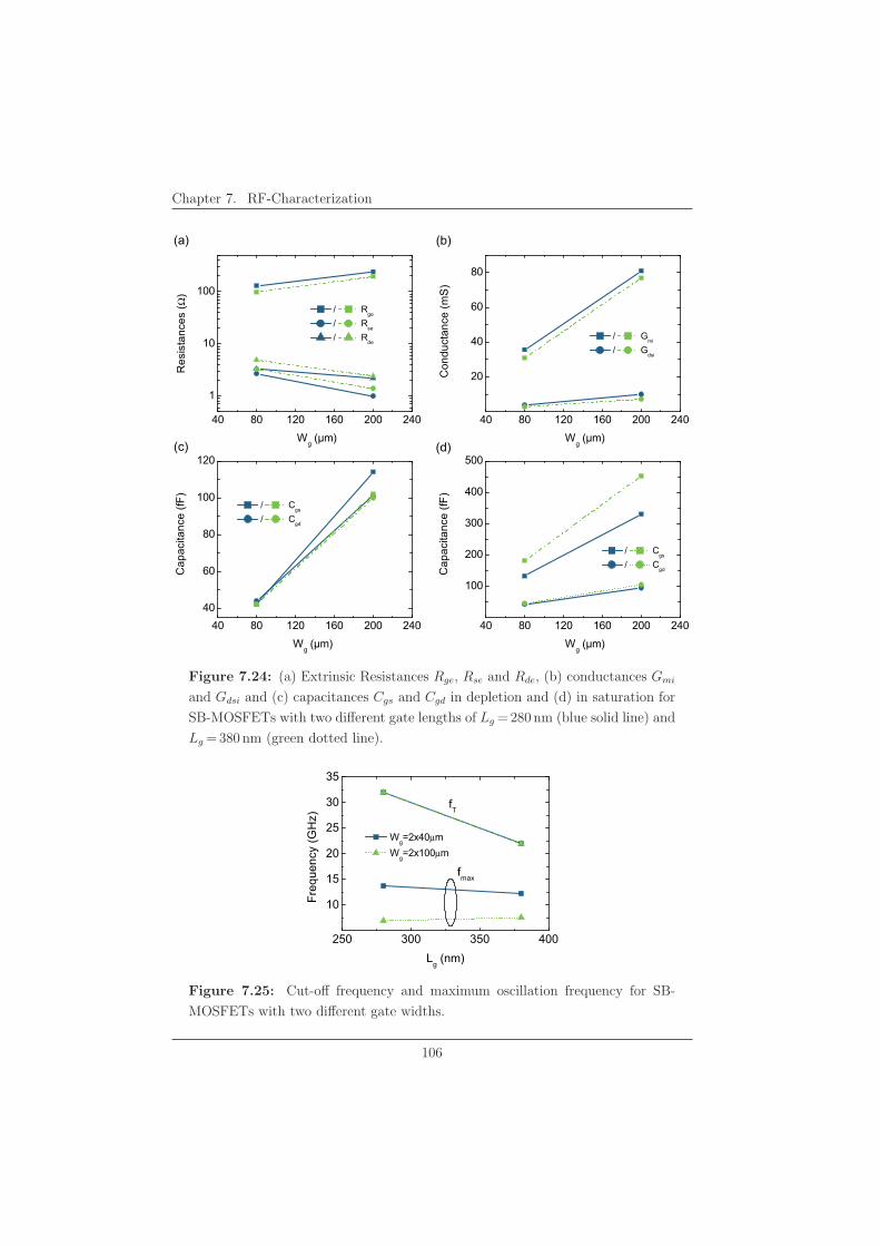
Chapter 7. RF-Characterization
40 80 120 160 200 24040
60
80
100
120
40 80 120 160 200 240
1
10
100
40 80 120 160 200 240
20
40
60
80
40 80 120 160 200 240
100
200
300
400
500
���
Cap
acita
nce
(fF)
� � ���
� � � �
� � � � �
���
Res
ista
nces
(Ω)
� � ���
� � � � �
� � � � �
� � � ���
������
Con
duct
ance
(mS
)�
� ���
� � � !�
� � � !� �
Cap
acita
nce
(fF)
� � ���
� � � �
� � � � �
Figure 7.24: (a) Extrinsic Resistances Rge, Rse and Rde, (b) conductances Gmi
and Gdsi and (c) capacitances Cgs and Cgd in depletion and (d) in saturation for
SB-MOSFETs with two different gate lengths of Lg = 280 nm (blue solid line) and
Lg = 380 nm (green dotted line).
250 300 350 400
10
15
20
25
30
35
fT
Freq
uenc
y (G
Hz)
Lg (nm)
Wg=2x40μm Wg=2x100μm
fmax
Figure 7.25: Cut-off frequency and maximum oscillation frequency for SB-
MOSFETs with two different gate widths.
106
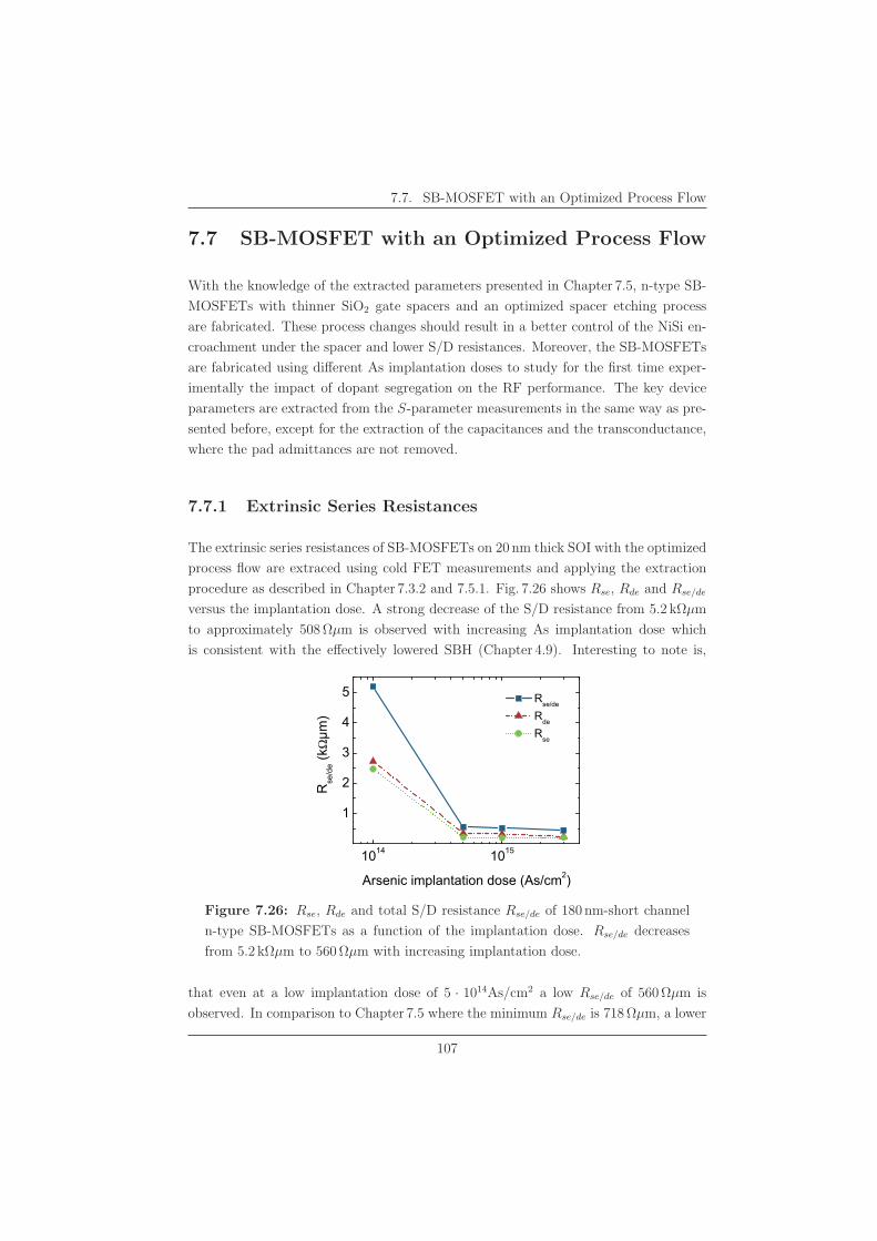
7.7. SB-MOSFET with an Optimized Process Flow
7.7 SB-MOSFET with an Optimized Process Flow
With the knowledge of the extracted parameters presented in Chapter 7.5, n-type SB-
MOSFETs with thinner SiO2 gate spacers and an optimized spacer etching process
are fabricated. These process changes should result in a better control of the NiSi en-
croachment under the spacer and lower S/D resistances. Moreover, the SB-MOSFETs
are fabricated using different As implantation doses to study for the first time exper-
imentally the impact of dopant segregation on the RF performance. The key device
parameters are extracted from the S-parameter measurements in the same way as pre-
sented before, except for the extraction of the capacitances and the transconductance,
where the pad admittances are not removed.
7.7.1 Extrinsic Series Resistances
The extrinsic series resistances of SB-MOSFETs on 20 nm thick SOI with the optimized
process flow are extraced using cold FET measurements and applying the extraction
procedure as described in Chapter 7.3.2 and 7.5.1. Fig. 7.26 shows Rse, Rde and Rse/de
versus the implantation dose. A strong decrease of the S/D resistance from 5.2 kΩμm
to approximately 508 Ωμm is observed with increasing As implantation dose which
is consistent with the effectively lowered SBH (Chapter 4.9). Interesting to note is,
1014 1015
1
2
3
4
5 Rse/de
Rde
Rse
� ������Ω
��
Arsenic implantation dose (As/cm2)
Figure 7.26: Rse, Rde and total S/D resistance Rse/de of 180 nm-short channel
n-type SB-MOSFETs as a function of the implantation dose. Rse/de decreases
from 5.2 kΩμm to 560 Ωμm with increasing implantation dose.
that even at a low implantation dose of 5 · 1014As/cm2 a low Rse/de of 560 Ωμm is
observed. In comparison to Chapter 7.5 where the minimum Rse/de is 718 Ωμm, a lower
107
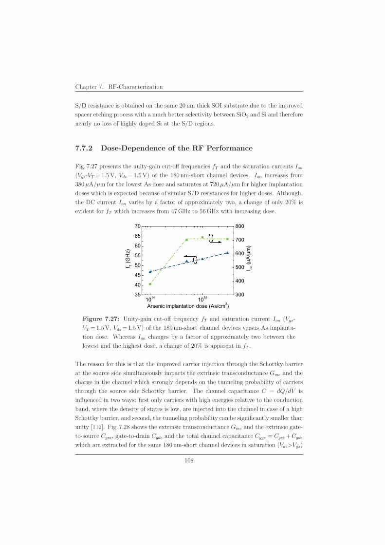
Chapter 7. RF-Characterization
S/D resistance is obtained on the same 20 nm thick SOI substrate due to the improved
spacer etching process with a much better selectivity between SiO2 and Si and therefore
nearly no loss of highly doped Si at the S/D regions.
7.7.2 Dose-Dependence of the RF Performance
Fig. 7.27 presents the unity-gain cut-off frequencies fT and the saturation currents Ion
(Vgs-VT = 1.5 V, Vds = 1.5 V) of the 180 nm-short channel devices. Ion increases from
380μA/μm for the lowest As dose and saturates at 720μA/μm for higher implantation
doses which is expected because of similar S/D resistances for higher doses. Although,
the DC current Ion varies by a factor of approximately two, a change of only 20% is
evident for fT which increases from 47 GHz to 56 GHz with increasing dose.
1014 101535
40
45
50
55
60
65
70
0 ��123�
Arsenic implantation dose (As/cm2)
300
400
500
600
700
800
� �����
����
Figure 7.27: Unity-gain cut-off frequency fT and saturation current Ion (Vgs-
VT = 1.5 V, Vds = 1.5 V) of the 180 nm-short channel devices versus As implanta-
tion dose. Whereas Ion changes by a factor of approximately two between the
lowest and the highest dose, a change of 20% is apparent in fT .
The reason for this is that the improved carrier injection through the Schottky barrier
at the source side simultaneously impacts the extrinsic transconductance Gme and the
charge in the channel which strongly depends on the tunneling probability of carriers
through the source side Schottky barrier. The channel capacitance C = dQ/dV is
influenced in two ways: first only carriers with high energies relative to the conduction
band, where the density of states is low, are injected into the channel in case of a high
Schottky barrier, and second, the tunneling probability can be significantly smaller than
unity [112]. Fig. 7.28 shows the extrinsic transconductance Gme and the extrinsic gate-
to-source Cgse, gate-to-drain Cgde and the total channel capacitance Cgge = Cgse +Cgde
which are extracted for the same 180 nm-short channel devices in saturation (Vds>Vgs)
108
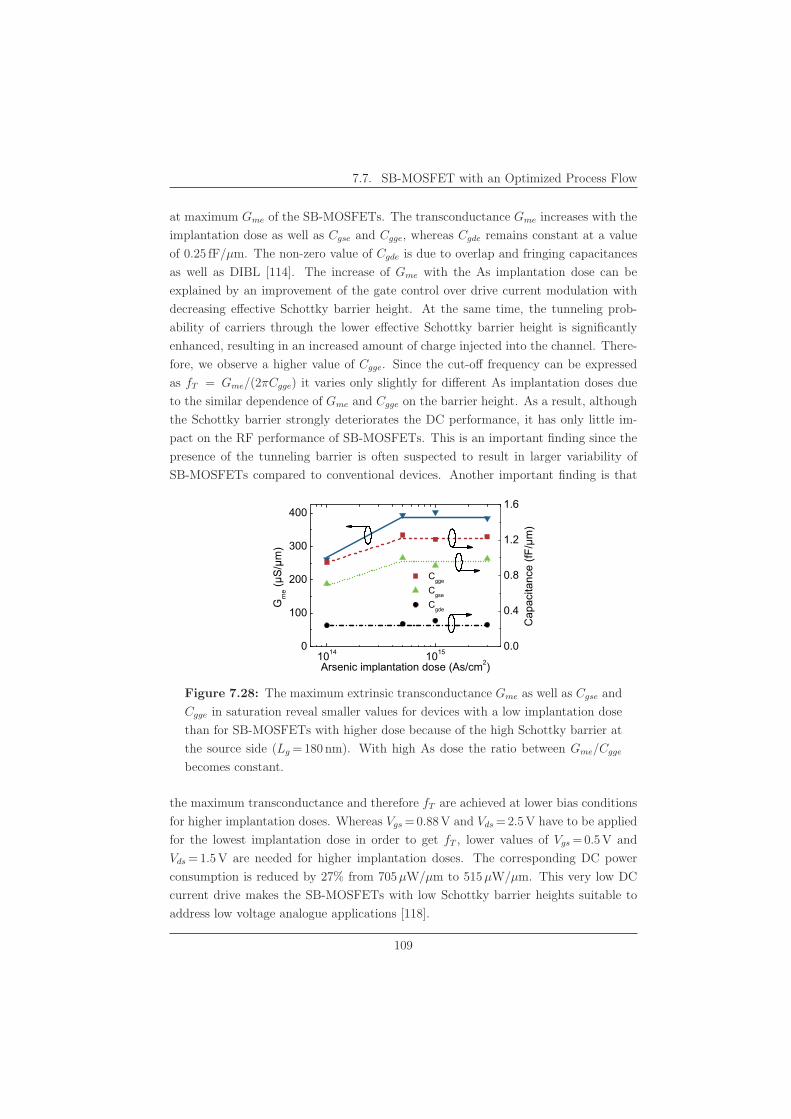
7.7. SB-MOSFET with an Optimized Process Flow
at maximum Gme of the SB-MOSFETs. The transconductance Gme increases with the
implantation dose as well as Cgse and Cgge, whereas Cgde remains constant at a value
of 0.25 fF/μm. The non-zero value of Cgde is due to overlap and fringing capacitances
as well as DIBL [114]. The increase of Gme with the As implantation dose can be
explained by an improvement of the gate control over drive current modulation with
decreasing effective Schottky barrier height. At the same time, the tunneling prob-
ability of carriers through the lower effective Schottky barrier height is significantly
enhanced, resulting in an increased amount of charge injected into the channel. There-
fore, we observe a higher value of Cgge. Since the cut-off frequency can be expressed
as fT = Gme/(2πCgge) it varies only slightly for different As implantation doses due
to the similar dependence of Gme and Cgge on the barrier height. As a result, although
the Schottky barrier strongly deteriorates the DC performance, it has only little im-
pact on the RF performance of SB-MOSFETs. This is an important finding since the
presence of the tunneling barrier is often suspected to result in larger variability of
SB-MOSFETs compared to conventional devices. Another important finding is that
1014 10150
100
200
300
400
����� ��
Arsenic implantation dose (As/cm2)
0.0
0.4
0.8
1.2
1.6
Cgge
Cgse
Cgde
�!������������"#��
Figure 7.28: The maximum extrinsic transconductance Gme as well as Cgse and
Cgge in saturation reveal smaller values for devices with a low implantation dose
than for SB-MOSFETs with higher dose because of the high Schottky barrier at
the source side (Lg = 180 nm). With high As dose the ratio between Gme/Cgge
becomes constant.
the maximum transconductance and therefore fT are achieved at lower bias conditions
for higher implantation doses. Whereas Vgs = 0.88 V and Vds = 2.5 V have to be applied
for the lowest implantation dose in order to get fT , lower values of Vgs = 0.5 V and
Vds = 1.5 V are needed for higher implantation doses. The corresponding DC power
consumption is reduced by 27% from 705μW/μm to 515μW/μm. This very low DC
current drive makes the SB-MOSFETs with low Schottky barrier heights suitable to
address low voltage analogue applications [118].
109
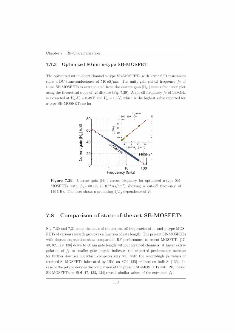
Chapter 7. RF-Characterization
7.7.3 Optimized 80 nm n-type SB-MOSFET
The optimized 80 nm-short channel n-type SB-MOSFETs with lower S/D resistances
show a DC transconductance of 510μS/μm. The unity-gain cut-off frequency fT of
these SB-MOSFETs is extrapolated from the current gain |H21| versus frequency plot
using the theoretical slope of -20 dB/dec (Fig. 7.29). A cut-off frequency fT of 140 GHz
is extracted at Vgs-VT = 0.38 V and Vds = 1.6 V, which is the highest value reported for
n-type SB-MOSFETs so far.
1 10 1000
20
40
60
80
Cur
rent
gai
n |H
21| (
dB)
Frequency (GHz)
-20dB/dec140GHz
1000/Lg (nm -1)
300 150 100 50 Lg (nm)
4 8 12 16
40
80
120
160
(GH
z)f T
Figure 7.29: Current gain |H21| versus frequency for optimized n-type SB-
MOSFETs with Lg = 80 nm (3·1015 As/cm2) showing a cut-off frequency of
140 GHz. The inset shows a promising 1/Lg dependence of fT .
7.8 Comparison of state-of-the-art SB-MOSFETs
Fig. 7.30 and 7.31 show the state-of-the-art cut-off frequencies of n- and p-type MOS-
FETs of various research groups as a function of gate length. The present SB-MOSFETs
with dopant segregation show comparable RF performance to recent MOSFETs [17,
40, 82, 119–136] down to 80 nm gate length without strained channels. A linear extra-
polation of fT to smaller gate lengths indicates the expected performance increase
for further downscaling which competes very well with the record-high fT values of
strained-Si MOSFETs fabricated by IBM on SOI [135] or Intel on bulk Si [136]. In
case of the p-type devices the comparison of the present SB-MOSFETs with PtSi based
SB-MOSFETs on SOI [17, 133, 134] reveals similar values of the extracted fT .
110
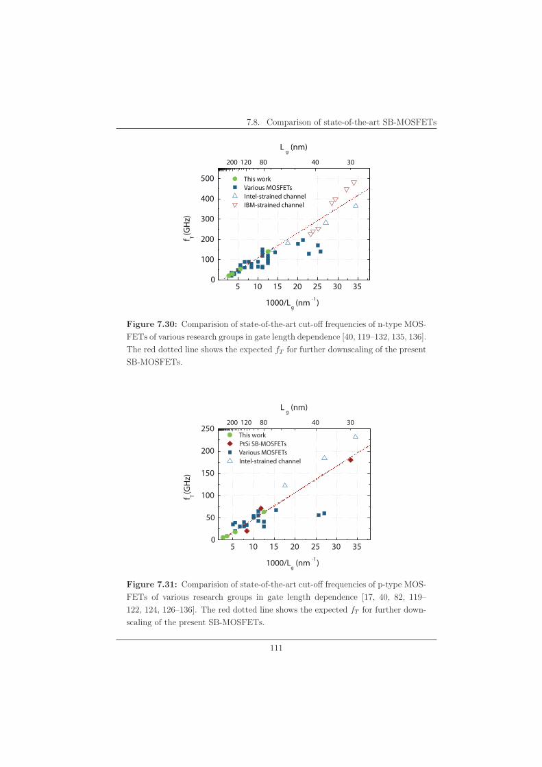
7.8. Comparison of state-of-the-art SB-MOSFETs
5 10 15 20 25 30 350
100
200
300
400
500 This work Various MOSFETs Intel-strained channel IBM-strained channel
f T (GH
z)
1000/Lg (nm -1)
200 120 80 40 30
Lg (nm)
Figure 7.30: Comparision of state-of-the-art cut-off frequencies of n-type MOS-
FETs of various research groups in gate length dependence [40, 119–132, 135, 136].
The red dotted line shows the expected fT for further downscaling of the present
SB-MOSFETs.
5 10 15 20 25 30 350
50
100
150
200
250 This work PtSi SB-MOSFETs Various MOSFETs Intel-strained channel
f T (GH
z)
1000/Lg (nm -1)
200 120 80 40 30
Lg (nm)
Figure 7.31: Comparision of state-of-the-art cut-off frequencies of p-type MOS-
FETs of various research groups in gate length dependence [17, 40, 82, 119–
122, 124, 126–136]. The red dotted line shows the expected fT for further down-
scaling of the present SB-MOSFETs.
111
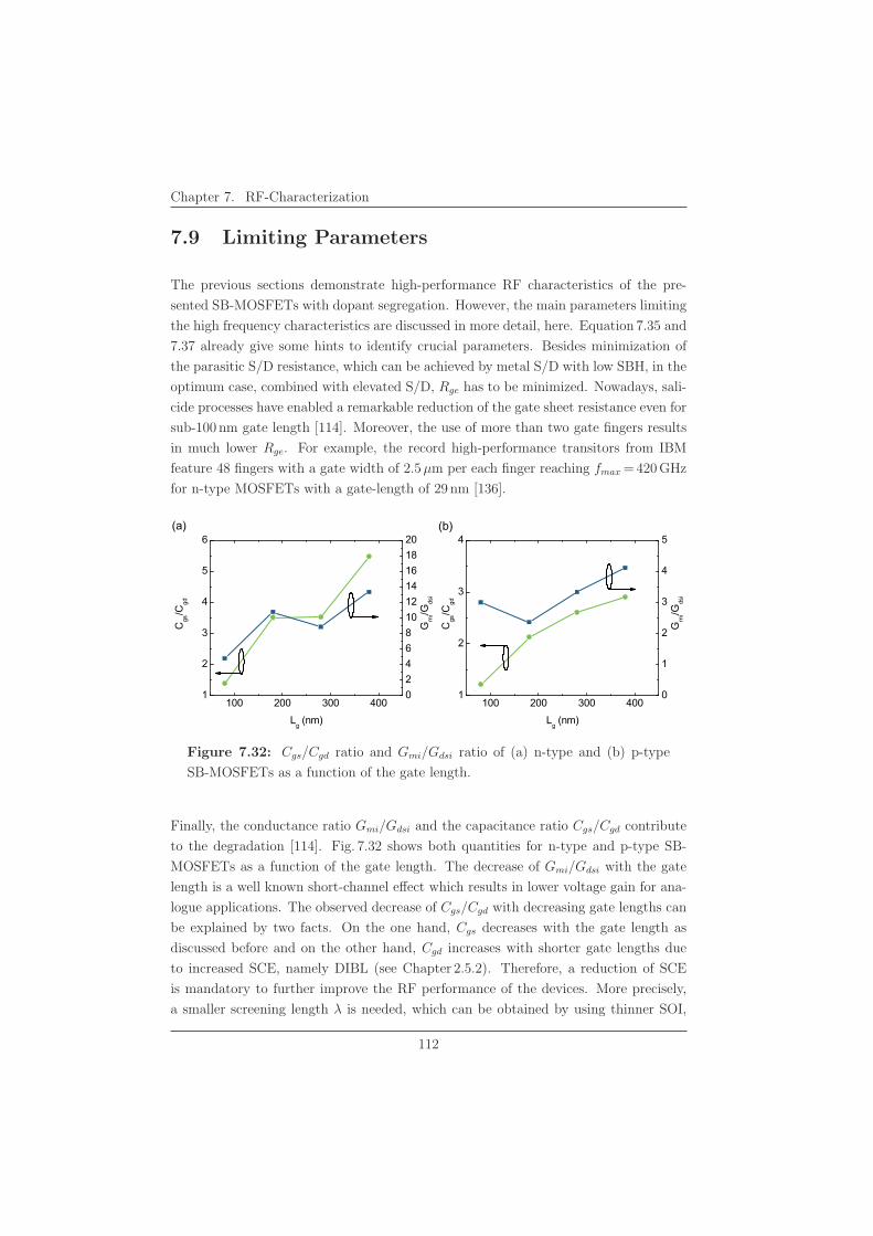
Chapter 7. RF-Characterization
7.9 Limiting Parameters
The previous sections demonstrate high-performance RF characteristics of the pre-
sented SB-MOSFETs with dopant segregation. However, the main parameters limiting
the high frequency characteristics are discussed in more detail, here. Equation 7.35 and
7.37 already give some hints to identify crucial parameters. Besides minimization of
the parasitic S/D resistance, which can be achieved by metal S/D with low SBH, in the
optimum case, combined with elevated S/D, Rge has to be minimized. Nowadays, sali-
cide processes have enabled a remarkable reduction of the gate sheet resistance even for
sub-100 nm gate length [114]. Moreover, the use of more than two gate fingers results
in much lower Rge. For example, the record high-performance transitors from IBM
feature 48 fingers with a gate width of 2.5μm per each finger reaching fmax = 420 GHz
for n-type MOSFETs with a gate-length of 29 nm [136].
100 200 300 4001
2
3
4
5
6
100 200 300 4001
2
3
4(b)
Cgs
/Cgd
Lg (nm)
(a)
02468101214161820
Gm
i/Gds
i
Cgs
/Cgd
Lg (nm)
0
1
2
3
4
5
Gm
i/Gds
i
Figure 7.32: Cgs/Cgd ratio and Gmi/Gdsi ratio of (a) n-type and (b) p-type
SB-MOSFETs as a function of the gate length.
Finally, the conductance ratio Gmi/Gdsi and the capacitance ratio Cgs/Cgd contribute
to the degradation [114]. Fig. 7.32 shows both quantities for n-type and p-type SB-
MOSFETs as a function of the gate length. The decrease of Gmi/Gdsi with the gate
length is a well known short-channel effect which results in lower voltage gain for ana-
logue applications. The observed decrease of Cgs/Cgd with decreasing gate lengths can
be explained by two facts. On the one hand, Cgs decreases with the gate length as
discussed before and on the other hand, Cgd increases with shorter gate lengths due
to increased SCE, namely DIBL (see Chapter 2.5.2). Therefore, a reduction of SCE
is mandatory to further improve the RF performance of the devices. More precisely,
a smaller screening length λ is needed, which can be obtained by using thinner SOI,
112
7.10. Summary
thinner gate oxides or even better high-κ gate dielectrics [137]. Moreover, new device
concepts like nanowires or FinFETs which provide better electrostatics than planar
devices [46] emerge as promising novel device structures to solve SCE problems. How-
ever, critical device parameters like parasitic resistances and capacitances which are
arising for the new architectures will become a future challenge [138–140].
7.10 Summary
A detailed investigation of radio-frequency properties of n- and p-type NiSi S/D SB-
MOSFETs with dopant segregation is presented. The extrinsic and intrinsic device
parameters which are extracted from small-signal parameters in dependence of the de-
vice dimensions provide a deep physical insight into the behavior of SB-MOSFETs.
A perfectly linear scaling is observed for devices with gate lengths from 380 nm down
to 80 nm with cut-off frequencies of 117 GHz for n-type and 63 GHz for p-type SB-
MOSFETs.
A study of the implantation dose dependence is carried out on n-type SB-MOSFETs
which are fabricated using an improved process flow with less loss of highly dopded Si
during spacer etching and better control of the NiSi encroachment due to thinner spac-
ers. By this, the S/D resistance is improved by 30% and cut-off frequencies as high as
140 GHz are obtained. The RF study of dopant segregated n-type SB-MOSFETs with
varying implantation doses, i. e., different Schottky barrier heights, reveals a lowering
of the S/D resistances by a factor of 10 when the dose is increased from 1 ·1014 As/cm2
to 3 · 1015 As/cm2. Although, the DC characteristics are strongly improved by a factor
of two in the on-current between the lowest and the highest dose, fT increases only by
20%. This smaller impact of the Schottky barrier height on the cut-off frequency which
is given by fT = Gme/(2πCgge) can be explained by a similar behavior of Gme and Cgge
for the chosen As doses which could be revealed by the extraction of the small-signal
equivalent circuit parameters.
A comparison of the present SB-MOSFETs with state-of-the-art MOSFETs shows the
superior RF performance which is comparable to various devices with the same gate
lengths and indicates an impressive increase of fT for further downscaling.
Finally, RF performance limiting parameters are discussed and besides the extrinsic
series resistances and overlap capacitances, short-channel effects are found to be crucial
since they result in a decrease of the Cgs/Cgd ratio as well as Gmi/Gdsi.
113
Chapter 7. RF-Characterization
114
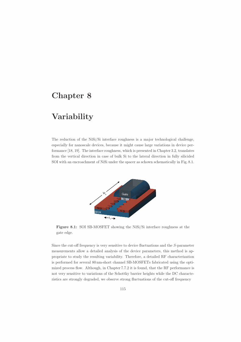
Chapter 8
Variability
The reduction of the NiSi/Si interface roughness is a major technological challenge,
especially for nanoscale devices, because it might cause large variations in device per-
formance [18, 19]. The interface roughness, which is presented in Chapter 3.2, translates
from the vertical direction in case of bulk Si to the lateral direction in fully silicided
SOI with an encroachment of NiSi under the spacer as schown schematically in Fig. 8.1.
Figure 8.1: SOI SB-MOSFET showing the NiSi/Si interface roughness at the
gate edge.
Since the cut-off frequency is very sensitive to device fluctuations and the S-parameter
measurements allow a detailed analysis of the device parameters, this method is ap-
propriate to study the resulting variability. Therefore, a detailed RF characterization
is performed for several 80 nm-short channel SB-MOSFETs fabricated using the opti-
mized process flow. Although, in Chapter 7.7.2 it is found, that the RF performance is
not very sensitive to variations of the Schottky barrier heights while the DC characte-
ristics are strongly degraded, we observe strong fluctuations of the cut-off frequency
115
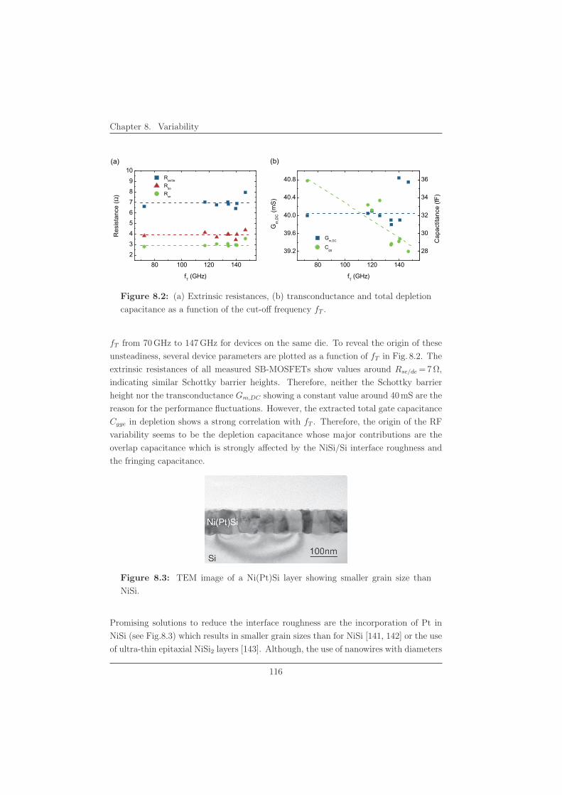
Chapter 8. Variability
80 100 120 1402
3
4
56
7
8
9
10
80 100 120 140
39.2
39.6
40.0
40.4
40.8
(a) (b)
Rse/de
Rde
Rse
Res
ista
nce
(Ω)
fT (GHz)
Gm,DC
Gm
,DC (m
S)
fT (GHz)
28
30
32
34
36
Cgg
Cap
actit
ance
(fF)
Figure 8.2: (a) Extrinsic resistances, (b) transconductance and total depletion
capacitance as a function of the cut-off frequency fT .
fT from 70 GHz to 147 GHz for devices on the same die. To reveal the origin of these
unsteadiness, several device parameters are plotted as a function of fT in Fig. 8.2. The
extrinsic resistances of all measured SB-MOSFETs show values around Rse/de = 7 Ω,
indicating similar Schottky barrier heights. Therefore, neither the Schottky barrier
height nor the transconductance Gm,DC showing a constant value around 40 mS are the
reason for the performance fluctuations. However, the extracted total gate capacitance
Cgge in depletion shows a strong correlation with fT . Therefore, the origin of the RF
variability seems to be the depletion capacitance whose major contributions are the
overlap capacitance which is strongly affected by the NiSi/Si interface roughness and
the fringing capacitance.
Figure 8.3: TEM image of a Ni(Pt)Si layer showing smaller grain size than
NiSi.
Promising solutions to reduce the interface roughness are the incorporation of Pt in
NiSi (see Fig.8.3) which results in smaller grain sizes than for NiSi [141, 142] or the use
of ultra-thin epitaxial NiSi2 layers [143]. Although, the use of nanowires with diameters
116
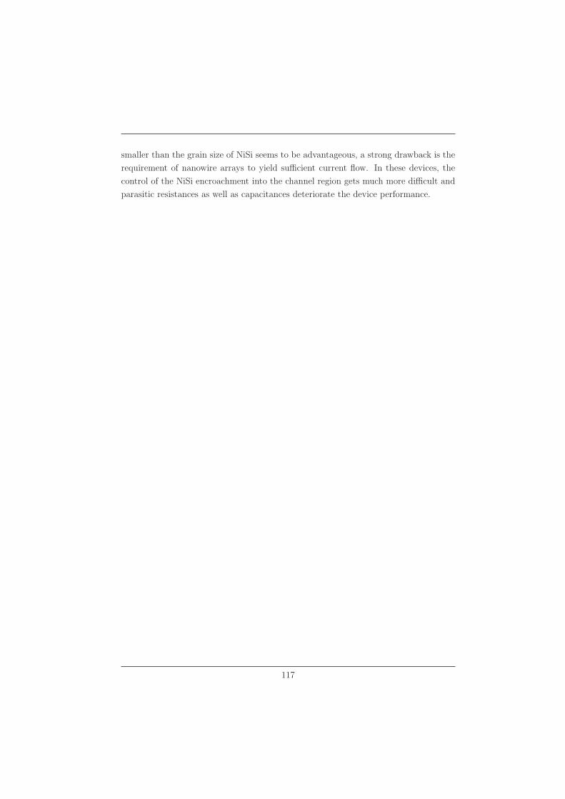
smaller than the grain size of NiSi seems to be advantageous, a strong drawback is the
requirement of nanowire arrays to yield sufficient current flow. In these devices, the
control of the NiSi encroachment into the channel region gets much more difficult and
parasitic resistances as well as capacitances deteriorate the device performance.
117
Chapter 8. Variability
118
Chapter 9
Conclusion and Outlook
Continuous downscaling of today’s MOSFETs requires new innovative device concepts.
In the present thesis, NiSi SB-MOSFETs with silicidation induced dopant segregation
are investigated in detail using DC and RF measurements. This provides physical in-
sights into the operation principle of these devices and more precisely into the carrier
injection. The fabricated devices offer high potential for a use in ultimately scaled
microelectronics.
The physical modeling of NiSi/p-Si Schottky contacts using the proposed numerical
model which combines the thermionic emission theory with image-force induced barrier
lowering and quantum-mechanical tunneling shows a perfect agreement between the
calculated and measured data. A quantitative analysis of the enhanced carrier injec-
tion of Schottky diodes with dopant segregation using B, As or Sb reveals effective
Schottky barrier heights in the 0.1 eV regime below which SB-MOSFETs are able of
outperforming conventional MOSFETs. The corresponding dopant depth profiles mea-
sured by secondary ion mass spectrometry reveal the expected dose-dependent pile-up
of dopants at the NiSi/Si interface which reflects the implantation dose dependence of
the effective Schottky barrier height.
The steadily optimized reproducible process technology for SB-MOSFETs allows the
fabrication of long- and short-channel SB-MOSFETs down to gate-lengths of 80 nm.
The ground-signal-ground layout of the two-finger devices in combination with dedi-
cated test structures is optimized for S-parameter measurements.
DC characterization of the successfully fabricated devices shows drastically improved
electrical performance of SB-MOSFETs with dopant segregation when compared to
SB-MOSFETs without ion implantation. Studies of the dopant dependence of the
device performance indicate that the correct choice of the implantation dose in combi-
nation with the spacer thickness, i. e., the segregation length, is mandatory to achieve
119
Chapter 9. Conclusion and Outlook
superior electrical characteristics. In general, devices with higher implantation doses
exhibit a distinct suppression of the ambipolar behavior and higher on-currents. The
latter are result of a strong reduction of the S/D resistances for devices with high As
dose which is confirmed by the extracted Rs/d values from DC measurements.
80 nm-short channel SB-MOSFETs reveal on-currents as high as 427μA/μm for p-type
and 1150μA/μm for n-type devices, respectively, which compete well with state-of-
the-art SB-MOSFETs fabricated by TSMC, Toshiba and IEMN and highlights their
outstanding performance. SB-MOSFETs fabricated on biaxially strained SOI show si-
milar DC performance for p-type devices when compared with SOI devices. However,
in case of n-type SB-MOSFETs, where a performance increase is expected due to a
higher effective electron mobility, degraded performance is observed which could be a
result of less segregation of As dopants or a contact problem due to abnormal oxidation
of NiSi in the presence of strained silicon.
S-parameter measurements are performed for the first time on short-channel n- and
p-type NiSi SB-MOSFETs with dopant segregation and facilitate the extraction of the
extrinsic and intrinsic device parameters from small-signal parameters. The RF in-
vestigation of SB-MOSFETs fabricated on 20 nm thick SOI reveals a perfectly linear
scaling and high cut-off frequencies fT of 117 GHz for n-type and 63 GHz for p-type
SB-MOSFETs with a gate length of 80 nm. A study of the implantation dose depen-
dence, i. e., different Schottky barrier heights, is carried out on n-type SB-MOSFETs
with an optimized fabrication process. By this, the S/D resistance is improved by 30%
to 508 Ωμm and cut-off frequencies as high as 140 GHz are obtained. The RF study of
these devices with different implantation dose reveals a strongly improved on-current
by a factor of two between the lowest and the highest implantation dose, due to a
drastically reduced S/D resistance, while the cut-off frequency increases only by 20%.
This smaller impact of the Schottky barrier height on the cut-off frequency which is
proportional to Gme/Cgge can be explained by a similar behavior of the transconduc-
tance Gme and total gate capacitance Cgge for different Schottky barrier heights. A
comparison of the cut-off frequencies of the present SB-MOSFETs with state-of-the-art
MOSFETs shows the superior RF performance which is comparable to various devices
with the same gate lengths and indicates an impressive performance increase for fur-
ther downscaling. RF performance limiting parameters are identified and besides the
extrinsic series resistances and overlap capacitances, short-channel effects are found to
be crucial.
The RF variability of the SB-MOSFETs can be related to the depletion capacitance
whose major contributions are the overlap capacitance which is strongly affected by
the NiSi/Si interface roughness and the fringing capacitance.
120
The high potential of NiSi S/D SB-MOSFETs which is demonstrated in this work
can be even improved by combination of dopant segregation with elevated source and
drain. Moreover, the use of high-k gate dielectrics and thinner SOI would result in an
improved electrostatic control. Furthermore, the NiSi/Si interface roughness should be
reduced by using Ni(Pt)Si with smaller grain sizes or ultrathin epitaxial NiSi2 which
simplifies further downscaling of these devices. The integration of dopant segregation
in innovative device concepts like nanowires or FinFETs which provide better electro-
statics than planar devices emerge as promising device structures to minimize crucial
short-channel effects. However, critical device parameters like parasitic resistances and
capacitances which are arising for the new architectures will become a future challenge.
121
Chapter 9. Conclusion and Outlook
122
Bibliography
[1] G. E. Moore. Cramming more components onto integrated circuits. Electronics,
38, 1965.
[2] International Technology Roadmap for Semiconductors, 2008, Update, 2008.
URL http://www.itrs.net.
[3] S Thompson and S Parthasarathy. Moore’s law: the future of Si microelectronics.
Materials Today, 9(6):20–25, 2006.
[4] J. Kedzierski, P. Xuan, E.H. Anderson, and J. Bokor. Complementary silicide
source/drain thin-body MOSFETs for the 20 nm gate length regime. In Inter-
national Electron Devices Meeting 2000. Technical Digest. IEDM, pages 57–60.
IEEE, 2000. ISBN 0-7803-6438-4.
[5] Y. Nishi. Insulated gate field effect transistor and it manufacturing method, 1970.
[6] M. P. Lepselter and S. M. Sze. SB-IGFET: An insulated-gate filed-effect transis-
tor using Shottky barrier contacts for the source and drain. Proc., IEEE, 56(8):
1400–1402, 1968.
[7] D. Connelly, C. Faulkner, and D. E. Grupp. Optimizing schottky S/D offset
for 25-nm dual-gate cmos performance. IEEE Electron Device Letters, 24(6):
411–413, 2003.
[8] S. Xiong, T.-J. King, and J. Bokor. A comparison study of symmetric ultrathin-
body double-gate devices with metal source/drain and doped source/drain. IEEE
Transactions on Electron Devices, 52(8):1859–1867, 2005.
[9] X. Tang. Very low Schottky barrier to n-type silicon with PtEr-stack silicide.
Solid-State Electronics, 47(11):2105–2111, 2003.
[10] M. Jang, Y. Kim, J. Shin, and K. Park. A 50-nm-gate-length erbium-silicided n-
type Schottky barrier metal-oxide-semiconductor field-effect transistor. Applied
Physics Letters, 84(5):741–743, 2004.
123
Bibliography
[11] S. Zhu, C. X. Zhu, J. Chen, M. F. Li, S. J. Lee, J. Singh, A. Du, C. H. Tung,
A. Chin, and D. L. Kwong. N-type Schottky barrier source/drain MOSFET using
ytterbium silicide. IEEE Electron Device Letters, 25(8):565–567, 2004.
[12] J. M. Larson and J. P. Snyder. Overview and status of metal S/D Schottky-
barrier MOSFET technology. IEEE Transactions on Electron Devices, 53(5):
1048–1058, 2006.
[13] M. Fritze, C. L. Chen, S. Calawa, D. Yost, B. Wheeler, P. Wyatt, C. L. Keast,
J. Snyder, and J. Larson. High-speed Schottky-barrier pMOSFET with fT = 280
GHz. IEEE Electron Device Letters, 25(4):220–222, 2004.
[14] D. Connelly, C. Faulkner, P. A. Clifton, and D. Grupp. Fermi-level depinning
for low-barrier Schottky source/drain transistors. Applied Physics Letters, 88(1):
012105, 2006.
[15] H. Ghoneim, J. Knoch, H. Riel, D. Webb, M. T. Bjork, and S. Karg. Inter-
face engineering for the suppression of ambipolar behavior in Schottky barrier
MOSFETs. In Ultimate Integration of Silicon, ULIS 2009. 10th International
Conference on., pages 69–72, 2009.
[16] H. Ghoneim, M. T. Bjork, J. Knoch, E. Lortscher, H. Riel, D. Webb, S. Karg,
H. Schmid, and W. Riess. Suppression of ambipolar behavior in metallic
source/drain metal-oxide-semiconductor field-effect transistors. Applied Physics
Letters, 95(21):213504, 2009.
[17] G. Larrieu, E. Dubois, R. Valentin, N. Breil, F. Danneville, G. Dambrine, J.-P.
Raskin, and J.C. Pesant. Low temperature implementation of dopant-segregated
band-edge metallic S/D junctions in thin-body SOI p-MOSFETs. In 2007 IEEE
International Electron Devices Meeting, number 1, pages 147–150. IEEE, 2007.
[18] Z. Zhang, J. Lu, Z. Qiu, P. E. Hellstrom, and M. Ostling. Performance fluctuation
of FinFETs with Schottky barrier source/drain. IEEE Electron Device Letters,
29(5):506–508, 2008.
[19] S.-L. Zhang, M. Zhang, J. Knoch, S. Feste, M. Schroter, and S. Mantl. Threshold
voltage variation in SOI Schottky-barrier MOSFETs. IEEE Transactions on
Electron Devices, 55(3):858–865, 2008.
[20] T. Yamauchi, A. Kinoshita, Y. Tsuchiya, J. Koga, and K. Kato. 1 nm NiSi/Si
junction design based on first-principles calculation for ultimately low contact
resistance. In IEEE Electron Devices Meeting, 2006. IEDM’06. International,
pages 1–4, 2006.
124
Bibliography
[21] T. Yamauchi, Y. Nishi, Y. Tsuchiya, A. Kinoshita, J. Koga, and K. Kato. Novel
doping technology for a 1nm NiSi/Si junction with dipoles comforting Schottky
(DCS) barrier. In IEEE International Electron Devices Meeting, 2007. IEDM
2007, pages 963–966, 2007.
[22] T. Marukame, T. Yamauchi, Y. Nishi, T. Sasaki, A. Kinoshita, J. Koga, and
K. Kato. Impact of platinum incorporation on thermal stability and interface
resistance in NiSi/Si junctions based on first-principles calculation. In IEEE
Electron Devices Meeting, 2008. IEDM’08. International, pages 547–550, 2008.
[23] Y. Taur and T. H. Ning. Fundamentals of modern VLSI devices. Cambridge
University Press, Cambridge, 1 edition, 2000.
[24] S. M. Sze. Physics of semiconductor devices. John Wiley & Sons, Hoboken, third
edition, 2007.
[25] J.-P. Colinge and C. A. Colinge. Physics of semiconductor devices. Kluwer
Academic Publishers, New York, first edition, 2002.
[26] S. Datta. Quantum Transport - Atom to Transistor. Cambridge University Press,
Cambridge, third edition, 2007.
[27] H. C. Pao and C. T. Sah. Effects of diffusion current in characteristics of metal-
oxide (insulator)-semiconductor transistors. Solid-State Electronics, 9:927–937,
1966.
[28] J. R. Brews. A charge-sheet model of the MOSFET. Solid-State Electronics, 21:
345–355, 1978.
[29] A. Rahman, J. Guo, S. Datta, and M. S. Lundstrom. Theory of ballistic nan-
otransistors. IEEE Transactions on Electron Devices, 50(9):1853–1864, 2003.
[30] M. Lundstrom. Notes on the ballistic MOSFET, 2005.
[31] A. Ortiz-Conde, F. J. Garcıa Sanchez, J. J. Liou, A. Cerdeira, M Estrada, and
Y. Yue. A review of recent MOSFET threshold voltage extraction methods.
Microelectronics Reliability, 42:583–596, 2002.
[32] K. Terada, K. Nishiyama, and K.-I. Hatanaka. Comparison of MOSFET-
threshold-voltage extraction methods. Solid-State Electronics, 45:35–40, 2001.
[33] M. Tsuno, M. Suga, M. Tanaka, K. Shibahara, M. Miura-Mattausch, and M. Hi-
rose. Physically-based threshold voltage determination for MOSFET’s of all gate
lengths. IEEE Transactions on Electron Devices, 46(7):1429–1434, 1999.
125
Bibliography
[34] H.-S. Wong, M. H. White, T. J. Krutsick, and R. V. Booth. Modeling of transcon-
ductance degradation and extraction of threshold voltage in thin oxide MOS-
FET’s. Solid-State Electronics, 30(9):953–968, 1987.
[35] J. Appenzeller, Y.-M. Lin, J. Knoch, and Ph. Avouris. Band-to-band tunneling
in carbon nanotube field-effect transistors. Physical Review Letters, 93(19):1–4,
2004.
[36] C. Aydin, A. Zaslavsky, S. Luryi, S. Cristoloveanu, D. Mariolle, D. Fraboulet,
and S. Deleonibus. Lateral interband tunneling transistor in silicon-on-insulator.
Applied Physics Letters, 84(10):1780, 2004.
[37] K. Boucart and A. M. Ionescu. Double-gate tunnel FET with high-κ gate dielec-
tric. IEEE Transactions on electron devices, 54(7):1725–1733, 2007.
[38] F. Mayer, C. Le Royer, J.-F. Damlencourt, K. Romanjek, F. Andrieu, and
C. Tabone. Impact of SOI, Si1−xGexOI and GeOI substrates on CMOS com-
patible tunnel FET performance. Tech. Dig., pages 163–167, 2008.
[39] C. Sandow, J. Knoch, C. Urban, Q.-T. Zhao, and S. Mantl. Impact of electro-
statics and doping concentration on the performance of silicon tunnel field-effect
transistors. Solid-State Electronics, 53:1126–1129, 2009.
[40] H. S. Momose, E. Morifuji, T. Yoshitomi, T. Ohguro, M. Saito, and H. Iwai.
Cutoff frequency and propagation delay time of 1.5-nm gate oxide CMOS. IEEE
Transactions on Electron Devices, 48(6):1165–1174, 2001.
[41] Y.-K. Choi, D. Ha, T.-J. King, and J. Bokor. Investigation of gate-induced
drain leakage (GIDL) current in thin body devices: single-gate ultra-thin body,
symmetrical double-gate, and asymmetrical double-gate MOSFETs. Japanese
Journal of Applied Physics, 42(Part 1, No. 4B):2073–2076, 2003.
[42] J.-P. Colinge. Silicon-on-insulator technology: materials to VLSI. Kluwer Aca-
demic Publishers, Boston, third edition, 2004.
[43] J. Koomen. Investigation of the MOST channel conductance in weak inversion.
16(7):801–810, 1973.
[44] C. Sodini, T. Ekstedt, and J. Moll. Charge accumulation and mobility in thin
dielectric MOS transistors. Solid-State Electronics, 25(9):833–841, 1982.
[45] G Baccarani, M. R. Wordeman, and R. H. Dennard. Generalized scaling the-
ory and its application to a 1/4 micrometer MOSFET. IEEE Transactions on
Electron Devices, 31:452, 1984.
126
Bibliography
[46] R.-H. Yan, A. Ourmazd, and K. F. Lee. Scaling the Si MOSFET: from bulk to
SOI to bulk. IEEE Transactions on Electron Devices, 39(7):1704–1710, 1992.
[47] R. H. Dennard, F. H. Gaensslen, H.-N. Yu, V. L. Rideout, E. Bassous, and A. R.
LeBlanc. Design of ion-implanted MOSFET’s with very small physial dimensions.
IEEE Journal of Solid State Circuits, 9:256, 1974.
[48] M. Depas, B. Vermeire, P. W. Mertens, R. L. Van Meirhaeghe, and M. M. Heyns.
Determination of tunneling parameters in ultra-thin oxide layer poly-Si/SiO2/Si
structures. Solid-State Electronics, 38(8):1465–1471, 1995.
[49] J. R. Brews, W. Fichtner, E. H. Nicollian, and S. M. Sze. Generalized guide for
MOSFET miniaturization. IEEE Electron Device Letters, 1:2, 1980.
[50] J.-P. Colinge. The new generation of SOI MOSFETs. Romanian Journal of
Information Science and Technology, 11(1):3–15, 2008.
[51] T. Tsuchiya, Y. Sato, and M. Tomizawa. Three mechanisms determining short-
channel effects in fully-depleted SOI MOSFETs. IEEE Transactions on Electron
Devices, 45(5):1116–1121, 1998.
[52] S. Veeraraghavan and J. Fossum. Short-channel effects in SOI MOSFET’s. IEEE
Transactions on Electron Devices, 36:522–528, 1989.
[53] S.-L. Zhang and M. Ostling. Metal silicides in CMOS technology: past, present
and future trends. Critical Reviews in Solid State and Material Sciences, 28(1):
1–129, 2003.
[54] H. Iwai, T. Ohgura, and S.-I. Ohmi. NiSi salicide technology for scaled CMOS.
Microelectronic Engineering, 60(1-2):157–169, 2002.
[55] R.L. Thornton. Schottky-barrier elevation by ion implantation and implant seg-
regation. Electronics Letters, 17(14):485–486, 1981.
[56] M. Wittmer and K. N. Tu. Low-temperature diffusion of dopant atoms in silicon
during interfacial silicide formation. Physical Review B, 29(4):2010, 1984.
[57] Z. Qiu, Z. Zhang, M. Ostling, and S.-L. Zhang. A comparative study of two
different schemes to dopant segregation at NiSi/Si and PtSi/Si interfaces for
Schottky barrier height lowering. IEEE Transactions on Electron Devices, 55(1):
396–403, 2008.
[58] E. Dubois. Schottky barrier MOSFETs. unpublished, 2009.
127
Bibliography
[59] E. H. Rhoderick and R. H. Williams. Metal-semiconductor contacts. Clarendon
Press, Oxford, 1988.
[60] A. Ferhat-Hamida, Z. Ouennoughi, A. Hoffmann, and R. Weiss. Extraction
of Schottky diode parameters including parallel conductance using a vertical
optimization method. Solid-State Electronics, 46(5):615–619, 2002.
[61] E. K. Evangelou, L. Papadimitriou, C. A. Dimitriades, and G. E. Giakoumakis.
Extraction of Schottky diode (and pn junction) parameters from IV characteris-
tics. Solid-State Electronics, 36(11):1633–1633, 1993.
[62] Z. Zhang, Z. Qiu, M. Ostling, and S.-L. Zhang. Schottky-barrier height tuning
by means of ion implantation into preformed silicide films followed by drive-in
anneal. IEEE Electron Device Letters, 28(7):565–568, 2007.
[63] H. Norde. A modified forward I-V plot for Schottky diodes with high series
resistance. Journal of Applied Physics, 50:5052, 1979.
[64] A. Saxena. Forward current-voltage characteristics of Schottky barriers on n-type
silicon. Surface Science, 13:151–171, 1969.
[65] V. Mikhelashvili, G. Eisenstein, and R. Uzdin. Extraction of Schottky diode
parameters with a bias dependent barrier height. Solid State Electronics, 45(1):
143–148, 2001.
[66] J. R. Jimenez, X. Xiao, J. C. Sturm, and P. W. Pellegrini. Tunable, long-
wavelength PtSi/SiGe/Si Schottky diode infrared detectors. Applied Physics
Letters, 67(4):506, 1995.
[67] E. Dubois and G. Larrieu. Measurement of low Schottky barrier heights applied to
metallic source/drain metal-oxide-semiconductor field effect transistors. Journal
of Applied Physics, 96(1):729, 2004.
[68] M. Muller. Schottky-barrier height tuning using dopant segregation for NiGe/Ge
and PtGe2/Ge contacts. Diploma thesis, 2008.
[69] C. R. Crowell and V. L. Rideout. Normalized thermionic-field (TF) emission in
metal-semiconductor (Schottky) barriers. Solid-State Electronics, 12(2):89–105,
1969.
[70] K. Maex and M. Van Rossum, editors. Metal silicides. Inspec, 1995.
[71] M. Zhang. Modelling and fabrication of high performance Schottky-barrier SOI-
MOSFETs with low effective Schottky barriers. PhD thesis, 2006.
128
Bibliography
[72] C. Urban, Q.-T. Zhao, C. Sandow, M. Muller, U. Breuer, and S. Mantl. Schottky
barrier height modulation by arsenic dopant segregation. 2008 9th International
Conference on Ultimate Integration of Silicon, (100):151–154, 2008.
[73] Q. T. Zhao, U. Breuer, E. Rije, and S. Mantl. Tuning of NiSi/ Si Schottky barrier
heights by sulfur segregation during Ni silicidation. Applied Physics Letters, 86:
062108, 2005.
[74] E. Alptekin, M. C. Ozturk, and V. Misra. Tuning of the platinum silicide Schottky
barrier height on n-type silicon by sulfur segregation. IEEE Electron Device
Letters, 30(4):331–333, 2009.
[75] S. A. Wartenberg. RF measurements of die and packages. Artech House, Nor-
wood, first edition, 2002.
[76] W. Kern. The evolution of silicon wafer cleaning technology. Journal of The
Electrochemical Society, 137(6):1887, 1990.
[77] M. C. Lemme, T. Mollenhauer, H. Gottlob, W. Henschel, J. Efavi, C. Welch,
and H. Kurz. Highly selective HBr etch process for fabrication of triple-gate
nano-scale SOI-MOSFETs. Microelectronic Engineering, 73:346–350, 2004.
[78] H. Nicollian and J. R. Brews. MOS technology. Wiley, New York, 1982.
[79] E. Durgun Ozben. The effects of prior nitridation process of silicon surface and
different metal gates on the capacitance voltage characteristics of metal-Ta2O5-Si
MOS capacitor, 2007.
[80] K. Maex and M. Van Rossum. Properties of metal silicides. Institution of Elec-
trical Engineers, London, 1995.
[81] C. Wang, J. P Snyder, and J. R. Tucker. Sub-40 nm PtSi Schottky source/drain
metal-oxide-semiconductor field-effect transistors. Applied Physics Letters, 74(8):
1174–1176, 1999.
[82] R. Valentin, E. Dubois, J.-P. Raskin, G. Larrieu, G. Dambrine, T. C. Lim,
N. Breil, and F. Danneville. RF small-signal analysis of Schottky-barrier p-
MOSFET. IEEE Transactions on Electron Devices, 55(5):1192–1202, 2008.
[83] J. Knoch, M. Zhang, S. Feste, and S. Mantl. Dopant segregation in SOI Schottky-
barrier MOSFETs. Microelectronic Engineering, 84(11):2563–2571, 2007.
[84] D. Lenoble. Advanced junction fabrication challenges at the 45nm node. Semi-
conductor Fabtech (www.fabtech.org), 2006.
129
Bibliography
[85] T. Skotnicki. Materials and device structures for sub-32 nm CMOS nodes. Mi-
croelectronic Engineering, 84(9-10):1845–1852, 2007.
[86] K. Terada and H. Muta. A new method to determine effective MOSFET channel
length. Jap. J. Appl. Phys, 18(5):953, 1979.
[87] D.K. Schroder. Semiconductor material device characterization. John Wiley &
Sons, New York, 1998.
[88] S.E. Thompson, G. Sun, Y.S. Choi, and T. Nishida. Uniaxial-process-induced
strained-Si: extending the CMOS roadmap. IEEE Transactions on electron De-
vices, 53(5):1010–1020, 2006.
[89] M. Horstmann, M. Wiatr, A. Wei, J. Hoentschel, Th. Feudel, Th. Scheiper,
R. Stephan, M. Gerhadt, S. Krugel, and M. Raab. Advanced SOI CMOS tran-
sistor technology for high performance microprocessors. Solid-State Electronics,
53(12):1212–1219, 2009.
[90] D. Buca, B. Hollander, H. Trinkaus, S. Mantl, R. Carius, R. Loo, M. Caymax,
and H. Schaefer. Tensely strained silicon on SiGe produced by strain transfer.
Applied Physics Letters, 85(13):2499, 2004.
[91] B. Ghyselen, J.-M. Hartmann, T. Ernst, C. Aulnette, B. Osternaud, Y. Bogu-
milowicz, A. Abbadie, P. Besson, O. Rayssac, A. Tiberj, N. Daval, I. Cayrefourq,
F. Fournel, H. Moriceau, C. Di Nardo, F. Andrieu, V. Paillard, M. Cabie, L. Vin-
cent, E. Snoeck, F. Cristiano, A. Rocher, A. Ponchet, A. Claverie, P. Boucaud,
M.-N. Semeria, D. Bensahel, N. Kernevez, and C. Mazure. Engineering strained
silicon on insulator wafers with the smart Cut technology. Solid-State Electronics,
48(8):1285–1296, 2004.
[92] M. L. Lee, E. A. Fitzgerald, M. T. Bulsara, M. T. Currie, and A. Lochtefeld.
Strained Si, SiGe, and Ge channels for high-mobility metal-oxide-semiconductor
field-effect transistors. Journal of Applied Physics, 97(1):011101, 2005.
[93] S. Takagi, T. Mizuno, T. Tezuka, N. Sugiyama, S. Nakaharai, T. Numata,
J. Koga, and K. Uchida. Sub-band structure engineering for advanced CMOS
channels. Solid-State Electronics, 49(5):684–694, 2005.
[94] S. F. Feste, Th. Schapers, D. Buca, Q. T. Zhao, J. Knoch, M. Bouhassoune,
A. Schindlmayr, and S. Mantl. Measurement of effective electron mass in biaxial
tensile strained silicon on insulator. Applied Physics Letters, 95(18):182101, 2009.
130
Bibliography
[95] J.-G. Yun, S.-Y. Oh, H.-H. Ji, B.-F. Huang, Y.-H. Park, J.-S. Wang, S.-H. Park,
T.-S. Bae, and H.-D. Lee. Abnormal oxidation of nickel silicide on n-type sub-
strate and effect of preamorphization implantation. Japanese Journal of Applied
Physics, 43(10):6998–6999, 2004.
[96] C. H. Ko, H. W. Chen, T. J. Wang, T. M. Kuan, J. W. Hsu, C. Y. Huang,
C. H. Ge, L. S. Lai, and W. C. Lee. NiSi Schottky barrier process-strained Si
(SB-PSS) CMOS technology for high performance applications. In Symposium
on VLSI Technology Digest of Technical Papers 2006, number c, pages 80–81,
2006.
[97] T. Kinoshita, R. Hasumi, M. Hamaguchi, K. Miyashita, T. Komoda, A. Ki-
noshita, J. Koga, K. Adachi, Y. Toyoshima, T. Nakayama, S. Yamada, and
F. Matsuoka. Ultra low voltage operations in bulk CMOS logic circuits with
dopant segregated Schottky source/drain transistors. IEEE Electron Devices
Meeting, 2006. IEDM’06. International, 2006.
[98] L. Hutin, M. Vinet, T. Poiroux, C. Le Royer, B. Previtali, C. Vizioz, D. Lafond,
Y. Morand, M. Rivoire, F. Nemouchi, V. Carron, T. Billon, S. Deleonibus, and
O. Faynot. Dual metallic source and drain integration on planar single and double
gate SOI CMOS down to 20nm: performance and scalability assessment. IEEE
International Electron Devices Meeting, 2009. IEDM Technical Digest, pages 45–
48, 2009.
[99] Agilent-Technologies. Agilent AN 154 - S-parameter design. Application Note.
[100] U. Tietze and Ch. Schenk. Halbleiter-Schaltungstechnik. Springer Verlag, Berlin
Heidelberg, 12. edition, 2002.
[101] J.-P. Raskin. Modeling, characterization and optimization of MOSFET’s and
passive elements for the synthesis of SOI MMIC’s, 1997.
[102] J.-P. Raskin, R. Gillon, D. Vanhoenacker-Janvier, and J.-P. Colinge. Accurate
SOI MOSFET characterization at microwave frequencies for device performance
optimization and analog modeling. IEEE Transactions on Electron Devices, 45
(5):1017–1025, 1998.
[103] Y. Tsividis. Operation and modeling of the MOS transistor. Oxford University
Press, Oxford, second edition, 2003.
[104] A. Bracale, J. L. Gautier, V. Ferlet-Cavrois, N. Fel, D. Pasquet, J L. Pelloie,
and J. Du Port De Poncharra. A new approach for SOI devices small-signal
131
Bibliography
parameters extraction. Analog Integrated Circuits and Signal Processing, 25:157–
169, 2000.
[105] H. Cho and D. E. Burk. A three-step method for de-embedding of high-frequency
S-parameter measurements. IEEE Transactions on Electron Devices, 38(6):1371–
1375, 1991.
[106] J. C. Tinoco and J.-P. Raskin. New RF extrinsic resistances extraction proce-
dure for deep-submicron MOS transistors. International Journal of Numerical
modelling: Electronic Networks, Devices and Fields, 2009.
[107] J.-P. Raskin. Private lecture, 2009.
[108] Hewlett-Packard. Specifying calibration standards for the HP 8510 network an-
alyzer. Hewlett-Packard Product Note 8510-5, 1986.
[109] M. Emam, J. Tinoco, D. Vanhoenacker-Janvier, and J.-P. Raskin. High-
temperature DC and RF behaviors of partially-depleted SOI MOSFET tran-
sistors. Solid-State Electronics, 52(12):1924–1932, 2008.
[110] J.-P. Raskin. Personal email, 2009.
[111] P. Zhao, M. Kim, B. Gnade, and R. Wallace. Dopant effects on the thermal
stability of FUSI NiSi. Microelectronic Engineering, 85(1):54–60, 2008.
[112] J. Knoch and J. Appenzeller. Carbon nanotube field-effect transistors - the im-
portance of being small, chapter 6.2, pages 371–402. Springer Netherlands, 2006.
[113] A. Kasamatsu, K. Kasai, K. Hikosaka, T. Matsui, and T. Mimura. 60 nm gate-
length Si/SiGe HEMT. Applied Surface Science, 224:382–385, 2004.
[114] G. Dambrine, C. Raynaud, D. Lederer, M. Dehan, O. Rozeaux, M. Vanmackel-
berg, F. Danneville, S. Lepilliet, and J.-P. Raskin. What are the Limiting Pa-
rameters of Deep-Submicron MOSFETs for High Frequency Applications? IEEE
Electron Device Letters, 24(3):189–191, 2003.
[115] K. Romanjek, F. Andrieu, T. Ernst, and G. Ghibaudo. Characterization of the
effective mobility by split C(V) technique in sub 0.1μm Si and SiGe PMOSFETs.
Solid-State Electronics, 49(5):721–726, 2005.
[116] A. Siligaris, G. Pailloncy, S. Delcourt, R. Valentin, S. Lepilliet, F. Danneville,
D. Gloria, and G. Dambrine. High-frequency and noise performances of 65-
nm MOSFET at liquid nitrogen temperature. IEEE Transactions on Electron
Devices, 53(8):1902–1908, 2006.
132
Bibliography
[117] S. Mason. Cover gain in feedback amplifier. Circuit Theory, Transaction of the
IRE Professional Group on, 1(2):20–25, 1954.
[118] R. Valentin, E. Dubois, G. Larrieu, J.-P. Raskin, G. Dambrine, N. Breil, and
F. Danneville. Optimization of RF performance of metallic source/drain SOI
MOSFETs using dopant segregation at the Schottky interface. IEEE Electron
Device Letters, 30(11):1197–1199, 2009.
[119] J.N. Burghartz, M. Hargrove, C.S. Webster, R.A. Groves, M. Keene, K.A. Jenk-
ins, R. Logan, and E. Nowak. RF potential of a 0.18-μm CMOS logic device
technology. IEEE Trans. Electron Devices, 47(4):864–870, 2000.
[120] D. Barlage, R. Arghavani, G. Dewey, M. Doczy, B. Doyle, J. Kavalieros,
A. Murthy, B. Roberds, P. Stokley, and R. Chau. High-frequency response of
100 nm integrated CMOS transistors with high-K gate dielectrics. Electron De-
vices Meeting, 2001. IEDM Technical Digest. International, pages 10–6, 2001.
[121] T. Matsumoto, S. Maeda, K. Ota, Y. Hirano, K. Eikyu, H. Sayama, T. Iwamatsu,
K. Yamamoto, T. Katoh, and Y. Yamaguchi. 70 nm SOI-CMOS of 135 GHz f
max with dualoffset-implanted source-drain extension structure for RF/analog
andlogic applications. Electron Devices Meeting, 2001. IEDM Technical Digest.
International, pages 10–3, 2001.
[122] T. Hashimoto, Y. Nonaka, T. Saito, K. Sasahara, T. Tominari, K. Sakai, K. Toku-
naga, T. Fujiwara, S. Wada, T. Udo, T. Jinbo, K. Washio, and H. Hosoe. In-
tegration of a 0.13-μm CMOS and a high performance self-aligned SiGe HBT
featuring low base resistance. Digest. International Electron Devices Meeting,,
pages 779–782, 2002.
[123] N. Zamdmer, J. O. Plouchart, J. Kim, L. H. Lu, S. Narasimha, P. A. O’Neil,
A. Ray, M. Sherony, and L. Wagner. Suitability of scaled SOI CMOS for high-
frequency analog circuits. Proceedings of the European Solid-State Device Re-
search Conference, pages 511–514, 2002.
[124] A. Chatterjee, J. Yoon, S. Zhao, S. Tang, K. Sadra, S. Crank, H. Mogul, R. Ag-
garwal, B. Chatterjee, and S. Lytle. A 65 nm CMOS technology for mobile
and digital signal processing applications. IEEE International Electron Devices
Meeting, 2004. IEDM Technical Digest, pages 665–668, 2004.
[125] S. Narasimha, A. Ajmera, H. Park, D. Schepis, N. Zamdmer, K.a. Jenkins, J.-
O. Plouchart, W.-H. Lee, J. Mezzapelle, J. Bruley, B. Doris, J.W. Sleight, S.K.
Fung, S.H. Ku, A.C. Mocuta, I. Yang, P.V. Gilbert, K.P. Muller, P. Agnello,
133
Bibliography
and J. Welser. High performance sub-40 nm CMOS devices on SOI for the 70
nm technology node. International Electron Devices Meeting. Technical Digest,
pages 29.2.1–29.2.4, 2001.
[126] Y. Mii, S. Rishton, Y. Taur, D. Kern, T. Lii, K. Lee, K.A. Jenkins, D. Quinlan,
T. Brown, D. Danner, F. Sewell, and M. Polcari. Experimental high performance
sub-0.1 μm channel nMOSFET’s. IEEE Electron Device Letters, 15(1):28–30,
1994.
[127] M. Saito, M. Ono, R. Fujimoto, H. Tanimoto, N. Ito, T. Yoshitomi, T. Ohguro,
H. S. Momose, and H. Iwai. 0.15-μm RF CMOS technology compatible with
logic CMOS for low-voltage operation. IEEE Transactions on Electron Devices,
45(3):737–742, 1998.
[128] C. Wann, F. Assaderaghi, L. Shi, K. Chan, S. Cohen, H. Hovel, K. Jenkins,
Y. Lee, D. Sadana, R. Viswanathan, S. Wind, and Y. Taur. High-performance
0.07-μm CMOS with 9.5-ps gate delay and 150GHz ft. IEEE Electron Device
Letters, 18(12):625–627, 1997.
[129] Y. Taur, S. Wind, Y. J. Mii, Y. Lii, D. Moy, K. A. Jenkins, C. L. Chen, P. J.
Coane, D. Klaus, and J. Bucchignano. High performance 0.1 μm CMOS devices
with 1.5 V power supply. Electron Devices Meeting, 1993. IEDM’93. Technical
Digest., International, pages 127–130, 1993.
[130] T. Ohguro, H. Naruse, H. Sugaya, E. Morifuji, S. Nakamura, T. Yoshitomi,
T. Morimoto, HS Momose, Y. Katsumata, and H. Iwai. 0.18 μm low voltage/low
power RF CMOS with zero Vth analog MOSFETs made by undoped epitaxial
channel technique. Electron Devices Meeting, 1997. IEDM’97. Technical Digest.,
International, pages 837–840, 1997.
[131] T. Ohguro, H. Naruse, H. Sugaya, H. Kimijima, E. Morifuji, T. Yoshitomi,
T. Morimoto, H. S. Momose, Y. Katsumata, and H. Iwai. 0.12 μm raised
gate/source/drain epitaxial channel NMOS technology. International Electron
Devices Meeting 1998. Technical Digest, pages 927–930, 1998.
[132] K. F. Lee, R. H. Yan, D. Y. Jeon, D. M. Tennant, E. H. Westerwick, G. M. Chin,
M. D. Morris, R. W. Johnson, T. M. Liu, R. C. Kistler, A. M. Voshchenkov,
R. G. Swartz, and A. Ourmazd. 0.1 μm p-channel MOSFET with 51GHz fT .
International Electron Devices Meeting 1992. Technical Digest, pages 1012–14,
1992.
134
Bibliography
[133] D. J. Pearman, G. Pailloncy, J.-P. Raskin, J. M. Larson, J. P. Snyder, E. H. C.
Parker, and T. E. Whall. Static and high-frequency behavior and performance of
Schottky-barrier p-MOSFET devices. IEEE Transactions on Electron Devices,
54(10):2796–2802, 2007.
[134] J.-P. Raskin, D. J. Pearman, G. Pailloncy, J. M. Larson, J. Snyder, D. L. Leadley,
and T. E. Whall. High-frequency performance of Schottky source/drain silicon
pMOS devices. IEEE Electron Device Letters, 29(4):396–398, 2008.
[135] S. Lee, B. Jagannathan, S. Narasimha, A. Chou, N. Zamdmer, J. Johnson,
R. Williams, L. Wagner, J. Kim, J.-O. Plouchart, J. Pekarik, S. Springer, and
G. Freeman. Record RF performance of 45-nm SOI CMOS technology. 2007
IEEE International Electron Devices Meeting, pages 255–258, 2007.
[136] I. Post, M. Akbar, G. Curello, S. Gannavaram, W. Hafez, U. Jalan, K. Komeyli,
J. Lin, N. Lindert, J. Park, J. Rizk, G. Sacks, C. Tsai, D. Yeh, P. Bai, and C.-H.
Jan. A 65nm CMOS SOC technology featuring strained silicon transistors for
RF applications. In 2006 International Electron Devices Meeting, volume 224,
pages 1–3. IEEE, 2006. ISBN 1-4244-0438-X.
[137] J. Knoch, M. Zhang, S. Manti, and J. Appenzeller. On the performance of single-
gated ultrathin-body SOI Schottky-barrier MOSFETs. IEEE Transactions on
Electron Devices, 53(7):1669, 2006.
[138] J.-P. Raskin, V. Kilchytska, D. Lederer, and D. Flandre. Analog/RF performance
of multiple gate SOI devices: wideband simulations and characterization. IEEE
Transactions on Electron Devices, 53(5):1088–1095, 2006.
[139] S. Nuttinck, B. Parvais, Gi. Curatola, and A. Mercha. Double-gate FinFETs as
a CMOS technology downscaling option: an RF perspective. IEEE Transactions
on Electron Devices, 54(2):279–283, 2007.
[140] J.-P. Raskin. SOI technology: an opportunity for RF designers? In EU-
ROSOI2009 - Fifth Workshop of the Thematic Network on Silicon-On-Insulator
- Turorial: From Modelling to Design, Goteborg, 2009.
[141] J. Kittl, K. Opsomer, C. Torregiani, C. Demeurisse, S. Mertens, D. Brunco,
M. Vandal, and A. Lauwers. Silicides and germanides for nano-CMOS applica-
tions. Materials Science and Engineering: B, 154-155:144–154, 2008.
[142] K. Ohuchi, C. Lavoie, C. Murray, C. D’Emic, I. Lauer, J. O. Chu, B. Yang,
P. Besser, L. Gignac, J. Bruley, G. Singco, F. Pagette, A. W. Topol, M. J. Rooks,
135
Bibliography
J. J. Bucchignano, V. Narayanan, M. Khare, M. Takayanagi, K. Ishimaru, D.-G.
Park, G. Shahidi, and P. Solomon. Extendibility of NiPt silicide contacts for
CMOS technology demonstrated to the 22-nm node. 2007 IEEE International
Electron Devices Meeting, pages 1029–1031, 2007.
[143] L. Knoll, Q. T. Zhao, S. Habicht, C. Urban, B. Ghyselen, and S. Mantl. Ultra
thin Ni-silicides with low cantact resistance on strained and unstrained silicon.
submitted to IEEE Electron Device Letters, 2009.
136

Appendix
137

Appendix A
Abbreviations
BOX buried oxide
CHF3 trifluoromethane
CET capacitance equivalent thickness
CMOS complementary metal oxide semiconductor
CPW coplanar waveguide
C-V capacitance-voltage
DC direct-current
DIBL drain induced barrier lowering
DS dopant segregation
DUT device under test
e-beam electron-beam
eSBH effective Schottky barrier height
ErSi erbium-silicide
FET field-effect transistor
GSG ground-signal-ground
FIB focused ion-beam
H2O2 hydrogen peroxide
H2SO4 sulfuric acid
HBr hydrogen bromide
HF hydroflouric acid
HSQ hydrogen silesquioxane
ICP inductively coupled plasma
ITRS International Technology Roadmap for Semiconductors
I-V current-voltage
139
Appendix A. Abbreviations
LPCVD low pressure chemical vapor deposition
LRRM line-reflect-reflect-match
MIGS metal-induced gap states
MOS metal-oxide-semiconductor
MOSFET metal-oxide-semiconductor field-effect transistor
NiSi nickel silicide
PAM pre-allocation markers
PtSi platinum silicide
RF radio frequency
RIE reactive ion etching
RMS root mean square
RTP rapid thermal processing
Salicide self-aligned silicide
SB Schottky barrier
SBH Schottky barrier height
SCE short-channel effects
SEM scanning electron microscopy
SF6 sulfur hexafluoride
SIMS secondary ion mass spectrometry
S/D source/drain
SOI silicon on insulator
S-parameter scattering parameter
SPM sulfuric acid-hydrogen peroxide mixture
sSOI strained silicon on insulator
STEM scanning transmission electron microscopy
TEM transmission electon microscopy
TEOS tetra-ethyl-ortho-silicate
UTB ultra-thin body
ULG unilateral power gain
VNA vector network analyzer
XRR X-ray refectivity
YbSi ytterbium silicide
140
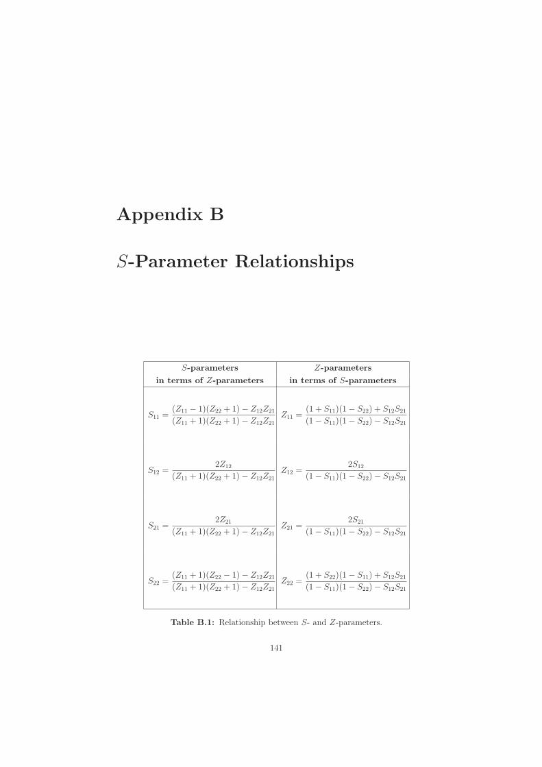
Appendix B
S-Parameter Relationships
S-parameters Z-parameters
in terms of Z-parameters in terms of S-parameters
S11 =(Z11 − 1)(Z22 + 1) − Z12Z21
(Z11 + 1)(Z22 + 1) − Z12Z21
Z11 =(1 + S11)(1 − S22) + S12S21
(1 − S11)(1 − S22) − S12S21
S12 =2Z12
(Z11 + 1)(Z22 + 1) − Z12Z21
Z12 =2S12
(1 − S11)(1 − S22) − S12S21
S21 =2Z21
(Z11 + 1)(Z22 + 1) − Z12Z21
Z21 =2S21
(1 − S11)(1 − S22) − S12S21
S22 =(Z11 + 1)(Z22 − 1) − Z12Z21
(Z11 + 1)(Z22 + 1) − Z12Z21
Z22 =(1 + S22)(1 − S11) + S12S21
(1 − S11)(1 − S22) − S12S21
Table B.1: Relationship between S- and Z-parameters.
141
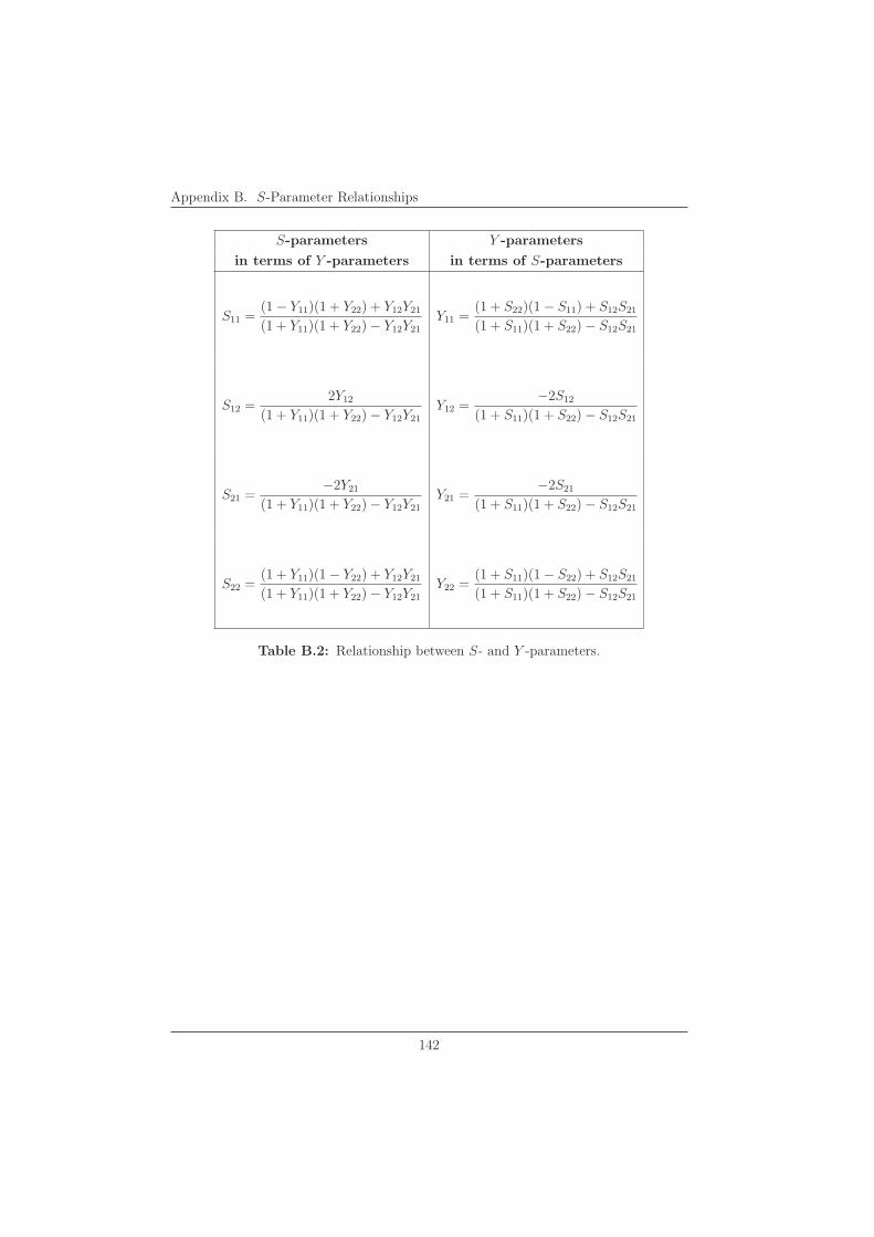
Appendix B. S-Parameter Relationships
S-parameters Y -parameters
in terms of Y -parameters in terms of S-parameters
S11 =(1 − Y11)(1 + Y22) + Y12Y21
(1 + Y11)(1 + Y22) − Y12Y21
Y11 =(1 + S22)(1 − S11) + S12S21
(1 + S11)(1 + S22) − S12S21
S12 =2Y12
(1 + Y11)(1 + Y22) − Y12Y21
Y12 =−2S12
(1 + S11)(1 + S22) − S12S21
S21 =−2Y21
(1 + Y11)(1 + Y22) − Y12Y21
Y21 =−2S21
(1 + S11)(1 + S22) − S12S21
S22 =(1 + Y11)(1 − Y22) + Y12Y21
(1 + Y11)(1 + Y22) − Y12Y21
Y22 =(1 + S11)(1 − S22) + S12S21
(1 + S11)(1 + S22) − S12S21
Table B.2: Relationship between S- and Y -parameters.
142
Appendix C
List of Publications
Proceedings and Journal Papers
C. Urban, Q. T. Zhao, C. Sandow, M. Muller, U. Breuer, S. Mantl, ”Schottky barrier
height modulation by arsenic dopant segregation”, Proceedings of the 9th International
Conference on Ultimate Integration of Silicon, 2008. ULIS 2008, Udine, pp. 151-154.
C. Sandow, J. Knoch, C. Urban, S. Mantl, ”Improving the performance of band-to-
band tunneling transistors by tuning the gate oxide and the dopant concentration”,
Proceedings of the Device Research Conference 2008. DRC 2008, Santa Barbara, pp.
79-80.
M. Muller, Q. T. Zhao, C. Urban, C. Sandow, D. Buca, S. Lenk, S. Estevez, S. Mantl,
”Schottky-barrier height tuning of NiGe/n-Ge contacts using As and P segregation”,
Materials Science and Engineering C, pp. 154-155 (2008).
M. Muller, Q. T. Zhao, C. Urban, C. Sandow, U. Breuer, S. Mantl, ”Schottky-barrier
height tuning of Ni and Pt germanide/n-Ge contacts using dopant segregation.” Pro-
ceedings of the 9th International Conference on Solid-State and Integrated-Circuit Tech-
nology, 2008. ICSICT 2008, Beijing, pp. 153-156.
C. Urban, C. Sandow, Q. T. Zhao, S. Mantl, ”High performance Schottky barrier
MOSFETs on UTB SOI.” Proceedings of the 10th International Conference Ultimate
Integration of Silicon, 2009. ULIS 2009, Aachen, pp. 65-68.
143
Appendix C. List of Publications
Q. T. Zhao, S. B. Mi, C. L. Jia, C. Urban, C. Sandow, S. Habicht, S. Mantl, ”Epitaxial
growth of NiSi2 induced by sulfur segregation at the NiSi2/Si(100) interface.” Journal
of Materials Research, Vol. 24 (2009), 135-139.
C. Urban, M. Emam, C. Sandow, Q.-T. Zhao, A. Fox, J.-P. Raskin, S. Mantl, ”High-
Frequency Performance of dopant-segregated NiSi S/D SOI SB-MOSFETs.” Proceed-
ings of the 39th European Solid-State Device Research Conference, 2009. ESSDERC
2009, Athens, pp. 149-152.
C. Sandow, J. Knoch, C. Urban, Q. T. Zhao, S. Mantl, ”Impact of electrostatics
and doping concentration on the performance of silicon tunnel field-effect transistors.”
Solid-State Electronics, Vol. 53, Issue 10, October 2009, pp. 1126-1129.
C. Urban, C. Sandow, Q.-T. Zhao, J. Knoch, S. Lenk, S. Mantl, ”Systematic study of
Schottky barrier MOSFETs with dopant segregation on thin-body SOI.” Solid-State
Electronics, Vol. 54 (2010), pp. 185-190.
M. Roeckerath, J. M. J. Lopes, E. Durgun Ozben, C. Urban, J. Schubert, S. Mantl, Y.
Jia, D. G. Schlom, ”Investigation of terbium scandate as an alternative gate dielectric
in fully depleted transistors.” Appl. Phys. Lett., Vol. 96 (2010), 013513.
L. Knoll, Q. T. Zhao, S. Habicht, C. Urban, B. Ghyselen, S. Mantl, ”Ultra thin Ni-
silicides with low contact resistance on strained and unstrained silicon.” IEEE Electron
Device Letters, Vol. 31 (2010), Issue 4, pp. 350-352.
C. Urban, M. Emam, C. Sandow, J. Knoch, Q. T. Zhao, J.-P. Raskin, S. Mantl, ”Radio
frequency study of dopant-segregated n-type SB-MOSFETs on thin-body SOI.” IEEE
Electron Device Letters, Vol. 31 (2010), Issue 6, pp. 537-539.
C. Urban, M. Emam, C. Sandow, Q.-T. Zhao, A. Fox, S. Mantl, J.-P. Raskin, ”Small-
signal analysis of high performance p- and n-type SOI SB-MOSFETs with dopant
segregation.” Solid-State Electronics, Vol. 54 (2010), pp. 877-882.
L. Knoll, Q. T. Zhao, S. Habicht, C. Urban, B. Ghyselen, S. Mantl, ”Ultra thin Ni-
silicides with low contact resistance on SOI and strained-SOI.” Proc. of Intern. Conf.
Solid State Dev. Mat., 2009, SSDM 2009, Sendai, pp. 390-391.
144
L. Knoll, Q. T. Zhao, S. Habicht, C. Urban, K. Bourdelle, S. Mantl, ”Formation and
characterization of ultra-thin Ni silicides on strained and unstrained silicon.” Interna-
tional Workshop on Junction Technology, 2010. IWJT 2010, Shanghai, pp. 1-5.
Conference Contributions
C. Urban, Q.-T. Zhao, C. Sandow, M. Muller, S. Mantl, ”Schottky barrier height
modulation of NiSi/Si contacts by dopant segregation.” DPG Tagung 2008, February
25–29th, Berlin, Germany. Oral presentation.
C. Urban, Q.-T. Zhao, C. Sandow, M. Muller, S. Mantl, ”Schottky barrier height en-
gineering of NiSi/Si contacts by dopant segregation.” Material Research Society MRS
2008, March 24–28th., San Francisco, USA. Oral presentation.
C. Urban, Q.-T. Zhao, C. Sandow, U. Breuer, S. Mantl, ”Schottky barrier height
modulation by dopant segregation.” Nanoelectronic Days 2008, May 13–16th, Aachen,
Germany. Poster presentation.
C. Sandow, J. Knoch, C. Urban, S. Mantl, ”Improving the performance of band-to-
band tunneling transistors by tuning the gate oxide and the dopant concentration.”
Device Research Conference DRC 2008, June 23–25th, Santa Barbara, USA. Poster
presentation.
C. Urban, Q.-T. Zhao, C. Sandow, M. Muller, U. Breuer, S. Mantl, ”Schottky bar-
rier height modulation by arsenic dopant segregation.” 9th Conference on Ultimate
Integration on Silicon ULIS 2008, March 12–14th, Udine, Italy. Poster presentation.
C. Urban, Q. T. Zhao, C. Sandow, S. Lenk, S. Mantl, ”Systematic study of SOI SB-
MOSFETs with dopant segregation.” EUROSOI 2009, January 19–21th, Gothenburg,
Sweden. Oral presentation.
C. Urban, Q. T. Zhao, C. Sandow, M. Muller, S. Mantl, ”Schottky barrier height
tuning using Sb segregation.” Materials for advanced Metallization MAM 2009, March
8–9th, Grenoble, France. Oral presentation.
145
Appendix C. List of Publications
C. Urban, C. Sandow, Q.-T. Zhao, S. Mantl, ”High performance Schottky barrier MOS-
FETs on UTB SOI.” 10th Conference on Ultimate Integration on Silicon ULIS 2009,
March 18–20th, Aachen, Germany. Oral presentation.
S. F. Feste, C. Urban, J. Knoch, Q. T. Zhao, D. Buca, U. Breuer, S. Mantl, ”Inves-
tigation of arsenic dopant segregation layers for scaled Schottky-barrier MOSFETs.”
The European Material Research Society E-MRS Spring Meeting 2009, June 08–12th,
Strasbourg, France. Poster presentation.
C. Urban, M. Emam, C. Sandow, Q.-T. Zhao, A. Fox, J.-P. Raskin, S. Mantl, ”High-
frequency performance of dopant-segregated NiSi S/D SOI SB-MOSFETs.” 39th Eu-
ropean Solid-State Device Reasearch Conference ESSDERC 2009, September 14–18th,
Athens, Greece. Oral presentation.
L. Knoll, Q. T. Zhao, S. Habicht, C. Urban, B. Ghyselen, S. Mantl, ”Ultra thin Ni-
silicides with low contact resistance on SOI and strained-SOI.” Intern. Conf. Solid
State Dev. Mat., 2009, SSDM 2009, Sendai, October 7–9th, Sendai, Japan. Poster
presentation.
146
Appendix D
Acknowledgement
It is a pleasure for me to thank everybody who contributed to this thesis by engagement,
assistance, advice or in various other ways.
• First of all, I would like to thank Prof. Dr. S. Mantl for giving me the opportunity
to work in his research group on an excellent topic and for his continuous interest
and help during the work on the SB-MOSFETs.
• Special thanks goes to Prof. Dr. M. Morgenstern for undertaking the Koreferat
of this work.
• I am also indebted to my supervisor Dr. Q. T. Zhao and my former supervi-
sor Prof. Dr. J. Knoch who helped me during various pathbreaking discussions.
Thank you, Qing-Tai, for providing me the background of semiconductor pro-
cessing and especially for the introduction in the silicide technology. Joachim, I
enjoyed several discussions which took place mainly by phone and for the oppor-
tunity to use the LPCVD of your institute at the TU Dortmund.
• My dearest thanks goes to Dipl.-Phys. C. Sandow who started his PhD thesis
at the same time as me. In the past few years we got very good friends and I
enjoyed our private conversations a lot. Our fruitful discussions about cleanroom
processing, MOSFETs, SB-MOSFETs, T-FETs, measurement techniques,... con-
tributed highly to this thesis. Moreover, I would like to thank you for introducing
me in MATLAB programming which simplified many extractions. Christian, it
was a great pleasure working together with you and sharing your experience and
enthusiasm.
• For great collaboration I would like to express my sincere thanks to Prof. Dr. J.-
P. Raskin and Dipl.-Ing. M. Emam from the Universite catholique de Louvain.
147
Appendix D. Acknowledgement
Particularly, I thank you, Jean-Pierre, for providing me the possibility to perform
mircowave measurements in your institute and for fertile debates. Mostafa, I
enjoyed the two very productive measurements campaigns with you and I am very
glad that we did the RF characterization together. I learned many things about
RF measurements, which were inaccessible for me before my stays in Louvain-la-
Neuve.
• Moreover, I would like to thank all my roommates, Dipl.-Phys. M. Muller, Dipl.-
Phys. W. Heiermann and Dipl.-Phys. M. Schmidt, for an enjoyable atmosphere
in our office. Marcel, I gladly remember our discussions about the extraction of
Schottky barrier heights.
• Dr. J. Schubert, Dr. M. Rockerath for numerous discussions and private conver-
sations and Dipl.-Phys. E. Durgun-Ozben for the extraction of the interface trap
density.
• W. Michelsen, A. Dahmen, S. Lenk and D. Meertens for many ion implantations,
TEM images and FIB-preparations.
• All other group members of IBN1-IT with whom I had the pleasure to work.
• Dipl.-Ing. A. Fox and Prof. Dr. M. Marso for discussions about the RF layout
of the transistors and the first S-parameter measurements as well as help during
low-temperature measurements.
• Dr. S. Trellenkamp and Dr. V. Guzenko for e-beam writing and M. Nonn for the
fabrication of the masks for optical lithography.
• Dr. U. Breuer for the SIMS analysis of the Schottky diodes and Dr. G. Mussler
for the XRR measurements.
• Dr. T. Stockmanns for giving me access to the automatic measurement setup of
the Institute for Nuclear Physics.
• Dipl-Ing. T. Mollenhauer of AMO GmbH for ICP etching of the gate stacks
• The cleanroom staff under Dipl. Ing. A. Steffens’ leadership for the excellent co-
operation and valuable advice. In particular, H. Wingens for many metallizations
performed with nearly no waiting time and with greatest care, K. H. Deussen for
numerous TEOS and poly-Si depositions, J. Mohr for her help if it was needed
urgently, S. Bunte for wafer cutting, Dipl.-Ing. H.-P. Bochem for introducing me
to the SEM and J. Muller for introducing me to many machines and for helping
me with various problems in the cleanroom.
148
• Last but not least I thank my wife Susanna ♥, my parents and my sister for their
love, patience, support, understanding and all the time they let me off instead of
spending it with them during the last few years.
149
Appendix D. Acknowledgement
150
Appendix E
Curriculum Vitae
PERSONAL DETAILS
Name: Urban
First names: Christoph Johannes
Date of birth: September 10th, 1979
Place of birth: Paderborn, Germany
Nationality: German
EDUCATION AND QUALIFICATIONS
1999 Abitur (A-level), Reismann Gymnasium Paderborn
08/1999 – 06/2000 Civilian service as paramedic, Malteser Hilfsdienst e. V.
10/2000 – 09/2005 Study of Physics at the University of Paderborn
09/2004 – 09/2005 University of Paderborn, Department of Physics,
Student assistant with Prof. Dr. G. Wortmann
Diploma thesis: ”Magnetismus und Gitterdynamik
in SrFeO2.5+x und verwandten Systemen: Temperatur-
abangige Untersuchungen mit 57Fe-Mossbauereffekt
und kernresonanter Streuung von Synchrotronstrahlung”
09/2005 Diplom in Physics at the University of Paderborn
10/2005 – 01/2006 University of Paderborn, Department of Physics,
Scientific employee with Prof. Dr. G. Wortmann
04/2006 – 03/2010 Research Center Julich, Institute for Bio- and Nanosystems 1,
PhD Student with Prof. Dr. S. Mantl
151
Schriften des Forschungszentrums Jülich Reihe Information / Information
1. Ferrocenes as Potential Building Blocks for Molecular Electronics Self-Assembly and Tunneling Spectroscopy by L. Müller-Meskamp (2008), 153 pages ISBN: 978-3-89336-509-8
2. Magnetic Proximity Effects in Highly-ordered Transition Metal Oxide Heterosystems studied by Soft x-Ray Photoemission Electron Microscopy by I. P. Krug (2008), XX, 180 pages ISBN: 978-3-89336-521-0
3. Seltenerd-basierte ternäre Oxide als alternative Gatedielektrika von J. M. Roeckerath (2008), 148 Seiten ISBN: 978-3-89336-543-2
4. Strominduzierte Magnetisierungsdynamik in einkristallinen Nanosäulen von R. Lehndorff (2009), I, 86 Seiten ISBN: 978-3-89336-564-7
5. Magnetization Dynamics in Magnetically Coupled Heterostructures von A. Kaiser (2009), X, 121 pages ISBN: 978-3-89336-577-7
6. Resistive switching in Pt/TiO2/PT by D. S. Jeong (2009), vii, 133 pages ISBN: 978-3-89336-579-1
7. Electromechanical Force Microscopy and Tip-Enhanced Raman Spectroscopy for Polar Oxide Nanoparticles by S. Röhrig (2009), vi, 114 pages ISBN: 978-3-89336-600-2
8. Investigation of resistive switching in barium strontium titanate thin films for memory applications by W. Shen (2010), 114 pages ISBN: 978-3-89336-608-8
9. Nanostrukturierte Metallelektroden zur funktionalen Kopplung an neuronale Zellen von D. Brüggemann (2010), vii, 160 Seiten ISBN: 978-3-89336-627-9
10. Integration of resistive switching devices in crossbar structures by Chr. Nauenheim (2010), XII, 142 pages ISBN: 978-3-89336-636-1
Schriften des Forschungszentrums Jülich Reihe Information / Information
11. Correlation between Raman spectroscopy and electron microscopy on individual carbon nanotubes and peapods by C. Spudat (2010). xiv, 125 pages ISBN: 978-3-89336-648-4
12. DC and RF Characterization of NiSi Schottky Barrier MOSFETs with Dopant Segregation by C. J. Urban (2010), iv, 151 pages ISBN: 978-3-89336-644-6

Info
rmat
ion
12 Mitg
lied
der
Hel
mho
ltz-G
emei
nsch
aft
DC and RF Characterization of NiSi Schottky Barrier MOSFETs with Dopant Segregation
Christoph Johannes Urban
Chr
isto
ph Jo
hann
es U
rban
DC
and
RF
Cha
ract
eriz
atio
n of
Nis
i SB-
MO
SFET
s
Information / InformationBand / Volume 12ISBN 978-3-89336-644-6