Current conduction mechanism in Al/pSi Schottky barrier diodes with native insulator layer at low...
6
Current conduction mechanism in Al/p-Si Schottky barrier diodes with native insulator layer at low temperatures S ¸. Altındal a, * , H. Kanbur a , D.E. Yıldız a , M. Parlak b a Physics Department, Faculty of Arts and Sciences, Gazi University, 06500 Ankara, Turkey b Physics Department, Middle East Technical University, 06531 Ankara, Turkey Received 25 April 2006; received in revised form 10 November 2006; accepted 11 November 2006 Available online 13 December 2006 Abstract The forward bias current–voltage (I–V) characteristics of Al/p-Si (MS) Schottky diodes with native insulator layer were measured in the temperature range of 80–300 K. The obtained zero bias barrier height F B0 (I–V), ideality factor (n) and series resistance (R s ) determined by using thermionic emission (TE) mechanism show strong temperature dependence. There is a linear correlation between the F B0 (I–V) and n because of the inhomogeneties in the barrier heights (BHs). Calculated values from temperature dependent I–V data reveal an unusual behaviour such that the F B0 decreases, as the n and R s values are increasing with decreasing absolute temperature, and these changes are more pronounced especially at low temperatures. Such temperature dependence of BH is contradictory with the reported negative temperature coefficient of the barrier height. In order to explain this behaviour we have reported a modification in the expression reverse saturation current I o including the n and the tunnelling factor (aX 1/2 d) estimated to be 15.5. Therefore, corrected effective barrier height F bef. (I–V) versus temperature has a negative temperature coefficients (a = 2.66 10 4 eV/K) and it is in good agreement with negative temperature coefficients (a = 4.73 10 4 eV/K) of Si band gap. In addition, the temperature dependent energy distribution of interface states density N ss profiles was obtained from the forward bias I–V measurements by taking into account the bias dependence of the F e and n. The forward bias I–V characteristics confirm that the distribution of N ss , R s and interfacial insulator layer are important parameters that the current conduction mechanism of MS Schottky diodes. # 2006 Elsevier B.V. All rights reserved. PACS : 73.30.+y: 73.40.Qv: 73.40.Ns Keywords: Series resistance; Interface states; Native insulator layer; Conduction mechanisms; I–V characteristics 1. Introduction The interface properties, current conduction mechanisms and some structural parameters of metal-semiconductor (MS) or metal-insulator-semiconductor (MIS) Schottky diodes have been subject of both experimental and theoretical studies in the past decades [1–17], but very little experimental information is available on Schottky barrier formation and interface states N ss between metal and semiconductor. Also the series resistance (R s ) of MS Schottky diodes and a thin insulator layer at MS interface are an important parameters that affect the behaviour of MS Schottky diodes [1,3,8,13– 18]. There are a lot of methods for the measurements of R s , but the theoretical expression of R s is still un-clarified and has not been clearly disclosed in literature. The effective tunnelling barriers of thin insulator (SiO 2 ) layer on Si have been studies by several authors [1–7]. In MIS structures with sufficiently thick interfacial insulator layer (d 25 A ˚ ), N ss are equilibrium with semiconductor and they cannot interact with the metal [1,8,9]. However, the formation and characteriza- tion of interfacial insulator/oxide layers such as SiO 2 , SnO 2 and Si 3 N 4 on Si and their effects still remain a basic problem. Therefore, MS Schottky diodes with native or deposited insulator layer have been gained increasing importance due to their importance in semiconductor technology. Usually, the forward bias current–voltage (I–V) characteristics are linear in the semi-logarithmic scale at low voltages but deviate considerably from linearity due to the effect of device parameters, such as the R s , when the applied voltage is sufficiently large [1,9–12]. www.elsevier.com/locate/apsusc Applied Surface Science 253 (2007) 5056–5061 * Corresponding author. Fax: +90 312 212 2279. E-mail address: [email protected] (S ¸. Altındal). 0169-4332/$ – see front matter # 2006 Elsevier B.V. All rights reserved. doi:10.1016/j.apsusc.2006.11.015
-
Upload
independent -
Category
Documents
-
view
5 -
download
0
Transcript of Current conduction mechanism in Al/pSi Schottky barrier diodes with native insulator layer at low...
www.elsevier.com/locate/apsusc
Applied Surface Science 253 (2007) 5056–5061
Current conduction mechanism in Al/p-Si Schottky barrier diodes
with native insulator layer at low temperatures
S. Altındal a,*, H. Kanbur a, D.E. Yıldız a, M. Parlak b
a Physics Department, Faculty of Arts and Sciences, Gazi University, 06500 Ankara, Turkeyb Physics Department, Middle East Technical University, 06531 Ankara, Turkey
Received 25 April 2006; received in revised form 10 November 2006; accepted 11 November 2006
Available online 13 December 2006
Abstract
The forward bias current–voltage (I–V) characteristics of Al/p-Si (MS) Schottky diodes with native insulator layer were measured in the
temperature range of 80–300 K. The obtained zero bias barrier height FB0(I–V), ideality factor (n) and series resistance (Rs) determined by using
thermionic emission (TE) mechanism show strong temperature dependence. There is a linear correlation between the FB0(I–V) and n because of
the inhomogeneties in the barrier heights (BHs). Calculated values from temperature dependent I–V data reveal an unusual behaviour such that the
FB0 decreases, as the n and Rs values are increasing with decreasing absolute temperature, and these changes are more pronounced especially at
low temperatures. Such temperature dependence of BH is contradictory with the reported negative temperature coefficient of the barrier height. In
order to explain this behaviour we have reported a modification in the expression reverse saturation current Io including the n and the tunnelling
factor (aX1/2d) estimated to be 15.5. Therefore, corrected effective barrier height Fbef.(I–V) versus temperature has a negative temperature
coefficients (a = �2.66 � 10�4 eV/K) and it is in good agreement with negative temperature coefficients (a = �4.73 � 10�4 eV/K) of Si band
gap. In addition, the temperature dependent energy distribution of interface states density Nss profiles was obtained from the forward bias I–V
measurements by taking into account the bias dependence of the Fe and n. The forward bias I–V characteristics confirm that the distribution of Nss,
Rs and interfacial insulator layer are important parameters that the current conduction mechanism of MS Schottky diodes.
# 2006 Elsevier B.V. All rights reserved.
PACS : 73.30.+y: 73.40.Qv: 73.40.Ns
Keywords: Series resistance; Interface states; Native insulator layer; Conduction mechanisms; I–V characteristics
1. Introduction
The interface properties, current conduction mechanisms
and some structural parameters of metal-semiconductor (MS)
or metal-insulator-semiconductor (MIS) Schottky diodes
have been subject of both experimental and theoretical
studies in the past decades [1–17], but very little experimental
information is available on Schottky barrier formation and
interface states Nss between metal and semiconductor. Also
the series resistance (Rs) of MS Schottky diodes and a thin
insulator layer at MS interface are an important parameters
that affect the behaviour of MS Schottky diodes [1,3,8,13–
18]. There are a lot of methods for the measurements of Rs,
* Corresponding author. Fax: +90 312 212 2279.
E-mail address: [email protected] (S. Altındal).
0169-4332/$ – see front matter # 2006 Elsevier B.V. All rights reserved.
doi:10.1016/j.apsusc.2006.11.015
but the theoretical expression of Rs is still un-clarified and
has not been clearly disclosed in literature. The effective
tunnelling barriers of thin insulator (SiO2) layer on Si have
been studies by several authors [1–7]. In MIS structures with
sufficiently thick interfacial insulator layer (d � 25 A), Nss are
equilibrium with semiconductor and they cannot interact with
the metal [1,8,9]. However, the formation and characteriza-
tion of interfacial insulator/oxide layers such as SiO2, SnO2
and Si3N4 on Si and their effects still remain a basic problem.
Therefore, MS Schottky diodes with native or deposited
insulator layer have been gained increasing importance due to
their importance in semiconductor technology. Usually, the
forward bias current–voltage (I–V) characteristics are linear
in the semi-logarithmic scale at low voltages but deviate
considerably from linearity due to the effect of device
parameters, such as the Rs, when the applied voltage is
sufficiently large [1,9–12].
S. Altındal et al. / Applied Surface Science 253 (2007) 5056–5061 5057
Experimental results, especially only at room temperature,
do not give detailed information about conduction mechanisms
or the nature of barrier formation at the MS or MIS Schottky
diodes. Therefore, the current–voltage characteristics of the
samples have been studied as a function of temperature in the
temperature range of 80–300 K. Since, the temperature
dependence of the I–V characteristics allows us to understand
different aspect of conduction mechanism. Generally, the
thermionic emission theory (TE) is used to extract the
parameters of Schottky barrier diodes (SBDs) [8,9], and the
ideality factor is expected to be close to unity, similar to that
observed at uniform SBDs. However, analysis of the I–V
characteristics of SBDs based on TE theory usually reveals an
abnormal decreasing in the barrier height (BH) and increasing
in the ideality factor (n) with decreasing temperature, which
leads to non-linearity in the ln (Io/T2) versus 1/T plots [13–17].
The non-linear behaviour of I–V characteristics of MS and MIS
type Schottky diodes at low temperatures has been attributed to
the spatial variation of barrier heights (BHs).
In our previous work [18], the effects of the interface states
(Nss) and excess capacitance (Co) causing non-ideal behavior
electrical characteristics of MIS structure were investigated and
also a systematic investigation on the frequency dependence of
the electrical properties of these structures were carried out at
room temperature. It was found that the characteristics of MIS
structures have been controlled by the interfacial insulator layer
and Nss, and they are responsible for the non-ideal behavior of
I–V, C (V,f) and G (V,f) characteristics. Therefore, in this work,
the electrical characteristics of Al/SiO2/p-Si Schottky diodes
have been studied in the temperature range 80–300 K. We have
reported a modification in the expression of reverse saturation
current Io by including the ideality factor n and tunnelling
parameter (ax1/2d). The temperature dependent energy
distribution profile of interface states Nss was obtained from
the forward bias I–V characteristics by taking into account both
the bias dependence of the FB, n and Rs. To extract the values
of the real Rs, FB and n of Al/SiO2/p-Si (MIS) structures,
Cheung’s method [32] has been applied in the studied
temperature range.
2. Experimental procedure
The metal-semiconductor (Al/p-Si) Schottky diodes used in
this study were fabricated by using p-type (boron-doped) single
crystal silicon wafer with <1 0 0> surface orientation, having
thickness of 280 mm, 200 diameter and 8 (V cm) resistivity. For
the fabrication process, Si wafer was degreased in organic
solvent of CHClCCl2, CH3COCH3 and CH3OH, etched in a
sequence of H2SO4 and H2O2, 20% HF, a solution of
6HNO3:1HF:35H2O, 20% HF and finally quenched in de-
ionised water of resistivity of 18 (MV cm) for a prolonged time.
High purity (99.999%) aluminium with a thickness of�2000 A
was thermally evaporated from the tungsten filament onto the
whole backside of half wafer at a pressure of �2 � 10�5 Torr.
The ohmic contacts were prepared by sintering the evaporated
Al back contact at 650 8C for 60 min under dry nitrogen flow at
rate of 2 l/min. This process served to sinter the aluminium on
the upper surface of the Si wafer. After deposition of ohmic
contact, the front surface of the Si wafer was exposed to air in
sterile glass box for two years at room temperature. The front
rectifier contacts were produced by the evaporation of 2000 A
thick aluminium dots of �1 mm in diameter onto the Si wafer.
The thickness of metallic layer and the deposition rate were
monitored with the help of Inficon XTM/2 thickness monitor.
By this way, metal-semiconductor (MS) diode with a thin
interfacial insulator layer (SiO2) was fabricated on p-type Si.
The interfacial layer thickness was estimated to be about 32 A
from the oxide capacitance measurement in the strong
accumulation region at high frequency (1 MHz). I–V measure-
ments were performed by using a Keithley 220 current source
and a Keithley 614 electrometer. The sample temperature was
always monitored by means of a copper-constant thermocouple
and a Lakeshore 321 auto-tuning temperature controller
with sensitivity better than � 0.1 K. All measurements were
carried out with the help of a microcomputer through an
IEEE-488 ac/dc converter card.
3. Experimental results and discussion
We fabricated 46 Schottky barrier diodes (Al/p-Si) with a
native insulator layer (SiO2) on a quarter of the p-type (boron
doped) single crystal silicon wafer having thickness of 280 mm
with �8 V cm resistivity. The values of calculated basic
electrical parameters for each device were almost the same with
each other. Therefore, we have introduced only one Schottky
diode as a typical device in this work. When a MS contact with
an interfacial insulator layer and series resistance Rs is
considered, the current through a Schottky diode can be given
by [8,9]
I ¼ I0 exp
�qðV � IRsÞ
nkT
��1� exp
��qðV � IRsÞ
kT
��(1)
where I0 is the reverse saturation current and is equal to
I0 ¼ AA�T2 exp
�� qFB0
kT
�(2)
where FB0 is the zero bias barrier height, A is the diode area, A*
is the effective Richardson constant and equals to 32 A/cm2 K2
for p-type Si, n is an ideality factor, Rs is the series resistance of
diode, T the absolute temperature in Kelvin, k the Boltzmann
constant, and V is the applied voltage. The semi-logarithmic
forward bias I–V plots of the Al/SiO2/p-Si (MIS) Schottky
diodes in the temperature range of 80–300 K are shown in
Fig. 1. As can be seen in Fig. 1, the downward curvature in the
I–V characteristics at high forward bias values is attributed to a
continuum of surface states (Nss), which are in equilibrium with
the semiconductor, apart from the effect of Rs. While the Rs, is
significant especially in the downward curvature of the forward
bias I–V characteristics, the Nss is effective in both inversion
and depletion range and their distribution profile changes from
region to region in the band gap.
The Io values were obtained by extrapolating the linear
portion of the forward bias ln (I)–V plot to the intercept point on

Fig. 1. The semi-logarithmic forward bias I–V plots of the Al/SiO2/p-Si (MIS)
Schottky diode at various temperatures.
Fig. 2. Temperature dependence of FBo, FBef., and n obtained from forward
bias I–V characteristics for Al/SiO2/p-Si (MIS) Schottky diode.
S. Altındal et al. / Applied Surface Science 253 (2007) 5056–50615058
the current axis at zero bias (V = 0) and the FB0 values were
calculated by using Eq. (2). The values ideality factor n were
calculated from the slope of the ln (I)–V graph in the linear
region and can be written using Eq. (1) as;
n ¼ q
kT
�dðV � IRsÞ
dðlnðIÞÞ
�(3)
The changes in Io, n and FB0 with temperature are given in
Table 1. As seen from Table 1., the calculated values of Io, n and
FB0 were found to be as strongly temperature dependent. The
experimental values of Io, n and FB0 for the Al/SiO2/p-Si (MIS)
Schottky diode change from 6.9 � 10�15 A, 6.46, and 0.28 eV
(at 80 K) to 1.3 � 10�8 A, 3.40, and 0.73 eV (at 300 K). Such a
Table 1
Temperature dependent values of various parameters determined from forward bias
80–300 K
T (K) Io (A) n FB0 (eV) FBef. (eV)
80 6.90E�15 6.46 0.28 1.00
100 3.49E�13 6.05 0.31 0.99
125 3.92E�12 5.38 0.37 0.99
150 2.25E�11 4.82 0.43 0.98
175 1.69E�10 4.63 0.47 0.97
200 6.57E�10 4.37 0.52 0.97
225 1.84E�09 4.11 0.57 0.96
250 3.98E�09 3.85 0.63 0.95
275 5.84E�09 3.54 0.68 0.95
300 1.30E�08 3.40 0.73 0.94
behaviour of ideality factor has been attributed to particular
distribution of interface states and insulator layer between
metal and semiconductor [1,3,19].
These values of FB0 calculated from forward bias I–V
characteristics have shown an unusual behaviour such that it
increases with increasing temperature. As can be seen from
Fig. 2, temperature dependence of FB0 shows ambiguous
behaviour as compared with the reported negative temperature
coefficient of the Schottky barrier height. The values of ideality
factor n are found to be increasing in between 3.40 and 6.46,
while the FB0 decreases with decreasing temperature (Fig. 2.).
The high values of the ideality factor show that there is a
deviation from TE theory in the current conduction mechanism.
Moreover, the ideality factor varies almost linearly with the
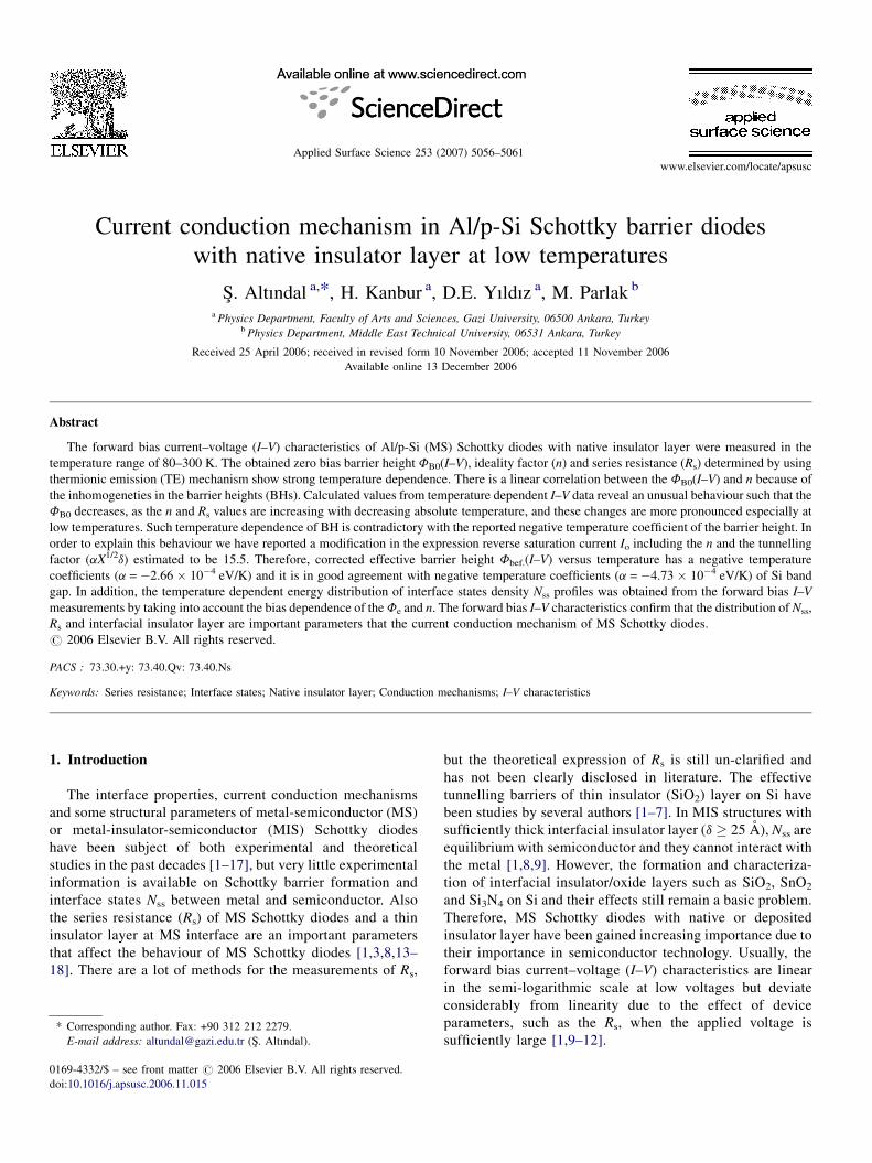
inverse temperature as in Fig. 3 and can be expressed as;
nðTÞ ¼ no þTo
T(4)
where the no and To are constant with the values 2.27 and
381.7 K, respectively. The temperature dependence of n sug-
gests that the current conduction mechanism is controlled by
the thermionic field emission (TFE) [20,21]. This implies that
in these samples the effects of the surface states (Nss) are more
pronounced because of the spatial distribution of the insulator
I–V characteristics of Al/SiO2/p-Si Schottky diode in the temperature range of
Rs(dV/d ln I) (V) Rs(H(I)) (V) Nss (eV�1 cm�2)
247 399 3.58 � 1013
231 317 3.32 � 1013
280 410 2.88 � 1013
271 542 2.51 � 1013
443 623 2.38 � 1013
580 803 2.21 � 1013
727 871 2.04 � 1013
891 982 1.87 � 1013
1078 1172 1.67 � 1013
1310 1399 1.57 � 1013
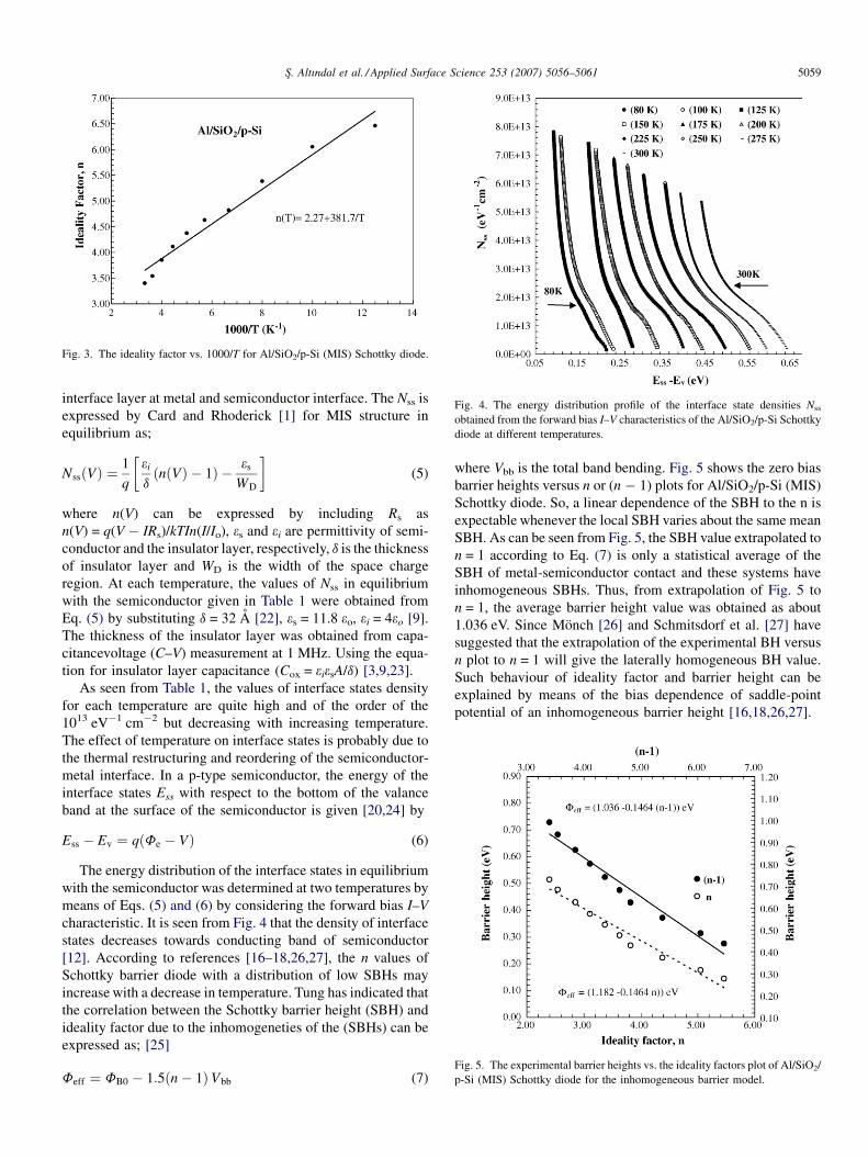
Fig. 3. The ideality factor vs. 1000/T for Al/SiO2/p-Si (MIS) Schottky diode.
Fig. 4. The energy distribution profile of the interface state densities Nss
obtained from the forward bias I–V characteristics of the Al/SiO2/p-Si Schottky
diode at different temperatures.
Fig. 5. The experimental barrier heights vs. the ideality factors plot of Al/SiO2/
p-Si (MIS) Schottky diode for the inhomogeneous barrier model.
S. Altındal et al. / Applied Surface Science 253 (2007) 5056–5061 5059
interface layer at metal and semiconductor interface. The Nss is
expressed by Card and Rhoderick [1] for MIS structure in
equilibrium as;
NssðVÞ ¼1
q
�ei
dðnðVÞ � 1Þ � es
WD
�(5)
where n(V) can be expressed by including Rs as
n(V) = q(V � IRs)/kTIn(I/Io), es and ei are permittivity of semi-
conductor and the insulator layer, respectively, d is the thickness
of insulator layer and WD is the width of the space charge
region. At each temperature, the values of Nss in equilibrium
with the semiconductor given in Table 1 were obtained from
Eq. (5) by substituting d = 32 A [22], es = 11.8 eo, ei = 4eo [9].
The thickness of the insulator layer was obtained from capa-
citancevoltage (C–V) measurement at 1 MHz. Using the equa-
tion for insulator layer capacitance (Cox = eiesA/d) [3,9,23].
As seen from Table 1, the values of interface states density
for each temperature are quite high and of the order of the
1013 eV�1 cm�2 but decreasing with increasing temperature.
The effect of temperature on interface states is probably due to
the thermal restructuring and reordering of the semiconductor-
metal interface. In a p-type semiconductor, the energy of the
interface states Ess with respect to the bottom of the valance
band at the surface of the semiconductor is given [20,24] by
Ess � Ev ¼ qðFe � VÞ (6)
The energy distribution of the interface states in equilibrium
with the semiconductor was determined at two temperatures by
means of Eqs. (5) and (6) by considering the forward bias I–V
characteristic. It is seen from Fig. 4 that the density of interface
states decreases towards conducting band of semiconductor
[12]. According to references [16–18,26,27], the n values of
Schottky barrier diode with a distribution of low SBHs may
increase with a decrease in temperature. Tung has indicated that
the correlation between the Schottky barrier height (SBH) and
ideality factor due to the inhomogeneties of the (SBHs) can be
expressed as; [25]
Feff ¼ FB0 � 1:5ðn� 1ÞVbb (7)
where Vbb is the total band bending. Fig. 5 shows the zero bias
barrier heights versus n or (n � 1) plots for Al/SiO2/p-Si (MIS)
Schottky diode. So, a linear dependence of the SBH to the n is
expectable whenever the local SBH varies about the same mean
SBH. As can be seen from Fig. 5, the SBH value extrapolated to
n = 1 according to Eq. (7) is only a statistical average of the
SBH of metal-semiconductor contact and these systems have
inhomogeneous SBHs. Thus, from extrapolation of Fig. 5 to
n = 1, the average barrier height value was obtained as about
1.036 eV. Since Monch [26] and Schmitsdorf et al. [27] have
suggested that the extrapolation of the experimental BH versus
n plot to n = 1 will give the laterally homogeneous BH value.
Such behaviour of ideality factor and barrier height can be
explained by means of the bias dependence of saddle-point
potential of an inhomogeneous barrier height [16,18,26,27].
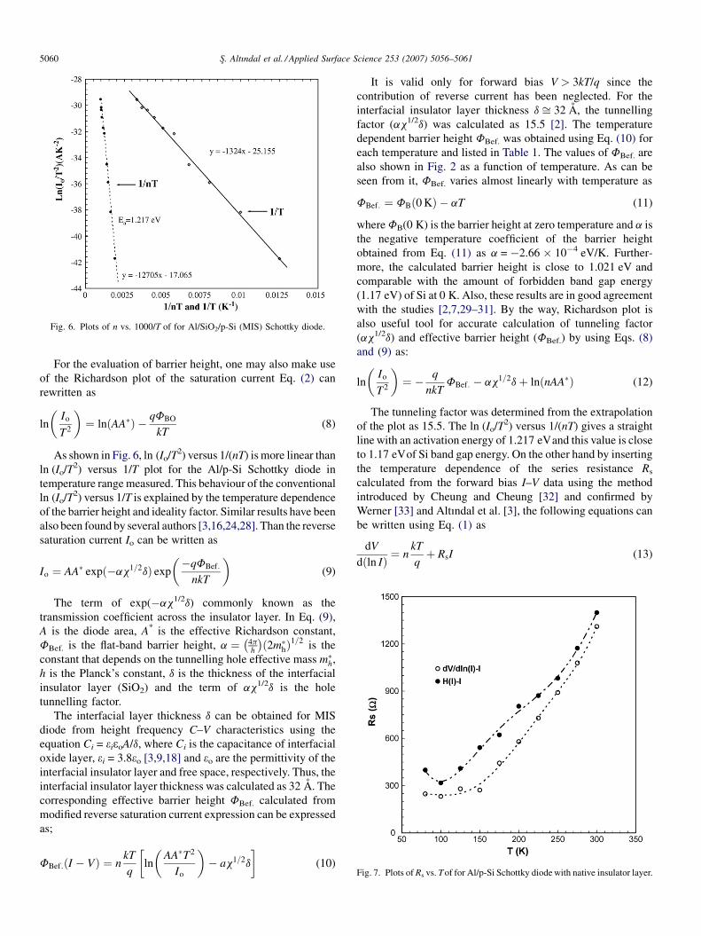
Fig. 6. Plots of n vs. 1000/T of for Al/SiO2/p-Si (MIS) Schottky diode.
Fig. 7. Plots of Rs vs. Tof for Al/p-Si Schottky diode with native insulator layer.
S. Altındal et al. / Applied Surface Science 253 (2007) 5056–50615060
For the evaluation of barrier height, one may also make use
of the Richardson plot of the saturation current Eq. (2) can
rewritten as
ln
�Io
T2
�¼ lnðAA�Þ � qFBO
kT(8)
As shown in Fig. 6, ln (Io/T2) versus 1/(nT) is more linear than
ln (Io/T2) versus 1/T plot for the Al/p-Si Schottky diode in
temperature range measured. This behaviour of the conventional
ln (Io/T2) versus 1/T is explained by the temperature dependence
of the barrier height and ideality factor. Similar results have been
also been found by several authors [3,16,24,28]. Than the reverse
saturation current Io can be written as
Io ¼ AA� expð�ax1=2dÞ exp
��qFBef:
nkT
�(9)
The term of exp(�ax1/2d) commonly known as the
transmission coefficient across the insulator layer. In Eq. (9),
A is the diode area, A* is the effective Richardson constant,
FBef. is the flat-band barrier height, a ¼ 4ph
� �ð2m�hÞ
1=2is the
constant that depends on the tunnelling hole effective mass m�h,
h is the Planck’s constant, d is the thickness of the interfacial
insulator layer (SiO2) and the term of ax1/2d is the hole
tunnelling factor.
The interfacial layer thickness d can be obtained for MIS
diode from height frequency C–V characteristics using the
equation Ci = eieoA/d, where Ci is the capacitance of interfacial
oxide layer, ei = 3.8eo [3,9,18] and eo are the permittivity of the
interfacial insulator layer and free space, respectively. Thus, the
interfacial insulator layer thickness was calculated as 32 A. The
corresponding effective barrier height FBef. calculated from
modified reverse saturation current expression can be expressed
as;
FBef:ðI � VÞ ¼ nkT
q
�ln
�AA�T2
Io
�� ax1=2d
�(10)
It is valid only for forward bias V > 3kT/q since the
contribution of reverse current has been neglected. For the
interfacial insulator layer thickness d ffi 32 A, the tunnelling
factor (ax1/2d) was calculated as 15.5 [2]. The temperature
dependent barrier height FBef. was obtained using Eq. (10) for
each temperature and listed in Table 1. The values of FBef. are
also shown in Fig. 2 as a function of temperature. As can be
seen from it, FBef. varies almost linearly with temperature as
FBef: ¼ FBð0 KÞ � aT (11)
where FB(0 K) is the barrier height at zero temperature and a is
the negative temperature coefficient of the barrier height
obtained from Eq. (11) as a = �2.66 � 10�4 eV/K. Further-
more, the calculated barrier height is close to 1.021 eV and
comparable with the amount of forbidden band gap energy
(1.17 eV) of Si at 0 K. Also, these results are in good agreement
with the studies [2,7,29–31]. By the way, Richardson plot is
also useful tool for accurate calculation of tunneling factor
(ax1/2d) and effective barrier height (FBef.) by using Eqs. (8)
and (9) as:
ln
�Io
T2
�¼ � q
nkTFBef: � ax1=2dþ lnðnAA�Þ (12)
The tunneling factor was determined from the extrapolation
of the plot as 15.5. The ln (Io/T2) versus 1/(nT) gives a straight
line with an activation energy of 1.217 eVand this value is close
to 1.17 eVof Si band gap energy. On the other hand by inserting
the temperature dependence of the series resistance Rs
calculated from the forward bias I–V data using the method
introduced by Cheung and Cheung [32] and confirmed by
Werner [33] and Altındal et al. [3], the following equations can
be written using Eq. (1) as
dV
dðln IÞ ¼ nkT
qþ RsI (13)
ce Science 253 (2007) 5056–5061 5061
H
�I
�¼ V � n
kT
qln
�I
AA�T2
�nFB þ RsI (14)
where FB is the barrier height obtained from data of downward
curvature region in the forward bias I–V characteristics. The
values of Rs versus T calculated from Eq. (13) and Eq. (14) are
shown in Table 1 and Fig. 7. It shows that the series resistance
increases with increasing temperature as could be expected for
semiconductors in the studied temperature range where there is
no freezing out of carrier and also non-negligible below
�125 K. Such temperature dependence of Rs was observed
experimentally for all Al/p-Si Schottky diodes with good
quality backside ohmic contact [34]. Also, a similar result
was obtained recently by simulations forward I–V curves of
Schottky diode [34,35].
4. Conclusion
The forward bias I–V characteristics of Al/p-Si Schottky
diode with native insulator layer were measured in the
temperature range of 80–300 K. While the zero bias barrier
height FB0 and series resistance Rs increases, the ideality factor
n decreases with an increase in temperature, the changes are
quite significant at low temperatures. This variation of Rs with
the temperature can be expected for semiconductors in the
temperature region where there is no freezing out behaviour of
carrier. Furthermore, the forward bias ln (I)–V plots show that
the all plots intersect the almost same common crossing-point
at certain bias voltage and this common voltage point is
temperature independent. This behaviour of the crossing of I–V
curves seems to ambiguous as compared with the conventional
behaviour of Schottky barrier diodes.
We have reported a modification, by the inclusion both of n
and ax1/2d in the expression of saturation current (Io) to explain
the experimental I–V characteristics of Al/p-Si Schottky diode.
The validity of including n and ax1/2d in the expression of Io are
demonstrated by comparing the corrected values of barrier
height FBef. and by checking the temperature dependence of
barrier height against that of energy band gap Eg. In addition,
the temperature dependence of Nss profiles was obtained from
the forward bias I–V measurements by taking into account the
bias dependence of the Fe and n. The forward bias I–V
characteristics confirm that the distribution of Nss, Rs and
interfacial insulator layer are important parameters in the
current conduction mechanism of MS Schottky diodes.
S. Altındal et al. / Applied Surfa
References
[1] H.C. Card, E.H. Rhoderick, J. Phys. D 4 (1971) 1589.
[2] K.K. Ng, H.C. Card, J. Appl. Phys. 51 (1980) 2153.
[3] S. Altındal, S. Karadeniz, N. Tugluoglu, A. Tataroglu, Solid State Elec-
tron. 47 (10) (2003) 1847.
[4] R. Hackam, P. Harrop, IEEE Trans. Electron. Dev. 19 (1972) 1231.
[5] S. Altındal, I. Dokme, M.M. Bulbul, N. Yalcın, T. Serin, Microelektron.
Eng. 83 (2006) 499.
[6] M. Depas, R.L. Meirhaeghe, W.H. Laflere, F. Cardon, Solid State Electron.
37 (3) (1994) 433.
[7] S. Altındal, I. Dokme, M.M. Bulbul, N. Yalcın, T. Serin, Microelektron.
Eng. 83 (2006) 499.
[8] E.H. Rhoderick, R.H. Williams, Metal Semiconductor Contacts, second
ed., Clarendon Press, Oxford, 1988.
[9] S.M. Sze, Physics of Semiconductor Devices, second ed., Wiley, New
York, 1981.
[10] J.H. Werner, Appl. Phys. A 47 (1988) 291.
[11] P. Cattopadyay, Solid State Electron. 37 (1994) 1759.
[12] P. Cova, A. Singh, Solid State Electron. 33 (1990) 11.
[13] S. Karatas, S. Altındal, M. Cakar, Physica B 357 (2005) 386.
[14] S. Chand, J. Kumar, Semicond. Sci. Technol. 11 (1996) 1203.
[15] S. Chand, J. Kumar, Appl. Phys. A 65 (1997) 497.
[16] Z. Quennoughi, K. Boulkroun, M. Remy, R. Hugon, J.R. Cussenot, J.
Phys. D: Appl. Phys. 27 (1994) 1019.
[17] S. Karatas, S. Altındal, A. Turut, A. Ozmen, Appl. Surf. Sci. 217 (2003)
250.
[18] H. Kanbur, S. Altındal, A. Tataroglu, Appl. Surf. Sci. 252 (2005)
1732.
[19] S. Zeyrek, S. Altındal, H. Yuzer, M.M. Bulbul, Appl. Surf. Sci. 252 (2006)
2999.
[20] W.P. Kang, J.L. Davidson, Y. Gurbuz, D.V. Kerns, J. Appl. Phys. 78 (1995)
1101.
[21] A.M. Cowley, S.M. Sze, J. Appl. Phys. 36 (1965) 3212.
[22] E.H. Rhoderick, R.H. Williams, Metal Semiconductor Contacts, second
ed., Clarendon Press, Oxford, 1988.
[23] E.H. Nicollian, J.R. Brews, MOS Physics and Technology, Wiley, New
York, 1982.
[24] A. Singh, K.C. Reinhardt, W.A. Anderson, J. Appl. Phys. 68 (1990) 3475.
[25] R.T. Tung, Mater. Sci. Eng. R 35 (2001) 1.
[26] W. Monch, J. Vac. Sci. Technol. B17 (1999) 1867.
[27] R.F. Schmitsdorf, T.U. Kampen, W. Monch, J. Vac. Sci. Technol. B15
(1997) 1221.
[28] S. Ashok, J.M. Borreg, R.J. Gutmann, Solid State Electron. 22 (1979) 621.
[29] S. Varma, K.V. Rao, S. Kar, J. Appl. Phys. 56 (1984) 2812.
[30] A. Turut, N. Yalcın, M. Sadlam, Solid state Electron. 35 (1992) 835.
[31] M.O. Aboelfotoh, K.N. Tu, Phys. Rev. B 34 (1986) 2311.
[32] S.K. Cheung, N.W. Cheung, Appl. Phys. Lett. 49 (1986) 85.
[33] J.H. Werner, Appl. Phys. A 47 (1998) 291.
[34] Zs. Horvath, M. Adam, I. Pinter, B. Cvikl, D. Korosak, T. Mrdjen, V.V.
Tuyen, Zs. Makar, Cs. Dusco, I. Barsony, Vacuum 50 (1998) 385.
[35] K.H. Baik, Y. Irokawa, F. Ren, S.J. Pearton, S.S. Park, Y.J. Park, Solid
State Electron. 47 (2003) 1533.