
Solid State Reaction of Ruthenium with 6H-SiC Under Vacuum Annealing and the Impact on the...
7
GENERAL AND APPLIED PHYSICS Solid State Reaction of Ruthenium with 6H-SiC Under Vacuum Annealing and the Impact on the Electrical Performance of its Schottky Contact for High Temperature Operating SiC-Based Diodes Kinnock V. Munthali & Chris Theron & F. Danie Auret & Sergio M. M. Coelho & Linda Prinsloo & Eric Njoroge Received: 14 April 2014 # Sociedade Brasileira de Física 2014 Abstract Thin films and Schottky diodes dots of ruthenium (Ru) on bulk-grown n-type-6-hexagonal-silicon carbide (6H- SiC) were annealed isochronally in a vacuum furnace at temperatures ranging from 500–1,000 °C. Rutherford back- scattering spectroscopy analysis of the thin films showed formation of ruthenium silicide (Ru 2 Si 3 ) at 800 °C, while diffusion of Ru into 6H-SiC commenced at 800 °C. Raman analysis of the thin films annealed at 1,000 °C showed clear D and G carbon peaks which was evidence of formation of graphite. At this annealing temperature, the Schottky contact was observed to convert to an ohmic contact, as evidenced by the linearity of current–voltage characteristic, thereby, render- ing the diode unusable. The transformation from Schottky contact to ohmic contact is attributed to graphite formation at the interface. Keywords Rutherford backscattering spectrometry . Raman spectroscopy . Ruthenium . Graphite . Ruthenium silicide . 6H-SiC . D and G carbon peaks . Schottky contacts 1 Introduction Silicon carbide (SiC) is used in both microelectronics and tristructural isotropic (TRISO) coated fuel particles in high temperature nuclear reactors. Its properties of large bandgap, high breakdown electric field, high thermal conductivity, and high saturation carrier velocity [1] find applications in high temperature operating electronic devices. Ruthenium (Ru) has a high melting point (2,250 °C), high chemical stability, low electrical resistance, and high mechanical resistance to abra- sion and fatigue [2]. These properties make Ru a good candi- date as a Schottky contact for high temperature operating Schottky barrier diodes. The stability of Ru contact with 6- hexagonal-silicon carbide (6H-SiC) at high temperatures is indispensable for electronic device integrity. It is, therefore, important to study how the reaction and diffusion of rutheni- um with SiC affects the performance of Ru-6H-SiC diodes. However, there is scant literature [1–7] on the solid state reaction of Ru with SiC and its effect on the performance of Ru-on-SiC based diodes. 2 Experimental Method Bulk-grown n-type 6H-SiC samples from Cree Research were prepared for metallization by degreasing, using an ultra-sonic bath for a period of 5 min for each step, in trichloroethylene, acetone, methanol, and deoxidizing 10 % HF and then rinsed in deionised water. The samples were finally dried with nitro- gen before loading them into the vacuum chamber where 50 nm film of Ru was deposited by e-beam at 10 −6 mbar pressure. The Ru film thickness was monitored by Infincon meter until the required thickness was obtained. The 6H-SiC used for making Schottky dots was cleaned as explained above before loading it in a vacuum chamber where 200 nm of nickel (Ni) was deposited on the rough surface of 6H-SiC by vacuum resistive evaporation at a pressure of 10 −5 mbar. After nickel deposition, the sample was annealed in an argon atmosphere in a Lindberg Heviduty furnance at a temperature K. V. Munthali (*) : C. Theron : F. D. Auret : S. M. M. Coelho : L. Prinsloo : E. Njoroge Department of Physics, University of Pretoria, Pretoria 0002, South Africa e-mail: [email protected] K. V. Munthali Department of Mathematics, Science and Sports Education, University of Namibia, HP Campus, P/Bag 5507, Oshakati, Namibia Braz J Phys (2014) 44:739–745 DOI 10.1007/s13538-014-0257-z / Published online: 9 September 2014
Transcript of Solid State Reaction of Ruthenium with 6H-SiC Under Vacuum Annealing and the Impact on the...

GENERAL AND APPLIED PHYSICS
Solid State Reaction of Ruthenium with 6H-SiC Under VacuumAnnealing and the Impact on the Electrical Performanceof its Schottky Contact for High Temperature OperatingSiC-Based Diodes
Kinnock V. Munthali & Chris Theron & F. Danie Auret &Sergio M. M. Coelho & Linda Prinsloo & Eric Njoroge
Received: 14 April 2014# Sociedade Brasileira de Física 2014
Abstract Thin films and Schottky diodes dots of ruthenium(Ru) on bulk-grown n-type-6-hexagonal-silicon carbide (6H-SiC) were annealed isochronally in a vacuum furnace attemperatures ranging from 500–1,000 °C. Rutherford back-scattering spectroscopy analysis of the thin films showedformation of ruthenium silicide (Ru2Si3) at 800 °C, whilediffusion of Ru into 6H-SiC commenced at 800 °C. Ramananalysis of the thin films annealed at 1,000 °C showed clear Dand G carbon peaks which was evidence of formation ofgraphite. At this annealing temperature, the Schottky contactwas observed to convert to an ohmic contact, as evidenced bythe linearity of current–voltage characteristic, thereby, render-ing the diode unusable. The transformation from Schottkycontact to ohmic contact is attributed to graphite formationat the interface.
Keywords Rutherford backscattering spectrometry . Ramanspectroscopy . Ruthenium . Graphite . Ruthenium silicide .
6H-SiC . D and G carbon peaks . Schottky contacts
1 Introduction
Silicon carbide (SiC) is used in both microelectronics andtristructural isotropic (TRISO) coated fuel particles in hightemperature nuclear reactors. Its properties of large bandgap,
high breakdown electric field, high thermal conductivity, andhigh saturation carrier velocity [1] find applications in hightemperature operating electronic devices. Ruthenium (Ru) hasa high melting point (2,250 °C), high chemical stability, lowelectrical resistance, and high mechanical resistance to abra-sion and fatigue [2]. These properties make Ru a good candi-date as a Schottky contact for high temperature operatingSchottky barrier diodes. The stability of Ru contact with 6-hexagonal-silicon carbide (6H-SiC) at high temperatures isindispensable for electronic device integrity. It is, therefore,important to study how the reaction and diffusion of rutheni-um with SiC affects the performance of Ru-6H-SiC diodes.However, there is scant literature [1–7] on the solid statereaction of Ru with SiC and its effect on the performance ofRu-on-SiC based diodes.
2 Experimental Method
Bulk-grown n-type 6H-SiC samples from Cree Research wereprepared for metallization by degreasing, using an ultra-sonicbath for a period of 5 min for each step, in trichloroethylene,acetone, methanol, and deoxidizing 10 % HF and then rinsedin deionised water. The samples were finally dried with nitro-gen before loading them into the vacuum chamber where50 nm film of Ru was deposited by e-beam at 10−6 mbarpressure. The Ru film thickness was monitored by Infinconmeter until the required thickness was obtained. The 6H-SiCused for making Schottky dots was cleaned as explainedabove before loading it in a vacuum chamber where 200 nmof nickel (Ni) was deposited on the rough surface of 6H-SiCby vacuum resistive evaporation at a pressure of 10−5 mbar.After nickel deposition, the sample was annealed in an argonatmosphere in a Lindberg Heviduty furnance at a temperature
K. V. Munthali (*) :C. Theron : F. D. Auret : S. M. M. Coelho :L. Prinsloo : E. NjorogeDepartment of Physics, University of Pretoria, Pretoria 0002,South Africae-mail: [email protected]
K. V. MunthaliDepartment of Mathematics, Science and Sports Education,University of Namibia, HP Campus, P/Bag 5507, Oshakati, Namibia
Braz J Phys (2014) 44:739–745DOI 10.1007/s13538-014-0257-z
/Published online: 9 September 2014
of 1,000 °C for 1 min to make the nickel contact ohmic. Theannealed sample was then chemically cleaned again in trichlo-roethylene, acetone and methanol, and deionised water beforea 50-nm thick of Ru was deposited on the polished side (Si-face) of the sample by an electron-beam deposition techniquethrough a metal contact mask at 10−6 mbar pressure. Both theSchottky diodes and thin film samples were simultaneouslyannealed in a vacuum furnace at pressures of less than10−7 mbar for a period of 1 h for temperatures ranging from500 °C to 1,000 °C. After each annealing temperature,Rutherford backscattering spectroscopy (RBS) was used toanalyse the thin film samples. RBS uses a beam ofmonoenergetic (usually α, 4He + and 1He+) particles pro-duced in an accelerator which bombard the sample to beinvestigated . Some of the projectiles will undergo closecollisions with the nuclei of single atoms, and getbackscattered. By measuring the energy change of thebackscattered projectiles at a certain angle, information onthe nature and concentration of the target atoms as well theirdepth distributions can be obtained [8]. In this investigation,the helium (1He+) ions of energy 1.4 MeV were used asprojectiles for studying the interface reactions between ruthe-nium and 6H-SiC. Raman spectroscopy was also used toanalyse the thin film sample which was annealed at1,000 °C. Both of these measurements were done at roomtemperature. The Schottky diodes were analysed by current–voltage (IV) and capacitance–voltage (CV) characterisation atan ambient temperature of 24 °C after each annealing processusing a 4140B PA meter/DC voltage source by HewlettPackard, which was interfaced to a LabVIEW-operated com-puter. The CV measurements were done at a frequency of1 MHz, and the maximum reverse voltage was −2 V. Both theIVand CVmeasurement data were automatically saved on thecomputer by LabVIEW.
3 Results and Discussion
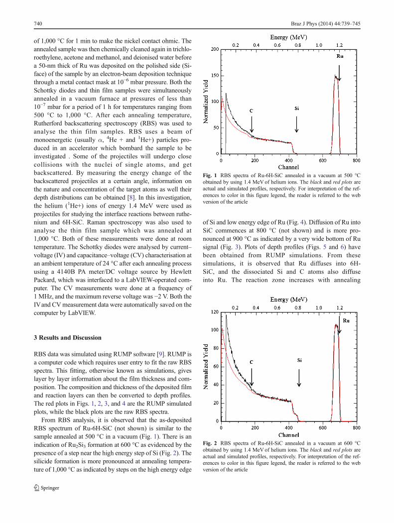
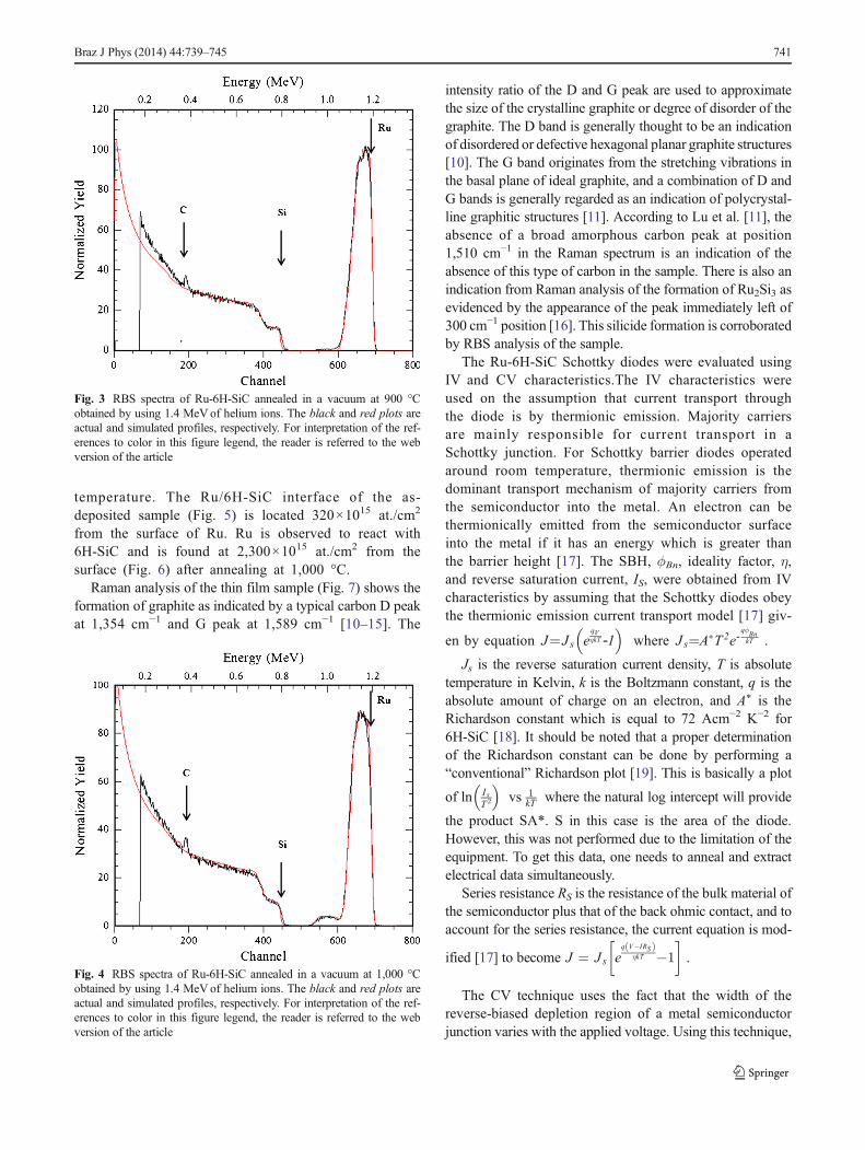
RBS data was simulated using RUMP software [9]. RUMP isa computer code which requires user entry to fit the raw RBSspectra. This fitting, otherwise known as simulations, giveslayer by layer information about the film thickness and com-position. The composition and thickness of the deposited filmand reaction layers can then be converted to depth profiles.The red plots in Figs. 1, 2, 3, and 4 are the RUMP simulatedplots, while the black plots are the raw RBS spectra.
From RBS analysis, it is observed that the as-depositedRBS spectrum of Ru-6H-SiC (not shown) is similar to thesample annealed at 500 °C in a vacuum (Fig. 1). There is anindication of Ru2Si3 formation at 600 °C as evidenced by thepresence of a step near the high energy step of Si (Fig. 2). Thesilicide formation is more pronounced at annealing tempera-ture of 1,000 °C as indicated by steps on the high energy edge
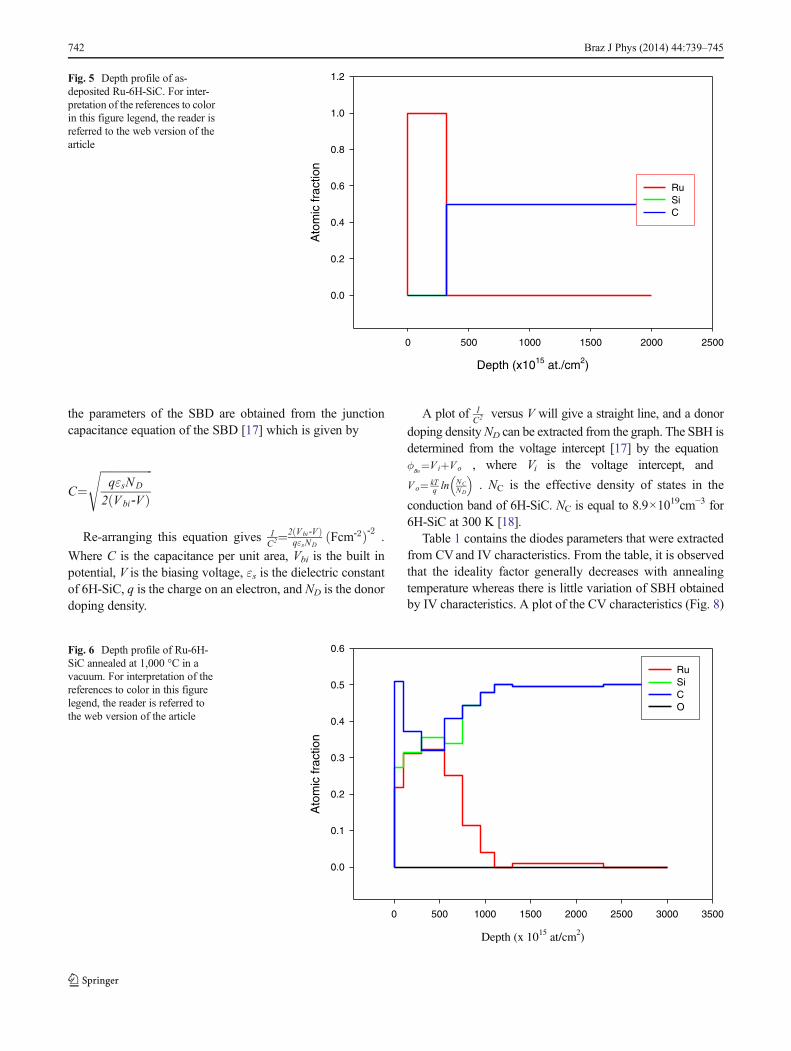
of Si and low energy edge of Ru (Fig. 4). Diffusion of Ru intoSiC commences at 800 °C (not shown) and is more pro-nounced at 900 °C as indicated by a very wide bottom of Rusignal (Fig. 3). Plots of depth profiles (Figs. 5 and 6) havebeen obtained from RUMP simulations. From thesesimulations, it is observed that Ru diffuses into 6H-SiC, and the dissociated Si and C atoms also diffuseinto Ru. The reaction zone increases with annealing
Fig. 1 RBS spectra of Ru-6H-SiC annealed in a vacuum at 500 °Cobtained by using 1.4 MeVof helium ions. The black and red plots areactual and simulated profiles, respectively. For interpretation of the ref-erences to color in this figure legend, the reader is referred to the webversion of the article
Fig. 2 RBS spectra of Ru-6H-SiC annealed in a vacuum at 600 °Cobtained by using 1.4 MeVof helium ions. The black and red plots areactual and simulated profiles, respectively. For interpretation of the ref-erences to color in this figure legend, the reader is referred to the webversion of the article
740 Braz J Phys (2014) 44:739–745
temperature. The Ru/6H-SiC interface of the as-deposited sample (Fig. 5) is located 320×1015 at./cm2
from the surface of Ru. Ru is observed to react with6H-SiC and is found at 2,300×1015 at./cm2 from thesurface (Fig. 6) after annealing at 1,000 °C.
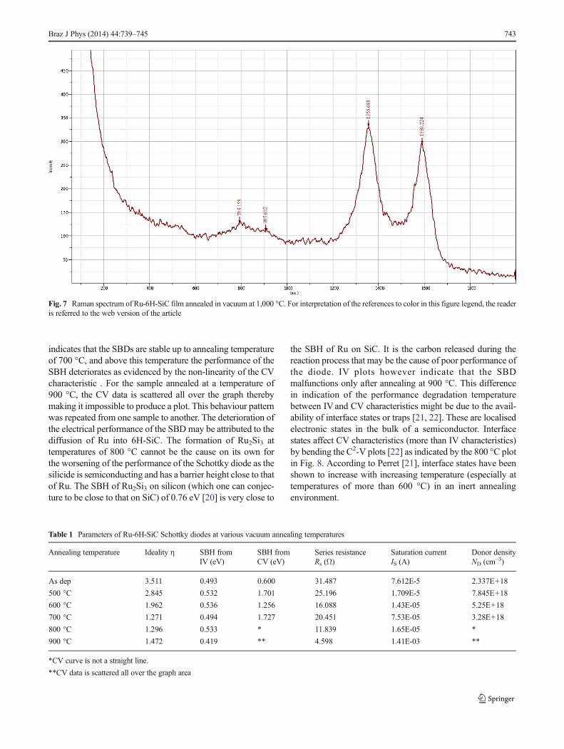
Raman analysis of the thin film sample (Fig. 7) shows theformation of graphite as indicated by a typical carbon D peakat 1,354 cm−1 and G peak at 1,589 cm−1 [10–15]. The
intensity ratio of the D and G peak are used to approximatethe size of the crystalline graphite or degree of disorder of thegraphite. The D band is generally thought to be an indicationof disordered or defective hexagonal planar graphite structures[10]. The G band originates from the stretching vibrations inthe basal plane of ideal graphite, and a combination of D andG bands is generally regarded as an indication of polycrystal-line graphitic structures [11]. According to Lu et al. [11], theabsence of a broad amorphous carbon peak at position1,510 cm−1 in the Raman spectrum is an indication of theabsence of this type of carbon in the sample. There is also anindication from Raman analysis of the formation of Ru2Si3 asevidenced by the appearance of the peak immediately left of300 cm−1 position [16]. This silicide formation is corroboratedby RBS analysis of the sample.
The Ru-6H-SiC Schottky diodes were evaluated usingIV and CV characteristics.The IV characteristics wereused on the assumption that current transport throughthe diode is by thermionic emission. Majority carriersare mainly responsible for current transport in aSchottky junction. For Schottky barrier diodes operatedaround room temperature, thermionic emission is thedominant transport mechanism of majority carriers fromthe semiconductor into the metal. An electron can bethermionically emitted from the semiconductor surfaceinto the metal if it has an energy which is greater thanthe barrier height [17]. The SBH, ϕBn, ideality factor, η,and reverse saturation current, IS, were obtained from IVcharacteristics by assuming that the Schottky diodes obeythe thermionic emission current transport model [17] giv-
en by equation J¼J s eqVηkT ‐1
� �where J s¼A�T2e‐
qϕBnkT .
Js is the reverse saturation current density, T is absolutetemperature in Kelvin, k is the Boltzmann constant, q is theabsolute amount of charge on an electron, and A∗ is theRichardson constant which is equal to 72 Acm−2 K−2 for6H-SiC [18]. It should be noted that a proper determinationof the Richardson constant can be done by performing a“conventional” Richardson plot [19]. This is basically a plot
of ln I sT2
� �vs 1
kT where the natural log intercept will provide
the product SA*. S in this case is the area of the diode.However, this was not performed due to the limitation of theequipment. To get this data, one needs to anneal and extractelectrical data simultaneously.
Series resistance RS is the resistance of the bulk material ofthe semiconductor plus that of the back ohmic contact, and toaccount for the series resistance, the current equation is mod-
ified [17] to become J ¼ J s eq V�IRSð Þ
ηkT �1
� �.
The CV technique uses the fact that the width of thereverse-biased depletion region of a metal semiconductorjunction varies with the applied voltage. Using this technique,
Fig. 3 RBS spectra of Ru-6H-SiC annealed in a vacuum at 900 °Cobtained by using 1.4 MeVof helium ions. The black and red plots areactual and simulated profiles, respectively. For interpretation of the ref-erences to color in this figure legend, the reader is referred to the webversion of the article
Fig. 4 RBS spectra of Ru-6H-SiC annealed in a vacuum at 1,000 °Cobtained by using 1.4 MeVof helium ions. The black and red plots areactual and simulated profiles, respectively. For interpretation of the ref-erences to color in this figure legend, the reader is referred to the webversion of the article
Braz J Phys (2014) 44:739–745 741
the parameters of the SBD are obtained from the junctioncapacitance equation of the SBD [17] which is given by
C¼ffiffiffiffiffiffiffiffiffiffiffiffiffiffiffiffiffiffiffiqεsND
2 Vbi‐Vð Þ
s
Re-arranging this equation gives 1C2¼2 Vbi‐Vð Þ
qεsNDFcm‐2ð Þ‐2 .
Where C is the capacitance per unit area, Vbi is the built inpotential, V is the biasing voltage, εs is the dielectric constantof 6H-SiC, q is the charge on an electron, and ND is the donordoping density.
A plot of 1C2 versus V will give a straight line, and a donor
doping densityND can be extracted from the graph. The SBH isdetermined from the voltage intercept [17] by the equationϕ
Bn¼V iþVo , where Vi is the voltage intercept, and
Vo¼ kTq ln
NCND
� �. NC is the effective density of states in the
conduction band of 6H-SiC. NC is equal to 8.9×1019cm−3 for6H-SiC at 300 K [18].
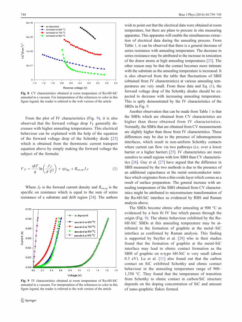
Table 1 contains the diodes parameters that were extractedfrom CVand IV characteristics. From the table, it is observedthat the ideality factor generally decreases with annealingtemperature whereas there is little variation of SBH obtainedby IV characteristics. A plot of the CV characteristics (Fig. 8)
Depth (x1015 at./cm2)
0 500 1000 1500 2000 2500
Ato
mic
frac
tion
0.0
0.2
0.4
0.6
0.8
1.0
1.2
Ru Si C
Fig. 5 Depth profile of as-deposited Ru-6H-SiC. For inter-pretation of the references to colorin this figure legend, the reader isreferred to the web version of thearticle
Depth (x 1015 at/cm2)
0 500 1000 1500 2000 2500 3000 3500
Ato
mic
frac
tion
0.0
0.1
0.2
0.3
0.4
0.5
0.6
Ru Si C O
Fig. 6 Depth profile of Ru-6H-SiC annealed at 1,000 °C in avacuum. For interpretation of thereferences to color in this figurelegend, the reader is referred tothe web version of the article
742 Braz J Phys (2014) 44:739–745
indicates that the SBDs are stable up to annealing temperatureof 700 °C, and above this temperature the performance of theSBH deteriorates as evidenced by the non-linearity of the CVcharacteristic . For the sample annealed at a temperature of900 °C, the CV data is scattered all over the graph therebymaking it impossible to produce a plot. This behaviour patternwas repeated from one sample to another. The deterioration ofthe electrical performance of the SBD may be attributed to thediffusion of Ru into 6H-SiC. The formation of Ru2Si3 attemperatures of 800 °C cannot be the cause on its own forthe worsening of the performance of the Schottky diode as thesilicide is semiconducting and has a barrier height close to thatof Ru. The SBH of Ru2Si3 on silicon (which one can conjec-ture to be close to that on SiC) of 0.76 eV [20] is very close to
the SBH of Ru on SiC. It is the carbon released during thereaction process that may be the cause of poor performance ofthe diode. IV plots however indicate that the SBDmalfunctions only after annealing at 900 °C. This differencein indication of the performance degradation temperaturebetween IVand CV characteristics might be due to the avail-ability of interface states or traps [21, 22]. These are localisedelectronic states in the bulk of a semiconductor. Interfacestates affect CV characteristics (more than IV characteristics)by bending the C2-V plots [22] as indicated by the 800 °C plotin Fig. 8. According to Perret [21], interface states have beenshown to increase with increasing temperature (especially attemperatures of more than 600 °C) in an inert annealingenvironment.
Fig. 7 Raman spectrum of Ru-6H-SiC film annealed in vacuum at 1,000 °C. For interpretation of the references to color in this figure legend, the readeris referred to the web version of the article
Table 1 Parameters of Ru-6H-SiC Schottky diodes at various vacuum annealing temperatures
Annealing temperature Ideality η SBH fromIV (eV)
SBH fromCV (eV)
Series resistanceRs (Ω)
Saturation currentIS (A)
Donor densityND (cm−3)
As dep 3.511 0.493 0.600 31.487 7.612E-5 2.337E+18
500 °C 2.845 0.532 1.701 25.196 1.709E-5 7.845E+18
600 °C 1.962 0.536 1.256 16.088 1.43E-05 5.25E+18
700 °C 1.271 0.494 1.727 20.451 7.53E-05 3.28E+18
800 °C 1.296 0.533 * 11.839 1.65E-05 *
900 °C 1.472 0.419 ** 4.598 1.41E-03 **
*CV curve is not a straight line.
**CV data is scattered all over the graph area
Braz J Phys (2014) 44:739–745 743
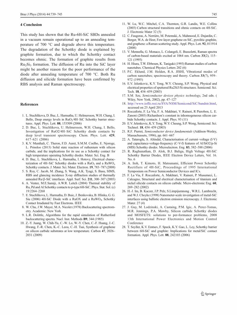
From the plot of IV characteristics (Fig. 9), it is alsoobserved that the forward voltage drop VF generally de-creases with higher annealing temperatures. This electricalbehaviour can be explained with the help of the equationof the forward voltage drop of the Schottky diode [23]which is obtained from the thermionic current transportequation above by simply making the forward voltage thesubject of the formula:
V F ¼ ηkT
qln
J F
A�T 2
� �þ ηϕBn þ Ron;sp J F ð1Þ
Where JF is the forward current density and Ron,sp is thespecific on resistance which is equal to the sum of seriesresistance of a substrate and drift region [24]. The authors
wish to point out that the electrical data were obtained at roomtemperature, but there are plans to procure in situ measuringapparatus. This apparatus will enable the simultaneous extrac-tion of electrical data during the annealing process. FromTable 1, it can be observed that there is a general decrease ofseries resistance with annealing temperature. The decrease inseries resistance may be attributed to the increase in ionizationof the donor atoms at high annealing temperatures [23]. Theother reason may be that the contact becomes more intimatewith the substrate as the annealing temperature is increased. Itis also observed from the table that fluctuations of SBH(obtained from IV characteristics) at various annealing tem-peratures are very small. From these data and Eq. (1), theforward voltage drop of the Schottky diodes should be ex-pected to decrease with increasing annealing temperature.This is aptly demonstrated by the IV characteristics of theSBDs in Fig. 9.
Another observation that can be made from Table 1 is thatthe SBHs which are obtained from CV characteristics arehigher than those obtained from IV characteristics.Normally, the SBHs that are obtained from CVmeasurementsare slightly higher than those from IV characteristics. Thesedifferences may be due to the presence of inhomogeneousinterfaces, which result in non-uniform Schottky contactswhere current can flow via two pathways (i.e. over a lowerbarrier or a higher barrier) [25]. IV characteristics are moresensitive to small regions with low SBH than CV characteris-tics [26]. Guy et al. [27] have argued that the difference inSBH measured by the two methods is due to the presence ofan additional capacitance at the metal–semiconductor inter-face which originates from a thin oxide layer which comes as aresult of surface preparation. The general increase with an-nealing temperature of the SBH obtained from CV character-istics might be attributed to microstructure transformation ofthe Ru-6H-SiC interface as evidenced by RBS and Ramananalysis above.
The SBDs become ohmic after annealing at 900 °C asevidenced by a best fit IV line which passes through theorigin (Fig. 9). The ohmic behaviour exhibited by the Ru-6H-SiC SBDs at this annealing temperature may be at-tributed to the formation of graphite at the metal–SiCinterface as confirmed by Raman analysis. This findingis supported by Seyller et al. [28] who in their studiesfound that the formation of graphite at the metal-SiCinterface may lead to ohmic contact formation as theSBH of graphite on n-type 6H-SiC is very small (about0.3 eV). Lu et al. [11] also found out that the carboncontact on SiC exhibited Schottky and ohmic contactbehaviour in the annealing temperature range of 900–1,350 °C. They found that the temperature of transitionfrom Schottky to ohmic contact in carbon/SiC structuredepends on the doping concentration of SiC and amountof nano-graphitic flakes formed.
Reverse voltage (V)
-1.4 -1.2 -1.0 -0.8 -0.6 -0.4 -0.2 0.0 0.2 0.4
1/C
2 (Fcm
-2)-2
0
5e+17
1e+18
2e+18
2e+18
as-depositedannealed at 600 oCannealed at 700 oCannealed at 800 oC
Fig. 8 CV characteristics obtained at room temperature of Ru-6H-SiCannealed in a vacuum. For interpretation of the references to color in thisfigure legend, the reader is referred to the web version of the article
Fig. 9 IV characteristics obtained at room temperature of Ru-6H-SiCannealed in a vacuum. For interpretation of the references to color in thisfigure legend, the reader is referred to the web version of the article
744 Braz J Phys (2014) 44:739–745
4 Conclusion
This study has shown that the Ru-6H-SiC SBDs annealedin a vacuum remain operational up to an annealing tem-perature of 700 °C and degrade above this temperature.The degradation of the Schottky diode is explained bygraphite formation, due to which the Schottky contactbecomes ohmic. The formation of graphite results fromRu2Si3 formation. The diffusion of Ru into the SiC layermight be another reason for the poor performance of thediode after annealing temperature of 700 °C. Both Rudiffusion and silicide formation have been confirmed byRBS analysis and Raman spectroscopy.
References
1. L. Stuchlikova, D. Buc, L. Harmatha, U. Helmersson,W.H. Chang, I.Bello, Deep energy levels in RuO2/4H–SiC Schottky barrier struc-tures. Appl. Phys. Lett. 88, 153509 (2006)
2. D. Buc, L. Stuchlikova, U. Helmersson, W.H. Chang, I. Bello,Investigation of RuO2/4H–SiC Schottky diode contacts bydeep level transient spectroscopy. Chem. Phys. Lett. 429,617–621 (2006)
3. K.V. Munthali, C. Theron, F.D. Auret, S.M.M. Coelho, E. Njoroge,L. Prinsloo (2013) Solid state reaction of ruthenium with siliconcarbide, and the implications for its use as a Schottky contact forhigh temperature operating Schottky diodes. Mater. Sci. Eng. B
4. D. Buc, L. Stuchlikova, L. Harmatha, I. Hotovy, Electrical charac-terization of 4H–SiC Schottky diodes with a RuO2 and a RuWOx
Schottky contacts. J. Mater. Sci. Mater. Electron. 19, 783–787 (2008)5. S. Roy, C. Jacob, M. Zhang, S. Wang, A.K. Tyagi, S. Basu, SIMS,
RBS and glancing incidence X-ray diffraction studies of thermallyannealed Ru/β-SiC interfaces. Appl. Surf. Sci. 211, 300–307 (2003)
6. A. Venter, M.E.Samiji, A.W.R. Leitch (2004) Thermal stability ofRu, Pd andAl Schottky contacts to p-type 6H-SiC. Phys. Stat. Sol. (c)19:2264–2268
7. E. Stuchlikova, L. Harmatha, D. Buic, J. Benkovska, B. Hlinka, G. G.Siu (2006) 4H-SiC Diode with a RuOX and a RuWOX SchottkyContact Irradiated by Fast Electrons. IEEE
8. W. Chu, J.W. Mayer, M.A. Nicolet (1978) Backscattering spectrom-etry. Academic: New York
9. L.R. Dolittle, Algorithms for the rapid simulation of Rutherfordbackscattering spectra. Nucl. Inst. Methods B9, 344 (1985)
10. Z.-Y. Juang, W. Chih-Yu, C.-W. Lo, W.-Y. Chen, C.-F. Huang, J.-C.Hwang, F.-R. Chen, K.-C. Leou, C.-H. Tsai, Synthesis of grapheneon silicon carbide substrates at low temperature. Carbon 47, 2026–2031 (2009)
11. W. Lu, W.C. Mitchel, C.A. Thornton, G.R. Landis, W.E. Collins(2003) Carbon structural transitions and ohmic contacts on 4H-SiC.J. Electronic Mater 32 (5)
12. C. Faugeras, A. Nerrière, M. Potemski, A.Mahmood, E. Dujardin, C.Berger, W.A. de Heer, Few-layer graphene on SiC, pyrolitic graphite,and graphene: a Raman scattering study. Appl. Phys. Lett. 92, 011914(2008)
13. V. Mennella, G. Monaco, L. Colangeli, E. Bussoletti, Raman spectraof carbon-based materials excited at 1064 nm. Carbon 33(2), 115–121 (1995)
14. H. Hiura, T.W. Ebbesen, K. Tanigaki (1993) Raman studies of carbonnanotubes. Chemical Physics Letters 202 (6)
15. P.C. Eklund, J.M. Holden, R.A. JISHI, Vibrational modes ofcarbon nanotubes; spectroscopy and theory. Carbon 33(7), 959–972 (1995)
16. E.V. Jelenkovic, K.Y. Tong, W.Y. Cheung, S.P. Wong, Physical andelectrical properties of sputtered Ru2Si3/Si structures. Semicond. Sci.Tech. 18, 454–459 (2003)
17. S.M. Sze, Semiconductor devices physics technology, 2nd edn. (Wiley, New York, 2002), pp. 47–127
18. http://www.ioffe.rssi.ru/SVA/NSM/Semicond/SiC/bandstr.html,accessed on 25 April 2013
19. Roccaforte, F. La Via, F. A. Makhtari, V. Raineri, R Pierobon, L. E.Zanoni (2003) Richardson’s constant in inhomogeneous silicon car-bide Schottky contacts. J. Appl. Phys. 93 (11)
20. E.V. Jelenkovic, K.Y. Tong,W.Y. Cheung, S.P.Wong, Semicond. Sci.Technol. 18, 454–459 (2003)
21. R.F. Pierret, Semiconductor device fundamentals (Addison-Wesley,Massachussets, 1996), pp. 661–667
22. A. Tataroglu, S. Altindal, Characterisation of current–voltage (I-V)and capacitance-voltage-frequency (C-V-f) features of Al/SiO2/p-Si(MIS) Schottky diodes. Microelectron. Eng. 83, 582–588 (2006)
23. R. Raghunathan, D. Alok, B.J. Baliga, High Voltage 4H-SiCSchottky Barrier Diodes, IEEE Electron Device Letters, Vol. 16.No. 6
24. A. Itoh, T. Kimoto, H. Matsunami, Efficient Power SchottkyRectifiers of 4H-SiC, Proceedings of 1995 InternationalSymposium on Power Semiconductor Devices and ICs.
25. F. La Via, F. Roccaforte, A. Makhtari, V. Raineri, P. Musumeci, L.Calcagno, Structural and electrical characterisation of titanium andnickel silicide contacts on silicon carbide. Micro-electronic Eng. 60,269–282 (2002)
26. H.-J. Im, B. Kaczer, J.P. Pelz, S.Limpijumnong , W.R.L. Lambrecht,and W.J. Choyke (1998) Nanometer-scale investigation of metal-SiCinterfaces using ballistic electron emission microscopy. J. ElectronicMater. 27 (4)
27. J. Guy, M. Lodzinski, A. Castaing, P.M. Igic, A. Perez-Tomas,M.R. Jennings, P.A. Mawby, Silicon carbide Schottky diodesand MOSFETS: solutions to per-formance problems, 200813th International Power Electronics and Motion ControlConference
28. T. Seyller, K.V. Emtsev, F. Speck, K.Y. Gao, L. Ley, Schottky barrierbetween 6H-SiC and graphite: Implications for metal/SiC contactformation. Appl. Phys. Lett. 88, 242103 (2006)
Braz J Phys (2014) 44:739–745 745


![Grammatical notes and vocabulary of Nagnuma primier [sic]](https://static.fdokumen.com/doc/165x107/6324da70e491bcb36c0a0414/grammatical-notes-and-vocabulary-of-nagnuma-primier-sic.jpg)