ONLINE JUNCTION TEMPERATURE ESTIMATION OF SIC ...
183
ONLINE JUNCTION TEMPERATURE ESTIMATION OF SIC POWER MOSFETS Xiang Lu B.Eng, MSc. A thesis submitted for the degree of Doctor of Philosophy November 2019 School of Engineering Newcastle University United Kingdom
-
Upload
khangminh22 -
Category
Documents
-
view
2 -
download
0
Transcript of ONLINE JUNCTION TEMPERATURE ESTIMATION OF SIC ...

ONLINE JUNCTION TEMPERATURE
ESTIMATION OF SIC POWER MOSFETS
Xiang Lu
B.Eng, MSc.
A thesis submitted for the degree of
Doctor of Philosophy
November 2019
School of Engineering
Newcastle University
United Kingdom


Acknowledgement
I
Acknowledgement
I would like to firstly show my gratitude to my supervisors, Professor Volker Pickert, Dr Maher
Al-Greer and Dr Charalampos Tsimenidis, for their valuable guidance and constant support. I
also need to express my thanks to Dr Bing Ji for his priceless suggestions on my work. This
research work would not be successfully completed without their support.
My gratitude is also to the school of Electrical and Electronic Engineering, especially to the
staff at the Power Electronics, Drives and Machines group for providing the suitable working
and experimental environment for my research work. I also want to thank other PhD student in
Power Electronics, Drives and Machines group for their inspirations appeared during academic
discussions. My thanks go to Mr. James Richardson, Mr. Gordon Marshall and other technical
support staff at UG lab and staff from the Mechanical workshop as well as Electronic workshop
for their technical assistance during this research work. My special thanks go to Postgraduate
Research Coordinator, Mrs. Gillian Webber and her co-workers for their help.
Dr Haimeng Wu deserves the acknowledgement for his wise advices on my research work and
the help provided when I encountered difficulties during the research.
I would also like to thank Dr Huaxia Zhan for her accompany for the past four years.
Finally, I would like to say thank you to my parents for their unconditional support and
encouragement. There is nothing can be compatible with their love for me.
Abstract
II
Abstract
Silicon Carbide (SiC) based power devices receive more and more popularity in the field of
power electronics as they operate at higher voltages, higher switching frequencies and higher
temperatures compared to traditional Silicon (Si) based power modules. As for SiC-based
power devices, the temperature of SiC chip must be monitored in order to operate the device
within its limit.
However, it is not straight forward to directly measure the junction temperature (Tj) of a power
device non-intrusively due to the package obstruction. Therefore, indirect Tj measurement
methods like Temperature Sensitive Electrical Parameters (TSEPs) are preferred by researchers
and been intensively investigated for Si devices as the dominant power devices in the past.
However, those TSEPs which are effective for Si devices are mostly not applicable to SiC
devices. This is due to different physical and electrical behaviour between SiC-based device
and Si-based device. Thus, it is necessary to develop new method to implement indirect Tj
measurement for SiC devices.
This thesis presents a new on-line technique to estimate the Tj of discrete SiC MOSFET devices.
In this work, small amplitude, high frequency chirp signals are injected into the gate of a
discrete SiC device during its off-state operation. Then, the gate-source voltage (VGS) is
measured and its frequency response (FR) characteristic is determined by using Discrete Fast
Fourier Transform (DFFT) analysis. The captured VGS signal is a direct function of the gate-
source loop impedance. The derived function becomes a linear function in respect Tj as it
represents only the resistive elements of the gate-source loop. As the gate channel resistance of
the SiC MOSFET (Rint) is the largest resistance in that loop and it is temperature dependent. As
a result, the temperature of the SiC MOSFET chip can be estimated.
The new method in the thesis will be explained in details and the theory will be backed up by
analytical simulations. A 3D numerical model for the discrete SiC MOSFET is also established
and simulated. Furthermore, a network analyser is used for initial validation of the new method
and finally a boost circuit was built with signal injection circuit integrated within the gate driver
circuit to demonstrate the feasibility of using this innovative method to extract junction
temperature of a discrete SiC MOSFET.
Keywords- SiC MOSFET, Junction Temperature, Small AC Signal Injection

Table of Contents
IV
Table of Contents Acknowledgement .................................................................................................................. I
Abstract ................................................................................................................................ II
List of Figures ...................................................................................................................... VI
List of Tables .................................................................................................................... XIII
List of Abbreviations ........................................................................................................ XIV
Chapter 1 Introduction ........................................................................................................... 1
1.1 Background ........................................................................................................... 1
1.2 Wideband-gap semiconductor ............................................................................... 3
1.3 Objectives ............................................................................................................. 4
1.4 Contribution to knowledge .................................................................................... 4
1.5 Thesis outline ........................................................................................................ 5
Chapter 2 Overview of SiC MOSFET and State-of-Art Tj Measurement Techniques .............. 8
2.1 Comparison of physical structure and characteristics of Si and SiC MOSFET ....... 8
2.2 Comparison of switching characteristics of Si and SiC MOSFETs....................... 12
2.3 Direct temperature measurement techniques ........................................................ 13
2.4 Indirect temperature measurement techniques ..................................................... 18
2.4.1 Component-on-die Tj extraction ....................................................................... 19
2.4.2 Measurement of Tj during device on-state ........................................................ 20
2.4.3 Tj measurement during device switching transient............................................ 24
2.4.4 Thermal model based Tj acquisition ................................................................. 31
2.5 Conclusion .......................................................................................................... 33
Chapter 3 3D Thermal Model Establishment and FEM Thermal Simulation ......................... 35
3.1 Establishing 3D Thermal Model .......................................................................... 35
3.2 3D Model Internal Power Loss Calculation ......................................................... 39
3.3 Finite Element Analysis of the 3D SiC MOSFET Model ..................................... 46
3.4 Conclusion .......................................................................................................... 51

Table of Contents
V
Chapter 4: Small signal modelling of SiC MOSFETs ........................................................... 52
4.1 TSEP simulation in the SiC MOSFET ................................................................. 52
4.2 Introduction of small signal AC analysis in power electronics ............................. 56
4.3 Small AC signal modelling of the SiC MOSFET ................................................. 57
4.4 Off-state small AC signal equivalent circuit modelling of the SiC MOSFET ....... 59
4.5 Parametric calculation of individual parasitic for MOSFET ................................. 60
4.5.1 Nominal values calculation of parasitic of SiC MOSFET ................................. 60
4.5.2 Parasitic parameters of SiC MOSFET when considering temperature influence. 63
4.6 Verification of small ac signal equivalent circuit ................................................. 64
4.7 Conclusion .......................................................................................................... 76
Chapter 5. Experimental Implementation Based on Small AC Signal Injection Technique ... 77
5.1 Gate source voltage dependency against temperature .......................................... 77
5.1.1 Unbiased test ................................................................................................... 77
5.1.2 Biased test with chirp signal injection .............................................................. 83
5.2 Conclusion ........................................................................................................ 112
Chapter 6 Conclusion and future work ............................................................................... 113
Appendix A: State-of-art of TSEPs .................................................................................... 115
A.1 Introduction ...................................................................................................... 115
A.2 Steady-state TSEPs ........................................................................................... 115
A.3 Dynamic TSEPs ................................................................................................ 118
A.4 Other TSEPs ..................................................................................................... 129
A.1 Conclusion ........................................................................................................ 131
Appendix B: State-of-art Gate Driver Topologies ............................................................... 132
B.1 Comparison of Si and SiC MOSFET gate drivers .............................................. 132
B.2 Conclusion ........................................................................................................ 141
Appendix C: Unbiased Test ............................................................................................... 143

Table of Contents
VI
Appendix D: Schematic of 4-leg Inverter ........................................................................... 144
Appendix E: SiC MOSFET Gate Driver Pictures ............................................................... 145
Appendix F: Pico-scope Spectrum Mode ............................................................................ 148
F.1 Basic controls of Pico-scope spectrum mode ..................................................... 148
F.2 Spectrum options............................................................................................... 149
F.2.1 Spectrum bins ................................................................................................ 149
F.2.2 Window function ........................................................................................... 150
F.2.3 Display mode ................................................................................................. 151
F.2.4 Scales ............................................................................................................ 153
F.3 Conclusion ........................................................................................................ 154
Reference ........................................................................................................................... 155

List of Figures
VI
List of Figures
Figure 1. 1 Industrial survey of fragile components in power electronic converters [2]. .......... 1
Figure 1. 2 An example of Tj profile of a power electronic device. ......................................... 2
Figure 2. 1 Comparison of Si, SiC, and GaN material characteristics [17]. ............................. 9
Figure 2. 2 Comparison of on-state resistance versus temperature of Cool MOSFET and SiC
MOSFET at various gate voltages [28]. ................................................................................ 12
Figure 2. 3 Test bench for IR measurements [32]. ................................................................ 14
Figure 2. 4 An IGBT module with embedded NTC sensor [40]. ........................................... 15
Figure 2. 5 IGBT module with on-die temperature sensing diodes [46]. ............................... 16
Figure 2. 6 Parasitic capacitances between the sensing diode and power device [46]. ........... 17
Figure 2. 7 Principal circuit for IGBT Tj sensing based on diode forward voltage. ................ 17
Figure 2. 8 Principal circuit for internal gate resistor measurement. ...................................... 20
Figure 2. 9 Principal circuit for sensing base-emitter voltage for BJT. .................................. 21
Figure 2. 10 Principal circuit for sensing the on-state resistor for MOSFET. ........................ 21
Figure 2. 11 Principal circuit for sensing on on-state voltage for IGBT................................. 22
Figure 2. 12 Principal circuit for the detection of Miller plateau width during turn-off transient.
............................................................................................................................................ 24
Figure 2. 13 Principal circuit to measure VeE delay time. ...................................................... 25
Figure 2. 14 Principal Tj measurement of the voltage switching times. ................................. 26
Figure 2. 15 Principal circuit for short-circuit Tj measurement. ............................................. 27
Figure 2. 16 Principal circuit for IGBT VeE peak measurement. ............................................ 28
Figure 2. 17 Principle circuit for MOSFET VTH measurement. .............................................. 29
Figure 2. 18 Principle circuit of integration of VGE measurement. ......................................... 29
Figure 2. 19 Principle circuit for MOSFET IGPeak measurement. ........................................... 30
Figure 2. 20 Principle circuit for IGBT IGE integration measurement. ................................... 30
Figure 2. 21 Tj estimation based on an open-loop observer. .................................................. 32
Figure 2. 22 Tj estimation based on a closed-loop observer. .................................................. 32
Figure 3. 1 TO247-3 Package outer dimension. .................................................................... 36
Figure 3. 2 C2M0080120D bare die dimension graph. .......................................................... 37
Figure 3. 3 3D thermal model of C2M0080120D SiC MOSFET with heat plate: (a) complete
package model, (b) internal view with top capsule removed, (c) bare die model. .................. 39
Figure 3. 4 On-Resistance VS. Temperature for different gate source voltages. .................... 40
Figure 3. 5 Typical boost converter topology used for MOSFET power loss calculation. ...... 41
Figure 3. 6 Forward characteristics of Cree/Wolfspeed C4D20120D SiC Schottky diode. .... 42

List of Figures
VII
Figure 3. 7 Typical characteristics of power MOSFET switching transients. ........................ 44
Figure 3. 8 Temperature distribution of SiC MOSFET sitting on voltage-controlled heat plate
(25°C): (a). SiC die body temperature distribution; (b). SiC die body back temperature
distribution; (c). Chip and heat plate temperature distribution when the top package is hided.
............................................................................................................................................ 46
Figure 3. 9 Temperature distribution of SiC MOSFET sitting on voltage-controlled heat plate
(50°C): (a). SiC die body temperature distribution; (b). SiC die body back temperature
distribution; (c). Chip and heat plate temperature distribution when the top package is hided.
............................................................................................................................................ 48
Figure 3. 10 Temperature distribution of SiC MOSFET sitting on voltage-controlled heat plate
(75°C): (a). SiC die body temperature distribution; (b). SiC die body back temperature
distribution; (c). Chip and heat plate temperature distribution when the top package is hided.
............................................................................................................................................ 49
Figure 3. 11 Temperature distribution of SiC MOSFET sitting on voltage-controlled heat plate
(100°C): (a). SiC die body temperature distribution; (b). SiC die body back temperature
distribution; (c). Chip and heat plate temperature distribution when the top package is hided.
............................................................................................................................................ 50
Figure 3. 12 Temperature distribution of SiC MOSFET sitting on voltage-controlled heat plate
(125°C): (a). SiC die body temperature distribution; (b). SiC die body back temperature
distribution; (c). Chip and heat plate temperature distribution when the top package is hided.
............................................................................................................................................ 51
Figure 3. 1 TO247-3 Package outer dimension. .................................................................... 36
Figure 3. 2 C2M0080120D bare die dimension graph........................................................... 37
Figure 3. 3 3D thermal model of C2M0080120D SiC MOSFET with heat plate: (a) complete
package model, (b) internal view with top capsule removed, (c) bare die model. .................. 39
Figure 3. 4 On-Resistance VS. Temperature for different gate source voltages. .................... 40
Figure 3. 5 Typical boost converter topology used for MOSFET power loss calculation....... 41
Figure 3. 6 Forward characteristics of Cree/Wolfspeed C4D20120D SiC Schottky diode. .... 42
Figure 3. 7 Typical characteristics of power MOSFET switching transients. ........................ 44
Figure 3. 8 Temperature distribution of SiC MOSFET sitting on voltage-controlled heat plate
(25°C): (a). SiC die body temperature distribution; (b). SiC die body back temperature
distribution; (c). Chip and heat plate temperature distribution when the top package is hided.
............................................................................................................................................ 46
Figure 3. 9 Temperature distribution of SiC MOSFET sitting on voltage-controlled heat plate
(50°C): (a). SiC die body temperature distribution; (b). SiC die body back temperature

List of Figures
VIII
distribution; (c). Chip and heat plate temperature distribution when the top package is hided.
............................................................................................................................................ 48
Figure 3. 10 Temperature distribution of SiC MOSFET sitting on voltage-controlled heat plate
(75°C): (a). SiC die body temperature distribution; (b). SiC die body back temperature
distribution; (c). Chip and heat plate temperature distribution when the top package is hided.
............................................................................................................................................ 49
Figure 3. 11 Temperature distribution of SiC MOSFET sitting on voltage-controlled heat plate
(100°C): (a). SiC die body temperature distribution; (b). SiC die body back temperature
distribution; (c). Chip and heat plate temperature distribution when the top package is hided.
............................................................................................................................................ 50
Figure 3. 12 Temperature distribution of SiC MOSFET sitting on voltage-controlled heat plate
(125°C): (a). SiC die body temperature distribution; (b). SiC die body back temperature
distribution; (c). Chip and heat plate temperature distribution when the top package is hided.
............................................................................................................................................ 51
Figure 4. 1(a) Dependency of n-state resistance on temperature for different MOSFET
technologies; (b) silicon PiN diode reverse recovery characteristics at different temperatures;
(c) SiC Schottky diode turn-off characteristics at different temperatures; (d) silicon IGBT gate
voltage during turn-off at different temperatures; (e) SiC MOSET gate voltage during turn-off
at different temperatures [15]. .............................................................................................. 53
Figure 4. 2 DPT test based on Cree C2M0080120D discrete MOSFET. ............................... 54
Figure 4. 3 Simulation results of DPT tests, including VDS, VGS and ID. ................................ 55
Figure 4. 4 Typical switching loop of an inductive load circuit. ............................................ 58
Figure 4. 5 Off-state equivalent circuit of a SiC MOSFET. ................................................... 59
Figure 4. 6 Typical parasitic capacitance VS VDS for C2M0080120D [82]. ........................... 60
Figure 4. 7 Schematic of un-biased off-state gate-source equivalent circuit for SiC MOSFET.
............................................................................................................................................ 64
Figure 4. 8 Simulation results for gate-source loop impedance response at room temperature.
............................................................................................................................................ 65
Figure 4. 9 Experiment set-ups: (a) Agilent Keysight E5071B Network analyzer; ................ 66
Figure 4. 10 Simulation results and network analyser results: (a) impedance magnitude at
T=25oC; (b) impedance phase at T=25oC. ............................................................................ 66
Figure 4. 11 Off-state gate-source loop impedance frequency response at 5 different Tj. ....... 67
Figure 4. 12 Impedance VS Tj at 10 MHz. ............................................................................ 68
Figure 4. 13 LTspice Simulation Schematics: (a) Top switch is off and the small AC signal is
superimposed into the gate terminal of the SiC MOSFET while the bottom switch is at its on-

List of Figures
IX
stated; (b) Top switch is at its on-stated while the small AC signal is superimposed into the gate
terminal of bottom switch; (c) Small AC chirp signal is superimposed into the gate terminal of
a discrete SiC MOSFET when it is completely off. .............................................................. 70
Figure 4. 14 Frequency response comparison of three different simulation setups. ............... 71
Figure 4. 15 The frequency response of gate-source voltage of the top switch with small AC
signal injection when it is off while the bottom switch is on:(a) Full sweeping frequency range;
(b) Zoomed in frequency response at resonant frequency. .................................................... 73
Figure 4. 16 The frequency response of gate-source voltage of the bottom switch with small
AC signal injection when it is off while the bottom switch is on:(a) Full sweeping frequency
range; (b) Zoomed in frequency response at resonant frequency. .......................................... 74
Figure 4. 17 The frequency response of gate-source voltage of the single discrete SiC MOSFET
with small AC signal injection when it is off while the bottom switch is on:(a) Full sweeping
frequency range; (b) Zoomed in frequency response at resonant frequency. ......................... 75
Figure 5. 1 Small chirp signal injection into gate-source terminals of SiC MOSFET during off-
state under un-biased condition. ........................................................................................... 79
Figure 5. 2 Photograph of unbiased experimental test set-up. ............................................... 79
Figure 5. 3 Frequency response analysis: (a) Frequency response of magnitude of VGSpeak from
5 MHz to 10 MHz; (b) integrated magnitude of VGSpeak. ........................................................ 82
Figure 5. 4 Schematic of signal injection test under DC biased condition using a 4-leg inverter.
............................................................................................................................................ 83
Figure 5. 5 Photograph of the overall test rig set-up.............................................................. 84
Figure 5. 6 Biased tests: (a) test rig overview; (b) 4-leg inverter with SiC MOSFET in phase
leg on voltage-controlled heat plate. ..................................................................................... 85
Figure 5. 7 VGSPeak against f (from 7 MHz to 10 MHz) at different values of Tj under 50 V DC
biasing. ................................................................................................................................ 87
Figure 5. 8 Value of VGSPeaktotal between 7 MHz and 10 MHz under 50 V DC biasing against Tj.
............................................................................................................................................ 89
Figure 5. 9 VGSPeak against f (from 7 MHz to 10 MHz) at different Tj under 100 V DC biasing.
............................................................................................................................................ 90
Figure 5. 10 VGSPeaktotal between 7 MHz and 10 MHz under 100 V DC biasing against Tj. ..... 91
Figure 5. 11 VGSPeak against f (from 7 MHz to 10 MHz) at different Tj under 200 V DC biasing.
............................................................................................................................................ 91
Figure 5. 12 VGSPeaktotal between 7 MHz and 10 MHz under 200 V DC biasing against Tj. ..... 92
Figure 5. 13 VGSPeak against f (from 7 MHz to 10 MHz) at different Tj under 300 V DC biasing.
............................................................................................................................................ 92

List of Figures
X
Figure 5. 14 VGSPeaktotal between 7 MHz and 10 MHz under 300 V DC biasing against Tj. ..... 93
Figure 5. 15 VGSPeak against f (from 7 MHz and 10 MHz) at different Tj under 400 V DC biasing.
............................................................................................................................................ 94
Figure 5. 16 VGSPeaktotal between 7 MHz and 10 MHz under 400 V DC biasing against Tj. ..... 94
Figure 5. 17 VGSPeak against f (from 7 MHz to 10 MHz) at different Tj under 500 V DC biasing.
............................................................................................................................................ 95
Figure 5. 18 VGSPeaktotal between 7 MHz and 10 MHz under 500 V DC biasing against Tj. ..... 96
Figure 5. 19 VGSPeak against f (from 7 MHz to 10 MHz) at different Tj under 600 V DC biasing.
............................................................................................................................................ 96
Figure 5. 20 VGSPeaktotal between 7 MHz and 10 MHz under 600 V DC biasing against Tj. ..... 97
Figure 5. 21 Comparison of DC biasing conditions for small AC signal injection technique. 98
Figure 5. 22 Schematics for Cree CRD-001 gate driver for 2nd generation SiC MOSFET. .. 100
Figure 5. 23 Chirp signal input and output comparison at 5 MHz by using wide-band RF
transformer. ....................................................................................................................... 101
Figure 5. 24 Chirp signal input and output comparison at 7.4 MHz by using wide-band RF
transformer. ....................................................................................................................... 102
Figure 5. 25 Chirp signal input and output comparison at 9.3 MHz by using wide-band RF
transformer. ....................................................................................................................... 102
Figure 5. 26 VGSPeak against f at 300 V DC biasing with injection via gate driver with 5 V peak-
to-peak injection amplitude. ............................................................................................... 103
Figure 5. 27 VGSPeaktotal against Tj under 300 V DC biasing with injection via gate driver with
5 V peak-to-peak amplitude injection signal. ...................................................................... 104
Figure 5. 28 VGSPeak against f under 300 V DC biasing with injection via gate driver with 2 V
injection amplitude. ............................................................................................................ 104
Figure 5. 29 VGSPeaktotal against Tj under 300 V DC biasing with injection via gate driver with
2 V peak to peak amplitude injection signal. ....................................................................... 105
Figure A 1 Isat value as a function of Tj at different voltage conditions [94]. ....................... 116
Figure A 2 Comparison of collector leakage current under different VCE [95]. .................... 117
Figure A 3 VCE(on) of an IGBT as a function of Tj for different Im [91]. ............................... 118
Figure A 4 Transconductance of a 3 kV 1200 A IGBT Module [98]. .................................. 119
Figure A 5 Turn-on transient behaviour of VGE at different Tj [100] .................................... 120
Figure A 6 Change in IGBT VTH with increasing Tj [98]. .................................................... 120
Figure A 7 VTH as a function of Tj for different IC and VCE value [96] ................................. 121

List of Figures
XI
Figure A 8 VGE waveforms at different temperatures for an IGBT measured at a 600 V, 100 A
switching condition [101]. .................................................................................................. 122
Figure A 9 Time difference between the first falling edge and second falling edge of the Vge
waveform at the 600 V, 100 A switching condition [101]. .................................................. 122
Figure A 10 Typical turn-on process of IGBT [66]. ............................................................ 123
Figure A 11 td(on) as a function of Tj and ID [100]. ............................................................... 124
Figure A 12 td(on) as a function of Tj and VDC [100].............................................................. 124
Figure A 13 Typical turn-off process of IGBT [66]. ........................................................... 125
Figure A 14 Variation in td(off) with Tj and IL: (a)VDC=1400 V and (b) VDC=1600 V [66]. .... 126
Figure A 15 Variation of td(off) with Tj and VDC: (a)IL=1000 A and (b) IL=1200 A [66]. ....... 126
Figure A 16 Measured dVCE/dt values and linear fitted curves against Tj for varying IL at: (a)
VDC of 160 V; (b) VDC of 300 V [106]. ............................................................................... 127
Figure A 17 The Measured dIC/dt at two different gate voltages [107]. ............................... 128
Figure A 18 Turn-off waveform of a commercial IGBT at 150 ˚C, rated current (IRG7IC23FD)
[108][108][108](108). ........................................................................................................ 128
Figure A 19 Behavior of Itail at different Tj [99]. ................................................................. 129
Figure A 20 Energy dissipation at turning-on as a function of Tj [104]. .............................. 130
Figure B 1 Push-pull voltage source gate driver. ................................................................ 132
Figure B 2 Push-pull gate driver turn-on transient. ............................................................. 133
Figure B 3 Push-pull gate driver turn-off transient.............................................................. 133
Figure B 4 Current mirror gate driver. ................................................................................ 135
Figure B 5 Current mirror gate driver turn-on transient. ..................................................... 135
Figure B 6 Current mirror gate driver turn-off transient. ..................................................... 136
Figure B 7 Inductor-based current source gate driver.......................................................... 137
Figure B 8 Inductor-based gate driver turn-on transient: step 1. .......................................... 137
Figure B 9 Inductor-based gate driver turn-on transient: step 2. .......................................... 138
Figure B 10 Inductor-based gate driver turn-on transient: step 3. ........................................ 138
Figure B 11 Inductor-based gate driver turn-on transient: step 4. ........................................ 139
Figure B 12 Inductor-based gate driver turn-off transient: step 5. ....................................... 139
Figure B 13 Inductor-based gate driver turn-off transient: step 6. ....................................... 140
Figure B 14 Inductor-based gate driver turn-off transient: step 7. ....................................... 140
Figure B 15 Inductor-based gate driver turn-off transient: step 8. ....................................... 141
Figure C 1 Schematic of PCB board used for unbiased test. ............................................... 143
Figure D. 1 Schematic of 4-leg inverter. ............................................................................. 144
Figure E 1 Isolated gate driver: (a) top view; (b) bottom view [119]. ................................. 145

List of Figures
XII
Figure E 2 Isolated gate driver schematic [119]. ................................................................. 146
Figure E 3 Mechanical drawing of isolated gate driver [119]. ............................................ 147
Figure F 1 Spectrum example of a 700 kHz sinusoidal waveform. ..................................... 148
Figure F 2 Spectrum options are presented. ........................................................................ 149
Figure F 3 An example of spectrum bins. ........................................................................... 150
Figure F 4 Example of Magnitude view of spectrum mode in Pico-scope. .......................... 151
Figure F 5 Example of Average view of spectrum mode in Pico-scope. .............................. 152
Figure F 6 Example of Peak Hold view of spectrum mode in Pico-scope between 1 kHz and
100 kHz. ............................................................................................................................ 153
Figure F 7 X axis display modes: (a) linear mode; (b) log10 mode. .................................... 154

List of Tables
XIII
List of Tables
Table 4.1 Measured data of various TSEPs and calculated sensitivity values ........................ 56
Table 4. 2 Results of small AC signal equivalent circuit parameters calculation ................... 63
Table 4. 3 Temperature dependent resistances of parasitic in SiC MOSFET ......................... 64
Table 4. 4 Input Parameters for SiC MOSFET Module Simulation ....................................... 71
Table 5. 1 Sensitivity of VGSPeaktotal at different DC biasing voltage conditions ..................... 98
Table 5. 2 Ture junction temperature consider die body temperature rise............................ 108
Table A 1 Avalanche breakdown voltage under different Tj conditions [109] ..................... 131
Table F 1 Window function in Pico-scope .......................................................................... 150
Table F 2 Labelling and scaling types of vertical axis in spectrum mode ............................ 153

List of Abbreviations
XIV
List of Abbreviations
α Base Transport Factor
αge Proportional Constant
βPNP Current Gain of IGBT
ɛs Permittivity of Semiconductor
μ Electron Channel Mobility
μn Electron Mobility
µns Surface Mobility of Electrons
τG Time Constant
τn Lifetime of Space charge region
τp Carrier Lifetime
a Atomic Spacing
A Junction Area
Aeff Effective Cross-sectional Area
AI Current Gain
AC Alternating Current
BJT Bipolar Junction Transistors
c Lindeman Constant
CDS Drain-source Capacitance
CGC Gate-collector Capacitance
CGD Gate-drain Capacitance
CGS Gate-source Capacitance
Ciss Input Capacitance
Coss Output Capacitance
Crss Reverse Recovery Capacitance
Cox Oxide Capacitance
CO Charge extraction capacitance
CET Coefficients of Thermal Expansion
CO2 Carbon Dioxygen

List of Abbreviations
XV
d Diameter
Dn Diffusion Coefficient of an Electron
Dp Hole Diffusion Coefficient
DBC Direct Bond Copper
DC Direct Current
DCB Direct Copper Bonding
DFT Discrete Fourier transform
DPT Double Pulse Test
DUT Device Under Test
EV Electric Vehicle
FWD Free-wheeling Diodes
gm Transconductance
G Thermal Dynamic Model
GaN Gallium Nitride
h Planck’s Constants
HEMT High Electron Mobility Transistor
IC Collector Current
ICE Collector-emitter Current
IDS(on) On-state Current of MOSFET
IGON Turn-on Gate Current
IGOFF Turn-off Gate Current
IGpeak Gate Current Peak
Ileak Collector leakage current
Im Measurement Current
Is Saturation Current
Isat Saturation current
ISC Short-circuit Current
Itail Tail Current
IGBT Insulated Gate Bipolar Transistor

List of Abbreviations
XVI
k Boltzman’s Constant
kt Thermal Conductivity
kV Kilovolts
Lair Air-core Inductor
LC Channel Length
Lg Gate Inductance
Ln Diffusion Lengths in N Region
Lp Diffusion Lengths in P Region
m Atomic Mass
mde Electron Effective Masses
mdh Hole Effective Masses
MagnitudeTotal Integrated Magnitude
MEA More Electric Aircraft
MOSFET Metal-Oxide-Semiconductor Field-Effect Transistor
NA Acceptor Carrier Densities
NAmax Surface Concentration
NB Doping Concentration in Low-doped Region
Nb Base-doping Concentration
ND Donor Carrier Densities
ni Intrinsic Carrier Doping Concentration
NTC Negative Temperature Coefficient
Pdlss Power loss dissipation
Ploss Power Loss
Q Total Amount of Heat
r Radius
r0 Ohmic Resistance at Reference Junction
Temperature
RDS(ON) On-state Resistance
Rext External Gate resistance
RG Total Gate Resistance

List of Abbreviations
XVII
Rint Internal Gate Resistance
Rref Reference Resistance
SEM Scanning Electron Microscopy
SiC Silicon Carbide
Si Silicon
TC Case Temperature
td(on) Turn-on Delay Time
td(off) Turn-off Delay Time
Tj Junction Temperature
Tj0 Reference Junction Temperature
Tj_avg Average Junction Temperature
Tjmax Maximum Junction Temperature
tMiller Duration of the Miller Plateau
TDDB Time-dependent Dielectric Breakdown
TSEP Temperature Sensitive Electrical Parameter
u Average Vibration Amplitude
VGE Gate Emitter Voltage
VTH Threshold Voltage
VCEsat Collector-emitter Saturation Voltage
VCE(on) On-state voltage drop
VCE0 On-state Voltage Drop at Reference Junction
Temperature
VFB Flat-band Voltage
Vdc DC-link voltage
Von On-state voltage
VGG(OFF) Gate Drive Voltage during Turn-off
Vb Breakdown Voltage
Va Avalanche Breakdown Voltage
VCC Gate Driver Supply Voltage High
VEE Gate Driver Supply Voltage Low

List of Abbreviations
XVIII
vsat Saturation Drift Velocity
v velocity
VF Forward Voltage
Vir Current Induced Voltage Drop
VBE Base-emitter Voltage
VDS(on) On-state Voltage of MOSFET
VeE Voltage between Power and Kelvin Emitter
vsat Saturation Drift Velocity
VAC AC Voltage Source
VGSpeak Gate-Source Voltage Peak
Vleads Lead Voltage
Vbond-wire Bond wire Voltage
Vstray Stray Voltage
Vsweep Sweeping voltage
Vext External Gate Resistance Voltage
Vint Internal Gate Resistance Voltage
VGSPeaktotal Integrated Gate-Source Voltage
WBG Wide-band Gap
xd Diffuse Length
ZC Channel Width
Zth(JC) Equivalent Thermal impedance between Junction
and Case
Zbond-wire Bond wire Impedance
Zstray Stray Impedance
Zsweep Sweeping Impedance
Zext External Gate Resistance Voltage
Zint Internal Gate Resistance Voltage
Zleads Lead Impedance

Chapter 1 Introduction
1
Chapter 1 Introduction
1.1 Background
One main requirement for many power electronics applications such as electric vehicles (EV)
and more electric aircraft (MEA) is to achieve converters with high power density in compact
sizes. Power switching modules, which are the heart of any power converter, must therefore be
light and small too. However, increased power density generally incurs bigger electrical,
mechanical and thermal stresses in power electronic components, including power switching
modules [1]. These stresses induce the likelihood of devices failure, which may cause
catastrophic failure in the whole converter system. According to an industry-based survey of
the reliability of power electronic converters [2], power switching modules are still the most
fragile components, as shown in Figure 1.1.
Figure 1. 1 Industrial survey of fragile components in power electronic converters [2].
In power devices, bond wire fractures, heel-cracks and lift-off, chip surface metallization and
case direct bond copper (DBC) or chip-DBC fatigue are the most commonly seen of the main
failure types in power switching modules [3]. All of the aforementioned failures are caused
mainly by the heavy thermal-mechanical stress [4, 5], and thus electrical performance and
reliability of power electronic systems are closely related to the junction temperature (Tj) of
power devices. Therefore, it is essential to establish a measurement method to precisely
determine the value of Tj in a device without interfering the normal operation of the power
converter system.
Chapter 1 Introduction
2
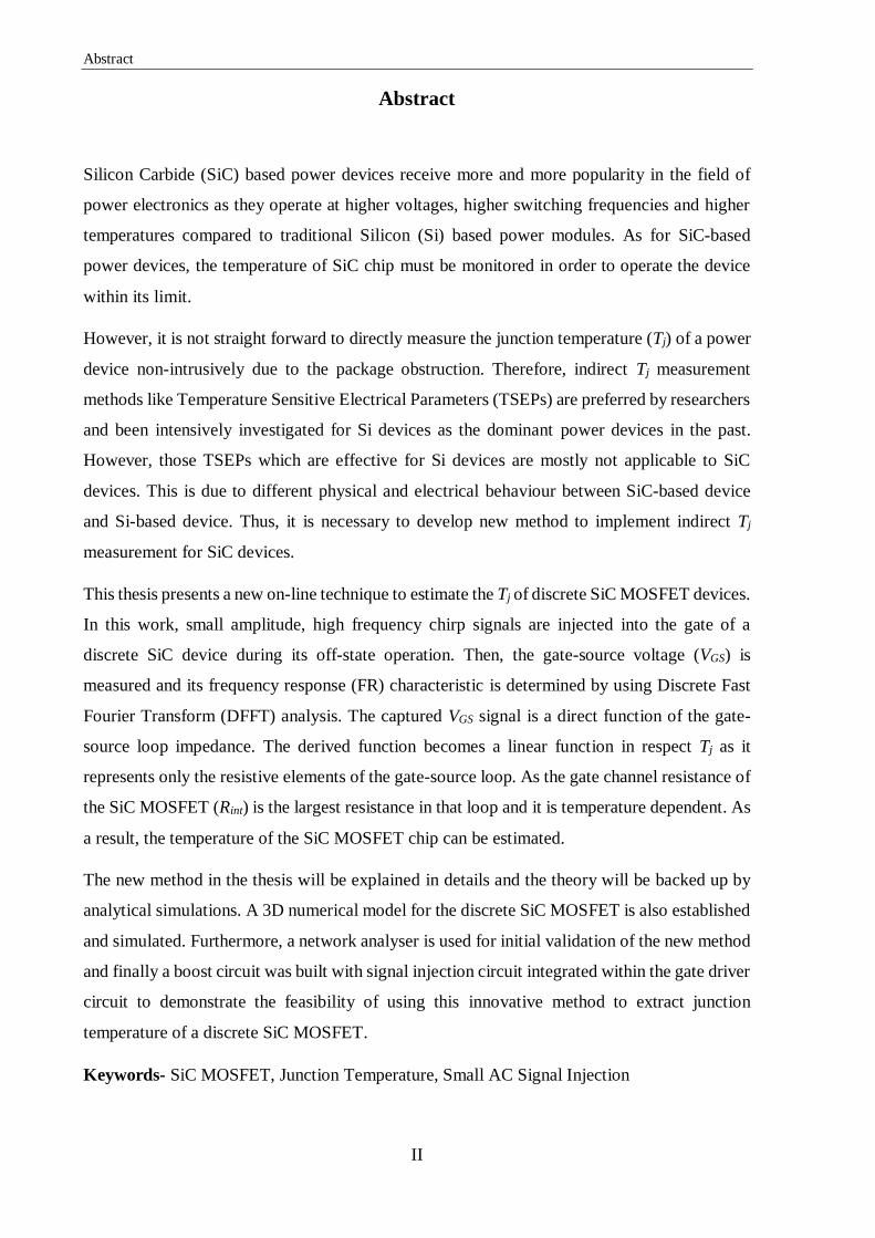
a. Model-based estimation of Tj
Analysis based on simplified electrical and thermal models in conjunction with the
semiconductor datasheet values is one of the classic ways to estimate the value of Tj. Usually,
the average junction temperature (Tj_avg) can be estimated via stationary thermal models taking
into consideration the thermal resistances and capacitances [6]. It is also possible to determine
the junction temperature swing (∆Tj) and even the maximum junction temperature (Tjmax) if
non-stationary conditions are assumed. An example of the Tj profile of a power device is
presented in Figure 1.2. The value of ∆Tj depends on the total power dissipation generated by
the device and the thermal impedance of the circuit, the range of the ∆Tj can vary from several
milli-degrees to several tens of degrees.
Figure 1. 2 An example of Tj profile of a power electronic device.
Although such modelling methods based on the manufacturer data have been extensively
utilized [7], these techniques are limited due to poor accuracy. This is because the thermal
values given by the manufacturer usually take into account the worst-case scenarios and may
not be appropriate for different topologies.
A more critical problem is that the thermal and electrical parameters of a power device or
module will change due to the degradation of the converter [8, 9], which will make the
estimation even more inaccurate given the degradation of the power device or module.
b. Temperature sensors embedded in the device
Due to the obstacles of module packaging and dielectric gel, it is not possible to directly gain
access to chips, which prevents optical and physical solutions for the measurement of
temperature such as by using infrared cameras or optical fibres. Thus, alternative methods have

Chapter 1 Introduction
3
been proposed to integrate temperature sensors within the power chip structure. Such industrial
applications have been implemented; for instance, Moto and Donlon [10] fabricated a string of
diodes on the surface of the IGBT chip and utilized the linear relationship between the forward
voltage drop of the string diodes and the temperature to estimate the value of Tj of the IGBT
chip. However, this method can only provide a local temperature measurement, which means
it cannot reflect the thermal gradient of the whole chip and is not able to determine the peak
temperature where degradation is most likely to appear [7]. A solution with multi-temperature
sensors has been proposed [11] which gives the global surface temperature of the chip.
However, extra wires are required for connections to the sensors to acquire the data and this
method still requires some modification of the chip surface, which is not desirable.
c. Temperature-sensitive electrical parameters
Over the past few decades, intensive research has been conducted to investigate the relationship
between Tj and inherent electrical parameters that depend on it. Those electrical parameters are
called temperature-sensitive electrical parameters (TSEPs) [12]. State-of-the-art TSEPs have
been summarized [12] and are discussed in detail in chapter 3. These studies reveal the potential
of using TSEPs to precisely extract Tj during the operation of a converter for traditional Si IGBT
or MOSFET. However, the requirement to modify the converter structure or its control strategy
to accomplish the TSEP measurement circuit or measuring time window can be seen as serious
issues in real applications.
1.2 Wideband-gap semiconductor
In order to increase power-density and reduce size, Si semiconductor devices are being replaced
with wideband-gap (WBG) semiconductors like silicon carbide (SiC), Gallium Nitride (GaN)
or diamond (C). WBG power switching modules promise the potential to switch at higher-
power, and they have higher-temperature capability, better thermal conductivity and faster
switching speeds. Some key characteristics of WBG semiconductors have been reviewed and
compared with Si [13].
Among these WBG semiconductors, discrete SiC MOSFETs have been successfully
manufactured by several companies and are now commercially available [14]. As with Si power
switching modules, knowledge of Tj is equally important. In fact, SiC MOSFETs can operate
at much higher temperatures, and so temperature swings and therefore stresses on the different

Chapter 1 Introduction
4
layers that form the SiC power switching module are much greater. However, the
aforementioned Tj measurement methods can hardly be applied to discrete SiC MOSFETs [15].
The difficulties of extracting Tj value for discrete SiC MOSFET has encouraged the author to
investigate a new method to measure Tj for discrete SiC MOSFETs online.
1.3 Objectives
1. Examining TSEPs that applicable for Si device on discrete SiC MOSFET to gain thorough
understanding of the behaviour of those TSEPs for SiC-based electronic devices.
2. Establishing a precise small AC signal equivalent circuit to enable simulation for discrete
SiC MOSFET and study the its off-state operation.
3. Creating 3D thermal model of SiC MOSFET and utilizing FEM software to determine the
internal Tj rise caused by power dissipation. The aim is to calibrate the actual Tj with the
measured Tj in the experiments in order to reduce errors.
4. Propose the new method to determine Tj of discrete SiC MOSFET based on analysis carried
out as indicated in point 1, 2 and 3.
5. Conducting practical experimental to validate the method developed.
1.4 Contribution to knowledge
The main original contribution of this research are as follows:
State-of-the-art Tj measurement methods for Si power devices are examined on discrete
SiC MOSFET to check the viability of those methods. And it turns out that those
methods have their limits to be applied to SiC-base devices.
The use of small AC signal analysis as a method to accurately extract the junction
temperature for SiC MOSFETs is proposed for the first time.
A small AC signal equivalent circuit of a Cree 2rd generation discrete SiC MOSFET is
developed for an unbiased SiC MOSFET. The model includes all individual parasitic
factors and all parameters have been calculated. The designed small AC signal
equivalent circuit has been simulated.
The gate-source impedance curve for an unbiased SiC MOSFET is measured as a
function of temperature using a network analyser. The results are compared with the
small AC signal equivalent circuit model for validation purpose.

Chapter 1 Introduction
5
The proposed AC sweeping technique is implemented in an existing SiC MOSFET gate
drive circuit applied to a biased SiC MOSFET. It is shown by experiment that the
proposed technique can detect the temperature of the chip with an error of 5%.
The proposed technique is implemented and validated in practical work.
The work conducted has resulted in the following publications:
[1] L. Xiang, C. Chen, M. Al-Greer, V. Pickert, and C. Tsimenidis, "An investigation of
frequency response analysis method for junction temperature estimation of SiCs power
device," in 2018 IEEE 10th CIPS conference.
[2] L. Xiang, C. Cuili, M. Al-Greer, V. Pickert, and C. Tsimenidis, "Signal processing
technique for detecting chip temperature of SiC MOSFET devices using high frequency
signal injection method," in 2017 IEEE 3rd International Future Energy Electronics
Conference and ECCE Asia (IFEEC 2017 - ECCE Asia), 2017, pp. 226-230.
The author has also contributed to the following research:
[3] C. Chen, V. Pickert, M. Al-Greer, C. Tsimenidis, T. Logenthiran, X. Lu, "Signal
sweeping technique to decouple the influence of junction temperature and bond wire
lift-off in condition monitoring for multichip IGBT modules," in 2018 IEEE 10th CIPS
conference.
1.5 Thesis outline
This thesis consists of six chapters. Chapter 1 gives a brief introduction of the background to
the thesis, including state-of-the-art Tj detection technique for Si power electronic devices or
modules and the progress of WBG semiconductors as well as the importance of the
development of a corresponding Tj measurement solution.
In Chapter 2, a specific overview of the SiC MOSFET and some state-of-art junction
temperature measurement techniques are presented, including a detailed comparison between
Si and SiC semiconductors. To begin with, the physical characteristics of Si and SiC are
compared and the results show that the superior capabilities of SiC materials can potentially
break the performance ceiling of SiC semiconductors. Then the switching characteristics of
both Si and SiC devices are compared as well which suggests that those differences may lead
to difficulties in implementing Tj measurement. Then, several Tj measurement methods used to
implement for Si devices with similar packaging technologies are presented. These techniques
are divided into three classes: direct and indirect temperature measurement techniques and
thermal model-based approaches. The direct temperature measurement techniques can be listed
as follows: infrared thermal camera techniques, embedded temperature sensor methods and
diode-on-die temperature sensing methods. These techniques are intrusive, which means either

Chapter 1 Introduction
6
the devices or module should be opened, or modifications should be carried out during the
manufacturing process. These features therefore limit the application of direct temperature
measurement. On the other hand, indirect temperature measurement methods use the TSEPs to
estimate the Tj values of the devices or modules. State-of-the-art TSEP measurement techniques
are presented and compared and principal measurement circuit are plotted for each method. The
third measurement technique is the thermal model-based method. Both open-loop and close-
loop thermal models used for estimating Tj are explained. Finally, their advantages and
disadvantages are concluded and compared as well.
Chapter 3 presents a 3D model of a Cree/Wolfspeed discrete SiC MOSFET (part number:
C2M0080120D[16]) with TO247-3 packaging is created by using Autodesk Inventor 3D
computer-aided design software. The implementation of the 3D model is based on the
information provided by manufacturer’s datasheets including dimensions of each components
as well as materials of each parts. In addition, a 3D model of a heat plate which will be used in
the later experimental test is established as well and it is fully constrained at the bottom of the
SiC MOSFET. After successfully producing the 3D model, both models of the discrete SiC
MOSFET and the heat plate are imported into the ANSYS finite element analysis software to
perform thermal analysis. The main purpose of the thermal study is to determine the temperature
difference between the hottest die body and the case surface temperature. The temperature
difference will be used later to calibrate with the experimental results to reduce error.
Chapter 4 starts with simulation results for traditional TSEPs applied to the discrete SiC
MOSFET and the results suggests that these TSEPs are unsuitable for SiC MOSFET due to
either lower sensitivity or reduced Tj dependency. Therefore, the motivation for proposing a
new method to estimate Tj values for SiC MOSFET arises. The author proposes a new technique
to extract the Tj value of the SiC MOSFET by a technique which analyses using small AC signal.
An equivalent small AC signal circuit for a SiC MOSFET during its off-state is developed and
individual parasitic values are calculated as well. The proposed model is simulated in LTspice
and then the simulation results are compared the practical results with the help of an impedance
analyser. The results indicate a good alignment between the two sets of values.
Chapter 5 describes the experimental test for the estimation of Tj in a discrete SiC MOSFET by
using small AC signal analysis. The experimental circuits are explained in detail at first and
then experimental results under different DC bias conditions are presented and analysed. The
results show that the proposed method has promising potential to fulfil the capability to give
accurate estimations of the Tj values of SiC MOSFETs. In addition, Cree/Wolfspeed discrete
SiC evaluation board (part number: KIT8020-CRD-8FF1217P-1) is utilized to create a standard

Chapter 1 Introduction
7
non-synchronous boost converter with a Cree/Wolfspeed SiC Schottky diode (C4D20120D)
and a discrete SiC MOSFET (part number C2M0080120D). The proposed method is used
during normal operation of the boost converter, and the small AC chirp signal is superimposed
via the gate driver of the evaluation board. The results will be presented and analysed.
Finally, Chapter 6 summarizes the research work which has been carried out and the advantages
and disadvantages of the proposed method are discussed. Future work which can be carried out
afterwards to improve the proposed method is also recommended.

Chapter 2 Overview of SiC MOSFET and State-of-Art Tj Measurement Techniques
8
Chapter 2 Overview of SiC MOSFET and State-of-Art Tj Measurement
Techniques
Wideband-gap (WBG) semiconductor devices have become more and more attractive in power
electronics applications [17-19], due to their superior characteristics compared to silicon-based
semiconductors. The more efficient manufacturing of WBG devices has seen a drop in the cost
of making them and they are now attractive for mainstream use. The most popular device is the
discrete normally-off n-channel SiC MOSFET with break-down voltages ranging between
600 V and 1.2 kV. For example Cree introduced the 1.2 kV, 33 A SiC MOSFET in 2011 [20].
Other manufacturers like Rohm and POWEREX are also developing discrete SiC MOSFETs
[21-23].
2.1 Comparison of physical structure and characteristics of Si and SiC MOSFET
SiC-based power devices are becoming more and more popular as they provide the opportunity
to build power converters which are smaller and lighter. SiC MOSFETs have advantages over
Si MOSFETs due to the former’s physical material properties. As illustrated in Figure 2.7, SiC
material offer three main advantages over Si: firstly, higher band-gap energy and increased
electric field capacity resulting in higher voltage operation; secondly, extended thermal
conductivity and a higher melting point, which makes SiC applicable for higher temperature
operations; and thirdly, faster electron velocity, which gives SiC-based devices increased
switching frequencies compared to Si-based devices [24].

Chapter 2 Overview of SiC MOSFET and State-of-Art Tj Measurement Techniques
9
Figure 2. 1 Comparison of Si, SiC, and GaN material characteristics [18].
All of the five listed characteristics in Figure 2.7 can be described analytically. In the following
sections, the key equations in semiconductor physics are shown.
a. Energy Gap
The temperature and band-gap energy of semiconductor materials determine the intrinsic carrier
density ni, and the relationship between them is given by equation 2.1.
𝑛𝑖 = (2𝜋𝑘𝑇
ℎ2 )3
2⁄(𝑚𝑑ℎ𝑚𝑑𝑒)
34⁄ 𝑒𝑥𝑝 (
−(𝐸𝑐−𝐸𝑣)
2𝑘𝑇) (2.1)
where k and h represent the Boltzman’s and Planck’s constants respectively, T is the absolute
temperature, mde and mdh are the electron and hole effective masses respectively, and (Ec-Ev) is
the band-gap energy. Equation 2.1 shows that the influence of temperature on the intrinsic
carrier density weakens in cases of higher band-gap energy material. This is an important
characteristic that is favoured in high-temperature applications [25]. The bandgap of SiC is
3.2 eV and of Si is1.12 eV. Also, a higher band-gap energy results in a lower intrinsic carrier
density, which results in smaller leakage currents at the p-n junction. The relationship between
the leakage current of a p-n junction and the intrinsic carrier density is given by equation 2.2
[26]:
𝑗𝑠 = 𝑞𝑛𝑖2 (
𝐷𝑝
𝐿𝑝𝑁𝐷+
𝐷𝑛
𝐿𝑛𝑁𝐴) (2.2)
In equation 2.2, ND and NA are the donor and acceptor carrier densities respectively, Dp and Dn
are diffusion constants of the p and n regions respectively and Lp and Ln are the diffusion lengths
in the p and n regions.

Chapter 2 Overview of SiC MOSFET and State-of-Art Tj Measurement Techniques
10
b. Electric field
The n-drift region determines the breakdown voltage capability in a vertical MOSFET, and a
higher critical electric field provides the capability for it to withstand higher breakdown voltage.
SiC has a critical field of 2.2 MV/cm and for Si it is 0.25 Mv/cm. Equation 2.3 describe the
breakdown voltage of a p-n junction [26]:
𝑉𝐵𝐷 = 𝑠𝐸𝑐𝑟𝑖𝑡2
2𝑞𝑁𝐵 (2.3)
Where ɛs is the permittivity of the semiconductor, Ecrit is the critical electric field at breakdown
and NB is the doping concentration of semiconductor in the low-doped region.
The conductivity of the drift region is given by equation 2.4 [26]:
𝛿 = 𝑞𝜇𝑛𝑁𝐷 (2.4)
Where μn is the electron mobility, ND is doper concentration and to be specified in the n drift
region. Assuming ND=NB, the equation 2.3 and equation 2.4 combine to become equation 2.5:
𝑉𝐵𝐷 =𝜇𝑛 𝑠𝐸𝑐𝑟𝑖𝑡
2
2𝛿 (2.5)
It can be interpreted from the above equation that a higher critical electric field makes it possible
to achieve higher conductivity at the same breakdown voltage.
c. Electron velocity
The theoretical channel transition time of the MOSFET is defined as the time that carriers
travelling in a channel at their saturation drift velocity vsat, and is represented by equation 2.6
[27]:
𝜏𝑡 =𝐿
𝑣𝑠𝑎𝑡 (2.6)
For SiC, vsat is 20 Mcm/V and for Si it is 10 Mcm/V [11].
The channel transition speed can also be described as the transition frequency 1/τt. Higher
saturation velocity means a higher transition frequency. For MOSFETs, theoretical transition
frequency cannot be achieved due to parasitic capacitance, and instead, the transition frequency
is given by equation 2.7 [27]:
𝑓𝑇 =1
2𝜋𝐶𝑖𝑠𝑠𝑅𝐺 (2.7)

Chapter 2 Overview of SiC MOSFET and State-of-Art Tj Measurement Techniques
11
where the Ciss is the input capacitance and it is the combination of the gate-source capacitance
CGS and gate-drain capacitance CGD. RG is the gate resistance which is a combination of external
gate resistance RGext and internal gate resistance RGint. Since the SiC MOSFET has smaller
parasitic capacitance in comparison with the Si MOSFET, the former can operate at higher
frequency.
d. Thermal conductivity
SiC has a thermal conductivity about 2 to 3 times higher than this property in Si material (SiC:
4 W/(cm ∙ K) Si: 1.5 W/(cm ∙ K) [11]). Equation 2.8 shows the relationship between thermal
conductivity and the amount of heat the material can dissipate [11]:
𝑘𝑡 =𝑄𝐿
𝐴∆𝑇 (2.8)
where kt is the thermal conductivity of the material, Q is the total amount of heat transfer
through the material in J/S or W, A is the surface area of the material body in cm2, L is the
length of the material body in cm, and ΔT is the temperature difference. As can be seen from
the equation, higher thermal conductivity enables SiC MOSFETs to dissipate heat more
efficiently, which makes it capable of working in higher temperature conditions.
e. Melting point
Assuming that all atoms in a crystal vibrate with the same frequency, ν, the average thermal
energy (E) can be estimated using the equipartition theorem [28] as follows:
𝐸 = 4𝜋2𝑚𝑣2𝑢2 = 𝑘𝑇 (2.9)
where m is the atomic mass, ν is the velocity, u is the average vibration amplitude, k is
the Boltzmann constant, and T is the absolute temperature. If the threshold value
of u2 is c2a2, where c is the Lindeman constant and a is the atomic spacing, then the melting
point is estimated as:
𝑇𝑚 =4𝜋2𝑚𝑣2𝑐2𝑎2
2𝑘𝐵 (2.10)
The melting temperature for SiC is around 2700 ˚C and for Si material is only 1400 ˚C. This
fact means that SiC material has the potential to operate in circumstance of much higher
ambient temperature.

Chapter 2 Overview of SiC MOSFET and State-of-Art Tj Measurement Techniques
12
2.2 Comparison of switching characteristics of Si and SiC MOSFETs
Due to the significant different material on-state and switching performance of SiC MOSFETs
and Si MOSFETs, the SiC material makes SiC MOSFETs superior in switching performance.
a. Non-linear on-resistance
One obvious difference between SiC and Si MOSFET is the temperature dependence of on-
state resistance (RDS(ON)) at different values of VGS. The relationships of RDS(ON) against
temperature are presented in [29] and the main results are shown in Figure 2.5. For a SiC
MOSFET RDS(ON) plotted versus temperature shows a U-shape curve in contrast to that for the
Si Cool MOSFET which shows a linear relationship with temperature.
Figure 2. 2 Comparison of on-state resistance versus temperature of Cool MOSFET and SiC MOSFET
at various gate voltages [29].
b. Negative turn-off gate voltage
Another characteristic difference in terms of gate drive considerations is the turn-off voltage
level. Due to the ultra-fast switching speed, a negative turn-off bias gate voltage (usually −2 to
−5 V) is recommended for the SiC MOSFET in order to increase the threshold margin and dv/dt
immunity, which would be helpful to avoid the false triggering in phase-leg operations [30].
Appendix B describes gate drive circuits for SiC MOSFETs in more detail.

Chapter 2 Overview of SiC MOSFET and State-of-Art Tj Measurement Techniques
13
c. Non-flattened Miller plateau
The much smaller Miller capacitance (CGD) of the SiC MOSFET also leads to different
switching characteristics in comparison with the Si MOSFET. One result of the smaller Miller
capacitance of the SiC MOSFET is a significantly faster VDS switching transient for the Si
counterpart. Another result is a non-flat Miller plateau [31], which means that the SiC MOSFET
will be less temperature-sensitive during the switching transient in comparison with the Si
MOSFET.
For power devices, it can be concluded that one of the fundamental causes of degradation is a
mismatch in the coefficients thermal expansion (CTEs) between the different layers in the
power module structures. CTE mismatch results in bond wire lift-off and solder cracks. Thus,
these particular thermo-mechanical effects lead to increase in chip temperature. Consequently,
the values of the device’s Tj represents information on power module degradation, and this
information can be used to detect forthcoming failures of power semiconductor modules.
However, the precise extraction of Tj values in real time is difficult and therefore has become a
hot topic in both academic and industrial research. The following section summarizes various
techniques that have been proposed in extracting Tj for Si power semiconductor devices, but
those techniques can be applied to SiC devices. It is because of SiC devices are still using those
packages used by Si devices which enables those Tj measuring techniques potentially viable for
SiC devices. The advantages and disadvantages of the different methods are also listed. A more
detailed description of some of the selected measurements is provided in Appendix A.
2.3 Direct temperature measurement techniques
There are three different methods used to measure chip temperature directly via an infrared
camera, a thermos-coupler attached to the die, and using a chip with an integrated
semiconductor temperature sensor.
a. Infrared thermal camera
For the bare die type or unpackaged power devices, it is viable to utilize an infrared (IR) thermal
camera [32]. The benefit of this is that this camera captures the temperature over the full device
surface allowing a thermal distribution map of the chip to be generated. A test bench utilizing
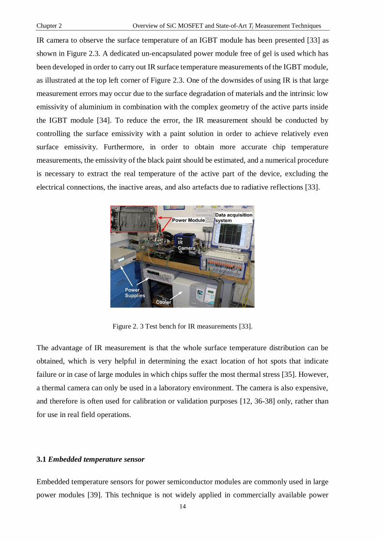
Chapter 2 Overview of SiC MOSFET and State-of-Art Tj Measurement Techniques
14
IR camera to observe the surface temperature of an IGBT module has been presented [33] as
shown in Figure 2.3. A dedicated un-encapsulated power module free of gel is used which has
been developed in order to carry out IR surface temperature measurements of the IGBT module,
as illustrated at the top left corner of Figure 2.3. One of the downsides of using IR is that large
measurement errors may occur due to the surface degradation of materials and the intrinsic low
emissivity of aluminium in combination with the complex geometry of the active parts inside
the IGBT module [34]. To reduce the error, the IR measurement should be conducted by
controlling the surface emissivity with a paint solution in order to achieve relatively even
surface emissivity. Furthermore, in order to obtain more accurate chip temperature
measurements, the emissivity of the black paint should be estimated, and a numerical procedure
is necessary to extract the real temperature of the active part of the device, excluding the
electrical connections, the inactive areas, and also artefacts due to radiative reflections [33].
Figure 2. 3 Test bench for IR measurements [33].
The advantage of IR measurement is that the whole surface temperature distribution can be
obtained, which is very helpful in determining the exact location of hot spots that indicate
failure or in case of large modules in which chips suffer the most thermal stress [35]. However,
a thermal camera can only be used in a laboratory environment. The camera is also expensive,
and therefore is often used for calibration or validation purposes [12, 36-38] only, rather than
for use in real field operations.
3.1 Embedded temperature sensor
Embedded temperature sensors for power semiconductor modules are commonly used in large
power modules [39]. This technique is not widely applied in commercially available power
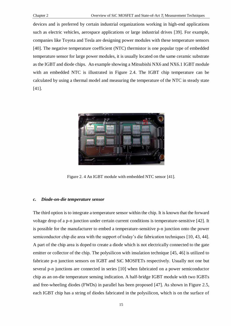
Chapter 2 Overview of SiC MOSFET and State-of-Art Tj Measurement Techniques
15
devices and is preferred by certain industrial organizations working in high-end applications
such as electric vehicles, aerospace applications or large industrial drives [39]. For example,
companies like Toyota and Tesla are designing power modules with these temperature sensors
[40]. The negative temperature coefficient (NTC) thermistor is one popular type of embedded
temperature sensor for large power modules, it is usually located on the same ceramic substrate
as the IGBT and diode chips. An example showing a Mitsubishi NX6 and NX6.1 IGBT module
with an embedded NTC is illustrated in Figure 2.4. The IGBT chip temperature can be
calculated by using a thermal model and measuring the temperature of the NTC in steady state
[41].
Figure 2. 4 An IGBT module with embedded NTC sensor [41].
c. Diode-on-die temperature sensor
The third option is to integrate a temperature sensor within the chip. It is known that the forward
voltage drop of a p-n junction under certain current conditions is temperature-sensitive [42]. It
is possible for the manufacturer to embed a temperature-sensitive p-n junction onto the power
semiconductor chip die area with the support of today’s die fabrication techniques [10, 43, 44].
A part of the chip area is doped to create a diode which is not electrically connected to the gate
emitter or collector of the chip. The polysilicon with insulation technique [45, 46] is utilized to
fabricate p-n junction sensors on IGBT and SiC MOSFETs respectively. Usually not one but
several p-n junctions are connected in series [10] when fabricated on a power semiconductor
chip as an on-die temperature sensing indication. A half-bridge IGBT module with two IGBTs
and free-wheeling diodes (FWDs) in parallel has been proposed [47]. As shown in Figure 2.5,
each IGBT chip has a string of diodes fabricated in the polysilicon, which is on the surface of

Chapter 2 Overview of SiC MOSFET and State-of-Art Tj Measurement Techniques
16
the IGBT chip’s emitter side. Chip temperature can be detected by measuring the forward
voltage drop when it is forward-biased. As with most silicon diodes, the forward voltage-drop
decreases with increasing Tj. To alleviate noise problems, a string of diodes is used to provide
a high enough sensing voltage. However, using the temperature sensing diode during
continuous switching operations is still challenging due to several facts listed below.
The first challenge is low forward voltage (VF) sensitivity, where low signal amplitude and
sensitivity make it vulnerable to noise which makes it hard to accurately sense Tj during
switching transients.
Figure 2. 5 IGBT module with on-die temperature sensing diodes [47].
The second issue is that, since the Tj sensing diodes are sited on the die area, the short distance
to sources of noise would induce noise propagation. The parasitic capacitances between the two
parallel IGBTs are likely to be larger than the NTC solution, as illustrated in Figure 2.6. A
displacement current incurred during the dv/dt switching transient may also affect the sensor’s
output signal, which will be even more critical in WBG devices. Moreover, these capacitance
values are difficult to measure directly as they are all interconnected with the device’s parasitic
capacitances.

Chapter 2 Overview of SiC MOSFET and State-of-Art Tj Measurement Techniques
17
Figure 2. 6 Parasitic capacitances between the sensing diode and power device [47].
Polysilicon with insulation technique has been utilized [45, 46] to fabricate p-n junction sensors
on IGBT and SiC MOSFETs respectively. Usually not one but several p-n junctions are
connected in series [10] when fabricated on a power semiconductor chip as an on-die
temperature sensing indicator.
Gate Driver
Shared Die Area
Voltage
SensorVF
Tj
Tj=ƒ(VF)
Figure 2. 7 Principal circuit for IGBT Tj sensing based on diode forward voltage.
As shown in Figure 2.7, in order to use the on-die diode as a Tj indicator, a constant current is
required to flow through the diode and then the voltage across the diode can be measured and
used for online Tj extraction. After proper correlation, the relationship between the diode

Chapter 2 Overview of SiC MOSFET and State-of-Art Tj Measurement Techniques
18
forward voltage drop and Tj can be established and in a previous study the sensitivity was
−6.7 mV/˚C [10].
This Tj sensing technique based on the diode forward voltage drop is capable of providing a
fast thermal-dynamic response to the semiconductor chip due to the small size of the diode
itself. Signal processing in this method is easy to implement as well, because only the forward
voltage is captured and only the relationship between the forward voltage VF and Tj. Tj is
required. A Fuji 7MBP50RA060 IGBT module using the above described method gave a 2 ms
response time for an over-temperature alarm [45],.
The sensing of Tj with a constant current source and voltage measurement [9] can be integrated
inside the power module. Although sharing the same die, the temperature-sensitive p-n junction
is isolated from the power semiconductor except for its capacitive coupling, which can limit its
usefulness during transients [11]. This is not the only limitation of this technique, and some
other issues have been identified. Firstly, the consistency of sensing can be challenging given
the limited number of diodes used for Tj sensing. As a result, the performance of the sensors
fabricated in the same batch can vary significantly [11]. Secondly, the on-chip p-n junction Tj
sensor is usually fabricated on a small area on the power semiconductor chip as shown in
previous studies [39, 41]. This location may not provide an accurate picture of the thermal
gradient of the chip. Thirdly, another issue is caused by the small size of the p-n junction in that
it is quite tricky to connect the relevant area to the measurement circuit via wire bonds or DBC,
and those wire bonds or DBC would also insert a certain amount of parasitic and contact
resistance as well [48]. Finally, the close location involved becomes a disadvantage when
considering that the performance of the sensing of Tj would be distorted by the noise generated
by the switching power semiconductor.
2.4 Indirect temperature measurement techniques
Over the last two decades a lot of researches have focused on the indirect measurement of Tj.
Rather than measuring the temperature directly, a relationship between voltage and current
signals measured at the gate, emitter and the source and the temperature is investigated. This is
because most semiconductor parameters, such as the on-state collector-emitter voltage of the
IGBT or the on-state resistance of the power MOSFET, are temperature-dependent.
Parameters that have a strong relationship with Tj are called temperature-sensitive electrical
parameters (TSEPs) [12]. TSEPs must fulfil minimum requirements in order to be used. These

Chapter 2 Overview of SiC MOSFET and State-of-Art Tj Measurement Techniques
19
requirements are firstly, that the parameters can be measured offline in order to determine the
relationship between the TSEP electric parameter of voltage or current and Tj. Secondly, the
measured relationship must be stored as reference. Thirdly, it must be possible to capture the
electrical parameter on the in-field power semiconductor module during operation and it must
be possible to compare the measurement with the stored reference. The reference will then
provide the Tj.
So far 20 different TSEPs have been proposed and the most promising TSEPs are those which
have a linear relationship between the monitored electric parameter and temperature. In addition,
TSEPs should have a fixed gradient, so that there is no change from positive to negative gradient
or vice versa over the entire temperature range. Furthermore, the gradient angle should be large
enough to provide for enough sensitivity to determine the correct temperature. Obviously, the
resolution of the sensors is important and must be considered in the entire TSEP chain. Finally,
the measurement itself should not disrupt the operation of the converter. The next sections
provide an overview of traditional TSEPs.
2.4.1 Component-on-die Tj extraction
Some components such as internal gate resistance that are located near the die area can be used
as an indication of the value of Tj, this method has the advantages that, since those components
are sitting extremely close to the die, thermal impedance and capacitance between the
semiconductor junction area and those temperature sensitive components are small which
means that the Tj sensing bandwidth is high.
a. Internal gate resistance as Tj indicator
The internal gate resistance can be used as an indicator of Tj in some IGBT and MOSFET chips,
as the internal gate resistors are located in the centre of the die in those chips and this variable
itself is temperature dependent. Tj can be estimated by measuring the value of internal gate
resistance [49, 50].

Chapter 2 Overview of SiC MOSFET and State-of-Art Tj Measurement Techniques
20
Gate Driver Shared Die Area
Voltage
Sensor
Vir Tj
Tj=ƒ(Vir)
Rext RintBA
Figure 2. 8 Principal circuit for internal gate resistor measurement.
A principal circuit for online internal gate resistor measurement is presented in Figure 2.8,
which is based on a previous study [49]. A constant measurement current is injected into the
Rint, which results in a voltage drop (Vir). The sensitivity of the measured voltage has been
reported to be 0.75 mV/˚C when this technique was applied to 6.5 kV IGBTs [49].
There are concerns about applying this Tj measurement concept utilizing internal gate resistor.
The first limitation is that, normally, point B in Figure 2.8 is not always accessible because it is
actually part of the semiconductor structure. The second concern is that a voltage sensor with
high resolution is required as the resistance changes only by several mΩ/˚C. Measurements at
larger voltages across the resistor are possible by injecting larger currents, but this would start
to heat up the device. The last point of concern is that switching noise from the power module
will interfere with the measurements as the voltage sensor must sit close to the die area [49].
2.4.2 Measurement of Tj during device on-state
Temperature dependent parameters during the device on-state have been developed to be a
viable choice and have been proposed several times in the literature; for example, using the
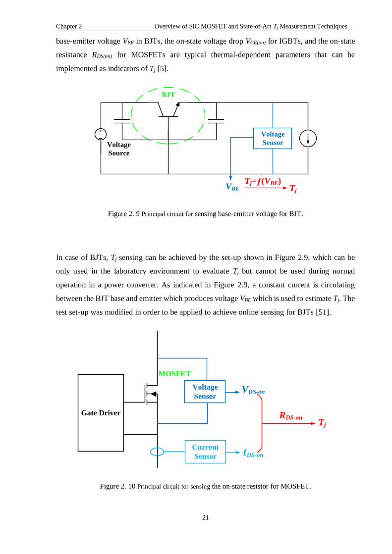
Chapter 2 Overview of SiC MOSFET and State-of-Art Tj Measurement Techniques
21
base-emitter voltage VBE in BJTs, the on-state voltage drop VCE(on) for IGBTs, and the on-state
resistance RDS(on) for MOSFETs are typical thermal-dependent parameters that can be
implemented as indicators of Tj [5].
BJT
Voltage
Sensor
VBE Tj
Tj=ƒ(VBE)
Voltage
Source
Figure 2. 9 Principal circuit for sensing base-emitter voltage for BJT.
In case of BJTs, Tj sensing can be achieved by the set-up shown in Figure 2.9, which can be
only used in the laboratory environment to evaluate Tj but cannot be used during normal
operation in a power converter. As indicated in Figure 2.9, a constant current is circulating
between the BJT base and emitter which produces voltage VBE which is used to estimate Tj. The
test set-up was modified in order to be applied to achieve online sensing for BJTs [51].
Gate Driver
Voltage
SensorVDS-on
Tj
RDS-on
Current
Sensor IDS-on
MOSFET
Figure 2. 10 Principal circuit for sensing the on-state resistor for MOSFET.

Chapter 2 Overview of SiC MOSFET and State-of-Art Tj Measurement Techniques
22
For power MOSFETs, the on-state resistance RDS(on) is a valuable TSEP [52]. The power
MOSFET RDS(on) can be derived by measuring the on-state voltage VDS(on) and on-state current
IDS(on) [53] at the same time, as shown in Figure 2.10. After the measurements, the on-state
resistance can be calculated using Ohm’s law (equation 2.1):
𝑅𝐷𝑆(𝑜𝑛) =𝑉𝐷𝑆(𝑜𝑛)
𝐼𝐷𝑆(𝑜𝑛) (2.1)
Gate Driver
Voltage
SensorVce
Tj
Tj=ƒ(Vce,Ice)
Current
Sensor Ice
IGBT
Figure 2. 11 Principal circuit for sensing on on-state voltage for IGBT
An important TSEP for IGBTs is the on-state collector-emitter voltage, VCE, which has been
extensively described in the literature [54, 55]. It is also necessary to synchronize the
measurement to the collector-emitter current, ICE, as VCE is a function of current and Tj.
Consequently, a current sensor is required too, as shown in Figure 2.11. The values of Tj of
IGBT can be presented in a three-dimensional graph [55]. The temperature gradient of an IGBT
chip has been investigated previously [56].
The aforementioned Tj sensing is based on the RDS(on) for power MOSFET and the VCE for IGBT,
it is required to measure both the voltage across the device during the on-state and the current
flowing through it. The current flowing through the device can be directly measured at the phase
level in many applications. Under these scenarios, it is crucial to determine the precise period
of the device’s forward conduction and to avoid the measurement of the commutation between
the transistor and diode. Galvanic isolation is necessary for the voltage sensor, since it is directly
connected to the power terminals of the MOSFET/IGBT. When the power electronic
semiconductor is fully turned on, the voltage across the device is rather lower than 1V. However,
when the switching device is completely turned off, the high DC voltage will be providing

Chapter 2 Overview of SiC MOSFET and State-of-Art Tj Measurement Techniques
23
directly across the device as well as the voltage sensor. Therefore, a floating voltage sensor is
required with a strong voltage endurance ability and high resolution.
During the operation of the power converter, noise is generated which could interfere with the
precision of the Tj estimation method based on on-state parameters. The sensitivity of the on-
state voltage drop is usually only several mV/°C, which is vulnerable to the influence of noise
from the switching of the power semiconductor.
It is also important to accurately measure the on-state current for Tj estimation, utilizing on-
state temperature-dependent parameters. For example, it is clearly shown in equation 2.1 that
RDS(on) is directly linked to the on-state current, IDS(on), which means that any incorrect
measurement of the current would induce error in estimating the real value of Tj. Other than the
outside measurement limitation, there are some issues inside power semiconductor devices as
well which might weaken the accuracy of measurement. The parasitic resistance of both the
DBC and the bond wires would induce an extra voltage drop in addition to the on-state voltage
drop of the device [56, 57]. An overestimation of Tj might result. This estimation error could
be eliminated by establishing a detailed packaging module and calculating the influence of both
DBC and bond wire parasitic [58]. Aged or the failure of the bond wires may cause the
evaluation to be inaccurate when degradation appears [59].
The measurement of Tj based on on-state Tj-dependent parameters is applicable for simple
converter topologies like buck/boost converters. For multi-switch converter topologies,
multiple high-voltage and high-resolution voltage sensors need to be installed, which would
increase the size of the converter system as well as the overall costs. As explained above, the
voltage measurement circuit sits between the two power terminals of the power semiconductor,
which might also face thermal-mechanical and electromagnetic interference issues.
One advantage of this method is that data processing is rather easy to implement by a simple
digital computation of the measured on-state voltage and on-state current. The frequency of the
on-state current (load current) is much lower than the switching frequency, which means that
the on-state current can be seen as a constant within limited numbers of switching cycles. Under
these circumstances, there is no need for high-bandwidth current measurement for the load
current, and the Tj bandwidth will solely depend on the on-state voltage measurement
bandwidth [60].

Chapter 2 Overview of SiC MOSFET and State-of-Art Tj Measurement Techniques
24
2.4.3 Tj measurement during device switching transient
The measurement of Tj during the semiconductor switching transients is an alternative solution
in comparison to on-state Tj sensing. Basically, the device switching transients of device
currents and voltages vary either in rising or falling time, amplitude or delay depending on the
value of Tj and the TSEP parameter that is observed.
a. Switching transient methods based on time period
It is essential to implement accurate time counters to precisely measure a certain time period of
a switching event. The IGBT Miller plateau width of the gate emitter voltage VGE during the
turn-off transient has been reported to be an indicator of the value of Tj [61]. As presented in a
previous study [54],the relationship between the duration of Miller plateau and the IGBT Tj has
been estimated. The principal circuit for this is depicted in Figure 2.12. The measured IGBT
gate-emitter voltage during the turn-off period requires a threshold voltage detector in order to
detect when the Miller plateau begins, and it requires a counter counting the length of time of
the plateau. The sensitivity of the Miller plateau width can vary from 0.8 ns/°C to 3.4 ns/°C
for different IGBT modules.
Gate Driver
Voltage
SensorVGE
Tj
Tj=ƒ(Time Span)
IGBT
Peak Detector
+
Time Counter
Time Span
Figure 2. 12 Principal circuit for the detection of Miller plateau width during turn-off transient.

Chapter 2 Overview of SiC MOSFET and State-of-Art Tj Measurement Techniques
25
In the IGBT module, there are two emitters. One is the power emitter “E” and the other is the
Kelvin emitter “e”. The voltage between the two emitter terminals (VeE) can also be used as an
indicator of Tj [62]. Two spikes with amplitudes of 3 V and 5 V respectively appear during the
IGBT turn-off transient in the VeE [55]. It has been claimed that the time span (also referred as
“VeE delay time”) between the two spikes is sensitive to Tj in the IGBT module [62, 63]. Figure
2.13 illustrates the principal measurement circuit for online measurement. The measured VeE
data is analysed by a pulse detector and a time counter and, as a result, the VeE delay time can
be determined. The variation in the VeE delay is 8 ns/°C.
Gate
Driver
Voltage
Sensor
Tj=ƒ(VeE delay)
VeE delay
IGBT
Kelvin
Emitter
Kelvin
Emitter
Power
Emitter
Pulse Detector
+
Time Counter
Tj
Figure 2. 13 Principal circuit to measure VeE delay time.
The IGBT switching transient period during turn-on and turn-off are reported to both be
sensitive to Tj [64, 65]. The turn-off time of the IGBT can be utilized to estimate the IGBT Tj
online, and has been illustrated that with the increment in value of Tj, smaller dVCE/dt and longer
turn-off time can be detected [66, 67]. The principal measurement set-up is shown in Figure
2.13. By processing the VCE data captured by the voltage using the threshold detector and time
counter, the turn-off time of the IGBT can be extracted. The sensitivity of the IGBT turn-off
time would change from 3 to 4 µs/°C depending on different values of DC bus voltage and load
current [67].

Chapter 2 Overview of SiC MOSFET and State-of-Art Tj Measurement Techniques
26
Gate Driver
Voltage
SensorVCE
Tj
Tj=ƒ(Switching Time )
IGBT
Amplitude
Detector
+
Time Counter
Switching Time
Figure 2. 14 Principal Tj measurement of the voltage switching times.
There are various requirements for these three aforementioned methods in order for them to be
realized. Firstly, they require high bandwidth voltage comparators (1 GHz minimum), and
secondly, they require high resolution time counters (1 ns/step). The measurement circuitry of
the proposed Miller plateau method [61] can be integrated in the gate driver since it measures
VGE. According to another study [62], the VeE delay time requires access to both the Kelvin
emitter and power emitter, which means that the sensing circuitry must be located very close to
the power module. Galvanic connection between the IGBT collector and emitter is necessary
for the method to measure the switching times as proposed [67].
b. Tj measurement based on amplitude of temperature-sensitive electrical parameters
Measurement of the amplitude of specific voltages and currents as TSEPs have been reported
for Tj [68]. For example, it has been claimed that the IGBT short-circuit current, ISC, can be used
to estimate Tj [61]. Results [68] have shown that the value of ISC is not vulnerable to device
voltage stress, gate drive voltage, or load condition. As shown in Figure 2.15, a short-circuit
pulse is created to enable the measurement of ISC. A sensitivity of 0.17%/°C has been reported
[61]. The short circuit current can be measured by a current transducer, which is a non-intrusive

Chapter 2 Overview of SiC MOSFET and State-of-Art Tj Measurement Techniques
27
measurement. However, the downside of this is that frequent short-circuit pulse injection could
accelerate device degradation which has also been pointed out [68].
Gate Driver
Tj
Tj=ƒ(Vce,Ice)
Current
Sensor Isc
IGBT
Figure 2. 15 Principal circuit for short-circuit Tj measurement.
The voltage between the Kelvin emitter and the power emitter VeE has once again been proposed
as a Tj measurement indicator [69]. Instead of investigating the VeE delay time between two
voltage pulses, the amplitude of the bigger pulse during the turn-off process has been studied
[62]. As shown in Figure 2.16, the VeE peak is measured by a peak detector and then correlated
with the corresponding IGBT Tj.
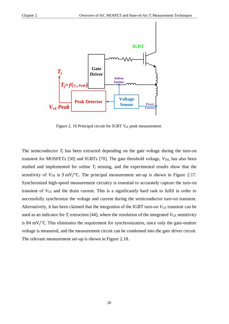
Chapter 2 Overview of SiC MOSFET and State-of-Art Tj Measurement Techniques
28
Gate
Driver
Voltage
Sensor
Tj=ƒ(VeE Peak)
VeE Peak
IGBT
Kelvin
Emitter
Kelvin
Emitter
Power
Emitter
Peak Detector
Tj
Figure 2. 16 Principal circuit for IGBT VeE peak measurement.
The semiconductor Tj has been extracted depending on the gate voltage during the turn-on
transient for MOSFETs [50] and IGBTs [70]. The gate threshold voltage, VTH, has also been
studied and implemented for online Tj sensing, and the experimental results show that the
sensitivity of VTH is 3 mV/°C. The principal measurement set-up is shown in Figure 2.17.
Synchronized high-speed measurement circuitry is essential to accurately capture the turn-on
transient of VGS and the drain current. This is a significantly hard task to fulfil in order to
successfully synchronize the voltage and current during the semiconductor turn-on transient.
Alternatively, it has been claimed that the integration of the IGBT turn-on VGE transient can be
used as an indicator for Tj extraction [44], where the resolution of the integrated VGE sensitivity
is 84 mV/˚C. This eliminates the requirement for synchronization, since only the gate-emitter
voltage is measured, and the measurement circuit can be condensed into the gate driver circuit.
The relevant measurement set-up is shown in Figure 2.18.

Chapter 2 Overview of SiC MOSFET and State-of-Art Tj Measurement Techniques
29
Gate Driver
Voltage
SensorVGS
ID
Current
Sensor
Tj
Tj=ƒ(VTH)
Syn
chro
niz
atio
n
VTHMOSFET
Figure 2. 17 Principle circuit for MOSFET VTH measurement.
Gate Driver
Voltage
SensorVGE
Tj
Tj=ƒ(ʃ VGE )
IGBT
Integrator
+
Time Counter
ʃ VGE
Figure 2. 18 Principle circuit of integration of VGE measurement.
It is known that TSEPs can affect the dynamic characteristics of both the switching power
electronic devices and their gate driver systems. This means that some of the gate driver output
parameters can be dependent on Tj. For instance, the gate drive output current during the turn-
on transient can be selected as an indicator of Tj for Si MOSFET [71], the Si IGBT [72] and the
GaN HEMT [73]. The Tj measurement circuit can be integrated within the gate driver circuit
and there will be no intrusive access needed for power semiconductors. The measurement
circuits for the MOSFET gate current peak (IGpeak) and IGBT gate current integration (ƒIGpeak)
are illustrated in Figures 2.19 and Figure 2.20 respectively.
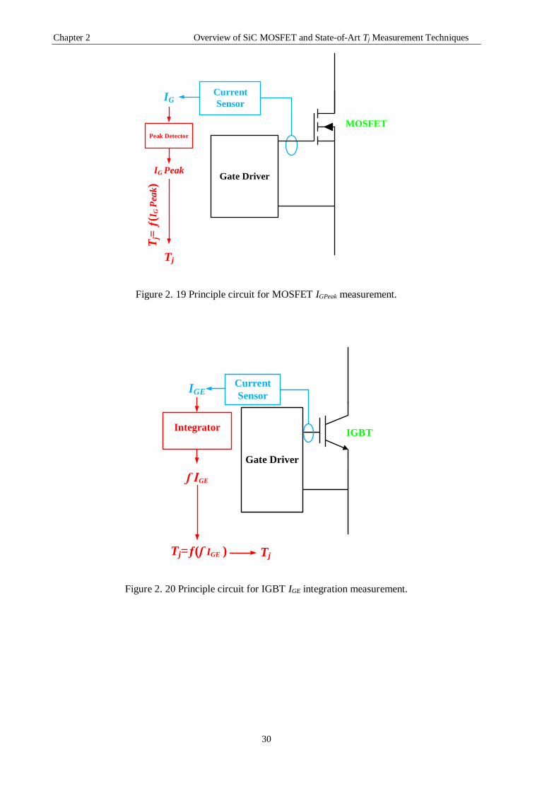
Chapter 2 Overview of SiC MOSFET and State-of-Art Tj Measurement Techniques
30
Gate Driver
Tj
Tj=
ƒ(I
G P
eak)
MOSFET
Current
SensorIG
Peak Detector
IG Peak
Figure 2. 19 Principle circuit for MOSFET IGPeak measurement.
Gate Driver
TjTj=ƒ(ʃ IGE )
IGBT
ʃ IGE
Current
SensorIGE
Integrator
Figure 2. 20 Principle circuit for IGBT IGE integration measurement.

Chapter 2 Overview of SiC MOSFET and State-of-Art Tj Measurement Techniques
31
2.4.4 Thermal model based Tj acquisition
Other than these TSEPs aforementioned in 2.3 and 2.4, knowledge of the thermal dynamic
model and power dissipation of the semiconductor chip can be used to estimate Tj [74]. The
switching losses and the conduction losses of the semiconductor form the total power
dissipation. Individually, both types of losses vary during switching [75]. Establishing the
device’s thermal dynamic model can be useful in order to analyse power dissipation and
consequently to estimate Tj [76]. A device Tj observer can be built for online Tj estimation by
analysing the information concerning the semiconductor device’s power dissipation with a
properly built thermal dynamic model. There are basically two types of Tj observers: open-loop
Tj and closed-loop Tj observers.
a. Methods based on an open-loop Tj observer
The voltage and current in conjunction with the Tj condition determine the switching losses of
the power semiconductor [77]. The device’s power losses Ploss_k need to be continuously
updated based on the device voltage Vk as measured during the on-state and off-state, the
current Ik flowing through the device, the duty ratio dk of the switching cycle and the estimated
value of Tj of the previous switching cycle, Tj_k-1. A cross-coupled model for power-dissipation
based on Tj estimation is simplified and represented in equations 2.2 and 2.3:
𝑃lossk= 𝐹(𝑉𝑘 , 𝐼𝑘 , 𝑑𝑘,𝑇𝑗𝑘−1) (2.2)
𝑇j_k = 𝐺(𝑇𝑗𝑘−1, 𝑃𝑙𝑜𝑠𝑠_𝑘) (2.3)
where F is the device’s loss model and G is its thermal dynamic model. It has been assumed
here that ambient temperature and convection at the device surface do not vary [77]. The
accuracy of the loss model F and the thermal dynamic model G would ultimately determine
the precision of this method.

Chapter 2 Overview of SiC MOSFET and State-of-Art Tj Measurement Techniques
32
PWM
Controller
Semiconductor
Power Module
Open-loop
Tj Observer
ik*
Vk ˄
Vk
ik
Tjk
Tjk
˄
dk
Figure 2. 21 Tj estimation based on an open-loop observer.
PWM
Controller
Semiconductor
Power Module
Closed-loop
Tj Observer
ik*
Vk ˄
Vk
ik
Tjk
Tjk
˄
dk
Tfk
Figure 2. 22 Tj estimation based on a closed-loop observer.
The open-loop Tj observer can be established without measuring the device voltage, current,
and duty ratio. Instead, as shown in Figure 2.21, reference values (with superscript *) and
estimated values (with superscript ˄) are utilized in the loss model F as described in equation
2.4:
𝑃lossk= 𝐹(𝑉𝑘
∗, 𝐼𝑘˄, 𝑑𝑘,𝑇𝑗𝑘−1) (2.4)
This method has been implemented in different topologies [70, 78] . Another study [67], the
experiment has been conducted on a Mitsubishi Electric 2-in-1 IGBT module and the results
show that the Tj error is around 2 °C and feedback is provided with a 2 ms delay.

Chapter 2 Overview of SiC MOSFET and State-of-Art Tj Measurement Techniques
33
The weakness of the open-loop observer method is that accuracy solely depends on the device
loss model and the thermal dynamic model since there is no Tj feedback, and so the accuracy
will be significantly affected by any thermal disturbance.
b. Method based on closed-loop Tj observer
As shown in Figure 2.22, the open-loop Tj observer can be optimized by imposing feedback
signals from the power semiconductor; for example, as shown in equation 2.5, the module base-
plate temperature, DBC temperature, and so on can be used as a feedback signal Tf.
𝑇𝑗_𝑘 = 𝐺(𝑇𝑗𝑘−1, 𝑇𝑓𝑘−1, 𝑃𝑙𝑜𝑠𝑠_𝑘) (2.5)
An enhanced Luenburger style Tj observer which use the baseplate temperature as the feedback
signal has been proposed and has been applied on a 1200 V/150 A Fuji IGBT [79]. The IGBT
Tj was controlled within a ±15 °C range of the desired temperature. The temperature feedback
signal can be measured by using an isolated temperature sensor which will either be intrusive
(DBC temperature sensor) and non-intrusive (base-plate temperature sensor).
The power loss model F is claimed to be influenced by device age [80, 81]. It has been shown
[81], that the IGBT on-state voltage VCE can be 13% bigger than the value when the device is
healthy after 100,000 power cycles. For the open-loop Tj observer, this effect induced by
degradation cannot be justified and consequently error would appear in estimating the value of
Tj. In the case of a closed-loop observer, a feedback signal could be helpful in correcting the
error.
2.5 Conclusion
In the beginning of this chapter, the physical and electrical behaviour of Si and SiC materials
are compared. It shows that SiC-based power devices have lots of advantages over traditional
Si-based power devices and enable SiC-based devices have the potential to replace Si-base
devices in near future. It is important to monitor the Tj of SiC devices because they have the
ability to be operated at much higher ambient temperature than Si devices. Thus, it is important
to summarize the state-of-the-art methodologies that have been proposed to capture Tj online
for power semiconductors. Additionally, principal measurement set-ups have been illustrated
for each method. It has been concluded that for discrete SiC MOSFET, only indirect Tj

Chapter 2 Overview of SiC MOSFET and State-of-Art Tj Measurement Techniques
34
measurement methods could potentially be applied. In later chapter 4, preferred indirect Tj
measurement methods which have been successfully applied to Si devices, especially methods
that utilizing TSEP, will be used onto discrete SiC MOSFET in order to exam whether those
methods can be employed on SiC-base devices or not.

Chapter 3 3D Thermal Model Establishment and FEM Thermal Simulation
35
Chapter 3 3D Thermal Model Establishment and FEM Thermal
Simulation
The previous chapter summarized the physical and electrical behaviours of the SiC materials
and highlighted the difference between the Si-based devices and SiC-based devices. It can be
concluded that the SiC-based devices have better performance over the Si-based devices. SiC-
based devices are becoming preferred for applications that require extremely high reliability,
because the fact that the SiC device can be operated under much higher temperature and much
harsher environment. Which means that it is important to supervise the health condition of the
SiC-base devices. However, the literature review regarding the state-of-art junction temperature
detection technique reveals that current techniques are not suitable for discrete SiC devices.
Those techniques either need modification to the device itself which is not suitable for discrete
device or they cannot be applied to SiC device due to SiC’s unique physical and electrical
attributes. Under this circumstance, it is viable to do further investigation in terms of the thermal
behaviour of SiC MOSFET.
In this chapter, in order to further investigate the thermal behaviour and temperature distribution
of the SiC MOSFET, a 3D thermal model of the C2M0080120D SiC MOSFET is established
using Autodesk inventor.
3.1 Establishing 3D Thermal Model
The reason why it is important to investigate the thermal performance of the SiC MOSFET
package is that this simulation could be helpful to precisely estimating the junction temperature
rise induced by the combination of conduction losses and switching losses during operation. As
a result, the true junction temperature can be derived to reduce the error of measured
temperature which would influence the accuracy of the final collaboration.
The first step of building up a 3D model is to create the outer structure of the object under study.
And it is crucial to using accurate data to construct the object. The SiC MOSFET is using
TO247-3 package and the dimensions of the package has been presented in Fig 3.1 below
provide by Wolfspeed[16].

Chapter 3 3D Thermal Model Establishment and FEM Thermal Simulation
36
Figure 3. 1 TO247-3 Package outer dimension.
The second step is to create the inner content of the object. In this case, it is basically the inner
bare die and the bond-wires. The dimension of the inner die can be found in the Wolfspeed
C2M0080120D bare die datasheet as shown in Fig 3.2. The dimension information is also
summarized in table 3.1.

Chapter 3 3D Thermal Model Establishment and FEM Thermal Simulation
37
Figure 3. 2 C2M0080120D bare die dimension graph.
Table 3. 1 C2M0080120D bare die parameter and material of each components
Parameter Typical Value Unit
Die Dimensions (L x W) 3.10 × 3.36 mm
Exposed Source Pad Metal Dimensions (LxW) Each 1.04 × 1.43 mm
Gate Pad Dimensions (L x W) 0.80 × 0.50 mm
Die Thickness 180 ± 40 µm
Top Side Source metallization (Al) 4 µm
Top Side Gate metallization (Al) 4 µm
Bottom Drain metallization (Ni/Ag) 0.8 / 0.6 µm
The final step is to assemble all the pieces created above with correct constrain condition and
then allocate materials for each part of the object accordingly base on their attributions indicated
in the datasheet. The bill of materials (BOM) is provided by the manufacturer.
The major difficulty of establishing the 3D model is the accuracy of the position of each
component especially the exact position of the bare die. In this simulation process, the bare die

Chapter 3 3D Thermal Model Establishment and FEM Thermal Simulation
38
is assumed to be allocated at the centre of the TO-247-3 package. And the gate pad is sitting at
the left of the bare die pad while the source pad and drain pad are located at the right-hand side
of the bare die pad, which is a common arrangement for TO247-3 discrete MOSFET.
Figure 3.3 shows the established 3D model of C2M0080120D with a heat plate underneath it
by using Autodesk inventor. Fig 3.3 (a) shows the full image of the SiC MOSFET with straight
leads.
Fig 3.3 (b) presents the internal view of the SiC MOSFET when the top capsule is removed. It
can be seen that the bare die is sitting at the middle of the package and the drain pad at the
bottom of die is directly attached to the drain terminal metal. While the gate pad and two source
pads are connected to the gate leads and sources leads respectively. At last, Fig 3(c) gives a
close view of the bare die.
(a)
(b)

Chapter 3 3D Thermal Model Establishment and FEM Thermal Simulation
39
(c)
Figure 3. 3 3D thermal model of C2M0080120D SiC MOSFET with heat plate: (a) complete package
model, (b) internal view with top capsule removed, (c) bare die model.
3.2 3D Model Internal Power Loss Calculation
In order to precisely evaluate the internal losses generated by the MOSFET junction. It is
required to determine the total power losses of the MOSFET.
Power losses in the MOSFET of boost converter are basically due to the following contributors:
1. Conduction loss of MOSFET and 2. Turn on and turn off switching losses of MOSFET.
Conduction loss of MOSFET is due to the channel on state resistance or commonly known as
RDSon. RDSon is dependent to the applied gate-source voltage (VGS) and the junction temperature
as shown in the figure below from C2M0080120D datasheet[16].

Chapter 3 3D Thermal Model Establishment and FEM Thermal Simulation
40
Figure 3. 4 On-Resistance VS. Temperature for different gate source voltages.
It can be interpreted from Fig 3.4 that with the increase of the gate source voltage (VGS), the
RDSon reduces under each different operating temperature. To lower the conduction losses of the
MOSFET, the manufacturer would recommend users to use optimal VGS. In case for
C2M0080120D discrete SiC MOSFET, the recommended VGS is 20 volts. At 20V VGS, the RDSon
homogenously rise with the increment of temperature.
The conduction loss due to RDSon can be calculated by equation listed below:
𝑃lossRDSon = 𝐼𝐷𝑟𝑎𝑖𝑛2 × 𝑅𝐷𝑆𝑜𝑛 (3.1)
Where IDRAIN is the RMS drain current while RDSon is the correct on-state resistance considering
VGS and corresponding junction temperature. RDSon of the C2M0080120D SiC MOSFET at
different Tj conditions are summarized in table 3.2 below.
Table 3. 2 On-state resistance at different junction temperature conditions.
Junction Temperature (°C) On-state Resistance (mΩ)
25 109
50 111
75 116
100 120
125 129

Chapter 3 3D Thermal Model Establishment and FEM Thermal Simulation
41
Figure 3. 5 Typical boost converter topology used for MOSFET power loss calculation.
Considering below boost circuit in Fig 3.5, the RMS drain current is can be computed using
below equation:
𝐼𝑅𝑀𝑆𝐹𝐸𝑇=
𝑑𝑖√𝐷
√3+ √𝐷 × (𝐼𝑚𝑎𝑥 − 𝑑𝑖)2 (3.2)
Where
𝐼𝑚𝑎𝑥 =2×𝐼𝑜𝑢𝑡+𝑑𝑖×(1−𝐷)
2×(1−𝐷) (3.3)
𝑑𝑖 =𝐷×𝑉𝑖𝑛
𝐿×𝐹𝑠𝑤 (3.4)
𝐷 =𝑉𝐷−𝑉𝑖𝑛+𝑉𝑜𝑢𝑡
𝑉𝐷+𝑉𝑜𝑢𝑡−𝑉𝑆 (3.5)
Where Iout is the DC load current of the boost converter, Fsw is the switching frequency of the
MOSFET, di is the inductor current ripple, L represents the boost inductor, Vin is the input
voltage, VD is forward drop of the diode, VS is the voltage drop of the MOSFET during on-state
and Vout is the output voltage. The value of the passive components in Fig 3.5 has been
summarized in Table 3.3 below.
Table 3. 3 Passive components summary of boost converter.
Passive Components Value (Unit)
Boost Inductor (L) 75 (uH)
Input Capacitor (Cin) 300 (uF)
Output Capacitor (Cout) 600 (uF)
Load Resistor (R) 30-300 (Ω)
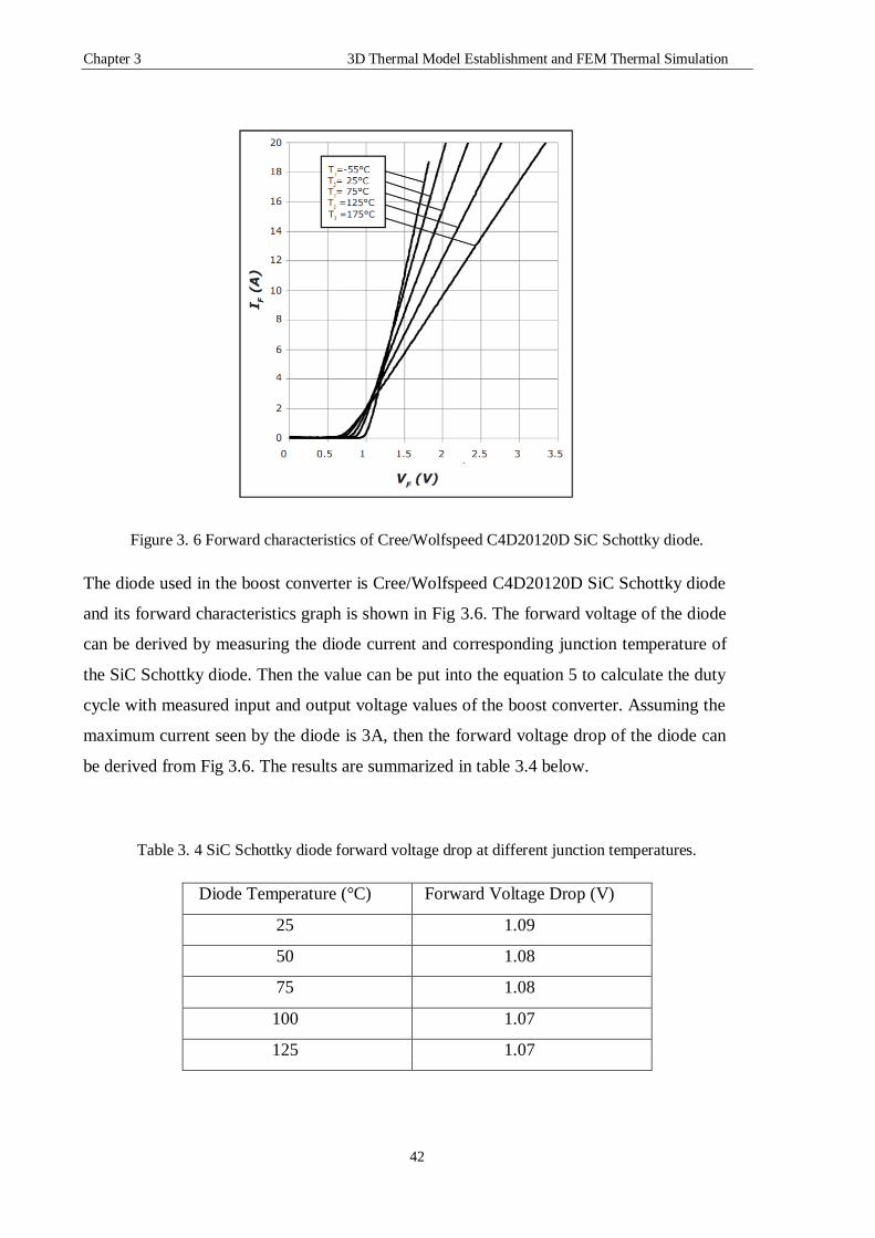
Chapter 3 3D Thermal Model Establishment and FEM Thermal Simulation
42
Figure 3. 6 Forward characteristics of Cree/Wolfspeed C4D20120D SiC Schottky diode.
The diode used in the boost converter is Cree/Wolfspeed C4D20120D SiC Schottky diode
and its forward characteristics graph is shown in Fig 3.6. The forward voltage of the diode
can be derived by measuring the diode current and corresponding junction temperature of
the SiC Schottky diode. Then the value can be put into the equation 5 to calculate the duty
cycle with measured input and output voltage values of the boost converter. Assuming the
maximum current seen by the diode is 3A, then the forward voltage drop of the diode can
be derived from Fig 3.6. The results are summarized in table 3.4 below.
Table 3. 4 SiC Schottky diode forward voltage drop at different junction temperatures.
Diode Temperature (°C) Forward Voltage Drop (V)
25 1.09
50 1.08
75 1.08
100 1.07
125 1.07

Chapter 3 3D Thermal Model Establishment and FEM Thermal Simulation
43
There is an interesting point need to be addressed is that forward characteristic of the SiC
Schottky diode (C4D20120D) used in the calculation presents a knee area. It means that
when the forward current is lower than about 6A the forward voltage drop shows a
decreasing trend when the junction temperature of the diode increase. While when the
forward current is higher than 6A, the forward voltage-drop of the SiC Schottky diode
present an opposite behaviour that with the increasing of the junction temperature the
forward voltage drop increase.
The voltage-drop of the SiC MOSFET during turn-on can be also determined by looking up
the datasheet graph. Under 3A drain-source current condition, the VS is 0.275V. Other input
parameters are listed below: the input voltage is 15V, the output voltage is 50V and the
switching frequency of the SiC MOSFET is 20KHz. Assign all the input parameters into
equation (3.5), and then the duty cycle D can be calculated to be 71%. The inductor current
ripple can be also calculated by substituting values in equation (3.4) and the result is 7.1A.
The output resistance is tuned to be 100ohm during the test, thus the output current can be
derived as 50V/100ohm equals to 0.5A. By substituting values of Iout, di and D into equation
(3.3), the maximum current can be determined and result for Imax is 5.27A. The next step is
assigning all calculated results in equation (3.2), the RMS current can be found, and it equals
to 3.75A. Finally, the conduction loss can be computed using equation (3.1). The result of
conduction loss is summarized as below: under 25°C junction temperature condition and
3.75A RMS drain current, the conduction loss is 1.53W; under 50°C junction temperature
condition and 3.75A RMS drain current, the conduction loss is 1.56W; under 75°C junction
temperature condition and 3.75A RMS drain current, the conduction loss is 1.63W; under
100°C junction temperature condition and 3.75A RMS drain current, the conduction loss is
1.69W and under 100°C junction temperature condition and 3.75A RMS drain current, the
conduction loss is 1.82W.

Chapter 3 3D Thermal Model Establishment and FEM Thermal Simulation
44
Figure 3. 7 Typical characteristics of power MOSFET switching transients.
Switching losses of MOSFET during turn on and turn off are associated with the rise and
fall time of the MOSFET. Switching time measurement circuit and input/output waveform
are shown below in Fig 3.7.
Where td(on) is turn-on delay time: the time from when the gate-source voltage rises above
10% of VGS until the drain-source voltage reaches 90% of VDS, tr is the rise time: the time
taken for the drain-source voltage to fall from 90% to 10% of VDS, tsw,on is the turn-on time:
the turn-on time is equal to td(on)+tr. While td(off) is turn-off delay time: the time from when
the gate-source voltage drops below 90% of VGS until the drain-source voltage reaches 10%
of VDS, tf is the fall time: the time taken for the drain-source voltage to rise from 10% to 90%
of VDS and tsw,off is turn-off time: the turn-off time is equal to td(off)+ tf.
The information of tr and tf of C2M0080120D SiC MOSFET is summarized in Table 3.5 as
below.
Table 3.5 turn-on time and turn-off time of C2M0080120D
Symbol Symbol Parameter Min. Typ. Max. Unit
td(on) Turn-on delay time - 11 -
ns tr Rise time - 20 -
tf(on) Turn-off delay time - 23 -
tf Fall time - 19 -

Chapter 3 3D Thermal Model Establishment and FEM Thermal Simulation
45
The switching losses of SiC MOSFET can be approximated by using the below equation:
𝑃loss_switching =1
2× (𝑡𝑟 + 𝑡𝑓) × 𝐼𝑅𝑀𝑆_𝐹𝐸𝑇 × 𝑉𝐷𝑆 × 𝐹𝑠𝑤 (3.6)
Where tr is the rise time, tf is the fall time, IRMS_FET is the RMS current of the MOSFET, VDS
is the drain source voltage of the MOSFET and finally Fsw is the switching frequency.
The total switching loss of the SiC MOSFET under 3.75A RMS current can be derived by
substituting all relevant parameters into equation (3.6). The total switching loss is 0.02W
The total losses produced by the MOSFET is the sum of the total loss and the switching
losses. The total losses are listed here: under 25°C junction temperature condition and 3.75A
RMS drain current, the total loss is 1.55W; under 50°C junction temperature condition and
3.75A RMS drain current, the total loss is 1.58W; under 75°C junction temperature
condition and 3.75A RMS drain current, the total loss is 1.65W; under 100°C junction
temperature condition and 3.75A RMS drain current, the total loss is 1.71W and under
125°C junction temperature condition and 3.75A RMS drain current, the total loss is 1.84W.
After deriving the total losses of the SiC MOSFET, the value can be used to determine the
internal heat generation of the SiC MOSFET junction. The volume of the die body is
imported into Ansys (a 3D finite element analysis software), and it is calculated to be
1.9×10⁻⁹ m3. Finally, the magnitude of internal heat generation can be derived as 0.82×10⁹
W/m3 at 25°C, 0.83×10⁹ W/m3 at 50°C, 0.87×10⁹ W/m3 at 75°C, 0.9×10⁹ W/m3 at 100°C
and 0.97×10⁹ W/m3 at 125°C. Those internal heat generation parameters can be imported
as the input for the junction temperature increment estimation. The results of the 3D thermal
finite element analysis will be presented at 5 different temperatures which will be used as
temperature setup for the practical experiments as well. The results of 3D simulation and
practical work will be correlated in the experimental test chapter.

Chapter 3 3D Thermal Model Establishment and FEM Thermal Simulation
46
3.3 Finite Element Analysis of the 3D SiC MOSFET Model
(a) (b)
(c)
Figure 3. 8 Temperature distribution of SiC MOSFET sitting on voltage-controlled heat plate (25°C):
(a). SiC die body temperature distribution; (b). SiC die body back temperature distribution; (c). Chip
and heat plate temperature distribution when the top package is hided.
Figure 3.8 presents the temperature distribution of a discrete SiC MOSFET sitting on a voltage-
controlled heat plate when the initial temperature of the heat plate is controlled at 25°C. And
the internal heat generation of the SiC body die is calculated in the previous sections is used as
the input. And it is assumed that the chip has reached thermal equilibrium with the heat plate
which under this situation is 25°C. As can be seen from Figure 3.8 (a) and (b), the centre
temperature of the die is the highest to be 25.541°C, there is 0.541°C temperature increment as
a result of both the effects from the internal power loss and three types of heat transfer which
are conduction, convection and radiation. The lowest temperature appears at the peripheral of

Chapter 3 3D Thermal Model Establishment and FEM Thermal Simulation
47
the SiC MOSFET due to big convection area and most heats are transferred to heat plate due to
the fact that drain pad has much lower thermal impedance which provides an ideal thermal path
for the power dissipation generated. The most important purpose of conducting this thermal
analysis is to estimate the temperature difference between the hottest spot and the surface of the
SiC MOSFET. It is because during the experimental test, the temperature can be only measured
from the surface of the SiC MOSFET since it is not viable to access to the inner part of the SiC
MOSFET. In fact, it can be found that the drain pad of the SiC MOSFET is thermal equilibrium
with the heat plate. It is viable to measure the case temperature using thermal meter and then
calibrate it with the 3D thermal simulation to estimate the real junction temperature. In this way,
the error between the real Tj and measured value will be minimized.
It is also important to notice that the internal power dissipation generated by the die body is
increasing with the temperature of the heat plate. Because when the chip reaches thermal
equilibrium with the heat plate before operating and generating any losses the parameters that
influencing the power dissipation will change, for instance the body diode forward voltage and
the on-state resistance which contributes the conduction loss. Thus, the internal heat generation
will be assigned accordingly with the calculation results conducted previously to get precise Tj
at each temperature steps will be tested in the practical experiments.
The detailed temperature distribution of the discrete SiC MOSFET die body and the whole chip
with heat plate under 50°C initial heat plate temperature condition is presented in Figure 3.9.
As the internal heat generation increases, it can be found the real Tj of the SiC MOSFET is
50.547°C and the temperature-rise is 0.547°C which is slightly higher than the temperature-rise
under 25°C condition which matches the calculation results.
It is also can be noticed that the die body temperature is almost evenly distributed as shown in
Figure 3.9 (a) and (b), only the temperature at four small corners of the die body is marginally
lower. Similarly, the peripheral temperature of the SiC MOSFET is lower than the bottom drain
pad and temperature approaching four corners of the SiC MOSFET is reducing as shown in
Figure 3.9 (c). The four corners are proved not to ideal spots for measuring the case temperature,
because there is temperature difference between the heat plate and those four corners.
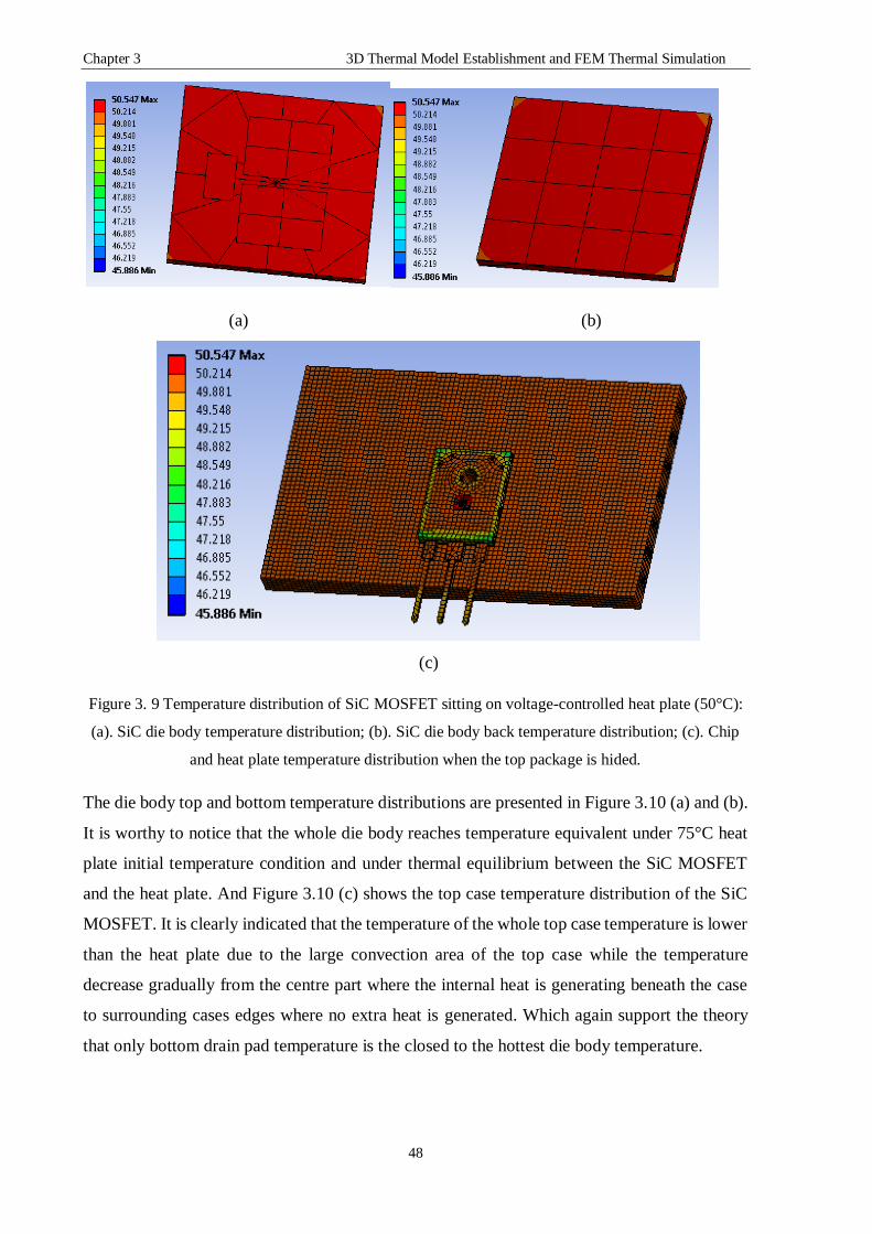
Chapter 3 3D Thermal Model Establishment and FEM Thermal Simulation
48
(a) (b)
(c)
Figure 3. 9 Temperature distribution of SiC MOSFET sitting on voltage-controlled heat plate (50°C):
(a). SiC die body temperature distribution; (b). SiC die body back temperature distribution; (c). Chip
and heat plate temperature distribution when the top package is hided.
The die body top and bottom temperature distributions are presented in Figure 3.10 (a) and (b).
It is worthy to notice that the whole die body reaches temperature equivalent under 75°C heat
plate initial temperature condition and under thermal equilibrium between the SiC MOSFET
and the heat plate. And Figure 3.10 (c) shows the top case temperature distribution of the SiC
MOSFET. It is clearly indicated that the temperature of the whole top case temperature is lower
than the heat plate due to the large convection area of the top case while the temperature
decrease gradually from the centre part where the internal heat is generating beneath the case
to surrounding cases edges where no extra heat is generated. Which again support the theory
that only bottom drain pad temperature is the closed to the hottest die body temperature.
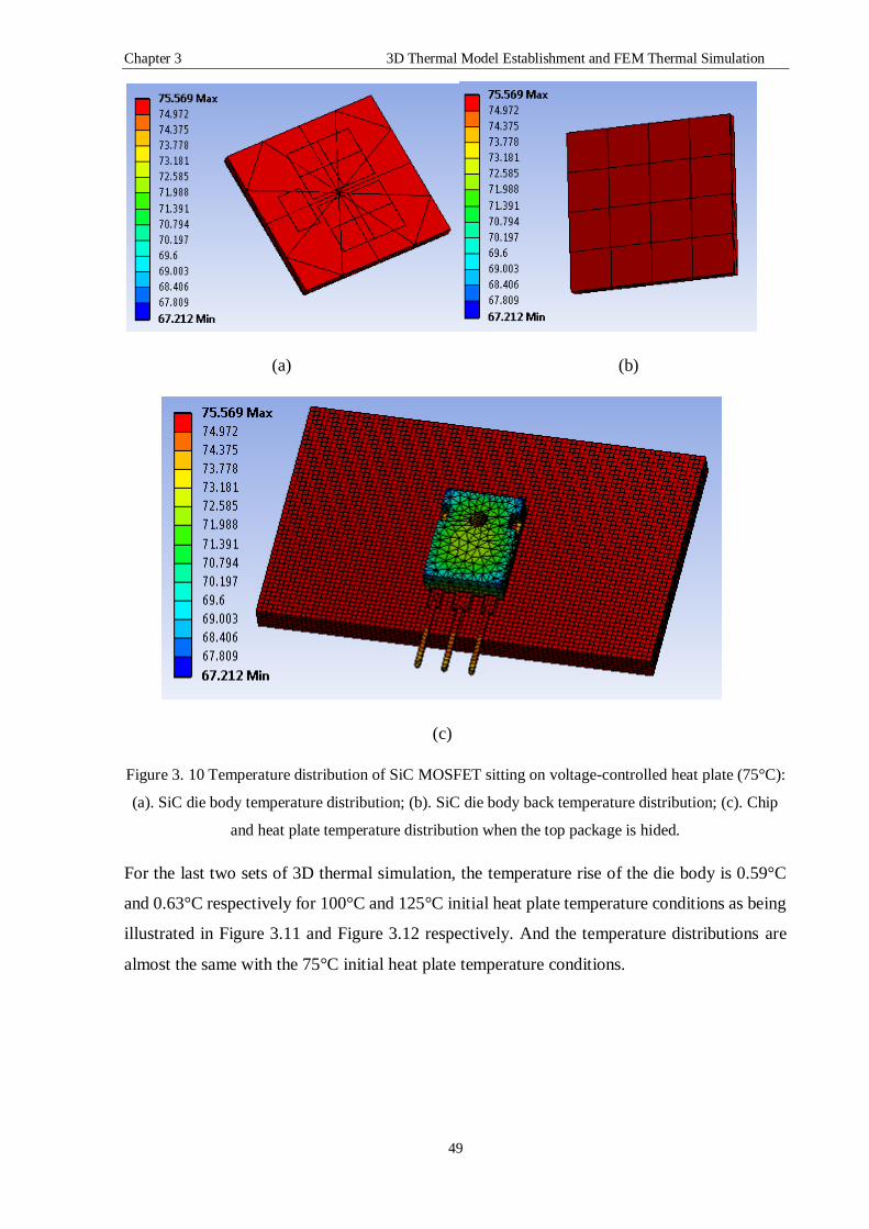
Chapter 3 3D Thermal Model Establishment and FEM Thermal Simulation
49
(a) (b)
(c)
Figure 3. 10 Temperature distribution of SiC MOSFET sitting on voltage-controlled heat plate (75°C):
(a). SiC die body temperature distribution; (b). SiC die body back temperature distribution; (c). Chip
and heat plate temperature distribution when the top package is hided.
For the last two sets of 3D thermal simulation, the temperature rise of the die body is 0.59°C
and 0.63°C respectively for 100°C and 125°C initial heat plate temperature conditions as being
illustrated in Figure 3.11 and Figure 3.12 respectively. And the temperature distributions are
almost the same with the 75°C initial heat plate temperature conditions.

Chapter 3 3D Thermal Model Establishment and FEM Thermal Simulation
50
(a) (b)
(c)
Figure 3. 11 Temperature distribution of SiC MOSFET sitting on voltage-controlled heat plate
(100°C): (a). SiC die body temperature distribution; (b). SiC die body back temperature distribution;
(c). Chip and heat plate temperature distribution when the top package is hided.
(a) (b)

Chapter 3 3D Thermal Model Establishment and FEM Thermal Simulation
51
(c)
Figure 3. 12 Temperature distribution of SiC MOSFET sitting on voltage-controlled heat plate
(125°C): (a). SiC die body temperature distribution; (b). SiC die body back temperature distribution;
(c). Chip and heat plate temperature distribution when the top package is hided.
3.4 Conclusion
In this chapter, a 3D model of the Cree/Wolfspeed C2M0080120D has been established using
Autodesk Inventor 3D software. The 3D model is produced based on the SiC MOSFET
datasheet and instructions of the TO-247-3 packaging. The established 3D model is then
imported into ANSYS finite element analysis software where corresponding materials of each
components of the SiC MOSFET are assigned accordingly. To emulate the die body power
losses generated during its operation, internal heat loss model is established in the simulation
and the amount of power losses are determined to distinguish different temperature rise under
various initial temperature conditions. It is determined that the bottom drain pad is the most
suitable position to measure the case temperature and the real Tj can be derived by adding the
die body temperature rise produced by its power losses. Further investigations will be carried
over in later experiment chapter.
Chapter 4 Small signal modelling of SiC MOSFETs
52
Chapter 4: Small signal modelling of SiC MOSFETs
In the beginning of this chapter, traditional TSEPs for Si devices have been simulated to
examine whether these methods can be applied to SiC MOSFET which turns out to be not a
way out for SiC MOSFET. Under this circumstance, it is crucial to propose new method to
precisely estimate Tj of SiC MOSFET. Following the simulation results, a small AC signal
injection method is proposed, and corresponding equivalent circuit is presented. The proposed
equivalent circuit is also verified via experimental test.
4.1 TSEP simulation in the SiC MOSFET
Traditional TESPs applied to Si devices have been proven not quite suitable for SiC power
devices. The main reason why traditional TSEPs fail to produce good results is that SiC is a
material that is less temperature-dependent and has a lower reverse recovery peak current and
a much faster rates of current and voltage change during the turn-on and turn-off process. Figure
4.1.1 shows results highlighting some differences in the behaviour of electrical parameters
during Tj changing in Si and SiC devices [15]. Figure 4.1.1 (a), shows the normalized RDS(on)
for the SiC MOSFET, Si MOSFET and COOLMOS. Both the Si MOSFET and COOLMOS
show good linearity, with a temperature resolution of around 1 mΩ/°C which is a reasonable
value as a TSEP [82]. However, the normalized RDS(on) of the 1st generation SiC MOSFETs is
not linear and has opposite temperature changing direction depending on the Tj value. Here,
when the value of Tj is lower than around 75 °C the normalized RDS(on) presents negative Tj
dependency, but when Tj becomes greater than 75 °C the normalized RDS(on) becomes positively
dependent on Tj. Furthermore, the 2nd generation of SiC MOSFETs, which is the latest
technology, show unified Tj dependency, but the even lower sensitivity makes it hard to be
utilized like in case of Si MOSFET. Clearly, as summarized, the RDS(on) is not applicable for
implementation as a TSEP for SiC MOSFETs. The diode technology for both Si and SiC
materials are also compared in Figures 4.1.1(b) and (c), showing the difference in the turn-off
process of a Si PIN diode and a SiC Schottky diode [15]. In case of the Si PiN diode, the reverse
recovery current peak (IPEAK) and reverse recovery current slope (dI/dt) increase along with
increments of in Tj. Both parameters can be measured and used as indicators of Tj. However,
for the SiC Schottky diode there is no visible change in IPEAK and dI/dt at different values of Tj
[15]. Figures 4.1.1 (d) and (e) show the gate voltage during turn-off transient for Si IGBTs and
SiC MOSFETs respectively. The turn-off time of the Si IGBT increases linearly with rising Tj;

Chapter 4 Small signal modelling of SiC MOSFETs
53
however, the turn-off time of the SiC MOSFET doesn’t present the same characteristic. Instead,
the turn-off time does not change linearly with increasing Tj [15].
Figure 4. 1(a) Dependency of n-state resistance on temperature for different MOSFET technologies;
(b) silicon PiN diode reverse recovery characteristics at different temperatures; (c) SiC Schottky diode
turn-off characteristics at different temperatures; (d) silicon IGBT gate voltage during turn-off at
different temperatures; (e) SiC MOSET gate voltage during turn-off at different temperatures [15].
These aforementioned comparisons between Si and SiC MOSFETs indicate that the traditional
TSEPs which can be utilised to extract the Tj of Si power electronic devices can hardly be
applied to the SiC MOSFET. In cases where the power device is a discrete SiC MOSFET, it is
also not viable to embed temperature sensors due to the small die-area and packaging limitations.
Also, the use of an infrared camera to extract values of SiC MOSFET Tj in online applications
is not feasible. However, the value of Tj of power electronic devices is one of the most crucial
parameters that indicates potential wear-out failures such as bond wire lift-off or solder fatigue.
For this reason, alternative solutions should be developed in order to precisely measure Tj in
discrete SiC MOSFETs during operation. In order to further investigate the behaviours of
different TSEPs for the discrete SiC MOSFET, double pulse test (DPT) simulations have been
established using LTspice simulation software. Specifically, in this research, the Cree 2rd
generation discrete SiC MOSFET (part number: C2M0080120D) is used. The analytical model
is provided by Cree [83] and is used in the simulations. As shown in Figure 4.2, a DPT test
circuit is presented. The basic rule for the double pulse test is to generate two different
successive gate pulses in the device to turn it on and off and to use appropriate probes and an
oscilloscope to capture the relevant current and voltage waveforms so as to analyse the
behaviour of the switch itself in both electrical and thermal terms. In this particular set-up,

Chapter 4 Small signal modelling of SiC MOSFETs
54
terminals Tj and Tc are specifically included in the design to analyse the self-heating of the
device as a function of time. The terminal Tc represents the case temperature and Tj represents
the junction temperature. The temperature connections are working as voltage pins. Therefore,
a potential difference of 1 V refers to a temperature difference of 1 °C.
The voltage at the Tj node contains information about the time-dependent Tj which in turn acts
directly on the temperature-dependent electrical model.
The Tc terminal has to be connected to either a voltage source (which denotes the ambient case
temperature) or to an external RC network (heat sink model) to observe its effect on Tj.
Figure 4. 2 DPT test based on Cree C2M0080120D discrete MOSFET.
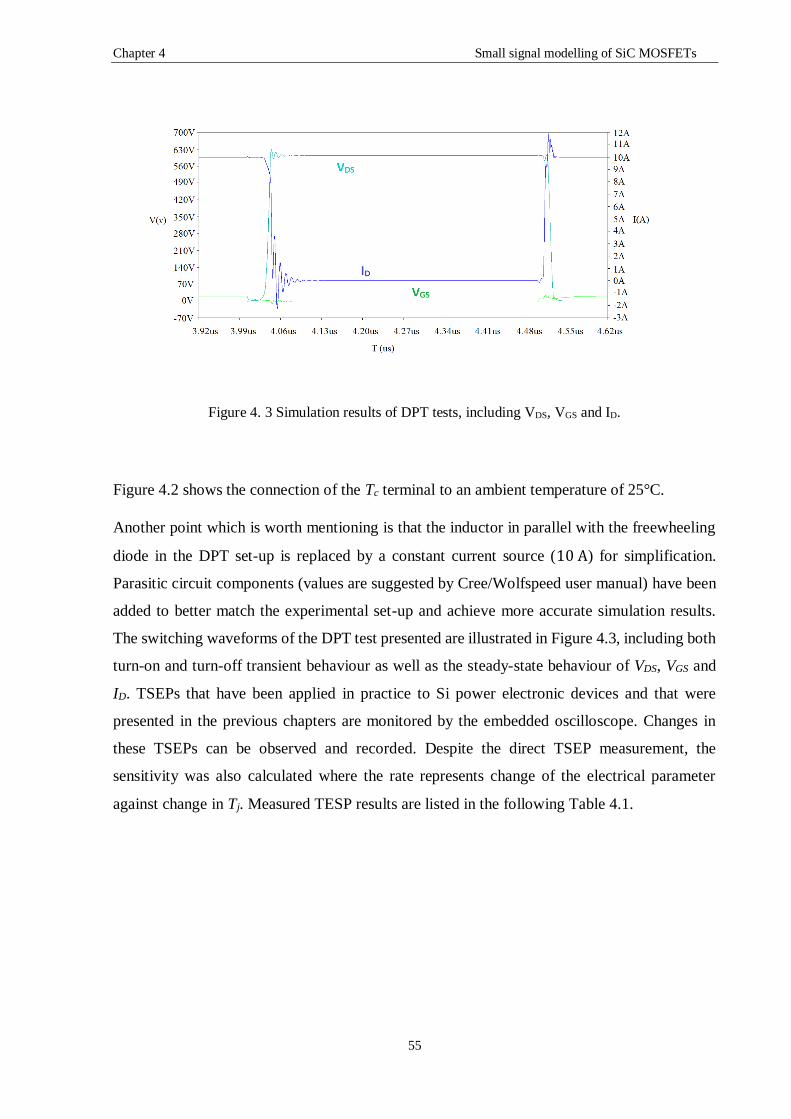
Chapter 4 Small signal modelling of SiC MOSFETs
55
Figure 4. 3 Simulation results of DPT tests, including VDS, VGS and ID.
Figure 4.2 shows the connection of the Tc terminal to an ambient temperature of 25°C.
Another point which is worth mentioning is that the inductor in parallel with the freewheeling
diode in the DPT set-up is replaced by a constant current source (10 A) for simplification.
Parasitic circuit components (values are suggested by Cree/Wolfspeed user manual) have been
added to better match the experimental set-up and achieve more accurate simulation results.
The switching waveforms of the DPT test presented are illustrated in Figure 4.3, including both
turn-on and turn-off transient behaviour as well as the steady-state behaviour of VDS, VGS and
ID. TSEPs that have been applied in practice to Si power electronic devices and that were
presented in the previous chapters are monitored by the embedded oscilloscope. Changes in
these TSEPs can be observed and recorded. Despite the direct TSEP measurement, the
sensitivity was also calculated where the rate represents change of the electrical parameter
against change in Tj. Measured TESP results are listed in the following Table 4.1.

Chapter 4 Small signal modelling of SiC MOSFETs
56
Table 4.1 Measured data of various TSEPs and calculated sensitivity values
The inherent parameters of the SiC MOSFET are either not linearly temperature-dependent or
the sensitivity levels of the parameters are low compared to Si power electronic devices, which
causes difficulties for current measurement technologies [4]. Therefor a new method for the
determination of Tj must be found. In the next section of this chapter, a new method is proposed.
4.2 Introduction of small signal AC analysis in power electronics
The general definition of small signal AC analysis can involves the superimposition of small
sinusoidal terminal currents and voltages upon an established steady-state (DC) device bias to
discover the device’s small signal AC characterization [84]. Here, small means that a tiny
amplitude of the injection signal will be limited so as to generate no harmonics within the device.
The relationship between the superimposed current and voltage will be characterized as a
function of frequency. On the other hand, large-signal AC behaviour, including harmonics
generation, is beyond the scope of this work, although the effects of harmonics generation
within the device can often be estimated by a parametric study of small-signal AC behaviour
versus DC bias [84].
Temperature (°C) 25 50 75
Sensitivity rate from
25 °C to 75 °C
Vth (V) 3.209 3.201 3.190 −0.38 mV/°C
Leak current(μA) 7.36 9.82 23.42 0.32 µA /°C
Miller plateau width (ns) 152.29 153.84 155.24 0.059 ns/°C
td(on) (ns) 31.05 30.31 29.72 −0.026 ns/°C
td(off) (ns) 126.76 127.97 129.05 0.0458 ns/°C
Vds slope delay time (ns) 6.05 5.98 5.91 −0.028 ns/°C
Ipeak (A) 10.6574 10.6563 10.6556 −3.6e − 4 A/°C

Chapter 4 Small signal modelling of SiC MOSFETs
57
Small-signal ac device analysis gives the possibilities to investigate useful device
characteristics like voltage gain AV, current gain AI as well as estimating the stability and noise
behaviour. The information collected from ac analysis can be critically useful to gain circuit-
level descriptions of device behaviour.
During the progress of this research and in the literature review, it can be found that small AC
signal analysis has been widely implemented in aspects of power electronic such as power
converter impedance detection and system identification [85-87].A method of impedance
measurement has been introduced for three-phase AC systems [84]. All impedance information
can be determined by injecting an unbalanced line-to-line current between two lines of the AC
system. Another example shows how a small-signal is injected into the inductor of a current-
controlled boost converter to determine the online inductor resistance [87]. So far, small signal
analysis has been applied to determine the resistance of the inductor, except where the technique
has been used to realize the optimisation of the controller [86]. These inspiring studies invoke
the possibility of the use of small AC signal analysis to investigate impedance change induced
by Tj based on the fact that the internal gate resistance Rint in the gate-source loop of the SiC
MOSFET is Tj dependent. If the value of Rint can be precisely estimated via small AC signal
analysis then the corresponding value of Tj can be extracted [88]. Under these circumstances, a
new method based on small AC signal analysis is proposed in this work.
In the present study, small signal analysis is applied to a single power electronics device to
determine. In this chapter, the equivalent parasitic circuit of the Cree SiC MOSFET in TO-247-
3 housing is derived and verified in order to utilize small signal analysis to estimate the
impedance loop change induced by the variation in Tj. In the following sections, small signal
models of SiC MOSFET are established and presented in order to further implement small AC
signal analysis and to investigate the influence of Tj on it. This is crucial in implementing
condition monitoring and to understand the parasitic loops so as to extracting the relevant
information.
4.3 Small AC signal modelling of the SiC MOSFET
In this section, a typical small signal model of the dynamic switching of an inductive load is
presented in order to explain how the small signal model can be used to extract individual
impedance parameters. Then the on-state and off-state small AC signal models are compared
to select the better one to be implemented in detail and to be used as the model to estimate the
Tj of the SiC MOSFET.

Chapter 4 Small signal modelling of SiC MOSFETs
58
As shown in Figure 4.4, a typical inductive switching small signal model is investigated to
explain how the small AC signal analysis works. The gate-source switching loop is forced
because the parameter that needs to be estimated is Rint.
Gate Driver
Cgd
Cgs
Cds DC
LinkRext Lg Rint
Ls
LdFWD
Lload
iD
iG
Drain-source Switching Loop
Gate-Source Switching LoopVGG
VGS
Figure 4. 4 Typical switching loop of an inductive load circuit.
During the switching transient of the SiC MOSFET, the gate-source voltage can be described
as in equation 4.1:
𝑉𝐺𝑆 = 𝑉𝐺𝐺 − 𝑅𝐺𝑖𝐺 − 𝐿𝐺𝑑𝑖𝐺
𝑑𝑡− 𝐿𝑆
𝑑(𝑖𝐺+𝑖𝐷)
𝑑𝑡 (4.1)
where VGS is the gate-source voltage, VGG is the gate driver output voltage, RG is the sum of Rext
and Rint, iG is the gate current, iD is the drain current and LG and LS are gate string inductance
and source string inductance respectively.
According to equation 4.1, during the transient and on-state of the SiC MOSFET, the variation
in VGS will induce a change of the value of iD [12]. In the case of a small signal injection, VGS is
superimposed with a small chirp signal which changes the output iD although this scenario
should be avoided in the normal operation of power devices. The values of diG/dt and diD/dt are
also Tj-dependent which makes it hard to pick up only the change in Rint. Then the small AC
signal model is narrowed down to the off state, which is established and investigated compared
in the following sections.

Chapter 4 Small signal modelling of SiC MOSFETs
59
4.4 Off-state small AC signal equivalent circuit modelling of the SiC MOSFET
An unbiased off-state small AC signal equivalent circuit is established and analysed in this
section, and the model is used to simulate the frequency response which is also compared later
with the results of impedance analyser.
Figure 4.5 illustrates an unbiased off-state small signal parasitic equivalent circuit for a Cree
second generation discrete SiC MOSFET (C2M0080120D) packaged in TO-247-3 housing.
Gate LeadsGate Bonding Wire
CGSSource Bonding Wires
Source Leads
RGx
CGD
CDS
Packaging ParasiticGate Drive SiC MOSFET Parasitic
RGIRGL
RSL LSL
LGL RGB
RSB LSB
LGB
Sign
al e
nera
tor
Figure 4. 5 Off-state equivalent circuit of a SiC MOSFET.
To analyse the effect of the influence of a change in Tj upon the internal gate resistance of the
SiC MOSFET, not only are the chip parasitic included in the equivalent circuit but also the
packaging parasitic and gate driver side parameters are presented. The values of parasitic
capacitances are calculated according to the relationships between input capacitor Ciss, output
capacitor Coss and reverse recovery capacitor Crss, as shown as equations 4.2, 4.3 and 4.4:
𝐶𝑖𝑠𝑠 = 𝐶𝐺𝐷 + 𝐶𝐺𝑆 (4.2)
𝐶𝑜𝑠𝑠 = 𝐶𝐺𝐷 + 𝐶𝐷𝑆 (4.3)
𝐶𝑟𝑠𝑠 = 𝐶𝐺𝐷 (4.4)
Here the values of Ciss, Coss, Crss are obtained from the datasheet provided by Cree, as shown in
Figure 4.6.

Chapter 4 Small signal modelling of SiC MOSFETs
60
Figure 4. 6 Typical parasitic capacitance VS VDS for C2M0080120D [83].
It is worth noting that these parasitic capacitances are voltage-dependent and thus the values
are extracted at the instance in which the drain-source voltage is equal to the DC link voltage.
During the unbiased test, the capacitance value is estimated as the drain-source voltage equal
to 0 V to emulate the unbiased condition. Then, during the biased test, the drain-source voltage
is set to be 600 V and the parasitic capacitors are accordingly: CGD=6.5 pF, CDS =73.5 pF, CGS
=943.5 pF. The individual package component value is calculated based on the diameter of the
TO-247-3 housing provided for the Cree SiC MOSFET (C2M0080120D) in its data sheet [83].
4.5 Parametric calculation of individual parasitic for MOSFET
4.5.1 Nominal values calculation of parasitic of SiC MOSFET
In the off-state equivalent parasitic loop, the only temperature-dependent component is the gate
internal resistance, and as stated in the literature review the temperature sensitivity of the
internal gate resistance is 1 mΩ/C° to 2 mΩ C° [88, 89].
Then, the values of parasitic parameters should be derived in order to be simulated later. The
device under study is in a TO-247 package. According to Cree, the standard for the sources
bond wire of TO-247 and TO-220 are either 4 15 mil diameter bond wires in parallel or 3
20 mil diameter bond wires in parallel. In this thesis, all the simulation results are based on 4
bond wires in parallel. The bond wire is made of aluminium.

Chapter 4 Small signal modelling of SiC MOSFETs
61
a. Calculation of bond wire resistance
The DC resistance of a conductor is calculated according to equation 4.5:
𝑅𝑑𝑐 =𝜌𝑙
𝐴 (4.5)
where 𝜌 is the resistivity of the material in Ω ∗ mm, l is its length in metres and A is the cross -
sectional area in square millimetre.
By checking the size of the bond wire in the TO-247, the length of the bond wire is usually 7
mm and the diameter as mentioned before is 15 mil, and the resistivity of aluminium is
2.6548 ∗ 10 −11Ω ∗ mm.
Thus, one single bond wire’s DC resistance can be calculated as 16.8 uΩ.
When there are 4 bond wires in parallel, the total resistance can be calculated as 4.2 uΩ.
The AC resistance of a round straight wire is calculated according to equation 4.6:
𝑅𝑎𝑐 =𝜌𝑥𝑙
𝐴𝑒𝑓𝑓 (4.6)
Where ρ is the resistivity of the conductor in Ω ∗ m, l is the Length of the conductor in mm and
Aeff is the effective cross-sectional area used in mm.
Equation 4.7 below represents the skin surface effect:
𝛿 = √𝜌
𝜋𝑓𝜇 (4.7)
Where ρ is the resistivity of the conductor in Ω ∗ m, f is the frequency in Hertz, and μ is the
absolute magnetic permeability of the conductor.
The absolute magnetic permeability is (μ) = μo x μr
where μo = 4π x 10−7 H/m
The Aeff can thus be expressed as equation 4.8:
𝐴𝑒𝑓𝑓 = 𝛿𝜋𝑑 (4.8)
Where d is the diameter of the conductor.
This means that the cross-sectional area used is too large from high frequencies down to the
point where the skin depth becomes about half of the radius of the conductor, at which point

Chapter 4 Small signal modelling of SiC MOSFETs
62
the inaccuracies increase and eventually the calculated area used becomes bigger than the actual
conductor. Therefore, the calculation method is only an approximation and is then only usable
when r >> δ, where in the case of bond wire it matches such a scenario.
As a result, the AC resistance at different frequencies could be calculated. For a frequency of
40 MHz, the AC resistance of a single wire is 12.6 mΩ.
When 4 bond wires sit in parallel, the total resistance is 3.15 mΩ.
Bond wire resistances with different numbers of bond wire lift-offs can be derived accordingly.
b. Calculation of bond wire inductance
For the calculation of the bond wire inductance, the following approximated equation 4.10 is
used:
𝐿 =𝜇0
2𝛱∗ 𝑙 [𝑙𝑛 (
𝑙
𝑟+ √1 +
𝑙2
𝑟2) − √1 +𝑙2
𝑟2 +𝑟
𝑙+
1
4] (4.10)
where r is the bond wire radius, l is its length and 𝜇0 is the permeability of free space.
(1.2566e−6 H/m)
For l>>r, a simplification can be derived from the above as in equation 4.11:
𝐿 =𝜇0
2𝛱∗ 𝑙 [𝑙𝑛 (
2𝑙
𝑟) − 0.75] (4.11)
In this case, the length of the bond wire is 7 mm and the radius of the bond wire is 187.5 um.
As a result, the single bond wire inductance is calculated as 5 nH, and accordingly the total
inductance can be derived based on the number of bond wires in parallel.
c. Calculation of lead resistance and inductance
Similarly, based on the normal lead size of TO-247 package, the resistances and inductances of
both gate lead and source lead can be calculated using the aforementioned equations and
formulae. The results are shown below.
The typical gate lead resistance is about 14.6 mΩ, which is equal to the source resistance and
the inductance is calculated as 15 nH.
In summary, the individual parasitic values of each component appearing in the equivalent
circuit are listed in the following Table 4.2.

Chapter 4 Small signal modelling of SiC MOSFETs
63
Table 4. 2 Results of small AC signal equivalent circuit parameters calculation
External gate resistance 10 Ω
Lead resistance 14.6 mΩ
Lead inductance 6 nH
Internal gate resistance 4.6 Ω @25 °C [83]
Gate source capacitance 1263 pF @25 °C [83]
Single bond wire resistance 12.6 mΩ
Single bond wire inductance 5 nH
4.5.2 Parasitic parameters of SiC MOSFET when considering temperature influence.
Among all those parameters calculated in section 4.5.1, gate-source capacitance is temperature
invariant, inductances including lead inductance and bond wire inductance are also not
changing against temperature. The only temperature dependent parasitic is resistors. In this
section, all the resistance listed in the Table 4.2 will be calibrated against Tj. Consider the
material of external resistor and lead are pure copper, it consists of 99% copper in datasheet, to
simplify calculation and the temperature coefficient of copper is 0.393% per degree C (3.93×10-
3/°C) at 20°C. And the bond wire is pure aluminium and the temperature coefficient of
aluminium is 4.308×10⁻³/°C at 20°C.
The generic formula of temperature effects on resistance is as follow:
𝑅 = 𝑅𝑟𝑒𝑓 × [1 + 𝛼(𝑇𝑗 − 𝑇𝑟𝑒𝑓) (4.1)
Where R is the conductor resistance at temperature Tj, Rref is the conductor resistance at
reference temperature Tref, which is usually 20°C, α is the temperature coefficient of resistance
of the conductor material, Tj is the conductor temperature in degrees Celsius and Tref is the
reference temperature that α is specified at for the conductor material. The temperature
dependent of external gate resistance, lead resistance and bond wire resistance can be calculated

Chapter 4 Small signal modelling of SiC MOSFETs
64
using equation 4.1 by assigning all parameters needed. The results are summarized in table 4.3
below:
Table 4. 3 Temperature dependent resistances of parasitic in SiC MOSFET
Parameter Nominal 25°C 50°C 75°C 100°C 125°C
External gate resistor (Ω) 10 10.20 11.18 12.16 13.14 14.13
Lead resistance (mΩ) 14.6 14.89 16.32 17.75 19.18 20.63
Bond wire resistance (mΩ) 12.6 12.85 14.09 15.32 16.56 17.80
Although the external gate resistance values are listed, the external gate resistor will remain
10Ω in the simulation since it is at the gate driver side and the ambient temperature will be
much lower than the Tj of the SiC MOSFET. For lead resistance and bond wire resistance, the
value of resistance at each test temperature will be imported into the simulation software to
minimize the simulation error.
4.6 Verification of small ac signal equivalent circuit
The first step in testing the equivalent circuit is to use simulation software to examine its
behaviour. In this research, LTspice [90] software is used to fully simulate the operation of the
small AC signal equivalent circuit. At the very beginning, an unbiased off-state circuit is
simulated, and the simulation schematic is shown in Figure 4.7.
Figure 4. 7 Schematic of un-biased off-state gate-source equivalent circuit for SiC MOSFET.
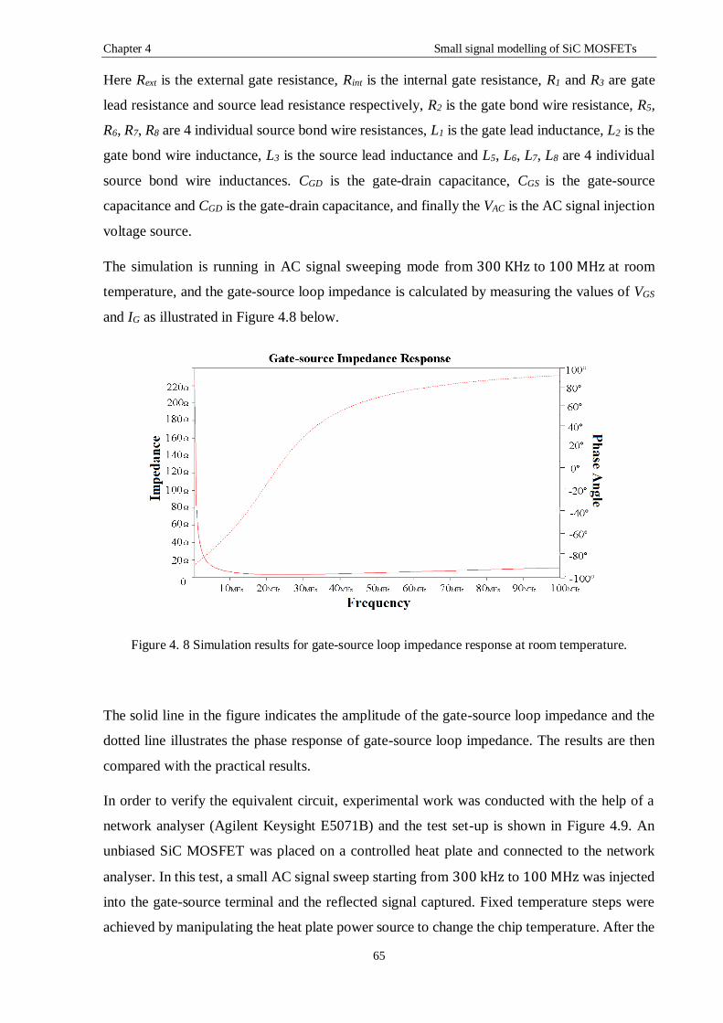
Chapter 4 Small signal modelling of SiC MOSFETs
65
Here Rext is the external gate resistance, Rint is the internal gate resistance, R1 and R3 are gate
lead resistance and source lead resistance respectively, R2 is the gate bond wire resistance, R5,
R6, R7, R8 are 4 individual source bond wire resistances, L1 is the gate lead inductance, L2 is the
gate bond wire inductance, L3 is the source lead inductance and L5, L6, L7, L8 are 4 individual
source bond wire inductances. CGD is the gate-drain capacitance, CGS is the gate-source
capacitance and CGD is the gate-drain capacitance, and finally the VAC is the AC signal injection
voltage source.
The simulation is running in AC signal sweeping mode from 300 KHz to 100 MHz at room
temperature, and the gate-source loop impedance is calculated by measuring the values of VGS
and IG as illustrated in Figure 4.8 below.
Figure 4. 8 Simulation results for gate-source loop impedance response at room temperature.
The solid line in the figure indicates the amplitude of the gate-source loop impedance and the
dotted line illustrates the phase response of gate-source loop impedance. The results are then
compared with the practical results.
In order to verify the equivalent circuit, experimental work was conducted with the help of a
network analyser (Agilent Keysight E5071B) and the test set-up is shown in Figure 4.9. An
unbiased SiC MOSFET was placed on a controlled heat plate and connected to the network
analyser. In this test, a small AC signal sweep starting from 300 kHz to 100 MHz was injected
into the gate-source terminal and the reflected signal captured. Fixed temperature steps were
achieved by manipulating the heat plate power source to change the chip temperature. After the

Chapter 4 Small signal modelling of SiC MOSFETs
66
capture of the reflected signals, data was processed in MATLAB to generate the corresponding
impedance frequency response for various temperatures.
(a) (b)
Figure 4. 9 Experiment set-ups: (a) Agilent Keysight E5071B Network analyzer;
(b) temperature-controlled heat plate.
The same small signal analysis was carried out with the data generated from experiments.
Figures 4.10(a) and 4.10(b) show the simulated and measured data for impedance magnitude
and phase respectively. Both figures represent results at one chip temperature and simulation
and experimental results are in close proximity.
(a) (b)
Figure 4. 10 Simulation results and network analyser results: (a) impedance magnitude at T=25oC; (b)
impedance phase at T=25oC.
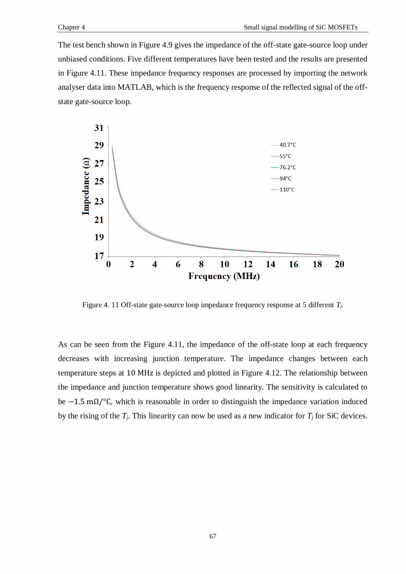
Chapter 4 Small signal modelling of SiC MOSFETs
67
The test bench shown in Figure 4.9 gives the impedance of the off-state gate-source loop under
unbiased conditions. Five different temperatures have been tested and the results are presented
in Figure 4.11. These impedance frequency responses are processed by importing the network
analyser data into MATLAB, which is the frequency response of the reflected signal of the off-
state gate-source loop.
Figure 4. 11 Off-state gate-source loop impedance frequency response at 5 different Tj.
As can be seen from the Figure 4.11, the impedance of the off-state loop at each frequency
decreases with increasing junction temperature. The impedance changes between each
temperature steps at 10 MHz is depicted and plotted in Figure 4.12. The relationship between
the impedance and junction temperature shows good linearity. The sensitivity is calculated to
be −1.5 mΩ/°C, which is reasonable in order to distinguish the impedance variation induced
by the rising of the Tj. This linearity can now be used as a new indicator for Tj for SiC devices.

Chapter 4 Small signal modelling of SiC MOSFETs
68
Figure 4. 12 Impedance VS Tj at 10 MHz.
In addition, the proposed method is investigated in SiC module as well to examine whether the
method can be extended to SiC module or not.
A single phase-leg SiC Module is used to conduct simulation to examine the proposed method.
As can be seen from Figure 1 that a single-phase half bridge inverter with a resistive load is
presented, the simulation is divided into two parts: the first part is assuming that when the top
MOSFET is at its off state (Figure 4.13(a))and then the small AC chirp signal is injected into
the gate-source terminal of the top switch and the bottom switch is constantly on, the second
part of the experiment is doing the opposite (Figure 4.13(b)). Finally, as a comparison set, a
discrete SiC MOSFET is simulated and small AC chirp signal is superimposed into the gate
terminal when the MOSFET is during its off state with a resistive load as demonstrated in Figure
4.13(c).
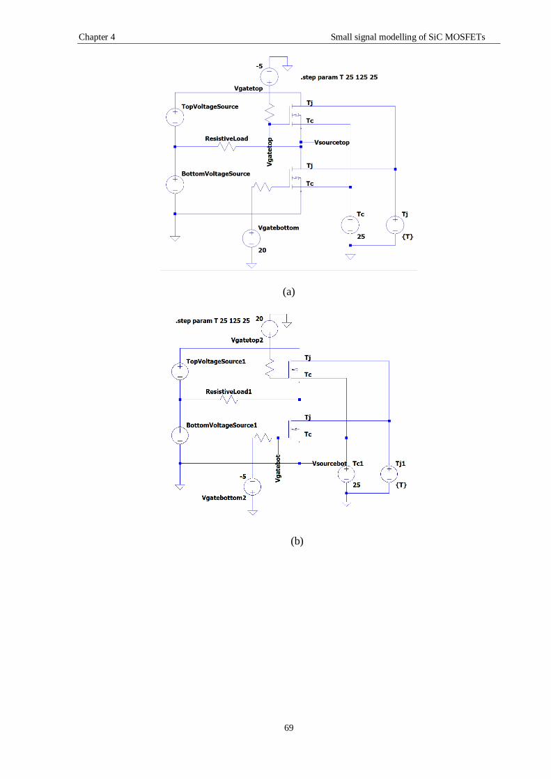
Chapter 4 Small signal modelling of SiC MOSFETs
69
(a)
(b)

Chapter 4 Small signal modelling of SiC MOSFETs
70
(c)
Figure 4. 13 LTspice Simulation Schematics: (a) Top switch is off and the small AC signal is
superimposed into the gate terminal of the SiC MOSFET while the bottom switch is at its on-stated;
(b) Top switch is at its on-stated while the small AC signal is superimposed into the gate terminal of
bottom switch; (c) Small AC chirp signal is superimposed into the gate terminal of a discrete SiC
MOSFET when it is completely off.
All the parameters used in simulation for all three simulating conditions are identical: those
parameters include supply voltage of all three DC voltage supply, maximum gate-source
voltage when the switch is on, minimum gate-source voltage when the switch is off, the
resistance of the resistive load, the case temperature of all three SiC MOSFETs. Those input
parameters are listed in Table 4.4 below.
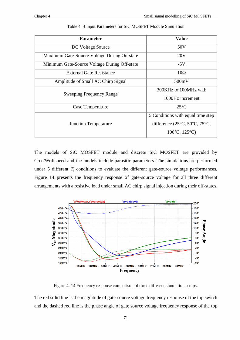
Chapter 4 Small signal modelling of SiC MOSFETs
71
Table 4. 4 Input Parameters for SiC MOSFET Module Simulation
Parameter Value
DC Voltage Source 50V
Maximum Gate-Source Voltage During On-state 20V
Minimum Gate-Source Voltage During Off-state -5V
External Gate Resistance 10Ω
Amplitude of Small AC Chirp Signal 500mV
Sweeping Frequency Range 300KHz to 100MHz with
1000Hz increment
Case Temperature 25°C
Junction Temperature
5 Conditions with equal time step
difference (25°C, 50°C, 75°C,
100°C, 125°C)
The models of SiC MOSFET module and discrete SiC MOSFET are provided by
Cree/Wolfspeed and the models include parasitic parameters. The simulations are performed
under 5 different Tj conditions to evaluate the different gate-source voltage performances.
Figure 14 presents the frequency response of gate-source voltage for all three different
arrangements with a resistive load under small AC chirp signal injection during their off-states.
Figure 4. 14 Frequency response comparison of three different simulation setups.
The red solid line is the magnitude of gate-source voltage frequency response of the top switch
and the dashed red line is the phase angle of gate source voltage frequency response of the top
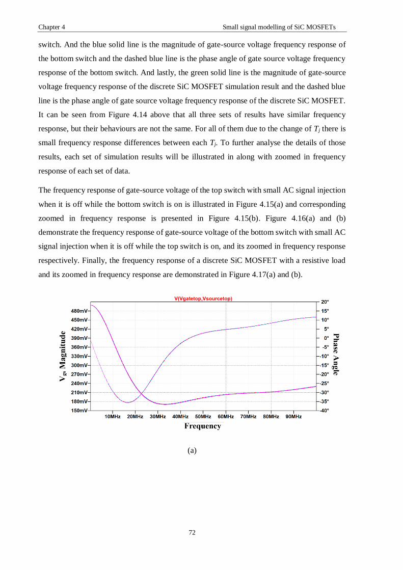
Chapter 4 Small signal modelling of SiC MOSFETs
72
switch. And the blue solid line is the magnitude of gate-source voltage frequency response of
the bottom switch and the dashed blue line is the phase angle of gate source voltage frequency
response of the bottom switch. And lastly, the green solid line is the magnitude of gate-source
voltage frequency response of the discrete SiC MOSFET simulation result and the dashed blue
line is the phase angle of gate source voltage frequency response of the discrete SiC MOSFET.
It can be seen from Figure 4.14 above that all three sets of results have similar frequency
response, but their behaviours are not the same. For all of them due to the change of Tj there is
small frequency response differences between each Tj. To further analyse the details of those
results, each set of simulation results will be illustrated in along with zoomed in frequency
response of each set of data.
The frequency response of gate-source voltage of the top switch with small AC signal injection
when it is off while the bottom switch is on is illustrated in Figure 4.15(a) and corresponding
zoomed in frequency response is presented in Figure 4.15(b). Figure 4.16(a) and (b)
demonstrate the frequency response of gate-source voltage of the bottom switch with small AC
signal injection when it is off while the top switch is on, and its zoomed in frequency response
respectively. Finally, the frequency response of a discrete SiC MOSFET with a resistive load
and its zoomed in frequency response are demonstrated in Figure 4.17(a) and (b).
(a)
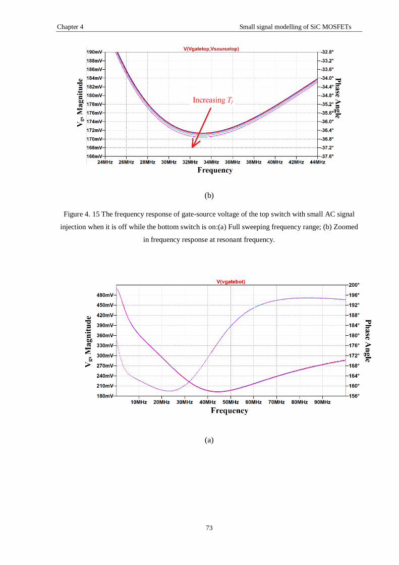
Chapter 4 Small signal modelling of SiC MOSFETs
73
(b)
Figure 4. 15 The frequency response of gate-source voltage of the top switch with small AC signal
injection when it is off while the bottom switch is on:(a) Full sweeping frequency range; (b) Zoomed
in frequency response at resonant frequency.
(a)
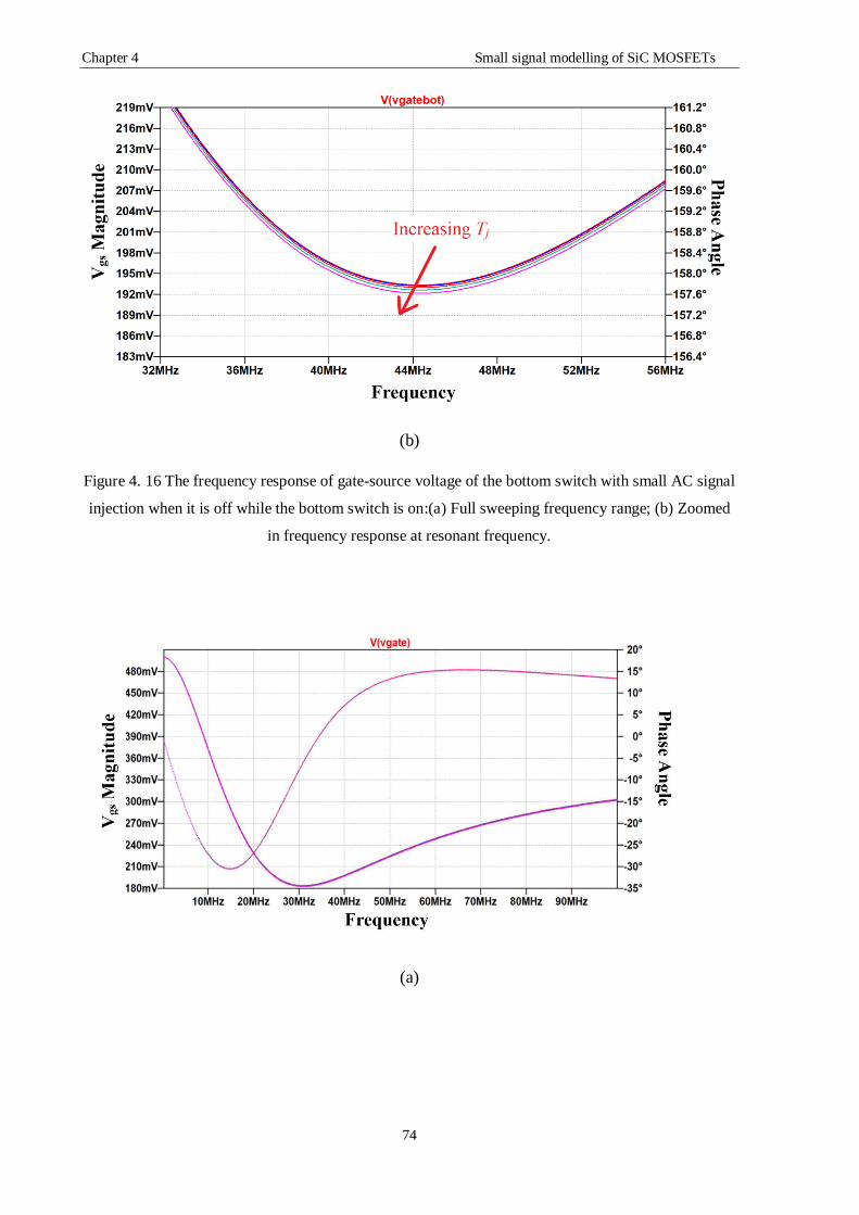
Chapter 4 Small signal modelling of SiC MOSFETs
74
(b)
Figure 4. 16 The frequency response of gate-source voltage of the bottom switch with small AC signal
injection when it is off while the bottom switch is on:(a) Full sweeping frequency range; (b) Zoomed
in frequency response at resonant frequency.
(a)

Chapter 4 Small signal modelling of SiC MOSFETs
75
Figure 4. 17 The frequency response of gate-source voltage of the single discrete SiC
MOSFET with small AC signal injection when it is off while the bottom switch is on:(a) Full
sweeping frequency range; (b) Zoomed in frequency response at resonant frequency.
It can be concluded from results illustrated above that under all three conditions, the magnitude
of the gate-source voltage frequency response exhibit a homogenous decreasing trend with the
increasing of the Tj. However, it is clearly indicated in those zoomed in frequency responses
that the resonant frequency where the gate-source loop presents the lowest impedance is
different. The results shown above means that the proposed small AC signal injection method
can be applied to SiC modules since the frequency response shows similar behaviour. But
individual calibration tests need to be carried out for each SiC MOSFET inside the module to
establish individual look-up table.

Chapter 4 Small signal modelling of SiC MOSFETs
76
4.7 Conclusion
In this chapter it has been concluded that the traditional TSEPs are difficult to apply to SiC
MOSFETs and an alternative method is proposed for detecting the Tj of SiC MOSFETs using
a small AC signal analysis technique. An unbiased SiC MOSFET is excited by injecting a high
frequency perturbation signal into the gate lead, and the frequency response is calculated using
a signal processing technique. Simulations and practical work were carried out. A precise small-
signal gate-source equivalent circuit was developed and used in simulations and the results
compared with practical results gained from a network analyser. The two sets of results exhibit
a good match. The temperature dependence of loop impedance was tested and captured using
the network analyser. It was found that, at a certain frequency, the impedance frequency
response shows good linearity and reasonable sensitivity which can be easily detected. The
results obtained have demonstrated the capability of the proposed technique. In the next chapter,
experimental results with fully biased test set-ups are demonstrated and discussed.
.

Chapter 5 Experimental Implementation Based on Small AC Signal Injection Technique
77
Chapter 5. Experimental Implementation Based on Small AC Signal
Injection Technique
In the previous chapter, the internal gate resistance (Rint) of a Cree C2M0080120D SiC
MOSFET is extracted with the help of a network analyser under unbiased conditions. However,
using such expensive equipment to extract thermal information is impractical in real
applications. Thus, an alternative solution needs to be developed. In this chapter, practical tests
are established using a function generator to generate a high frequency chirp signal. All the
experimental set-ups and results are presented including the high frequency chirp signal
injection circuit set-up, along with experimental results for the unbiased and biased signal
injection and finally the method is validated using a Cree/Wolfspeed SiC MOSFET evaluation
toolkit.
5.1 Gate source voltage dependency against temperature
To further examine the temperature dependency of the internal gate resistance and to establish
circuit which is in applicable practice instead of using a network analyser which is in principle
not suitable for online or in-situ monitoring, a gate-source voltage measurement test circuit is
proposed based on the equivalent circuit of the gate-source loop of the SiC MOSFET during
the off-state. Initially, an unbiased test is established to compare the results with those using the
network analyser and to verify the proposed theory. Then, after the verification, the SiC
MOSFET is tested under various DC bias conditions to determine the influences of different
DC biasing and corresponding gate-source voltage frequency responses in terms of the
relationship with changes in Tj.
5.1.1 Unbiased test
As mentioned in previous chapters, it is impractical to directly measure the device’s Tj of
devices packaged with TO housing. This study uses the small signal injection technique to find
the frequency response of the gate-source impedance loop during the off-state and to analyse
the variation in internal gate impedance induced by changes in Tj. Following the tests using the
network analyser described in Chapter 4, a small signal injection circuit is designed based on
the off-state equivalent parasitic circuit illustrated in Figure 5.1. As shown in Figure 5.1, the
SiC MOSFET is unbiased between drain and source. A Tektronix AFG3102 waveform
generator sweeps a chirp signal which frequencies varying from 300 kHz to 100 MHz with a

Chapter 5 Experimental Implementation Based on Small AC Signal Injection Technique
78
peak amplitude of 600 mV , although only the frequency range from 5 MHz to 10 MHz is
required. A Pico-scope 3206b for data acquisition is used. This device has a sampling rate of
100 Msps. Detailed introduction of this Pico-scope is organized in Appendix F. A 1.2 kV SiC
MOSFET from CREE/Wolfspeed with the reference number C2M0080120D has been placed
on a voltage-controlled heat plate and connected to the Pico-scope to capture the gate-source
voltage signal. The heat plate temperature was varied between to 100 °C under control of its
voltage source. Increments in temperature step of 20 °C were selected, which means that a total
of 5 temperature steps are used during the off-stated test. At each temperature step, the
temperature is measured by a thermal coupler and displayed by a thermometer. In order to
achieve thermal equilibrium and to make sure that the test is undertaken when the chip
temperature does not change, the gate-source voltage is captured 5 minutes after the
thermometer displays no further changes. After the chip temperature has stabilized, the
aforementioned chirp signal generated by the waveform generator is injected into the gate-
source terminals and the voltage between the gate terminal and the source terminal is captured
by the Pico-scope. The information acquired is directly saved to a PC to be processed afterwards.
A photograph of the unbiased small signal injection test set-up is presented in Figure 5.2.
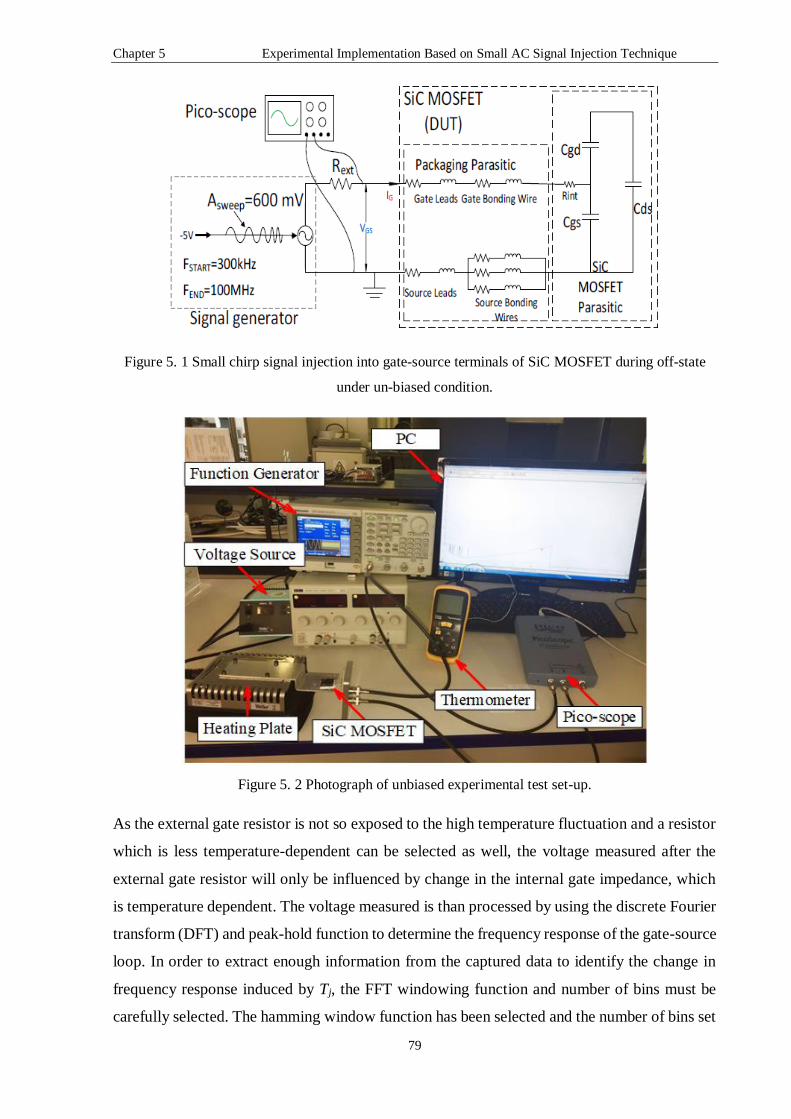
Chapter 5 Experimental Implementation Based on Small AC Signal Injection Technique
79
Figure 5. 1 Small chirp signal injection into gate-source terminals of SiC MOSFET during off-state
under un-biased condition.
Figure 5. 2 Photograph of unbiased experimental test set-up.
As the external gate resistor is not so exposed to the high temperature fluctuation and a resistor
which is less temperature-dependent can be selected as well, the voltage measured after the
external gate resistor will only be influenced by change in the internal gate impedance, which
is temperature dependent. The voltage measured is than processed by using the discrete Fourier
transform (DFT) and peak-hold function to determine the frequency response of the gate-source
loop. In order to extract enough information from the captured data to identify the change in
frequency response induced by Tj, the FFT windowing function and number of bins must be
carefully selected. The hamming window function has been selected and the number of bins set

Chapter 5 Experimental Implementation Based on Small AC Signal Injection Technique
80
to 1024, and 247 data points are captured in order to produce the frequency response of the VGS.
This selection is intended to achieve a balance between accuracy and the time taken to process
the data.
Figure 5.3(a) shows results of the magnitude frequency response for the gate-source loop at
different junction temperatures between 5 MHz and10 MHz. As illustrated in Figure 5.3(a),
change in values of amplitude is in a nearly linear fashion with the Tj over the full frequency
range; however, at single frequencies, the difference between the amplitudes is very small
(approximately−0.03 mV/°C). Furthermore, the linearity is not constant for each frequency
point.
In order to increase resolution, a new but simple method is proposed. Rather than presenting
one value of magnitude against its corresponding frequency over the frequency range, the
values of magnitude are integrated over the full frequency range for one junction temperature
point, as shown in equation (5.1).
𝑀𝑎𝑔𝑛𝑖𝑡𝑢𝑑𝑒𝑇𝑜𝑡𝑎𝑙 = ∑ 𝑀𝑎𝑔𝑛𝑖𝑡𝑢𝑑𝑒𝑠𝑎𝑚𝑝𝑙𝑒 𝑝𝑜𝑖𝑛𝑡 𝐹𝑒𝑛𝑑𝐹𝑠𝑡𝑎𝑟𝑡
(5.1)
where, MagnitudeTotal is the integrated magnitude of the VGSpeak over the whole frequency range,
Magnitudesample point is the magnitude of VGSpeak captured at each sampling data point and Fstart,
Fend represent the starting and ending frequencies respectively.
The accumulation of magnitude at each frequency consequently leads to a larger sensitivity
number which is more useful in practical applications. The accumulated magnitude at five
different Tj are presented which means that only five data points are presented where each data
point represents one temperature. Figure 5.3(b) shows results based on the data from Figure
5.3(a), where there are only 5 data points. The change in measured integrated magnitude of
VGSpeak is nearly linear with respect to temperature. However, a linearization fitting curve has
been added and is shown in Figure 5.3(b) too. The relationship between the integrated
magnitude of VGSpeak and temperature can be derived from the graph as follows:
𝑀𝑎𝑔𝑛𝑖𝑡𝑢𝑑𝑒𝑇𝑜𝑡𝑎𝑙 = −3.0227 × 𝑇𝑗 + 5854.6 (5.2)
where Tj is the junction temperature.
Figure 5. 3(b) shows a sensitivity of −3 mV/°C, which is 100 times greater compared to that
derived in the method described previously. In Chapter 4, the impedance frequency response
of the gate-source was −1.5 mΩ/°C (linearly) for the same SiC MOSFET. However, in the

Chapter 5 Experimental Implementation Based on Small AC Signal Injection Technique
81
verification test set-up in Chapter 4, an expensive network analyser was used. In this
experimental set-up, the magnitude frequency response of gate-source voltage is analysed, and
the results also present a nearly linear relationship with a good resolution factor of −3mV/°C.
However, the proposed technique only requires a standard frequency generator and a Pico-
scope, which reduces the hardware complexity and cost.

Chapter 5 Experimental Implementation Based on Small AC Signal Injection Technique
82
(a)
(b)
Figure 5. 3 Frequency response analysis: (a) Frequency response of magnitude of VGSpeak from 5 MHz
to 10 MHz; (b) integrated magnitude of VGSpeak.

Chapter 5 Experimental Implementation Based on Small AC Signal Injection Technique
83
In this section, a possible alternative to determine the junction temperature of SiC MOSFETs
is tested under unbiased conditions. High frequency voltage signals with low amplitude are
injected into an unbiased SiC MOSFET to excite the gate-source impedance. The voltage is
recorded and an FFT analysis is performed. All values of magnitude of VGSpeak for each
frequency are integrated over a frequency range from 5 MHz to 10 MHz at different
temperatures. It can be seen that the integrated amplitude shows a nearly linear dependence on
temperature with a sensitivity of −3mV/°C. The proposed solution requires little hardware and
costs much less compared to the previously described method proposed in Chapter 4, where a
network analyser was used to determine the Tj of the SiC MOSEFET. In the next section, the
biased tests performed under different DC biasing conditions are presented and discussed.
5.1.2 Biased test with chirp signal injection
a. Biased test with different DC bias voltages with chirp signal directly injected
After the unbiased test has been conducted and analysed, the next step to further extend the
experiment is to apply a DC bias voltage to the drain-source terminals of the SiC MOSFET. In
order to achieve such a test configuration, a 4-leg inverter designed at Newcastle University is
used (the schematic of the 4-leg inverter is presented in Appendix D). The schematic of the test
set-up is presented in Figure 5.4.
Figure 5. 4 Schematic of signal injection test under DC biased condition using a 4-leg inverter.
As shown in Figure 5.4, the SiC MOSFET is sitting in one phase leg and the drain terminal is
connected to node Vdc+ while the source terminal is connected to node V1. The Vdc+ and V1
nodes are also connected to a TopCon Quadro programmable DC power supply manufactured
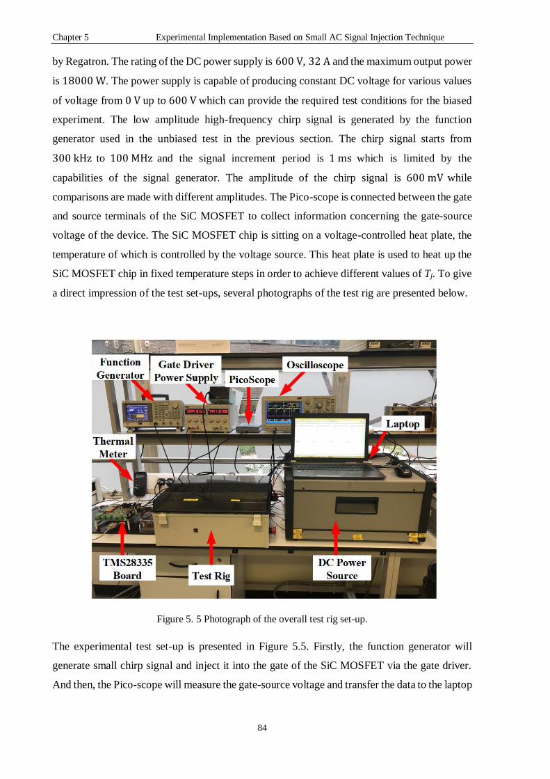
Chapter 5 Experimental Implementation Based on Small AC Signal Injection Technique
84
by Regatron. The rating of the DC power supply is 600 V, 32 A and the maximum output power
is 18000 W. The power supply is capable of producing constant DC voltage for various values
of voltage from 0 V up to 600 V which can provide the required test conditions for the biased
experiment. The low amplitude high-frequency chirp signal is generated by the function
generator used in the unbiased test in the previous section. The chirp signal starts from
300 kHz to 100 MHz and the signal increment period is 1 ms which is limited by the
capabilities of the signal generator. The amplitude of the chirp signal is 600 mV while
comparisons are made with different amplitudes. The Pico-scope is connected between the gate
and source terminals of the SiC MOSFET to collect information concerning the gate-source
voltage of the device. The SiC MOSFET chip is sitting on a voltage-controlled heat plate, the
temperature of which is controlled by the voltage source. This heat plate is used to heat up the
SiC MOSFET chip in fixed temperature steps in order to achieve different values of Tj. To give
a direct impression of the test set-ups, several photographs of the test rig are presented below.
Figure 5. 5 Photograph of the overall test rig set-up.
The experimental test set-up is presented in Figure 5.5. Firstly, the function generator will
generate small chirp signal and inject it into the gate of the SiC MOSFET via the gate driver.
And then, the Pico-scope will measure the gate-source voltage and transfer the data to the laptop
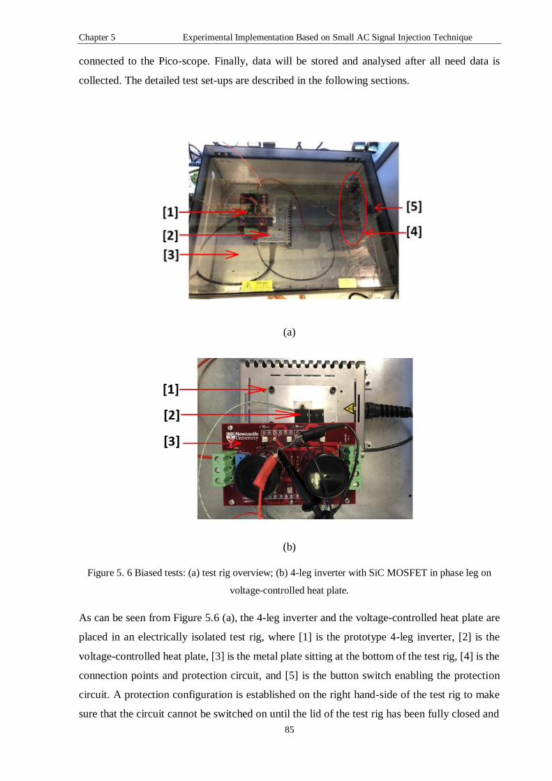
Chapter 5 Experimental Implementation Based on Small AC Signal Injection Technique
85
connected to the Pico-scope. Finally, data will be stored and analysed after all need data is
collected. The detailed test set-ups are described in the following sections.
(a)
(b)
Figure 5. 6 Biased tests: (a) test rig overview; (b) 4-leg inverter with SiC MOSFET in phase leg on
voltage-controlled heat plate.
As can be seen from Figure 5.6 (a), the 4-leg inverter and the voltage-controlled heat plate are
placed in an electrically isolated test rig, where [1] is the prototype 4-leg inverter, [2] is the
voltage-controlled heat plate, [3] is the metal plate sitting at the bottom of the test rig, [4] is the
connection points and protection circuit, and [5] is the button switch enabling the protection
circuit. A protection configuration is established on the right hand-side of the test rig to make
sure that the circuit cannot be switched on until the lid of the test rig has been fully closed and

Chapter 5 Experimental Implementation Based on Small AC Signal Injection Technique
86
the button switch connected to the interlock of the power supply is completely closed. Both the
4-leg inverter and the heat plate are firmly screwed onto a metal plate which is connected to the
earth. Figure 5.6 (b) specifically focuses on the 4-leg inverter, where [1] is the voltage-
controlled heat plate, [2] is the device under test (DUT) and [3] is the 4-leg inverter. As can be
seen from Figure 5.6 (b), the SiC MOSFET is firmly screwed onto the heat plate. There is a Si
sheet sitting between the SiC MOSFET and the heat plate to establish electrical isolation
between them since the SiC MOSFET is a non-isolated type.
The experimental tests are carried out based on the test set-ups described above and the
experimental results are illustrated and discussed in the following sections. The small AC signal
injection test is carried out under various DC bias conditions. To begin with, a 50 V DC bias
voltage is applied to the drain-source terminal of the SiC MOSFET. The gate voltage is set to
be −5 V to ensure that the device is completely off during the test and then the DC voltage is
directly applied over the drain-source terminal of the DUT. The small AC chirp signal sweeping
from 300 kHz to 100 MHz with an amplitude of 600 mV is superimposed onto the −5 V DC
bias. The signal is sent into the gate terminal of the SiC MOSFET via a 10 Ohm external
resistance to limit the gate current peak. The gate-source voltage is measured by a Tektronix
500 MHz bandwidth voltage probe (Part number: P6139A). The probe is connected to the Pico-
scope, and the peak values at each frequency bin are captured. The value of Tj of the SiC
MOSFET is assumed to be the same as the surface temperature of the voltage controlled heat
plate, and this assumption is made based on the fact that the heating time is long enough to
make sure that the SiC MOSFET and the surface metal of the heat plate have reached thermal
equilibrium. Once the peak voltage has been extracted at one temperature, the voltage source
for the heat plate is manipulated to increase the temperature of the heat plate in fixed
temperature steps. The data for the gate-source voltage peak at each temperature are stored in
the PC connected to the Pico-scope. The results are shown in Figure 5.7 below.

Chapter 5 Experimental Implementation Based on Small AC Signal Injection Technique
87
Figure 5. 7 VGSPeak against f (from 7 MHz to 10 MHz) at different values of Tj under 50 V DC biasing.
It can be seen clearly from the graph in Figure 5.7 that, with the increment in Tj, the peak gate-
source voltage across the gate-source terminal is reduced. This is due to the decrease in the
impedance value of the internal gate resistance (Rint). This can be explained by considering the
equivalent circuit of the gate-source loop of the SiC MOSFET during the off-state. The
equivalent circuit can be described using the equation 5.3 below:
𝑉𝑠𝑤𝑒𝑒𝑝 = 𝑉𝑒𝑥𝑡 + 𝑉𝑖𝑛𝑡 + 𝑉𝑙𝑒𝑎𝑑𝑠 + 𝑉𝑏𝑜𝑛𝑑−𝑤𝑖𝑟𝑒 + 𝑉𝑠𝑡𝑟𝑎𝑦 (5.3)
where Vsweep is the voltage of the injected small AC chirp signal, Vext and Vint are the voltages
across the external resistance and across the internal resistance respectively, Vleads is the sum of
the total voltage across the gate and the source leads, Vbond-wire is the total voltage across both
the gate bond-wire and source bond-wires, and Vstray is the voltage across the stray impedance.
It has been assumed in the previous analysis in chapter 4 that the impedance of the external gate
resistor, the gate and source leads and gate and source bond-wires as well as the stray impedance
are merely influenced by the change of the Tj, and thus the only parameter that changes with
the fluctuations in Tj is the internal gate resistance. As the experimental test in the chapter 4
indicated, the impedance of the internal gate resistor is reduced linearly with increasing Tj. In
these circumstances, the value of Vint can be expressed as equation 5.4:
𝑉𝑖𝑛𝑡 = 𝑉𝑠𝑤𝑒𝑒𝑝 ×𝑍𝑖𝑛𝑡
𝑍𝑒𝑥𝑡+𝑍𝑖𝑛𝑡+𝑍𝑙𝑒𝑎𝑑𝑠+𝑍𝑏𝑜𝑛𝑑−𝑤𝑖𝑟𝑒+𝑍𝑠𝑡𝑟𝑎𝑦 (5.4)
where Zint is the impedance of the internal gate resistor, Zext is the impedance of the external
resistor, Zleads are the impedances of the sum of the gate lead impedances and source lead

Chapter 5 Experimental Implementation Based on Small AC Signal Injection Technique
88
impedances, Zbond-wire is the sum of the gate bond-wire impedance and the source bond-wire
impedance and Zstray is the stray impedance.
When Tj increases, Zint becomes smaller while the rest of the impedances remain the same. Then
Vint becomes:
𝑉𝑖𝑛𝑡 = 𝑉𝑠𝑤𝑒𝑒𝑝 ×𝑍𝑖𝑛𝑡_𝑠𝑚𝑎𝑙𝑙𝑒𝑟
𝑍𝑒𝑥𝑡+𝑍𝑖𝑛𝑡_𝑠𝑚𝑎𝑙𝑙𝑒𝑟+𝑍𝑙𝑒𝑎𝑑𝑠+𝑍𝑏𝑜𝑛𝑑−𝑤𝑖𝑟𝑒+𝑍𝑠𝑡𝑟𝑎𝑦 (5.5)
The values of Vint at lower Tj and higher Tj can be compared, as shown in equation 5.6
below:
𝑉𝑖𝑛𝑙𝑜𝑤𝑇 − 𝑉𝑖𝑛ℎ𝑖𝑔ℎ𝑇 = 𝑉𝑠𝑤𝑒𝑒𝑝 × (𝑍𝑖𝑛𝑙𝑜𝑤𝑇
𝑍𝑒𝑥𝑡+𝑍𝑖𝑛𝑙𝑜𝑤𝑇 + 𝑍𝑙𝑒𝑎𝑑𝑠 + 𝑍𝑏𝑜𝑛𝑑−𝑤𝑖𝑟𝑒+𝑍𝑠𝑡𝑟𝑎𝑦
−𝑍𝑖𝑛ℎ𝑖𝑔ℎ𝑇
𝑍𝑒𝑥𝑡+𝑍𝑖𝑛𝑡ℎ𝑖𝑔ℎ𝑇+𝑍𝑙𝑒𝑎𝑑𝑠+𝑍𝑏𝑜𝑛𝑑−𝑤𝑖𝑟𝑒+𝑍𝑠𝑡𝑟𝑎𝑦) (5.6)
where VintlowT is the voltage across the internal gate resistor at low Tj and VinthighT is the voltage
across the internal gate resistor at high Tj, and accordingly ZintlowT and ZinthighT are the
impedance of the internal gate resistor at low and high values of Tj respectively.
The total impedance excluding the internal resistor can be written as follows:
𝑍𝑡𝑜𝑡𝑎𝑙 = 𝑍𝑒𝑥𝑡 + 𝑍𝑙𝑒𝑎𝑑𝑠 + 𝑍𝑏𝑜𝑛𝑑−𝑤𝑖𝑟𝑒+𝑍𝑠𝑡𝑟𝑎𝑦 (5.7)
Then equation 5.7 is inserted into equation 5.6, equation 5.7 becomes:
𝑉𝑖𝑛𝑙𝑜𝑤𝑇 − 𝑉𝑖𝑛ℎ𝑖𝑔ℎ𝑇 = 𝑉𝑠𝑤𝑒𝑒𝑝 × (𝑍𝑖𝑛𝑙𝑜𝑤𝑇
𝑍𝑖𝑛𝑙𝑜𝑤𝑇+𝑍𝑡𝑜𝑡𝑎𝑙−
𝑍𝑖𝑛ℎ𝑖𝑔ℎ𝑇
𝑍𝑖𝑛ℎ𝑖𝑔ℎ𝑇+𝑍𝑡𝑜𝑡𝑎𝑙) (5.8)
And equation 5.8 can then be rewritten as:
𝑉𝑖𝑛𝑙𝑜𝑤𝑇 − 𝑉𝑖𝑛ℎ𝑖𝑔ℎ𝑇 = 𝑉𝑠𝑤𝑒𝑒𝑝 × (𝑍𝑡𝑜𝑡𝑎𝑙(𝑍𝑖𝑛𝑙𝑜𝑤𝑇−𝑍𝑖𝑛ℎ𝑖𝑔ℎ𝑇)
(𝑍𝑖𝑛𝑙𝑜𝑤𝑇+𝑍𝑡𝑜𝑡𝑎𝑙)×𝑍𝑖𝑛ℎ𝑖𝑔ℎ𝑇+𝑍𝑡𝑜𝑡𝑎𝑙)) (5.9)
As mentioned in the previous section, the value of ZinlowT is bigger than ZinthighT, while the other
terms in the equation are all positive, and so it can be concluded that VintlowT is always higher
than VinthighT, which is matched with the experimental results.
Frequencies ranging from 7 MHz to 10 MHz are extracted from the whole frequency range due
to the bigger peak voltage discrepancy between different values of Tj and the relatively linear
relationship between the gate-source peak voltage and Tj. Not only is this frequency range is
close to the resonant frequency of the gate-source impedance loop, which means that resistance
becomes the most dominant component in the composition of the impedance, but also the

Chapter 5 Experimental Implementation Based on Small AC Signal Injection Technique
89
bandwidth capability of the sensing equipment utilized in the experiment has been taken into
consideration.
Figure 5. 8 Value of VGSPeaktotal between 7 MHz and 10 MHz under 50 V DC biasing against Tj.
In Figure 5.8, the dependency of the total peak gate-source voltage (VGSPeakTotal) in the frequency
range between 7 MHz and 10 MHz are plotted against the measured Tj based on the data
captured by the Pico-scope. A total of four temperatures are recorded during this test starting
from room temperature (25 °C), however due to thermal convection and conduction, the actual
value of Tj is lower than expected, and in this test, it is only23 °C. Another three temperatures,
68 °C, 80 °C and118 °C, are used as well. The results illustrated in Figure 5.8 clearly show
that the accumulated VGSPeakTotal is reduced linearly with increasing Tj. The data points are
linearized, and a trend line can be estimated, as shown in Figure 5.8, and the relationship
between VGSPeakTotal and Tj can be expressed as:
𝑉𝐺𝑆𝑃𝑒𝑎𝑘𝑇𝑜𝑡𝑎𝑙 = −0.334 × 𝑇𝑗 + 752.28 (5.10)
This means that the sensitivity of VGSPeaktotal is −0.334 mV/°C. Further discussion of sensitivity
and related parameters which would influence the sensitivity of VGSPeaktotal will be presented in
the following sections.
To further examine the influence of the variation in DC biasing voltage, the above-described
tests are carried out at DC biasing values of 100 V, 200 V, 300 V, 400 V, 500 V and 600 V.
As with the test at 50 V DC biasing, values of VGSPeak at 100 V DC biasing between the
frequencies of 7 MHz and 10 MHz (increment step is 1220Hz) are shown in Figure 5.9.

Chapter 5 Experimental Implementation Based on Small AC Signal Injection Technique
90
Figure 5. 9 VGSPeak against f (from 7 MHz to 10 MHz) at different Tj under 100 V DC biasing.
The results for VGSPeaktotal against Tj under 100 V DC biasing conditions are also plotted and
presented in Figure 5.10.
The linearized relationship between VGSPeaktotal and Tj under the 100 V DC biasing condition can
be determined as:
𝑉𝐺𝑆𝑃𝑒𝑎𝑘𝑇𝑜𝑡𝑎𝑙 = −0.3398 × 𝑇𝑗 + 754.68 (5.11)
The sensitivity of VGSPeaktotal under the 100 V DC biasing condition is therefore
−0.3398 mV/°C.

Chapter 5 Experimental Implementation Based on Small AC Signal Injection Technique
91
Figure 5. 10 VGSPeaktotal between 7 MHz and 10 MHz under 100 V DC biasing against Tj.
For the 200V DC biasing condition, the change in VGSPeak between 7 MHz and 10 MHz is
illustrated in Figure 5.11.
Figure 5. 11 VGSPeak against f (from 7 MHz to 10 MHz) at different Tj under 200 V DC biasing.
Similarly, the change in VGSPeaktotal against Tj under 200 V DC biasing is presented in Figure
5.12.
The linearized relationship between VGSPeaktotal and Tj under the 200 V DC biasing condition can
be calculated as:

Chapter 5 Experimental Implementation Based on Small AC Signal Injection Technique
92
𝑉𝐺𝑆𝑃𝑒𝑎𝑘𝑇𝑜𝑡𝑎𝑙 = −0.3381 × 𝑇𝑗 + 758.7 (5.12)
The sensitivity of VGSPeaktotal under 200 V DC biasing condition is thus −0.3381mV/°C.
Figure 5. 12 VGSPeaktotal between 7 MHz and 10 MHz under 200 V DC biasing against Tj.
When the DC biasing is increased to 300 V, the change in VGSPeak between 7 MHz and 10 MHz
is illustrated in Figure 5.13.
Figure 5. 13 VGSPeak against f (from 7 MHz to 10 MHz) at different Tj under 300 V DC biasing.

Chapter 5 Experimental Implementation Based on Small AC Signal Injection Technique
93
To examine the sensitivity of VGSPeaktotal, it is compared with Tj as illustrated in Figure 5.14.
The linearized relationship between VGSPeaktotal and Tj under 300 V DC biasing condition can be
calculated as:
𝑉𝐺𝑆𝑃𝑒𝑎𝑘𝑇𝑜𝑡𝑎𝑙 = −0.3561 × 𝑇𝑗 + 766.16 (5.13)
The sensitivity of VGSPeaktotal under 300 V DC biasing condition is then −0.3561mV/°C.
Figure 5. 14 VGSPeaktotal between 7 MHz and 10 MHz under 300 V DC biasing against Tj.
For the 400 V DC biasing condition, the change in VGSPeak in the frequency range from 7 MHz
to 10 MHz is depicted in Figure 5.15.
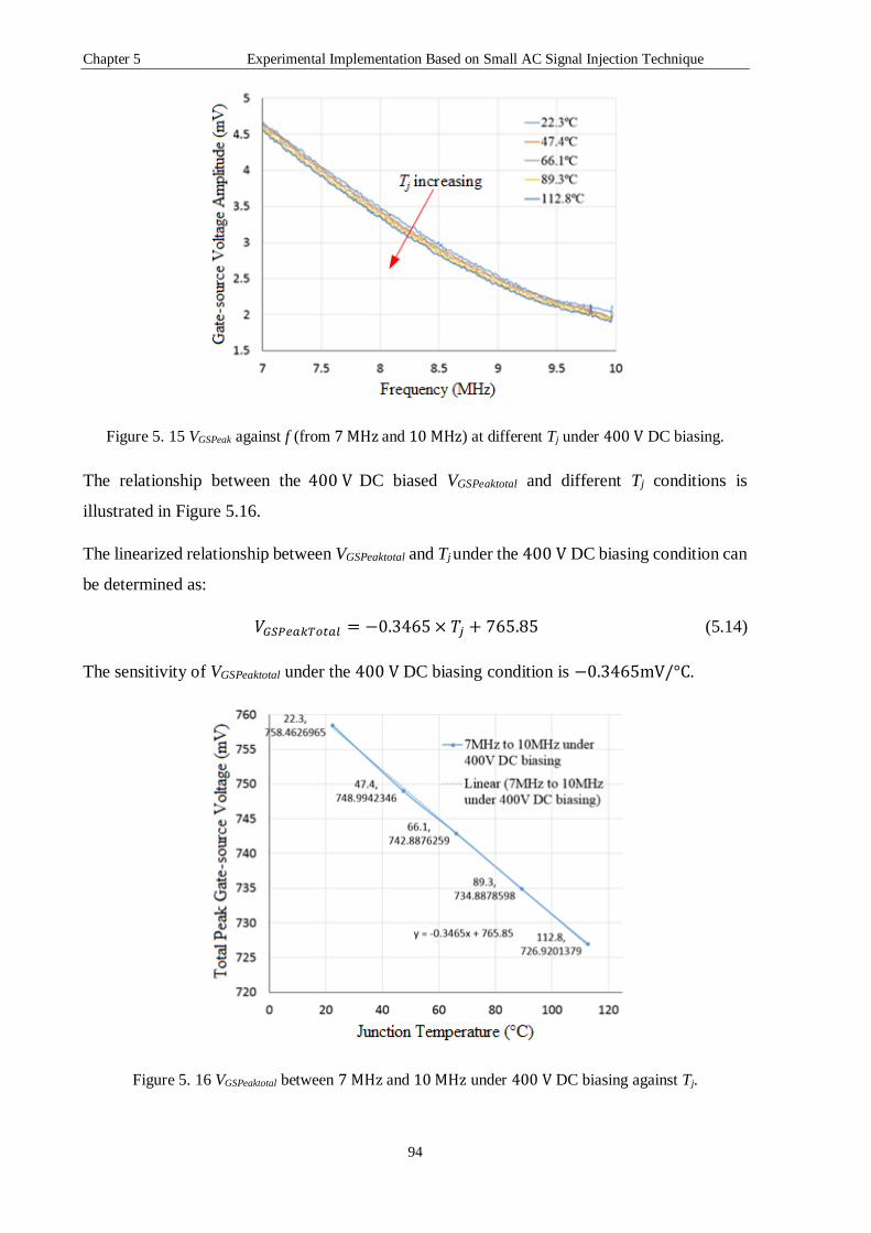
Chapter 5 Experimental Implementation Based on Small AC Signal Injection Technique
94
Figure 5. 15 VGSPeak against f (from 7 MHz and 10 MHz) at different Tj under 400 V DC biasing.
The relationship between the 400 V DC biased VGSPeaktotal and different Tj conditions is
illustrated in Figure 5.16.
The linearized relationship between VGSPeaktotal and Tj under the 400 V DC biasing condition can
be determined as:
𝑉𝐺𝑆𝑃𝑒𝑎𝑘𝑇𝑜𝑡𝑎𝑙 = −0.3465 × 𝑇𝑗 + 765.85 (5.14)
The sensitivity of VGSPeaktotal under the 400 V DC biasing condition is −0.3465mV/°C.
Figure 5. 16 VGSPeaktotal between 7 MHz and 10 MHz under 400 V DC biasing against Tj.

Chapter 5 Experimental Implementation Based on Small AC Signal Injection Technique
95
When a 500 V DC biasing voltage is applied to the drain-source terminal of the SiC MOSFET,
the results for VGSPeak in the frequency range from 7 MHz to 10 MHz are plotted in Figure 5.17.
Figure 5. 17 VGSPeak against f (from 7 MHz to 10 MHz) at different Tj under 500 V DC biasing.
The corresponding values of VGSPeaktotal under the 500 V DC biasing condition are compared
with the changing Tj and plotted in Figure 5.18.
The linearized relationship between VGSPeaktotal and Tj under the 500 V DC biasing condition can
be determined as:
𝑉𝐺𝑆𝑃𝑒𝑎𝑘𝑇𝑜𝑡𝑎𝑙 = −0.3235 × 𝑇𝑗 + 765.62 (5.15)
The sensitivity of VGSPeaktotal under 500 V DC biasing condition is thus−0.3235mV/°C.
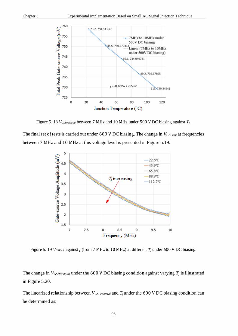
Chapter 5 Experimental Implementation Based on Small AC Signal Injection Technique
96
Figure 5. 18 VGSPeaktotal between 7 MHz and 10 MHz under 500 V DC biasing against Tj.
The final set of tests is carried out under 600 V DC biasing. The change in VGSPeak at frequencies
between 7 MHz and 10 MHz at this voltage level is presented in Figure 5.19.
Figure 5. 19 VGSPeak against f (from 7 MHz to 10 MHz) at different Tj under 600 V DC biasing.
The change in VGSPeaktotal under the 600 V DC biasing condition against varying Tj is illustrated
in Figure 5.20.
The linearized relationship between VGSPeaktotal and Tj under the 600 V DC biasing condition can
be determined as:

Chapter 5 Experimental Implementation Based on Small AC Signal Injection Technique
97
𝑉𝐺𝑆𝑃𝑒𝑎𝑘𝑇𝑜𝑡𝑎𝑙 = −0.32 × 𝑇𝑗 + 766.25 (5.16)
The sensitivity of VGSPeaktotal under the 600 V DC biasing condition is then −0.32mV/°C.
Figure 5. 20 VGSPeaktotal between 7 MHz and 10 MHz under 600 V DC biasing against Tj.
All of the above the DC biasing conditions are compared to investigate the influence of DC
biasing voltage on the estimation of Tj based on the small AC signal injection. As shown in
Figure 5.21, the above 7 different DC biasing conditions are plotted in one chart.

Chapter 5 Experimental Implementation Based on Small AC Signal Injection Technique
98
Figure 5. 21 Comparison of DC biasing conditions for small AC signal injection technique.
As can be seen from Figure 5.21, the trend lines for VGSPeaktotal for different DC biasing
conditions are almost entirely in parallel with each other, which indicates that the slopes of the
trend lines are almost the same. This means that the sensitivity for each DC biasing conditions
are very close to each other. This can be summarized in Table 5.1.
Table 5. 1 Sensitivity of VGSPeaktotal at different DC biasing voltage conditions
DC biasing voltage Sensitivity of VGSPeaktotal
50 V −0.3340 mV/°C
100 V −0.3398 mV/°C
200 V −0.3381 mV/°C
300 V −0.3561 mV/°C
400 V −0.3465 mV/°C
500 V −0.3235 mV/°C
600 V −0.3200 mV/°C
The average sensitivity of the VGSPeaktotal under these seven DC biasing conditions can be
calculated as −0.3369 mV/°C . The highest sensitivity is under 300 V DC biasing, at
−0.3561 mV/°C and the lowest is under the 600 V DC biasing condition at −0.32 mV/°C. The

Chapter 5 Experimental Implementation Based on Small AC Signal Injection Technique
99
difference between the highest and average sensitivity is 0.0192 mV/°C, which is a difference
of about 5.7% . Meanwhile the discrepancy between the lowest sensitivity and average
sensitivity is 0.0169 mV/°C which is a difference of 5%. The sensitivities for the versions DC
biasing conditions remain almost the same within a tolerance range of ±5%.
Another point worth noting is that the absolute VGSPeak at fixed frequency changes due to the
variation in DC biasing voltage. It can be seen from Figure 5.21 that, with increasing DC biasing
voltage, the trend line moves upwards which indicates that at each frequency the VGSPeak value
is higher when the DC biasing voltage is higher. This is due to the fact that the Tj-dependent
Rint is not a lumped resistance but an equivalent resistance of the parasitic capacitance.
b. Biased test under DC biasing voltage with chirp signal injected via gate driver
In the previous section, the small AC chirp signal and the minus DC biasing voltage are both
generated by the function generator. This is a viable solution that can be implemented in a
laboratory environment. However, in order to apply this small signal injection technique in real
applications, the minus bias DC voltage should be provided by a SiC MOSFET gate driver.
Thus, how to superimpose the small signal onto the minus DC bias voltage generated by the
gate driver and then to apply it to the gate terminal of the SiC MOSFET becomes an issue. To
address this issue, a solution utilizing a pulse transformer is proposed, and this is discussed in
detail in the following sections.
In this particular test, a Cree gate driver board for the 2nd generation (C2MTM) SiC MOSFET
(Part number: CRD-001) is utilized to drive the C2M0080120D SiC MOSFET. The basic
schematic of the gate driver is presented in Figure 5.22, and other documents regarding this
gate driver board are presented in Appendix E including specifications and relevant schematics.
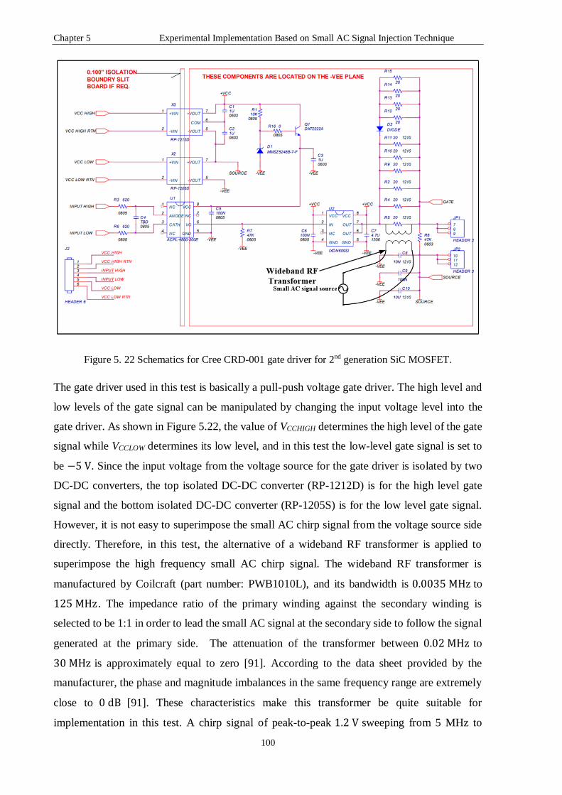
Chapter 5 Experimental Implementation Based on Small AC Signal Injection Technique
100
Figure 5. 22 Schematics for Cree CRD-001 gate driver for 2nd generation SiC MOSFET.
The gate driver used in this test is basically a pull-push voltage gate driver. The high level and
low levels of the gate signal can be manipulated by changing the input voltage level into the
gate driver. As shown in Figure 5.22, the value of VCCHIGH determines the high level of the gate
signal while VCCLOW determines its low level, and in this test the low-level gate signal is set to
be −5 V. Since the input voltage from the voltage source for the gate driver is isolated by two
DC-DC converters, the top isolated DC-DC converter (RP-1212D) is for the high level gate
signal and the bottom isolated DC-DC converter (RP-1205S) is for the low level gate signal.
However, it is not easy to superimpose the small AC chirp signal from the voltage source side
directly. Therefore, in this test, the alternative of a wideband RF transformer is applied to
superimpose the high frequency small AC chirp signal. The wideband RF transformer is
manufactured by Coilcraft (part number: PWB1010L), and its bandwidth is 0.0035 MHz to
125 MHz. The impedance ratio of the primary winding against the secondary winding is
selected to be 1:1 in order to lead the small AC signal at the secondary side to follow the signal
generated at the primary side. The attenuation of the transformer between 0.02 MHz to
30 MHz is approximately equal to zero [91]. According to the data sheet provided by the
manufacturer, the phase and magnitude imbalances in the same frequency range are extremely
close to 0 dB [91]. These characteristics make this transformer be quite suitable for
implementation in this test. A chirp signal of peak-to-peak 1.2 V sweeping from 5 MHz to

Chapter 5 Experimental Implementation Based on Small AC Signal Injection Technique
101
10MHz is injected into the wide-band RF transformer and the input and output signals are
compared and presented in figures illustrated below. In these three figures, the dark-blue curve
is the input signal (channel 1) and the light-blue curve is the output signal (channel 2).
Figure 5. 23 Chirp signal input and output comparison at 5 MHz by using wide-band RF transformer.
It can be seen from Figure 5.23, for the chirp signal at 5 MHz, despite there is a little shift
between the input and output waveforms two waves forms are still almost fully overlapped with
each other. It can be seen that the peak-to-peak value of the input signal is 1.26 V and the output
signal is 1.24 V which means there is a 1.6 % difference which is negligible. In terms of
frequency the input signal is 5.010 MHz and the output signal is 5.038 MHz the difference
between two signals is 0.028 MHz which is also insignificant.
To further exam the capability of the wide-band transformer, waveforms captured by the
oscilloscope around 7.4 MHz and 9.3 MHz are illustrated in Figure 5.24 and 5.25 respectively.
Similar with the results presented in Figure 5.23, the output signal via the wide-band RF
transformer is closely follow the pattern of the input signal.
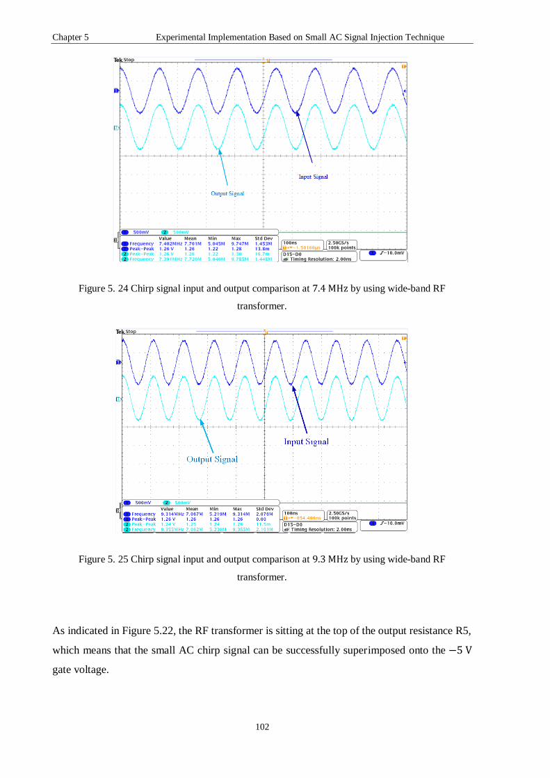
Chapter 5 Experimental Implementation Based on Small AC Signal Injection Technique
102
Figure 5. 24 Chirp signal input and output comparison at 7.4 MHz by using wide-band RF
transformer.
Figure 5. 25 Chirp signal input and output comparison at 9.3 MHz by using wide-band RF
transformer.
As indicated in Figure 5.22, the RF transformer is sitting at the top of the output resistance R5,
which means that the small AC chirp signal can be successfully superimposed onto the −5 V
gate voltage.

Chapter 5 Experimental Implementation Based on Small AC Signal Injection Technique
103
The issue regarding how the gate driver can be used in combination with the small signal
generation device to generate the required chirp signal with minus DC biasing has now been
resolved, and the test can proceed by injecting the small AC chirp signal via the gate driver.
Figure 5.26 shows VGSPeak against frequencies between 7 MHz to 10 MHz under 300 V DC
biasing with an injection signal with a peak-to-peak amplitude of 5 V via the gate driver at
different values of Tj. The reason for using a relatively large value of amplitude of the injection
signal is that it is weakened by the wideband RF transformer which means that the of actual
signal passing into the gate-source terminal of the SiC MOSFET is smaller than the original
signal. This amplitude of the signal is controlled in a suitable range to avoid false triggering.
Figure 5. 26 VGSPeak against f at 300 V DC biasing with injection via gate driver with 5 V peak-to-peak
injection amplitude.
The VGSPeak still shows a negative dependency on Tj, as illustrated in Figure 5.23. The
accumulated VGSPeak is also calculated and plotted in Figure 5.27. As can be seen, the VGSPeaktotal
decrease linearly with t increasing Tj of the DUT.
The relationship between VGSPeaktotal and the corresponding Tj is derived as:
𝑉𝐺𝑆𝑃𝑒𝑎𝑘𝑇𝑜𝑡𝑎𝑙 = −33.44 × 𝑇𝑗 + 30415 (5.16)
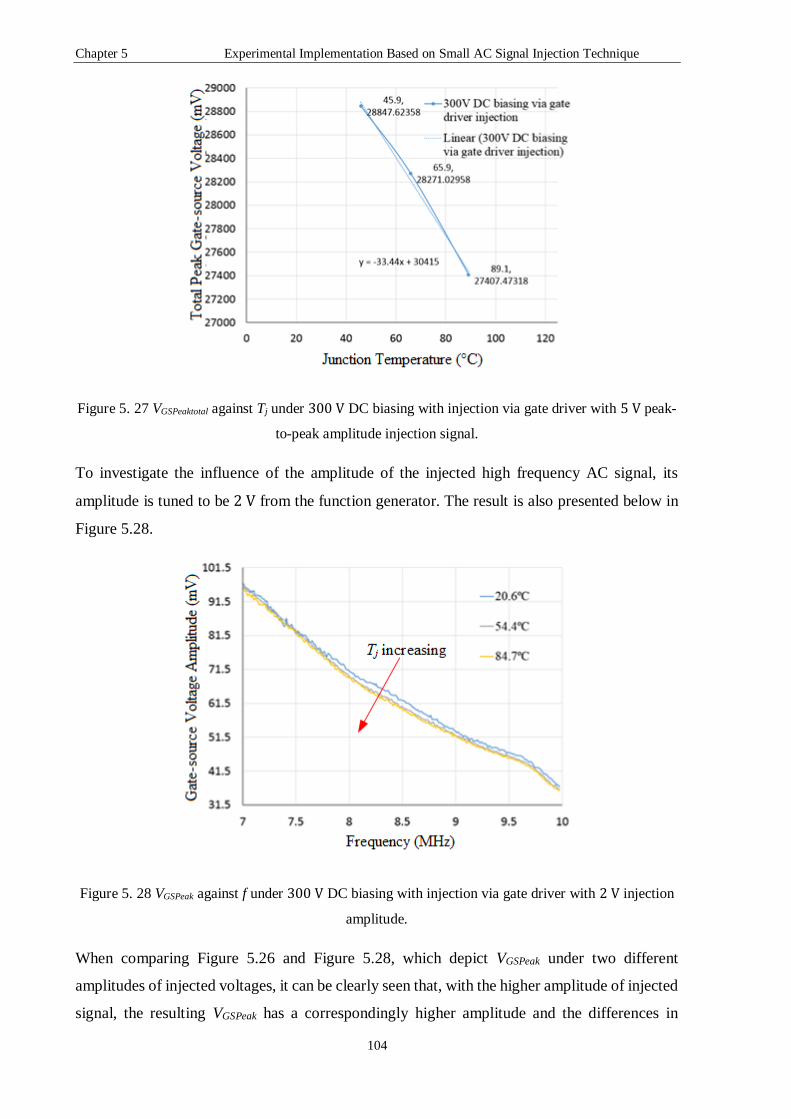
Chapter 5 Experimental Implementation Based on Small AC Signal Injection Technique
104
Figure 5. 27 VGSPeaktotal against Tj under 300 V DC biasing with injection via gate driver with 5 V peak-
to-peak amplitude injection signal.
To investigate the influence of the amplitude of the injected high frequency AC signal, its
amplitude is tuned to be 2 V from the function generator. The result is also presented below in
Figure 5.28.
Figure 5. 28 VGSPeak against f under 300 V DC biasing with injection via gate driver with 2 V injection
amplitude.
When comparing Figure 5.26 and Figure 5.28, which depict VGSPeak under two different
amplitudes of injected voltages, it can be clearly seen that, with the higher amplitude of injected
signal, the resulting VGSPeak has a correspondingly higher amplitude and the differences in

Chapter 5 Experimental Implementation Based on Small AC Signal Injection Technique
105
VGSPeak between two different Tj are also larger. This finally confirms that the sensitivity of the
VGSPeaktotal increases with the higher injected signal amplitude. As represented in Figure 5.29,
VGSPeaktotal is plotted against Tj of the SiC MOSFET and the linearized trend line is also derived
and the relationship between the VGSPeaktotal and Tj can be presented as in equation 5.17:
𝑉𝐺𝑆𝑃𝑒𝑎𝑘𝑇𝑜𝑡𝑎𝑙 = −8.1161 × 𝑇𝑗 + 15849 (5.17)
Figure 5. 29 VGSPeaktotal against Tj under 300 V DC biasing with injection via gate driver with 2 V peak
to peak amplitude injection signal.
The values of sensitivity of VGSPeaktotal against Tj under a 5 V injection signal and 2 V injection
signal is −33.44 mV/°C and −8.1161 mV/ °C respectively. It is obvious that higher amplitude
of injection signal results in a bigger discrepancy in VGSPeaktotal, which means a greater
sensitivity. This phenomenon can be utilized to optimize the sensitivity of the VGSPeaktotal to find
a suitable value that is big enough so as to be easily detected based on state-of-the-art sensor
techniques to generate reasonable sensitivity. Meanwhile the amplitude of the injected signal
should not be so big as exceed the required minus gate voltage in order to avoid the false
triggering of the SiC MOSFET during normal operation.
The boost converter test is carried over based on the Cree/Wolfspeed kit8020-CRD-8FF1217P-
1 evaluation boar[92]. A C2M0080120D SiC MOSFET and a C4D20120D SiC Schottky diode
are used to form a non-synchronous boost DC/DC converter, the schematic is shown in Fig 5.30
that SiC MOSFET is deployed at Q1 position and SiC Schottky diode is located at Q2 position.
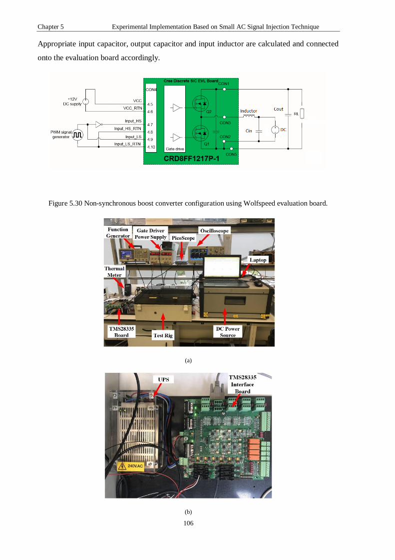
Chapter 5 Experimental Implementation Based on Small AC Signal Injection Technique
106
Appropriate input capacitor, output capacitor and input inductor are calculated and connected
onto the evaluation board accordingly.
Figure 5.30 Non-synchronous boost converter configuration using Wolfspeed evaluation board.
(a)
(b)

Chapter 5 Experimental implementation based on small AC signal injection technique
107
(c)
Figure 5.31 Boost converter test setup: (a) overall test bench; (b) TMS28335 PWM generating board;
(c) test rig inside view.
The overall test bench is presented in Fig 5.31(a). The output of the boost converter is connected
to a viable resistive load. The PWM signal is generated and controlled by using an interface
board developed in Newcastle University with TMS28335 DSP board as shown in Fig 5.31(b).
The output of the interface board is connected to the on-board gate driver of the evaluation
board. Duty cycle can be manipulated via LabView interface in real time depending on the
requirement.
As shown in Fig 5.31(c), the device under test (DUT) is soldered under the evaluation board
and sitting on a voltage-controlled heat-plate, the DUT is isolated from the heat-plate with a
silicon thermal pad. The heat-plate has a resolution of 1°C. The output of the DC/DC converter
is a variable resistive load which has a tuning range between 30ohm and 300ohm.

Chapter 5 Experimental implementation based on small AC signal injection technique
108
Figure 5.32 Measured oscilloscope waveforms of boost converter including output voltage, gate-
source voltage, drain-source voltage and inductor current.
An example of operating voltage and current waveforms under 80% duty cycle operation is
presented in Fig 5.32 Small AC chirp signal sweeping from 5MHz to 10MHz is superimposed
onto the gate signal via a RF transform in parallel with the external gate resistor. As can be seen
from the graph that the boost DC/DC converter is working under CCM mode. The gate-source
voltage is extracted and analysed after the data has been stored in the PC.
The measured temperature is corelated with the die body temperature rise derived by the 3D
thermal model at each temperature steps. The temperature rise value at each temperature are
listed in the table below.
Table 5. 2 Ture junction temperature consider die body temperature rise
Tempeture Step (°C) Die Body Temperature Rise (°C) Measured Tempearture (°C)
25 0.541 33
50 0.547 45
75 0.569 65
100 0.59 82
125 0.65 101
The corelated temperture is calculated by adding the measured temperature with the die body
temprature rise as the true Tj since the thermo coupler is detecting the SiC MOSFET
temperature near the bottom drain pad. There is small fraction of change for each temperature
steps, and by applying the simulated Tj rise induced by the SiC die body would minimise the
error between the true Tj and measured Tj. The corelated Tj and measured off-state gate source
voltage are plotted in the Figure 5.33 illustred as follow.
There is -1.6%, -1.2%, -0.08%, -0.07% and -0.064% temperature difference between the true
Tj and measured Tj at 25°C,50°C,75°C, 100°C and 125°C heat plate temperature conditions
respectively. The estimated ture Tj helps to increase the accuracyof the proposed method.
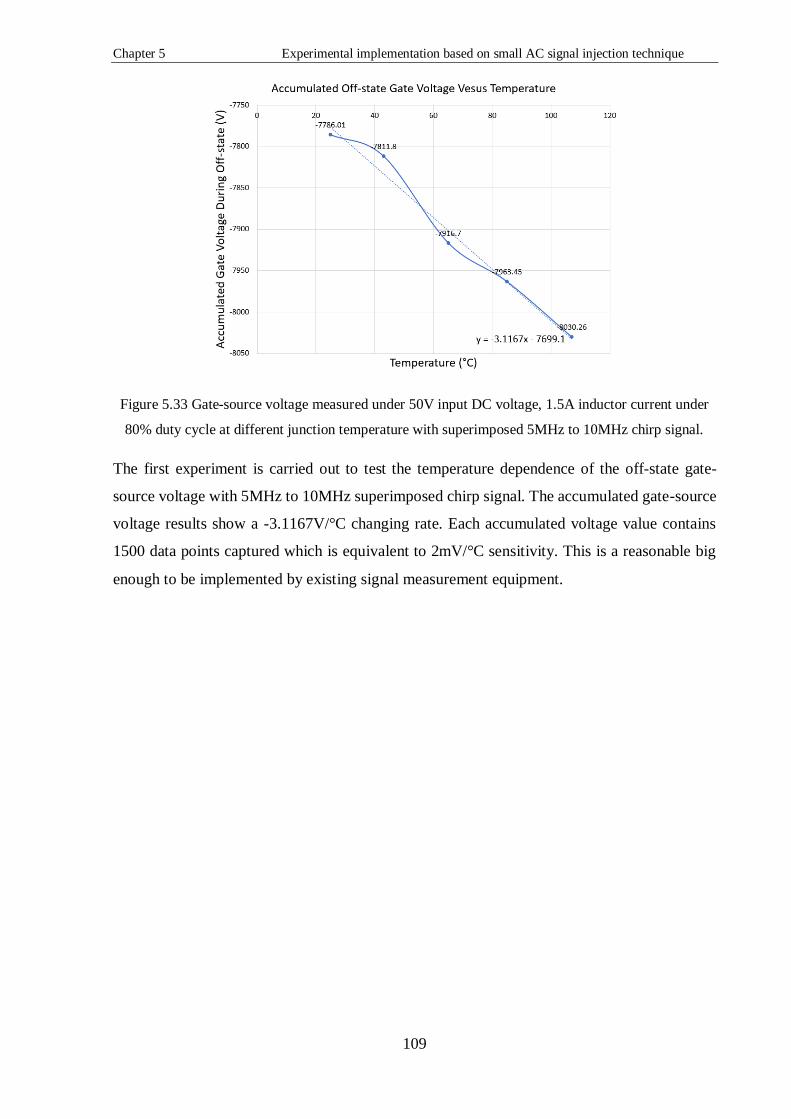
Chapter 5 Experimental implementation based on small AC signal injection technique
109
Figure 5.33 Gate-source voltage measured under 50V input DC voltage, 1.5A inductor current under
80% duty cycle at different junction temperature with superimposed 5MHz to 10MHz chirp signal.
The first experiment is carried out to test the temperature dependence of the off-state gate-
source voltage with 5MHz to 10MHz superimposed chirp signal. The accumulated gate-source
voltage results show a -3.1167V/°C changing rate. Each accumulated voltage value contains
1500 data points captured which is equivalent to 2mV/°C sensitivity. This is a reasonable big
enough to be implemented by existing signal measurement equipment.
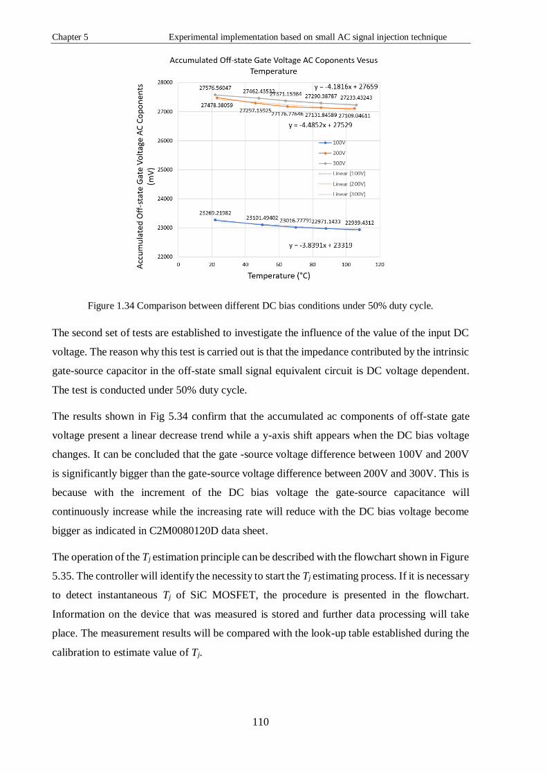
Chapter 5 Experimental implementation based on small AC signal injection technique
110
Figure 1.34 Comparison between different DC bias conditions under 50% duty cycle.
The second set of tests are established to investigate the influence of the value of the input DC
voltage. The reason why this test is carried out is that the impedance contributed by the intrinsic
gate-source capacitor in the off-state small signal equivalent circuit is DC voltage dependent.
The test is conducted under 50% duty cycle.
The results shown in Fig 5.34 confirm that the accumulated ac components of off-state gate
voltage present a linear decrease trend while a y-axis shift appears when the DC bias voltage
changes. It can be concluded that the gate -source voltage difference between 100V and 200V
is significantly bigger than the gate-source voltage difference between 200V and 300V. This is
because with the increment of the DC bias voltage the gate-source capacitance will
continuously increase while the increasing rate will reduce with the DC bias voltage become
bigger as indicated in C2M0080120D data sheet.
The operation of the Tj estimation principle can be described with the flowchart shown in Figure
5.35. The controller will identify the necessity to start the Tj estimating process. If it is necessary
to detect instantaneous Tj of SiC MOSFET, the procedure is presented in the flowchart.
Information on the device that was measured is stored and further data processing will take
place. The measurement results will be compared with the look-up table established during the
calibration to estimate value of Tj.
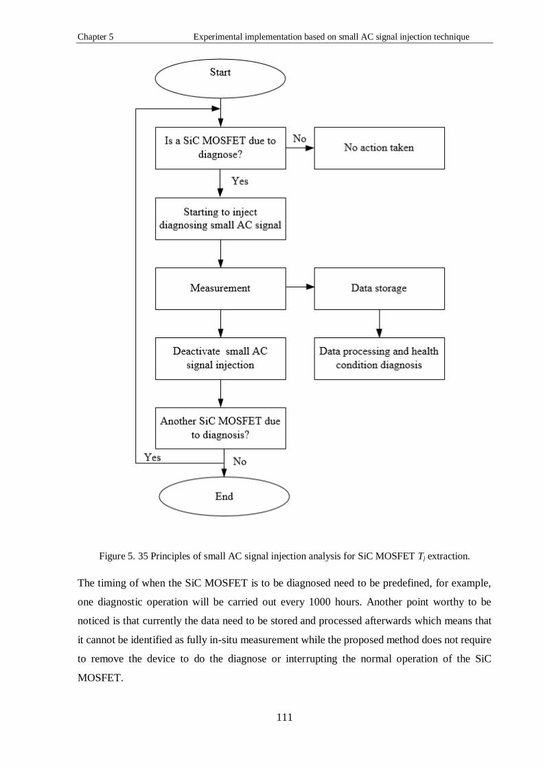
Chapter 5 Experimental implementation based on small AC signal injection technique
111
Figure 5. 35 Principles of small AC signal injection analysis for SiC MOSFET Tj extraction.
The timing of when the SiC MOSFET is to be diagnosed need to be predefined, for example,
one diagnostic operation will be carried out every 1000 hours. Another point worthy to be
noticed is that currently the data need to be stored and processed afterwards which means that
it cannot be identified as fully in-situ measurement while the proposed method does not require
to remove the device to do the diagnose or interrupting the normal operation of the SiC
MOSFET.

Chapter 5 Experimental implementation based on small AC signal injection technique
112
5.2 Conclusion
In this chapter, the experimental set-up utilizing small AC signal injection is presented.
Unbiased, biased experimental tests and finally test based on Cree/Wolfspeed discrete SiC
MOSFET evaluation board are carried out. The values of Tj of the SiC MOSFET can be
extracted by determining the relationship between peak gate-source voltages under small AC
signal injection conditions. The biased DC tests are carried out under two different situations,
where initially the small AC signal is directly injected into the gate terminal of the SiC
MOSFET. For real applications, tests utilizing a gate driver to provide a minus gate voltage in
combination with a superimposed small AC signal are also conducted. The results of both tests
verify the proposed small AC signal injection technique. As presented in the previous section,
the value of Tj of the SiC MOSFET can be derived since VGSPeaktotal is linearly dependent on Tj,
and once data for VGSPeaktotal have been captured at different values of Tj then a look-up table
can be established. Calibration should be performed under different DC biasing conditions and
also based on different injection signal amplitudes in order to match real application conditions.
Finally, the look-up table can be used to determine the value of Tj during the normal operation
of the SiC MOSFET.

Chapter 6 Conclusion and future work
113
Chapter 6 Conclusion and future work
Global warming has been a serious issue for the past several decades. To restrict the
continuously increasing emissions of CO2, many efforts have been made, including the
development of EVs and MEA, to reduce the consumption of fossil fuels. This in turn increases
the need for robust power electronic systems to avoid catastrophic failure.
Si power electronic devices or modules have dominated the power electronic scene and the
physical limitations of Si material have already been reached. In these circumstances, in order
to achieve higher temperature capability, faster switching speed, higher break-down voltage
and lower switching and conduction losses, WBG materials are being developed as potentially
the future of power electronics to replace traditional Si semiconductors. However, the reliability
of WBG semiconductor is still an important issue which needs to be addressed. In this thesis, a
SiC discrete MOSFET is used as the device that being studied.
Traditional Tj estimation methods are reviewed including direct temperature measurement
methods, indirect temperature measurement methods and thermal model-based methods. Each
type is presented in detail and its advantages and disadvantages are also listed. Among those
methods, the TSEP-based indirect temperature measurement method is preferred because there
is no requirement to modify the power device or module, it is non-intrusive, and with a proper
set-up it will not interfere with the normal operation of the power electronic system. So state-
of-art TSEPs are analysed in detail and the results show that these methods are not entirely
suitable for SiC discrete MOSFET, due to the unique physical behaviour of SiC material.
Thus, in this thesis a new method based on small AC signal analysis is proposed to extract the
Tj of the SiC discrete MOSFET. The proposed method is non-intrusive and will not interfere
with the normal operation of the MOSFET. A high frequency, small amplitude AC chirp signal
is superimposed onto the negative biasing gate voltage by using a high frequency pulse
transformer during the off state of the SiC discrete MOSFET. The frequency response of the
gate-source voltage is extracted and analysed to find the change in internal gate resistance (Rint)
induced by the variation in Tj. By establishing a look-up table of the relationship between Rint
and Tj, it is possible to estimate the value of Tj of the SiC discrete MOSFET online.
To achieve the proposed method, an equivalent small AC signal circuit is established and the
values for all individual parasitic components are calculated. The equivalent circuit model is
simulated in LTspice and an experimental test is achieved by using an impedance analyser. The

Chapter 6 Conclusion and future work
114
results of both simulations and experiments are compared and prove that the model is precise
enough for use. After the validation of the model, further simulations and experimental tests
are carried out under unbiased and biased conditions. The results are in good agreement with
the simulation results.
In this work, the experiments are only performed on a single SiC discrete MOSFET in a simple
DC bias topology and in a boost converter topology. Thus, more research should be conducted
in the future and should mainly focus on the following aspects.
In the test, due to the large amount data collected from the experiment, it is hard to process the
data immediately. The data must be stored and processed afterwards, which means that values
of instantons Tj cannot be derived instantaneously. Further efforts should be made to establish
improvements in signal processing to calculate the value of Tj simultaneously with the data
acquisition.
The proposed technique might not be applicable to other SiC devices like SiC IGBT, since the
physical topology of SiC MOSFET and SiC IGBT are not completely the same, so the
relationship between the Tj and measured gate-source voltage under superimposed small AC
signal would be different. Thus, if there is need to apply this method to SiC IGBT, delicated
calibration should be carried out to examine the feasibility.
Although the proposed technique is designed to detect the value of Tj for SiC discrete
MOSFETs, it should be able to be applied to SiC MOSFET modules as well. Simulation work
has been carried out to examine proposed method. The implementation of this method would
be more complex since small AC signal injection need to be established for each MOSFET in
the power module via their gate driver respectively. In addition, the parallel structures of SiC
MOSFET modules may lead to challenges if the superimposed signal enters the impedance loop
of other chips in parallel, making it difficult to extract the Tj of the targeted chip accurately.
Similar to the above issue, if the values of parasitic components in the topology are of similar
magnitudes as the parasitic components in the gate-source loop of the SiC MOSFET, the
injected signal might pick up the change in the parasitic components of the topology due to
degradation. This will result in inaccurate Tj estimation, and for this reason further research
should be conducted to decouple the effects of the parasitic components of the topology from
the parasitic components of the SiC MOSFET.

Appendix A
115
Appendix A: State-of-art of TSEPs
A.1 Introduction
The main difficulty in accomplishing temperature measurement is to extract the relevant
thermal information while devices are in operation. Gel in the module and the packaging of
devices do not allow direct measurement methods like the use of an infrared camera or
embedded thermal sensors. TSEPs are seen as an alternative as they measure voltages and
currents at the terminals of the device. Changes in voltage and current can be translated into
temperature by knowing the relationship between the physical properties and their temperature
dependencies. TSEPs are widely used to extract the thermal information from chips [4]. In the
following sections, state-of-art TSEPs are described and summarized.
A.2 Steady-state TSEPs
TESPs can be categorized as steady-state TSEPs and dynamic TSEPs. Steady-state TSEPs refer
to the fact that parameters are extracted during either the on-state or the off-state of the power
device, and dynamic TSEPs are captured during the switching transient periods of the power
device [93]. In the next section, the steady-state TSEPs which have been proposed by
researchers in the past several decades are presented.
a. Saturation current (Isat)
The first steady-state TESP presented here is the saturation current (Isat) which can be defined
as the collector current [94, 95] when:
𝑉𝐶𝐸𝑠𝑎𝑡 = 𝑉𝐺𝐸 − 𝑉𝑇𝐻 (A1)
and Isat can be expressed as in equation A2:
𝐼𝑠𝑎𝑡 = ((1 + 𝛽𝑃𝑁𝑃)𝑢𝑛𝑠(𝑇𝑐ℎ0)𝐶𝑂𝑋𝑍𝑐
2𝐿𝑐× (𝑉𝐺𝐸 − 𝑉𝑇𝐻(𝑇𝑐ℎ0))2 (A2)
where Isat is the saturation current, βPNP is the current gain of the bipolar transistor in the IGBT
(for MOSFETs: βPNP =0), µns is the surface mobility of electrons in the channel, Cox is the oxide
capacitance, ZC is the channel width, LC is the channel length, VCEsat is the collector-emitter
saturation voltage, VGE is the gate-emitter voltage and VTH is the threshold voltage. The
relationship between the Isat and the Tj has been presented for different VGE and VCE conditions
as shown in Figure A1 [96].

Appendix A
116
Figure A 1 Isat value as a function of Tj at different voltage conditions [96].
It can be seen from Figure A1 that, with the increment of Tj, Isat increases accordingly. Beside
this, the collector-emitter voltage VCE and the gate-emitter voltage VGE influence Isat too, as
shown in the figure. Isat increases slightly only when VCE doubles (10 V to 20 V), which
indicates that VGE is the dominant parameter that affects Isat at fixed Tj. Another aspect worth
noting is that the sensitivity of Isat against Tj become bigger with higher VGE.
b. Collector leakage current (Ileak)
Another current type of TSEP is the collector leakage current (Ileak). Ileak is defined as the passing
collector current when gate-emitter is shorted and rated voltage is applied to collector-emitter
[97]. Ileak can be represented as shown in equation A3:
𝐼𝑙𝑒𝑎𝑘 = 𝑞𝐴𝑛𝑖
2
𝑁𝑜√
𝐷𝑛
𝜏𝑛+
𝑞𝐴𝑛𝑖𝑥𝑑
𝜏𝑛 (A3)
where A is the junction area, ni is the intrinsic carrier doping concentration, τn is the lifetime of
the space charge region, Dn is the diffusion coefficient of an electron and lastly xd is the diffuse
length at high temperature. Some practical results have been published [97] as illustrated in
Figure A2 where a 1200 V, 50 A IGBT was used.

Appendix A
117
Figure A 2 Comparison of collector leakage current under different VCE [97].
As shown in Figure A2, at low Tj (roughly below 150 ˚C) there is only a small change in Ileak.
When Tj goes beyond 150 ˚C a significant increment of Ileak is observed.
c. On-state voltage drop (VCE(on))
VCE(on) is a measures of the voltage drop between the collector-emitter terminals during the
IGBT’s on-state. A defined measurement current (Im) is flowing through the collector-emitter.
The voltage builds up due to inner resistance and intrinsic voltage across the built-in PN
junction [97]. The equation relating VCE(on) to Im is approximated as [97]:
𝑉𝐶𝐸(𝑜𝑛) = 𝑉𝐶𝐸0 + ∆𝑉𝐶𝐸0(𝑇𝑗 − 𝑇𝑗0) + 𝐼𝑚[𝑟0 + ∆𝑟0(𝑇𝑗 − 𝑇𝑗0)] − 𝛼𝑔𝑒 ∙ ∆𝑉𝐺𝐸 (A4)
where VCE(on), Tj, Im and VGE represent the on-state voltage drop, junction temperature,
measurement current and gate-emitter voltage respectively, VCE0 and r0 are the on-state voltage
drop and ohmic resistance at the reference junction temperature Tj0, ΔVCE0 and Δr0 are the
temperature coefficients for VCE0 and r0 correspondingly, and ΔVge is gate-emitter voltage
difference. From equation A4, VCE(on) can be described as a function of Tj, Im and Vge. If it is
possible to keep Im and Vge constant, then the above equation can be simplified and VCE(on) is
only influenced by Tj, as shown in equation A5:
𝑉𝐶𝐸(𝑜𝑛) = 𝑉𝐶𝐸0′ + ∆𝑉𝐶𝐸0(𝑇𝑗 − 𝑇𝑗0) (A5)
Where 𝑉𝐶𝐸0′ is the on-state voltage drop at the reference Tj, Im and Vge.
In this way, Tj can be effectively estimated by obtaining the value of VCE(on).
As shown in Figure A3, five different Im current values are injected into the collector-emitter
and the corresponding VCE(on) is plotted [93].

Appendix A
118
Figure A 3 VCE(on) of an IGBT as a function of Tj for different Im [93].
It is clear from Figure A3 that, with increasing Tj, VCE(on) changes linearly.
A.3 Dynamic TSEPs
Dynamic TSEPs are captured during the switching transient period of power electronics devices
[98].
a. Transconductance (gm)
Transconductance (gm) is the gain of the transistor and refers to the magnitude of output current
(collector current IC) obtained for a given input voltage (gate voltage VGE) [99]. It can be
expressed as in equation A6:
𝑔𝑚 =𝑑𝐼𝐶
𝑑𝑡⁄
𝑑𝑉𝐺𝐸𝑑𝑡⁄
=1
1−𝛽𝑝𝑛𝑝(𝑇)[𝜇(𝑇)𝐶𝑂𝑋 ×
𝑊
𝐿(𝑉𝐺𝐸 − 𝑉𝑡ℎ𝑟𝑒𝑠ℎ𝑜𝑙𝑑(𝑇))] (A6)
Where βpnp(T) is the current gain of the p-n-p transistor structure within an IGBT, which is
temperature-dependent, μ(T) is the electron channel mobility (in centimetres squared per volt
per second (cm2/V · s)) and the dependence on temperature is presented in equation A7:
𝜇(𝑇) = 1350 × (𝑇300⁄ ) − 2.42 (𝑤ℎ𝑒𝑛 𝑇 ≥ 200𝐾) (A7)
COX is the oxide capacitance (in Farads per centimetre square (F/cm2)), and W and L are the
channel width and length respectively (in centimetre (cm)).

Appendix A
119
Figure A 4 Transconductance of a 3 kV 1200 A IGBT Module [100].
In Figure A4, it can be observed that, for a gate voltage below 7.8 V, transconductance increases
with temperature, whereas for higher VGE values, gm decreases with temperature and exhibits
larger signal dynamics, especially in the highest VGE range.
b. Threshold voltage (VTH)
VTH is the gate voltage at the instance when the IGBT turns on and collector current (IC) begins
to flow [99]. VTH can be described as in equation A8 below:
𝑉𝑡ℎ = 𝑉𝐹𝐵 + 2∅𝐹𝐵 +𝑄𝐵𝑚𝑎𝑥
𝐶𝑂𝑋= 𝑉𝐹𝐵 + 2∅𝐹𝐵 +
√2 0 𝑠𝑞𝑁𝐴𝑚𝑎𝑥(2∅𝐹𝐵)
𝐶𝑂𝑋 (A8)
where VFB is the flat-band voltage, 2ΦFB is surface potential, NAmax is surface concentration,
amd Cox is gate oxide capacitance [101]. In the above equation, ΦFB is the most temperature-
dependent parameter and is given by:
∅𝐹𝐵 =𝑘𝑇
𝑞ln
𝑁𝐴𝑚𝑎𝑥
𝑛𝑖 (A9)
Where T is the channel or junction temperature.

Appendix A
120
Figure A 5 Turn-on transient behaviour of VGE at different Tj [102]
In Figure A5, it can be clearly seen that, during the turn-on process of an IGBT, the instance
where IC begins to flow is delayed with increasing Tj, and the point where IC starts to be bigger
than 0 A shifts towards the right on the graph. The corresponding VGE can be detected and
plotted to find VTH accordingly.
Figure A 6 Change in IGBT VTH with increasing Tj [100].
It is shown in Figure A6 that, for the IGBT used in the test, VTH decrease homogeneously with
the increment of Tj. For the case in Figure A7, VTH was extracted under various IC and VCE
conditions as illustrated. Overall, the VTH value declines along with the rise in Tj. For higher
values of IC, VTH is slightly higher but for different VCE levels there is merely a change in VTH at
fixed Tj.

Appendix A
121
Figure A 7 VTH as a function of Tj for different IC and VCE value [98]
c. Gate voltage miller plateau width during turn-off
The Miller plateau exists due to the effective capacitance between the gate and collector in the
case of the IGBT (CGC), and for a MOSFET it is the capacitance between the gate and drain
(CGD). The time duration of the Miller plateau (tMiller) can be expressed as in equation A10:
𝑡𝑀𝑖𝑙𝑙𝑒𝑟 =𝑅𝐺∙𝐶𝐺𝐶∙(𝑉𝑑𝑐−𝑉𝑜𝑛)
(𝐼𝐿
𝑔𝑚+𝑉𝑡ℎ)
(A10)
where tMiller is the duration of the Miller plateau, RG is the total gate resistance which is
composed of internal and external resistance, CGC is the gate-collector capacitance (Miller
capacitance), Vdc is the DC-link voltage, Von is the on-state voltage, IL is the load current, gm is
the transconductance, and VTH is the threshold voltage. From the equation above, it can be seen
that tMiller is proportional to CGC. The effect of variation in Tj upon Von can be neglected because
the change of Von is much smaller in comparison with VDC. RG is also Tj-dependent and increases
with Tj due to the decline in electron mobility, which in turn increases the internal gate
resistance. Those effects together result in the fact that tMiller increases with rising Tj.
A typical VGE waveform found [103] during the IGBT turn-off is plotted as shown in Figure
A8. As illustrated in Figure A8, it can be observed that, for a fixed 25˚C Tj step increase, the
end points of the Miller plateau are shifted to the right-hand side while the starting points of the
plateau almost remain the same, which indicates that the time period becomes bigger with the
rise in Tj.

Appendix A
122
Figure A 8 VGE waveforms at different temperatures for an IGBT measured at a 600 V, 100 A
switching condition [103].
The value of tMiller at various Tj levels [103], are also plotted as shown in Figure A9, which
indicates that tMiller increase linearly with rising Tj.
Figure A 9 Time difference between the first falling edge and second falling edge of the Vge waveform
at the 600 V, 100 A switching condition [103].
d. Turn-on delay time (td(on))
The td(on) can be defined as the specific period between the triggering instance of the gate driver
or the instance when VGE reaches a certain level, for example 10% of its final value, and the
instance when IC has reached a given level such as 10% of its final value when the device is
fully on [104]. Mathematically, td(on) can be presented as shown in equation A11:

Appendix A
123
𝑡𝑑(𝑜𝑛) = 𝑅𝐺(𝐶𝐺𝐸 + 𝐶𝐺𝐶) ln(1
1−𝑉𝑇𝐻𝑉𝐺𝐸
) (A11)
where RG is the gate resistance, CGE and CGC are parasitic capacitances and VTH is the threshold
voltage.
As illustrated in Figure A10, the dashed lines indicate the duration of td(on).
Figure A 10 Typical turn-on process of IGBT [67].
Test results [102] show the influence of the load current and applied DC voltage on td(on) while
Tj is changing.
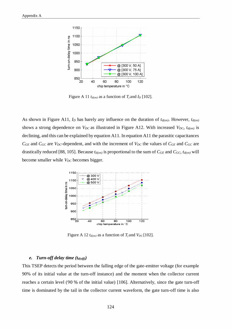
Appendix A
124
Figure A 11 td(on) as a function of Tj and ID [102].
As shown in Figure A11, ID has barely any influence on the duration of td(on). However, td(on)
shows a strong dependence on VDC as illustrated in Figure A12. With increased VDC, td(on) is
declining, and this can be explained by equation A11. In equation A11 the parasitic capacitances
CGE and CGC are VDC-dependent, and with the increment of VDC the values of CGE and CGC are
drastically reduced [88, 105]. Because td(on) is proportional to the sum of CGE and CGC, td(on) will
become smaller while VDC becomes bigger.
Figure A 12 td(on) as a function of Tj and VDC [102].
e. Turn-off delay time (td(off))
This TSEP detects the period between the falling edge of the gate-emitter voltage (for example
90% of its initial value at the turn-off instance) and the moment when the collector current
reaches a certain level (90 % of the initial value) [106]. Alternatively, since the gate turn-off
time is dominated by the tail in the collector current waveform, the gate turn-off time is also

Appendix A
125
defined as the time taken for the anode current to decay to 90 % of its original value after the
termination of the gate pulse, as illustrated below in Figure A13 [100].
Figure A 13 Typical turn-off process of IGBT [67].
Previous results [67] presenting variations of td(off) with Tj and IL and results presenting
variations of td(off) with Tj and VDC are illustrated in Figures A14 and A15, respectively.
It can be seen from Figure A14 that, for fixed IL and VDC test conditions, td(off) is proportional to
Tj, as shown. However, td(off) is not only dependent on Tj but is also related to the load current
as well, as the fixed Tj, td(off) drops when IL increases. In Figure A15, the results shown prove
that, for fixed IL, td(off) will increase with VDC.

Appendix A
126
Figure A 14 Variation in td(off) with Tj and IL: (a)VDC=1400 V and (b) VDC=1600 V [67].
Figure A 15 Variation of td(off) with Tj and VDC: (a)IL=1000 A and (b) IL=1200 A [67].
f. dVCE/dt slope during turn-off
The changing rate of VCE during the turn-off state has also been proposed as a dynamic TSEP
[107]. The dVCE/dt slope can be expressed as in equation A12:
𝑑𝑉𝐶𝐸
𝑑𝑡=
1
𝜏𝐺(
𝑉𝐺𝐸(𝑂𝑁)−𝑉𝐺𝐺(𝑂𝐹𝐹)
1+(𝐶𝑂 𝑔𝑚𝜏𝐺⁄ )) (A12)
Where τG is the time constant equal to RG.CGC, VGG(OFF) is gate drive voltage during turn-off
state, VGE(ON) is the gate-emitter voltage at the instant of Miller plateau during turn-off, CO is
the charge extraction capacitance.

Appendix A
127
In Figure A16, the relationship between dVCE/dt and Tj at two different VDC conditions is
illustrated [107]. It can be seen from both graphs that, at fixed VDC, dVCE/dt shows a negative
co-efficient against Tj.
Figure A 16 Measured dVCE/dt values and linear fitted curves against Tj for varying IL at: (a) VDC of
160 V; (b) VDC of 300 V [108].
g. dIC/dt slope during turn-on
As shown in Figure A5 and described in the previous section, at fixed VCE the instantaneous
change in IC is proportional to the instantaneous change of VGE, and the proportionality factor
is represented as gm as shown in equation A13:
𝑑𝐼𝐶
𝑑𝑉𝐺𝐸=
𝑑𝐼𝐶
𝑑𝑡×
𝑑𝑡
𝑑𝑉𝐺𝐸= 𝑔𝑚 (A13)
Substituting equation A6 in equation A13, dIC/dt can be obtained as:
𝑑𝐼𝐶
𝑑𝑡=
𝑑𝑉𝐺𝐸
𝑑𝑡×
1
1−𝛽𝑝𝑛𝑝(𝑇)[𝜇(𝑇)𝐶𝑂𝑋 ×
𝑊
𝐿(𝑉𝐺𝐸 − 𝑉𝑡ℎ𝑟𝑒𝑠ℎ𝑜𝑙𝑑(𝑇))] (A14)
where βPNP is the gain in the inherent bipolar transistor, μ is the mobility, and W/L is the ratio
between the width and the length of the MOS channel [106].
A graph presenting the relationship between dIC/dt and Tj at two different VGE conditions from
a previous study is illustrated [109] in Figure A17. The unique performance of dIC/dt is that, at
lower VGE (10 V) it is positively proportion to Tj but at higher VGE (14.2 V) it here is negatively
proportion to Tj.

Appendix A
128
Figure A 17 The Measured dIC/dt at two different gate voltages [109].
h. Collector current tail (Itail) during turn-off
Itail is generally defined as that part of IC waveform where IC continues to flow after an initially
abrupt fall. As shown in Figure A18, Itail starts when the rate of change of the collector current
is distinctly reduced. Itail appears due to the recombination of minority carriers in the IGBT
[110] Depending on the technology of the IGBT, the magnitude and duration of Itail can have a
strong dependence on temperature [111].
Figure A 18 Turn-off waveform of a commercial IGBT at 150 ˚C, rated current (IRG7IC23FD) [110].

Appendix A
129
Figure A19 illustrates Itail behaviour during the IGBT turn-off period under different Tj. It can
be observed from the graph that rate of change of Itail becomes smaller, which means that it
takes more time for the Itail to drop to a certain current level at higher Tj.
Figure A 19 Behavior of Itail at different Tj [101].
A.4 Other TSEPs
Other than the steady-state and dynamic TSEPs, there are TSEPs that fall in between these two
categories. In this section, three of those kinds of TSEP are briefly introduced.
a. Power loss dissipation (Pdlss)
Pdlss is the total loss, which takes into account both switching losses and conduction losses. The
relationship between Pdlss and Tj can be described as shown in equation A15:
𝑇𝑗 = 𝑇𝐶 + 𝑃𝑑𝑙𝑠𝑠 ∙ 𝑍𝑡ℎ(𝐽𝐶) (A15)
where TC and Tj are the case and junction temperatures respectively and Zth(JC) is the equivalent
thermal impedance between the junction and the case of the IGBT [112].
TC is acquired by applying a thermal sensor at the bottom surface of the base-plate under the
IGBT chip to improve the accuracy of Tj estimation [112].
One study [102], Pdlss was measured only at turn-on transients under different Tj conditions and
the results are presented in Figure A20. It can be seen that, with the increase in Tj, Pdlss becomes
bigger.

Appendix A
130
Figure A 20 Energy dissipation at turning-on as a function of Tj [106].
b. Internal gate resistance (Rint)
Rint is not identical in its properties to the external gate resistance due to the fact that Rint is
generally considered to be a distributed parameter rather than a lumped resistance, and it is the
result of a combination of individual cells in the die substrate [50]. Rint is a function of mobility
and is proportional to 1/μ, where μ is the channel mobility [106]. Since μ decreases with rising
Tj, resistance increases. Hence internal resistance can be used as a TSEP.
c. Breakdown voltage (Vb)
The occurrence of a temperature dependent avalanche breakdown has been confirmed [9] when
an increasing blocking voltage capability was found with increasing Tj. Vb is given by equation
A16:
𝑉𝑏 = 𝑉𝑎(1 − 𝛼)1/𝑛 (A16)
Where Va is the avalanche breakdown voltage, α is the base transport factor and n is a constant.
α can be expressed as:
𝛼 =1
cosh (𝑊/√𝐷𝑝𝜏𝑝) (A17)
Where W is the un-depleted base width and Dp and τp are the hole diffusion coefficient and
carrier lifetime respectively. For an abrupt junction, the avalanche breakdown voltage Va can
be approximated to:
𝑉𝑎 = 5.34 × 10¹³ × (𝑇𝑗
300)0.35 × 𝑁𝑏
−0.75 (A18)

Appendix A
131
It can be seen from equation A18 that Va is a function of Tj and base-doping concentration (Nb).
If equations A17 and A18 are substituted into equation 16, it can be shown that Vb is Tj-
dependent.
A IGBT with a rated voltage of 600 V has been tested [111] to investigate the relationship
between the value of the avalanche breakdown and Tj. The values of avalanche breakdown
voltage at different values of Tj are listed in Table A1.
Table A 1 Avalanche breakdown voltage under different Tj conditions [111]
Tj (˚C) 25 75 125 150
Vb (V) 805 840 875 890
From the test result in Table A1, the value of the avalanche breakdown voltage of the tested
IGBT increases with temperature and shows a sensitivity of 0.7 V/°C.
A.1 Conclusion
Tj has a big impact on both the efficiency and reliability of a power module, and consequently
knowledge of chip temperature is of paramount importance. In this section, state-of-the-art
TSEPs are presented. TSEPs allow the indirect measurement of Tj non-intrusively and can
therefore be applied in-situ. There are a large number of TSEPs, but no simple and generalized
solution exists today for online junction temperature measurements. Dynamic TSEPs tend to
suffer from EMI problems, and steady-state TSEPs require expensive sensors. It is therefore
necessary to direct research efforts in this domain in order to continue the progression of
condition monitoring and the temperature-based control of power converters.

Appendix B
132
Appendix B: State-of-art Gate Driver Topologies
B.1 Comparison of Si and SiC MOSFET gate drivers
In this appendix, three basic gate driver structures are introduced and then the gate driver for Si
and SiC MOSFET devices are compared and discussed.
Gate drivers can be divided into three basic types: voltage source-based, current source-based
and resonant-based [113]. Voltage source-based gate drivers include the push-pull output and
bootstrap capacitor as well as other types of drivers and this type of gate driver can tune its
output voltage [114]. The current source-based gate drivers include the current mirror-based
and inductor-based current source gate drivers and this type can manipulate the output current
[114]. The operation of both voltage source-based and current source based gate drivers are
explain in detail in the following sections.
a. Push-pull voltage source gate driver
One of the advantages of the push-pull gate driver is that controlling the turn-on or turn-off
states is a relatively simple process and fast hard switching can be achieved [115]. In the case
of the SiC MOSFET, in order to fully turn on the device, the gate source voltage VGS is usually
set to be +20 V, and to properly turn off the device −2 to −10 V is required [21]. To form a
push-pull voltage gate driver, one N-type MOSFET is employed to pull-up the voltage during
the turn-on process and one P-type MOSFET is implemented to pull-down the voltage at turn-
off. Figure B1 shows a dynamic equivalent circuit for a push-pull gate driver. The equivalent
circuit includes a logic buffer in the input stage to limit the input PWM signal current rating, a
push-pull output stage, and loop parasitic Rg1, Rg2, Lg1, Lg2 as well as gate driver resistance are
presented.
Figure B 1 Push-pull voltage source gate driver.

Appendix B
133
During the turn-on transient, as shown in Figure B2, the MOSFET M1 in the logic buffer is
turned on when the external turn-on signal is trigged. Once the M1 is fully turned on, the gate
driver pull-up switch M3 consequently turns on, and as a result the SiC MOSFET gate terminal
is then connected to the +20 V and the gate is charged by the current IGON that passes through
R1. During the turn-off transient, as illustrated in Figure B3, the M4 is turned on after the M2 in
the logic buffer is turned on when the external turn-off signal is activated, and the gate is then
connected to −5 V and the gate discharges with a turn-off current IGOFF.
Figure B 2 Push-pull gate driver turn-on transient.
Figure B 3 Push-pull gate driver turn-off transient
b. Current mirror based current gated driver
WBG semiconductors have a smaller gate charge in comparison with traditional Si devices, and
so a large drain current overshoot is induced due to the ultra-fast turn-on transient [116, 117].
This fast turn-off transient would cause a sizeable VDS overshoot if the parasitic parameters
were not carefully handled [118, 119]. The device’s degradation might be accelerated due to
the aforementioned overshoots and extra switching losses would potentially be produced as

Appendix B
134
well. A current mirror based current source gate driver is able to control the output current and
achieve better switching behaviour. As shown in Figure B4, a current mirror set-up formed by
multiple P-type bipolar junction transistors (BJTs) is applied to the current-source gate driver.
In this configuration, the current mirror BJTs (B1 and B2), the current mirror activating
MOSFET M1, the pull-down MOSFET M2, gate driver resistance and the parasitic of the circuit
layout are depicted. By changing the values of reference resistance Rref, the gate driver output
current mirror can be tuned in a controlled manner. The current mirror is turned on by switch
M1 and then +20 V is connected to the SiC MOSFET gate terminal, as shown in Figure B5. To
turn off the SiC MOSFET, the M2 is turned on and the SiC MOSFET will then be connected to
−5 V, as illustrated in Figure B6.
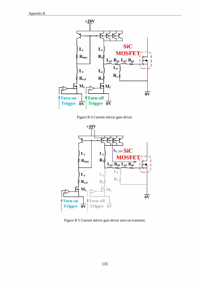
Appendix B
135
Figure B 4 Current mirror gate driver.
Figure B 5 Current mirror gate driver turn-on transient.

Appendix B
136
Figure B 6 Current mirror gate driver turn-off transient.
c. Current source gate driver with a regulated inductor stage
A current source gate driver implemented with an inductor has been proposed [113], and its
topology is presented in Figure B7. An H-bridge configuration is formed by four switches (M1,
M2, M3 and M4) and their antiparallel diodes (D1, D2, D3 and D4) and the load is an air-core
inductor acting as the load of the H-bridge set-up. In this configuration, the SiC MOSFET can
be turned on or off with a non-zero pre-charged current by deliberately controlling these four
switches. The excess energy would be saved in the inductor during the turn-on and turn-off of
the SiC MOSFET and this would then be returned to the 20 V power supply.

Appendix B
137
Figure B 7 Inductor-based current source gate driver.
The turn-on and turn-off processes are explained below in detail.
The turn-on process can be divided into 4 steps:
Step 1: Prior to the charging of the SiC MOSFET gate, switches M2 and M3 are turned on so as
to charge Lair so as to establish the current potential as shown in Figure B8.
Figure B 8 Inductor-based gate driver turn-on transient: step 1.

Appendix B
138
Step 2: As illustrated in Figure B9, the level of current established in Lair can be accurately controlled
by manipulating the switching-off of M3. M3 is turned off while Lair is charged to the desired current
level. The current is then injected into the gate terminal of the SiC MOSFET from the inductor.
Figure B 9 Inductor-based gate driver turn-on transient: step 2.
Step 3: The remaining energy stored in inductor Lair is subsequently sent back to the +20V
voltage supply via the anti-parallel diodes D4 and D1 when the gate voltage VGS reaches +20V.
During this process, M1 is switched on following the gate signal and the current that fed back
to the power supply is able to pass through the anti-parallel diode D4 and switch M1, as shown
in Figure B10.
Figure B 10 Inductor-based gate driver turn-on transient: step 3.

Appendix B
139
Step 4: During the on-state of the SiC MOSFET, switch M1 is also fully turned on in order to
ensure that the gate terminal of the SiC MOSFET is always connected to the +20 V supply, as
indicated in Figure B11.
Figure B 11 Inductor-based gate driver turn-on transient: step 4.
The control strategy for switches M1, M2, M3 and M4 has been fully discussed elsewhere [120],
and the turn-off transients can also be described in four steps as follows:
Step 5: Lair is pre-charged by turning switches M1 and M4 simultaneously on before the
procedure of discharging the SiC MOSFET gate, as depicted in Figure B12.
Figure B 12 Inductor-based gate driver turn-off transient: step 5.

Appendix B
140
Step 6: The current will be withdrawn from the gate terminal of the SiC MOSFET when the
inductor Lair has been charged to the desired current by turning off the switch M1, as illustrated
in Figure B13.
Figure B 13 Inductor-based gate driver turn-off transient: step 6.
Step 7: The remaining energy saved in the inductor will be fed back to the +20 V supply as the
SiC MOSFET gate voltage approaches its off-state voltage (−5 V) by activating the switch M3,
as illustrated in Figure B14.
Figure B 14 Inductor-based gate driver turn-off transient: step 7.

Appendix B
141
Step 8: In order to make sure that the SiC MOSFET gate is always connected to −5 V during the off-
state, switch M3 should be kept turning on, as shown in Figure B15.
Figure B 15 Inductor-based gate driver turn-off transient: step 8.
B.2 Conclusion
When comparing the state-of-art of the gate driver concept for Si MOSFETs or IGBTs and SiC
MOSFETs, it is shown in case of SiC MOSFET, there are more issues should be considered.
For SiC MOSFET gate drivers, the first characteristic that is different from those in Si devices
is the output capacitance typically has smaller transconductance (gm) which results in a higher
drain-source voltage between the on-state and off-state transition. Other than this, another
feature worth noting is related to this low gm which is that the gate voltage needed to fully turn
on the SiC MOSFET is higher where +20 V is normally the gate voltage value recommended
by the manufacturer. However, this high gate voltage does not lead to higher gate driver power
usage due to the significantly smaller SiC MOSFET parasitic capacitances. Another further
difference is that the required turn-off gate voltage is usually −2 to −5 V. Meanwhile there is
a relatively low threshold voltage VTH of typically about 5 V which decreases with increments
in Tj. The combination of the above two features gives the SiC MOSFET better immunity
against dV/dt noise. In this context, the design of low-impedance paths is critical because of the
extremely short transition between the negative VGS to VTH. However, despite the differences
indicated above, the totem-pole gate driver configuration has been extensively applied to Si
MOSEFTs and Si IGBTs, and this still seems to be the most suitable type of gate driver. It is
easy to select and implement different values of gate resistance RG to tune the turn-on and turn-

Appendix B
142
off switching transient due to the asymmetry structure of the gate driver supply voltage VCC
(+20 V) and VEE (−5 V

Appendix C
143
Appendix C: Unbiased Test
The schematic of PCB board used for the unbiased test has been shown in Figure C1.
Figure C 1 Schematic of PCB board used for unbiased test.
The Matlab script which is used to calculate the impedance of the gate-source loop based on
the data collected by the network analyser is presented as follows:
f=S11MAG3(:1)/1e6;
mag=S11MAG3(:2);
load S11PHASE3.CSV
phi=S11PHASE3(:2);
impedance=mag*exp(1j*s11phi*pi/180);
Z0=50;
Zin=Z0*(1+s11)/ (1-s11);
where f is the frequency, mag is the reflected magnitude data collected, phi is the reflected phase
data collected, S11MAG3 and S11PHASE3 are the reflected magnitude and phase file, Z0 is
the network analyser output impedance value and Zin is the gate-source loop impedance value
that is calculated.

Appendix D
144
Appendix D: Schematic of 4-leg Inverter
Schematic of 4-leg inverter is presented in Figure D.1.
Figure D. 1 Schematic of 4-leg inverter.

Appendix E
145
Appendix E: SiC MOSFET Gate Driver Pictures
In this Appendix E, the SiC MOSFET isolated gate driver used in chapter 5 provided by Cree
[121] is introduced and relevant graphs are presented as well.
The top and bottom views of the isolated gate driver are illustrated in Figure E1 (a) and (b).
(a) (b)
Figure E 1 Isolated gate driver: (a) top view; (b) bottom view [121].

Appendix E
146
The schematic for the isolated gate driver is shown in Figure E 2.
Figure E 2 Isolated gate driver schematic [121].

Appendix E
147
The mechanical drawing is presented in Figure E3 (units in inches).
Figure E 3 Mechanical drawing of isolated gate driver [121].

Appendix F
148
Appendix F: Pico-scope Spectrum Mode
In this Appendix, spectrum mode of PicoScope 6 is introduced.
F.1 Basic controls of Pico-scope spectrum mode
In Pico-scope, spectrum mode plots amplitude on the vertical axis versus frequency on the
horizontal axis. The vertical range is measured in dB (decibels) and the horizontal range in Hz
(hertz). The Spectrum mode is useful for analysing the frequency components of a signal.
A 700 kHz sine wave is shown in Figure F 1. Which should have just one frequency
component at 700 kHz , but since it is not a perfect sine wave some higher frequency
components appear with lower amplitude.
Figure F 1 Spectrum example of a 700 kHz sinusoidal waveform.
The voltage range of the Pico-scope is the full voltage range across all 10 divisions and the full
voltage range is from −20V to +20V . The minimum and maximum voltage range varies
between products. In each of these ranges, the device maintains its full resolution, so a 12-bit
device will be 12 bits in each of those ranges. It is important to choose the appropriate voltage
range for individual test. In terms of frequency range, multiple frequency ranges are available,
from a few hertz up to the full bandwidth of the scope.
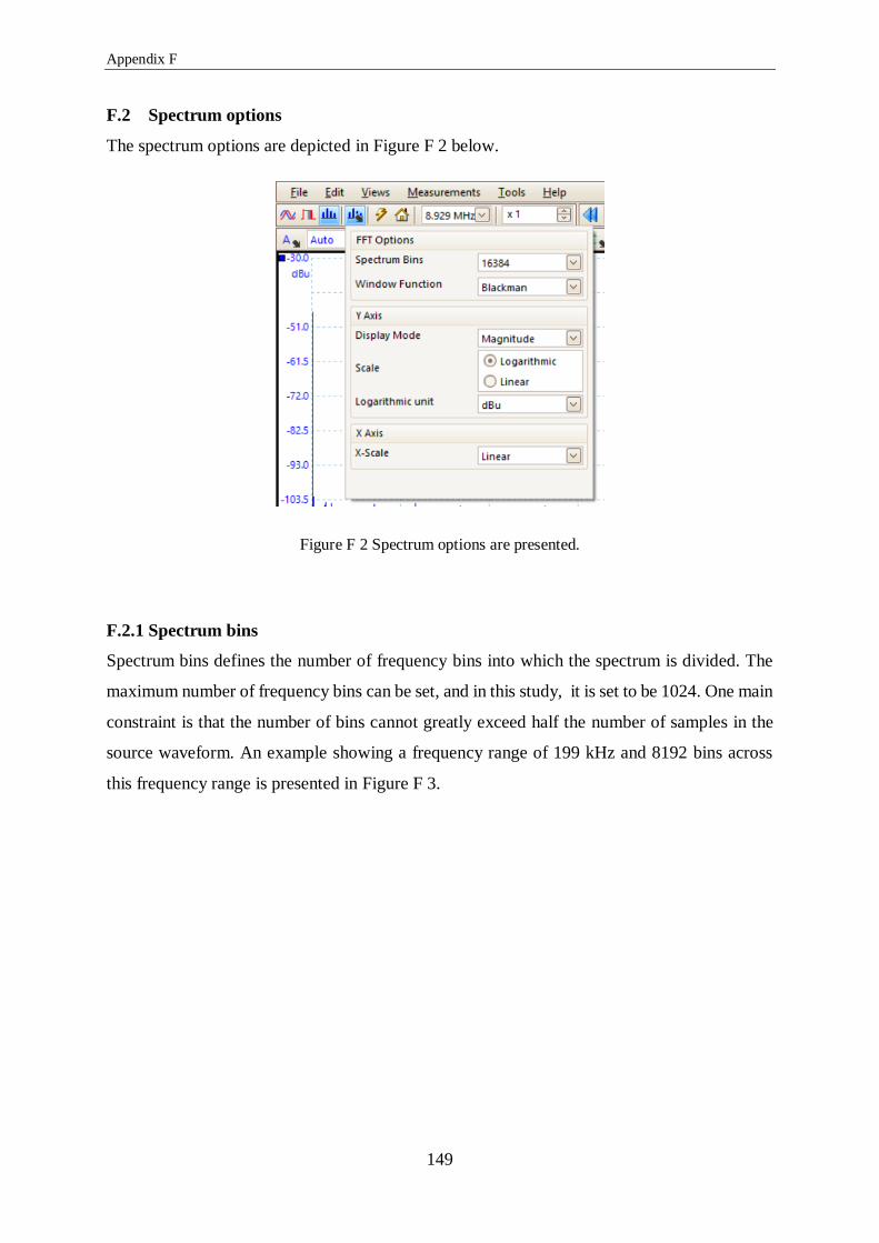
Appendix F
149
F.2 Spectrum options
The spectrum options are depicted in Figure F 2 below.
Figure F 2 Spectrum options are presented.
F.2.1 Spectrum bins
Spectrum bins defines the number of frequency bins into which the spectrum is divided. The
maximum number of frequency bins can be set, and in this study, it is set to be 1024. One main
constraint is that the number of bins cannot greatly exceed half the number of samples in the
source waveform. An example showing a frequency range of 199 kHz and 8192 bins across
this frequency range is presented in Figure F 3.

Appendix F
150
Figure F 3 An example of spectrum bins.
If the source waveform contains fewer samples than required (that is, fewer than twice the
number of frequency bins), Pico-Scope zero-pads the waveform up to the next power of two.
For example, if the scope view contains 10000 samples, Spectrum Bins is set to 16384, then
Pico-Scope zero-pads the waveform to 16384 samples, which is the nearest power of two
above 10000. It then uses these 16384 samples to provide 8192 frequency bins, not the
16 384 requested.
F.2.2 Window function
A number of standard window functions are available in Pico-scope. And a brief introduction
of each window function is presented in Table F1.
Table F 1 Window function in Pico-scope
Window
Main peak
width (bins
@ -3 dB)
Highest
side lobe
(dB)
Side lobe
roll-off
(dB/octave)
Notes
Blackman 1.68 -58 18 Often used for audio work.
Gaussian 1.33 to 1.79 -42 to -69 6 Gives minimal time and frequency
errors.
Triangular 1.28 -27 12 Also called Bartlett window.

Appendix F
151
Hamming 1.30 -41.9 6 Also called Raised sine squared.
Used in speech analysis.
Hann 1.20 to 1.86 -23 to -47 12 to 30 Also called sine squared. Used for
audio & vibration.
Blackman-
Harris 1.90 -92 6 General-purpose.
Flat-top 2.94 -44 6 Negligible pass-band ripple. Used
mainly for calibration.
Rectangular 0.89 -13.2 6 No fading. Maximal sharpness.
Used for short transients.
F.2.3 Display mode
There are three display modes available in spectrum mode: Magnitude, Average and Peak Hold.
a. Magnitude
In the Magnitude mode, the spectrum view shows the frequency spectrum of the last waveform
captured, whether live or stored in the waveform buffer. An example of Magnitude view is
presented in Figure F4.
Figure F 4 Example of Magnitude view of spectrum mode in Pico-scope.

Appendix F
152
b. Average
The spectrum view shows a rolling average of spectra calculated from all the waveforms in the
waveform. This has the effect of reducing the noise visible in the spectrum view. The Figure
below shows the noise floor being averaged of the above Magnitude view.
Figure F 5 Example of Average view of spectrum mode in Pico-scope.
c. Peak Hold
The spectrum view shows a rolling maximum of the spectra calculated from all the waveforms
in the buffer. In this mode, the amplitude of any frequency band in the spectrum view will
either stay the same or increase, but never decrease, over time. The Figure blow shows the
effects of peak hold on a waveform that is sweeping up and down in frequency from 1 kHz
to100 kHz.

Appendix F
153
Figure F 6 Example of Peak Hold view of spectrum mode in Pico-scope between 1 kHz and 100 kHz.
In this study, the Peak Hold view function is utilized to find frequency response of the VGSpeak.
F.2.4 Scales
a. Vertical Axis
The options of labelling and scaling of the vertical (signal) axis are listed in Table F2 below.
Table F 2 Labelling and scaling types of vertical axis in spectrum mode
Linear The vertical axis is scaled in volts.
Logarithmic The vertical axis is scaled in decibels, referred to the level selected below in
the Logarithmic unit control.
𝐝𝐁𝐕 Reference level is 1 volt.
𝒅𝑩𝒖 Reference level is 1 milliwatt with a load resistance of 600 ohms. This
corresponds to a voltage of about 775 mV.
𝐝𝐁𝐦 Reference level is one milliwatt into the specified load impedance. Enter the
load impedance in the box below the Logarithmic unit control.
Arbitrary
𝐝𝐁
Reference level is an arbitrary voltage, which you can specify in the box
below the Logarithmic unit control.

Appendix F
154
b. X Axis
The x axis can be set to either linear or log10 as shown in Figure F7 (a) and F7 (b) respectively.
(a) (b)
Figure F 7 X axis display modes: (a) linear mode; (b) log10 mode.
F.3 Conclusion
In this Appendix, the spectrum mode of the Pico-scope is briefly introduced including basic
controls, spectrum options, display mode and scales.
Reference
155
Reference
[1] D. J. Chamund, L. Coulbeck, D. R. Newcombe, and P. R. Waind, "High power density
IGBT module for high reliability applications," in 2009 IEEE 6th International Power
Electronics and Motion Control Conference, 2009, pp. 274-280.
[2] S. Yang, A. Bryant, P. Mawby, D. Xiang, L. Ran, and P. Tavner, "An industry-based
survey of reliability in power electronic converters," IEEE transactions on Industry
Applications, vol. 47, pp. 1441-1451, 2011.
[3] V. Smet, F. Forest, J.-J. Huselstein, F. Richardeau, Z. Khatir, S. Lefebvre, et al.,
"Ageing and failure modes of IGBT modules in high-temperature power cycling," IEEE
transactions on industrial electronics, vol. 58, pp. 4931-4941, 2011.
[4] Y. Shaoyong, X. Dawei, A. Bryant, P. Mawby, L. Ran, and P. Tavner, "Condition
monitoring for device reliability in power electronic converters: A review," Power
Electronics, IEEE Transactions on, vol. 25, pp. 2734-2752, 2010.
[5] O. Hyunseok, H. Bongtae, P. McCluskey, H. Changwoon, and B. D. Youn, "Physics-
of-failure, condition monitoring, and prognostics of insulated gate bipolar transistor
modules: A review," Power Electronics, IEEE Transactions on, vol. 30, pp. 2413-2426,
2015.
[6] K. L. Pandya and W. McDaniel, "A simplified method of generating thermal models
for power MOSFETs," in Semiconductor Thermal Measurement and Management,
2002. Eighteenth Annual IEEE Symposium, 2002, pp. 83-87.
[7] N. Baker, M. Liserre, L. Dupont, and Y. Avenas, "Improved reliability of power
modules: A review of online junction temperature measurement methods," IEEE
Industrial Electronics Magazine, vol. 8, pp. 17-27, 2014.
[8] D. C. Katsis and J. D. van Wyk, "Void-induced thermal impedance in power
semiconductor modules: Some transient temperature effects," IEEE Transactions on
Industry Applications, vol. 39, pp. 1239-1246, 2003.
[9] U. Scheuermann and U. Hecht, "Power cycling lifetime of advanced power modules
for different temperature swings," PCIM Nuremberg, vol. 5964, 2002.
[10] E. R. Motto and J. F. Donlon, "IGBT module with user accessible on-chip current and
temperature sensors," in 12th Annu. IEEEAppl. Power Electron. Conf. Expo, Orlando,
FL, USA, 2012, pp. 176–181.
[11] B. Thollin, J.-C. Crébier, Y. Avenas, P.-O. Jeannin, Z. Khatir, and L. Dupont,
"Development and electrical characterization of a vertical electrical and thermal test
chip (VTTC)," in Energy Conversion Congress and Exposition (ECCE), 2011 IEEE,
2011, pp. 60-67.
[12] Y. Avenas, L. Dupont, and Z. Khatir, "Temperature Measurement of Power
Semiconductor Devices by Thermo-Sensitive Electrical Parameters-A Review," Power
Electronics, IEEE Transactions on, vol. 27, pp. 3081-3092, 2012.
[13] J. L. Hudgins, G. S. Simin, E. Santi, and M. A. Khan, "An assessment of wide bandgap
semiconductors for power devices," Power Electronics, IEEE Transactions on, vol. 18,
pp. 907-914, 2003.
[14] S. Dimitrijev and P. Jamet, "Advances in SiC power MOSFET technology,"
Microelectronics reliability, vol. 43, pp. 225-233, 2003.
[15] J. O. Gonzalez, O. Alatise, J. Hu, L. Ran, and P. A. Mawby, "An Investigation of
Temperature-Sensitive Electrical Parameters for SiC Power MOSFETs," Ieee
Transactions on Power Electronics, vol. 32, pp. 7954-7966, Oct 2017.
[16] Wolfspeed. (Nov. 2015). C2M0080120D Silicon Carbide Power MOSFET Z-FETTM
MOSFET [Online].
Reference
156
[17] R. Pittini, Z. Zhe, and M. A. Andersen, "Switching performance evaluation of
commercial SiC power devices (SiC JFET and SiC MOSFET) in relation to the gate
driver complexity," in ECCE Asia Downunder (ECCE Asia), 2013 IEEE, 2013, pp.
233-239.
[18] J. Millan, P. Godignon, X. Perpina, A. Perez-Tomas, and J. Rebollo, "A survey of wide
bandgap power semiconductor devices," Power Electronics, IEEE Transactions on, vol.
29, pp. 2155-2163, 2014.
[19] W. Zhang, X. Huang, Z. Liu, F. C. Lee, S. She, W. Du, et al., "A new package of high-
voltage cascodegallium nitridedevice for megahertz operation," Power Electronics,
IEEE Transactions on, vol. PP, pp. 1-1, 2015.
[20] Wolfspeed. (2012). CMF20120D-Silicon Carbide Power MOSFET [Online]. Available:
https://www.wolfspeed.com/c2m0080120d?gclid=EAIaIQobChMI9LaYxdHs5QIVy7
HtCh1b-QsfEAAYAiAAEgJALvD_BwE
[21] R. Semiconductor. (Oct 2015). SCTMU001F. [Online]. Available:
https://www.rohm.com/products/sic-power-devices/sic-mosfet
[22] POWEREX. (2015). SiC MOSFET Modules. [Online]. Available:
https://www.pwrx.com/summary/SiC-Modules.aspx?c=55
[23] R. A. Wood and T. E. Salem, "Evaluation of a 1200-V, 800-A all-SiC dual module,"
IEEE Transactions on Power Electronics, vol. 26, pp. 2504-2511, 2011.
[24] J. Jordan, V. Esteve, E. Sanchis-Kilders, E. J. Dede, E. Maset, J. B. Ejea, et al., "A
comparative performance study of a 1200 v si and sic mosfet intrinsic diode on an
induction heating inverter," Power Electronics, IEEE Transactions on, vol. 29, pp.
2550-2562, 2014.
[25] S. M. Sze and K. K. Ng, Physics of semiconductor devices: John wiley & sons, 2006.
[26] D. A. Neamen, Semiconductor physics and devices vol. 3: McGraw-Hill New York,
1997.
[27] J. Lutz, H. Schlangenotto, U. Scheuermann, and R. De Doncker, Semiconductor power
devices: physics, characteristics, reliability: Springer Science & Business Media, 2011.
[28] S. Sorkin and סלבה .ס, Point Defects, Lattice Structure and Melting: Technion-Israel
Institute of Technology, Faculty of Physics, 2003.
[29] C. Zheng, Y. Yiying, D. Boroyevich, K. D. T. Ngo, P. Mattavelli, and K. Rajashekara,
"A 1200-V, 60-A SiC MOSFET multichip phase-Leg module for high-temperature,
high-frequency applications," Power Electronics, IEEE Transactions on, vol. 29, pp.
2307-2320, 2014.
[30] W. Zhiqiang, S. Xiaojie, L. M. Tolbert, F. F. Wang, L. Zhenxian, D. Costinett, et al.,
"A high temperature silicon carbide mosfet power module with integrated silicon-on-
insulator-based gate drive," Power Electronics, IEEE Transactions on, vol. 30, pp.
1432-1445, 2015.
[31] C. M. DiMarino, "High temperature characterization and analysis of silicon carbide
(SiC) power semiconductor transistors," Virginia Tech, 2014.
[32] J. L. e. al., "Validation and application of different experimental techniques to measure
electronic component operating junction temperature," IEEE Trans. Compon. Package
Technol, vol. 22, pp. 252–258, Jun. 1999.
[33] L. Dupont, Y. Avenas, and P. O. Jeannin, "Comparison of Junction Temperature
Evaluations in a Power IGBT Module Using an IR Camera and Three Thermosensitive
Electrical Parameters," Industry Applications, IEEE Transactions on, vol. 49, pp. 1599-
1608, 2013.
[34] D. L. Blackburn, "Temperature measurements of semiconductor devices-A review," in
Semiconductor Thermal Measurement and Management Symposium, 2004. Twentieth
Annual IEEE, 2004, pp. 70-80.
Reference
157
[35] K. Li, G. Y. Tian, L. Cheng, A. Yin, W. Cao, and S. Crichton, "State Detection of Bond
Wires in IGBT Modules Using Eddy Current Pulsed Thermography," IEEE
Transactions on Power Electronics, vol. 29, pp. 5000-5009, 2014.
[36] H. D. Z. Qi, Y. Wang, and J. W. Relf, "Thermal management of MOSFET junction
temperature in RF amplifier," presented at the Proc. 27th Annu. IEEE Semicond. Therm.
Meas.Manage. Symp, San Jose, CA, USA, 2011.
[37] M. H. T. Zhou, and B. Elison, "A quick method for estimation junction temperature
profiles in transient applications," presented at the Proc. Inter-Soc. Conf.Therm.
Phenonmena Electron. Syst, Orlando, FL, USA, 1996.
[38] D. L.Blackbum, "Temperature measurements of semiconductor devices—A reivew,"
presented at the 20th Annu. IEEE Semicond. Therm. Meas. Manage.Symp, San Jose,
CA, USA, 2004.
[39] Y. Xiong, X. Cheng, Z. J. Shen, C. Mi, H. Wu, and V. K. Garg, "Prognostic and warning
system for power-electronic modules in electric, hybrid electric, and fuel-cell vehicles,"
IEEE Transactions on Industrial Electronics, vol. 55, pp. 2268-2276, 2008.
[40] R. Matthe, H.-J. Humbert, and K. Kowalczyk, "Cell temperature and degradation
measurement in lithium ion battery systems using cell voltage and pack current
measurement and the relation of cell impedance to temperature based on signal given
by the power inverter," ed: Google Patents, 2015.
[41] K. Wang, Y. Liao, G. Song, and X. Ma, "Over-Temperature protection for IGBT
modules," in PCIM Europe 2014; International Exhibition and Conference for Power
Electronics, Intelligent Motion, Renewable Energy and Energy Management;
Proceedings of, 2014, pp. 1-7.
[42] S. D. R.C.S. Freire, and G.S. Deep, "A p-n junction temperature sensor with switched
current excitation," in IEEE Instrum. Meas.Technol. Conf, Irvine, CA, USA, 1993, pp.
310–315.
[43] N. Iwamuro, Y. Harada, T. Yamazaki, N. Kumagai, and Y. Seki, "A New Vertical Igbt
Structure with a Monolithic over-Current, over-Voltage, and over-Temperature Sensing
and Protecting Circuit," Ieee Electron Device Letters, vol. 16, pp. 399-401, Sep 1995.
[44] R. C. S. Freire, S. Daher, and G. S. Deep, "A Highly Linear Single P-N-Junction
Temperature Sensor," Ieee Transactions on Instrumentation and Measurement, vol. 43,
pp. 127-132, Apr 1994.
[45] T. Kajiwara, A. Yamagaguchi, Y. Hoshi, K. Sakurai, and J. Gallagher, "New intelligent
power multi-chips modules with junction temperature detecting function," in IEEE Ind.
Appl. Conf, St. Louis, MO, USA, 1993, pp. 1085–1090.
[46] M. Berthou, P. Godignon, and J. Millán, "Monolithically Integrated Temperature
Sensor in Silicon Carbide Power MOSFETs," IEEE Transactions on Power Electronics,
vol. 29, pp. 4970-4977, 2014.
[47] C. Yao, P. Yang, M. Leng, H. Li, L. Fu, J. Wang, et al., "Electromagnetic noise
coupling and mitigation for fast response on-die temperature sensing in high power
modules," in Applied Power Electronics Conference and Exposition (APEC), 2016
IEEE, 2016, pp. 1554-1560.
[48] X. Kun, F. C. Lee, and D. Boroyevich, "Extraction of parasitics within wire-bond IGBT
modules," in 13 Annu. Appl. Power Electron. Conf. Expo, Anaheim, CA, USA, 1998,
pp. 497-503.
[49] W. Brekel, T. Duetemeyer, G. Puk, and O. Schilling, "Time resolved in situ Tvj
measurements of 6.5kV IGBTs during inverter operation," in PCIM Europe, 2009, pp.
808–813.
[50] N. Baker, S. Munk-Nielsen, M. Liserre, and F. Iannuzzo, "Online junction temperature
measurement via internal gate resistance during turn-on," in Power Electronics and

Reference
158
Applications (EPE'14-ECCE Europe), 2014 16th European Conference on, 2014, pp.
1-10.
[51] C. Z. Lu, M. Z.Wang, X. Gui, G. B. Gao, and B. J. Yi, "Fast measurement of the peak
junction temperature of power transistors using electrical method," in IEEE 7th Annu.
Semicond. Therm. Meas. Manage. Symp, Phoenix, AZ, USA, 1991, pp. 39-43.
[52] J. L. Barnette, "Lifetime synchronization of parallel DC/DC converters," M.S., North
Carolina A&D Univ, Greensboro, NC, USA, 2006.
[53] A. Koenig, T. Plum, P. Fidler, and R. W. De Doncker, "On-line Junction Temperature
Measurement of CoolMOS Devices," in Power Electronics and Drive Systems, 2007.
PEDS '07. 7th International Conference on, 2007, pp. 90-95.
[54] Y. S. Kim and S. K. Sul, "On-line estimation of IGBT junction temperature using on-
state voltage drop," in 33rd Ind. Appl. Conf, St. Louis, MO, USA, 1998, pp. 853-859.
[55] P. Ghimire, A. R. d. Vega, S. Beczkowski, S. Munk-Nielsen, and B. Rannested, "An
online Vce measurement and temperature estimation method for high power IGBT
module in normal PWM operation," in Int. Power Electron. Conf, Hiroshima, Japan,
2014, pp. 2850–2855.
[56] R. Schmidt and U. Scheuermann, "Using the chip as a temperature sensor—The
influence of steep lateral temperature gradient on the Vce(T) measurement," in Eur.
Conf. Power Electron. Appl, Barcelona, Italy, 2009, pp. 1-9.
[57] X. Jorda, X. Perpina, M. Vellvehi, and J. Coleto, "Power-Substrate Static Thermal
Characterization Based on a Test Chip," Ieee Transactions on Device and Materials
Reliability, vol. 8, pp. 671-679, Dec 2008.
[58] P. Ghimire, K. B. Pedersen, I. Trintis, B. Rannestad, and S. Munk-Nielsen, "Online
chip temperature monitoring using υce-load current and IR thermography," in IEEE
Energy Convers. Congr. Expo, Montreal, QC, Canada, 2015, pp. 6602–6609.
[59] L. Dupont and Y. Avenas, "Preliminary Evaluation of Thermo-Sensitive Electrical
Parameters Based on the Forward Voltage for Online Chip Temperature Measurements
of IGBT Devices," Ieee Transactions on Industry Applications, vol. 51, pp. 4688-4698,
Nov-Dec 2015.
[60] N. Baker, M. Liserre, L. Dupont, and Y. Avenas, "Improved Reliability of Power
Modules A Review of Online Junction Temperature Measurement Methods," Ieee
Industrial Electronics Magazine, vol. 8, pp. 17-27, Sep 2014.
[61] V. Sundaramoorthy, E. Bianda, R. Bloch, I. Nistor, G. Knapp, and A. Heinemann,
"Online estimation of IGBT junction temperature (Tj) using gate-emitter voltage (Vge)
at turn-off," in Power Electronics and Applications (EPE), 2013 15th European
Conference on, 2013, pp. 1-10.
[62] P. S. e. al, "Online junction temperature extraction with turn-off delay time for high
power IGBTs," in Energy Convers. Congr. Expo, Pittsburgh, PA, USA, 2014, pp.
4016–4021., 2014.
[63] I. Bahun, N. Cobanov, and Z. Jakopovic, "Real-Time Measurement of IGBT's
Operating Temperature," Automatika, vol. 52, pp. 295-305, Nov-Dec 2011.
[64] M. M. e. al, "Temperature dependence of switching performance in IGBT circuits and
its compact modeling," in 23rd Int. Symp. Power Semicond. Devices ICs, 2011, pp.
148–151.
[65] A. Haertl, G. Soelkner, F. Pfirsch, W. Brekel, and T. Duetemeyer, "Influence of
dynamic switching on the robustness of power devices against cosmic radiation," in
24th Int. Symp. Power Semicond. Devices ICs, 2012, pp. 353–356.
[66] A. Bryant, Y. Shaoyong, P. Mawby, X. Dawei, L. Ran, P. Tavner, et al., "Investigation
Into IGBT dV/dt During Turn-Off and Its Temperature Dependence," Power
Electronics, IEEE Transactions on, vol. 26, pp. 3019-3031, 2011.

Reference
159
[67] H. Z. Luo, Y. X. Chen, P. F. Sun, W. H. Li, and X. N. He, "Junction Temperature
Extraction Approach With Turn-Off Delay Time for High-Voltage High-Power IGBT
Modules," Ieee Transactions on Power Electronics, vol. 31, pp. 5122-5132, Jul 2016.
[68] Z. Xu, F.Wang, and P.Ning, "Junction temperature measurement of IGBTs using short
circuit current," in IEEE Energy Convers. Congr. Expo, Raleigh, NC, USA, 2012, pp.
91-96.
[69] V. K. Sundaramoorthy, E. Bianda, R. Bloch, and F. Zurfluh, "Simultaneous online
estimation of junction temperature and current of IGBTs using emitter-auxiliary emitter
parasitic inductance," in PCIM Europe 2014; International Exhibition and Conference
for Power Electronics, Intelligent Motion, Renewable Energy and Energy Management,
2014, pp. 1-8.
[70] H. Chen, V. Pickert, D. J. Atkinson, and L. S. Pritchard, "On-line Monitoring of the
MOSFET Device Junction Temperature by Computation of the Threshold Voltage," in
Power Electronics, Machines and Drives, 2006. The 3rd IET International Conference
on, 2006, pp. 440-444.
[71] H. Niu and R. D. Lorenz, "Sensing power MOSFET junction temperature using gate
drive turn-on current transient properties," in IEEE Energy Convers. Congr. Expo,
Pittsburgh, PA, USA, 2014, pp. 2909–2916.
[72] H. Niu and R. D. Lorenz, "Sensing IGBT junction temperature using gate drive output
transient properties," in Applied Power Electronics Conference and Exposition (APEC),
2015 IEEE, 2015, pp. 2492-2499.
[73] H. Niu and R. D. Lorenz, "Sensing gallium nitride HEMT junction temperature using
gate drive output transient properties," in IEEE Appl. Power Electron. Conf. Expo,
Long Beach, CA, USA, 2015, pp. 2792–2499.
[74] Z. Pan, "A quick method for estimation junction temperature profiles in transient
applications," in Power Electron. Motion Control Conf, Beijing, China, 2000, pp.
1068–1073.
[75] M. H. Bierhoff and F. W. Fuchs, "Semiconductor losses in voltage source and current
source IGBT converters based on analytical derivation," in IEEE 35th Power Electron.
Spec. Conf, Aachen, Germany, 2004, pp. 2836–2842.
[76] Q. Tu and Z. Xu, "Power losses evaluation for modular multilevel converter with
junction temperature feedback," in 2011 IEEE Power and Energy Society General
Meeting, 2011, pp. 1-7.
[77] M. Musallam, P. Acarnley, M. Johnson, and L. Pritchard, "Real-time power electronic
device junction temperature estimation," in 2nd Int. Conf. Power Electron., Mach.
Drives, Edinburgh, U.K, 2004, pp. 231-235.
[78] D. Andler, E. Hauk, R. A. lvarez, J. Weber, S. Bernet, and J. Rodr´ıguez, "New junction
temperature balancing method for a three level active NPC converter," in 14th Eur.
Conf. Power Electron. Appl, Birmingham, U.K, 2011, pp. 1-9.
[79] D. A. Murdock, J. E. R. Torres, J. J. Connors, and R. D. Lorenz, "Active thermal control
of power electronic modules," Ieee Transactions on Industry Applications, vol. 42, pp.
552-558, Mar-Apr 2006.
[80] Z. Wang, W. Qiao, and L. Qu, "Frequency domain transient temperature estimation and
aging analysis for weak points of IGBT modules," in IEEE Energy Convers. Congr.
Expo, Pittsburgh, PA, USA, 2014, pp. 4036–4042.
[81] V. Smet, "Ageing and failure modes of IGBT modules in hightemperature power
cycling," IEEE Trans. Ind. Appl, vol. 58, pp. 4931–4941, Feb. 2011.
[82] N. Baker, L. Dupont, S. Munk-Nielsen, F. Iannuzzo, and M. Liserre, "IR Camera
Validation of IGBT Junction Temperature Measurement via Peak Gate Current," IEEE
Transactions on Power Electronics, vol. 32, pp. 3099-3111, 2017.
Reference
160
[83] I. Cree, "C2M0080120D Silicon Carbide Power Mosfet Datasheet," ed: Durham, 2014.
[84] S. E. Laux, "Techniques for small-signal analysis of semiconductor devices," IEEE
Transactions on Electron Devices, vol. 32, pp. 2028-2037, 1985.
[85] J. Huang, K. A. Corzine, and M. Belkhayat, "Small-signal impedance measurement of
power-electronics-based AC power systems using line-to-line current injection," IEEE
Transactions on Power Electronics, vol. 24, pp. 445-455, 2009.
[86] B. Miao, R. Zane, and D. Maksimovic, "System identification of power converters with
digital control through cross-correlation methods," IEEE Transactions on Power
Electronics, vol. 20, pp. 1093-1099, 2005.
[87] C. Chen, L. Li, Q. Zhang, Q. Tong, K. Liu, D. Lyu, et al., "Online Inductor Parameters
Identification by Small-Signal Injection for Sensorless Predictive Current Controlled
Boost Converter," IEEE Transactions on Industrial Informatics, vol. 13, pp. 1554-1564,
2017.
[88] M. Mudholkar, S. Ahmed, M. N. Ericson, S. S. Frank, C. L. Britton, and H. A. Mantooth,
"Datasheet Driven Silicon Carbide Power MOSFET Model," Power Electronics, IEEE
Transactions on, vol. 29, pp. 2220-2228, 2014.
[89] Z. Bin, Q. Haihong, N. Xin, and Y. Yangguang, "Evaluation of isolated gate driver for
SiC MOSFETs," in Industrial Electronics and Applications (ICIEA), 2013 8th IEEE
Conference on, 2013, pp. 1208-1212.
[90] M. Engelhardt, "Ltspice iv," Linear Technology Corporation, Sept, 2011.
[91] Coilcraft. (2017). PWB1010-1LC Wide-band RF transformer 1:1 0.03-250 MHz
datasheet [Online].
[92] Cree/Wolfspeed. (2012). KIT8020CRD8FF1217P-1 CREE Silicon Carbide MOSFET
Evaluation Kit [Online].
[93] H. Kuhn and A. Mertens, "On-line junction temperature measurement of IGBTs based
on temperature sensitive electrical parameters," in Power Electronics and Applications,
2009. EPE '09. 13th European Conference on, 2009, pp. 1-10.
[94] E. Wolfgang, "Examples for failures in power electronics systems," ECPE tutorial on
reliability of power electronic systems, Nuremberg, Germany, pp. 19-20, 2007.
[95] M. Mermet-Guyennet, "Reliability requirement for traction power converters,"
ECPEWorkshop ‘Built-in Rel. Power Electron. Syst.’Toulouse, France, 2008.
[96] Y. Han and Y. H. Song, "Condition monitoring techniques for electrical equipment-a
literature survey," IEEE Transactions on Power delivery, vol. 18, pp. 4-13, 2003.
[97] R. Bayerer, "Higher Junction Temperature in Power Modules–a demand from hybrid
cars, a potential for the next step increase in power density for various Variable Speed
Drives," Power Conversion Intelligent Motion, 2008.
[98] Y. Avenas, L. Dupont, and Z. Khatir, "Temperature measurement of power
semiconductor devices by thermo-sensitive electrical parameters—A review," Power
Electronics, IEEE Transactions on, vol. 27, pp. 3081-3092, 2012.
[99] N. Patil, D. Das, K. Goebel, and M. Pecht, "Identification of failure precursor
parameters for insulated gate bipolar transistors (IGBTs)," in Prognostics and Health
Management, 2008. PHM 2008. International Conference on, 2008, pp. 1-5.
[100] B. J. Baliga, "Temperature behavior of insulated gate transistor characteristics," Solid-
state electronics, vol. 28, pp. 289-297, 1985.
[101] B. Wang, Y. Tang, and M. Chen, "Study on Electric Characteristic of IGBT at Different
Junction Temperature," in Power and Energy Engineering Conference (APPEEC),
2011 Asia-Pacific, 2011, pp. 1-4.
[102] N. Patil, J. Celaya, D. Das, K. Goebel, and M. Pecht, "Precursor parameter
identification for insulated gate bipolar transistor (IGBT) prognostics," IEEE
Transactions on Reliability, vol. 58, pp. 271-276, 2009.

Reference
161
[103] M. Held, P. Jacob, G. Nicoletti, P. Scacco And, and M. H. Poech, "Fast power cycling
test for insulated gate bipolar transistor modules in traction application," International
journal of electronics, vol. 86, pp. 1193-1204, 1999.
[104] G. Lefranc, T. Licht, H. J. Schultz, R. Beinert, and G. Mitic, "Reliability testing of high-
power multi-chip IGBT modules," Microelectronics reliability, vol. 40, pp. 1659-1663,
2000.
[105] C. Kainan, Z. Zhengming, Y. Liqiang, L. Ting, and H. Fanbo, "The Impact of Nonlinear
Junction Capacitance on Switching Transient and Its Modeling for SiC MOSFET,"
Electron Devices, IEEE Transactions on, vol. 62, pp. 333-338, 2015.
[106] H. Kuhn and A. Mertens, "On-line junction temperature measurement of IGBTs based
on temperature sensitive electrical parameters," in Power Electronics and Applications,
2009. EPE'09. 13th European Conference on, 2009, pp. 1-10.
[107] P. O'Connor and A. Kleyner, Practical reliability engineering: John Wiley & Sons,
2012.
[108] A. Bryant, S. Yang, P. Mawby, D. Xiang, L. Ran, P. Tavner, et al., "Investigation into
IGBT dV/dt during turn-off and its temperature dependence," Power Electronics, IEEE
Transactions on, vol. 26, pp. 3019-3031, 2011.
[109] M. Pecht and J. Cu, "Physics-of-failure-based prognostics for electronic products,"
Transactions of the Institute of Measurement and Control, vol. 31, pp. 309-322, Jun-
Aug 2009.
[110] International Rectifier Application. (2015). Note AN- 983: IGBT Characteristics.
[Online]. Available: http://www.irf.com/part/600V-COPACK-IGBT-IN-A-TO-
220AB-PACKAGE/_/A~IRG7IC23FD
[111] D. L. Goodman, "Prognostic methodology for deep submicron semiconductor failure
modes," IEEE Transactions on Components and Packaging Technologies, vol. 24, pp.
109-111, 2001.
[112] B. Tian, W. Qiao, Z. Wang, T. Gachovska, and J. L. Hudgins, "Monitoring IGBT's
health condition via junction temperature variations," in Applied Power Electronics
Conference and Exposition (APEC), 2014 Twenty-Ninth Annual IEEE, 2014, pp. 2550-
2555.
[113] H. Niu and R. D. Lorenz, "Real-Time Junction Temperature Sensing for Silicon
Carbide MOSFET With Different Gate Drive Topologies and Different Operating
Conditions," IEEE Transactions on Power Electronics, vol. 33, pp. 3424-3440, 2018.
[114] L. Shu, J. Zhang, F. Peng, and Z. Chen, "A voltage controlled current source gate drive
method for IGBT devices," in Energy Conversion Congress and Exposition (ECCE),
2014 IEEE, 2014, pp. 5525-5530.
[115] M. H. Rashid, Power electronics handbook: Butterworth-Heinemann, 2017.
[116] G. Wang, X. Huang, J. Wang, T. Zhao, S. Bhattacharya, and A. Q. Huang,
"Comparisons of 6.5 kV 25A Si IGBT and 10-kV SiC MOSFET in solid-state
transformer application," in Energy Conversion Congress and Exposition (ECCE),
2010 IEEE, 2010, pp. 100-104.
[117] W. Jun, Z. Tiefu, L. Jun, A. Q. Huang, R. Callanan, F. Husna, et al., "Characterization,
Modeling, and Application of 10-kV SiC MOSFET," Electron Devices, IEEE
Transactions on, vol. 55, pp. 1798-1806, 2008.
[118] T. Zhao, J. Wang, A. Q. Huang, and A. Agarwal, "Comparisons of SiC MOSFET and
Si IGBT based motor drive systems," in Industry Applications Conference, 2007. 42nd
IAS Annual Meeting. Conference Record of the 2007 IEEE, 2007, pp. 331-335.
[119] A. Ong, J. Carr, J. Balda, and A. Mantooth, "A comparison of silicon and silicon carbide
MOSFET switching characteristics," in Region 5 Technical Conference, 2007 IEEE,
2007, pp. 273-277.

Reference
162
[120] E. Wilson, "MOSFET current source gate drivers, switching loss modeling and
frequency dithering control for MHz switching frequency DC–DC converters,"
Queen’s University Kingston, Ontario, Canada, 2008.
[121] Cree.(2015). SiC MOSFET isolated gate driver. [ONLINE]. Available:
http://www.wolfspeed.com/downloads/dl/file/id/572/product/199/crd_001.pdf.

Reference
163