
On-wafer Electrical Characterization of Silicon Carbide (SiC ...
119
ΠΟΛΥΤΕΧΝΕΙΟ ΚΡΗΤΗΣ ΣΧΟΛΗ ΗΛΕΚΤΡΟΝΙΚΩΝ ΜΗΧΑΝΙΚΩΝ ΚΑΙ ΜΗΧΑΝΙΚΩΝ ΥΠΟΛΟΓΙΣΤΩΝ ΤΟΜΕΑΣ ΗΛΕΚΤΡΟΝΙΚΗΣ ΚΑΙ ΑΡΧΙΤΕΚΤΟΝΙΚΗΣ ΥΠΟΛΟΓΙΣΤΩΝ On-wafer Electrical Characterization of Silicon Carbide (SiC) JFETs ΜΕΤΑΠΤΥΧΙΑΚΗ ΔΙΑΤΡΙΒΗ BΑΜΒΟΥΚΑΚΗΣ Ι. ΚΩΝΣΤΑΝΤΙΝΟΣ Επιβλέπων: Bucher Matthias Αναπληρωτής Καθηγητής Π.Κ. Χανιά, Απρίλιος 2016
-
Upload
khangminh22 -
Category
Documents
-
view
2 -
download
0
Transcript of On-wafer Electrical Characterization of Silicon Carbide (SiC ...

ΠΟΛΥΤΕΧΝΕΙΟ ΚΡΗΤΗΣ
ΣΧΟΛΗ ΗΛΕΚΤΡΟΝΙΚΩΝ
ΜΗΧΑΝΙΚΩΝ ΚΑΙ ΜΗΧΑΝΙΚΩΝ
ΥΠΟΛΟΓΙΣΤΩΝ
ΤΟΜΕΑΣ ΗΛΕΚΤΡΟΝΙΚΗΣ ΚΑΙ
ΑΡΧΙΤΕΚΤΟΝΙΚΗΣ ΥΠΟΛΟΓΙΣΤΩΝ
On-wafer Electrical Characterization
of Silicon Carbide (SiC) JFETs
ΜΕΤΑΠΤΥΧΙΑΚΗ ΔΙΑΤΡΙΒΗ
BΑΜΒΟΥΚΑΚΗΣ Ι. ΚΩΝΣΤΑΝΤΙΝΟΣ
Επιβλέπων: Bucher Matthias
Αναπληρωτής Καθηγητής Π.Κ.
Χανιά, Απρίλιος 2016

2

3
ΠΟΛΥΤΕΧΝΕΙΟ ΚΡΗΤΗΣ
ΣΧΟΛΗ ΗΛΕΚΤΡΟΝΙΚΩΝ
ΜΗΧΑΝΙΚΩΝ ΚΑΙ ΜΗΧΑΝΙΚΩΝ
ΥΠΟΛΟΓΙΣΤΩΝ
ΤΟΜΕΑΣ ΗΛΕΚΤΡΟΝΙΚΗΣ ΚΑΙ
ΑΡΧΙΤΕΚΤΟΝΙΚΗΣ ΥΠΟΛΟΓΙΣΤΩΝ
On-wafer Electrical Characterization
of Silicon Carbide (SiC) JFETs
ΜΕΤΑΠΤΥΧΙΑΚΗ ΔΙΑΤΡΙΒΗ
BΑΜΒΟΥΚΑΚΗΣ Ι. ΚΩΝΣΤΑΝΤΙΝΟΣ
Εξεταστική Επιτροπή:
M. Bucher Κ. Ζεκεντές Γ. Σταυρακάκης Αναπληρωτής Καθηγητής Π.Κ. Ερευνητής Β’, ΙΤΕ Καθηγητής Π.Κ.
Χανιά, Απρίλιος 2016

4

5
KEY WORDS:
Silicon Carbide (SiC), Junction Field-Effect Transistor (JFET), Electrical
Characterization, I-V measurements, C-V measurements, MATLAB Simulations
ABSTRACT
Power electronics technologies are very important in electrical energy conversion systems, where
the power semiconductor devices play a crucial role. Power electronics technologies have developed
with silicon (Si) material which is approaching its theoretical limits. As a result, nowadays new wide
bandgap (WBG) semiconductor materials exhibit great interest and seem to be suitable for the next
generation power electronics applications.
Silicon Carbide (SiC) is a very promising WBG material with a set of superior properties,
including wide bandgap, high thermal conductivity, high critical electric field and high electron
mobility. This makes it an excellent material for electronic device applications that can operate
under high temperature and high power conditions. Our work was focused on the electrical
characterization of Junction Field-Effect Transistors (JFETs) and diodes fabricated with this material
at the premises of Microelectronics Research Group at IESL-FORTH. Many samples were
characterized which led to the extraction of useful results and conclusions about both the electrical
characterization procedure, and the design and fabrication process that has been followed. Detailed
information about the latter ones is provided in chapter 3. Hereby, the results from two samples are
reported as the measurements and the extraction procedure in their case, were systematic and can,
thus, give a comprehensive description of the subject.
In chapters 4 and 5 the electrical characterization procedure, including the different
measurements that need to be carried out and the corresponding experimental setups are described,
along with the results of the characterization of the two different samples. Moreover, in the last
chapter the agreement of the measured characteristics with the theoretically anticipated ones
according to the JFET theory, is investigated. There is comparison between some measured results
and the corresponding simulated. The theory for the JFET operation, is presented in chapter 2. It is
worthwhile to mention that for the simulations the MATLAB software was used.
In the Appendices, the reader can find a comprehensive report for the capacitance voltage-
measurements in FETs (Appendix 1) and a compact handbook including equations for the
calculation of critical JFET parameters (Appendix 2). Moreover, in Appendix 3, the MATLAB
scripts used for the simulations are presented.

6
ΠΡΟΛΟΓΟΣ
Η παρούσα διπλωματική εργασία εκπονήθηκε στον τομέα Hλεκτρονικής και Αρχιτεκτονικής
Υπολογιστών της Σχολής Ηλεκτρονικών Μηχανικών και Μηχανικών Υπολογιστών του
Πολυτεχνείου Κρήτης.
Υπεύθυνος κατά την εκπόνηση της διπλωματικής εργασίας ήταν ο Αναπληρωτής Καθηγητής
κύριος Μatthias Bucher στον οποίο οφείλω ιδιαίτερες ευχαριστίες αρχικά για την ανάθεσή της
καθώς και για την άψογη επιστημονική υποστήριξη και καθοδήγηση που μου προσέφερε.
Θερμές ευχαριστίες οφείλω στον κύριο Κωνσταντίνο Ζεκεντέ, Ερευνητή Β’ του Ιδρύματος
Τεχνολογίας και Έρευνας (ΙΤΕ) για την αμέριστη βοήθεια, την υποστήριξη και τις κατευθυντήριες
συμβουλές που μου παρείχε καθ’ όλη τη διάρκεια εκπόνησης της εργασίας. Ακόμα ευχαριστώ
ιδιαιτέρως τον συνάδελφο Ηλ. Μηχανικό Μ. Βασσάκη, τον υποψήφιο Διδάκτορα του Πολυτεχνείου
Κρήτης, Ν. Μακρή καθώς και την ομάδα Μικροηλεκρονικής (MRG) του ΙΗΔΛ-ΙΤΕ και ιδιαίτερα
την κυρία Μ. Καγιαμπάκη. Χωρίς τη πολύτιμη αρωγή και συνεισφορά όλων τους η εκπόνηση της
εργασίας αυτής δεν θα ήταν δυνατή.
Τέλος, θέλω να ευχαριστήσω την οικογένειά μου για την αμέριστη εμπιστοσύνη που ανέκαθεν
μου έδειχναν.
Χανιά, Απρίλιος 2016
Κωνσταντίνος Ι. Βαμβουκάκης

7

8
Contents
Chapter 1. Introduction ................................................................................................................. 10
1.1 WBG Semiconductor materials ............................................................................................ 10
1.2 SiC Power transistors ............................................................................................................ 12
1.3 Scope of the Dissertation – Outline ...................................................................................... 13
Chapter 2. Operation principle of JFETs ................................................................................... 16
2.1 Introduction – Principle of JFET operation .......................................................................... 16
2.2 Analytical Description of VJFET Operation ........................................................................ 21
2.2.1 Forward Conduction Operation ..................................................................................... 21
2.2.2 Forward blocking operation ........................................................................................... 24
2.2.3 Capacitance model ......................................................................................................... 29
Chapter 3. Design and fabrication process of investigated samples .......................................... 30
3.1 Quality of SiC wafer ............................................................................................................. 30
3.2 Dimensions and geometries .................................................................................................. 31
3.3 Fabrication of the transistors ................................................................................................. 32
3.3.1 Transistor sample structure ............................................................................................ 32
3.3.2 Transistor fabrication ..................................................................................................... 33
Chapter 4. JFET Electrical characterization procedure-Measurement results from sample
CB145602-P1 ..................................................................................................................................... 37
4.1 Transistor geometry determination. ...................................................................................... 37
4.2 Theoretical values estimation of parameters ......................................................................... 40
4.3 First run of measurements in one mask period ..................................................................... 42
4.4 Measurements in different mask periods – Statistical study ................................................. 50
4.5 Measurements of best devices .............................................................................................. 56
4.6 Specifications tables ............................................................................................................. 66
4.7 Conclusions ........................................................................................................................... 71
Chapter 5. Measurement results from sample CB145602-P4 .................................................... 72
5.1 Transistor geometry determination. ...................................................................................... 72
5.2 Theoretical values estimation of parameters ......................................................................... 74
5.3 First run of measurements in one mask period ..................................................................... 75
5.4 Measurements in different mask periods – Statistical study ................................................. 76
5.5 Measurements of best devices .............................................................................................. 79
5.6 Specifications tables ............................................................................................................. 83
5.7 Conclusions ........................................................................................................................... 88
Chapter 6. Comparisons between measuremenets and Simulations ......................................... 89
6.1 Introduction ........................................................................................................................... 89
6.2 Comparisons ......................................................................................................................... 90
Chapter 7. Summary, Conclusions and Suggestions .................................................................. 92

9
7.1 Summary and conclusions .................................................................................................... 92
7.2 Suggestions and future work ................................................................................................. 93
Appendices ..................................................................................................................................... 95
Appendix 1. FET Capacitance Voltage measurements procedure .................................................. 95
Appendix 2. Theoretical VJFET Analysis Handbook .................................................................. 108
Appendix 3. Simulation files-MATLAB Code ............................................................................. 112
Publications: ................................................................................................................................ 116
References: ................................................................................................................................... 117

10
Chapter 1. Introduction
1.1 WBG Semiconductor materials
Power electronics technologies are very important in electrical energy conversion systems, where
the power semiconductor devices play an crucial role. Some of the potential application areas for
these WBG devices include: transportation electrification and renewable energy. Regarding
renewable energy which is a major trend today, wide bandgap devices have been explored for
replacement of Si insulated gate bipolar transistors (IGBTs) in photovoltaic inverters in order to
improve efficiency. WBG semiconductors are well suited for these applications due to their high
temperature capabilities, fast switching speeds, and low losses. The high temperature capability of
these devices allow them to better withstand the harsh environmental conditions, and have relaxed
cooling system requirements. In addition to this high temperature capability, the fast switching speed
of these devices allows for higher frequency operation thereby resulting in the reduction of the
passive components, which decreases the total size, weight, and cost of the system.
Since the birth of the first power transistor in 1947, power electronics technologies have
developed with silicon (Si) material. Up until today, with the development of more than 60 years, Si
power semiconductor devices fabrication process is very mature and can meet different power
demands in electrical energy conversion [10]. However, compared to Si, wide bandgap (WBG)
semiconductor materials have lots of advantages which are very attractive for new power electronics
applications. As silicon devices are approaching its theoretical limits, wide bandgap semiconductors
are naturally suitable for the next generation power electronics applications. Even though they are
not yet challenging silicon’s existing dominance in this market, their increasingly maturing
technology is expected to lead to great commercialization success in the years to come. While SiC
has been identified as a very promising material for power electronics applications, the high-
performance devices based on SiC cannot become true unless a broad range of device fabrication
technology has been developed for this material. During the last twenty years, a substantial amount
of efforts have been spent on the research and experimental development of SiC processing
technologies. Fortunately, most of the general microelectronic techniques developed by the silicon
industry can be directly applied to SiC device fabrication with little or minor modification.
Furthermore, specialized process technologies for SiC etching, selective doping and dopant
activation, ohmic and Schottky contact structures, etc. have also been well developed.
Table 1.1: Properties of important semiconductor materials. [13]

11
A comparison of some material properties of several important semiconductors is listed in Table
1.1 above. The energy bandgap Eg between conduction band and valance band is 1.12eV for Si,
while that for SiC, GaN and Diamond is 3.26eV, 3.39eV and 5.45eV respectively. A big value of Eg
means that an electron is less possible to go through this band when temperature increases, allowing
higher maximum operating temperature values. In terms of thermal conductivity, SiC and Diamond
are much greater than Si, which means that they can transfer heat easily thus higher current densities
are anticipated for SiC power devices. It is also observed that WBG materials have smaller relative
permittivity εr and bigger saturation velocity vsat than Si. Thus, smaller εr helps to realize power
semiconductor devices with smaller inter-electrode capacitances, thereby to increase fast switching
abilities. For the critical breakdown field Ec, there are much bigger values for WBG materials than
Si, which indicates that for the materials with the same thickness, there are much bigger breaking
voltages for WBG materials than Si.
To sum up, SiC, the material that our work is focused on, when compared to silicon, has three
times wider bandgap (Eg), ten times higher critical electric field (Ec), nineteen orders of magnitude
lower intrinsic carrier concentration (ni), three times larger thermal conductivity (λ) and two times
higher saturation velocity (vsat). These characteristics show great potential to make power devices
that can operate at higher power, higher temperature and higher frequency with lower leakage
current, smaller conduction and switching losses, less stringent requirements in heat removal. From
the three SiC polytypes 3C, 4H and 6H, 4H-SiC seems to be the most interesting one for the time
being [13].
A quite descriptive figure for the properties of SiC follows. Properties of Silicon and GaN are
also presented for comparison.
Fig. 1.1: Graphical representation of SiC, GaN and Si properties [14].
Moreover from the Table 1.1, it can be seen that diamond is an excellent candidate for power
semiconductor devices, however, due to the complexity in the fabrication process, diamond power
devices are not for the time being commercially available but intensive research is underway towards
to the fabrication of diamond power devices.

12
1.2 SiC Power transistors
Silicon Carbide (SiC) is one of the earliest few materials that are recognized as semiconductors.
Although SiC was named “the perfect semiconductor” by William Shockley back in 1950s, the
difficulties of growing large size single crystals of SiC seriously delayed the development of SiC
electronics with the first commercially available 2-inch SiC wafers introduced in the market in the
beginning of the 1990’s by Cree. These wafers were suffering from several micropipes per cm2.
Three and four-inch SiC wafers were also introduced after almost 10 and 15 years respectively,
while today 6 inch are also commercially available. Over the years, the number of micropipes has
reduced dramatically and significantly higher fabrication yields for SiC power devices are expected
today than a few years ago making feasible the fabrication of SiC power devices that fully utilize the
advantageous characteristics of the SiC material compared to silicon. Today, several manufactures
are able to design and fabricate SiC power devices. Unfortunately, even though the material cost has
been decreasing monotonically, the total cost of SiC devices is still significantly higher compared to
the corresponding of the silicon counterparts. Nevertheless, it is believed that in the future, further
reduction in the material cost, on the one hand, and on the other hand, lower development cost of the
devices will both facilitate the replacing of silicon technology with SiC in several application areas.
If the cost is investigated from the system perspective, it is obvious that, for instance, higher
efficiencies using SiC power devices, can to some extent, compensate for the high device costs.
Today, the major types of power transistors under research and improvement include bipolar
junction transistors (BJTs), metal-oxide-semiconductor field effect transistors (MOSFETs) and
junction field effect transistors (JFETs). In many ways, BJTs are easier to fabricate than FETs, and
are free from certain challenging issues, particularly with the gate oxides of MOSFETs. Many teams
have been able to report low specific on-resistance, high-voltage BJTs. However, BJTs are current-
controlled devices making the driving of them difficult since they require high base drive current
compared to voltage-controlled FETs. This can account for substantial power dissipation in the
device, and require complex and expensive input drive circuitry. JFETs and MOSFETs, on the other
hand, are voltage-controlled, unipolar transistors that are low in gate drive current, and more
advantageous for fast switching applications [14]. The attractiveness of SiC MOSFETs is obvious,
considering the success of silicon MOS technologies and the fact that SiC is the only known wide
bandgap semiconductor that can be thermally oxidized to form native SiO2. However, with many
teams making efforts in this area, several major problems still remain and limit its near-term
applications, including low inversion layer electron mobility and poor gate oxide reliability. SiC
power JFETs, on the other hand, offer a very promising alternative to SiC power MOSFETs by
avoiding the trouble-making SiC-SiO2 material interfaces. Detailed information about SiC JFETs is
given below.
Junction Field Effect Transistor (JFET) is a voltage-controlled unipolar device which can be
designed and fabricated either normally-on or normally-off. It is difficult to design normally-off
JFET without significantly sacrificing the device performance (on-resistance or blocking voltage).
On the other hand, normally-on device is able to handle more current density but it conducts current
even when the gate bias is not applied. Therefore more complex gate drive and protection circuits
are required in case of accidental failures of the gate control signal. The very first attempts to design
and fabricate a SiC JFET were made in the late 1980s and the early 1990s. During that time the main
research issues were dealing with developing SiC devices which would be capable of withstanding
high currents and operating at high switching frequencies. The first SiC JFETs which had been
fabricated in the laboratory were suffering from various problems affecting their performance. The
difficulties in the fabrication process, but also the quality of the SiC material as such, all counted as
development problems of SiC JFETs. During the last decade the significant improvement of the SiC

13
material quality, the development of 3- and 4-inch wafers and the design of high-performance JFET
devices have all contributed to the fabrication of modern SiC JFETs.
Infineon Technologies and Cree Inc. introduced the first commercial SiC power devices in 2001
and 2002, which were SiC Schottky diodes [11]. The wild success of the SiC Schottky diodes led to
the further development, and eventual commercialization, of the vertical trench SiC junction field-
effect transistor (JFET) by SemiSouth Laboratories in 2008. The Vertical Trenched design
(VTJFET) is up to now along with the so-called “Lateral-Channel JFET” (LCJFET) the two most
common JFET designs. Although SemiSouth has dissolved, other companies such as Infineon and
United Silicon Carbide, Inc. (USCi) have taken over the production of SiC JFETs, though choosing
to focus on the depletion mode (normally-on) SiC JFET. The LCJFET has been manufactured by
SiCED, which was merged with Infineon in late 2010. The SiC VTJFET can be fabricated as either a
normally-OFF (Enhancement Mode-EMVTJFET) or a normally-ON (Depletion Mode-DMVTJFET)
device. Enhancement mode JFETs also experience manufacturing complexity due to strict dimension
requirements needed to achieve normally-off behavior. As a result, precise lithography and
patterning techniques are needed. Alternatively, the depletion mode JFETs, which conduct current
when no bias is applied to the gate, are a mature technology that has comparably relaxed processing
requirements. Of course, since these devices are normally-on, added attention must be paid to the
driving of these JFETs. In contrast to the DMVTJFET, the EMVTJFET requires a significant gate
current in order to be kept in the on-state if a low on-state resistance has to be reached. The built-in
voltage of the gate-source p-n junction is approximately 3 V. If the gate voltage exceeds this value,
an unnecessarily high gate current flows through the gate-source junction and the VJFET operates in
bipolar mode. This current is basically unproductive and will only cause additional losses in the gate.
Regarding the future perspectives of the SiC transistors, improved devices in terms of low on-
state losses, high current and voltage capabilities, and/or high-temperature operation are favorable
for future power electronics applications. Issues related to the long-term reliability, robustness and
stability of the SiC devices are also crucial and they must be solved before mass production of these
devices starts. It is believed that in the future SiC power devices having voltage ratings up to 40 kV
may be a reality [11].
In the graph below we can see the progression of the commercialization of SiC devices from the
first SiC Diode released by Infineon & Cree back in 2001 up to the SiC BJT by Fairchild in 2013.
Fig. 1.2: Progression of the commercialization of SiC power semiconductors [17].
1.3 Scope of the Dissertation – Outline
The scope of the dissertation was to perform electrical characterization of the fabricated in
Microelectronics Research Group of IESL-FORTH, 4H-SiC Vertical JFETs and support a research

14
program for the development and fabrication of such transistors. This was part of the research
project “Development of new transistors and power inverter for photovoltaic systems using Silicon
Carbide” which was part of the 7th general project of EU for the Research and Technological
Development and particularly of the project "Synergasia". Partners and Cooperators of IESL-
FORTH, in this project were the Technical University of Athens and particularly the group led by
Professor Stefanos Manias, the Technical University of Crete and the group led by Associate
Professor Matthias Bucher as well as the innovative Greek company RAYCAP.
The electrical characterization of the fabricated devices was a very important task as before the
incorporation of the transistors in the inverter we had to be sure that the fabricated devices meet the
desired specifications. The electrical characterization reveals the importance of the accuracy in the
processing while is the main feedback for the process engineers as they try to optimize the
performance of the transistors in the developing phase. The results of the electrical characterization
of the fabricated devices are presented in this work. Prior to this, the procedure that must be
followed along with the different measurement configurations are presented and explained in details.
Thus a comprehensive measurements report for on wafer measurements is presented.
The thesis from now on is organized as follows.
Chapter 2. In this chapter the principle of VJFET operation is presented. The theory is presented
accompanied by the formulas describing the operation of the transistors in a comprehensive way
giving to the reader the chance to fully understand the laws governing the operation of the JFETs.
Chapter 3. In this chapter the structure and design of the devices that were investigated are
presented. Furthermore, detailed information about their fabrication process is given, with
description of all the different lithography steps.
Chapter 4. In this chapter the procedure that one has to follow in order to accomplish the on
wafer electrical characterization of a sample is presented. From the on wafer state, the static
characteristics can be measured. Detailed information is given for all the different measurements that
must be performed as long as tips and warnings on the corresponding setups and configurations.
Simultaneously, the results of the electrical characterization of the first fabricated sample that was
investigated, the CB145602-P1 are presented.
Chapter 5. In this chapter the electrical characterization results of the second under test sample,
the CB145602-P4 are presented.
Chapter 6. In this chapter simulations based on the JFET theory of chapter 2, are presented.
Comparisons between some measured results from the two different under investigation samples and
the simulated ones are carried out in order to evaluate the accordance of the measurements with the
theory. The MATLAB software is used for the simulations.
Chapter 7. In this last chapter the conclusions extracted from the whole work are summarized.
Mainly are included deductions as for the design, performance and applications of the samples as
well as regarding their accordance with the theoretically anticipated results. In addition, suggestions
for future work are given since the work covered in this dissertation has opened up a number of
possibilities.
Afterwards, in Appendix 1 the reader can find a quite detailed and comprehensive report about
the Capacitance-Voltage measurements procedure in a FET. The necessary configurations are
presented along with warnings about the more common fatal errors than one is possible to do and
involve erroneous measurements.

15
In Appendix 2 a compact handbook is presented. It summarizes all the formulas necessary for the
calculation of critical parameters of JFET in a form that one has only to insert the input parameters
expressed in their most common units for convenience and simplicity. In this way, by inserting the
pure number in the equations you get easily and quickly the parameter value in its most common
unit.
In Appendix 3 the MATLAB M-files used for the simulations of chapter 6 are presented.
The dissertation ends with the studied and consulted bibliography.

16
Chapter 2. Operation principle of JFETs
In this chapter the analytical theory describing the operation principle of a JFET is presented.
This analysis is necessary as it was used for the MATLAB simulations (see chapter 6 and Appendix
3) and the comparisons between the measured and the theoretically expected (simulated) results. The
formulas for the I-V characteristics in both the conduction and the blocking state as well as these for
the calculation of the important JFET parameters (VTH, RON etc) are presented. For quick calculation
of the important JFET parameters the reader can also refer to the handbook of the Appendix 2.
2.1 Introduction – Principle of JFET operation
The present chapter reviews initially the principles of operation of VJFETs. The carrier transport
mechanisms and the various operating regimes are discussed. Following, the analytical mathematical
models describing the current-voltage characteristics are presented.
Device Structure
A simplified VJFET structure is shown on the right of Fig. 2.1. It is divided into two main
regions: the channel region and the drift region. The depletions regions within the channel are not
uniform in width because they are created from a VDS bias, not a VGS. On the left we can see a cross
section of the transistor with its important dimensions.
Fig. 2.1: Cross-section (left) and simplified for modeling purposes (right) JFET geometry.
i)Channel: it has a total width of W=2a and effective length Lch=LG+LA where LG is the gate
(channel) length and LA is the depletion layer width at point A in Fig. 2.1. The channel is usually
lightly doped. While short channel lengths (LG) minimize ohmic losses, long ones provide sufficient
blocking voltages. The turn-off voltage (or threshold voltage), VTH, is dependent on both the channel
doping and width.
ii)Drift region: it has a total width Wb at the drain contact (unit cell width corresponding to mid-
gates distance) and a length of Ldr-LA where LA is the depletion layer width near point A in Fig. 2.1.
regio
n
tdr
BCB
LPchan W=2a
Drain
LA
Therm
al S
iO2
Therm
al S
iO2
Th
erm
al S
iO2
BCBWP
Source
Nd (d
r)
Lch
LB
Th
erm
al S
iO2
LPcont
Nd
(chan)
Depletion region
Ldr
tchan
WmS
WG
Nd (c
on
t)
LG
WmG
Drift region
Buffer layer
ele
ctro
ns flo
w
GATE p+ GATE p+
Substrate
LP
Depletion region
Cell pitch, WB
Ws

17
The lightly doped n-type drift region is grown very thick ensuring high maximum blocking voltage.
The drift region characteristics must be carefully designed to support the drain-gate voltages. Indeed,
the maximum blocking voltage is a function of the doping concentration and the thickness of this
drift region, as well as the critical electric field strength (Ec,br) of the semiconductor. For SiC, Ec,br
equals to 3-4·106 V/cm resulting in blocking voltage capability of about 100V for each micron of
low doped or undoped drift layer thickness.
To prevent forward biasing of the gate-drain junction, the n-channel JFET must be operated with
positive drain voltages for both conducting and blocking characteristics.
The resistance of the drift layer is of great importance. Including the current spreading in the drift
region (see Fig.2.1), the RDrift is given by the following equation [1]:
1
ln2 2 2 2
dr A bDrift
Dr b A A
t L WR
q N Z W L L
For the calculation of the total resistance, the resistance of all the different layers must be added.
Thus the channel resistance (Rch), the substrate resistance (Rsub) and that of the ohmic contacts
(Source and Drain contact) should be added to the RDrift.
In this way the on-resistance, Ron, is given by:
2on Drift sub ch CR R R R R
The source/drain metallization resistance RC is considered equal for both cases. Of course, in the
case of trenched devices, the resistance contributed from the mesa structure must be added for an
accurate Ron calculation.
For power electronic engineers, the specific RON is interesting and is given in Ω•cm2. It is equal to
the RON value multiplied by the active area (Wb•Z)
Device Operation Mechanisms
The vertical JFET with active gate control on both sides of the channel, can operate in four
different current-voltage (I-V) modes,
depending on the operating current and
voltage magnitude, as well as device
structure geometry. The four I-V operating
modes are known as:
1.pentode-like mode,
2.triode-like mode,
3.mixed mode,
4.bipolar mode
The VJFET I-V characteristics are
strongly dependent on device structure. The
channel width (W=2α), channel length (Lch),
the ratio of (W/Lch), and the channel doping
(Nch) are all essential parameters in
determining the I-V characteristics of the
JFET. The various modes of operation and the dependence of current on the controlling voltages can
Fig. 2.2: Different I-V VJFET operation modes according
to the geometry [41], (tch is Lch and Wdp=depletion width)

18
be understood by examining the carrier and potential profiles in the channel and drift regions of both
short and long channel JFETs.
Triode-like behaviours are pronounced in short gate geometries while pentode-like behaviours
are more pronounced in long gate geometries.
Fig. 2.2 summarizes the effect of dimensions to the I-V operating modes of a VJFET.
Long-channel (LG>3a) devices
Devices with long channels exhibit only pentode-like I-V characteristics. Applying a small drain
voltage will subsequently cause linear current flow. This linear dependence of the current from the
voltage is due to the resistive character of the channel. Note, however, that the reverse bias across
the gate-channel junction is larger at the drain end of the channel than at the source end, and so the
depletion layer is wider at the drain end of the
device than at the source end (Fig. 2.1 right) when
VD becomes comparable to VG. Further increasing
VD, the depletion layer at the drain becomes wider
and wider until the channel pinches-off near the
drain causing saturation of the current.
Let remind the physical image proposed by
Shockley, for the current saturation for long
channel devices. When channel pinch-off
happens, the drain and the source are isolated
from each other through the depletion region of
the reversed-biased pn junction. However, the
current entering the drain must exit from the
source and an electron injection under high electric field through this region, is explaining the
current conduction. Indeed, in the pinched-off region there is a very high field directed towards the
source (for an n-channel JFET), created by the ionized donors in the pinched-off area and the
accumulated electrons in the pinch-off point at the non-depleted side of the channel. Such an intense
field causes the electrons flow from the channel tip in the pinch-off point to the pinched-off drain
region (see Fig. 2.3). Thus, the current flowing through the pinched-off region is limited by the
number of electrons that are injected into the depleted pinched-off region. Obviously, the magnitude
of this current is determined only by the voltage drop across the undepleted part of the channel. By
increasing further the VD practically all the additional voltage appears across the depletion region and
the pinch-off point moves slightly toward the source, shortening the length of the channel region
containing free carriers. For long-channel devices this movement is small compared to the channel
length with the consequence that the voltage at the pinch-off point remains VDsat. Thus, the current
saturates to a value IDsat when VD is increasing above VDsat.
On the other hand, if the gate is sufficiently reverse biased, the channel is fully pinched-off and
no current flows from source to drain. At the same time, if the channel length is enough long,
positive drain bias cannot lower the barrier imposed to electrons in the source (Fig. 2.4 (c)) and
negligible current flows from drain to source.
Short-channel (LG<3α), normally-off (α<WS) devices
VJFETs with short channel lengths and small channel widths usually exhibit triode-like I-V
characteristics. The current carrier physical mechanism for VGS<VT can be explained by considering
a carrier injection through a depleted area.
Fig. 2.3: Pinched-off area
and electrons injection.

19
Here, the channel is depleted all the way long but unlike the case of a long channel device, the
carriers are blocked by a potential barrier (Fig. 2.4 [42]) whose peak and extent are controlled by
both VG and VD. Indeed, when the channel length is small, the drain voltage has a strong influence
on the potential along the source-drain axis, as shown in Fig. 2.4-a (left) by the rapid barrier
reduction with increasing drain voltage. On the other hand, for long channel devices, the barrier
height remains almost unaffected by the drain potential, as shown in Fig. 2.4-c (left). Since the
potential distribution is due to two voltages in perpendicular directions (biasing from VGS and VDS),
involving potential curvatures in opposing directions, the shape of the two-dimensional potential
barrier resembles a "saddle". The single peak in the distribution is referred to as the "saddle point"
(Fig. 2.4 (right)). Obviously, the schematics in Fig. 2.4 correspond to a conduction band minimum
shape along the channel. Thus, for a short, pinched-off channel device and for low VDS bias levels,
the potential barrier is high and the flow of carriers from source to drain small. Increasing VD, would
lower the potential barrier between the source and drain, and move the saddle point towards the
source contact. With further increase in drain voltage, the saddle point potential continues to be
lowered, and moves closer to the source contact and finally, a point is reached at some high drain
voltage where the potential barrier is low enough and electrons are injected over this minimal
potential barrier and current begins to flow in the channel.
A distinguishing characteristic of JFET operation in the pentode regime is the existence of a
channel that supports current flow. In contrast, the channel in JFETs operating in the triode regime is
depleted and electrons from source will flow towards the drain if the potential barrier is lowered by a
positive drain bias voltage, without the existence of a physical channel.
The drain voltage (VDS) at which current now begins to flow in the channel is referred to as the
"blocking voltage" for a given gate voltage. Obviously, longer gates are required to obtain higher
blocking gate capability while smaller channel widths also reduce the influence of the drain potential
and result in higher blocking gains. The channel’s potential lowering by the drain voltage, is a short-
channel-effect (SCE) and it is often called “Drain Induced Barrier Lowering (DIBL)”.
Fig. 2.4: Left: Impact of gate length on channel potential-barrier reduction by VD for short (a), medium (b) and
long (c) gates. [43] Right: Conduction-band-energy-minimum distribution (a) view from source, (b) view from
drain. Three “fingers" are shown resulting in two "saddle points". [42]

20
The parameter quantifying this gain control between the voltage across the device (VDS) and the
gate bias (VGS) is called voltage gain (μ) and is defined as:
The channel width (or gate-to-gate spacing) plays a very important role in defining the blocking
voltage gain. Narrower channels increase the blocking voltage capability (and voltage gain), but also
decrease the current carrying capability, which results in lower output power and a higher on-state
resistance.
Short and narrow channel devices (LG<3α, WS<α<2WS) - Mixed mode operation
Mixed mode operation refers to a specialized structure, where the current-voltage characteristics
exhibit neither the pentode-like mode nor the triode-like mode, but a combination of both modes
("mixed mode"), as shown graphically in fig.
2.5. The devices exhibit pentode-like I-Vs at
large drain currents and low gate voltages
while triode-shape I-Vs are measured at large
gate voltages and low drain currents.
Basically, mixed mode operation will
occur when the ratio of the channel width to
the zero-bias/single-sided depletion width
(W/Ws) lies between 2 and 3, and when the
ratio of the channel length to the channel
width (Lch/W) is less than 1.5.
Short-channel (LG<3α), normally-on (α>WS) devices
For short and wide channel JFETs, pentode operation appears if the gate bias is greater than the
turn-off voltage and a triode one if the gate bias is smaller than the VTH.
Note that, for short channel length devices the length of the pinched-off region is important in
comparison to the total length of the channel. In this case, the saturated part of the output
characteristics will be mainly controlled by the pinched-off region and more precisely by the
continuous decrease of the channel resistance due to the decrease of the channel length. Therefore,
the current never saturates completely but there is a continuous small increase in the saturation
regime.
Bipolar mode (All geometries)
The bipolar mode of operation can occur at very low drain biases when the pn junction between
the gate and the source is forward biased (VGS>0) sufficiently so that the junction is turned on
(VGS>Vknee), allowing gate current to flow into the channel region. In this mode of operation, the
JFET is no longer a voltage controlled, majority carrier device, but a minority carrier, current
controlled current source.
In general, the bipolar mode is worthwhile in reducing the on-state resistance of the channel.
Since operating in this mode primarily reduces the on-state resistance, the bipolar mode is not very
beneficial when switching large voltages, where the on-state resistance is dominated by the drift
region.
Fig. 2.5: SiC JFET I-V characteristics
demonstrating mixed mode operation. [41]

21
2.2 Analytical Description of VJFET Operation
2.2.1 Forward Conduction Operation
Below, analytical models that describe the forward JFET operation will be described.
Field Independent Mobility – Shockley Gradual Channel Theory
In the case of 4H-SiC, the condition of field independent mobility analysis is satisfied for electric
fields lower than 104-10
5 V/cm.
If VGS<VTH the channel is pinched-off and no carriers exist in the channel. If VGS>VTH then a
channel of mobile carriers will be formed. Application of a drain voltage causes carrier flow from
source to drain. The gradual channel approximation has been proposed by Shockley for extracting
analytical formulation of FETs current. The following assumptions are made: (a) the electron
mobility, μ is constant and independent on the electric field and (b) the electric field, Ex, along the x
(source-drain) axis, is much smaller than the electric field, Ey, along the y axis. These permit an one-
dimensional calculation of the depletion width1, Wx, of the gate junction at distance x from the
source as a function of the potential, Vx, in the channel at location x:
Wx=
2e
qND
Vx-V
GS+V
bi( )
The classic Shockley I-V relationship is [1, 5]:
3 33 2 2 2 2
33 2 2 2
3 23
1 3 23
A GS bi GS biD AA GS bi P
G A P P P
D
GS bi GS biDA GS bi P
G A P P
V V V V Va q N VZif V V V V
L L V V V
I
V V V Va q N Zif V V V V saturation region
L L V V
where, Z is the source finger length, VA and LA are the potential and the depletion layer width at
point A respectively (see Fig. 2.1) and
2
ln D Abi
i
N NKTV
q n
Built-in potential
2
2aqNV D
P Pinch-off potential
VTH =Vbi-VP turn-off (or threshold) voltage
,
2A A GS bi
D dr
L V V VqN
Depletion width towards the drift layer
1 The depletion width is always measured along y axis. So, the symbol Wx represents the depletion width
along y-axis at the position x.

22
Obviously, the voltage VA, which is an intrinsic drain voltage, is not the same as the applied from
external supply, VD. The voltage drop across the drift region resistance, the resistance of the
substrate and the ohmic contact resistance has to be accounted for in the calculation of VA:
A D D Dr D sub D CV V I R I R I R
For a quick and approximate calculation of the output current, VA=VD can be considered. Of
course the calculation will be rough and is not recommended.
The on-resistance, Ron, of a power device is an important figure of merit because it determines the
power dissipation in the JFET during current conduction. It is defined at small (<Vbi) VD levels. The
lowest on-resistance occurs when the depletion length LA is the smallest. Usually it is assumed that
this is achieved when operating at zero gate bias where the depletion width is created by only the
built-in potential across the gate junction. The channel resistance as has been already mentioned is
one of the main contributors of Ron. The channel resistance is given by:
2
G Ach
D S
L LR
q N Z W
From a design point of view, the on-resistance can be minimized by reducing the channel length
Lch and increasing the channel width 2α. However, this conflicts with achieving high blocking
voltage. See Appendix 2 for the calculation of all the individual Ron terms.
Two important small-signal quantities are the output drain conductance (gD) and the
transconductance (gm) defined by:
The gD in the linear regime is calculated from:
1 12 22 2 2
1 1bi DV V
A GS bi GS biD D Dd A
G A P G A G A P
V V V V VaZq N Zq N aZq Ng a W
L L V L L L L V
Obviously the gd is zero at the saturation region while near the origin of the output characteristic
is the inverse of the device resistance (Ron).
The gm in the linear regime is calculated from:
1/2 1/2
2 A GS bi GS biDm
G A P P
V V V V VaZq Ng
L L V V
The gm in the saturation regime is calculated from:
1/2
21 GS biD
m
G A P
V VaZq Ng
L L V
i.e. is equal to the gD in linear regime.

23
Field Dependent Mobility
The constant mobility assumption of the previous section is valid as long as the electric field
along the source-drain axis is smaller than 105 V/cm for SiC. This is true for devices with small
width and large gate length. In devices with short and wide channels (suitable for high current
handling capability) the electric field may exceed 105 V/cm prior to pinch-off making mandatory the
accounting of the mobility field dependence.
The I-V relationship in such devices can be evaluated for a velocity-field relation of:
where Ex is the longitudinal electric field, vsat is the carrier saturation velocity and constant β
determines how abruptly carrier velocity goes from the linear region to the saturation region.
Let remind that for electrons movement in a plane vertical to the c-axis of 4H-SiC, at room
temperature and for electric fields up to 4·105V/cm, the low field mobility μ0 of electrons in 4H-SiC
is given by the following equation [34]:
2.4
0 0.610.73
17
950 28300
28
1300 1.94 10
D
T
K
NT
K
The reduced mobility of electrons with increasing electric field will cause a reduction of ID for VD
values before pinch-off takes place. In these devices the output current characteristics will essentially
follow the velocity-field characteristics of the carriers in the channel.
This reduction depends on VG. If VG is large (low ID), the longitudinal electric field is small up to
pinch-off drain voltages and the reduction of ID due to the reduction of the mobility will be small. On
the other hand, if VG is small, the wide channel allows large drain current flow. This is accompanied
by increased longitudinal electric field in the channel. Consequently, the reduction of ID due to the
mobility degradation will be higher.
As for the I-V characteristics, for the region below saturation [4, 44]:
3 32 2
3 2 2
1
0
3 2
3
1
A GS bi GS biA
P P PD
D
G AA
s G A
V V V V VV
V V Va q N Z
IL L
V
v L L
where vs=2.2•107cm/s and β
300K=1.2
The VDsat value is calculated through the following transcendental equation [4]:
3/2 3/22
3
bi Dsat GG A c G A c Dsat bi Dsat G bi G
p p
V V VL L E L L E V V V V V V
V V
where EC is the critical field for velocity saturation.
To obtain the saturation drain current, the solutions for VDsat can be used, so [4]:
1
1
o x
x
o x
sat
Ev E
E
v

24
12
1 Dsat GS biDsat D c
P
V V VI aZq N E
V
2.2.2 Forward blocking operation
For short gate (LG<3a) JFETs, the blocking characteristics are of triode type with an exponential
current-voltage characteristics at low currents and linear characteristics at high drain current range.
The low current regime is characterized by an
exponential behavior with drain voltage reflecting the
transport of carriers over a potential barrier. The
exponential voltage dependence of the low current has
been based, in all subsequent analysis, on the
Nishizawa’s [35] concept of continuous lowering of
the barrier height by the drain voltage, ID being
exponentially related with the potential at the saddle
point. This effect is similar to the drain-induced
barrier-lowering (DIBL). Another common point for
most proposed models, is that the value of barrier
height Φb=0.5-0.6V is considered as the onset of significant current due to the static-induction effect.
Speaking in terms of the potential-energy saddle shown in Fig. 2.6, while an increased drain
voltage has the tendency to pull down the saddle maximum and to eventually make it vanish, the
associated increased electronic current pushes it back up. So, two are the consequences of this high
mobile carrier concentration: (i) the barrier height at the saddle point depends on the density of
mobile carriers and, (ii) the current follows rather a linear I-V.
Several different models have been proposed for the physical mechanism of JFETs-triode-like
operation.
Low current (exponential) regime
The triode characteristics reveal an exponential character at low currents. The current flow, in
this case, is limited by the injection of carriers across the channel potential barrier. It can be
described by the equation: 0
bqkT
DI I e
, where Φb is the minimum value of the electrostatic
potential along channel axis (equivalent to a barrier height not allowing the transfer of electrons
from source to drain) and the pre-exponential factor I0 is a saturation current depending on the
current transport mechanism involved.
Different models have been proposed and can be found in the literature for relating I0 and Φb with
transistor parameters and drain/gate voltages. Below a simple approach is presented briefly with all
the necessary equations presented.
Wilamowski-Plotka model
An analytical description of carrier transport in triode operation mode was presented in [1, 37].
The potential distribution along the channel (region of potential barrier) as well as along the vertical
to channel direction (y-direction from gate to gate), has been approximated by parabolas:
Fig. 2.6: Conduction band energy shown for the
one half of the mesa. Reprinted from [36].

25
2
( ) 1 2 1b
G
xx
L
2
( ) 1 2 1b
yy
W
where, Φb is the potential barrier height in reference to the source potential. The parabolic
distribution allows the determination of an effective channel length, Leff, which is the width of the
barrier along x-axis as shown in Fig. 2.7 (left):
2 (1)beff b
b
qkTL x erf
q kT
where xb is the position of saddle point (Φ(x)=Φb)
Taking into account built-in potentials [36]:
1
b G pn D Drnn SnnV V V V V
VSnn is the built in potential Source-Drain, Vpn, VDrnn are the gate-source and drain-source/channel
build-in potentials:
Dr
ChDrnn
Ch
SSnn
i
GChpn
N
N
q
kTV
N
N
q
kTV
n
NN
q
kTV
ln
)3(ln
)2(ln2
The above analysis holds for the current in the middle of the channel. In actual case, the major
part of current flows in the middle of the channel, where the barrier height is the lowest, but with
increasing transistor current, part of this current flows on the channel side where the barrier height is
larger. One can conclude that because of this current spreading effect, at higher currents, the
Fig. 2.7: Potential distribution (Bulucea-Rusu analytical model with use of Spirito equation for connecting VD* with
VDS) at different VGS values and constant VDS (left); at different VDS values and constant VGS (right).
0.00 0.05 0.10 0.15 0.20 0.25 0.30 0.35-3
-2
-1
0
1
2
3
4
Leff,2 L
eff,3
CB
C: xb=0.05 μm Φ
b=-0.07 V
B: xb=0.10 μm Φ
b=-0.31 V conduct
V*
D=2.98V
po
ten
tail
(V)
distance from source (μm)
VGS
=-12V
VGS
=-13V
VGS
=-14V
VGS
=-15V
VGS
=-16V
VDS
=100V
intrinsic drain
-0.3V
V*
D=3.93V
V*
D=1.09V
V*
D=0.14V
V*
D=2.04V
block
A: xb=0.14 μm Φ
b=-0.72 V
ALeff,1
0.0 0.2 0.4 0.6 0.8 1.0-4-202468
1012141618202224
VDS
=230V
VDS
=150V
VDS
=190Vpo
tential (V
)
distance from source (μm)
VDS
=170V
VDS
=210V
VGS
=-22V

26
effective barrier height is slightly increasing with current. Below the relation for the effective
current-transport area is presented.
(4)
2
bi G b
eff eff
bi G b
q V VkTA Z W ZW erf
q V V kT
where Weff is the effective channel width.
Thus we conclude that the drain current is given by the relation:
(5)/ 2
bqkTeff n chan b
D
eff
A qD N qI e
L kT
According to Plotka and Wilamowski [35], a two dimensional analysis is required in order to
determine Φb, Leff, n and μ. The following presented analysis can be used towards this purpose.
Bulucea-Rusu model
Bulucea and Rusu [39] proposed an analytical description for the forward blocking operation. For
the purpose of blocking
state/low current operation
modeling, the device has
been divided into an intrinsic
region and an extrinsic one;
the boundary between the
two is biased by a cosine
potential along the gate-to-
gate direction, the maximum
value of which is set by a
virtual intrinsic drain
electrode (V*DS in Fig. 2.8).
The intrinsic drain is a virtual
point and the potential there
is a linear combination of the drain-source and gate-source voltages after punchthrough. The other
boundary conditions are zero voltage at the source, constant voltage along the top and bottom sides
of the domain (gate-channel junctions/AB & A’B’ in Fig. 2.8 ) and a constant voltage at the point
opposite to the source, called the intrinsic drain.
The extracted potential function from the solution of the Poisson equations is given below:
ln (6)SG GS bi Snn P GS TH Snn GS TH
Ch
NkTV V V V V V V V V
q N
where VP pinch-off potential, Vbi built-in channel-gate potential, VTH=Vbi-VP threshold voltage,
0
*
0
0
(7)1 1
DSA G
VV
Fig. 2.8: Bulucea-Rusu configuration. Channel divided into an intrinsic
region (ABB’A rectangle) and an extrinsic one (remaining). A virtual drain,
(V*DS) is considered applied in B0 while the potential along BB0B’ line is
given a cosine variation from V*DS to VG. Reprinted from [39].

27
0
0
*0
2
0
1(8)
1B DS GV V
0 exp 1 (9)2
GL
a
The factor μ0 (intrinsic electrostatic voltage gain), characterizes the relative importance of the
drain with respect to the gate in controlling the electrostatic potential in the channel.
Since Φ(x, y) is symmetrical in y, its extremum Φb occurs along x axis and is obtained by:
ln (10)Ab
B
Vax
V
The extracted equation for the barrier potential Φb is:
0
00
2 **0
2
0 0
12 (11)
1 1 1
Db G G D G
VV
The model is mainly oriented to the analytical calculation of the barrier height Φb and does not
propose anything concerning transfer current mechanism and therefore any analytical expression for
the saturation current I0. Furthermore, the barrier height Φb is calculated as a function of the virtual-
intrinsic-drain-electrode potential (V*DS). In order to calculate Φb from the terminal properties of the
device, the dependence of V*DS on VDS and VGS has to be known.
Nevertheless, the calculated barrier height can be employed with other models proposing a
relation between the intrinsic drain voltage and the applied one, in order to calculate the current.
Such a model is presented below.
Spirito model
A more analytical approach (since it gives a relation connecting the potential at the intrinsic drain
with that at the output terminals) was developed in [40]. In this model, the gate regions are assumed
to be cylindrical in shape as happens with planar diffusion, but with an uniform doping concentration
and abrupt junction profile, to simplify the modeling (Fig. 2.9).
Because the current is always confined in a region much narrower than the channel, the I-V
curves can be obtained from knowledge of the potential distribution in the rectangular region
sketched in Fig. 2.9 (right).
The potential at intrinsic drain, VD*, is calculated by considering that the potential distribution in
the area between the gate and the drain i.e for x in the range of LG to LG+Ldr is unaffected by two-
dimensional effects. Therefore, it is sufficient to calculate the potential along the lateral boundary.
This is performed by resolving the Poisson equation and by assuming that (1) the drift layer is
depleted completely (punchthrough condition) and (2) the potential distribution is unaffected by two-
dimensional effects along the boundary x, y=a+WG/2), which is reasonable for WG/2 >>2R=2LG:
An additional assumption, is that the equipotential passing through the intrinsic drain is at
distance S=T/2 below the gate (see Fig. 2.9-right). From geometrical considerations:

28
)12(
222
2222
GGG LLaLRRaRTS
Therefore,
'
2 '
* (13)2 2
drift driftDS GS biD G Dr GS bi
Dr
qN qNV V VV U L S S L S V V
L
where, V’bi=Vpn+VSnn (14)
By using the equation (13) which correlates VD* with VDS, we calculate VD
*, so the barrier height
Φb and the abscissa xb of the potential minimum (saddle point) can be determined. Then, the current
at the exponential regime (low current part of the I-V characteristic) is calculated by employing
equation (5).
Thus, an approach was presented using the Bulucea-Rusu model whilst the Spirito’s equation is
used for connecting VD* with VDS for calculating the barrier height (value and position). The
calculation can be performed utilizing the equations (1)-(14).
Maximum breakdown gate voltage of a VJFET
The largest drain voltage that can be supported by the JFET structure before the onset of
significant current flow is determined by several factors. Firstly, it is limited by the intrinsic
blocking voltage capability of the drift region as determined by the doping concentration and
thickness. The blocking voltage can be obtained by using the graphs and equations provided
previously. Secondly, the maximum drain voltage that can be supported without significant current
flow can be limited by the applied gate bias and the blocking gain of the structure. In addition, the
largest gate bias that can be applied is limited by the onset of breakdown between the gate and the
source regions. The breakdown voltage between the gate and the source regions is determined by the
depletion layer punch-through from the gate junction to the highly doped n+ source region. A rough
approximation is to consider that the electric field between the gate and source regions is uniform.
Then, the gate-source diode breakdown can be calculated by using the following formula:
BVGS
=(LP- LCont).Ec-Vbi
where EC is the breakdown field. For the purposes of our estimation we used EC =3.25MV/cm
whatever the doping.
Fig. 2.9: Spirito’s configuration (left). On the right, point P is the “intrinsic drain” D* introduced by Bulucea &
Rusu. Reprinted from [40]. Note that in this specific geometry, R corresponds to LCh, not LG of our analysis.

29
2.2.3 Capacitance model
In order to model dynamic performance of SiC JFET, usually three nonlinear capacitors are
introduced to model gate-source capacitance, gate-drain capacitance and drain-source capacitance.
In a first approximation the capacitance between gate and source as well as between gate and
drain are expressed by:
2
2
G AGSGS
s
GS bi
chan
L L ZAC
WV V
qN
2
BGDGD
A
A GS bi
dr
W ZAC
LV V V
qN
No formula is given for the drain-source capacitance since it can be considered negligible
compared with gate-source and gate-drain capacitances. Indeed, C–V measurements have showed
that CDS has a value approximately 200 times less than the other device capacitances.

30
Chapter 3. Design and fabrication process of investigated
samples
In this chapter, information is given about the structure, the design and the dimensions of the
devices involved in the processed samples, as well as the fabrication procedure that was followed.
Moreover in order to check the quality of the wafer itself in terms of existence of defects and
micropipes, before starting any processing procedure on it, it was checked and the results are
presented just below.
3.1 Quality of SiC wafer
Any commercial wafer is characterized from the major (at the bottom) and the minor (on the left)
flat. In the graph below we can see on the left the schematic of our wafer and on the right a wafer
photo before any process. The specific locations where defects where detected are marked, while the
photos taken from them are presented subsequently.
Fig. 3.1: Left: Schematic of processed wafer, Right: Initial wafer photo.
Image1: Dislocation walls and
micropipes
Image 2: Micropipe
Image 3: Low angle grain boundaries

31
The photos have been taken by the cross polarizer imaging technique. The cross‐polarizer
imaging (also known in literature as “birefringence imaging” or “x‐pol imaging”) is commonly used
to observe strain and imperfections of semitransparent birefringent materials and glasses. In
particular it was used to observe the presence of grain boundaries and others macroscopic defects.
We observe that all the detected defects are placed in the edges of the sample. Since we know
that the non-operational or bad devices are either in defective areas of the wafer or are defectively
produced, the information about the quality of the wafer is very crucial. Thus, it is very important to
check the placement of the processed piece on the wafer before starting the electrical
characterization.
3.2 Dimensions and geometries
The self-aligned approach was more suitable for fabricating the targeted transistor with the
available at FORTH technology and equipment. A set of masks based on this self-aligned approach
has been designed and Fig. 3.2 shows this mask set.
The devices have 256 μm long source mesa-structures with widths of 5/4/3/2.5/2/1.5 μm
separated by 4 μm wide gate trenches. Table 3.1 contains all necessary information about the
dimensions and dopings that are common for both fabricated samples. The dimensions that are
different for each sample are reported thereinafter in the individual characterization reports of the
samples.
Image 5: Micropipes
Image 4: Triangular shape formed
stressed area.
Image 6: Stressed area
Image 7
Image 8
Image 9

32
Both n-type and p-type contact TLMs contain 5 square pads each, with 128μm square side size
and distance between the pads: 4, 8, 12, 16 sμm. The two sets per period of TLM pads for the n-type
contact are positioned side by side.
ρsub
(Ω•cm)
Lsub
(μm)
ND (cm-3)
drift
NA (cm-3)
gate
ND (cm-3)
channel layer
Gate
width
Wg (μm)
Channel
width
W=2a(μm)
ND (cm-3
)
pillar/cont Nfing
0.021 372 5.00E+15 1.00E+19 5.00E+15 4 1.5/2/2.5/3/
4/5 1.00E+19
50/47/43/
40/ 34/31
Rcont.
(Ω•cm2)
WGR
(μm) W1 (μm) W2 (μm) W3 (μm)
W4
(μm) W5 (μm) W6 (μm)
Wbus
(μm)
0.0001 4 2.5 2.5 3 3.5 4 5.5 14
Τable 3.1: Important values in dimensions and doping profiles.
3.3 Fabrication of the transistors
3.3.1 Transistor sample structure
A 4-inch 4H-SiC wafer (Code number: CB145602) has been used for the epitaxial growth of the
JFET structure performed by ETC company (Catania, Italy). Two different pieces of the wafer were
selected for the fabrication of the two samples. Wafer specifications as well as details of the epitaxial
structure are given below while a cross section of the wafer in presented beside in figure 3.3.
Fig. 3.2: Mask layout of one period. 11 transistors of different dimensions are involved in each
period. The square on the top right corner is a diode. TLM patterns for both n-type and p-type
contacts are included and are visible at the bottom of the figure.

33
Substrate:
Orientation: <0001>
Off-Orientation: 4° towards <11-20>
Dopant: Nitrogen
Resistivity (ohm·cm): 0.021
Diameter (mm.): min. 100
Thickness (µm): 372 +/- 0.5
MPD (cm-2
): <5
Epilayer I (buffer layer):
Thickness (µm) : 1
Dopant: Nitrogen
Carrier Density(1/cm3): 1·10
18 (SIMS)
Epilayer II
Thickness (µm) : 8
Dopant: Nitrogen
Carrier Density(cm-3
): 5·1015
(SIMS)
Epilayer III
Thickness (µm) : 1.2
Dopant: Nitrogen
Carrier Density(cm-3
): 1·1016
(SIMS)
Epilayer IV
Thickness (µm) : 1
Dopant: Nitrogen
Carrier Density(cm-3
): 1·1019
(SIMS)
3.3.2 Transistor fabrication
Source fingers formation – MASK #1
Since the combined etching of TEOS and SiC with the same RIE conditions results very often to
micromasking, it was decided to not deposit a TEOS oxide as an etching and implantation mask. In
this case a thick metallization has to serve as mask for both the RIE and the gate implantation. Since
the use of thick Ni resulted in adherence problems, a multilayer metal scheme has been employed Cr
/ Ni / Al / Ni (7nm / 80nm / 400nm / 40nm). Fig. 3.4 shows the morphology after the RIE process
and the source pillars formation.
Fig. 3.4: SEM images taken after one month of source finger mesa formation.
Note the contrast difference between different conductivity areas.
Fig. 3.3: Cross section of the initial 4H-SiC wafer.
n+ 4H-SiC substrate
n- 4H-SiC drift layer, 8µm, 5·1015 cm-3
n- 4H-SiC channel layer, 1.2µm, 1·1016 cm-3
n+ 4H-SiC contact layer, 1µm, 1·1019 cm-3

34
Implantation of p+ gate layer
The same mask was used to form gate regions by ion implantation. Aluminium was implanted at
temperature of 425 °C with normally incident ion beam. Individual implantation energies and
fluencies were calculated using the SR IM 2D simulation program to form the Al profile shown in
Fig. 3.5. So, the top contact p++
layer is anticipated to have a thickness of 80 nm while the p layer
for the gate junction a thickness of less than 300 nm.
Implantation has been performed in Norway, by the group of Prof. Svensson while the
subsequent steps for post-implantation annealing (metal mask removal, graphite capping layer
formation and annealing at 1600 °C, graphite removal) have been performed at ACREO.
Sideskirt oxidation and horizontal oxide removal
Then, the samples were oxidized for 3 hours in wet oxygen at 1150 °C. This resulted in the
formation of a 60 nm thick oxide on the Si-face and around 500 nm thick oxide on mesa-structure
sidewalls (Fig. 3.6 (c)). The thick oxide film grown on the sidewalls consumes unintentionally Al-
doped source-finger-sidewalls and prevents formation of a leaky gate-source p+-n
+ SiC junction. The
higher oxidation rate of the n+ layer is obvious in SEM photos (Figs. 3.6 (b), 3.7 (a). The grown
oxide layer was removed from the top surfaces of mesa-structures and from the trench bottoms by
anisotropic RIE (Fig. 3.6 (d)).
(a) (b) (c) (d)
Fig. 3.6: SEM images taken after implantation and post-implantation annealing
(a), after dry oxidation (b)-(c), after horizontal oxide removal (d).
Energy
(keV)
Flux
(cm-2
)
240 1·1014
100 2 ·1014
42 3·1014
Total dose 6·1014
Fig.3.5: Gate implantation. SRIM
calculated Al distribution (Left)
according to implantation conditions.
(right).

35
Ni self-aligned deposition, partial annealing & removal from sideskirt oxide top – MASK#2
The second mask is used in this step to allow metal deposition in source-fingers and gate pad
areas excluding guard rings and the area between the devices. 7 nm thick chromium adhesion layer
and 200 nm thick Ni contact were deposited by e-beam evaporation and annealed at 750ºC. Note that
the metallization does not cover completely the gate bus leaving a safe distance of 14 μm from the
first guard ring. This intermediate annealing is needed in order to form a Ni-based alloy on top of the
SiC source and unreacted Ni on top of the sideskirt oxide. As it can be seen in Fig. 3.7 (b)-(c), the Ni
on top of the sideskirt oxide is not reacting with the substrate at this internediate temperature,
allowing the removal of the Ni metallization on top of the sideskirt oxide but not on top of the SiC
source finger. This is performed by using SPM etching [H2SO4:H2O2:H2O in 4:1:60] etching
unreacted Ni.
Ni-deposition on backside and RTA at 1000ºC
(a) (b) (c)
Fig. 3.9: SEM images taken after RTA at 1000ºC.
(a) (b) (c)
Fig. 3.8: SEM images taken after Ni-based alloy removal from the top of sideskirt oxides.
(a) (b) (c)
Fig. 3.7: SEM images taken after blanket Ni deposition (a) and after partial 750ºC RTA annealing (b)-(c).

36
Then, a chromium (7 nm thick) and nickel (300 nm thick) blanket deposition on the back face has
been performed to form the drain metallization. Following an RTA at 1000ºC in vacuum has been
performed to form the ohmic alloy on both sides of the wafer.
BCB spinning and etch-back – MASK#3
A BCB film has been deposited all over the surface in 3 consecutive spins resulting in a total
BCB thickness of 9μm. Then, the BCB has been etched-back down to the source finger tops with
pure SF6 RIE (200W, 140mTorr, 100V DC).
Fig. 3.10 shows typical morphology of source fingers after the etch-back of the deposited BCB,
which exposes the tops of source fingers to subsequent interconnect metal deposition.
Once the etch back by RIE is on the source-finger-top then, a new lithography is done in order to
define the gate pad area and remove all the BCB from its top. This removal is done again with RIE.
The mask used in this case is photoresist 7μm, which is enough to protect the remaining surface
from the BCB removal.
After source interconnect and gate overlay metallization - MASK#4
The last lithography step (mask#4) allows the deposition of the overlay metallization on the
source fingers and the gate bus pad but not the gate bus. The overlay metallization is composed by
Cr(7nm)/Ni (100nm)/Au (350nm) and it is deposited by e-beam evaporation.
Fig. 3.11 shows SEM images after completion of the whole process i.e. after source interconnect
deposition.
(a) (b) (c)
Fig. 3.11: SEM images taken after source interconnect and gate overlay.
(a) (b) (c)
Fig. 3.10: SEM images taken after BCB deposition and etch-back from the source fingers (a-b) and
after 2nd
etch-back on the gate pad (c).

37
Chapter 4. JFET Electrical characterization procedure-
Measurement results from sample CB145602-P1
The electrical characterization involves two main fields, the static characteristics and the
switching ones. The static characterization is also divided in the DC and AC characteristics. It is
obvious that from the on wafer state only the static characterization is feasible while the switching
can be performed once the device under test is packaged. In this chapter the measurements procedure
that must be followed for the accomplishment of the on wafer static electrical characterization of a
sample is described.
The goal of the electrical characterization is to extract all the parameters which are necessary to
fill a specifications table summarizing briefly and concisely the important characteristics of the
device. Towards this, all the different measurements that must be performed as well as the
consequent necessary analysis for the parameter extraction are described. Simultaneously, the
measurements results from the first fabricated sample, the CB145602-P1 are presented. In this way,
the direct application of the described setups and configurations to the sample will make them more
comprehensible to the reader.
This sample was the first effort for the fabrication of the desired VJFETs. Prior to this, a previous
effort has been done with the fabrication of a sample (cut in 6 small dies) using the same mask as the
ones presented in this work but different layout, namely different structural dimensions. This initial
sample was also investigated and characterized in the early start of our work, with the evaluated
results giving us important information and directions for the next efforts.
It must be mentioned that all the graphs presented from now on in our work were extracted using
the OriginLab 9 software.
4.1 Transistor geometry determination.
Firstly, a recognition of the device geometry and dimensions has to be done, as well as a check of
the processed piece placement of the initial wafer.
In figure 4.1 we see the placement
of the processed piece on the initial
4H-SiC wafer slice. By observing
again the figure 3.1 we can see that
some defects were detected in that
region. In this way, possible
malfunctions and bad behavior of the
devices can be in some extent,
attributed rather to the material than
the processing procedure.
For our sample, below in figure
4.2 we can see one period of the
utilized mask and the code
numbering of the devices and the
periods. The sample consists of 75
periods. Each period involves 11
Fig. 4.1: Placement of the CB145602-P1
on the 4-inch 4H-SiC wafer slice.

38
transistors, one diode and TLM patterns. The diode is designed in the mask because of its simple
structure which will help us to figure out more easily any possible processing errors or malfunctions.
For all the devices, except of F42, we observe that although the mesa width is elevating, the total
area is approximately constant at around 7E+4um2. This is achieved by decreasing accordingly the
number of fingers (mesas). The exception F42 has more than three times greater area than the others
due to the more fingers that features. Moreover the gate pitch is constant at 4um for all.
A table with all important values in dimensions and doping of different parts of the device should
be filled. Prior to this, SEM photos taken during the processing must be checked in order to figure
out if the actual dimensions agree with the corresponding ones of the lithography mask.
Table with input values for various parts of the VJFET
ρsub
(Ω•cm)
Lsub
(μm)
Lbuf
(μm)
ND (cm-3
)
buffer
Ldrift
(μm)
ND (cm-3
)
drift
Lchan
(μm)
Lpill/ch
(μm)
0.021 372 1 1E+18 7.4 5E+15 1.1 1.2
Lpill/ch2
(μm) ND (cm-3)
pillar/chan.
Lpill/con
(μm)
ND (cm-3
)
pillar/cont
Gate
length LG
(μm)
NA (cm-3
)
gate
ND(cm-3
)
channel
Gate pitch
WG (μm)
0.3 1.E+16 1 1E+19 0.3 1E+19 5E+15 3
Channel width
W=2a(μm) Nfing
Rcont.
(Ω•cm2)
Pillar width
Wpil (μm) Lpillar
Ζ
(μm)
WGR
(μm)
2.5/3/3.5/4/5/6 50/47/43/40/34/31 0.0001 W-1 2.5μm 256 3
Wbus
(μm)
W1
(μm)
W2
(μm)
W3
(μm)
W4
(μm)
W5
(μm) W6 μm)
13.5 3.5 3.5 4 4.5 5 6.5
* * Lchan=1.1um (gate length/implantation depth (0.3um)+Vbi depletion width (0.8um))
Fig. 4.2: Top left. Period of the mask. Code numbering of the devices in each period is shown. Top right. Schematic of
processed sample and corresponding mask period code numbering and photo of the processed piece. Bottom. TLM
patterns for both n-type (on the left) and p-type contacts (the two on the right).
Implantation Depth=0.3μm 300μm
300μm

39
For our sample such a table is presented above. From the SEM photos, we noted that the actual
channel widths are augmented by approximately 1μm, namely the F(1,1) transistor seems to have in
reality W=2.5μm, not 1.5μm. Moreover the real width of the gate pitch is WG=3μm, not 4μm. The
fact that the available SEM photos were few, does not allow us to conclude firmly to the device
dimensions.
Below in figure 4.3 we see some cross section schematics helping in understanding the structure
of the fabricated devices. The etching for the formation of the trenches has stop to 2.5um depth,
something that led to the existence of three different doping regions in the pillar. Lpill/cont. (1E+19),
Lpill/ch (1E+16), Lpill/ch2 (5E+15).
The active area of each device should be determined. This is the total area of multifinger sources
and gates as it is assumed that the current spreads in the area below the gates too.
The active perimeter of each device should be determined. This is the total source length and in
the case of multifinger geometry, the length of each source finger should be added.
The Effective Source Area should be also determined. It equals to the number of fingers times the
mesa length times the mesa width.
For our sample the following table gathers the values of these parameters. The active area of all
devices except F42 is 7·10-4
cm2 while for the F42 is 2.1·10
-3 cm
2.
Fig. 4.3: Left: Schematic cross-sections of the complete device CB145602-P1 and corresponding SEM photos
(Τop). In the bottom the Guard rings and their corresponding dimensions are shown. Right: important
dimension parameters
Ldr=7.4 (8-0.3-0.3)μm,
Lchan=1.1μm (gate length (0.3)+Vbi depletion width (0.8))
Lp=2.5μm (1+1.2+0.3)

40
F11 F21
F31
F41
F12
F22
F32
F13
F23
F33
F42
Device Active
Perimeter (mm) 12.8 12.03 12.03 11.01 11.01 10.24 10.24 8.70 8.70 7.94 30.98
Effective Source
Area (10-4 cm2) 1.92 2.41 2.41 2.75 2.75 3.07 3.07 3.48 3.48 3.97 9.29
4.2 Theoretical values estimation of parameters
Calculations of the expected values of different parameters by using standard semiconductor
theory must be performed. Below we see the theoretically expected parameters values of all the
different transistors of the sample at RT (300K). Analytically, the on resistance (RON) (for VG=0V
and VG=2V), the threshold voltage (VTH), the breakdown GS voltage (BVGS), and the sheet
resistance of the contact and of the gate layer (Rsh) are calculated. Refer to Appendix 2 for the
utilized equations.
Table of Parameters Theoretical Values
F Wsem
(μm)
WG
(μm)
Source
Area
(10-4 cm2)
Active Area
(10-4 cm2)
VG=0V VG=2V VTH
(V)
Rsh
(Ω/sq)
[con. layer]
Rsh
(Ω/sq)
[G layer]
BVGS
@RT
(V) (Ω) (mΩ*cm
2) (Ω) (mΩ*cm2)
11 2.5
3
1.92 6.94 6.36 4.41 5.07 3.52 -4.32
79.6 265 484.5
21 3 2.41 7.12 5.37 3.82 4.6 3.28 -7.54
31 3 2.41 6.94 5.37 3.72 4.6 3.19 -7.54
41 3.5 2.75 7.05 4.96 3.5 4.41 3.11 -11.35
12 3.5 2.75 7.05 4.96 3.5 4.41 3.11 -11.35
22 4 3.07 7.07 4.65 3.29 4.24 2.99 -15.74
32 4 3.07 7.07 4.65 3.29 4.24 2.99 -15.74
13 5 3.48 6.86 4.42 3.03 4.13 2.83 -26.28
23 5 3.48 6.86 4.42 3.03 4.13 2.83 -26.28
33 6 3.97 7.04 4.08 2.87 3.87 2.73 -39.16
42 4 9.29 21.48 1.54 3.3 1.4 3.01 -15.74
Table of Resistance Theoretical Values (R)
mesαW
(μm) #n
Rcont.D
(Ω)
Rsub
(Ω)
Rbuf
(Ω)
Rdrift
(Ω)
Rch1
.
(Ω)
Rch2.
(Ω)
Rpil.1
(Ω)
Rpil.2
(Ω)
Rcont.S
(Ω)
RΟΝ
(Οhm)
2.5 50 0.14 1.11 0.003 2.96 1.398 0.137 0.288 0.002 0.312 6.36
3 47 0.14 1.08 0.003 2.53 0.956 0.121 0.255 0.002 0.277 5.37
3.5 43 0.14 1.09 0.003 2.35 0.77 0.114 0.24 0.002 0.260 4.96
4 40 0.14 1.09 0.003 2.19 0.66 0.107 0.224 0.002 0.244 4.65
4 121 0.05 0.36 0.001 0.72 0.217 0.035 0.074 0.001 0.081 1.54
5 34 0.14 1.12 0.003 2.06 0.544 0.101 0.211 0.002 0.23 4.42
6 31 0.14 1.09 0.003 1.89 0.461 0.092 0.193 0.002 0.21 4.08
*For the contact resistances Rcon,D and Rcont,S the common value of 10-4
Ohm·cm2 has been used.

41
In the table above, a detailed analysis of
the Ron is presented. We can see all the
individual resistance values which constitute
the Ron, expressed in Ohms. The values are
calculated for VGS=0V. In the graph beside,
we see the descending theoretical tense of the
VTH on the channel width.
Plan of measurements
The measurements have to follow the order given below.
The first measurements are done for all devices and test patterns of one mask period. The choice
of the period to be measured, should be done by the process engineer in order to choose one with
devices of best morphology and without process-related problems. The results of this step will allow
drawing preliminary conclusions on the performance of fabricated devices and on the agreement to
theoretical calculation.
Then, we proceed to the next I-V experiments. The statistics of the measurements is a basic aspect
of the next experiments. The latter should be enough in number to make a statistics and mainly
should be done in similar to the best-behaving devices of the first-measured-mask period.
Nevertheless, in this selection it has to be taken into account that smaller devices and especially with
small channel widths are expected to behave better. Useful parameters and the main conclusions for
the fabrication process will be extracted from these measurements. Complementary graphs
(histograms, mappings) can be drawn for the parameters.
From the aforementioned statistical study the best devices can be determined. The final series of
measurements (pulsed, temperature-depended, high-voltage in dielectric media) are performed on
these best devices. The latter allows checking the ultimate performance of the devices and determine
values of parameters interesting for power electronics engineers (creation of specifications
datasheet).
The majority of the measurements can be performed with a parameter analyzer which is a very
versatile instrument. In some cases also an SMU or a curve tracer must be used. Of course for the
capacitance measurements an LCR meter is necessary. For our measurements, presented from now
on we used the following instrumentation: Keithley 4200-SCS (parameter analyzer), Keithley
2602A, Keithley 2651A (SMUs2, measuring capability up to 10A and 50A respectively), Tektronix
370A (curve tracer), Agilent 4284A (LCR meter). The measurements were performed on an probe
station manufactured by Alessi.
2 SMU is a device that can source a voltage or current and measure itself without any extra connection. It
simplifies connections to the DUT, reduces places where errors can enter the system.
1.0 1.5 2.0 2.5 3.0 3.5 4.0 4.5 5.0 5.5-30
-25
-20
-15
-10
-5
0
Channel Width (μm)
VT
H (
V)
#CB145602
Fig. 4.4: VTH in dependence on channel width.

42
Finally, special attention must be given to the contacting configuration. Four contact
measurements (Kelvin) must be employed i.e. two probe-tips have to be used for every pad
especially for low current measurements. For the measurements of a transistor, five micro-
manipulators with their needles are needed with 2 needles placed on every pad of the source/drain
terminals. On the contrary, there is no need for two probes on the gate terminal as it is used to apply
a reverse bias. The Kelvin connection ensures the elimination of the impedance contribution of the
wiring and contact resistances.
Often, there is the perception that the Kelvin connection only in one of the terminals is adequate.
This is absolutely erroneous and the graph on the right of the figure 4.5 demonstrates it. The ultimate
behavior i.e. the highest current is achieved by the “full Kelvin” namely the Kelvin connection on
both of the pads.
4.3 First run of measurements in one mask period
Firstly one period is selected to be measured. It
must contain devices with good morphology and
such periods are usually placed in the middle of the
processed sample. All the involved structures must
be measured in order to check the uniformity of the
material.
In the case of our sample, the red marked period
S2P25, was selected. TLM patterns, diodes, and
transistors are involved in the period and are
investigated separately subsequently.
Fig. 4.6: Placement of the under
investigation period on the sample.
Fig. 4.5: Left- Kelvin measurements configuration.
Right- Typical Transfer characteristics with 4 different connections [2].

43
Measurements of TLM patterns
For the TLM (Transmission Line Method) patterns, the I-V measurements have to be performed
up to 1-2mA range. The extracted values are the specific contact resistance rC (Ω∙cm2) and the sheet
resistance Rsh (Ω/).
In the graph above the I-Vs as well as a graph for the resistance in dependence on the distance are
presented for the period under test. In the inset one can see the extracted parameters.
The TLM patterns on n-type material were not operational due to a mask-design problem. The
utilized instrument was the parameter analyzer Keithley 4200-SCS.
For the parameters extraction a graph like that on the right is necessary. The equations for the
calculation of the parameters follow:
Rsh=slope∙Z
Rc=intercept/2
rc=Rc2∙L∙Z/Rsh
.
Measurements of single diodes
The forward measurements have to be performed up to a voltage corresponding to 50A/cm2.
Anyway this shouldn’t be lower than 3.5V. The reverse measurements have to be done up to 200V
where the leakage current value must be measured.
From the linear scale characteristics are determined: 1) the reverse breakdown voltage of the
diode Vbr (if it is lower than 200V) and 2) the differential resistance, Rdiff (10A/cm2 and 40A/cm
2). In
the case of a breakdown in a lower than 200V bias, the room lights must be switched-off to observe
any possible light spot on the diode. The differential resistance can be calculated from the slope of
the linear I-V at a forward current density value of 10A/cm2 and 40A/cm
2. If the above current
densities, necessary for the Rdiff determination, are not reached in the range of bias 0-5V, then the
Rdiff values at V=4V and 5V should be determined.
-20 -15 -10 -5 0 5 10 15 20-1.00
-0.75
-0.50
-0.25
0.00
0.25
0.50
0.75
1.00
8 μm
12 μm
16 μm
Curr
ent (m
A)
Voltage (Volts)
# CB145602-P1
S2P25 TLM_B
4 μm
4 μm slope= 6.8x10⁻⁵
A/V R=14.7KΩ
8 μm slope= 5.8x10⁻⁵
A/V R=17.2KΩ
12 μm slope= 5.27x10⁻⁵
A/V R=19KΩ
16 μm slope= 4.46x10⁻⁵
A/V R=22.4KΩ
0 2 4 6 8 10 12 14 16 1812
14
16
18
20
22
24
# CB145602-P1
S2P(3,5) TLM_B
Resis
tance (kΩ
)Distance (μm)
Slope= 622.5 Ω/μm
Intercept= 12100 Ω
rc= 0.3 Ω*cm
2
Rsh
= 79.68 KΩ/sq
Fig. 4.7a: I-V from the different pads of the TLM pattern on p-type implanted layer (left) and the
corresponding resistance vs pad distance plot from which the Rc and Rsh are extracted (right).
Fig. 4.7b: TLM structure

44
From the semi-logarithmic scale characteristics are mainly determine 1) the existence of any
double barrier, 2) the leakage current, Ileak and 3) the knee voltage Vknee. The latter is extracted by
taking the value at the intersection of the two linear parts of the semi-log graph (exponential and
ohmic regime). The leakage current value at 200V is of common use. If Vbr<200V, mention that Ileak
(200V)= “∞”
In Fig. 4.8 we see the measurements and the extracted parameters of the involved in the under
investigation period, diode. The parameter analyzer Keithley 4200 was used. In order to help in the
detection of double barrier, in the inset of the forward graph a indicative forward measurement of a
diode with double barrier is presented where the two distinct barriers are obvious.
In the case of good reverse operation of the diode, C-V measurements (AC characteristic) have
to be conducted with an LCR meter. During the measurement, the operator must check and be aware
of the dissipation factor (ratio of the real over imaginary part of the impedance). The smaller the
value of the D, the better accuracy is achieved to the measurement. The frequency is usually set to
either 100kHz or 1MHz.
It must be pointed out that the C-V measurement must be performed when the power diode is
blocked and the junction capacitance is mainly characterized. When the power diode is in
conduction, not only capacitance is measured, but also the power device dynamic resistances and
parasitic inductances.
From the C-V and particularly from the 1/C2-V graph, can be extracted the concentration (Nd) and
the depletion width (Wd) from the following equations (1) and (2).
dVC
dqdVdC
C
qNd
/1
21
/
1
2
2
3
2
(1)
C
W rod
(2a)
biappl
D
d VVqN
W 2
(2b)
0 1 2 3 4 5 6
10-9
10-8
10-7
10-6
10-5
10-4
10-3
10-2
0 1 2 3 4 5
10-7
10-6
10-5
10-4
10-3
Forward Voltage (V)
Forw
ard
Cu
rrent (A
)
Fo
rwa
rd C
urr
en
t (A
)
Forward Voltage (V)
# CB145602-P1
-200 -150 -100 -50 0
-8E-5
-6E-5
-4E-5
-2E-5
0
# CB145602-P1
Re
ve
rse C
urr
ent (A
)
Reverse Voltage (V)
Fig. 4.8: Forward (semi-log) and Reverse (Linear) characteristics.
Vknee=2.25 V, no double barrier,
Rdiff= 4896Ω (@ 4V), Rdiff= 1693 Ω (@5V)
Ileak=-8.23x10⁻⁵
A (@200V)

45
where: Α is the area of the plates of the imaginary capacitor, namely the product of the length
of the depletion region with the Z dimension, in square meters.
εr = 9.66: relative permittivity of SiC
εo= 8.85·10-14
F/cm: permittivity of vacuum
q = 1.602·10-19
Cb: elementary (electron) charge
It is obvious from (1) that for a uniform in-depth doping the 1/C2-V curve will be a straight line
with a slope d(1/C2)/dV. The depth at which the doping density is evaluated is obtained from eq. (2a)
and (2b). The equation (2a) assumes that the capacitance of the diode can be represented by a
capacitor having plates with an area equal that of the diode and spacing between them equal to the
depleted width. If this image works well, the two values of Wd should be the same.
Moreover the Vbi (built in potential) can be extracted from the 1/C2-V curve. It is equal to the
voltage value that the extrapolated curve intersects the x axis. The analysis of 1/C2-V can help in
checking whether the drift layer has been influenced by the ion implantation or even a new
insulating layer has been created following implantation.
Fig. 4.9 shows the results of the C-V measurements of our diode, and subsequent analysis,
performed for f=1MHz. The utilized instrument is an Agilent 4284 LCR Meter. On the right we see
the 1/C2-V curve while in the insert is presented the extracted the Nd-W profile.
Measurements of transistors
In order to not put the probe tips in the same device many times, a series of consecutive
characteristics have to be measured. In the case of our sample, the parameter analyzer Keithley 4200
was the utilized instrument.
-40 -35 -30 -25 -20 -15 -10 -5 02
4
6
8
10
12
14
# CB145602-P1
Single Diode
Ca
pa
cita
nce
(p
F)
Voltage (V)
-45 -40 -35 -30 -25 -20 -15 -10 -5 0 50.00
0.02
0.04
0.06
0.08
0.10
0.12
0.14
1.6 2.0 2.4 2.8 3.2
1015
1016
1017
Co
nc
en
tra
tio
n (
cm
-3)
Depth (um)
# CB145602-P1
Single Diode
1/C
2 (
pF
-2)
Voltage (V)
Fig. 4.9: C-V (left) and 1/C2(V) (right) characteristics of diode S2P25, at f=1MHz.
Doping profile of the base of 4H-SiC diode calculated from C-V in the inset (close to the nominal one).

46
Drain-Source characteristic at VGS=0, 2V and low current
Measurements for positive and negative values of VDS in order to check the “ohmicity” of the
drain source contacts must be performed. The
testing has to go up to enough high current
values (~1mA) to be sure for the “good current
conduction” in the channel of the transistor.
The measurement at VGS=2V is necessary for
normally-off devices in order to have a large
effective channel width.
A very important parameter, the specific
ON resistance (RON) of the device can be
extracted from this measurement since it is
equal to the slope of the straight line near 0
current. Mainly, it is expressed in mΩ·cm2 as
the above is multiplied by the active area of
the device.
For our under test period, all the devices exhibited low Ron values and close enough to the
theoretically expected ones. The descriptive measurement of the F11 device is shown in fig. 4.10.
The extracted Ron values are shown within the graph. As it ws expected the Ron value for VGS=0V is
greater than the corresponding one for VGS=2V.
Gate-Source characteristics
From these characteristics, the quality of the gate junction can be evaluated as well as the
transistors measurements conditions for the conduction (ON) and the blocking (OFF) characteristics
can be extracted. Indeed, they allow determining the range of VGS variation for max-forward-current
and max-blocking-voltage determination purposes. The forward and reverse I-V should be drawn up
to a current value corresponding to 5A/cm2 and 15mA/cm
2 respectively.
The extracted values are usually the knee voltage (Vknee) and the BVGS namely the gate-
breakdown reverse voltage. The knee voltage is extracted in the same way as for a diode. Its value
will show whether the gate-source diode is controlled by the pn junction or by a Schottky-like
-0.06 -0.04 -0.02 0.00 0.02 0.04 0.06-10
-5
0
5
10
VGS
= 2V
RON
=2.87 mΩ*cm2
I DS (
mA
)
VDS
(V)
#CB 145602-P1
S2P25F11
VGS
= 0V
RON
=4.12 mΩ*cm2
Fig. 4.10: Low current ON IDS-VDS
-15 -12 -9 -6 -3 0
-10
-8
-6
-4
-2
0
Re
ve
rse
Cu
rre
nt
(μA
)
Reverse Voltage (V)
#CB145602-P1
S2P25F11
0 1 2 3 4 5 6 71E-8
1E-7
1E-6
1E-5
1E-4
1E-3
0.01
Forw
ard
Curr
ent (A
)
Forward Voltage (V)
# CB145602-P1
S2P25F11
Fig. 4.11: Gate-Source DC I-V characteristics of S2P25F11.
Vknee=1.92V
No_double_barrier
BVGS( @-15mA/cm2)=-15.1V

47
junction. From the semi-log graph, the possible existence of double barrier can be also noted. The
gate-breakdown voltage, BVGS, must be defined as the reverse voltage value which corresponds to
low current density in order to avoid the stress of the transistor. A value of common use and adopted
in this work is of 15mA/cm2. However, one can meet different definitions in the bibliography.
The gate leakage current (IGSS), must be determined at VGS=Vth-20V, where Vth is the anticipated
from theoretical calculations value of threshold voltage and for two VDS values: 0V and 200V. The
latter value is measured during the blocking voltage measurements (see later).
In fig. 4.11 the measurements and the extracted parameters for the F11 device are shown. The
majority of the involved in the period devices exhibited double barrier while the extracted Vknee
values were usually lower than 2V. As for the BVGS, the best reported value was -15.1V for the F11.
Transfer (IDS-VGS) and (gm-VGS) characteristics
The IDS-VGS should be measured for VDS=0.1 and 1V. In the case of the linear graph, the
transconductance gm (slope of IDS-VGS) -VGS can be also drawn (right y-axis). In the semi-log graph,
the corresponding measured IGS can be also drawn (right y-axis) to check directly the influence of
the gate leakage to the output current. Concerning the compliance values, a current compliance
which corresponds to 50A/cm2 and 5A/cm
2 should be imposed for IDS and IGS values respectively.
The important parameter of the threshold (or turn-off) voltage, VTH, (value of VGS when IDS value
drops to zero) can be determined directly from the transfer characteristic as the voltage value where
the linear part of the I-V intersects with the x axis). The bias at which a gm value peak is observed (if
it is clearly seen) can be also used as an alternative definition. Furthermore, another way for the
extraction is by the intersection of VGS axis with the linear part of the -V. The curve becomes
more perpendicular making the detection of the linear part easier and consequently, the Vth voltage
extraction more accurate.
It is worthwhile to mention that in the datasheets of commercial power devices quite often the
VTH value is defined at a specific current value of the order of some mAmps. For a more elaborate
analysis concerning the different approaches for the threshold voltage extraction, found in the
literature, is recommended to refer to [27].
In the figure 4.12 below, we see the measurement for the F11 transistor of our period. From the
measurements to all the involved devices, we observed that the extracted VTH values are higher than
the theoretically expected and the deviation becomes greater as the mesa width increases.
-10 -8 -6 -4 -2 00
2
4
6
8
10
gm (
mS
)
# CB145602-P1
S2P25F11
VDS
=0.1V
VDS
=1V
I DS (
mA
)
VGS
(V)
0
2
4
6
8
10
12
-18 -16 -14 -12 -10 -8 -6 -4 -2 01E-9
1E-8
1E-7
1E-6
1E-5
1E-4
1E-3
0.01 # CB145602-P1
S2P25F11
VGS
(V)
I DS (
A)
I G (
A)
VDS
=1V
VDS
=0.1V
1E-9
1E-8
1E-7
1E-6
1E-5
1E-4
1E-3
0.01
Fig. 4.12: Transfer characteristics in linear (left) and semi-log (right) graph.

48
It is noteworthy that from the semi-log graph on the right and particularly from its right y-axis we
observe the dominance of the gate leakage current in the off state of the device.
Drain-source ON characteristics
These characteristics are also known as family curves. The goal is to ascertain whether the
transistor operates as expected and mainly if the
OFF state is achievable at some gate voltage. Due to
the latter, the measurements are usually performed
only up to some tens of mA.
Although this is not a useful measurement for
extracting quantitative information, is very
important for the continuity of the study.
Most of the transistors involved in our under
investigation period exhibited behavior as the
presented in the graph (for F11) so we deduce that
the transistors operate as expected namely the OFF
state is achievable.
Blocking Drain-Source characteristics
For devices with edge isolation, the high voltage handling in air (>200V) is a very important
device characteristic. The power density value should be limited at a value below 500W/cm2.
The important parameter of the maximum blocking (or breakdown) voltage (BVDS) on air should
be measured. This is defined as the Drain-Source voltage which corresponds to 3A/cm2 current
density and VGS=VTH-20V. The above current densities should result to a total power dissipated
through the device lower than 500W/cm2. Otherwise, a lower value should be used. At that moment,
the IGSS (VGS=VTH-20V, VDS=200V) can be determined if it is possible.
The semi-log graph allows determining with accuracy any problem of leakage current which
must be measured and reported if it is possible at three different conditions, Ileak(VGS=VTH, VDS=0V),
Ileak(VGS=VTH-20V, VDS=0V) and Ileak(VGS=VTH-20V, VDS=200V). The leakage current is important
because that is roughly how much current
will be flowing through the device when
you are close to the limits of the OFF state
and that current times the applied voltage
give the power that is being dissipated.
Furthermore, the semi-log graph allows
the determination of the voltage gain. The
voltage gain (μ) is defined as:
DS
DS
GS I
V
V
. The μ is connected with the
transistor dimension by the formula [2]:
exp chL
W
where, Lch=LG+LA (LG the
0 1 2 3 4 50
5
10
15
20
25
30
35
VGS
= -8V
VGS
= -6V
VGS
= -4V#CB145602-P1
S2P25F11
I DS (
mA
)
VDS
(V)
Fig. 4.13: DC ON characteristic.
20 22 24 26 28 30 320
20
40
60
80
100
120
VD
S
VGS
μ=8.64
I=1.7mA
Fig. 4.14: Voltage gain determination

49
implanted depth and LA the depletion width below the gate). For the definition of μ there are several
approaches. The more systematic seems to be by drawing the VDS (IDS=0.1mA/mm) versus VGS
graph and determine the voltage gain from the gradient of the straight line. For a power device,
usually the expected voltage gain value is higher than 40. In figure 4.14, the graph which is used for
the extraction of the transistor voltage gain is presented.
In figure 4.15 below we can see the measurement for the F11 device of our period under test
accompanied by the extracted parameters. The measurements are confined up to 200V (max limit of
the Keithley 4200-SCS), thus the imposed current compliance was set to 1.7mA in order to limit the
power density below 500W/cm2. For measurements in higher voltage biases, another instrument (e.g.
curve tracer) must be utilized.
Apart from the first transistor F11 the others exhibited quite lower BVDS and μ values.
Analysis of results in one period
The type of analysis depends on the mask used and the different parameters values met in a mask
period. Graphs giving the dependence of RON, VTH or leakage currents, on the mesa width (Wch), gate
length (Lg) or the number of fingers (n), can give a physical insight in transistors operation and help
to extract useful conclusions.
Below we see for our period, the evolution of the RON and VTH as the mesa width increses. The
measured black curves are accompanied by the respective theoretical ones. From the left graph, we
see the decrease of the RON, in (Ω-cm2) as the channel width increases. We also observe that the
measured values are smaller than the theoretically expected. Concerning the VTH, the analysis shows
that it decreases (the absolute value increases) with the increase of mesa width. This is confirmed
with the theory of JFET operation since the formula of threshold voltage is
. The “α” is the half of mesa width (W=2α)
0 20 40 60 80 100 1200.0
0.5
1.0
1.5
2.0
2.5
3.0
3.5
-20V -22V -24V -26V -28V
I DS (
mA
)
VDS
(V)
# CB145602-P1
S2P25F11
-30V
0 20 40 60 80 100 12010
-9
10-8
10-7
10-6
10-5
10-4
10-3
10-2
10-1
100
-20V -22V -24V -26V -28V
I DS (
A)
VDS
(V)
# CB 145602-P1
S2P25F11
-30V
Fig. 4.15: Linear and semi-log blocking characteristics.
Ileak(VGS=VTH=-7V, VDS=0V)<10-8
A,
Ileak(VGS=VTH-20V=-27V, VDS=0V)<10-8
A,
Ileak(VGS=VTH-20V=-27V, VDS=200V)= ,
BVDS=110V
μ=8.64

50
In the right graph we see except of the curve of the period, four theoretical curves. Nominal and
after SEM observation dimensions as well as two different doping concentrations are examined. We
observe that the grey (Nd=1E+16 cm-2
, SEM dimensions) and blue (Nd=1E+16 cm-2
, Nominal)
curves are closer to the measured black curve.
4.4 Measurements in different mask periods – Statistical study
By the end of the measurements in one mask period we are able to draw some preliminary
conclusions mainly about the uniformity of the under investigation sample. It is easily understood
that these conclusions are not totally reliable, thus statistical study is necessary. The devices that
exhibited the greatest interest from the previous stage of measurements must be selected to be
measured in several different periods.
The purpose is to draw histograms and mapping graphs for the important parameters of the
devices which are going to lead us to more firm clues. The statistical sample should be big enough
for trustable results but not very big for time and effort saving.
For TLMs usually the statistically investigated parameters are the Rc and Rsh while for the diodes,
the Vknee, the existence of double barrier and the Ileak (at 200V). For the transistors usually the
parameters for statistical study are: Vknee, BVGS, RON, VTH and BVDS.
For our sample CB145602-P1, statistical study has been performed for 7 (among the 11 involved)
transistors of each period, in 75 periods, namely 525 transistors were measured. All the different
channel widths are met among these 7 devices. Moreover, statistical study has been performed for
the TLM patterns as well as for the diodes although these are out of the scope of our application and
therefore of our work. Below, we see the study for the TLMs, the diodes and for time saving, the
study only of the F11 transistor. In the end of each parameter discussion the results from the
statistical study of all the investigated devices are summarized. Apart from the periods on the edges
of the sample, all the others were tested ensuring a big statistical sample. The periods in the mapping
graphs without color were not tested for various reasons (sample edge, problematic measurements,
etc).
2.0
2.5
3.0
3.5
4.0
4.5
5.0
F11 F31 F12 F32 F23 F33
RO
N (
mΩ
*cm
2)
Theoretical Value
Measured_S2P25
-80
-60
-40
-20
0
F33F23
VT
H (
V)
S2P25
Nominal_Nd=1E16 cm-3
SEM_Nd=1E16 cm-3
Nominal_Nd=5E15 cm-3
SEM_Nd=5E15 cm-3
F32F12F31F11
Fig. 4.16: Left- RON evolution in mΩ·cm
2. SEM dimensions into consideration for theoretical calculations, Right- VTH evolution.
Graph according to nominal and SEM dimensions as well as 2 different doping values (1·1016
and 5·1015
cm-3
)

51
TLMs
In the specific sample CB145602-P1, the TLM on n-type material were not measured due to a
mask fabrication error. On the other hand the measurements on p-type implanted layers indicated
rather exponential than the desired and expected good linear I-V behavior, suffering from the fact
that the I-Vs between different pads weren’t linear but rather that of two diodes in parallel
connection and “inverse orientation”. By making a rough approximation of linear behavior we could
extract the parameter values.
The largest part of TLMs have values of Rc which ranges from 0.04 Ω·cm2 to 0.1 Ω·cm
2. There is
no specific spatial dependence of the specific contact resistance. On the contrary there is a clear
spatial dependence of the Rsh value with lower values (due quite probably to higher doping) on the
right side of the sample. The value of Rsh, ranges from 80 kΩ/sq to 200kΩ/sq.
0.02 0.04 0.06 0.08 0.10 0.12 0.14 0.160
2
4
6
8
10
12
14
16
Ω*cm2
Cells
Rc
S3S2
S1
Rc: (Ω*cm
2)
Rc: TLM type-p
0.01
0.03
0.05
0.07
0.08
0.10
0.12
0.14
P(3,10)P(2,10)P(1,10)
P(3,9)P(2,9)P(1,9)
P(3,8)P(2,8)P(1,8)
P(3,7)P(2,7)P(1,7)
P(3,6)P(2,6)P(1,6)
P(3,5)P(2,5)P(1,5)
P(3,4)P(2,4)P(1,4)
P(3,3)P(2,3)P(1,3)
P(3,2)P(2,2)P(1,2)
P(3,1)P(2,1)P(1,1)
P(3,1)P(2,1)P(1,1)
P(3,2)P(2,2)P(1,2)
P(3,3)P(2,3)P(1,3)
P(3,4)P(2,4)P(1,4)
P(3,5)P(2,5)P(1,5)
P(3,6)P(2,6)P(1,6)
P(3,7)P(2,7)P(1,7)
P(3,8)P(2,8)P(1,8)
P(3,9)P(2,9)P(1,9)
P(3,6)P(2,6)P(1,6)
P(3,5)P(2,5)P(1,5)
P(3,4)P(2,4)P(1,4)
P(3,3)P(2,3)P(1,3)
P(3,2)P(2,2)P(1,2)
P(3,1)P(2,1)P(1,1)
Fig. 4.18: Histogram (left) and mapping (right) of specific contact resistance of ohmic contacts on p-type layer.
20 40 60 80 100 120 140 160 180 200 220 240 260 280 300 3200
2
4
6
8
10
12
14
16
18
20
Rsh
KΩ/sq
Cells
S2
Rsh
: (KΩ/sq)
Rsh
: TLM type-p
83.0
109.2
135.3
161.5
187.7
213.8
240.0
P(3,10)P(2,10)P(1,10)
P(3,9)P(2,9)P(1,9)
P(3,8)P(2,8)P(1,8)
P(3,7)P(2,7)P(1,7)
P(3,6)P(2,6)P(1,6)
P(3,5)P(2,5)P(1,5)
P(3,4)P(2,4)P(1,4)
P(3,3)P(2,3)P(1,3)
P(3,2)P(2,2)P(1,2)
P(3,1)P(2,1)P(1,1)
P(3,1)P(2,1)P(1,1)
P(3,2)P(2,2)P(1,2)
P(3,3)P(2,3)P(1,3)
P(3,4)P(2,4)P(1,4)
P(3,5)P(2,5)P(1,5)
P(3,6)P(2,6)P(1,6)
P(3,7)P(2,7)P(1,7)
P(3,8)P(2,8)P(1,8)
P(3,9)P(2,9)P(1,9)
P(3,6)P(2,6)P(1,6)
P(3,5)P(2,5)P(1,5)
P(3,4)P(2,4)P(1,4)
P(3,3)P(2,3)P(1,3)
P(3,2)P(2,2)P(1,2)
P(3,1)P(2,1)P(1,1)
S3
S1
Fig. 4.17: Histogram (left) and mapping (right) of p-type gate layer sheet resistance.

52
Diodes
0
5
10
15
20
25
30
35
40
Diodes
Cells
No Double Barrier
Double Barrier
S3S2
S1
Diodes
1.900
2.100
P(3,10)P(2,10)P(1,10)
P(3,9)P(2,9)P(1,9)
P(3,8)P(2,8)P(1,8)
P(3,7)P(2,7)P(1,7)
P(3,6)P(2,6)P(1,6)
P(3,5)P(2,5)P(1,5)
P(3,4)P(2,4)P(1,4)
P(3,3)P(2,3)P(1,3)
P(3,2)P(2,2)P(1,2)
P(3,1)P(2,1)P(1,1)
P(3,1)P(2,1)P(1,1)
P(3,2)P(2,2)P(1,2)
P(3,3)P(2,3)P(1,3)
P(3,4)P(2,4)P(1,4)
P(3,5)P(2,5)P(1,5)
P(3,6)P(2,6)P(1,6)
P(3,7)P(2,7)P(1,7)
P(3,8)P(2,8)P(1,8)
P(3,9)P(2,9)P(1,9)
P(3,6)P(2,6)P(1,6)
P(3,5)P(2,5)P(1,5)
P(3,4)P(2,4)P(1,4)
P(3,3)P(2,3)P(1,3)
P(3,2)P(2,2)P(1,2)
P(3,1)P(2,1)P(1,1)
no d_b
d_b
Fig. 4.19: Histogram (left) and mapping (right) of the existence or not of double barrier in the forward regime.
0.5 1.0 1.5 2.0 2.5 3.0 3.5 4.00
2
4
6
8
10
12
14
16
18
20
VKNEE
Diodes
Volts
Cells
S3S2
S1 0.6
1.0
1.4
1.9
2.3
2.7
3.1
3.5
P(3,10)P(2,10)P(1,10)
P(3,9)P(2,9)P(1,9)
P(3,8)P(2,8)P(1,8)
P(3,7)P(2,7)P(1,7)
P(3,6)P(2,6)P(1,6)
P(3,5)P(2,5)P(1,5)
P(3,4)P(2,4)P(1,4)
P(3,3)P(2,3)P(1,3)
P(3,2)P(2,2)P(1,2)
P(3,1)P(2,1)P(1,1)
P(3,1)P(2,1)P(1,1)
P(3,2)P(2,2)P(1,2)
P(3,3)P(2,3)P(1,3)
P(3,4)P(2,4)P(1,4)
P(3,5)P(2,5)P(1,5)
P(3,6)P(2,6)P(1,6)
P(3,7)P(2,7)P(1,7)
P(3,8)P(2,8)P(1,8)
P(3,9)P(2,9)P(1,9)
P(3,6)P(2,6)P(1,6)
P(3,5)P(2,5)P(1,5)
P(3,4)P(2,4)P(1,4)
P(3,3)P(2,3)P(1,3)
P(3,2)P(2,2)P(1,2)
P(3,1)P(2,1)P(1,1) VKNEE
: (Volts)
Diodes
No knee voltage values reported for the diodes with d_b
Fig. 4.20: Histogram (left) and mapping (right) of the single pn junction knee voltage
-140 -120 -100 -80 -60 -40 -20 00
10
20
30
40
50
Cells
Ileak
(pA)
Ileak
= infinite
Ileak
at 200V
DIODES
S1
S2
S3
-149.0
-116.6
-84.25
-51.88
-19.50
P(3,10)P(2,10)P(1,10)
P(3,9)P(2,9)P(1,9)
P(3,8)P(2,8)P(1,8)
P(3,7)P(2,7)P(1,7)
P(3,6)P(2,6)P(1,6)
P(3,5)P(2,5)P(1,5)
P(3,4)P(2,4)P(1,4)
P(3,3)P(2,3)P(1,3)
P(3,2)P(2,2)P(1,2)
P(3,1)P(2,1)P(1,1)
P(3,1)P(2,1)P(1,1)
P(3,2)P(2,2)P(1,2)
P(3,3)P(2,3)P(1,3)
P(3,4)P(2,4)P(1,4)
P(3,5)P(2,5)P(1,5)
P(3,6)P(2,6)P(1,6)
P(3,7)P(2,7)P(1,7)
P(3,8)P(2,8)P(1,8)
P(3,9)P(2,9)P(1,9)
P(3,6)P(2,6)P(1,6)
P(3,5)P(2,5)P(1,5)
P(3,4)P(2,4)P(1,4)
P(3,3)P(2,3)P(1,3)
P(3,2)P(2,2)P(1,2)
P(3,1)P(2,1)P(1,1)
Ileak
(pA)
(@-200V)
leaky diodes
Fig. 4.21: Histogram (left) and mapping (right) of the diodes leakage current at -200V.

53
The vast majority of the diodes did not exhibit double barrier while the reported Vknee values
range from 2.25V to 2.75V. Note that no Vknee values were reported for the diodes detected with
double barrier as it would be pointless. Despite the good diodes performance in the forward regime,
in the reverse the reported leakage current values were high as we can see from the graph, deducing
that most of the diodes are leaky at 200V. None of the examined parameters had a specific spatial
dependence.
Transistors
Gate-source characteristics:
The investigated parameters are: existence of double-barrier (d_b), Vknee and BVGS.
We observe that 23 diodes have double barrier (d_b) whilst 20 were detected without d_b.
Furthermore there is some spatial dependence with the periods between S2 and S3 regions covered
with red color, namely detected with d_b.
The same more or less trend was observed also for the rest 6 investigated devices.
0.0 0.4 0.8 1.2 1.6 2.0 2.4 2.80
1
2
3
4
5
6
7
8
G-S diode VKNEE
Volts
Ce
lls
S3S
2S1 0.0
0.4
0.8
1.2
1.6
2.0
2.4
2.8
P(3,10)P(2,10)P(1,10)
P(3,9)P(2,9)P(1,9)
P(3,8)P(2,8)P(1,8)
P(3,7)P(2,7)P(1,7)
P(3,6)P(2,6)P(1,6)
P(3,5)P(2,5)P(1,5)
P(3,4)P(2,4)P(1,4)
P(3,3)P(2,3)P(1,3)
P(3,2)P(2,2)P(1,2)
P(3,1)P(2,1)P(1,1)
P(3,1)P(2,1)P(1,1)
P(3,2)P(2,2)P(1,2)
P(3,3)P(2,3)P(1,3)
P(3,4)P(2,4)P(1,4)
P(3,5)P(2,5)P(1,5)
P(3,6)P(2,6)P(1,6)
P(3,7)P(2,7)P(1,7)
P(3,8)P(2,8)P(1,8)
P(3,9)P(2,9)P(1,9)
P(3,6)P(2,6)P(1,6)
P(3,5)P(2,5)P(1,5)
P(3,4)P(2,4)P(1,4)
P(3,3)P(2,3)P(1,3)
P(3,2)P(2,2)P(1,2)
P(3,1)P(2,1)P(1,1) VKNEE
: (Volts)
Fig. 4.23: Histogram (left) and mapping (right) of the gate-source-diode knee voltage.
0
4
8
12
16
20
24 GS Diodes
Ce
lls
d_b
no d_b
S3S
2S1
GS_diodes
1.900
2.100
P(3,10)P(2,10)P(1,10)
P(3,9)P(2,9)P(1,9)
P(3,8)P(2,8)P(1,8)
P(3,7)P(2,7)P(1,7)
P(3,6)P(2,6)P(1,6)
P(3,5)P(2,5)P(1,5)
P(3,4)P(2,4)P(1,4)
P(3,3)P(2,3)P(1,3)
P(3,2)P(2,2)P(1,2)
P(3,1)P(2,1)P(1,1)
P(3,1)P(2,1)P(1,1)
P(3,2)P(2,2)P(1,2)
P(3,3)P(2,3)P(1,3)
P(3,4)P(2,4)P(1,4)
P(3,5)P(2,5)P(1,5)
P(3,6)P(2,6)P(1,6)
P(3,7)P(2,7)P(1,7)
P(3,8)P(2,8)P(1,8)
P(3,9)P(2,9)P(1,9)
P(3,6)P(2,6)P(1,6)
P(3,5)P(2,5)P(1,5)
P(3,4)P(2,4)P(1,4)
P(3,3)P(2,3)P(1,3)
P(3,2)P(2,2)P(1,2)
P(3,1)P(2,1)P(1,1)
no d_b
d_b
Fig. 4.22: Histogram (left) and mapping (right) of the existence or not of double barrier in the GS diodes.

54
No Vknee values are reported for the devices detected with double barrier. The largest part of the
measured values ranges between 1V and 2V. For a SiC diode the expected Vknee value, which is a
strong indicator for the forward behavior of the GS junction, is expected to be higher than 2V.
In our case, it’s notable that we observe for all the under test transistors, many values, usually
more than half, lower or much lower than this value. In addition, a concentrated distribution of
the values around a specific one is not observed but the distributions are characterized rather from
a high dispersion. So we can deduce that the GS junction does not function properly in the
forward regime.
The BVGS ranges mostly from 0V to -15V. It is noteworthy that the three transistors with the best
BVGS values were also detected with single barrier and good Vknee values.
Generally from the study of all the (seven) transistors, we observed that the majority of the
devices are not able to withstand significant reverse bias on the Gate Source junction with their
reported values placed between -10V and 0V. Thus we can deduce the low quality of the GS
junctions in the reverse regime. Taking into account the aforementioned results from the Vknee
study we can deduce the overall low quality of the GS junction, which does not exhibit proper
behavior neither in forward nor in reverse regime. The GS junction may be a quite challenging
and critical fabrication step but plays a very important role for the good function of the transistor.
Drain-source ON characteristics:
0 5 10 15 20 250
2
4
6
8
10
12
14
16
18
20
22
mΩ*cm2
RON
(VGS
= 0V)
Cells
RON
> 25mΩ*cm2 4
7
10
13
16
19
22
25
P(3,10)P(2,10)P(1,10)
P(3,9)P(2,9)P(1,9)
P(3,8)P(2,8)P(1,8)
P(3,7)P(2,7)P(1,7)
P(3,6)P(2,6)P(1,6)
P(3,5)P(2,5)P(1,5)
P(3,4)P(2,4)P(1,4)
P(3,3)P(2,3)P(1,3)
P(3,2)P(2,2)P(1,2)
P(3,1)P(2,1)P(1,1)
P(3,1)P(2,1)P(1,1)
P(3,2)P(2,2)P(1,2)
P(3,3)P(2,3)P(1,3)
P(3,4)P(2,4)P(1,4)
P(3,5)P(2,5)P(1,5)
P(3,6)P(2,6)P(1,6)
P(3,7)P(2,7)P(1,7)
P(3,8)P(2,8)P(1,8)
P(3,9)P(2,9)P(1,9)
P(3,6)P(2,6)P(1,6)
P(3,5)P(2,5)P(1,5)
P(3,4)P(2,4)P(1,4)
P(3,3)P(2,3)P(1,3)
P(3,2)P(2,2)P(1,2)
P(3,1)P(2,1)P(1,1)
RON
: (mΩ*cm2)
S1
S
3S2
Fig. 4.25: Histogram (left) and mapping (right) of the transistors RON.
-33 -30 -27 -24 -21 -18 -15 -12 -9 -6 -3 00
1
2
3
4
5
6
Ce
lls
Volts
BVGS
S3S
2S1
-33.2
-28.4
-23.7
-18.9
-14.2
-9.4
-4.7
0.1
P(3,10)P(2,10)P(1,10)
P(3,9)P(2,9)P(1,9)
P(3,8)P(2,8)P(1,8)
P(3,7)P(2,7)P(1,7)
P(3,6)P(2,6)P(1,6)
P(3,5)P(2,5)P(1,5)
P(3,4)P(2,4)P(1,4)
P(3,3)P(2,3)P(1,3)
P(3,2)P(2,2)P(1,2)
P(3,1)P(2,1)P(1,1)
P(3,1)P(2,1)P(1,1)
P(3,2)P(2,2)P(1,2)
P(3,3)P(2,3)P(1,3)
P(3,4)P(2,4)P(1,4)
P(3,5)P(2,5)P(1,5)
P(3,6)P(2,6)P(1,6)
P(3,7)P(2,7)P(1,7)
P(3,8)P(2,8)P(1,8)
P(3,9)P(2,9)P(1,9)
P(3,6)P(2,6)P(1,6)
P(3,5)P(2,5)P(1,5)
P(3,4)P(2,4)P(1,4)
P(3,3)P(2,3)P(1,3)
P(3,2)P(2,2)P(1,2)
P(3,1)P(2,1)P(1,1)
VG (Volts)
Fig. 4.24: Histogram (left) and mapping (right) of BVGS

55
Concerning the RON value, the largest part of the transistors exhibit good behavior with values
lower than 10mΩ·cm2. It must be mentioned that the last bar involves some quite extreme values
which were mainly measured from transistors placed on the left side of the sample which is indicated
by S1 in the mapping.
From the histograms we observed that apart from the F11 device, the reported RON values are
much higher than 10mΩ·cm2 while high dispersion characterize them. Moreover many extreme
values are detected so we can say that in term of RON the devices did not exhibit the anticipated
behavior.
Transfer characteristics:
For the F11, a concentrated distribution around -7V is noted, something that can be perceived as
the proof for the “real” value of VTH. It is obvious in the mapping that we have a slight spatial
dependence. From the inner part of the sample to the outer part, the value of VTH is reduced (more
negative) and the spatial dependence seems to be radial-like.
For all the different transistors, we observed more or less concentrated distributions around a
specific value. Furthermore, from the mapping graphs we often noticed some spatial dependence
mainly between the S2 and S3 regions.
Blocking Drain-Source characteristics
0 10 20 30 40 50 60 70 80 90 100 110 120 130 1400
1
2
3
4
5
6
7
8
9
BVDS
(VGS
=VTH
-20V and IDS
= 3A/cm2
)
Volts
Ce
lls
S2
2
21
40
59
79
98
117
136
P(3,10)P(2,10)P(1,10)
P(3,9)P(2,9)P(1,9)
P(3,8)P(2,8)P(1,8)
P(3,7)P(2,7)P(1,7)
P(3,6)P(2,6)P(1,6)
P(3,5)P(2,5)P(1,5)
P(3,4)P(2,4)P(1,4)
P(3,3)P(2,3)P(1,3)
P(3,2)P(2,2)P(1,2)
P(3,1)P(2,1)P(1,1)
P(3,1)P(2,1)P(1,1)
P(3,2)P(2,2)P(1,2)
P(3,3)P(2,3)P(1,3)
P(3,4)P(2,4)P(1,4)
P(3,5)P(2,5)P(1,5)
P(3,6)P(2,6)P(1,6)
P(3,7)P(2,7)P(1,7)
P(3,8)P(2,8)P(1,8)
P(3,9)P(2,9)P(1,9)
P(3,6)P(2,6)P(1,6)
P(3,5)P(2,5)P(1,5)
P(3,4)P(2,4)P(1,4)
P(3,3)P(2,3)P(1,3)
P(3,2)P(2,2)P(1,2)
P(3,1)P(2,1)P(1,1)
BVDS
( at VGS
=VTH
-20V and IDS
=2.1mA )
VDS
: (Volts)
S1
S3
Fig. 4.27: Histogram (left) and mapping (right) of the transistors Blocking voltage.
-16 -15 -14 -13 -12 -11 -10 -9 -8 -7 -6 -5 -4 -30
2
4
6
8
10
12
14
VTH
VDS
= 0.1V
Volts
Devic
es
S
3S2
S1
VDS= 0.1V
VTH
: (Volts)
-14.3
-13.1
-11.9
-10.7
-9.5
-8.3
-7.1
-5.9
-4.8
P(3,10)P(2,10)P(1,10)
P(3,9)P(2,9)P(1,9)
P(3,8)P(2,8)P(1,8)
P(3,7)P(2,7)P(1,7)
P(3,6)P(2,6)P(1,6)
P(3,5)P(2,5)P(1,5)
P(3,4)P(2,4)P(1,4)
P(3,3)P(2,3)P(1,3)
P(3,2)P(2,2)P(1,2)
P(3,1)P(2,1)P(1,1)
P(3,1)P(2,1)P(1,1)
P(3,2)P(2,2)P(1,2)
P(3,3)P(2,3)P(1,3)
P(3,4)P(2,4)P(1,4)
P(3,5)P(2,5)P(1,5)
P(3,6)P(2,6)P(1,6)
P(3,7)P(2,7)P(1,7)
P(3,8)P(2,8)P(1,8)
P(3,9)P(2,9)P(1,9)
P(3,6)P(2,6)P(1,6)
P(3,5)P(2,5)P(1,5)
P(3,4)P(2,4)P(1,4)
P(3,3)P(2,3)P(1,3)
P(3,2)P(2,2)P(1,2)
P(3,1)P(2,1)P(1,1)
Fig. 4.26: Histogram (left) and mapping (right) of the transistors VTH.

56
The vast majority of the F11 VDS values at VGS=VTH-20V and IDS=3A/cm2 are smoothly
concentrated around 100V and range from 70V to 130V. There is a spatial dependence with higher
effective blocking voltages towards the right side of the sample.
The voltage gain μ takes values smaller than 4.5. From the mapping we observe that the S1
region gathers transistors with lower voltage gain values in comparison with the S2 and especially
the S3 where the highest reported values are placed.
The narrowest transistor F11 exhibited the best behavior among all the under test different
dimensions transistors, with the highest BVDS and μ values, but provided that for a power device
the acceptable gain must be higher than 40, we understand that, even F11 does not exhibit good
blocking behavior.
4.5 Measurements of best devices
The final set of measurements must be performed only on the best devices of the sample.
Choice of the best transistors
From the statistical study, the best devices
can be determined. Concerning the transistors,
the main criterion must be the VTH values.
They should be the closest to theoretically
expected. Then, the blocking voltage follows
in importance. RON is the 3rd
in priority
parameter followed by the GS leakage. The
Vknee value is the last one. Thus, after
detecting the devices that exhibit good
behavior for each parameter, the correlations
between them must be investigated in a way to
choose at least 5 best devices according to the
prioritization described above.
Figure 4.29 shows the mapping of the best
F11 devices selected by using the above approach. After the overview of the mapping results and
taking into account the aforementioned prioritization, we found all the correlations between the
devices, which gave us the chance to conclude to the best 5 ones presented in the graph above. The
orange cells indicate the periods where the F11 transistor was measured. The green cells indicate the
Transistors
S3S
2S1 1.000
2.000
P(3,10)P(2,10)P(1,10)
P(3,9)P(2,9)P(1,9)
P(3,8)P(2,8)P(1,8)
P(3,7)P(2,7)P(1,7)
P(3,6)P(2,6)P(1,6)
P(3,5)P(2,5)P(1,5)
P(3,4)P(2,4)P(1,4)
P(3,3)P(2,3)P(1,3)
P(3,2)P(2,2)P(1,2)
P(3,1)P(2,1)P(1,1)
P(3,1)P(2,1)P(1,1)
P(3,2)P(2,2)P(1,2)
P(3,3)P(2,3)P(1,3)
P(3,4)P(2,4)P(1,4)
P(3,5)P(2,5)P(1,5)
P(3,6)P(2,6)P(1,6)
P(3,7)P(2,7)P(1,7)
P(3,8)P(2,8)P(1,8)
P(3,9)P(2,9)P(1,9)
P(3,6)P(2,6)P(1,6)
P(3,5)P(2,5)P(1,5)
P(3,4)P(2,4)P(1,4)
P(3,3)P(2,3)P(1,3)
P(3,2)P(2,2)P(1,2)
P(3,1)P(2,1)P(1,1)
Under
Test
Best
Fig. 4.29: Placement of best F11 transistors.
0.5 1.0 1.5 2.0 2.5 3.0 3.5 4.0 4.5 5.00
2
4
6
8
10
12
14
Ce
lls
μ
S3S
2S1
μ
1.0
1.5
2.0
2.5
3.0
3.5
4.0
4.5
P(3,10)P(2,10)P(1,10)
P(3,9)P(2,9)P(1,9)
P(3,8)P(2,8)P(1,8)
P(3,7)P(2,7)P(1,7)
P(3,6)P(2,6)P(1,6)
P(3,5)P(2,5)P(1,5)
P(3,4)P(2,4)P(1,4)
P(3,3)P(2,3)P(1,3)
P(3,2)P(2,2)P(1,2)
P(3,1)P(2,1)P(1,1)
P(3,1)P(2,1)P(1,1)
P(3,2)P(2,2)P(1,2)
P(3,3)P(2,3)P(1,3)
P(3,4)P(2,4)P(1,4)
P(3,5)P(2,5)P(1,5)
P(3,6)P(2,6)P(1,6)
P(3,7)P(2,7)P(1,7)
P(3,8)P(2,8)P(1,8)
P(3,9)P(2,9)P(1,9)
P(3,6)P(2,6)P(1,6)
P(3,5)P(2,5)P(1,5)
P(3,4)P(2,4)P(1,4)
P(3,3)P(2,3)P(1,3)
P(3,2)P(2,2)P(1,2)
P(3,1)P(2,1)P(1,1)
Fig. 4.28: Histogram (left) and mapping (right) of the transistors voltage gain.

57
five periods where the best F11 transistors were detected. The same work is done also for the rest 6
under test transistors.
The criterion parameters of F11 are summarized in the following table.
Best devices criterion parameters
VTH
(V)
ΒVD
S (V) μ
Ron
(mΩ·cm2)
BVGS
(V) d_b
Vknee
(V)
S2P25F11 -5.6 126 4.2 6.95 -10.98 Yes 2.1
S2P33F11 -7 106 3.8 7.16 -29.74 NO 2.23
S3P17F11 -5.6 134 4.2 6.05 -9.21 Yes 2.95
S3P25F11 -6.3 126 4.1 5.43 -8.3 Yes 2.6
S3P35F11 -6.2 128 4.2 5.81 -9.03 Yes 1.75
Mean 6.1 124 4.1 6.3 -13.5 - 2.3
SD 0.52 9.47 0.15 0.67 8.19 - 0.41
Pulsed measurements
Pulsed measurements must be performed on the best devices. This type of measurements allow
measuring the forward (ON) drain-source characteristic at high currents and observe thus, the
saturation regime. The conditions of these measurements are very important. The time off must be
enough in order to let the device return in the ambient temperature. Of course high values of time off
extend the duration of a measurement thus the parameter must be set to a value sufficient for the
relaxation of the device but not very high. Usually time off equal to 1sec is enough while for the
pulse width a value of common use is 200μsec.
In the graph below we can see the pulsed measurements for some of the best devices of our
sample. Pulsed sweep was imposed on the Drain and DC step bias on the Gate. The measurement
conditions follow: pulse width: 200μsec, time-off: 1sec, measurement time: 119μsec.
0 2 4 6 8 10 12 140.0
0.2
0.4
0.6
0.8
1.0
Wnom
=1.5umF11
VGS
=-8V
VGS
=-4V
VGS
=0V
VGS
=2V
Drain Voltage (V)
Dra
in C
urr
en
t (A
)
0 2 4 6 8 10 12 140.0
0.2
0.4
0.6
0.8
1.0
1.2
Wnom
=3um
F31
VGS
=2...-20
step=2V
Dra
in C
urr
ent (A
)
Drain Voltage (V)0 2 4 6 8 10 12 14
0.0
0.2
0.4
0.6
0.8
1.0
1.2
1.4
1.6
Wnom
=5um
Drain Voltage (V)
Dra
in C
urr
ent (A
)
F33
VGS
=2...-38
step=2V
Fig. 4.30: Pulsed ON characteristics of F11, F31 and F33 transistors.

58
As it was expected, higher current values were observed from the pulsed measurements compared
with the respective DC ones for all the different dimensions transistors. Furthermore, we clearly see
that as the mesa width increases the transistor can pass greater amount of current while is more
difficult to turn it off. We see that the narrowest device, the transistor F11 is turned off by a reverse
bias on the gate of around -8V as well as for VDS=13V, IDS equals to 0.9V. On the other hand the
widest transistor F33 is able to pass 1.6A for VDS=13V but the turn off state is not achievable up to -
38V. Two SMU instruments have been used for these measurements (SMU is a device that can
source a voltage or current and measure itself without any extra connection). Particularly the
Keithley 2602A and Keithley 2651A have been utilized.
C-V measurements
Measurements of Ciss (input capacitance), Coss (output capacitance) and Crss (reverse transfer
capacitance) have to be conducted at this point, with an LCR meter. Necessary condition for the
performance of them is the OFF state of the transistor, namely the full depletion of the channel.
Detailed information about these measurements as well as the corresponding circuitries can be found
in Appendix 1. The measurements of these capacitance parameters Ciss=CGD+CGS, Coss=CGD+CDS and
Crss=CGD are mandatory since they are usually mentioned in a device datasheet as typical parameters
related to switching performance.
In addition, complementary to the above, some other partial, internal capacitance parameters can
be measured. These are: CGD-VGD, CGS-VGS, CGD-VDS, CGS-VDS and CDS-VDS. From these AC
characteristics, the VTH can be extracted again (check whether is equal to the respective value
extracted from the transfer measurement), doping profile analysis can be performed and the
correctness of the definitions of Ciss, Coss, Crss can be demonstrated. The CGD capacitance is also
known as Miller capacitance while the CDS very often is considered as negligible and the CDS-VDS
graph is not reported. The reason for that is the very small value of the capacitance (in comparison
with the two other ones) which demands a very sensitive, noise-isolated measurement setup.
Generally, the inter-electrode capacitances of WBG power devices are very small which guarantees
fast switching.
During the Capacitance measurements, particular attention must be given to the values of the
dissipation factor, while the frequency is usually set to either 100kHz or 1MHz. In general, higher
frequency values must be preferred as they prevent the appearance of traps and defects that there are
probably within the material.
In figure 31 (left), we can see the Ciss, Coss, Crss of one of the best F11 devices. The measurements
conditions are in the inset of the graph. The frequency was set at f=1MHz while the gate bias for the
measurements with VDS sweep was equal to -15V to ensure the off state of the device.
Let’s take a more careful look to the curves. First of all we observe that all the curves exhibit a
descending tense with the VDS rise. Great impression causes the black curve (COSS) as we observe,
beyond the VDS value of around 25V, the values decrease very abruptly reaching 0 at around 30V
and continue to negative capacitance values.

59
The origin of this phenomenon is probably the conduction in the channel leading to the negative
values of CDS and consequently of Coss. The latter is demonstrated by the corresponding blocking
graph of the transistor of the right. We observe that for VGS=-15V, which holds during the
capacitance measurements the conduction in the channel is expected to start at around VDS=25V.
The weird phenomenon of the negative capacitance values occurs with the transition to the ON
state and the instrument rather measures the inductance of the device. Negative capacitance is
usually a sign for strong inductive contributions to the impedance. Capacitive and inductive
contributions are exclusive. You can only see one or the other, at least at fixed frequency. One
solution for this problem is probably the increase somehow of the resistance (maybe by cooling).
The complementary C-V measurements were also performed for one transistor and they are
presented in figure 4.32. Let’s take a careful look to the capacitance curves of CGD and CGS. In the
figure on the left, we observe the existence of three distinct capacitance behaviors. Using the image
of a parallel plate capacitor oCd
, with a spacing between the plates d, equal to the depleted
0 5 10 15 20 25 30 35 40-2
-1
0
1
2
3
4
5
6
7
8
9
C
ap
ac
ita
nc
e (
pF
)
Drain-Source Voltage (V)
F11
f=1MHz
VGS
=-15V
CISS
CRSS
COSS
0 5 10 15 20 25 30 350.0
0.4
0.8
1.2
1.6
2.0
2.4F11
I DS (
mA
)V
DS (V)
-14-12 -16-10
Fig. 4.31: Left- CISS, COSS, CRSS measurements at f=1MHz, Right- Blocking characteristics of the device.
-40 -35 -30 -25 -20 -15 -10 -5 00
2
4
6
8
10
12
14
16
CGS
CGD
f=1MHz
S2P25F11
Voltage (V)
Ca
pa
cita
nce
(pF
)
0 5 10 15 20 25 301
2
3
4
5
6
7
8
CGS
CGD
S2P25F11 f=1MHz
VGS
=-15V
Drain-Source Voltage (V)
Ca
pa
cit
an
ce
(p
F)
0 2 4 6 8 10 12 14 160.60
0.62
0.64
0.66
0.68
0.70
0.72
0.74
f=1MHz
VGS
=-15V
S2P25F11
CDS
Drain-Source Voltage (V)
Ca
pa
cit
an
ce
(p
F)
Fig. 4.32: C-V measurements at f=1MHz on the S2P25F11
Left: CGD-VGD, CGS-VGS, Middle: CGD-VDS, CGS-VDS. Right: CDS-VDS

60
width, is not straightforward as the area involved is not easily determined in all cases. Indeed, the
involved depletion edge surface is not flat especially when the depletion is inside or approaching the
channel. This can result to a point of inflection in the capacitance curve. The situation can be further
complicated when there are two differently doped layers in the drift and channel area resulting also
in an inflexion in the capacitance curve.
Particularly:
-40 ≤ Vbias ≤ ~ -7V range:
The CGD gradually decreases with the increase of the reverse voltage (absolute value), due to the
increase of the depleted portion of the drift region. Indeed, increasing the reverse biasing of the
involved diode leads to a consequent increase of the width of the depletion regions. This results to
the decrease of the value of the capacitance. Note that CGS remains continuously almost constant at
~1.7pF, because of the fully depleted channel. In addition, it’s worthwhile to mention that the CGD
takes constantly a higher value than CGS as the corresponding junction area is larger.
~ -7V ≤ Vbias ≤ ~ -5V range:
In this area there is a competition between two phenomena, the decrease of the junction-effective-
area and the decrease of the width of the corresponding depletion region. When the gate voltage
reaches the threshold value around -7V, the channel opens and the gate-drain-junction-effective area
decreases. The gate-source-junction-effective area decrease is due to the change of the channel-
depletion-area. On the contrary, due to this transition phenomenon, the value of CGD abruptly drops
down because of the reduction of the effective area of the plates of the CGD capacitance forming,
thus, a peak at around -7V, which is the threshold voltage value.
~ -5 ≤ Vbias ≤ 2V range:
Both CGD and CGS increase steadily as the change of the corresponding junctions area is not any
more important and the decrease of the corresponding depletion regions width is the main factor
explaining the capacitance behavior.
According to the results, the VTH value is around -7V, a value verified by the I-V measurements.
For elaborate analysis about the circuitries of C-V measurements, refer to Appendix 1.
As for the diodes, from the transistor C-V measurements the doping profile can be extracted
using the equations (1) and (2) presented above in the diodes analysis. Nevertheless, it is more
common the doping analysis in a sample to be done based on a diode measurement, as it is a simpler
structure where the area of the capacitor can be easier determined, leading to more accurate results.
However we performed the extraction
using the measured CGD capacitance with the
extracted ND-W profile shown in figure 4.33.
Great coincidence is observed with the
respective graph from the diode C-V analysis
(inset of right graph, fig. 4.9).
For the extraction, we focused our analysis
below the VTH value where the channel is
totally pinched off and the depletion regions
formed within the transistors extend as shown
in figure 4.34 (see also fig. 4.3 (left)). We
assume that the measured capacitance is
attributed to three different capacitors
connected in parallel. That within the channel
1.8 1.9 2.0 2.1 2.2 2.3
1015
1016
1017
CB145602-P1
C-V JFET
Co
nce
ntr
atio
n (
cm
-3)
Depth (m)
Fig. 4.33: Extracted doping profile.

61
Fig. 4.34: VJFET cross section.
Cs, that inside the drift region Cdr and the third one, due to the rest implanted regions (e.g. gate pad),
Crest. Below we see the equations for the capacitances calculation.
ss r
s
AC
W , where As=Lch·Z
drdr r
dr
AC
W , where Adr=(Wch+WG/2+WG/2)·Z
restrest r
rest
AC
W
For the analysis, we started from the point that the pinch off occurs, the point that the channel is
just strangled by the depletion area around the gates regions. We know that at this voltage the
depletion width W is equal to the half width of the device channel (Wch/2), namely
Wrest=Ws=Wdr=Wch/2. Thus, we can calculate the values of Cdr and Cs. CS remains constant,
regardless the further expansion of the depletion regions within the drift layer since the channel is
fully depleted. Furthermore, Ag is also constant under threshold voltage.
Anytime, the capacitance contribution from the gate pad and the rest implanted regions of the
JFET, Crest is calculated from:
Crest=Cmeasured-n·2·Cs-(n-1)·Cdr where n is the number of fingers.
Thus at the threshold point, we know Cmeasured from the graph (figure 4.32 (left)) and we easily
calculate Crest from the equation above. Since we already know that Wrest=Wch/2, we can also
calculate the area Arest.
Afterwards, for biases more negative than Vth, (where Cs remains constant), we define for any
applied voltage:
C’=Cmeasured –n·2·Cs
Nd can be now calculated from the following equation:
dVdC
C
qNd
/
1 3
2
where C=C’ and A=(n-1)·Adr+Arest
Of course, the above analysis was feasible since the doping concentration of the channel was
equal to the corresponding one of the drift region.
High temperature characterization
Measurements at higher, than the ambient, temperatures are necessary in order to evaluate
transistors real operation since in high current operation there is always a self-heating effect. Usually
the measured characteristics at elevating temperature are the ON IDS-VDS, the Transfer and the GS
characteristics.

62
For the purposes of on-wafer measurements, the sample must be inserted in a probe station
incorporating a thermal chuck the temperature of which is regulated by a temperature controller. It is
worthwhile to place a temperature sensor on the chuck in order to measure continuously the
temperature on it and avoid a sudden, uncontrolled extreme rise of the temperature which can lead to
the damage of the device. The supply of the coolant liquid in the thermal management unit is very
important and its level must be checked frequently otherwise if the apparatus run out of it, its
operation results to uncontrolled rise of the temperature on the chuck.
Below we can see the utilized equipment available in the electrical characterization lab of
Technical University of Crete as well as some photos of the measurements setup and a schematic
describing how the thermal management unit operates. The probe station is a Cascade Summit
10600 while the temperature controller is a Temptronic TP03000. For the I-V measurements a DC
analyzer HP 4142B is used.
In the case of our sample, high temperature measurements were performed to an F11 transistor.
Once the desired steady-state temperature was reached, measurements were taken quickly in order to
avoid the self-heating of the device. From the IDS-VDS characteristics of figure 4.36 (left) we observe
that the rise of temperature leads to smaller values of ON IDS (negative temperature coefficient-NTC)
due to a higher RON value.
Fig. 4.35: (Top) Photos of the measurement setup,
(Bottom) Schematic of the thermal chuck and the thermal management unit.
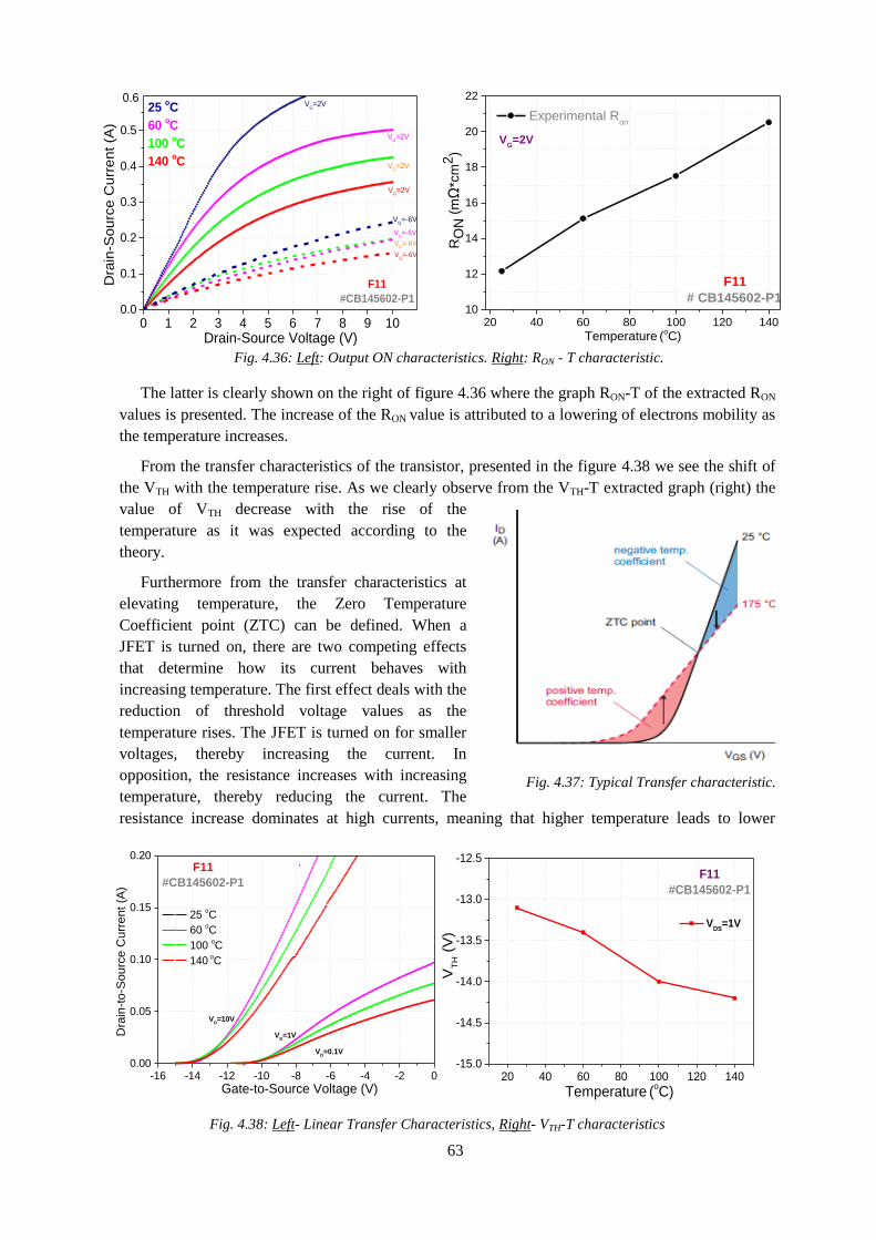
63
The latter is clearly shown on the right of figure 4.36 where the graph RON-T of the extracted RON
values is presented. The increase of the RON value is attributed to a lowering of electrons mobility as
the temperature increases.
From the transfer characteristics of the transistor, presented in the figure 4.38 we see the shift of
the VTH with the temperature rise. As we clearly observe from the VTH-T extracted graph (right) the
value of VTH decrease with the rise of the
temperature as it was expected according to the
theory.
Furthermore from the transfer characteristics at
elevating temperature, the Zero Temperature
Coefficient point (ZTC) can be defined. When a
JFET is turned on, there are two competing effects
that determine how its current behaves with
increasing temperature. The first effect deals with the
reduction of threshold voltage values as the
temperature rises. The JFET is turned on for smaller
voltages, thereby increasing the current. In
opposition, the resistance increases with increasing
temperature, thereby reducing the current. The
resistance increase dominates at high currents, meaning that higher temperature leads to lower
-16 -14 -12 -10 -8 -6 -4 -2 00.00
0.05
0.10
0.15
0.20
VD=0.1V
VD=1V
VD=10V
25 oC
60 oC
100 oC
140 oC
Dra
in-t
o-S
ou
rce
Cu
rre
nt
(A)
Gate-to-Source Voltage (V)
F11
#CB145602-P1
20 40 60 80 100 120 140-15.0
-14.5
-14.0
-13.5
-13.0
-12.5
VDS
=1V
Temperature (oC)
VT
H (
V)
F11
#CB145602-P1
Fig. 4.38: Left- Linear Transfer Characteristics, Right- VTH-T characteristics
Fig. 4.37: Typical Transfer characteristic.
0 1 2 3 4 5 6 7 8 9 100.0
0.1
0.2
0.3
0.4
0.5
0.6
VG=-6V
VG=-6V
VG=-6V
VG=-6V
VG=2V
VG=2V
VG=2V
VG=2V
Dra
in-S
ourc
e C
urr
ent
(A)
Drain-Source Voltage (V)
F11
#CB145602-P1
25 oC
60 oC
100 oC
140 oC
20 40 60 80 100 120 14010
12
14
16
18
20
22
Experimental Ron
VG=2V
F11
# CB145602-P1
Temperature (
oC)
RO
N (
mΩ
*cm
2)
Fig. 4.36: Left: Output ON characteristics. Right: RON - T characteristic.

64
currents. The threshold-voltage drop dominates at low currents, as we can clearly see in the transfer
characteristics. For a given VDS, there is a critical current below which the ID exhibits positive
temperature coefficient. Above this critical
current, the ID exhibits negative temperature
coefficient. This critical current corresponds to
the curve point, which is known as the Zero
Temperature Coefficient (ZTC) point. The
ZTC point is easily defined by the intersection
of the temperature curves.
For our measurements the reported values
follow: for VDS=0.1V ZTC≈-7.8V, for
VDS=1V ZTC≈-8.2V and for VDS=10V
ZTC≈-12V. The ZTC point is just an indicator
for the temperature behavior of the device and
is not usually mentioned in the device
datasheet.
In figure 4.39 the GS transistor forward graph is presented for temperature values up to 140°C.
We observe in the inset of the left graph the temperature dependence of the experimentally extracted
Vknee values accompanied by the theoretical temperature dependence of Vbi. It is obvious that the rise
of the temperature leads to smaller values of Vknee and Vbi. Particularly, the Vknee and Vbi shifts by 2.4
mV/°C and 1.3mV/°C respectively.
Blocking DC I-Vs in fluorinert
Testing in fluorinert must be performed for
evaluating the max blocking characteristics,
because it prevents the current leakage from the
surface of the device. The breakdown voltage
should be determined at low reverse current to
avoid self-heating. A rule of thumb is to not make
the measurements at a power density higher than
500W/cm2.
If the deviation between the on air (without
fluorinert) curve and the in fluorinert is great that
means that the surface leakage currents are
prominent.
Beside we can see this measurement performed
for one of the best F11 devices with a (slightly)
higher observed breakdown voltage values with
fluorinert than the respective without. The same trend was noted for all the measured best devices.
0 20 40 60 80 100 120 1400.0
0.5
1.0
1.5
2.0
2.5
3.0
3.5# CB 145602-P1
F11
-10V -20V -22V -30V-18V
VDS
(V)
I DS (
mA
)
Without Fluorinert
Fluorinert
Fig. 4.40: Blocking I-Vs with and without fluorinert.
0 1 2 3 4 50.0
0.2
0.4
0.6
0.8
1.0
1.2
1.4
20 40 60 80 100 120 1402.8
2.9
3.0
3.1
3.2
3.3
Vknee
(Extracted)
Vbi (Theoretical)
Temperature (oC)
Voltage (
V)
#CB145602-P1
S3P(3,9)F(1,1)
25oC 60
oC
100oC 140
oCG
ate
-to-S
ourc
e C
urr
ent (m
A)
Gate-to-Source Voltage (V)
140 oC
25oC
Fig. 4.39: G-S Forward I-Vs of transistor.

65
Choice of the best diodes
Determining the best diodes is not a priority. The main information to obtain from the best diodes
is the breakdown voltage, which is an upper limit for the corresponding transistors. The main
criterion for the choice will be the leakage current @200V. Then, the existence or not of double
barrier and the Vknee values follow in importance. The Vknee values for SiC diodes must be around
2.5V. Not much smaller, not much higher than this value. As in the case of the best transistors, a
deeper analysis must be eventually performed on these 5 best diodes.
We did not proceed to such an analysis for our sample because we were interested rather in the
transistors than the diodes, because such a device we are trying to develop for the incorporation in an
inverter. Besides this was the basic motivation for this work.
However, below the last set of measurements that must be performed on the best diodes are
presented. The graphs are from measurements on random devices and are indicative.
Reverse I-V measurements in fluorinert
Additional reverse measurements must be
performed in fluorinert in order to evaluate the
ultimate breakdown voltage values (if they are
higher, in absolute values than 200V) of the
device. The breakdown voltage should be
determined at low reverse current to avoid self-
heating of the diode. Therefore the voltage step
must be set to a rather high value (e.g. 0.5V) in
order to avoid the stress of the diode and the
consequent self-heating which leads to degraded
performance. The current compliance must be set
in a value that serves the power compliance of
500W/cm2.
High temperature characterization
High temperature measurements must be performed in order to evaluate diodes real operation
since in high current operation there is always a self-heating effect. From figure 4.42 where forward
0 1 2 3 4 5 60.0
0.2
0.4
0.6
0.8
1.0
1.2
1.4
1.6
1.8
2.0
140 oC 25
oC
#CB145602-P1
Diode
25 oC
60 oC
100 oC
140 oC
Cu
rrent (m
A)
Voltage (V)
-200 -160 -120 -80 -40 0-100
-80
-60
-40
-20
0
140oC25
oC
#CB145602-P1
Diode
Cu
rrent (u
A)
Voltage (V)
25 oC
60 oC
100 oC
140 oC
Fig. 4.42: Forward and Reverse DC Diode Characteristics
-400 -350 -300 -250 -200 -150 -100 -50 01E-10
1E-9
1E-8
1E-7
1E-6
1E-5
1E-4
Reverse Voltage (V)
Re
ve
rse C
urr
ent (A
)
# CB145602-P1
Diode
Fig. 4.41: Reverse measurement of diode.

66
and reverse characteristics of the diode are presented, we observe how the curves deviate with the
rise of the temperature. The reverse behavior of the diode deteriorates with the increase of the
temperature, while the rise of temperature leads to smaller Vknee values. During the reverse
measurement the room lights must be switched off in order to observe, as the reverse current
increases, if a light spot turn up on the diode.
4.6 Specifications tables
By the end of the electrical characterization of a processed sample, all the investigated, measured
and extracted parameters (specifications), must be gathered in one summarizing table, the
specifications (specs) table. The construction of the latter is very important as it summarizes the
great amount of the extracted information from the electrical characterization in a way that one can
refer to it and find easily any of the sample parameter without reading the whole sample’s
measurements report. The conditions under which the parameter is measured as well as its unit must
be explicitly mentioned. The reported value of the parameter can be the mean value of the five best
devices measured in the last stage of the characterization.
It must be mentioned at this point that the specs table constructed by the end of the on-wafer
electrical characterization of a sample is not the same as the specs table involved in a packaged
device datasheet. The reason is the different goals that they serve, since the first one provide
information mainly from the fabrication point of view and is addressed to process engineers while
the second one is directed rather at electronic engineers. Therefore after the packaging of a sample’s
device (usually the best one), additional measurements/extractions and calculations have to be
performed in order to fill the specs table of the packaged device datasheet.
Below we can see the specs tables for all the different under investigation devices from the
sample CB145602-P1. These tables summarize the whole work that has been done for the
characterization of it. The specs table of F11 transistor is extensive and involves several information
because this transistor exhibited by far better behavior than the other ones of the wider mesa widths.
It is something somehow expected in terms of the material, because the possibility of a defect in the
material increases with the increase of the mesa width. For the latter ones the specs tables provide
basic information since the interest for them is not very intense due to their not good behavior.

67
(T=25OC unless otherwise specified) F11 (Wnom=1.5um) Parameter Symbol Conditions Value Unit
Maximum Ratings
Max Pulsed Drain
Current IDPmax VGS=2V, VDS=VDsat 0.9 A
Breakdown G-S
Voltage BVGS IGS=15mA/cm2 (10.5μA) -13.5 V
Off Characteristics
Drain-Source
Blocking Voltage BVDS VGS=-28V, IDS= 2mA 125 V
Leakage Current Ileak
VDS=0V,VGS=-28V 38.5μ
A
VDS=0V,VGS=VTH 20.4μ
VDS=200V,VGS=-28V ∞
Gate Leakage
Current IGSS
VDS=0V, VGS=Vth-20V -11.6μ
VDS=200V, VGS=-10V ∞
Voltage Gain μ VDS=100V,
Iper=0.1mA/mm 4.1 -
ON Characteristics
Drain-Source On-
resistance RON VGS=0V
9.1 Ω
6.3 mΩ·cm2
Gate Threshold
Voltage VTH
VDS=0.1V 6.4 V VDS=1V 6.1
Gate Forward Current IG,FWD VGS=2V 3.39μ A
Knee Voltage Vknee - 2.3 V
Dynamic Characteristics
Input Capacitance Ciss
VGS=-16V
f=1MHz, osc.
level=100mV
VDS=0V 8.5
pF
VDS=40V 6.5
Output Capacitance Coss VDS=0V 7.7
VDS=40V -
Reverse Transfer
Capacitance Crss
VDS=0V 6.5
VDS=40V 3.9

68
(T=25OC unless otherwise specified) F31 (Wnom=2um)
Parameter Symbol Conditions Value Unit
Maximum Ratings
Max Pulsed Drain
Current IDPmax VGS=2V, VDS=VDsat 1.05 A
Breakdown G-S
Voltage BVGS IGS=15mA/cm2 (10.5μA) -15 V
Off Characteristics
Drain-Source
Blocking Voltage BVDS VGS=-34V, IDS= 2mA, 61 V
Leakage Current Ileak
VDS=200V,VGS=-34V ∞ A
ON Characteristics
Drain-Source On-
resistance RON VGS=0V
16 Ω
11.1 mΩ·cm2
Gate Threshold
Voltage VTH VDS=0.1V -13.3 V
Knee Voltage Vknee - 2.3 V
(T=25OC unless otherwise specified) F12 (Wnom=2.5um)
Parameter Symbol Conditions Value Unit
Maximum Ratings
Max Pulsed Drain
Current IDPmax VGS=2V, VDS=VDsat 1.2 A
Breakdown G-S
Voltage BVGS IGS=15mA/cm2 (10.5μA) -17.9 V
Off Characteristics
Drain-Source
Blocking Voltage BVDS VGS=-40V, IDS= 2mA, 47 V
Leakage Current Ileak
VDS=200V,VGS=-40V ∞ A
ON Characteristics
Drain-Source On-
resistance RON VGS=0V
13.2 Ω
9.2 mΩ·cm2
Gate Threshold
Voltage VTH VDS=0.1V -22.1 V
Knee Voltage Vknee - 2.5 V

69
(T=25OC unless otherwise specified) F32 (Wnom=3um)
Parameter Symbol Conditions Value Unit
Maximum Ratings
Max Pulsed Drain
Current IDPmax VGS=2V, VDS=VDsat 1.4 A
Breakdown G-S
Voltage BVGS IGS=15mA/cm2 (10.5μA) -11.2 V
Off Characteristics
Drain-Source
Blocking Voltage BVDS VGS=-40V, IDS= 2mA, 13 V
Leakage Current Ileak
VDS=200V,VGS=-40V ∞ A
ON Characteristics
Drain-Source On-
resistance RON VGS=0V
16.1 Ω
11.2 mΩ·cm2
Gate Threshold
Voltage VTH VDS=0.1V -29.3 V
Knee Voltage Vknee - 2 V
(T=25OC unless otherwise specified) F42 (Wnom=3um, #n=121)
Parameter Symbol Conditions Value Unit
Maximum Ratings
Max Pulsed Drain
Current IDPmax VGS=2V, VDS=VDsat 2.1 A
Breakdown G-S
Voltage BVGS IGS=15mA/cm2 (10.5μA) -7 V
ON Characteristics
Drain-Source On-
resistance RON VGS=0V
196 Ω
136 mΩ·cm2
Gate Threshold
Voltage VTH VDS=0.1V - V
Knee Voltage Vknee - 1.9 V

70
(T=25OC unless otherwise specified) F23 (Wnom=4um)
Parameter Symbol Conditions Value Unit
Maximum Ratings
Max Pulsed Drain
Current IDPmax VGS=2V, VDS=VDsat 1.43 A
Breakdown G-S
Voltage BVGS IGS=15mA/cm2 (10.5μA) -16.9 V
ON Characteristics
Drain-Source On-
resistance RON VGS=0V
8.9 Ω
6.2 mΩ·cm2
Gate Threshold
Voltage VTH VDS=0.1V <-40 V
Knee Voltage Vknee - 2.5 V
(T=25OC unless otherwise specified) F33 (Wnom=5um)
Parameter Symbol Conditions Value Unit
Maximum Ratings
Max Pulsed Drain
Current IDPmax VGS=2V, VDS=VDsat 1.6 A
Breakdown G-S
Voltage BVGS IGS=15mA/cm2 (10.5μA) -14 V
ON Characteristics
Drain-Source On-
resistance RON VGS=0V
30.7 Ω
21.3 mΩ·cm2
Gate Threshold
Voltage VTH VDS=0.1V <-40 V
Knee Voltage Vknee - 2.4 V
By studying carefully the tables, we can summarize the performance of the sample devices in the
following basic conclusions.
Low quality of Gate-Source junction for all the transistors, especially for the reverse regime
where low BVGS values were reported. Consequent high values of G-S leakage current.
Increase of the max pulsed Drain current (IDPmax) with the increase of the mesa width or the area
of the device (F42) but relatively low values.
Very low blocking capability with the BVDS values being except for the F11, lower than 100V.
Ron values in the moderate range.
From the above, we deduce that the devices of the processed sample are away from the desired
specifications for our application, therefore a new fabrication effort must be done with improved and
more precise fabrication procedure and maybe new optimized structure.

71
4.7 Conclusions
In this chapter the typical measurements procedure that must be followed for the elaborate on
wafer electrical characterization of a sample was minutely presented. Simultaneously the results of
the electrical characterization of the sample CB145602-P1 were presented. From them, we observed
that there are many fields (e.g. the blocking capability) where the performance of the JFETs must be
optimized. For that reason a second effort has been done with the run of a new sample, the
CB145602-P4 where some modifications have been done rather to the design of the device than the
followed fabrication process. The characterization of the sample will reveal if we managed to vanish
the observed malfunctions and get acceptable overall behavior from the JFETs. In the next chapter,
this new sample is investigated elaborately.

72
Chapter 5. Measurement results from sample CB145602-P4
Due to the low performance that the first sample exhibited in some fields, a second one was
decided to be fabricated in a new run, featuring some differentiations. The main modification that
was adopted is the deeper implantation of the gate regions which now equals to 1.1um. Let us
remind that for the first sample the implantation depth was equal to 0.3um.
In this chapter the measurements results from the electrical characterization of the second under
investigation sample, the CB145602-P4 are presented. The proper measurements procedure,
described in the previous chapter has been followed.
5.1 Transistor geometry determination.
The mask layout is the same as for the first sample CB145602-P1. Below we can see the
dimensions, the shape and a photo of the processed sample which consists of 20 periods.
Fig. 5.1: Top left: Period of the mask. Top right: Schematic and photo of the processed sample.
Bottom: TLM patterns for both n-type (on the left) and p-type contacts (on the right).
300μm
Implantation Depth=1.1μm 300μm

73
Above we see the placement of the processed piece on the initial 4H-SiC wafer. By observing
again the figure 3.1 we see that no defects were detected in that region. In this way, possible
malfunctions and bad behavior of the devices must be attributed rather to the processing procedure
than the material. Important dimensions are also obvious on the cross section on the right.
Below SEM images from different fabrication steps are presented.
The main modification adopted in this sample, as has been already mentioned, is the different
implantation depth. Moreover the etching for the formation of the trenches has stopped at 2um depth
(the respective depth for the first sample was equal to 2.5um). In this way, as we can see from the
cross section graph, the channel consists of 2 different doping concentrations. In depth of 0.2μm the
doping is 1E+16 cm-3
, whilst for the rest 0.9μm is the same as the doping of the drift region namely
1E+15cm-3
.
Important values in dimensions and doping of different parts of the device are shown below.
Fig. 5.3: SEM images Left- after the RIE etching for source finger formation. Middle-Right- after 3 hours oxidation.
Fig. 5.2: Right: Position of CB145602-P4 on the 4-inch 4H-SiC wafer slice Left: Important dimension parameters shown.
Ldr=7.1 (8-0.9) μm,
Lchannel= 1.9μm (gate length (1.1)+Vbi depletion width (0.8)),
Lp=2μm (1+1)

74
ρsub
(Ω•cm)
Lsub
(μm)
Lbuf
(μm)
ND (cm-3
)
buffer
Ldrift
(μm)
ND (cm-3
)
drift
Lchan
(μm)
0.021 372 1 1.00E+18 7.1 5.00E+15 1.9
Lpill/ch
(μm)
ND (cm-3
)
pillar/chan
Lpill/con
(μm)
ND (cm-3
)
pillar/cont
Gate length
LG (μm)
NA (cm-3
)
gate
ND(cm-3
)
channel
1 1.00E+16 1 1.00E+19 1.1 1.00E+19 1E+16 (0.2μm)
5E+15 (0.9μm)
Channel
width
W=2a(μm)
Nfing
Gate
pitch
WG (μm)
Rcont.
(Ω•cm2)
Pillar width
Wpil (μm) Lpillar
Ζ
(μm)
WGR
(μm)
2/2.5/3/3.
5/4.5/5.5
50/47/43/4
0/34/31 3.5 0.0001 W-0.45 2μm 256 3.5
Wbus
(μm)
W1
(μm)
W2
(μm)
W3
(μm)
W4
(μm)
W5
(μm) W6 μm)
13.75 3 3 3.5 4 4.5 6
* * Lchan=1.9μm (gate length/implantation depth (1.1 μm)+Vbi depletion width (0.8μm))
In the table above W, WG, W1,W2, …, W6, WGR are the actual dimensions calculated after the
observation on the SEM photos. From the observation on them we concluded that the W and the W1,
W2, …, W6 in comparison with the mask dimensions, are increased approximately by 0.5μm and
consequently the WG and WGR are approximately minus 0.5μm. Like the case of the first sample the
available SEM photos were few, so we have to keep a prejudice on the actual dimensions.
Since the mask layout is the same, the active area, active perimeter as well as the Total finger
area take the same values as for the first sample.
5.2 Theoretical values estimation of parameters
In the following table we can see the theoretically expected parameters values of all the different
transistors of CB145602-P4 sample at RT (300K). Refer to Appendix 2 for the utilized equations.
Table of Parameters Theoretical Values
F W
(μm)
WG
(μm)
Source
Area
(10-4 cm2)
Active Area
(10-4 cm2)
VG=0V VG=2V VTH
(V)
Rsh
(Ω/sq)
[con. layer]
Rsh
(Ω/sq)
[G layer]
BVGS
@RT
(V) (Ω) (mΩ*cm2) (Ω) (mΩ*cm2)
11 2
3.5
1.92 6.94 11.1 7.68 6.39 4.44 -2.53
79.6 72.4 322
21 2.5 2.41 7.12 6.95 4.95 5.3 3.77 -5.65
31 2.5 2.41 6.94 6.95 4.82 5.3 3.67 -5.65
41 3 2.75 7.05 5.9 4.16 4.91 3.46 -9.46
12 3 2.75 7.05 5.9 4.16 4.91 3.46 -9.46
22 3.5 3.07 7.07 5.3 3.75 4.62 3.26 -13.96
32 3.5 3.07 7.07 5.3 3.75 4.62 3.26 -13.96
13 4.5 3.48 6.86 4.81 3.3 4.39 3.01 -25.03
23 4.5 3.48 6.86 4.81 3.3 4.39 3.01 -25.03
33 5.5 3.97 7.04 4.35 3.06 4.06 2.86 -38.87
42 3.5 9.29 21.48 1.75 3.76 1.53 3.28 -13.96

75
Table of Resistance Theoretical Values (R)
mesαW
(μm) #n
Rcont.D
(Ω)
Rsub
(Ω)
Rbuf
(Ω)
Rdrift
(Ω)
Rch1
.
(Ω)
Rch2.
(Ω)
Rpil.1
(Ω)
Rpil.2
(Ω)
Rcont.S
(Ω)
RΟΝ
(Οhm)
2 50 0.142 1.11 0.003 3.70 4.860 0.53 0.300 0.003 0.390 11.1
2.5 47 0.139 1.08 0.003 2.85 2.298 0.36 0.255 0.003 0.332 6.95
3 43 0.140 1.09 0.003 2.51 1.612 0.29 0.233 0.002 0.302 5.9
3.5 40 0.140 1.09 0.004 2.29 1.275 0.24 0.215 0.002 0.280 5.3
4.5 34 0.111 0.86 0.003 1.62 0.759 0.16 0.152 0.002 0.198 4.81
5.5 31 0.106 0.82 0.003 1.44 0.607 0.13 0.134 0.001 0.173 4.35
3.5 121 0.046 0.36 0.001 0.76 0.421 0.08 0.071 0.001 0.093 1.75
For the contact resistances Rcon,D and Rcont,S the common value of 10-4
Ohm·cm2 has been used.
In the last table, a detailed analysis of the Ron is
presented. We can see all the individual resistance
values which constitute the Ron, expressed in Ohms.
The values are calculated for VGS=0V. In the graph
beside we see the theoretical dependence of VTH on
channel width.
5.3 First run of measurements in one mask period
The period P15 was selected for the first run of measurements as the involved devices seem to
have good morphology.
Measurements of TLM patterns
The TLM patterns on n-type material were not operational due to a mask-design problem. The
measurements on the p type TLMs revealed a bad behavior of the patterns, thus the analysis did not
proceed further.
Measurements of single diodes
The extracted parameters from the measurements on the unique diode of the period are shown
below. The differential resistance Rdiff is determined at V=4V and 5V since the forward current
density values of 10A/cm2 (6.9mA) and 40A/cm
2 (27.8mA) are not reached.
Vknee= Vmin=2.1V,
Νo Double Barrier,
Ileak=-4.36 x10⁻⁸
A (@200V),
Rdiff= 283286 Ω (@4V), Rdiff=757576 Ω (@5V).
1.0 1.5 2.0 2.5 3.0 3.5 4.0 4.5 5.0 5.5-30
-25
-20
-15
-10
-5
0
Channel Width (μm)
VT
H (
V)
#CB145602
Fig. 5.4: VTH dependence on channel width.
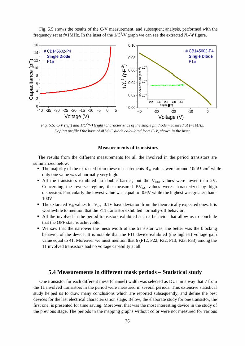
76
Fig. 5.5 shows the results of the C-V measurement, and subsequent analysis, performed with the
frequency set at f=1MHz. In the inset of the 1/C2-V graph we can see the extracted Nd-W figure.
Measurements of transistors
The results from the different measurements for all the involved in the period transistors are
summarized below:
The majority of the extracted from these measurements Ron values were around 10mΩ·cm2 while
only one value was abnormally very high.
All the transistors exhibited no double barrier, but the Vknee values were lower than 2V.
Concerning the reverse regime, the measured BVGS values were characterized by high
dispersion. Particularly the lowest value was equal to -0.6V while the highest was greater than -
100V.
The extarcted Vth values for VDS=0.1V have deviation from the theoretically expected ones. It is
worthwhile to mention that the F11 transistor exhibited normally-off behavior.
All the involved in the period transistors exhibited such a behavior that allow us to conclude
that the OFF state is achievable.
We saw that the narrower the mesa width of the transistor was, the better was the blocking
behavior of the device. It is notable that the F11 device exhibited (the highest) voltage gain
value equal to 41. Moreover we must mention that 6 (F12, F22, F32, F13, F23, F33) among the
11 involved transistors had no voltage capability at all.
5.4 Measurements in different mask periods – Statistical study
One transistor for each different mesa (channel) width was selected as DUT in a way that 7 from
the 11 involved transistors in the period were measured in several periods. This extensive statistical
study helped us to draw many conclusions which are reported subsequently, and define the best
devices for the last electrical characterization stage. Below, the elaborate study for one transistor, the
first one, is presented for time saving. Moreover, that was the most interesting device in the study of
the previous stage. The periods in the mapping graphs without color were not measured for various
-40 -35 -30 -25 -20 -15 -10 -5 0 50
2
4
6
8
10
12
14
16
# CB145602-P4
Single Diode
P15
Ca
pa
cita
nce
(p
F)
Voltage (V)
-40 -30 -20 -10 00.00
0.02
0.04
0.06
0.08
0.10
2.2 2.4 2.6 2.8 3.0
1015
1016
1017
Co
nc
en
tra
tio
n (
cm
-3)
Depth (m)
# CB145602-P4
Single Diode
P15
Voltage (V)
1/C
2 (
pF
-2)
Fig. 5.5: C-V (left) and 1/C2(V) (right) characteristics of the single pn diode measured at f=1MHz.
Doping profile f the base of 4H-SiC diode calculated from C-V, shown in the inset.

77
reasons (sample edge, problematic measurements etc). Since the sample is a small one, all the
periods of our sample were examined, thus the statistical sample was equal to 20 devices.
Statistical study has been also performed for the TLMs and the diodes of the sample but are not
presented as they are out of the scope of our application.
Transistors
Gate-Source characteristics:
0
2
4
6
8
10
12
14
16
18
F11
GS Diodes
#C
ells
d_b
no d_b
d_b
no d_b
GS diodes
(3,5)(1,5)
(2,6) (3,6)(1,6)
(2,5)
(1,4) (2,4)
(3,3)
(3,4)
(2,3)(1,3)
(2,2)(1,2)
(1,1)
(2,7)(1,7)
(3,1)(2,1)
1.9
2.1
(3,2)
Fig. 5.6: Histogram (left) and mapping (right) of the existence or not of a double barrier in the GS diode.
1.0 1.2 1.4 1.6 1.8 2.0 2.2 2.4 2.6 2.8 3.00
1
2
3
4
5
6
7
F11
G-S diode VKNEE
Volts
# C
ell
s
VKNEE
: (Volts)
(3,5)(1,5)
(2,6) (3,6)(1,6)
(2,5)
(1,4) (2,4)
(3,3)
(3,4)
(2,3)(1,3)
(2,2)(1,2)
(1,1)
(2,7)(1,7)
(3,1)(2,1)
1.0
1.2
1.4
1.6
1.8
2.0
2.2
2.4
2.6
(3,2)
Fig. 5.7: Histogram (left) and mapping (right) of the gate-source-diode knee voltage.

78
We observe that as the mesa width increases, more devices are detected with double barrier.
It’s remarkable that for the F11 (narrowest) transistor only one device was detected with
double barrier while for the last two JFETs F23 and F33 (widest), half the measured devices
exhibited double barrier.
Although, for a SiC diode the expected Vknee value is higher than 2V, many values lower
than this value were reported.
As for the BVGS values namely the quality of the GS junction in the reverse regime,
undoubtedly is much improved in comparison with the first sample CB145602-P1 since for
all the devices many high (absolute) values were measured while for this first sample P1 the
majority of the BVGS values are placed in the first ten of the reverse voltage axis. It is
noteworthy that more than half the F11 devices did not reach the current limit value
(10.5μA) up to -65V bias, the limit of the measurement range. Thus we can deduce the
satisfactory overall performance of the GS junction, which is usually a very challenging and
critical fabrication step. The latter is reinforced by the results about the existence of double
barrier.
By checking in the same time the BVGS and the double barrier characteristics, we observed that
the devices with high BVGS values were also detected without double barrier.
Drain-source ON characteristics:
0 5 10 15 20 250
1
2
3
4
5
6
F11
mΩ*cm2
RON
(VGS
= 0V)
#C
ell
s
RON
> 25mΩ*cm2
RON
: (mΩ*cm2)
(3,5)(1,5)
(2,6) (3,6)(1,6)
(2,5)
(1,4) (2,4)
(3,3)
(3,4)
(2,3)(1,3)
(2,2)(1,2)
(1,1)
(2,7)(1,7)
(3,1)(2,1)
5.0
7.5
10.0
12.5
15.0
17.5
20.0
22.5
25.0
(3,2)
Fig. 5.9: Histogram (left) and mapping (right) of the transistors RON.
-65 -60 -55 -50 -45 -40 -35 -30 -25 -20 -15 -10 -5 00
2
4
6
8
10
12
14
F11
BVGS
<-65V
#C
ells
Volts
BVGS
at IGS
= -15mA/cm2
BVGS
(V)
(3,5)(1,5)
(2,6) (3,6)(1,6)
(2,5)
(1,4) (2,4)
(3,3)
(3,4)
(2,3)(1,3)
(2,2)(1,2)
(1,1)
(2,7)(1,7)
(3,1)(2,1)
-65
-55
-45
-35
-25
-15
-5
0
(3,2)
Fig. 5.8: Histogram (left) and mapping (right) of the gate-source-diode BVGS

79
We observe that the majority of the Ron values for the transistor F11 are higher than 10mΩ·cm2,
but generally the reported for all the under test devices values were mainly around 10mΩ·cm2.
The great improvement in comparison with the sample CB145602-P1, is that no extreme values
at all have been reported and even the higher ones were lesser than 50mΩ·cm2, entirely unlike the
first sample. So we can deduce that the largest part of the transistors exhibit good behavior and
they have satisfactory low Ron values. Moreover, from the mapping graphs, although the sample
dimensions are small we see some spatial dependence with the lower Ron values measured from
transistors placed on the bottom side of the sample. No dependence of the Ron on the existence of
double barrier or the BVGS was noticed.
Transfer characteristics:
We observe that the values are placed in a range of 2V. The same trend was observed for all the
devices with the majority of the values around a specific value. This concentrated distribution can
be considered as the proof for the “real” value of VTH.
Some spatial dependence was noted as for the first sample. By observing again the fig. 5.2 and
the placement of the sample on the initial wafer, this dependence can be probably explained since
we know from the supplier of the wafer that the regions on the edges, in a distance up to even
1cm, are not perfectly fabricated.
5.5 Measurements of best devices
Choice of the best transistors
Based on the elaborate statistical study of the
previous stage, the best devices for every different
transistor according to the dimensions were defined.
The characterization goes on with measurements
performed selectively only on best transistors. In the
graph beside we see characteristically the placement
on the sample of the best F11 devices.
The orange cells indicate the periods where
transistors were measured while the periods where
-1.2 -1.0 -0.8 -0.6 -0.4 -0.2 0.0 0.2 0.4 0.6 0.8 1.0 1.20
1
2
3
4
5
6
F11VTH
VDS
= 0.1V
Volts
#C
ells
VDS
=0.1V
VTH
(V)
(3,5)(1,5)
(2,6) (3,6)(1,6)
(2,5)
(1,4) (2,4)
(3,3)
(3,4)
(2,3)(1,3)
(2,2)(1,2)
(1,1)
(2,7)(1,7)
(3,1)(2,1)
-1.2
-1.0
-0.8
-0.6
-0.4
-0.2
0.0
0.2
0.4
0.6
0.8
(3,2)
Fig. 5.10: Histogram (left) and mapping (right) of the transistors VTH.
F11
(3,5)(1,5)
(2,6) (3,6)(1,6)
(2,5)
(1,4) (2,4)
(3,3)
(3,4)
(2,3)(1,3)
(2,2)(1,2)
(1,1)
(2,7)(1,7)
(3,1)(2,1)
1.0
2.0
3.0
(3,2)
Under
Test
Best
Fig. 5.11: Placement of the best F11 devices.

80
the measurements were not feasible are left blank. The green cells indicate the periods where the
best devices were detected.
Pulsed measurements
Pulsed measurements were performed to some of the best F11 (Wnom=1.5um), F32 (Wnom=3um)
and F23 (Wnom=4um) devices. In the measurements presented below, pulsed sweep was imposed on
the Drain and DC step bias on the Gate. The measurement conditions follows: pulse width: 200μsec,
time-off: 1sec, measurement time: 119μsec. Keithley SMUs 2602 and 2651 were utilized.
We clearly observe that as wider the channel is, higher current values are reached, while is more
difficult to turn the JFET off. We see that the narrowest device, the transistor F11 is turned off by a
reverse bias on the gate lesser than -1V despite the wider transistor F23 which is not turned off up to
-36V.
C-V measurements
Capacitance measurements were performed selectively to some transistors. Normal behavior was
observed for all. The Ciss, Coss and Crss curves are
shown characteristically for one of the best F11
devices. The measurement conditions are shown in
the inset (f=1MHz, VGS=-10V). Complementary,
since C-V measurements were not performed during
the study in one mask period, also the CGD-VGD, CGS-
VGS and CDS-VDS measurements are presented below
in the figure 5.14. All the measured capacitance
values are in the order of picos (pF). It is obvious
that the formulas Ciss= CGD+CGS, Coss= CGD+CDS and
Crss= CGD are demonstrated by the graphs.
Remarkable are the very small, almost negligible
value of CDS, the constant, unaffected by VDS, value
0 1 2 3 4 5 6 7 8 9 10 11 12 130.00
0.05
0.10
0.15
0.20
0.25
21F11
11F11
Pulsed meas. VGS
=2...-3, step=1
Drain Voltage (V)
D
rain
Cu
rren
t (A
)
0 1 2 3 4 5 6 7 8 9 10 11 12 13 14 15
0.0
0.2
0.4
0.6
0.8
1.0
1.2
22F32
34F32
VGS
=-16V
VGS
=-10V
VGS
=-4V
VGS
=0V
VGS
=2VPulsed meas.
Drain Voltage (V)
Dra
in C
urr
en
t (A
)
0 1 2 3 4 5 6 7 8 9 10 11 12 13 14 15 16 170.0
0.3
0.6
0.9
1.2
1.5
12F23
22F23
VGS
=-24V
VGS
=-12V
VGS
=-36V
VGS
=0VPulsed meas.
Dra
in C
urr
en
t (A
)
Drain Voltage (V)
Fig. 5.12: Pulsed ON characteristics. There is obviously a large difference between the devices in terms of current value.
0 5 10 15 20 25 30 35 400
2
4
6
8
10
P11F11
f=1MHz
VGS
=-10V
Coss
Crss
Ciss
C
ap
acit
an
ce (
pF
)
Drain-Source Voltage (V) Fig. 5.13: CISS, COSS and CRSS at f=1MHz.

81
of CGS as well as the discontinuity of the CGD curve near zero voltage namely the threshold voltage
of the device. Accordingly, the CGS curve at this (threshold) voltage value exhibits an abrupt
inflexion. The CGD, unlike the CGS exhibits a continuously descending tense due to the expansion of
the depletion region within the drift region of the transistor.
Moreover, from the fig. 5.13 we distinguish a very small deviation between the Coss and Crss
which differ in their definitions by the CDS. This deviation is explained by the CDS-VDS graph and the
very low value of the capacitance.
For extensive details about the C-V measurements is recommended to refer to Appendix 1.
Blocking DC I-Vs in fluorinert
Testing in fluorinert is performed for evaluating the maximum blocking voltage which is
determined at low reverse current to avoid self-heating. For these measurements a curve tracer
Tektronix 370A was utilized. Below we see the measurements for one of the best for all the different
under test devices.
It is obvious that the best blocking behavior as it was expected belongs to the narrowest transistor
F11 (channel width=1.5um) as its blocking capability for gate voltage equal to -18V approached the
value of 800V while the F23 with channel width equal to 4um can block less than 14V when biased
at the Gate with -40V. It is obvious that the blocking capability is inversely proportional to the
channel width.
-40 -35 -30 -25 -20 -15 -10 -5 00
2
4
6
8
10
12
14
16
18
VTH
=0.34V
P11F11
Voltage (V)
CGS
CGD
f=1MHz
Cap
acit
an
ce (
pF
)
0 5 10 15 20 25 30 35 400
1
2
3
4
5
6
7
8
P11F11
CGS
CGD
f=1MHz
VGS
=-10V
Ca
pa
cit
an
ce
(p
F)
Drain-Source Voltage (V)
0 5 10 15 20 25 30 35 400.10
0.15
0.20
0.25
0.30
P11F11
CDS
f=1MHz
VGS
=-10V
Drain-Source Voltage (V)
Cap
acit
an
ce (
pF
)
Fig. 5.14: At f=1MHz, CGD-VGD and CGS-VGS, CGD-VDS and CGS-VDS,
CDS-VDS measurements.

82
Choice of the best diodes
Although the diodes are out of the scope of
our work, due to the improved performance of the
transistors and the special interest that has come up,
measurements have been also performed to the best
diodes. These have been defined with the proposed
in the previous chapter procedure are presented in
the figure 5.16. The best diodes were detected in
the green marked periods.
0 100 200 300 400 500 600 700 800 9000.0
0.2
0.4
0.6
0.8
1.0
F11
-18V-14V
-10V
-6V
VGS
=-2V
Dra
in C
urre
nt
(m
A)
Drain Voltage (V)
0 50 100 150 200 250 300 350 400 450 5000.0
0.1
0.2
0.3
0.4
0.5 F31-10V
-14V
-18V
-22V
-26V
Drain Voltage (V)
Drain
Cu
rrent (m
A)
0 50 100 150 200 250 300 350 400 4500.0
0.5
1.0
1.5
2.0
2.5
3.0
3.5
F12
-40V
-36V
-32V
-28V
-24V
VGS
=-20V
Drain Voltage (V)
Dra
in C
urre
nt
(m
A)
0 20 40 60 80 100 120 140 160 1800.0
0.4
0.8
1.2
1.6
2.0
2.4
F32
-40V
Drain Voltage (V)
Dra
in C
urre
nt
(m
A)
-36V
-32V
-28V
-24V
VGS
=-20V
0 20 40 60 80 100 120 140 160 1800
1
2
3
4 F42
-40V
-20V-24V
-28V
-32V
-36V
Drain Voltage (V)
Dra
in C
urre
nt
(m
A)
0 2 4 6 8 10 12 140
1
2
3
4
5
F23V
GS=-32V -36V -40V
Drain Voltage (V)
Dra
in C
urre
nt (m
A)
Fig. 5.15: Blocking I-V characteristics of best devices in fluorinert.
Diodes
(3,5)(1,5)
(2,6) (3,6)(1,6)
(2,5)
(1,4) (2,4)
(3,3)
(3,4)
(2,3)(1,3)
(2,2)(1,2)
(1,1)
(2,7)(1,7)
(3,1)(2,1)
1.0
2.0
3.0
(3,2)
Under
Test
Best
Fig. 5.16: Placement of the best Diodes.

83
Reverse I-V measurements in fluorinert
The electrometer Keithley 6517 is used while
the compliance is set in a value that serves the
power compliance of 500W/cm2
. Since the area of
the square diode is 9E-4cm2 (300um·300um), the
current compliance is set to 0.9mA. In the figure
we can see the reverse I-V of the best diode.
Generally, the 5 best diodes exhibited blocking
capability higher than -600V. The highest
evaluated value is equal to -677V.
5.6 Specifications tables
The specs tables for the diode and the under test transistors are presented below and are of great
importance as they summarize the great amount of the extracted information. Specs tables are filled
for all the devices except of transistor F33 (the wider one) which exhibited bad behavior and there is
rather no further interest about it.
The table of F11 transistor is extensive as this device exhibited better behavior than the other
ones of the wider mesa widths. For the latter ones the specs tables provide basic information since
the interest for them is not very intense.
For more information and instructive details about the construction of specs table refer to the
respective section of the previous chapter.
Diode Parameter Symbol Conditions Value Unit
Breakdown Voltage VBR - 660 V
Leakage Current Ileak V=-200V -3.6n A
Knee Voltage Vknee - 2.1 V
-700 -600 -500 -400 -300 -200 -100 0-0.4
-0.3
-0.2
-0.1
0.0
# CB145602-P4
P22 Diode
Reverse Voltage (V)
Re
ve
rse C
urr
ent (m
A)
Fig. 5.17: Reverse measurement.

84
(T=25OC unless otherwise specified) F11 (Wnom=1.5um)
Parameter Symbol Conditions Value Unit
Maximum Ratings
Max Pulsed Drain
Current IDPmax VGS=2V, VDS=VDsat 0.22 A
Breakdown G-S
Voltage BVGS IGS=15mA/cm2 (10.5μA) <-65 V
Off Characteristics
Drain-Source
Blocking Voltage BVDS VGS=-18V, IDS= 0.5mA, 800 V
Leakage Current Ileak
VDS=0V,VGS=-10V < E-8
A VDS=200V,VGS=-10V < E-8
Gate Leakage
Current IGSS
VDS=0V, VGS=-20V < E-8
VDS=200V, VGS=-10V < E-8
Voltage Gain μ VDS=100V,
Iper=0.1mA/mm 51 -
ON Characteristics
Drain-Source On-
resistance RON VGS=0V
17.7 Ω
12.3 mΩ·cm2
Gate Threshold
Voltage VTH
VDS=0.1V 0.25 V
VDS=1V 0.17
Gate Forward Current IG,FWD VGS=2V 2E-7 A
Knee Voltage Vknee - 1.8 V
Dynamic Characteristics
Input Capacitance Ciss
VGS=-10V
f=1MHz, osc.
level=100mV
VDS=0V 9.9
pF
VDS=40V 6.6
Output Capacitance Coss VDS=0V 7.4
VDS=40V 4.1
Reverse Transfer
Capacitance Crss
VDS=0V 7.3
VDS=40V 3.9

85
(T=25OC unless otherwise specified) F31 (Wnom=2um)
Parameter Symbol Conditions Value Unit
Maximum Ratings
Breakdown G-S
Voltage BVGS IGS=15mA/cm2 (10.5μA) -48 V
Off Characteristics
Drain-Source
Blocking Voltage BVDS VGS=-26V, IDS= 0.4mA, 470 V
Leakage Current Ileak
VDS=0V,VGS=-24V <E-8
A VDS=200V,VGS=-24V 2.7E-6
Gate Leakage
Current IGSS
VDS=0V, VGS=-24V 1.4E-7
VDS=200V, VGS=-24V 1.1E-8
Voltage Gain μ VDS=100V,
Iper=0.1mA/mm 17.2 -
ON Characteristics
Drain-Source On-
resistance RON VGS=0V
10.1 Ω
7 mΩ·cm2
Gate Threshold
Voltage VTH
VDS=0.1V -3.4 V
VDS=1V -3.7
Gate Forward Current IG,FWD VGS=2V 7.6E-8 A
Knee Voltage Vknee - 1.9 V
(T=25OC unless otherwise specified) F12 (Wnom=2.5um)
Parameter Symbol Conditions Value Unit
Maximum Ratings
Breakdown G-S
Voltage BVGS IGS=15mA/cm2 (10.5μA) <-40 V
Off Characteristics
Drain-Source
Blocking Voltage BVDS VGS=-28V, IDS= 1mA, 176 V
Voltage Gain μ VDS=100V,
Iper=0.1mA/mm 3.5 -
ON Characteristics
Drain-Source On-
resistance RON VGS=0V
9.1 Ω
6.3 mΩ·cm2
Gate Threshold
Voltage VTH VDS=0.1V -7.4 V
Gate Forward Current IG,FWD VGS=2V 1.6μ A
Knee Voltage Vknee - 2.4 V

86
(T=25OC unless otherwise specified) F32 (Wnom=3um)
Parameter Symbol Conditions Value Unit
Maximum Ratings
Max Pulsed Drain
Current IDPmax VGS=2V, VDS=VDsat 1.21 A
Breakdown G-S
Voltage BVGS IGS=15mA/cm2 (10.5μA) <-40 V
Off Characteristics
Drain-Source
Blocking Voltage BVDS VGS=-34V, IDS= 1mA, 85.2 V
Voltage Gain μ VDS=100V,
Iper=0.1mA/mm 2.6 -
ON Characteristics
Drain-Source On-
resistance RON VGS=0V
12.1 Ω
8.4 mΩ·cm2
Gate Threshold
Voltage VTH VDS=0.1V -13.4 V
Gate Forward Current IG,FWD VGS=2V 1.3μ A
Knee Voltage Vknee - 2.4 V
(T=25OC unless otherwise specified) F42 (Wnom=3um)
Parameter Symbol Conditions Value Unit
Maximum Ratings
Breakdown G-S
Voltage BVGS IGS=15mA/cm2 (10.5μA) -36.3 V
Off Characteristics
Drain-Source
Blocking Voltage BVDS VGS=-34V, IDS= 1mA, 75 V
Voltage Gain μ VDS=100V,
Iper=0.1mA/mm 2.5 -
ON Characteristics
Drain-Source On-
resistance RON VGS=0V
40.4 Ω
28.1 mΩ·cm2
Gate Threshold
Voltage VTH VDS=0.1V -13.6 V
Gate Forward Current IG,FWD VGS=2V 1.2μ A
Knee Voltage Vknee - 2.2 V

87
(T=25OC unless otherwise specified) F23 (Wnom=4um)
Parameter Symbol Conditions Value Unit
Maximum Ratings
Max Pulsed Drain
Current IDPmax VGS=2V, VDS=VDsat 1.4 A
Breakdown G-S
Voltage BVGS IGS=15mA/cm2 (10.5μA) <-40 V
Off Characteristics
Drain-Source
Blocking Voltage BVDS VGS=-40V, IDS= 2mA, 12.7 V
ON Characteristics
Drain-Source On-
resistance RON VGS=0V
8.9 Ω
6.2 mΩ·cm2
Gate Threshold
Voltage VTH VDS=0.1V -29.6 V
Gate Forward Current IG,FWD VGS=2V 1.4μ A
Knee Voltage Vknee - 2.3 V
By studying carefully the tables, we can summarize the performance of the sample devices in
the following basic conclusions.
High blocking value for the diode.
In accordance with the diode very good blocking capability especially for the narrow
devices. This is an outstanding improvement in comparison with the first sample,
CB145602-P1 where low blocking values were measurements even for the transistor with
the narrowest channel.
For the F11 device (narrowest one) satisfactory values for BVDS and voltage gain. The
exhibited normally-off behavior is also accounted as an extra advantage.
Good reported voltage gain values as a consequence of the blocking capability.
Exceptional performance of the Gate-Source diode as for the reverse regime where very
high (absolute) BVGS values were reported. Consequently the G-S leakage current values
were quite low. For the forward regime the performance can be characterized as
satisfactory.
Slightly lower max pulsed Drain current (IDPmax) values in comparison with the first
sample.
Compared to the P1 sample, improved Ron values were measured, with the majority of
them below 10 mΩ·cm2. Unlike for the first sample, extreme RON values were not
measured at all.

88
5.7 Conclusions
From the whole analysis above, we deduce that significant improvement to the performance of
the transistors has been achieved and the majority of the malfunctions, observed in sample
CB145602-P1 have disappeared in a way that the sample is approaching the desired specifications
for our application. Therefore, the packaging of some of the best devices is scheduled. Of course the
final stage of the characterization, namely the switching characterization will be feasible then.
Nevertheless, a new fabrication effort is underway during the writing of this work with the hope
that by exploiting all the conclusions from the electrical characterization of the first two samples, the
fabricated devices are going to be absolutely free of malfunctions and meet perfectly the required
specifications.

89
Chapter 6. Comparisons between measurements and
simulations
6.1 Introduction
In this chapter, our goal is to compare measured (experimental) ON results with the simulated
(analytical) ones. Measured ON pulsed I-V characteristics accompanied by the simulated curves
according to the JFET theory, are presented. The simulations have been performed in MATLAB
software based on the theory presented in chapter 2. The study is shown for both the samples under
investigation. In this way we have the chance to evaluate the accordance of the measurements with
the theory.
It must be mentioned that the field dependent mobility model (FD model) has been used for the
simulations instead of the conventional field-independent mobility, Shockley model (also known as
Gradual Channel Approximation-GCA). According to the Shockley model, carrier mobility does not
depend on electric field (E), which is a valid assumption at low electric field levels, where carrier
velocity saturation does not occur. The reason for the choice of FD model is obvious in terms of
accuracy. Particularly the electric field for biases 4-7 Volts reaches values of around 4
8
V VE
l um
=0.5·104 V/cm and 47
0.9 108
V
um V/cm.
As we have already aforementioned, there is uncertainty for the actual dimensions of the
fabricated devices. Of course the SEM photos observation is a strong tool helping us to determine
the real dimensions provided that they are taken from different fabrication steps, with the proper
angle and for various devices. Since, the available photos for our samples were few and not for many
transistors, the SEM observation can be rather used as an indicator without ensuring firm deductions.
Of course the reliability of this observation depends on the accuracy of the processing procedure as
different deviations between the nominal and the actual channel widths can be observed even in the
same sample. For that reason, using the OriginLab software, the equation giving the current ID in
dependence on the applied voltage has been fitted to the measured curves while keeping the channel
width as the unknown parameter. The equation has been introduced in the Fitting Function Builder
with “a” (a=Wch/2) as parameter and the N (doping), q (elementary charge), es (relative permittivity),
vs (saturation velocity), Z (mesa length) and Lg (gate length) given as constants. The results extracted
from this fitting procedure combined with the SEM photos observation results were used for the
MATLAB simulations. Of course the only way to certainly determine the actual dimensions of a
device (channel width, channel length, doping) is to cross "cut" the device (e.g. via cleaving) and
measure the real dimensions from the cross sections.
It must be mentioned that the gate length values for the simulations were considered equal to the
nominal ones although it is known that very often the actual gate length is greater than the expected
according to the ion implantation procedure. This can be attributed to many factors with the
struggling effect being the most prominent. The determination of the gate length (Lg) namely the
implantation depth is a controversial matter in the literature. A rational approach says that the Lg can
be calculated from the point at which the implant profile concentration becomes equal to the drift
layer concentration via SIMS (Secondary Ion Mask Spectroscopy) analysis.

90
6.2 Comparisons
Below we can see for both the under test samples, some Pulsed ON I-V characteristics
accompanied by the theoretical curves from the MATLAB simulations. In the captions we see the
number of fingers (n), the nominal channel width (Wnom) and the channel width (W) used in the
simulation.
CB145602-P1 sample
CB145602-P4 sample
0 1 2 3 4 50.0
0.2
0.4
0.6
0.8
1.0
VGS
=-2V
VGS
=0V
VGS
=2V
Drain Voltage (V)
Dra
in C
urr
en
t (A
)
scatter=measured
solid=simulated
F11
0 1 2 3 4 5 60.0
0.2
0.4
0.6
0.8
1.0
1.2
scatter=measured
solid=simulated
VGS
=2,0,-2V
Drain Voltage (V)
Dra
in C
urr
ent (A
)
F32
Wnom=1.5um (W=2.5um), #n=50 Wnom=3um (W=4um), #n=40
0 1 2 3 4 50.0
0.1
0.2
0.3
VGS
=2V, 1V, 0V
scatter=measured
solid=simulated
Drain Voltage (V)
D
rain
Cu
rre
nt
(A)
F11
0 1 2 3 4 50.0
0.2
0.4
0.6
0.8
1.0
scatter=measured
solid=simulated
VGS
=-2V
VGS
=0V
Drain Voltage (V)
Dra
in C
urr
en
t (A
)
VGS
=2V
F12
Wnom=W=1.5um, #n=50 Wnom=W=2.5um, #n=43

91
Conclusions:
It can be observed that the model generally predicts current values higher than the measured
ones. However, the matching is significantly better than what would have been obtained with the
field-independent mobility model (Shockley), which predicts significantly even larger current
values. In addition, we can say that the model has the tense to predict the OFF state of the transistor
for smaller (in absolute value) gate voltage values. Moreover, the coincidence between the measured
and the simulated results is greater for the second sample (CB145602-P4), something that can be
rather attributed to the more accurate fabrication procedure.
The model despite the observed deviations, seems to have the potentiality to give accurate results
with the full knowledge of the actual dimensions and doping profiles. These can be determined
confidently only by the cross cut of the device. The observed discrepancies can be at least in part
attributed to the uncertainty for the doping profiles and the geometrical dimensions that have been
used. May the doping profile values provided by the wafer manufacturer slightly differ spatially
from the actual values. During the simulations stage we observed that any, even slight change in
both channel width and doping profile (N) can influence significantly the results. The channel length
also affects the results but much lesser than N and Wch.
By observing only the measured results, we see once again, that higher current values are
obtained for the first sample with the smaller channel length (0.3um) in comparison with the other
one which features channel length equal to 1.1um.
From the analysis, another important deduction is that the SEM observation is a very useful,
simple and in the same time reliable tool for the determination of the actual dimensions and in
extent, the evaluation of the fabrication accuracy. Therefore, lots of photos must be taken with the
proper angle during the different processing steps for many different dimensions devices. In this way
one can be able to determine confidently the real dimensions without the need to cross cut any
device, a peculiar procedure that also leads to the destruction of the device. Therefore, before the
start of the electrical characterization procedure, particular attention must be given to the SEM
photos which must be studied extensively and assiduously.
0 1 2 3 4 5 6
0.0
0.2
0.4
0.6
0.8
1.0
scatter=measured
solid=simulated
VGS
=-2V
VGS
=0V
VGS
=2V
Drain Voltage (V)
Dra
in C
urr
en
t (A
)
F32
0 1 2 3 4 5 60.0
0.2
0.4
0.6
0.8
1.0
1.2
scatter=measured
solid=simulated
VGS
=0V, -4V, -8V
Dra
in C
urr
en
t (A
)
Drain Voltage (V)
F23
Wnom=W=3um, #n=40 Wnom=W=4um, #n=34

92
Chapter 7. Summary, Conclusions and Suggestions
7.1 Summary and conclusions
This dissertation is mainly focused on the electrical characterization of the fabricated in
Microelectronics Research Group of IESL-FORTH, 4H-SiC TI-Vertical JFETs. Towards this, a
measurements report is constructed where the electrical characterization procedure that must be
followed is minutely presented, including the different measurements that have to be carried out and
the corresponding experimental setups. Detailed information for each measurement, the necessary
instrumentation, the compliances that must be imposed, tips and warnings on the configurations, as
well as the parameters that are extracted are given in a simple and comprehensive way that even
someone not familiar with the field of the semiconductor devices can understand. The
characterization procedures are generic, so that they can be applied to the study of any future SiC
JFET or with some modifications to SiC MOSFET.
In chapter 3, there is detailed information about the structure, the dimensions and the processing
procedure of the fabricated samples with all the different followed steps, explained accompanied by
SEM photos.
From the specifications tables filled in the end of the study for each of the samples, summarizing
all the important characteristics, we observed different behavior between the samples although the
only substantial differentiation is the deeper implantation depth for the second one. The operation of
the second sample and particularly of the transistors with the narrowest channel width involved in
this sample, seems to be close to the desired operation for the transistors that will be incorporated in
the inverter according to the motivational research project. Therefore, we made the decision to
package some devices, so that our study can proceed to the switching characterization while
simultaneously, a new processing procedure is underway (fabrication of a third sample).
From the study of the samples we concluded to many results and noted that there are several
correlations that can be done and help the processing engineers to understand the influence of many
parameters on the characteristics of the device. In terms of dimensions, the channel length and width
have to be controlled since they influence the trade-off between the blocking capability and the
channel resistance which affects the maximum current that can pass.
The importance of a statistical study also revealed. It helps towards the formation of firm
conclusions and its importance becomes greater as the uniformity of the sample increases.
Of course the theory governing the function of JFETs was necessary to be presented, so we see it
chapter 2. Based on this theory in chapter 6 we observed the partly accordance of the measured and
simulated ON I-V results. This study has revealed the sensitivity of the results to some parameters
and the many aspects that can be studied and investigated for the analytical described model as well
as for other models such as TCAD, in order to improve the accuracy and get even better coincidence.
In a few words we can say that the realized work in this dissertation can help someone to
electrically characterize WBG semiconductor power devices in the proper way and in some extent to
totally reveal the featured characteristics and exploit the device functionality. Of course, the
simulations play an important role in contemporary semiconductor devices field, something that
becomes obvious from the study of the last chapter with more effort necessary to be given towards
this.

93
7.2 Suggestions and future work
The work covered in this dissertation has opened up a number of possibilities and aspects for
future work. Some of them are presented below briefly.
As it has been mentioned from the on wafer state the switching characteristics cannot be measured.
Therefore, the encapsulation of the devices that are labeled as “best”, must be performed and the
electrical characterization must extend to the switching field. The important parameters that are
usually defined are: turn on time ton, turn off time toff, turn on losses Eon and turn off losses Eoff. The
packaging is preferred to be done in through hole packages, e.g. TO-2xx. Moreover once the
device is packaged there are some static AC characteristics that can now be measured. These are
the internal gate resistance (Rg) and the package parasitic inductances. By the end of these
measurements the devices can be considered as fully electrically characterized.
In terms of simulations, with the help of SILVACO software, TCAD simulations can be performed
for both the ON I-V and the blocking characteristics of the devices. Some preliminary efforts have
been already done but more work has to be done on it.
As a continuity of the latter, simulations can be also performed with the compact model developed
in the electronics laboratory (TUC/ELAB) of TUC. In this way, the measured results can be
compared to three different approaches, the analytical model, as has been done in chapter 6, the
compact model and the TCAD model. The assessment of the accuracy of each model will be
feasible and useful results can be extracted as for the more appropriate model for future
simulations. Of course issues such as the simulation resources, the simulation time and the
required effort must be taken into account.
As it has been already mentioned a new fabrication effort is underway during the writing of this
work with the hope that the fabricated devices are going to be absolutely free of malfunctions and
meet perfectly the required specifications. A new mask has been employed to resolve issues like
low output current by increasing the area of the devices and relatively low blocking voltage by
employing new edge termination geometries. The great amount of information that has been
extracted can help us to succeed, provided that all the gained experience will be exploited. Of
course, by the end of the fabrication procedure performed by the processing engineers, the new
sample must be electrically characterized in order to determine if the desired specifications are
eventually met.
Another work that can be done is the cross cut of some devices in order to measure reliably their
actual dimensions and doping profiles. In this way we are going to be able to evaluate the
correctness of the other approaches proposed in chapter 6 for the dimensions and doping
determination (fittings and SEM photos observation).
From the elaborate analysis that was presented about the electrical characterization procedure, one
can easily understand that the necessary procedures are lengthy and the much required time is a
severe drawback. The only way to reduce the characterization time is the automation of the
procedures. Effort needs be done for the realization of an automatic data acquiring system which
can rapidly obtain characteristics without a human intervention.
Many perspectives can be considered as challenging, from the fabrication aspect for future work.
Different geometries, structures, dimensions, doping profiles or even materials like GaN or the
promising Diamond can be utilized.

94
The enhanced performance of SiC devices over conventional Si has led to an increasing number of
semiconductor manufacturers producing SiC devices. As a result, the last few years, many other
manufacturers have joined the SiC market, such as United Silicon Carbide, Inc. The future work
involves the electrical characterization of these newly released SiC transistors. Must be kept in
mind that very often the characteristic of a power device does not follow the exact information
given in a datasheet, especially for SiC power devices whose datasheets are often preliminary and
can be updated within a few months.

95
Appendices
Appendix 1. FET Capacitance Voltage measurements
procedure
Table of Contents
1. Symbols
2. General Information
3. FET Capacitance-Voltage measurements
4. Experimental results
5. Bibliography
1. Symbols
Acronym Meaning
FET Field Effect Transistor
ΜΟSFΕT Metal Oxide Semiconductor Field Effect Transistor
JFET Junction Field Effect Transistor
VJFET Vertical Junction Field Effect Transistor
CGD Gate-Drain Capacitance
CGS Gate-Source Capacitance
CDS Drain-Source Capacitance
CISS Input Capacitance
COSS Output Capacitance
CRSS Reverse Transfer Capacitance
VGD Gate-Drain Voltage
VGS Gate-Source Voltage
VDS Drain-Source Voltage
VTH Threshold Voltage
BNC Bayonet Neill Concelman Connector
DUT Device Under Test
Hcur High current
Hpot High potential
Lcur Low current
Lpot Low potential
DR Depletion Region

96
2. General Information
Capacitance is the ability of a body to store an electrical charge. Any object that can be
electrically charged exhibits capacitance. Capacitance–Voltage profiling (or C-V profiling) is a
technique for characterizing semiconductor materials and devices. The applied voltage is varied, and
the capacitance is measured and plotted as a function of voltage.
The depletion regions in a FET with their ionized charges inside behave like a capacitor. By
varying the voltage applied to the junction it is possible to vary the depletion width. The dependence
of the depletion width upon the applied voltage provides information on the semiconductor's internal
characteristics, such as its doping profile and electrically active defect densities.
C–V profiling is often used in fully fabricated devices to characterize threshold voltages and
other parameters during reliability and basic device testing and to model device performance. C–V
measurements are done by using capacitance–voltage meters of Electronic Instrumentation. They are
used to analyze the doping profiles of semiconductor devices by the obtained C–V graphs.
Generally, the LCR Meter is an instrument used to measure capacitance (C) resistance (R) or
inductance (L) of a DUT. The apparatus measures directly the impedance of the device and
consequently the values of C, L or R can be extracted. The principle of operation of an LCR meter is
based on imposing a test voltage signal and measuring the current flowing through the DUT.
According to this, the complex impedance of the DUT can be measured with a measurement circuit
consisting of a signal source, a voltmeter, and an ammeter. The voltmeter and ammeter measure the
vectors (magnitude and phase angle) of the signal voltage and current, respectively. Most of the
conventional LCR meters have a voltage bias function and in addition to the AC test signal, a DC
voltage can be applied to the DUT.
The connection principle of a DUT is illustrated in the Fig. 1. We observe that the instrument is
equipped with four BNC connectors, Hcur
(High current), Hpot (High potential), Lpot (Low
potential), and Lcur (Low current), as
measurement terminals. The generated test
signal as well as the optional DC bias, are
applied through the Hcur terminal while the
current response is measured through the Lcur.
Furthermore, the outer conductors of BNC
connectors of the terminals are connected each
other and joined to the guard of the apparatus.
There are several connection configurations
used to interconnect a DUT with the measurement terminals but 3 different configurations are more
common. The shielded-two terminal (2T), the three terminal (3T) and the five terminal (5T). The
most suitable configuration should be selected based on the DUT’s impedance and required
measurement accuracy. In the graph below we can see these three more usual configurations.
Fig.1. Principle of the connection to a DUT

97
Fig.2. Shielded 2T (2 Terminals) 3T (3 Terminals) 5T (5 Terminals)
The three-terminal (3T) configuration is quite simple and versatile while ensures measurement
accuracy above 10 kΩ. If the two outer conductors are connected to each other at the ends of the
cables, the accuracy for the lower impedance measurement is improved a little. This configuration is
called the shielded 2T configuration. The five-terminal (5T) configuration has a wider measurement
range from 10mΩ to 10MΩ and is usually performed using ancillary test leads. Concerning the
oscillation level (AC) of the LCR meter, it must be chosen to be quite small because the junction
capacitances are very sensitive to the amplitude of the signal. A value of common use is that of
100mV.
The electrical characterization lab of IESL-MRG is equipped with the Agilent 4284A Precision
LCR meter, which is shown on the left in the figure 3 while the LCR meter available in the
Electronics Laboratory of TUC, an Agilent E4980A is presented on the right of the following graph.
Both instruments are capable to provide DC bias up ±40V and perform measurements from 20Ηz up
to 1ΜΗz (8610 selectable frequencies) (4284A) and 2ΜΗz (E4980A). The LCR meter is connected
via GPIB to a computer where the measurement data are collected and stored via LabVIEW
software.
Fig.3. Left- Agilent 4284A Precision LCR Meter, Right- Agilent E4980A Precision LCR Meter

98
3. FET Capacitance-Voltage measurements
Introduction
The depletion regions formed in a FET behave as capacitors appearing to the terminals of the
transistor and vary nonlinearly with the applied voltages. Generally, the capacitances between the
terminals of a semiconductor device greatly influence its switching behavior and for that reason their
characterization and modeling is mandatory. From the figure 4 where we can see a cross section of a
vertical JFET with the electrical components within it, we can understand how these capacitances
are formed and where are they located in the device.
Fig.4. Electrical components within a VJFET
Fig.5. Intrinsic capacitances of JFET Intrinsic capacitances of MOSFET

99
Capacitance-voltage (C-V) testing is widely used to determine semiconductor parameters. The
fundamental nature of these measurements makes them useful in a wide range of applications.
Particularly in wafer processes, C-V measurements can reveal oxide thickness, oxide charges,
mobile ions (contamination), and interface trap density. These measurements continue to be used
after other process steps, such as lithography, etching, cleaning, dielectric and polysilicon
depositions, and metallization. After devices are fully fabricated on the wafer, C-V is used to
characterize threshold voltages and other parameters during reliability and basic device testing.
There are three combinations of terminals that should be used to determine the individual
capacitances of a field effect transistor. They are the CGD (also known as Miller capacitance), CGS
and CDS (see figure 5) providing useful information mainly from the physical principle of operation
and processing point of view. These parameters are measured either versus the corresponding
voltage or the VDS voltage.
Nevertheless, from the application point of view it is preferable to measure the Ciss=CGD+CGS
(Input Capacitance), Coss=CGD+CDS (Output Capacitance) and Crss=CGD (reverse transfer
capacitance). Indeed, in a device datasheet very often these three are reported as typical parameters
related to switching performance. They provide information related to the switching, charging and
driving performance. The Ciss is called input capacitance as both of the sum terms include the Gate
terminal which is the input terminal of the FET while the Coss is called output capacitance as both of
the terms include the Drain terminal which is the output terminal of the device. These parameters are
measured vs VDS voltage.
Typically, semiconductor capacitance values range from nanofarads (nF) to picofarads (pF).
Application notes provided by device manufacturers describe the power device capacitance
measurement method. However, it is not a simple measurement. Many factors such as the
determination of good peripheral circuit constants, measurement circuit compensation and
appropriate measurement frequency as well as oscillation level have to be considered.
During the measurement the value of the dissipation factor (D) is also extracted simultaneously
with the capacitance value on the LCR meter monitor. Particular attention must be given to the value
of D as high values of D mean low capacitance measurement accuracy. Thus, high D is a limiting
factor in the practical use of a Capacitance meter. Higher frequencies can help solve the problem. At
higher frequencies the capacitive impedance is lower, resulting in a current that is higher and more
easily measured.
Measurement of individual capacitances CGD, CGS, CDS
The HPOT-HCUR and LPOT-LCUR terminals are connected to the appropriate FET terminals. Always
the HPOT and HCUR are connected to the first terminal indicated by the first letter in the subscript of
the involved capacitance symbol. For example for the CGD measurement the HPOT, HCUR are
connected to the Gate and the LPOT, LCUR to the Drain.
Usually many researchers perform the measurements of CGD, CGS and CDS directly with the LCR
meter by just connecting the respective terminals to the High (H) and Low (L) terminals of the
apparatus while leaving the unused terminal floating. However, this method is erroneous and
introduce fatal errors to the measurements. The Fig. 6 below shows the situation when we try to
measure an unknown capacitance (Cx) of a 3-terminal device without using the AC guard and the
unused terminal is floating (fig.6-left). In that case, current can flow through the other two capacitors
resulting in erroneous measurement results. The best way to prevent this from occurring is the

100
deflection of the current flowing through Ca in order to deter it from going into the measurement
node (Low terminal) and affect the measurement results. The latter can be easily achieved simply by
connecting the unused terminal to the AC guard, as is clearly presented on the right of the following
graph.
At this point it is very important to stress-out that the AC guard is in the same potential with the
shields of the four-terminal pair connectors.
Fig.6. Measuring capacitance without using (left) / using (right) the AC guard of the instrument.
Thus, when the AC guard is connected, the current flowing through the parasitic path (Ca) does
not affect the accuracy of the measurement of the unknown capacitance (Cx). Of course, a necessary
condition is that the impedance of the AC guard node is much less than that of the parasitic path
(Cb).
In order to demonstrate and verify the above, a test with three capacitors connected in delta on a
breadboard was employed. These three capacitors can be assumed that work as the intrinsic
capacitances of a FET. The capacitance value of the capacitors was selected at 22pF, a value in the
same order of magnitude with the respective, measured in semiconductor devices. In the pictures of
figure 7, we observe the measurement setup with (right) and without (left) the use of the instrument
guard terminal.
With the left circuitry the apparatus can “see” the C1 in parallel with the C2 and C3, which are in
series. So the expected value to be measured between the “High” and “Low” terminals is
Fig.7. Testing with (right) and without (left) the use of AC Guard.

101
22 2222 22 11 33
22 22pF
. Indeed the measured value on the instrument monitor is nearly
33pF. On the other hand, with the use of the guard the split AC signal flowing throw C2 is passed in
the guard and is prevented to reach the low terminal, flow through the internal ammeter and affect
the measurement. In this way, the C2 and C3 are excluded and the apparatus is measuring the desired
value of 22pF, i.e the value of the C1 connected to the “High” and “Low” terminals. Indeed the
instrument measures approximately 22pF.
Continuing the analysis on the measurements of individual capacitances, in order to measure any
of the CGD, CGS and CDS vs the corresponding voltage, the perspective terminals must be connected
to the High (Hcur, Hpot ) and Low (Lpot, Lcur) terminals of the apparatus and the unused terminal must
be connected to the Guard. The voltage sweep is carried out by the integrated LCR power supply.
Particular mention must be done to the CDS-VDS measurement of a normally-on FET. In that case
an extra external DC bias is needed to be applied at the Gate terminal in order to keep the transistor
switched off. The latter is an absolutely necessary condition for the capacitance measurement.
Moreover a resistor is necessary between the power supply and the Gate in order to block the
measurement AC signal flowing into the power supply. A resistor of 100kΩ is usually adequate. Of
course, the unused terminal, namely the Gate terminal must be connected to the gourd of the
instrument via a capacitor in order to block the DC signal flowing into the low terminal. A common
value for this electrical element is 100pF.
In the figure 8a above we can see the circuitries for the measurements of the individual
capacitances CGD, CGS and CDS while in the 8b below we can distinguish the modifications needed
for the CDS-VDS measurement of a normally-on FET.
Fig.8a. Circuitries for the CGD-VGD, CGS-VGS, CDS-VDS measurements.

102
The CGD and CGS can be also measured while a variable DC voltage source is connected to the
drain terminal referenced to the source, namely versus VDS. For the CGS-VDS an extra external DC
source is necessary. This modification is depicted on the right of the following figure 8c. On the left
of the figure the CGS-VGS circuitry is presented again to make the differences more distinct.
Corresponding modifications must be also done for the CGD-VDS measurement. The latter is
essentially the CRSS-VDS measurement. (See below for details and circuitries). As we can see on the
right of the following figure, the voltage sweep on the drain terminal, is performed by the external
DC Source while the integrated DC bias (±40V) of the instrument is not used (Notice on the right
graph below, the use only of the AC signal source). The utility of the capacitor and the resistor is the
same as in the case of the CDS-VDS of normally-on FETs, described above.
Measurement of CISS, COSS, CRSS
In a device datasheet usually the Ciss, Coss and the Crss versus VDS are reported as typical
parameters related to switching performance. Furthermore, from the measurement of Ciss, Coss and
Crss vs VDS the individual capacitance parameters CGD, CGS, CDS can be extracted. The measurements
Fig.8c. Circuitries for the CGS-VGS (left), CGS-VDS (right) measurements.
Fig.8b. Circuitries for the CDS-VDS measurement of a normally-off (left), normally-on (right) FET.

103
are performed for a depleted transistor channel (OFF-state of transistor) while a variable DC voltage
supply is connected to the drain terminal referenced to the source. For normally-on devices an extra
bias (< VTH) must be imposed to the gate terminal in order to keep the transistor off and enable the
measurements.
Due to the fact that the DC voltages applied to power devices during many switching applications
are in the hundreds or even thousands of volts; it is often necessary to perform these measurements
up to high VDS voltage values, higher than 40V namely the bias that the LCR meter is able to
provide. Thus, in order to characterize the device up to high voltage values, an extra external high
voltage DC source is necessary due to this inadequacy. A resistor is needed at the output of the
external DC supplies in order to block the measurement AC signal flowing into the DC power
supply. Usually 100 kΩ resistor is adequate for a wide range of measurements. In addition, a
blocking capacitor is mandatory to superimpose the measurement AC signal on the voltage bias
source and protect the LCR meter. A large capacitor is ideal to minimize measurement AC signal
attenuation at the DUT terminal. Typically the appropriate blocking capacitor size is around ten
times larger than the largest DUT capacitance. The capacitor type should be thin film as it has less
voltage dependency. Usually 100nF capacitor is adequate for a wide range of measurements.
The circuitries for the measurement of the aforementioned capacitance parameters are presented
in Figs. 9-11. For normally-on devices, the imposition of a bias (<VTH) to the gate as has been
described above is necessary. For normally-off devices there is no need for this biasing.
It’s worthwhile at this point to emphasize that when using an external DC bias supply, its ground
terminal must be connected to the ground terminal of the LCR meter in order to have accurate
measurement results. Generally, all the instruments that constitute the measurement setup must have
common ground.
Fig.9. Circuitries for COSS (=CGD+CDS) measurement. (Left) Up to 40V, (Right) Up to high voltage bias.
The dashed lines square includes the internal components of the LCR meter. Images taken from [3].

104
For the COSS (=CGD+CDS) measurement as we can see in the figure 9, the High (H) and low (L)
ports of the LCR meter are connected to the device after shorting the gate and the source terminals
using a wire. The device impedance is calculated from the applied voltage, Vm, and the measured
currents Im1, Im2 (Im=Im1+Im2) flowing through CGD and CDS respectively. Notice on the right of the
above graph, the deactivation of the integrated DC bias from the ON/OFF DC bias button of the
LCR meter. The utility of the resistor and the capacitor on the right graph, is to block the
measurement AC signal flowing into the power supply and the DC signal flowing into the H
terminal respectively. Common values for these electrical elements are 100kΩ and 100nF.
For the CRSS (=CGD) measurement as we can see in the figure 10, High (H) and Low (L) ports of
the LCR meter are connected to drain and gate terminals while source is connected to the Gourd.
Since the reverse transfer capacitance, Crss is equivalent to CGD, we need to remove any interference
from CDS and CGS. This is achieved with the AC guard which prevents the current flowing through
CDS going in the current meter. Thus any influence of the CDS and CGS is eliminated. The utility of
the resistor and the capacitor on the right graph, is as for the COSS measurement. The Crss is related
with the switching speed of a device.
For the CISS (=CGD+CGS) measurement as we can see in the figure 11, an external DC Source is
mandatory for the sweep even for the measurement up to few VDS volts. If the DUT is a normally-on
FET, the internal source of the LCR meter can be used for the bias of the Gate terminal.
Measuring the input capacitance (CISS) presents some challenges that are not present for the CRSS
and COSS measurements. High (H) and Low (L) ports of the LCR meter are connected to gate and
source terminals respectively while an external power supply is used to bias the drain terminal. A
resistor is necessary between the power supply and the drain in order to block the measurement AC
signal flowing into the power supply. As it has been already mentioned, usually 100 kΩ resistor is
adequate. In addition, a capacitor is necessary between drain and source terminals in order to block
the DC bias while simultaneously shorting the AC measurement signal and thus, leading to the
elimination of the CDS influence. The capacitance value of the shorting capacitor must be higher than
the CDS which usually takes very low, almost negligible values (more than 100 times less than other
device capacitances) so a capacitor of 100nF can be used again. The CISS is value is very critical for
the switching performance of a FET.
Fig.10. Circuitries for CRSS(=CGD) measurement. (Left) Up to 40V, (Right) Up to high voltage bias.
The dashed lines square includes the internal components of the LCR meter. Images taken from [3].

105
After constructing measurement circuitries appropriate compensation should be performed. The
first is open compensation to cancel stray capacitance in the measurement path using the “open
compensation” function within the LCR meter. Secondly, short compensation should be performed
in order to cancel out the residual inductance of the test leads.
4. Experimental results
In order to estimate the precision of the above presented capacitance measurements
configurations, the C-V measurements of two commercial devices are presented below. A normally-
on packaged Si VJFET (2N4393) and a PowerMOS Transistor Philips BUK436-100A/B were the
devices under test. The characterization was performed in the electrical characterization lab, in the
premises of Microelectronics Research Group, IESL-FORTH. The employed instrument was an
Agilent 4284A precision LCR meter. Particularly, Ciss, Coss, Crss as well as CGD-VGD, CGS-VGS, CGD-
VDS, CGS-VDS and CDS-VDS were carried out. In the PowerMOS the Ciss, Coss, Crss were measured. The
results are presented below. The conditions of the measurements are indicated in the inset of the
graphs.
Fig.11. Circuitry for CISS (=CGD+CGS) measurement.
The dashed lines square includes the internal components of the LCR meter. Images taken from [3].

106
2N4393 normally-on Si VJFET
0 5 10 15 20 25 30 35 400
1
2
3
4
5
6
7
8
9
10
11
12
CISS
f=1MHz ,
VGS
=-5V
CRSS
Ca
pa
cit
an
ce
(p
F)
Drain-Source Voltage
COSS
-40 -35 -30 -25 -20 -15 -10 -5 00
2
4
6
8
10
12
CGS
f=1MHz
CGD
Voltage (V)
Ca
pa
cit
an
ce
(p
F)
.
Fig.12a. CISS, COSS and CRSS measurements. Fig.12b. CGD-VGD and CGS-VGS measurements.
0 5 10 15 20 25 30 35 405.4
5.7
6.0
6.3
6.6
6.9
7.2
7.5
f=1MHz
VGS
=-5V
Drain-Source Voltage (V)
Ca
pa
cit
an
ce
(p
F)
CGD
0 5 10 15 20 25 30 35 405.7
5.8
5.9
6.0
6.1
6.2
f=1MHz ,
VGS=-5V
CGS
Drain-Source Voltage (V)
Cap
acit
an
ce (
pF
)
Fig.13a. CGD-VDS measurement. Fig.13b. CGS-VDS measurement.
0 5 10 15 20 25 30 35 402.4
2.6
2.8
3.0
3.2
3.4
3.6
3.8
4.0
CDS
Drain-Source Voltage (V)
f=1MHz
Ca
pa
cit
an
ce
(p
F) VGS=-5V
Fig.14. CDS-VDS measurement.

107
Philips PowerMOS Transistor BUK436-100A/B
Fig.15. Typical capacitances CISS, COSS, CRSS compared with the datasheet curves.
Conditions: VGS=0V, f=1MHz.
5. Bibliography
[1] “Fundamentals of Semiconductor C-V Measurements”, Lee Stauffer, Keithley
Instruments, Inc.
[2] “Agilent Impedance Measurement Handbook”, A guide to measurement technology and
techniques, 4th Edition
[3] “Precise evaluation of Input, Output and Reverse Transfer Capacitances of Power
devices”, Hisao Kakitani and Ryo Takeda – Agilent Technologies International, Japan Ltd.
[4] “New technologies for wide band gap High-Power Semiconductor device
characterization”, Alan Wadsworth, Agilent Technologies APEC Session IS3.1-1

108
Appendix 2. Theoretical VJFET Analysis Handbook
The presented equations are in form that one has only to insert the red marked, input parameters
expressed in their most common units for convenience and simplicity. In the second column we see
the unit of the parameter whilst in the third column its usage is described.
In the table below all the input parameters are presented. The units in the “Units for input”
column represent at which unit (most common) the parameter must be expressed in order to just insert
the pure number in the equations and get the parameter value in its presented unit.
Input parameters
Symbol Meaning Units for input
L length (μm)
Lch Channel length (μm)
Ldr Drift layer length (μm)
Lpillar Pillar total height (μm)
Lpillar/cont. Contact layer pillar height (μm)
ND Donor dopant carrier concentration (cm-3
)
NA Acceptor dopant carrier concentration (cm-3
)
n Number of fingers -
T Temperature (K)
t Thickness (μm)
VΑ Voltage at point A (V)
VD Drain Voltage (V)
VG Gate Voltage (V)
W Mesa width (Wm=2a) (μm)
WG Gate pitch (μm)
Z Mesa length (μm)
Cross-sections of TI-VJFET

109
Equations Units Usage/Comment
RON calculation
1. / /ON tot fingerR R n
Ω
The finger (individual) resistances are
connected in parallel.
2. 1 2
. .
/
cont cont
tot finger D sub buf drift ch Spil pilR R R R R R R R R
Each finger resistance consists of the
resistances of all the different layers.
3.
10 0.614
2.15
3.11 10 0.88710
( )
D
D G
N L
N W W ZR
Ω
Substrate (Rsub) and buffer layer (Rbuf)
resistance calculation.
4.
10 0.614
2.15
3.11 10 0.88710D
D
N L
N WR
Z
Ω
n- (Rpil
1) and n
+ (Rpil
2 ) part of the pillar
resistance calculation..
5.
4. 10cont
SRW Z
Ω
Source contact (RScont.
) resistance
calculation.
6.
4. 10
( )
co t
G
n
DW
RW Z
Drain contact (RD
cont.) resistance
calculation.
7.
10 0.614
2.15
( )3.11 10 0.88710
2
c Dc
hh
D
D D
RL WN
N W W Z
Ω Channel (Rch) resistance calculation.
8.
10 0.614
2.15
3.11 10 0.887ln 10
2 2
dr D GD
D G D
dr
D
L W W W
N W WZ WR
N
W
Ω Drift layer (Rdrift) resistance calculation.
μm Depletion area’s width at the Drain
(WD) side calculation, necessary for Rch
and Rdr.
VTH calculation
1. 16 2 5
22.34 10 8.62 10 ln D A
D
i
th
N NN W T
nV
V Threshold voltage (VTH) calculation.
cm-3
Intrinsic Carrier concentration
calculation, necessary for the VTH
calculation.
gm calculation
1.
6 2.15
4
10 0.61
2.95 1010
3.51 10G bi G bi
ch D D
mg V V V V VL W N
S Transconductance (gm) calculation.
43266.96 10bi G
D
D
VW
V
N
24 33.267 6.5 10 5.8 10
1300
15 3/23.95 10
T
Ti
T
eTn

110
μm Depletion area’s width calculation at the
Drain (WD) side, necessary for gm.
V
Built-in potential (Vbi) calculation,
necessary for gm.
cm-3
Intrinsic Carrier concentration
calculation, necessary for Vbi and
consequently gm.
V
Calculation of potential at point A.
Rough approximation VA=VD
BVGS
calculation
1. /
2
. 3.25 10pillar pillarG cont iS bL L VBV V Gate-Source breakdown voltage (BVGS)
calculation.
V
Built-in potential (Vbi) calculation,
necessary for BVGS.
cm
-3
Intrinsic Carrier concentration
calculation, necessary for Vbi and
consequently BVGS.
Sheet Resistance (Rsh) calculation
1.
10 0.614
( .) 2.15
3.11 10 0.8910sh
Dcont
D
N
N T tR
(Ω/sq)
Contact layer (Rsh(cont.)) Sheet Resistance
calculation.
2.
10 0.614
( ) 2.15
3.11 10 0.8910sh
Agate
A
N
N T tR
(Ω/sq)
Gate layer (Rsh(gate)) Sheet Resistance
calculation.
Below we see the initial formulas from which the presented ultimate equations have been extracted.
Calculation of Rsub and Rbuf.:
Calculation of Rpil1 and Rpil
2:
Calculation of Rch.:
5
28.63 10 ln D A
bi
i
N NTV
n
43266.96 10bi G D
D
D
VW
V V
N
24 33.267 6.5 10 5.8 10
1300
15 3/23.95 10
T
Ti
T
eTn
24 33.267 6.5 10 5.8 10
1300
15 3/23.95 10
T
Ti
T
eTn
5
28.63 10 ln D A
bi
i
N NTV
n
LR
S
1
( )D G
LR
q N W W Z
1
D
LR
q N W Z
1
( 2 )
ch Dch
D D
L WR
q N W W Z
LR
S
LR
S
.cont
A D D D D sub D buf D drV V I R I R I R I R

111
Calculation of Rdr:
Calculation of VTH:
Calculation of gm:
Calculation of BVGS:
Calculation of Rsh:
References:
[1] "INTRODUCTION TO SEMICONDUCTOR MATERIALS AND DEVICES" Man. S. Tyagi, Wiley
[2] "FUNDAMENTALS OF POWER SEMICONDUCTOR DEVICES" B. Jayant Baliga
[3] "STATIC INDUCTION DEVIECES FUNCTION THEORY" Siyuan LI University of Lanzhou Press
[4] "PARAMETER EXTRACTION PROCEDURE FOR VERTICAL SiC POWER JFETS" A. Grekov 2011 IEEE
[5] "PHYSICS OF SEMICONDUCTOR DEVICES" M.Sze, Wiley
ln Drain
channel
WLR
S W
1ln
( ( 2 )) 2
dr D Gdr
D G D D
L W W WR
q N Z W W W W W W
th P biV V V 2
2ln
2
D D Ath
s i
qN a N NkTV
e q n
2 D G bi G biDm
P P
V V V V VaZq Ng
L V V
/ GS pillar pillar cont biBV L L Ec V
shRt
1sh
D
Rq N t

112
Appendix 3. Simulation files-MATLAB Code
Below we can see the MATLAB code for the current-voltage simulations. The codes for both the
approaches of Field Dependent (FD) and Field Independent (Shockley), are presented. Next to every
command of the code, the reader can find a comment (%) helping to understand the meaning of the
calculated parameter or the command itself.
Field Dependent Mobility Approach
%I-V_Field Dependent Operation clc clear all q=1.602e-19; %Elementary charge k=1.3806e-23; %Boltzman constant es=8.55e-13; %Dielectric constant T=300; %Temperature (T=300ºC) Vs=2.2e7; %Saturation velocity for SiC Ec=1e5; %Critical electric field for SiC Nf=50; %number of fingers (fingers=50) wch=1.5e-4; %channel width (wch=1.5um) wg=4e-4; %gate width (wg=4um) Z=256e-4; %mesa length (Z=256um) Lg=0.3e-4; %gate length (Lg=0.3um) Ldr=7.4e-4; %drift region length (Ldr=7.4um) Lsub=372e-4; %substrate layer length (Lsub=372um) Ng=1e19; %gate region doping profile (Ng=1E19cm
-3)
Nch=5e15; %channel region doping profile (Nch=5E15cm-3
) Ndr=5e15; %drift region doping profile (Ndr=5E15cm
-3)
Nsub=1.33e18; %substrate doping profile (Nsub=1.33E18cm-3
) V=zeros(100,1); %Matrix Initialization (100x1) I=zeros(100,1); Rdr=zeros(100,1); R=zeros(100,1); L=zeros(100,1); Va=zeros(100,1); a=wch/2; Wb=wch+wg; Nc=3.25e15*(T^1.5); %Effective density of states in the conduction band Nv=4.8e15*(T^1.5); %Effective density of states in the valence band Eg=3.265+0.033*((300^2)/(300+1e5)-(T^2)/(T+1e5)); %Energy bandgap ni=sqrt(Nc*Nv)*exp(-Eg/(2*k*T*6.24e18)); %Intrinsic carrier concentration m1=28+(950*((T/300)^(-2.4))-28)/(1+((T/300)^0.73)*((Nch/1.94e17)^(0.61))); %channel mobility m2=28+(950*((T/300)^(-2.4))-28)/(1+((T/300)^0.73)*((Ndr/1.94e17)^(0.61))); %drift region mobility Vth=-(q*Nch*(a^2))/(2*es)+(k*T/q)*log(Nch*Ng/(ni^2)); %Threshold voltage Vbi=((k*T)/q)*log((Ng*Nch)/(ni^2)); %Built in potential Vp=(q*Nch*(a^2))/(2*es); %Pinch-off voltage Rcon=0.0001/((wch+wg)*Z); %contact resistance_Assumption for 10
-4 Ohm*cm
2
Rsub=((3.11*10^10+0.887*Nsub^(0.61))/(Nsub*T^(-2.15)))*Lsub/((wch+wg)*Z);%substrate resistance
VGS=-0; %definition of the gate voltage value for the simulation (VGS=0V) Vgs=abs(VGS);

113
VA=-0.01; for i=1:100 VA=VA+0.01; %sweeping the voltage of point A (VA) and accordingly calculation of Vds LA=sqrt(((2*es)/(q*Ndr))*(VA+Vgs+Vbi)); %drift region depletion width LA2=sqrt(((2*es)/(q*Nch))*(VA+Vgs+Vbi)); %channel region depletion width if wch>2*LA2 %necessary condition for current flow is the existence of channel,wch>2*LA2 Rd=(1/(q*m2*Ndr*Z))*((Ldr-LA)/(Wb-(wch-2*LA2)))*log(Wb/(wch-2*LA2)); %drift resistance Id=(((a^3)*(q^2)*m1*(Nch^2))/(3*es))*(Z/(Lg+LA))*((3*VA/Vp-2*((((VA+Vgs+Vbi)/Vp)^1.5)-… . (((Vgs+Vbi)/Vp)^1.5)))/((1+((m1*VA)/(Vs*(Lg+LA)))^1.2)^(1/1.2))); %current calculation Vds=VA+Id*(Rd+Rcon+Rsub); %calculation of Vds I(i)=Nf*Id; %total current V(i)=Vds; Rdr(i)=Rd; R(i)=Rdr(i)+Rcon+Rsub; %Total resistance end L(i)=LA; Va(i)=VA; end plot(V,I,'k') %plot current in dependence on Vds hold on;
%ATTENTION!
%for positive gate-source voltage values (VGS>0), the sign of "Vgs" inside the for loop must be %changed from "+Vgs" to "-Vgs". %The values marked in grey are random and must be changed according to the dimensions and %the structure of the simulated device. These values are noted in the comments (%) in brackets.

114
Field Independent Mobility (Shockley) Approach
%I-V_Field Independent Operation-Shockley Model (GCA) clc clear all q=1.602e-19; %Elementary charge k=1.3806e-23; %Boltzman constant es=8.55e-13; %Dielectric constant T=300; %Temperature (T=300ºC) Nf=50; %number of fingers (fingers=50) wch=1.5e-4; %channel width (wch=1.5um) wg=4e-4; %gate width (wg=4um) Z=256e-4; %mesa length (Z=256um) Lg=0.3e-4; %gate length (Lg=0.3um) Ldr=7.4e-4; %drift region length (Ldr=7.4um) Lsub=372e-4; %substrate layer length (Lsub=372um) Ng=1e19; %gate region doping profile (Ng=1E19cm
-3)
Nch=5e15; %channel region doping profile (Nch=5E15cm-3
) Ndr=5e15; %drift region doping profile (Ndr=5E15cm
-3)
Nsub=1.33e18; %substrate doping profile (Nsub=1.33E18cm-3
) V=zeros(100,1); %Matrix Initialization (100x1) I=zeros(100,1); Rdr=zeros(100,1); R=zeros(100,1); L=zeros(100,1); Va=zeros(100,1); a=wch/2; Wb=wch+wg; Nc=3.25e15*(T^1.5); %Effective density of states in the conduction band Nv=4.8e15*(T^1.5); %Effective density of states in the valence band Eg=3.267+0.033*((300^2)/(300+1e5)-(T^2)/(T+1e5)); %Energy bandgap ni=sqrt(Nc*Nv)*exp(-Eg/(2*k*T*6.24e18)); %Intrinsic carrier concentration m1=28+(950*((T/300)^(-2.4))-28)/(1+((T/300)^0.73)*((Nch/1.94e17)^(0.61))); %channel mobility m2=28+(950*((T/300)^(-2.4))-28)/(1+((T/300)^0.73)*((Ndr/1.94e17)^(0.61))); %drift region mobility Vth=-(q*Nch*(a^2))/(2*es)+(k*T/q)*log(Nch*Ng/(ni^2)); %Threshold voltage Vbi=((k*T)/q)*log((Ng*Nch)/(ni^2)); %Built in potential Vp=(q*Nch*(a^2))/(2*es); %Pinch-off voltage Rcon=0.0001/((wch+wg)*Z); %contact resistance_Assumption for 10
-4 Ohm*cm
2
Rsub=((3.11*10^10+0.887*Nsub^(0.61))/(Nsub*T^(-2.15)))*Lsub/((wch+wg)*Z); %substrate resistance VGS=-0; %definition of the gate voltage value for the simulation (VGS=0V) Vgs=abs(VGS); VA=-0.01; for i=1:100 VA=VA+0.01; %sweeping the voltage of point A (VA) and accordingly calculation of Vds LA=sqrt(((2*es)/(q*Ndr))*(VA+Vgs+Vbi)); %drift region depletion width LA2=sqrt(((2*es)/(q*Nch))*(VA+Vgs+Vbi)); %channel region depletion width if wch>2*LA2 %necessary condition for current flow is the existence of channelwch>2*LA2 Rd=(((1/(q*m2*Ndr*Z))*((Ldr-LA)/(Wb-(wch-2*LA2)))*log(Wb/(wch-2*LA2)))); %drift resistance if VA+Vgs+Vbi<Vp Id=(((a^3)*(q^2)*m1*(Nch^2))/(3*es))*(Z/(Lg+LA))*(3*VA/Vp-2*((((VA+Vgs+Vbi)/Vp)^1.5)… -(((Vgs+Vbi)/Vp)^1.5))); %current calculation elseif VA+Vgs+Vbi>=Vp

115
Id=(((a^3)*(q^2)*m1*(Nch^2))/(3*es))*(Z/(Lg+LA))*(1-3*(( Vgs+Vbi)/Vp)+2*(((Vgs+Vbi)… /Vp)^1.5))); %current calculation end I(i)=Nf*Id; %total current Vds=VA+Id*Rd+Id*Rcon+Id*Rsub; %calculation of Vds V(i)=Vds; Rdr(i)=Rd; R(i)=Rdr(i)+Rcon+Rsub; %Total resistance end L(i)=LA; Va(i)=VA; end plot(V,I) %plot current in dependence on Vds hold on; %ATTENTION!
%for positive gate-source voltage values (VGS>0), the sign of "Vgs" inside the for loop must be %changed from "+Vgs" to "-Vgs". %The values marked in grey are random and must be changed according to the dimensions and %the structure of the simulated device. These values are noted in the comments in brackets.

116
Publications:
1) “4H-SiC VJFETs with self-aligned contacts”
K. Zekentes, A. Stavrinidis, G. Konstantinidis, M. Kayambaki, K. Vamvoukakis, E. Vassakis, K. Va
ssilevski, Alton.B. Horsfall, N.G. Wright, P. Brosselard, S.Niu, M. Lazar, D. Planson, D. Tournier,
N. Camara
Mat. Sci. Forum. 821-823 (2015) (Proc. of ECSCRM’14, Sept 2014, Grenoble, France) pp793-796
2) “Modelling of 4H-SiC VJFETs with self-aligned contacts”
K. Zekentes, K. Vassilevski, A. Stavrinidis, G. Konstantinidis, M. Kayambaki, K. Vamvoukakis, E.
Vassakis, H. Peyre, N. Makris, M. Bucher, P. Schmid, D. Stefanakis, D. Tassis
(Proc. of ICSCRM’15, Oct. 2015, Catania, Italy)
3) “Electrical characterization procedure of power transistors: Application in the case of 4H-
SiC VJFETs”
M. Vassakis, K. Vamvoukakis, M. Bucher, L. Liu, K. Zekentes
Proceedings of "37th Workshop on Compound Semiconductor Device and Integrated Circuits
(WOCSDICE 2014)", Delphi, Greece, June 2014, p. 85
4) “TCAD simulations of 4H-SiC VJFETs”
D. Stefanakis, M. Vassakis, K. Vamvoukakis, L. Liu, D. Tassis, K. Zekentes
Proceedings of "37th Workshop on Compound Semiconductor Device and Integrated Circuits
(WOCSDICE 2014)", Delphi, Greece, June 2014, p. 109
5) “Electrical characterization of 4H-SiC VJFETs”
M. Vassakis, K. Vamvoukakis, M. Bucher, K. Zekentes
Proceedings of "23rd European Workshop on Heterostructure Technology (HETECH 2014)",
Germany, October 2014, p.33

117
References:
[1] Β. Jayant. Baliga, “Fundamentals of Power Semiconductor Devices, Springer
[2] Dieter k. Schroder, “Semiconductor material and device characterization”, Wiley-Interscience,
Third Edition
[3] Donald Neamen, “Semiconductor physics and devices”, McGraw-Hill
[4] S. M. Sze, “Physics of Semiconductor Devices”, Wiley-Interscience
[5] M. S. Tyagi, “Introduction to Semiconductor Materials and Devices”, Wiley-Interscience
[6] Angus Rockett, “The materials science of Semiconductors”, Springer
[7] Yong Liu, “Power Electronic Packaging Design, Assembly Process, Reliability and Modeling”, Springer
[8] Wei Liu, “Electro-Thermal Simulations and Measurements of Silicon Carbide Power Transistors”,
PhD Thesis, Stockholm, Royal Institute of Technology (KTH), Sweden, 2004
[9] Jawad Ul Hassan, “Epitaxial Growth and Characterization of SiC for High Power Devices”, PhD
Thesis, Linköping University, Sweden, 2009
[10] Ming Su, “Power Devices and Integrated Circuits based on 4H-SiC Lateral JFETs”, PhD Thesis,
Rutgers, The State University of New Jersey, 2010
[11] Dimosthenis Peftitsis, “On Gate Drivers and Applications of Normally-ON SiC JFETs”, PhD Thesis,
Royal Institute of Technology (KTH), 2013
[12] Yongxi Zhang, “Development of 4H Silicon Carbide JFET-based Power Integrated Circuits”, PhD
Thesis, Rutgers, The State University of New Jersey, 2008
[13] Liangchun Yu, “Simulation, Modeling and Characterization of SiC Devices”, PhD Thesis, Rutgers,
The State University of New Jersey, 2010
[14] Ke LI, “Wide Bandgap (SiC/GaN) Power Devices Characterization and Modeling: Application to HF
Power Converters”, PhD Thesis, University of Lille, France, 2014
[15] Rory Brendan Shillington, “Silicon Carbide Devices in High Efficiency DC-DC Power Converters for
Telecommunications”, PhD Thesis, University of Canterbury, Christchurch, New Zealand, 2012
[16] Amita C. Patil, “Silicon Carbide JFET Integrated Circuit Technology for High-Temperature Sensors”,
PhD Thesis, Case Western Reserve University, 2009
[17] Christina Marie DiMarino, “High Temperature Characterization and Analysis of Silicon Carbide
(SiC) Power Semiconductor Transistors”, PhD Thesis, Virginia Polytechnic Institute and State
University, 2014
[18] Zheng Chen, “Characterization and Modeling of High-Switching-Speed Behavior of SiC Active
Devices”, PhD Thesis, Virginia Polytechnic Institute and State University, 2009
[19] Sang-Mo Koo, “Design and process issues of junction and ferroelectric Field Effect Transistors in
SiC”, PhD Thesis, Royal Institute of Technology (KTH), Stockholm, 2003

118
[20] Stefanakis Dionysios, “Simulation of SiC-JFET with TCAD-SILVACO”, MSc Thesis, School of Applied
Mathematical and Physical Sciences, Department of Physics, National Technical University of
Athens, 2013
[21] Nanying Yang, “Characterization and Modeling of Silicon and Silicon Carbide Power Devices”, PhD
Thesis, Virginia Polytechnic Institute and State University, 2010
[22] Jang-Kwon Lim, “Simulation and Electrical Evaluation of 4H-SiC Junction Field Effect Transistors
and Junction Barrier Schottky Diodes with Buried Grids”, PhD Thesis, Stockholm, Royal Institute
of Technology (KTH), Sweden, 2015
[23] Ming Su, “Power Devices and Integrated Circuits Based on 4H-SiC Lateral JFETs”, PhD Thesis,
Rutgers, The State University of New Jersey, 2010
[24] Danny Loren Parker, "Versatile Automated Semiconductor Testing and Characterization”, PhD
Thesis, Mississippi State University, 2001
[25] Alexander E. Grekov, Z. Chen, R. Fu, J. Hudgins, A. Mantooth, D. Sheridan, J. Casady, E. Santi,
“Parameter Extraction Procedure for Vertical SiC Power JFET”, IEEE Transactions on Industry
Applications, Vol. 47, NO. 4, July/August 2011
[26] E. Platania, Z. Chen, F. Chimento, A. Grekov, R. Fu, L. Lu, A. Raciti, J. Hudgins, A. Mantooth, D.
Sheridan, J. Casady, E. Santi, “Physics-Based Model for a SiC JFET Accounting for Electric-Field-
Dependent Mobility”, IEEE Transactions on Industry Applications, Vol. 47, No.1, January/February
2011
[27] A. Ortiz-Conde, F.J. Garcia Sanchez , J.J. Liou , A. Cerdeira, M. Estrada, Y. Yue, “A review of recent
MOSFET threshold voltage extraction methods”, Pergamon, Microelectronics Reliability 42 (2002)
583-596
[28] M. Ershov, H. Liu, L. Li, M. Buchanan, Z. Wasilewski, A. Jonscher, “Negative Capacitance Effect in
Semiconductor Devices”, IEEE Transactions on Electron Devices, June 1998
[29] T.Funaki, T.Kimoto, T.Hikihara, “Evaluation of Capacitance-Voltage Characteristics for high voltage
SiC-JFET”, IEICE Electronics Express, 2007
[30] Sami Ghedira, Cyril Buttay, Herve Morel and Kamel Besbes, “Measurement and numerical analysis
of C-V characteristics for normally-on SiCED-JFET”, Eur. Phys. J. Appl. Phys. (2014) 66:20103, The
European Physical Journal Applied Physics
[31] Tzu-Hung Chen and Michael S. Shur, “A Capacitance Model for GaAS MESFETs”, IEEE Transactions
on Electron Devices, Vol. ED-12, No 5, p/883-891, June 1985
[32] Avinash Kashyap, Frasanna Ramavarapu, Sharmila Maganlal, Ty McNutt, Alexander Lostetter, Alan
Mantooth, “Modeling Vertical Channel Junction Field Effect Devices in Silicon Carbide”, Power
Electronics Specialists Conference, 2004. PESC 04. 2004 IEEE 35th Annual, 2004
[33] Dionysios Stefanakis, Konstantinos Zekentes, “TCAD models of the temperature and doping
dependence of the bandgap and low field carrier mobility in 4H-SiC”, Elsevier, MRG-IESL/FORTH
[34] D. Stefanakis, K. Zekentes, Microelectron. Eng. Volume 116, 2014, pp. 65–71

119
[35] J. Nishizawa, Japanese Patent Publication 6077, 1953 and in J. Nishizawa, T. Terasaki and J.
Shibata, IEEE Trans. EIectron. Dev. ED-22, I85 (1975) as well as in J. Nishizawa and K. Yamamoto,
IEEE Trans. Electron. Dev. ED-25,314 (1978).
[36] A. Przadka, PhD Thesis, Purdue University, 1999
[37] P. Plotka, and B. Wilamowski, “Interpretation of Exponential Type Drain Characteristics of the
Static Induction Transistor”, Solid-State Electronics, Vol. 23, pp. 693-694, 1980
[38] Plotka, P. and B. M. Wilamowski, "Temperature Properties of the Static Induction Transistor,"
Solid- State Electronics, vol. 24, pp. 105-107, 1981
[39] C. Bulucea and A. Rusu, “A first-order theory of the static induction transistor”, Solid State
Electronics, vol. 30, pp. 1227-1242, 1987
[40] A. G. M. Strollo, and P. Spirito, “A Self-Consistent Model for the SIT DC Characteristics”, IEEE
Transactions on Electron Devices, Vol. 38, No. 8, 1991, pp. 1943, 1951 and in P. Spirito, A. G. M.
Strollo and A. Caruso, “Two-dimensional analysis of the I-V characteristics of normally-off
bipolar-mode FET devices”, Solid State Electronics, vol. 33, pp. 1401-1417, 1990
[41] G. D. De Salvo, “SiC Materials and Devices”, Vol. 1, eds. M. Shur, S. Rumyantsev, M. Levinshtein,
World Scientific, Singapore, 2006, p. 293-329
[42] B. M. Wilamowski, “ High Speed, High Voltage, and Energy Efficient Static Induction Devices”,
Proc. IECON-SID, 2000, Tokyo, Japan
[43] K. Yamaguchi, H. Kodera, “Optimum design of Triode-like JFET’s by Two-Dimensional Computer
Simulation”, IEEE Trans. Electron Dev., Vol ED24(8), 1977, p.1061
[44] I. A. Khan and J. A. Cooper, Jr., “Measurement of high-field electron transport in silicon carbide”
Electron Devices, IEEE Transactions on, vol. 47, pp. 269-273, 2000
[45] “Agilent Impedance Measurement Handbook”, A guide to measurement technology and
techniques, Agilent Technologies, 2009
[46] “The parametric measurement handbook”, Agilent Technologies
[47] “Low level Measurements Handbook”, Keithley Instruments
[48] “Agilent Impedance Measurement Handbook”, 4th edition, Agilent Technologies
[49] “Direct Power MOSFET Capacitance measurement at 3000V”, Agilent Application note
[50] “Precise evaluation of Input, Output and Reverse Transfer Capacitances of power Devices”, Hisao
Kakitani and Ryo Takeda, Agilent Technologies International
[51] “C-V measurement tips, tricks, and traps”, Lee Stauffer, Keithley Instruments
[52] “Fundamentals of Semiconductor C-V Measurements”, Lee Stauffer, Keithley Instruments
[53] www.mathworks.com
[54] www.originlab.com