Laser Ablated and RF Sputtered BaTiO3 Thin Films for Use in Superconducting RF MEM Switches
8
LASER ABLATED AND RF SPUTTERED BaTiO 3 THIN FILMS FOR USE IN SUPERCONDUCTING RF MEM SWITCHES Hijazi Y. 1 , Bogozi A. 1 , Brzhezinskaya M. 1 , Martinez J. ! , Noel J. 1 , Hanna D. 1 ' 2 , Lawrence L. 1 , Fairweather D. 1 , Kennedy R. 3 , Stampe P. 3 , Vargas J. 1 , Vlasov Yu. 1 , Larkins G. 1 1 Florida International University (FAST Center); Miami, Fl. 33174, USA 2 Hanscom Airforce Base; Boston, Ma. 02173, USA 3 Florida Agricultural University, Tallahassee, Fl. 32307, USA ABSTRACT In this work an investigative study of the crystal structure of BaTiOs thin films prepared using two techniques (laser ablation and RF magnetron sputtering) is presented. These films are to be used as the insulation layer in a capacitively shunted superconducting RF MEM switch with an insertion loss of better than 0.05 dB and an isolation of 30 dB at 3 GHz. Using X-Ray diffraction, the aim of the study is to compare the quality of the sputtered and laser ablated films produced, and study their effect on the RF and mechanical performance of the switch. The crystal structure is expected to have an effect on the effective dielectric constant of the films, which in turn will affect the electrical performance of the switch. This work will report on these results and serve to further enhance the electrical performance of our MEM switches. INTRODUCTION The increasing miniaturization of high frequency electronics has researchers, designers and material scientists on the look out for new materials that can improve and enhance the performance of next generation high frequency electronic devices [1]. One class of materials that has shown promising characteristics in microwave applications is ferroelectric ceramic-polymer composites such as BaTiOs. In earlier work, BaTiOs has been used as a dielectric insulating layer in a superconducting RF MEM switch. These switches were fabricated and tested [2,3], and have shown that it is possible to switch an RF signal at cryogenic temperature by means of an electromechanical switch. The fabricated switches were in shunt configuration and were built on a LaAlO 3 substrate using Downloaded 28 Jun 2006 to 131.94.118.184. Redistribution subject to AIP license or copyright, see http://proceedings.aip.org/proceedings/cpcr.jsp
-
Upload
javerianacali -
Category
Documents
-
view
5 -
download
0
Transcript of Laser Ablated and RF Sputtered BaTiO3 Thin Films for Use in Superconducting RF MEM Switches

LASER ABLATED AND RF SPUTTERED BaTiO3 THIN FILMSFOR USE IN SUPERCONDUCTING RF MEM SWITCHES
Hijazi Y.1, Bogozi A.1, Brzhezinskaya M.1, Martinez J. !, Noel J.1,Hanna D.1'2, Lawrence L.1, Fairweather D.1, Kennedy R.3, Stampe P.3,Vargas J.1, Vlasov Yu.1, Larkins G.1
1 Florida International University (FAST Center); Miami, Fl. 33174, USA2 Hanscom Airforce Base; Boston, Ma. 02173, USA3 Florida Agricultural University, Tallahassee, Fl. 32307, USA
ABSTRACT
In this work an investigative study of the crystal structure of BaTiOs thin filmsprepared using two techniques (laser ablation and RF magnetron sputtering) is presented.These films are to be used as the insulation layer in a capacitively shunted superconductingRF MEM switch with an insertion loss of better than 0.05 dB and an isolation of 30 dB at 3GHz. Using X-Ray diffraction, the aim of the study is to compare the quality of thesputtered and laser ablated films produced, and study their effect on the RF and mechanicalperformance of the switch. The crystal structure is expected to have an effect on theeffective dielectric constant of the films, which in turn will affect the electricalperformance of the switch. This work will report on these results and serve to furtherenhance the electrical performance of our MEM switches.
INTRODUCTION
The increasing miniaturization of high frequency electronics has researchers,designers and material scientists on the look out for new materials that can improve andenhance the performance of next generation high frequency electronic devices [1]. Oneclass of materials that has shown promising characteristics in microwave applications isferroelectric ceramic-polymer composites such as BaTiOs. In earlier work, BaTiOs hasbeen used as a dielectric insulating layer in a superconducting RF MEM switch. Theseswitches were fabricated and tested [2,3], and have shown that it is possible to switch anRF signal at cryogenic temperature by means of an electromechanical switch. Thefabricated switches were in shunt configuration and were built on a LaAlO3 substrate using
Downloaded 28 Jun 2006 to 131.94.118.184. Redistribution subject to AIP license or copyright, see http://proceedings.aip.org/proceedings/cpcr.jsp
admin
© 2004 American Institute of Physics 0-7354-0187-X/04/$22.00
admin
International Cryogenic Materials Conference - ICMC, Vol. 50,
admin
edited by U. Balachandran
admin
CP711,
admin
Advances in Cryogenic Engineering: Transactions of the
admin
747
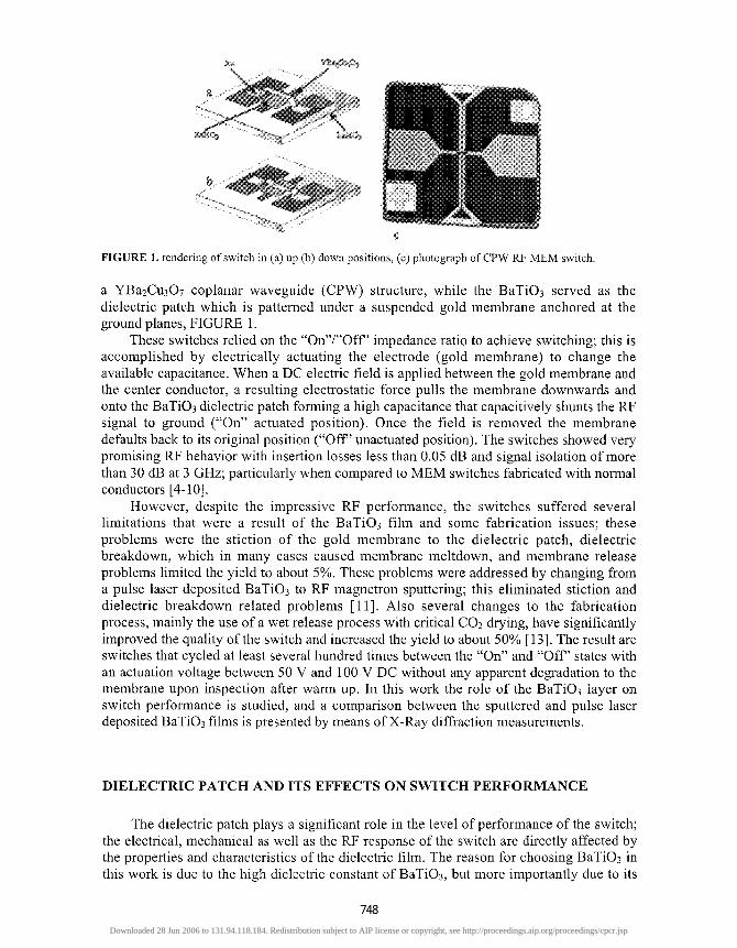
iFIGURE 1. rendering of switch in (a) up (b) down positions, (c) photograph of CPW RF MEM switch.
a YBaaCusOv coplanar waveguide (CPW) structure, while the BaTiOs served as thedielectric patch which is patterned under a suspended gold membrane anchored at theground planes, FIGURE 1.
These switches relied on the "On"/"Off ' impedance ratio to achieve switching; this isaccomplished by electrically actuating the electrode (gold membrane) to change theavailable capacitance. When a DC electric field is applied between the gold membrane andthe center conductor, a resulting electrostatic force pulls the membrane downwards andonto the BaTiO3 dielectric patch forming a high capacitance that capacitively shunts the RFsignal to ground ("On" actuated position). Once the field is removed the membranedefaults back to its original position ("Off unactuated position). The switches showed verypromising RF behavior with insertion losses less than 0.05 dB and signal isolation of morethan 30 dB at 3 GHz; particularly when compared to MEM switches fabricated with normalconductors [4-10].
However, despite the impressive RF performance, the switches suffered severallimitations that were a result of the BaTiOs film and some fabrication issues; theseproblems were the stiction of the gold membrane to the dielectric patch, dielectricbreakdown, which in many cases caused membrane meltdown, and membrane releaseproblems limited the yield to about 5%. These problems were addressed by changing froma pulse laser deposited BaTiOs to RF magnetron sputtering; this eliminated stiction anddielectric breakdown related problems [11]. Also several changes to the fabricationprocess, mainly the use of a wet release process with critical COi drying, have significantlyimproved the quality of the switch and increased the yield to about 50% [13]. The result areswitches that cycled at least several hundred times between the "On" and "Off states withan actuation voltage between 50 V and 100 V DC without any apparent degradation to themembrane upon inspection after warm up. In this work the role of the BaTiOs layer onswitch performance is studied, and a comparison between the sputtered and pulse laserdeposited BaTiOs films is presented by means of X-Ray diffraction measurements.
DIELECTRIC PATCH AND ITS EFFECTS ON SWITCH PERFORMANCE
The dielectric patch plays a significant role in the level of performance of the switch;the electrical, mechanical as well as the RF response of the switch are directly affected bythe properties and characteristics of the dielectric film. The reason for choosing BaTiOs inthis work is due to the high dielectric constant of BaTiOs, but more importantly due to its
Downloaded 28 Jun 2006 to 131.94.118.184. Redistribution subject to AIP license or copyright, see http://proceedings.aip.org/proceedings/cpcr.jsp
admin
748

compatibility with YE^CusO? and the overall fabrication process. Both the microscopicand macroscopic film properties will contribute to overall switch performance; these can bequantified by the crystal structure of the film, the relative dielectric constant er, and the filmsurface roughness.
Once the membrane collapses onto the dielectric patch, a flat interface between thedielectric patch material and the membrane material must exist, otherwise attractive forcesarising from film surface irregularities will hinder the membrane to default back, under itsintrinsic stress, to its original position. Surface roughness will also reduce the switchingspeed, particularly when the switch goes from the actuated to the unactuated position, andwill degrade the lifetime of the switch. Thus an important requirement for the dielectricpatch is to have a smooth surface such that the interface between the dielectric patch andgold membrane is maximally flat. A smooth surface will also improve the profile of thegold membrane since this profile will depend upon the underlying sacrificial layer (PMGI),which in turn depends on the underlying profile of the transmission line and dielectriclayer.
As discussed earlier, the capacitively shunted RF MEM switch relies on the ratio of"On" to "Off capacitance, when the membrane is unactuated the resulting capacitance isthat of the air gap and is very small; however once the membrane collapses the dominantcapacitance is that due to the dielectric layer only, and thus maximizing the capacitancewill increase the switch's ability to pass or shunt the RF signal. Accordingly the upper limitof this dielectric-induced capacitance will be determined primarily by the material relativedielectric constant and hence its crystal structure. The "On" and "Off capacitances can becalculated as follows:
___ (1)h*Cdie £QA £0£JieA
r - £^die o\^ON - 7 \A)
where _dte is the relative dielectric constant of the patch, hg is the gap height, hd is thedielectric thickness, and A is the actuation area. From equation 2 it can be seen that thevalue of the "On" capacitance is directly proportional to the dielectric constant and area,and is inversely proportional to the dielectric thickness. Hence, maximizing the dielectricconstant of the material and the capacitor area while minimizing the dielectric thicknesswill increases the value of the "On" capacitance. However; it is important to point out twodesign trade offs that must be taken into account: (1) Since decreasing the dielectricthickness will in turn decrease the breakdown voltage of the material, a minimum thicknessmust be maintained to ensure durability and resistance to dielectric breakdown. (2)Increasing the capacitance through area increase can only be accomplished by changing thewidth of the actuating gold membrane since the width of the transmission line, and hencethe effective dielectric patch area, is fixed for a 50 Q characteristic line impedance. Alsoincreasing the capacitance area will have a negative effect on the insertion loss in the "Offposition.
Downloaded 28 Jun 2006 to 131.94.118.184. Redistribution subject to AIP license or copyright, see http://proceedings.aip.org/proceedings/cpcr.jsp
admin
749
DEPOSITION OF BATIO3
Pulse Laser Deposition of BaTiO3
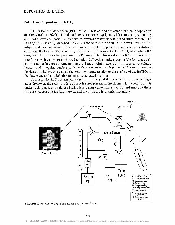
The pulse laser deposition (PLD) of BaTiOs is carried out after a one hour depositionof YBa2CusO7 at 760°C. The deposition chamber is equipped with a four-target rotatingarm that allows sequential depositions of different materials without vacuum breach. ThePLD system uses a Q-switched NdYAG laser with X = 532 nm at a power level of 300mJ/pulse; deposition system is depicted in figure 2. The deposition starts after the substratecools slightly from 760°C to 680°C, and takes one hour in 220mTorr of O2 after which thesample cools to room temperature in 200 Torr of 62. This results in a 0.5 ^im thick film.The films produced by PLD showed a highly diffractive surface responsible for its grayishcolor, and surface measurements using a Tencor Alpha-step 100 profilometer revealed abumpy and irregular surface with surface variations as high as 0.25 |im. In earlierfabricated switches, this caused the gold membrane to stick to the surface of the BaTiOs inthe downstate and not default back to its unactuated position.
Although the PLD system produces films with good thickness uniformity over largerareas; however, the relatively large particle sizes present in the plasma plume results in thisundesirable surface roughness [12]. Ideas being contemplated to try and improve thesefilms are: decreasing the laser power, and lowering the laser pulse frequency.
FIGURE 2. Pulse Laser Deposition system and plasma plume.
Downloaded 28 Jun 2006 to 131.94.118.184. Redistribution subject to AIP license or copyright, see http://proceedings.aip.org/proceedings/cpcr.jsp
admin
750

FIGURE 3. Two-target RF Magnetron Sputtering Setup.
RF Magnetron Sputtering of BaTi03
As for the magnetron sputtering of BaTi03 these films were sputtered on-axis at 36°C in 260 mTorr of Argon, with 80 Watts of forward RF power for three hours, FIGURE 3 depicts the RF magnetron sputtering process. The resulting films measured a thickness of 0.3 pm, obtained using ellipsometry, and demonstrated a translucent, almost transparent, smooth surface. A disadvantage of RF sputtering is its inability to produce uniform films even on areas as small as 15x15 mm2; however since the dielectric patch area occupies a very small portion of this surface area (0.18x0.8 mm'), film uniformity issues become irrelevant.
Experimental depositions in the presence of small percentages of 0 2 were carried out in attempts to increase the 0 2 content revealed damaging to the YBazCu307 film, this was due to the ionization of the 0 2 which is then accelerated in the RF plasma towards the sample resulting in back sputtering of the YBazCu307 film.
Switches fabricated with sputtered instead of pulse laser deposited BaTi03 showed similar RF performance [2,3]; however the problem of membrane stiction was practically eliminated with the switches cycling several hundred times or more with no apparent degradation to the gold membrane upon inspection after warm up.
X-RAY DIFFRACTION RESULTS
Three samples were prepared to investigate the crystal structure of the sputtered versus the pulse laser deposited films; one has a film of YBazCu307 only, while the other two samples have a BaTi03 film deposited on top of the YBa2Cu307 by PLD and sputtering, respectively. The results of the X-Ray diffraction patterns revealed that the YBa~Cu307 is predominantly c-axis orientation, with some a-axis growth also observed, FIGURE! 4. This confirms that the superconducting film has good crystal structure and is epitaxial.
The PLD deposited BaTi03 film exhibited some epitaxy with the underlying YBazCu307 film, FIGURE 5 , while the sputtered film had no signs of epitaxial growth, FIGURE 6. This is not surprising since the PLD deposition is carried out at 680°C versus 36°C for sputtering, this elevated temperature allows some of the BaTi03 crystals to align in prefered crystal directions.
Downloaded 28 Jun 2006 to 131.94.118.184. Redistribution subject to AIP license or copyright, see http://proceedings.aip.org/proceedings/cpcr.jsp
admin
751

FIGURE 4. X-Ray Diffraction Pattern for LaA103 and YBazCqO, Film.
FIGURE 5. X-Ray Diffraction Pattern for LaA103, YBazCu307 and PLD BaTi03 Film.
However, it is believed that this epitaxial growth is very limited due to the relatively large chunks ablated by the laser off of the BaTi03 target. These results also tell us that the dielectric behavior of the two films might also be quite different since one has completely random crystal orientation while the other has a level of preferred crystal orientations. The reason for this difference arises from the fact that BaTi03 is anisotropic and the material polarization in one crystal direction is different from other directions. This difference in behavior may become significant when talking about tunable applications.
Downloaded 28 Jun 2006 to 131.94.118.184. Redistribution subject to AIP license or copyright, see http://proceedings.aip.org/proceedings/cpcr.jsp
admin
752
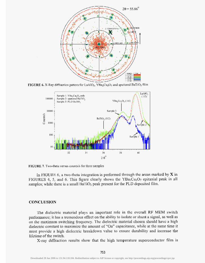
FIGURE 6. X-Ray diffraction pattern for LaA103, YBa2Cu307 and sputtered BaTiO3 film
LaAIO, (112)
- Sample 1: YB%C%O, only 100000 : Sample 2: sputtered BaTiO,
i Sample 3: PLD BaTiO, yB~cu,o,("" '
10000 7 Sample 3 \ - r
u 1000: BaTiO, (112)
I '
w 52 54 56
2 eo 5 8 60
FIGURE 7. Two-theta versus countds for three samples
In FIGURE 6 , a two-theta integration is performed through the areas marked by X in FIGURES 4, 5, and 6. This figure clearly shows the YBa2Cu307 epitaxial peak in all samples; while there is a small BaTi03 peak present for the PLD deposited film.
CONCLUSION
The dielectric material plays an important role in the overall RF MEM switch performance; it has a tremendous effect on the ability to isolate or shunt a signal, as well as on the maximum switching frequency. The dielectric material chosen should have a high dielectric constant to maximize the amount of "On" capacitance, while at the same time it must provide a high dielectric breakdown value to ensure durability and increase the lifetime of the switch.
X-ray diffraction results show that the high temperature superconductor film is
Downloaded 28 Jun 2006 to 131.94.118.184. Redistribution subject to AIP license or copyright, see http://proceedings.aip.org/proceedings/cpcr.jsp
admin
753
predominantly c-axis oriented and has good epitaxy with the underlying LaAlOs substrate.While some observation of epitaxy in the PLD BaTiOs deposited film was observed;however it is believed that this is not sufficient to cause a significant change in the value ofthe relative dielectric constant and therefore the RF performance was not significantlyaffected.
The PLD deposition resulted in a rough and irregular film and displayed limitedepitaxial growth. It is believed that the film may be improved by reducing the laser powerand pulse frequency, also reducing the laser wavelength might help decrease the size ofablated particles in the plasma plume. The roughness and irregularity of the PLD depositedfilm was responsible for poor performance in earlier switches; causing problems withstiction and dielectric breakdown. However, the RF magnetron sputtered BaTiOs film has asmooth surface with no film epitaxy; this eliminated earlier problems and proved superiorfor use in superconducting RF MEM switches.
ACKNOWLEDGEMENTSThis work was supported by the U.S. Air Force office of scientific Research under
grant number F49620-02-1-0044 and F49620-00-1-0379
REFERENCES1. Chang, L. H., Anderson, W. A. and Jia Q. X., J. Material Research 9, p. 2561 (2000).2. Hijazi, Y. S., Vlassov, Y. A. and Larkins, G. L., IEEE Trans. Appl. Supercond. 13, pp. 696-699 (2003).3. Hijazi, Y. S., Hanna, D., Fairweather, D., Vlasov, Y. A. and Larkins, G. L., IEEE Trans. Appl.
Supercond. 13, pp. 700-703 (2003).4. Rebeiz, G. M. and Muldavin, J., IEEE Microwave Trans., 2001, pp. 59-71.5. Park, J. Y., Kirn, G. H. and Chung K., Sensors and Actuators A 89, pp. 88-94 (2001).6. Muldavin, J. B. and Rebeiz, G. M., IEEE Trans. Microwave Theory Tech. 48, pp. 1045-1052 (2000).7. Pacheco, S., Nguyen, C. T. and Katehi, L. B., "Micromechanical electrostatic K-band switches", in
Proc. IEEE MTT-S International Microwave Symposium, Baltimore, Md, 1998, pp. 1569-1572.8. Pacheco, S. P., Katehi, L. P. B. and Nguyen, C. T.-C., "Design of Low Actuation Voltage RF MEMS
Switch", m IEEE MTT-S Int. Microwave Symposium Digest, 1, 2000, pp. 165-168.9. Yao, Z. J., Chen, S., Eshelman, S., Denninston, D. and Goldsmith C., "Micromachined Low-Loss
Microwave Switches", in J. Microelectromech. Syst., 8, no. 2, 1999, pp. 129-134.10. Muldavin, J. B. and Rebeiz G. B., "30 GHz Tuned Mems Switches", in IEEE MTT-S Int. Microwave
Symposium Digest, 4, 1999, pp. 1511-1514.11. Hijazi, Y., Martinez, J., Noel, J., Brzhezinskaya, M., Sayed, S., Vlasov, Yu., Larkins, G., "Improved
Superconducting RF MEM Switch", in Book of abstracts ofEUCAS 2003, Sorrento, Italy, 2003, p. 141.12. Chrisey, D. B. and Hubler, G. K., Pulsed Laser Deposition of Thin Film, Wiley, John & Sons, Inc.,
1994, ch. 4.13. Noel, J., Hijazi, Y., Martinez, J., Vlasov, Yu. A. and Larkins G. L., Supercond. Sci. Technol. 16, pp.
1438-1441 (2003).
Downloaded 28 Jun 2006 to 131.94.118.184. Redistribution subject to AIP license or copyright, see http://proceedings.aip.org/proceedings/cpcr.jsp
admin
754