Manipulation of magnetism in iron oxide nanoparticle / BaTiO3 ...
167
Schlüsseltechnologien / Key Technologies Band / Volume 180 ISBN 978-3-95806-351-8 Manipulation of magnetism in iron oxide nanoparticle / BaTiO 3 composites and low-dimensional iron oxide nanoparticle arrays Li-Ming Wang
-
Upload
khangminh22 -
Category
Documents
-
view
1 -
download
0
Transcript of Manipulation of magnetism in iron oxide nanoparticle / BaTiO3 ...

Schlüsseltechnologien / Key TechnologiesBand / Volume 180ISBN 978-3-95806-351-8
Schlüsseltechnologien / Key TechnologiesBand / Volume 180ISBN 978-3-95806-351-8
Manipulation of magnetism in iron oxide nanoparticle / BaTiO3 composites and low-dimensional iron oxide nanoparticle arraysLi-Ming Wang
180
Schl
üsse
ltech
nolo
gien
Ke
y Te
chno
logi
esN
anop
artic
le M
agne
to-E
lect
rics
Li-M
ing
Wan
g

Schriften des Forschungszentrums JülichReihe Schlüsseltechnologien / Key Technologies Band / Volume 180


Forschungszentrum Jülich GmbHJülich Centre for Neutron Science (JCNS)Quantenmaterialien und kollektive Phänomene (JCNS-2 / PGI-4)
Manipulation of magnetism in iron oxide nanoparticle / BaTiO3 composites and low-dimensional iron oxide nanoparticle arrays
Li-Ming Wang
Schriften des Forschungszentrums JülichReihe Schlüsseltechnologien / Key Technologies Band / Volume 180
ISSN 1866-1807 ISBN 978-3-95806-351-8

Bibliografische Information der Deutschen Nationalbibliothek. Die Deutsche Nationalbibliothek verzeichnet diese Publikation in der Deutschen Nationalbibliografie; detaillierte Bibliografische Daten sind im Internet über http://dnb.d-nb.de abrufbar.
Herausgeber Forschungszentrum Jülich GmbHund Vertrieb: Zentralbibliothek, Verlag 52425 Jülich Tel.: +49 2461 61-5368 Fax: +49 2461 61-6103 [email protected] www.fz-juelich.de/zb Umschlaggestaltung: Grafische Medien, Forschungszentrum Jülich GmbH
Druck: Grafische Medien, Forschungszentrum Jülich GmbH
Copyright: Forschungszentrum Jülich 2018
Schriften des Forschungszentrums JülichReihe Schlüsseltechnologien / Key Technologies, Band / Volume 180
D 82 (Diss., RWTH Aachen University, 2018)
ISSN 1866-1807ISBN 978-3-95806-351-8
Vollständig frei verfügbar über das Publikationsportal des Forschungszentrums Jülich (JuSER)unter www.fz-juelich.de/zb/openaccess.
This is an Open Access publication distributed under the terms of the Creative Commons Attribution License 4.0, which permits unrestricted use, distribution, and reproduction in any medium, provided the original work is properly cited.

II
Zusammenfassung
Es wurden ferrimagnetische Eisen-Sauerstoff Nanopartikel (NP) auf ferroelek-trischen BaTiO3-Substraten (BTO) hergestellt. An diesen Hererostruktren konnteeine magnetoelektrische Kopplung (MEC) festgestellt werden. Zuerst wurde eineEinzelschicht von Eisen-Sauerstoff NP durch Selbstorganization auf einem BTOEinkristallsubtrat aufgebracht. Durch Rontgenstreuung unter streifendem Einfall(GISAXS) und Rasterelektronenmikroskopie (SEM) wurde gezeigt, dass die NPEinzelschicht eine dicht gepackte hexagonale Struktur aufweist. Der MEC Ef-fect konnte durch Einbringen einer Ti-Schicht und Bedecken mit einer Au-Schichtverstarkt werden. Die Raster-Transmissionselektronenmikroskopie (STEM) lieferteInformationen uber die Schichtstruktur der Probe. Die Magnetisierung zeigt scharfeSprunge bei den Phasenubergangen des BTO-Stubtrats.
Die Manipulation der Magnetisierung durch elektrische Felder wurde mit einersupraleitenden Quanteninterferenzeinheit (SQUID) mit eingebautem elektrischemFeld durchgefuhrt. Die Magnetisierung aufgetragen gegen das DC elektrische Feldhat eine Schmetterlingsform und stimmt mit der piezoelektrischen Reaktion desBTO Einkristalls uberein. Dies bestatigt, dass der MEC hauptsachlich durch dieGrenzflachenspannungen ubermittelt wird. Das Signal der magnetoelektrischen ACSuszeptibilitat (MEASCS) als Funktion der Temperatur bei angelegtem AC elek-trischen Feld zeigt Sprunge bei den BTO Phasenubergangen.
Das magnetische Tiefenprofil der NP Einfachschicht bei variierten angelegtenDC elektrischen Feldern wurde von den Ergebnissen der polarisierten Neutronen-reflektometrie (PNR) abgeleitet. Die Unterschiede bei den Reflektometriekurvenwerden hauptsachlich durch die strukturellen Anderungen des Substrates und derEinzelschichten hervorgerufen. Zusatzlich hat die veranderte Magnetisierung derNP Einzelschichten einen kleineren Effekt auf die Unterschiede in den Reflektome-triekurven.
Es wurden zusatzlich selbstorganisierte Eisen-Sauerstoff NP auf einer BTO-Schicht auf einem Nb dotiertem SrTiO3 Substrat (Nb doped STO) hergestellt. An-dererseits deuteten die Messungen der Magnetisierung als Funktion des DC elek-trischen Feldes und die MEACS Resultate an, dass ein MEC zwischen NP und derBTO-Schicht vorliegt. Oberflachenladungen und Spannungsubertragungen an derGrenzschicht sind fur den MEC verantwortlich.
Zusatzlich wurden selbstorganisierte NP in lateral strukturierten Silizium-Substraten(Si) hergestellt um die magnetische Anisotropie und das kollektive magnetische Ver-halten zu untersuchen. Die Magnetisierung als Funktion des magnetischen Feldeszeigt einen großen strukturinduzierten magnetischen Anisotropieeffekt. Die Resul-tate der Elektronenholographie, nach dem Anlegen eines magnetischen Sattigungsfeldesentlang der lateralen Strukturen, zeigen, dass ein geordneter magnetischer Zustandin den NP-Anordnungen existiert. Die NP zeigen einen ferromagnetisch (FM) geord-neten Zustand und einen kleinen Memory-Effekt entlang der lateralen Strukturenan. Senkrecht zu den lateralen Strukturen wird aber ein großer Memory-Effekt

III
beobachtet. Wir folgern daraus, dass der FM geordnete Zustand den Superspin-Glas Zustand der dipolar gekoppelten NP unterdruckt.
Diese Arbeit eroffnet viele Moglichkeiten fur energieeffiziente elektronische Bauteilehergestellt durch einfache Selbstanordnungstechniken.

IV
Abstract
Ferrimagnetic (FiM) iron oxide nanoparticles (NPs) on top of ferroelectric BaTiO3
(BTO) substrates were prepared and a magnetoelectric coupling (MEC) effect wasobserved in the heterostructures. Iron oxide NPs first were self-assembled as amonolayer on top of BTO substrates. Grazing incidence small angle x-ray scat-tering (GISAXS) and scanning electron microscopy (SEM) confirm a close-packedhexagonal order of the NP monolayers. By inserting a Ti layer and further cappingwith an Au layer, an enhanced MEC effect was observed. Scanning transmissionelectron microscopy (STEM) provides information about the layer structure of thesample. The magnetization shows sharp magnetization jumps at the phase transi-tion temperatures of the BTO substrate.
Electric field manipulation of magnetism was performed using a superconductingquantum interference device (SQUID) setup with an electric field implemented. Abutterfly shaped curve of the magnetic moment vs. DC electric field was obtainedwhich is coincident with the piezoelectric response of BTO single crystals whichconfirms a strain mediated MEC. The magnetoelectric ac susceptibility (MEACS)signal as function of temperature under an AC electric field shows abrupt jumps atthe BTO phase transition temperatures.
The magnetic depth profiles of NP monolayers at various applied DC electricfields were deduced from polarized neutron reflectivity (PNR) results. Fitting ofthe data shows that the observed differences in reflectivity curves are caused by thechanged structural properties of the substrate and layers as a major factor and thealtered magnetism of NP monolayers as a minor factor.
Also iron oxide NPs self-assembled on BTO films on Nb doped SrTiO3 (Nbdoped STO) substrates were prepared. The DC electric field vs. magnetizationand MEACS results indicate that there is a MEC between NPs and the BTO film.Interface charge and strain transfer are responsible for the MEC effects.
Moreover, NPs self assembled into trench-patterned silicon (Si) substrates wereprepared to investigate the magnetic anisotropy and collective magnetic behav-ior. The magnetization vs. magnetic field shows a large shape-induced magneticanisotropy effect. After the application of a magnetic saturation field along thetrenches, electron holography results show that an overall magnetic ordered stateexists in the nanoparticle assemblies. In the direction of the trenches, the NPsexhibit a ferromagnetic (FM) -like ordered state and a small memory effect wasobserved. Whereas large memory effect was observed perpendicular to the trenches.We conclude that the FM ordered state suppresses a superspin glass state of thedipolarly coupled NP moments.
This work opens up viable possibilities for energy-efficient electronic devices fab-ricated by simple self-assembly techniques.


Contents
1 Introduction 1
2 Theoretical Background 52.1 Magnetic susceptibility . . . . . . . . . . . . . . . . . . . . . . . . . . 52.2 Magnetic interactions . . . . . . . . . . . . . . . . . . . . . . . . . . . 5
2.2.1 Magnetic dipolar interaction . . . . . . . . . . . . . . . . . . . 52.2.2 Exchange interaction . . . . . . . . . . . . . . . . . . . . . . . 6
2.3 Magnetic order . . . . . . . . . . . . . . . . . . . . . . . . . . . . . . 82.3.1 Ferromagnetism (FM) . . . . . . . . . . . . . . . . . . . . . . 82.3.2 Antiferromagnetism (AF) . . . . . . . . . . . . . . . . . . . . 92.3.3 Ferrimagnetism (FiM) . . . . . . . . . . . . . . . . . . . . . . 102.3.4 Spin glasses (SG) . . . . . . . . . . . . . . . . . . . . . . . . . 10
2.4 Magnetic anisotropy . . . . . . . . . . . . . . . . . . . . . . . . . . . 112.4.1 Magnetocrystalline anisotropy . . . . . . . . . . . . . . . . . . 112.4.2 Shape anisotropy . . . . . . . . . . . . . . . . . . . . . . . . . 122.4.3 Surface anisotropy . . . . . . . . . . . . . . . . . . . . . . . . 122.4.4 Strain anisotropy . . . . . . . . . . . . . . . . . . . . . . . . . 13
2.5 Superparamagnetism . . . . . . . . . . . . . . . . . . . . . . . . . . . 142.6 Iron oxides . . . . . . . . . . . . . . . . . . . . . . . . . . . . . . . . . 17
2.6.1 Wustite, FexO . . . . . . . . . . . . . . . . . . . . . . . . . . . 182.6.2 Magnetite, Fe3O4 . . . . . . . . . . . . . . . . . . . . . . . . . 192.6.3 Maghemite, γ-Fe2O3 . . . . . . . . . . . . . . . . . . . . . . . 192.6.4 Hematite, α-Fe2O3 . . . . . . . . . . . . . . . . . . . . . . . . 21
2.7 Ferroelectric and magnetoelectric materials . . . . . . . . . . . . . . . 212.7.1 Piezoelectric and ferroelectric materials . . . . . . . . . . . . . 212.7.2 Magnetoelectric systems . . . . . . . . . . . . . . . . . . . . . 24
2.8 Scattering methods . . . . . . . . . . . . . . . . . . . . . . . . . . . . 242.8.1 Basics of scattering methods . . . . . . . . . . . . . . . . . . . 252.8.2 Bragg scattering . . . . . . . . . . . . . . . . . . . . . . . . . 262.8.3 Grazing incidence scattering - Reflectometry . . . . . . . . . . 26
3 Methods and Instruments 313.1 NP self-assembly methods . . . . . . . . . . . . . . . . . . . . . . . . 313.2 Scanning Electron Microscopy (SEM) . . . . . . . . . . . . . . . . . . 323.3 Scanning Transmission Electron Microscopy (STEM) . . . . . . . . . 32
V
VI CONTENTS
3.4 Atomic Force Microscopy (AFM) . . . . . . . . . . . . . . . . . . . . 333.5 Piezoresponse Force Microscopy (PFM) . . . . . . . . . . . . . . . . . 343.6 SQUID magnetometry . . . . . . . . . . . . . . . . . . . . . . . . . . 353.7 X-ray Reflectometry/Diffractometry (XRR, XRD) . . . . . . . . . . . 383.8 Grazing Incidence Small Angle X-ray Scattering (GISAXS) . . . . . . 393.9 Polarized neutron reflectometry (PNR) . . . . . . . . . . . . . . . . . 40
4 Results I: Iron oxide NPs on BTO single crystals 434.1 Sample preparation . . . . . . . . . . . . . . . . . . . . . . . . . . . . 43
4.1.1 BTO single crystals . . . . . . . . . . . . . . . . . . . . . . . . 434.1.2 NPs self-assembled on BTO . . . . . . . . . . . . . . . . . . . 474.1.3 BTO / Ti / NP monolayers . . . . . . . . . . . . . . . . . . . 494.1.4 Au / BTO / Ti / NP monolayer / Au . . . . . . . . . . . . . 50
4.2 Results . . . . . . . . . . . . . . . . . . . . . . . . . . . . . . . . . . . 514.2.1 Macroscopic magnetic properties . . . . . . . . . . . . . . . . 514.2.2 Analysis of the magnetic depth profile . . . . . . . . . . . . . 664.2.3 Discussion and outlook . . . . . . . . . . . . . . . . . . . . . . 72
4.3 NP multilayers on BTO substrate . . . . . . . . . . . . . . . . . . . . 78
5 Results II: Iron oxide NPs on BTO films 815.1 Sample preparation . . . . . . . . . . . . . . . . . . . . . . . . . . . . 81
5.1.1 BTO thin films . . . . . . . . . . . . . . . . . . . . . . . . . . 815.1.2 Nb-doped STO / BTO / NP monolayers . . . . . . . . . . . . 855.1.3 Nb-doped STO / BTO / NP monolayers / BTO / Au . . . . . 86
5.2 Results . . . . . . . . . . . . . . . . . . . . . . . . . . . . . . . . . . . 865.3 Discussion and outlook . . . . . . . . . . . . . . . . . . . . . . . . . . 90
6 Results III: NPs self-assembled on patterned substrates 936.1 NPs / patterned sapphire substrates . . . . . . . . . . . . . . . . . . 936.2 NPs / patterned Si substrates . . . . . . . . . . . . . . . . . . . . . . 94
7 Summary and Outlook 105
8 Bibliography 109
List of Figures 121
List of Tables 133
List of Acronyms 134
Appendix 137
Acknowledgements 146

Chapter 1
Introduction
Magnetoelectric (ME) materials are systems where the magnetization can be ma-nipulated by electric field or the polarization can be tuned by magnetic field [1, 2].They have stimulated large research interest due to their potential applications inspintronics or multifunctional devices [3, 4, 5, 6]. For storage devices, ME arti-ficial heterostructures can combine the advantages of ferroelectric random accessmemories (FERAMs) and magnetic random access memories (MRAMs) [7, 8].
Moreover, the ability to switch the magnetization via an electric field in ME ma-terials could reduce the energy consumption to write data in electronic devices andalso offers the possibility to scale down MRAMs even further [7, 9, 8]. Single-phaseME systems are rare and most of them only show an ME effect at low tempera-ture or in a narrow temperature range [10, 11, 12, 13]. Alternatively, with greaterdesign flexibility, multiferroic ME composites fabricated by combining piezoelectricand magnetic materials have drawn significant interest in recent years due to theirmultifunctionality and a large ME response (i.e., several orders of magnitude largerthan in single-phase ME materials) [14, 15].
Recently, strain mediated ME coupling (MEC) effects were evidenced in variousthin film systems composed of a ferromagnetic (FM) Fe, SrRuO3 or La0.7Sr0.3MnO3
layer on top of a ferroelectric (FE) substrate, e.g. BTO or PbMg1/3Nb2/3O3 - PbTiO3
(PMN-PT). The coupling is manifested as a change of the magnetization or resis-tance at the structural phase transition temperatures of the ferroelectric subsys-tem [16, 17, 18, 19, 20]. These studies argue that the MEC effects are the result ofstrain-mediated coupling, partially strain and partially charge mediated or purelycharge-mediated coupling.
FM-FE or FiM-FE composites based on magnetic NPs are promising novel can-didates for artificial nanoscale multiferroic devices [21, 22]. For example, theycan be used for fabricating flexible electronics and provide the possibility of cost-efficient manufacturing via spin-coating or printing methods. A recent study showedthat switching of the magnetic properties of Ni nanocrystals between a super-paramagnetic (SPM) and a stable FM state by MEC to a FE substrate is possi-ble [23]. In addition, NPs can be considered as building blocks for artificial super-structures [24, 25, 26]. One prominent route is to employ the self-organization of
1

2 CHAPTER 1. INTRODUCTION
NPs into regular arrangements, so called ”supercrystalline lattices” or ”supercrys-tals” [27, 28]. Such systems are particularly interesting, because of their prospectiveapplications as multifunctional materials.
However, the understanding of ME systems including supercrystalline NP as-semblies is still very limited and consequently several open questions remain, e.g.what is the exact mechanism of MEC in such nanocomposites? How can it be tunedand optimized? Therefore, we investigate strain and electric field mediated MEC ina model system composed of a monolayer of self-assembled iron oxide NPs coupledto a BTO substrate.
Large-areas of NP arrangements with long-range order with a desired morphologyis an essential step to the fabrication of novel nanoelectronics, magnetoelectronics,biochemical sensors. The assembly of 1 or 2 dimensional (1D or 2D) nanoscalecolloidal structures are very promising for this purpose [29, 30, 31]. An efficientroute to prepare (pseudo-) 1D NP chains is the template-assisted fabrication [32,33, 34, 35]. These methods have been widely used to self-assemble metallic NPs intolong-range ordered pseudo-1D NP chains. For example, M. Kang et al. reported1D Au NP arrays encapsulated within free-standing SiO2 nanowires [36]. D. Xia etal. demonstrated directed self-assembly of silica NPs into nanometer-scale groovespatterned surfaces [30]. Although some FM / FiM NPs also was tried with themethods, Park and co-workers reported the assembly of iron oxide NPs into 200 nmchains using a bio-inspired template [34]. Nevertheless, the fabrication of long-rangorder (pseudo-) 1D FM / FiM NP chains across large areas are still challenging.
Besides applications, such NP arrangements also play critical roles in the un-derstanding of fundamental magnetism. Interparticle dipole-dipole interactions canlead to collective spin-glass ordering at low enough temperature. Interaction be-tween magnetic entities causes collective phenomena at low enough temperatures,provided the dimensionality of the system is above the lower critical dimension [37].Interacting magnetic nanoparticles can exhibit the same phenomenology as atomicspin glasses, namely superspin glass (SSG) state. Memory effect is the most sig-nificant feature of the SSG state and is widely accepted as the most direct andstraightforward criterion to judge whether it is a superspin glass state.
SSG systems have received much attention in recent years for their appealingnovel properties such as nonexponential relaxation, aging and memory effect [38,39, 40]. Among them, NP systems with dipole-dipole interactions (superspins, spinsin a single domain NP can be regarded as a superspin) are the most attractive SSGsystems to be investigated for their easy self-assembly methods and their attrac-tive properties. Magnetic anisotropy and the SSG state are investigated on lowdimensional iron oxide NPs in patterned substrates.
This thesis is structured as follows: a short theoretical background about mag-netism is given in chapter 2, it includes a description of various types of magneticinteractions and four types of magnetic orders which are most frequently mentionedin the following chapters. Afterwards, superparamagnetism is briefly explained toget a better understanding of the magnetic behavior of NPs. The structures andmagnetic behavior of the several basic iron oxides are illustrated in the next section.

3
The ferroelectric properties of BaTiO3 and the magnetoelectric materials are intro-duced afterwards. Since scattering methods are used extensively for the investigationof our system, the theoretical background of scattering methods are summarized.The experimental instruments are described in the chapter 3 to provide an overviewof the methods we used in our investigations. The results of the magnetic and struc-tural properties of NPs on different substrates are presented in chapter 4 to 6. Thediscussion on observed effects and the outlook for future investigations are given inchapter 7.

4 CHAPTER 1. INTRODUCTION

Chapter 2
Theoretical Background
2.1 Magnetic susceptibility
For magnetic materials, after applying an external magnetic field ~H, a magnetization(magnetic moment per volume) ~M is generally induced. In the simplest case of alinear and isotropic response, one can write:
~M = χ ~H (2.1)
where χ is the magnetic susceptibility. It is a dimensionless quantity. The magneticmaterials can roughly be distinguished in three classes. When χ<0, it is diamagnetic,when χ>0, it is paramagnetic and when χ1, it is ferromagnetic.
2.2 Magnetic interactions
In diamagnetism or paramagnetism for localized moments, the magnetic momentsare independent and very weak magnetic interaction exist. However, some solidscan show long range magnetic order. When the orientation of the moments pointsin the same direction, the system is known as ferromagnetic. When the orderingis alternating in opposite directions, it is known as antiferromagnetic. When theordering is in opposite directions but with different magnitudes of the sublatticemoments, it is known as ferrimagnetic. The various interactions will be brieflydiscussed in this section.
2.2.1 Magnetic dipolar interaction
Magnetic moments show dipole-dipole interactions amongst them. The energy be-tween two moments ~µ1 and ~µ2 separated by ~r is given by
Ed =µ0
4πr3[ ~µ1 · ~µ2 −
3
r2( ~µ1 · ~r)( ~µ2 · ~r)] (2.2)
The energy depends on the separation and the orientation of the moments. Theorder of magnitude for two atomic moments each of µ ≈ 1µB separated by 1 A isapproximately 10−23 J which is equivalent to about 1K in temperature.
5

6 CHAPTER 2. THEORETICAL BACKGROUND
As for nanoparticles, since the total moment is 106 times larger than atomicmoments, the dipolar ordering energy can be as large as thousands of Kelvin. Forexample, two iron oxide NPs with the diameter of 20 nm, has the moment µ of3.7×106 µB and a center to center separation of r = 20 nm, the energy scale isaround 2100 K.
2.2.2 Exchange interaction
The most significant interaction responsible for long-range magnetic order is ex-change interaction. The origin can be explained by taking into account the electro-static interaction between electrons.
The Pauli exclusion principle states that two or more fermions of the same kindcannot be in the same state. Hence, considering a simple system of two electrons,the overall wavefunction of the electrons must be antisymmetric. The wavefunctioncan be separated into a spatial part and a spin part. When the spin part is anti-symmetric, the spatial part must be symmetric (singlet state, S = 0) and vice versa(triplet state, S = 1).
The exchange constant J is defined as the energy difference between the tripletstate and singlet state.
J =ES − ET
2(2.3)
Hence, the spin-dependent term in the effective Hamiltonian can be expressedas
Hspin = −2J ~S1 · ~S2 (2.4)
If J > 0, the spatial wavefunction of the two electrons is antisymmetric, exchangeenergy favors electrons with parallel spins. If J < 0, the spatial part is symmetric,the interaction favors electrons with antiparallel spins.
However, in a many-body system, the Hamiltonian is written as
Hspin = −∑ij
Jij ~S1 · ~S2 (2.5)
where Jij is the exchange constant between the ith and jth spins. This is calledHeisenberg Hamiltonian.
The exchange interaction can be further subdivided into the following types.
Direct exchange
If electrons on neighboring magnetic atoms interact via an exchange interaction, thisis known as direct exchange. The exchange interaction proceeds directly without anintermediary. It gives a strong, but short range coupling which decreases rapidly asthe ions are separated.
Direct exchange interaction plays sometimes a role in NP self-assemblies, wherethe surfaces of the NPs are in close contact.

2.2. MAGNETIC INTERACTIONS 7
Indirect exchange: Superexchange
Indirect exchange interaction exists in several magnetic materials, e.g. in oxides orfluorides, as in MnO and MnF2. There the direct orbital overlap between Mn2+ ionsis not possible. The magnetic ions interact via a non-magnetic ion like oxygen. Suchan interaction is called superexchange interaction.
Indirect exchange: RKKY
In metals the exchange interaction between magnetic ions can be mediated by con-duction electrons. A localized magnetic moment polarizes the conduction electrons,which in turn couples to another localized magnetic ion and influences its magneticstate. This kind of indirect exchange is called Ruderman, Kittel, Kasuya and Yosida(RKKY) interaction. The coupling depends on the distance (hereby r k−1
F ) andis given by
JRKKY (r) ∝ cos(2kF r)
r3(2.6)
where r is the distance between the localized magnetic moments and kF is the radiusof the Fermi surface. The interaction is long range and oscillatory in nature. Theinteraction leads to FM and AF coupling depending on the distance.
Double exchange
In some solids, the magnetic ion can show mixed valency. Then it has the possibilityto show a FM interaction amongst the ions which is known as double exchange. E.g.in magnetite, in octahedral environment, due to the crystal field splitting effect, theFe d-orbital will split into eg and t2g level with the former level having higher energy.
Fe2+ Fe3+
[Ar]3d6 [Ar]3d5
3d
eg
t2g
3d
t2g
eg
Ferromagne!c
An!ferromagne!c
(a)
(b)
Figure 2.1: Double exchange interaction between octahedrally coordinated Fe2+
and Fe3+ in magnetite. (a) Electron hopping is allowed from Fe2+ to Fe3+ for fer-romagnetic alignment. (b) Forbidden electron hopping in case of antiferromagneticalignment due to the Pauli exclusion principle.

8 CHAPTER 2. THEORETICAL BACKGROUND
The configuration for Fe2+ and Fe3+ is shown in Figure 2.1. The electron hoppingbetween Fe2+ and Fe3+ leads to an effective FM interaction, because the electrondelocalization and a parallel spin alignment lowers the energy of the system. Hence,double exchange interaction leads to ferromagnetism.
2.3 Magnetic order
Depending on the interactions between magnetic moments, a solid can show varioustypes of long-range magnetic order.
2.3.1 Ferromagnetism (FM)
When the moments are parallel to each other in its ground state, then this system isknown as ferromagnet. A ferromagnet shows spontaneous magnetization in absenceof a magnetic field. This is the case when J > 0. In general one can write for asystem with exchange interactions in an applied magnetic field B,
H = −∑ij
Jij ~Si · ~Sj + gµB∑j
~Sj · ~B (2.7)
where ~S is the spin vector operator. The first term is the Heisenberg exchangeitem while the second term is the Zeeman item. The exchange constants Jij for thenearest neighbors are positive for the case of ferromagnetic alignment.
The Weiss model is used to explain the origin of FM. In this model, the interac-tion between the moments is treated in such a way that each moment experiencesa mean field (or ”molecular field”). After neglect the thermal fluctuation effect, theeffective mean field is given by
~Bmf = λ ~M (2.8)
where λ is a constant known as Weiss coefficient and ~M is the magnetization. We arenow able to treat the problem as a paramagnet placed in a magnetic field ~B+ ~Bmf . Atlow temperatures, the moments are aligned by the internal mean field even withoutexternal magnetic field. As the temperature increases, thermal fluctuations beginto gradually destroy the aligned moments and finally at a critical temperature, theorder becomes destroyed.
The susceptibility of ferromagnet is expressed as,
χ ∝ 1
T − TC(2.9)
Where TC is the so-called Curie temperature. This is known as the Curie-Weisslaw [41].

2.3. MAGNETIC ORDER 9
2.3.2 Antiferromagnetism (AF)
If the exchange interaction is negative, J < 0, the magnetic moments are alignedantiparallel to the nearest neighbors. This is called antiferromagnetism. Usually,it is considered as two interpenetrating sublattices (see Figure 2.2). One sublatticewith all moments pointing up and the other with all moments pointing down. If we
Figure 2.2: Antiferromagnetic moments configuration can be decomposed into twointerpenetrating sublattices.
label the ’up’ sublattice + and the ’down’ sublattice -, then similar to a ferromagnet,the molecular field can be written as
B+ = −|λ|M− (2.10)
B− = −|λ|M+ (2.11)
The magnetization of each sublattice can be written as
M± = MsBj(gJµBJ |λ|M∓
kBT) (2.12)
The magnitude of the sublattices magnetizations are herby equal.
| ~M+| = | ~M−| = |M | (2.13)
Analogous to the ferromagnet one can solve it as mean field problem and arrives at
χ ∝ 1
T − θ(2.14)
where θ is the Weiss temperature. If θ = 0, the material is paramagnetic, thematerial is FM, if θ > 0, if θ < 0, the material is a antiferromagnetic (AF).
There is a phase transition between AF to paramagnetic state, the temperaturefor the phase transition is called Neel temperature (TN) [42].
The temperature dependence of the susceptibilities parallel and perpendicularto the easy axis are shown in Figure 2.3.

10 CHAPTER 2. THEORETICAL BACKGROUND
Figure 2.3: Temperature dependence of the susceptibility of an antiferromagnet forsusceptibilities parallel and perpendicular to the easy axis. Taken from Ref. [42]
2.3.3 Ferrimagnetism (FiM)
If the two sublattices as described in the antiferromagnet have different magnitudesof the magnetic moment, |M+| 6= |M−|, then the sublattices can not cancel out anda net magnetization is expected. This is known as Ferrimagnetism (FiM).
Magnetite (Fe3O4) is a typical FiM material containing an equal mixture of Fe2+
and Fe3+ ions on octahedral sites, together with the same number of Fe3+ ions ontetrahedral sites. The Fe2+ and Fe3+ ions on octahedral sites are parallel aligned,the Fe3+ ions on the tetrahedral sites are antiparallel aligned to the Fe3+ ions onoctahedral sites. Hence the net magnetization from all Fe3+ ions is zero and leave anet moment due to the Fe2+ ions alone. Magnetite shows a TC at 858 K.
2.3.4 Spin glasses (SG)
Spin glasses (SG) are magnetic systems in which no conventional long-range ordercan be established. However, they exhibit a freezing transition to a state withnew kind of order in which the spins are oriented in random directions [43]. Thistemperature is called SG transition temperature Tg.
The SG state can be induced when spin fullfills the both conditions of disorderand frustration. The disordered spins can be induced by position disorder andanisotropy disorder while the their frustration can be induced from RKKY effect ordipole-dipole interaction [44].
The most familiar and well studied SG systems are the dilute magnetic alloyssuch as AuFe, AgMn and CuMn, so-called canonical SG [45, 46, 47]. The localizedmoments of randomly distributed magnetic moments interact with each other viathe s−d exchange interaction mediated by the conduction electrons, the RKKY in-teraction. The oscillating nature of the RKKY interaction with distance, combinedwith spatially random arrangement of localized moments, gives rise to frustrationand randomness. With the neglect of spin anisotropy, the canonical SG is well de-scribed by the three-dimensional (3D) Heisenberg model [48]. For example, AuFe,Fe 8 at.%, Fe substitutes few sites in non magnetic Au lattice in a random distri-bution, then the system shows a disordered state. The temperature dependence ofboth Hall resistivity and magnetization show a cusp at Tg and the ZFC and FC

2.4. MAGNETIC ANISOTROPY 11
hysteresis below Tg [45].Analogously to the SG state in bulk materials, interacting single-domain NPs
also show such state which is called superspin glass (SSG) state. Due to the largemagnetic moments of NPs (superspins), the dipole–dipole interaction is considerablein closely packed nanoparticles assemblies [40, 49, 50].
2.4 Magnetic anisotropy
An important energy contribution determines the direction of spontaneous magne-tization in a magnetic material, which is known as the magnetic anisotropy. Oneobserves two different directions in the materials, known as easy axis and hard axis.Along the easy axis, it is easy to magnetize the material, and during a magneti-zation reversal process, a smaller magnetic field is required. For determining theoverall anisotropy in a bulk material, magnetocrystalline anisotropy and magneto-static demagnetization should be taken into consideration in the first place, whilein nanostructures, the shape, surface and strain anisotropy need to be consideredpreferentially [24].
2.4.1 Magnetocrystalline anisotropy
Magnetic moments in a crystal are in an environment of a periodic lattice. Thewavefunctions of neighboring moments exhibit different overlap energies for variedorbital moment orientations, which together with the spin-orbit interaction is thecause of magnetocrystalline anisotropy. Along certain crystallographic directions,it is easy to magnetize the crystal. In some cases, crystallographic directions arepreferred over shape, surface and any other effects for the orientation of the magne-tization.
For a hexagonal lattice, the easy axis is along the c-axis of the unit cell, whichis known as uniaxial anisotropy. The energy associated with it is expressed as
Euni = Ku1V sin2φ+Ku2V sin
4φ+ ...... (2.15)
where Ku1, Ku2 etc. are the anisotropy constants, V is the volume and φ is the anglebetween the easy axis and magnetic moment direction. The anisotropy constantsshow a strong temperature dependency, however, it can be regarded as a constantwhen the temperature is well below TC . In most cases, Ku1 is, by far, larger thanthe following terms and hence, the higher order terms can be neglected. Hence, themagnetocrystalline anisotropy energy can be simplified to Euni = Ku1V sin
2φ. Itcan be seen that, to switch the magnetic moments, one has to overcome an energybarrier ∼ Ku1V .
For a cubic system, the anisotropy is expressed as
Ecubic = K1(1
4sin2θsin22φ+ cos2θ)sin2θ +
K2
16sin22φsin22θsin2θ + ... (2.16)
where θ and φ are the polar and azimuthal angles between the favored direction andthe magnetic moment, respectively.

12 CHAPTER 2. THEORETICAL BACKGROUND
2.4.2 Shape anisotropy
The shape of the material also creates an additional anisotropy due to the demag-netization energy. A magnetized body produces magnetic ”charges” or poles at thesurface. This surface charge distribution is itself another source of a magnetic field,called the demagnetizing field. This will act in opposition to the magnetization thatproduces it. The demagnetization energy can be written as
Edm = −µ0
2
∫~M · ~HdmdV (2.17)
where ~M is the magnetization and ~Hdm is the demagnetization field. A sphericalbody has zero shape anisotropy. However, in a ellipsoidal body, the demagnetizingenergy is smaller if the magnetization lies along the long axis than along the shortaxes. Hence, it produces an easy axis of magnetization along the long axis. Thedemagnetization energy of a magnetized ellipsoid is given by
Edm =1
2V µ0M
2Ssin
2θ(N⊥ −N‖) (2.18)
where MS is the saturation magnetization of the material, θ is the angle betweenlong axis and the direction of MS. N‖ and N⊥ are the demagnetization factors,parallel or perpendicular with respect to the long axis of the ellipse, respectively.Both factors are a function of the ellipticity k of the particles as
N‖ =1
k2 − 1
(k
2√k2 − 1
ln(k +√k2 − 1
k −√k2 − 1
)− 1)
)(2.19)
N⊥ =k
2(k2 − 1)
(k − 1
2√k2 − 1
ln(k +√k2 − 1
k −√k2 − 1
)
)(2.20)
The demagnetization factors always satisfy the condition N‖ + 2N⊥ =1 [51]. Themagnitude of shape anisotropy depends on the saturation magnetization.
2.4.3 Surface anisotropy
Atoms at the surface are unsaturated, which leads to an enhancement of the anisotropyenergy. Especially in reduced dimensional systems, surface anisotropy plays a dom-inant role over magnetocrystalline anisotropy and magnetostatic energies. In caseof small spherical particles, the effective magnetic anisotropy can be written as
Keff = KV +S
VKS = KV +
6
dKS (2.21)
where S = πd2 and V = πd3/6 are the surface and volume of the particles. S/V isthe ratio of surface to volume, and d is the diameter of the particle. KV and KS arethe volume and surface anisotropies, comprising the terms of magnetocrystalline,shape and magnetostriction terms, respectively [52, 53]. A simulated spin structurein dependence of KV and KS is depicted in Figure 2.4.

2.4. MAGNETIC ANISOTROPY 13
Ks/Kv=1, spin in-surface Ks/Kv=10 Ks/Kv=60, spin out-surfaceKs/Kv=40
Figure 2.4: Spin structure from Monte-Carlo simulation of FePt NPs. The spinstructures are collinear along the in-plane direction, when the ratio of surfaceanisotropy to volume anisotropy is equal. As the surface anisotropy becomes largerthan the volume anisotropy, spins are canted away from the in-plane direction andtend to lie outward or inward. Taken from Ref [54].
The surface anisotropy can exert a strong influence on the magnetic structureof magnetic nanoparticles. In sufficiently small particles, there is a sharp cross-overfrom a throttled spin structure, where the core spins are parallel to each other andwhere the outermost spins tend to lie normal to the surface, forming a hedgehogstructure where all the spins are radially oriented either inward or outward, givinga net magnetization close to zero.
2.4.4 Strain anisotropy
Strain anisotropy arises from the strain dependence of the anisotropy constants. It isoften interpreted by the magnetostriction effect, which is a change in the material’sphysical dimensions as a result of the change in orientation of the magnetization.Usually, the relative deformation is very small, in the order of 10−5 to 10−6 [55].An uniaxial stress can produce an unique easy axis of magnetization, if the stressis sufficient to overcome all the other anisotropies. The magnitude of the strainanisotropy is often described by two empirical constants, known as the magne-tostriction constants, (λ111 and λ100), and the magnitude of stress σ. For example,in a cubic system, the magnetostriction constant along [110] can be a linear combi-nation of λ111 and λ100. For an isotropic magnetostriction (i.e. in iron oxide NP),λ111 = λ100 = λ [56].
The way in which a material responds to stress depends on its saturation magne-tostriction λs. For this analysis, the compressive stress σ is considered as negative,whereas the tensile stress is positive.
In the case of a single stress σ acting on a single magnetic domain, the magneticstrain anisotropy energy E can be expressed as
E =3
2λsσsin
2θ (2.22)
where θ is the angle between the measured magnetic moment and the σ-axis. Theeffect of stress on the isotropic sample depends on the sign of the σλS product.

14 CHAPTER 2. THEORETICAL BACKGROUND
( b )( a ) ( c )
Figure 2.5: (a) A ferromagnetic body with 90 degree domains. (b) Tensile straindecreases the magnetic moments in domains perpendicular to the stress direction.(c) Higher stress leaves only magnetic moments parallel to the stress direction.
Stress applied to a multi-domain ferromagnetic body will affect the orientationof magnetization through magnetostriction [57]. An example of the stress on themagnetization reversal of a Ni sample is given in the Figure 2.5. Hereby, the σλS ispositive for Ni. The application of tensile stress causes the domains with magneticmoments perpendicular to the stress to dwindle, as shown in Figure 2.5(b). Asthe strength of the tensile stress increases, the domains perpendicular to the stressvanish and leave only the magnetic moments parallel to the stress. If compressivestress was applied instead, the vertical domains would disappear accordingly. In theNi samples, the stress of 6.4 × 10⁶ Pa causes stress anisotropy to be roughly equalto the magnetocrystalline anisotropy [57].
Overall, if σλs is negative, the perpendicular alignment of magnetization withrespect to the σ-axis is favored; on the other hand, when σλs is positive, the parallelalignment is preferred.
2.5 Superparamagnetism
Superparamagnetism describes a form of magnetism, which appears in small ferro-magnetic or ferrimagnetic nanoparticles.
Formation of domain walls in ferromagnetic materials is determined by the com-petition between the energy cost for domain wall formation EDW and the energyreduction of the magnetostatic energy EMS. By assuming spherical particles withthe radius r, the volume energy of the magnetostatic energy is given by
EMS =1
2µ0NM
2s V =
2
3πµ0NM
2s r
3 (2.23)
where µ0 is the vacuum permeability, N = 4π3
for a sphere is the demagnetizingfactor, Ms is the saturation magnetization and V is the volume of the particle. Itcan be seen that the magnetostatic energy is proportional to the volume or the cubeof the diameter of the particle.

2.5. SUPERPARAMAGNETISM 15
Domains are separated by domain walls. Domain walls have finite widths, be-cause there is a competition between the anisotropy and the exchange interaction.The energy of a domain wall can be expressed as
EDW = π2r2√AK (2.24)
where A, being proportional to J , is called the exchange constant, and K is theuniaxial anisotropy constant. The domain wall energy is proportional to the surfacearea or the square of the radius. For a particle, as the radius is decreased, themagnetostatic energy drops. It can be expected that below a critical radius, EMS issmaller than EDW . A single domain state is preferred in the particles; the evolutionof the domain states in the particles can be seen in Figure 2.6.
(c)(b)(a)
Figure 2.6: Schematic pictures of a spherical particle in (a) four domain stateand zero magnetostatic energy (b) two domain state and low magnetostatic energy(c) single domain state and large magnetostatic energy. Taken from Ref [58].
The critical radius rc can be derived from the comparison of the two energyterms of EMS and EDW ,
rc =9π√AK
µ0M2s
(2.25)
Example values for the critical radius of single domain nanoparticles are given inTable 2.1 below.
Table 2.1: Critical radius of some materials. The values are obtained at roomtemperature. Values of Fe and Ni are uniaxial estimates. Taken from [59].
Material μ0Ms(T) A (pJm-1
) K1(MJm-3
) rc (nm)
Fe 2.15 8.3 0.05 6
Co 1.76 10.3 0.53 34
Ni 0.61 3.4 -0.005 16
Fe3O4 0.6 12 0.013 50

16 CHAPTER 2. THEORETICAL BACKGROUND
Coherent
rotation Curling Buckling
Figure 2.7: Several possibilities for magnetization reversal in the case of a single-domain nanoparticle. The case of coherent rotation can be considered as the super-spin case. Taken from [58].
The magnetization reversal in such a single-domain nanoparticles can occur viadifferent modes, as shown in Figure 2.7.
For coherent rotation, all moments rotate in unison while pointing always in thesame direction. The spins in a single-domain NP reverse in coherent rotation modecan be regarded as a superspin.
The superspins in an applied field can be described using the Stoner-Wohlfarthmodel. The model, composed of anisotropy, shape anisotropy and Zeeman energy,is read as:
E = K1V sin2φ+
1
2(N⊥ −N‖)µ0M
2s V sin
2ψ − µ0HMsV cos(θ − φ) (2.26)
The first item is the magnetocrystalline anisotropy and the second is the shapeanisotropy, which can be simplified into an effective anisotropy KV sin2ψ. K isthe density of effective anisotropy energy and ψ is the angle between the superspinmoment and the axis of effective anisotropy. The last item is the Zeeman energy.The angles and anisotropy axis are depicted in Figure 2.8. At zero field, the energyhas two minimum values for φ = 0 and π separated by an energy barrier of KV .The energy barrier changes after applying a magnetic field H; in order to figure outthe magnetization reversal in a field, the field can be expressed as a dimensionlessparameter.
h =µ0MsH
2KV(2.27)
If KV kBT , the superspin of the particle is stable, fixed at the easy axisand not able to overcome the barrier. As a consequence, the particle shows stableFM or FiM properties. However, if KV ∼ kBT , the thermal energy will lead tofluctuations of the superspins, and a statistic reversal of the moment between thetwo easy directions can be detected during a measurement. This stochastic switchingbehavior defines a ”superparamagnetic” (SPM) system [58].
The frequency f or the characteristic time scale τ of the fluctuation is decidedby the measurement time and follows an Arrhenius type of activation law, known asthe Neel-Brown model. The random flipping of the superspin is induced by thermalenergy. The average time τ to perform such a flip is given by
τ = τ0 exp
(∆E
kBT
)(2.28)

2.6. IRON OXIDES 17
k
H
mNPf
q
0 90 180
0.0
0.5
h=0.2
h=0DE=KV
ES
W/
2K
V
f (deg)
(b)(a)
Figure 2.8: (a)A prolate shaped particle for the Stoner-Wholfarth model, with the
anisotropy superspin ~mNP , effective anisotropy constant ~k and applied magneticfield ~H. (b)The plot of ESW/2KV as a function of φ for h = 0 (blue) and h = 0.2(red) when θ = 0, where ESW is the free energy of the NPs. Taken from [58].
where τ0 ∼ 10−9s is the relaxation time of the atomic spins. τ is highly temperaturedependent and shows a large time span. At high temperature, when τ is smallerthan τm at high temperatures, the magnetic moments will rapidly fluctuate, themeasurement observes only a fluctuating state. On the other hand, at low temper-ature, when τ is larger than the measurement time τm, the particles will appear’blocked’, leading to a well defined state which is called the blocked state. Thisis known as the superparamagnetic state. It is clear that there is a characteristiccrossover temperature, where the relaxation timescale meets the probing one. Thischaracteristic crossover temperature is called the blocking temperature, TB.
TB =∆E
kBln(τm/τ0)(2.29)
For example, a particle with a barrier height of KV/kB = 315 K shows a relax-ation time of τ ≈ 10−9 s at 300 K and ≈ 10+18 s at 5 K. However, for our magneticmeasurements, the typical time scales are in the range of 102 s. There will be nor-mally a TB between 300 K and 5 K. Below TB, the particles will appear in a blockedstate, while there show the superparamagnetic state above TB.
Important consequences for the magnetic behavior of SPM systems can be bestseen in the so-called ZFC and FC curves, as shown in Figure 2.9. Starting from300 K, the samples are first cooled in zero field, down to 5 K. Subsequently, aconstant field of 4 mT is applied and the ZFC curve is recorded upon warming upto 50 K. At the same applied field, the sample is then cooled to 5 K and the FCcurve is recorded.
2.6 Iron oxides
There are, in total, 16 different kinds of iron oxides in nature and laboratory [60].However, out of all the oxides, only four are widely investigated and used, whichare Wustite, Magnetite, Maghemite and Hematite. Their structures and magneticproperties will be discussed below.

18 CHAPTER 2. THEORETICAL BACKGROUND
0 10 20 30 40 500.0
0.1
0.2
0.3
0.4
0.5
TB
ZFC
FC
M/M
0
T (K)
Figure 2.9: Magnetization curves, measured as zero field cooling (ZFC), followedby field cooling (FC), from the Monte-Carlo simulations of an ensemble of non-interacting superparamagnetic particles with KV/kB = 315 K at a magnetic fieldof 4 mT. The arrow indicates the blocking temperature TB. Taken from [58].
2.6.1 Wustite, FexO
Wustite (FexO) is a gray-colored mineral form of iron oxide, which is found inmeteorites and native iron. FexO is unstable below 840 K at atmospheric pressure.It can be quenched to room temperature, leading to a metastable state [61, 62].FexO contains Fe2+ ions and mostly, FexO is non-stoichiometric. The compositionof x varies from 0.84 to 0.95 depending on the temperature and pressure [60].
Wustite has a similar crystallographic structure as rock salt (Fd3m), whichis visualized in Figure 2.10(a). The lattice d-spacing varies from 4.28A to 4.31A,depending on the stoichiometry. In its unit cell, oxygen atoms occupy the main face-centered cubic (FCC) sites and the Fe2+ cations fill the octahedral interstitial sites.Both the cations and anions are arranged in a cubic close packed structure. Thepresence of many vacancies in its structure causes a high mobility of Fe2+ cationstowards the surface and they will be oxidized to Fe3+. This means wustite is athermodynamically unstable phase in bulk and tends to fully oxidize to magnetitewhen exposed to air.
(a) (b)
Figure 2.10: (a)Wustite crystal structure, Fe2+ is represented as yellow dots whileO2− as red dots. (b)Magnetic structure of wustite. Taken from Ref. [63] andRef. [64], respectively.
Wustite shows antiferromagnetism below TN . The TN of Wustite varies from190 K to 211 K, depending on the different stoichiometry [60]. Below TN , the spins

2.6. IRON OXIDES 19
in [111] planes point in the same direction shown in Figure 2.10(b). The spins in thislayer are in the FM order, while the spins in the adjacent layer are oriented in theopposite direction, leading to antiferromagnetism in the system. Wustite becomesPM above TN [60, 64].
2.6.2 Magnetite, Fe3O4
Magnetite (Fe3O4) is a black, FiM material, known as loadstone, and it is found inrocks and living organisms. Fe3O4 is the most common mineral of all iron oxides [65].
Fe3O4 has has a spinel structure with the space group Fd3m. The lattice param-eter is a = 8.397A. Both Fe2+ and Fe3+ ions are present in each unit cell, moreover,where 32 O2− ions are regularly cubic packed along the [111] direction. Fe3O4 issometimes represented as FeO · Fe2O3.
The formula can be written in the general formula for a common spinel structureas A2+[B3+
2 ]O2−4 , where A represents the tetrahedral site with divalent ions and B the
octahedral site with trivalent ions. However, the situation in Fe3O4 is opposite tothe conventional case: the divalent ions sit on the octahedral sites (B sites) while thetrivalent ions are equally distributed at the octahedral (B) and tetrahedral (A) sites.That means, all of the tetrahedral sites and half the octahedral sites are occupiedby Fe3+ and the other half of the octahedral sites are occupied by Fe2+. In total, inone unit cell, 8 Fe3+ sit at the tetrahedral sites while the other 8 Fe3+ together withthe 8 Fe2+ sit at the octahedral sites, which can be visualized in Figure 2.11(a). Amagnified view of the two kinds of sublattices is shown in (b). Hence, the formulacan be written as Fe3+
8 [Fe2+8 Fe3+
8 ]O−232 .
In one unit cell, 8 Fe2+ ions sit in the octahedral sites and align in an FMorder with respect to the 8 Fe3+ sitting in the octahedral sites due to the doubleexchange interaction. The other 8 Fe3+ ions distribute in a tetrahedral structureand align in an AFM order with respect to the 8 Fe3+ at the octahedral sites. Asa consequence, the spins of the Fe3+ from both sites are cancelled out and only thespins of Fe2+ contribute to the total magnetic moment. The total spin SFe2+ = 4/2gives a magnetic moment of 4 µB, which is close to the experimental value of 4.1 µB.The saturation magnetization of magnetite is 480 KA/m.
Fe3O4 is an interesting candidate for fundamental and applied magnetism studiesdue to its rich magnetic states, i.e. the Curie temperature (TC) at 850 K anda Verwey transition temperature (TV ) at 120 K (a transition between metal andsemiconductor). Also, many useful properties of Fe3O4 have been reported; forexample, Fe3O4 shows both metallic and FM properties in the temperature rangeof 850 K to 120 K; it has a conductivity in the order of 102 − 103 Ω−1m−1.
2.6.3 Maghemite, γ-Fe2O3
Maghemite (γ-Fe2O3) is a reddish-brown FiM mineral at room temperature. Similarto magnetite, maghemite has a spinel crystal structure with a space group of Fd3m,which is shown in Figure 2.12(a). It also has an inverse spinel unit cell, with a lattice

20 CHAPTER 2. THEORETICAL BACKGROUND
(b)
Figure 2.11: Magnetite crystal structure; (a) Unit cell reproduced by the ball andstick model; red balls represent the O2− ions, blue balls represent the Fe3+ ions sittingon the tetrahedral sites and green balls represent the Fe3+ or Fe2+ ions sitting on theoctahedral sites (b) Magnified view of 3 octahedral and 3 tetrahedral arrangement.Taken from Ref. [64].
spacing a of 8.33A. The unit cell consists of tetrahedral and octahedral sublattices.32 O2− ions are regularly cubic packed in both sublattices, 8 Fe3+ ions occupy thetetrahedral sites; but, out of the 16 octahedral sites, only 12 are occupied by Fe3+
ions, while the rest 4 sites consist of 223
vacancies and 113Fe3+. Therefore, the formula
of the unit cell can be described as Fe3+8 [Fe3+
12 ⊗3+2 23
Fe3+1 13
]O2−32 , where ⊗ means one
vacancy. A magnified view of the surroundings of Fe3+ at octahedral sites is shownin Figure 2.12(b).
Since maghemite is almost of the same crystal structure as magnetite, it is dif-ficult to distinguish them by crystal structures via x-ray diffraction. Fortunately,magnetic or transport measurements are helpful to tell the differences between them.
In each unit cell, spins of 8 Fe3+ ions at octahedral sites are cancelled out by thesame number of Fe3+ at tetrahedral sites, due to the antiparallel alignment of thespins in both sites. As a consequence, some remnant Fe3+ ions at the octahedralsites lead to a net magnetic moment. The value of remnant moment SFe2+ = 2.5 µBis quite close to the experimental value of 2.36 µB. Moreover, γ-Fe2O3 shows a TC of820 K, but it is difficult to observe the transition because it is converted to α-Fe2O3
above 700 K. γ-Fe2O3 is an insulator.

2.7. FERROELECTRIC AND MAGNETOELECTRIC MATERIALS 21
(b)
oct. Fe+3
O-2
tetr. Fe+3
Figure 2.12: (a) Maghemite crystal structure with the space group of Fd3m cubiclattice. The red balls represent Fe3+ while the yellow balls represent O2−. (b) Mag-nified model of the surroundings of Fe3+ at tetrahedral and octahedral sites. (a)and (b) are taken from Ref. [66] and Ref. [67], respectively.
2.6.4 Hematite, α-Fe2O3
Hematite (α-Fe2O3) is a blood red AFM mineral. It is one of the most abundantminerals in rocks. It has a hexagonal unit cell with lattice constants a = b = 5.34 Aand c = 13.75 A. O2− ions are stacked in hexagonal close packed (HCP) arrays alongthe [100] direction while two-thirds of the sites are filled with Fe3+ ions.
Hematite shows PM behavior above 956 K. In the temperature range between956 K and 263 K, it shows weak FM and it becomes AFM below 263 K. Hematiteis an insulator.
At last, some significant properties of iron oxides discussed before are includedin the Table 2.2 for comparison.
Table 2.2: Some parameters of iron oxides. Taken from [65].
Iron Oxides Crystalline Magnetic
behavior
Electric
behavior
Saturation
Magnetization
(kA/m)
Anisotropy
Constant
J/m3
Magneto-
restriction
constant
Wüstite FCC TN(198K) Insulator - - -
Magnetite Inverse spinel TC(850K) Insulator 480 -1.35x10⁴
8x10⁻⁶
Maghemite Inverse spinel TC (820K) TV(122K) 380 -4.65x10³
3.5x10⁻⁵
Hematite HCP TC (956K) Insulator 2.5 1.26x10⁶(c) 3.5x10
-5
2.7 Ferroelectric and magnetoelectric materials
2.7.1 Piezoelectric and ferroelectric materials
Piezoelectricity is a property which exhibits electric charge accumulation in responseto applied mechanical stress (see Figure 2.13(a)). The piezoelectric (PE) effect is areversible process in PE materials, with the direct PE effect (the internal accumula-tion of electrical charge resulting from applied mechanical stress) and the converse

22 CHAPTER 2. THEORETICAL BACKGROUND
PE effect (the internal generation of mechanical strain resulting from an appliedelectrical field) [68].
Strain,σ
Electric
field, E
(a)Polarization
(b)
Electric
field, E
Figure 2.13: (a) Typical piezoelectric hysteresis loop for a piezoelectric material(b) Typical ferroelectric hysteresis loop for a ferroelectric material. Figure (a) isadopted from [69].
For some piezoelectric materials, they exhibit spontaneous electric polarization,and the polarization can be reversed by an external electric field. This propertyis called ferroelectricity. The most straightforward method to measure the reversalprocess is the ferroelectric (FE) hysteresis loop, which is shown in Figure 2.13(b).
La
ttic
e p
ara
me
ter
(Å)
Temperature (K)173 223 273 323 373 423123
CubicTetragonalOrthorhombicRhombohedral
4.030
4.020
4.010
4.000
3.990
3.980
3.970
c’
c
α
Figure 2.14: Temperature dependent lattice parameters of BTO single crystals.Taken from [70].
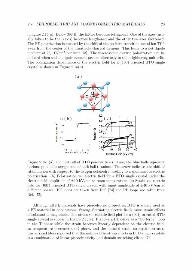
Barium titanate (BTO) is a typical FE material, which has received wide in-terest since the 1940s [71]. Single crystal BTO exhibits three distinct structuralphase transitions with decreasing temperature: cubic-to-tetragonal (C → T) at atemperature of T ≈ 393 K, tetragonal-to-orthorhombic (T → O) at T ≈ 278 Kand orthorhombic-to-rhombohedral (O → R) at T ≈ 190 K, respectively. C phaseis the paraelectric phase while the other three phases are ferroelectric phases. Thedetailed information about the lattice parameters at each phase can be seen in Fig-ure 2.14 [70].
Density functional theory calculations provide the interpretation of the ferroelec-tricity origin of BTO [72]. The barium ions occupy the corners of the cubic lattice,the oxygen ions the face centers and the titanium ions the body center, as displayed
2.7. FERROELECTRIC AND MAGNETOELECTRIC MATERIALS 23
in figure 2.15(a). Below 393 K, the lattice becomes tetragonal: One of the axes (usu-ally taken to be the c-axis) becomes lengthened and the other two axes shortened.The FE polarization is created by the shift of the positive transition metal ion Ti4+
away from the center of the negatively charged oxygens. This leads to a net dipolemoment of 26µ C/cm2 per unit [73]. The macroscopic electric polarization can beinduced when such a dipole moment occurs coherently in the neighboring unit cells.The polarization dependence of the electric field for a (100) oriented BTO singlecrystal is shown in Figure 2.15(b).
( a )
( b ) ( c )
Figure 2.15: (a) The unit cell of BTO perovskite structure; the blue balls representbarium, pink balls oxygen and a black ball titanium. The arrow indicates the shift oftitanium ion with respect to the oxygen octahedra, leading to a spontaneous electricpolarization. (b) Polarization vs. electric field for a BTO single crystal under theelectric field amplitude of ±10 kV/cm at room temperature. (c) Strain vs. electricfield for (001) oriented BTO single crystal with input amplitude of ±40 kV/cm atdifferent phases. FE loops are taken from Ref. [74] and PE loops are taken fromRef. [75].
Although all FE materials have piezoelectric properties, BTO is widely used asa PE material in applications. Strong alternating electric fields cause strain effectsof substantial magnitude. The strain vs. electric field plot for a (001)-oriented BTOsingle crystal is shown in Figure 2.15(c). It shows a PE curve as a ”butterfly” loopin the T phase while the strain becomes linearly dependent on the electric field,as temperature decreases to R phase, and the induced strain strength decreases.Caspari and Merz reported that the nature of the strain effects in BTO single crystalsis a combination of linear piezoelectricity and domain switching effects [76].

24 CHAPTER 2. THEORETICAL BACKGROUND
2.7.2 Magnetoelectric systems
Magnetoelectric (ME) materials are systems where the magnetization can be ma-nipulated by electric field or the polarization can be tuned by magnetic field. Thecoupling may arise directly between two order parameters or indirectly via strain.The magnetoelectric effect can be established in the form of electric polarization asa function of the magnetic field Pi(Hj) or magnetization as a function of the electricfield Mi(Ej).
Pi = αijHj +βijk2HjHK + · · · (2.30)
µ0Mi = αijEj +γijk2EjEK + · · · (2.31)
where E and H are the electric and magnetic fields, and α and β are the linear andnonlinear ME susceptibilities. The effect can be observed in both single phase MEmaterials and artificial ME heterostructures.
The single-phase ME materials can be classified into three different classes, de-pending on the microscopic mechanism of ferroelectricity, namely i) hybridizationeffects, such as BiFeO3. ii) Geometric constraints, such as YMnO3, and iii) electronicdegrees of freedom (spin, charge or orbital), such as TbMnO3 and LuFe2O4. TheMEC effect in single-phase ME materials is induced by intrinsic mechanisms [77, 78].
However, single-phase ME materials are very rare and their ME coefficients areusually too low to be used in applications. In order to overcome the shortages ofsingle-phase ME materials and provide new ME coupling (MEC) mechanisms, moreand more research interests have been moved to artificial ME materials in the lastdecades.
Remarkable MEC effects in artificial ME materials were reported [2, 79, 80]. TheMEC effect can be ascribed to the following two mechanisms: i) Direct coupling,MEC owing to an interfacial electronic effect. This type of mechanism has beentheoretically predicted based on bond-reconfigurations driven by ionic displacementor spin dependent screening mechanisms [4, 81, 82]. ii) Indirect coupling, MECmediated by strain. It means that the magnetization manipulation by the electricfield or the electric polarization manipulation by the magnetic field between thetwo phases is mediated via strain. This MEC effect has been evidenced in variousthin film systems [3, 6]. The MEC effect in artificial ME composites is induced byextrinsic mechanisms.
2.8 Scattering methods
Scattering is widely used as a non-destructive technique to study the structural andexcitation information in condensed matter physics. Depending on method, variousstructural information can be obtained. For instance, X-ray scattering is usuallyused as a method to provide the crystal structure while the magnetic structurecan be complemented using neutron scattering. The basic knowledge of general

2.8. SCATTERING METHODS 25
scattering and, especially, reflectometry theory is introduced in this section. For acomplete understanding of the scattering theory, please see Ref. [83].
2.8.1 Basics of scattering methods
In my thesis, only elastic scattering is considered. A schematic sketch of the elasticscattering experiment is displayed in Figure 2.16.
Figure 2.16: The sketch of a scattering experiment in the Fraunhofer approximation.Taken from Ref. [83].
The incident wave is produced by a monochromatic source and can be describedby a plane wave under the Fraunhofer approximation. The same applies for thescattered beam. The incident and scattered beam can be fully described by thewave vectors ~k and ~k′, respectively. For elastic scattering, k = |~k| = |~k′| = 2π
λ,
where λ is the wavelength of the neutron source. Hence, the so-called scatteringvector can be defined as
~Q = ~k′ − ~k (2.32)
with
| ~Q| = 4π
λsinθ (2.33)
In a scattering experiment, the intensity I( ~Q) is measured as a function of the
scattering vector ~Q. The scattered intensity is observed by the detector, whichcovers the solid angle dΩ = dS/r2 with the area dS of the detector and its distancer to the sample. The position of the detector is determined by the angles Θ and Φ, asdisplayed in Figure 2.17. The measured intensity from the detector is proportionalto the so-called scattering cross-section, which is corresponding to the probabilityfor an interaction of the incident beam with the sample. The sketch to define thescattering cross-section can be seen in Figure 2.17.
If N particles being scattered per second into a solid angle dΩ is seen by thedetector under a scattering angle 2θ, and the energy E is kept the same, then theso-called differential cross-section can be defined by
dσ
dΩ=
∫ ∞0
d2σ
dΩdEdE (2.34)

26 CHAPTER 2. THEORETICAL BACKGROUND
Figure 2.17: Geometry to derive the scattering cross-section. Taken from Ref. [83].
The differential scattering cross-section is proportional to the probability that aparticle is scattered into the solid angle dΩ by the interaction with the sample. Therelationship between the arrangement of the atoms in the sample and the scatteringcross-section dσ/dΩ is simplified using the so-called Born approximation, which isalso known as the kinematic scattering approximation.
In quantum mechanism, the probability to find a particle in the volume of d3ris given by the absolute square of the probability amplitude; hence, the differen-tial scattering cross-section, which is defined as the angular dependent scatteringprobability, can be expressed as |f( ~Q)|2, which reads as
(dσ
dΩ) = |f( ~Q)|2 =
m2
4π2~4
∣∣∣∣∫ V (~r′)ei~Q~r′d3~r′
∣∣∣∣2 (2.35)
where ~r is the sample to detector distance and V (~r) is the interaction potential ofneutrons.
2.8.2 Bragg scattering
X-rays and moderated neutrons are widely used to investigate the crystal structures,since the wavelengths of both beams are in the same range of the lattice distances.A plane wave with a wavelength λ scattered on an atomic periodical structure inconstructive interference yields Bragg reflections. The conditions for constructiveinterference are described by the so-called Bragg law:
n · λ = 2d · sinθ (2.36)
d is the interplanar spacing and θ is the scattering angle. The equivalence of theBragg law and the Laue condition stems from the relationship between real spaceand reciprocal space.
2.8.3 Grazing incidence scattering - Reflectometry
In reflectometry measurements, the scattering vector ~Q = ~k′ - ~k is close to 0, re-sulting in nearly no sensitivity to the atomic structures, which means no crystal-lographic Bragg scattering is visible. Instead, reflectometry measures the in-depth

2.8. SCATTERING METHODS 27
profile of the scattering potentials. Depending on different types of beams, nuclearor magnetic scattering length density (nSLD or mSLD) can be obtained. In thereflectometry setup, a monochromatic, collimated beam impinges upon the sampleunder a well-defined angle αi = θ (usually 5o). Most of the beam scattered atthe sample is reflected by the sample within a so-called specular scattering. Theincoming angle αi and outgoing angle αf are always kept the same, leading to the
scattering vector ~Q being always perpendicular to the sample surface. The beams arereflected from different interfaces, so that constructive and destructive interferenceof beams reflected from the two interfaces are displayed as peaks, the so-called Kies-sig fringes. The layer thickness information is included in the peaks. Furthermore,lateral correlations can be probed in the so-called off-specular or diffuse scatteringat angles αi 6= αf .
In contrast to the diffraction experiment, the Born approximation is no longervalid for reflectometry measurements, because multiple scattering in the reflectionmode cannot be neglected [84]. Since the Q region covered by reflectivity measure-ments is not sensitive to the atomic periodical structure, it is possible to describe thescattering potential within the continuum approximation. ~Q is always perpendicularto the surface; the scattering potential of the sample can be simplified only in the zcomponent V (z). In the thickness direction, the beam is partly transmitted to thesubstrate and partly reflected. The reflection (transmission) coefficients is definedas the modulus squared of the ratio of the amplitudes of reflected (transmitted) andincoming waves. They are represented by R and T and expressed by the Fresnelequations:
R =
∣∣∣∣θ − nθtθ + nθt
∣∣∣∣2 (2.37)
T =
∣∣∣∣ 2θ
θ + nθt
∣∣∣∣2 (2.38)
θt is the transmission angle of the beam, n = 1 − δ + iβ is the index of refraction,shown in Figure 2.18. Depending on the different types of materials and beams, thevalues of the scattering power δ and absorption β will be determined.
For most materials, the refractive index n is smaller than 1, which leads to atotal reflection in the sample. The total reflection means that during the reflectom-
t
Figure 2.18: Typical geometry of reflectometry under the grazing incident angle θ.

28 CHAPTER 2. THEORETICAL BACKGROUND
etry process, when the incident angle is smaller than the critical angle θc, all thebeam are reflected and no beam transmitted into the sample. Hence, the intensitydependence of Q shows a plateau during the total reflection process. When theincident angle above the θC , the intensity drops as |Q|4, assuming a perfect smoothsurface without further layer structures. Roughness will additionally speed up theintensity decrease, which can be described by the Debye-Waller model, multiplyingI(Q) ∼ eQ
2zσ
2with the roughness σ of the surface. For a multilayer system, e.g. a
thin film on a substrate, an iterative formalism, describing the scattering processusing the reflection and transmission coefficients in each material, is introduced inRef.[85].
Polarized neutron reflectometry (PNR)
For magnetic materials, the unpaired electrons inside the atoms will show a magneticmoment and will additionally generate a magnetic induction field ~B. Fortunately,the neutron is a particle with 1/2 spin; by using neutrons as the beam, one can probethe magnetic structure of the matter, besides the nuclear structure. The interactionpotential for neutrons can be averaged from the Fermi-pseudo-potential to:
V (Z) =2π~2
mN
ρNb− γnµN~σ · ~B (2.39)
The first item is the nuclear potential, while the second one is the magnetic potential.mN is the mass of neutron, ρN is the nuclear density and b is the scattering length.~σ = (σx, σy, σz) is the vector of Pauli-matrices. The gyromagnetic factor γn =−1.913 and the nuclear magneton µN = 5 · 10−27 J/T are two constant coefficients.With this interaction potential, the differential magnetic scattering cross-section canbe described as
dσ
dΩ= (γnre)
2 1
2µB|〈σ′z|~σ · ~M⊥( ~Q)|σz〉|2 (2.40)
where re is the radius of electron and σz is the spin projection along a quantizationaxis given by the external field. ~M⊥ = Q× ~M × Q is the Fourier transformation ofthe magnetization component of the sample, which is perpendicular to the scatteringvector ~Q. The equation tells us that only the in-plane magnetization component,which is perpendicular to the ~Q, can be measured. The typical geometry of a PNRexperiment at the sample position is shown in Figure 2.20. The magnetic induction~B0 = µ0
~H is constant over the sample and gives a constant contribution to the indexof refraction.
Hence, this contribution cancels out for the calculation of refraction and trans-mission. Depending on the neutron beam polarization before and after the sample,one can define four channels, namely R++, R−−, R+− and R−+. The former twoare called non-spin-flip channels and the neutron spin direction is not changed afterit is scattered at the sample, while the later two are called spin-flip channels. Thepolarized neutron beam can be described by plane waves with two spin componentsψ+(~r) and ψ−(~r), for polarization ”up” and ”down”. The Schrodinger equations for

2.8. SCATTERING METHODS 29
BII
B
?
B
Hext
n , n ,
Figure 2.19: The geometry of PNR experiment at the sample position. Neutronsare polarized, either parallel or antiparallel to the external magnetic field Hext. Themagnetic signal in samples are induced by the external magnetic field, leading to amagnetic induction of B = µ0(Hext +M)), while ~B|| and ~B⊥ are two projections of~B with respect to Hext.
the potential of neutron state can be simplified as coupled equation as
ψ′′+(z) + [k2z − 4πbρN +
2mγnµn~2
B||]ψ+(z) +2mγnµn
~2B⊥ψ−(z) = 0 (2.41)
ψ′′−(z) + [k2z − 4πbρN −
2mγnµn~2
B||]ψ−(z) +2mγnµn
~2B⊥ψ+(z) = 0 (2.42)
In the R++ channel, the contribution of the potential comes from the magneticscattering added with nuclear scattering, while they are subtracted in the R−−channel. The contribution from the spin flip channel is the magnetization of the B⊥component.
Reflectivity data reduction
Figure 2.20: PNR simulation of the sample (substrate) BTO/(7 nm) Ti/(22 nm)Fe2O3/(25 nm) Au by GenX, the R++ and R−− channels are simulated togetherwith the reference value of every parameter of every component layer.

30 CHAPTER 2. THEORETICAL BACKGROUND
The XRR and PNR data are analyzed by fitting the reflectivity curve using theParratt formalism [85] within the framework of the program ”GenX” [86]. Thefitting result yields a structural model for the investigated sample.
In XRR reflexivity, a structural model is used for the sample, which usually con-sists of the ambient environment, the substrate and the layers. Several parametersare used to describe the substrate and layers, for example, the stoichiometry of thematerial, the layer thickness, roughness and nSLD. The simulated X-ray reflexiv-ity of the sample can be implemented by the structural parameters. The fittingprocedure will give the best representation of the raw data, by modifying the openparameters. For PNR measurements, a magnetic profile needs to be added besidesthe structural model, which is mainly represented by mSLD. In PNR simulation,the R++ and R−− channels are simulated at the same time by the combination ofthe nuclear and magnetic scattering length density (SLD).
In our simulation, different models are used for finding the best fitting of ourmeasured results, which are illustrated in Chapter 4. For evaluating the goodness ofthe fit, the Figure of Merit (FOM) is used to calculate the average of the absolutedifference between the logarithms of the data YQ and the fitting SQ:
FOMlog =1
N − 1·∑Q
|lgYQ − lgSQ| (2.43)

Chapter 3
Methods and Instruments
In this chapter, the instruments and methods for the sample preparation and inves-tigation used in the thesis are briefly introduced. Also, the colloidal self-assemblymethods are described.
3.1 NP self-assembly methods
The NP preparation and assembly methods can be divided into two groups de-pending on the growth strategy [87, 88]. To the first group belong the top-downmethods. Materials start from large structure sizes and end up with small struc-tures via several methods. These methods include deposition techniques, such assputtering evaporation and laser ablation.
The other group consists of bottom-up methods. Nanostructure units are stackedon each other onto the substrate and self-organized into desired structures and func-tionalities via interaction forces. For example, NP building blocks can be used tobuild monolayer or multilayer structures by some degree of control to direct the ag-gregation process. These methods comprise self-organization of nanostructures andself-organization of nanostructures on templates. Comparing with the top-downmethod, bottom-up methods are easier to access and much cheaper. They can alsoproduce homogenous nanostructures with few defects and long-range order, if theaggregation process is properly controlled.
( b ) ( c )( a )
Substrate
Substrate Substrate
Substrate
Figure 3.1: Schematics of NPs self-assembly routes: (a) Sedimentation, (b) Drop-casting and (c) Spin coating
Colloidal self-assembly methods of nanostructures are the most simplest methods
31

32 CHAPTER 3. METHODS AND INSTRUMENTS
to prepare homogenous 2D and 3D NP arrangements. In this thesis, three self-assembly methods have been used, as shown in Figure 3.1. The parameters of eachmethod are optimized to obtain NP arrangements with the best long-range orderand least defects.
The first self-assembly method is sedimentation. Here, the NP dispersion sed-iment onto the substrate driven by gravity. The NP self-assembly process occursduring the evaporation of the solvent.
The second is dropcasting. The NP suspension is pipetted onto the substratedirectly and the NPs self-assemble on the substrate during the evaporation.
The third method is spin coating. The substrate is fixed onto a rotating stageof a spin coating device via a vacuum pump. The NP suspension is dropped ontothe substrate and subsequently spin coated with a tunable rotation speed and time.The thickness of the NP layer can be controlled by adjusting the rotation speed,time and the concentration of the NP suspension. Optimized parameters for a 2DNP monolayer are searched and recorded in the section 4.1.2.
3.2 Scanning Electron Microscopy (SEM)
The morphology of nanoparticles and thin films has been probed using a Scan-ning Electron Microscope (SEM, SU8000, Hitachi) at the institute PGI-7. In SEM,a beam of electrons is generated by a field emission gun. The electron beam isaccelerated through high voltage and passes through a system of apertures and elec-tromagnetic lenses to produce a focused beam of electrons. The beam scans thesurface of the specimen by means of scan coils. Secondary electrons are emittedfrom the specimen and collected by a detector [89].
Two most commonly used modes in SEM are the secondary electron (SE) modeand the backscattered electron (BSE) mode. The SE mode is the process of detectionof secondary electrons emitted by atoms in the specimen excited by the primaryelectron beam via inelastic scattering. By scanning the specimen and collecting thesecondary electrons using a detector, an image that displays the morphology of thesample can be obtained. This mode is widely used to capture surfaces and providehigh-resolution images. The BSE mode is the process of collecting the scatteredprimary beam electrons, scattered from the sample. BSEs emerge from deeperlocations within the specimen and can probe the distribution of different elementsin the sample. In our thesis, the SE mode has been used to check the morphology ofthe as-prepared thin film and NP arrangement, while the BSE mode has been usedto analyse the layer structure of the ME sample.
3.3 Scanning Transmission Electron Microscopy
(STEM)
The stacking geometry and the element distribution of the sample in cross-sectionaldirection are measured using a Scanning Transmission Electron Microscope (STEM,

3.4. ATOMIC FORCE MICROSCOPY (AFM) 33
FEI Titan 80-200) at the Ernst Ruska-Centre (ER-C) at the ForschungszentrumJulich.
STEM is a type of transmission electron microscope (TEM). However, a STEMoperates in a very similar way to a SEM; a focused electron beam is scanned overthe sample. Electrons which pass through the sample are collected to produce avariety of transmission images.
The rastering of the beam across the sample makes STEM suitable for analyticaltechniques, such as High Angle Annular Dark-Field imaging (HAADF). The imagesarise from elastically scattered electrons. The HAADF signal is directly proportionalto the density and thickness of the specimen and proportional to Z3/2, where Z isthe atomic number. Thus, it is possible to obtain images which show the contrastdue to the mass-thickness or Z contrast.
STEM also offers microanalysis capabilities, i.e. energy dispersive X-ray analysis(EDX) and electron energy loss spectroscopy (EELS). In conventional TEM, thespatial resolution is limited to tens of A, by the interaction volume of the beamwithin the sample. However, in STEM, the EDX analysis can be performed at thenanometer scale. EELS offers elemental mapping at 2 nm spatial resolution andachieves real-time mapping, which is particularly useful for the determination ofvalencies of the light elements and transition metals.
3.4 Atomic Force Microscopy (AFM)
The topography of the sample was probed by an Atomic Force Microscope (AFM,Agilent Technologies 5400).
Hereby, three types of modes are relevant, according to the nature of the tipmotion: contact mode, tapping mode and non-contact mode. In our work, the non-contact mode is the most frequently used mode. Here, the tip is close enough todetect the sample surface for short-range forces (distance < 10 nm). Moreover, thetip avoids touching the sample surface.
In the probing process, the cantilever is first excited close to its resonant fre-quency. After the tip is brought in proximity of the sample surface, forces betweenthe tip and the sample lead to a deflection of the cantilever, according to Hooke’slaw. The deflection changes its amplitude due to the various interactions betweenthe surface and the tip. The deflection amplitude as the recorded signal reflects theheight profile of the sample surface (Figure 3.2).
The topographic image, amplitude image, phase image and deflection image arerecorded simultaneously in one measurement. Topography is often the most relevantone. It is possible to estimate both the lateral (xy) and height (z) information fromthis image; hence, the surface quality can be probed in terms of surface roughness.The root mean square roughness (Rq), which indicates the height distribution of thesurface, is also an often-used parameter.

34 CHAPTER 3. METHODS AND INSTRUMENTS
Scanner
A B
C D
( a ) ( b )
Figure 3.2: (a) Block diagram of AFM using beam deflection detection. As thecantilever is displaced via its interaction with the sample surface, the reflection ofthe laser beam is displaced on the surface of the photodiode; furthermore, the heightand phase information are also calculated and obtained. (b) The AFM imagingmodes: contact mode and tapping or non-contact mode.
3.5 Piezoresponse Force Microscopy (PFM)
The piezoresponse of BTO substrates with the application of a voltage was probedusing a Piezoresponse Force Microscope (PFM, Keysight 9500 AFM) at the institutePGI-6.
PFM measures the mechanical response when an electrical voltage is applied tothe sample surface using a conductive tip. In response to the electrical stimulus, thesample locally expands or contracts, as shown in Figure 3.3.
A B
C D
A B
C D
A B
C D
Figure 3.3: Depiction of the PFM operation. The sample deforms in response to theapplied voltage, which, in turn, causes the cantilever to deflect. This can then beinterpreted in terms of the piezoelectric properties of the sample. Image courtesy:S. Jesse, ORNL.
When the tip is in contact with the surface, the local piezoelectric response isdetected as the first harmonic component of the tip deflection. The phase ϕ of theelectromechanical response of the surface yields information about the polarizationdirection below the tip.
For c− domains (polarization vector oriented normal to the surface and pointing

3.6. SQUID MAGNETOMETRY 35
downward), the application of a positive tip bias voltage results in the expansion ofthe sample. The surface topography is in phase with the tip voltage, i.e. ϕ = 0.
For c+ domains, the response is opposite and ϕ = 180. The detection of lateralcomponents of the polarization can be realized by lateral PFM, which is a techniquewhere the in-plane component is detected as lateral motion of the cantilever due tothe bias-induced surface shearing. This option was not available at the instrumentused here, unfortunately.
3.6 SQUID magnetometry
The Magnetic Property Measurement System (MPMS, Quantum Design) is a ded-icated equipment used for measuring the magnetic properties of various types ofsamples. Here, an external magnetic field up to 7 T with a field uniformity of 0.01%over a range of 4 cm can be applied. The MPMS also provides a high-precisiontemperature unit that covers a temperature range of 1.9 to 400 K.
The MPMS magnetometer utilizes a Superconducting Quantum Interference De-vice (SQUID) to probe the magnetization very precisely down to 10−11 A · m2. TheSQUID magnetometer has as its main element a superconducting ring incorporatedwith a Josephson junction; the junction is inductively coupled to a RF circuit.
The sample moves through the second-derivative coils resulting in an inductivecurrent. The current causes a magnetic field at the SQUID and leads to a impedancechange in the superconductor ring and subsequently causes a change of the voltageamplitude in RF circuit. The change in the voltage amplitude gives the responsefunction with respect to the sample position. Hence, the magnetic moment of thesample can be determined by fitting the measured response curve to a theoreticalone.
The Reciprocating Sample Option (RSO) is a sample transport mode for sampleswith small magnetic moment. RSO offers a relatively fast type of measurement,which then allows averaging and good noise rejection. Another frequently usedoption is the DC option, which is also the default mode in MPMS. Here, a steppedDC scan is performed and the sample starts at the lowest point of the scan lengthand sequentially moves the sample upwards through the pickup coils.
More details regarding the SQUID magnetometry can be found in the MPMShardware manual [90].
Since the manipulation of the magnetization with respect to an applied electricfield is of interest, not only magnetic fields, but also electric fields need to be appliedto the sample. One can apply electric fields throughout the sample via conductivewires from a power supply. The sample is fixed at a Vespel rod which is covered bya straw. The Vespel rod is further connected to a conductive sample rod. Electricconnection between the sample and the power supply is implemented by two copperwires and the sample rod. One wire is attached on the surface of the sample viasliver paste and the other wire to the bottom. Both voltages at the positions ofsample and the power source were measured to make sure the voltage loss on theway from power source to sample is less than 5%.
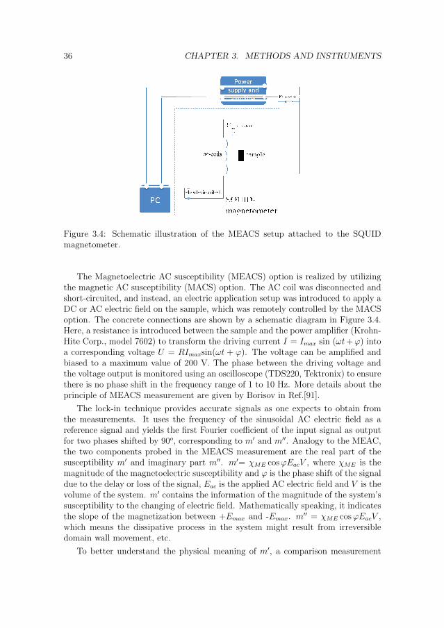
36 CHAPTER 3. METHODS AND INSTRUMENTS
Figure 3.4: Schematic illustration of the MEACS setup attached to the SQUIDmagnetometer.
The Magnetoelectric AC susceptibility (MEACS) option is realized by utilizingthe magnetic AC susceptibility (MACS) option. The AC coil was disconnected andshort-circuited, and instead, an electric application setup was introduced to apply aDC or AC electric field on the sample, which was remotely controlled by the MACSoption. The concrete connections are shown by a schematic diagram in Figure 3.4.Here, a resistance is introduced between the sample and the power amplifier (Krohn-Hite Corp., model 7602) to transform the driving current I = Imax sin (ωt+ϕ) intoa corresponding voltage U = RImaxsin(ωt + ϕ). The voltage can be amplified andbiased to a maximum value of 200 V. The phase between the driving voltage andthe voltage output is monitored using an oscilloscope (TDS220, Tektronix) to ensurethere is no phase shift in the frequency range of 1 to 10 Hz. More details about theprinciple of MEACS measurement are given by Borisov in Ref.[91].
The lock-in technique provides accurate signals as one expects to obtain fromthe measurements. It uses the frequency of the sinusoidal AC electric field as areference signal and yields the first Fourier coefficient of the input signal as outputfor two phases shifted by 90o, corresponding to m′ and m′′. Analogy to the MEAC,the two components probed in the MEACS measurement are the real part of thesusceptibility m′ and imaginary part m′′. m′= χME cosϕEacV , where χME is themagnitude of the magnetoelectric susceptibility and ϕ is the phase shift of the signaldue to the delay or loss of the signal, Eac is the applied AC electric field and V is thevolume of the system. m′ contains the information of the magnitude of the system’ssusceptibility to the changing of electric field. Mathematically speaking, it indicatesthe slope of the magnetization between +Emax and -Emax. m
′′ = χME cosϕEacV ,which means the dissipative process in the system might result from irreversibledomain wall movement, etc.
To better understand the physical meaning of m′, a comparison measurement

3.6. SQUID MAGNETOMETRY 37
between m′ and ∆M in dependence of temperature on the system of Au / BTO/ Ti / NP / Au was probed and shown in Figure 3.5. In the ∆M measurement,electric fields were manually tuned between +Emax and -Emax at each temperaturepoint, and at each +Emax and -Emax, the m+E or m−E was measured, respectively.∆M was obtained by the subtraction of m+E and m−E. As seen from the figure,∆M follows the behavior of the temperature dependent m′ measured in the MEACSoption, i.e. the signal jump happens at both phase transitions, which is indicatedas the grey bars in the figures, and the scales of both measurements also match.Thus, the result reveals that if the AC electric field amplitude and frequency werecontrolled in a reasonable low range, m′ approximately equals the magnetizationdifference between +Emax and -Emax.
( a )
( b )
Figure 3.5: m′ and ∆M in dependence of temperature on sampleAu/BTO/Ti/Ti/NP/Au (a) MEC measured with MEACS option in MPMS at thefrequency of 1 Hz and Emax of 3.2 kV/cm. (b) measured in the DC option in MPMSwith an attached electric power source to apply 3.2 kV/cm on the sample, ∆M isobtained by manually switching the electric field polarization point by point andsubtracting each negative to positive electric field result.
However, to be comparable with other ME materials, m′ is converted into theso-called real part of the ME coefficient αME = µ0m′
EV= µ0M ′
E, where µ0 is the vacuum
permeability. m′′ is conversed into the imaginary part of the ME coefficient αME =µ0M ′′
Ein the following results. The specific derivation of real and imaginary parts of
αME to be µ0M′/E and µ0M
′′/E and their units are attached in appendix A.
A reference sample, a Cr2O3 single crystal (3 mm x 3.5 mm x 0.5 mm), was usedto calibrate the MEACS setup. The measured results were compared to the resultsmeasured in W. Kleemann’s group as shown in Figure 3.6. The ME coefficientαME is introduced from the equation αME = µ0m′
EV, where m′ is the measured real
part of the susceptibility, E is the applied electric field and V is the volume of themeasured sample. From the figure, one finds that the reference data corresponds

38 CHAPTER 3. METHODS AND INSTRUMENTS
Figure 3.6: ME coefficient αME of a Cr2O3 single crystal vs temperature measuredat f = 1 Hz and Emax = 63.4 kV/m after ME field cooling. Reference data pointsare reproduced from W. Kleemann (see Ref [91]). The y = 0 line is a regular line ofthe coordinate system.
with the literature data.
3.7 X-ray Reflectometry/Diffractometry (XRR, XRD)
The thickness, roughness and crystalline quality of the prepared layers, includingthin films and self-assembled NP layers, were characterized using the X-ray diffrac-tometer (D8 Advanced, Bruker AXS) at JCNS-2.
An X-ray beam with a wavelength of λ = 1.54 A is generated by a Cu-κα sourceand collimated by a Gobel mirror and two slits. A monochromator is used to narrowdown the wavelength band of the X-ray source. A vacuum sample stage is availableto provide the possibility of measuring the sample in vacuum. Moreover, a tem-perature unit can be attached to the sample stage to measure the sample in thetemperature range from room temperature to 700 K. A heater and a water coolingsystem are responsible for warming up and cooling down, while a thermocouple isused to measure the temperature. Besides this, a knife-edge collimator is installed tohave an optimal collimation of the incident beam and a suppression of background.The outgoing beam passes another combination of Gobel mirror and slits and isrecorded by the detector.
The X-ray diffractometer mode is used to determine the crystalline quality andout-of-plane lattice parameters. It also can be used in a reflectometer mode toinvestigate the thickness and laterally averaged roughness of the film. To fulfill therequirements of each kind of experiment, the slits can be changed.

3.8. GRAZING INCIDENCE SMALL ANGLE X-RAY SCATTERING (GISAXS)39
3.8 Grazing Incidence Small Angle X-ray Scatter-
ing (GISAXS)
The size distribution of NPs as well as the in-plane correlations of self-assembled NPswere determined using the grazing-incidence small-angle X-ray scattering (GISAXS)instrument GALAXI at JCNS-2.
The X-rays are produced by an electron beam hitting a liquid metal jet of aGaInSn alloy. After the parabolic optics, the X-ray beam is directed through the4 m long collimation. Afterwards, two slits are used to define the size of the beam.The beam arrives at the sample position with a flux of 1·109 photons/mm2·s.
The sample can be adjusted in the beam with 2 translational and 2 rotationaldegrees of freedom. After the X-ray beam is scattered at the sample, the reflectedbeam is received by a detector with 169 x 179 mm2 active area. The distance betweenthe sample position and the detector can be adjusted from 835 mm to 3535 mm to fillthe material with different correlation sizes up to 200 nm. The schematic diagram ofthe GISAXS geometry on a self-assembled NP monolayer can be seen in Figure 3.7.
Figure 3.7: The geometry for GISAXS experiments. The Bragg reflections aresuperimposed by the blurry powder rings. This results from the scattering of theX-ray on the carbon gratings, which are in front of the 2D detector in order to fixthe Kapton window.
The intensity of the X-ray beam detected by the 2D detector provides informationabout the electron density profile of the NPs statistically averaged over the area ofthe illustrated sample. With ~Q being the scattering vector, lateral correlationsare found in the Qy direction, while out-of-plane correlations are probed in the Qz
direction. The 2D detector hereby records the Qy - Qz plane. For the case of amonolayer of NPs, and hence, for the case of a 2D lattice, Bragg peaks appear asvertical stripes in the Qy - Qz detector plane. Their intensity along Qz in modulateddue to the laterally averaged electron density distribution in the layer.

40 CHAPTER 3. METHODS AND INSTRUMENTS
The stripe distance d and the lattice constant a are related according to theequation
dhk =a√
4(h2+hk+k2)3
=2π
Qhky
(3.1)
Here, h and k are the Miller indices and Qhky is the position of the rods (2D-Bragg
peak).
3.9 Polarized neutron reflectometry (PNR)
The magnetization depth profile of the iron oxide NP monolayers were investigatedusing Polarized Neutron Reflectometry (PNR) at the instrument MARIA at HeinzMaier-Leibnitz Zentrum (MLZ) in Munchen.
Figure 3.8: Schematic setup of the Polarized neutron reflectometer MARIA.
The setup is schematically shown in Figure 3.8. The white neutron beam isproduced by the reactor and passes through a velocity selector. Since MARIA isdesigned for a Q range from (0.002 A−1 to 3.2 A−1 ), the velocity selector choosesthe wavelength from 4.5 A to 40 A and provides a wavelength distribution of 4λ/λ= 0.1. Next to the velocity selector is a polarizer. The beam is polarized by adouble reflection polarizer, which is essential for the PNR. A RF-flipper is used toflip the spin state of neutrons. Before the neutron beam is scattered by the sample,a pair of slits is used to optimize the beam size to balance the resolution and thefinal intensity.
The setup is optimized for sample sizes of 1 x 1 cm2 by using a vertical focusingelliptic neutron guide. The sample is mounted on a hexapod, which provides themovement of the sample. The sample space is covered by the closed cycle cryostatthat can be pumped to 10−6 mbar, which reduces the scattering from are during themeasurement. Meanwhile, the cryostat provides the temperature, ranging from 4 Kto room temperature. This space is the only region in the entire measurement pathwhere one can manipulate the magnetic field. A special sample holder is designedfor our measurements to apply an electric field on the sample. The sample holderis made of aluminum and covered with boron, which is a good neutron absorber.

3.9. POLARIZED NEUTRON REFLECTOMETRY (PNR) 41
The bottom electrode is connected to the ground of the cryostat via the aluminumholder, while the top electrode is connected by a copper wire to the electric generatorthrough the pinhole in the cryostat. With this setup, a voltage of up to 500 V canbe applied at the sample position.
Behind the sample, the neutron state is analyzed via a 3He cell analyzer fora full horizontal polarization analysis. Finally, the neutrons are detected using a400 x 400 mm2 3He 2D detector..
200 400 800600200
400
600
800
(3)(1)
(2)
ypix
el/
x pixel/
I/co
unts
Figure 3.9: Detector image taken at MARIA. (1) is the tail of the almost blockeddirect beam and the intensity in the rest area, (2) represents the region of interest,which is the beam reflected region, and (3) contributes to the background.
The instrument saves one detector image for each angle, and an example of thedetector image is shown in Figure 3.9. The almost blocked tail of the direct beamis shown in region (1). The reflected beam is shown in region (2), which is also theregion of interest. A Gaussian profile is used to fit the distribution to give the finalintensity. Region (3) indicates the background that comes from the scattering onair, the sample holder and the other components within the neutron beam path.For every final reflected intensity, the background intensity has to be subtracted.At last, the final reflected intensities are collected to obtain the final Q-dependentreflectivity curve.

42 CHAPTER 3. METHODS AND INSTRUMENTS

Chapter 4
Results I: Iron oxide NPs on BTOsingle crystals
In this chapter the results of the iron oxide NPs on BTO substrates are presented.Iron oxide NPs are self-assembled on BTO substrates as monolayers and multilayers,respectively. First, the results on the characterization of the structural propertiesof BTO substrates are presented. This is followed by the magnetic and magneto-electric properties of the sample iron oxide NP monolayers on BTO substrates asthe main part. After the analysis of the magnetic profile performed by PNR, thecharacterization and investigation results of the iron oxide NP multilayers on BTOsubstrate are introduced.
4.1 Sample preparation
The characterization of the BTO substrates will be presented including their topog-raphy, piezoelectric property, dielectric property and domain deformation dependingon electric field and temperature. Afterwards, the preparation of the samples rang-ing from BTO / NP monolayers up to the final sample Au / BTO / Ti / NPmonolayers / Au will be introduced.
4.1.1 BTO single crystals
(001) oriented BTO single crystals with the size of 5 mm × 5 mm × 0.5 mmand 5 mm × 5 mm × 0.1 mm are commercially available from CrysTech GmbH.These BTO single crystals are used as substrates to support the self-assembledNP monolayers. Since clean substrates are needed to obtain smooth films, the BTOsubstrates were first cleaned with acetone to remove organic residuals on the surface.Afterwards, they were annealed at 1200 K in an oxygen atmosphere at a pressureof 1 ·10−6 mbar for 6 h to remove adatoms like carbon. The surface quality waschecked by AFM and the surface topography is shown in Figure 4.1(a). A stripe-like corrugation is seen from the figure. The possible reason responsible for the
43

44CHAPTER 4. RESULTS I: IRON OXIDE NPS ON BTO SINGLE CRYSTALS
( a )( b )
Figure 4.1: (a)Topography of the (001) oriented BTO substrate measured by AFM.The stripe pattern in the image results from the different domain structures in theBTO substrate. (b)Line scan profile. The position of the extracted line is indicatedas a black line in (a), the line cut profile indicates BTO corrugations reaching aheight of up to 8 nm.
corrugations is the formation of differently oriented a- and c- domains in the BTOin the tetragonal phase at room temperature.
In order to quantitatively evaluate the roughness of the substrate, a line cutperpendicular to the long direction of domain structures was made which is markedas a black line in the AFM image. The plot in Figure 4.1(b) indicates that eachdomain structure has a width around 0.2 µm. It is clearly seen that some domaincorrugations reach a height of 8 nm. They are the main cause of the surface rough-ness.
The piezoelectric response of the BTO substrate was evaluated by PFM at thePGI-6, Forschungszentrum Julich which is shown in Figure 4.2. The [001] direction
( a )( b )
( d )
( c )
( e ) ( f )
Figure 4.2: BTO substrate measured by PFM.(a) and (d) represent the electrodepattern. The white area is the area where the voltage of +3V was applied andthe black area is where -3V was applied. (b) and (e) are the PFM phase imagesmeasured during the electric field application. (c) and (f) are the PFM phase imagesmeasured after removing the electric field.

4.1. SAMPLE PREPARATION 45
of the as-prepared BTO substrate was aligned parallel to the sample stage. Thesample was measured in the range of 10 × 10 µm2. For the PFM measurement, apatterned electrode was attached to the sample to provide the electric field. Theschematic drawing of the electrode pattern is shown in Figure 4.2 (a) and (d). Theinner square has a size of 5 × 5 µm2. During the measurement of (b), +3 V wereapplied to the white area and -3 V were applied to the black area. After poling for30 s, the phase image of the BTO substrate was recorded as shown in (b). The innersquare shows a polarized phase of 60 degrees while the outer shell shows a polarizedphase of -60 degrees.
The application of a higher voltage is not possible in this setup. It can beexpected that one could polarize the two areas by a 180 degree difference with alarger voltage [92]. The same measurement was conducted again immediately afterremoving the electric field. The BTO substrate shows a remanent polarization.However, the remanent polarization vanishes with time. The electrode pattern onthe BTO substrate with an opposite electric field was applied and similar resultsare seen in (e) and (f). PFM measurements thus reveal the polarization state of theBTO surface and that it can be tuned under electric fields of few volts.
Figure 4.3: Permittivity versus temperature of the 0.5 mm thick BTO substrate.An AC electric field was applied to the sample Au/BTO/Au. The sample was firstcooled down from 300 K to 10 K without electric field and by the application of anAC electric field, the sample was probed while warming up and subsequent coolingdown.
The temperature dependent permittivity of the BTO substrates was investigatedusing the Closed Cycle Measurement System (CCMS) from Cryogenics Ltd. Hereby,a sample with 10 nm Au / 0.5 mm BTO / 10 nm Au was prepared. The results areshown in Figure 4.3. The sample was first cooled down to 10 K. Afterwards, an ACelectric field with a frequency of 9 Hz and amplitude of 20 kV/cm was applied to thesample. The measurements were carried out first during the direction of warmingup (FW) and then cooling down (FC).
Two peaks are observed in both curves, 197 K and 289 K for the FW branchand 183 K and 279 K for the FC branch, respectively. The first peak at lowertemperature indicates a phase transition from the R to O phase, while the other
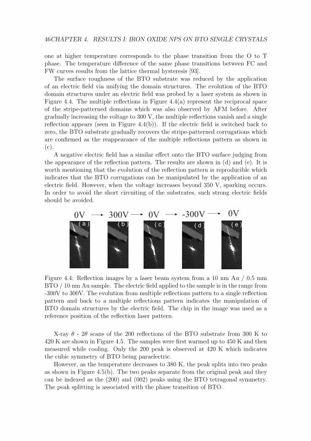
46CHAPTER 4. RESULTS I: IRON OXIDE NPS ON BTO SINGLE CRYSTALS
one at higher temperature corresponds to the phase transition from the O to Tphase. The temperature difference of the same phase transitions between FC andFW curves results from the lattice thermal hysteresis [93].
The surface roughness of the BTO substrate was reduced by the applicationof an electric field via unifying the domain structures. The evolution of the BTOdomain structures under an electric field was probed by a laser system as shown inFigure 4.4. The multiple reflections in Figure 4.4(a) represent the reciprocal spaceof the stripe-patterned domains which was also observed by AFM before. Aftergradually increasing the voltage to 300 V, the multiple reflections vanish and a singlereflection appears (seen in Figure 4.4(b)). If the electric field is switched back tozero, the BTO substrate gradually recovers the stripe-patterned corrugations whichare confirmed as the reappearance of the multiple reflections pattern as shown in(c).
A negative electric field has a similar effect onto the BTO surface judging fromthe appearance of the reflection pattern. The results are shown in (d) and (e). It isworth mentioning that the evolution of the reflection pattern is reproducible whichindicates that the BTO corrugations can be manipulated by the application of anelectric field. However, when the voltage increases beyond 350 V, sparking occurs.In order to avoid the short circuiting of the substrates, such strong electric fieldsshould be avoided.
0V 300V 0V -300V 0V( a ) ( b ) ( c ) ( d ) ( e )
Figure 4.4: Reflection images by a laser beam system from a 10 nm Au / 0.5 mmBTO / 10 nm Au sample. The electric field applied to the sample is in the range from-300V to 300V. The evolution from multiple reflections pattern to a single reflectionpattern and back to a multiple reflections pattern indicates the manipulation ofBTO domain structures by the electric field. The chip in the image was used as areference position of the reflection laser pattern.
X-ray θ - 2θ scans of the 200 reflections of the BTO substrate from 300 K to420 K are shown in Figure 4.5. The samples were first warmed up to 450 K and thenmeasured while cooling. Only the 200 peak is observed at 420 K which indicatesthe cubic symmetry of BTO being paraelectric.
However, as the temperature decreases to 380 K, the peak splits into two peaksas shown in Figure 4.5(b). The two peaks separate from the original peak and theycan be indexed as the (200) and (002) peaks using the BTO tetragonal symmetry.The peak splitting is associated with the phase transition of BTO.

4.1. SAMPLE PREPARATION 47
( a )
( b )
( c )
Figure 4.5: Temperature dependent XRD scans on the 200 Bragg peak of the BTOsubstrate. The samples were first heated up to 450 K and measured while coolingdown in the sequence of (c) 420 K (b) 380 K (a) 300 K. The black line is used for abetter visualization of the peak shift. The Cubic and Tetragonal phases are markedunder the consideration of theoretical values.
Depending on the direction of the lattice extension, a-type and c-type domainsare formed [68]. However, the narrow peaks indicate that BTO at this temperatureshows a coexistence of C and T phases with the cubic lattice still dominating. Thepeak splitting becomes more pronounced after further decreasing the temperatureto 300 K which suggests that more a- and c-type domains are formed. Due tolimitations of our setup, it is not possible to measure the domain state below roomtemperature.
4.1.2 NPs self-assembled on BTO
Iron oxide spherical shaped NPs with a diameter of 20 nm and 8% size distributionwere commercially obtained from Ocean NanoTech LLC (See Appendix B). TheNPs were synthesized by thermolysis of an iron precursor in presence of oleic acidand dispersed in toluene. The initial composition is a mixture of ferrimagneticmaghemite (γ-Fe2O3) and antiferromagnetic wuestite(FexO) [94, 95].
In order to obtain homogenous 2D iron oxide NP monolayers on BTO substrates,three different colloidal self-assembly methods were used to self-assemble iron oxideNPs. The schematics of the three methods are depicted in Figure 3.1. The firstmethod is sedimentation and is shown in Figure 3.1(a). BTO substrates were placedat the bottom of a beaker which is filled with toluene. 30 µl of iron oxide NPssolution was dropped into the beaker by a transferpettor. The gravity driven NPsedimentation took 1 h. Afterwards, the solution was evaporated in air for 12 h and

48CHAPTER 4. RESULTS I: IRON OXIDE NPS ON BTO SINGLE CRYSTALS
500 nm
100 nm
200 nm
( b )
200 nm
( a )
( c ) ( d )
Figure 4.6: SEM images of iron oxide NPs self-assembled on a BTO substrate usingthe three methods, (a) sedimentation (b) dropcasting (c) spin coating at 50 rps for45 s (d) spin coating at 15 rps for 20 s. The inset in (b) is a zoom-in look of thearea indicated by the arrow.
NPs self-assembled on top of the BTO substrate during this period. The results areshown in Figure 4.6(a). The particles are arranged in a disordered state and someparticles are aggregated in 3d clusters. Hence it departs from our aim to prepare ahomogenous NP monolayer.
The second method is dropcasting. The schematic is shown in Figure 3.1(b). Inthe dropcasting process, 5 µl NPs solution are taken and dropped onto a 5 × 5 mm2
sized BTO substrate. The solvent evaporated in air and the NPs self-assembledduring this period. NPs mesocrystals were formed by this route and the resultsare shown in Figure 4.6(b). The cracks between mesocrystals developed at themoment when the sample is nearly dry. The NP arrangement is better seen fromthe zoomed-in image as shown in the inset. The NPs are arranged in an hexagonalpattern. However, the surface is still not homogenous enough.
The third method is spin-coating whose schematic diagram is shown in Fig-ure 3.1(c). The optimized parameters for preparing a 2D NP monolayer were de-termined after the iteration of preparation and characterization. First, the NPssolution was diluted by a factor of 10 with toluene solvent. Then 2.5 µl dilutedNPs solution were dropped onto a 5 × 5 mm2 BTO substrate. After spin coating at50 rps for 45 s, a homogenous NP monolayer was prepared. The results are displayedin the Figure 4.6(c). The NPs self-assembled into a hexagonally closed-packed ar-rangement as a monolayer of particles with approximately 80% coverage averagedover the substrate. For fabrication of NP multilayers, 15 rps and 20 s were usedduring the spin coating process while the other parameters were kept the same. The

4.1. SAMPLE PREPARATION 49
morphography of multilayers is seen in Figure 4.6(d). The surface of the layer ishomogenous and in some regions, NPs are arranged almost in a crystalline fashion.
( b )( a )
Figure 4.7: (a) Magnetic moment versus temperature curves of a NP monolayer ontop of a BTO substrate after ZFC and FC measured at a magnetic field of 5 mTby SQUID.(b) Magnetic moment versus magnetic field at 300 K and 5 K for thesame sample. The inset shows the schematic of the sample and the direction of themagnetic field applied on it.
The magnetization of the NP monolayers on BTO substrates as a function oftemperature or magnetic field is shown in Figure 4.7. The M-T curve displayed inFigure 4.7(a) shows a typical superparamagnetic behavior of iron oxide NPs, i.e. theFC and ZFC curves show a peak marking the blocking temperature of the iron oxideNPs at around 275 K. The M-H curves of the sample, displayed in Figure 4.7(b)were probed at 300 K and subsequently at 5 K. The closed hysteresis loop at 300 Kindicates the unblocked state of superparamagnetic NPs while the open loop at 5 Kcorresponds to the blocked state.
The exchange bias effect observed from the hysteresis loop at 5 K is due to theexistence of the AFM component FeOx (wustite) inside the NPs. FeOx has a Neeltemperature of 190 K [94].
4.1.3 BTO / Ti / NP monolayers
For the samples of the type BTO / Ti / NP monolayer, before the NPs were spin-coated onto the BTO substrate, a Ti buffer layer of 7.8 nm thickness was depositedonto the BTO using a molecular beam epitaxy (MBE) setup (please see Section5.3.1). The surface quality of the film was checked by the XRR and the data ispresented in the next section.
In order to remove the organic oleic acid shell around the NPs, the sampleswere treated in an oxygen plasma asher (PNA Telpla 300, CNST) with an oxygenpressure of 0.3 mbar, a gas flow of 200 ml/min and a power of 3000 W for 5 min.After oxygen plasma etching, a fraction of γ-Fe2O3 is hereby transformed into Fe3O4.The influence of oxygen plasma etching onto iron oxide nanoparticles is similar to thethermal annealing process as reported both by M. J. Benitez and Gena Wilbs [94, 95].

50CHAPTER 4. RESULTS I: IRON OXIDE NPS ON BTO SINGLE CRYSTALS
4.1.4 Au / BTO / Ti / NP monolayer / Au
In order to obtain more pronounced ME coupling effect, a 25 nm thick Au cappinglayer was deposited again by MBE. For electrical contacting and to apply an electricfield across the sample, a second Au layer was deposited onto the opposite BTO sur-face. In this way the two Au layers serve as bottom and top electrode, respectively.Moreover, several reference samples, i.e. without Ti layer, without NPs, without Aucapping or using a Si substrate instead of BTO have been prepared to compare tothe complete sample (Au / BTO / Ti / NPs / Au).
In order to check the thickness and roughness of the as-prepared samples, XRRwas used to measure the samples in each preparation step and the results are col-lected in Figure 4.8.
( b ) ( c )
( a )
Figure 4.8: (a) XRR measurements for each sample preparation step from BTOsubstrates to the final sample BTO / Ti / NP / Au. The arrow indicates thepreparation sequences of each sample with the sample geometry marked besides it.The fit of the XRR data of the samples BTO / Ti and BTO / Ti / NP are given assolid lines. The resulting SLD as a function of the layer thickness for (b) the sampleBTO / Ti and (c) the sample BTO / Ti / NP.
The XRR curve of BTO substrates shows a plateau and then dies out veryquickly indicating a large roughness of the surface.
The XRR curve of BTO / Ti shows several Kiessig oscillations up to a Q valueof 0.6 A−1 indicating a good quality of the Ti film. The further results of the fitshows the thickness of the Ti layer is 7.8 ± 0.3 nm and the roughness is 0.3 nm.The nSLD is plotted against the layer thickness z in Figure 4.8(b). The real part ofnSLD gives the dispersion while the imaginary part gives the absorption.

4.2. RESULTS 51
The XRR curve of BTO / Ti / NP shows an additional superimposed peak atthe first two oscillations which corresponds to the NP monolayer. The results fromthe fit provides a NP monolayer thickness of 22.4 ± 1.1 nm with a roughness of3.1 nm. The nSLD as a function of z is plotted in Figure 4.8(c).
The XRR curve of BTO / Ti / NP /Au shows only two broad Kiessig oscillationswhich is due to the large SLD and absorption of Au layer to the X-ray. X-rays onlypenetrates several nanometers into the Au layer and are blind to the layer below.
4.2 Results
At the beginning of this section, the morphology of the self-assembled NPs on BTOsubstrates are presented being characterized by SEM and GISAXS. Further mea-surements were performed on BTO / Ti / NP / Au samples by SEM and STEM.The magnetic properties were studied using a SQUID magnetometer, the MEC ef-fect using a MEACS option attached to the SQUID magnetometer and the E fieldmanipulation of the magnetic depth profile using PNR.
4.2.1 Macroscopic magnetic properties
Q [nm ]y
-1
Q[n
m]
z
-1
( d )
( b )( a )
Q [nm ]y
-1
(10)
(11)(20)
107
106
105
104
103
102
101
-1.00 -0.75 -0.50 -0.25 -0.00 0.25 0.50 0.75
Q [nm ]y
-1
ExperimentFit
( c )
Figure 4.9: (a) GISAXS pattern of an iron oxide NP monolayer spin-coated onto aBTO substrate (sample BTO / NP). The white line is a dead region of the detector.(b) Simulation of the GISAXS data by the BornAgain software. (c) shows theintensity of experimental (black dash line) and simulated (red solid line) data as afunction of Qy with the integration of Qz (d) shows a line cut of raw data along Qy
at Qz = 0.5 nm−1 along with a Gaussian fit (red line) to the (10) Bragg peak. Braggpeaks were indexed according to a hexagonal lattice with a = 21 nm.

52CHAPTER 4. RESULTS I: IRON OXIDE NPS ON BTO SINGLE CRYSTALS
A 8 nm thick Ti buffer layer on top of BTO substrate is prepared using an MBEsetup before the NPs were spin-coated onto the BTO substrate. Subsequently, NPswere self-assembled onto the BTO / Ti layer by spin coating, as described in section4.1.2. During the spin-coating procedure, the NPs self-assemble in a hexagonallyclosed-packed arrangement as a monolayer of particles with approximately 80% cov-erage averaged over the substrate. The overall morphologies of the self-assembledNPs was studied by GISAXS which are shown in Figure 4.9(a). The angle of theincident beam is αi = 0.1. The observed vertical intensity rods in the Qz directionare due to the monolayer nature of the NPs. The 2d-Bragg rods were successfullyindexed assuming a two-dimensional closed packed hexagonal lattice with a latticeconstant of a = 21.03 ± 0.53 nm. The observed stripe positions and calculatedpositions based on the NP diameter match well confirming the hexagonal arrange-ment. The data is fitted by the BornAgain software as shown in Figure 4.9(b). Atruncated spherical NP shape is found to give a better fitting of the data, whichmight be due to the fact that X-rays with a certain incident angle only see a part ofthe spheres. The experimental data and its fitting are shown in Figure 4.9(c), thefitting intensity as a function of Qy with the integration of Qz shows a good agree-ment with the experimental data. The fitting confirms a hexagonal closed packedNP arrangement and the 21 nm lattice constant. The line cut at Qz = 0.5 nm−1
along Qy is shown in Figure 4.9(d). The intensity modulation along Qz is relatedto the laterally averaged electron density of the NP layer. The plot demonstratesthat the rods are relatively sharp in Qy direction, indicating a good lateral order.After taking the instrument resolution into account, a Lorentzian profile is used tofit to the first order peak which yields a structural coherence length of 168 ± 9 nm,which indicates a relatively good supercrystalline NP ordering.
The NPs are coated with organic oleic acid shell, in order to remove the shellto get a more direct and pronounced MEC effect, the sample was treated in anoxygen plasma asher (PNA Telpla 300, CNST) for 5 mins with an oxygen pressureof 0.3 mbar, a gas flow of 200 ml/min and a power of 3000 W. Structural charac-terization of the NP ordering of the sample is performed using SEM as displayedin Figure 4.10(a) for the uncoated sample. From the comparison between the SEMpictures of NPs before and after oxygen plasma, it can be seen that the oxygenplasma treatment has obviously no effect on the ordering of the NPs.
Figure 4.10(b) and (c) show the results of different sample processing steps, i.e.after oxygen plasma etching to remove the oleic acid shells (Figure 4.10(b)) withthe 8 nm Ti layer between the substrate and NPs, and after coating the NPs witha 25 nm Au layer (Figure 4.10(c)). The Au coating almost covers perfectly theNP layer as a percolated Au network embedding the NPs. This is evidenced by ourSTEM/EDX observation.
Figure 4.11(a) shows the morphology of the multilayer system viewed along thecross-sectional direction. The upper white area represents hereby the Au layer. Theelemental maps (Figure 4.11(b–f)) detected by EDX clearly identify the Au / NP,NP / Ti and Ti / BTO interfaces, in which the BTO / Ti and Ti / NP interfaces arefurther manifested by the dark-contrast stripes in the oxygen map. It can be clearly

4.2. RESULTS 53
( b ) ( c )( a )
Figure 4.10: (a) Zoomed-in on-top view of the BTO / NP sample observed by SEM.(b) A similar sample but with an 8 nm Ti layer deposited before spincoating theNPs. Moreover, the sample was treated in oxygen plasma (sample BTO/Ti/NP).(c) The same sample after deposition of a 25 nm Au capping layer on top of the NPs(sample BTO / Ti / NP / Au). Note the different scale between (c) and (a)(b).
BaTiFe Au O10 nm( a ) ( d )( b ) ( c ) ( e ) ( f )
Figure 4.11: Energy-dispersive X-ray spectroscopy in scanning transmission electronmicroscopy mode (STEM–EDS) acquired at 200 kV.(a–f) Z-Contrast high-angleannular-dark-field STEM image showing the stacking sequence of different layers inthe BTO / Ti / NP / Au sample and the simultaneously collected EDX maps ofFe (blue), Au (pink), O (yellow), Ti (green) and Ba (red), respectively. The scalebar in (a) represents 10 nm vertically. The scales are identical for the panels (a–f).The dashed circles with a radius of 21 nm in (d) indicate the NPs as a guide to theeye.
seen that the top surface of the Ti layer is oxidized while the bottom surface isoxygen-free, i.e. the dark band at the Ti / BTO interface indicating a pure metallicTi layer. In addition, the coverage of the Au layer of about half of the particlediameter is revealed from the Fe and Au maps, see Figure 4.11(b and c). Theoxygen map in Figure 4.11(d) shows that there is no oxygen gap between the TiO2
layer and NPs. This is most probably due to the fact that the NPs are attachedwith the TiO2 layer after oxygen plasma treatment.
A more direct evidence of the oxidized Ti layer can be seen in electron energy lossspectroscopy (EELS) of Ti which is displayed in Figure 4.12. The EELS experimentswere performed on an FEI Titan 80-200 Chemi-STEM microscope with an operatingvoltage of 200 kV. The energy resolution for the EELS experiments was 1.5 eV,which is defined by full-width-at-half-maximum of the zero-loss peak. The energydispersion used for collection of the electron energy loss spectrum is 0.25 eV/pixelwith an entrance aperture of 2.5 mm.
The high-angle annular dark-field image (HAADF) is shown in Figure 4.12(a)where the lattice planes of the BTO substrate can be seen. The EELS of the elements

54CHAPTER 4. RESULTS I: IRON OXIDE NPS ON BTO SINGLE CRYSTALS
Figure 4.12: EELS study of sample Au / BTO / Ti / NPs / Au. (a) high-angleannular dark-field image (HAADF) image of the cross-sectional nanostructure. Theyellow dashed line denotes the linear region of interest for EELS characterization.(b)-(d) Stacked absorption edges of (b) Ti-L2,3,(c) Fe-L2,3 and (d) Ba-M4,5 collectedfrom the linear region of interest indicated in (a). The vertical axis corresponds tothe real space distance in (a).
Ti, Fe and Ba are shown in (b) to (d) respectively. The two vertical stripes in thebottom part of the Ti map indicates the uniform valency state of Ti in the BTOsubstrate. The two brighter oblique stripes above represent the different Ti valencystates in the Ti and TiO2 layer. The Fe map indicates the uniformity of the Fevalence state of iron oxide NPs. However, the broadness of the stripes indicate thecoexistence of several iron valences states.
Moreover, several reference samples, i.e. without Ti layer, without NPs, withoutAu capping or using a Si substrate instead of BTO have been prepared to compareto the complete sample (Au / BTO / Ti / NPs / Au).
Magnetometry measurements were performed using a superconducting quantuminterference device (SQUID) magnetometer.
On these three sample structures magnetometry measurements were performed.Figure 4.13 (a-c) shows the magnetic moment as function of temperature for (a)the untreated NP monolayer on top of the BTO substrate (BTO/NP), (b) the oxy-gen plasma treated NP monolayer deposited onto a Ti buffered BTO substrate(BTO/Ti/NP), and (c) the complete system, where the NPs are embedded in anAu top layer (BTO/Ti/NP/Au).
In each case the measurement protocol was the following: starting from 300 Kthe samples were first cooled in zero field down to 10 K. Subsequently, a constantfield of 5mT was applied and the field warming (FW) curve recorded upon warmingup to 350 K. At the same applied field the sample was then cooled and the FC curverecorded. All three measurements were performed at the same cooling/heating rateof 2 K/min. In Figure 4.13, the FC and FW curves are displayed to show possibletemperature hysteresis effects upon warming vs. cooling. The results shown inFigure 4.13(a-c) were taken with magnetic fields oriented in-plane.
The comparison of the data from the three systems yields several interestingobservations. For the sample BTO/NP, the FC and FW curves are basically identicalto each other and only a slight kink at the R−O phase transition at 190 K can beseen (Figure 4.13(a)). Since the particles are only weakly bound to the substrate

4.2. RESULTS 55
Figure 4.13: (a-c) In-plane magnetic moment vs. temperature during field warming(FW) and during subsequent field cooling (FC) in 5 mT for the three types ofsamples, (a) BTO / NP, (b) BTO / Ti / NP and (c) BTO / Ti / NP / Au asdepicted schematically in the insets. (d) Out-of-plane magnetic moment underthe same conditions to be compared to (c). The vertical grey bars indicate thetemperature region, where bulk BTO has first order phase transitions from the Tto O to R phase. TV indicates the Verwey transition of magnetite.

56CHAPTER 4. RESULTS I: IRON OXIDE NPS ON BTO SINGLE CRYSTALS
by van der Waals interactions and because they are coated with an organic shell,no MEC is expected here. We attribute this kink to the magnetic response of thedipolarly coupled NPs to a change of the BTO corrugation and hence to the slightpositional rearrangement of the NPs. Apart from the kink the curves are identicalto those obtained on NPs on a Silicon substrate [24].
Self-assembled iron oxide nanoparticles on BTO substrates show typical super-paramagnetic behavior (ZFC and FC curves of sample BTO/NP can be seen inFigure 4.7(a)). They correspond to the response of dipolarly interacting iron oxideNP [94].
For the sample BTO/Ti/NP, the FC and FW curves show magnetization stepsnear the R−O transition at 190 K and the O−T transition at 287K (Figure 4.13(b)).We assume that strain mediated MEC is responsible for the observed magnetiza-tion changes. The oxygen plasma treatment burnt the oleic acid surrounding theNPs into a carbon shell. In addition, the surface of the Ti layer was oxidized intotitanium oxide. The carbon shell and the oxidized titanium oxide appear to be thecritical components for providing a good adhesion of NPs to the BTO substrate, giv-ing rise to a non-vanishing MEC. Comparable samples without a Ti layer yield nomagnetization steps which confirms the observation made in Ref. [23]. We assumethat strain-mediated coupling is dominant, because any significant charge effect willplay no role due to the conductive Ti layer and the carbonized NP shells.
One should note that the kink found at ca. 110 K after oxygen plasma etchingis due to a fraction of maghemite / wustite is transformed into magnetite. Hereby,the influence of oxygen plasma etching onto iron oxide nanoparticles is similar tothe thermal annealing as reported by M. J. Benitez et al. [94].
The results on the BTO / Ti / NP / Au sample display also magnetization jumpsbut with a significantly enhanced amplitude as shown in Figure 4.13(c). Our inter-pretation is that the embedding Au layer effectively mediates the strain producedby the BTO substrate onto the NPs and hence increases the MEC between BTOand NPs.
Second, one should note the sign of the magnetization changes and the relativeamplitudes at the phase transition temperatures. Here we focus on the completesystem BTO / Ti / NP / Au. With increasing temperature, at the O −→ R transitionat around 190 K, a positive magnetization step is found for the FC curve and anegative for the FW curve. The FC curve hereby displays an about three timeslarger jump compared to the FW curve. Due to the first order nature of the BTOphase transitions these features exhibit a temperature hysteresis. At the T −→ Otransition at around 280 K the FC curve shows a negative magnetization step, whilethe FW is basically unaffected.
In order to investigate the MEC effect at the high temperature transition ofBTO (C to T phase) onto the magnetism of the NPs, the PPMS VSM Oven optionwas employed. The sample BTO / Ti / NP / Au was measured from 300 K to450 K in the sequence of FW and subsequently FC and the results are displayed inFigure 4.14(a).
It can be seen that a magnetization jump is formed in FW and FC curves at

4.2. RESULTS 57
( a )
( b )
Figure 4.14: (a) In-plane magnetic moment vs. temperature during FW and duringsubsequent FC in 5mT for the sample BTO / Ti / NP /Au as depicted schemat-ically in the insets (b) In-plane FC under different magnetic fields for the sampleBTO / Ti / NP / Au.

58CHAPTER 4. RESULTS I: IRON OXIDE NPS ON BTO SINGLE CRYSTALS
around 400 K which corresponds to the BTO phase transition from C to T. Moreover,a thermal hysteresis behavior between FW and FC is observed and the gap of thehysteresis is reduced to 5 K, which is coincident with the thermal hysteresis behaviorof the BTO lattice change, which can be seen in Figure 2.14.
In order to obtain a better insight into the origin of the MEC between iron oxideNPs and BTO substrate, we also investigated the magnetic field dependence of themagnetization jumps. The results are shown in Figure 4.14(b). It can be seen thatthe magnitude of the magnetization jumps are suppressed by the increased magneticfield and vanish under a magnetic field of 0.5 T.
To check for an anisotropy effect, we performed an analogous measurement withthe magnetic field oriented perpendicular to the sample plane. The results obtainedon the identical sample as in Figure 4.13(c) are shown in Figure 4.13(d). One findsan overall much smaller amplitude of the magnetization jumps. In addition, thesigns of the magnetization steps are reversed.
To understand the observed effects one should note that the magnetoelasticenergy gives rise to an uniaxial anisotropy which can be expressed as ∆E = (-3/2)λ∆σsin2θ [16, 96], where λ is the effective magnetostriction coefficient of theNPs, σ is the induced effective strain and θ is the angle between the measuredmagnetic moment and the σ-axis.
It can be deduced that if the compressive or tensile strain is abruptly increased,θ will tend to be 90 or 180 in order to minimize the anisotropy energy. Further-more, the magnetization projection onto the in-plane and out-of-plane direction willincrease or decrease causing an increase or decrease of the magnetization, corre-spondingly.
Taking the O −→ R phase transition for an example, the a(b) axis lattice param-eter changes abruptly from 4.012 A to 3.998 A leading to an in-plane contraction ofεab = 1
2(εxx + εyy)= 0.18%, where εxx and εyy are the xx and yy components of the
strain tensor of BTO. The in-plane compressive stress transmits via the interface ofthe Ti/TiO2 layer and the Au matrix onto the NPs. This causes the increase in mag-netization of the in-plane component via changing the direction of magnetizationeasy axis. The relation between strain and magnetism becomes more complex atthe O−T transition, because the twinning domain state occurring at this transitionresults in an randomly distributed and hence in total smaller strain [70, 93].
The strain anisotropy energy effect was further investigated by the tempera-ture dependence of the ratio of the remanent magnetization (Mr) to the saturationmagnetization (Ms) and coercivity (Hc).
The magnetic hardness, Mr / Ms, (sometimes also referred as ”squareness” ofthe hysteresis loop) is a quantitative measure of magnetic anisotropy, but also of themagnetization reversal mode (i.e. domain wall motion vs. coherent or incoherentrotation) [97]. Here we can assume that the reversal mode inside the NPs will stayunchanged, i.e. the reversal will always occur via rotation of the superspins of theNPs [24]. Therefore the hardness value will yield information on changes of theanisotropy.
Figure 4.15(a) displays four examples of hysteresis loops for the sample BTO/Ti/NP/Au

4.2. RESULTS 59
Figure 4.15: (a) In-plane zoomed-in hysteresis loops of the sampleBTO / Ti / NP / Au above and below the O − R phase transition mea-sured in cooling direction. (b-d) Values of magnetic hardness Mr / Ms (blackcircles) and coercivity Hc (red squares) vs. temperature obtained from in-planehysteresis loops (b-c) on the sample BTO/NP (b) and BTO/Ti/NP/Au (c). Panel(d) shows the corresponding out-of-plane data for the sample BTO/Ti/NP/Au.The dashed line marks the Neel temperature of bulk FeO.

60CHAPTER 4. RESULTS I: IRON OXIDE NPS ON BTO SINGLE CRYSTALS
above and below the R−O phase transition measured in cooling direction with in-plane geometry. From such loops we extracted both the hardness and the coercivityHc, as function of temperature (Figure 4.15(b-d)).
The MEC effect at the R − O phase transition at about 185 K can be clearlyseen in Figure 4.15(c) as a peak in both the hardness and the coercive field. Thesample and the measurement geometry (in-plane field) are hereby the same as forFigure 4.13(c). The increase in the hardness means that the MEC to the BTOinduces an additional magnetic anisotropy in the NPs. The comparison to the resultswith the perpendicular geometry shows that the induced anisotropy direction liespreferentially in-plane as only a slight jump is observed in the perpendicular case atthis temperature.
One should note that also other effects might give rise to a temperature de-pendent change of the anisotropy. One is the exchange bias (EB) effect [98]. OurNPs are composed of ferrimagnetic maghemite and magnetite and antiferromagneticwustite and it was previously shown that comparable particles exhibit an EB effectbelow the Neel temperature of wustite [94]. Therefore we have performed analo-gous measurements on the reference system BTO/NPs. The results are shown inFigure 4.15(b). One finds that below about 198K the hardness and coercivity in-creases with decreasing temperature as expected for an EB effect, but no peak isobserved. Therefore we conclude that the peak in Figure 4.15(c) is due to MECcoupling between NPs and BTO.
Besides the anisotropy change induced by temperature, an anisotropy changecaused by an electric field can be found. Magnetic hysteresis loops with simultaneousapplication of electric field of E = 0 kV/cm and ± 3.6 kV/cm were performed usingthe regular MPMS DC option with a special sample holder. Measurements of theM-H curves were performed at 300 K and 5 K, respectively.
The data is shown in Figure 4.16. The hysteresis loops at different electric fieldsat 300 K are shown in Figure 4.16(a). A typical superparamagnetic behavior isobserved. No modification of the magnetization with respect to the applied electricfield is observed. Both Mr and Hc keep the same value for the conditions of E =0 kV/cm, +3.6 kV/cm and -3.6 kV/cm. The hysteresis loops at different electricfields at 5 K are shown in Figure 4.16(b). Both Mr and Hc change dramaticallyafter the electric field application. The application of the electric field leads to aincrease of the coercivity of 26.3 %. The hardness is increased from 0.47 to 0.88.
The magnetic moment as function of the applied DC electric field at room tem-perature can be seen in Figure 4.17. In order to maximally saturate the BTOsubstrate, a 0.1 mm thick BTO substrate is used in this measurement. Other sam-ples are prepared on 0.5 mm thick BTO substrates. As seen from the figure, atypical butterfly shaped curve was obtained as expected from in-plane strain medi-ated MEC in ME composites [99]. This indicates that the magnetization of the ironoxide NPs follows the strain varied during the electric field application.
MEACS was measured on the same SQUID magnetometer with an additionalupgrade implemented as described in section 3.6.
So far, the observed effects are due to structural phase transitions of the BTO
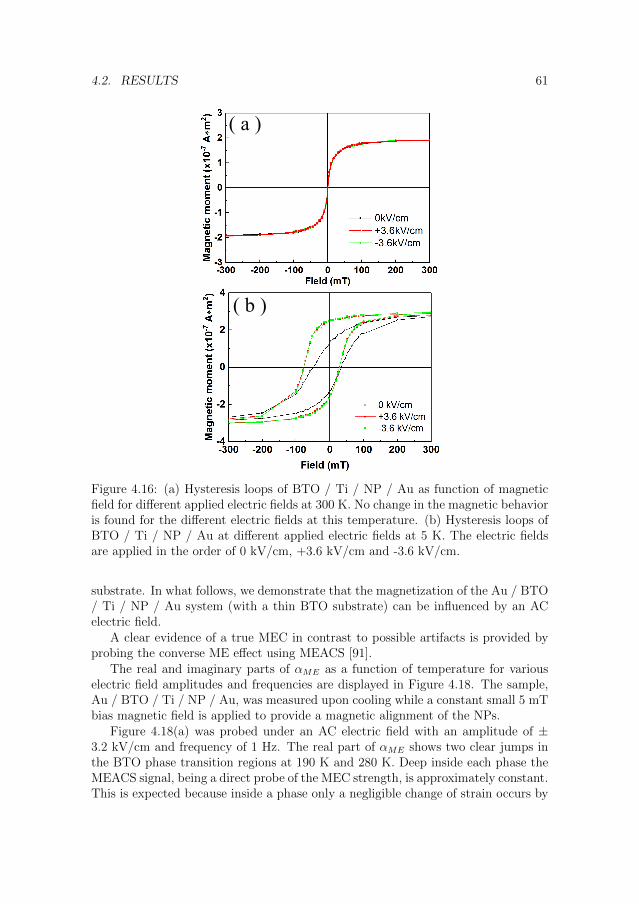
4.2. RESULTS 61
( a )
( b )
Figure 4.16: (a) Hysteresis loops of BTO / Ti / NP / Au as function of magneticfield for different applied electric fields at 300 K. No change in the magnetic behavioris found for the different electric fields at this temperature. (b) Hysteresis loops ofBTO / Ti / NP / Au at different applied electric fields at 5 K. The electric fieldsare applied in the order of 0 kV/cm, +3.6 kV/cm and -3.6 kV/cm.
substrate. In what follows, we demonstrate that the magnetization of the Au / BTO/ Ti / NP / Au system (with a thin BTO substrate) can be influenced by an ACelectric field.
A clear evidence of a true MEC in contrast to possible artifacts is provided byprobing the converse ME effect using MEACS [91].
The real and imaginary parts of αME as a function of temperature for variouselectric field amplitudes and frequencies are displayed in Figure 4.18. The sample,Au / BTO / Ti / NP / Au, was measured upon cooling while a constant small 5 mTbias magnetic field is applied to provide a magnetic alignment of the NPs.
Figure 4.18(a) was probed under an AC electric field with an amplitude of ±3.2 kV/cm and frequency of 1 Hz. The real part of αME shows two clear jumps inthe BTO phase transition regions at 190 K and 280 K. Deep inside each phase theMEACS signal, being a direct probe of the MEC strength, is approximately constant.This is expected because inside a phase only a negligible change of strain occurs by

62CHAPTER 4. RESULTS I: IRON OXIDE NPS ON BTO SINGLE CRYSTALS
Figure 4.17: Magnetic moment vs. applied electric field of sampleAu / BTO / Ti / NP / Au at 300 K and 5 mT. The black square points weremeasured with increasing DC field from -20 to +20 kV/cm while the red circleswere measured in reversed sequence.
lattice expansion only. However, near the BTO phase transitions a large change ofthe MEC and hence a jump in the MEACS signal is observed due to the step-liketransformation of the BTO lattice parameters, the change in the domain structureand consequently the change in the BTO surface morphology. The imaginary partof αME is constantly zero in the measured temperature range because under suchlow frequency, there is nearly no delay between the incoming and outgoing signaland almost zero dissipation through the sample.
The same sample was measured with an increased frequency of 9 Hz while otherparameters were kept constant (Figure 4.18(b)). Both MEACS coefficients becomemore noisy and the two steps in the real part of αME become less obvious. Onepossible explanation is that while the lock-in technique only allows the signal of theselected frequency to be received, the strain generated by the BTO phase transitionshas a frequency dependence that does not follow the electric field.
Under the larger frequency of 9 Hz, the imaginary part of αME starts to deviatefrom zero and the deviation become larger when the frequency is increased to 19 Hzwhich is shown in Figure 4.18(c). In principle, the imaginary part of αME indi-cates the delay and dissipation in the sample. The increasing nonzero value of theimaginary coefficient indicates an increasing dissipation as the frequency increases.
A smaller electric field strength causes a smaller amplitude of the steps in realpart of αME and a smaller nonzero value in imaginary part of αME. This is foundwhen the electric field strength decreased to 1.8 kV/cm and the frequency decreasedto 1 Hz and 9 Hz (Figure 4.18(d) and (e)).
To systematically investigate the effect of frequency and amplitude of the ACE-field onto the real part of αME, the frequency and amplitude dependency of thereal part of αME is measured which is shown in Figure 4.18(f) and (g), respectively.

4.2. RESULTS 63
Figure 4.18: The real and imaginary parts αME vs temperature measured in a AC E-field with different frequencies f and E-field amplitude Emax and a constant magneticfield of 5 mT, (a) at Emax=3.2 kV/cm and f=1 Hz, (b) at Emax=3.2 kV/cm andf=9 Hz, (c) Emax=3.2 kV/cm and f=19 Hz, (d) Emax=1.8 kV/cm and f=1 Hz,(e) Emax=1.8 kV/cm and f=9 Hz, (f) the real part αME as a function of frequencymeasured at 300 K and Emax=3.2 kV/cm, (g) the real part αME as a function ofE-field strength measured at 300 K and 1 Hz. The two black lines at 192 K and280 K in figure (a) to (e) indicate the R-O and O-T phase transitions of the BTOsubstrate. The measuring geometry is shown as the inset in (a). Both real andimaginary part αME are shown in the same scale for better comparison.
Both curves were measured from zero to maximum value first, and then decreasedback. At low frequency, the real part of αME is almost frequency independent andvery close to zero. The real part of αME decreases to negative values above 300 Hz(Figure 4.18(f)). In the electric field amplitude dependence seen in Figure 4.18(g),the ∆M is the absolute value of the difference between the coefficients obtained at

64CHAPTER 4. RESULTS I: IRON OXIDE NPS ON BTO SINGLE CRYSTALS
each positive and negative electric field. As expected, the coefficient increases asthe electric field frequency or strength increases.
Moreover, we have measured two reference samples, i.e. one with a bare BTOsubstrate contacted with a bottom and top electrode (sample Au/BTO/Au), andone with only a silicon substrate with NPs (sample Au / Si / NP / Au). Bothsamples show only white noise without any specific features (see Figure 4.19). Theresults rule out any MEACS signal from the BTO substrate and from the NPs alone,respectively.
( a ) ( b )
Figure 4.19: ME coefficient of (a) Au / BTO / Au and (b) Au / Si / iron oxideNPs / Au systems in dependence of temperature measured at f = 1 Hz and Emax= 4 kV/cm after ME field cooling. The samples stacking are displayed as thediagrammatic drawing inside each figure.
We also measured, with the same protocol, but with a larger saturating constantmagnetic field of 100 mT, and found no jump. This is in accordance with the factthat a larger Zeeman energy stabilizes the NP magnetization along the field directionwhich results in a smaller influence of the ME effect.
The real and imaginary parts αME as function of magnetic field are shown inFigure 4.20. The measurements were taken at 300 K, 270 K and 180 K whichcorresponds to the T, O and R phases of BTO, respectively. The measurementstarted from zero magnetic field and then was increased to +0.5 T, reduced to -0.5 Tand finally swept back to zero. Both parts of αME only show a field dependence inthe region between 150 mT and -150 mT. The data beyond that region is not shownin order to clearly show the region of interest.
The measurement at 300 K shows a hysteresis behavior of the real part of αME
(Figure 4.20(a)). The maximum and minimum values of the coefficient occur at+7 mT and -7 mT, respectively. The coefficient decreased to zero when the magneticfield increased beyond these fields. The imaginary part of αME is zero within theentire magnetic field range.
Figure 4.20(b) shows the αME at 270 K, which is corresponding to the O-phaseof BTO. A less obvious hysteresis behavior of the real part of αME between 50 mTand -50 mT is observed, while the maximum and minimum coefficient happen at+8 mT and -8 mT. Moreover, one should note that the amplitude of the real partof αME is smaller than that in the T-phase indicating a temperature dependent real

4.2. RESULTS 65
( a )
T
( b )
O
( d )
OR
( c )
300K 270K
180K
180K
300K 270K
270K
270K
Figure 4.20: The real part and imaginary part of αME vs. magnetic field measured inan AC E field with amplitude Emax= 3.2 kV/cm, frequency f=9 Hz and a constantmagnetic field of 5 mT, (a)at 300 K (b) at 270 K (c)at 180 K (d)at 270 K with anAC electric field of Emax=3.2 kV/cm and f=199 Hz, The phases of BTO in everymeasurement are marked. The schematic of the sample used in this measurementis represented as the inset in (a).
part of αME. The imaginary part of αME still stays constantly zero.After decreasing the temperature to 180 K, corresponding to the R-phase of BTO,
the real part of αME shows an nearly unobservable hysteresis and no maximum andminimum values can be found (Figure 4.20(c)). The imaginary part of αME remainszero,which means the imaginary part of αME is temperature independent.
An AC electric field with a larger frequency of 199 HZ was applied to the sampleto investigate the frequency dependence of both parts of αME. In order to simplifythe figure, only measurements in the O-phase are shown while measurements in theother two phases show similar results. As the frequency increases, the amplitudeof the real part of αME increases and the maximum and minimum values shift to± 20 mT respectively (Figure 4.20(d)). The imaginary part αME shows a sizeablevalue of 40 ns/m. It is due to the effect of strain mediated magnetism of iron oxideNPs via magnetostriction.
The αME is expressed as [100],
αME ∝ q1d1Eac (4.1)
where q1 is the effective magnetostrictive coefficient of the iron oxide NPs, d1 is the

66CHAPTER 4. RESULTS I: IRON OXIDE NPS ON BTO SINGLE CRYSTALS
piezoelectric coefficient of the BTO substrate and Eac is the applied AC E field. q1
can be expressed as
q1 = δλ/δH (4.2)
where λ is the magnetostrictive strain and H is the applied magnetic field. Thehysteresis response of the real part of αME can be interpreted by the magnetostric-tive coefficient curve of iron oxide. For instance, the magnetostriction of an ironoxide single crystal shows an increase tendency with a diminishingly accelerationuntil it becomes flat after the saturation magnetic field of 30 mT is reached [100].Mathematically, the S-shaped αME vs. H results from the first derivative of themagnetostriction curve of iron oxide and the maximum and minimum values of realpart are related to the largest magnetostrictive coefficient of iron oxide. Moreover,the zero value of the real part of αME in high magnetic field is because the strainhas no effect onto the NPs beyond their magnetostriction saturation field.
The gradually disappearing hysteresis and amplitude of the real part of αME
as function of frequency is because of the decreased strain. The strain strengthdecreases as temperature decreases under the same electric field [101] which canalso be confirmed by the piezoelectric property of BTO shown in chapter 2.7.1. Thedecreasing strain leads to a nearly vanishing ME coefficient in the R-phase of BTO.
After increasing the E-field frequency to 199 Hz, the imaginary part of αME
shows a non-zero value. The situation becomes complicated, which needs furtherinvestigation, for example, the magnetic field shift of the maximum and minimumvalues of the real part of αME.
4.2.2 Analysis of the magnetic depth profile
Polarized neutron reflectivity (PNR) measurements were performed to study themagnetic depth profile of the iron oxide NP monolayer of the Au / BTO / Ti / NP/ Au sample. The microscopic magnetic profile is able to provide information onhow the electric field and strain manipulate the spin structures of the NPs. PNRmeasurements were carried out at 300 K. The measurement sequence is schematicallyshown in Figure 4.21. The PNR data were measured at two magnetic fields: one isthe coercive field of +3.3 mT and the other one is the saturation field of +0.98 T.
The magnetic field started from zero to +0.98 T indicated as red arrows. Therethe PNR data at saturation was recorded. In order to investigate the electric fieldmanipulation of the magnetization of the NPs, an electric field connection was de-signed to apply E-field in the sequence of 0 kV/cm, +5 kV/cm and finally -5 kV/cm.Afterwards, the magnetic field was switched to -0.98 T and finally returned to the+3.3 mT. There PNR data was recorded at the guide field and measurements withthe same sequence of E-field application were performed. Moreover, PNR was mea-sured in the channels R++ and R−−. The spin flip channels were skipped since nosignal was observed.
The PNR measurements performed at 300 K without electric field are displayedin Figure 4.22(a). The data shows thickness oscillations up to the third order. Thedifference between R++ and R−− channels are due to the magnetization of iron oxide

4.2. RESULTS 67
Hc
IV. 0 kV/cm
V. +5 kV/cm
VI. -5 kV/cm
HS
I. 0 kV/cm
II. +5 kV/cm
III. -5 kV/cm
Figure 4.21: Schematic diagram of the measurements sequence, HS indicates thesaturation magnetic field while Hc indicates the coercive magnetic field. The mag-netic field evolution is marked as red arrows. Different E-fields were applied at eachmagnetic field. Six measurements were performed according to the number I - VII.The experimental value of Hc = 3.3 mT and Hs = 0.98 T.
NP layers at room temperature. The ratio between the difference and the sum oftwo non spin-flip channels, namely the asymmetry, is displayed in Figure 4.22(b).Nearly 10 percent of the total signal is contributed by the magnetic signal from theNPs.
The software Genx was used to fit the reflectivity of both channels to deducethe magnetic profile of iron oxide NPs. The default setting of Genx is a thin filmsystem. Each layer is defined by several parameters: thickness (Thi), roughness(Sigi), nuclear scattering length density (nSLDi), and two additional parameters,i.e. magnetic scattering length density (mSLDi) and magnetic angle (Maganglei).Worth to mention is that the roughness of each layer is indicated as the slope of thecurve, e.g. a sharp interface with zero roughness is represented as a steep line witha infinitely large slope, while large roughness is represented as an oblique line witha certain slope.
The sample BTO / Ti / NP / Au is regarded as a composition of a infinite thickBTO layer, a Ti layer, a iron oxide layer, a Au layer and an ambient environment.According to the macroscopic magnetic measurements and STEM investigations ofthe sample, the reference value of the stoichiometry and thickness of each layer aredetermined, hence the reference values of nSLD and mSLD are calculated dependingon the stoichiometry. The schematic of the sample model is shown Figure 4.23(a).Minimum and maximum values of 25% away from the reference value are defined togive the boundaries for the fit.
However, one should note that, the default setting of Genx is thin film systemwith homogenous SLD and hence not suitable for NPs. Therefore, an own model,namely a spherical body model, was employed to improve the fit. In this model, NPlayers are sliced into many thin layers and each layer is described by parameters asa conventional thin film. But instead of letting them change independently, bothnSLD and mSLD of the slice layers vary with the volume function of a sphericalbody.
Another point to note is that Genx is likely to produce a better fitting with a

68CHAPTER 4. RESULTS I: IRON OXIDE NPS ON BTO SINGLE CRYSTALS
( a )
( b )
300K and 0.98T
Figure 4.22: (a) PNR data of the BTO/Ti/NP/Au sample measured at 300 K in R++
andR−− channels with an applied saturation magnetic field of 0.98T. (b) Asymmetryvs. Q
lager number of parameters. However the raw data does not have too many distinctoscillations. Therefore, in order to avoid impractical and unrealistic fitting, somesimplified assumptions are made.
For example, instead of separate single phase (γ-Fe2O3, Fe3O4, FeO etc.), anintegrated composition (FeOx) was used for the iron oxide NPs. Moreover, theSTEM results show that the Au layer reaches about half of the particle diameter intothe NPs layers. Hence the composition of each slice is modeled as 0.7((Fe2O3)0.8
(Fe3O4)0.15 (FexO)0.05) · 0.3 Au. The same treatment applied on TiOx layer, thecomposition of the TiOx layer was modified as 0.8(Ti) · 0.2(TiO2).
The PNR data of the R++ and R−− channels under the saturation magneticfield together with the corresponding fit are displayed in Figure 4.23(b). The fittingrepresents the data in a good agreement with a FOM factor of 0.033. The scatteringlength density (SLD) with respect to the layer thickness obtained from the fittingis plotted in Figure 4.23(c). The fitting gives a result as following: a 7.50 nmTi + TiO2 layer with nSLD of -0.172·10−6A2 (the reference nSLD of Ti and TiO2
is -1.925·10−6A2 and 0.621·10−6A2, respectively), a 25.1 nm NP + Au with a nSLDof 3.23·10−6A2 and a peak mSLD of 0.38·10−6A2, and a 3.67 nm pure Au layer witha nSLD of 4.97 ·10−6A2 (the reference value of Au is 4.662·10−6A2). The sawtoothshaped SLD curve indicates that the iron oxide slice layer has a small roughness(1.34 A).
Both nSLD and mSLD show that at the initial state, the high roughness of BTO

4.2. RESULTS 69
( b )
( a ) Au
( c )
Figure 4.23: (a) The schematic spherical fitting model. (b) PNR data and the fittingof the BTO / Ti / NP / Au sample at 300 K at saturation field. (c) nSLD andmSLD profiles obtained by the fit.
is reflected by the small slope in the thickness range from -50 A to 0 A ( Z = 0indicates the interface between BTO and Ti layer), leading to the same condition ofTi layer which was directly grown on the BTO substrate. Meanwhile, the Au layershows a relatively smooth surface on a average level. We assume that during thedeposition of Au atoms using MBE method the gaps between the neighboring NPsare filled. Although microscopically, some gaps are not fully occupied, the other areaare quite flat as indicated in Figure 4.13(c), on a average level, a relative flat surfaceis given by both XRR (see Figure 4.8) and NR. The spherical body model estimatesthe thickness of Ti layer to be 7.50 nm which is close to the observed thickness bySTEM. The nSLD of iron oxide layer obtained from fitting is only half of the nSLDvalue of bulk Fe2O3 or Fe3O4 (nSLDFe2O3=7.26·10−6A2, nSLDFe3O4=6.97·10−6A2).The results suggest that the NPs did not fill the space completely, and the nSLD ofNP layers is diluted by the space between the NPs.
In the following investigation of the E-field effect onto the magnetic profiles of

70CHAPTER 4. RESULTS I: IRON OXIDE NPS ON BTO SINGLE CRYSTALS
iron oxide NPs, the thicknesses and nSLD values of BTO, Ti + TiO2 layer andNP + Au layer and Au layer obtained from last fitting are fixed since these valuesshould be kept constant. Because the E-field will change the roughness of the BTOsubstrate and consequently the roughness of other layers, the roughnesses of everylayer and mSLD of iron oxide are kept free in the following fitting process.
( c )( b )
( a )
Figure 4.24: PNR data of the BTO / Ti / NP / Au sample at 300 K at coercivefield. (a) Reflectivity and the fit for an electric field of 0 KV/cm, +5 KV/cm and-5 KV/cm (b) nSLD obtained from the fit (c) mSLD obtained from the fit. Thedashed lines in (b) and (c) indicate the interfaces of layer.
The PNR data at coercive field with zero E-field, +5 kV/cm and -5 kV/cmare shown in Figure 4.24(a). Both non spin-flip channels were measured and fittedsimultaneously, while only the R++ channels are shown for simplicity. The R++ dataat +5 kV/cm and -5 kV/cm are divided by 10 and 100, respectively, for a bettervisibility.
The nSLD and mSLD of each layer are plotted in Figure 4.24 (b) and (c) (thevalues of fitting parameters are listed in the appendix G). The evolution of nSLDand mSLD after applying an E-field show that the BTO substrate flattens and sodoes the Ti layer. However, the interface of the NP layer become rough since thesawtooth disappears in the SLD curve and the Au layer becomes rough as well. Theroughness change after electric field application can be interpreted as that the Aulayer fills the rough surface and show a flat surface. However, after electric fieldapplication, the reconfiguration of the BTO surface will relocate the NPs slightly.

4.2. RESULTS 71
The Ti layer is too thin to fill the rough surface of the BTO substrate and hencechanges its roughness depending on the BTO surface. The mSLD shows that at thecoercive magnetic field, the E-field will suppress the mSLD of the iron oxide NPs.It shows that the large roughness of the Au layer is the major reason for the quickdying out of oscillations and the difference between the PNR data under differentE-field. The difference in the magnetic profiles is weak.
( a )
( c )( b )
Figure 4.25: PNR data of the BTO / Ti / NP / Au sample at 300 K at saturationfield. (a) Reflectivity and the fit for electric field of 0 KV/cm, +5 KV/cm and-5 KV/cm (b) nSLD obtained from the fit (c) mSLD obtained from the fit. Thedashed lines in (b) and (c) indicate the interfaces of each two layers
The PNR data and the fitting under the saturation magnetic field with differentelectric field are shown in Figure 4.25. In the spherical model, all the parametersfrom the last fitting were also fixed except the mSLD of the NP + Au layers. Asseen from the Figure 4.25(b) and (c), the same conclusions can be obtained in termsof roughness and nSLD as before for the coercive magnetic field. The mSLD ofthe NP layer at different electric fields shows only negligible differences. This isbecause the electric field can hardly influence the spin structures of NPs when theyare saturated.
The default model from Genx was also used to fit the raw data. In this model,NP are regarded as a magnetic layer by the default setting of Genx the detaileddescription of the model and fitting are presented in the Appendix F. The FOMfactors of the default model and spherical body model are listed in Figure 4.1, thespherical body model shows a better represent of the raw data.

72CHAPTER 4. RESULTS I: IRON OXIDE NPS ON BTO SINGLE CRYSTALS
Table 4.1: Factor of merit (FOM) of every PNR fitting
E field Coercive Saturation
0 Default 10.8 2.9
Spherical 8.6 3.3
+5Default 7.3 6.6
Spherical 7.1 5.9
-5Default 8.9 5.7
Spherical 5.2 4.8
Model(x10 )
-3(x10 )
-3(kV/cm)
In summary, differences in the PNR data with respect to the applied electricfield are observed at both coercive and saturation magnetic fields. The intensitychange is mostly related to the increased roughness of the interfaces between layers.The modified spherical body model matches the sample geometry better and givesa better FOM factor than the default model. The prediction of the E-field effectmodification of the magnetization of NPs via the spherical body model is still chal-lenging. E-field easier to modify the in-plane magnetization component of the NPsat coercive fields than at saturation fields.
4.2.3 Discussion and outlook
The investigations of the system of iron oxide NPs coupled to BTO substrates (orfilms) show several interesting results. Obvious MEC effects and particularly, themodification of magnetism of iron oxide NPs by electric field shows fascinatingeffects. Although strain is evidenced to be the primary mechanism responsiblefor the observed MEC effect, the details of the microscopic mechanisms have to beeliminated. In this section, a detailed understanding of the strain induced MEC arediscussed as follows.
In principle, the MEC process can be divided into three steps. The induction ofstrain from the BTO single crystal, the transformation of strain through the Ti andAu layers to the NPs, and finally the magnetic response of the NPs.
First, consider the induction of strain from the BTO. It is confirmed that thestrain results from the BTO substrates via domain formation and lattice distortion.Both the measurements using laser reflection pattern (see Figure 4.4) and x-raydiffraction (see Figure 4.5) provide information of domain and lattice changes independence of the electric field and temperature, respectively.
The connection between strain and the MEC effect at 300 K is represented by thebutterfly-shaped M-E curve as shown in Figure 4.17. The comparison between thetemperature dependent piezoelectric coefficient d33 and the temperature dependentME coefficient is displayed in Figure 4.26. d33 quantifies the volume change of BTOunder the application of an electric field. The ME coefficient follows the behavior ofthe temperature dependent d33 of BTO single crystals in T and O phases [75] andis pronounced in proximity to the structural phase transition of the BTO substrate.This fact indicates that the strain induced MEC is present at the entire temperature

4.2. RESULTS 73
Figure 4.26: Temperature dependent piezoelectric coefficient d33 of the (001)-oriented BTO crystal [75] and magnetic moment of the sample BTO / Ti / NP/ Au. The red dots are measured d33 of BTO, the black dots are calculated valuesfor single-domain BTO crystals and the blue circles represent the ME coefficient ofthe sample. The dashed black lines mark the phase transition temperatures of BTOsingle crystals.
range and is especially pronounced at the BTO phase transition temperatures. Thedifferent behavior between d33 and ME coefficient at O - R phase transition mightbe due to the unpredicted domain deformation.
The corresponding strain from the lattice distortions in each axis can be repre-sented by the strain tensor εxx, εyy and εzz. By symmetry, in-plane strains consistof two components, one is the even parity εα = 1/2(εxx + εyy), which indicates thein-plane area change, while the other is ε∗ = 1/2(εxx − εyy), which corresponds toan in-plane distortion away from square symmetry [102, 103, 104]. The observedmagnetization anomalies occur at the phase transition temperatures of the BTOsubstrate (Figure 4.13), indicating that they are caused by the lattice distortionsassociated with the transitions.
Figure 4.27: Schematical (001) in-plane lattice distortion of BTO at the phase tran-sitions. The inset shows the reference axis of the BTO lattice.

74CHAPTER 4. RESULTS I: IRON OXIDE NPS ON BTO SINGLE CRYSTALS
Figure 4.28: Schematical (100) in-plane lattice distortion of BTO at the phase tran-sitions. The inset shows the reference axis of the BTO lattice.
The estimated (001) in-plane symmetry strains at the phase transitions are dis-played in Figure 4.27. When BTO undergoes from T to R phase, the (001) in-planelattice undergoes a expansion of 0.21% associated with a 0.26% distortion awayfrom square symmetry. The subsequent transition from R to O phase induce a0.12% in-plane area contraction accompanied with a -0.43% distortion away fromsquare symmetry.
The lattice structure of the (100) plane of tetragonal BTO is more complicatedthan that of the (001) plane, because the lattice in (100) plane is not unique in theT phase [104]. The relevant values in the two phases are shown in Figure 4.28.
Since a domain twinning effect can easily be generated in BTO during the ther-mal cycle, one cannot eliminate the possibility of the thermally induced substratecracking effect which can relocate the NP position. Since a cracking effect will causeirreversible magnetization anomalies [104], this can be excluded in our sample overmany thermal cycles. The magnetic moment of the sample as function of temper-ature under various electric fields are displayed in Figure 4.29. The steps in themagnetic moment at the BTO phase transitions show the reversible behavior afterseveral thermal cycles indicating that the MEC is intrinsic instead of the result ofcracks.
Accompanied with lattice distortion, ferroelectric domains show different struc-tures at different phases. In the T phase, BTO is a mixture of domains with thepolarization pointing out of plane (c-domains) and in plane (a-domains) with thenet polarization along the [001] direction being a coexistence of 90 and 180 do-mains [105]. In the O and R phase, the polarization is in the direction of [110] and[111], respectively. In the O phase, the polarization has the same probability topoint to one of the twelve [110] directions. The adjacent ferroelectric domains arearranged with a angle of 60, 90 and 180. In the R phase, the polarization haseight possible directions along [111] directions and the domains with angles of 71,109 and 180 are formed [106].
Overall, in the (001) plane, a biaxial tensile strain was induced from the latticedistortion at the phase transition from T to O while a biaxial compressive strainwas induced at the phase transition from O to R. The type of strain is difficult

4.2. RESULTS 75
Figure 4.29: Temperature dependent magnetic moment under different electric fieldof the system Au / BTO / Ti / NP monolayer /Au. The measurement protocol isthe same as the curves measured in Figure 4.13 and the electric field is increasinglyapplied at each FW and FC measurements. The black bars indicates the indicatethe temperature region, where bulk BTO has first order phase transitions from Tto O and O to R. To all FW curves, a value of 0.3 × 10⁻⁷ A∗m2 has been added fora better visibility.
to analyze in the (100) plane due to the presence of two possible lattice distortionconfigurations. The domain structures in the T phase in both planes will reduce thestrain by distorting a fraction of lattice units. The domain structures in the R andO phases are even more unpredictable due to their many more possible orientations.
Secondly, the strain transfers onto the NPs via the Ti and Au layers. Hereby,the Ti layer is necessary prerequisite for the strain mediated MEC effect. The Tilayer eliminates any interface-charge MEC mechanism as discussed in section 5.2.Meanwhile it provides the transfer path of the strain. The evidence is shown as azero MEC versus nonzero MEC effect in Figure 4.13(a) and (b).
In order to investigate the influence of the Ti layer thickness onto the MEC effect,a reference system, which has the same geometry and preparation parameters, butwith a 15.8 nm thick Ti layer was studied. The measurement protocol was keptthe same as in Figure 4.13. The results shown in Figure 4.30 indicate that themagnetization jump at the T to O phase transition is nearly negligible, while themagnetization jump at the O to R phase transition is significantly reduced (1.15%)compared to the thin Ti layer sample (7.82%). This indicates that the thick Ti layerreduces the strain mediation. However, a nonzero thick Ti layer is needed to serveas mediating layer [107, 23].
The Au layer is supposed to enlarge the interface for the strain mediation. Ob-

76CHAPTER 4. RESULTS I: IRON OXIDE NPS ON BTO SINGLE CRYSTALS
Figure 4.30: Temperature dependent magnetic moment of the reference systemBTO / thick Ti (15.8 nm) / NP monolayer /Au. The measurement protocol isthe same in Figure 4.13. The grey bars indicate the temperature regions of thephase transitions of BTO.
viously the MEC is significantly enhanced as shown in Figure 4.13(b) and (c). Aninvestigation of the influence of the Au layer thickness onto the MEC effect has notbeen performed in this thesis, but is definitely an important step for the near future.
Thirdly, the strain onto the NPs will result in a magnetization change via itsmagnetostriction property. The magnetostriction vs. magnetic field for Fe2O3 sin-
Figure 4.31: Magnetostriction of Fe2O3 single crystal in dependence of magneticfield at 305 K along the direction of [111], adopted from [100].
gle crystals provides a hint on how the strain affects the magnetization of the NPs. Inprinciple, the magnetostriction property of NPs should essentially track the magne-tostrictive coefficient q, which reads as q = δλ/δH, where λ is the magnetostrictive

4.2. RESULTS 77
strain and is represented as the lattice change ∆Z/Z in Figure 4.31. The figureshows the magnetostriction of Fe2O3 is approaching saturation around 30 mT, andconsequently q will stay close to zero above 30 mT. As a consequence, the magne-tization change is zero. This interpretation is evidenced by the result of magneticfield dependent MEACS coefficient which is shown in Figure 4.20.
The strain mediated magnetization change of NPs via the magnetoelastic prop-erty of iron oxide is expressed in the magneto-elastic energy equation ∆E = (-3/2)λ∆σsin2θ, which was introduced before in section 4.2.1. First, λ, the effectivemagnetostriction coefficient of iron oxide NPs will be discussed. Usually, the ef-fective λ can be defined by a linear superposition of two independent longitudinalmagnetostriction coefficients λ100 and λ111, so that λ = a·λ100 + b·λ111. However,since the NPs are self-assembled in a monolayer and their crystalline axes can be as-sumed to be randomly orientated, an assumption of isotropic magnetostriction canbe made for the effective λ, which is equivalent to the magnetostriction coefficientof a polycrystalline state. For example, the magnetostriction coefficient λ for thepolycrystalline magnetite at room temperature under saturation magnetic field is35 × 10−6 [108, 109]. Maghemite exhibits the same value as magnetite, hematitehas -9 × 10⁻⁶ and wuestite (Fe0.915O) 8 × 10⁻⁶ [108]. Since the NPs being studiedare multi-phase particles consisting of maghemite, magnetite and wuestite in a poly-crystalline fashion and the ratio for every component in one NP is approximately16 : 3 : 1, respectively, as indicated in section 4.2.2, the effective magnetostrictioncoefficient of iron oxide NPs can be estimated to be 33.7 × 10⁻⁶.
At the T to O phase transition, a biaxial tensile strain (σ > 0) is induced and themagneto-elastic energy is reduced according to the strain energy density equationand thus the magnetic moment decreases.
In summary, the MEC effects in an artificial multiferroic heterostructure of NPmonolayers and BTO substrates were observed. The results show that the magne-tization of self-assembled NPs monolayers on BTO substrates can be manipulatedby the variation of temperature or electric fields. At the structural transitions, theabrupt magnetization jumps are due to the deformation of lattice and domain struc-tures of BTO. The modification of the magnetization with respect to the DC electricfield shows a butterfly shape which is coincident with the piezoelectric curve of BTOsingle crystals.
The abrupt steps near BTO structural phase transitions shows an E field ampli-tude and frequency dependence, which originates from by the piezoelectric propertiesof BTO single crystal.
The magnetization profile under different DC electric and magnetic fields aredetermined by PNR, The mSLD profiles show a reduced in-plane magnetization ofNPs after electric field application and the manipulation of mSLD of NPs is easierto realize at low magnetic field. This reduction of magnetization can be explainedby strain induced MEC effect.

78CHAPTER 4. RESULTS I: IRON OXIDE NPS ON BTO SINGLE CRYSTALS
4.3 NP multilayers on BTO substrate
In order to investigate the influence of NP layer thickness onto the MEC effect,self-assembled NP multilayers were deposited on top of BTO substrates by thedropcasting method. The NP dispersion was diluted with the volume ratio of 1:10by toluene, and then 5 µL diluted solution was dropped onto a Si substrate. Thesample was treated in oxygen plasma for 5 min after drying in air for 30 min.Themorphology of the as-prepared samples were characterized by SEM (Figure 4.32).The result shows that the NP multilayers sample consists of 10 - 30 layers whichare arranged in a hexagonal lattice. However, the SEM result shows that NPsself-assembled by dropcasting do not form a uniform sample on a large area. Inorder to get an averaged information about the arrangement of the NPs, the samplemorphology was studied with GISAXS (Figure 4.33(a)).
Figure 4.32: SEM image of BTO / Ti / NP multilayers.
The GISAXS measurement actually includes two measurements at the sametime: the GISAXS measurement above Qz = 0.5 nm−1 and the SAXS measurementsbelow. The reason for the SAXS pattern is that the x-ray beam penetrated throughthe BTO substrate at the edge. One finds that by removing the NPs on the edgeof BTO substrate, or block the penetrated x-ray beam, will eliminate the SAXSpattern. The SAXS pattern suggest a hexagonal arranged NP.
The Bragg reflections in the GISAXS pattern are superimposed by blurry powderrings, resulting from the scattering of the x-rays in the carbon tape in front of the2-D detector. The carbon tape is used to fix the foils at the exit of the detectortube. Nevertheless, the 2d-Bragg rods were successfully indexed assuming a two-dimensional close-packed hexagonal lattice with a lattice constant of a = 22.08± 0.62 nm. The observed stripe positions and calculated positions based on theNP diameter match well, confirming a hexagonal arrangement. It is also in goodagreement with the SEM observation depicted in Table 4.6(d). A line cut at Qz
= 0.65 nm−1 is shown in Figure 4.33(b). The lateral correlation of the NP array

4.3. NP MULTILAYERS ON BTO SUBSTRATE 79
( a )
( b )
Figure 4.33: (a) GISAXS pattern of iron oxide NP multilayers self-assembled ona BTO substrate by the dropcasting method (b) In plane scattering of iron oxideNP multilayers. Projection in Qz = 0.65 nm−1 of GISAXS intensity is shown ona logarithmic scale. Reflections of the peaks are indexed according to the P6mmgroup with a = 22.08 nm.
is evaluated from the correlation lengths. The correlation lengths were determinedfrom the first order reflections (10) of the lateral scattering contribution. Aftertaking the instrument resolution into account, a Lorentzian profile is used to fit tothe first order peaks. A structural coherence length of 186 ± 7 nm is derived.
In order to investigate the ME coupling effect, the same measuring geometryused for the monolayer sample is applied to the multilayers samples. Except thepreparation method for the multilayer NP self-assembly, the other preparation andtreatment parameters were kept the same.
The magnetic response as function of temperature was measured in the coolingdirection and subsequent warming direction for the system Au / BTO / Ti / NPmultilayers / Au. The results are shown in Figure 4.34. Both curves show the typicalNP superparamagnetic behavior except two small jumps at 280 K and 185 K. Themagnitude of the magnetization jump is much smaller than that in the monolayersystem. This is likely due to the reduced strain resulting from the BTO phase

80CHAPTER 4. RESULTS I: IRON OXIDE NPS ON BTO SINGLE CRYSTALS
Figure 4.34: In-plane magnetic moment vs. temperature during FC and subsequentFW in 5mT for the system BTO / Ti / NP multilayers / Au. The vertical grey barsindicate the temperature regions where bulk BTO has first order phase transitionsfrom T to O to R phase, The schematic diagram of the sample is shown in theleft-upper corner of the figure.
transition acting on less NP layers and thus leaving most of the layers unaffected.One should note that the mean value of the magnetization jump |∆M | is still twotimes larger than that of the monolayer. In addition, the magnetic bump at around110 K, which is ascribed to the Verwey transition of magnetite, is also due to theoxygen plasma treatment on the NPs as shown before in NP monolayer systems.The MEC effect is not as large as for the monolayer sample. Therefore the furtherinvestigations were not performed on this system.
In summary, the NPs self-assembled in multilayers are arranged in the samehexagonal pattern as the monolayer. The MEC effect is smaller, which might dueto the strain being too small to fully affect every NP layer of the sample.
In order to show more wide applications and more investigations on nanoscalematerials, BTO films were prepared to replace substrates in the next chapter.

Chapter 5
Results II: Iron oxide NPs onBTO films
In this chapter, magnetoelectric composites consisting iron oxide NPs and BTO filmsare discussed. The characterization of the prepared BTO films and the resultingMEC effects between NPs and BTO films are reported.
5.1 Sample preparation
The preparation and characterization of samples from Nb-doped STO / BTO to thefinal magnetoelectric sample Nb-doped STO / BTO / NP monolayers / BTO / Auare described in the following.
5.1.1 BTO thin films
The BTO films were grown using Pulsed laser deposition (PLD) in collaborationwith Dr. Jurgen Schubert from PGI-9 (Forschungszentrum Julich). The thicknessof the BTO film was chosen to be 500 nm because the thickness should be largeenough to avoid the short circuiting during electric field application.
Three substrates, namely Yttrium stabilized zirconium (YSZ), YSZ film bufferedSilicon (Si) and Niobium doped Strontium Titanate (Nb-doped STO) substrates,were used to prepare BTO films with good crystal quality and surface homogeneity.The best film quality was achieved using Nb-doped STO substrates. The parametersare shown in the Appendix C.
Next I discuss the properties of the BTO films.
Topography
The topography of the as-prepared BTO films was observed using SEM. Besidesseveral defects shown in Figure 5.1(a), more details are seen in the magnified part asshown in (b). The bright dots are the BTO islands, which are due to the aggregationof BTO particles during preparation. In order to quantitatively evaluate the quality
81

82 CHAPTER 5. RESULTS II: IRON OXIDE NPS ON BTO FILMS
1μm
( )a
200nm
( )b
( )c ( )d0 0.2 0.4 0.6 0.8μm
0.2
0.4
0.6
0.8μm
0
nm22.5
20
15
10
5
0
20
16
12
8
0.0 0.2 0.4 0.6 0.8 1.0
Ηe
igh
t (n
m)
Position ( m)μ
Figure 5.1: The morphology and topography of a BTO film grown on a Nb-dopedSTO substrate. (a) SEM image of the morphology of the film. (b) Magnified partof the black rectangle area in (a). (c) Topography of the BTO film measured byAFM, and (d) is the line cut. The position of the line cut is shown by the black linein (c).
of the prepared BTO films, the roughness of the BTO film is probed by AFM asshown in Figure 5.1(c). A line cut is plotted in Figure 5.1(d). The roughness ofthe BTO film is approximately 12 nm. The relatively bad quality of the surface isdue the island growth mode of the BTO. The surface roughness can be improved byreducing the thickness of the film, however, at the cost of risking a larger possibilityof current leakage.
Structural properties
The structural properties of the as-prepared BTO films on Nb-doped STO sub-strates were probed by XRD. The result is presented in Figure 5.2. The peaks wereindexed by Nb-doped STO and BTO lattice parameters. The result indicates thatthe BTO film shows a relatively good crystalline quality. Split peaks at high anglesare observable, i.e. the (004) and (400) reflections around 98o. They correspond tothe lattice constants of 4.064 and 4.026 A, respectively. The split peaks indicatethat there is a tetragonal phase in the as-prepared films [110].

5.1. SAMPLE PREPARATION 83
Figure 5.2: XRD pattern of the as-prepared BTO film. Bragg peaks are indexedaccording to Nb-doped STO and BTO lattice parameters.
Dielectric properties
In order to further investigate the phase transitions of the as-prepared BTO films,temperature dependent permittivity measurements were conducted using the CCMS.A 2 × 2 mm2 Au thin film with a thickness of 25 nm was deposited onto the BTOfilm samples as top electrode to cover the BTO film. Since Nb-doped STO is a goodelectrical conductor (conductivity is 104 Ω−1· m−1), the substrate itself was usedas the bottom electrode. Two copper wires were attached to the top and bottomelectrodes, respectively. An AC electric voltage of 2 V and 1 Hz was applied to thesample. The sample was measured in cooling direction and subsequent warmingdirection (Figure 5.3).
We found that the permittivity decreases as the temperature drops which is as-cribed to the formation of larger ferroelectric domains at lower temperature. Theincreasing domain size leads to a reduction of the reversible polarization and thusa decreased net permittivity [111]. Moreover, the permittivity curve in cooling di-rection shows a small bump at 248 K, whereas no significant feature is observed inthe warming branch. The phase transition temperatures of the BTO films usuallystrongly differ depending on different preparation conditions, i.e. deposition meth-ods, chamber pressure, deposition temperature etc. [70, 112]. However, since theas-prepared BTO films show the T phase already at room temperature, the bulgeis most likely related to the phase transition from T to O. On the other hand, theO to R phase transition might be too weak to be observed from the permittivitycurve.

84 CHAPTER 5. RESULTS II: IRON OXIDE NPS ON BTO FILMS
Figure 5.3: The permittivity versus temperature of Au/BTO film/Nb-doped STO.An AC electrical voltage of 2 V and 1 Hz was applied to the sample. The measure-ment was probed in cooling direction and subsequent warming direction.
Magnetization
In order to estimate the magnetic contribution of the BTO film to the ME system,the magnetization of the as-prepared BTO film on STO was measured using theMPMS device. The temperature dependent magnetization was measured as ZFCand FC curves and the results are presented in Figure 5.4(a). One observes onlya superposition of diamagnetism, i.e. the T-independent negative magnetic valuefor T →∞, plus a small paramagnetic contribution which is likely due to magneticatomic impurities in the BTO film and/or Nb-doped STO substrate. E.g. theNb-doping could give rise to a paramagnetic contribution.
The magnetic field dependent magnetization at room temperature is shown inFigure 5.4(b). A regular diamagnetic behavior of the BTO film and of the substrateis found as a linear curve of the magnetic moment vs. magnetic field. Moreover,the magnetic moment of the BTO film is in the range of 10−9 A · m2, which istwo orders of magnitude smaller than the magnetic moment of iron oxide NP layers(See Figure 4.7(a)). Therefore, it is concluded that the as-prepared BTO film showsbasically only diamagnetic properties and is negligible to the overall magnetic signalof the ME composites above 25 K.

5.1. SAMPLE PREPARATION 85
( a ) ( b )
Figure 5.4: Magnetic moment of the sample BTO film / Nb-doped STO substrate.(a) ZFC and FC curves at 5 mT. (b) Magnetization vs. magnetic field at 300 K.
1μm 200 nm
( a ) ( b )
Figure 5.5: (a) SEM images of iron oxide NPs distributed on top of the BTO thinfilm. (b) The zoom-in was taken from the region marked by the rectangular box in(a)
5.1.2 Nb-doped STO / BTO / NP monolayers
The iron oxide NPs dispersion was diluted by toluene in the volume ratio of 1:10.After dilution, 2.5 µl of solution was taken by a transferpettor and dropped ontothe BTO films and spin-coated with 50 rps for 30 s. The sample was dried in air for10 min. In order to remove the organic oleic acid shell around the NPs, the sampleswere treated in an oxygen plasma asher with an oxygen pressure of 0.3 mbar, a gasflow of 200 ml/min and a power of 3000 W for 5 min.
The morphology of the sample probed by SEM is shown in Figure 5.5(a). Thedots in the images are aggregated BTO islands and the brighter grey scale is dueto secondary electrons emitted by the iron oxide NPs. The zoom-in of the blacksquare marked area in Figure 5.5(a) is displayed in (b). From the figure it is seenthat the NPs cover almost the entire surface of the BTO thin film. However, longrange ordering of NPs is not formed due to a ”perturbation” effect by the randomlydistributed BTO islands. The short range order is also evidenced by the amorphousrings in GISAXS measurements as shown in Figure 5.6. The incident angle of thebeam is αi = 0.4o. The direct beam center is located at the crossing of the two blacklines which is blocked by a beam stop at Qy = Qz = 0 nm−1. The reflection of thedirect beam is shown as a high intensity spot above the direct beam center at Qz =

86 CHAPTER 5. RESULTS II: IRON OXIDE NPS ON BTO FILMS
Figure 5.6: GISAXS pattern of self-assembled iron oxide NPs on the BTO film. Theblack line is a dead region of the detector. The red circle marks the reflected beamand the two white circles are used to visualize the two powder rings.
0.039 nm−1. In the GISAXS pattern, only two powder rings are visible around thedirect beam, which indicate that the NPs are randomly arranged and no long-rangeorder established. The results also match the SEM observation.
5.1.3 Nb-doped STO / BTO / NP monolayers / BTO / Au
In order to search for a ME coupling effect, a sandwich sample geometry consistingof Nb-doped STO / BTO / NP / BTO was fabricated. Hence another 500 nmBTO film was prepared to cover the NP layers. Moreover a 25 nm Au thin filmwas deposited on top as a top electrode for the investigation of the electric fieldmanipulated magnetoelectric coupling effect.
5.2 Results
The measurements in this section were carried out on the Au / BTO / NP monolayer/ BTO / Nb-doped STO sample. Temperature dependent magnetization curves inthe sequence of ZFC, FC and FW are shown in Figure 5.7. The FC curve is super-imposed to the FW curve. The ZFC and FC curves show a typical superparamag-netic behavior of iron oxide NPs, which is similar to the magnetization of the NPmonolayer / Si sample (See Ref. [26]). This indicates that BTO has an negligiblecontribution to the magnetization of the system. The blocking temperature (TB) isca. 300 K. No MEC effect can be observed between BTO and NPs according to themagnetometry measurement.
Before the discussion of the results of the effect of an electric field onto themagnetization of the system, the determination of the value of electric field has to

5.2. RESULTS 87
Figure 5.7: Magnetic moment versus temperature curves of Nb-doped STO / BTO/ NP monolayer / BTO / Au sample in the sequence of ZFC, FC and FW. Themeasurements were recorded in a magnetic field of 5 mT.
be clarified. In comparison of the reference value of the resistivity between the Nb-doped STO substrates (i.e. σ = 104 Ω−1· m−1, see Figure 2 in Appendix D. andRef. [113]) and BTO single crystals (i.e. σ = 105 Ohm·m, [114]), the voltage lossacross the Nb doped STO substrates is negligible even after taking the thicknessof the Nb-doped STO substrate (0.5 mm) and BTO thin film (1 µm) into account.Hence the electric field in the following is calculated by dividing the voltage by thetotal thickness of BTO films (1 µm).
The effect of the electric field onto the temperature dependent magnetizationwas investigated with a modified SQUID magnetometer setup (see section 3.6). Thesample was measured during cooling in a magnetic field of 5 mT and voltage of0 kV/cm or 100 kV/cm (Figure 5.8). The overall magnitude of the FC curve withthe voltage of 100 kV/cm is smaller than without voltage and data with a largernoise level is obtained. This is probably due to the influence of the applied voltageto the sensor coil in the SQUID magnetometer.
The effect of the electric field on the magnetization as a function of magneticfield at 5 K is shown in Figure 5.8(b). Both hysteresis loops show NPs in the blockedsuperparamagnetic state. However, it clearly shows that the remanent magnetiza-tion (Mr) of the hysteresis loop with applied electric field is larger than the onewithout field, while the saturation magnetization (Ms) remains the same. Hence,Mr / Ms, namely the ”squareness”, increased after field application. The squarenessis a criterion for evaluating the magnetic anisotropy. Since the other values stay thesame except the electric field application in both measurements, the result suggeststhat the electric field has the capability to manipulate the anisotropy of the sample.
The electric field manipulation of the magnetization was performed with the samesetup. The samples were measured as a function of a linearly changing electric field.

88 CHAPTER 5. RESULTS II: IRON OXIDE NPS ON BTO FILMS
( a )
( b )
( c )
5K
Figure 5.8: (a) FC curves of the sample at an electric field of 0 kV/cm and100 kV/cm. (b) Hysteresis loops measured at 5 K with electric field. (c) Magneti-zation as a function of electric field. The black curve with the left Y-axis indicatesthe periodically applied voltage at the sample, while the blue curve with the rightY-axis represents the magnetic moment of the sample.
The amplitude of the electric field was varied from -100 kV/cm to +100 kV/cmwith a constant magnetic field of 5 mT being applied during the measurement.The applied electric field and the time-dependent magnetization are displayed inFigure 5.8(c). The magnetization of the sample changes periodically and followsdirectly the electric field. This demonstrates that the electric field is able to modifythe magnetic state of the system.
Apart from DC electric field measurements, the effect of an AC electric field onthe magnetic properties of the sample was also probed. The temperature dependentMEACS coefficient αME was measured with the AC electric field with a frequencyf = 1 Hz or 9 Hz and U0 = 4.5 kV/cm or 9 kV/cm, respectively.
αME as a function of temperature is plotted in Figure 5.9. The sample was firstinvestigated in cooling direction during applying an AC electric field of 4.5 kV/cmwith 1 Hz and a constant magnetic field of 5 mT (Figure 5.9(a)). The αME isnegative and increases smoothly as the temperature increases. Moreover, a jump at

5.2. RESULTS 89
( a )
( b )
( c )
a4.5 kV and 1 Hz
b
c
4.5 kV and 9 Hz
9 kV and 1 Hz
Figure 5.9: ME coefficient αME vs. temperature measured under a constant mag-netic field of 5 mT and an AC electric field with different frequencies and amplitudes.The three curves are plotted with the axis with the same scale for better comparison.
around 250 K and a small jump at 340 K are observed.
The jump at around 250 K is first considered. One notes in Figure 5.3 thatthe permittivity as function of temperature of the sample BTO / Nb-doped STOalso shows a kink at 248 K, which is ascribed to the phase transition of the BTOthin film. Therefore, the observed change in αME might be related to the BTOphase transition. When further increasing the frequency to 9 Hz, while keepingthe amplitude constant, both the amplitude of αME and the signal jump at 250 Kbecome smaller (Figure 5.9(b)).
If the frequency is kept at 1 Hz and the electric field strength increased to9 kV/cm, both the amplitude of αME and the jump are enhanced (Figure 5.9(c)).Similar observations were made at 340 K where αME drops. Since the lock-in tech-nique prevents interferential signals from other background frequencies, the jumps ineach curve should only result from the applied electric field at the specific frequency.This means that the observed AC electric field manipulation of the magnetizationis not an artifact.

90 CHAPTER 5. RESULTS II: IRON OXIDE NPS ON BTO FILMS
5.3 Discussion and outlook
The ME coupling induced by the electric field can be interpreted as the indirect MECeffect. The induced strain via the piezoelectric property of BTO film is enhancedby the increased electric field amplitude (see Figure 2.15(a)). The enhanced strainleads to the jumps via magnetostriction in the NPs. An electric field with largefrequencies decreases the ME coefficient. This is because high frequencies give riseto a non-zero imaginary part of αME in expense of the real part.
Interface charge driven MEC effects could also be the origin of the MEC effectsespecially for the electrically manipulated ME thin film systems [115, 116, 107]. I.e.The additional magnetic moment might be modified via screening charges inducedby the polarization of the BTO film. The induced electric polarization in the BTOfilm would generate surface charges at the surface of the BTO film and the chargesare screened by an equal number of charges of opposite sign from the NPs. Hencethe screening charges would be spin-polarized due to the FM exchange interactionand result in an additional magnetic moment. An opposite electric field will give anadditional magnetic moment in a opposite sign with respect to the total momentof the system. Such a scenario might explain the electric field manipulation of themagnetic moment as shown in Figure 5.8(c).
Figure 5.10: Magnetic moment vs. applied electric field at 300 K and 5 mT, theblack curve is measured with increasing DC field from -100 kV/cm to +100 kV/cm,while the red square points were measured in reversed sequence. The inset showsthe in-plane piezostrain vs. electric field and polarization vs. electric field of theBTO film as adapted from Ref. [107].
ME thin film systems are widely reported to be manipulated by several coexistingmechanisms [117, 118, 119, 120]. For example, a ME system consisting of BTO

5.3. DISCUSSION AND OUTLOOK 91
and Ni films was reported by Li [107]. In this system, the magnetization vs. electricfield curve shows an asymmetric shape which can be decomposed as the ferroelectrichysteresis loop and piezoelectric butterfly shape loop. It is similar as we observedin Figure 5.10. Hence, strain and interface charge co-mediated MEC mechanism isproposed to interpret our results.
In summary, an artificial ME heterostructure of Nb-doped-STO / BTO / NP /BTO / Au was prepared and an MEC effect was observed as shown by the measure-ments of both magnetization and MEACS. Strain and interface charge co-mediationmechanism is responsible for the MEC effect. However, the short circuit problemcannot be overcome in our film system which results in a small MEC effect.

92 CHAPTER 5. RESULTS II: IRON OXIDE NPS ON BTO FILMS

Chapter 6
Results III: NPs self-assembled onpatterned substrates
In this chapter, template-assisted self-assembly was used to produce ordered ar-rays of iron oxide NPs over a relatively large area. Two templates, i.e. sawtooth-patterned sapphire wafers and trench-patterned silicon substrates, were used to pre-pare NP arrangements as (pseudo-) 1D NP chains. The sample preparation andcharacterization are described. Additionally, the magnetic anisotropy and memoryeffect induced by the shape anisotropy of the 1D NP arrangement are discussed.
6.1 NPs / patterned sapphire substrates
Sawtooth patterned sapphire substrates were fabricated with the help of our col-laborator Dr. Yinguo Xiao from JCNS-2. (1010) oriented regular sapphire wafers(α−Al2O3) were commercially obtained (SurfaceNet GmbH). The thickness of thesubstrate is 430 µm with one side polished. The sapphire substrates were cut intothe pieces with the size of 5 x 5 mm2. The reconstruction of the sapphire wafersurface can be achieved by a special annealing treatment. The sawtooth patternwas generated after annealing the substrates under 1673 K in air for 24 h [121].
The morphology of the as-prepared samples was checked by SEM as shown inFigure 6.1. The sawtooth has a pitch of around 120 nm and a depth of around25 nm. The period of the pattern is around 200 nm.
The spin coating method is found to be the best approach to place NPs inthe sawtooth patterns while avoiding aggregations. Results of self-assembled NPson such substrates using spin coating speed of 50 rps for 30 s are shown in thefollowing.
The morphology of the sample was checked by SEM (Figure 6.2). The sawtoothpattern is in the shape of a nearly equilateral triangle with a period of around80 nm [122, 123]. It is observed that a one dimensional arrangement NP chains islocated inside the sawtooth valleys in Figure 6.2(a). However, the regular sawtoothpattern is not homogenously distributed over the whole substrate. The sawtoothpattern in some area are bend and misaligned and hence causing the misalignment
93

94CHAPTER 6. RESULTS III: NPS SELF-ASSEMBLEDON PATTERNED SUBSTRATES
500 nm
Figure 6.1: SEM image of a sawtooth patterned sapphire substrate.
200 nm
( a ) ( b )
Figure 6.2: (a) SEM images of well aligned self assembled NPs inside the groves ofsawtooth pattered sapphire substrates. (b) In some areas, NPs are aggregated andmisaligned due to the inhomogeneity of the sawtooth pattern.
of NP chains and the aggregation of NPs, which is shown in Figure 6.2(b).
The magnetic moment as function of magnetic field of the sample was measured.The magnetic field was applied in plane, parallel and subsequently perpendicular tothe sawtooth direction at 300 K and 10 K, respectively (Figure 6.3 (a) and (b)). Theremanent magnetization (Mr) and coercivity (Hc) of the NPs are larger when themagnetic field is applied parallel to the sawtooth direction than when the magneticfield is perpendicular to it (∆Mr =52% and 12%, ∆Hc = 1% and 5% for 300 Kand 10 K respectively). It can be explained by the shape anisotropy of NP chainsinducing a magnetic easy axis. When the magnetic field is applied parallel to thesawtooth, the superspins of NPs align along the field direction easier due to theshape anisotropy of the chain shape.
However, the shape anisotropy induced easy axis is not so obvious in the sawtoothpatterned sapphire substrate due to the inhomogeneity of the sawtooth pattern onthe substrates.
6.2 NPs / patterned Si substrates
In order to improve the regularity of the patterns on substrates, linear trenchespattern of a size of 10 x 10 x 0.5 mm3 Si substrates were co-designed with theEulitha company. The displacement talbot lithography method was used in the

6.2. NPS / PATTERNED SI SUBSTRATES 95
( b )( a )
Figure 6.3: Hysteresis loops of self-assembled NPs on sapphire substrates at differentdirections at different temperatures, (a) 300 K and (b) 10 K. The red hysteresis loopsin both figures were measured at the magnetic field parallel to the gratings, the blackcurves were measured perpendicular to the gratings.
substrate preparation process to generate the periodical rectangular-shaped concavetrenches [124]. The details of the parameters used in the preparation are attachedin the Appendix E. The trenches have a width of 150 nm, a depth of 100 nm anda period of 150 nm. The substrate was cut into small pieces with the size of 5 x 5x 0.5 mm3 for use in the magnetic measurement systems. The morphology of thetrench-patterned Si substrates was characterized by SEM as shown in Figure 6.4.
500 nm
Figure 6.4: SEM image of the trench-patterned Si substrate.
Iron oxide NPs from the same batch as used before were employed for this sys-tem. The NPs dispersions were diluted with the volume ratio of 1:10 with toluene.Afterwards, the dispersion was placed into a ultra-sonic bath for 5 min to homoge-nously disperse the NPs. 3 µL of solution were taken by a pipette to drop on a5 × 5 × 0.5 mm3 Si substrate which was fixed onto a spincoating machine via avacuum pipe. The spincoating machine was hereby kept running at the speed of50 rps for 60 s after the NPs solution was dropped onto the substrate. In order tomove the NPs into the trenches, the as-prepared samples were placed in a containerwith a pair of permanent magnets on both sides. The magnetic field was applied

96CHAPTER 6. RESULTS III: NPS SELF-ASSEMBLEDON PATTERNED SUBSTRATES
perpendicular to the trenches. In order to slow down the evaporation process andprovide sufficient time for the movement of NPs, we added 1 µL toluene onto thesurface of the substrate every 3 min. Eventually the samples were prepared after 10cycles of adding toluene and evaporation.
( c )
300 nm
1 mμ
( a )
( b )
300 nm
( c )
Figure 6.5: SEM images of self assembled NPs on the trench-patterned Si substrate.(a) The morphology of the sample in a wide view. (b) The magnified SEM pictureindicated as the red rectangle in (a). (c) Side view of the sample.
The SEM images of the self-assembled NPs on the pattered Si substrates aredisplayed in Figure 6.5. NPs are well located at each trenches with very few particleson the mesa tops. As seen from Figure 6.5(a), the NPs show a continuous close-packing in the trenches. Around 7 to 8 column of particles are observed in eachtrench. The cross-section image of the sample shown in Figure 6.5(c) indicates thatthe NPs columns beside the edges are stacked in different layers.
In order to detect the structural coherence length of the NPs inside the trenches,GISAXS was employed. The measurements were performed with the incident beamparallel and perpendicular to the trenches, respectively (Figure 6.6 (a) and (b)).For the parallel case, the angle of the incident beam with respect to the long axis ofthe trench was αa = 0.3o. The titled azimuthal angle prevents the strong scatteringbackground from the trenches overwhelming the intensity from the NPs. A bent tail

6.2. NPS / PATTERNED SI SUBSTRATES 97
( d )( a )
Q[1
/nm
]z
1.2
1.5
0.9
0.6
0.3
0
Q[1
/nm
]z
104
103
102
101
100
10-1
10-2
104
103
102
101
100
10-1
10-2
-0.9
Q [1/nm]y
-0.6 -0.3 0 0.3 0.6
( b )
-0.9Q [1/nm]y
-0.6 -0.3 0 0.3 0.6
1.2
1.5
0.9
0.6
0.3
0
(10
l)
(20
l)
(30
l)
( c ) ( d )
Figure 6.6: (a) GISAXS pattern of the sample with the beam almost parallel tothe trench long axis. The azimuthal angle (αa) of the sample was titled by 0.3o
to reduce the scattering intensity from the trenches (b) GISAXS pattern with thebeam perpendicular to the trenches long axis (αa = 90o). The angle of the incidentbeam (αi) is in both cases 0.2o. The perpendicular white line is a dead regionof the detector. The direction of the X-ray beam with respect to the trenches isillustrated on the top-right corner of each figure. (c) A line cut from (a) along Qy
at Qz = 0.35 nm−1 .(d) Line cut from (b) along Qy at Qz = 0.35 nm−1 along with aLorentzian fit (red line) to the two (21) Bragg peaks. The Bragg peaks were indexedaccording to a hexagonal lattice with a = 21 nm.

98CHAPTER 6. RESULTS III: NPS SELF-ASSEMBLEDON PATTERNED SUBSTRATES
can be observed from the GISAXS pattern, which results from the trenches. Apartfrom that, only blurry rings around the beam center are observed. It is due tothe form factor of the NPs. The result indicates that the NPs have non-observablecoherence in the direction perpendicular to the long axis of the trenches.
The measurement was performed again after azimuthal rotation of the sample by90.3o. Hereby the incident beam was perpendicular to the long axis of the trenches.Intensity dots superimposed to the rings are observed. The 2d-Bragg dots along Qy
are due to the laterally correlated structures, while the dots along Qz provide theinformation on out-of-plane correlations. A line cut along Qy at Qz = 0.35 nm−1
was taken on both GISAXS patterns. There are no Bragg peaks when the beam isparallel to the trenches as shown in Figure 6.6(c). Bragg peaks at Qy = 0.30 nm−1,0.60 nm−1 and 0.90 nm−1 can be observed when the beam is perpendicular to thetrenches as shown in Figure 6.6(d).
The peaks are indexed assuming a hexagonal close-packed lattice with a latticeconstant a = 21.03 ± 0.53 nm. After taking the instrument resolution into account,a Lorentzian profile is used to fit to the second order peaks at Qy = 0.60 nm−1 and-0.60 nm−1 which yields a structural coherence length of 60.5 ± 0.9 nm.
( a ) ( b )
Figure 6.7: Hysteresis loops for the NPs on pattered silicon substrate (a) at 300 Kand (b) at 10 K. The red hysteresis loops in both figures were measured with thefield applied parallel to the trenches, the black ones were measured perpendicularto the trenches.
Hysteresis loops were measured with an external magnetic field applied parallelto the direction of the trenches at 300 K and subsequently at 10 K. Afterwards,the sample was rotated to have the field perpendicular to the trenches and the samesequence was performed. The results compared for different field directions at 300 Kand 10 K are shown in Figure 6.7(a) and (b), respectively.
Magnetization in perpendicular case is slower to reach saturation than in paral-lel case and this difference can be quantified by the magnetic squareness, which isexpressed as the ratio of the remanent magnetization (Mr) to the saturation magne-tization (Ms), i.e. ζ= Mr / Ms. The magnetic squareness is a widely used criteria forthe evaluation of magnetic anisotropy and of the magnetization reversal mode [97].Here we assume that the reversal mode inside the NPs will stay unchanged, hencethe squareness value will give the information about a change of anisotropy.

6.2. NPS / PATTERNED SI SUBSTRATES 99
The remanent magnetizations at both temperatures are significantly higher inthe parallel versus perpendicular direction, while the saturation magnetizations areidentical. Therefore, the squareness value is larger by 589% and 61% in the parallelcase compared to the perpendicular case at 300 K and 10 K, respectively. Theincrease of squareness can be interpreted by the NP chain induced shape anisotropy.The physical shape of the assembly determines the magnetic shape anisotropy of theNP chains in the trenches. For example, the elongated strand can be approximatedas an ellipsoidal particle that has a shape-induced uniaxial anisotropy with the easyaxis along its length [125, 126, 127]. The demagnetization energy of the ellipsoidalbody is expressed in Equation 2.18. The energy will show a minimum when thesuperspins align lengthwise along the long axis of the body. Hence, NPs within eachchain will tend to algin easier with the applied field along the trench.
Y. Sahoo reported that 10 nm Fe3O4 NPs in a one dimensional structure tendto orient with their superspins in a head-to-tail configuration with their easy axesaligned with the applied field [128]. Wiedwald et.al observed that a hexagonalnetwork of cobalt NPs has the similar superferromagnetic configuration [129]. Su-perferromagnetic dipolar ordering in hexagonal patterned spherical NPs are alsopredicted and evidenced by electron holography by Varon M. et.al [130].
Shape anisotropy gives rise to an energy barrier in the spin reversal process.As shown in Figure 6.7(a) and (b), larger coercive field are needed to reverse thespins in the measurement when the magnetic field is parallel to the trenches. Thecoercive fields increase by 105% and 18% at 300 K and 10 K from the parallel tothe perpendicular measurement, respectively.
An exchange bias (EB) effect was observed at 5 K, in both hysteresis loops asshown in Figure 6.7(b). It is due to the antiferromagnetic wuestite inside the NPsbelow its Neel temperature at 198 K [94].
In order to visualize the magnetic structure, off-axis electron holography in thetransmission electron microscope was employed to directly measure the projectedin-plane magnetic induction, B⊥, of the self-assembled NPs in the trench at itsremanent state. The data were acquired at 300 kV in Lorentz mode ST TEM(Titan 80-300) with an electron biprism operated at 200 V in Ernst Rusk-Centreunder the help of Fengshan Zheng and Penghan Lu.
Figure 6.8(a) shows the morphology of the NPs in a randomly-chosen trench.Figure 6.8(b) shows a uniform holographic phase map, which was obtained at re-manent state after an applied magnetic field of 0.98 T perpendicular to the trenchdirection as indicated by the white arrow. The projected in-plane magnetic in-duction, Figure 6.8(c) was calculated from the gradient of the phase image. Theuniform contrast over the whole trench implies that there is no ordered magnetictexture along or between the NP strands.
Similarly with an applied magnetic field of 0.98 T parallel to the trench direction,the magnetic phase at the remanent state of NPs was measured and its projected in-plane magnetic induction was calculated as shown in Figure 6.8(d, e), respectively.The periodic contrast both in the phase image and magnetic induction map indicatesthat there is an ordered magnetic texture in the NPs. It is worth noting that the

100CHAPTER 6. RESULTS III: NPS SELF-ASSEMBLEDON PATTERNED SUBSTRATES
300 nm
( a )
( c )
( e )
( d )
H
( b )
H
( f ) ( g )
Figure 6.8: (a) Bright-field TEM image of the NPs in a randomly-chosen trench. (b,d) Magnetic phase images of NPs at remanent state after an applied magnetic fieldH of 0.98 T perpendicular and parallel to the trench, respectively. The scale bar ofthe magnetic phase is indicated on the right hand side. (c, e) The projected in-planemagnetic induction maps of the NPs corresponding to (b, d), respectively. Colorsand arrows are used to indicate both the strength and the direction of the projectedin-plane magnetic induction as shown by the color wheel on the right hand side.(f)and (g) are the enlarged images for the marked region in (c) and (e), respectively.
direction of the magnetic induction is inclined to trench, which may be due to thecharging effects from the semiconducting substrate [131].
The ZFC and FC curves measured along different directions and at differentexternal magnetic fields are shown in Figure 6.9.
The sample was first cooled down in zero magnetic field from room temperatureto 5 K, subsequently a constant field of 5 mT was applied and the ZFC curverecorded upon warming up to 350 K. Finally, the FC measurement was done at thesame field upon cooling. The measurements were performed with the field paralleland perpendicular to the trenches at 5 mT and 20 mT. It is expected that under thesame field, the magnetization is larger if the magnetic field is applied parallel to thetrenches than if the field is applied perpendicular to the trenches. This is becausethe spin alignment is more energetically favorable along trenches.
It is hard to determine the blocking temperature (TB) from the ZFC due to thebroad peaks. The broad peaks might result from the broad size distribution of the

6.2. NPS / PATTERNED SI SUBSTRATES 101
Figure 6.9: Temperature dependence of the magnetic moment of NPs self-assembledin trench-patterned Si substrates during ZFC (black) and FC (red) at a magneticfield of 20 mT and 5 mT, respectively. The magnetic field was applied along orperpendicular to the trenches. The arrows indicate the peak temperature Tp, whichwas defined as the first zero value of the derivative of the ZFC curve.
clusters [132, 133]. Hereby, a peak temperature TP with a similar physical meaningas the TB is defined. TP is the temperature where the first zero value appears in thederivative curve of the ZFC from low temperatures upward.
We notice that a larger magnetic field will decrease the peak temperature TPin both parallel and perpendicular measurements. This is in accordance to usualSPM-like systems, i.e. larger fields reduce the effective relaxation time of the super-spins [40, 24, 38]. While the magnetic field strength is the same, the TP is slightlysmaller when field direction is parallel to the trenches compare to the situation whenthe direction is perpendicular to the trenches. This might be due to the fact that inthe hard axis direction the effective relaxation time is larger due to the unfavoredsuperspin alignment.
The negative value of the ZFC curve measured perpendicularly at 5 mT is dueto the diamagnetic signal of the Si substrate.
To elucidate the magnetic collective state furthermore, memory effect measure-ments were performed. The difference in the memory effect between the two differentmagnetic field application directions is shown in Figure 6.10. Firstly, a regular ZFCcurve was measured as a reference measurement at a magnetic field of 5 mT. Afterthat, the sample was cooled in zero field with a temporary pause at a temperatureTS (< TP ). After aging the sample for the time tS, the cooling was resumed down to5 K and the magnetization (MZFC
aging) was measured during heating in a field of 5 mTanalogous to the reference curve. Such ZFC curves measured in parallel geometrywith TS= 140 K, 160 K and 190 K and tS= 7200 s are shown in the upper partof Figure 6.10(a), while ∆M is shown in the lower part corresponding to the right

102CHAPTER 6. RESULTS III: NPS SELF-ASSEMBLEDON PATTERNED SUBSTRATES
Y-axis. The aged ZFC curve coincides with the regular ZFC curve at and below TSand also merges with it at temperatures above TS. In the difference curve ∆M , asmall peak is found near to TS (Figure 6.9(a)). This is an evidence for superspinglass behavior [40, 24, 38].
The situation is different when the memory effect measured is in perpendicu-lar geometry. Here the ∆M is larger than in the parallel case by a factor of 10.This indicates that in perpendicular geometry the memory effect is clearly morepronounced and in other words, the superspin glass state is more pounced.
Our interpretation is that in the parallel case, i.e. where the shape favors more asuperferromagnetic state, the superspin glass behavior is largely suppressed. How-ever, in the perpendicular case, an ordered superferromagnetic state is unfavoredand hence frustration due to dipole-dipole interaction is in effect and thus favors asuperspin glass state.
In summary, trench-patterned Si substrates were used as templates to guide NPself-assembly. GISAXS measurements show that NP coherent structure along thetrench direction can be observed, while in the direction perpendicular to the trench,no coherent structure is observable. Hysteresis loops on these systems show a largemagnetic preferential direction along the trench, which is induced by magnetic shapeanisotropy. The electron holography provides the evidence of the superferromagneticorder of NPs at the remanent state after the application of a saturation magneticfield along the trenches, while it shows random magnetic state after the applica-tion of a saturation magnetic field perpendicular to the trenches. Memory effectmeasurements in both parallel and perpendicular geometry reveal that a superspinglass state occurs in the perpendicular geometry, in the parallel one the emergingsuperferromagnetic order suppresses the superspin glass state partially.

6.2. NPS / PATTERNED SI SUBSTRATES 103
( b )
H
( a )
H
Figure 6.10: Memory effect for the field application (a) parallel and (b) perpendicularto the long axis of the trenches as indicated in the inset. For both (a) and (b), theregular ZFC curve and the ZFC curves obtained with an aging stop at 140 K andsubsequently at 160 K and 190 K, respectively. The ZFC curves measured at a fieldof 5 mT are indicated by the left Y-axis. The curves obtained by the subtraction ofpaused ZFC curves from regular ZFC curves, ∆M = MZFC
reg −MZFCaging, are indicated
by the right Y-axis. Every subtraction corresponds to the same color of ZFC curves.

104CHAPTER 6. RESULTS III: NPS SELF-ASSEMBLEDON PATTERNED SUBSTRATES

Chapter 7
Summary and Outlook
The main task of the thesis was to investigate the MEC effects in an artificialmultiferroic composite of iron oxide NPs and BTO.
Iron oxide NPs and BTO thin film is the first system for the MEC effect investi-gations. Ferroelectric BTO films on Nb-doped STO substrates were prepared usingPLD method. X-ray diffraction and reflectivity were used to check the structuralproperties of these films which indicate a good film quality in terms of crystalline andsurface. The morphology of the self-assembled NPs on BTO films were characterizedby SEM and GISAXS, both methods show that NPs cannot form long-range-orderedstructures on films with rough surface. Electrically manipulated MEC effects wereobserved for the sample Nb-doped STO / BTO / NP / BTO / Au. Harden effectand the manipulation of the magnetization of the NPs under DC electric field wereprobed. ME coefficient of the sample shows electric field amplitude and frequencydependence and abrupt signal jump at BTO phase transition. Strain and interfacecharge co-mediated ME mechanism is proposed for the MEC effects.
Iron oxide NPs and BTO substrate is the other system used for the MEC ef-fects investigations. NPs were self-assembled on BTO substrate using spin coatingmethod. The morphology of the NPs were characterized by SEM and GISAXS.Both techniques show a hexagonal close-packed crystalline order of the NP mono-layer self-assembled on BTO substrates. The magnetization of the sample showsthere is no MEC effect in this state. MEC effects were observed in the sample Au/ BTO / Ti / NP / Au. STEM experiment provide the information about thelayer structure of the sample. Magnetization, coercivity, remanent magnetizationand MEACS signal as a function of temperature show abrupt jumps at the BTOphase transition temperatures. NP Multilayers on BTO substrate were preparedusing dropcasting methods. The MEC effects are reduced due to the strain beingtoo little to fully affect each NP layer.
The great success of altering magnetism by electric field has more wide appli-cations in energy-efficient devices. The application of an DC electric field leads toa change of magnetic anisotropy represented by the change of Hc and Mr value.DC electric field manipulated the magnetization of the NPs in a butterfly shapeindicating a strain induced MEC. AC electric field manipulated the MEACS sig-
105

106 CHAPTER 7. SUMMARY AND OUTLOOK
nal as a function of temperature show abrupt jumps at the BTO phase transitiontemperatures.
Apart from MEC effects investigations, iron oxide NPs self-assembled in trenchesof patterned Si substrates were employed to investigate the magnetic anisotropy andmemory effect. GISAXS and electron holography were used to characterize the localstructure and magnetic structure of the NPs in the trenches. Both techniques showNP parallel to trench direction behavior as long- rang-ordered coherent local andmagnetic structure, while measuring NPs perpendicular to the trenches, no orderedlocal structure or magnetic structure is observable. Meanwhile, weak memory effectwere observed in parallel direction and strong memory effect was observed in per-pendicular direction. The strong memory effect is due to the strong SSG state andthe weak memory effect might be due to that the superferromagnetic order of NPssuppress the SSG state.
In order to get a detailed picture of the strain mediated MEC effect, more de-tailed investigations of the structural properties of the BTO substrate and film arerequired. I.e. how much strain is induced from the ferroelectric domain deforma-tion of BTO substrates? Which takes a dominate role in strain generation, thedomain deformation or the lattice distortion? Visualizing the ferroelectric domainstructures by polarized light microscopy is a simple but practical technique. Alsoa collimated laser system can provide some information about the domain struc-tures, for example, coordinating the reflected beam pattern of the domain as shownin Figure 4.4 would be helpful to investigate the in-situ domain structure changesdepending on temperature or electric field. However, methods which are used toquantitatively analyze the domain deformation have to be found. It would simplifyan interpretation, if a method to create a reproducible domain state in the BTOsubstrate could be found. A more detailed investigation of the structural variation ofthe NPs under strain is mandatory. X-ray and neutron reflectivity only provide thein-depth nuclear and magnetic profiles, while the lateral correlation of the nuclearand magnetic profile of NP monolayers and BTO system need to be performed byGISAXS and GISANS, which will be very helpful for the complete understandingof the whole procedures of MEC effects, However, because the Au layer is largelyintransparent to X-ray, a substitution is need to be find for the ME system andthe electric field environment for GALAXI needs to be implemented. For GrazingIncidence Small Angle Neutron Scattering (GISANS) measurements, the magneticsignal of the sample needs to be enhanced. For example, it might be a choice thatoverlaying several samples together or finding the optimized number of NP layers tobalance both the magnetic signal and the MEC effect, which are strong enough tobe detected.
In order to further clarify the mechanism of the BTO film and iron oxide NPsystem, various systems with different thickness BTO film and NP layer will bebenefit for the investigation of the two mechanisms. Alternatively, the insert ofmetallic layers between FM and FE layers to avoid the screening charge effect ishelpful to realize the pure strain-mediated MEC effect [107, 23].
The understanding of the direction dependent memory effect needs further evi-

107
dences from experiments and simulations. For example, the simulation of the inter-action energy between NPs and the one between trenches will help us to understandthe spin structure of each NPs and furthermore, to determine the magnetic state ofthe collective NPs.
Nevertheless, the works in this thesis opens up viable possibilities for fabricatingnovel energy-efficient electronic devices by self-assembly techniques, for example MEdata storage devices or ME sensors.
Part of the work in this thesis is published in the journal of Nanoscale.

108 CHAPTER 7. SUMMARY AND OUTLOOK

Chapter 8
Bibliography
[1] M. Fiebig, V. V. Eremenko, and I. E. Chupis, Magnetoelectric InteractionPhenomena in Crystals: Proceedings of the NATO ARW on MagnetoelectricInteraction Phenomena in Crystals, Sudak, Ukraine from 21 to 24 September2003. Springer Science & Business Media, 2004, vol. 164.
[2] C.-W. Nan, M. Bichurin, S. Dong, D. Viehland, and G. Srinivasan, “Multi-ferroic magnetoelectric composites: historical perspective, status, and futuredirections,” Journal of Applied Physics, vol. 103, no. 3, p. 1, 2008.
[3] G. Lawes and G. Srinivasan, J. Phys. D: Appl. Phys., vol. 44, no. 24, p. 243001,2011.
[4] W. Eerenstein, N. Mathur, and J. F. Scott, “Multiferroic and magnetoelectricmaterials,” Nature, vol. 442, no. 7104, p. 759, 2006.
[5] M. Fiebig, “Revival of the magnetoelectric effect,” J. Phys. D: Appl. Phys.,vol. 38, no. 8, p. R123, 2005.
[6] W. Kleemann and C. Binek, Multiferroic and magnetoelectric materials, Mag-netic Nanostructures, H. Zabel and M. Farle, Eds. Springer Berlin Heidelberg,2013, vol. 246.
[7] M. Bibes, A. Barthelemy et al., “Towards a magnetoelectric memory,” Nat.Mater., vol. 7, p. 425, 2008.
[8] J. Scott, “Data storage: Multiferroic memories,” Nature materials, vol. 6,no. 4, p. 256, 2007.
[9] Y. Tian, S. R. Bakaul, and T. Wu, “Oxide nanowires for spintronics: materialsand devices,” Nanoscale, vol. 4, no. 5, p. 1529, 2012.
[10] T. Kimura, T. Goto, H. Shintani, K. Ishizaka, T.-h. Arima, and Y. Tokura,“Magnetic control of ferroelectric polarization,” Nature, vol. 426, no. 6962,p. 55, 2003.
109

110 CHAPTER 8. BIBLIOGRAPHY
[11] J. Wang, J. Neaton, H. Zheng, V. Nagarajan, S. Ogale, B. Liu, D. Viehland,V. Vaithyanathan, D. Schlom, U. Waghmare et al., “Epitaxial BiFeO3 multi-ferroic thin film heterostructures,” Science, vol. 299, no. 5613, p. 1719, 2003.
[12] T. Goto, T. Kimura, G. Lawes, A. Ramirez, and Y. Tokura, “Ferroelectricityand giant magnetocapacitance in perovskite rare-earth manganites,” PhysicalReview Letters, vol. 92, no. 25, p. 257201, 2004.
[13] T. Lottermoser, T. Lonkai, U. Amann, D. Hohlwein, J. Ihringer, and M. Fiebig,“Magnetic phase control by an electric field,” Nature, vol. 430, no. 6999, p.541, 2004.
[14] J. Van Suchtelen, “Product properties: a new application of composite mate-rials,” Philips Res. Rep, vol. 27, no. 1, p. 28, 1972.
[15] C.-W. Nan, “Magnetoelectric effect in composites of piezoelectric and piezo-magnetic phases,” Physical Review B, vol. 50, no. 9, p. 6082, 1994.
[16] S. Sahoo, S. Polisetty, C.-G. Duan, S. S. Jaswal, E. Y. Tsymbal, and C. Binek,Physical Review B, vol. 76, no. 9, p. 092108, 2007.
[17] G. Radaelli, D. Petti, E. Plekhanov, I. Fina, P. Torelli, B. Salles, M. Cantoni,C. Rinaldi, D. Gutierrez, G. Panaccione et al., Nature Communication, vol. 5,p. 3404, 2014.
[18] T. Nan, Z. Zhou, M. Liu, X. Yang, Y. Gao, B. A. Assaf, H. Lin, S. Velu,X. Wang, H. Luo et al., Scientific Reports, vol. 4, p. 3688, 2014.
[19] G. Radaelli, D. Petti, M. Cantoni, C. Rinaldi, and R. Bertacco, J. Appl. Phys.,vol. 115, no. 17, p. 172604, 2014.
[20] M. Schmitz, “Strain and electric field mediated manipulation of magnetism inla (1-x) SrxMnO3 / BaTiO3 heterostructures,” Ph.D. dissertation, UniversitatRWTH Aachen, Fakultat fur Physik, 2015.
[21] Y. Koo, K. Song, Y. Jo, J. Cho, Y. Jeong, T. Koo, H. Lee, T. Jang, J. Jung,and N. Hur, “Strain-induced magnetoelectric coupling in BaTiO3/Fe3O4
core/shell nanoparticles,” Applied Physics Letters, vol. 94, no. 6, p. 032903,2009.
[22] K. Raidongia, A. Nag, A. Sundaresan, and C. Rao, “Multiferroic and magne-toelectric properties of core-shell CoFe2O4@BaTiO3 nanocomposites,” AppliedPhysics Letters, vol. 97, no. 6, p. 062904, 2010.
[23] H. K. Kim, L. T. Schelhas, S. Keller, J. L. Hockel, S. H. Tolbert, and G. P. Car-man, “Magnetoelectric control of superparamagnetism,” Nano Letters, vol. 13,no. 3, p. 884, 2013.

111
[24] S. Bedanta, O. Petracic, and W. Kleemann, Supermagnetism, Handbook ofMagnetic Materials, K.J.H.Buschow, Ed., vol. 23, Ed. K. J. H. Buschow, 2015.
[25] S. Disch, E. Wetterskog, R. P. Hermann, G. Salazar-Alvarez, P. Busch,T. Bruckel, L. Bergstrom, and S. Kamali, “Shape induced symmetry in self-assembled mesocrystals of iron oxide nanocubes,” Nano Letters, vol. 11, no. 4,p. 1651, 2011.
[26] D. Mishra, M. Benitez, O. Petracic, G. B. Confalonieri, P. Szary, F. Brussing,K. Theis-Brohl, A. Devishvili, A. Vorobiev, O. Konovalov et al., “Self-assembled iron oxide nanoparticle multilayer: x-ray and polarized neutronreflectivity,” Nanotechnology, vol. 23, no. 5, p. 055707, 2012.
[27] J. Zhuang, H. Wu, Y. Yang, and Y. C. Cao, “Supercrystalline colloidal par-ticles from artificial atoms,” J. Am. Chem. Soc, vol. 129, no. 46, p. 14166,2007.
[28] J. Xiao, Z. Li, X. Ye, Y. Ma, and L. Qi, “Self-assembly of gold nanorods intovertically aligned, rectangular microplates with a supercrystalline structure,”Nanoscale, vol. 6, no. 2, p. 996, 2014.
[29] Z. Tang and N. A. Kotov, “One-dimensional assemblies of nanoparticles:preparation, properties, and promise,” Advanced Materials, vol. 17, no. 8,p. 951, 2005.
[30] D. Xia, A. Biswas, D. Li, and S. R. Brueck, “Directed self-assembly of sil-ica nanoparticles into nanometer-scale patterned surfaces using spin-coating,”Advanced Materials, vol. 16, no. 16, p. 1427, 2004.
[31] D. Xia and S. Brueck, “A facile approach to directed assembly of patterns ofnanoparticles using interference lithography and spin coating,” Nano Letters,vol. 4, no. 7, pp. 1295–1299, 2004.
[32] X. Fan, Q. Hao, R. Jin, H. Huang, Z. Luo, X. Yang, Y. Chen, X. Han, M. Sun,Q. Jing et al., “Assembly of gold nanoparticles into aluminum nanobowl ar-ray,” Scientific Reports, vol. 7, 2017.
[33] Y. S. J. Y. W. Yong-Jun Oh, Caroline A. Ross and C. V. Thompson, “Cobaltnanoparticle srrays made by ttemplated solid-state fewetting,” Small, vol. 5,no. 7, p. 860, 2009.
[34] Y. Lee, H. Lee, P. B. Messersmith, and T. G. Park, “A bioinspired polymerictemplate for 1d assembly of metallic nanoparticles, semiconductor quantumdots, and magnetic nanoparticles,” Macromolecular Rapid Communications,vol. 31, no. 24, p. 2109, 2010.
[35] R. M. Penner, “Mesoscopic metal particles and wires by electrodeposition,”2002.

112 CHAPTER 8. BIBLIOGRAPHY
[36] M. Kang, Y. Yuwen, W. Hu, S. Yun, K. Mahalingam, B. Jiang, K. Eyink,E. Poutrina, K. Richardson, and T. S. Mayer, “Self-organized freestandingone-dimensional au nanoparticle arrays,” ACS nano, vol. 21, p. 5844, 2017.
[37] T. Jonsson, J. Mattsson, C. Djurberg, F. Khan, P. Nordblad, and P. Svedlindh,“Aging in a magnetic particle system,” Physical Review Letters, vol. 75, no. 22,p. 4138, 1995.
[38] S. Sahoo, O. Petracic, C. Binek, W. Kleemann, J. Sousa, S. Cardoso, andP. Freitas, “Superspin-glass nature of discontinuous co 80 fe 20/al 2 o 3 mul-tilayers,” Physical Review B, vol. 65, no. 13, p. 134406, 2002.
[39] M. Sasaki, P. Jonsson, H. Takayama, and H. Mamiya, “Aging and memoryeffects in superparamagnets and superspin glasses,” Physical Review B, vol. 71,no. 10, p. 104405, 2005.
[40] O. Petracic, “Superparamagnetic nanoparticle ensembles,” Superlattices andMicrostructures, vol. 47, no. 5, pp. 569–578, 2010.
[41] S. Blundell, “Magnetism in condensed matter,” 2003.
[42] ——, magnetism in condensed matter. Oxford University Press, 2003.
[43] K. Binder and A. P. Young, “Spin glasses: Experimental facts, theoreticalconcepts, and open questions,” Reviews of Modern Physics, vol. 58, no. 4, p.801, 1986.
[44] J. A. Mydosh, Spin glasses: an experimental introduction. Taylor and Francis,1993.
[45] T. Taniguchi, K. Yamanaka, H. Sumioka, T. Yamazaki, Y. Tabata, andS. Kawarazaki, “Direct observation of chiral susceptibility in the canonicalspin glass aufe,” Physical Review Letters, vol. 93, no. 24, p. 246605, 2004.
[46] D. Chu, G. Kenning, and R. Orbach, “Dynamic measurements in a heisenbergspin glass: Cumn,” Physical Review Letters, vol. 72, no. 20, p. 3270, 1994.
[47] B. A. Berg and T. Celik, “New approach to spin-glass simulations,” PhysicalReview Letters, vol. 69, no. 15, p. 2292, 1992.
[48] H. Kawamura, “Anomalous hall effect as a probe of the chiral order in spinglasses,” Physical Review Letters, vol. 90, no. 4, p. 047202, 2003.
[49] S. Bedanta and W. Kleemann, “Supermagnetism,” Journal of Physics D: Ap-plied Physics, vol. 42, no. 1, p. 013001, 2008.
[50] B. Aslibeiki, P. Kameli, H. Salamati, M. Eshraghi, and T. Tahmasebi, “Su-perspin glass state in MnFe2O4 nanoparticles,” Journal of Magnetism andMagnetic Materials, vol. 322, no. 19, p. 2929, 2010.

113
[51] J. Osborn, “Demagnetizing factors of the general ellipsoid,” Physical review,vol. 67, no. 11, p. 351, 1945.
[52] D. Garanin and H. Kachkachi, “Surface contribution to the anisotropy of mag-netic nanoparticles,” Physical Review Letters, vol. 90, no. 6, p. 065504, 2003.
[53] M. Respaud, J. Broto, H. Rakoto, A. Fert, L. Thomas, B. Barbara, M. Verelst,E. Snoeck, P. Lecante, A. Mosset et al., “Surface effects on the magneticproperties of ultrafine cobalt particles,” Physical Review B, vol. 57, no. 5, p.2925, 1998.
[54] Y. Labaye, O. Crisan, L. Berger, J. Greneche, and J. Coey, “Surface anisotropyin ferromagnetic nanoparticles,” Journal of Applied Physics, vol. 91, no. 10,p. 8715, 2002.
[55] S. Chikazumi, Physics of magnetism. Wiley, 1964.
[56] Wikipedia, “Inverse magnetostrictive effect,” https://en.wikipedia.org/wiki/Inverse magnetostrictive effect#cite note-Bozorth1951-1, accessed September4, 2017.
[57] B. D. Cullity and C. D. Graham, Introduction to magnetic materials. JohnWiley & Sons, 2011.
[58] O. Petracic, “Superparamagnetic nanoparticle ensembles,” Superlattices andMicrostructures, vol. 47, no. 5, p. 569, 2010.
[59] R. Skomski, “Nanomagnetics,” Journal of Physics: Condensed Matter, vol. 15,no. 20, p. R841, 2003.
[60] R. Cornell and U. Schwertmann, “The iron oxides,” Structure, properties,2001.
[61] C. McCammon and L.-g. Liu, “The effects of pressure and temperature onnonstoichiometric wustite, FexO: The iron-rich phase boundary,” Physics andChemistry of Minerals, vol. 10, no. 3, p. 106, 1984.
[62] D. S. Tannhauser, “Conductivity in iron oxides,” Journal of Physics andChemistry of Solids, vol. 23, no. 1, p. 25, 1962.
[63] I. fur Elektrische Messtechnik und Grundlagen der Elektrotechnik, “Figure:Wustite crystal structure.” http://www.emg.tu-bs.de/forschung/material/wuestite e.html, accessed September 4, 2017.
[64] W. Roth, “Defects in the crystal and magnetic structures of ferrous oxide,”Acta Crystallographica, vol. 13, no. 2, p. 140, 1960.
[65] D. J. Dunlop and O. Ozdemir, Rock magnetism: fundamentals and frontiers.Cambridge university press, 2001, vol. 3.

114 CHAPTER 8. BIBLIOGRAPHY
[66] I. fur Elektrische Messtechnik und Grundlagen der Elektrotechnik, “Fig.1: Maghemite crystal structure with the space group of Fd3m cubic lat-tice.” http://www.emg.tu-bs.de/forschung/material/maghemite e.html, ac-cessed September 4, 2017.
[67] Y. Cudennec and A. Lecerf, “Topotactic transformations of goethite and lep-idocrocite into hematite and maghemite,” Solid State Sciences, vol. 7, no. 5,p. 520, 2005.
[68] H. F. Kay and P. Vousden, The London, Edinburgh, and Dublin PhilosophicalMagazine and Journal of Science, vol. 40, no. 309, p. 1019, 1949.
[69] A. delicated to Science of Mothin, “Theory and applications of piezoactuators and pzt nanopositioning systems,” https://www.aerotech.com/product-catalog/piezo-nanopositioners/piezo-engineering-tutorial.aspx,accessed September 5, 2017.
[70] H. F. Kay and P. Vousden, “Xcv. symmetry changes in barium titanate at lowtemperatures and their relation to its ferroelectric properties,” The London,Edinburgh, and Dublin Philosophical Magazine and Journal of Science, vol. 40,no. 309, p. 1019, 1949.
[71] A. F. Devonshire, “Xcvi. theory of barium titanate: Part i,” The London,Edinburgh, and Dublin Philosophical Magazine and Journal of Science, vol. 40,no. 309, p. 1040, 1949.
[72] W. Zhong, D. Vanderbilt, and K. Rabe, “First-principles theory of ferroelectricphase transitions for perovskites: The case of BaTiO3,” Physical Review B,vol. 52, no. 9, p. 6301, 1995.
[73] M. E. Lines and A. M. Glass, Principles and applications of ferroelectrics andrelated materials. Oxford University Press, 1977.
[74] E. Burcsu, G. Ravichandran, and K. Bhattacharya, “Large electrostrictiveactuation of barium titanate single crystals,” Journal of the Mechanics andPhysics of Solids, vol. 52, no. 4, p. 823, 2004.
[75] S.-E. Park, S. Wada, L. Cross, and T. R. Shrout, “Crystallographically engi-neered BaTiO3 single crystals for high-performance piezoelectrics,” Journal ofApplied Physics, vol. 86, no. 5, p. 2746, 1999.
[76] M. Caspari and W. Merz, “The electromechanical behavior of bati o 3 single-domain crystals,” Physical Review, vol. 80, no. 6, p. 1082, 1950.
[77] J. Kreisel and M. Kenzelmann, “Multiferroics-the challenge of coupling mag-netism and ferroelectricity,” Europhysics News, vol. 40, no. 5, p. 17, 2009.

115
[78] S. Markus, starin and electric field mediated manipulation of magnetism inSrTiO3/BaTiO3 heterostructures. Forschungszentrum Julich GmbH, 2016,vol. 129.
[79] R. Ramesh and N. A. Spaldin, “Multiferroics: progress and prospects in thinfilms,” Nature materials, vol. 6, no. 1, p. 21, 2007.
[80] L. Wang, O. Petracic, E. Kentzinger, U. Rucker, S. Markus, X.-k. Wei,M. Heggen, and T. Bruckel, “Strain and electric-field control of magnetismin supercrystalline iron oxide nanoparticle-BaTiO3composites,” Nanoscale,vol. 9, p. 12957, 2017.
[81] G. Radaelli, D. Petti, M. Cantoni, C. Rinaldi, and R. Bertacco, “Absence ofstrain-mediated magnetoelectric coupling at fully epitaxial Fe/BaTiO3 inter-face,” Journal of Applied Physics, vol. 115, no. 17, p. 172604, 2014.
[82] H. Katsura, A. V. Balatsky, and N. Nagaosa, “Dynamical magnetoelectriccoupling in helical magnets,” Physical Review Letters, vol. 98, no. 2, p. 027203,2007.
[83] T. Bruckel, G. Heger, D. Richter, G. Roth, and R. Zorn, Neutron ScatteringLectures of the JCNS Laborator Course held at Forschungszentrum Julich andthe research reactor FRM II of TU Munich In cooperation with RWTH Aachenand University of Munster. Forschungszentrum Julich, 2012, vol. 39.
[84] J. Lekner, Theory of reflection. Springer, 1987.
[85] L. G. Parratt, “Surface studies of solids by total reflection of x-rays,” Physicalreview, vol. 95, no. 2, p. 359, 1954.
[86] M. Bjorck and G. Andersson, “Genx: an extensible x-ray reflectivity refine-ment program utilizing differential evolution,” Journal of Applied Crystallog-raphy, vol. 40, no. 6, p. 1174, 2007.
[87] S. Bader, “Colloquium: Opportunities in nanomagnetism,” Reviews of ModernPhysics, vol. 78, no. 1, p. 1, 2006.
[88] J. Martın, J. Nogues, K. Liu, J. Vicent, and I. K. Schuller, “Ordered mag-netic nanostructures: fabrication and properties,” Journal of magnetism andmagnetic materials, vol. 256, no. 1, p. 449, 2003.
[89] D. McMullan, “Scanning electron microscopy 1928–1965,” Scanning, vol. 17,no. 3, p. 175, 1995.
[90] Quantum Design, San Diego, CA, “Magnetic property measurement systemhardware reference manual,” vol. 1, p. 16.
[91] P. Borisov, A. Hochstrat, V. Shvartsman, and W. Kleemann, Rev. Sci. In-strum., vol. 78, no. 10, p. 106105, 2007.

116 CHAPTER 8. BIBLIOGRAPHY
[92] A. Baji, Y.-W. Mai, Q. Li, and Y. Liu, “Nanoscale investigation of ferroelec-tric properties in electrospun barium titanate/polyvinylidene fluoride com-posite fibers using piezoresponse force microscopy,” Composites Science andTechnology, vol. 71, no. 11, p. 1435, 2011.
[93] R. Rhodes, Acta Cryst., vol. 4, no. 2, p. 105, 1951.
[94] M. Benitez, D. Mishra, P. Szary, G. B. Confalonieri, M. Feyen, A. Lu,L. Agudo, G. Eggeler, O. Petracic, and H. Zabel, “Structural and magneticcharacterization of self-assembled iron oxide nanoparticle arrays,” Journal ofPhysics: Condensed Matter, vol. 23, no. 12, p. 126003, 2011.
[95] G. Wilbs, T. Bruckel, and R. Waser, “Magnetic proximity effects in nanopar-ticle composite systems and macrocrystals,” Universitat RWTH Aachen,Fakultat fur Materials, Tech. Rep., 2017.
[96] H. Tian, T. Qu, L. Luo, J. Yang, S. Guo, H. Zhang, Y. Zhao, and J. Li, AppliedPhysics Letters, vol. 92, no. 6, p. 63507, 2008.
[97] R. McCurrie and G. Carswell, Philosophical Magazine, vol. 23, no. 182, p. 333,1971.
[98] M. Lund, W. Macedo, K. Liu, J. Nogues, I. K. Schuller, and C. Leighton,Physical Review B, vol. 66, no. 5, p. 054422, 2002.
[99] J.-M. Hu, C.-W. Nan, and L.-Q. Chen, Physical Review B, vol. 83, no. 13, p.134408, 2011.
[100] H. M. Urquhart and J. Goldman, “Magnetostrictive effects in an antiferro-magnetic hematite crystal,” Physical Review, vol. 101, no. 5, p. 1443, 1956.
[101] B. Jaffe, Piezoelectric ceramics. Elsevier, 2012, vol. 3.
[102] A. Millis, T. Darling, and A. Migliori, “Quantifying strain dependence in“colossal” magnetoresistance manganites,” Journal of Applied Physics, vol. 83,no. 3, p. 1588, 1998.
[103] F. Tsui, M. Smoak, T. Nath, and C. Eom, “Strain-dependent magnetic phasediagram of epitaxial la 0.67 sr 0.33 mno 3 thin films,” Applied Physics Letters,vol. 76, no. 17, p. 2421, 2000.
[104] M. K. Lee, T. K. Nath, C.-B. Eom, M. C. Smoak, and F. Tsui, “Strain mod-ification of epitaxial perovskite oxide thin films using structural transitionsof ferroelectricBaTiO3 substrate,” Applied Physics Letters, vol. 77, no. 22, p.3547, 2000.
[105] S. Brivio, D. Petti, R. Bertacco, and J. Cezar, “Electric field control of mag-netic anisotropies and magnetic coercivity in Fe/BaTiO3 (001) heterostruc-tures,” Applied Physics Letters, vol. 98, no. 9, p. 092505, 2011.

117
[106] G. Venkataiah, Y. Shirahata, M. Itoh, and T. Taniyama, “Manipulation ofmagnetic coercivity of fe film in Fe/BaTiO3 heterostructure by electric field,”Applied Physics Letters, vol. 99, no. 10, p. 102506, 2011.
[107] L. Shu, Z. Li, J. Ma, Y. Gao, L. Gu, Y. Shen, Y. Lin, and C. Nan, “Thickness-dependent voltage-modulated magnetism in multiferroic heterostructures,”Applied Physics Letters, vol. 100, no. 2, p. 022405, 2012.
[108] R. Lefever, “4.1. 1.4 magnetostriction and elastic constants,” in Part B:Spinels, Fe Oxides, and Fe-Me-O Compounds. Springer, 1980, p. 62.
[109] E.-L. Salabas, “Structural and magnetic investigations of magnetic nanopar-ticles and core-shell colloids,” Ph.D. dissertation, Universitat Duisburg-Essen,Fakultat fur Physik, 2004.
[110] X. Deng, X. Wang, H. Wen, A. Kang, Z. Gui, and L. Li, “Phase transitions innanocrystalline barium titanate ceramics prepared by spark plasma sintering,”Journal of the American Ceramic Society, vol. 89, no. 3, p. 1059, 2006.
[111] S. J. Trithaveesak O. and B. Ch., “Ferroelectric properties of epitaxial BaTiO3
thin films and heterostructures on different substrates,” Journal of appliedPhysics, vol. 98, no. 11, p. 114101, 2005.
[112] M. El Marssi, F. Le Marrec, I. Lukyanchuk, and M. Karkut, “Ferroelectrictransition in an epitaxial barium titanate thin film: Raman spectroscopy andx-ray diffraction study,” Journal of Applied Physics, vol. 94, no. 5, p. 3307,2003.
[113] J. Karczewski, B. Riegel, M. Gazda, P. Jasinski, and B. Kusz, “Electrical andstructural properties of nb-doped srtio3 ceramics,” Journal of Electroceramics,vol. 24, no. 4, p. 326, 2010.
[114] G. Jonker, “Some aspects of semiconducting barium titanate,” Solid-StateElectronics, vol. 7, no. 12, p. 895, 1964.
[115] H. J. Molegraaf, J. Hoffman, C. A. Vaz, S. Gariglio, D. Van Der Marel, C. H.Ahn, and J.-M. Triscone, “Magnetoelectric effects in complex oxides with com-peting ground states,” Advanced materials, vol. 21, no. 34, p. 3470, 2009.
[116] G. Radaelli, D. Petti, E. Plekhanov, I. Fina, P. Torelli, B. Salles, M. Cantoni,C. Rinaldi, D. Gutierrez, G. Panaccione et al., “Electric control of magnetismat the Fe/BaTiO3 interface,” Nature communications, vol. 5, p. 3404, 2014.
[117] T. Nan, Z. Zhou, M. Liu, X. Yang, Y. Gao, B. A. Assaf, H. Lin, S. Velu,X. Wang, H. Luo et al., “Quantification of strain and charge co-mediatedmagnetoelectric coupling on ultra-thin permalloy/pmn-pt interface,” Scientificreports, vol. 4, 2014.
118 CHAPTER 8. BIBLIOGRAPHY
[118] J.-M. Hu, C.-W. Nan, and L.-Q. Chen, “Size-dependent electric voltage con-trolled magnetic anisotropy in multiferroic heterostructures: Interface-chargeand strain comediated magnetoelectric coupling,” Physical Review B, vol. 83,no. 13, p. 134408, 2011.
[119] S. R. Spurgeon, J. D. Sloppy, D. M. Kepaptsoglou, P. V. Balachandran, S. Ne-jati, J. Karthik, A. R. Damodaran, C. L. Johnson, H. Ambaye, R. Goyetteet al., “Thickness-dependent crossover from charge-to strain-mediated mag-netoelectric coupling in ferromagnetic/piezoelectric oxide heterostructures,”ACS nano, vol. 8, no. 1, p. 894, 2013.
[120] Z. Li, J. Hu, L. Shu, Y. Gao, Y. Shen, Y. Lin, and C. Nan, “Thickness-dependent converse magnetoelectric coupling in bi-layered Ni/PZT thin films,”Journal of Applied Physics, vol. 111, no. 3, p. 033918, 2012.
[121] D. Lu, J. J. Kan, E. E. Fullerton, and Z. Liu, “Enhancing spontaneous emissionrates of molecules using nanopatterned multilayer hyperbolic metamaterials,”Nature nanotechnology, vol. 9, no. 1, p. 48, 2014.
[122] S. Park, D. H. Lee, and T. P. Russell, “Self-assembly of block copolymers onflexible substrates,” Advanced Materials, vol. 22, no. 16, p. 1882, 2010.
[123] S. Park, D. H. Lee, J. Xu, B. Kim, S. W. Hong, U. Jeong, T. Xu, and T. P.Russell, “Macroscopic 10-terabit–per–square-inch arrays from block copoly-mers with lateral order,” Science, vol. 323, no. 5917, pp. 1030–1033, 2009.
[124] H. H. Solak, C. Dais, and F. Clube, “Displacement talbot lithography: a newmethod for high-resolution patterning of large areas,” Optics express, vol. 19,no. 11, p. 10686, 2011.
[125] K. Butter, P. Bomans, P. Frederik, G. Vroege, and A. Philipse, “Direct obser-vation of dipolar chains in iron ferrofluids by cryogenic electron microscopy,”Nature materials, vol. 2, no. 2, pp. 88–91, 2003.
[126] J. Ku, D. M. Aruguete, A. P. Alivisatos, and P. L. Geissler, “Self-assemblyof magnetic nanoparticles in evaporating solution,” Journal of the AmericanChemical Society, vol. 133, no. 4, pp. 838–848, 2010.
[127] V. Salgueirino-Maceira, M. A. Correa-Duarte, A. Hucht, and M. Farle, “One-dimensional assemblies of silica-coated cobalt nanoparticles: Magnetic pearlnecklaces,” Journal of magnetism and magnetic materials, vol. 303, no. 1, pp.163–166, 2006.
[128] T. Wen, D. Zhang, Q. Wen, H. Zhang, Y. Liao, Q. Li, Q. Yang, F. Bai, andZ. Zhong, “Magnetic nanoparticle assembly arrays prepared by hierarchicalself-assembly on a patterned surface,” Nanoscale, vol. 7, no. 11, p. 4906, 2015.

119
[129] U. Wiedwald, M. Spasova, M. Farle, M. Hilgendorff, and M. Giersig, “Ferro-magnetic resonance of monodisperse Co particles,” Journal of Vacuum Science& Technology A: Vacuum, Surfaces, and Films, vol. 19, no. 4, p. 1773, 2001.
[130] M. Varon, M. Beleggia, T. Kasama, R. Harrison, R. Dunin-Borkowski,V. Puntes, and C. Frandsen, “Dipolar magnetism in ordered and disorderedlow-dimensional nanoparticle assemblies,” Scientific reports, vol. 3, 2013.
[131] R. E. Dunin-Borkowski, S. B. Newcomb, T. Kasama, M. R. McCartney,M. Weyland, and P. A. Midgley, “Conventional and back-side focused ionbeam milling for off-axis electron holography of electrostatic potentials in tran-sistors,” Ultramicroscopy, vol. 103, no. 1, pp. 67–81, 2005.
[132] Y. Sahoo, M. Cheon, S. Wang, H. Luo, E. Furlani, and P. Prasad, “Field-directed self-assembly of magnetic nanoparticles,” The Journal of PhysicalChemistry B, vol. 108, no. 11, p. 3380, 2004.
[133] C. Liu and Z. J. Zhang, “Size-dependent superparamagnetic properties of mnspinel ferrite nanoparticles synthesized from reverse micelles,” Chemistry ofMaterials, vol. 13, no. 6, p. 2092, 2001.

120 CHAPTER 8. BIBLIOGRAPHY

List of Figures
2.1 Double exchange interaction between octahedrally coordinated Fe2+
and Fe3+ in magnetite. (a) Electron hopping is allowed from Fe2+ toFe3+ for ferromagnetic alignment. (b) Forbidden electron hopping incase of antiferromagnetic alignment due to the Pauli exclusion principle. 7
2.2 Antiferromagnetic moments configuration can be decomposed intotwo interpenetrating sublattices. . . . . . . . . . . . . . . . . . . . . . 9
2.3 Temperature dependence of the susceptibility of an antiferromagnetfor susceptibilities parallel and perpendicular to the easy axis. Takenfrom Ref. [42] . . . . . . . . . . . . . . . . . . . . . . . . . . . . . . . 10
2.4 Spin structure from Monte-Carlo simulation of FePt NPs. The spinstructures are collinear along the in-plane direction, when the ra-tio of surface anisotropy to volume anisotropy is equal. As the sur-face anisotropy becomes larger than the volume anisotropy, spins arecanted away from the in-plane direction and tend to lie outward orinward. Taken from Ref [54]. . . . . . . . . . . . . . . . . . . . . . . . 13
2.5 (a) A ferromagnetic body with 90 degree domains. (b) Tensile straindecreases the magnetic moments in domains perpendicular to thestress direction. (c) Higher stress leaves only magnetic moments par-allel to the stress direction. . . . . . . . . . . . . . . . . . . . . . . . . 14
2.6 Schematic pictures of a spherical particle in (a) four domain state andzero magnetostatic energy (b) two domain state and low magneto-static energy (c) single domain state and large magnetostatic energy.Taken from Ref [58]. . . . . . . . . . . . . . . . . . . . . . . . . . . . 15
2.7 Several possibilities for magnetization reversal in the case of a single-domain nanoparticle. The case of coherent rotation can be consideredas the superspin case. Taken from [58]. . . . . . . . . . . . . . . . . . 16
2.8 (a)A prolate shaped particle for the Stoner-Wholfarth model, with
the anisotropy superspin ~mNP , effective anisotropy constant ~k andapplied magnetic field ~H. (b)The plot of ESW/2KV as a function ofφ for h = 0 (blue) and h = 0.2 (red) when θ = 0, where ESW is thefree energy of the NPs. Taken from [58]. . . . . . . . . . . . . . . . . 17
121

122 LIST OF FIGURES
2.9 Magnetization curves, measured as zero field cooling (ZFC), followedby field cooling (FC), from the Monte-Carlo simulations of an en-semble of non-interacting superparamagnetic particles with KV/kB= 315 K at a magnetic field of 4 mT. The arrow indicates the blockingtemperature TB. Taken from [58]. . . . . . . . . . . . . . . . . . . . . 18
2.10 (a)Wustite crystal structure, Fe2+ is represented as yellow dots whileO2− as red dots. (b)Magnetic structure of wustite. Taken fromRef. [63] and Ref. [64], respectively. . . . . . . . . . . . . . . . . . . . 18
2.11 Magnetite crystal structure; (a) Unit cell reproduced by the ball andstick model; red balls represent the O2− ions, blue balls represent theFe3+ ions sitting on the tetrahedral sites and green balls represent theFe3+ or Fe2+ ions sitting on the octahedral sites (b) Magnified viewof 3 octahedral and 3 tetrahedral arrangement. Taken from Ref. [64]. 20
2.12 (a) Maghemite crystal structure with the space group of Fd3m cubiclattice. The red balls represent Fe3+ while the yellow balls representO2−. (b) Magnified model of the surroundings of Fe3+ at tetrahedraland octahedral sites. (a) and (b) are taken from Ref. [66] and Ref. [67],respectively. . . . . . . . . . . . . . . . . . . . . . . . . . . . . . . . . 21
2.13 (a) Typical piezoelectric hysteresis loop for a piezoelectric material(b) Typical ferroelectric hysteresis loop for a ferroelectric material.Figure (a) is adopted from [69]. . . . . . . . . . . . . . . . . . . . . . 22
2.14 Temperature dependent lattice parameters of BTO single crystals.Taken from [70]. . . . . . . . . . . . . . . . . . . . . . . . . . . . . . . 22
2.15 (a) The unit cell of BTO perovskite structure; the blue balls repre-sent barium, pink balls oxygen and a black ball titanium. The arrowindicates the shift of titanium ion with respect to the oxygen octahe-dra, leading to a spontaneous electric polarization. (b) Polarizationvs. electric field for a BTO single crystal under the electric field am-plitude of ±10 kV/cm at room temperature. (c) Strain vs. electricfield for (001) oriented BTO single crystal with input amplitude of±40 kV/cm at different phases. FE loops are taken from Ref. [74]and PE loops are taken from Ref. [75]. . . . . . . . . . . . . . . . . . 23
2.16 The sketch of a scattering experiment in the Fraunhofer approxima-tion. Taken from Ref. [83]. . . . . . . . . . . . . . . . . . . . . . . . . 25
2.17 Geometry to derive the scattering cross-section. Taken from Ref. [83]. 26
2.18 Typical geometry of reflectometry under the grazing incident angle θ. 27
2.19 The geometry of PNR experiment at the sample position. Neutronsare polarized, either parallel or antiparallel to the external magneticfield Hext. The magnetic signal in samples are induced by the externalmagnetic field, leading to a magnetic induction of B = µ0(Hext+M)),
while ~B|| and ~B⊥ are two projections of ~B with respect to Hext. . . . 29

LIST OF FIGURES 123
2.20 PNR simulation of the sample (substrate) BTO/(7 nm) Ti/(22 nm)Fe2O3/(25 nm) Au by GenX, the R++ and R−− channels are simu-lated together with the reference value of every parameter of everycomponent layer. . . . . . . . . . . . . . . . . . . . . . . . . . . . . . 29
3.1 Schematics of NPs self-assembly routes: (a) Sedimentation, (b) Drop-casting and (c) Spin coating . . . . . . . . . . . . . . . . . . . . . . . 31
3.2 (a) Block diagram of AFM using beam deflection detection. As thecantilever is displaced via its interaction with the sample surface,the reflection of the laser beam is displaced on the surface of thephotodiode; furthermore, the height and phase information are alsocalculated and obtained. (b) The AFM imaging modes: contact modeand tapping or non-contact mode. . . . . . . . . . . . . . . . . . . . . 34
3.3 Depiction of the PFM operation. The sample deforms in response tothe applied voltage, which, in turn, causes the cantilever to deflect.This can then be interpreted in terms of the piezoelectric propertiesof the sample. Image courtesy: S. Jesse, ORNL. . . . . . . . . . . . . 34
3.4 Schematic illustration of the MEACS setup attached to the SQUIDmagnetometer. . . . . . . . . . . . . . . . . . . . . . . . . . . . . . . 36
3.5 m′ and ∆M in dependence of temperature on sample Au/BTO/Ti/Ti/NP/Au(a) MEC measured with MEACS option in MPMS at the frequencyof 1 Hz and Emax of 3.2 kV/cm. (b) measured in the DC option inMPMS with an attached electric power source to apply 3.2 kV/cm onthe sample, ∆M is obtained by manually switching the electric fieldpolarization point by point and subtracting each negative to positiveelectric field result. . . . . . . . . . . . . . . . . . . . . . . . . . . . . 37
3.6 ME coefficient αME of a Cr2O3 single crystal vs temperature mea-sured at f = 1 Hz and Emax = 63.4 kV/m after ME field cooling. Ref-erence data points are reproduced from W. Kleemann (see Ref [91]).The y = 0 line is a regular line of the coordinate system. . . . . . . . 38
3.7 The geometry for GISAXS experiments. The Bragg reflections aresuperimposed by the blurry powder rings. This results from the scat-tering of the X-ray on the carbon gratings, which are in front of the2D detector in order to fix the Kapton window. . . . . . . . . . . . . 39
3.8 Schematic setup of the Polarized neutron reflectometer MARIA. . . . 40
3.9 Detector image taken at MARIA. (1) is the tail of the almost blockeddirect beam and the intensity in the rest area, (2) represents the regionof interest, which is the beam reflected region, and (3) contributes tothe background. . . . . . . . . . . . . . . . . . . . . . . . . . . . . . . 41

124 LIST OF FIGURES
4.1 (a)Topography of the (001) oriented BTO substrate measured byAFM. The stripe pattern in the image results from the different do-main structures in the BTO substrate. (b)Line scan profile. Theposition of the extracted line is indicated as a black line in (a), theline cut profile indicates BTO corrugations reaching a height of up to8 nm. . . . . . . . . . . . . . . . . . . . . . . . . . . . . . . . . . . . . 44
4.2 BTO substrate measured by PFM.(a) and (d) represent the electrodepattern. The white area is the area where the voltage of +3V wasapplied and the black area is where -3V was applied. (b) and (e) arethe PFM phase images measured during the electric field application.(c) and (f) are the PFM phase images measured after removing theelectric field. . . . . . . . . . . . . . . . . . . . . . . . . . . . . . . . . 44
4.3 Permittivity versus temperature of the 0.5 mm thick BTO substrate.An AC electric field was applied to the sample Au/BTO/Au. Thesample was first cooled down from 300 K to 10 K without electricfield and by the application of an AC electric field, the sample wasprobed while warming up and subsequent cooling down. . . . . . . . . 45
4.4 Reflection images by a laser beam system from a 10 nm Au / 0.5 mmBTO / 10 nm Au sample. The electric field applied to the sample is inthe range from -300V to 300V. The evolution from multiple reflectionspattern to a single reflection pattern and back to a multiple reflectionspattern indicates the manipulation of BTO domain structures by theelectric field. The chip in the image was used as a reference positionof the reflection laser pattern. . . . . . . . . . . . . . . . . . . . . . . 46
4.5 Temperature dependent XRD scans on the 200 Bragg peak of theBTO substrate. The samples were first heated up to 450 K andmeasured while cooling down in the sequence of (c) 420 K (b) 380 K(a) 300 K. The black line is used for a better visualization of thepeak shift. The Cubic and Tetragonal phases are marked under theconsideration of theoretical values. . . . . . . . . . . . . . . . . . . . 47
4.6 SEM images of iron oxide NPs self-assembled on a BTO substrateusing the three methods, (a) sedimentation (b) dropcasting (c) spincoating at 50 rps for 45 s (d) spin coating at 15 rps for 20 s. Theinset in (b) is a zoom-in look of the area indicated by the arrow. . . . 48
4.7 (a) Magnetic moment versus temperature curves of a NP monolayeron top of a BTO substrate after ZFC and FC measured at a magneticfield of 5 mT by SQUID.(b) Magnetic moment versus magnetic fieldat 300 K and 5 K for the same sample. The inset shows the schematicof the sample and the direction of the magnetic field applied on it. . . 49

LIST OF FIGURES 125
4.8 (a) XRR measurements for each sample preparation step from BTOsubstrates to the final sample BTO / Ti / NP / Au. The arrowindicates the preparation sequences of each sample with the samplegeometry marked besides it. The fit of the XRR data of the samplesBTO / Ti and BTO / Ti / NP are given as solid lines. The resultingSLD as a function of the layer thickness for (b) the sample BTO / Tiand (c) the sample BTO / Ti / NP. . . . . . . . . . . . . . . . . . . 50
4.9 (a) GISAXS pattern of an iron oxide NP monolayer spin-coated ontoa BTO substrate (sample BTO / NP). The white line is a dead regionof the detector. (b) Simulation of the GISAXS data by the BornAgainsoftware. (c) shows the intensity of experimental (black dash line) andsimulated (red solid line) data as a function of Qy with the integrationof Qz (d) shows a line cut of raw data along Qy at Qz = 0.5 nm−1
along with a Gaussian fit (red line) to the (10) Bragg peak. Braggpeaks were indexed according to a hexagonal lattice with a = 21 nm. 51
4.10 (a) Zoomed-in on-top view of the BTO / NP sample observed bySEM. (b) A similar sample but with an 8 nm Ti layer depositedbefore spincoating the NPs. Moreover, the sample was treated inoxygen plasma (sample BTO/Ti/NP). (c) The same sample after de-position of a 25 nm Au capping layer on top of the NPs (sampleBTO / Ti / NP / Au). Note the different scale between (c) and (a)(b). 53
4.11 Energy-dispersive X-ray spectroscopy in scanning transmission elec-tron microscopy mode (STEM–EDS) acquired at 200 kV.(a–f) Z-Contrast high-angle annular-dark-field STEM image showing the stack-ing sequence of different layers in the BTO / Ti / NP / Au sampleand the simultaneously collected EDX maps of Fe (blue), Au (pink),O (yellow), Ti (green) and Ba (red), respectively. The scale bar in(a) represents 10 nm vertically. The scales are identical for the panels(a–f). The dashed circles with a radius of 21 nm in (d) indicate theNPs as a guide to the eye. . . . . . . . . . . . . . . . . . . . . . . . . 53
4.12 EELS study of sample Au / BTO / Ti / NPs / Au. (a) high-angle an-nular dark-field image (HAADF) image of the cross-sectional nanos-tructure. The yellow dashed line denotes the linear region of interestfor EELS characterization. (b)-(d) Stacked absorption edges of (b)Ti-L2,3,(c) Fe-L2,3 and (d) Ba-M4,5 collected from the linear region ofinterest indicated in (a). The vertical axis corresponds to the realspace distance in (a). . . . . . . . . . . . . . . . . . . . . . . . . . . . 54

126 LIST OF FIGURES
4.13 (a-c) In-plane magnetic moment vs. temperature during field warm-ing (FW) and during subsequent field cooling (FC) in 5 mT for thethree types of samples, (a) BTO / NP, (b) BTO / Ti / NP and(c) BTO / Ti / NP / Au as depicted schematically in the insets.(d) Out-of-plane magnetic moment under the same conditions to becompared to (c). The vertical grey bars indicate the temperature re-gion, where bulk BTO has first order phase transitions from the T toO to R phase. TV indicates the Verwey transition of magnetite. . . . 55
4.14 (a) In-plane magnetic moment vs. temperature during FW and dur-ing subsequent FC in 5mT for the sample BTO / Ti / NP /Au asdepicted schematically in the insets (b) In-plane FC under differentmagnetic fields for the sample BTO / Ti / NP / Au. . . . . . . . . . 57
4.15 (a) In-plane zoomed-in hysteresis loops of the sample BTO / Ti / NP / Auabove and below the O−R phase transition measured in cooling direc-tion. (b-d) Values of magnetic hardness Mr / Ms (black circles) andcoercivity Hc (red squares) vs. temperature obtained from in-planehysteresis loops (b-c) on the sample BTO/NP (b) and BTO/Ti/NP/Au(c). Panel (d) shows the corresponding out-of-plane data for the sam-ple BTO/Ti/NP/Au. The dashed line marks the Neel temperatureof bulk FeO. . . . . . . . . . . . . . . . . . . . . . . . . . . . . . . . . 59
4.16 (a) Hysteresis loops of BTO / Ti / NP / Au as function of magneticfield for different applied electric fields at 300 K. No change in themagnetic behavior is found for the different electric fields at this tem-perature. (b) Hysteresis loops of BTO / Ti / NP / Au at differentapplied electric fields at 5 K. The electric fields are applied in theorder of 0 kV/cm, +3.6 kV/cm and -3.6 kV/cm. . . . . . . . . . . . . 61
4.17 Magnetic moment vs. applied electric field of sample Au / BTO / Ti / NP / Auat 300 K and 5 mT. The black square points were measured with in-creasing DC field from -20 to +20 kV/cm while the red circles weremeasured in reversed sequence. . . . . . . . . . . . . . . . . . . . . . 62
4.18 The real and imaginary parts αME vs temperature measured in a ACE-field with different frequencies f and E-field amplitude Emax and aconstant magnetic field of 5 mT, (a) at Emax=3.2 kV/cm and f=1 Hz,(b) at Emax=3.2 kV/cm and f=9 Hz, (c) Emax=3.2 kV/cm andf=19 Hz, (d) Emax=1.8 kV/cm and f=1 Hz, (e) Emax=1.8 kV/cmand f=9 Hz, (f) the real part αME as a function of frequency mea-sured at 300 K and Emax=3.2 kV/cm, (g) the real part αME as afunction of E-field strength measured at 300 K and 1 Hz. The twoblack lines at 192 K and 280 K in figure (a) to (e) indicate the R-O and O-T phase transitions of the BTO substrate. The measuringgeometry is shown as the inset in (a). Both real and imaginary partαME are shown in the same scale for better comparison. . . . . . . . . 63

LIST OF FIGURES 127
4.19 ME coefficient of (a) Au / BTO / Au and (b) Au / Si / iron oxideNPs / Au systems in dependence of temperature measured at f = 1 Hzand Emax = 4 kV/cm after ME field cooling. The samples stackingare displayed as the diagrammatic drawing inside each figure. . . . . . 64
4.20 The real part and imaginary part of αME vs. magnetic field measuredin an AC E field with amplitude Emax= 3.2 kV/cm, frequency f=9 Hzand a constant magnetic field of 5 mT, (a)at 300 K (b) at 270 K (c)at180 K (d)at 270 K with an AC electric field of Emax=3.2 kV/cm andf=199 Hz, The phases of BTO in every measurement are marked.The schematic of the sample used in this measurement is representedas the inset in (a). . . . . . . . . . . . . . . . . . . . . . . . . . . . . 65
4.21 Schematic diagram of the measurements sequence, HS indicates thesaturation magnetic field while Hc indicates the coercive magneticfield. The magnetic field evolution is marked as red arrows. DifferentE-fields were applied at each magnetic field. Six measurements wereperformed according to the number I - VII. The experimental valueof Hc = 3.3 mT and Hs = 0.98 T. . . . . . . . . . . . . . . . . . . . . 67
4.22 (a) PNR data of the BTO/Ti/NP/Au sample measured at 300 K inR++ and R−− channels with an applied saturation magnetic field of0.98T. (b) Asymmetry vs. Q . . . . . . . . . . . . . . . . . . . . . . . 68
4.23 (a) The schematic spherical fitting model. (b) PNR data and thefitting of the BTO / Ti / NP / Au sample at 300 K at saturationfield. (c) nSLD and mSLD profiles obtained by the fit. . . . . . . . . 69
4.24 PNR data of the BTO / Ti / NP / Au sample at 300 K at coercivefield. (a) Reflectivity and the fit for an electric field of 0 KV/cm,+5 KV/cm and -5 KV/cm (b) nSLD obtained from the fit (c) mSLDobtained from the fit. The dashed lines in (b) and (c) indicate theinterfaces of layer. . . . . . . . . . . . . . . . . . . . . . . . . . . . . . 70
4.25 PNR data of the BTO / Ti / NP / Au sample at 300 K at satura-tion field. (a) Reflectivity and the fit for electric field of 0 KV/cm,+5 KV/cm and -5 KV/cm (b) nSLD obtained from the fit (c) mSLDobtained from the fit. The dashed lines in (b) and (c) indicate theinterfaces of each two layers . . . . . . . . . . . . . . . . . . . . . . . 71
4.26 Temperature dependent piezoelectric coefficient d33 of the (001)-orientedBTO crystal [75] and magnetic moment of the sample BTO / Ti /NP / Au. The red dots are measured d33 of BTO, the black dots arecalculated values for single-domain BTO crystals and the blue circlesrepresent the ME coefficient of the sample. The dashed black linesmark the phase transition temperatures of BTO single crystals. . . . 73
4.27 Schematical (001) in-plane lattice distortion of BTO at the phasetransitions. The inset shows the reference axis of the BTO lattice. . . 73
4.28 Schematical (100) in-plane lattice distortion of BTO at the phasetransitions. The inset shows the reference axis of the BTO lattice. . . 74

128 LIST OF FIGURES
4.29 Temperature dependent magnetic moment under different electricfield of the system Au / BTO / Ti / NP monolayer /Au. The mea-surement protocol is the same as the curves measured in Figure 4.13and the electric field is increasingly applied at each FW and FC mea-surements. The black bars indicates the indicate the temperatureregion, where bulk BTO has first order phase transitions from T toO and O to R. To all FW curves, a value of 0.3 × 10⁻⁷ A∗m2 hasbeen added for a better visibility. . . . . . . . . . . . . . . . . . . . . 75
4.30 Temperature dependent magnetic moment of the reference systemBTO / thick Ti (15.8 nm) / NP monolayer /Au. The measurementprotocol is the same in Figure 4.13. The grey bars indicate the tem-perature regions of the phase transitions of BTO. . . . . . . . . . . . 76
4.31 Magnetostriction of Fe2O3 single crystal in dependence of magneticfield at 305 K along the direction of [111], adopted from [100]. . . . . 76
4.32 SEM image of BTO / Ti / NP multilayers. . . . . . . . . . . . . . . . 78
4.33 (a) GISAXS pattern of iron oxide NP multilayers self-assembled on aBTO substrate by the dropcasting method (b) In plane scattering ofiron oxide NP multilayers. Projection in Qz = 0.65 nm−1 of GISAXSintensity is shown on a logarithmic scale. Reflections of the peaks areindexed according to the P6mm group with a = 22.08 nm. . . . . . . 79
4.34 In-plane magnetic moment vs. temperature during FC and subse-quent FW in 5mT for the system BTO / Ti / NP multilayers / Au.The vertical grey bars indicate the temperature regions where bulkBTO has first order phase transitions from T to O to R phase, Theschematic diagram of the sample is shown in the left-upper corner ofthe figure. . . . . . . . . . . . . . . . . . . . . . . . . . . . . . . . . . 80
5.1 The morphology and topography of a BTO film grown on a Nb-doped STO substrate. (a) SEM image of the morphology of the film.(b) Magnified part of the black rectangle area in (a). (c) Topographyof the BTO film measured by AFM, and (d) is the line cut. Theposition of the line cut is shown by the black line in (c). . . . . . . . 82
5.2 XRD pattern of the as-prepared BTO film. Bragg peaks are indexedaccording to Nb-doped STO and BTO lattice parameters. . . . . . . 83
5.3 The permittivity versus temperature of Au/BTO film/Nb-doped STO.An AC electrical voltage of 2 V and 1 Hz was applied to the sample.The measurement was probed in cooling direction and subsequentwarming direction. . . . . . . . . . . . . . . . . . . . . . . . . . . . . 84
5.4 Magnetic moment of the sample BTO film / Nb-doped STO sub-strate. (a) ZFC and FC curves at 5 mT. (b) Magnetization vs. mag-netic field at 300 K. . . . . . . . . . . . . . . . . . . . . . . . . . . . . 85
5.5 (a) SEM images of iron oxide NPs distributed on top of the BTOthin film. (b) The zoom-in was taken from the region marked by therectangular box in (a) . . . . . . . . . . . . . . . . . . . . . . . . . . 85

LIST OF FIGURES 129
5.6 GISAXS pattern of self-assembled iron oxide NPs on the BTO film.The black line is a dead region of the detector. The red circle marksthe reflected beam and the two white circles are used to visualize thetwo powder rings. . . . . . . . . . . . . . . . . . . . . . . . . . . . . . 86
5.7 Magnetic moment versus temperature curves of Nb-doped STO /BTO / NP monolayer / BTO / Au sample in the sequence of ZFC,FC and FW. The measurements were recorded in a magnetic field of5 mT. . . . . . . . . . . . . . . . . . . . . . . . . . . . . . . . . . . . 87
5.8 (a) FC curves of the sample at an electric field of 0 kV/cm and100 kV/cm. (b) Hysteresis loops measured at 5 K with electric field.(c) Magnetization as a function of electric field. The black curve withthe left Y-axis indicates the periodically applied voltage at the sam-ple, while the blue curve with the right Y-axis represents the magneticmoment of the sample. . . . . . . . . . . . . . . . . . . . . . . . . . . 88
5.9 ME coefficient αME vs. temperature measured under a constant mag-netic field of 5 mT and an AC electric field with different frequenciesand amplitudes. The three curves are plotted with the axis with thesame scale for better comparison. . . . . . . . . . . . . . . . . . . . . 89
5.10 Magnetic moment vs. applied electric field at 300 K and 5 mT, theblack curve is measured with increasing DC field from -100 kV/cm to+100 kV/cm, while the red square points were measured in reversedsequence. The inset shows the in-plane piezostrain vs. electric fieldand polarization vs. electric field of the BTO film as adapted fromRef. [107]. . . . . . . . . . . . . . . . . . . . . . . . . . . . . . . . . . 90
6.1 SEM image of a sawtooth patterned sapphire substrate. . . . . . . . . 94
6.2 (a) SEM images of well aligned self assembled NPs inside the grovesof sawtooth pattered sapphire substrates. (b) In some areas, NPs areaggregated and misaligned due to the inhomogeneity of the sawtoothpattern. . . . . . . . . . . . . . . . . . . . . . . . . . . . . . . . . . . 94
6.3 Hysteresis loops of self-assembled NPs on sapphire substrates at dif-ferent directions at different temperatures, (a) 300 K and (b) 10 K.The red hysteresis loops in both figures were measured at the mag-netic field parallel to the gratings, the black curves were measuredperpendicular to the gratings. . . . . . . . . . . . . . . . . . . . . . . 95
6.4 SEM image of the trench-patterned Si substrate. . . . . . . . . . . . . 95
6.5 SEM images of self assembled NPs on the trench-patterned Si sub-strate. (a) The morphology of the sample in a wide view. (b) Themagnified SEM picture indicated as the red rectangle in (a). (c) Sideview of the sample. . . . . . . . . . . . . . . . . . . . . . . . . . . . . 96

130 LIST OF FIGURES
6.6 (a) GISAXS pattern of the sample with the beam almost parallel tothe trench long axis. The azimuthal angle (αa) of the sample wastitled by 0.3o to reduce the scattering intensity from the trenches(b) GISAXS pattern with the beam perpendicular to the trencheslong axis (αa = 90o). The angle of the incident beam (αi) is inboth cases 0.2o. The perpendicular white line is a dead region ofthe detector. The direction of the X-ray beam with respect to thetrenches is illustrated on the top-right corner of each figure. (c) Aline cut from (a) along Qy at Qz = 0.35 nm−1 .(d) Line cut from (b)along Qy at Qz = 0.35 nm−1 along with a Lorentzian fit (red line) tothe two (21) Bragg peaks. The Bragg peaks were indexed accordingto a hexagonal lattice with a = 21 nm. . . . . . . . . . . . . . . . . . 97
6.7 Hysteresis loops for the NPs on pattered silicon substrate (a) at 300 Kand (b) at 10 K. The red hysteresis loops in both figures were mea-sured with the field applied parallel to the trenches, the black oneswere measured perpendicular to the trenches. . . . . . . . . . . . . . 98
6.8 (a) Bright-field TEM image of the NPs in a randomly-chosen trench.(b, d) Magnetic phase images of NPs at remanent state after an ap-plied magnetic field H of 0.98 T perpendicular and parallel to thetrench, respectively. The scale bar of the magnetic phase is indicatedon the right hand side. (c, e) The projected in-plane magnetic induc-tion maps of the NPs corresponding to (b, d), respectively. Colorsand arrows are used to indicate both the strength and the directionof the projected in-plane magnetic induction as shown by the colorwheel on the right hand side.(f) and (g) are the enlarged images forthe marked region in (c) and (e), respectively. . . . . . . . . . . . . . 100
6.9 Temperature dependence of the magnetic moment of NPs self-assembledin trench-patterned Si substrates during ZFC (black) and FC (red)at a magnetic field of 20 mT and 5 mT, respectively. The magneticfield was applied along or perpendicular to the trenches. The arrowsindicate the peak temperature Tp, which was defined as the first zerovalue of the derivative of the ZFC curve. . . . . . . . . . . . . . . . . 101
6.10 Memory effect for the field application (a) parallel and (b) perpen-dicular to the long axis of the trenches as indicated in the inset. Forboth (a) and (b), the regular ZFC curve and the ZFC curves obtainedwith an aging stop at 140 K and subsequently at 160 K and 190 K,respectively. The ZFC curves measured at a field of 5 mT are indi-cated by the left Y-axis. The curves obtained by the subtraction ofpaused ZFC curves from regular ZFC curves, ∆M = MZFC
reg −MZFCaging,
are indicated by the right Y-axis. Every subtraction corresponds tothe same color of ZFC curves. . . . . . . . . . . . . . . . . . . . . . . 103
1 The 20 nm iron oxide nanoparticle data sheet from Ocean NanoTech 138
2 The resistivity vs. Nb doping level in SrTiO3. Taken from Ref. [114] . 140

LIST OF FIGURES 131
3 Diagram of the process for linear grating patterned silicon substrates.(a) to (c) corresponding to the first step to the third step correspond-ingly. where L is Si substrate frame width which is 5 to 10 nm, w isthe silicon nitride membrane width 2 to 5nm, g is the grating widthwhich is around 1mm, p is the grating period with a minimum valueof 80nm, tCr is the thickness of the Cr film which is typically around 0to 50nm. tSIN is the thickness of silicon nitride membrane around 100to 300nm, hSIN is the thickness of the Remaining (support) siliconnitride which is smaller than 30nm Taken from [124]. . . . . . . . . . 141
4 (a) The schematic spherical fitting model. (b) PNR data and thefitting of the BTO / Ti / NP / Au sample at 300 K at saturationfield. (c) nSLD and mSLD profiles obtained by the fits via the model. 143
5 PNR data of the BTO / Ti / NP / Au sample at 300 K at coercivefield. (a) Reflectivity and the fit for an electric field of 0 KV/cm,+5 KV/cm and -5 KV/cm (b) nSLD obtained from the fit (c) mSLDobtained from the fit. The dashed lines in (b) and (c) indicate theinterfaces of layer. . . . . . . . . . . . . . . . . . . . . . . . . . . . . . 144
6 PNR data of the BTO / Ti / NP / Au sample at 300 K at satura-tion field. (a) Reflectivity and the fit for electric field of 0 KV/cm,+5 KV/cm and -5 KV/cm (b) nSLD obtained from the fit (c) mSLDobtained from the fit. The dashed lines in (b) and (c) indicate theinterfaces of each two layers . . . . . . . . . . . . . . . . . . . . . . . 145

132 LIST OF FIGURES

List of Tables
2.1 Critical radius of some materials. The values are obtained at roomtemperature. Values of Fe and Ni are uniaxial estimates. Takenfrom [59]. . . . . . . . . . . . . . . . . . . . . . . . . . . . . . . . . . 15
2.2 Some parameters of iron oxides. Taken from [65]. . . . . . . . . . . . 21
4.1 Factor of merit (FOM) of every PNR fitting . . . . . . . . . . . . . . 72
1 PNR 300 K at saturation field and E = 0 KV/cm . . . . . . . . . . . 1462 PNR 300 K at coercive field and E = 0 KV/cm . . . . . . . . . . . . 1473 PNR 300 K at coercive field and E = +5 KV/cm . . . . . . . . . . . 1474 PNR 300 K at coercive field and E = -5 KV/cm . . . . . . . . . . . . 1485 PNR 300 K at saturation field and E = +5 KV/cm . . . . . . . . . . 1486 PNR 300 K at saturation field and E = -5 KV/cm . . . . . . . . . . 149
133

134 LIST OF TABLES
List of Acronyms
1D One Dimensional
2D Two Dimensional
3D Three Dimensional
AF AntiFerromagnetic
AFM Atomic Force Microscopy
BTO Barium Titanate
C Cubic
CCMS Closed Cycle Measurement System
EB Exchange Bias
EDX Energy Dispersive X-ray
EELS Electron Energy Loss Spectroscopy
FC Field Cooling
FE FerroElectric
FERAMs Ferroelectric Random Access Memories
FiM Ferrimagnetic
FiM-FE FerriMagnetic-FerroElectric
FM Ferromagnetic
FM-FE FerroMagnetic-FerroElectric
FOM Factor of Merit
FW Field Warming

LIST OF TABLES 135
GISANS Grazing Incidence Small Angle Neutron Scattering
GISAXS Grazing Incidence Small Angle X-ray Scattering
HAADF High Angle Annular Dark Field
HCP Hexagonal Close Packed
MACS Magnetic AC Susceptibility
ME MagnetoElectric
MEACS MagnetoElectric AC Susceptibility
MBE Molecular Beam Epitaxy
MEC MagnetoElectric Coupling
MLZ Heinz Maier-Leibnitz Zentrum
MPMS Magnetic Property Measurement System
MRAMs Magnetic Random Access Memories
mSLD magnetic Scattering Length Density
Nb doped STO Niobium doped Strontium Titanate
NP NanoParticle
NPs NanoParticles
nSLD nuclear Scattering Length Density
O Orthorhombic
PE PiezoElectric
PFM Piezoresponse Force Microscopy

136 LIST OF TABLES
PLD Pulsed Laser Deposition
PNR Polarized Neutron Reflectivity
PPMS Physical Property Measurement System
R Rhombohedral
RSO Reciprocating Sample Option
SEM Scanning Electron Microscopy
SG Spin Glass
SPM SuperParaMagnetic
SQUID Superconducting Quantum Interference Device
SSG SuperSpin Glass
STEM Scanning Transmission Electron Microscopy
T Tetragonal
VSM Vibrating Sample Magnetometer
XRD X-ray Diffractometry
XRR X-ray reflectivity
YSZ Yttrium Stabilized Zirconium
ZFC Zero Field Cooling

LIST OF TABLES 137
Appendix
A. The unit evolution of αME
MME = αME · E
⇒ αME = MME
E= µ0m′
V· 1E
⇒ sm
= emum3 · 1
V/m
∵ T = emum3 andT = V ·S
m2
∴ emu = V · s ·m
∴ sm
= V ·s·mm3 · mV
⇒ αME = sm

138 LIST OF TABLES
B. Nanoparticle data sheet
Figure 1: The 20 nm iron oxide nanoparticle data sheet from Ocean NanoTech

LIST OF TABLES 139
C. Preparation parameters of BTO film fabri-cated by PLD
Substrate: (001) Nb-doped STO 5 x 5 x 0.5 mm3
Laser: 150 seconds @ 10 Hz (constant high voltage mode, HV=21,0 KV)
Heat: 4.5 A for 12 mins
Substrate angle: 37o
Oxygen flow: 30,00 ml/min
Vacuum state: 8E-4 mbar

140 LIST OF TABLES
D. Resistivity of Nb-doped SrTiO3 substrate
Figure 2: The resistivity vs. Nb doping level in SrTiO3. Taken from Ref. [114]

LIST OF TABLES 141
E. Preparation parameters of EUV trenches
( a )
( b )
( c )
Figure 3: Diagram of the process for linear grating patterned silicon substrates. (a)to (c) corresponding to the first step to the third step correspondingly. where L isSi substrate frame width which is 5 to 10 nm, w is the silicon nitride membranewidth 2 to 5nm, g is the grating width which is around 1mm, p is the grating periodwith a minimum value of 80nm, tCr is the thickness of the Cr film which is typicallyaround 0 to 50nm. tSIN is the thickness of silicon nitride membrane around 100to 300nm, hSIN is the thickness of the Remaining (support) silicon nitride which issmaller than 30nm Taken from [124].
Lithographie oxidmaske:
-resist coation (WB 5) UV6
-in Dehydriren at 413K for 90s
-cool down 60s
-UV6-06: 4000rpm (Prg4)
-relax resist for 60s
-soft bake at 413K for 60s
-Exposure Mask Aligner 3 (SUSS MA6)
-Mask Wash 5 in 0.2mJ/cm2
Development:
-Post exposure bake: 413K for 90s
-immerse MF 24A for 60s
RIE oxide hard mask:
-RIE 4: Ar/CHF3 Oxid etch, endpoint by interferometer
-Resist stripping: DMSO/syslopentanone 15 min, Acetone 15 min, IPA 60s andDI 30s.
Dicing: -Protection resist: in dehydrieren 413K for 90s
-cool down 60s
-AZ5214: 4000rpm (Prg 4)
-relax resist 60s
-soft bake at 384K for 60s
-peel of foil, remove resist: Ac+IPA+DI

142 LIST OF TABLES
The parameters were taken from the sample preparation report of Eulitha com-pany.

LIST OF TABLES 143
F. PNR Fit by default model
( b )
( a )
( c )
Figure 4: (a) The schematic spherical fitting model. (b) PNR data and the fittingof the BTO / Ti / NP / Au sample at 300 K at saturation field. (c) nSLD andmSLD profiles obtained by the fits via the model.
In the default model, BTO / Ti / NP / Au is regarded as a sample consisting ofa infinite thick BTO layer, a Ti layer, a iron oxide layer, a Au layer and an ambientenvironment. Each layer is defined by several parameters: thickness (Thi), roughness(Sigi), nuclear scattering length density (nSLDi), and two additional parameters,magnetic scattering length density (mSLDi) and magnetic angle (Maganglei), areused to define the magnetic profile of iron oxide layer.
The schematic diagram of the default model is displayed in Figure 4(a), thecomposition of the iron oxide layer is described as (Fe2O3)0.8 (Fe3O4)0.15 (FexO)0.05
and Ti layer is described as 0.8(Ti) · 0.2(TiO2), the reference thickness of each layerare obtained from the STEM observation and XRR measurement while the referencenSLD and mSLD values are calculated depending on the stoichiometry. Minimumand maximum values of 25% away from the reference value are defined to give theboundaries for the fit.
The PNR data of the R++ and R−− channels under the saturation magneticfield together with the corresponding fit via the default model are displayed inFigure 4(b). The default model gives a FOM factor of 0.029. The situation of theroughness of each interface is similar as the conclusion obtained from the fittingby spherical body model. Both SLDs show that at the initial state, the roughness

144 LIST OF TABLES
of BTO is reflected by the high slop in Z range from -50 A to 0 A, leading to thesame condition of Ti layer. Meanwhile, the Au layer was a very smooth surface,and thus leading to a flat surface. The nSLD and mSLD with respect to the layerthickness obtained from the fitting is plotted in Figure 4.23(b) and (c) respectively.
The results give a 5.20 nm Ti layer with a nSLD of -0.042·10−6A2, a 15.80 nm iron
oxide with a nSLD of 3.36·10−6A2, a mSLD of 0.44·10−6A
2and a 15.70 nm Au
layer with a nSLD of 2.56·10−6A2. The roughness of each layer is indicated by the
gradient slop of the SLD curve.
( b ) ( c )
( a )
Figure 5: PNR data of the BTO / Ti / NP / Au sample at 300 K at coercivefield. (a) Reflectivity and the fit for an electric field of 0 KV/cm, +5 KV/cm and-5 KV/cm (b) nSLD obtained from the fit (c) mSLD obtained from the fit. Thedashed lines in (b) and (c) indicate the interfaces of layer.
The PNR data of the R++ and R−− channels under the coercive magnetic fieldtogether with the corresponding fit via the default model are displayed in Figure 5(a).
In the default model, all the parameters from last fitting are fixed except themSLD of NP layer, the roughness of each layer and the nSLD of Au. The SLDprofiles obtained from the best fit are shown in Figure 4.25(b) and (c), the similarconclusion on roughness of the saturation field is obtained. The nSLD of each layerkeep basically the same as coercive magnetic field.
In the default model, only the roughness of each layer and the mSLD of NPlayer were open, all the parameters were fixed from last fitting. Figure 5(b) and(c) show the nSLD and mSLD for each layer. The results give a 5.20 nm Ti layer
with a nSLD of -0.042·10−6A2, a 15.80 nm iron oxide with a nSLD of 3.36·10−6A
2,
a mSLD of 0.44·10−6A2
and a 15.70 nm Au layer with a nSLD of 2.56·10−6A2. The
roughness of each layer is indicated by the gradient slop of the SLD curve.
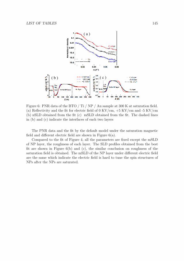
LIST OF TABLES 145
( a )
( b ) ( c )
Figure 6: PNR data of the BTO / Ti / NP / Au sample at 300 K at saturation field.(a) Reflectivity and the fit for electric field of 0 KV/cm, +5 KV/cm and -5 KV/cm(b) nSLD obtained from the fit (c) mSLD obtained from the fit. The dashed linesin (b) and (c) indicate the interfaces of each two layers
The PNR data and the fit by the default model under the saturation magneticfield and different electric field are shown in Figure 6(a).
Compared to the fit of Figure 4, all the parameters are fixed except the mSLDof NP layer, the roughness of each layer. The SLD profiles obtained from the bestfit are shown in Figure 6(b) and (c), the similar conclusion on roughness of thesaturation field is obtained. The mSLD of the NP layer under different electric fieldare the same which indicate the electric field is hard to tune the spin structures ofNPs after the NPs are saturated.

146 LIST OF TABLES
G. PNR Fit parameters by two models
The parameter of the PNR fits are presented in the following tables.
Table 1: PNR 300 K at saturation field and E = 0 KV/cm
ParameterSpherical model Default model
Value Fit Value Fit
Denssub 0.05946 atom/A3 True 0.05493 atom/A3 TrueSigsub 13.01296 A True 20.99000 A TrueThAu 36.69360 A True 157.22000 A True
DensAu 0.07363 atom/A3 True 0.03250 atom/A3 TrueSigAu 0.45627 A True 1.52040 A TrueThT i 75.00000 A True 52.76200 A True
DensT i 0.00206 atom/A3 True 0.003000 atom/A3 TrueSigT i 10.32880 A True 13.2550000 A True
ThFiMlayer ∗1 250.93593 A True 158.9300 A TrueSigFiMlayer 1.34625 A True 35.14900 A True
maxDensFiMlayer 0.08544 atom/A3 True 0.00918 atom/A3 TrueminDensFiMlayer 0.00414 atom/A3 True \ \
MagFiMlayer 1.00602 µB/atom True 1.22420 µB/atom TrueMagangleFiMlayer 62.82374 degree True 47.99685 degree True
Sigsphere 4.37180 A True \ \Slices 39 True \ \
∗1 ’FiMlayer’ with respect to the default model hereby and in the following indicate the layer (Fe2O3)0.8 (Fe3O4)0.15(FexO)0.05 while it indicate the layer 0.7((Fe2O3)0.8 (Fe3O4)0.15 (FexO)0.05) · 0.3 Au with respect to the sphericalmodel.Denssub indicates the atomic density, the nuclear scattering length density is calculated by atomic density timesnuclear scattering length. Sigsub represents the roughness of the BTO substrate.ThAu, DensAu and SigAu indicates the thickness, the nuclear scattering density and roughness of the Au layerThe same parameters apply for Ti layer.For FiM layer, Slices indicates the number of slices averagely divided in fitting process. The maxDensFiMlayer andminDensFiMlayer in spherical model in used to give the gradient of the nuclear scattering density of the slices underthe spherical function. MagFiMlayer indicates the magnetic scattering density of the FiM layer. MagangleFiMlayer
represents direction of the magnetic moment with respect to the in-plane x-axis.

LIST OF TABLES 147
Table 2: PNR 300 K at coercive field and E = 0 KV/cm
ParameterSpherical model Default model
Value Fit Value Fit
Denssub 0.05946 atom/A3 False 0.05493 atom/A3 FalseSigsub 13.01296 A False 20.99000 A FalseThAu 36.69360 A False 157.22000 A False
DensAu 0.06519 atom/A3 True 0.016899 atom/A3 TrueSigAu 1.00538 A True 0.013549 A TrueThT i 75.00000 A False 52.76200 A False
DensT i 0.00206 atom/A3 False 0.003000 atom/A3 FalseSigT i 10.45924 A True 13.2550000 A True
ThFiMlayer 250.93593 A False 158.9300 A FalseSigFiMlayer 0.64299 A True 35.14900 A True
maxDensFiMlayer 0.08544 atom/A3 False 0.00918 atom/A3 FalseminDensFiMlayer 0.00414 atom/A3 False \ \
MagFiMlayeru 0.36963 µB/atom True 1.18500 µB/atom TrueMagangleFiMlayer 65.71860 degree True 37.09585 degree True
Sigsphere 4.51679 A True \ \Slices 45 True \ \
Table 3: PNR 300 K at coercive field and E = +5 KV/cm
ParameterSpherical model Default model
Value Fit Value Fit
Denssub 0.05946 atom/A3 False 0.05493 atom/A3 FalseSigsub 3.99891 A True 20.99000 A TrueThAu 36.69360 A False 157.22000 A False
DensAu 0.04524 atom/A3 True 0.016899 atom/A3 FalseSigAu 8.00050 A True 12.52170 A TrueThT i 75.00000 A False 52.76200 A False
DensT i 0.00206 atom/A3 False 0.003000 atom/A3 FalseSigT i 3.69725 A True 0.73500 A True
ThFiMlayer 250.93593 A False 158.9300 A FalseSigFiMlayer 9.17690 A True 38.26950 A True
maxDensFiMlayer 0.08544 atom/A3 False 0.00918 atom/A3 FalseminDensFiMlayer 0.00414 atom/A3 False \ \
MagFiMlayer 0.30116 µB/atom True 0.98005 µB/atom TrueMagangleFiMlayer 74.72129 degree True 15.09585 degree True
Sigsphere 4.34233 A True \ \Slices 45 True \ \

148 LIST OF TABLES
Table 4: PNR 300 K at coercive field and E = -5 KV/cm
ParameterSpherical model Default model
Value Fit Value Fit
Denssub 0.05946 atom/A3 False 0.05493 atom/A3 FalseSigsub 3.59275 A True 20.99000 A FalseThAu 36.69360 A False 157.22000 A False
DensAu 0.04419 atom/A3 True 0.016899 atom/A3 FalseSigAu 0.04400 A True 11.69180 A TrueThT i 75.00000 A False 52.76200 A False
DensT i 0.00206 atom/A3 False 0.003000 atom/A3 FalseSigT i 2.61132 A True 0.60500 A True
ThFiMlayer 250.93593 A False 158.9300 A FalseSigFiMlayer 7.31541 A True 39.15760 A True
maxDensFiMlayer 0.08544 atom/A3 False 0.00918 atom/A3 FalseminDensFiMlayer 0.00414 atom/A3 False \ \
MagFiMlayer 0.23356 µB/atom True 0.945105 µB/atom TrueMagangleFiMlayer 79.50890 degree True 17.13585 degree True
Sigsphere 4.42618 A True \ \Slices 42 True \ \
Table 5: PNR 300 K at saturation field and E = +5 KV/cm
ParameterSpherical model Default model
Value Fit Value Fit
Denssub 0.05946 atom/A3 False 0.05493 atom/A3 FalseSigsub 3.79997 A True 21.05420 A TrueThAu 36.69360 A False 157.22000 A False
DensAu 0.04519 atom/A3 True 0.03250 atom/A3 TrueSigAu 6.00001 A True 16.30140 A TrueThT i 75.00000 A False 52.76200 A False
DensT i 0.00206 atom/A3 False 0.003000 atom/A3 FalseSigT i 3.05024 A True 0.62500 A True
ThFiMlayer 250.93593 A False 158.9300 A FalseSigFiMlayer 6.24733 A True 29.24690 A True
maxDensFiMlayer 0.08544 atom/A3 False 0.00918 atom/A3 FalseminDensFiMlayer 0.00414 atom/A3 False \ \
MagFiMlayer 0.35097 µB/atom True 1.248082 µB/atom TrueMagangleFiMlayer 57.44762 degree True 13.45870 degree True
Sigsphere 4.11567 A True \ \Slices 57 True \ \

LIST OF TABLES 149
Table 6: PNR 300 K at saturation field and E = -5 KV/cm
ParameterSpherical model Default model
Value Fit Value Fit
Denssub 0.05946 atom/A3 False 0.05493 atom/A3 FalseSigsub 3.76461 A True 21.05420 A TrueThAu 36.69360 A False 157.22000 A False
DensAu 0.04524 atom/A3 True 0.03250 atom/A3 TrueSigAu 0.13446 A True 15.16400 A TrueThT i 75.00000 A False 52.76200 A False
DensT i 0.00206 atom/A3 False 0.003000 atom/A3 FalseSigT i 3.28260 A True 0.62500 A True
ThFiMlayer 250.93593 A False 158.9300 A FalseSigFiMlayer 7.24733 A True 28.54590 A True
maxDensFiMlayer 0.08544 atom/A3 False 0.00918 atom/A3 FalseminDensFiMlayer 0.00414 atom/A3 False \ \
MagFiMlayer 0.36202 µB/atom True 0.903805 µB/atom TrueMagangleFiMlayer 57.58486 degree True 10.15070 degree True
Sigsphere 4.92358 A True \ \Slices 57 True \ \

150 LIST OF TABLES

Acknowledgements
I would like to sincerely thank Prof. Dr. Thomas Bruckel for leading me to thefield of neutron scattering and providing me the opportunity to work at the JulichCenter for Neutron Science, I want to thank him also for supporting me to travel todifferent places and to participate conferences and beamtimes.
I would like to thank Prof. Joachim Mayer for the efforts to accept the secondrevision of the thesis.
Special appreciations I would like to give to my supervisor Dr. Oleg Petracicfor all the support and the discussions during my thesis. I am very grateful for hispatience and the elaborate explanations in every discussion. I thank you for thecareful revisions of my thesis. The four years of research with you was fruitful andhas a profound meaning for my future scientific career.
Many thanks to Dr. Stefan Mattauch and Dr. Alexandros Koutsioumpas forthe scientific support during the neutron reflectivity measurements performed atMARIA in MLZ and especially to the discussions about the results afterwards.
Many thanks to Dr. Emmanuel Kentzinger for the help with GISAXS measure-ments, thanks to Marina Ganeva and Asma Qdemat for the help with data reductionand fitting.
I thank Berthold Schmitz for the help on the instruments.I would like to thank Prof. C. Schneider (PGI-6) for providing us the opportunity
to use their equipment.I thank XianKui Wei, Fengshan Zheng and Penghan Lu for the help with TEM,
STEM and electron holography measurements.I give my thanks to Dr. Yinguo Xiao for the help on CCMS measurements.I would like to thank all my Chinese colleges Dr. Yinguo Xiao, Xiao Sun, Wenhai
Ji, Lei Cao and Erxi Feng. Thank you for all the pleased moments we had together,the scientific atmosphere with a lot of fun was always very motivating.
I want to thank all the members of the institute JCNS-2 for both the rigorousscientific environment and a lovely research atmosphere.
Financial support from China Scholarship Council (CSC) is gratefully acknowl-edged.
Last but not least I would like to thank my parents for always supporting andencouraging me at my back.
151


Schriften des Forschungszentrums Jülich Reihe Schlüsseltechnologien / Key Technologies
Band / Volume 166 Current-Induced Magnetization Dynamics in Ferromagnetic Nanowires M. I. Khan (2018), vi, 138 ppISBN: 978-3-95806-308-2
Band / Volume 167 Management of Electrophysiological Data & Metadata Making complex experiments accessible to yourself and others L. Zehl (2018), 182 ppISBN: 978-3-95806-311-2
Band / Volume 168 Investigation of GeSn as Novel Group IV Semiconductor for Electronic Applications C. Schulte-Braucks, Christian (2018), xx, 165, XII ppISBN: 978-3-95806-312-9
Band / Volume 169 Tailoring the Electronic Properties of Epitaxial Oxide Films via Strain for SAW and Neuromorphic Applications Y. Dai (2018), VI, 133 ppISBN: 978-3-95806-319-8
Band / Volume 170 The electronic structure of transition metal dichalcogenides investigated by angle-resolved photoemission spectroscopy M. Gehlmann (2018), ii, 108, XVIII ppISBN: 978-3-95806-324-2
Band / Volume 171 Control of neuron adhesion by metal nanoparticles A. Q. Tran (2018), viii, 108 pp ISBN: 978-3-95806-332-7
Band / Volume 172 Neutron Scattering Lectures of the JCNS Laboratory Course held at Forschungszentrum Jülich and at the Heinz-Maier-Leibnitz Zentrum Garching edited by T. Brückel, S. Förster, G. Roth, and R. Zorn (Eds.) (2018), ca 300 pp ISBN: 978-3-95806-334-1
Band / Volume 173 Spin scattering of topologically protected electrons at defects P. Rüßmann (2018), vii, 230 ppISBN: 978-3-95806-336-5

Schriften des Forschungszentrums Jülich Reihe Schlüsseltechnologien / Key Technologies
Band / Volume 174 Interfacing EuO in confined oxide and metal heterostructures P. Lömker (2018), vi, 140 pp ISBN: 978-3-95806-337-2 Band / Volume 175 Operando Chemistry and Electronic Structure of Electrode / Ferroelectric Interfaces S. Gonzalez (2018), 159 pp ISBN: 978-3-95806-341-9 Band / Volume 176 Magnetic Properties of Self-assembled Manganese Oxide and Iron Oxide Nanoparticles Spin Structure and Composition X. Sun (2018), ii, 178 pp ISBN: 978-3-95806-345-7 Band / Volume 177 Model-based reconstruction of magnetisation distributions in nanostructures from electron optical phase images J. Caron (2018), XXI, 183 pp ISBN: 978-3-95806-346-4 Band / Volume 178 Simultaneous dual-color imaging on single-molecule level on a Widefield microscope and applications R. Ledesch (2018), ix, 119 pp ISBN: 978-3-95806-348-8 Band / Volume 179 Methoden der Leitfähigkeitsuntersuchung mittels Rasterkraftmikroskop und deren Anwendung auf Barium Titanat Systeme B. Reichenberg (2018), x, 144 pp ISBN: 978-3-95806-350-1 Band / Volume 180 Manipulation of magnetism in iron oxide nanoparticle / BaTiO3 composites and low-dimensional iron oxide nanoparticle arrays L. Wang (2018), VI, 151 pp ISBN: 978-3-95806-351-8
Weitere Schriften des Verlags im Forschungszentrum Jülich unter http://wwwzb1.fz-juelich.de/verlagextern1/index.asp


Schlüsseltechnologien / Key TechnologiesBand / Volume 180ISBN 978-3-95806-351-8
Schlüsseltechnologien / Key TechnologiesBand / Volume 180ISBN 978-3-95806-351-8
Manipulation of magnetism in iron oxide nanoparticle / BaTiO3 composites and low-dimensional iron oxide nanoparticle arraysLi-Ming Wang
180
Schl
üsse
ltech
nolo
gien
Ke
y Te
chno
logi
esN
anop
artic
le M
agne
to-E
lect
rics
Li-M
ing
Wan
g