Ultraviolet photoconductive sensor based on single ZnO nanowire
Upload
independentCategory
view
1download
0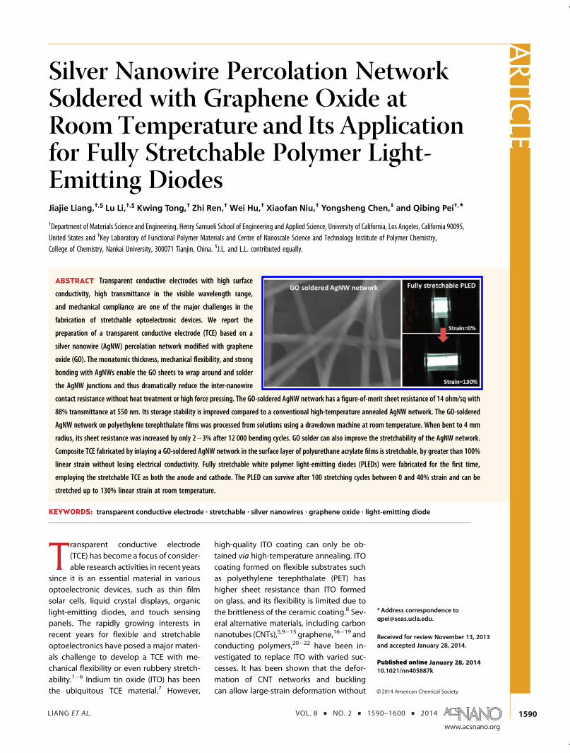
LIANG ET AL. VOL. 8 ’ NO. 2 ’ 1590–1600 ’ 2014
www.acsnano.org
1590
January 28, 2014
C 2014 American Chemical Society
Silver Nanowire Percolation NetworkSoldered with Graphene Oxide atRoomTemperature and Its Applicationfor Fully Stretchable Polymer Light-Emitting DiodesJiajie Liang,†,§ Lu Li,†,§ Kwing Tong,† Zhi Ren,† Wei Hu,† Xiaofan Niu,† Yongsheng Chen,‡ and Qibing Pei†,*
†Department of Materials Science and Engineering, Henry Samueli School of Engineering and Applied Science, University of California, Los Angeles, California 90095,United States and ‡Key Laboratory of Functional Polymer Materials and Centre of Nanoscale Science and Technology Institute of Polymer Chemistry,College of Chemistry, Nankai University, 300071 Tianjin, China. §J.L. and L.L. contributed equally.
Transparent conductive electrode(TCE) has become a focus of consider-able research activities in recent years
since it is an essential material in variousoptoelectronic devices, such as thin filmsolar cells, liquid crystal displays, organiclight-emitting diodes, and touch sensingpanels. The rapidly growing interests inrecent years for flexible and stretchableoptoelectronics have posed a major materi-als challenge to develop a TCE with me-chanical flexibility or even rubbery stretch-ability.1�6 Indium tin oxide (ITO) has beenthe ubiquitous TCE material.7 However,
high-quality ITO coating can only be ob-tained via high-temperature annealing. ITOcoating formed on flexible substrates suchas polyethylene terephthalate (PET) hashigher sheet resistance than ITO formedon glass, and its flexibility is limited due tothe brittleness of the ceramic coating.8 Sev-eral alternative materials, including carbonnanotubes (CNTs),5,9�15 graphene,16�19 andconducting polymers,20�22 have been in-vestigated to replace ITO with varied suc-cesses. It has been shown that the defor-mation of CNT networks and bucklingcan allow large-strain deformation without
* Address correspondence [email protected].
Received for review November 13, 2013and accepted January 28, 2014.
Published online10.1021/nn405887k
ABSTRACT Transparent conductive electrodes with high surface
conductivity, high transmittance in the visible wavelength range,
and mechanical compliance are one of the major challenges in the
fabrication of stretchable optoelectronic devices. We report the
preparation of a transparent conductive electrode (TCE) based on a
silver nanowire (AgNW) percolation network modified with graphene
oxide (GO). The monatomic thickness, mechanical flexibility, and strong
bonding with AgNWs enable the GO sheets to wrap around and solder
the AgNW junctions and thus dramatically reduce the inter-nanowire
contact resistance without heat treatment or high force pressing. The GO-soldered AgNW network has a figure-of-merit sheet resistance of 14 ohm/sq with
88% transmittance at 550 nm. Its storage stability is improved compared to a conventional high-temperature annealed AgNW network. The GO-soldered
AgNW network on polyethylene terephthalate films was processed from solutions using a drawdown machine at room temperature. When bent to 4 mm
radius, its sheet resistance was increased by only 2�3% after 12 000 bending cycles. GO solder can also improve the stretchability of the AgNW network.
Composite TCE fabricated by inlaying a GO-soldered AgNW network in the surface layer of polyurethane acrylate films is stretchable, by greater than 100%
linear strain without losing electrical conductivity. Fully stretchable white polymer light-emitting diodes (PLEDs) were fabricated for the first time,
employing the stretchable TCE as both the anode and cathode. The PLED can survive after 100 stretching cycles between 0 and 40% strain and can be
stretched up to 130% linear strain at room temperature.
KEYWORDS: transparent conductive electrode . stretchable . silver nanowires . graphene oxide . light-emitting diode
ARTIC
LE

LIANG ET AL. VOL. 8 ’ NO. 2 ’ 1590–1600 ’ 2014
www.acsnano.org
1591
much increase of surface conductivity.3,5,11�14 Thesecarbon or polymer-based materials have relatively lowelectrical conductivity, and the sheet resistances ofcorresponding TCE are 1�2 orders of magnitude high-er than that of ITO/glass.17,23 Percolation networks ofsilver nanowires (AgNWs) have shown promise to rivalITO/glass in sheet resistance and visual transpar-ency.24�27 Due to the high conductivity of silver, thesheet resistance of a AgNW percolation network isdominated by the contact resistance of inter-nanowirejunctions.28,29 Postprocessing treatments, such ashigh-temperature annealing (normally higher than180 �C),24,30,31 high-force pressing,26,32�34 and plasmo-nic welding,28 are effective in reducing the junctionresistance by fusing the AgNW junctions. A number ofworks have employed AgNW networks to fabricatestretchable TCE.23,35�39 However, the stretchability ofthese AgNW networks is limited because, under largetensile deformation, the nanowire junctions coulddetach and the nanowires slide against each other tocause high contact resistance that cannot be fullyrecovered when the stretched material is relaxed toits original shape.Introducing a second functional component into the
AgNWnetwork to forge inter-nanowire connection hasbeen reported as a promising technique to reduce thesheet resistance of AgNW networks.40�43 Lee et al.
used poly(3,4-ethylenedioxythiophene):poly(styrene-sulfonate) (PEDOTE:PSS) as a soldering material tomake a AgNW/PEDOT:PSS hybrid composite elec-trode.41 The stretchability of this hybrid electrode isrelative low, and the PEDOT:PSS could uptake environ-mental water and cause corrosion of the AgNWs.42
During the preparation of this article, Lee et al. reportedintegrating AgNW networks onto chemical vapor de-posited (CVD) graphene to make a graphene�AgNWhybrid that exhibits high optical-electrostretchableperformance.43 This approach does not appear to becompatible with large-area, low-cost processing thathas been one of the major motivations for using theAgNW-based TCE.Herein, we report the preparation of a highly con-
ductive AgNW and graphene oxide (GO) hybrid net-work by all-solution processing at room temperature.GO, amonatomic layer thick two-dimensional material,was chosen as a soldering material for AgNW junctionsbased on the following considerations: (1) GO containsa large number of oxygen-containing groups, suchas hydroxyl, epoxide, diol, ketone, and carboxyl, thatcould forge strong bonding with AgNWs; (2) it hasan extremely high Young's modulus (∼0.25 TPa)and a high flexibility, making it an extremely toughmaterial; and (3) GO is inexpensive and solution-processable.44�47 The charged and flexible GO sheetsin solution could adhere and wrap around the AgNWsand solder the inter-nanowire junctions, causingsignificant reduction of the inter-nanowire contact
resistance without heat treatment or high-force press-ing. The GO-AgNW network thus can be formed onpolyethylene terephthalate (PET) with high optical-electrical performance and mechanical flexibility. Thestrong bonding and high toughness of GO could alsoknot-tie the AgNWnetworks to prevent inter-nanowiresliding and thus allow reversible large-strain deforma-tion. Stretchable TCE based on the GO-soldered AgNWnetwork inlaid in the surface layer of polyurethaneacrylate (PUA) shows rubbery stretchability while re-taining its high electrical conductivity. Furthermore,fully stretchable white polymer light-emitting diodes(PLEDs) have also been demonstrated for the first timeusing this stretchable TCE as both the anode and thecathode.
RESULTS AND DISCUSSION
The process to fabricate a GO-AgNW network, asillustrated in Figure 1a, started with bar-coating a layerof AgNWs on a glass substrate from a dispersion inisopropyl alcohol (IPA) using a drawdown machine.Figure 1b displays an optical photograph of an as-prepared AgNW network with 20 � 15 cm2 area on aglass substrate. Sheet resistance and transmittanceof the AgNW coating was determined by the coatingdensity (mg/m2) of the AgNW percolation networkwhich is controlled via the concentration of the AgNWink, as detailed in theMethods section. The dried AgNWcoating was subsequently soaked into a 1 mg/mL GOdispersion in distilledwater and IPA for severalminuteswithout any heating or stirring. The AgNW coating wasthen rinsed with distilled water repeatedly and blow-dried. All of these procedures were solution-based andcarried out at room temperature.The microstructure of the resulting GO-AgNW net-
work was imaged by scanning electron microscopy(SEM), as shown in Figure 1c. The AgNW junctions arewrapped and soldered by GO sheets. SEM image inFigure S1 (Supporting Information) further depicts thatalmost all the AgNW junctions in the network aresoldered by GO sheets. The GO-soldered junctionsare quite different from those fused through thermalheating (Figure 1d, 180 �C annealed for 30 min). Thesoldered junctions are also different from those usinggraphene or GO/AgNW hybrids, wherein the grapheneor GO sheets covered like a blanket on top of the AgNWnetworks.29,40,43,48 In our process, the soldering ofAgNW junctions by GO is result of (1) the uniqueproperties of GO, including various oxygen-containingfunctional groups present on the surface and the out-standing mechanical strength and flexibility, and (2)the process of soaking AgNW networks in a GO solu-tion. When the AgNW networks are soaked in a GOdispersion, the charged GO sheets tend to bond withthe AgNWs and AgNW junctions due to the strongelectrostatic adhesion. The flexibility of the GO sheetsallows them to conform around the AgNW junctions
ARTIC
LE

LIANG ET AL. VOL. 8 ’ NO. 2 ’ 1590–1600 ’ 2014
www.acsnano.org
1592
like a plastic wrap. The rinsing process washed off theGO sheets that do not bond strongly with AgNWs.Blow-drying the GO-AgNW coating facilitates the GOsheets to wrap around the AgNW junctions and knot-tie the junctions due to electrostatic forces as well ascapillary force during the evaporation of solvent mol-ecules between the GO and AgNWs. The GO sheetshave high toughness and act as a soldering materialwhen wrapped around the AgNW junctions. Knot-tying the AgNW junctions can not only reduce theinter-nanowire contact resistance but also preventinter-nanowire sliding at the junctions. This will befurther discussed below.The sheet resistance of the GO-AgNW networks as a
function of soaking time in GO solution is depicted inFigure 2a. The sheet resistance can be greatly loweredfrom1045 to 26 and 20 ohm/sq after just 30 s and 1minsoaking time, respectively. In 5 min of soaking, theGO-AgNW network reaches a low sheet resistance of14 ohm/sq. Prolonged soaking does not considerablylower the sheet resistance. In comparison, thermaltreatment to fuse the AgNW junctions usually takesmore than 30 min to complete.24,30,31
The sheet resistance and transparency of theGO-AgNW networks are dependent on the coatingdensity of AgNWs. Figure 2b shows the results for threerepresentative GO-AgNW networks with three AgNWdensities: D1, 85 mg/m2; D2, 127 mg/m2; and D3,170 mg/m2. Their sheet resistance and transmittanceat 550 nm are 26, 14, and 12 ohm/sq and 92.1, 88.2, and86.0%, respectively. Figure 2c compares the optical-electroperformance of the GO-AgNW networkswith important TCEs published in the literature and
commercial ITO. It can be seen that the GO-AgNWnetworks fabricated through solution-based processat room temperature conditions exhibit comparableelectro-optical performance to commercial ITO coatedon glass, significantly higher performance than ITO/PET(a commercial material widely used for flexible optoe-lectronic devices), and higher performance than mostof the new TCE intended to replace ITO. Furthermore,the GO-AgNW networks are also superior to most ther-mally treated or hot-pressed AgNW networks, and theonly AgNW network that exhibits lower sheet resis-tance with higher transmittance is that made up ofnanowires with extremely long length.27
Supporting Information Figure S2 shows the trans-mittance spectra of AgNW networks with three differ-ent coating densities, D1, D2, and D2, treated by eitherGO soldering (GO-AgNW) or high-temperature anneal-ing at 180 �C for 30 min (named HT-AgNW; the an-nealing condition was optimized in our previousstudy).30,31,39 At the same AgNW densities, GO-AgNWand HT-AgNW networks show almost identical trans-mittance. This result indicates that there are little GOsheets located in the optical pathway unblocked byAgNWs; that is, almost all GO sheets present in thecoating wrap around the AgNWs and AgNW junctionsand add little to total optical loss of the coating. Thisanalysis is consistent with the SEM observation shownin Figure 1c. TheGO-AgNWnetworks are different fromthe reported CVD graphene/AgNW coatings where thegraphene sheets cover the AgNW network like ablanket.41
Figure 3a compares the sheet resistance of GO-AgNW and HT-AgNW networks at the same AgNW
Figure 1. (a) Schematic illustration of the fabrication of a GO-AgNW network on a glass substrate at room temperature. (b)Optical photograph of a AgNW network (20 � 15 cm2) bar-coated on a drawdown machine. SEM images of (c) GO-solderedAgNW junctions (indicated by red arrows) and (d) typical high-temperature fused AgNW junctions.
ARTIC
LE

LIANG ET AL. VOL. 8 ’ NO. 2 ’ 1590–1600 ’ 2014
www.acsnano.org
1593
densities. One interesting trend to note is that, at lowAgNWdensity (D1), GO-AgNW ismore conductive thanHT-AgNW. At high density (D3), HT-AgNW is moreconductive. One plausible explanation is that, at lowdensities, AgNWs are sparsely distributed. The bindingforce of GO helps move nearby AgNWs to form lowresistance joints. At high AgNW density, AgNW junc-tions are abundant, and the fusing between AgNWsbecomes much more effective to lower the junctionresistance than GO soldering does without thermaltreatment.The GO-AgNW and HT-AgNW networks show differ-
ent storage stability. Figure 3b displays the resistancechange of the networks during accelerated test at85 �C in air. The sheet resistance of the HT-AgNWnetwork increases by 5% in 1 day. Longer heating upto 8 days total does not further increase the resistance.In contrast, the sheet resistance of the GO-AgNW
network increases by a mere ∼0.4% in 8 days. Thesheet resistance increase of AgNW networks has beenreported in the literature and attributed to attacks byenvironmental oxygen and sulfur which can signifi-cantly increase the junction resistance.40,43 Graphenesheets have been shown to be an excellent barriermaterial. We suggest that GO wrapping around theAgNW junctions can impede the environmental oxi-dants from oxidizing the AgNWs and their junctionsand increase the stability for the GO-AgNW networks.ITO coated on PET is widely used in industry for
flexible optoelectronic devices. The flexibility ofITO/PET films are rather limited; strain of 1% or largercan cause irreversible crack formation in the ITO.31
AgNWnetwork coated on a plastic substrate is a widelyinvestigated alternative material. However, the con-ventional approach of fusing AgNWs at elevated tem-peratures is only applicable to high-temperaturesubstrates. The solution-based room temperature pro-cessing allows the formation of GO-AgNWnetworks onmuch more polymer-based substrates, such as PET,polyethylene naphthalate, and polyacrylate. Figure 4adisplays a sheet of GO-AgNW/PET with an area of20 � 40 cm2 and sheet resistance of 26 ( 5 ohm/sq(the error range indicates the variation of local sheetresistance and is insignificant for most applications).Mechanical flexibility of a GO-AgNW/PET film wasevaluated by repeated bending to a radius of 4 mmusing a linear stretcher built in house (Figure 4b). The
Figure 2. (a) Measured sheet resistance of a GO-AgNWnetwork as a function of the soaking time in a GO solution.(b) Transmittance spectra of GO-AgNWnetworks with threedifferent AgNW densities (D1, D2, and D3). (c) Comparisonof the electro-optical performance of the GO-AgNW net-works with various TCE films published in the literature andcommercial ITO/glass and ITO/PET (all data are exclusive ofsubstrate).
Figure 3. (a) Comparison of sheet resistance of GO-AgNWnetworks with HT-AgNW networks. (b) Plots of the relativesheet resistance change versus time for GO-AgNWnetworksand HT-AgNWnetworks with the sameAgNWdensities (D2)after exposure to hot air (85 �C) for 8 days.
ARTIC
LE

LIANG ET AL. VOL. 8 ’ NO. 2 ’ 1590–1600 ’ 2014
www.acsnano.org
1594
moving speed of the stretcher was set at 50 mm/s.During 12 000 cycles of bending�unbending, the re-sistance of the GO-AgNW network remained relativelystable (Figure 4c). It increased by merely 2�3%, reveal-ing good flexibility of the GO-AgNW network. More-over, this GO-AgNW/PET (26 ohm/sq) also shows betterelectro-optical performance than the commercialITO/PET film (35 ohm/sq, obtained from Aldrich), asshown in Figure S3.The GO-AgNW networks were also employed to
fabricate a stretchable transparent composite elec-trode by an in situ substrate polymerization and trans-fer technique that we have previously reported forHT-AgNW networks.5,37,49 A urethane acrylate mono-mer was coated onto the GO-AgNW network on areleasing glass substrate. The monomer was cured,and the resulting PUA film was peeled off to transferthe GO-AgNW network into the surface layer of thePUA film. Figure 5a shows the transmittance spectra ofthe GO-AgNW/PUA composite electrodes with threeAgNW densities (D1, D2, and D3). The transmittance at550 nm is 86.3, 82.5, and 79.2% for composite electro-des with sheet resistances of 26, 14, and 12 Ω/sq,respectively. It should be noted that the transmittancedata are inclusive of the PUA matrix, while the datareported in many published papers are for AgNWcoating only. In order to test the stretchability of thetransparent composite electrodes, samples with di-mensions of 20 mm in length and 5 mm in width weremounted on a motorized linear stage, leaving a 5 mmlength (gauge length) free to deform. All samples werestretched at 1 mm/s (strain rate: 20%/s), and theresistance was monitored in sync with the stretching.Figure 5b displays the normalized resistance (R/R0, theratio of the instantaneous resistance at a specifictensile strain to the initial resistance at zero strain) forthe GO-AgNW/PUA and HT-AgNW/PUA compositeelectrodes. Both electrodes have the same AgNWdensities (D2) and the same initial sheet resistance(14 ohm/sq). More than five samples of each electrodewere tested, and the variation of resistance amongthe samples in each group was within (10%. The GO-AgNW/PUA electrode shows much smaller resistance
increase with strain than the HT-AgNW/PUA electrode.The resistance increase of the GO-AgNW/PUA is3.2-, 5.3-, and 10.6-fold at strains of 40, 60, and 80%,respectively; in comparison, the increase is 5.4, 9.8, and17.2, respectively, for the HT-AgNW/PUA.The difference in stretchability between the GO-
AgNW/PUA and HT-AgNW/PUA is also shown in re-peated stretching�relaxing (Figure 6a,b). During 100cycles of stretching�relaxing between 0 and 20%strains, the peak of the resistance change (at 20%strain) for GO-AgNW/PUA increases very graduallyfrom about 2.3 to 2.7 times its initial value; as for theHT-AgNW/PUA, the peak resistance increases from2.9 to 3.3 times its initial value. During the cyclic tests
Figure 4. (a) Optical photograph of a GO-AgNW/PET sheet (26 ohm/sq) coated on a drawdown machine (coating area: 20 �40 cm2). (b) Optical photograph of a GO-AgNW/PET bent to 4mm radius. (c) Relative resistance change of the GO-AgNW/PETduring repeated bending�unbending test (bending radius: 4 mm).
Figure 5. (a) Transmittance spectra of GO-AgNW/PUA com-posite electrodes with specified sheet resistance. (b) Nor-malized resistance of the 14 ohm/sq GO-AgNW/PUAcomposite electrodes and 14 ohm/sq HT-AgNW/PUA com-posite electrodes as a function of tensile strain (strain rate is1 mm/s).
ARTIC
LE

LIANG ET AL. VOL. 8 ’ NO. 2 ’ 1590–1600 ’ 2014
www.acsnano.org
1595
between 0 and 40% strain, the peak resistance of GO-AgNW/PUA increases fromabout 3.4 to 4.8 times its initialvalue in 100 cycles, while that of the HT-AgNW/PUAincreases from 6.0 to 8.5 times its initial value. Theresults indicate fairly high stretching reversibility forboth electrodes, but the GO-AgNW/PUA clearly showshigher stability as indicated by the smaller width of theribbons (the shaded area formed between the peakand trough resistances in Figure 6a,b).For bulk conductive material, its resistance increases
with strain following the equation R/R0 = (1 þ strain)2
due to geometrical changes (elongation in length andshrinking in width due to Poisson's law).38,50,51 For anideal network formed by conductive nanowires inwhich the nanowire junctions are intact during stretch-ing, like a fishnet (Figure 6c), the geometrical changesduring a uniaxial stretching should not cause anysignificant resistance increase. The macroscopic elon-gation of the network would cause stress around thejunctions and possible buckling or twisting of thenanowires. The corresponding change in macroscopicresistance should be small as the conduction pathwaysalong the nanowires remainmore or less the same. Theloss of surface conductivity of HT-AgNW networks
under large tensile strain has been considered to becaused in large by the loss of interconnection betweenthe nanowires.23 The thermal-fused AgNW junctionsmay be easily broken under twisting stress. Embeddingthe HT-AgNW networks in an elastomeric matrix, suchas in the composite electrodes of HT-AgNW/PUA, canlimit the degree of junction disjointing and nanowiresliding.35,38,39,49 The elastomeric matrix can help distrib-ute the stress more uniformly. In the GO-AgNW/PUAcomposite electrode, wrapping of the junctions by theflexible yet very tough GO sheets can allow the twist ofGO-soldered AgNW junctions and prevent the disjoint-ing or sliding of AgNW nanowires against each otherduring large-strain deformation. Stretchability of theGO-AgNW networks is thus improved. However, com-pared to the fishnet model in Figure 6c, the silvernanowires are not sufficiently stretchable and tough.Large-strain deformation can still cause macroscopicresistance increase, and some of the increase is irre-versible, and disjointing, sliding, and even fracturecould still occur, albeit at a smaller extent comparedto what has been reported in literature.37�39,41
We have reported the fabrication of fully stretchablepolymer light-emitting electrochemical cells (PLEC) by
Figure 6. Normalized transient resistance of GO-AgNW/PUA and HT-AgNW/PUA composite electrodes during 100 cycles oftensile stretching and releasing between 0 and 20% strains (a) and 0 and 40% strains (b). The initial sheet resistances of bothelectrodes are 14 ohm/sq. The stretching speed is 1 mm/s. (c) Schematic illustration of the deformation of an ideal nanowirenetwork wherein the nanowire junctions are intact during uniaxial stretching.
ARTIC
LE

LIANG ET AL. VOL. 8 ’ NO. 2 ’ 1590–1600 ’ 2014
www.acsnano.org
1596
sandwiching a thin film of a blend of luminescentconjugated polymer, an ionic conductor, and lithiumsalt between a pair of composite electrodes.5,49 Thecomposite electrodes comprise a thin percolation net-work of HT-AgNWs or SWCNTs in the surface layer ofthe polymer substrate. With the use of shape memorypolymer or elastomeric polymer as the substrate, thePLECs are fully stretchable, wherein all components areelongated as the thin film devices are stretched.5,6,49
These stretchable PLECs suffer from such problems asslow turn-on and short lifetime at high brightness thatare quite characteristic for PLECs.52,53 To evaluate theapplication potential of the GO-AgNW/PUA compositeelectrode for fully stretchable white PLED, the electro-luminescence of which does not require the in situ
formation of a p-i-n junction as in the PLECs, light-emitting diodes were fabricated by solution-basedcoating and lamination process. Atom force micro-scope measurement showed that the height variationof the GO-AgNW/PUA composite electrode surfaceis around 10 nm (Figure S4), which is suitable forthe fabrication of a PLED. The devices have a thinfilm sandwich structure of GO-AgNW/PUA/poly(3,4-ethylenedioxythiophene):poly(styrenesulfonate)(PEDOT:PSS)/emissive polymer layer/polyethylenimine(PEI)/GO-AgNW/PUA, as illustrated in Figure 7a. In anutshell, the solution-based fabrication process started
spin-coating a PEDOT:PSS layer on GO-AgNW/PUA asthe hole transporting layer (HTL); the emissive layer(EL), consisting of a white-light-emitting polymer and1,3-bis[(4-tert-butylphenyl)-1,3,4-oxidiazolyl]pheny-lene (OXD-7) mixed at weight ratio of 100:10, was thenspin-coated on top of the HTL. On a second GO-AgNW/PUA, polyethylenimine (PEI), 5 nm thick, was coated asthe electron transporting layer (ETL) to enhance elec-tron injection.54 The two GO-AgNW/PUA films werelaminated with the conductive layers facing eachother. The sheet resistance of the GO-AgNW/PUA com-posite electrodes used was 14 ohm/sq. Thesematerialswere selected for stretchability of the resulting PLEDs.The composition and layer thicknesswere preliminarilyoptimized for overall performance in electrolumines-cent and stretchability.The characteristic current density�brightness�
driving voltage responses (J�B�V) and current effi-ciency�brightness curves (η�L) of the PLED are mea-sured as shown in Figure 7c,d. Leakage current can beseen from 1 to 6 V in the J�B�V curve, which could becaused by the surface roughness of composite electro-des or defects introduced during the lamination pro-cess. The electroluminescence turns on at around 7 Vand reaches a brightness of 1100 cd/m2 at 21 V. Themaximum current efficiency is 2.0 cd/A obtained at thebrightness of 571 cd/m2. Figure 7b shows an undriven
Figure 7. (a) Schematic drawing of a fully stretchable PLED using GO-AgNW/PUA composite electrode as both anode andcathode. (b) Optical photographs of a semitransparent unlit stretchable PLED (top) and a stretchable PLED operated at 13 Vemitting white light from two sides and illuminating two white papers with printed ULCA logo in black (bottom). (c) Currentdensity�luminance�driving voltage characteristics and (d) current efficiency�brightness characteristics of the PLED device.(e) Optical photographs of a PLED (original lighting area: 3mm�4mm)beingdriven at 14V and stretched to specified strains.
ARTIC
LE

LIANG ET AL. VOL. 8 ’ NO. 2 ’ 1590–1600 ’ 2014
www.acsnano.org
1597
semitransparent PLED and a driven PLED emittingwhite light from both sides. The light emitted fromeither side of the transparent PLED has almost identicalJ�B�V and η�L responses, as shown in Figure S5.Therefore, the actual emission intensity and efficiencyof the PLEDs are twice as much as shown in Figure 7,and the maximum current efficiency is 4.0 cd/A.49,55
The CIE coordinates of the emission color are de-picted in Figure S6 on the Commission Internationalede L'Eclairage (CIE) 1931 chromaticity coordinatesdiagram. At the emission brightness of 100, 500, and1000 cd/m2, measured from one side of the devices,the color coordinates are (0.35, 0.35), (0.33, 0.34), and(0.31, 0.34), respectively, all being fairly close to purewhite (0.33, 0.33). More importantly, the PLEDs are softand stretchable at room temperature. As shown inFigure 7e, the PLED with a lighting area of 3 � 4 cm2
can be stretched by as large as 130% linear strain whiledriven at 14 V. The emission intensity is fairly uniformacross the entire lit area.The supplementary video clip (Supporting Information)
demonstrates stretching operation of a PLED andshows a fairly uniform and bright light emission duringstretching�releasing cycles. Figure 8 demonstratesthe current density�driving voltage (I�V), bright-ness�driving voltage (B�V), and current efficiency�brightness (η�B) characteristic curves of PLED after10, 50, and 100 cycles of stretching�relaxing between0 and 20% strains (Figure 8a�c) and between 0 and40% strains (Figure 8d�f). The leakage current, whichis clearly seen from the I�V curves for the originalPLEDs, is largely suppressed after the stretching�releasing cycles. The brightness�voltage and current
efficiency�brightness curves both exhibit a decliningtrend with increasing stretching�releasing cycles.However, the turn-on voltage of the stretched PLEDsdoes not change much with stretching�releasingcycles. The current efficiency gradually increases witheach additional stretching�releasing cycle. For in-stance, for a fresh PLED with a current efficiency of1.5 cd/A at 280 cd/m2, its current efficiency is increasedto 2.1 cd/A at the same brightness after 100 cycles ofstretching�releasing between 0 and 40%. This increas-ing efficiency may be consistent with the decreasingleakage current. There could be other factors thatcould affect the efficiency of the stretchable PLEDsafter stretching. Charging injection interfaces, thick-ness of the emissive layer, molecular orientation, andmorphological changes could all play an importantrole in the electroluminescence. Substantial efforts arerequired to fully optimize the mechanical and electro-luminescent properties of the PLEDs.
CONCLUSIONS
In summary, the GO sheet is a useful material tosolder AgNW junctions. Immersing the AgNW coatingin GO solutions leads to deposition of GO sheets towrap around the nanowires and their junctions. Thereis little deposition of GO sheets in the substrate surfaceareas uncovered by the nanowires, which allow for thedecrease in sheet resistance of the network withoutsignificant lost of optical transmittance. The highlyconductive and transparent GO-AgNW networks couldbe formed on flexible substrates such as PET via an all-solution-based process at room temperature. The ob-tained GO-AgNW networks exhibit high mechanical
Figure 8. (a) Current density�driving voltage, (b) brightness�driving voltage, and (c) current efficiency�brightnesscharacteristics of a stretchable PLED after specified stretching�relaxing cycles between 0 and 20% strains. (d) Currentdensity�driving voltage, (e) brightness�driving voltage, and (f) current efficiency�brightness characteristics of a stretchablePLED after specified stretching�relaxing cycles between 0 and 40% strains.
ARTIC
LE

LIANG ET AL. VOL. 8 ’ NO. 2 ’ 1590–1600 ’ 2014
www.acsnano.org
1598
flexibility. When embedded in the surface layer of theelastomeric PUA, the transparent composite elec-trode behaves like a rubbery substance at roomtemperature. The films could be stretched repeatedlyto 40% strains due to the strong bonding of the GOsheets on the junctions to prevent disjointing orsliding of the nanowires against each other duringlarge-strain deformation. The rubbery compositeelectrode was used successfully to demonstrate, forthe first time, fully stretchable polymer light-emittingdiodes that could be stretched by as much as 130%
and repeatedly by 40%. Large-strain deformation cancause a lot of interesting changes in materials, includ-ing interfacial bonding, charge injection barriers,molecular orientation, and morphological changesin neat materials and blends. These changes canaffect the stretchability and electroluminescent prop-erties of PLEDs. Therefore, there are plenty of para-meters to adjust to optimize the performance of thestretchable PLEDs. Meanwhile, these devices shouldalso provide unique opportunities to investigate thematerials properties in situ.
METHODS
Raw Materials. AgNWs were synthesized according to areported procedure.5,56 GO was prepared from graphite bythe modified Hummers method.44,46 Siliconized urethaneacrylate oligomer (UA) and an ethoxylated bisphenol Adimethacrylate (EBA) were supplied by Sartomer. 2,2-Di-methoxy-2-phenylacetophenone (photoinitiator), anhydrouschlorobenzene, and polyethylenimine (PEI), 80% ethoxylatedsolution (35�40 wt % in H2O, average Mw ∼70 000), were allobtained from Sigma-Aldrich. Low conductivity poly(3,4-ethylenedioxythiophene):poly(styrenesulfonate) (PEDOT:PSS)(Clevios VP Al4083) was purchased from H.C. Starck Inc. Thewhite-light-emitting polymer was provided by Cambridge Dis-play Technology. 2-Methoxyethanol (99þ%) was bought fromAcros, and 1,3-bis[(4-tert-butylphenyl)-1,3,4-oxidiazolyl]pheny-lene (OXD-7) was obtained from Lumtech.
Preparation of GO-Soldered AgNW Networks. To fabricate the GOsolution, GO powder was first dispersed in distilled water at theconcentration of 2 mg/mL in an ultrasonic bath for 30 min. TheGO/H2O solution was diluted with isopropyl alcohol (IPA) to1 mg/mL and sonicated for an additional 30 min at roomtemperature. A glass or PET substrate was placed flat on a draw-down machine. A dispersion of AgNW in IPA was drop-castedinto a thin line at one end of the substrate and drawn downwitha Meyer rod to spread the solution to form a uniform coating.Different AgNW densities of the AgNW network on substratewas controlled by the concentration of the AgNW dispersionbeing 0.3, 0.5, and 0.7wt% to obtain AgNWnetwork densities of85 mg/m2 (D1), 127 mg/m2 (D2), and 170 mg/m2 (D3), respec-tively. The as-prepared AgNW network on substrate was thensoaked in aGOdispersion (optimized to 1mg/mL concentrationin water and IPA prepared46) for 5 min, rinsed with distilledwater, and dried. The HT-annealed AgNW network was pre-pared by heating at 180 �C for 30 min after the Meyer rodcoating on a drawdown machine.
Fabrication of Stretchable Composite Electrodes. The above GO-AgNW network and HT-AgNW network coated on releasesubstrate were subsequently overcoated with a precursor solu-tion containing 100 weight parts of UA, 20 parts of EBA, and1 part of the photoinitiator.49 The coatings were cured under UVat 2.5 W/cm2 intensity and peeled off of the release substrate.The AgNWnetwork was transferred as the conductive surface ofthe resulting transparent composite electrodes.
Fabrication of Stretchable White PLED. In a typical procedure, GO-AgNW/PUA composite electrodes were cleaned in an ultrasonicbath with detergent and distilled water for 30min each. PEDOT:PSS was first spin-coated on a composite electrode at 4000 rpmfor 60 s, baked at 70 �C for 20 min, and vacuum-dried. The driedPEDOT:PSS coating was approximately 120 nm thick, as mea-sured on a Dektak profilometer. An emissive polymer layer wasspin-coated on the PEDOT:PSS-coated electrode from a solutioncontaining a white-light-emitting polymer and OXD-7 mixed atthe weight ratio of 100:10 codissolved in chlorobenzene. Theemissive layer was 100 nm thick. A solution of PEI in methoxy-ethanol (diluted by adding 2-methoxyethanol to 0.4 wt %) wasspin-coated on another composite electrode at 5000 rpm for
60 s and dried in vacuum. The thickness of the PEI layer wasaround 5 nm. Finally, the PEI/composite electrode and theemissive polymer/PEDOT:PSS/composite electrode were lami-nated with the active materials facing each other and heated to100 �C for 3min. The lamination process was done in a gloveboxprotected with nitrogen, with oxygen, and moisture levelsbelow 0.5 ppm.
Characterization Methods. Cyclic strain testsand cyclic bending�unbending tests were performed on amotorized linear stagewithbuilt-in controller (Zaber Technologies Inc.). A Keithley 2000 digitalmultimeter was used tomonitor the resistance change. Strain andresistance datawere recordedwith a custom-made LabView code.All the electrical measurements for stretchable PLED were carriedout in the glovebox. The current�voltage�light intensity curvesfor the stretchable PLEDs in original state were measured with aKeithley 2400 sourcemeter and a calibrated silicon photodetectorby sweeping the applied voltage from 0 to 21 V at 500 mVincrements per step. The current density and brightness for thestretchable PLED under stretched state were measured utilizing aKeithley 2400 source meter and a photoresearch PR-655. All testswere carried out at room temperature. The transmittance spectrawere recorded utilizing a Shimadzu UV-1700 spectrophotometer.Scanning electron microscopy was performed on a JEOL JSM-6701F scanning electron microscope.
Conflict of Interest: The authors declare no competingfinancial interest.
Acknowledgment. The work reported here was supportedby the Air Force Office of Scientific Research (FA9550-12-1-0074). We thank Dr. Richard Wilson of Cambridge Display Tech-nology, Ltd. for supplying the white-light-emitting polymer.
Supporting Information Available: Additional figures areprovided. These include an SEM image of the GO-AgNW net-work, transmittance spectra of GO-soldered AgNW networksand HT-annealed AgNW networks on glass, transmittancespectra of GO-AgNW/PET, CIE coordinate diagram for stretch-able PLED, and a video showing a PLED under stretch-ing�releasing cycles. This material is available free of chargevia the Internet at http://pubs.acs.org.
REFERENCES AND NOTES1. Lee, S. K.; Kim, B. J.; Jang, H.; Yoon, S. C.; Lee, C.; Hong, B. H.;
Rogers, J. A.; Cho, J. H.; Ahn, J. H. Stretchable GrapheneTransistors with Printed Dielectrics and Gate Electrodes.Nano Lett. 2011, 11, 4642–4646.
2. Lipomi, D. J.; Tee, B. C. K.; Vosgueritchian, M.; Bao, Z.Stretchable Organic Solar Cells. Adv. Mater. 2011, 23,1771–1775.
3. Lipomi, D. J.; Vosgueritchian, M.; Tee, B. C. K.; Hellstrom,S. L.; Lee, J. A.; Fox, C. H.; Bao, Z. Skin-like Pressure andStrain Sensors Based on Transparent Elastic Films ofCarbon Nanotubes. Nat. Nanotechnol. 2011, 6, 788–792.
4. Park, K.; Lee, D.-K.; Kim, B.-S.; Jeon, H.; Lee, N.-E.; Whang, D.;Lee, H.-J.; Kim, Y. J.; Ahn, J.-H. Stretchable, Transparent Zinc
ARTIC
LE

LIANG ET AL. VOL. 8 ’ NO. 2 ’ 1590–1600 ’ 2014
www.acsnano.org
1599
Oxide Thin Film Transistors. Adv. Funct. Mater. 2010, 20,3577–3582.
5. Yu, Z.; Niu, X.; Liu, Z.; Pei, Q. Intrinsically Stretchable Poly-mer Light-Emitting Devices Using Carbon Nanotube�Polymer Composite Electrodes. Adv. Mater. 2011, 23,3989–3994.
6. Filiatrault, H. L.; Porteous, G. C.; Carmichael, R. S.; Davidson,G. J. E.; Carmichael, T. B. Stretchable Light-Emitting Elec-trochemical Cells Using an Elastomeric Emissive Material.Adv. Mater. 2012, 24, 2673–2678.
7. Tahar, R. B. H.; Ban, T.; Ohya, Y.; Takahashi, Y. Tin DopedIndiumOxide Thin Films: Electrical Properties. J. Appl. Phys.1998, 83, 2631–2645.
8. Cairns, D. R.; Witte, R. P.; Sparacin, D. K.; Sachsman,S. M.; Paine, D. C.; Crawford, G. P.; Newton, R. R. Strain-Dependent Electrical Resistance of Tin-Doped IndiumOxide on Polymer Substrates. Appl. Phys. Lett. 2000, 76,1425–1427.
9. Lacour, S. P.; Chan, D.; Wagner, S.; Li, T.; Suo, Z. Mechanismsof Reversible Stretchability of Thin Metal Films on Elasto-meric Substrates. Appl. Phys. Lett. 2006, 88, 204103.
10. Liu, K.; Sun, Y.; Liu, P.; Lin, X.; Fan, S.; Jiang, K. Cross-StackedSuperaligned Carbon Nanotube Films for Transparent andStretchable Conductors. Adv. Funct. Mater. 2011, 21,2721–2728.
11. Sekitani, T.; Noguchi, Y.; Hata, K.; Fukushima, T.; Aida, T.;Someya, T. A Rubberlike Stretchable Active Matrix UsingElastic Conductors. Science 2008, 321, 1468–1472.
12. Shin, M. K.; Oh, J.; Lima, M.; Kozlov, M. E.; Kim, S. J.;Baughman, R. H. Elastomeric Conductive CompositesBased on Carbon Nanotube Forests. Adv. Mater. 2010,22, 2663–2667.
13. Zhang, Y.; Sheehan, C. J.; Zhai, J.; Zou, G.; Luo, H.; Xiong, J.;Zhu, Y. T.; Jia, Q. X. Polymer-Embedded Carbon NanotubeRibbons for Stretchable Conductors. Adv. Mater. 2010, 22,3027–3031.
14. Zhu, Y.; Xu, F. Buckling of Aligned Carbon Nanotubes asStretchable Conductors: A New Manufacturing Strategy.Adv. Mater. 2012, 24, 1073–1077.
15. Geng, H. Z.; Kim, K. K.; So, K. P.; Lee, Y. S.; Chang, Y.; Lee, Y. H.Effect of Acid Treatment on Carbon Nanotube-BasedFlexible Transparent Conducting Films. J. Am. Chem. Soc.2007, 129, 7758–7759.
16. Bae, S.; Kim, H.; Lee, Y.; Xu, X.; Park, J. S.; Zheng, Y.;Balakrishnan, J.; Lei, T.; Kim, H. R.; Song, Y. I.; et al. Roll-to-Roll Production of 30-Inch Graphene Films for TransparentElectrodes. Nat. Nanotechnol. 2010, 5, 574–578.
17. Hecht, D. S.; Hu, L.; Irvin, G. Emerging Transparent Electro-des Based on Thin Films of Carbon Nanotubes, Graphene,and Metallic Nanostructures. Adv. Mater. 2011, 23, 1482–1513.
18. Kim, K. S.; Zhao, Y.; Jang, H.; Lee, S. Y.; Kim, J. M.; Kim, K. S.;Ahn, J. H.; Kim, P.; Choi, J. Y.; Hong, B. H. Large-Scale PatternGrowth of Graphene Films for Stretchable TransparentElectrodes. Nature 2009, 457, 706–710.
19. Kim, R. H.; Bae, M. H.; Kim, D. G.; Cheng, H.; Kim, B. H.; Kim,D. H.; Li, M.; Wu, J.; Du, F.; Kim, H. S.; et al. Stretchable,Transparent Graphene Interconnects for Arrays of Micro-scale Inorganic Light Emitting Diodes on Rubber Sub-strates. Nano Lett. 2011, 11, 3881–3886.
20. Argun, A. A.; Cirpan, A.; Reynolds, J. R. The First Truly All-Polymer Electrochromic Devices. Adv. Mater. 2003, 15,1338–1341.
21. Lipomi, D. J.; Lee, J. A.; Vosgueritchian, M.; Tee, B. C. K.;Bolander, J. A.; Bao, Z. Electronic Properties of TransparentConductive Films of PEDOT:PSS on Stretchable Substrates.Chem. Mater. 2012, 24, 373–382.
22. Vosgueritchian, M.; Lipomi, D. J.; Bao, Z. Highly Conductiveand Transparent PEDOT:PSS Films with a Fluorosurfactantfor Stretchable and Flexible Transparent Electrodes. Adv.Funct. Mater. 2012, 22, 421–428.
23. Lee, P.; Lee, J.; Lee, H.; Yeo, J.; Hong, S.; Nam, K. H.; Lee, D.;Lee, S. S.; Ko, S. H. Highly Stretchable and Highly Con-ductive Metal Electrode by Very Long Metal NanowirePercolation Network. Adv. Mater. 2012, 24, 3326–3332.
24. De, S.; Higgins, T. M.; Lyons, P. E.; Doherty, E. M.; Nirmalraj,P. N.; Blau, W. J.; Boland, J. J.; Coleman, J. N. Silver NanowireNetworks as Flexible, Transparent, Conducting Films: Ex-tremely High DC to Optical Conductivity Ratios. ACS Nano2009, 3, 1767–1774.
25. Gaynor, W.; Lee, J. Y.; Peumans, P. Fully Solution-ProcessedInverted Polymer Solar Cells with Laminated NanowireElectrodes. ACS Nano 2010, 4, 30–34.
26. Hu, L.; Kim, H. S.; Lee, J. Y.; Peumans, P.; Cui, Y. ScalableCoating and Properties of Transparent, Flexible, SilverNanowire Electrodes. ACS Nano 2010, 4, 2955–2963.
27. Lee, J.; Lee, I.; Kim, T. S.; Lee, J. Y. Efficient Welding of SilverNanowire Networks without Post-processing. Small 2013,9, 2887–2894.
28. Garnett, E. C.; Cai, W.; Cha, J. J.; Mahmood, F.; Connor, S. T.;Christoforo, M. G.; Cui, Y.; McGehee, M. D.; Brongersma,M. L. Self-Limited Plasmonic Welding of Silver NanowireJunctions. Nat. Mater. 2012, 11, 241–249.
29. Chen, R.; Das, S. R.; Jeong, C. W.; Khan, M. R.; Janes, D. B.;Alam, M. A. Co-percolating Graphene-Wrapped SilverNanowire Network for High Performance, Highly Stable,Transparent Conducting Electrodes. Adv. Funct. Mater.2013, 23, 5150–5158.
30. Yu, Z.; Li, L.; Zhang, Q.; Hu, W.; Pei, Q. Silver Nanowire�Polymer Composite Electrodes for Efficient Polymer SolarCells. Adv. Mater. 2011, 23, 4453–4457.
31. Yu, Z.; Zhang, Q.; Li, L.; Chen, Q.; Niu, X.; Liu, J.; Pei, Q. HighlyFlexible Silver Nanowire Electrodes for Shape-MemoryPolymer Light-Emitting Diodes. Adv. Mater. 2011, 23,664–668.
32. Gaynor, W.; Burkhard, G. F.; McGehee, M. D.; Peumans, P.Smooth Nanowire/Polymer Composite Transparent Elec-trodes. Adv. Mater. 2011, 23, 2905–2910.
33. Tokuno, T.; Nogi, M.; Karakawa, M.; Jiu, J.; Thi Thi, N.; Aso, Y.;Suganuma, K. Fabrication of Silver Nanowire TransparentElectrodes at Room Temperature. Nano Res. 2011, 4,1215–1222.
34. Yang, L.; Zhang, T.; Zhou, H.; Price, S. C.; Wiley, B. J.; You, W.Solution-Processed Flexible Polymer Solar Cells with SilverNanowire Electrodes. ACS Appl. Mater. Interfaces 2011, 3,4075–4084.
35. Feng, X. Y. Zhu. Highly Conductive and Stretchable SilverNanowire Conductors. Adv. Mater. 2012, 24, 5117–5122.
36. Ge, J.; Yao, H. B.; Wang, X.; Ye, Y. D.; Wang, J. L.; Wu, J. Y.; Liu,J. W.; Fan, F. J.; Gao, H. L.; Zhang, C. L.; et al. StretchableConductors Based on Silver Nanowires: Improved Perfor-mance through a Binary Network Design. Angew. Chem.,Int. Ed. 2013, 52, 1654–1659.
37. Yun, S.; Niu, X.; Yu, Z.; Hu, W.; Brochu, P.; Pei, Q. CompliantSilver Nanowire�Polymer Composite Electrodes for Bis-table Large Strain Actuation. Adv. Mater. 2012, 24, 1321–1327.
38. Hu, W.; Niu, X.; Zhao, R.; Pei, Q. Elastomeric TransparentCapacitive Sensors Based on An Interpenetrating Compo-site of Silver Nanowires and Polyurethane. Appl. Phys. Lett.2013, 102, 083303.
39. Hu, W.; Niu, X.; Li, L.; Yun, S.; Yu, Z.; Pei, Q. IntrinsicallyStretchable Transparent Electrodes Based on Silver-Nanowire-Crosslinked-Polyacrylate Composites. Nano-technology 2012, 23, 344002.
40. Moon, I. K.; Kim, J. I.; Lee, H.; Hur, K.; Kim, W. C.; Lee, H. 2DGrapheneOxide Nanosheets as an Adhesive Over-CoatingLayer for Flexible Transparent Conductive Electrodes. Sci.Rep. 2013, 3, 1112.
41. Lee, J.; Lee, P.; Lee, H. B.; Hong, S. K.; Lee, I.; Yeo, J.; Lee, S. S.;Kim, T. S.; Lee, D. J.; Ko, S. H. Room-Temperature Nanosol-dering of a Very Long Metal Nanowire Network by Con-ducting-Polymer-Assisted Joining for a Flexible Touch-Panel Application. Adv. Funct. Mater. 2013, 23, 4171–4176.
42. Suh, Y.; Lu, N.; Lee, S. H.; Chung, W.-S.; Kim, K.; Kim, B.;Ko, M. J.; Kim, M. J. Thin Ag Layer Induced by Poly-(3,4ethylenedioxythiophene):Polystyrene Sulfonate in aTransmission Electron Microscopy Specimen of an In-verted Polymer Solar Cell. ACS Appl. Mater. Interfaces2012, 4, 5118–5124.
ARTIC
LE

LIANG ET AL. VOL. 8 ’ NO. 2 ’ 1590–1600 ’ 2014
www.acsnano.org
1600
43. Lee,M. S.; Lee, K. S.; Kim, S. Y.; Lee, H. J.; Park, J. H.; Choi, K. H.;Kim, H. K.; Kim, D. G.; Lea, D. Y.; Nam, S. W.; et al. High-Performance, Transparent, and Stretchable ElectrodesUsing Graphene�Metal Nanowire Hybrid Structures.Nano Lett. 2013, 13, 2814–2821.
44. Dikin, D. A.; Stankovich, S.; Zimney, E. J.; Piner, R. D.;Dommett, G. H. B.; Evmenenko, G.; Nguyen, S. T.; Ruoff,R. S. Preparation and Characterization of Graphene OxidePaper. Nature 2007, 448, 457–460.
45. Gomez-Navarro, C.; Burghard, M.; Kern, K. Elastic Proper-ties of Chemically Derived Single Graphene Sheets. NanoLett. 2008, 8, 2045–2049.
46. Liang, J.; Huang, Y.; Zhang, L.; Wang, Y.; Ma, Y.; Guo, T.;Chen, Y. Molecular-Level Dispersion of Graphene intoPoly(vinyl alcohol) and Effective Reinforcement of TheirNanocomposites. Adv. Funct. Mater. 2009, 19, 2297–2302.
47. Suk, J. W.; Piner, R. D.; An, J.; Ruoff, R. S. Mechanical Pro-perties of Monolayer Graphene Oxide. ACS Nano 2010, 4,6557–6564.
48. Ahn, Y.; Jeong, Y.; Lee, Y. Improved Thermal OxidationStability of Solution-Processable Silver Nanowire Trans-parent Electrode by Reduced Graphene Oxide. ACS Appl.Mater. Interfaces 2012, 4, 6410–6414.
49. Liang, J. J.; Li, L.; Niu, X. F.; Yu, Z. B.; Pei, Q. B. ElastomericPolymer Light-Emitting Devices and Displays. Nat. Photo-nics 2013, 7, 817–824.
50. Chun, K.-Y.; Oh, Y.; Rho, J.; Ahn, J.-H.; Kim, Y.-J.; Choi, H. R.;Baik, S. Highly Conductive, Printable and StretchableComposite Films of Carbon Nanotubes and Silver. Nat.Nanotechnol. 2010, 5, 853–857.
51. Lu, N. S.; Wang, X.; Suo, Z. G.; Vlassak, J. Metal Films onPolymer Substrates Stretched Beyond 50%. Appl. Phys.Lett. 2007, 91, 221909.
52. Sun, Q.; Li, Y.; Pei, Q. Polymer Light-Emitting Electroche-mical Cells for High-Efficiency Low-Voltage Electrolumi-nescent Devices. J. Disp. Technol. 2007, 3, 211–224.
53. Yu, Z.; Li, L.; Gao, H.; Pei, Q. Polymer Light-EmittingElectrochemical Cells: Recent Developments To Stabilizethe p-i-n Junction and Explore Novel Device Applications.Sci. China: Chem. 2013, 56, 1075–1086.
54. Zhou, Y. H.; Fuentes-Hernandez, C.; Shim, J.; Meyer, J.;Giordano, A. J.; Li, H.; Winget, P.; Papadopoulos, T.; Cheun,H.; Kim, J.; et al. Universal Method To Produce Low-WorkFunction Electrodes for Organic Electronics. Science 2012,336, 327–332.
55. Matyba, P.; Yamaguchi, H.; Eda, G.; Chhowalla, M.; Edman,L.; Robinson, N. D. Graphene and Mobile Ions: The Key toAll-Plastic, Solution-Processed Light-EmittingDevices. ACSNano 2010, 4, 637–642.
56. Sun, Y. G.; Gates, B.; Mayers, B.; Xia, Y. N. Crystalline SilverNanowires by Soft Solution Processing. Nano Lett. 2002, 2,165–168.
ARTIC
LE
Copyright © 2022 FDOKUMEN