A microscopic interpretation of the RF noise performance of fabricated FDSOI MOSFETs
10
IEEE TRANSACTIONS ON ELECTRON DEVICES, VOL. 53, NO. 3, MARCH 2006 523 A Microscopic Interpretation of the RF Noise Performance of Fabricated FDSOI MOSFETs Raúl Rengel, María Jesús Martín, Tomás González, Member, IEEE, Javier Mateos, Daniel Pardo, Gilles Dambrine, Member, IEEE, Jean-Pierre Raskin, Member, IEEE, and François Danneville, Member, IEEE Abstract—In this paper, a detailed research of the high-fre- quency noise sources and figures of merit (FOMs) of fabricated deep-submicrometer n-channel fully depleted silicon-on-insulator MOSFETs is carried out. Special care is given to reproduce the main topology parameters, together with the most relevant para- sitic elements of real devices in order to accomplish an accurate and reliable simulation. The information provided by the Monte Carlo (MC) tool allows getting a physical insight of the relation- ship between internal quantities and the main noise sources inside the device; moreover, the spectral density of velocity fluctuations has been analyzed spatially in order to determine the local cur- rent noise source in the gradual channel and velocity overshoot sections of the effective channel. Together with the calculation of intrinsic noise sources, the MC simulator is able to reproduce the measurements for the main noise FOMs in the RF and microwave frequency ranges. Moreover, the whole simulation framework allows addressing the importance of parasitic elements in the final value of these FOMs. Index Terms—Fully depleted silicon-on-insulator (FD-SOI), high-frequency noise, minimum noise figure, Monte Carlo (MC) simulation, MOSFET, parasitic resistances, velocity fluctuations. I. INTRODUCTION I N TODAY’S wireless world, silicon CMOS devices for analog RF applications may play a crucial role for a feasible development of low-cost high-frequency designs [1], [2]. Sil- icon-on-insulator (SOI) technology [3] has recently emerged as the most reasonable solution to the problems of traditional bulk devices when the size of the transistors reaches very small dimensions [4], [5]. In order to fully profit and extend the advantages provided by SOI transistors, it is necessary to develop models and design tools specifically adapted for these devices. In particular, an accurate modeling of high-frequency noise is essential. In the last years, many efforts have been devoted to the modeling of high frequency noise in deep-sub- micrometer MOSFET devices see, i.e., [6]–[11]. Specifically, models incorporating so-called physical noise sources are of significant importance when dealing with short-channel devices. Due to its stochastic nature, the ensemble Monte Carlo Manuscript received September 13, 2005; revised November 21, 2005. This work was supported in part by the “Consejería de Educación de la Junta de Castilla y León” under Research Project SA008B05. The review of this paper was arranged by Editor M. J. Deen. R. Rengel, M. J. Martín, T. González, J. Mateos, and D. Pardo are with the De- partamento de Física Aplicada, Universidad de Salamanca, Salamanca 37008, Spain (e-mail: [email protected]). G. Dambrine and F. Danneville are with the Département Hyperfréquences et Semiconducteurs, IEMN, Villeneuve d’Ascq, Cedex F-59655, France. J.-P. Raskin is with the Microwave Laboratory, Université catholique de Lou- vain, Louvain-la-Neuve B-1348, Belgium. Digital Object Identifier 10.1109/TED.2005.863541 (MC) method [12] is a highly interesting alternative for the study of noise phenomena. This modeling methodology intrin- sically incorporates all the transport processes of importance in small devices (including far-from-equilibrium phenomena, such as nonstationary effects or the appearance of hot carriers) and makes no assumption about the physical origin of noise sources. These are provided in a natural way by means of the fluctuations of carrier velocity generated by scattering mecha- nisms in the simulation. In this way, an MC device simulator can be considered as a global noise modeling tool, providing from local noise velocity fluctuations to noise spectra of current fluctuations at terminals and the main noise circuital parameters such as the minimum noise figure. This modeling approach has been widespread used for the study of noise in semiconductor materials, III-V FET devices, n n n structures, diodes, BJTs, etc. However, to the authors’ knowledge, it has been barely considered in the literature for an overall investigation (from microscopic noise sources to circuital noise parameters) of high-frequency noise in MOSFETs. In the present work, we analyze the information provided by our in-house MC simulator in order to investigate the high-fre- quency noise behavior of fabricated fully depleted (FD) SOI MOSFETs. The paper is organized as follows: in Section II de- tails are given about the devices under test and the MC procedure for the study of high-frequency noise. In Section III the main noise results are presented. First, the spectral density of drain current fluctuations in the microwave range is analyzed for var- ious bias conditions. The noise spectra of velocity fluctuations of carriers in different regions of the channel (dividing the channel in two different areas by considering the location were the satu- ration velocity corresponding to bulk material is surpassed) are also investigated. Afterwards, we shall focus on the study of the noise through the normalized intrinsic parameters , and . Finally, the most important parameters from the experimental and circuital point of view, such as the minimum noise figure NF , associated gain , noise resistance and optimum reflection coefficient are studied taking into account the effects associated to parasitic elements. Experi- mental values and numerical calculations will be compared. In Section IV the main conclusions of our work will be presented. II. FABRICATED DEVICES AND MC PROCEDURE The FD SOI n-MOSFET devices under test were fabricated on 200-mm diameter UNIBOND wafers by means of a CMOS- compatible process. The effective gate length is 160 nm, and the thickness of the active layer is 30 nm, which ensures the full depletion condition in the channel. The buried oxide thickness is 0018-9383/$20.00 © 2006 IEEE
-
Upload
independent -
Category
Documents
-
view
1 -
download
0
Transcript of A microscopic interpretation of the RF noise performance of fabricated FDSOI MOSFETs

IEEE TRANSACTIONS ON ELECTRON DEVICES, VOL. 53, NO. 3, MARCH 2006 523
A Microscopic Interpretation of the RF NoisePerformance of Fabricated FDSOI MOSFETsRaúl Rengel, María Jesús Martín, Tomás González, Member, IEEE, Javier Mateos, Daniel Pardo,
Gilles Dambrine, Member, IEEE, Jean-Pierre Raskin, Member, IEEE, and François Danneville, Member, IEEE
Abstract—In this paper, a detailed research of the high-fre-quency noise sources and figures of merit (FOMs) of fabricateddeep-submicrometer n-channel fully depleted silicon-on-insulatorMOSFETs is carried out. Special care is given to reproduce themain topology parameters, together with the most relevant para-sitic elements of real devices in order to accomplish an accurateand reliable simulation. The information provided by the MonteCarlo (MC) tool allows getting a physical insight of the relation-ship between internal quantities and the main noise sources insidethe device; moreover, the spectral density of velocity fluctuationshas been analyzed spatially in order to determine the local cur-rent noise source in the gradual channel and velocity overshootsections of the effective channel. Together with the calculation ofintrinsic noise sources, the MC simulator is able to reproduce themeasurements for the main noise FOMs in the RF and microwavefrequency ranges. Moreover, the whole simulation frameworkallows addressing the importance of parasitic elements in the finalvalue of these FOMs.
Index Terms—Fully depleted silicon-on-insulator (FD-SOI),high-frequency noise, minimum noise figure, Monte Carlo (MC)simulation, MOSFET, parasitic resistances, velocity fluctuations.
I. INTRODUCTION
I N TODAY’S wireless world, silicon CMOS devices foranalog RF applications may play a crucial role for a feasible
development of low-cost high-frequency designs [1], [2]. Sil-icon-on-insulator (SOI) technology [3] has recently emergedas the most reasonable solution to the problems of traditionalbulk devices when the size of the transistors reaches verysmall dimensions [4], [5]. In order to fully profit and extendthe advantages provided by SOI transistors, it is necessary todevelop models and design tools specifically adapted for thesedevices. In particular, an accurate modeling of high-frequencynoise is essential. In the last years, many efforts have beendevoted to the modeling of high frequency noise in deep-sub-micrometer MOSFET devices see, i.e., [6]–[11]. Specifically,models incorporating so-called physical noise sources areof significant importance when dealing with short-channeldevices. Due to its stochastic nature, the ensemble Monte Carlo
Manuscript received September 13, 2005; revised November 21, 2005. Thiswork was supported in part by the “Consejería de Educación de la Junta deCastilla y León” under Research Project SA008B05. The review of this paperwas arranged by Editor M. J. Deen.
R. Rengel, M. J. Martín, T. González, J. Mateos, and D. Pardo are with the De-partamento de Física Aplicada, Universidad de Salamanca, Salamanca 37008,Spain (e-mail: [email protected]).
G. Dambrine and F. Danneville are with the Département Hyperfréquenceset Semiconducteurs, IEMN, Villeneuve d’Ascq, Cedex F-59655, France.
J.-P. Raskin is with the Microwave Laboratory, Université catholique de Lou-vain, Louvain-la-Neuve B-1348, Belgium.
Digital Object Identifier 10.1109/TED.2005.863541
(MC) method [12] is a highly interesting alternative for thestudy of noise phenomena. This modeling methodology intrin-sically incorporates all the transport processes of importancein small devices (including far-from-equilibrium phenomena,such as nonstationary effects or the appearance of hot carriers)and makes no assumption about the physical origin of noisesources. These are provided in a natural way by means of thefluctuations of carrier velocity generated by scattering mecha-nisms in the simulation. In this way, an MC device simulatorcan be considered as a global noise modeling tool, providingfrom local noise velocity fluctuations to noise spectra of currentfluctuations at terminals and the main noise circuital parameterssuch as the minimum noise figure. This modeling approach hasbeen widespread used for the study of noise in semiconductormaterials, III-V FET devices, n n n structures, diodes,BJTs, etc. However, to the authors’ knowledge, it has beenbarely considered in the literature for an overall investigation(from microscopic noise sources to circuital noise parameters)of high-frequency noise in MOSFETs.
In the present work, we analyze the information provided byour in-house MC simulator in order to investigate the high-fre-quency noise behavior of fabricated fully depleted (FD) SOIMOSFETs. The paper is organized as follows: in Section II de-tails are given about the devices under test and the MC procedurefor the study of high-frequency noise. In Section III the mainnoise results are presented. First, the spectral density of draincurrent fluctuations in the microwave range is analyzed for var-ious bias conditions. The noise spectra of velocity fluctuations ofcarriers in different regions of the channel (dividing the channelin two different areas by considering the location were the satu-ration velocity corresponding to bulk material is surpassed) arealso investigated. Afterwards, we shall focus on the study of thenoise through the normalized intrinsic parameters , and .Finally, the most important parameters from the experimentaland circuital point of view, such as the minimum noise figureNF , associated gain , noise resistance and
optimum reflection coefficient are studied taking intoaccount the effects associated to parasitic elements. Experi-mental values and numerical calculations will be compared. InSection IV the main conclusions of our work will be presented.
II. FABRICATED DEVICES AND MC PROCEDURE
The FD SOI n-MOSFET devices under test were fabricatedon 200-mm diameter UNIBOND wafers by means of a CMOS-compatible process. The effective gate length is 160 nm, andthe thickness of the active layer is 30 nm, which ensures the fulldepletion condition in the channel. The buried oxide thickness is
0018-9383/$20.00 © 2006 IEEE

524 IEEE TRANSACTIONS ON ELECTRON DEVICES, VOL. 53, NO. 3, MARCH 2006
Fig. 1. (a) Scheme of the simulated devices and (b) output characteristics forvarious gate voltages.
400 nm and the total device width is 100 m. More detailsabout the fabrication and parameters of the devices can be foundin [13], [14].
The simulated structure [Fig. 1(a)] reproduces most of thetopology parameters in their actual values. The gate oxide thick-ness is 5.5 nm, the overlap length has been estimated to be 45 nmand the spacer length is 80 nm. The doping concentration of thep substrate in the active layer is cm and the doping ofthe n regions at the drain and source spacer and overlap areasis cm . Numerical calculations have been performedby using a two-dimensional ensemble MC simulator. The mainfeatures of the simulator and the parameters considered for thephysical model can be found in [14]–[17]. The dynamic be-havior of the devices under study was presented in detail in aprevious work [14]; a good agreement was found between ex-perimental data and simulation results for the main dynamic fig-ures of merit (FOMs) thanks to the careful consideration of thetopology of the devices and the extrinsic parasitics as well asthe access feed lines, which confirmed in a first step the validityof the modeling approach. Fig. 1(b) shows the output charac-teristics (experimental measurements together with MC simu-lations) for different gate voltages ranging from 0.5 to 1.25 V.
Regarding noise calculations, several considerations must bepointed out. As the purpose of our work is the characterizationof the noise performance of the devices at high frequency, wechose a typical noisy two-port device representation: the noise-less device is represented by a “black box” (described by admit-tance parameters), and two current noise generators are consid-ered, one at the input (gate) and the other at the output (drain),both correlated [18]. These noise sources can be determined bythe EMC procedure without making any assumption about theirphysical origin, by means of the analysis of instantaneous cur-rent at terminals. Since the method provides the current fluc-tuations for each timestep, the correlation functions for gateand drain terminals (and the cross-correlation) can be calcu-lated. Fourier transformation of these quantities allows the di-rect determination of the spectral densities of current fluctua-tions , and (corresponding to the gateand drain and the cross-correlation between both) required forthe two-port noise analysis previously mentioned. The combi-nation of these quantities with the complex four admittance pa-rameters gives the main circuital FOMs (minimum noise figure,associated gain, etc.).
Moreover, from the information provided by the simulatorit is also possible to analyze the so-called velocity-fluctuationnoise [18] by determining the spectral intensity of velocity fluc-tuations (see Appendix I). In this way, the local noise source
can be investigated in different sections of the channel: inour case, we considered two subsections of the channel, the dif-fusive or gradual channel section, to which we will refer as Sec-tion I (where the average velocity is below , the saturationvelocity in bulk material) and the overshoot section or Section II(where ). Therefore, valuable information is obtainedabout the noisy nature of carriers in the overshoot section, a sub-ject of controversy in the literature.
To ensure the validity of the calculations, an accurate evalu-ation of the instantaneous current fluctuations at source, drainand gate terminals is necessary: we used an adaptation of theRamo–Shockley theorem for the calculation of these currents[19], [20]. When dealing with the comparison with experimentalresults, the effect of parasitics (that are provided by the experi-mental measurements in a procedure completely separated fromnumerical simulations) will be incorporated into the intrinsicMC results. In this way, the influence of parasitic elements onthe final determination of the main noise FOMs can be readilyevaluated. Moreover, the simulation results and the microscopicnature of the simulation approach allow bringing some under-standing about the noise phenomena at high frequencies, as weshall see in the next section.
III. NOISE RESULTS
A. Intrinsic Current Noise Sources
Fig. 2 shows the values of as a function of frequency forranging from 0.5 to 1.25 V and V. As it can be
observed, for frequencies up to 50 GHz, a white noise behavioris obtained. To achieve a correct determination of in thisfrequency range, it is necessary to solve the electric field in thesimulation at each time step; in this way, the contribution of fieldfluctuations is properly taken into account. For higher values of
RENGEL et al.: MICROSCOPIC INTERPRETATION OF THE RF NOISE PERFORMANCE 525
Fig. 2. Values of S as a function of frequency for various gate bias insaturation (V = 1:5V). The inset shows the frequency dependence of S ,S and Im[S ] up to 50 GHz for V = 1:0V and V = 1:5V.
frequency, tends to increase with due to plasma oscillationphenomena, a fact that has been also observed in III-V FET de-vices and in BJTs and HBTs [21], [22]. The white noise behaviorof in the gigahertz range evidences the velocity fluctuationsof carriers as the primary origin of drain noise (in the absenceof other noise processes not included in the model); in the nextsubsection, velocity-fluctuation noise will be the subject of anal-ysis. From now on, we will focus on this “white noise” range;this is, up to 50 GHz (that includes the RF and microwave fre-quency ranges).
With regard to , it exhibits dependence for these fre-quencies (see inset of Fig. 2). Its origin has been associated tothe capacitive coupling to the gate of charge fluctuations withinthe channel; therefore, the primary origin of is the same,other than in the case of . For the imaginary part ofa linear dependence with frequency is observed. The real partof has been found to be much smaller than the imagi-nary part and it can be neglected in this frequency range. Thisbehavior is in good agreement with the results predicted by thegeneral theory for FETs [18] and in particular with the resultspreviously observed in bulk MOSFETs [15].
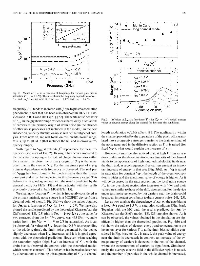
We shall now focus on , which is frequently considered asthe primary intrinsic noise source in a MOSFET device from acircuital point of view. In Fig. 3(a) we show the values obtainedfor as a function of for V. We have alsoplotted the results predicted by the theoretical Klaassen/van derZiel’s model [18], [23] (this is , the value for
, extracted from the – curve, was 435 S/m , andvaries from 1 for V to 2/3 in saturation). As it canbe observed, for values of lower than 0.5 V (correspondingto the triode regime), the drain noise generated by the deviceslightly decreases when increases, and it is in good agree-ment with the theoretical prediction. However, when reachingthe saturation region (high ) an increase of with thedrain bias is observed (in contrast with the theoretical model,which remains constant). This behavior has been also describedby other authors attributing this augmentation of to channel
Fig. 3. (a) Values ofS as a function ofV forV = 1:0V and (b) averagevalues of electron energy along the channel for the same bias conditions.
length modulation (CLM) effects [8]. The nonlinearity withinthe channel provoked by the appearance of the pinch off is trans-lated into a progressive stronger transfer to the drain terminal ofthe noise generated in the diffusive section as is raised (forfixed ), what would explain the increase of .
However, it must be also noticed that, at high in satura-tion conditions the above mentioned nonlinearity of the channelyields to the appearance of high longitudinal electric fields nearthe drain and, as a consequence, free carriers present an impor-tant increase of energy in that area [Fig. 3(b)]. As is raisedin saturation for constant , the length of the overshoot sec-tion is wider and the maximum value of energy is higher. As itwill be discussed in the next subsection, the local noise source
in the overshoot section also increases with and theirvalues are similar to those of the diffusive section. For the deviceunder test, noise generated by hot carriers near the drain couldbe also an important contributor to drain current noise [24], [25].
Let us now analyze the dependence of on the gate bias ata fixed equal to 1.5 V, in saturation conditions [Fig. 4(a)].Together with the MC data, the results predicted for byKlaassen/van der Ziel’s model [18], [23] are also shown. As itcan be observed, the values obtained in the simulation are sig-nificantly higher than the theoretical prediction. Fig. 4(b) and(c) shows the values of electron energy and concentration in theinversion layer for various at the drain bias condition con-sidered in Fig. 4(a). As is raised, the peak value of energynear the drain is decreased; in contrast, an increase of the av-erage energy of carriers is detected in the rest of the channel,where the concentration of carriers is significant. Simultane-ously, the average electric field in the diffusive region is raised,and the number of particles in the whole channel is increased.

526 IEEE TRANSACTIONS ON ELECTRON DEVICES, VOL. 53, NO. 3, MARCH 2006
Fig. 4. (a) Values ofS as a function ofV for a fixed drain bias, (b) averagevalues of energy, and (c) concentration of carriers along the channel for V =
1:5V and various gate-to-source voltages.
The combination of these facts produces an important augmen-tation of the local noise source within the channel, as it will beshown in the next subsection, thus producing the increase ofwith .
B. Velocity Fluctuation Noise
According to the procedure indicated in Appendix I, we ana-lyze the spectra of velocity fluctuations in the diffusive andovershoot sections of the channel, what can provide useful in-formation about the local current noise source. It is important toremark that we do no intend to “double calculate” by twoseparate methods: in fact, the determination of this quantity bymeans of the spectral density of velocity fluctuations would re-quire in a second step to evaluate the transfer of the local noisesource to the drain terminal through an impedance field [9]. Thecalculation of this impedance field by means of MC device sim-ulation is neither affordable nor reliable from the practical pointof view due to the stochastic nature of the simulation approach.
An example of velocity fluctuations (normalized to one par-ticle) in the diffusive and overshoot sections can be observed inFig. 5(a) and (b). As shown in the graph, the amplitude of fluc-tuations is much stronger in the overshoot section, what gives ahigher zero-time value of the correlation function of the velocityfluctuations. Fig. 5(c) shows the results for in Sections I andII as a function of for a fixed V. In the graph, we
Fig. 5. Velocity fluctuations as a function of time in (a) Section I and (b)Section II for V = 1:0V and V = 1:5V. (c) S as a function of Vfor fixed V = 1:5V; tendency lines are included (dotted lines). Dashed lineshows the value of S obtained from the bulk diffusion coefficient. Inset showsS as a function of V for V = 1:0V.
have also plotted, as a reference, the low-field value of ,being the diffusion coefficient calculated in bulk material withanalogous doping concentration as the substrate doping of theSOI structure. As it can be observed, the spectral intensity of ve-locity fluctuations, , is much stronger in Section II (velocityovershoot) than in Section I (diffusive) especially for low ,this is, in deep saturation and near the weak inversion regime.As is increased, the difference between both sections is re-duced: while in Section II does not show a significant depen-dence on , a progressive augmentation with the gate voltageis detected in Section I. This increase of in Section I is mainlydue to a larger zero-time value of the correlation function of ve-locity fluctuations (when is raised, the higher average lon-gitudinal electric field in that area yields to a larger amplitudeof velocity fluctuations), since the decay time of the correlationfunction does not vary significantly with . In the case ofSection II transport takes place under a quasi-ballistic regime,and once saturation conditions are reached for a given thevalues of are not substantially modified when varying .
It is noteworthy that, even in the case of Section I, in which thefeatures of transport are closer to a diffusive regime, the valuesobtained for are in general higher than the value predicted ifconsidering the bulk diffusion coefficient through . Inthis case, only for low (where the average energy of carriersis close to thermal equilibrium) a reasonable agreement is foundbetween both calculations.
The inset of Fig. 5(c) shows versus for the two sec-tions of the channel considered. For low , the device oper-

RENGEL et al.: MICROSCOPIC INTERPRETATION OF THE RF NOISE PERFORMANCE 527
Fig. 6. q NS as a function of gate biasing for V = 1:5V in the twosections of the channel considered. Inset shows the results for q NS as afunction of V for V = 1:0V.
ates in the triode regime, so the diffusive section in fact corre-sponds to the whole effective channel, where the device behavespractically like a linear resistor. At the beginning of saturation
V , is quite similar in both sections; neverthe-less, when is increased remains rather constant in Sec-tion I while it clearly augments in Section II. The increase of
at fixed leads (once that saturation is reached) to theappearance of nonstationary phenomena and elevated longitu-dinal electric fields near the drain. As a consequence, carriersin Section II progressively reach elevated energies [Fig. 3(b)]and the ballistic character of transport intensifies in that area.From this result, the increase of versus in saturation[Fig. 3(a)] could be attributed to a stronger contribution of thenoise generated in Section II. Nevertheless, it must be taken intoaccount also that as is raised the length of Section I is de-creased due to a stronger CLM effect: within the frameworkconsidered in this work a stronger impedance field in Section Iprovoked by CLM can not be discarded as the origin of currentexcess noise at the drain terminal.
To present a clearer idea of the local current noise sourcein each subsection of the channel, in Fig. 6 we have representedthe values of the NS factor [see (A1) in the Appendix]. Forboth sections, an increase of NS with is observed, whatexplains the augmentation of with the gate bias at fixedin saturation. In the case of Section II, the increase of NS isdue to the higher sheet carrier concentration as is raised,while in Section I the increase of both and [Fig. 5(c)] com-bine to produce a finally slightly higher NS factor than in theovershoot section. Checking the dependence on , shown inthe inset, it can be observed how Section I presents a strongervalue of NS , although at high (when carriers reach el-evated energies) the results for the overshoot section are quitesimilar to those for the diffusive region.
C. , and Parameters
Spectral densities provide very useful information for thehigh frequency noise analysis of the devices; nevertheless,if one wants to compare the intrinsic noise behavior of thedevice with other structures, it is necessary to use normalized
Fig. 7. Results for �, �, and C as a function of gate biasing.
parameters such as , which is related to drain noise, , asso-ciated to induced gate noise, and , related to the correlationbetween noise sources [18]. These parameters incorporate notonly the effect of intrinsic noise sources, but also the influenceof dynamic parameters, following the equations given in [26]and [27]:
(1)
(2)
(3)
where corresponds to the admittance parameters (1 and 2 cor-respond to the gate and to the drain terminals, respectively). Aspreviously mentioned, the dynamic behavior of the devices (an-alyzed through the calculation of parameters) was satisfac-torily evaluated in a previous work [14]. To complete the infor-mation concerning intrinsic noise sources, in Fig. 7 we show theresults for , and as a function of for V,in saturation conditions. First of all, an important increase ofwith the gate biasing is obtained as compared to van der Zielsprediction for a long channel device ( 0.7), which is due tothe enhancement of drain noise previously commented. On theother hand, it must be highlighted the increase of for highgate biasing, related to the corresponding raise of induced gatenoise because of the stronger capacitive coupling associated tothe elevated concentration of carriers along the channel. Re-garding the values of , their average value is around 0.35,slightly lower than the result predicted by long-channel FETtheory ( 0.4) [18].
D. Simulated and Experimental Extrinsic Noise Parameters
Once the intrinsic noise sources and parameters providedby the MC simulation have been exhaustively analyzed, wewill focus on the comparative study between experimentalmeasurements and simulation results. For this purpose, themost adequate parameters are the usual four noise parameters(NF , and complex ), together with the associatedgain that shall give more information to circuit designers.The process for calculating these parameters in the MC simula-tion is not an obvious task: the effect of extrinsic elements mustbe incorporated to the simulation results in order to allow a faircomparison with experimental data. For this purpose, we used
528 IEEE TRANSACTIONS ON ELECTRON DEVICES, VOL. 53, NO. 3, MARCH 2006
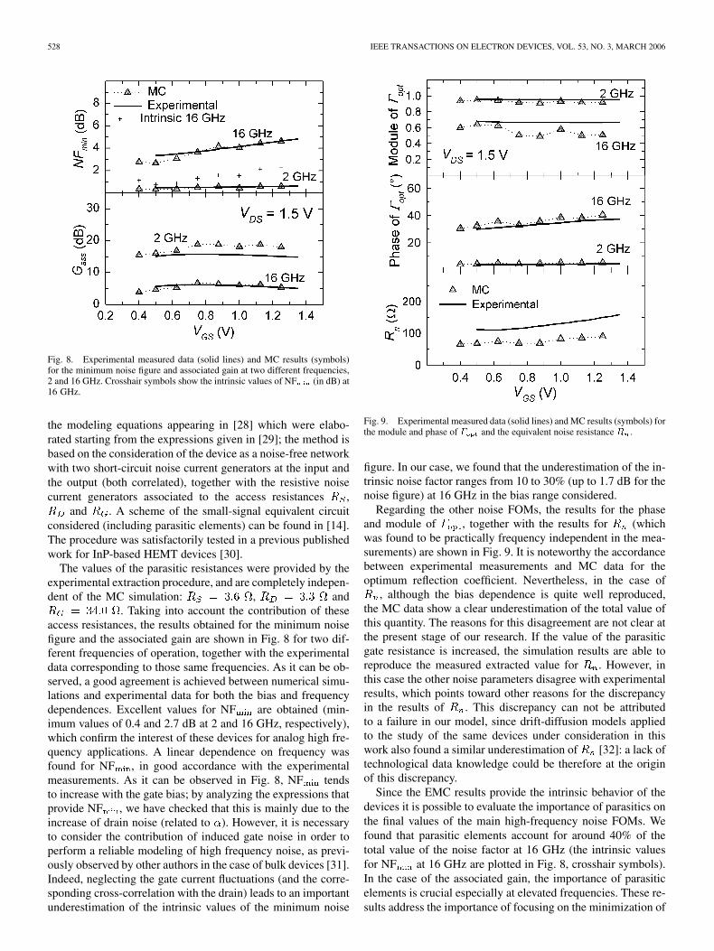
Fig. 8. Experimental measured data (solid lines) and MC results (symbols)for the minimum noise figure and associated gain at two different frequencies,2 and 16 GHz. Crosshair symbols show the intrinsic values of NF (in dB) at16 GHz.
the modeling equations appearing in [28] which were elabo-rated starting from the expressions given in [29]; the method isbased on the consideration of the device as a noise-free networkwith two short-circuit noise current generators at the input andthe output (both correlated), together with the resistive noisecurrent generators associated to the access resistances ,
and . A scheme of the small-signal equivalent circuitconsidered (including parasitic elements) can be found in [14].The procedure was satisfactorily tested in a previous publishedwork for InP-based HEMT devices [30].
The values of the parasitic resistances were provided by theexperimental extraction procedure, and are completely indepen-dent of the MC simulation: , and
. Taking into account the contribution of theseaccess resistances, the results obtained for the minimum noisefigure and the associated gain are shown in Fig. 8 for two dif-ferent frequencies of operation, together with the experimentaldata corresponding to those same frequencies. As it can be ob-served, a good agreement is achieved between numerical simu-lations and experimental data for both the bias and frequencydependences. Excellent values for NF are obtained (min-imum values of 0.4 and 2.7 dB at 2 and 16 GHz, respectively),which confirm the interest of these devices for analog high fre-quency applications. A linear dependence on frequency wasfound for NF , in good accordance with the experimentalmeasurements. As it can be observed in Fig. 8, NF tendsto increase with the gate bias; by analyzing the expressions thatprovide NF , we have checked that this is mainly due to theincrease of drain noise (related to ). However, it is necessaryto consider the contribution of induced gate noise in order toperform a reliable modeling of high frequency noise, as previ-ously observed by other authors in the case of bulk devices [31].Indeed, neglecting the gate current fluctuations (and the corre-sponding cross-correlation with the drain) leads to an importantunderestimation of the intrinsic values of the minimum noise
Fig. 9. Experimental measured data (solid lines) and MC results (symbols) forthe module and phase of � and the equivalent noise resistance R .
figure. In our case, we found that the underestimation of the in-trinsic noise factor ranges from 10 to 30% (up to 1.7 dB for thenoise figure) at 16 GHz in the bias range considered.
Regarding the other noise FOMs, the results for the phaseand module of , together with the results for (whichwas found to be practically frequency independent in the mea-surements) are shown in Fig. 9. It is noteworthy the accordancebetween experimental measurements and MC data for theoptimum reflection coefficient. Nevertheless, in the case of
, although the bias dependence is quite well reproduced,the MC data show a clear underestimation of the total value ofthis quantity. The reasons for this disagreement are not clear atthe present stage of our research. If the value of the parasiticgate resistance is increased, the simulation results are able toreproduce the measured extracted value for . However, inthis case the other noise parameters disagree with experimentalresults, which points toward other reasons for the discrepancyin the results of . This discrepancy can not be attributedto a failure in our model, since drift-diffusion models appliedto the study of the same devices under consideration in thiswork also found a similar underestimation of [32]: a lack oftechnological data knowledge could be therefore at the originof this discrepancy.
Since the EMC results provide the intrinsic behavior of thedevices it is possible to evaluate the importance of parasitics onthe final values of the main high-frequency noise FOMs. Wefound that parasitic elements account for around 40% of thetotal value of the noise factor at 16 GHz (the intrinsic valuesfor NF at 16 GHz are plotted in Fig. 8, crosshair symbols).In the case of the associated gain, the importance of parasiticelements is crucial especially at elevated frequencies. These re-sults address the importance of focusing on the minimization of
RENGEL et al.: MICROSCOPIC INTERPRETATION OF THE RF NOISE PERFORMANCE 529
parasitic elements in order to fully profit from the exceptionalintrinsic behavior of the device under test. Moreover, taking intoaccount that parasitics can be reasonably predicted for a giventechnology when performing the downscaling, the simulator canbe of great help to predict the tendency for the high-frequencynoise behavior of future downscaled devices.
IV. CONCLUSION
A complete numerical and experimental investigation of thehigh-frequency noise behavior of deep-submicrometer FD SOIMOSFETs has been performed in this work. The informationprovided by the simulator, in terms of the internal quantities ofinterest, allows getting a proper understanding of the intrinsicnoise sources. The bias dependence of the spectral density fordrain current fluctuations has been deeply analyzed, paying at-tention to the onset of excess noise and the appearance of hotcarriers. The study of local velocity fluctuations by means of theensemble MC simulation has shown that carriers in the velocityovershoot region have a stronger intensity of velocity fluctua-tions and produce a significant local noise source. However, afinal conclusion about its influence on the drain current noisewould require the reliable evaluation of the adequate transferfield by means of deterministic approaches. The results have ev-idenced that in the case of the diffusive section, only for lowa reasonable agreement is found between and the predictionobtained by considering the diffusion coefficient correspondingto bulk material.
The detailed consideration of the real topology of the devicesand the parasitic elements yields a general good agreement be-tween the experimental measurements and the MC simulationfor the most relevant noise FOMs, which confirms the reliabilityof the simulator for the study of high-frequency noise. It mustalso be mentioned the importance of a correct determination ofinduced gate noise in order to perform a reliable calculation ofthe minimum noise figure. Although the devices show an excel-lent behavior in the GHz frequency range of operation in termsof NF and , we have found that parasitic elements playa determinant role on the total noise generated by the device.In particular, the influence of parasitics on the minimum noisefigure can be weighted of around 40% of the total value of thenoise factor at 16 GHz, which may mask the excellent intrinsicperformance of the device.
APPENDIX I
Most of the deterministic approaches for the study of noiseare based in the consideration of ad hoc local current noisesources which are weighted by appropriate transfer fields (thatcan be determined i.e., by using Green functions) to obtaintheir contribution to the final current/voltage noise at theterminals, as in the so-called impedance field method (IFM).Within this framework, the local current noise source can beexpressed in terms of the noise spectrum of the local velocityfluctuations [33]
(A1)
where is the electron charge, the local sheet carrier den-sity, is the length of the local section, the device width,
the local noise source and the local noisespectrum of velocity fluctuations, also know as velocity-fluctu-ation noise [18]
(A2)
where corresponding to velocity fluctuation correspondingto one particle. According to Kubo [34], is related to thehigh-frequency diffusion constant through
, so in most cases the diffusion coefficient substi-tutes in the definition of the local noise source.1
To determine the noise spectrum of current fluctuations at thedrain terminal, it is necessary to take into account the influenceof a transfer field
(A3)
where is a dimensionless factor that, by analogy to theIFM method applied to the calculation of voltage noise, is usu-ally known as the “impedance field” [9].
In our model (A.3) is not employed since orare not necessary to determine the final current noise
, which is directly obtained from the MC values of theinstantaneous current fluctuations at the terminals (see Sec-tion II). However, we may evaluate both andin two different regions of the channel in order to examinethe values of the local current noise source (which can be ofgreat interest for other groups using deterministic approaches)since in our model velocity fluctuations are naturally givenwithout making any assumption about their origin, and hotcarrier phenomena are “built-in” in the simulation. For thispurpose, we have developed a procedure to determine, bymeans of the data provided by the EMC simulator, the valueof , a quantity frequently used as the primary noisesource in deterministic approaches. Special care was given tofulfill the requirements to correctly determine this noise source[36], [37]: the contribution of concentration fluctuations mustbe eliminated and the calculation must be performed in theabsence of fluctuations of the self-consistent electric field. Forthis latter purpose, we “froze” the electric field by consideringits average value after a preliminary simulation during 100 ps.
Let us consider a section of the channel. Since the EMCsimulation provides the instantaneous values of velocity foreach simulated particle, we add all the values of longitudinalvelocity (which is the velocity component that contributes todc current and low frequency noise) of particles present ineach section of the channel. The total sum is divided by theinstantaneous number of particles present in that sectionin order to obtain the average instantaneous velocity
(A4)
1To properly investigate nonequilibrium conditions or hot carrier phenomena,a possibility is to extend the use of the Einstein relation with the adequate con-sideration of the noise temperature and the mobility; this issue still remains acontroversial question, yielding different solutions in the literature (i.e., [32],[35]).
530 IEEE TRANSACTIONS ON ELECTRON DEVICES, VOL. 53, NO. 3, MARCH 2006
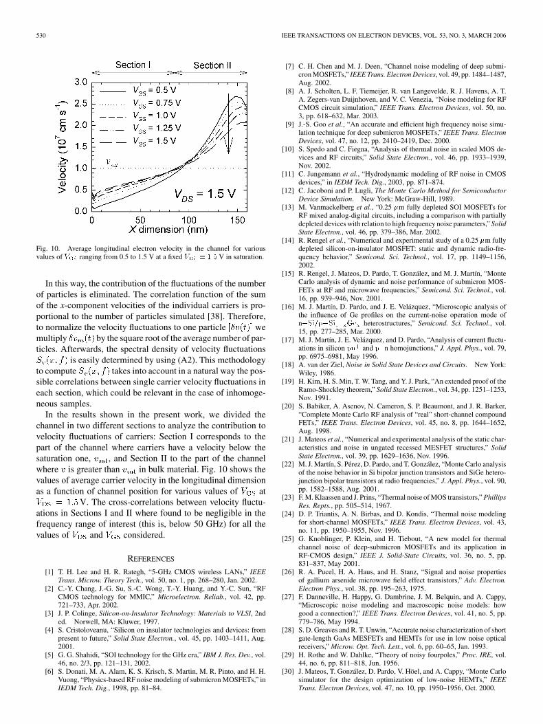
Fig. 10. Average longitudinal electron velocity in the channel for variousvalues of V ranging from 0.5 to 1.5 V at a fixed V = 1:5V in saturation.
In this way, the contribution of the fluctuations of the numberof particles is eliminated. The correlation function of the sumof the x-component velocities of the individual carriers is pro-portional to the number of particles simulated [38]. Therefore,to normalize the velocity fluctuations to one particle wemultiply by the square root of the average number of par-ticles. Afterwards, the spectral density of velocity fluctuations
is easily determined by using (A2). This methodologyto compute takes into account in a natural way the pos-sible correlations between single carrier velocity fluctuations ineach section, which could be relevant in the case of inhomoge-neous samples.
In the results shown in the present work, we divided thechannel in two different sections to analyze the contribution tovelocity fluctuations of carriers: Section I corresponds to thepart of the channel where carriers have a velocity below thesaturation one, , and Section II to the part of the channelwhere is greater than in bulk material. Fig. 10 shows thevalues of average carrier velocity in the longitudinal dimensionas a function of channel position for various values of at
V. The cross-correlations between velocity fluctu-ations in Sections I and II where found to be negligible in thefrequency range of interest (this is, below 50 GHz) for all thevalues of and considered.
REFERENCES
[1] T. H. Lee and H. R. Rategh, “5-GHz CMOS wireless LANs,” IEEETrans. Microw. Theory Tech., vol. 50, no. 1, pp. 268–280, Jan. 2002.
[2] C.-Y. Chang, J.-G. Su, S.-C. Wong, T.-Y. Huang, and Y.-C. Sun, “RFCMOS technology for MMIC,” Microelectron. Reliab., vol. 42, pp.721–733, Apr. 2002.
[3] J. P. Colinge, Silicon-on-Insulator Technology: Materials to VLSI, 2nded. Norwell, MA: Kluwer, 1997.
[4] S. Cristoloveanu, “Silicon on insulator technologies and devices: frompresent to future,” Solid State Electron., vol. 45, pp. 1403–1411, Aug.2001.
[5] G. G. Shahidi, “SOI technology for the GHz era,” IBM J. Res. Dev., vol.46, no. 2/3, pp. 121–131, 2002.
[6] S. Donati, M. A. Alam, K. S. Krisch, S. Martin, M. R. Pinto, and H. H.Vuong, “Physics-based RF noise modeling of submicron MOSFETs,” inIEDM Tech. Dig., 1998, pp. 81–84.
[7] C. H. Chen and M. J. Deen, “Channel noise modeling of deep submi-cron MOSFETs,” IEEE Trans. Electron Devices, vol. 49, pp. 1484–1487,Aug. 2002.
[8] A. J. Scholten, L. F. Tiemeijer, R. van Langevelde, R. J. Havens, A. T.A. Zegers-van Duijnhoven, and V. C. Venezia, “Noise modeling for RFCMOS circuit simulation,” IEEE Trans. Electron Devices, vol. 50, no.3, pp. 618–632, Mar. 2003.
[9] J.-S. Goo et al., “An accurate and efficient high frequency noise simu-lation technique for deep submicron MOSFETs,” IEEE Trans. ElectronDevices, vol. 47, no. 12, pp. 2410–2419, Dec. 2000.
[10] S. Spedo and C. Fiegna, “Analysis of thermal noise in scaled MOS de-vices and RF circuits,” Solid State Electron., vol. 46, pp. 1933–1939,Nov. 2002.
[11] C. Jungemann et al., “Hydrodynamic modeling of RF noise in CMOSdevices,” in IEDM Tech. Dig., 2003, pp. 871–874.
[12] C. Jacoboni and P. Lugli, The Monte Carlo Method for SemiconductorDevice Simulation. New York: McGraw-Hill, 1989.
[13] M. Vanmackelberg et al., “0.25 �m fully depleted SOI MOSFETs forRF mixed analog-digital circuits, including a comparison with partiallydepleted devices with relation to high frequency noise parameters,” SolidState Electron., vol. 46, pp. 379–386, Mar. 2002.
[14] R. Rengel et al., “Numerical and experimental study of a 0.25 �m fullydepleted silicon-on-insulator MOSFET: static and dynamic radio-fre-quency behavior,” Semicond. Sci. Technol., vol. 17, pp. 1149–1156,2002.
[15] R. Rengel, J. Mateos, D. Pardo, T. González, and M. J. Martín, “MonteCarlo analysis of dynamic and noise performance of submicron MOS-FETs at RF and microwave frequencies,” Semicond. Sci. Technol., vol.16, pp. 939–946, Nov. 2001.
[16] M. J. Martín, D. Pardo, and J. E. Velázquez, “Microscopic analysis ofthe influence of Ge profiles on the current-noise operation mode ofn�Si=p�Si Ge heterostructures,” Semicond. Sci. Technol., vol.15, pp. 277–285, Mar. 2000.
[17] M. J. Martín, J. E. Velázquez, and D. Pardo, “Analysis of current fluctu-ations in silicon pn and p n homojunctions,” J. Appl. Phys., vol. 79,pp. 6975–6981, May 1996.
[18] A. van der Ziel, Noise in Solid State Devices and Circuits. New York:Wiley, 1986.
[19] H. Kim, H. S. Min, T. W. Tang, and Y. J. Park, “An extended proof of theRamo-Shockley theorem,” Solid State Electron., vol. 34, pp. 1251–1253,Nov. 1991.
[20] S. Babiker, A. Asenov, N. Cameron, S. P. Beaumont, and J. R. Barker,“Complete Monte Carlo RF analysis of “real” short-channel compoundFETs,” IEEE Trans. Electron Devices, vol. 45, no. 8, pp. 1644–1652,Aug. 1998.
[21] J. Mateos et al., “Numerical and experimental analysis of the static char-acteristics and noise in ungated recessed MESFET structures,” SolidState Electron., vol. 39, pp. 1629–1636, Nov. 1996.
[22] M. J. Martín, S. Pérez, D. Pardo, and T. González, “Monte Carlo analysisof the noise behavior in Si bipolar junction transistors and SiGe hetero-junction bipolar transistors at radio frequencies,” J. Appl. Phys., vol. 90,pp. 1582–1588, Aug. 2001.
[23] F. M. Klaassen and J. Prins, “Thermal noise of MOS transistors,” PhillipsRes. Repts., pp. 505–514, 1967.
[24] D. P. Triantis, A. N. Birbas, and D. Kondis, “Thermal noise modelingfor short-channel MOSFETs,” IEEE Trans. Electron Devices, vol. 43,no. 11, pp. 1950–1955, Nov. 1996.
[25] G. Knoblinger, P. Klein, and H. Tiebout, “A new model for thermalchannel noise of deep-submicron MOSFETs and its application inRF-CMOS design,” IEEE J. Solid-State Circuits, vol. 36, no. 5, pp.831–837, May 2001.
[26] R. A. Pucel, H. A. Haus, and H. Stanz, “Signal and noise propertiesof gallium arsenide microwave field effect transistors,” Adv. Electron.Electron Phys., vol. 38, pp. 195–263, 1975.
[27] F. Danneville, H. Happy, G. Dambrine, J. M. Belquin, and A. Cappy,“Microscopic noise modeling and macroscopic noise models: howgood a connection?,” IEEE Trans. Electron Devices, vol. 41, no. 5, pp.779–786, May 1994.
[28] S. D. Greaves and R. T. Unwin, “Accurate noise characterization of shortgate-length GaAs MESFETs and HEMTs for use in low noise opticalreceivers,” Microw. Opt. Tech. Lett., vol. 6, pp. 60–65, Jan. 1993.
[29] H. Rothe and W. Dahlke, “Theory of noisy fourpoles,” Proc. IRE, vol.44, no. 6, pp. 811–818, Jun. 1956.
[30] J. Mateos, T. González, D. Pardo, V. Höel, and A. Cappy, “Monte Carlosimulator for the design optimization of low-noise HEMTs,” IEEETrans. Electron Devices, vol. 47, no. 10, pp. 1950–1956, Oct. 2000.

RENGEL et al.: MICROSCOPIC INTERPRETATION OF THE RF NOISE PERFORMANCE 531
[31] D. K. Shaeffer and T. H. Lee, “A 1.5-V, 1.5-GHz CMOS low noise am-plifier,” IEEE J. Solid-State Circuits, vol. 32, no. 5, pp. 745–759, May1997.
[32] G. Pailloncy, B. Iñiguez, G. Dambrine, J.-P. Raskin, and F. Danneville,“Noise modeling in fully depleted SOI MOSFETs,” Solid State Elec-tron., vol. 48, pp. 813–825, May 2004.
[33] A. Cappy and W. Heinrich, “High-frequency FET noise performance:a new approach,” IEEE Trans. Electron Devices, vol. 36, no. 2, pp.403–409, Feb. 1989.
[34] R. Kubo, “Statistical-mechanical theory of irreversible processes. I.General theory and simple applications to magnetic and conductionproblems,” J. Phys. Soc. Japan, vol. 12, pp. 570–586, Jun. 1957.
[35] K. Han, H. Shin, and K. Lee, “Analytical drain thermal noise currentmodel valid for deep submicron MOSFETs,” IEEE Trans. Electron De-vices, vol. 51, no. 2, pp. 261–269, Feb. 2004.
[36] P. Shiktorov et al., “Transfer-field methods for electronic noise in sub-micron semiconductor structures,” Rivista Nuovo Cimento, vol. 24, pp.1–71, 2001.
[37] , “On the spectral strength of the noise source entering the transferimpedance method,” Appl. Phys. Lett., vol. 71, pp. 3093–3095, Nov.1997.
[38] J. Zimmermann and E. Constant, “Application of Monte Carlo tech-niques to hot carrier diffusion noise calculation in unipolar semicon-ducting components,” Solid State Electron., vol. 23, pp. 915–925, 1980.
Raúl Rengel was born in Tarrasa, Spain, in 1974. Hereceived the B.S. and Ph.D. degrees in physics fromthe University of Salamanca, Salamanca, Spain, in1997 and 2003, respectively.
From 1998 to 2000, he was with the ElectronicsGroup, Department of Applied Physics, Universityof Salamanca as a Grant Holder. In 2001, he be-came Assistant Professor. He was a PostdoctoralResearcher during his six months at the Instituted’Electronique, de Microélectronique et de Nan-otechnologies (IEMN), Villeneuve d’Ascq, Cedex,
France. His main research activity is the MC modeling of electron transport insilicon devices, including the investigation of electronic noise processes andsmall-signal behavior in the high frequencies range in SOI MOSFET transistorsand nonconventional silicon devices.
María Jesús Martín was born in Salamanca, Spain,in 1969. She received the B.S. and Ph.D. degreesin physics from the University of Salamanca, Sala-manca, Spain, in 1992 and 1996, respectively.
Since 1992 she has been with the ElectronicsGroup, Department of Applied Physics,Universityof Salamanca as a Grant Holder. Her graduate workfocused on the simulation of transport and electronicnoise in bipolar Si and SiGe structures. In 1995, shebecame Assistant Professor. She worked in 1997and 1998 at the Electronic Components Technology
and Materials (ECTM), Technological University of Delft, Delft, The Nether-lands. This collaboration was in the field of designing MMIC amplifiers, foruse in front-ends for GSM and DECT applications (using TEMIC’s silicongermanium SiGe1 process). In 2002, she became Associate Professor ofthe University of Salamanca. Her current research interest is in the field ofmodeling of electronic transport and noise of submicrometer silicon devices.
Tomás González (M’05) was born in Salamanca,Spain, in 1967. He graduated in physics from theUniversity of Salamanca, Salamanca, Spain, in 1990,where he received the Ph.D. degree in physics in1994.
Since 1991 he has been working with the Elec-tronics Group, Department of Applied Physics,University of Salamanca, with a Grant from theSpanish Education Ministry. In 1996 he becameAssociate Professor. His main research activity isin the field of electronic transport in semiconductor
materials, electronic devices and mesoscopic structures, with special applica-tion to the modeling of electronic noise by microscopic approaches.
Javier Mateos was born in Salamanca, Spain, in1970. He received the B.S. and Ph.D. degrees inphysics from the University of Salamanca in 1993and 1997, respectively.
Since 1993 he has been with the ElectronicsGroup, Department of Applied Physics, Univer-sity of Salamanca, as a Grant Holder. In 1996,he became Assistant Professor. He was with theInstitut d’Electronique, de Microélectronique et deNanotechnologies (IEMN), Lille, France for a year,where, in 2000, he became an Associate Professor.
His present research interest is in the development of novel device conceptsusing ballistic transport, together with the modeling and optimization of thehigh-frequency and low-noise performance of ultrashort gate-length HEMTs.
Daniel Pardo was born in Valladolid, Spain, in1946. He received the degree and the Ph.D. degreein physics from the University of Valladolid in 1971and 1975, respectively.
From 1971 to 1981, he was with the ElectronicsDepartment, University of Valladolid, working onthe characterization of semiconductor materials andmodeling of semiconductor devices. He becameAssociate Professor in 1978. In 1981, he joinedthe Applied Physics Department, University ofSalamanca, Salamanca, Spain, where he became a
Full Professor and Head of the Electronics Group in 1983. His current researchinterest is the Monte Carlo simulation of semiconductor devices with specialapplication to noise modeling.
Gilles Dambrine (M’92) was born in Avion, France,on May 15, 1959. In 1986, he joined the CentreHyperfréquences et Semiconducteurs, Universityof Lille, Lille, France, where he received the Ph.D.degree and the Habilitation à Diriger des Recherches(HDR) en Sciences degree in 1989 and 1996,respectively.
He was a Full Researcher at the Centre Nationalde Recherche Scientifique (CNRS), France, between1989 and 1999. He is now Professor of Electronics,University of Lille. His main research interests
are concerned with the modeling and characterization of ultimate low-noisedevices for application in millimeter- and sub-millimeterwave ranges. Heis now the head of the “Advanced Nanometric Devices” (ANODE) groupat Institut d’Electronique, de Microélectronique et de Nanotechnologie,”Villeneuve d’Ascq, France. His research interests are oriented to the study ofthe microwave and millimeter-wave properties and applications of advancedsilicon devices. He is author or coauthor of about 30 papers and 40 internationalcommunications and four book chapters in the field of microwave devices.
Prof. Dambrine is a member of the Technical Program Committee of the IEEEInternational Microwave Symposium and the European Microwave Conferencesince 2000. He is currently a reviewer in various IEEE TRANSACTIONS.

532 IEEE TRANSACTIONS ON ELECTRON DEVICES, VOL. 53, NO. 3, MARCH 2006
Jean-Pierre Raskin (M’97) was born in Aye,Belgium, in 1971. He received the Industrial Engi-neer degree from the Institut Supé;rieur Industrield’Arlon, Belgium, in 1993, and the B.S. and Ph.D.degrees in applied sciences from the UniversitéCatholique de Louvain (UCL), Louvain-la-Neuve,Belgium, in 1994 and 1997, respectively.
From 1994 to 1997, he was a Research Engineerat the Microwave Laboratory, UCL. He workedon the modeling, characterization, and realizationof MMICs in SOI technology for low-power,
low-voltage applications. In 1998, he joined the Electrical Engineering andComputer Science Department, The University of Michigan, Ann Arbor. Hehas been involved in the development and characterization of micromachiningfabrication techniques for microwave and millimeter-wave circuits and mi-croelectromechanical transducers/amplifiers working in hard environments.Since Jan. 2000, he is an Associate Professor at the Microwave Laboratory,UCL. His research interests are the modeling, wide-band characterization, andfabrication of advanced SOI MOSFETs as well as micro and nanofabrication ofMEMS/NEMS sensors and actuators. He is a member of the Research Centerin Micro and Nanoscopic Materials and Electronic Devices of the UCL. He isthe author or coauthor of more than 200 scientific articles.
Dr. Raskin is an EuMA Associate Member.
François Danneville (M’98) was born in Ham,France, on March 16, 1964. He received the Ph.D.degree from the the Habilitation à Diriger desRecherches (HDR) and the Sciences degree fromthe Centre Hyperfréquences et Semiconducteurs,University of Lille, Lille, France, in 1991 and 1999,respectively.
In 1991, he was an Associate Professor, Univer-sity of Lille, and his research has been carried outat the Institut d’Electronique, de Microélectroniqueet de Nanotechnologie (IEMN), Villeneuve d’Ascq,
France, where he has studied the noise properties of III-V devices operating inlinear and nonlinear regimes, for applications in centrimetric and millimetricranges. In 1998, he held was a Visiting Professor in noise expertise at Hewlett-Packard (now Agilent), Electrical Engineering Division, Santa Rosa, CA. Since2001, he is a Full Professor, University of Lille where his research at IEMNis oriented toward the study of the dynamic, noise, and nonlinear properties ofMOSFET-based devices (including alternative architectures) and SiGe HBT aswell as the design of low noise/low power circuits in millimetric wave rangeusing SOI and SiGe BiCMOS technologies. He has authored or co-authoredabout 80 scientific international publications and communications. Heis an Ed-itor for Fluctuation and Noise Letters.
Dr. Danneville has been Chairman of the Microwave Low Noise andTechniques Conference, the MTT-14 Technical Committee, and the IEEEMicrowave Theory and Techniques Conference. He has been a member ofseveral International Scientific or TP Committees (UPoN ’99, SPIE FaN 2003,ICNF 2003 and 2005, and ICCDCS 2004). He was also the Chairman ofthe Noise in Devices and Circuits Conference, SPIE Fluctuations and NoiseSymposium 2004, Maspalomas and Co-Chairman of the last Noise in Devicesand Circuits Conference, which was part of the SPIE Fluctuations and noiseSymposium held in Austin, TX.


![Microscopic and macroscopic creativity [Comment]](https://static.fdokumen.com/doc/165x107/63222cba63847156ac067f99/microscopic-and-macroscopic-creativity-comment.jpg)