Electron microscopic study of the liver with biliary atresia and neonatal hepatitis
Upload
khangminh22Category
view
0download
0
Transmission Electron Microscopic Investigation of Transmission Electron Microscopic Investigation of Intergranular Glassy FilmsIntergranular Glassy Films
ANANDH SUBRAMANIAMDepartment of Applied Mechanics
INDIAN INSTITUTE OF TECHNOLOGY DELHINew Delhi-
110016Ph: (+91) (11) 2659 1340, Fax: (+91) (11) 2658 1119
[email protected], [email protected]://web.iitd.ac.in/~anandh
http://web.iitd.ac.in/~anandh/downloads/IGF.ppt
August 2007
This talk is dedicated to the fond memory of
Prof. Rowland M Cannon 1943-2006
Last at Lawrence Berkeley National Laboratory
University of California, Berkeley

OVERVIEW OF INTERGRANULAR GLASSY FILMS (OVERVIEW OF INTERGRANULAR GLASSY FILMS (IGFsIGFs))
SystemsSystems
Formation of an Formation of an IGFIGF
Effect of Various StimuliEffect of Various Stimuli
Theoretical & Computational MethodsTheoretical & Computational Methods
EXPERIMENTAL METHODS TO STUDY THE STRUCTUREEXPERIMENTAL METHODS TO STUDY THE STRUCTURE
TRANSMISSION ELECTRON MICROSCOPY (TEM)TRANSMISSION ELECTRON MICROSCOPY (TEM)
Diffuse Dark Field Imaging Diffuse Dark Field Imaging
High Resolution Electron Microscopy High Resolution Electron Microscopy
FresnelFresnel
Fringe ImagingFringe Imaging
OUTSTANDING ISSUESOUTSTANDING ISSUES
FINITE ELEMENT ANALYSIS AT THE NANOSCALEFINITE ELEMENT ANALYSIS AT THE NANOSCALE
OUTLINEOUTLINE
Keywords: Intergranular glassy film, amorphous structure, equilibrium thickness,
partial ordering, diffuse interface, Transmission Electron Microscopy.
Development of new techniques

INTERFACES
Based on misorientationof the bounding grains
Base
d on
che
mis
try
Base
d on
ord
er
Based on phase of the bounding grains Pure
With segregation
Ordered
Disordered
Special Random
Homophase Heterophase
Low angle CSL
Monolayer Multilayer
Possible ways of looking at internal interfaces in materials. The descriptions that fit Intergranular Glassy Films have been shaded.
[1] "Intergranular glassy films: an overview" Anandh Subramaniam, C.T. Koch and M. Rühle, Materials Science and Engineering A, 422 (2006) 3-18.
[1]
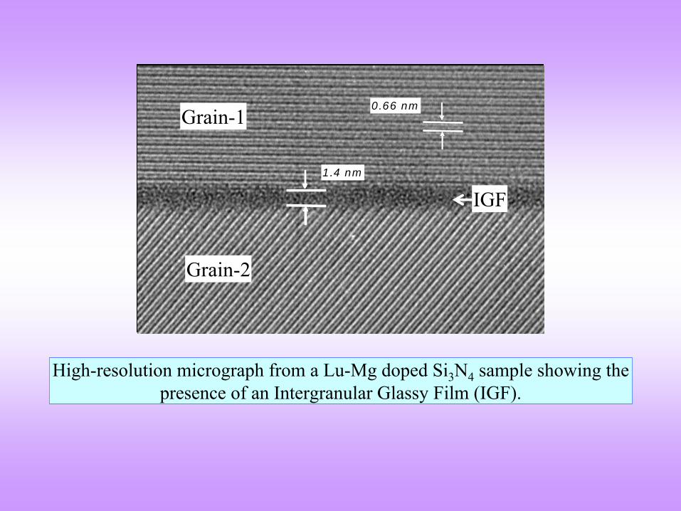
0.66 nm
1.4 nm
IGF
Grain-1
Grain-2
0.66 nm
1.4 nm
IGF
Grain-1
Grain-2
High-resolution micrograph from a Lu-Mg doped Si3
N4
sample showing the presence of an Intergranular Glassy Film (IGF).

IGF
Nearly constant thickness
Basically independent of the orientation of the bounding grains
Amorphous grain boundary film ~1-2 nm thick
Dependent on the composition of the ceramic
Independent of amount of glass excess glass goes to n-pocket
Resistant to crystallization
Composition and atomic structure different from the bulk glass
Basics

Systems in which IGFs
form
Ceramic-ceramic interface:
Si3
N4
(Undoped and doped with MgO, Y2 O3 , Rare Earth oxides, CaO, F, Cl)
SiC
Al2
O3
SrTiO3
ZnO
(Bi2
O3
doped)
Si2
N2
O
SiAlON
TiO2
-SiO2
Mullite
Ceramic-ceramic heterointerface
in composites:
Ruthenate
(Ru2 O, Pb2 Ru2 O7 , Bi2 Ru2 O7 ) - silicate glass (PbO-Al2 O3 - TiO2 -
SiO2 ) composites
Si3
N4
-SiC
Metal-ceramic interface:
Al2
O3
-Cu
Al2
O3
-Ni
Si3
N4
-Al.
In addition to the grain boundaries IGFs
are also found between the crystallized triple pocket phase and the grains in Si3
N4
and SiC.
Amorphous surface films
also show equilibrium thickness:
Si1-x
Zrx
O2
films on Si
Bi2
O3
films on ZnO
Epitaxial crystallization(ABC-SiC, 1100ºC, 500h)
Desegregation(Bi2O3 doped ZnO, 700ºC, 1 GPa, 2 h)
Thinning of IGF()
Stable films with altered thickness & wide films
(Si3N4 + MgO, quenched from 1350-1650ºC)
Pressure
Provides a weak path for intergranular fracture
Bimodal film size distribution(Si3N4 + Y2O3, 1430ºC, 40 MPa, 690 h)
Thinning of IGF(Si3N4 + Yb2O3 + Al2O3, 1400ºC, 168 h, air)
FractureCreep
Oxidation
Hea
ting
Liquid phase sinteringSi3N4, SiC, Al2O3, SrTiO3
Solid state activated sinteringBi2O3 doped ZnO
Crystallization of glassSiO2-TiO2
(+ quenching)
(annealing)
Principal methods of IGF formation Effect of various stimuli and treatments on IGF
Surface films:Heating 700ºC, 780ºCBi2O3 doped ZnO powders
Surface films:Heating 700ºC, PO2<10-50atm
Si1-xZrxO2 films on Si
IGF
Principal methods for the formation of IGF
& effect of various stimuli

Properties influenced by the structure of
the IGF
Fracture toughness
Oxidation resistance
Creep resistance
Electrical properties (ZnO, SrTiO3 )

Effect of composition of the ceramic
IGF
thickness in Si3
N4
Ca Content
Addition of
Oxides
C.M. Wang, X. Pan, M.J. Hoffmann, R.M. Cannon, M. Rühle, J. Am. Ceram. Soc. 79 (1996) 788-92.
I. Tanaka, H.-J. Kleebe, M.K. Cinibulk, J. Bruley, D.R. Clarke, M.Rühle, J. Am. Ceram. Soc. 77 (1994) 911-14.

Crystal-1
Crystal-2
PocketIGF
Graded ‘equilibrium’ IGF
Transition regionfrom PocketIGF to
Bulk
IGF-POCKET CONFIGURATIONS
TP-IGF
region
Segregation of Ca
IGF-2Crystal-1
Crystal-2
IGF-1t1
t2
Different CrystalStructure
Liquid-1
Liquid-2
IGF
Heterophase
IGF
Phase separation of glass in the pocket

Theoretical and computational methods to understand IGFs
Disordered GB
Seggregation
Phase separation
Force Balance
Wetting/Adsorbtion
Phase Field Model
Diffuse Interface Model
Near wetting precursor model
IGF
Ab-initiomethods
Molecular Dynamics/ Monte Carlo
Ways of looking at IGFs Atomistic simulation Methods Continuum theoretical Models

Understanding IGF
as an multilayer segregation
‘Glassy’ region having finite thickness
Progressive addition of a species preferentially segregating to a grain boundary
Monolayer Multilayer

DispersionForces
StearicForces
Space ChargeForces
Repulsive
Attractive
Attractive orRepulsive
Force balance model for equilibrium thickness of IGFs
Schematic of two possible energy-
displacement curves leading to equilibrium thickness of film
Clarke’s model: Forces leading to equilibrium
(a)
(b)
Minima
Minimum at zero displacement
DisplacementEn
ergy
Curves (a) and (b) are displaced verticallyfor visibility
Ackler
and Chiang’s model
Clarke’s model
Clarke’s model:•
Repulsive forces balance the attractive forces to give an equilibrium thickness for the film.•
Orientation effects of the grains are ignored in the model.•
Dry boundaries are explained in terms of an interfacial energy criterion

GB (Clean)
SL
GB (a = a*)
Dry boundaries
Cusps corresponding to special boundaries
Sum of the two crystal-glass interfacial energies
Grain misorientation
Inte
rfac
ial E
nerg
y
Explanation of dry boundaries based on interface energy versus misorientation plot. The hatched dry boundaries are based on GB (clean).
The GB (a = a*) corresponds to the GB energy with adsorbate coverage at an equilibrium concentration, appropriate to the two phase co-existence condition
Dry Boundaries
In materials like
Si3
N4
it is observed
that not all boundaries
have an IGF
i.e. some boundaries
are dry

Experimental methods to understand IGFs
Experimental methods
Scanning Electron Microscopy (SEM)
Auger Electron Spectroscopy
Transmission Electron Microscopy (TEM)
Impedance Spectroscopy
Mechanical Spectroscopy
Thickness & Structure of IGFs
by
Transmission Electron Microscopy
High-resolutionLattice fringe imaging
Fresnel
fringe techniquesDiffuse dark field imaging
Diffraction analysis Electron holography
High-angle annular dark field imaging
Energy dispersive X-ray analysis
Electron energy loss spectroscopy
"Aspects regarding measurement of thickness of Intergranular Glassy Films"
S. Bhattacharyya, Anandh Subramaniam,
C.T. Koch and M. Rühle
Journal of Microscopy, 221, p. 46, 2006.

Important Advances
Technology of microscopes:
(i) Spherical aberration correctors for illumination as well as imaging lens systems, (ii) Electron beam monochromators
reducing the energy spread of the electron beam
to <0.1eV, (iii) High-energy resolution spectrometers, (iv) Imaging energy filters, (v) Advanced specimen holders for in-situ experiments, (vi) High-sensitivity and high-dynamic-range detectors for images, diffraction
patterns, electron energy loss spectra (EELS), and energy
dispersive X-ray
spectra (EDXS).
New methods, such as focal series reconstruction has added to its utility. Thus, it has
become possible to record phase contrast images with point resolutions of well below
0.1nm, or alternatively, scan electron probes of size <0.1nm
across the specimen,
recording high-angle scattering or high-energy-resolution spectra from areas as small
as a single atomic column.

In some materials (e.g. stoichiometric
SrTiO3
), the frequency of GBs
with an
IGF
is very small.
In samples with large grain-size (~tens of microns), this problem is even more
severe
The grain boundaries in stoichiometric
SrTiO3
are usually not planar and only a
portion of the GB can be made approximately edge-on. This implies that tilt
along an axis perpendicular to the GB (i.e., keeping boundary
edge-on) is severely limited.
Sample and Microscope imposed constraints in HREM
of IGFs
Material related
Microscope related
Related to resolution and available tilt angles.
For SrTiO3
only five planes fall into the resolution range of a standard
microscope like JEOL
4000EX [(001), (101), (111), (002) and (102)].
In this microscope, with a top entry holder, tilt available is 10º
and sharp lattice
fringe contrast sometimes cannot be obtained on both sides of
the IGF
within this
tilt regime.

Direction of the electon beam
Two planes in the path of the electon beam with differing order at the GB
Direction of the electon beam
True disorder versus other cases (as seen in TEM)
True disorder at the boundary
Formation of an IGF
Roughening at the GB
Strain at the grain boundary due
to presence of dislocations etc.Roughening at the GB

TEM
JEOL
400 FX
400 kV( ~ 0.2 nm)
EXPERIMENTAL DETAILS
JEOL
400 EX
400 kV( ~ 0.18 nm)
Zeiss
912
120 kV( ~ 0.8 nm, c = 1 mrad)15 eV energy window for
energy filtered images ( filter)
SAMPLES*
Lu2
O3
-MgO doped Si3
N4 SrTiO3
Stoichiometric: TiO2 / SrCO3 = 1/1
Non-stoichiometric: TiO2 / SrCO3 = 1/0.98
* Courtesy: Prof. M.J. Hoffmann, Dr. Raphaelle Satet, Univ. of Karlsuhe

No visible Grain Boundary
2.761 Å
Fourier filtered image
Dislocation structures at the Grain boundary
counts
eV
10000
11000
12000
13000
14000
15000
16000
17000
18000
19000
counts
1850 1900 1950 2000 2050 2100 2150 2200 2250eV
counts
eV
11000
12000
13000
14000
15000
16000
17000
18000
19000
20000
counts
1850 1900 1950 2000 2050 2100 2150 2200 2250eV
Si
peak at 1839 eV Sr
L2,3
peaks
Grain Boundary
Grain
eV1900 2000
EELS
2100 2200
~8º
TILT BOUNDARY IN THE SrTiO3
POLYCRYSTALGB23x4
MX23x4
Dist 5 nm
VG microscope
Fourier Filtering

FFT from the GB region
~7º
8º
6.5º
Unmasked regions
2.761 Å

SITI-3AUG-G1-30
S1T1-3AUG-G1-22-P2-math S1T1-3AUG-G1-30-P1-mathS1T1-3AUG-G1-22-P1B-math
SAD Patterns from the boundary~8º
TILT BOUNDARY IN THE SrTiO3
POLYCRYSTAL

Position
Stru
ctur
al p
aram
eter
lattice fringesHRTEM
Fourier filteredHRTEM image
(to removelattice fringes)
Position
Chem
ical
par
amet
er
Core
FWHM
ELNES width
Thickness of an IGF!!

Fourier Filtering Intensity profiles
Window for intensityprofile
40 nm
16 nm
22 n
mA
A
A A
aFWHM ~ 3.2 nm
Window for intensityprofile
40 nm
16 nm
22 n
mA
A
A A
aFWHM ~ 3.2 nm
40 nm
Window for intensityprofile
16 nm
22 n
mA
’A’
A’ A’
aZZ = 3.1 nm
40 nm
Window for intensityprofile
16 nm
22 n
mA
’A’
A’ A’
aZZ = 3.1 nm
(a)
Distance (Å)
a = 11 Å
aFWHM = 20.4 Å
a0 = 32.4 Å P (a)
Distance (Å)
a = 11 Å
aFWHM = 20.4 Å
a0 = 32.4 Å P
(b)Masked area (0.026 Å1)
Reciprocal distance (Å1)
(b)Masked area (0.026 Å1)
Reciprocal distance (Å1)
(c)
Distance (Å)
a’ = 11 Å
aZZ = 20.9 Å
aPP = 31.9 Å (c)
Distance (Å)
a’ = 11 Å
aZZ = 20.9 Å
aPP = 31.9 Å
Diffuse Dark Field image from a grain boundary in SrTiO3
Fourier filtered image using a mask of 0.073 nm-1 diameter
Fresnel
Contrast Images (FCI)
20 nm20 nm A
A
20 nm20 nm A
A
20 nm20 nm B
B
20 nm20 nm B
B
10 15Distance (nm)50
Inte
nsity FWHM
P P
10 15Distance (nm)50
Inte
nsity FWHM
P PP P
Inte
nsity FWHM
V V
10 15Distance (nm)50
Inte
nsity FWHM
V V
10 15Distance (nm)50
FCI from Lu-Mg doped Si3
N4
Defocus value of +1.2 m
Defocus value of 1.2 m
Ideal profiles assumed in literature
Overfocus
Underfocus

The Broken Symmetries
Ideal profiles assumed in literature
Underfocus
Overfocus
This plot shows two features: (i) Left-right mirror symmetry (LR
symmetry), (ii) inversion symmetry across the x-axis between overfocus
and underfocus
profiles (OU
symmetry)
These symmetries are broken in real Fresnel
contrast images

Fresnel
fringe extrapolation method to measure the thickness of an IGF
In the standard Fresnel
fringe extrapolation method
The primary Fresnel
fringe spacing is measured at various values of underfocus
and overfocus The measured spacing values are plotted vs
the square-root of defocus
Two separate straight line fits are passed through the points measured
for +ve
and ve
defocus values The lines are extrapolated to zero defocus (in-focus) The average of the two extrapolated values is taken as the width of the IGF
Frin
ge sp
acin
g
(Defocus)
1 20
/s s c f
Average of two values gives the IGF
thickness

Fourier Filtering Fresnel
Contrast Images
00 -80 -60 -40 -20 0 20 40 60 80 100
23.3 Å
42.2 Å
Distance (Å)00 -80 -60 -40 -20 0 20 40 60 80 100
23.3 Å
42.2 Å
Distance (Å)00 -80 -60 -40 -20 0 20 40 60 80 100
5
4
3
2
0
2
3
4
5
Distance (Å)
23.3 Å
42.2 Å
00 -80 -60 -40 -20 0 20 40 60 80 10000 -80 -60 -40 -20 0 20 40 60 80 1005
4
3
2
0
2
3
4
5
Distance (Å)
23.3 Å
42.2 Å
00 -80 -60 -40 -20 0 20 40 60 80 100
20 60Distance (Å)
-20 0-60
20.4 Å
-40 40-80 8020 60Distance (Å)
-20 0-60
20.4 Å
-40 40-80 80 20 60Distance (Å)
-20 0-60
20.4 Å
-40 40-80 80
Zero intensity line
20 60Distance (Å)
-20 0-60
20.4 Å
-40 40-80 80
Zero intensity line
(a)
Distance (Å)
a = 11 Å
aFWHM = 20.4 Å
a0 = 32.4 Å P (a)
Distance (Å)
a = 11 Å
aFWHM = 20.4 Å
a0 = 32.4 Å P
Defocus value of +2.2 m
Zero-defocus (in-focus)

Defocus value of +1.2 m
Defocus value of 1.2 m
20 nm20 nmC
C
20 nm20 nmC
C
20 nm20 nm D
D
20 nm20 nm D
D
Inte
nsity
P P
Z Z
10 15Distance (nm)50
Inte
nsity
P PP P
Z Z
10 15Distance (nm)50
Inte
nsity
V V
Z Z
128Distance (nm)60
Inte
nsity
V V
Z Z
128Distance (nm)60
Measurements from Fourier Filtered (FF) FCI from Lu-Mg doped Si3
N4

7
6
5
4
3
2
0
2
3
-20 0 20-40 40
20.4 Å0 V
6.44 V
(a)
4
6
8
4
6
8
1.0
1.2
1.4
(b)
(c)
(d)
m1 m2
7
6
5
4
3
2
0
2
3
-20 0 20-40 40
20.4 Å0 V
6.44 V
(a)
4
6
8
4
6
8
1.0
1.2
1.4
(b)
(c)
(d)
7
6
5
4
3
2
0
2
3
-20 0 20-40 40
20.4 Å0 V
6.44 V
(a)
4
6
8
4
6
8
1.0
4
6
8
4
6
8
1.0
1.2 1.2
1.4 1.4
(b)
(c)
(d)
m1 m2
1.0
1.2
1.4
1.6
1.8
2.0
-10 0 10-20 20 30-30
Overfocus (+) Underfocus ()
2.2
(e)
(f)
(g)
(h)
1.6 1.6
1.8 1.8
2.0 2.0
-10 0 10-20 20 30-30
Overfocus (+) Underfocus ()
2.2
(e)
(f)
(g)
(h)2.2
2.0
1.8
1.6 Simulation of FCIs
y = 37.952x - 13.456R2 = 0.9979
y = -37.952x - 13.456R2 = 0.9979
20
25
30
35
40
45
-2 -1.5 -1 -0.5 0 0.5 1 1.5 2(f)1/2 ()1/2
Frin
ge sp
acin
g (s
) (Å
)
y = 37.952x - 13.456R2 = 0.9979
y = -37.952x - 13.456R2 = 0.9979
20
25
30
35
40
45
-2 -1.5 -1 -0.5 0 0.5 1 1.5 2(f)1/2 ()1/2
Frin
ge sp
acin
g (s
) (Å
)
2.0
-10 0 10-20 20 30-30
Overfocus (+) Underfocus ()
2.2
(g)
(h)
2.0 2.0
-10 0 10-20 20 30-30
Overfocus (+) Underfocus ()
2.2
(g)
(h)2.2
2.0
1 20
/s s c f s → Fringe spacing, s0 → IGF thickness, f →: Defocus
The thickness of the IGF is not obtained even in the simulation !!

Plot of the fringe spacing data obtained from FCI
and FF-FCI. Lines AA and A’A’
are the extrapolation of the data of FCI
PP/VV. Lines CC and DD are the extrapolation of the overfocus
data in FF-FCI
PP/VV and underfocus
data in FF-FCI
ZZ.
-1
0
1
2
3
4
5
6
7
-2 -1.5 -1 -0.5 0 0.5 1 1.5 2
(Defocus)1/2 (nm)1/2
Frin
ge s
paci
ng (n
m)
FCI-FWHM
FCI-PP/VV
FF-ZZ
FF-PP/VV
A
A'
A'
C
CD
D
A
Lu-Mg doped Si3
N4
sample
Fresnel
fringes spacing extrapolation
0
0.5
1
1.5
2
2.5
3
3.5
4
4.5
-20 -15 -10 -5 0 5 10 15 20 25(Defocus)1/2 (nm)1/2
spac
ing
(s) (
nm)
Region of approximate linearity (R2=0.99)
Region of approximatelinearity(R2=0.9968)
Spacing at zero defocus
15 nm
(a)
(b)
1 nm 1.1 nm1 nm 1.1 nm(c)
0
0.5
1
1.5
2
2.5
3
3.5
4
4.5
-20 -15 -10 -5 0 5 10 15 20 25(Defocus)1/2 (nm)1/2
spac
ing
(s) (
nm)
Region of approximate linearity (R2=0.99)
Region of approximatelinearity(R2=0.9968)
Spacing at zero defocus
15 nm
(a)
(b)
1 nm 1.1 nm1 nm 1.1 nm(c)
Fresnel
fringes spacing extrapolation
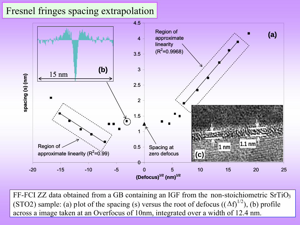
FF-FCI
ZZ data obtained from a GB containing an IGF
from the non-stoichiometric SrTiO3
(STO2) sample: (a) plot of the spacing (s) versus the root of defocus ((f)1/2), (b) profile across a image taken at an Overfocus
of 10nm, integrated over a width of 12.4 nm.

Fresnel
fringes hidden in high-resolution micrographs
Lu-Mg doped Si3
N4
sample
1.3 nm
0.66 nm
1.3 nm
0.66 nm
(a) HRM
10 nm10 nm10 nm10 nm10 nm10 nm
(b) FF-HRM
0 4 8Distance (nm)
FWHM
V V
(Two ways of measuring V V)
Inte
nsity
0 4 8Distance (nm)
FWHM
V V
(Two ways of measuring V V)
Inte
nsity
(c) profile across the GB
2 4Distance (nm) 60
Z Z
V V
Inte
nsity
2 4Distance (nm) 60
Z Z
V V
Inte
nsity
(d) profile across the GB in the FF-HRM

Stoichiometric
SrTiO3
sample
0.75 nm
(a) HRM
10 nm10 nm
(b) FF-HRM
2 3Distance (nm)
10
P P
Inte
nsity FWHM
2 3Distance (nm)
10
P P
Inte
nsity FWHM
(c) profile across the GB in the HRM
2 Distance (nm) 4
Z Z
P P
Inte
nsity
0 2 Distance (nm) 4
Z Z
P P
Inte
nsity
0
(d) profile across the GB in the FF-HRM

Thickness from high-resolution
micrograph (HRt)
Ft-
FWHM
Thickness after Fourier filtering the HRM
(FF-HRt)
(MacLaren thickness)
FF-Ft-
Zero to zero (ZZ)
From High-Resolution Micrograph (HRM)
Fourier Filtered
Raw Image
From profile across grain boundary
Ft-
Peak to peak (PP)/
Valley to valley (VV)
FF-Ft-
Peak to peak (PP)/
Valley to valley (VV)
Schematic showing the measurement of thickness from HRM. Thickness can be calculated directly from the HRM
(HRt) or by Fourier filtering the lattice fringes from the micrograph (FF-HRt). An easier alternative is to use the plot of profiles across these images. Values which correlate with each other are shown either by same shading
or with the same border.

Zero defocus imaging
2 nm2 nm2 nm
A
A
(b)(a)
1.2 nm
2 nm2 nm2 nm
A
A
(b)(a)
2 nm2 nm2 nm
A
A
(b)(a)
1.2 nm
Fourier Filtered-FCI from Si3
N4
–
grain boundary having an IGF
2.76 Å2.76 Å
Zero thickness
-5 0 5Distance (nm)
Zero thickness
-5 0 5Distance (nm)
Dry GB in SrTiO3
(a) HRM, (b) profile across the FF-FCI
showing zero thickness.

Sample(Lattice fringe orientation)
HRt(nm)
FF-HRt(Maclaren
thickness)
(nm)
From intensity (Fresnel) profiles
Ft
(nm)
FF-Ft (nm)
FWHM PP/VV Z-Z PP/VV
Lu doped Si3
N4(parallel to GB on one
side)
1.18 1.95 1.18 1.98-2.6* 1.18 1.98
StoichiometricSrTiO3
(STO1)(not parallel to GB on
either side)
0.95 1.51 0.95 1.53 0.94 1.51
* Depending on the choice of the VV distance
A comparison of the values of thickness obtained from:
High-Resolution Micrograph (HRt)
Plot of intensity profiles across the IGF
revealing Fresnel
fringes (Ft)
Fourier filtered (FF) high-resolution image (MacLaren
thickness (FF-HRt))
FF Fresnel
thickness (FF-Ft)

In-situ Heating Experiments
"The evolution of amorphous grain boundaries during In-situ heating experiments in Lu doped Si3
N4
"
S. Bhattacharyya, Anandh Subramaniam,
C.T. Koch and M. Rühle
Materials Science and Engineering A, 422, p.92, 2006.

In-situ heating experiments in Lu-Mg doped Si3 N4
400 kVJEOL 4000 FX
Lattice fringe imaging
120 kVZEISS-912
Fresnel
fringe techniques
0
100
200
300
400
500
600
700
800
900
1000
0 50 100 150
Time (minutes)
Tem
pera
ture
(ºC
)
JEOL 4000 FXZeiss-912
950ºC, 30 min
950ºC, 1hr 20 min

1.3 nm
0.66 nm
1.3 nm
0.66 nm
0.66 nm
1.3 nm
0.66 nm
1.3 nm
6.6 Å
31 Å
26 Å
6.6 Å6.6 Å
31 Å
26 Å2.2 nm
3.3 nm6.6 Å
22 Å
24 Å
2.2 nm
3.3 nm6.6 Å
22 Å
24 Å
400 kVJEOL 4000 FX
24oC 650oC
950oC24oC

0.8
1.3
1.8
2.3
2.8
3.3
Heating cycle
Thi
ckne
ss o
f the
IGF
(nm
)
650ºC, t=1 hrRT, t=0
Cooled to RT, t=2 hr 25 min
950ºC, t=2 hr 20 min
Wedge shaped IGF with a range of thicknesses
Crystal-1 Crystal-2Crystal-1 Crystal-2
Increased thickness t > tHT RT
Electron beam direction
Crystal-1
tCrystal-2
t1t
Crystal-1 Crystal-2
Wedge Shapedt2
t1
t > t2 1
Crystal-1
hickdary
Crystal-2
ness
Crystal-1 Crystal-2
Non-uniform thickness along the grain boundary
20 nm20 nm20 nm
A
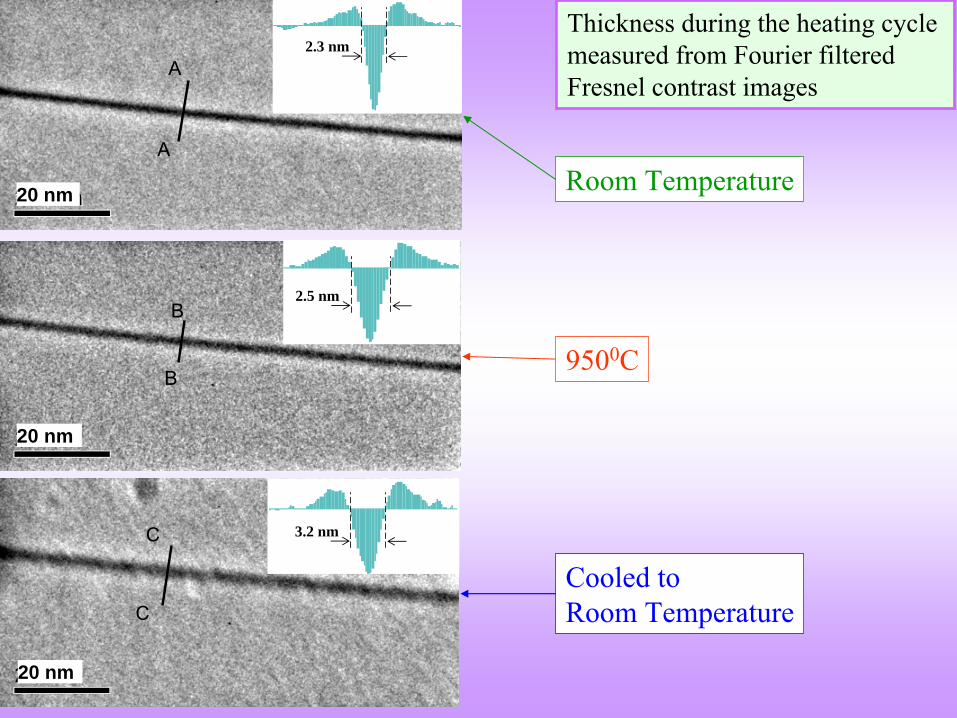
A2.3 nm
20 nm20 nm20 nm
A
A2.3 nm
20 nm20 nm20 nm
B
B
2.5 nm
20 nm20 nm20 nm
B
B
20 nm20 nm20 nm
B
B
2.5 nm
20 nm20 nm20 nm
C
C 3.2 nm
20 nm20 nm20 nm
C
C 3.2 nm
Thickness during the heating cycle measured from Fourier filtered Fresnel
contrast images
Room Temperature
Cooled to Room Temperature
9500C

0
1
2
3
4
5
6
7
8
-2.5 -2 -1.5 -1 -0.5 0 0.5 1 1.5 2(Defocus)1/2 ()1/2
Spac
ing
(nm
)
RTHTCooled to RT
Extrapolation of the Fresnel
through focal series fringe spacing data to obtain the
thickness of the IGF: () RT, () 950ºC & () cooled to RT.
-40 0 40-20 20Distance (Å)
RTHTCooled to RT
-40 0 40-20 20Distance (Å)
RTHTCooled to RT
Comparison of exit wave reconstructed profiles, of the
imaginary part of the inner potential, using zero-defocus Fresnel
fringe images: () RT, (─) 950ºC, (--)
cooled to RT. The FWHM
measured from the profiles gives a measure of
the thickness of the IGF.
Thickness of IGF
using alternate methods

High-resolution (400 kV
microscope)
Fresnel fringes (120 kV microscope)
Temperature
HRt (nm)
ExtrapolationFt
(nm)
From zero-defocus image
(Fourier filtered)
(nm)
By zero-defocus Fresnel
reconstruction (FWHM, nm)
Room Temperature
(24ºC)
1.3
0.8 0.5
2.3 1.8
650ºC 1.3 - - - 950ºC 2.6 - 3.1* 1.0 0.1
2.5** 2.1**
Cooled to 24ºC
2.2 – 2.4 2.1 1.2
3.2 3.0
In-situ heating experiments: Summary of results
* micrograph was taken 1 hr 10 min after reaching 950ºC; ** micrograph was taken 15 min after reaching 950ºC.

In-situ heating experiments:Comparison of high-resolution vs
Fresnel
thicknesses
RT
HT
Cooled to RT
High-resolution
Fresnel

SUMMARY & CONCLUSIONSSUMMARY & CONCLUSIONS
Four new techniques have been developed for the measurement of the thickness
of IGFs:
Fresnel
Fringes hidden in high-resolution micrographs
Zero-defocus imaging
Fourier filtered Fresnel
congrast
imaging
Reconstruction of potential profile based on zero-defocus images
Limitations of the standard Fresnel
fringe extrapolation method are brought out
New finding during in-situ heating: fast changes to IGF thickness (in Lu-Mg doped Si3
N4
) can occur at
comparatively low temperatures (<1000ºC) under low irradiation doses
Low T Superdiffusion?

FINITE ELEMENT ANALYSIS FINITE ELEMENT ANALYSIS AT THE NANOSCALEAT THE NANOSCALE
Growth of Epitaxial Films
Stress Fields and Energetics
of Dislocations

EPITAXIAL THIN FILMSEPITAXIAL THIN FILMS
FILM
SUBSTRATE
INRTERFACIAL EDGE DISLOCATION
~100 Å
~100
EXAMPLES
GeSiSi
GaAsPGaAs
InGaAsGaP
AuAg
CoNi
Semiconductor
Metallic

FINITE ELEMENT ANALYSISFINITE ELEMENT ANALYSIS( Stress free strain)
1.
Constructing a strain-free layer of GeSi
on the Si
substrate
2.
Imposing the coherency at the interface through a lattice misfit strain
3.
Simulation is repeated for successive build-up of the layers to model the growth of the film
Elastic constants for the GeSi
alloy calculated by linear interpolation of values
Anisotropic conditions
Lattice constants at 550 0C –
the growth temperature
FILM
DISLOCATION
Edge dislocation is modelled by feeding the strain (Tdl
) corresponding to the introduction of an extra plane of atoms
b = as
/2 [110]
Tdl
= ((as
[110] + bs
) -
as
[110]) / (as
[110] + bs
) = bs
/3bs
=1/3
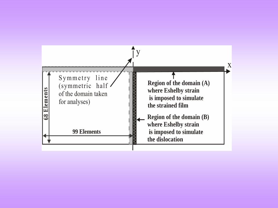
yx
S y m m e t r y l i n e(symmetric half of the domain taken for analyses)
Region of the domain (B)where Eshelby strain is imposed to simulate the dislocation
Region of the domain (A)where Eshelby strain is imposed to simulate the strained film
99 Elements
68 E
lem
ents

GeGe
0.50.5
SiSi
0.50.5
FILM ON FILM ON SiSi
SUBSTRATESUBSTRATE(MISFIT STRAIN = 0.0204)
x
AFTER THE GROWTH OF ONE LAYER ( ~5 Å)
50 Å
230 Å
(MPa)
Zoomed region near the edge
SUBSTRATE
FILM
EDGE
SYMMETRY LINE

GeGe
0.50.5
SiSi
0.50.5
FILM ON FILM ON SiSi
SUBSTRATESUBSTRATE(MISFIT STRAIN = 0.0204)
x
AFTER THE GROWTH OF FIVE LAYERS14
5 Å
190 Å
(MPa)
SYMMETRY LINE
SUBSTRATE
FILM
EDGE

-5.00 -3.00 -1.00 1.00 3.00 5.00
x (Angstroms)
-5.00-4.00-3.00-2.00-1.000.001.002.003.004.005.00
y (A
ngst
rom
s)
-10.00-9.00-8.00-7.00-6.00-5.00-4.00-3.00-2.00-1.000.001.002.003.004.005.006.007.008.009.0010.00
(Contour values x 104 Mpa)
x = 222
22
)()3(
)1(2 yxyxyGb
-5.00 -3.00 -1.00 1.00 3.00 5.00
x (Angstroms)
-5.00-4.00-3.00-2.00-1.000.001.002.003.004.005.00
y (A
ngst
rom
s)
-10.00-9.00-8.00-7.00-6.00-5.00-4.00-3.00-2.00-1.000.001.002.003.004.005.006.007.008.009.0010.00
(Contour values x 104 Mpa)
x = 222
22
)()3(
)1(2 yxyxyGb
x PLOT OF THEORETICAL EQUATION
All contour values are in GPa272Å
272
Å
8.50
3.80
2.86
1.93
1.00
0.05
-9.90
-1.81
-2.75
-3.69
-8.39
x & y original grid size = b/2 = 2.72 Å
All contour values are in GPa272Å
272
Å
8.50
3.80
2.86
1.93
1.00
0.05
-9.90
-1.81
-2.75
-3.69
-8.39
8.50
3.80
2.86
1.93
1.00
0.05
-9.90
-1.81
-2.75
-3.69
-8.39
x & y original grid size = b/2 = 2.72 Å
Sim
ulat
ed
xco
ntou
rs

GeGe
0.50.5
SiSi
0.50.5
FILM ON FILM ON SiSi
SUBSTRATE WITH EDGE DISLOCATIONSUBSTRATE WITH EDGE DISLOCATIONx
AFTER THE GROWTH OF FIVE LAYERS
80 Å
240 Å
MPa
Zoomed region near the edge
FILM
SUBSTRATE
SYMMETRY LINE EDGE

Critical thickness by considering total energy
0.00
1.00
2.00
3.00
4.00
5.00
6.00
7.00
8.00
9.00
0 1 2 3 4 5 6 7 8 9 10 11 12 13 14 15
Number of layers of b/2 thickness (b = 3.84 Å)
Ene
rgy
(x 1
0-9J/
m)
Total energy of the growing film
Total energy of film with dislocaton
Mesh size = (1.92 x 1.92) Å
Domain size = (192 x 134.4) Å
Critical thickness of 20 Å= four film layers
GeGe
0.50.5
SiSi
0.50.5
FILM ON FILM ON SiSi
SUBSTRATESUBSTRATE

Comparison with Comparison with experimental resultsexperimental results
0123456789
0.65 0.7 0.75 0.8 0.85 0.9
x in CuxAu(1-x)
h c (Å
)
Simulation
Theory
Comparison between theory and finite element simulation of the critical thickness for the onset of misfit dislocations in the CuxAu(1-x) /Ni system as a function of copper content x in the film.
8711hc (FEM simulated) (Å)<101013hc (experimental) (Å)
Cr/NiPt/AuCo/CuFilm/Substrate
8711hc (FEM simulated) (Å)<101013hc (experimental) (Å)
Cr/NiPt/AuCo/CuFilm/Substrate
Comparison between FEM simulation and experimental results of critical thickness (hc) for the nucleation of a dislocation in a coherently strained epitaxial film.
Metallic FilmsMetallic Films

5.00
5.50
6.00
6.50
7.00
7.50
8.00
8.50
0 5 10 15 20
Distance from centre (in b spacings)
Tot
al e
nerg
y (x
10-9
J/m
)
Domain Size = (272 x 272) Å
Mesh Size = (2.72 x 2.72) Å
Energy of an edge dislocation as a function of its distance from centre of the domain
All contour values are in GPa
Edge
8.4
3.4
2.4
1.4
0.5
-0.5
-1.4
-2.4
-3.4
-8.4
CENTRE LINE
20b = 109 Å
All contour values are in GPa
Edge
8.4
3.4
2.4
1.4
0.5
-0.5
-1.4
-2.4
-3.4
-8.4
CENTRE LINE
20b = 109 Å
Simulated x contours

Limitations of the current theoriesLimitations of the current theories
The energy of a growing film is assumed to be a linear function of the thickness
The substrate is assumed to be rigid and only the energy of the film is taken into account
Even though the energetics
of the substrate is ignored the energy of the
whole dislocation is taken into account

CONCLUSIONSCONCLUSIONS
Misfit strain is fed as the stress-free Eshelby
strain in the finite
element model to effectively simulate lattice mismatch strain in
an epitaxial layer
Feeding the stress-free strain corresponding to the introduction of an extra plane of atoms can simulate an edge dislocation
The equilibrium critical thickness for epitaxial films can be determined by a combined simulation of a growing film with a edge dislocation (The results obtained show a close correspondence with the standard theoretical expressions and experimental results for epitaxial metallic films)
For the GeSi/Si
system, the experimental values match satisfactorily
with that of the 'threshold approach', when the energy per unit area of the simulated dislocation is taken at a characteristic distance (xch
) of 5b.


Detailed Summary and Conclusions: Microscopy
(i) The utility of Fresnel contrast and high-resolution images can be enhanced by
Fourier filtering the images. This methodology, applied to high-resolution
micrographs, allows the use of images in which lattice fringes are weak (or even
absent) on one side of the IGF and in the case of Fresnel contrast images gives
better interpretability from noisy images.
(ii) A simple new technique is put forth, wherein Fresnel contrast hidden in high-
resolution images are used to objectively demarcate the glass-crystal interface and
to measure the thickness of an IGF (by Fourier filtering the lattice fringe spots).
The optimum mask size was determined by simulations on one-dimensional
scattering potential profiles.
(iii) Experimental results (on Si3N4 doped with Lu-Mg and stoichiometric & non-
stoichiometric SrTiO3) and simulations show that, the plot of fringe spacing (s)
versus root of defocus ((f)1/2) is not linear over the entire defocus range and is
found true at intermediate defocus values. Other limitations of the Fresnel
extrapolation technique are also enumerated; which includes the important
observation that the correct thickness of the IGF is not obtained by the method.

(i) A new methodology is developed, wherein spacing is measured based on Fourier
filtered Fresnel images. Appropriate choice of spacing values from over and
underfocus images, is seen to give a better symmetry in the plots Fresnel fringe
spacing data. It is also seen that this technique gives a better estimate of the
thickness of the IGF from the same set of Fresnel contrast images by extrapolation
to zero-defocus. The approximate validity of the extrapolation method could not be
understood in the framework of the simulations performed.
(ii) Simulations of Fresnel contrast, using one-dimensional potential profiles, are used
for understanding the different sources of left-right (LR) and underfocus-overfocus
(OU) symmetry breaking; which is observed in the experimental Fresnel contrast
images (FCI).
(iv)
(v)

(i) In the light of the limitations of the Fresnel extrapolation method; a new technique
for the Measurement of the thickness of IGFs is illustrated; which is based on
Fourier filtered zero-defocus Fresnel contrast images (tested on Si3N4 doped with
Lu-Mg and non-stoichiometric SrTiO3 samples). This is seen as the simplest
technique for this purpose; wherein, the high-resolution thickness can be estimated,
without actually performing lattice fringe imaging. Simulations are used to validate
the method.
(ii) Thickness measured from lattice fringe imaging (HRt) is equal to the zero-to-zero
distance in the zero-defocus FF-FCI (hidden in HRM or otherwise), which in turn
is a measure of the FWHM of the potential profile (as seen in simulations). This
implies: (a) the HRt corresponds to the FWHM of the potential profile and not the
inner width ('a') or (b) the IGF is fully diffuse. The current work is not able to
differentiate between the two cases.
(vii)
(vi)

(i) Fast changes to IGF thickness (in Lu-Mg doped Si3N4) can occur at comparatively low
temperatures (<1000ºC) under low irradiation doses, with electron beam energies as
low as 120 keV.
(ii) The tendency of the IGFs to regain the width they had before annealing has been
observed. However, the relaxation times were not long enough to observe complete
reversibility of the changes in IGF width.
iii) A tensile-compressive straining cycle may be realized by heating and cooling the
sample due to thermal gradients in the TEM sample, as a result of its special geometry.
(iv) Although local stress vectors, induced by thermal gradients in the sample, may offset
the forces determining the IGF equilibrium width in the force balance model, dynamic
observations (e.g. video recording) of the kinetics of the relaxation process may give
insight into details of diffusion processes and the viscosity of the intergranular glassy
phase.
Detailed Conclusions: In-situ heating
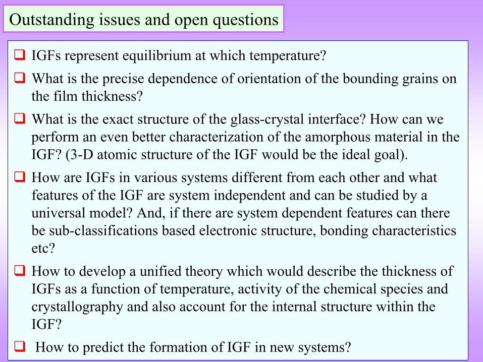
Outstanding issues and open questions
IGFs
represent equilibrium at which temperature?
What is the precise dependence of orientation of the bounding grains on the film thickness?
What is the exact structure of the glass-crystal interface? How can we perform an even better characterization of the amorphous material in the IGF? (3-D atomic structure of the IGF
would be the ideal goal).
How are IGFs
in various systems different from each other and what
features of the IGF
are system independent and can be studied by a universal model? And, if there are system dependent features can
there
be sub-classifications based electronic structure, bonding characteristics etc?
How to develop a unified theory which would describe the thickness of IGFs
as a function of temperature, activity of the chemical species and
crystallography and also account for the internal structure within the IGF?
How to predict the formation of IGF
in new systems?

I. MacLaren, Imaging and thickness measurement of amorphous intergranular films using TEM, Ultramicr. 99 (2004) 103-113.
ReferencesReferences
1. "Intergranular glassy films: an overview" Anandh Subramaniam, Christoph T. Koch, Rowland M. Cannon, and Manfred Rühle Materials Science and Engineering A, 422, p.3, 2006.
2. "Aspects regarding measurement of thickness of Intergranular Glassy Films" S. Bhattacharyya, Anandh Subramaniam, C.T. Koch and M. Rühle Journal of Microscopy, 221, p.46, 2006.
3. "The evolution of amorphous grain boundaries during In-situ heating experiments in Lu doped Si3N4" S. Bhattacharyya, Anandh Subramaniam, C.T. Koch and M. Rühle Materials Science and Engineering A, 422, p.92, 2006.
4. "Assessing thermodynamic properties of amorphous nanostructures by energy filtered electron diffraction" C.T. Koch, S. Bhattacharyya, Anandh Subramaniam, and M. Rühle, Microscopy and Microanalysis, 10, Suppl. 2, p.254, 2004.

Simulation of Fresnel
Contrast

Am
orph
icity
0
1
Direction of the electon beam Crystal Crystal
GlassRough interface
Projected potentialprofile
Inclined IGF
Projected potentialprofile
Glass
Limitations of a one-dimensional projected potential profile, with respect to its ability to distinguish between various structural features in the GB region having an IGF
Diffuse interface between glass and crystal
Rough interface
Inclined interface

Fresnel
fringe profile is obtained as follows: (i) the potential profile V(r) is constructed and multiplied by
and t (ii) the exponential term generated from this is Fourier transformed and multiplied
by the aperture function and MTF in reciprocal space(iii) the product is inverse Fourier transformed to real space
(the square of the absolute value is the Fresnel
intensity profile)
(r)21 iσV t iχ(k)
(r) apI = FT [FT(e )f (k)e ]
I(r)
→ image intensity V(r)
→ potential profile across the interface
→ interaction constant
t → specimen thickness fap
(k) → objective aperture function in reciprocal space ei(k)
→ microscope contrast transfer function (MTF) k → reciprocal lattice vector.
2 3 4s
1χ(k) = πΔfλk + πC λ k2

yxieyxAyxf , ),(),(
f(x,y) → specimen function
→ phase (function of V(x,y,z))
V(x,y,z) → specimen potential Vt
(x,y) → projected potential
→ Interaction constant (=/E)
Phase Object approximation
yxieyxf ,),(
Weak Phase Object approx.
),( 1),( yxVyxf t
dzzyxVyxVt ),,(),(
),( ),( yxVyxVE
d tt
d
V(x,y,z) Specimen
Phase change = f(Vt
)
yxVi teyxf , ),(
WPOA For a very thin specimen the amplitude of the transmitted wave function will be linearly related to the projected potential

Parameter Designation Value / Description
Weak Phase Object
Approximation
WPOA . t = 0.01 V1
( interaction constant, t – specimen thickness)
Phase Object
Approximation
POA . t = 0.1 V1
Potential Profile P FWHM = 20.4 Å, Diffuse interface on both sides
P1 a = a0 = aFWHM = 20.4 Å, square potential well
P2 aFWHM = 20.4 Å, left-right (LR) asymmetric profile
P3 aFWHM (of well) = 20.4 Å, aFWHM (of bump) = 4.5 Å
to simulate segregation
Wavelength () L1 0.0335 Å
Spherical aberration
(Cs)
C1 2.7 mm
Accelerating voltage - 120 kV
Objective aperture Size A0 Diffuse aperture with dFWHM =0.2496 Å1
Mask Size M1 0.026 Å1 (diameter)
M2 0.032 Å1 (diameter)
M3 Mask with diffuse edges dFWHM = 0.026 Å1
Beam sampling size - 0.23 Å
Simulation cell size - 126.73 Å
Parameters and assumptions used in the simulations of FCI and FF-FCI.

Potential Profile (scale for x-axis is in Å)
(comments)
Fresnel contrast plots (comments)
20.4 Å
0 V
6.44 V
20.4 Å
0 V
6.44 V
Standard square potential well) P1
(WPOA)
overfocus 2.2 micrometerunderfocus 2.2 micrometer
20 60Distance (Å)
-20 0-60 -40 40-80 80
Underfocus
Overfocus
A
A
overfocus 2.2 micrometerunderfocus 2.2 micrometer
20 60Distance (Å)
-20 0-60 -40 40-80 8020 60Distance (Å)
-20 0-60 -40 40-80 80
Underfocus
Overfocus
A
A
(LR symmetry present and OU symmetry is approximate)
20.4 Å
0 V
6.44 V
20.4 Å
0 V
6.44 V
P1 (POA)
overfocus 2.2 micrometerunderfocus 2.2 micrometer
20 60Distance (Å)
-20 0-60 -40 40-80 80
Underfocus
Overfocus
A
A
Shift in positionOf the peak
overfocus 2.2 micrometerunderfocus 2.2 micrometer
20 60Distance (Å)
-20 0-60 -40 40-80 8020 60Distance (Å)
-20 0-60 -40 40-80 80
Underfocus
Overfocus
A
A
A
A
Shift in positionOf the peak
(OU symmetry broken)
Effect of various IGF potential profiles and assumptions on the Fresnel
contrast image (FCI)
WPOA-Weak Phase Object Approximation
Defocus of
2.2 mCs = 2.7 mm
0 V
FWHM= 20.4 Å
6.44 V
-20 0 20-40 40
0 V
FWHM= 20.4 Å
6.44 V
-20 0 20-40 40 (Profile with Left-Right
asymmetry) P2
(WPOA) 4
6
8
2
4
6overfocus 2.2 micrometerunderfocus 2.2 micrometer
20 60Distance (Å)
-20 0-60 -40 40-80 80
Underfocus
Overfocus
AA
BB
4
6
8
2
4
6overfocus 2.2 micrometerunderfocus 2.2 micrometer
20 60Distance (Å)
-20 0-60 -40 40-80 8020 60Distance (Å)
-20 0-60 -40 40-80 80
Underfocus
OverfocusOverfocus
AA
AA
BB
(LR symmetry broken)
4.5 Å
0 V
6.44 V
FWHM= 20.4 Å
-20 0 20 40
4.5 Å
0 V
6.44 V
FWHM= 20.4 Å
-20 0 20 40
(Profile reflecting segregation) P3
(WPOA) 20 60Distance (Å)
-20 0-60 -40 40-80 80
Underfocus
Overfocus
A A
B B
20 60Distance (Å)
-20 0-60 -40 40-80 8020 60Distance (Å)
-20 0-60 -40 40-80 80
Underfocus
OverfocusOverfocus
A A
B B
(LR symmetry broken)
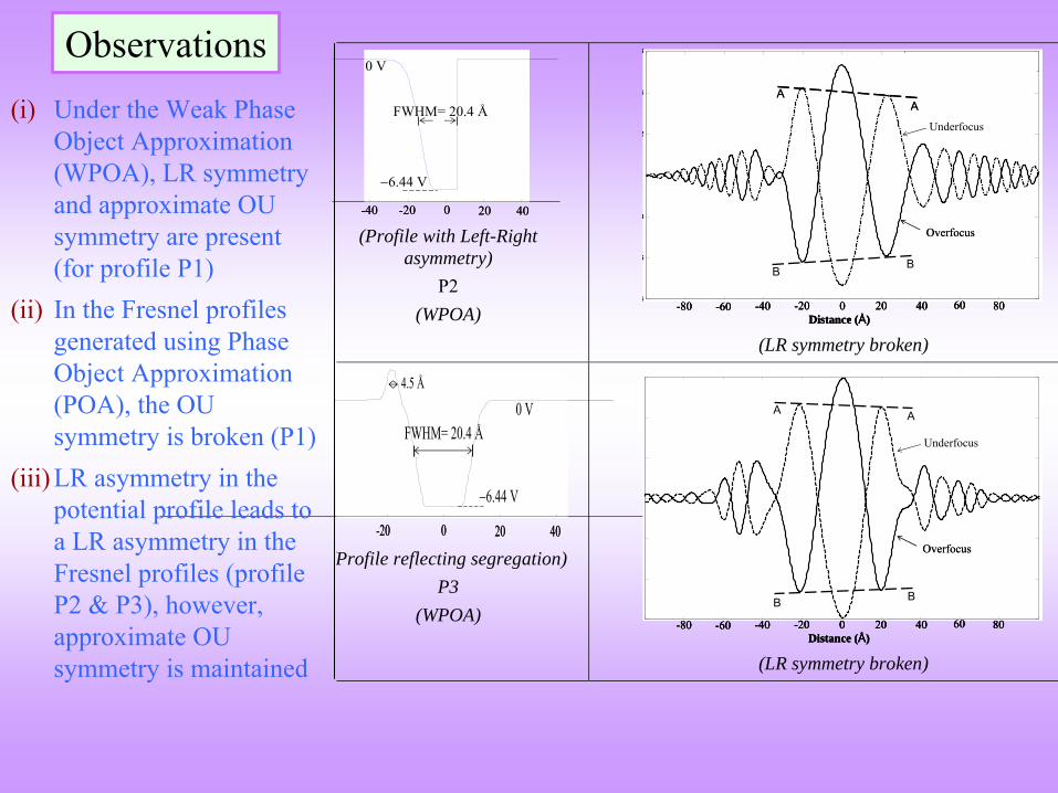
(i)
Under the Weak Phase Object Approximation (WPOA), LR
symmetry and approximate OU
symmetry are present (for profile P1)
(ii)
In the Fresnel
profiles generated using Phase Object Approximation (POA), the OU
symmetry is broken (P1)
(iii)
LR
asymmetry in the potential profile leads to a LR
asymmetry in the Fresnel
profiles (profile P2 & P3), however, approximate OU
symmetry is maintained
Observations

High Resolution Microscopy

)( ),( rfyxf
)( ),( rgyxg
)(rh
Point spread function )(uHContrast transfer function
Specimen
Image
Diffraction patternBack focal plane
( )F u
( )G u
Rea
l spa
ceR
eciprocal space
• The Point Spread Function (PSF) is also called the Impulse Response Function (IRF)• The Contrast Transfer Function (CTF) is also called the Modulation Transfer Function (MTF)
Fourier transform

Every imaging device is characterized by its Transfer Function (CTF) (Band filter)
This describes the magnitude with which a spatial frequency g
is
transferred through the device
Image formation in an TEM is a coherent process Object and Transfer functions are complex functions with amplitude and phase
1/
→
1
<N> Noise
→ resolution
PSF→ )(rh
CTF
→ )(uH
IDEAL

2 ) ()(
432 uCufu s
)()()( rhrfrg
)()()( uFuHuG
Point spread function
Convolution in real space gives multiplication in reciprocal space
Contrast transfer function
Aperture function
Envelope function
Aberration function
)()()()( uBuEuAuH
Property of lens
) , , ,()( sCuffu
)](exp[)( uiuB
Specimen transmission function
Phase distortion function

Point spread function
Specimen transmission function
Image
Effect of point spread function on image
Reference: Electron Microscopy- Principles and Fundamentals, Eds.: S. Amelinckx, D. van Dyck, J. van Landuyt, G. van Tendeloo, VCH, Weinheim, 1997
A measure of the resolution

High resolution implies ability to see two closely spaced features in the sample (real ‘r’
space) as distinct
This corresponds to high spatial frequencies large distances from the optic axis in the diffraction pattern (reciprocal (u) space)
Rays which pass through the lens at such large distances are bent through a larger angle by the objective lens
Due to an imperfect lens (spherical aberration) these rays are not focused at the same point by the lens
Point in the sample disc in the image (spreading of a point in the image)
Objective lens magnifies the image but confuses the detail (hence the resolution is limited)
Each point in the final image has contributions from many points
in the specimen (no linear map between the specimen and the image)
Is a linear relationship possible?

( ) ( ) i rf r A r e
f(r) → specimen function
→ phase (function of V(x,y,z))
V(x,y,z) → specimen potential Vt
(x,y) = Vt
(r) → projected potential
→ Interaction constant (=/E)
Phase Object approximation
( ) i rf r e
Weak Phase Object approx.
( ) 1 ( )tf r i V r
d
V(x,y,z) Specimen
Phase change = f(Vt
)
( ) ti V rf r e
Specimen and approximations
[ ( )]( ) ti V r rf r e
dzzyxVyxVt ),,(),(
( ) ( )t td V r V rE
Including absorption
2 3 4
11! 2! 3! 4!
x x x x xe

( ) 1 ( )tf r i V r
WPOA For a very thin specimen the amplitude of the transmitted wave function will be linearly related to the projected potential
Phase object has become
and amplitude object
The TEM operated in the phase contrast mode at optimum focus directly reveals the projected potential (under WPOA
= very thin specimen)
( ) 1 ( )r i r
Central beamDiffracted beam
If the phase of the diffracted beam is shifted by /2 w.r.t the central beam the amplitudes of the diffracted beam are multiplied by exp(i/2) = i
( ) 1 ( )r r
1 2 ( )I r The phase of the object is directly imaged

meEh
2In vacuum
),,((2'
zyxVEmeh
In the specimen
dzdzd
22'
Phase change dzzyxVE
d ),,( dzzyxVd ),,(
( , ) ( , , ) ( )t tV x y V x y z dz V r ( ) ( )t td V r V rE
→ Interaction constant (=/E) tends to a constant value as V increases(energy of electron proportional to E & 1, variables tend to compensate)

POA
holds good only for thin specimens
If specimen is very thin {Vt
(r) << 1} WPOA
In WPOA
{f(r) = 1
i
Vt
(r)} the amplitude of the transmitted wave will be linearly related to the projected potential of the specimen
(the TEM in the phase contrast mode at optimum focus directly reveals the projected potential)
Hence if object is very thin, optimum focus imaging would directly reveal atoms as dark areas and empty spaces as light
For Ti2 Nb10 O27 WPOA is valid if specimen thickness < 6Å [Fejes.P.L., Acta Cryst. A33, 109, 1977]
For thick specimens, there may not be a one to one correspondence between the projected structure of the object and exit face wavefunction

)()()( rhrfrg
( ) [1 ( )] ( )tr i V r h r
WPOA
( ) [1 ( )] [ ( ) ( )]tr i V r Cos r i Sin r
1 2 ( )] ( )tI V r Sin r
I =
.* Neglecting 2
Only imaginary part of B(u) contributes
to intensity
)](exp[)( uiuB )]([2)( uSinuB
22 ( )( ) 1i rI r e
In an ideal microscope the image wavefunction
= object wavefunctionImage intensity for a pure phase object
The image would show no contrast
This is like imaging a variable thickness glass plate in an ideal light microscope
( ) 1 ( ) ( ) ( ) ( )t tr V r Sin r i V r Cos r
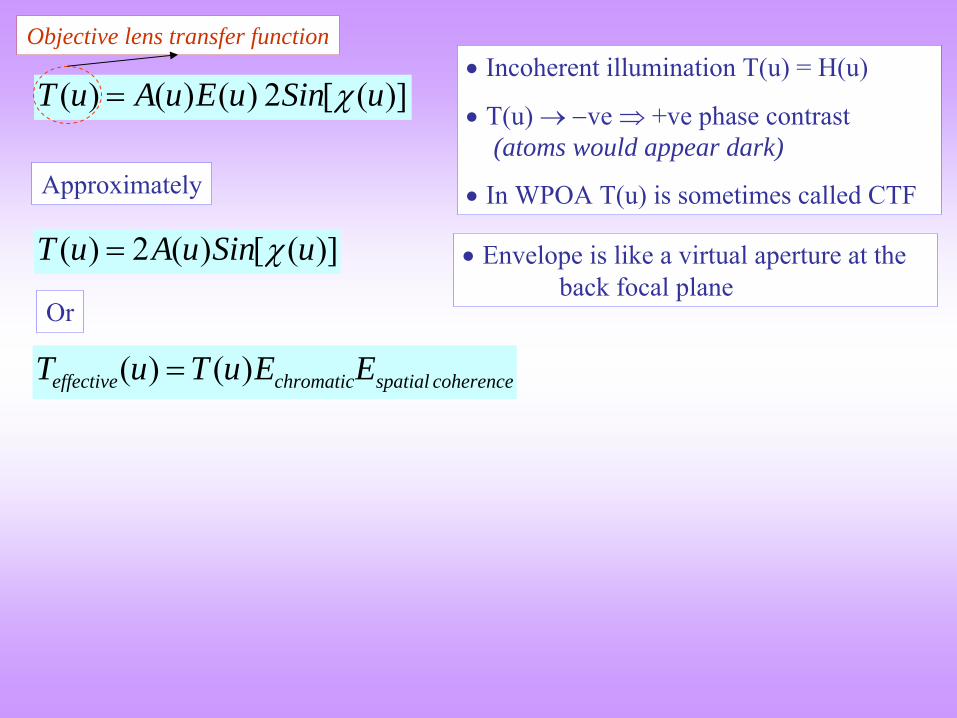
)]([2 )()()( uSinuEuAuT
Objective lens transfer function Incoherent illumination T(u) = H(u)
T(u) ve
+ve
phase contrast (atoms would appear dark)
In WPOA
T(u) is sometimes called CTFApproximately
)]([)(2)( uSinuAuT
Or
coherencespatialchromaticeffective EEuTuT )()(
Envelope is like a virtual aperture at the back focal plane
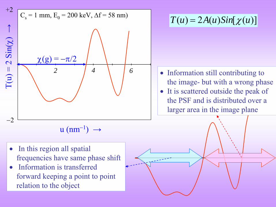
u (nm1)
→
T(u)
= 2
Sin
()→
+2
2
v
2 4 6
Cs
= 1 mm, E0
= 200 keV, f = 58 nm)
(g) = /2
In this region all spatial frequencies have same phase shift
Information is transferred forward keeping a point to point relation to the object
Information still contributing to the image-
but with a wrong phase
It is scattered outside the peak of the PSF
and is distributed over a larger area in the image plane
)]([)(2)( uSinuAuT

u (nm1)
→
T(u)
= 2
Sin
()→
Cs
= 2.2 mm, E0
= 200 keV, f = -100 nm)
)]([)(2)( uSinuAuT
T eff
ectiv
e(u)→
u (nm1)
→
coherencespatialchromaticeffective EEuTuT )()(
Scherzer
defocus and Information Limits 124
3Scherzer sf C
1 34 4
Scherzer su =1.51 C
1 34 4
Scherzer s= 0.66 C r
Instrumental resolution limit can use nearly intuitive arguments to interpret the contrast
Information limit
Damping envelope

Instrumental resolution limit (Point resolution / Structural resolution) finest detail that can be interpreted in terms of the structure
can use nearly intuitive arguments to interpret the contrast
The point resolution can be improved by
↓
Cs
↓
(= ↑
accelerating voltage)
Information limit finest detail that can be resolved by the instrument
(irrespective of an possible interpretation) corresponds to the maximal diffracted beam angle that is still transmitted
with appreciable intensity the TEM (transfer function) is a low pass filter (in g) which cuts off all
information beyond the information limit
The information limit can be improved by
Improving beam coherence
↓
(= ↑
accelerating voltage)
Convolution
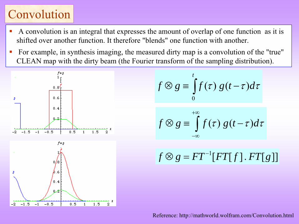
A convolution is an integral that expresses the amount of overlap of one function as it is shifted over another function. It therefore "blends" one function with another.
For example, in synthesis imaging, the measured dirty map is a convolution of the "true" CLEAN map with the dirty beam (the Fourier transform of the sampling distribution).
Reference: http://mathworld.wolfram.com/Convolution.html
0
( ) ( )t
f g f g t d
( ) ( )f g f g t d
1[ [ ] . [ ]]f g FT FT f FT g

Zero-Defocus Fresnel
Reconstruction

The intensity of an image is given as:
2( ) MTF(r)I r r
(r) → Complex electron exit-face wave function I (r) → Intensity of the imageMTF(r) → Microscopic transfer function. V(r) → Complex projected potential
→ Interaction constant (=/E) t
→ Specimen thickness
Using phase object approximation
Ψ( ) exp i tV(r) exp (́ ) ´́ ( )r i t V r iV r
The real part of the scattering potential (V'(r)) is due to elastic interaction of the electron with the specimen and the imaginary part (V''(r)) describes the loss of electrons from the elastic channel (and thus the zero energy filtered image), due to inelastic scattering events.

For zero-defocus imaging (and the assumed ideal aberration free imaging conditions; which is expected to hold good for the low-resolution conditions in a microscope like Zeiss-912) the following can be set:
aperture
aperture
qqqq
qmtfrMTFFT
,0,1
)(
qaperture
→ Reciprocal-space radius of the top had aperture
function
Ignoring coherent aberrations and envelope functions related to chromatic aberration, partial spatial coherence and microscope instabilities; the following equation is obtained under zero-defocus conditions:
2
2I exp ´´ 1 exp ´ exp ´´ ´́ ´
apertureq
r t V r i tV r t V r V r
´́ ´ , ln 1 exp ´aperture
apertureq
V r q i t V r
V'''(r,qaperture
)
→ a specimen and objective aperture dependent ‘pseudo-absorptive’
scattering potential

Both the inelastic scattering described by V''(r) and the pseudo-absorptive by V'''(r) increase with the atomic number (Z) of the scattering element.
In fact, the high-angle annular dark-field scanning transmission electron microscopy (HAADF
STEM) technique, being mainly based on V'''(r), is also called Z-
contrast STEM for this reason.
Vabs
(r) = V''(r) + V'''(r)
The Fresnel
contrast due to variations in the electrostatic potential V'(r, q<qaperture
) across the IGF
vanishes at zero-defocus so that:
1´´ ´´´ ln ln2
t V r V r I r I r
t and
are taken to be constant The LHS is representative of the inelastic and high-angle scattering and thus
the concentration of heavy elements at position. The FWHM
of a profile of absorptive potential across the IGF
gives a measure of its chemical thickness.
The resolution of this method is limited by the size of objective aperture (in Zeiss-912 microscope this is equal to 8 Å).

MATLAB
R12 software was used for implementing the algorithm to determine the imaginary part of the potential profile across the interface
from zero-defocus images.

-40 0 40-20 20Distance (Å)
RTHTCooled to RT
20 nm20 nm20 nm
A
A2.3 nm
20 nm20 nm20 nm
B
B
2.5 nm
20 nm20 nm20 nm
C
C 3.2 nm
RT
HT
Cooled to RT
FRESNELFRESNEL
RECONSTRUCTIONRECONSTRUCTION
Exit face wave reconstructed profiles, of the imaginary part of the inner potential, using
zero-defocus Fresnel
fringe images

1.5
1.6
1.7
1.8
1.9
2
2.1
2.2
2.3
2.4
-30 -20 -10 0 10 20 30(Defocus)1/2 (nm)1/2
spac
ing
(s) (
nm)
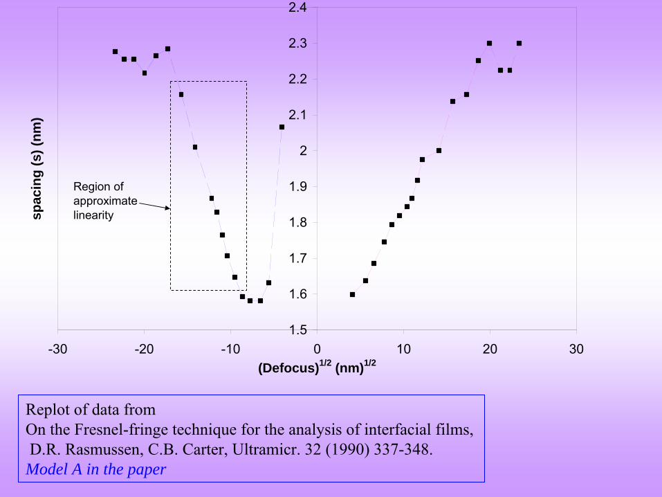
Region of approximatelinearity
Replot
of data fromOn the Fresnel-fringe technique for the analysis of interfacial films, D.R. Rasmussen, C.B. Carter, Ultramicr. 32 (1990) 337-348.Model A in the paper

1/length scale
Dep
ende
nce
on a
ssum
ptio
ns
Force balance Adsorption/Wetting
Diffuse Interface
Phase Field Method
Classical Density Functional Methods
First Principles Methods
Molecular Dynamics/Monte Carlo
1/length scale
Dep
ende
nce
on a
ssum
ptio
ns
Force balance Adsorption/Wetting
Diffuse Interface
Phase Field Method
Classical Density Functional Methods
First Principles Methods
Molecular Dynamics/Monte Carlo

Atomic-resolution scanning transmission electron microscope (STEM) images ofan intergranular
glassy film (IGF) in La-doped -Si3
N4
:a) High-angle annular dark-field (HAADF-STEM)b) Bright-field (BF-STEM)
N. Shibata, S.J. Pennycook, T.R. Gosnell, G.S. Painter, W.A. Shelton, P.F. Becher
“Observation of rare-earth segregation in silicon nitride ceramics at subnanometre
dimensions”
Nature 428 (2004) 730-33.
(a) (b)[0001]

HAADF-STEM images of the interface between the IGF
and the prismatic surface of an -
Si3
N4
grain. The -Si3
N4
lattice structure is superimposed onthe images. a) La atoms are observed as the bright spots (denoted by red arrows) at theedge of the IGF. The positions of La atoms are shifted from that of Si
atoms based on theextension of the -Si3
N4
lattice structure; these expected positions are shown by opengreen circles. b) reconstructed image of a, showing the La segregation sites more
clearly. The predicted La segregation sites obtained by the first-principles calculations are shown by the open white circles.
N. Shibata, S.J. Pennycook, T.R. Gosnell, G.S. Painter, W.A. Shelton, P.F. Becher
“Observation of rare-earth segregation in silicon nitride ceramics at subnanometre
dimensions”
Nature 428 (2004) 730-33.

HAADF-STEM images of La-, Sm-, Er-, Yb-, and Lu-doped Si3
N4
:The attachment of heavy atoms in the form of atomic columns oriented normal to the image plane
A. Ziegler, J.C. Idrobo, M.K. Cinibulk, C. Kisielowski, N.D. Browning, R.O. Ritchie, “Interface Structure and Atomic Bonding Characteristics in Silicon Nitride Ceramics”
Science 306 (2004) 1768-70

Coincident Site Lattice
Centre of Rotation
Rotation by 36 52'

The Coincident Site Lattice
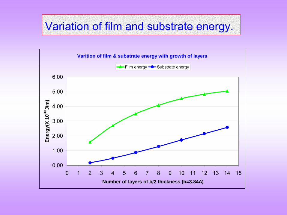
Variation of film and substrate energy.
Varition of film & substrate energy with growth of layers
0.00
1.00
2.00
3.00
4.00
5.00
6.00
0 1 2 3 4 5 6 7 8 9 10 11 12 13 14 15Number of layers of b/2 thickness (b=3.84Å)
Ener
gy(X
10-1
0 J/m
)
Film energy Substrate energy

Limitations of the current theoriesLimitations of the current theories
The energy of a growing film is assumed to be a linear function of the thickness
The substrate is assumed to be rigid and only the energy of the film is taken into account
Even though the energetics of the substrate is ignored the energy of the whole dislocation is taken into account

Advantages of the current simulationAdvantages of the current simulation
(i) As growth progresses, the upper layers are expected to be more relaxed energetically as compared to the layers closer to the substrate and this aspect is captured in the simulation
(ii) The simulation calculates the energy of the interfacial dislocation in a film/substrate system (with separate material properties for the film and substrate), wherein there is considerable asymmetry between the tensile and compressive stress fields of the dislocation and hence the energy of a interfacial dislocation is different from that of a dislocation in a bulk crystal
(iii) The methodology adopted automatically takes into account the interaction between the film coherency and dislocation strain fields,
(iv) Equilibrium critical thickness is calculated taking into account the energy of the entire system and not just the film as in many models.

Limitations of the current simulationLimitations of the current simulation
(i)
E and
values calculated from single crystal data (bulk values) have been used for the thin films
(ii)
Linear interpolation is used to calculate the lattice parameter and the material properties of the alloy films
(iii)
For computational convenience the thickness and width of the substrate considered is small as compared to the real physical dimensions
(iv)
For computational convenience and for comparison with available experimental data highly strained films have been considered in the current analysis and the model will have to be tested for low strain systems wherein the critical thickness values are very large
(v)
Core structure & energy of the dislocation are ignored in the simulation.

Copyright © 2022 FDOKUMEN


![Microscopic and macroscopic creativity [Comment]](https://static.fdokumen.com/doc/165x107/63222cba63847156ac067f99/microscopic-and-macroscopic-creativity-comment.jpg)