Carbon Nanotube Spin-Valve with Optimized Ferromagnetic ...
124
Carbon Nanotube Spin-Valve with Optimized Ferromagnetic Contacts Inauguraldissertation zur Erlangung der W¨ urde eines Doktors der Philosophie vorgelegt der Philosophisch-Naturwissenschaftlichen Fakult¨ at der Universit¨ at Basel von Hagen Matthias Aurich aus Deutschland Basel, 2012
-
Upload
khangminh22 -
Category
Documents
-
view
3 -
download
0
Transcript of Carbon Nanotube Spin-Valve with Optimized Ferromagnetic ...

Carbon Nanotube Spin-Valve with
Optimized Ferromagnetic Contacts
Inauguraldissertation
zurErlangung der Wurde eines Doktors der Philosophie
vorgelegt derPhilosophisch-Naturwissenschaftlichen Fakultat
der Universitat Basel
von
Hagen Matthias Aurichaus Deutschland
Basel, 2012

Genehmigt von der Philosophisch-Naturwissenschaftlichen Fakultatauf Antrag vonProf. Dr. C. SchonenbergerProf. Dr. B. HickeyDr. A. Baumgartner
Basel, 18. Oktober 2011
Prof. Dr. Martin SpiessDekan

Contents
Introduction vii
1 Theoretical Background 11.1 Ferromagnetism . . . . . . . . . . . . . . . . . . . . . . . . . . 1
1.1.1 Exchange interaction . . . . . . . . . . . . . . . . . . . 11.1.2 Stoner model of ferromagnetism . . . . . . . . . . . . 31.1.3 Magnetic anisotropy and domains . . . . . . . . . . . 61.1.4 Stoner-Wohlfarth model . . . . . . . . . . . . . . . . . 8
1.2 Magnetoresistance effects in standard structures . . . . . . . 91.2.1 Spin injection, accumulation and detection . . . . . . 91.2.2 Anisotropic magnetoresistance . . . . . . . . . . . . . 121.2.3 Spin-valve structures . . . . . . . . . . . . . . . . . . . 121.2.4 Tunnel magnetoresistance . . . . . . . . . . . . . . . . 131.2.5 Spin field-effect transistor . . . . . . . . . . . . . . . . 15
1.3 Carbon nanotube quantum dots . . . . . . . . . . . . . . . . . 161.3.1 Electronic properties of a graphene sheet . . . . . . . 161.3.2 Rolling up graphene into a nanotube . . . . . . . . . . 181.3.3 Quantized transport in CNT quantum dots . . . . . . 20
2 Sample Fabrication and Measurements at Cryogenic Temperatures 252.1 Wafer preparation . . . . . . . . . . . . . . . . . . . . . . . . 252.2 Carbon nanotube growth . . . . . . . . . . . . . . . . . . . . 262.3 Device fabrication . . . . . . . . . . . . . . . . . . . . . . . . 272.4 Improving the electrical contact to CNTs . . . . . . . . . . . 312.5 Measurement set-up . . . . . . . . . . . . . . . . . . . . . . . 352.6 Cryogenics . . . . . . . . . . . . . . . . . . . . . . . . . . . . . 37
iii

iv Contents
3 Ferromagnetic Materials for Carbon Nanotube Spintronic Devices 393.1 Methods of investigation . . . . . . . . . . . . . . . . . . . . . 40
3.1.1 Vibrating sample magnetometer . . . . . . . . . . . . 403.1.2 Anisotropic magnetoresistance . . . . . . . . . . . . . 41
3.2 Ferromagnetic Materials . . . . . . . . . . . . . . . . . . . . . 433.2.1 Ni . . . . . . . . . . . . . . . . . . . . . . . . . . . . . 433.2.2 Co . . . . . . . . . . . . . . . . . . . . . . . . . . . . . 443.2.3 Fe . . . . . . . . . . . . . . . . . . . . . . . . . . . . . 453.2.4 PdNi . . . . . . . . . . . . . . . . . . . . . . . . . . . . 483.2.5 PdNi/Co . . . . . . . . . . . . . . . . . . . . . . . . . 493.2.6 PdFe . . . . . . . . . . . . . . . . . . . . . . . . . . . . 503.2.7 NiFe (Permalloy) . . . . . . . . . . . . . . . . . . . . . 51
3.3 Conclusion . . . . . . . . . . . . . . . . . . . . . . . . . . . . 58
4 Permalloy-based CNT Device 614.1 Formation of quantum dots . . . . . . . . . . . . . . . . . . . 614.2 CNT spin-valve . . . . . . . . . . . . . . . . . . . . . . . . . . 66
4.2.1 Relation of the TMR to contact switching effects . . . 664.2.2 Tunability of the TMR signal . . . . . . . . . . . . . . 674.2.3 Modelling of TMR in a QD spin-valve . . . . . . . . . 69
4.3 Non-local geometry - preliminary results . . . . . . . . . . . . 744.4 Discussion of other magnetoresistance effects . . . . . . . . . 774.5 Conclusion . . . . . . . . . . . . . . . . . . . . . . . . . . . . 80
5 Summary and Outlook 83
A Additional Fabrication Information and Processing Recipies 97A.1 Wafer properties . . . . . . . . . . . . . . . . . . . . . . . . . 97A.2 Wafer cleaning . . . . . . . . . . . . . . . . . . . . . . . . . . 97A.3 Catalyst . . . . . . . . . . . . . . . . . . . . . . . . . . . . . . 98A.4 Chemical vapor deposition . . . . . . . . . . . . . . . . . . . . 98A.5 E-beam resist . . . . . . . . . . . . . . . . . . . . . . . . . . . 98A.6 E-beam lithography . . . . . . . . . . . . . . . . . . . . . . . 99A.7 Ar plasma etching . . . . . . . . . . . . . . . . . . . . . . . . 99
B Improving the Contact Properties of Permalloy - Additional Infor-mation 101B.1 Polymer residues on the CNT contact area . . . . . . . . . . 101B.2 Aluminum oxide interlayer - preliminary results . . . . . . . . 104B.3 Electrical instabilities . . . . . . . . . . . . . . . . . . . . . . 106
List of symbols and abbreviations 107

Contents v
Publication List 111
Curriculum Vitae 113
Acknowledgements 115

vi Contents

Introduction
Technological progress leads to a continuous miniaturization of electroniccomponents, permanently on the search for alternatives to increase the in-formation density of storage devices, to make electronic devices faster andto reduce dissipation in electronic circuits [1]. Unlike conventional electronicdevices, based on charge transport, spin electronic or spintronic devices alsouse the electron spin degree of freedom to control electron transport [2, 3].This offers interesting possibilities of new types of electronic devices1 ase.g. the spin-valve, a hybride structure of ferromagnetic and non-magneticmaterials.
In 1988 Peter Grunberg [5] and Albert Fert [6] discovered independentlythat the electrical resistance of a ferromagnetic metal - normal metal multilayer structure strongly depends on the magnetic configuration of the dif-ferent layers controlled by an external magnetic field. This discovery wasthe basis for huge progress in computer hard disk technology [7] and bothauthors received the Nobel prize in physics in 2007 [8]. Later it was foundthat replacing the metallic interlayer by a non-magnetic insulator can fur-ther increase this magnetoresistance effect due to spin conserving tunnellingof the electrons as proposed by Julliere [9].
However, spin-valves are not only interesting in the computer industrybut also offer new possibilities in basic nanoscience research. A spin polar-ized current can be injected from a ferromagnetic material into a nanoscalestructure allowing the investigation of spin transport and spin dynamics ina solid state environment [10] and offers an additional degree of freedom fortransport spectroscopy [11].
In this thesis we investigate spin-transport in carbon nanotube (CNT)spin-valve devices. CNTs can be imagined as a small sheet of hexagonalarranged carbon atoms, called graphene, rolled up into a seamless cylinder
1Spintronics is a wide research field, also including the fields of spin-based quantumcomputation and communication [4]. In this thesis we focus on magnetoresistancedevices.
vii

viii Introduction
with typical diameters of a few nanometers [12]. They were discovered byS. Iijima in 1991 [13] and are the subject of theoretical and experimentalstudies ever since [14, 15]. CNTs are interesting for spin-transport becausethe spin-dephasing during transport is low due to the absence of nuclear spinin the main carbon isotope 12C and the weak spin-orbit interaction [12]. Inaddition, CNTs allow to fabricate quantum dots coupled to ferromagneticleads. Charging interaction effects on the magnetoresistance can be veryimportant in transport measurements [16] and it can even be possible tocombine spintronics with single electron electronics [17]. Early experimentswith CNT devices already showed that spin-dependent transport is possible[18], before Sahoo et al. reported on the first CNT sample with ‘electricfield control of spin transport’ [19].
Fabricating spin transport devices with CNTs is still problematic and theyield of good devices is low. On the one hand, the ferromagnetic materialused for contacting should provide reliable magnetic properties. On theother hand, the electrical contact properties to CNTs should be good andreproducible. Therefore, a main goal of this thesis is to find a ferromagneticmaterial that fulfils those requirements and to study spin transport in CNTdevices with ferromagnetic contacts.
The thesis is structured as follows:
• Chapter 1The theoretical background for this thesis including ferromagnetism,magnetoresistance devices and carbon nanotube quantum dots is pro-vided.
• Chapter 2We present the sample fabrication methods including carbon nanotubegrowth, lithographic structuring and metal deposition and give a shortoverview of the experimental set-ups.
• Chapter 3Different ferromagnetic materials are investigated for their suitabilityas contact materials for carbon nanotubes.
• Chapter 4A Permalloy-based carbon nanotube device is studied and local andnon-local magnetoresistance signals are presented.
• Chapter 5We summarize the results of this thesis and give an outlook to furtherexperiments.

Chapter 1Theoretical Background
This chapter provides a description of the basic building blocks of a car-bon nanotube spin-valve. For the ferromagnetic contacts an introduction inferromagnetism is provided, before we describe magnetic anisotropies anddiscuss the formation of domains in ferromagnetic materials. In the magne-toresistance section, spin transport effects are introduced and several devicesmaking use of magnetoresistance effects are presented. The last part of thechapter deals with the electronic structure of carbon nanotubes and theformation of quantum dots at low temperatures.
1.1 Ferromagnetism
In a solid, the collective ordering of the electron spins can give rise to perma-nent magnetism. A ferromagnet (FM) shows a specific ordering where all themagnetic moments are aligned in parallel. This phenomenon is caused by theexchange interaction between different magnetic moments. The exchange in-teraction is a consequence of the Coulomb interaction between electrons andthe symmetrization postulate (Pauli principle) as shown below.
1.1.1 Exchange interaction
To give a qualitative explanation of the exchange interaction, we first con-sider the simple two-electron system of the H2 molecule. The coordinates ofthe two electrons and the two nuclei are ri andRi with i = 1, 2, respectively,as illustrated in fig. 1.1. The Hamiltonian of the system can be written asthe sum of two central field Hamiltonians H1
atom and H2atom describing the
1

2 Theoretical Background
r1 r2
R1 R2
+e +e
-e -e
Figure 1.1: Schematic repre-sentation of the assumed two-electron system. The electronsand the nuclei have the coordi-nates ri and Ri with i = 1, 2,respectively.
interaction of electron 1 (2) with nucleus 1 (2) and an interaction Hamilto-nian H′ including the interactions of the electrons with the other nucleus,nucleus-nucleus interaction and electron-electron interaction [20]
H(r1, r2) = H1atom +H2
atom +H′. (1.1)
For two undistinguishable electrons the spatial wavefunctions φ can bewritten in terms of a symmetrized and an antisymmetrized product stateunder particle exchange. Due to the fermion character of the electrons, thePauli principle requires that the total wave function (including the spin part)must be antisymmetric. By first neglecting the electron-electron interactionterm in H′, in the so-called Heitler-London approximation, the total wavefunctions are found1
ψS =1√
2(1 +O)[φ1(r1)φ2(r2) + φ1(r2)φ2(r1)] · χS
ψT =1√
2(1−O)[φ1(r1)φ2(r2)− φ1(r2)φ2(r1)] · χT (1.2)
In the first equation the spatial part of the wavefunction is symmetric andthe spin part of the wavefunction χ is in an antisymmetric singlet state (S).In the second equation the spatial wavefunction is antisymmetric and thespin part is in a symmetric tripet state (T).
1√2(|↑↓〉 − |↓↑〉) singlet state χS
|↑↑〉1√2(|↑↓〉+ |↓↑〉) triplet state χT
|↓↓〉
O = 〈φ1(r1)φ2(r2)|φ1(r2)φ2(r1)〉 describes the double overlap integral ofthe two individual wave functions. The total energies in the singlet and the
1In this independent electron approximation the ionic terms of the wave function areomitted [20].

1.1. Ferromagnetism 3
triplet states are
ES =
⟨ψS |H|ψS
⟩〈ψS |ψS〉 = 2E0 +
C +X
1 +O(1.3)
and
ET =
⟨ψT |H|ψT
⟩〈ψT |ψT 〉 = 2E0 +
C −X1−O (1.4)
with E0 =⟨φ1(r1)|H1
atom|φ1(r1)⟩
=⟨φ2(r2)|H2
atom|φ2(r2)⟩
the atomic en-ergy, C = 〈φ1(r1)φ2(r2)|H′|φ1(r1)φ2(r2)〉 the Coulomb integral and X =〈φ1(r1)φ2(r2)|H′|φ1(r2)φ2(r1)〉 the exchange integral. The energy differencefor the singlet and the triplet state is calculated to
ES − ET = 2X −OC1−O2
≡ 2J (1.5)
J is called the exchange constant. Depending on J either the singlet statewith antiparallel aligned spins or the triplet state with parallel aligned spinsis favored in energy. For the H2 molecule discussed here the singlet state islower in energy, therefore J < 0.
An important property of this model is that it does not include the elec-tron spin in the Hamiltonian. The electron spin only comes into play by pre-scribing the asymmetry of the total wave functions. The Heisenberg modeldescribes this exchange interaction by explicitely introducing the spin s. Inthis model an effective Hamiltonian modelling the spin-spin interaction fortwo or more localized electrons
Heff = −2∑i<j
Ji,jsisj (1.6)
is introduced [20], with the exchange integral
Ji,j =
∫ ∫ψi(r1)ψj(r2)
e2
4πε0r12ψ∗i (r2)ψ∗j (r1)dr1dr2. (1.7)
1.1.2 Stoner model of ferromagnetism
In the previous section it was shown that it can be energetically favorablefor localized electron systems to align their spins. However, the model pre-sented above is not directly applicable to metallic ferromagnets. In metallicferromagnetic systems the itinerant2 electrons are responsible for the fer-romagnetic ordering. The Stoner model assumes the band structure of the
2i.e. they are able to move freely through the solid

4 Theoretical Background
δEE
F
E
∆Eex
NN
b)
EF
E
NN
a) c)
Figure 1.2: a) Schematic of the DOS for spin-up and spin-down electrons. The grayarrow indicates spin-flip processes from the spin-down band to the spin-up band. b)The spin-up and the spin-down band are shifted due to exchange splitting by an amountof ∆Eex. This splitting leads to a different DOS for the two spin states. c) CalculatedDOS for Fe. The figure is taken from [21]
ferromagnet to be separated in a spin-up and a spin-down band. The ferro-magnetic ordering goes along with an energy minimization by a spontaneousspin splitting of the valence bands.
A possible implementation are spin-flip processes where electrons fromthe spin-down band change to the spin-up band3. Spin-down electrons withenergies between EF and EF−δE flip into spin-up energy states between EF
and EF + δE as shown schematically in fig. 1.2a, leading to a rise in kineticenergy
∆Ekin =1
2N(EF)(δE)2 (1.8)
where N(EF) is the density of states (DOS) at the Fermi level. At first sightwe just created a situation with an increased kinetic energy. However, thisenergy increase can be balanced or even exceeded by the exchange interactionof the electrons. The molecular field theory (MFT) assumes the electronspins to be affected by a mean field λM induced by the other electrons4.Assuming each electron has a magnetic moment 1µB (the Bohr magneton5),the magnetization of the system can be written as M = µB(n↑ − n↓), withn↑(↓) = 1
2n ± 1
2N(EF)δE the number of spin-up and spin-down electrons
3The theoretical description of the Stoner criterion and the Stoner enhancement in thissection follows chapter 3.3 in ref. [22] and chapter 7.3 in [23].
4λ is a factor determining the strength of the molecular field for a given magnetizationM .
5µB = e~2me
≈ 5.788 · 10−5 eV/T, with e and me the electron charge and mass.

1.1. Ferromagnetism 5
after the spin-flip process. The change in the potential energy (molecularfield energy) can be calculated from the magnetization
∆Epot = −1
2µ0M · λM = −1
2µ0µ
2Bλ(n↑ − n↓)2. (1.9)
When we write U = µ0µ2Bλ as a measure for the exchange energy, the po-
tential energy simplifies to
∆Epot = −1
2U · (N(EF)δE)2. (1.10)
The sum of the two competing energies gains the total change in energy ofthe situation described above
∆Etot = ∆Ekin + ∆Epot =1
2N(EF)(δE)2(1− U ·N(EF)). (1.11)
Spontaneous ferromagnetic behavior is obtained for ∆Etot ≤ 0. This leadsto the condition
U ·N(EF) ≥ 1 (1.12)
known as the Stoner criterion for ferromagnetism. To fulfill this criterion,strong Coulomb (exchange) interaction and a large DOS at the Fermi levelare needed. These conditions are met for the 3d transition metals Fe, Coand Ni. For these metals the spin-up and spin-down bands will split by theexchange splitting ∆Eex without the need of an external magnetic field asillustrated in fig. 1.2b. The schematic shown before uses simple semicirclesto describe the DOS. As an example of a more substantial DOS a calculationfor Fe is shown in fig. 1.2c (taken from [21]).
If the Stoner criterion is not fulfilled, spontaneous ferromagnetic behavioris not possible. However, a modification of the magnetic susceptibility of themetals can occur. When an external magnetic field is applied, it introducesin combination with the electronic interactions an energy shift, leading to amagnetization in the material. The magnetic susceptibility can be calculatedfrom this energy shift
χ =χP
1− U ·N(EF). (1.13)
This Stoner enhancement leads to an enhancement of the paramagnetic(Pauli) susceptibility χP [23]. Pd and Pt are for this reason ’nearly’ ferro-magnetic.
It has been shown above that the magnetization in a ferromagnetic mate-rial can be defined as the difference between spin-up and spin-down electrons.
6 Theoretical Background
Another important property is the spin polarization of the conduction elec-trons at the Fermi level. This spin polarization is given by the difference inthe DOS of the majority spin electrons (+) and the minority spin electrons(-), where majority and minority refer to an alignment of the spin paralleland antiparallel to the magnetization:
P =N+(EF)−N−(EF)
N+(EF) +N−(EF). (1.14)
|P | takes values between 0 (unpolarized) and 1 (half-metal). It has to benoted that in electronic spin transport experiments it is sometimes not pos-sible to express the spin polarization in terms of the density of states of thecontacts but transport and interface effects have to be considered. It is thenmore common to express the polarization in terms of the currents I+ andI− of the majority and minority spin electrons, respectively [24]
PI =I+ − I−
I+ + I−. (1.15)
1.1.3 Magnetic anisotropy and domains
The magnetization M in a ferromagnetic material is not isotropic but alignswith preferred easy axis when no external magnetic field is applied. Energyhas to be invested by an external magnetic field to rotateM into a certain di-rection different from these axis. The most important magnetic anisotropiesfor us are the magneto crystalline anisotropy and the shape anisotropy. Inaddition, magnetic anisotropy effects can also be induced by mechanicalstress, surfaces or external fields [22].
The origin of the magneto crystalline anisotropy is the spin-orbit interac-tion. In a solid, the electron orbitals are connected to the crystallographicstucture. The interaction with the electron spins leads to an alignment ofthe magnetization axis along the preferred crystalline axis of minimal en-ergy. The magnetization is an axial vector, leading to a constant anisotropyenergy density EA when the magnetization is inverted. Therefore, EA canbe written in a series expansion neglecting the odd terms [20]
EA = K1 sin2(θ) +K2 sin4(θ) +K3 sin6(θ) + ... (1.16)
with Ki (i = 1, 2, ...) the magneto crystalline anisotropy constants. Theangle θ is measured between M and the easy magnetization axis as shownin fig. 1.3a. For magnetic particles with uniaxial anisotropy, as assumed inthe Stoner-Wohlfarth model below, we only consider the first summand ofthe equation.

1.1. Ferromagnetism 7
H
Mc)b)
HC
MR
MS
HSat
M
θ
a)easyaxis
Figure 1.3: a) Schematic of a magnetic solid: the magnetization M includes an angleθ with the easy axis in a magnetic solid. b) From left to right: A single domain FMmaterial has a large stray field. The stray field can be reduced by forming multipledomains. An enclosure domain has no stray field outside the material. c) Magnetizationhysteresis loop of an FM material.
If a crystalline sample is highly isotropic, no magnetization axis will bepreferred due to the magneto crystalline anisotropy. However, only for aspherical shape the direction of magnetization will be arbitrary. Magneticdipole-dipole interactions lead to a shape anisotropy. At the surface of anarbitrary shaped magnetic sample magnetic poles are forming, causing astray field outside the sample and a demagnetizing field inside the sample.This leads to a reduction of the total magnetic moment. The demagnetizingfield Hd can be linked to the magnetization with the help of the geometrydependent demagnetization tensor N
Hd = −NM . (1.17)
An easy representation for the demagnetization tensor can only be found
for simple geometries like spheres N =
1/3 0 00 1/3 00 0 1/3
, infinitely long
cylinders N =
1/2 0 00 1/2 00 0 0
or thin layers N =
0 0 00 0 00 0 1
.
The last identification important for experiments with magnetic thin films.The minimization of the stray field energy leads to a favored magnetizationparallel to the film surface (in-plane) [22].
Stray fields are minimized by the separation of a big uniformly magnetizedregion into different areas with parallel orientation of the magnetic moments,called magnetic domains. The domains are separated by domain walls, agradual reorientation of individual moments across a distance of a few tensof nm. The domain formation process costs energy, but it is mostly favoreddue to the released stray field energy. Single domain objects will have a

8 Theoretical Background
large stray field as depicted in the left schematic of fig. 1.3b. The loweststray field is given by a closure domain when the field lines are closed insidethe magnet as depicted in the right schematic. Small magnetic particles (<a few hundreds of nm [25]) will not exhibit domain formation. The energygain by reducing the stray field cannot compensate the domain formationenergy anymore. Therefore, it is favorable for small samples to remove thedomain walls
The response of the magnetization in a magnetic material to an externalmagnetic field can be depicted in a magnetization curve. A basic magneti-zation hysteresis loop for a multi-domain FM is shown in fig. 1.3c. Startingfrom zero magnetic field the magnetization will follow the initial magneti-zation curve (gray). Domain walls will move with increasing external field,and the total magnetization is aligned in one direction. At the saturationfield HSat the magnetization MS is saturated. When the applied magneticfield is ramped back to zero, the system remains in the state of remanentmagnetization MR. In order to demagnetize the system the coercive fieldHC has to be applied. This process can be continued leading to a hystereticbehavior.
1.1.4 Stoner-Wohlfarth model
The magnetization of single domain magnets in external magnetic fieldshas been studied by L. Neel in 1947 [26], and E.C. Stoner and E.P. Wohl-farth in 1948 [27]. The Stoner-Wohlfarth model assumes elliptical magneticnanoparticles with an uniaxial anisotropy constant K favouring a directionthat includes the shape and the crystalline anisotropy, and a magnetiza-tion M with constant magnitude [25]. Effects due to magnetic domainsand inhomogeneities in the structure are neglected. The direction of themagnetization depends on two competing effects and can only move in atwo-dimensional plane. One effect is caused by the uniaxial anisotropy andthe other one by the external magnetic field H. The total energy per unitvolume is the sum of the first term of the anisotropy energy density EA (eq.1.16) and the Zeeman energy per unit volume EZ = −µ0H ·M [25]
ESW = EA + EZ = K sin2(θ)−MSµ0H cos(α− θ). (1.18)
θ and α are the angles enclosed byM andH with the easy axis of anisotropyas shown in fig. 1.4. M will align with an axis of minimal total energy byeither a smooth rotation or a sudden switching.
If a magnetic field is applied parallel to the anisotropy axis, the energyfunction ESW has two minima. The first minimum is found for θ = 0 and− 2Kµ0MS
< H, for the second minimum at θ = 180 the condition H < 2Kµ0MS

1.2. Magnetoresistance effects in standard structures 9
H
M
anisotropy axis
α
θ
Figure 1.4: In the Stoner-Wohlfarthmodel a single domain FM particle withmagnetization M in an external appliedfield M is assumed. The correspondingangles to the anisotropy axis θ and α areshown in the schematic.
has to be fulfilled [28]. Therefore, the intrinsic switching field, the fieldwhere the magnetization jumps from one energy minimum to another (inthis model the coercive field) can be defined as
HS ≡2K
µ0MS. (1.19)
The Stoner-Wohlfarth model will be used later to model the magnetizationreversal of our ferromagnetic contacts.
1.2 Magnetoresistance effects in standard structures
Spintronic devices use the electron spin degree of freedom to control electrontransport (see e.g.[2, 29]). In general, spin polarized currents are injected byferromagnetic materials. After an introduction to spin injection, transportand detection some magnetoresistance effects and generic spintronics devicesare presented.
1.2.1 Spin injection, accumulation and detection
A ferromagnetic material shows a spin polarization due to exchange split-ting. By applying an electric field, it is possible to drive a spin-polarizedcurrent across the interface from an FM into a non-magnetic material. Thisis not trivial, because it was not clear from the beginning if a coupling existsbetween electronic charge and the spin at an interface between a ferromag-netic and a non-magnetic metal [30]. Spin injection has been successfullydemonstrated into normal metals [30], superconductors [31], and semicon-ductors (SC) [32].
Spin injection in metals is described theoretically by P.C. van Son etal. [33], and T. Valet and A. Fert [34]. An FM material shows a spinpolarization due to the different DOS at the Fermi level for ↑ and ↓ electrons.When an electrical voltage V is applied across an interface to a non-magneticmetal a spin polarized current is driven into the material (fig. 1.5a). Thisinduces a non-equilibrium asymmetry in the spin-band population of the

10 Theoretical Background
metal (fig. 1.5b). The induced difference in the electrochemical potentialfor up- and down-spins is called spin accumulation. The spin accumulationdecays with increasing distance from the interface due to spin relaxationprocesses [35].
Schmidt et al. [36] depicted a fundamental obstacle for spin injectionover an FM/SC interface: the conductivity mismatch. The spin injection isfound to be proportional to σSC/σFM beeing negligible for a SC with lowσSC (σSC and σFM are the conductivities of the FM and SC, respectively).This mismatch leads to a depolarization of the current in the FM before itreaches the interface [37]. A possible solution to overcome this problem is touse half-metallic ferromagnets with a spin polarization of 100 % as injectionmaterial [38]. Another possibility is to have a large interface resistance dueto a tunneling barrier [39]. Common barrier materials are Al2O3 and MgO[40, 41]. Even better results can be obtained for spin-dependent interfacelayers between the FM and the SC [42]. A spin-filter effect can also beobtained for atomically ordered and oriented interfaces [43]. For the injectionof a spin polarized current in carbon nanotubes the main scattering sourcewill be the interface between the FM and the CNT leading to a tunnelingbarrier [12]. An additional interface layer is not necessary.
The spin transport in a ferromagnetic material can be described by a two-current model proposed by Mott [45]. It assumes that the current channelsfor the spin-up and the spin-down electrons show different resistances dueto different scattering rates for the two spin species. The spin-dependent
EF
E
NN
E
NN
a) b)
EF+eV
E
NN
d)E
NN
c)
EF+eV
D
Figure 1.5: a) DOS of an ideal ferromagnet. An electrical voltage V is applied acrossthe interface to drive a spin polarized current in the non-magnetic material. The DOS atEF in an FM is different for spin-up and spin-down electrons. b) When a spin polarizedcurrent is injected into the non-magnetic material a non-equilibrium magnetization isinduced. c) Detection of a spin-polarized current with a second ferromagnet. d) If aFM is coupled with a high impedance, its Fermi level will align with the non-equilibriumspins in the non-magnetic material. This figure has been adapted from [44].

1.2. Magnetoresistance effects in standard structures 11
conductivities in a ferromagnet are given by6
σ↑(↓) = N↑(↓)e2D↑(↓) with D↑(↓) =1
3vF↑(↓)le↑(↓). (1.20)
D↑(↓) are the spin-dependent diffusion constants, vF↑(↓) the Fermi velocitiesand le↑(↓) the mean free paths [46]. With these spin-dependent conductivitiesthe current in the FM can be described separately for the two spin channels
j↑(↓) =σ↑(↓)e
δµ↑(↓)δx
(1.21)
with µ↑(↓) the electrochemical potential. The total charge and spin currentsare given by j↑+ j↓ and j↑− j↓, respectively. Introducing spin-flip processesleads to a diffusion equation for the electrochemical potentials
Dδ2(µ↑ − µ↓)
δx2=
(µ↑ − µ↓)τsf
. (1.22)
Spin-flip processes from one band into the other are in balance, thereforeno net spin scattering occurs. D is a diffusion constant, now averaged overboth spin species and the spin relaxation time τsf describes the decay of thespin accumulation. These equations lead to a description of the behavior ofthe electrochemical potentials in the FM or the non-magnetic material
µ↑(↓) ∝ ax±b
σ↑(↓)exp
(−xλsf
)± c
σ↑(↓)exp
(x
λsf
)(1.23)
with the spin relaxation length λsf =√Dτsf . a, b and c can be identified
from the boundary conditions. They are given by the continuity of theelectrochemical potentials and the conservation of the spin currents at theinterfaces [46].
In the absence of magnetic impurities in the conductor the main scat-tering mechanisms leading to spin equilibration are provided by spin-orbitinteractions (SOI) and hyperfine interactions [2]. The most important spin-orbit interactions are the D’yakonov-Perel mechanism where a lack of in-version symmetry leads to internal magnetic fields and the Elliot-Yaffetmechanism describing lattice ion induced interaction mixing spin-up andspin-down states [47]. The hyperfine interaction leads to a dephasing of thespin because of interactions with the nuclei.
Spin detection is achieved with an additional ferromagnet. When theFM is coupled with a low impedance to the non-magnetic metal, a currentproportional to the induced magnetization can flow. This is schematically
6This theoretical description follows ref. [46]

12 Theoretical Background
shown in fig. 1.5c. The Fermi level of an FM coupled with a high impedancealligns with the non-equilibrium spins in the non-magnetic metal and leadsto measurable voltage VD as indicated in fig. 1.5d [44].
1.2.2 Anisotropic magnetoresistance
In an FM material a change in resistance depending on the relative orien-tation of the magnetization M and the direction of the electrical current Iis observed. This effect was discovered by W. Thomson (Lord Kelvin) in1856 and is called anisotropic magnetoresistance (AMR) [20]. AMR can beexplained by a spin-orbit coupling on the 3d orbitals. It goes along withanisotropic intra-band s− d spin-flip scattering processes.
In Mott’s picture [45] the current in a ferromagnet is carried by the selectrons and the electrical resistance is caused by scattering processes withthe d band. Majority s band electrons can be scattered into empty minor-ity d states. The scattering scales with the number of available d states.Due to an orbital anisotropy of the d states, the scattering depends on therelative orientation between the magnetization and the current directions.The magnetoresistance can be calculated by splitting the current in a partparallel and a part perpendicular to the magnetization [48]. With θ beeingthe angle between M and I, the resistance is
R(θ) = R‖ · cos2(θ) +R⊥ · sin2(θ) = R⊥ + (R‖ −R⊥) · cos2(θ). (1.24)
R‖ and R⊥ are the resistance values for M‖I and M⊥I, respectively.The AMR leads to changes in resistance of a few percent. With this
effect the magnetic properties of FM materials can be studied by transportexperiments. In particular, information can be gained for structures thatare to small for other magnetization detection methods (see Chapter 3).
1.2.3 Spin-valve structures
A fundamental spintronics device is a spin-valve, a hybrid structure of ferro-magnetic (FM) metals and a non-magnetic (NM) medium. Fig. 1.6a showsa schematic of a vertical spin-valve where two FM layers are separated byan NM layer. The resistance of the device depends on the magnetizationconfiguration of the two FM metals, and can be controlled by an externalmagnetic field. Giant magnetoresistance devices [6], magnetic tunnel junc-tions [49] and nanopillars [50] are a few examples of a large variety of verticalspin-valves.
More interesting for nanoelectronics are lateral spin-valves, where a mediumis generally contacted with FM metals from above and perpendicular to thecurrent direction as schematically depicted in fig. 1.6b. An advantage of
1.2. Magnetoresistance effects in standard structures 13
H
G
H-H
S1-H
S2H
S2H
S1
H
Ma) c)
b)
FM 1 FM 2
FM 1 FM 2
NM
NM
M1M2
HMR =
GP-G
AP
GAP
GP
GAP
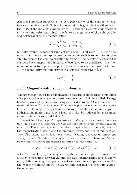
Figure 1.6: a) Schematic of a vertical spin-valve. Two FM layers are separated bya non magnetic interlayer. b) In the lateral geometry a non-magnetic medium is con-tacted from above by FM electrodes. c) Assuming that both FM are switching theirmagnetization at different switching fields HS, a reduction in the device conductancecan be seen when both FM are magnetized antiparallel.
this geometry is the possibility of contacting low-dimensional materials likemetallic strips [51], semiconducting nanowires [52], graphene [53] or CNTs[18, 19], and it is possible to create multiple terminals [51, 54].
The expected behavior for the spin-valve conductance in an external mag-netic field is illustrated in the lower part of fig. 1.6c. For simplicity, a sharpmagnetization reversal of the two FM contacts at the switching fields HS1
and HS2 is assumed as shown in the rectangular magnetization curves inthe upper graph. The conductance shows a hysteretic reduction when thecontacts switch from a parallel to an antiparallel configuration. The mag-netoresistance of the device is defined as7
MR =RAP −RP
RP=GP −GAP
GAP. (1.25)
1.2.4 Tunnel magnetoresistance
In general, a tunnel magnetoresistance (TMR) device consists of two FMcontacts separated by an insulator. The electron transport from one contact
7The term magnetoresistance is generally used in literature, also when measuringconductances [55]. Other definitions in use for the magnetoresistance are MR′ =GAP−GP
GPand MR′′ =
GP−GAPGP+GAP
.

14 Theoretical Background
to the other is dominated by tunneling through a barrier and the MR canamount to a few hundered percent at room temperature [56]. In the Jullieremodel [9] the transmission through the insulating interlayer is assumed in-dependent of the electron energy but proportional to the DOS at the Fermilevel EF of both contacts. Spin-flip processes at the interfaces and in theinterlayer are neglected.
The situation for parallel alignment of the FM layers is depicted in fig. 1.7aand is described in Mott’s two-current model [45]. A large amount of spin-up electrons (high DOS at EF) from one contact can tunnel into emptyspin-up states with a high DOS(EF) in the other contact, resulting in ahigh tunnelling current. For the spin-down electrons, the low DOS at theFermi level in both ferromagnets leads to a low tunnel current and thereforea higher resistance. For antiparallel alignment of the magnetizations thetunneling current for the spin-up electrons is decreased due to a smalleramount of empty up-spin states in the second FM, wheareas the current forthe spin-down states is increased as shown in fig. 1.7b. The total tunnellingcurrent is smaller in the antiparallel case where the low spin-up resistanceis dominating (see resistor schematic in fig. 1.7).
Using Fermi’s golden rule, the tunnelling current is proportional to theproduct of the density states Ni(EF) at the Fermi level for both electrodes(i = 1, 2) and the square of the tunnel matrix element M [57]. The tunnelmatrix element is assumed to be independent of energy for a small variationin the energy window between EF and EF − eV . The first order tunnelingcurrent then reads
I =2e
h|M|2
∫ ∞−∞
N1(E − eV )N2(E)[f(E − eV )− f(E)]dE (1.26)
with f(E) the Fermi function.
Assuming low temperatures and the DOS not varying much for smallapplied voltages V , the conductance in the parallel (P) and the antiparallel(AP) configuration is given by
GP = GP,↑ +GP,↓ ∼ N+1 N
+2 +N−1 N
−2 (1.27)
GAP = GAP,↑ +GAP,↓ ∼ N+1 N
−2 +N−1 N
+2 (1.28)
with G↑(↓) the conductance of the spin-up (spin-down) channel and N+(−)i
the DOS for electrode i = 1, 2 for majority (+) and minority (-) spin elec-trons. By inserting these expressions into the definition of the magnetore-sistance (eq. 1.25), a tunneling magnetoresistance in terms of the contact

1.2. Magnetoresistance effects in standard structures 15
E
EF
E E E
N1(E) N
1(E)
EF
R R
R R
a) b)
N2(E) N
2(E) N
2(E) N
2(E)
N1(E) N
1(E)
1 12 2
EF-eV E
F-eV
+ +- - + - - +
Figure 1.7: Schematic of the electron tunneling between two FM layers following theJulliere model. In a Stoner ferromagnet, the DOS of the 3d bands is spin-split atthe Fermi level which leads to a finite polarization of the charge carriers. The currentthrough the device is assumed to be independent of the electron energy but proportionalto the DOS. This leads to a smaller resistance of the device in a) the parallel than inb) the antiparallel configuration.
polarization P1 and P2 (eq. 1.14) is found
TMR =GP −GAP
GAP=
2P1P2
1− P1P2. (1.29)
Julliere’s model is a basic model that can help to understand basic features ofTMR devices. However, in experiments TMR values are found that cannotbe explained by this model (see Chapter 4). This is due to the fact that themodel does not include spin-flip effects in the barrier and at the interfaces.
1.2.5 Spin field-effect transistor
An example of a more complex spintronic device that allows modificationsof the magnetoresistance by control of the spin currents between two FMmaterials, the spin field-effect transistor (spin FET) has been envisionedby S. Datta and B. Das [58] in 1990 (see fig. 1.8). The spin polarizedcurrent is injected from an FM electrode into a low-dimensional channel, forexample provided by a two-dimensional electron gas (2DEG). The injectedelectrons move ballistically to the FM detector. In the moving frame of theelectrons the electric field of the gate is transformed partially to a magneticfield perpendicular to their moving direction. The moving electron spins will

16 Theoretical Background
precess about this magnetic field and are projected on the detector electrode.The underlaying spin-orbit interaction is called Rashba spin-orbit coupling[2] and has the largest effect in materials with large spin-orbit coupling [59].Modification of the gate voltage VG leads to different precession and differentcurrents detected in the FM detector.
VG
k
Ω
n
FM injector FM detector
2DEG
Figure 1.8: Schematic of the Datta-Das spin FET. A spin-polarized ballistic current isinjected and detected by two FM electrodes. The spin precession of the electrons aboutan effective magnetic field by the Rashba effect can be controlled by a gate voltage VG.
1.3 Carbon nanotube quantum dots
In this thesis we use carbon nanotubes (CNTs) as spin transport medium.One can imagine a CNT as a 2D hexagonal network of carbon atoms, asingle graphene sheet, that has been rolled up into a cylinder. These so-called single wall CNTs (SWCNTs) have a diameter on the order of a fewnanometers and a typical length in the micrometer range. SWCNTs can beeither metallic or semiconducting with varying band gap. The discovery ofSWCNTs was made by Sumio Iijima in 1993 [60], two years after its firstobservation of multi walled CNTs [13] (many concentric CNTs).
SWCNTs are often considered as prime examples of one-dimensional sys-tems [12]. The electron mean free path in CNTs is several µm long [61],up to 10µm [15]. When the mean free path exceeds the tube length, thetransport is ballistic. The carbon isotope 12C, making up 99 % of the carbonin CNTs, has no nuclear spin, making hyperfine interaction negligible. Inaddition, due to the low atomic number of carbon, spin-orbit interaction isweak. The length scale over which coherent spin transport is possible canbe 1µm [62]. This makes CNTs ideal media for spintronic devices.
1.3.1 Electronic properties of a graphene sheet
In a graphene sheet, every carbon atom has three nearest neighbors with aC-C bond length of a0 = 1.42 A. The unit cell, defined by the lattice vectors

1.3. Carbon nanotube quantum dots 17
a1 and a2, contains two carbon atoms and is shown in fig. 1.9a (shaded inorange). Graphene is sp2 hybridized. The (s, px, py) orbitals form strongcovalent σ bonds. These bonds determine the binding energy and the elasticproperties of the sheet. The pz orbitals form delocalized π (bonding) andπ∗ (antibonding) orbitals by overlap with their neighboring orbitals [14].
The dispersion relation can be calculated using a tight binding model[14, 63] taking only nearest neighbors into account and yields
E(k) = ±γ√
3 + 2 cos(ka1) + 2 cos(ka2) + 2 cos(k(a2 − a1)) (1.30)
with γ the overlap integral.The positive and negative solutions describe the π∗ and the π band, re-
spectively. A three dimensional plot of the energy dispersion relation isshown in fig. 1.9b. The two bands meet at six distinct points correspond-ing to the corners of the first Brillouin zone. Due to the symmetry of thehexagonal lattice, three out of the six points are equivalent. The two non-equivalent points are called K and K′. The energy dispersion is linear closeto the K-points. This is in contrast with the dispersion of more conventionalelectron systems (with parabolic bands).
The low energy properties can be described by a linear expansion of the
E
ky
EF
π*
π
kx
K K’
x
y
a1
a2
a0
a) b)
Figure 1.9: a) Schematic of the hexagonal structure of graphene. The unit cell definedby the lattice vectors a1 and a2 contains two carbon atoms. b) Three dimensional plotof the energy dispersion relation of graphene. The antibonding (π∗) and bonding (π)band form six valleys and meet at the six K-points corresponding to the corners of thefirst Brillouin zone.

18 Theoretical Background
wave functions around a K-point. With κ = k−K, the low energy dispersionrelation can be written as [63]
E(κ) = ±~vF |κ| (1.31)
with the Fermi velocity vF = 3γa0/2~ ≈ 106 m/s for γ = 3 eV [64].
1.3.2 Rolling up graphene into a nanotube
One can imagine a CNT as a slice of a graphene sheet rolled up into a cylinderto form a seamless tube. Regarding its electronic properties, the CNT canbehave either metallic or semiconducting. The geometrical structure of thetube depends on its circumferential or wrapping vector W = na1 + ma2
with n,m ∈ N as illustrated in fig. 1.10a. The orange shaded area in thefigure depicts the tube surface area. The translation vector T points parallelto the long axis of the nanotube.
armchair
zigzag
chiral
armchair (n,n)
zigzag (n,0)
W
T
(0,0)y
x
a1a2
a) b)
Figure 1.10: a) Schematic of the graphene honeycomb structure. The orange regiondefines an area that can be rolled up into a CNT. The wrapping vector W definesthe circumference of the tube. The vector T points along the tubes long axis. b)Different CNT structures result, depending on the wrapping vector. The illustrationshows armchair, zigzag and chiral type CNTs. The carbon atoms along the wrappingvector are highlighted red. (adapted from ref. [12, 65])

1.3. Carbon nanotube quantum dots 19
The tube diameter is found as
d =W
π=a
π
√n2 +m2 + nm (1.32)
with a =√
3a0 [12].
Depending on the indices (n,m) one can classify the CNTs into differentgroups. CNTs with wrapping indices (n, n) are called armchair tubes. Zigzagtubes are characterized by indices (n, 0). Tubes with arbitrary indices arechiral (see fig. 1.10b for illustration).
The wave functions in CNTs have to obey periodic boundary conditionsaround the circumference. The wave vector κ can be separated into onecomponent parallel (κ‖) and one perpendicular to the nanotube axis (k⊥).Because of the tube length of several micrometers (compared to a diameterof around one nanometer), κ‖ can be assumed continuous [65], whereas theallowed values of κ⊥ are restricted by
W · κ = πd κ⊥ = 2π(m− n
3+ p)
(1.33)
with p ∈ Z [63]. This quantization corresponds to cross sections in thegraphene band structure. If such a cross section contains K or K′, the tubeis metallic, i.e. has a finite DOS, while it has a band gap when it does not.The two situations are schematically shown in the plot of the energy cones
κ d
1
-1
2
-2
0 1 2-2 -1
p=2
p=1
p=3
semiconducting
1
0.5
1.5
-0.5
-1
-1.5
0-1-2 1 2
p=1
p=2
metallic
E
κx
κy
E
κx
κy
E E
κ d
a) b)
Figure 1.11: Low energy approximation of the graphene band structure (gray cones).Rolling up graphene: the quantization of the perpendicular component of the wavevector leads to subbands in the graphene band structure (light blue lines). a) Whenthe subbands do not include the origin (K-point) the tube is semiconducting. Thegraph shows a bandstructure plot of the first few bands closest to the K-point of asemiconducting (5, 0) nanotube. b) When the K-point is included, the CNT is metallic.In the graph the first bands of a metallic (6, 0) nanotube are plotted. The subbands areindicated with their index p

20 Theoretical Background
in fig. 1.11. Inserting eq. 1.33 into eq. 1.31 leads to the energy dispersionrelation [63]
E(κ‖) = ±2~vF
d
√(m− n3
+ p)2
+
(κ‖d
2
)2
. (1.34)
The energy dispersion only reaches zero for κ‖ = 0 for the subband with thenumber p, if (m−n)/3 = −p. Hence, all tubes with wrapping indices (n,m)obeying (m − n)/3 ∈ Z are metallic, the others are semiconducting. Twoexamples of dispersion relations of a semiconducting (5,0) and a metallic(6,0) tube are shown in figure 1.11. In addition, small band gaps can alsobe induced in metallic tubes with small diameter or by radial deformation[66].
1.3.3 Quantized transport in CNT quantum dots
In a quantum dot (QD) the electron wave functions are confined in three spa-tial directions to a size on the order of the Fermi wavelength. The energystates of this quasi zero-dimensional (0D) object take on only discrete val-ues. With this respect, QDs are comparable to atoms but have much largerdimensions and the charge carrier number can be tuned externally [67, 68].Electrical characterization of QDs is often done at cryogenic temperatures,where the single electron levels can be resolved. QD behavior can be foundfor example in metallic nanoparticles [69], molecules trapped between elec-trodes [70], self-assembled, lateral or vertical semiconductor nanostructures[71, 72], semiconducting nanowires [73], graphene [74] or CNTs [19].
A CNT can be considered as a one-dimensional conductor. By attachinga source (S) and a drain (D) contact, tunnel barriers form at the interfaces.This leads to the formation of a QD in the CNT (see fig. 1.12a). A highlydoped Si wafer, insulated from the CNT by a SiO2 layer can be used totune the energy levels of the dot. The coupling of the source (drain) contactis characterized by the capacitance CS(D) and the coupling strength ΓS(D).The backgate has the capacitance CG. This is depicted schematically infig. 1.12b.
The constant interaction (CI) model is a simplified model to describethis system [72, 75]. The first assumption made in the CI model is thatthe Coulomb interactions between the electrons on the dot and between theelectrons on dot and leads can be described by a single, constant capacitanceCΣ = CS + CD + CG. Furthermore, the single-particle energy spectrum isassumed independent of the number of electrons n on the dot. The energyspacing between the levels, also called orbital energy, is denoted as δE. To
add an electron to the QD, the charging energy UC = e2
CΣhas to be overcome.

1.3. Carbon nanotube quantum dots 21
backgate
S D
I
VSD
VG
quantumdot
Si
SiO2
metalQDS D
BG
CS ,Γ
SC
D ,Γ
D
CG
VG
VSD
a) b)
Figure 1.12: a) Side view of a CNT device: a quantum dot (QD) forms in the CNTbetween two metal contacts. The backgate can be used to tune the levels of the dot.The highly doped Si wafer used as a backgate is insulated from the CNT by a SiO2 layer.b) Schematic of the quantum dot capacitively coupled to a source (S) and a drain (D)contact. The coupling of the source (drain) to the dot is characterized by the couplingstrength ΓS(D) and the capacitance CS(D). The backgate is coupled with a capacitanceCG.
Typical charging energies for CNTs lie in the range 5−20 meV/L [15] whereL is the CNT dot length in µm.
Defect-free CNTs should show a four-fold degeneracy of the single-particlelevels. This four-fold degeneracy originates from the two-fold spin degener-acy and a two-fold subband degeneracy. Due to Coulomb interaction it coststhe charging energy UC to add electrons in the same level. When a level isfilled the next electron has to overcome the charging energy and the orbitalenergy, UC + δE. Four-fold patterns in the conductance are mostly visiblein clean CNTs with no perturbations or structural imperfections [76].
A schematic to explain electron transport in a QD in a simplified pic-ture can be seen in fig. 1.13. We assume that the electronic occupationof the leads is described by a Fermi function. At low temperatures, theFermi function changes to a step function where all electronic states up tothe electrochemical potential µ are filled, states above are empty. If theelectrochemical potential µQD of the QD is aligned with the electrochemicalpotentials of the source µS and the drain µD (fig. 1.13a) electron transportis possible. Otherwise transport is blocked (fig. 1.13b). The electrochemicalpotential of the QD can be tuned by an electrical gate. Another possibilityof tuning the quantum dot levels by the magneto Coulomb effect, introducedby ferromagnetic leads coupled to the QD, is discussed in chapter 4. Tuningthe electrochemical potential of the QD leads to an oscillating conductanceof the device, also called Coulomb oscillations.
In addition to the temperature broadening ∝ kBT , the energy levels of the

22 Theoretical Background
QD are broadenend due to life time broadening (Γ-broadening), described byLorentzian curves. The life time broadening is a consequence of the energy-time uncertainty principle ∆E ·∆t ≥ ~/2. The width of the energy level isinversely proportional to the time the electron stays on the dot. The fullwidth at half maximum (FWHM) of a lifetime broadened Coulomb peak isΓ = ΓS + ΓD [77].
Another possibility to overcome the Coulomb blockade is to apply a finitebias voltage VSD between S and D. This will lift the electrochemical potentialof the source to µS = µD − eVSD as shown in fig. 1.13c. Everytime a levelof the dot enters the energy window between µD and µS an additional con-ductance channel opens. To simplify the illustration of the measurementsone usually plots the differential conductance G = dI/dV . The differentialconductance shows a peak when a new level enters the energy window.
The lower graph in figure 1.13d is an example of a charge stability diagramof a CNT quantum dot. The red lines enclose the Coulomb diamonds, theregions where the transport is blocked and the number of electrons on thedot is constant. In the area around these Coulomb diamonds single-electrontunneling can occur. The Coulomb blockade peaks shown in the upper graphin figure 1.13d are the cross section of the Coulomb diamonds at VSD = 0 V.The stability diagram provides information about the charging energy andthe orbital energy of the dot. The charging energy UC can be read outdirectly from the height of a typical diamond and the height of every fourthdiamond displays the energy UC + δE. The diamonds can also be used tocalculate the lever arm η = eCG
CΣ= ∆VSD
∆VG(see fig. 1.13d) of the gate voltage.
For asymmetric capacitive coupling of the contacts the slopes β+ = |e| CGCS
on the left and β− = − |e| CGCΣ−CS
on the right side of the diamond will be
different and directly yield the source and drain capacitances [75]. The lever
arm can then be written as η =β+|β−|β++|β−| .

1.3. Carbon nanotube quantum dots 23
S
a)
µS µD
VSD
= 0
b)
µS µD
VSD
= 0
eVSD
c)
µS
µD
VSD
= 0
SD D DS
d)
VG
VG
VSD
G=dI/dV
0
UC+δE
ηUC
UC
UC+δE
n n+4
ΓS ΓD ΓS ΓD ΓS ΓD
η(UC+δE)
UC
∆VSD
∆VG
β+
β-
µQD
µQDµQD
Figure 1.13: a),b) Simplified schematic of the tunneling process through a quantumdot. When the electrochemical potential µQD of the QD is aligned with the electro-chemical potentials µS and µD of the source and drain contacts, tunneling can takeplace. The electrochemical potential of the QD can be tuned with a gate voltage. c)Applying a finite source-drain voltage opens an energy window between µS and µD.The dot will conduct when a dot level enters the energy window. d) Schematic repre-sentation of the differential conductance G = dI/dV (Coulomb blockade oscillations)and the corresponding stability diagram. The edges of the diamonds represent statesof high differential conductance. In the situation of symmetric capacitive coupling, the
lever arm of the backgate can be determined by η = eCGCΣ
=∆VSD∆VG
. In general, it is
calculated as η =β+|β−|β++|β−|
with β+(−) the left (right) slope of the diamonds.

24 Theoretical Background

Chapter 2Sample Fabrication and Measurements at
Cryogenic Temperatures
In this chapter we describe the carbon nanotube (CNT) growth by chem-ical vapor deposition and the device fabrication process. We discuss theelectrical contact to CNTs and introduce briefly the cryostats used for low-temperature measurements and the measurement set-up.
2.1 Wafer preparation
We use a highly boron doped Si wafer with a polished ∼ 400 nm thermallygrown SiO2 layer on top. The p-doped substrate has a resistivity of 10µΩcmand is used as a backgate. The oxide layer insulates the substrate from thedevice. Pieces of 1 x 1 cm2 are cut out of the wafer and cleaned in a bath-type sonicator in acetone for about one hour to remove dust from cuttingand organic residues on the surface. Then the substrate is sonificated for30 minutes in 2− propanol (IPA) to remove residues from the acetone andair blow dried. A 30 seconds reactive ion etch (RIE) is used to removesmall but persistent organic substances from the wafer surface. In the RIEhigh-energy ions from a chemically reactive oxygen plasma react with theresidues on the wafer surface [78]. The parameters of the process can befound in Appendix A. Alternatively, a 30 minutes UV ozone cleaning, adecomposition of the residues by UV light accompanied by an oxidation byfree oxygen radicals [79], is done.
25

26 Sample Fabrication and Measurements at Cryogenic Temperatures
2.2 Carbon nanotube growth
The CNTs used in the experiments are grown in-house in a chemical vapordeposition (CVD) system. A catalyst solution composed of iron nitrite seedparticles (Fe(NO3)3·9H2O), aluminum oxide (Al2O3) and MoO2Cl2 is spunon the substrate and heated up to 950C in a quartz tube in an argonatmosphere [80]. The exact composition of the catalyst solution is crucialfor the growth process [81, 82] and can be found together with the gas flowrates in appendix A. When the growth temperature is reached, the Ar gas isreplaced by methane (CH4) and hydrogen (H2) for 10 minutes. The methaneserves as feedstock gas and contains the carbon necessary for the nanotubegrowth. The carbon deposits on the catalyst particles and tube growth takesplace [12]. The hydrogen is needed to react with the excess carbon. Afterthe growth process the wafer is cooled down to room temperature in a Ar/H2
atmosphere. The growth process we use generates mainly individual singlewall CNTs with a typical length of 2-10 µm [81, 82].
a) b)catalyst clusters
individual CNTs
10 µm 5 µm
Figure 2.1: SEM images of a wafer with alignment markers and nanotubes after CVDgrowth. a) The catalyst solution has been sonicated in a bath-type sonicator for 3hours. Catalyst clusters on the surface are clearly visible. b) Sonicating the solution ina high-power sonicater prevents clusters on the wafer, leading to a better distributionof the CNTs on the surface.
It should be noted that the catalyst solution has to be treated with ul-trasonic to break-up catalyst nanoparticle clusters before it is spun on thewafer. Usually, this is done by placing a small glass container with the cat-alyst solution in a bath-type sonicator for ∼3 hours [81]. However, strongcatalyst clusters are often visible after the CNT growth, indicating thatbath-sonication is not sufficient to break-up all the clusters (fig. 2.1a). Goodresults were achieved by sonication of a small amount of catalyst solution ina high-power sonicater1 (see appendix A). An ideal distribution of individual
1Branson Digital Sonifier 450

2.3. Device fabrication 27
CNTs between four alignment markers can be seen in fig. 2.1b.
2.3 Device fabrication
A grid of alignment markers and the contact pads for bonding are fabricatedby electron beam (e-beam) lithography and metal deposition techniques afterthe CNT growth2. After the localization of the CNTs, two more fabricationsteps for the ferromagnetic and non-magnetic contact materials are done.
General fabrication process
The detailed fabrication process is shown schematically in fig. 2.2. Thecleaned wafer piece (fig. 2.2a) ist covered with an e-beam resist double layer(fig. 2.2b). For the double layer a 100 nm thick polymethyl methacrylat-methacrylic (PMMA/MA)3 layer is spin-coated on the wafer (4000 rpm, 40seconds) and baked on a hot plate at 200C for 3 minutes to evaporatethe solvents and harden the resist. In a second spin-coating process a 200nm thick polymethyl methacrylat (PMMA)4 layer is placed on top of thefirst layer and also hardened on the hot plate (200C, 3 minutes). Thelithographic patterning is done with a Zeiss SUPRA 40 scanning electronmicroscope (fig. 2.2c). The electron beam cuts the polymer chains of theresist in smaller pieces so that they can be removed in a developer bathconsisting of 1 part methyl isobutyl ketone (MIBK) and 3 parts IPA. Narrowlines can be structured in the PMMA layer using an acceleration voltage of 20kV with a 10 µm aperture (details about e-beam lithography parameters canbe found in appendix A). After the developing process, a metal is depositedin a Bestec evaporation system in ultra high vacuum (UHV) at a pressure< 5·10−10 mbar by thermal or electron beam evaporation (fig. 2.2d). Duringmetal evaporation the sample holder is cooled to -50C. This helps to reducethe heat load due to the deposited metal atoms and leads to a better lift-off.The walls of the UHV chamber are at -180C. After the metal depositionthe unexposed PMMA layer and the metal layer on top are removed in alift-off process in ∼50C warm acetone (fig. 2.2e). The fabricated sample(fig. 2.2f) is then rinsed with IPA and air blow dried.
2This is in contrast to ultra-clean fabrication methods where the CNTs are grownacross pre-formed contacts in the last fabrication step [83]
3AR-P 617 33 %, Allresist4AR-P 671.09 950 K, Allresist, diluted in chlorobenzene

28 Sample Fabrication and Measurements at Cryogenic Temperatures
a) b)
c) d)
e) f )
Si
SiO2
PMMA PMMA/MA
e-beam
acetone
metal
Figure 2.2: Schematic of the wafer processing. a) We start with a p-doped Si waferwith 400 nm SiO2. b)+c) A PMMA/MA - PMMA double layer is spun on the waferand then the polymer layer is structured with a scanning electron microscope. d) Afterthe development process, a metal layer is evaporated on the whole surface in a ultra highvacuum evaporation system. e) In a lift-off process in acetone the unexposed PMMAlayer is finally removed. f) The desired structure stays on the surface.
Contacting a CNT
This process is repeated several times: After CNT growth the alignmentmarkers and bond pads are structured and metallized with 40 nm Au ontop of 5 nm Ti. The Ti provides a good adhesion of the Au on the surface.
The wafer surface is then imaged with an SEM, using a low accelerationvoltage of 1 kV and a 30 µm aperture, to locate suitable nanotubes. SEMimaging provides a fast and simple possibility for CNT localization but it

2.3. Device fabrication 29
should be noted that the SEM is not imaging the geometrical contrast ofthe CNTs but the voltage contrast due to a different backscattering of theelectrons in the area where the CNT is located [84]. The CNTs appear muchlarger than their actual geometrical size. To obtain information about thetube radius we are using an atomic force microscope (AFM). A disadvantageof the SEM is that observations can damage the nanotubes or generatecarbonaceous coating [85]. To reduce SEM induced defects, we keep theexposure time of the CNTs as short as possible.
After localization the sample is covered with the polymer double layeragain for further structuring. The alignment grid allows us to contact aCNT with an accuracy of < 10 nm. Before the ferromagnetic contacts aredeposited, the sample is heated in the load-lock of the evaporation systemwith a heat lamp (< 200C, 60 min.) to remove water in the contact area.Surface-bound water molecules close to the CNT can lead to contactingproblems and charge traps responsible for instabilities found in electronictransport measurements [86].
After the deposition of 25 nm Permalloy, our material of choice for theFM contacts (see chapter 3), a third SEM structuring step is done for theleads connecting the FM contacts with the bond pads. To remove the ox-idized layer on top of the FM contacts, we sputter the contact areas for 2
500 µm
60 µm
2 µm
Pd
SiO2
Py
CNT
marker
Figure 2.3: The image on the upper left shows a device glued in a chip carrier with anedge length of 8 mm. The Au pads on the device are bonded to the contact pads of thecarrier by Al wires. In the zoom-ins shown in the lower SEM images one can see how aCNT is contacted with Py strips.

30 Sample Fabrication and Measurements at Cryogenic Temperatures
minutes with an Ar sputter gun (in the load-lock of the evaporation system,details can be found in appendix A). Then 50 nm Pd is deposited connect-ing the Permalloy strips with the bonding pads. (In some devices the Pd isevaporated in the second step and the FM material in the last step)
The finished device is cut to a size of 5 x 5 mm2 and glued into a chipcarrier with silver paint. The gluing with the conducting paint allows toelectronically connect a cleaved edge of the Si wafer which provides a back-gate.
A complete device is depicted in fig. 2.3. The optical image in the upperleft corner shows a wafer piece glued into a chip carrier. 18 Au bond padsare bonded with a 32 µm thick Al wire to the chip carrier. The zoom-ins show SEM images of the device. The bond pads provide contacts to 2marker fields on the wafer (yellow rectangular). In the orange rectangular,one marker field is shown in detail. Inside the red rectangular a 6 µm longCNT can be seen that is contacted by two Py electrodes. Both electrodesare contacted from both sides with non-magnetic Pd to be able to measurea magnetoresistance signal through the FM strip (see chapter 3).
Double layer e-beam resist
The above introduced resist double layer is used to obtain good metal lift-off. When only PMMA is used as a resist it is sometimes problematic toremove the metal layer completely from the wafer surface and, especially insmall structures, the edges are sometimes not well defined.
In fig. 2.4a two alignment markers written with the same parameters arecompared. The marker in the upper SEM image is fabricated using a singlePMMA layer, whereas a PMMA/MA-PMMA double layer is used for themarker in the lower image. The edges of the marker fabricated with thedouble polymer layer are much better resolved.
The PMMA/MA layer below gives a deeper undercut with the same writ-ing parameters due to the shorter polymer chain length and can easier bedesolved in the developing step. In fig. 2.4b we show a cross section of awafer covered with the PMMA/MA-PMMA double layer. A 500 nm wideline has been written with an electron beam and metalized with Permalloy(Py) after development. The wafer has then been dipped into liquid nitrogenand was cleaved subsequent with the polymer layer on top. This allows toobtain a sharp breaking edge without a deformation of the polymer duringthe cleavage. The white dotted line marks the threshold between the twopolymer layers. In the zoom-in in the right image an undercut of ∼100 nmon each side of the 500 nm wide strip is visible in the PMMA/MA layer.

2.4. Improving the electrical contact to CNTs 31
500 nm
SiO2
Si
PyPMMA/MA
PMMA
100 nm 100 nm
500 nm
a) b)
Figure 2.4: a) SEM images of an alignment marker structured with a PMMA layer(upper image) and a PMMA/MA-PMMA double layer (lower image). The edges of themarker structured with the polymer double layer are better defined. The scale bars havea length of 1 µm. b) SEM image of a 500 nm wide line written in a PMMA/MA-PMMAdouble layer after developing and metal deposition. The right image shows a zoom-inof the image on the left. A clear undercut of around 100 nm on each side of the metalstrip can be seen in the PMMA/MA layer.
2.4 Improving the electrical contact to CNTs
Contacting carbon nanotubes with metallic contacts is a rather complexsubject. It is theoretically predicted that the charge transport in a CNTcan be controlled by Schottky barriers forming at the interfaces between theCNT and the metallic contacts and the device characteristics are stronglyinfluenced by the work function of the metal contact [87]. It was also shownon basis of calculations that the numbers of chemical bonds (the wettingof the material) and the height of the Schottky barrier are related [88].The models show that Pd provides chemical bonds to the delocalized π-like system of the CNT and therefore shows a good wetting of the CNT.Furthermore, the work function of Pd matches very well the work functionof the CNT [89]. The good electrical contacts of Pd to CNTs has also beendemonstated experimentally [90]. However, the states of these two modelsdo not apply to all metals.
Residuing polymer layers
Great effort has already been undertaken by different research groups to ex-perimentally investigate the electrical contact to CNTs of both non-magnetic[90] and ferromagnetic metals [91]. In chapter 3 we study the contact char-acteristics of several metals to CNTs. It was found that the ferromagneticPermalloy (with a work function comparable to Pd [92]) made low ohmicelectrical contact to CNTs in the first two batches of samples. However, thelow contact resistances could not be reproduced in later devices.

32 Sample Fabrication and Measurements at Cryogenic Temperatures
0.0 0.5 1.0 1.5 2.0
h (n
m)
x (µm)
0
10
20
30
40
50
400 nm0
10
20
30
40
50
h (nm)
0.0 0.2 0.4 0.6 0.8 1.0 1.2
x (µm)
h (n
m)
0
1
2
3
4
5
6h (nm)
0
4
8
10
12
400 nm
a)
b)
5 nm
25 nm
15 nm
5 nm
0.1 µm
Figure 2.5: a) AFM image of two 25 nm high Py strip showing residues on both sidesclose to the contacts. These residues are not conducting and cannot be removed instandard RIE processes. On the right side the corresponding line graph is shown. Closeto the contacts steps of ∼ 5 nm are visible. On top ∼ 15 nm high steps are found. b)Also in areas where the PMMA has been structured and developed but not metalizedbefore the lift-off process polymer residues with a typical height of 5 nm are found.
By investigating our Permalloy contacts with AFM and SEM we foundlarge scale residues close to the contact. In fig. 2.5a an AFM image of two200 nm and 400 nm wide Permalloy strips is shown. The thickness of thedeposited material is 25 nm. Residues on both sides of and most likely belowthe metal strips can clearly be seen. A line cut, indicated by the yellow line,is shown on the right. Steps of ∼ 5 nm height close to the contacts are visible.It seems that the 25 nm thick metal strips are positioned on plateaus. Ontop, 15 nm high steps are visible. We found that the residues close to thecontacts are not conducting and cannot be removed in the standard RIEprocess used for wafer cleaning. The residuing layers close to the contactsare also visible by SEM imaging with a good contrast (see appendix B).We find that the residues are independent of the used area exposure dose,

2.4. Improving the electrical contact to CNTs 33
still visible for very high and very low doses. The AFM image in fig. 2.5bshows an e-beam structured and developed region where no metal has beendeposited before the lift-off process was done. PMMA residues of ∼ 5 nmheight are visible, clearly showing the outline of the proposed strip shape.
In the literature, several studies report a residual resist polymer layer of 2-5 nm that stays on the surface after the development process [93, 94, 95, 96].We think that PMMA residues that are not removed completely in thedevelopment process, are metallized with Permalloy during the evaporationprocess and oxidize when exposed to air later. For other evaporated metalswe do not see such features which is probably due to a higher diffusion ofPermalloy on the surface. A polymer layer in between the CNT and themetallic contact will lead to very high and unreliable contact resistances.The standard procedure in literature to remove the residuing polymer layeris an oxygen plasma cleaning [94], however this process is not possible forus because it damages or removes our nanotubes.
To reduce the resist residues we studied the effect of different baking timesand temperatures on the hot plate, and additional treatments of the PMMAlayer like UVO or RIE treatments before metal evaporation. Details of thestudies and the corresponding SEM images can be found in appendix B. Theresults are that neither the baking temperature nor the baking time have asignificant influence on the polymer residues or the electrical contact. Bychanging the baking procedure it is not possible to dispose of the residuinglayer. A different approach to solve the residue problem is presented below.
Electrical stability of the devices
Another problem with a probably related cause is the electrical stability ofthe fabricated devices. The electrical stability can be influenced by chargerearrangements in the electrical device due to trapped charges in the SiO2
layer, at the SiO2/Si interface [97] or in water molecules bound to the nan-otube [86]. We found an indication of remaining resist when we investigatedour CNTs after a structuring process that can perhaps also lead to trappedcharges close to the device. Fig. 2.6a shows an SEM image of a CNT afterevaporation of the alignment markers. Irregularities on the nanotube with atypical diameter of 30 nm and separated by ∼ 200 nm are visible. The imageon the right shows a part of the CNT imaged with a higher resolution. Theresidues can also be seen by AFM imaging. Fig. 2.6b provides a comparisonof residues on two crossed CNTs imaged with AFM (left image) and SEM(right image). The residues are visible in both images. We think that theseresidues are polymer clumps sticking to the nanotubes that are not resolvedin acetone.
The only definite way to avoid this kind of contamination is to grow the

34 Sample Fabrication and Measurements at Cryogenic Temperatures
400 nmPMMA residues200 nm
a)
b)
Figure 2.6: a) SEM image of a CNT after the alignment marker processing step. Itseems that polymer residues remain after metal lift-off and can contaminate the nan-otube. The image on the right is an SEM image taken with a higher resolution. b) Theresidues on a crossed CNT device are visible in AFM images (left side) and SEM images(right side). The images of the crossed CNT device are kindly provided by AndreasWepf.
CNTs in the last step on the prefabricated contacts. With this fabricationprocess, ultraclean nanotube devices can be obtained [83, 98]. However,for our devices we need narrow ferromagnetic contacts with well defined di-mensions (see chapter 3) and melting or deformation of the metals on thewafer surface when heated to CNT growth temperatures of over 900C canbe problematic. Additionally, the fabrication of multiterminal structures re-quires considerable more effort because CNTs have to bridge several contactsby accidentally falling in the right orientation.
To solve the problem of the remaining polymer residues we started totake another approach in sample fabrication. After the CVD growth ofthe nanotubes we deposit 5 nm Al2O3 on the wafer surface by atomic layerdeposition (ALD) in an accurately controlled process. Thereby it is crucialthat the deposited layer is homogeneous. After the deposition, the sample iscovered with PMMA and alignment markes are structured and metallized.We found that CNTs can still be located below a thin layer of Al2O3. Before

2.5. Measurement set-up 35
the contacts to the CNT are metallized the sample is dipped for 30 secondsinto 25 % tetramethylammonium hydroxide (TMAH) dissolved in water (T =50C). TMAH is a strong base generally used for Al, Al2O3 or Si etching [99].The etching removes the oxide from the contact layer but does not affect thenanotube itself or the surrounding PMMA. The process is stopped in H2O.Cleaning the sample in the UVO system before the TMAH etching helps toimprove the removal of the oxide. With this additional fabrication step it ispossible to deposite metallic contacts on CNTs without ever bringing themin contact with resist. Additional information to the process is provided inappendix B.
2.5 Measurement set-up
We first test the sample at room temperature with a needle prober or in adipstick with a sample test box. An AC voltage of 1 mV is applied betweenthe two contacts and the current through the device is measured with alock-in amplifier5. This allows for a quick functionality test of the deviceand yields information about the contact resistances and a metallic or semi-conducting behavior of the CNT. When the CNT device is conducting it istransfered to a cryostat and cooled down.
Resolving the single electron levels of a quantum dot is not possible atroom temperature. Measurements of single energy levels in a quantum dotrequire cryogenic temperatures and a good filtering of the electrical leadsto minimize high frequency noise and heating effects. In the cryostats RLClow pass filters (tape worm filters) made of twisted Isotan (CuNi) wireswrapped in a Cu band are used for filtering (attenuation: 60 dB at 1 GHz, dcresistance 64 Ω [100]). They are built by the in-house electronics workshopof the University of Basel. At room temperature low-pass π-filters are usedto filter out high frequency noise (attenuation: 40-60 dB for frequencieshigher than 0.3 MHz [101]).
A schematic of the measurement set-up can be seen in fig 2.7. For con-ductance measurements an AC signal VAC with a frequency of 77.77 Hz isgenerated by a lock-in amplifier. This AC signal is superimposed on a DCbias voltage VSD by a transformer (transformation ratio 4:1). Often, theDC signal is generated with a DC auxiliary output of the lock-in ampli-fier. A voltage divider scales resulting voltage down by a factor 1000. At230 mK, a typical voltage applied to the device is VAC = 10 µV. This islow enough to prevent thermal broadening of the energy levels in the dot(eVAC < kBT ≈ 20µeV). The current in the device is converted to a voltage
5Stanford Research Systems SR 830 DSP

36 Sample Fabrication and Measurements at Cryogenic Temperatures
π-filter
rf-filter
T = 230 mK
room temperature
DC source
10 kΩ
10 Ω
1 MΩ
GPIB
source
drain
backgate
DC sourceLock-In
AC signal
- +
RIV-converterratio: 107-109 Ω
voltagedevider1:1000
transformer1:4
securityresistor
Figure 2.7: Schematic drawing of a typical measurement setup.
by an I/V converter with a conversion ratio of 107 − 109 Ω. This voltage isthen detected with the lock-in amplifier.
The backgate voltage VBG, used to tune the energy levels of the QD, is

2.6. Cryogenics 37
generated with an external voltage source6. A resistor in the current pathis used to prevent high currents on the device in case of backgate leakage.All instruments are controlled via GPIB by LabVIEW programs7.
2.6 Cryogenics
In this thesis mainly two cryostats are used. A schematic of a 4He cryo-stat is shown in figure 2.8a. The variable temperature insert (VTI) allowsfast device measurements and continuous runs up to 300 K. The sample inkept in a vacuum chamber dipped into liquid Helium (THe = 4.2 K, drawnin light blue). Through a needle valve, He is sucked into the insert lower-ing the temperature inside further due to evaporation cooling. The loweststable temperature we reach with this system is around 1.7 K. The He stor-age is shielded from the warmer environment by the inner vacuum chamber(IVC). The vacuum minimizes thermal coupling to the outer parts of thecryostat. To minimize heating by radiation a metal shield cooled by liquid
6Yokogawa YK 76517LabVIEW 6.1 by National Instruments
N N
He
pump
shields
needle valve
magnet
OVC
IVC
1K pot
3He
sample
sorb
a) b)
VTI
sample
Figure 2.8: a) Schematics of a 4He cryostat. In the VTI 4He is evaporated througha needle valve to reach temperatures of around 1.7 K. b) Working principle of a 3Hecryostat. 3He is evaporated in a close circuit to reach temperatures down to 230 mK.

38 Sample Fabrication and Measurements at Cryogenic Temperatures
nitrogen (dark blue) surrounds the He storage. The nitrogen shield is ther-mally decoupled from the outside by an outer vacuum chamber (OVC). Asuperconducting magnet in the He bath allows the application of magneticfields up to 8 T.
If temperatures below 1 K are needed a 3He cryostat is used. The basicworking principle is shown in figure 2.8b. 3He is a helium isotope with ahigher vapor pressure than 4He [102]. Therefore, the cooling power of 3Heis higher at low temperatures. However, 3He does not occur in nature inlarge quantities and is rather expensive. It is usually stored only in smallquantities. A closed 3He cycle shielded by a 4He bath is used to reachtemperatures around 230 mK. Liquid 3He is evaporated in a chamber inthermal contact with the sample and collected in a charcoal sorbtion pump(sorb). In order to condense the 3He, the sorb has to be heated to 30 K torelease the 3He gas (heating lines are drawn in yellow). The 3He gas thencondenses in the 1K pot (T = 1.5 K), cooled by controlled evaporation of4He and collects again in the chamber above the sample. The cooling to verylow temperatures is thus limited to a few days before all 3He is evaporatedand the cycle has to be restarted by heating the sorb. The 3He cryostatcontains a superconducting magnet with a maximum field of 8 T.

Chapter 3Ferromagnetic Materials for Carbon
Nanotube Spintronic Devices
Considerable effort is dedicated to use carbon nanotubes for spintronic ap-plications [19, 62, 103, 104]. In CNT devices a ferromagnetic metal, likeNiPd [19, 104], Co [18, 54] or various others [105, 106, 107] is used to injecta spin polarized current into the CNT. However, for many materials thelocal magnetization at the contact area and the contact resistance to carbonnanostructures were found to be of poor reproducibility. Some also developan out-of-plane magnetization and multidomain structures, leading to largestray fields at the devices and unreliable MR behavior. For this reason, oneof the main goals of this thesis was to find an FM material that fulfills thedesired requirements and to optimize the relevant properties. Ideally, thefollowing requirements have to be met by the ferromagnetic material in aCNT spin-valve:
1. A large spin polarization: to obtain a large spin signal
2. The shape anisotropy dominates the crystal anisotropy : to allow tuningof the switching fields by the contact geometry.
3. A single magnetic domain covering each contact area: to avoid thecompensation of the spin injection by neighboring domains. In theideal case the whole contact consist of a single domain which allowsto relate directly the MR signal with the magnetization reversal of thecontact observed in AMR signals of individual strips.
39
40 Ferromagnetic Materials for Carbon Nanotube Spintronic Devices
4. In-plane magnetization: to reduce stray fields on the CNT.
5. Reproducible electronic coupling to the medium between the contacts:to allow reproducible fabrication of devices and high yields.
In this thesis, a series of materials were considered and tested. We presentin this chapter the results on different ferromagnetic materials and discusstheir properties with respect to the above points. We demonstrate thatPermalloy (Py), a widely used Ni/Fe alloy, meets the requirements for theinjection and detection of spin polarized currents in carbon nanotube spin-tronic devices. We establish the material quality and magnetization proper-ties of Py strips in the shape of suitable electrical contacts and find a sharpmagnetization switching tunable by geometry in the anisotropic magnetore-sistance of a single strip at cryogenic temperatures. In addition, we showthat Py contacts couple strongly to CNTs, thereby forming quantum dotsat low temperatures1.
The FM contacts studied in this thesis are cuboids with a typical lengthof 10 − 17µm. They are contacted with Pd leads for electrical transportmeasurements. This is in contrast to structures completely fabricated of anFM material (like e.g. [109]) and minimizes stray fields on the device. Theelongated shape allows to minimize stray field effects on the CNT due tothe end domains of the contacts.
3.1 Methods of investigation
To investigate the magnetic properties of the tested materials, differentmethods were used. The vibrating sample magnetometer (VSM) allows fora quick quality check of the evaporated material at room temperature. Forstudies of the magnetic behavior of individual FM strips we make use ofanisotropic magnetoresistance (AMR) measurements at low temperatures.
3.1.1 Vibrating sample magnetometer
The quality of an evaporated ferromagnetic thin film can be tested witha VSM. The wafer with the FM film is placed inside a uniform magneticfield (Hmax = 2 T in our system2) as shown in fig 3.1a. This leads to amagnetization of the FM material. The sample is then vibrated sinusoidallyup and down, leading to a sinusoidal variation of the magnetic flux throughseveral nearby pickup coils. The variation of the flux induces a voltage inthe coils, proportional to the magnetic moment of the sample [110]. The
1Parts of this work have been published in [108]2LakeShore VSM 4700

3.1. Methods of investigation 41
magnetic eldsample
pickup coils
U
Ia) b)
H3 µm
1
2 3
4FM wirew
magnetic fielddue to M
Figure 3.1: a) Schematic of a VSM. The sample is vibrated sinusoidally in a uniformmagnetic field. The variation in magnetic flux is detected by pickup coils. b) False-colorSEM image of an FM strip with width w contacted in a 4-terminal geometry for AMRmeasurements.
comparison of the measured saturation magnetization and the coercive fieldof the thin film can then be compared to literature values.
We also use the VSM to gain information about the magnetization andthe switching fields of fabricated contacts. However, the magnetic momentof a single 300 nm wide strip is ∼ 6 · 10−5 µemu, far below the sensitivity ofthe system (noise floor 0.1µemu). We therefore investigate strip grids with∼170,000 parallel strips with a total magnetic moments of ∼ 10µemu. Wevary the number of investigated strips in these strip grids for different widthw to keep the total volume of material constant. One has to keep in mindthat the signal can differ from the signal of an individual contact due to FMstray field interactions between the strips and other effect (see below).
3.1.2 Anisotropic magnetoresistance
Due to spin-orbit interactions, the electrical resistance in a ferromagneticmetal depends on the relative orientation of the magnetization and the cur-rent direction (see chapter 1). We use the AMR to investigate an individualcontact strip in a four-terminal geometry at low temperatures. In this geom-etry, the device resistance is measured without the additional componentsof the cable resistances, the lead resistances and the contact resistances. Afalse-color SEM image of a typical device can be seen in fig. 3.1b. A 12 µmlong FM strip of width w (red) is contacted with four Pd contacts (gray). Acurrent is injected from contact 1 to 4 and the voltage drop over the contacts2 and 3 is measured. At the same time an external magnetic field, applied
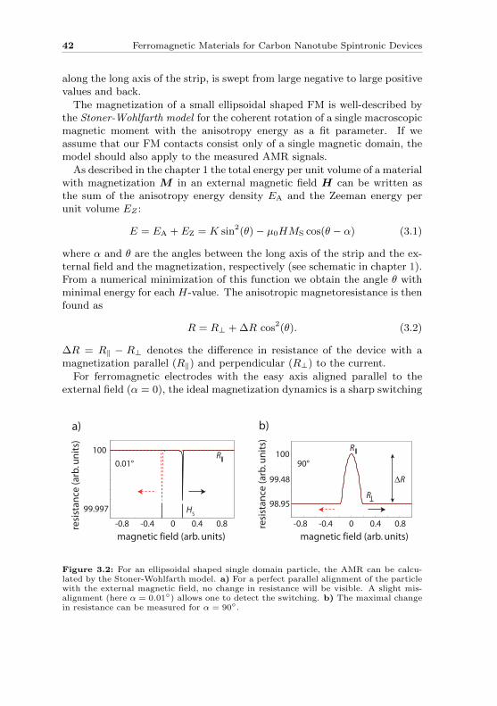
42 Ferromagnetic Materials for Carbon Nanotube Spintronic Devices
along the long axis of the strip, is swept from large negative to large positivevalues and back.
The magnetization of a small ellipsoidal shaped FM is well-described bythe Stoner-Wohlfarth model for the coherent rotation of a single macroscopicmagnetic moment with the anisotropy energy as a fit parameter. If weassume that our FM contacts consist only of a single magnetic domain, themodel should also apply to the measured AMR signals.
As described in the chapter 1 the total energy per unit volume of a materialwith magnetization M in an external magnetic field H can be written asthe sum of the anisotropy energy density EA and the Zeeman energy perunit volume EZ :
E = EA + EZ = K sin2(θ)− µ0HMS cos(θ − α) (3.1)
where α and θ are the angles between the long axis of the strip and the ex-ternal field and the magnetization, respectively (see schematic in chapter 1).From a numerical minimization of this function we obtain the angle θ withminimal energy for each H-value. The anisotropic magnetoresistance is thenfound as
R = R⊥ + ∆R cos2(θ). (3.2)
∆R = R‖ − R⊥ denotes the difference in resistance of the device with amagnetization parallel (R‖) and perpendicular (R⊥) to the current.
For ferromagnetic electrodes with the easy axis aligned parallel to theexternal field (α = 0), the ideal magnetization dynamics is a sharp switching
-0.8 -0.4 0 0.4 0.8
magnetic field (arb. units)
resi
stan
ce (a
rb. u
nit
s)
100
99.997
magnetic field (arb. units)-0.8 -0.4 0 0.4 0.8re
sist
ance
(arb
. un
its)
100
98.95
99.48
0.01° 90°
a) b)
HS
RR
R
∆R
Figure 3.2: For an ellipsoidal shaped single domain particle, the AMR can be calcu-lated by the Stoner-Wohlfarth model. a) For a perfect parallel alignment of the particlewith the external magnetic field, no change in resistance will be visible. A slight mis-alignment (here α = 0.01) allows one to detect the switching. b) The maximal changein resistance can be measured for α = 90.

3.2. Ferromagnetic Materials 43
by 180 at the switching field HS without prior rotation and formationof multiple domains when the magnetic field is reversed. In this case novariation of the AMR is expected. A detectable signal can be achievedin this configuration with a slight misalignment (≤ 2), as shown in theexample in fig. 3.2a for α = 0.01. One finds a clear discontinuous changein the resistance and a very sharp switching.
The maximal change in resistance ∆R can be obtained by applying thefield perpendicular to the electrode (α = 90). An example of the expectedcurve for an ellipsoidal shaped single domain particle is shown in fig. 3.2b.
The AMR studies allow to study the magnetization reversal of a contactand to draw conclusion about possible multiple domains.
3.2 Ferromagnetic Materials
We first discuss the suitability of the 3d transition metals Ni, Co and Feas contact materials for CNTs. Then we present our results on the FMalloys PdNi, PdFe and NiFe. Extensive results are only shown on the lattermaterial.
3.2.1 Ni
Due to its good contact properties to CNTs, the soft ferromagnet Ni isused in different groups for spin transport experiments in nanotubes [11,111]. The crystal anisotropy is small compared to the shape anisotropy(4 · 10−3 J/cm3 and 7 · 10−2 J/cm3, respectively [112]) and the easy magne-tization axis of cylindrical wires is well aligned with their long axis up toa wire diameter of 60 nm [112]. For thicker diameters the easy axis has acomponent pointing out of the wire and the magnetization reversal is ac-companied by a curled domains formation. The average domain size for a45 nm thin Ni film is ∼ 275 nm with domain walls between 20 and 60 nmwidth [113]. The values determined for thin films are smaller than for singlecrystal bulk materials due to the additional component of a surface magne-tocrystalline anisotropy. The domain size is scaling with the square root ofthe film thickness.
To study the magnetic behavior of individual Ni strips in external mag-netic fields, we investigated the 4-terminal AMR of several 50 nm thick stripsat 1.6 K. Fig. 3.3a shows the resistance of a 1500µm long and 100µm wide,thermally evaporated Ni strip in an external magnetic field applied parallelto the strip axis. A gradually decrease in resistance is investigated for adecreasing magnetic field, starting at +0.2 T. A similar behavior is foundfor the up-sweep of the field. Sharp switching features are not observed.A gradually changing resistance can also be seen in fig. 3.3b for a 15µm

44 Ferromagnetic Materials for Carbon Nanotube Spintronic Devices
Ni
a)
-0.2 -0.1 0.0 0.1 0.2159.0
160.0
161.0
162.0
µ0H (T)
R (Ω
)
b)
Ni
16.3
16.4
16.5
16.6
R (Ω
)
-0.2 -0.1 0.0 0.1 0.2
µ0H (T)
Figure 3.3: a) 4-terminal AMR signal of a 50 nm thick Ni strip with a lenght ofl = 1500µm and a width of 100µm in an external magnetic field applied along thelong axis of the strip. No sharp switching features are visible, only a gradual changein resistance with the external magnetic field. b) The AMR of a 100 nm wide Ni strip(d = 50 nm, l = 15µm) shows the same characteristic behavior as the bigger strip shownin a).
long and 100 nm wide electrode with the same film thickness in a parallelmagnetic field. We assume that this gradual change in the AMR, that al-ready starts before the external magnetic field reaches zero, goes back toa formation of multiple domains in the Ni strip and an easy axis not wellaligned with the long axis of the strip, in agreement with results for thecylindrical geometries [112]. This not well defined switching behavior makesNi contacts not useful for our purpose.
3.2.2 Co
In Co nanowires the magnetocrystalline anisotropy is roughly the same sizeas the shape anisotropy (4.5 · 10−1 J/cm3 and 6 · 10−1 J/cm3, respectively[112]). However, for nanowires with diameters smaller than 40 nm a singledomain state with an easy axis along the nanowire long axis is observed[112, 114]. The domain size in 50 nm thick films is around 100 nm, almostthree times smaller than for Ni [112].
Block-shaped strips made of Co are used by different groups for spintransport experiments [18, 54, 103, 115]. The magnetization in these stripsshows sharp switching features and the switching field can be tuned by thewidth of the strips.
AMR measurements of 35 nm thick Co strips can be seen in fig. 3.4. Thegeometries of the strips are comparable to the Ni strips discussed above(fig. 3.4a 1500µm x 100µm, fig. 3.4b 15µm x 100 nm). The large Co stripshows a much sharper resistance change with less rotation compared to the

3.2. Ferromagnetic Materials 45
Co
a)
-0.2 -0.1 0.0 0.1 0.2
0.04
0.02
0.00
µ0H (T)
∆R (Ω
)
Co
b)
28.80
28.86
28.92
28.98
-0.2 -0.1 0.0 0.1 0.2
µ0H (T)
R (Ω
)
Figure 3.4: a) 4-terminal AMR signal of a 35 nm thick Co strip with a length of1500µm and a width of 100µm. b) 2-terminal AMR signal of a 100 nm wide Ni stripwith a length of 15µm and 35 nm thickness. Sharp switching features are visible asrequired.
Ni strip of similar dimensions. This becomes even more pronounced for thenarrow strip. The (2-terminal) AMR of the narrow strip shows the desiredbehavior: a slight decrease in resistance before a sharp switching featureis visible. However, the contact properties of Co to CNTs are found to berather poor. Contacting CNTs is not very reproducible and the contactswere found to freeze out at low temperatures [116].
3.2.3 Fe
Only few magnetotransport experiments have been done with Fe contacts(e.g. [105]). Fe is believed to suffer from a high oxidation rate and wasexpected to give poor results. To confirm this, we first evaporated Fe filmson wafers to study their oxidation behavior with X-ray photoelectron spec-troscopy (XPS). 3 pieces of Si wafer were etched in hydrofluoric (HF) acid(40 %, 4 min.) to remove the silicon oxide layer on the surface. This wasdone to make sure that an oxygen signal measured by XPS cannot be due tothe SiO2 layer. After etching, the wafer pieces were immediately mounted inthe evaporation system for metal deposition, where 40 nm Fe were deposited.
The first piece was brought directly from the evaporation system to theXPS system and mounted in the vacuum chamber. It has been exposedto air for around 2 minutes. In a first scan we found O, N and C on thesurface. We also found the Fe 2p3/2 peak shifted to iron oxide position ataround 711.0 eV [117]. After 5 minutes Ar sputtering of the sample (2.5kV, 7 · 10−5 mbar) we have not seen N and C anymore. Some small amountof O could still be found. However, the Fe 2p3/2 peak was now found at

46 Ferromagnetic Materials for Carbon Nanotube Spintronic Devices
740 730 720 710 700
0.0
0.2
0.4
0.6
0.8
1.0 Fe 2 min in air Fe 1 h in air Fe 3.5 h in air
inte
nsity
(a.u
.)
binding energy (eV)
706.8 eV
730 720 710 700
0.25
0.50
0.75
1.00 Fe after Ar-sputtering Fe before Ar-sputtering
inte
nsity
(a.u
.)
binding energy (eV)
706.8 eV
711.0 eV
Fe 2p1/2
Fe 2p3/2
Fe 2p1/2 Fe 2p
3/2
a) b)
Figure 3.5: a) XPS measurement on an Fe film that has been exposed to air for around2 minutes (red line). The peaks for pure Fe are shifted to the Fe oxide position. AfterAr sputtering the pure Fe peaks are found again (black line). b) Photoelectron signalintensity of three Fe films oxidized for 2 min, 1 h and 3.5 h in air after 5 min of Arsputtering. Pure Fe is found below an oxidized layer independent on the oxidation time.
its elementary position (706.8 eV) as can be seen in fig. 3.5a. The secondand third sample have been oxidized in air for 1 h and 3.5 h, respectively.For both we saw an Fe oxide peak before sputtering and the elementary Fepeak after sputtering for 5 minutes. The Fe peak position for the differentsamples are shown in fig. 3.5b. The longer oxidation time does not lead to achange in the photoelectron signal intensity of the three samples. A longersputtering (10 minutes) does not change the result. The sputtering rate forFe was determined at the edge of the sample to be 1 nm per minute. Weconclude from these experiments that the Fe film is not oxidized completely.It oxidizes fast on its surface when exposed to air. However, after removingof 5-10 nm of the top layer we see essentially pure iron.
For a first study of the magnetic properties of our Fe films we did a roomtemperature vibrating sample magnetometer (VSM) characterization at theInstitut fur Physik in Karlsruhe3. Several 40 nm thick Fe films have beenexposed to air for around 4 h. A VSM magnetization measurement of afilm is plotted in red in fig. 3.6a. The saturation magnetizations of thefilms was found ∼ 1750 (±100) emu/cm3 when we assume that 5 nm Fe onthe surface are oxidized and do not contribute to the total magnetization.This value is in good agreement with the value for bulk Fe (1714 emu/cm3
[20]). The Fe layer shows a sharp change in magnetization at the coercivefield field of 8 mT. The additional step that is visible between 8 and 30 mTcan be traced to a diagonally cut edge (see schematic in the inset) that
3collaboration with Dr. C. Surgers

3.2. Ferromagnetic Materials 47
-40 -20 0 20 40
-1.0
-0.5
0.0
0.5
1.0
4 months 4 hours
µ0H (mT)
M/M
max
time in air
diagonally cut edge
a)
-100 -50 0 50 100
-30
-20
-10
0
10
20
30
M (µ
emu
)
b)
µ0H (mT)
parallel
10 µm
Figure 3.6: a)The red line shows a VSM magnetization measurement of a 40 nm thickFe film after 4 h of oxidation in air. The black line shows the same measurement around4 months later on a different VSM system. The step in the curves go back to a diagonallycut edge of the wafer that has also been metalized (see inset). The total magnetizationwas lower, but a complete oxidation on the timescale of a few months is not visible. b)VSM measurements of a grid of Fe strips with 500 nm width. The magnetization curveshows a well defined rectangular hysteresis. The inset shows an SEM image of a part ofthe grid.
has also been metalized in the evaporation process and shows a differentmagnetization behavior than the flat film. The clear hysteretic behaviorand the expected saturation magnetization confirm the finding above thatthe film is not oxidized completely when exposed to air.
The same film has been measured after ∼ 4 months in air on our own VSMsystem (black curve in fig. 3.6a). The measured magnetization was lowerthan what we obtained 4 months earlier. However, if we assume an unox-idized film of 27 nm, the saturation magnetization is found ∼ 1710 (±100)emu/cm3. The lower total magnetization that we measure could thereforebe explained by a partial oxidation of the film. However, the coercive fieldof 6.5 mT is again comparable to the previous value and also the step dueto the metallized edge can still be seen. These tests lead us again to theconclusion that our Fe films are oxidizing slowly in air on the surface with arate of ∼ 3− 4 nm/month. Most importantly the magnetization is sufficienteven after four months.
In a next step, we investigated the magnetic behavior of ∼ 100, 000 Festrips with a width of 500 nm with the VSM (fig. 3.6b). A part of the stripgrid is shown in the SEM image in the inset. We find a rectangular shapedhysteresis curve with a coercive field of 18 mT for a magnetic field appliedparallel to the long axis of the strips. This indicates a well defined switchingof the strips.
For a more detailed investigation of the switching behavior, we studied

48 Ferromagnetic Materials for Carbon Nanotube Spintronic Devices
-1.0 -0.5 0.0 0.5 1.0
468.4
468.6
468.8
-0.2 -0.1 0.0 0.1 0.2
1813
1815
R (Ω
)
µ0H (T) µ
0H (T)
1811
R (Ω
)
a)
FeFe
b)
Figure 3.7: a) 4-terminal AMR of a 40 nm thick Fe contact (w = 100 nm, l = 15µm).A large non-saturating background can be seen. b) 2-terminal AMR of a Pd capped 35nm thick Fe strip with the same dimensions as in a).
the AMR signals of individual contacts at 1.6 K. Fig. 3.7a shows the fourterminal resistance of a single 40 nm thick strip (w = 100 nm, l = 15µm)in an external magnetic field applied parallel to the strip axis. A decreasingresistance for increasing magnetic field, starting at zero field, can be seen,not saturating even for magnetic fields larger than 1 T. For small magneticfields a steplike change in resistance is observed. This feature is bettervisible in a second sample. Fig. 3.7b shows a measurement for a strip withthe same dimensions but consisting of 35 nm Fe with a 5 nm Pd cap layer.The plotted graph is measured in a two-terminal measurement explaining thehigher resistance. A steplike change in resistance is visible around ±150 mT.The observed large-field characteristics are not consistent with the StonerWohlfarth model and make an interpretation difficult. The easy axis of thestrip seems not to be aligned with the long axis of the strip and is not rotatedthere for fields up to 1 T. Probably the system is dominated by severaldomains and magnetization directions. Another interpretation is that theiron forms a granular film on the surface. Spin-dependent tunneling betweenindividual grains increases when the relative orientation between the grainsbecome parallel [118]. This lowers the resistance for increasing magneticfield.
3.2.4 PdNi
Another possibility is to alloy the materials to get ferromagnets with dif-ferent properties. Pd is known to make good and reproducible contact toCNTs [90]. A widely used material for CNT spin-valve devices are PdNialloys [19, 104, 119]. Pd30Ni70 is a ferromagnetic alloy that has been used

3.2. Ferromagnetic Materials 49
by Sahoo et al. [19] to fabricate electrical field controlled CNT spin-valvedevices. We also found good contacting properties of PdNi in several CNTtest devices. However, studies of the magnetic properties of PdNi by G.Gunnarsson [116] showed that PdNi contacts form multidomain structuresand the contact magnetization has a strong out-of-plane component. Bymagnetic force microscope (MFM) studies (fig. 3.8a), Feuillet-Palma et al.[104] found domains of a typical size of 1µm in the contacts transverse tothe wire axis. This domain formation was recently also confirmed by exten-sive studies with different magnetic imaging techniques [120]. The multipletransverse domains give rise to large stray fields perturbing spin-signals andthe domain formation in the contact area can lead to an injection of opposedspin polarized currents.
-0.4 -0.2 0.0 0.2 0.4326.4
326.6
326.8
327.0
327.2
327.4
327.6
327.8
µ
0H (T)
R (Ω
)
PdNi/Co
a) b)
PdNi
Co
Pd
1 µm
Figure 3.8: a) MFM image of two PdNi strips taken from [104]. Large transversedomains can be seen. b) AMR of a multilayer FM contact consisting of 40 nm Co ontop of 25 nm PdNi capped with a 10 nm Pd layer. Sharp switching features can be seen,going back to a pinning of the PdNi easy axis in the strip plane by the Co.
3.2.5 PdNi/Co
We tried to pin the magnetization to the contact plane by evaporating alayer of Co on top of a Pd30Ni70 layer. An AMR signal of such a multilayerstrip (10µm x 400 nm) with a magnetic field applied along the strip axiscan be seen in fig. 3.8b. 40 nm Co have been evaporated on top of a 25 nmthick PdNi layer. This FM bilayer structure is capped by a 10 nm Pd layerto prevent oxidation. When the magnetic field is ramped down, starting ata high positive field, the measurement shows a gradual decrease of the stripresistance that starts before the external magnetic field reaches zero. Then,

50 Ferromagnetic Materials for Carbon Nanotube Spintronic Devices
a sharp switching feature, followed by an increase of the resistance back tothe initial value, is visible.
The gradually changing resistance before the magnetic field reaches zeroindicates a component of the magnetization not aligned along the long axisof the strip. It can only be rotated along the long strip axis for strongermagnetic fields. The fact that besides the sharp switching feature a graduallychanging resistance is observed in the AMR makes this multi layer structurenot useful for our devices. The PdNi layer, that is in contact with the CNT,seems not to follow the magnetization of the Co layer.
3.2.6 PdFe
We evaporated Pd34Fe66 thermally from two different sources in a Bestecevaporation system in ultra high vacuum (UHV) at a pressure< 5·10−10 mbar.The metal ratio was verified by X-ray photoelectron spectroscopy (XPS)and energy dispersive X-ray spectroscopy (EDX). These measurements alsoshowed that the deposited material is an alloy and not a mixture of twometals.
The two materials are simultaneously evaporated from slightly different
40 cm
6 cm
500 nm75 nm
Fe sourcePd source
sample
PMMA
a) b)
200 nm
45 nm
56 nm
PdFe alloy
c)
FePdwafer
Figure 3.9: a) SEM image of a marker made from PdFe. Double features at the edgesdue to the alloy evaporation from two different sources can be seen. b) Schematic ofthe evaporation chamber. A PMMA thickness of 500 nm leads to a shift in the edges ofaround 75 nm. c) The schematic of the cross section shows pure Pd and pure Fe on theedges of a structure. This can lead to instable electrical contact to CNTs.

3.2. Ferromagnetic Materials 51
angles and steps at the edges of the structure can be seen as indicated inthe SEM image in fig. 3.9a. The red and green bar mark a shift of 56 nmand 45 nm, respectively. Fig. 3.9b shows a schematic of the two sources andthe sample in the evaporation system. The evaporation of two materialsfrom two different angles leads to regions where only one of the materialsis deposited (see yellow rectangle). The maximal width of this region isestimated to be around 75 nm for a 500 nm PMMA layer. We can have onone side of the contact nearly pure Pd and on the other side pure Fe as shownin fig. 3.9c. The Pd makes good contact to the CNT whereas the Fe couldoxidize and form insulating iron oxide. This might lead to a non-magnetictransport channel. Despite the good contact properties we found to CNTs,we decided to not investigate further this material.
3.2.7 NiFe (Permalloy)
The material of choice for us that fulfills all our requirements is Permalloy[108]. Permalloy (Py) is a ferromagnetic alloy containing 80 % Ni and 20 %Fe (Ni80Fe20)4. Py can exhibit a spin-polarization of up to 48 %5, as largeas Co or Fe [122]. In addition, it has a small crystal anisotropy and formsonly few large domains in nanostructured thin films [91].
Permalloy is not a newly discovered material. It has been used for thinfilm storage elements over 40 years ago [123] and later also in read headsof computer hard disks [124]. The domain walls can even be controlled bycurrent pulses potentially useful in racetrack memories [125].
We first describe a three-step material characterization using VSM andAMR characterization that allows a simple quality check of the material be-fore we discuss the contact properties of Py in CNTs devices. Our Permalloydevices are evaporated by electron beam evaporation in a UHV Bestec evap-oration system at a base pressure p < 5 · 10−10 mbar with a rate of 0.2 A/sfrom a single target.
step I: material quality
The material quality is established by investigating a film of the requiredthickness in a VSM at room temperature. We find that Py films in thethickness range of 20 nm to 50 nm behave quantitatively like bulk material.The saturation magnetization of the films is ∼ 800 emu/cm3, in good agree-ment with literature [126]. A typical magnetization curve for a 25 nm thick
4These numbers are measured in atom percent. The notation for the ratio in volumepercent is Ni81Fe19
5Measured by spin-polarized tunneling spectroscopy. Typical spin-polarizations foundby point-contact Andreev reflection experiments are 34− 45 % [121].

52 Ferromagnetic Materials for Carbon Nanotube Spintronic Devices
-100 -50 0 50 100
-10
0
10
w = 110 nm w = 220 nm w = 550 nm
-2 -1 0 1 2-300-200-100
0100200300
µ0H (mT)
M (µ
emu
)
µ0H
S = 0.32 mT
µ0H (mT)
M (µ
emu
)
a) b)
6 µm
Figure 3.10: a) Step I: The magnetic moment M of a thin Py film measured in a VSMallows for a quick quality check of the FM material. b) Step II: The magnetizationof several 100’000 Py strips in the shape of a single contact is investigated. Differentswitching fields can be seen for strips with different width.
Py film in an in-plane magnetic field is plotted in fig. 3.10a. The shapeof the hysteresis curve is quite rectangular and the magnetization reversaltakes place at ∼ 1 mT. This indicates a well defined change in magneti-zation without stepwise domain rotation. The coercive field is very small(< 0.5 mT), making Py a widely spread material in the hard disk read headresearch, because it allows a switching of the magnetization state by onlysmall external fields [127]. This test offers a quick and simple investigationof the material quality and can be done only with minimal preparation inthe same evaporation step as the device fabrication.
step II: magnetic properties of contact strips
The VSM also offers a simple possibility to investigate the magnetization ofthe contacts. Because the magnetization of a single contact is too small tobe detected by VSM, we investigate a grid containing several 100’000 strips,each with the geometry of a single contact (see above). We choose to keepthe total deposited material the same for each test, which requires to adjustthe number of strips in a grid for different strip widths w. This leads tosimilar total magnetizations. An SEM image of a part of such a sampleis shown in the inset of fig. 3.10b. All contacts discussed here are 25 nmthick and between 10µm and 17µm long rectangles. Three magnetizationcurves with the external magnetic field H applied along the long strip axisare plotted in fig. 3.10b for strips of 110 nm, 220 nm and 550 nm width.
We find that narrow contacts result in a large coercive field. The de-

3.2. Ferromagnetic Materials 53
creasing coercive fields for wider strips are dictated by the shape anisotropy[128, 129, 130]. Except for the 110 nm strips, the magnetization reversalfrom 10 % to 90 % of the saturation values takes place on ∼ 10 mT. We de-note the field where the magnetization reaches 90 % as H90. The differentcurve shapes and the wide transition found for the most narrow strip wetentatively attribute to stray-field interactions between the strips becausethe narrow strips are written closer nearby to reach the same area coverageas for the other devices. An additional effect leading to a broader range ofmagnetization reversal for the more narrow strips is the edge roughness witha magnitude of ∼ 10 nm, due to the fabrication process or partial oxidationof the edges. This edge roughness becomes more important for decreasingstrip widths and may serve as nucleation and pinning center for domainsinside the strips, for example reducing the shape anisotropy [130]. The mea-sured magnetization of the strips behaves bulk like, scaling with the materialthickness (not shown). The saturation magnetization of ∼ 740 emu/cm3 isslightly lower than for the thin film, probably due to oxidation of the strips.
step III: magnetic properties of a single contact
We use the anisotropic magnetoresistance to investigate individual contactstrips in a four-terminal geometry with normal metal contacts. The mea-surements are performed with an ac resistance bridge6. The resistivity ofthe strips at 4.2 K is 25µΩcm (41µΩcm at 300 K), which is higher than thebulk resistance value (16µΩcm at 300 K [131]) but in good agreement withliterature values for Py thin films (e.g. [132]).
In fig. 3.11a we plot the AMR of a single 25 nm thick and 100 nm wide stripas the normalized deviation from the zero-field value R0 at a temperatureof 4.2 K for an increasing magnetic field. The external magnetic field hasbeen applied in the sample plane parallel (ip‖) and perpendicular to thestrip (ip⊥), plotted in red and gray, respectively, and perpendicular to thestrip orthogonal to the surface (oop⊥) plotted in black.
While the AMR hardly changes for ip‖, the curves recorded with the fieldperpendicular to the strip both show the characteristic shape of a continuousrotation of a magnetic moment with increasing field. The maximum signalchange of 3 % − 4 % is consistent with bulk AMR measurements [48]. Thedata for the reversed sweep direction are omitted for clarity and coincide withthe presented curves except for the small switching shown in the inset due toa small misalignment of the field with the strip axis. The switching occurs atthe corresponding negative field in the downward sweep and is considerablysmaller than the signal change due to the magnetization rotation. The
6Picowatt AVS-47

54 Ferromagnetic Materials for Carbon Nanotube Spintronic Devices
a)
-2 -1 0 1 2
-4
-2
0
ip
ip
oop
b)
ip
µ0H (T)
∆R/R
0 (%)
µ0H (T)
µ0H
S
-0.04 -0.02 0.00 0.02 0.04
345.34
345.36
345.38
345.40
345.42
R (Ω
)Figure 3.11: Step III: a) AMR of a 100 nm wide Py strip aligned parallel to anincreasing external magnetic field (ip‖), perpendicular to the field in the sample plane(ip⊥) and perpendicular to it out-of the sample plane (oop⊥). The structure on theperpendicular measurement (inset) is due to a small misalignment. b) AMR of a 500nm wide Py strip at low magnetic fields. Sharp switching features are visible around 20mT. The asymmetry is due to a small hysteresis of the superconducting magnet.
difference between ip⊥ and oop⊥ is probably due to the difference in thedemagnetization factor and in the allowed domain structures in the twodirections. A typical low-field AMR of a 500 nm wide strip in a parallel fieldcan be seen in fig. 3.11b. The background signal is nearly flat, an evidencefor a good alignment of the strip with the magnetic field. After a slightdecrease of the resistance starting at zero magnetic field, sharp switchingfeatures around 20 mT can be seen. The asymmetry in switching is due toa small hysteresis in the superconducting magnet. The shape of the curveis simlar as expected for a single domain state.
The AMR of the Permalloy strips can be fitted with a Stoner-Wohlfarthbased model (see above). The gray curves in fig. 3.12a-c show AMR curvesfor 25 nm thick and 100 nm wide Permalloy strips in an external magneticfield. The magnetization of the strip in fig. 3.12a is aligned nearly parallelto the current direction. The basic shape of the curve and the position ofthe switching feature are well fittet by an angle of α = 4 and an anisotropyconstant K = 5.5 ·104 J/m3 (green curve). This also applies to a strip with amagnetization that forms roughly an angle of 45 with the current directionin the experiment. Its fit is shown in fig. 3.12b and the used fit parametersare α = 42.1 and K = 6.3 · 104 J/m3. For a magnetization perpendicularto the current direction (fig. 3.12c) we find the parameters α = 89.3 andK = 7.8 · 104 J/m3. That this model reproduces the data suggests thatour Py strips contain a large single domain directed along the axis which

3.2. Ferromagnetic Materials 55
dominates the AMR signal. For increasing strip width w we find a decreasein the anisotropy constant K as expected (fig. 3.12d) [128, 130].
It should be noted that we expect K to be constant for a fixed w, inde-pendent of the angle α, between the strip and the external magnetic field.However, we find an increasing anisotropy constant for α → 90. The un-derlying Stoner-Wohlfarth model assumes an ellipsoidal single domain anda magnetization that can coherently be rotated in the external field. Incontrast our strips are block-shaped. One can expect that the model is ad-equate for small α, but inaccurate for larger angles. One also has to keep inmind that the edges of the strips have a certain roughness, probably leadingto small multidomain states for perpendicular magnetizations which might
-0.4 0 0.4
1618
1622
1626
1630
1634
µ0H (T)
R (Ω
)
-0.5 0 0.5
1917.8
1918.4
1918.8
1919.2
1918.0
µ0H (T)
R (Ω
)
-1 -0.5 0 0.5 1
1860
1880
1920
1900
µ0H (T)
R (Ω
)
a) b)
c)
100 200 300 400 500
0
2
4
6
8
w (nm)
K (1
04 J/m
3 )
d)
α = 4°α = 42.1°
α = 89.3°
α ∼ 90°α ∼ 45°α ∼ 0°
datafit
datafit
datafit
HH
H
Figure 3.12: The AMR measurements can be fitted by a Stoner-Wohlfarth based model.The gray curves show the actual measurement, the fits are plotted colored. The threegraphs correspond to AMR signals of 100 nm wide Py strips including an angle α withthe external magnetic field. The parameters are: a) α = 4, K = 5.5 · 104 J/m3, b)α = 42.1, K = 6.3 · 104 J/m3 and c) α = 89.3, K = 7.8 · 104 J/m3. d) Plot of theanisotropy constant for strips with different width. K is decreasing for an increasing w.Higher anisotropy constants are found for increasing α, due to the rectangular geometryof the strip. The used model is only accurate for an elipsoidal geometry and a coherentlyrotating magnetization.

56 Ferromagnetic Materials for Carbon Nanotube Spintronic Devices
be less relevant for electron transport.
In fig. 3.13, we plot the switching fields HS extracted from AMR measure-ments on Py strips parallel to the magnetic field as a function of the widthw (black squares). A decreasing switching field due to shape anisotropy isfound for increasing strip width in good agreement with [128, 129, 130]. Inthe range between w = 80 nm and w = 300 nm the switching field varies bya factor 5, or at least 80 times the width of a single AMR switching. Theblue triangles represent VSM transition fields H90 of the Py strip grids forthe strips with 110, 220 and 550 nm width. They match very well the dataobtained from the single strips.
The anisotropy constants from the fits of the Stoner-Wohlfahrt model forα ∼ 0 are indicated by the red dots in the figure. The anisotropy constantK is related to the switching field by K = 1
2µ0HSMS. The determined
anisotropy constants are also in good agreement with switching fields ofstrips and the grids. The dashed line is a guide to the eye.
Theoretically, the switching field (or coercive field) of block-shaped stripscan be calculated with the help of the demagnetization field (equation 1.17)introduced in chapter 1. The energy density of the strip is the sum of itsenergy per unit volume in the external magnetic field and in the demagne-tization field
E =Eext + Ed
=− µ0MH +1
2µ0MHd
=− µ0MSH cos(α− θ) +1
2µ0M
2S (N⊥ sin2(θ)−N‖ cos2(θ))
(3.3)
The angles α and θ are measured between the long easy axis of the stripand H and M , respectively (as in the Stoner-Wohlfahrt model fig. 1.4).Due to the simple geometry and assuming a rotation of the magnetizationin the strip plane, only demagnetization factors along the strip axis N‖ andperpendicular to the strip axis N⊥ in the strip plane have to be considered.The switching field HS = MS(N⊥−N‖) = 2K
µ0MSis found by minimizing the
energy in eq. 3.3 [28]. K is the anisotropy constant. The demagnetizationfactors for block-shaped structures are
N⊥ =1
π
[1−
(wt
)22wt
· ln(
1 +(wt
)2)
+w
t· ln(wt
)+ 2 arctan
(t
w
)](3.4)
and N‖ ≈ 0 [133]. The full gray line in the plot is the theoretical predictionof this model for the dependence of the switching field on the width for

3.2. Ferromagnetic Materials 57
theory cuboid
guide to the eye
K (parallel)
HS (strip)
H90
(grid)
2
4
6
0
50
100
150
0
µ 0HS (m
T)
100 200 300 400 500 600 700w (nm)
K (104 J/m
3)
Figure 3.13: AMR switching fields of individual Py strips HS (black squares) and VSMtransition fields of the strip grids H90 (blue triangles) as a function of the contact widthfor H parallel to the strips. The switching fields of the strips can be tuned by a factorof 5 by the contact width. The gray line is the theoretically expected dependence forblock shaped Permalloy strips (t = 25 nm, MS = 740 kA/m) with no fit parameters. Itshows an offset compared to the measured values probably due to the not ideal shapeof the strips and to edge roughness effects. The dashed line is a guide to the eye.
block-shaped Permalloy strips with a thickness t = 25 nm and a saturationmagnetization MS = 740 kA/m as extracted from independent experimentsdiscussed above. The prediction is offset from the measured data, probablydue to the geometry of the strips. The underlying theory assumes perfectlyshaped cuboids. This is not the case for our strips. Edge roughness andgrains in the material can also lead to deviations in the coercive field asshown by Moon et al. [130]. They will lead to a switching earlier thanpredicted.
We conclude that our Py strips are showing mostly single domain behaviorand that by controlling the width of the contacts we can reproducibly tunethe switching field of the Py strips on technically and experimentally usefulscales.
step IV: contact to nanotubes
To determine the contact properties of Permalloy to carbon nanotubes, wecontacted a CNT with one Py contact and two Pd reference electrodes. Thedevice is shown in fig. 3.14a. The Py electrode has a width of 500 nmand an edge to edge distances to the Pd electrodes 1 and 3 of 500 nm and100 nm, respectively. The room temperature resistances measured betweentwo electrodes are R32 = 27 kΩ and R21 = 17 kΩ, respectively. These

58 Ferromagnetic Materials for Carbon Nanotube Spintronic Devices
resistances are in the same range as for our Pd-CNT-Pd devices. When thedevice is cooled to temperatures of a few Kelvin, two independent quantumdots form in the two segments of the tube. The black line in the conductancegraph in fig. 3.14b represents the conductance of QD2 at a temperature 1.6K for a small backgate voltage range. To measure the coupling of the Pycontact to the CNT we apply a current to the CNT measuring the voltagedrop over the two Pd contacts 1 and 3 and put the Py contact on ground.The conductance G31 (red line) is nearly identical to the conductance G32
of QD2 measured between the Pd contact 3 and the Py contact 2. Theratio of the two conductances G31 /G32 (grey line) is plotted in the samefigure and shows no strong deviations from unity. We conclude that wehave a strongly coupled Py contact and that the conductance is dominatedby QD2, as measured in G32. Further studies on contact properties andquantum dot formation are presented in the next chapter.
-1.5 -1.0 -0.5 0.0
0.1
0.2
0.3
0.4
0.95
1.00
1.05
VBG
(V)
G/G
0
G31
G32
G31
/ G32
QD2
1
2
3
4
QD1 CNT
500 nm
Pd
Pd
Pd
PyPd
2 µm
a) b)
Figure 3.14: a)False-color SEM image of a CNT contacted by a 500 nm wide Py contactand two Pd reference electrodes. Two QDs are forming at low temperature. b) Theconductance of QD2 is plotted in black. The red line is the conductance of both QDsin a row, when the Py strip is on ground. It shows nearly the same behavior as QD2.This means that the conductance is then strongly dominated by QD2. The ratio of thetwo measured curves is plotted in grey.
3.3 Conclusion
In this chapter we investigated ferromagnetic metals for their use as contactmaterials for CNT devices. The material has to fulfil the following require-ments: 1) a large spin polarization, 2) a dominating shape anisotropy overthe crystal anisotropy, 3) a single magnetic domain covering the contact
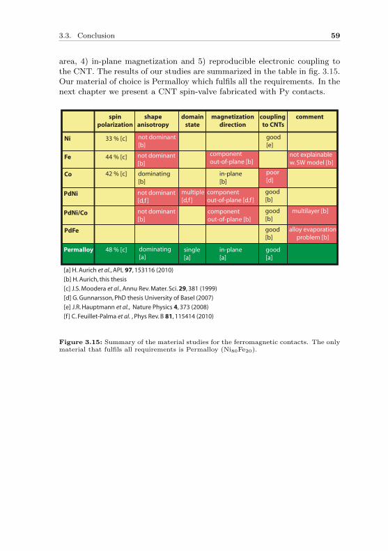
3.3. Conclusion 59
area, 4) in-plane magnetization and 5) reproducible electronic coupling tothe CNT. The results of our studies are summarized in the table in fig. 3.15.Our material of choice is Permalloy which fulfils all the requirements. In thenext chapter we present a CNT spin-valve fabricated with Py contacts.
PdNi
PdNi/Co
PdFe
Fe
Co
Ni
spinpolarization
33 % [c]
42 % [c]
44 % [c]
[c] J.S. Moodera et al., Annu Rev. Mater. Sci. 29, 381 (1999)
shapeanisotropy
dominating[b]
domainstate
magnetizationdirection
in-plane[b]
coupling to CNTs
good[b]
good[b]
multiple[d,f ]
not dominant[d,f ]
componentout-of-plane [d,f ]
componentout-of-plane [b]
poor[d]
comment
not dominant[b]
multilayer [b]
alloy evaporationproblem [b]
good[b]
good[e]
[b] H. Aurich, this thesis
[d] G. Gunnarsson, PhD thesis University of Basel (2007)
[e] J.R. Hauptmann et al., Nature Physics 4, 373 (2008)
[a] H. Aurich et al., APL 97, 153116 (2010)
[f ] C. Feuillet-Palma et al. , Phys Rev. B 81, 115414 (2010)
not dominant[b]
componentout-of-plane [b]
Permalloy 48 % [c] dominating[a]
single[a]
in-plane[a]
good[a]
not dominant[b]
not explainable w. SW model [b]
Figure 3.15: Summary of the material studies for the ferromagnetic contacts. The onlymaterial that fulfils all requirements is Permalloy (Ni80Fe20).

60 Ferromagnetic Materials for Carbon Nanotube Spintronic Devices

Chapter 4Permalloy-based CNT Device
In this chapter we present measurements on a CNT contacted with two ferro-magnetic Py contacts and two Pd contacts. We first discuss the formation ofquantum dots in the segments of the CNT between the different contacts andshow that the inderdot coupling is relatively small. Then we present mea-surements on the spin-valve, defined by the two Py strips and the nanotubesegment in between. We can directly relate the spin-valve characteristics tothe magnetization reversal of our Py contacts found in AMR measurementsof the single strips1. The TMR signal can be tuned with the backgate. Inthe last part of this chapter, we discuss magnetoresistance measurements ina non-local geometry and magnetoresistance effects that could influence ormimic spin-valve behavior.
4.1 Formation of quantum dots
Fig. 4.1 shows an SEM image of a CNT contacted in the center by two Pycontacts (labelled 2 and 3) of width 400 nm and 140 nm, with an edge toedge distance of 370 nm. At the top and bottom two Pd contacts (4 and1) are placed as reference. The Py strips are contacted in a four-terminalgeometry for AMR characterization. The CNT diameter was found by AFMas 1.2 ± 0.3 nm, averaged along a segment of 100 nm. This is a typicaldiameter for an individual single wall CNT [12]. The resistances at roomtemperature between the contacts 1−2, 2−3 and 3−4 are 38, 26 and 20 kΩ,
1Parts of this work have been published in [108].
61

62 Permalloy-based CNT Device
1
2
3
QD1
QD2
QD3
~~
4
V
Py
Pd 1µm
CNT
400 nm
I2
I3
Figure 4.1: False-color SEM image of a CNT contacted by two Py electrodes and 2 Pdreference electrodes. The Py electrodes have a width of 400 nm and 140 nm, respectivelyand are contacted in a four-terminal geometry to measure the individual AMR signals ofthe strips. Their edge to edge distance is 370 nm. The zoom-in shows the CNT contactedby the two Pd electrodes 1 and 4 and the two Py electrodes 2 and 3. Quantum dots(labelled QD1, QD2 and QD3) are forming in between two electrode pairs, when thedevice is cooled to cryogenic temperatures. To measure the coupling of the Py electrodesto the CNT we apply a voltage to a Pd electrode and measure the currents I2 and I3at the two Py electrodes simultaneously.
respectively. No band gap is observed and the CNT behaves like a metal orsmall bandgap semiconductor.
At 230 mK, all segments show Coulomb blockade oscillations as a func-tion of VBG, providing evidence for carrier confinement in these regions.The four contacts divide the CNT into three quantum dots labeled QD1,QD2 and QD3. The differential conductance G = dI/dV for QD2 formingbetween the two Py contacts as a function of the backgate voltage VBG isplotted in fig. 4.2a (G0 = 2e2/h ≈ 7.748 · 10−5 Ω−1). The peak values of theconductance reach 0.85G0, suggesting a strong and quite symmetric cou-pling of the two Py contacts to the CNT. The stability diagram for QD2is shown in the lower part of the figure. The charging energy of the dot is∼ 1.5 meV, an orbital energy is too small to be detected. The lever arm ofthe backgate is η = ∆VSD
∆VBG≈ 0.02. The FWHM ∼ 1 meV. This is much larger
than the broadening by temperature (∼ 0.02 meV for T = 230 mK), whichsuggests that the QD level broadening is dominated by the coupling to theleads (lifetime broadening). Assuming symmetric tunnel coupling results inΓ1 ≈ Γ2 ≈ 0.5 meV.
Fig. 4.2b shows the differential conductance for QD1 forming between thePy contact 2 and the Pd reference electrode 1 as a function of the backgatevoltage. The highest conductance values reach only 0.2G0 suggesting a moreasymmetric coupling of the two contacts. The charging energy and lever arm
extracted from the stability diagram are UC ≈ 1.5 meV and η =β+|β−|β++|β−| ≈

4.1. Formation of quantum dots 63
Pd
-10 -5 0 5 100.0
0.2
0.4
0.6
0.8
1.0
VBG
(V)
G/G
0
-10 -5 0 5 100.00
0.05
0.10
0.15
0.20
VBG
(V)
G/G
0
a) b)QD2 QD1
1.5
-1.5
0
V SD (m
V)
-2.875 -2.625 -2.375
VBG
(V)
∆VSD
∆VBG
0.38 0.42 0.46
2
-2
0
VBG
(V)
V SD (m
V)
0.5
0.3
0.4
G/G0
0.01
0.04
0.07
0.1G/G
0
β+ β-
Figure 4.2: a) Conductance of the QD2 forming between the two Py contacs at lowtemperature (T = 230 mK) as a function of the backgate voltage. The peak values of0.85 G0 suggest a strong symmetric coupling of the contacts. The stability diagram ofQD2 is shown below. b) Coulomb blockade and stability diagram for QD1 (Py-CNT-Pd)at 230 mK.
0.03. For both diagrams the Coulomb diamonds are relatively symmetricsuggesting a quite symmetric capacitive coupling to the leads.
We characterize the coupling of a single Py contact by applying a volt-age to contact 1 and measuring simultaneously the two resulting currentsin the Py terminals 2 and 3 (see schematic in fig. 4.1). Conductance curvesfor a small backgate voltage range of the two dots at low temperature areplotted in the upper part of fig. 4.3a. The green line shows the conduc-tance of QD2 whereas the blue line represents the conductance of QD1 fivetimes magnified. The differential conductance between contacts 1 and 3,essentially given by G31 = I3/V , is shown in black in the lower part ofthe figure and exhibits peak maxima of ∼ 0.004G0, about 30 times smallerthan G21 = I2/V , indicating that most of the current flows into contact2. The transmission T31 = G31/G0 is reproduced very well by the prod-
uct of the transmissions TQD1 =GQD1
G0and TQD2 =
GQD2
G0obtained from
the two-terminal conductances of QD1 and QD2, respectively, and a factorf ≈ 0.075: T31 ≈ fTQD1TQD2. This function is plotted in red in the lowerpart of the figure.

64 Permalloy-based CNT Device
These characteristics are not expected on the first sight. Two quantumdots in series are forming in the device between the contacts 1-2 and 2-3 atlow temperatures as indicated in the schematic in fig. 4.3b. In a classicalpicture for diffusive transport one can consider the dots as two conductorswith conductances GQD1 and GQD2 leading to a total conductance of the
deviceGQD1GQD2
GQD1+GQD2. This already describes the basic shape of the measured
conductance, but shows an overestimation of several features and a generallytoo large total conductance. A similar behavior is also obtained by assuming
QD1 QD2
~~V
I2
I3
a) b)
1
2 3
TQD1
TQD2
R
Ttrans
Tout
c) 1 3
2
1.6 1.7 1.8 1.9 2.0
0
2
4
0.0
0.2
0.4
0.6
G/G
0G
/G0 (%
0)
VBG
(V)
5 x TQD1
TQD2
I3
/ V
f x TQD1
x TQD2
Figure 4.3: a) Upper graph: Coulomb blockade oscillations in the differential conduc-tance as a function of VBG for QD2 (with two Py contacts) plotted in green and QD1plotted in blue (5x magnified) at T = 230 mK. The bottom part shows the conductancebetween contacts 1 and 3 when contact 2 is grounded (black curve). The measuredsignal can be fitted by multiplying the individual transmissions TQD1(2) = GQD1(2)/G0
of the two dots and a factor f ≈ 0.075: T = fTQD1TQD2 (red curve). b) Measurementscheme for the transparency of a contact. A voltage is applied at the Pd contact (gray).Simultaneously, the currents I2 and I3 are measured. Two QDs are forming betweenthe contacts 1-2 and 2-3 respectively. c) The transmission through the individual QDsare TQD1 and TQD2. The red dotted circle discribes the complex situation in the con-tact 2 for electrons comming from QD1. The same situation can be assumed for QD2.Electrons are taken out of the circuit with a transmission rate Tout or reflected in thedot with a reflectivity R. A part of the current is transmitted with transmission Ttrans
to QD2.

4.1. Formation of quantum dots 65
two coherent conductors in series with known transmissions TQD1 and TQD2
[134]: the transmission of two coherent conductors can be expressed by
T =TQD1TQD2
1−2√RQD1RQD2·cos(θ)+RQD1RQD2
with RQD1(2) = 1− TQD1(2) and θ the
phase shift acquired between the reflection processes.
We find that both models are not applicable to describe the observed con-ductance. They both base upon the assumption of two conductors in serieswith known transmissions, measured in individual experiments. However,the situation cannot be described by a simple combination of the two indi-vidual systems. A possible explanation of the measured conductance can begiven by considering the situation depicted in fig. 4.3c. The transmissionsTQD1 and TQD2 of the individual dots are measured between the contacts1-2 and 2-3, respectively. However, when the total transmission T31 between1 and 3 is measured, one finds not only a combination of the two individualmeasurements, there is also a current path in the CNT below the contact2 that has to be included. The schematic in the dotted circle describes thecomplex processes assumed to take place in contact 2 for electrons arrivingfrom dot 1. Comparable processes are assumed for the electrons of dot 2.The current can be reflected with a probability R. This leads to the forma-tion of the QD states. A part of the current is taken out of the system withtransmission Tout. Ttrans describes a small direct transmission of the currentfrom dot 1 to dot 2 under the contact.
When the transmission between the two quantum dots is small, the totalsystem can be described by a Hamiltonian Htot = HQD1 +HQD2 +Ht withHQD1(QD2) describing the individual dots in equilibrium (including R andTout) and Ht is a hopping term evoked by the weak coupling. Assuming aneffective density of states proportional to the measured transmission N1 =ν1TQD1 and N2 = ν2TQD2 (with ν1(2) proportionality factors), describing theprobability to find electrons with a certain energy on the dots, it is possibleto construct the transmission between the dots by Fermi’s golden rule [135]
TQD1→QD2 =2π
~|〈QD1 |Ht|QD2〉|2 N1N2 =
2π
~TtransN1N2 (4.1)
with |QD1〉 and |QD2〉 the initial and final eigenstates of HQD1 +HQD2 and〈QD1 |Ht|QD2〉 the hopping matrix element. Expressing the effective DOSin terms of the transmissions as assumed above leads to
TQD1→QD2 =2π
~Ttrans
1
ν1ν2︸ ︷︷ ︸f
TQD1TQD2 ≡ fTQD1TQD2 (4.2)
with f defined as the proportionality factor observed above. The modelshows that the observed transmission can be explained by two strongly de-

66 Permalloy-based CNT Device
coupled coherent subsystems with a small transmission.
Applying the bias on contact 4 (not shown) through the more transparentQD3 and measuring the conductances G43 and G42 yields ∼ 8 times smallercurrent in the second Py contact than in the first along the current direction.A possible explanation is a weaker coupling of the narrower Py contact tothe CNT if one assumes a distributed contact with current transported inthe CNT under the contact [136].
4.2 CNT spin-valve
The two Permalloy contacts 2 and 3 and the carbon nanotube segment forma lateral CNT spin-valve. We observed sharp TMR switchings that candirectly be related to the AMR of the individual contacts [108]. The sizeand sign of the measured TMR can be tuned with the backgate voltage. Allmagnetoresistance measurements presented here were done at 230 mK.
4.2.1 Relation of the TMR to contact switching effects
An example of a TMR measurement is plotted in fig. 4.4. The differentialconductance of QD2 between the Py contacts is shown as a function of theexternal magnetic field applied along the Py strips. The backgate voltagewas fixed at 0.656 V, corresponding to a Coulomb oscillation maximum. We
-200 -100 0 100 200
0,60
0,63
0,66
µ0H (mT)
G/G
0
∆R/R
0∆R
/R0
(pp
m)
(pp
m)
100
25
AMR 2
AMR 3
GP
GAP
TMR =G
P - G
AP
GAP
Figure 4.4: TMR signal between two Py contacts on a Coulomb oscillation maximum asa function of the external magnetic field applied parallel to the contacts. The relativemagnetization directions of the contacts are indicated by arrows. The conductanceshows sharp changes at the magnetic fields of ± 26 mT and ± 58 mT, respectively. Thesevalues correspond very well to the fields of magnetization reversal for the two Permalloycontacts. The top and bottom curves in the graph are the AMR signals of the individualPy contacts 2 (AMR 2) and 3 (AMR3).

4.2. CNT spin-valve 67
find sharp switchings of µ0∆H < 1 mT (corresponding to the measurementstep size) with an amplitude of ∼ 4.5 % at the magnetic fields ± 26 mT and± 58 mT. The switching fields determined from the TMR measurements cor-respond very well to the fields of magnetization reversal in the Py contactsfound in the AMR measurement of the individual contacts, plotted aboveand below the conductance curves in fig. 4.4. The relative magnetizationorientations of the electrodes are indicated in the figure. In addition to thesharp switching a gradual conductance change with the magnetic field is ob-served (∼ 0.01G0/200 mT), tentatively attributed to small domain rotationsdue to the magnetic field.
If the spin polarization of the Py contacts is calculated using Julliere’smodel with this TMR value assuming equally polarized contacts, we findP ∼ 15 %, considerably smaller than expected from the bulk polarization.In the next section we show that Julliere’s model is too simple to describeour device and that the nanostructure is crucial to the spin-valve.
4.2.2 Tunability of the TMR signal
The conductance traces presented above are measured at a fixed backgatevoltage corresponding to a Coulomb blockade maximum. We find a strongdependence of the TMR on VBG. Fig. 4.5a shows the conductance over VBG
of QD2 in a small backgate voltage range. The position where the TMRin fig. 4.4 has been measured is indicated by a blue square. Another TMRmeasurement is done on a Coulomb blockade peak at a backgate voltageof 0.745 V and the measured conductance over the magnetic field can beseen in fig. 4.5b. The position is labelled by a green square in the conduc-tance graph. The shape of the measured conductance traces is similar tothe signal measured on the other peak but the amplitude of the TMR issmaller (TMR ∼ 1.5 %). The observed background is similar to the back-ground observed in fig. 4.4 but with a smaller change in conductance withthe magnetic field (∼ 0.005G0/200 mT). A TMR measurement between twoCoulomb blockade peaks in a valley (yellow square, VBG = 0.692 V) showsan increase of conductance when the contacts switch from the parallel tothe antiparallel state (fig. 4.5c). This leads to a negative TMR with anamplitude of ∼ −2.7 %. The background of this measurement is quite un-stable. It is not possible to determine its exact shape due to sample in-stabilities. However, the switching features are still visible very well. Theblack line in fig. 4.5d is the conductance in the parallel configuration. Dueto problems with the device instability it was not possible to measure thecorresponding conductance trace for the antiparallel configuration. (Deviceinstabilities are discussed in chapter 2 and appendix B.) We find an oscil-lating behavior of the TMR between +5.5 % and −2.7 % with the backgate

68 Permalloy-based CNT Device
-0.2 -0.1 0 0.1 0.2
0.28
0.29
0.30
0.31
-0.2 -0.1 0 0.1 0.20.705
0.710
0.715
0.720
0.725
0.6 0.7 0.8 0.90.0
0.2
0.4
0.6
0.8
-6-4-20246
0.5 0.6 0.7 0.8 0.9 1.00.0
0.2
0.4
0.6
0.8
G/G
0
VBG
(V)
G/G
0
µ0H (T)
µ0H (T)
G/G
0 G/G
0
VBG
(V)
TMR
(%)
a) b)
c) d)
G
TMRguide
Figure 4.5: a) Coulomb oscillations of the conductance G of QD2 with VBG. Theblue square indicates the position where the signal in fig. 4.4 has been measured. Mea-surements on the green and yellow marked positions can be seen in b) and c). b) Theconductance depending on the magnetic field on the Coulomb blockade maximum has asimilar shape to the signal in fig. 4.4. c) In a Coulomb blockade valley the conductanceincreases in the antiparallel configuration and the TMR signal changes sign. d) The sizeof the TMR is plotted for different VBG in one graph together with the conductance ofthe device (black line). The grey line is a guide to the eye.
voltage. We obtain positive values for the TMR when the QD is tuned to aCoulomb blockade maximum and negative values for measurements betweentwo Coulomb peaks. The gray line is a guide to the eye interpolating theoscillatory behavior of the TMR.
Oscillations of the TMR with VBG in multi wall and single wall CNTdevices have been observed for the first time by Sahoo et al. [19]. However,the results presented in this thesis are in contradiction to their observations,where TMR < 0 on Coulomb blockade peaks and TMR > 0 in the valleysin-between are documented.
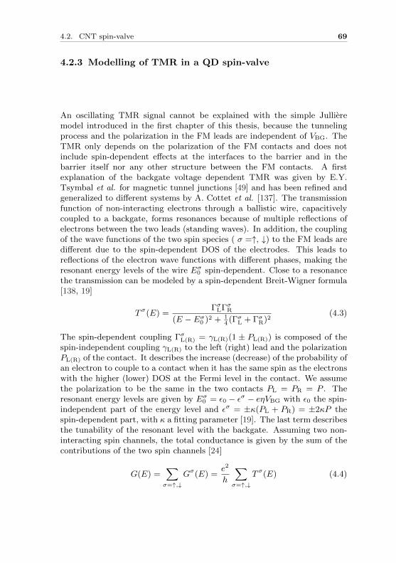
4.2. CNT spin-valve 69
4.2.3 Modelling of TMR in a QD spin-valve
An oscillating TMR signal cannot be explained with the simple Jullieremodel introduced in the first chapter of this thesis, because the tunnelingprocess and the polarization in the FM leads are independent of VBG. TheTMR only depends on the polarization of the FM contacts and does notinclude spin-dependent effects at the interfaces to the barrier and in thebarrier itself nor any other structure between the FM contacts. A firstexplanation of the backgate voltage dependent TMR was given by E.Y.Tsymbal et al. for magnetic tunnel junctions [49] and has been refined andgeneralized to different systems by A. Cottet et al. [137]. The transmissionfunction of non-interacting electrons through a ballistic wire, capacitivelycoupled to a backgate, forms resonances because of multiple reflections ofelectrons between the two leads (standing waves). In addition, the couplingof the wave functions of the two spin species ( σ =↑, ↓) to the FM leads aredifferent due to the spin-dependent DOS of the electrodes. This leads toreflections of the electron wave functions with different phases, making theresonant energy levels of the wire Eσ0 spin-dependent. Close to a resonancethe transmission can be modeled by a spin-dependent Breit-Wigner formula[138, 19]
Tσ(E) =ΓσLΓσR
(E − Eσ0 )2 + 14(ΓσL + ΓσR)2
(4.3)
The spin-dependent coupling ΓσL(R) = γL(R)(1 ± PL(R)) is composed of thespin-independent coupling γL(R) to the left (right) lead and the polarizationPL(R) of the contact. It describes the increase (decrease) of the probability ofan electron to couple to a contact when it has the same spin as the electronswith the higher (lower) DOS at the Fermi level in the contact. We assumethe polarization to be the same in the two contacts PL = PR = P . Theresonant energy levels are given by Eσ0 = ε0 − εσ − eηVBG with ε0 the spin-independent part of the energy level and εσ = ±κ(PL + PR) = ±2κP thespin-dependent part, with κ a fitting parameter [19]. The last term describesthe tunability of the resonant level with the backgate. Assuming two non-interacting spin channels, the total conductance is given by the sum of thecontributions of the two spin channels [24]
G(E) =∑σ=↑,↓
Gσ(E) =e2
h
∑σ=↑,↓
Tσ(E) (4.4)

70 Permalloy-based CNT Device
and when we plug in equation 4.3 the conductance for parallel and antipar-allel configuration of the electrode magnetizations can be expressed as
GP =e2
h
[Γ↑LΓ↑R
(E − E↑0 )2 + 14(Γ↑L + Γ↑R)2
+Γ↓LΓ↓R
(E − E↓0 )2 + 14(Γ↓L + Γ↓R)2
](4.5)
GAP =e2
h
[Γ↑LΓ↓R
(E − E↑0 )2 + 14(Γ↑L + Γ↓R)2
+Γ↓LΓ↑R
(E − E↓0 )2 + 14(Γ↓L + Γ↑R)2
].
(4.6)
The first (second) term in the case of parallel conductance describes thetransmission for electrons coming from a state with a high (low) DOS at theFermi level and entering a state with a high (low) DOS at the Fermi levelin the second electrode. The resonant energies are different for the two spinchannels. In the case of antiparallel orientation of the contact magnetizationthe first term describes electrons with the spin-dependent resonant energyE↑0 coming from a state with a high DOS at the Fermi level entering a statewith a low DOS in the second electrode and vice versa for the second term.
To study the behavior of the conductances in the parallel and antiparallelelectrode configuration, different cases can be considered:
Spin-independent resonant energy level
In the first case we assume the resonant energy level to be spin-independent(E↑0 = E↓0 = E0). The conductances far away from the resonant levelE − E0 >> (ΓσL + ΓσR) can be written as
GP ∼(
Γ↑LΓ↑R + Γ↓LΓ↓R
)∝ 1 + P 2 (4.7)
and
GAP ∼(
Γ↑LΓ↓R + Γ↓LΓ↑R
)∝ 1− P 2 (4.8)
for the parallel and the antiparallel configuration, respectively. The TMR =GP−GAPGAP
= 2P2
1−P2 obtained in this case is always positive independent of thecoupling asymmetry.
In the resonant case E − E0 ≈ 0, one has to distinguish between sym-metric and asymmetric coupling of the contacts. Sahoo et al. [19] assumedvery asymmetric coupling (γR >> γL), resulting in a negative TMR =
− 2P2
1+P2 < 0. This behavior is plotted in red in the upper graph of fig. 4.6a for

4.2. CNT spin-valve 71
γL = 0.1 meV and γR = 0.9 meV (the other parameters are ε0 = 0, κ = 0)2.The conductances in the parallel and antiparallel configuration are plottedin black and gray, respectively. The assumption of an asymmetric couplingis proper to decribe the observation by Sahoo et al.. More symmetric cou-pling can result in a positive TMR in the resonant case as shown in theupper graph in fig. 4.6b. The model uses γL = γR = 0.5 meV as foundexperimentally.
The TMR on the Coulomb blockade maximum is plotted for increasingasymmetry γR/γL with γL = 0.5 meV in fig. 4.6c (red line). It turns negativefor an asymmetry of ∼ 4. Therefore, a coupling with a small enough asym-metry could indeed explain our observation of TMR > 0 in the resonantcase. However, the TMR measured off-resonance at the position VBG = 0.2 V(plotted in green) is always positive in this model not in agreement with ourexperiment. Arrow 1 indicates the region where a signal as in ref. [19] canbe observed but a measurement as indicated by arrow 2 is not observed forour device.
The two color scale plots in fig. 4.6c on the right show again the TMRfor different combinations of coupling constants off and on a resonance. TheTMR in the off-resonance case (at VBG = 0.2 V) is positive also for highasymmetries. For even higher asymmetries than plotted in the graph it isnot reasonable still to talk about off-resonance because of the increased peakwidth. For the on-resonance situation regions with positive and negativeTMR can be seen. The white dotted lines correspond to the situationsplotted in the left graph.
Spin-dependent resonant energy level
A strong splitting of the resonant energy levels ∆E0 = E↑0 − E↓0 can lead
to an oscillating TMR with VBG. One can imagine the level splitting ∆E0
to be induced by spin-dependent interfacial phase shifts (SDIPS) [137]. Thespin-dependent phase shifts can be due to a different scattering of electronswith spin orientation parallel and antiparallel to the contact magnetizationat the interface between the wire and the FM contact. In the asymmetriccase the level splitting can lead to the behavior plotted in the lower graphof fig. 4.6a (κ = 0.5 meV). The conductance peaks for the parallel and theantiparallel alignment of the electrodes are deformed and slightly shiftedwith respect to each other. As a result, the TMR oscillates between positiveand negative values on and off the resonances. In the case of symmetriccoupling a similar behavior is observed as can be seen in the lower graph offig. 4.6b. Oscillations in the conductance close to a resonance are possible.
2We use here the experimental result that the sum of the coupling constants is ∼ 1 meVand assume an asymmetry of 1:9.

72 Permalloy-based CNT Device
1
0.5
0
20
10
0
0.4
0.2
0.0
30
10
-10
0.0
0.3
0
50
-50
-0.2 -0.1 0.0 0.1 0.2
1
0
20
10
0
-10
TMR
(%)
1 5 73 9γ
R/γ
L
γL= 0.5 meV
20
-20
0
-0.2 -0.1 0.0 0.1 0.2
VBG
(V)VBG
(V)
G/G
0
G/G
0TM
R (%
)
TMR
(%)
γL= γ
R=0.5 meVγ
L= 0.1 meV; γ
R=0.9 meV
κ=0.5 meV κ=0.5 meV
>0<0
>0>0
>0
<0 <0<0
>0
b)a)
c)
1
2
GP
GAP
GP
GAP
GP
GAP
GP
GAP
5
23
4
2 3 4 5
6 10 14 18
γR (meV)
γ L (meV
)
TMR (%)
5
23
4
γ L (meV
)
2 3 4 5γ
R (meV)
-15-10 -5 0 5TMR (%)
10
off resonance on resonance
0.50.5
0.50.5
off res
on res
Figure 4.6: Calculated conductances GP (black line), GAP (gray line) and TMR (redline) for: a) the asymmetric case γL = 0.1 meV and γR = 0.9 meV. The upper graphshows the result for ε0 = 0 and κ = 0. A negative TMR on the peak is found. Inthe lower graph ε0 = 0 and κ = 0.5 meV. The TMR can be positive or negative in theresonant case. b) the symmetric case γL = γR = 0.5 meV. For ε0 = 0 and κ = 0, theTMR is always positive in the resonant case (upper graph). It is also positive on theresonance for κ = 0.5 meV, but can be negative close to it. c) Plot of the TMR on(red) and off (green) a Coulomb peak as a function of the coupling asymmetry. Ref.[19] assumes asymmetric coupling measuring a TMR signal as proposed by arrow 1.We assume more symmetric coupling, however the predicted result indicated by arrow2 is not observed. The graphs on the right show a colorscale plot for the TMR independence of the coupling asymmetry. In the off-resonance case the TMR is alwayspositive whereas in the on-resonance case it changes sign. The white dotted line marksthe situation plotted on the left.
With the help of this simple model it is possible to understand the originof magnetoresistance oscillations with the backgate voltage and the obser-

4.2. CNT spin-valve 73
vation of positive or negative TMR on Coulomb blockade peaks, but it isnot possible to reproduce the guide to the eye in fig. 4.5d) in our experi-ment. Additionally, it should be noted that the number of data point in ourgraph is very low, probably preventing the observation of substructures inthe magnetoresistance signal that could be modelled with the assumptionsmade above.
In the model described above electron-electron interactions were neglected.In the Coulomb blockade regime they can have a considerable influence asshown by Cottet et al. [137, 139], who studied a quantum dot coupled totwo FM leads in an Anderson model and calculated the conductance usingan equation of motion technique. In their model they assumed a two-orbitalQD with K − K′ orbital degeneracy. SDIPS were taken into account as
incr
easi
ng
SD
IPS
Figure 4.7: Figure taken from [139]. Calculated conductances GP (red line) and GAP
(black dotted line) of a two-orbital quantum dot. The tunnel rates are ΓL = 0.0043U andΓR = 0.0725U with U = 30kT . The contact polarization is 0.4 for both contacts, α ishere the lever arm of the backgate. The energy splittings of the resonances are increasingfrom top (∆E = 0.00U) to bottom (∆E = 0.3U) as indicated in the figure. The pinklines represent the tunnel magnetoresistance corresponding to the conductances in theleft figures.

74 Permalloy-based CNT Device
parameters and are manifested in an effective spin-splitting of the dot en-ergy levels, describable by an effective Zeeman splitting. Fig. 4.7 shows aplot taken from [139] for a symmetrically coupled CNT quantum dot witha doubly degenerate level. In the graphs on the left side the conductance inthe parallel (red lines) and antiparallel (black dotted lines) configuration areplotted. The first two peaks correspond to the single occupation of K andK′, the other two to double occupation. In fig. 4.7a no SDIPS are assumed.The TMR signal (fig. 4.7b, plotted in pink) is positive everywhere. TheSDIPS parameter is added in fig. 4.7c and strongly increased in fig. 4.7e.Increasing the SDIPS leads to a strong shift of the conductance in the par-allel and antiparallel case manifesting itself in strong TMR oscillations. TheTMR signals plotted in fig. 4.7d and fig. 4.7f bear significant similarities toour experiments.
However, the origin of such SDIPS is not entirely clear. In addition toboundary scattering effects it is also possible that ferromagnetic impuritiesat the interfaces or ferromagnetic exchange coupling of the dot electrons tothe leads [140] can influence the resonance conditions of the different spinchannels.
4.3 Non-local geometry - preliminary results
The TMR signals discussed so far have been measured in a local or 2-terminalspin-valve geometry with two FM electrodes used to inject a spin polarizedcurrent into the CNT and to measure simultaneously the voltage drop onthe same electrodes. However, magnetoresistance effects due to the FMcontacts like anisotropic magnetoresistance effects [35], magneto Coulombeffects [141] or stray field effects in the CNT can distort or mimic the spintransport signal. Non-local measurement techniques offer the possibility toseparate the spin current from the charge current and can help to distinguishthose additional MR effects from spin accumulation.
In 1985 Johnson and Silsbee proposed a measurement set-up by which thecharge current in a metal structure in the diffusive limit can be separatedfrom the spin signal [30]. The basic measurement scheme is illustrated infig. 4.8. In the non-local or 4-terminal geometry a spin polarized currentis injected into the metal by an FM electrode (3). Contact 4 is grounded,whereas the contacts 2 and 1 are floating. Therefore, a charge current onlyflows between 3 and 4. The injection of spin-polarized charges leads to a spinaccumulation below 3. The different electrochemical potential µ↑ and µ↓ forthe majority spins (↑) and minority spins (↓) are shown in the lower part ofthe figure. The spin accumulation, i.e. the difference in the electrochemicalpotentials for up- and down-spins, diffuses to both sides of the contact,
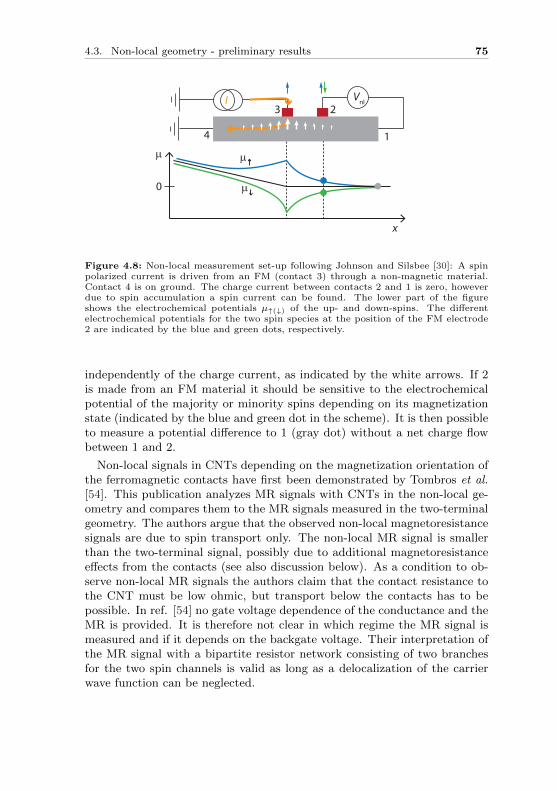
4.3. Non-local geometry - preliminary results 75
x
1
23
4
I Vnl
µ
0
µ
µ
Figure 4.8: Non-local measurement set-up following Johnson and Silsbee [30]: A spinpolarized current is driven from an FM (contact 3) through a non-magnetic material.Contact 4 is on ground. The charge current between contacts 2 and 1 is zero, howeverdue to spin accumulation a spin current can be found. The lower part of the figureshows the electrochemical potentials µ↑(↓) of the up- and down-spins. The differentelectrochemical potentials for the two spin species at the position of the FM electrode2 are indicated by the blue and green dots, respectively.
independently of the charge current, as indicated by the white arrows. If 2is made from an FM material it should be sensitive to the electrochemicalpotential of the majority or minority spins depending on its magnetizationstate (indicated by the blue and green dot in the scheme). It is then possibleto measure a potential difference to 1 (gray dot) without a net charge flowbetween 1 and 2.
Non-local signals in CNTs depending on the magnetization orientation ofthe ferromagnetic contacts have first been demonstrated by Tombros et al.[54]. This publication analyzes MR signals with CNTs in the non-local ge-ometry and compares them to the MR signals measured in the two-terminalgeometry. The authors argue that the observed non-local magnetoresistancesignals are due to spin transport only. The non-local MR signal is smallerthan the two-terminal signal, possibly due to additional magnetoresistanceeffects from the contacts (see also discussion below). As a condition to ob-serve non-local MR signals the authors claim that the contact resistance tothe CNT must be low ohmic, but transport below the contacts has to bepossible. In ref. [54] no gate voltage dependence of the conductance and theMR is provided. It is therefore not clear in which regime the MR signal ismeasured and if it depends on the backgate voltage. Their interpretation ofthe MR signal with a bipartite resistor network consisting of two branchesfor the two spin channels is valid as long as a delocalization of the carrierwave function can be neglected.

76 Permalloy-based CNT Device
A spin-signal in the non-local voltage of a CNT in the coherent non-interacting regime contacted with FM and non-magnetic metal electrodeshas been investigated by Feuillet-Palma et al. [104]. A non-local MR tun-able by a gate voltage due to quantum interference was observed, as pre-dicted theoretically [142]. The non-interacting scattering model assumesconservation of spin and orbital degree of freedom during transport. Thedependence of the signal on the magnetization orientations of the contacts isinduced by spin-dependent resonant effects due to SDIPS. In transport ex-periments in the non-interacting coherent regime, the wave functions extendover the whole length of the CNT, therefore charge transport is not sepa-rated from the spin transport and the MR signal is non-local with respectto the position of the FM and non-magnetic electrodes [104].
A schematic of our ’non-local set-up’ with a CNT is shown in fig. 4.9a. Thecurrent is injected at the narrow Py contact 3 and contact 4 is grounded. Thevoltage is probed between the contacts 1 and 2 (input impedance 1 GΩ).A non-local measurement at VBG = 0 V obtained by injecting a currentof I ≈ 1 nA between 3 and 4 is shown in fig. 4.9b. We measure a non-local voltage Vnl between 1 and 2 and define the non-local conductance asGnl = I/Vnl ≈ 230µS. At the magnetic fields where the FM contacts reversetheir magnetization, known from AMR measurements, steplike changes inthe conduction are observed. The regions with an antiparallel alignment ofthe contact magnetizations are shaded in gray in the figure. This non-localMR has a size of MRnl = (Gnl,P−Gnl,AP)/Gnl,AP ≈ −4.7 %. An increase in
Vnl
23
a) b)
I
14
-60 -40 -20 0 20 40 60200
220
240
260
I / V
nl (µ
S)
µ0H (mT)
Figure 4.9: a) Schematic of a non-local measurement geometry. A spin polarizedcurrent is driven from the FM contact 3 through the nanotube and extracted at contact4. The charge current between contacts 2 and 1 is zero, however due to spin accumulationa spin current can be found. b) Non-local MR signal of the device. Switching featuresat the expected positions can be seen. The shaded areas mark the regions where thecontacts are aligned antiparallel.

4.4. Discussion of other magnetoresistance effects 77
the conductance in the antiparallel situation is consistent with the injectionof majority spin electrons into the CNT from contact 3 in a diffusive picture.The majority spins in contact 2, aligned antiparallel to contact 3, have anopposite orientation to the accumulated electron spins and this causes areduction in Vnl and thereby an increase in Gnl = I/Vnl as also observed inexperiments with diffusive Si nanowires [52]. The noise level is ∼ 8µS, thesame order of magnitude as the observed switching features (signal-to-noiseratio ∼ 1.3). The observed background is rather flat but suffers from a driftand several small jumps due to device instabilities.
The measurement shows a resistance in the non-local geometry with switch-ing features at the magnetic fields where the contacts change their magne-tization. However, it is not straightforward to draw a conclusion from themagnetoresistance measurements in the non-local geometry in the two pub-lications presented above for our device. We observe three quantum dotsthat are weakly but coherently coupled to each other. The regime where theexperiments in the first publication has been performed is not known and theinterpretation corresponds to a diffusive picture of spin accumulation. Thesecond publication studies transport in a non-interacting coherent regimeand cannot be compared to our measurements. Unfortunately, it was notpossible to measure the non-local MR as a function of the backgate voltagedue to electrical instabilities of the device. This would have allowed a directcomparison of local and non-local signals in the Coulomb blockade regime.
4.4 Discussion of other magnetoresistance effects
As shown above, magnetoresistance effects can be induced in CNTs withFM contacts due to spin-polarized transport. However, miscellaneous MReffects in the contacts can also be responsible for resistance change in a two-terminal transport experiment. We now provide a general discussion of sucheffects in relation to our experiment.
Anisotropic magnetoresistance effects
The electrical resistance of an FM electrode is not constant when an externalmagnetic field is applied. The AMR leads to gradually or step-like changesin resistance that can also be important in spin-transport measurements.This has e.g. been shown in all-metal spin-valve devices where the deviceresistance is dominated by the electrode resistances [143]. However, thissmall effect can be neglected for spin-valves dominated by a high tunnelresistance.
For very thin FM films (< a few nanometers) it is shown that the mag-netoresistance is dominated by electron tunneling between different islands

78 Permalloy-based CNT Device
with different magnetization. At a certain thickness, when the islands coa-lesce, the resistance gets dominated by the AMR effect [144]. A comparableeffect could also be imagined for multi-domain contacts consisting of grainswith different magnetizations. It can be possible to have a TMR-like switch-ing in the AMR signal that might also show in the spin-valve signal. Thecurrent in the FM electrode is then described by tunneling from one FM is-land in the material to the next. However, it is not clear how this will changethe tunneling MR signal between two electrodes because it will depend onthe location of the grains.
Another effect that can be considered is the tunneling AMR or TAMReffect. It can cause the switching characteristics of the injection contact tomodulate the TMR. TAMR originates from spin-orbit coupling in an FMelectrode with crystalline anisotropy and is most important for FM materialswith a large SOI like FM semiconductors [145] but is also observed in FMmetals [146]. Changes of the magnetization vector of the contact can betranslated into a change in DOS by the spin-orbit coupling. This leads to achange in TMR.
The previous two arguments could in principle also lead to a spin-valvelike signal in the device if only one FM contact is used, due to multipleswitchings in one contact. However, it is very unlikely that one of thoseeffects is important in our experiments because they would also show in AMRmeasurements. The AMR is well understood for our devices. We measurethe AMR in our contacts and can explain their behavior in an externalmagnetic field by a Stoner-Wohlfarth like model for a single magnetic domainparticle. The AMR signals show no additional features and coincide exactlywith the observed spin-valve signal.
Magneto Coulomb effect
The magneto Coulomb effect (MCE) demonstrated by Ono et al. [141] inmetallic structures could in principle also be relevant in CNT spin transportdevices with FM contacts, as predicted by van der Molen et al. [147]. It hasbeen demonstrated in InP nanowire devices that a magnetoresistance signal,controlled in sign and magnitude by an electric field, can be due to the MCEeven if the device is contacted by only one FM and one non-magnetic contact[148].
The origin of MCE can be explained as follows: An external magneticfield leads to a Zeeman shift of the spin-up and spin-down bands in an FMcontact. An FM material has a different DOS at the Fermi level for the twospin species. Therefore, the chemical potential of the FM is adjusted dueto the repopulation of the empty states. When the FM is in contact with anon-magnetic lead, the electrochemical potential at the interface has to stay
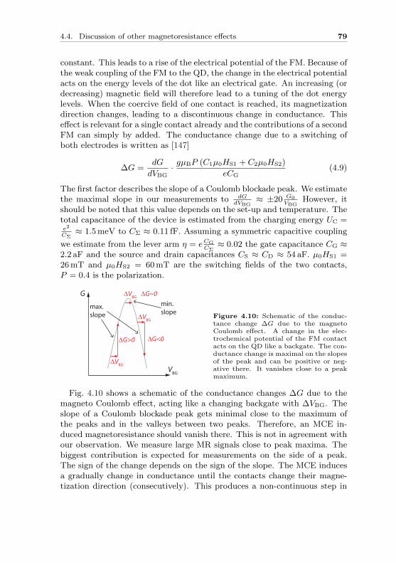
4.4. Discussion of other magnetoresistance effects 79
constant. This leads to a rise of the electrical potential of the FM. Because ofthe weak coupling of the FM to the QD, the change in the electrical potentialacts on the energy levels of the dot like an electrical gate. An increasing (ordecreasing) magnetic field will therefore lead to a tuning of the dot energylevels. When the coercive field of one contact is reached, its magnetizationdirection changes, leading to a discontinuous change in conductance. Thiseffect is relevant for a single contact already and the contributions of a secondFM can simply by added. The conductance change due to a switching ofboth electrodes is written as [147]
∆G =dG
dVBG· gµBP (C1µ0HS1 + C2µ0HS2)
eCG(4.9)
The first factor describes the slope of a Coulomb blockade peak. We estimatethe maximal slope in our measurements to dG
dVBG≈ ±20 G0
VBGHowever, it
should be noted that this value depends on the set-up and temperature. Thetotal capacitance of the device is estimated from the charging energy UC =e2
CΣ≈ 1.5 meV to CΣ ≈ 0.11 fF. Assuming a symmetric capacitive coupling
we estimate from the lever arm η = eCGCΣ≈ 0.02 the gate capacitance CG ≈
2.2 aF and the source and drain capacitances CS ≈ CD ≈ 54 aF. µ0HS1 =26 mT and µ0HS2 = 60 mT are the switching fields of the two contacts,P = 0.4 is the polarization.
G
VBG
∆VBG
∆VBG
∆VBG
∆G>0 ∆G<0
∆G~0
max. slope
min. slope
Figure 4.10: Schematic of the conduc-tance change ∆G due to the magnetoCoulomb effect. A change in the elec-trochemical potential of the FM contactacts on the QD like a backgate. The con-ductance change is maximal on the slopesof the peak and can be positive or neg-ative there. It vanishes close to a peakmaximum.
Fig. 4.10 shows a schematic of the conductance changes ∆G due to themagneto Coulomb effect, acting like a changing backgate with ∆VBG. Theslope of a Coulomb blockade peak gets minimal close to the maximum ofthe peaks and in the valleys between two peaks. Therefore, an MCE in-duced magnetoresistance should vanish there. This is not in agreement withour observation. We measure large MR signals close to peak maxima. Thebiggest contribution is expected for measurements on the side of a peak.The sign of the change depends on the sign of the slope. The MCE inducesa gradually change in conductance until the contacts change their magne-tization direction (consecutively). This produces a non-continuous step in

80 Permalloy-based CNT Device
conductance of ∼ 0.002G0 which is to small to detect in our experiment(noise level ∼ 0.002G0).
The above described situation gives a small contribution to the MR signalin the spin-valve. However, a spin-valve like signal has different characteris-tics and can easily be discriminated3.
Stray field effects
In addition to the applied external magnetic field, a stray field producedby an FM contact can act on the magnetic moments of the electrons in aQD. According to the analytical model provided in [149], the stray field of a300 nm wide rectangular Permalloy contact, magnetized along its long axis,is around 30µT close to the edge of the contact and similar in a distanceof ∼ 200 nm where the QD probably forms. This stray field leads to aZeeman energy of 1/2gµBB ≈ 1.7 · 10−9eV (with g = 2). This energy shiftof the Coulomb blockade peak leads to a change in conductance ∆G =∂G∂VBG
· ∂VBG∂E·∆E. The first factor describes the maximal slope on the side
of a Coulomb peak. We estimate ∂G∂VBG
< 20 G0VBG
for our device, however theslope depends on the set-up and the temperature. The second factor is theinverse lever arm.
For a stray field of 30µT the maximal energy shift is ∼ 1.7 · 10−6 G0 andis therefore difficult to observe. An observable effect would be obtained bymagnetizing the contacts along their width or their height. The calculatedstray field due to a magnetization in one of these directions can be as highas 1 T close to the contact. The Zeeman energy is then calculated to ≈5.8 · 10−5 eV leading to non-negligible conductance changes of ∼ 0.06G0.
4.5 Conclusion
In this chapter we discussed a Permalloy-based CNT device with two Pyand two Pd contacts. We showed that Py contacts couple strongly the theCNT, thereby forming quantum dots at low temperatures. The QDs areweakly coupled and the transmission through two dots can be modelled byfTQD1TQD2 with f a small transmission between the two dots. We founda spin-valve behavior with sharp switching features for the CNT contactedwith two Py electrodes. The switching features of the MR device can directlybe related to the magnetization reversal of the individual contacts. A back-gate tunable magnetoresistance was studied in a two terminal measurement.
3It should be noted that a spin-valve like signal in a device with only one FM and onenon-magnetic contact was also observed in ref. [148]. This can be possible if the FMcontact shows two magnetization switchings. However, this switchings should alsobe visible in AMR measurements and are very unlikely in our device.

4.5. Conclusion 81
The magnetoresistance was found to be modulated by the backgate voltagebetween +4.5 % and −2.7 %. The observed TMR is positive on Coulombblockade peaks and negative off the peak in contrast to literature report andcan probably be explained by spin-dependent resonant states. A MR effectis also observed in a non-local geometry. However, due to instabilities ofthe quantum dots it was not possible to compare non-local with local TMRsignals.

82 Permalloy-based CNT Device

Chapter 5Summary and Outlook
In this thesis different ferromagnetic materials were studied for their suit-ability as contact material for carbon nanotube spintronic devices. Therequirements that have to be met by the FM contacts are 1) a large spinpolarization, 2) the shape anisotropy dominates the crystal anisotropy, 3) asingle magnetic domain covering the contact area, 4) in-plane magnetizationand 5) reproducible electronic coupling to the CNT. We find that Permalloy(Py, Ni80Fe20) fulfils all our requirements [108]. The investigated Py con-tacts show an in-plane magnetization well aligned with the long axis of thestrip. The switching of the magnetization in external magnetic fields canbe modelled by a Stoner-Wohlfarth model for single-domain particles andthe switching fields of the contacts can be reproducibly tuned by the widthof the strips on technically and experimentally useful scales. Py provides astrong coupling and good electrical contact to CNTs comparable to the non-magnetic Pd which is known as the best contact material to contact CNTs[90]. For this purpose, the formation of quantum dots is demonstrated atlow temperatures. A CNT device with two Py electrodes shows spin-valvebehavior with sharp switching features, directly related to the magnetizationreversal of the individual contacts. The magnetoresistance of the spin-valveis electrically tunable in size and sign by an external gate.
A possible experiment in the near future can be a Hanle spin precessionmeasurement in a CNT QD coupled to two Py contacts. It is suggested thatin transport experiments through an individual single-level QD it is possi-ble to measure directly the spin-decoherence time T2 of the individual spins,whereas in optical realizations of Hanle experiments the spin-dephasing timeT ∗2 , averaged over a spin ensemble, is measured [10]. Another experiment
83

84 Summary and Outlook
can make use of the strong coupling of Py to CNTs to study the magne-toresistance of a spin-valve in the Kondo regime or investigate the exchangeinteraction of a CNT state and the leads [150].
The aim in future experiments is to use the Py contacts on CNTs for spinprojection measurements in electron entanglement experiments. Hofstet-ter et al. [73] recently realized a Cooper pair splitter in a semiconductingnanowire. A Cooper pair is injected from a superconducting lead into asemiconducting nanowire and split by Coulomb interactions. The splittingof Cooper pairs was succesfully shown, but to determine the degree of entan-glement between the electrons, an analyzing tool e.g. ferromagnetic contactsare needed. Here comes the advantage of CNTs into play. Due to their smalldiameter it is easier to contact CNTs with FM contacts. The typical diam-eter of a semiconducting nanowire is a few ten nanometers, larger than thethickness of the Py contacts studied in this thesis. When the contact hasto follow the shape of the nanowire this will lead to large stray fields andmulti-domains states in the contact (see e.g. [143]). The spin states ofthe individual electrons are projected to the magnetization direction of thecontacts. Two FM contacts with different switching fields can be used tomeasure the current correlations in the device in the parallel and antiparallelaligned configuration. However, this simple geometry is not sufficient to dis-tinguish between an entangled state and a two-particle product state [151].Spin-projection measurements in different directions are needed to prove theentanglement [152]. A possible realization of this idea is to replace one ofthe FM contacts with a synthetic antiferromagnetic (SAF) [153] disk con-
Py
Py
Ru
a) b)
SAF
1 µm
CNT
Py
Figure 5.1: a) Schematic of a (simple) SAF disk. Two ferromagnetic Py layers areseparated by a non-magnetic Ru layer. The magnetization of the Py layers align an-tiparallel and can be controlled by an external magnetic field. b) False-color SEM imageof a CNT contacted with a Py strip and a Py/Ru multilayer SAF disk. The selectablemagnetization direction of the disk allows spin projection measurements with differentangles between the magnetization direction of the disk and the strip. The SEM imageis kindly provided by Julia Samm.

85
sisting of a Py/Ru multilayer structure as shown schematically in fig. 5.1a.The magnetization direction of the disk can be set by an external magneticfield in any desired direction. For the right choice of the thickness of theRu interlayer the magnetizations of the FM layers will show anti-parallelalignment leading to a minimization of the stray field of the disk1. An SEMimage of a device can be seen in fig. 5.1b.
1This work is done in collaboration with Prof. B. Hickey from the University of Leeds.

86 Summary and Outlook

Bibliography
[1] R. Keyes, IBM J. Res. Develop. 32, 24 (1988).
[2] I. Zutic, J. Fabian, and S. D. Sarma, Rev. Mod. Phys. 76, 323 (2004).
[3] S. D. Sarma, American Scientist 89, 516 (2001).
[4] D. DiVincenzo, Science 270, 255 (1995).
[5] G. Binasch, P. Grunberg, F. Saurenbach, and W. Zinn, Phys. Rev. B39, 4828 (1989).
[6] M. Baibich et al., Phys. Rev. Lett. 61, 2472 (1988).
[7] M. Takagishi et al., IEEE Trans. Magn. 38, 2277 (2002).
[8] A. Fert, Rev. Mod. Phys. 80, 1517 (2007).
[9] M. Julliere, Phys. Lett. A 54, 225 (1975).
[10] M. Braun, J. Konig, and J. Martinek, Europhysics Letters 72, 294(2005).
[11] J. Hauptmann, J. Paaske, and P. Lindelof, Nature Physics 4, 373(2008).
[12] M. Dresselhaus, Carbon Nanotubes - Synthesis, Structure, Properties,and Applications, Springer (2001).
[13] S. Iijima, Nature 354, 56 (1991).
[14] J.-C. Charlier, Rev. Mod. Phys. 79, 677 (2007).
87

88 Bibliography
[15] S. Ilani and P. McEuen, Annu. Rev. Condens. Matter Phys. 1, 1(2010).
[16] M. Braun, J. Konig, and J. Martinek, Phys. Rev. B 70, 195345 (2004).
[17] K. Dempsey, D. Ciudad, and C. Marrows, Phil. Trans. Roy. Soc. 369,3150 (2011).
[18] K. Tsukagoshi, B. Alphenaar, and H. Ago, Nature 401, 572 (1999).
[19] S. Sahoo et al., Nature Physics 1, 99 (2005).
[20] J. Stor and H. Siegmann, Magnetism - From Fundamentals toNanoscale Dynamics, Springer (2006).
[21] L. Bergmann and C. Schaefer, Lehrbuch der Experimentalphysik -Band 6: Festkorper, de Gruyter 2nd edt. (1992).
[22] M. Getzlaff, Fundamentals of Magnetism, Springer Berlin (2007).
[23] S. Blundell, Magnetism in Condensed Matter, Oxford University Press(2007).
[24] S. Sahoo, An experimental investigation of spin polarized transport incarbon nanotubes, PhD Thesis University of Basel (2005).
[25] C. Tannous and J. Gieraltowski, Eur. J. Phys. 29, 475 (2008).
[26] L. Neel, Compt. Rend. 224, 1488 (1947).
[27] E. Stoner and E. Wohlfarth, Phil. Trans. R. Soc. A 240, 599 (1948).
[28] E. Furlani, Permanent Magnet and Electromechanical Devices: Mate-rials, Analysis and Applications, Academic Press (2001) .
[29] C. Chappert, A. Fert, and F. N. van Dau, Nature Materials 6, 813(2007).
[30] M. Johnson and R. Silsbee, Phys. Rev. Lett. 55, 1790 (1985).
[31] R. Meservey, P. Tedrow, and P. Fulde, Phys. Rev. Lett. 25, 1270(1970).
[32] B. Jonker, Y. Park, and B. Bennett, Phys. Rev. B 62, 8180 (2000).
[33] P. van Son, H. van Kempen, and P. Wyder, Phys. Rev. Lett. 58, 2271(1987).

Bibliography 89
[34] T. Valet and A. Fert, Phys. Rev. B 48, 7099 (1993).
[35] F. Jedema, A. Filip, and B. van Wees, Nature 410, 345 (2001).
[36] G. Schmidt, D. Ferrand, L. Molenkamp, A. Filip, and B. van Wees,Phys. Rev. B 62, 4790 (2000).
[37] D. Smith and R. Silver, Phys. Rev. B 64, 045323 (2001).
[38] R. de Groot and F. Mueller, Phys. Rev. Lett. 50, 2024 (1983).
[39] E. Rashba, Phys. Rev. B 62, 16267 (2000).
[40] S. Parkin et al., Nature Materials 3, 862 (2004).
[41] B. Dlubak et al., Appl. Phys. Lett. 97, 092502 (2010).
[42] A. Fert and H. Jaffres, Phys. Rev. B 64, 184420 (2001).
[43] G. Kirczenow, Phys. Rev. B 63, 054422 (2001).
[44] M. Johnson and R. Silsbee, Phys. Rev. B 37, 5312 (1988).
[45] N. Mott, Proc. R. Soc. Lond. 153, 699 (1936).
[46] F. Jedema, M. Nijboer, A. Filip, and B. van Wees, Phys. Rev. B 67,085319 (2003).
[47] P. Wenk and S. Kettemann, Handbook on Nanophysics: Spin Relax-ation in Quantum Wires, Francis and Taylor (2010) .
[48] T. McGuire and R. Potter, IEEE Trans. Magn. 11, 1018 (1975).
[49] E. Tsymbal, A. Sokolov, I. Sabirianov, and B. Doudin, Phys. Rev.Lett. 90, 186602 (2003).
[50] J. Katine, F. Albert, R. Buhrmann, E. Myers, and D. Ralph, Phys.Rev. Lett 84, 3149 (2000).
[51] F. Jedema, H. Heersche, A. Filip, J. Baselmans, and B. van Wees,Nature 416, 713 (2002).
[52] J. Tarun et al., J. Appl. Phys. 109, 07C508 (2011).
[53] E. Hill, A. Geim, K. Novoselov, F. Schedin, and P. Blake, IEEE Trans.Magn. 42, 2694 (2006).

90 Bibliography
[54] N. Tombros, S. van der Molen, and B. van Wees, Phys. Rev. B 73,233403 (2006).
[55] S. Koller, L. Mayrhofer, and M. Grifoni, New Journal of Physics 9,348 (2007).
[56] S. Ikeda et al., Appl. Phys. Lett. 93, 082508 (2008).
[57] R. Meservey and P. Tedrow, Phys. Rep. 238, 173 (1994).
[58] S. Datta and B. Das, Appl. Phys. Lett. 56, 665 (1990).
[59] S. D. Sarma, J. Fabian, X. Hu, and I. Zutic, IEEE Trans. Magn. 36,2821 (2000).
[60] S. Iijima and T. Ichihashi, Nature 363, 603 (1993).
[61] S. Tans et al., Nature 386, 474 (1997).
[62] J.-R. Kim, H. So, J. Kim, and J.-J. Kim, Physica E 18, 210 (2003).
[63] C. Schonenberger, Bandstructure of graphene and carbon nanotubes,solid state physics lecture (2000).
[64] S. Reich, J. Maultzsch, C. Thomsen, and P. Ordejon, Phys. Rev. B66, 035412 (2002).
[65] P. Jarillo-Herrero, Quantum transport in carbon nanotubes, PhD The-sis Technical University Delft (2005).
[66] C.-J. Park, Y.-H. Kim, and K. Chang, Phy. Rev. B 60, 10656 (1999).
[67] M. Kastner, Physics today 46, 24 (1993).
[68] L. Kouwenhoven, D. Austing, and S. Tarucha, Rep. Prog. Phys. 64,701 (2001).
[69] J. Petta and D. Ralph, Phys. Rev. Lett. 87, 266801 (2001).
[70] J. Park et al., Nature 417, 722 (2002).
[71] M. Skolnick and D. Mowbray, Annu. Rev. Mater. Res. 34, 181 (2004).
[72] L. Kouwenhoven et al., Electron transport in quantum dots, proceed-ings of the Anvanced Study Institute on Mesoscopic Electron Trans-port, Kluwer Series E345 (1997).

Bibliography 91
[73] L. Hofstetter, S. Csonka, J. Nygard, and C. Schonenberger, Nature461, 960 (2009).
[74] J. Guttinger, T. Frey, C. Stampfer, T. Ihn, and K. Ensslin, Phys. Rev.Lett. 105, 116801 (2010).
[75] R. Hanson, L. Kouwenhoven, J. Petta, S. Tarucha, and L. Vander-sypen, Rev. Mod. Phys. 79, 1217 (2007).
[76] S. Moriyama, T. Fuse, and K. Ishibashi, Phys. Stat. Sol. 7, 2371(2007).
[77] T. Ihn, Semiconductor Nanostructures, Oxford University Press(2010).
[78] S. Rossnagel, J. Cuomo, and W. Westwood, Handbook of PlasmaProcessing Technology, Noyes Publications (New Jersey) (1990).
[79] W. Kern, Handbook of Semiconductor Cleaning Technology, NoyesPublications (New Jersey) (1993).
[80] H. Dai, Acc. Chem. Res. 35, 1035 (2003).
[81] J. Fuhrer, Growth of single-wall carbon nanotubes by chemical vapordeposition for electrical devices, PhD Thesis University of Basel (2006).
[82] B. Babic, J. Fuhrer, M. Iqbal, and C. Schonenberger, AIP Conf. Proc.723, 574 (2004).
[83] J. Cao, Q. Wang, and H. Dai, Nature Materials 4, 745 (2005).
[84] T. Brintlinger, Y.-F. Chen, T. Durkop, E. Cobas, and M. Fuhrer,Appl. Phys. Lett. 81, 2454 (2002).
[85] J. Lefebvre, D. Austing, J. Bond, and P. Finnie, Nano Letters 6, 1603(2006).
[86] W. Kim et al., Nano Letters 3, 193 (2003).
[87] S. Heinze et al., Phys. Rev. Lett. 89, 106801 (2002).
[88] V. Vitale, A. Curioni, and W. Andreoni, J. Am. Chem. Soc. 130, 5848(2008).
[89] W. Kim et al., Appl. Phys. Lett. 87, 173101 (2005).

92 Bibliography
[90] D. Mann, A. Javey, J. Kong, Q. Wang, and H. Dai, Nano Lett. 11,1541 (2003).
[91] D. Preusche et al., J. of Appl. Phys. 106, 084314 (2009).
[92] M. Salou et al., Surf. Science 602, 2901 (2008).
[93] D. Macintyre, O. Ignatova, S. Thoms, and I. Thayne, J. Vac. Sci.Technol. B27, 2597 (2009).
[94] I. Maximov, T. Holmqvist, L. Montelius, and I. Lindau, J. Vac. Sci.Technol. B20, 1139 (2002).
[95] J. Wi, H. Lee, and K. Kim, Electr. Mat. Lett. 3, 1 (2007).
[96] S. Yasin, D. Hasko, and H. Ahmed, Microelectr. Engin. 61-62, 745(2002).
[97] M. Fuhrer, B. Kim, T. Durkop, and T. Brintlinger, Nano Letters 2,755 (2002).
[98] G. Steele, G. Gotz, and L. Kouwenhoven, Nature Nanotechnol. 4, 363(2009).
[99] K. Biswas and S. Kal, Microelectr. Journ. 37, 519 (2006).
[100] A. Kleine, Experiments on nonlocal processes in NS devices, PhDThesis University of Basel (2009).
[101] S. Oberholzer, Fluctuation phenomena in low-dimensional conductors,PhD Thesis University of Basel (2001).
[102] H. Preston-Thomas, Metrologia 27, 3 (1990).
[103] K. Tsukagoshi, B. Alphenaar, and M. Wagner, Mat. Sci. and Engin.B 84, 26 (2001).
[104] C. Feuillet-Palma et al., Phys. Rev. B 81, 115414 (2010).
[105] A. Jensen, J. Hauptmann, J. Nygard, and P. Lindelof, Phys. Rev. B72, 035419 (2005).
[106] R. Thamankar et al., Appl. Phys. Lett. 89, 033119 (2006).
[107] G. Gunnarsson, J. Trbovic, and C. Schonenberger, Phys. Rev. B 77,201405 (2008).

Bibliography 93
[108] H. Aurich et al., Appl. Phys. Lett. 97, 153116 (2010).
[109] T.-Y. Yang et al., Phys. Rev. Lett. 107, 047206 (2011).
[110] S. Foner, J. of Appl. Phys. 79, 4740 (1996).
[111] B. Nagabhirava, T. Bansal, G. Sumanasekara, and B. Alphenaar,Appl. Phys. Lett. 88, 023503 (2006).
[112] A. Fert and L. Piraux, J. Magn. Magn. Mat. 200, 338 (1999).
[113] C. Hsieh, J. Liu, and J. Lue, Appl. Surf. Science 252, 1899 (2005).
[114] A. Radulescu et al., IEEE Trans. Magn. 36, 3062 (2000).
[115] T. Maassen, F. Dejene, M. G. aes, C. Josza, and B. van Wees, Phys.Rev. B 83, 115410 (2011).
[116] G. Gunnarsson, Transport measurement of single wall carbon nanotubemultiterminal devices with normal and ferromagnetic contacts, PhDThesis University of Basel (2008).
[117] T. de los Arcos et al., J. Phys. Chem B 180, 7728 (2004).
[118] J. Inoue and S. Maekawa, Phys. Rev. B 53, 927 (1996).
[119] H. Man, I. Wever, and A. Morpurgo, Phys. Rev. B 73, 241401 (2006).
[120] J.-Y. Chauleau et al., Phys. Rev. B 84, 094416 (2011).
[121] L. Bocklage, J. Scholtyssek, U. Merkt, and G. Meier, J. Appl. Phys.101, 09J512 (2007).
[122] J. Moodera and J. Nassar, Annu. Rev. Mater. Sci. 29, 381 (1999).
[123] R. Pickard, J. Turner, J. Birtwistle, and G. Hoffman, Brit. J. Appl.Phys. 1, 1685 (1968).
[124] J.-G. Zhu, Materials today 6, 22 (2003).
[125] S. Parkin, M. Hayashi, and L. Thomas, Science 320, 190 (2008).
[126] K.-W. Moon, J.-C. Lee, M.-H. Jung, K.-H. Shin, and S.-B. Choe, IEEETrans. Magn. 45, 2485 (2009).
[127] H. Li, G. Yu, J. Teng, and F. Zhu, J. Phys. D: Appl. Phys. 39, 4915(2006).

94 Bibliography
[128] M. Kryder, K. Ahn, N. Mazzeo, S. Schwarzl, and S. Kane, IEEETrans. Magn. 1, 99 (1980).
[129] S.-B. Choe, Appl. Phys. Lett. 92, 062506 (2008).
[130] K.-W. Moon, J.-C. Lee, S.-B. Choe, and K.-H. Shin, Curr. Appl. Phys.9, 1293 (2009).
[131] Handbook of Chemistry and Physics, http://www.hbcpnetbase.com/ .
[132] S. Hacia, T. Last, S. Fischer, and U. Kunze, J. Phys. D: Appl. Phys.37, 1310 (2004).
[133] A. Aharoni, J. of Appl. Phys. 83, 6 (1998).
[134] S. Datta, Electronic Transport in Mesoscopic Systems, CambridgeUniversity Press, 6th printing (2005) .
[135] R. Shankar, Principles of Quantum Mechanics, Kluwer AcademicsPlenum Publishers (New York), 2nd edition (1994).
[136] P. Solomon, IEEE Electr. Dev. Lett. 32, 246 (2011).
[137] A. Cottet et al., Semicond. Sci. Technol. 21, S78 (2006).
[138] D. Coon and K. Bandara, Appl. Phys. Lett. 55, 2453 (1989).
[139] A. Cottet and M.-S. Choi, Phys. Rev. B 74, 235316 (2006).
[140] Y. Utsumi, J. Martinek, G. Schon, H. Imamura, and S. Maekawa,Phys. Rev. B 71, 245116 (2005).
[141] K. Ono, H. Shimada, and Y. Ootuka, J. Phys. Soc. Jap. 67, 2852(1998).
[142] A. Cottet, C. Feuillet-Palma, and T. Kontos, Phys. Rev. B 79, 125422(2009).
[143] A. van Staa, C. Johnas, U. Merkt, and G. Meier, Superlatt. andMicrostr. 37, 349 (2005).
[144] S. Krzyk, A. Schmidsfeld, M. Klaui, and U. Rudiger, New Journ.Phys. 12, 013001 (2010).
[145] C. Gould et al., Phys. Rev. Lett. 93, 117203 (2004).
[146] J. Moser et al., Phys. Rev. Lett. 99, 056601 (2007).

Bibliography 95
[147] S. van der Molen, N. Tombros, and B. van Wees, Phys. Rev. B 73,220406 (2006).
[148] F. Zwanenburg, D. van der Mast, H. Heersche, and L. Kouwenhoven,Nano Letters 9, 2704 (2009).
[149] R. Engel-Herbert and T. Hesjedal, J. of Appl. Phys. 97, 074504 (2005).
[150] J. Martinek et al., Phys. Rev. Lett. 91, 127203 (2003).
[151] G. Burkard, J. Phys.: Condens. Mat. 19, 233202 (2007).
[152] S. Kawabata, J. Phys. Soc. Jap. 70, 1210 (2001).
[153] S. Parkin and D. Mauri, Phys. Rev. B 44, 7131 (1991).
[154] X. Wang, S. Tabakman, and H. Dai, J. Am. Chem. Soc. 130, 8152(2008).

96 Bibliography

Appendix AAdditional Fabrication Information and
Processing Recipies
A.1 Wafer properties
• highly p-doped Si wafer (boron doped)
• resistivity 10µΩcm
• 400 nm SiO2 layer
A.2 Wafer cleaning
• 1 hour sonication in acetone
• 30 minutes sonication in 2-propanol
• plasma cleaning in the reactive ion etching (RIE) system
– pressure p = 5·10−5mTorr
– gas O2, flow rate 16 %
– RF power P = 200 W
– time t = 30 sec
• alternatively: 30 minutes UVO cleaning
97

98 Additional Fabrication Information and Processing Recipies
A.3 Catalyst
• stock solutions sonicated for 12 h in bath-type sonicator
– 30 mg Al2O3 in 20 ml 2-propanol
– 93 mg Fe(NO3)3·9H2O in 20 ml 2-propanol
– 27 mg MoO2Cl2 in 20 ml 2-propanol
• 0.5 ml of each stock solution + 18.5 ml 2-propanol sonicated for 12 h
A.4 Chemical vapor deposition
• wafer cleaning (see above)
• catalyst sonication 1 hour in high-power sonicator (pulse duration: 0.5s, pause: 0.5 s, power: 100 %)
• 1-2 droplets of catalyst on wafer, spinning 40 sec with 4000 rpm
• growth parameters
– heating in Ar atmosphere (104 l/h)
– growth for 10 minutes at T = 950 C in CH4 (44 l/h) and H2 (8l/h)
– cool down to T = 530 C in Ar + H2
– cool down to T = 330 C in Ar
A.5 E-beam resist
• 100 nm resist layer: spinning of PMMA/MA 33 % (AR-P 617, Allre-sist). Parameters: speed = 4000 rpm, ramp = 4 s, time = 40 s
• baking on hot plate at 200 C for 3 minutes
• 200 nm resist layer: spinning of PMMA (AR-P 671.09 950K, Allresist,diluted in chlorobenzene). Parameters: speed = 4000 rpm, ramp = 4s, time = 40 s
• baking on hot plate at 200 C for 3 minutes

A.6. E-beam lithography 99
A.6 E-beam lithography
• double layer resist (see above)
• parameters on Zeiss Supra 40acceleration voltage 20 kVfine working distance 9 mmfine writefield 100 µmfine aperture 10 µmfine area dose 200 µAs/cm2
fine area step size 0.0050 µmfine line dose 1300 pAs/cm (2 times)fine line step size 0.0050 µmcoarse working distance 16.9 mmcoarse writefield 2000 µmcoarse aperture 120 µmcoarse area dose 240 µAs/cm2
coarse area step size 0.0622 µm
• developement in methyl isobutyl ketone (MIBK) dissolved in 2-propanol(1:3)
A.7 Ar plasma etching
• parameters are for etching in the Bestec evaporation system load lock
• plasma power 20 mA
• extraction voltage 0.6 kV
• anode voltage (ion energy) 1 kV
• anode current 0.15 mA
• chamber pressure 5 · 10−5 mbar
• etching time 1− 2 min

100 Additional Fabrication Information and Processing Recipies

Appendix BImproving the Contact Properties of
Permalloy - Additional Information
B.1 Polymer residues on the CNT contact area
Several devices showed that Permalloy can make good and reliable electri-cal contact to carbon nanotubes with room temperature device resistancesbetween 20 kΩ and 50 kΩ (chapter 2, chapter 3). However, it was not pos-sible in later devices to reproduce these results. The FM properties of thesingle Py strips were still very good, but contact resistances to CNTs werefound to be very high (> 100 MΩ). By studying the Permalloy contacts wefound residues close to the contacts and could show that polymer residuesthat cannot be resolved remain after development as presented in chapter 2.This is consistent with experimental findings of different research groups[93, 94, 95, 96].
In figure B.1 SEM images of Permalloy strips are shown. The strip infig. B.1a has been structured with a 10 % higher exposure dose than usedin general. Residues close to and on top of or below the contact are clearlyvisible. A residuing layer can also be seen when the exposure dose is low-ered. In fig. B.1b the metalized structure is not continuous anymore becausethe used exposure dose was too low to expose the resist completely, but acontinuous layer below is also visible there.
Systematic studies of the residues close to the contacts for different bakingtimes, baking temperatures and additional treatments of the PMMA layerhave been done. A summary of the experiments is given in the table B.1.The corresponding SEM images can be seen in in fig. B.2. Each strip has a
101

102 Improving the Contact Properties of Permalloy - Additional Information
a) b)
400 nm400 nm
Figure B.1: SEM images of Permalloy strips structured with different dose factors inthe lithography system. a) Strip written with a higher dose. Residues close to thecontact and on top of the contact are visible. b) The dose to structure this strip was solow that it has only a desultory structure. A continuous residue layer can still be seen.
width of roughly 400 nm.
The strips shown in fig. B.2.01-03+06 have been fabricated using a PMMA/MA-PMMA double layer with varying baking time and temperature. It canbe seen in the figures that neither the baking temperature nor the bakingtime can lead to Permalloy contacts without residues close to the contact.
polymer T (C) t (min) d (nm) comment
01 MA+PMMA 200/180 7/7 100/200
02 MA+PMMA 180/180 1/3 100/200
03 MA+PMMA 160/170 1/3 100/200
04 PMMA 180 3 200 no MA layer
05 MA+PMMA 180/180 2/2 100/200 2’30” dev. time
06 MA+PMMA 90/90 10/10 100/200
07 MA+PMMA 200/180 10/10 100/200 RIE after dev.
08 PMMA 180 2 200 30 kV
dev. in IPA/H2O
09 ZEP520A 180 3 300 dev. in
MIBK/IPA 75”
Table B.1: Experiments with different baking times t, baking temperatures T andadditional treatment of the polymer layers with thickness d have been done to removethe residues close to the Permalloy contacts. The corresponding SEM images can beseen in fig. B.2.

B.1. Polymer residues on the CNT contact area 103
01 02 03
04 05 06
07 08 09
Figure B.2: Images of 400 nm wide Py strips produced with different resist bakingtimes and temperatures (see table).
Fig. B.2.04 shows a strip fabricated only using PMMA as a resist. Thesurface of this strip looks cleaner but close to the strips much more resisuesare visible. For the strip presented in fig. B.2.05 the development timeafter e-beam structuring was increased from 90 seconds to 150 seconds butresidues are not removed by the longer development. For the contact infig. B.2.07 we cleaned the developed area in a RIE process (30 sec., standardprocess). Residues are still left. The structure in fig. B.2.08 has been writtenwith a high voltage of 30 kV and developed in IPA as proposed by [95]but also here the result is not very promising. Fig. B.2.09 shows a stripstructured with ZEP520A resist1. Nearly no residues close to the contactcan be seen. However, in device tests the lowest measured contact resistancesto CNTs were found to be over 1 MΩ and for the most devices lie in the rangeof 50− 100 MΩ.
1composed of 11 % methyl styrene and chloromethyl acrylate copolymer (solid) and89 % anisole (solvent) by ZEON CORPORATION

104 Improving the Contact Properties of Permalloy - Additional Information
B.2 Aluminum oxide interlayer - preliminary results
Another approach to contact CNTs without a polymer interlayer can beto deposit a protection layer on the device that can be removed later. Weevaporate a homogeneous 5 nm thick Al2O3 layer in an atomic layer deposi-tion process. Then, the normal PMMA structuring process is done. Beforethe metal contacts are evaporated the Al2O3 layer on the contact area isremoved in a 25 % tetramethylammonium hydroxide (TMAH) solution asintroduced in chapter 2. The TMAH is not attacking PMMA and CNTs.
We also use aluminum oxide interlayers for graphene-based devices. Dueto the hydrophobicity of graphene (and CNTs) atomic layer deposition isnontrivial [154]. Therefore, we tested to evaporate 5 nm of Al on the devicein an evaporation system and let it oxidize in air. However, we found thatthe oxidation is not complete and unoxidized Al can lead to short circuits.Thinner layers are not homogeneous.
For a device structured with a PMMA-MA/PMMA double layer we find
underetched area
Al2O
3 under PMMA
exposed area
100 µm
Figure B.3: Optical image of a device that has been structured and TMAH etched.The structures that have been developed and etched (yellow) are surrounded by a largeunderetched region (pink). Underetching to this exted leads to massive lift-off prob-lems. These underetching effect can be avoided by using PMMA without the additionalPMMA-MA layer below.

B.2. Aluminum oxide interlayer - preliminary results 105
strong underetching effects going back to the PMMA-MA undercut. Thewidth of the underetched areas is around 30 µm for the etching processdescribed above. An optical image of the result is shown in fig. B.3. Theyellow region is the structured mask, the pink area is the underetched regionand the aluminum oxide under the PMMA looks green. We found that themetal lift-off gets problematic when the underetched region is to big. Thisis probably due to a lack of thermal coupling to the wafer of the freestand-ing PMMA parts. The underetching can be avoided by using only PMMAwithout the PMMA-MA layer below.

106 Improving the Contact Properties of Permalloy - Additional Information
B.3 Electrical instabilities
A big problem of the most devices is the electrical instability during themeasurements. Charge rearangements in the electrical device due to trappedcharges in the SiO2 layer, at the SiO2/Si interface [97] or in water moleculesbound to the nanotube [86] can lead to jumps or drifts in energy.
In figure B.4a the conductance of a single Couplomb peak of the devicepresented in chapter 4 as a function of backgate voltage is shown for sequenceof 40 backgate voltage sweeps (∼ 1 min/sweep). The position of the peak isstable for several sweeps before it jumps to a different position. These gatejumps lead to a large change in conductance for a certain backgate voltagemaking it difficult to measure MR signals. Figure B.4b shows 300 backgatesweeps over two Coulomb peaks in a different device (∼ 1 min/sweep). Ad-ditionally to the gate jumps strong gate drifts are visible. A solution to thisproblem has not been found yet.
-4.13
-4.14
-4.15
-4.16
-4.17
V BG (
V)
0 10 20 30 40# of scans
0.40.2 0.30.1
G/G0
V BG (
V)
-0.07
-0.08
-0.09
-0.10
-0.11
0.30.150.0
G/G0
# of scans
3002001000
a) b)
Figure B.4: Coulomb peak instabilities with time. a) 40 backgate voltage sweeps(∼ 1 minute per sweep) have been performed to observe the position of a Coulomb peakwith time. Jumps between two positions are observed. b) Stability of two peaks over300 backgate voltage sweeps (∼ 1 minute per sweep). The peaks are drifting with timeand additionally the position changes between two (or more) different positions.

107

108 List of symbols and abbreviations
List of symbols and abbreviations
a0 C-C bond lengtha lattice vectorsB magnetic inductionC Coulomb integralCS(D) source (drain) capacitanceCG(BG) gate (backgate) capacitanceCΣ total capacitanced diameterD spin diffusion constantδE orbital energye electron chargeE energyE0 atomic energyEA anisotropy energy (density)Eex exchange energyEF Fermi energyEkin kinetic energyEpot potential energy
ES(T) singlet (triplet) configuration energyESW Stoner-Wohlfarth energy (density)EZ Zeeman energy (per unit volume)f(E) Fermi functiong g-factorG conductance, differential conductanceGP(AP) parallel (antiparallel) conductanceh heightH magnetic fieldHd demagnetizing fieldHC coercive fieldHS switching fieldHSat saturation field

109
Hatom central field HamiltonianHeff effective HamiltonianH′ interaction HamiltonianI electrical currentJ exchange constantJi,j exchange integralk,κ (electron) wave vectorK anisotropy constantl, L lengthme electron massM magnetizationMR remanent magnetizationMS saturation magnetizationM tunnel matrix elementn number of electronsN density of statesN demagnetization tensorO double overlap integralP polarizationr,R spacial coordinateR resistanceR‖(⊥) longitudinal (perpendicular) resistanceRP(AP) parallel (antiparallel) resistances,S spinUC charging energyU Coulomb energy in mean field theoryvF Fermi velocityV voltageVG(BG) gate (backgate) voltageVSD source-drain voltagew widthW wrapping vectorX exchange integral

110 List of symbols and abbreviations
α angleΓS(D) source (drain) contact coupling strength∆Eex exchange splittingη lever armλ molecular field factorλsf spin relaxation lengthµ electrochemical potentialµB Bohr magnetonµr relative magnetic permeabilityφ spacial wave functionψ total wave functionθ angleσ conductivityτsf spin relaxation timeχ magnetic susceptibilityχP Pauli susceptibiliy
χS(T ) singlet (triplet) spin wave functionΩ spin precession frequency
AMR anisotropic magnetoresistanceCNT carbon nanotubeCI constant interactionCVD chemical vapor depositionDOS density of statesEDX energy dispersive X-ray spectroscopyFET field effect transistorFM ferromagnetGMR giant magnetoresistanceNM non-magnetic metalMFT mean field theoryMR magnetoresistanceQD quantum dotSC semiconductorSWCNT single wall carbon nanotubeTAMR tunnelling anisotropic magnetoresistanceTMR tunnelling magnetoresistanceVSM vibrating sample magnetometerXPS X-ray photoelectron spectroscopy
Publication List
Publications
• Permalloy-based carbon nanotube spin-valve
H. Aurich, A. Baumgartner, F. Freitag, A. Eichler, J. Trbovic and C.Schonenberger, APL 97, 153116 (2010)
Oral presentations
• Ferromagnetic contacts for carbon nanotube spintronic devices
QSIT seminar talk at the ETH Zurich (CH), March 2011
Poster contributions
• Spin transport in graphene strongly coupled to ferromagnetic leads
J. Trbovic, H. Aurich, G. Gunnarsson, and C. Schonenberger, posterat the Frontiers in Nanoscale Science and Technology in Basel (CH),January 2008
• Spin physics in SWCNT quantum dots with ferromagnetic and super-conducting leads
G. Gunnarsson, A. Eichler, H. Aurich, M. Weiss, J. Trbovic, and C.Schonenberger, poster for the NCCR review panel in Basel (CH), April2008
• Spin physics in SWCNT quantum dots with ferromagnetic and super-conducting leads
G. Gunnarsson, A. Eichler, H. Aurich, M. Weiss, J. Trbovic, and C.Schonenberger, poster for the Swiss Workshop on Basic Research inNanoscience in Davos (CH), June 2008
111

112 Publication List
• Characterization of nanometer scaled Permalloy contacts for carbon-based spin-valve devices
H. Aurich, F. Freitag, A. Baumgartner, J. Trbovic, and C. Schonenberger,poster for the International Winterschool on Electronic Properties ofNovel Materials (IWEPNM) in Kirchberg in Tirol (AT), March 2010
• Characterization of nanometer scaled Permalloy contacts for carbon-based spin-valve devices
H. Aurich, F. Freitag, A. Baumgartner, J. Trbovic, and C. Schonenberger,poster for the NCCR review panel in Basel (CH), April 2010
• Characterization of nanometer scaled Permalloy contacts for carbon-based spin-valve devices
H. Aurich, F. Freitag, A. Baumgartner, J. Trbovic, and C. Schonenberger,poster for the SPS annual meeting in Basel (CH), June 2010
• Permalloy-based carbon nanotube spin-valve
H. Aurich, A. Baumgartner, F. Freitag, J. Trbovic, and C. Schonenberger,poster for the Topological Meeting on Spins in Organic Semiconduc-tors SPINOS III in Amsterdam (NL), August 2010
• Quantum transport in carbon nanotube and nanowire hybrid devices
H. Aurich, A. Baumgartner, L. Hofstetter, S. D’Hollosy, S. Nau, J.Samm, J. Schindele, M. Weiss, and C. Schonenberger, poster for theFirst General Meeting of the NCCR-QSIT in Arosa (CH), January2011
• Permalloy-based carbon nanotube spin-valve
H. Aurich, A. Baumgartner, F. Freitag, J. Trbovic, and C. Schonenberger,poster for the Quantum Mesoscopic Conference Les Rencontres deMoriond in La Thuile (IT), March 2011

Curriculum Vitae
Hagen Matthias AurichBorn May 29th 1982 in Stuttgart (D)
Education
• October 2007 - October 2011PhD in experimental physics at the University of BaselSupervision: Prof. Dr. C. Schonenberger”Carbon nanotube spin-valve with optimized ferromagnetic contacts”
• October 2005 - October 2007Master of Science in Physics at the University of BaselSupervision: Prof. Dr. C. Schonenberger”Fabrication and electrical characterization of graphene”
• October 2002 - October 2005Bachelor of Science in Physics at the University of Basel
• 1992 - 2001Kant Gymnasium Weil am Rhein (D)AbiturLatinum
113

114 Curriculum Vitae
Professional positions
• 2007 - 2011Research assistant at the University of BaselGroup Prof. Dr. C. Schonenberger
• 2007 - 2011Teaching assistant for Physics 1 and 2 exercises at the University ofBasel
• 2004 - 2007Research assistant at the Fraunhofer Institute for High-Speed Dynam-ics in Efringen-Kirchen (D)
Lecures
For valuable lectures during my studies I am indebted to:B. Binggeli, C. Bruder, G. Burkard, H. Burkhart, R. Buser, M. Calame,S. Goedecker, M. Grote, H. J. Guntherodt, M. Hegner, K. Hencken, H. J. Hug,H.-C. Im Hof, B. Krusche, D. Loss, D. Masser, E. Meier, T. Rauscher,C. Schonenberger, I. Sick, F.-K. Thielemann, D. Trautmann, T. Vetter

Acknowledgements
Now the time has come to thank those people I was lucky to work with inthe last four years:
Firstly, I would like to thank Christian Schonenberger for giving me theopportunity to do a PhD in his research group. I appreciate his enthusiasmfor nanoscale science and his huge knowledge and experience in the fieldof mesoscopic physics he offers the PhD students. I also appreciate hisability to form and lead a homogeneous research group with a pleasant workenvironment and to organize great scientific and non-scientific workshopsand excursions.
Secondly, I would like to thank Andreas Baumgartner. Andreas is anexceptional scientist and I was lucky to be mentored by him while workingon my PhD. He is always passionate about new experiments and it seemslike there is no question he cannot answer. I have learned a lot from him. Hisability to motivate people and his always-present sense of humor were reallyencouraging, especially when experiments were not working as expected.
I also would like to take the opportunity to thank Brian Hickey for readingmy thesis and refereeing my defense.
I am grateful for all the good colleagues in my team: Thanks to FrankFreitag who worked with me on the ferromagnetic contacts. Thank you tothe rest of the carbon nanotube team, Jens Schindele and Julia Samm andalso to the rest of our office 1.25: Matthias Brauninger, Lukas Hofstetter,Samuel D‘Hollosy and Stefan Nau. I have always enjoyed the atmospherein our office. Furthermore, I want to thank Laurent Marot for his helpregarding the XPS and EDX measurements.
During my PhD I worked with a lot of great scientists and I made manyfriends from all over the world. Thank you to all current and former groupworkers: Jon Agustsson, Claire Barrett, Jan Brunner, Michel Calame, Sz-abolcs Csonka, Alex Eichler, Toni Frohlich, Wangyang Fu, Teresa Gonzalez,Gunnar Gunnarsson, Haichao Huang, Roman Huber, Dino Keller, AndreasKleine, Oren Knopfmacher, Jianhui Liao, Sense Jan van der Molen, Cornelia
115

116 Acknowledgements
Nef, Romain Maurand, Peter Rickhaus, Alexey Tarasov, Jelena Trbovic,Markus Weiss, Mathias Wipf, Songmei Wu and Zhengming Wu.
I’d like to give special acknowledgements to the secretaries Barbara Kam-mermann, Astrid Kalt and Audrey Fischer. They were always ready to helpme with bureaucratic and organizational problems.
An experimental physicist would be nothing without technicians that helpkeeping the machines and experiments running. Therefore, I want to thankDaniel Sacker for his help regarding problems with the Bestec evaporatorand other systems. There is no problem he cannot fix. Furthermore, lowtemperature experiments are not possible without the liquid helium and theliquid nitrogen provided by Dominik Sifrig and Patrick Stocklin. Thankyou to the rest of the team in the mechanical workshop and the electronicsworkshop as well.
Lastly, I would like to thank the person who also is the most importantto me: Thank you very much, Isabel, for your continual support, especiallyduring the last six months of my thesis!