Influence of Nanotube Length on the Optical and Conductivity Properties of Thin Single-Wall Carbon...
7
Subscriber access provided by NATL INST STANDARDS & TECH ACS Nano is published by the American Chemical Society. 1155 Sixteenth Street N.W., Washington, DC 20036 Article Influence of Nanotube Length on the Optical and Conductivity Properties of Thin Single-Wall Carbon Nanotube Networks Daneesh Simien, Jeffrey A. Fagan, Wei Luo, Jack F. Douglas, Kalman Migler, and Jan Obrzut ACS Nano, 2008, 2 (9), 1879-1884 • DOI: 10.1021/nn800376x • Publication Date (Web): 09 September 2008 Downloaded from http://pubs.acs.org on January 8, 2009 More About This Article Additional resources and features associated with this article are available within the HTML version: • Supporting Information • Access to high resolution figures • Links to articles and content related to this article • Copyright permission to reproduce figures and/or text from this article
-
Upload
independent -
Category
Documents
-
view
2 -
download
0
Transcript of Influence of Nanotube Length on the Optical and Conductivity Properties of Thin Single-Wall Carbon...

Subscriber access provided by NATL INST STANDARDS & TECH
ACS Nano is published by the American Chemical Society. 1155 Sixteenth StreetN.W., Washington, DC 20036
Article
Influence of Nanotube Length on the Optical and ConductivityProperties of Thin Single-Wall Carbon Nanotube Networks
Daneesh Simien, Jeffrey A. Fagan, Wei Luo, Jack F. Douglas, Kalman Migler, and Jan ObrzutACS Nano, 2008, 2 (9), 1879-1884 • DOI: 10.1021/nn800376x • Publication Date (Web): 09 September 2008
Downloaded from http://pubs.acs.org on January 8, 2009
More About This Article
Additional resources and features associated with this article are available within the HTML version:
• Supporting Information• Access to high resolution figures• Links to articles and content related to this article• Copyright permission to reproduce figures and/or text from this article

Influence of Nanotube Length on theOptical and Conductivity Properties ofThin Single-Wall Carbon NanotubeNetworksDaneesh Simien, Jeffrey A. Fagan, Wei Luo, Jack F. Douglas, Kalman Migler, and Jan Obrzut*
Polymers Division, National Institute of Standards and Technology, Gaithersburg, Maryland 20899
Thin films of carbon nanotubes (CNT)have been studied as viable semi-conductors,1 chemical sensors,2,3
and transparent conductive coatings.4,5 The
attractive feature of these materials is that
the addition of a relatively small amount of
nanotubes can have a profound influence
on the conductivity, optical, and mechani-
cal properties. The conductivity percolation
threshold is the critical concentration where
the conductivity of the networks changes
dramatically. Because of their high aspect
ratio, carbon nanotube networks have one
of the smallest percolation thresholds
among known materials. The percolation
threshold of these network scales inversely
to the aspect ratio of the CNTs. Thus, perco-
lation can occur at concentrations of CNTs
of much less than 1% by volume or area in
three and two dimensions, respectively. At-
tractive electronic properties of single-
walled carbon nanotubes (SWCNT) moti-
vate the development of field-effect
transistor configurations with the SWCNT
films as an active channel material. In these
efforts, the channel length is typically com-
parable to tube length,6,7 and thus a small
number of tubes renders the whole net-
work conducting. Networks with a random-
ized orientation of nanotubes show higher
conductivities than those made of perfectly
aligned tubes.8,9 Near the percolation
threshold, the conductivity exhibits a power
law dependence on the network geometri-
cal parameters, but the values of the critical
exponents are nonuniversal. Rather, they
are dependent upon the geometrical con-
figuration of the device.9 Moreover, the
length distribution of the CNTs used is gen-
erally broad and often poorly character-
ized. Consequently, these configurations,
while interesting, do not comply with theclassical percolation model. This makes itdifficult to develop an understanding of thephenomena that control the overall opticaland electrical properties of thin carbonnanotube networks, which presents a chal-lenge in the design of new materials fortransparent electronics and otherapplications.
Here, we investigate the electrical con-ductivity and optical transparency percola-tion transitions as a function of the lengthof carefully fractionated and purifiedSWCNTs10,11 in layers that are thin enoughto be idealized as two-dimensional (2D) net-works. These percolation transitions arecontrasted with those in polydisperseSWCNT layers that we find are better de-scribed as three-dimensional (3D) SWCNTnetworks. Our theoretical description of theconductivity and optical percolation ofSWCNT networks relies on generalizedeffective medium (GEM) theory,12 which
*Address correspondence [email protected].
Received for review June 16, 2008and accepted August 20, 2008.
Published online September 9, 2008.10.1021/nn800376x CCC: $40.75
This article not subject to U.S. Copyright.
Published 2008 by the American Chemical
Society.
ABSTRACT We study the optical and electrical properties of transparent conducting films made from length-
sorted single-wall carbon nanotubes (SWCNT). Thin films of length-sorted SWCNTs, formed through filtration from
a dispersing solvent onto a filter substrate (“buckypaper”), exhibit sharp changes in their optical properties and
conductivity (�) with increasing SWCNT surface concentration. At a given surface concentration, tubes longer than
200 nm are found to form networks that are more transparent and conducting. We show that changes of � with
SWCNT concentration can be quantitatively described by the generalized effective medium (GEM) theory. The
scaling universal exponents describing the “percolation” transition from an insulating to a conducting state with
increasing concentration are consistent with the two-dimensional (2D) percolation model. Shorter tubes and
mixed length tubes form 3D networks. Furthermore, we demonstrate that the conductivity percolation threshold
(xc) varies with the aspect ratio L as, xc � 1/L, a result that is also in accordance with the percolation theory. These
findings provide a framework for engineering the optical and electrical properties of SWCNT networks for
technological applications where flexibility, transparency, and conductivity are required.
KEYWORDS: carbon nanotubes · buckypaper · percolation · 2Dnetworks · conductivity · optical properties
ARTIC
LE
www.acsnano.org VOL. 2 ▪ NO. 9 ▪ 1879–1884 ▪ 2008 1879
combines the features of percolation theory and the ef-fective medium theory without assuming an infiniteproperty contrast between the additive and the matrixmaterial. In a previous paper, we applied the GEM theo-retical framework to describe polymer nanocompos-ites of multiwall carbon nanotubes and polypropylenesubjected to steady shear.13 In the present paper, weshow that GEM theory continues to perform well whenapplied to quasi two-dimensional carbon nanotubefilms. We anticipate that this type of characterizationof property change in buckypaper layers will aid in thedesign of new materials for developing transparentelectronics and other applications.
RESULTS AND DISCUSSIONOur materials (buckypaper) are made from well-
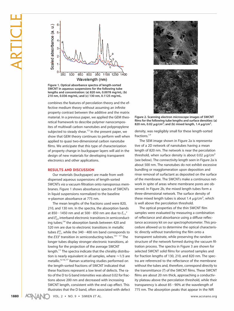
dispersed aqueous suspensions of length-sortedSWCNTs via a vacuum filtration onto nanoporous mem-branes. Figure 1 shows absorbance spectra of SWCNTsin liquid suspensions normalized to the baseline�-plasmon absorbance at 775 nm.
The mean lengths of the fractions used were 820,210, and 130 nm. In the spectra, the absorption bandsat 850�1450 nm and at 500�850 nm are due to E11
s
and E22s interband electronic transitions in semiconduct-
ing tubes;14 the absorption bands between 420 and520 nm are due to electronic transitions in metallictubes E11
m , while the 340�400 nm band corresponds tothe E33s transition in semiconducting tubes.14�17 Thelonger tubes display stronger electronic transitions, al-lowing for the projection of the average SWCNTlength.11 The spectra indicate that the chirality distribu-tion is nearly equivalent in all samples, where �1/3 aremetallic.4,16,17 Raman scattering studies performed onthe length-sorted fractions of SWCNT indicated thatthese fractions represent a low level of defects. The ra-tio of the D to G band intensities was about 0.02 for frac-tions above 200 nm and decreased with increasingSWCNT length, consistent with the end cap effect. Thisillustrates that the D band, often associated with defect
density, was negligibly small for these length-sortedfractions.17
The SEM image shown in Figure 2a is representa-tive of a 2D network of nanotubes having a meanlength of 820 nm. The network is near the percolationthreshold, when surface density is about 0.02 �g/cm2
(see below). The connectivity length seen in Figure 2a isabout 500 nm. The nanotubes do not exhibit excessivebundling or reagglomeration upon deposition andrinse removal of surfactant as deposited on the surfaceof the membrane. The SWCNTs make a continuous net-work in spite of areas where membrane pores are ob-served. In Figure 2b, the mixed length tubes form athree-dimensional network. The surface density ofthese mixed length tubes is about 1.4 �g/cm2, whichis well above the percolation threshold.
The optical properties of the thin SWCNT filmsamples were evaluated by measuring a combinationof reflectance and absorbance using a diffuse reflec-tance accessory kit on our spectrophotometer. This pro-cedure allowed us to determine the optical characteris-tic directly without transferring the film onto atransparent substrate, while preserving the randomstructure of the network formed during the vacuum fil-tration process. The spectra in Figure 3 are shown forselected SWCNT solid films for unsorted samples andfor fraction lengths of 130, 210, and 820 nm. The spec-tra are referenced to the reflectance of the membranewithout the tubes and, therefore, correspond directly tothe transmittance (T) of the SWCNT films. These SWCNTfilms are about 20 nm thick, approaching a conductiv-ity plateau above the percolation threshold, while theirtransparency is about 85�90% at the wavelength of775 nm. The absorption peaks that appear in the NIR
Figure 1. Optical absorbance spectra of length-sortedSWCNT in aqueous suspensions for the following tubelengths and concentration: (a) 820 nm, 0.0078 mg/mL; (b)210 nm, 0.036 mg/mL; and (c) 130 nm, 0.1125 mg/mL.
Figure 2. Scanning electron microscope images of SWCNTfilms for the following tube lengths and surface densities: (a)820 nm, 0.02 �g/cm2; and (b) mixed length, 1.4 �g/cm2.
ART
ICLE
VOL. 2 ▪ NO. 9 ▪ SIMIEN ET AL. www.acsnano.org1880

and in the visible range of the spectrum are character-
istic of specific tube chiralities. E11s and E22
s are due to
electronic interband transitions rising from semicon-
ducting tubes, while E11m are electronic transitions from
metallic tubes, which are similar to those shown in Fig-
ure 1 for the length-sorted nanotubes in liquid suspen-
sion. The absorption features, E11m , attributed to the me-
tallic chirality is estimated to comprise about 30% of the
sample. We note that the normalized intensities of the
absorption peaks in the films are lower than those in
suspensions shown in Figure 1 for the corresponding
tube length. The effect of decreasing intensity of the
characteristic electronic transitions in the network is
likely due to interactions between interconnecting
tubes. Diminished absorbance intensities can likewise
be attributed to doping by oxygen from the ambient at-
mosphere. These effects should be present in our films
where the protective surfactant coating has been rinsed
away. The E11s transitions are affected more strongly
than E22s .
Figure 4 shows the correlation plot between the op-
tical absorbance, a � � log(T), at the wavelength of
775 nm and surface concentration of tubes forming the
network. It demonstrates that the optical nonresonant
absorption increases nearly linearly with concentrationregardless of the tube length. A similar relationshipholds for the films made of tubes of mixed length.
By changing the concentration of SWCNTs, the sheetconductivity (�s) of our 2D networks changes by 6 or-ders of magnitude, from 10�11 S-square to about 10�5
S-square as shown in Figure 5. Our �s values obtainedfor thicker SWCNT films are in the range of about 0.001S-square, which is somewhat lower though compa-rable to the conductivity values reported for transpar-ent electrode materials made of carbonnanotubes.4,18,19 In contrast to optical absorption,which increases in linear proportion to the surface con-centration, the sheet conductivity increases dramati-cally at low concentrations and saturates above a cer-tain critical concentration. The overall character of theconductivity plots is characteristic of a percolation tran-sition. Films made of mixed length tubes show the low-est conductivities, with the percolation transition tak-ing place at higher concentration. With increasing tubelength, the network conductivity increases and the per-colation conditions for �s shift to lower concentra-tions. We also see that the crossover transition fromthe insulating to the conducting state occurs in a nar-rower concentration range. In the case of 820 nmlength tubes, the characteristic step rise in conductiv-ity takes place within a very narrow concentration rangeof about 0.008 �g/cm2.
We determined the conductivity percolation con-centration, xc, and the critical percolation exponents, sand t, in relation to the tube length by analyzing the �s
data in terms of the generalized effective mediumtheory (GEM):12
(1 - x)σi
1⁄s - σs1⁄s
σi1⁄s + Aσs
1⁄s+�
σa1⁄t - σs
1⁄t
σa1⁄s + Aσs
1⁄t) 0 (1)
where x is the tube concentration, A is a parameter re-lated to the percolation concentration, A � (1 � xc)/xc,�i � 10�11 S-square is the sheet conductivity of the in-
Figure 3. Optical reflectance of SWCNT networks for the fol-lowing tube lengths and surface densities: (a) 820 nm, 0.434�g/cm2; (b) 210 nm, 0.517 �g/cm2; (c) 130 nm, 0.564 �g/cm2; and (d) mixed length tubes, 0.455 �g/cm2.
Figure 4. Optical absorbance at 775 nm as a function sur-face concentration for length-sorted SWCNTs.
Figure 5. Conductivity as a function of surface concentra-tion for length-sorted SWCNTs. The lines represent the fit-ted conductivities to the GEM percolation model.
ARTIC
LE
www.acsnano.org VOL. 2 ▪ NO. 9 ▪ 1879–1884 ▪ 2008 1881

sulating matrix, and �a is the sheet conductivity of the
network forming conducting additive (i.e., SWCNT). The
strengths and limitations of GEM theory for describing
the conductive properties of CNTs are discussed in our
former paper,13 and we apply the method without re-
peating this discussion here. From the asymptotic char-
acter of the experimental data at high SWCNT concen-
trations, we determined �a to be in the range of 5 �
10�5 S-square. Equation 1 fits our data well, and we
then deduce xc and the percolation exponents t and s
using a nonlinear least-squares routine. The conductiv-
ity of the network in the high concentration limit is not
equivalent to that of an isolated tube.13 Rather, �a de-
pends on the contact resistance between the
CNTs20�22 and other factors4 that are not addressed in
the simple GEM model. The critical percolation param-
eters obtained from eq 1 are summarized in Table 1 for
the three different tube lengths. Interestingly, the uni-
versal percolation exponents t and s for the 820 nm and
210 nm tubes have similar values. These values are
close to those theoretically expected for a large con-
ducting 2D network,23�26 where s � t � 1.3.
Kholodenko and Freed27 argue for the exact 2D expo-
nent value, 23/18 � 1.28. Thus, we find experimental
evidence that our SWCNT networks can be described
as nearly two-dimensional and that GEM percolation
theory provides quantitative description of conductiv-
ity changes in these materials through the conductiv-
ity percolation transition. We note that the critical con-
ductivity percolation concentration that we observe
experimentally for the 820 nm tubes (xc � 0.018 �g/
cm2) is one of the smallest reported to date.
The data in Table 1 indicate that the universal perco-
lation exponents (s and t) obtained for networks made
of the shorter tubes, and especially films formed with
mixed length tubes, differ from values predicted for the
2D networks. Rather, they are found to be in accord
with those predicted by GEM theory in 3D, s � 0.8 and
t � 2.0. This indicates that an increasing fraction of
SWCNT connections are being made in the third dimen-
sion in these short tube networks.25,26,28
The variation of the percolation threshold with the
tube aspect ratio can be further understood on the ba-
sis of percolation and effective medium theory con-
cepts. A polynomial expansion of the conductivity �s
for a two-dimensional layer containing arbitrarily ori-
ented particles of fixed and identical shape relative to
an insulating layer without the particles is given by eq
229
(σs ⁄ σi) ) 1 + [σ]∞x + O(x2) (2)
where in 2D the leading virial coefficient [�] repre-
sents intrinsic conductivity of circular conducting
discs.30 Reference 29 provides results for numerous spe-
cial cases and shows that [�] for arbitrary shaped par-
ticles can be generally related to the particle transfinite
diameter. Accordingly, for an elliptic shaped particle
having aspect ratio L, [�] is given by eq 3:
[σ]∞ ) (1 + L)2 ⁄ 2L (3)
The percolation transition concentration xc can be
estimated based on the conditions that the leading cor-
rection to the conductivity becomes on the order, [�]x
� 0(1), a Ginzburg criterion.30,31 This condition, along
with eq 3, implies the general scaling relation for the
conductivity percolation concentration in 2D for slen-
der particles is
xc(slender particle) ∼ 1 ⁄ L (4)
Equation 4 suggests that, in networks exhibiting 2D
percolation transition, increasing the CNT length by a
factor of 820 nm/210 nm � 3.9 should decrease the cor-
responding percolation threshold xc by a similar factor.
Table 1 indicates that xc is indeed reduced by a factor of
4.0 in our buckypaper films, in quantitative agreement
with eq 4. In a similar fashion, xc can be predicted for
particles having arbitrary shape.31,32 Thus, we find that
the optical characteristics of the length fractionated
SWCNTs are distinct from unsorted polydisperse
SWCNTs.
Projecting the percolation conductivity plot (Figure
5) onto the linear plot of optical absorbance (Figure 4)
indicates that the direct correlation between the off-
resonant �-plasmon absorbance and the network con-
ductivity will obey the percolation model (eq 1). In par-
ticular, primarily the universal percolation exponents
will govern the optical absorbance of thin SWCNT films.
This result is quantitatively different and more univer-
sal than that adopted for SWCNTs based on the optical
properties of thin metallic films below the diffraction
limit.5,33 The characteristic electronic transitions giving
rise to chirality specific absorption bands are magnified
in longer tubes. The longer fractionated tubes are both
more transparent and conducting at the same surface
coverage. The universal percolation exponents ob-
tained for the long length tubes conform well to the
predictions of GEM percolation theory in 2D. Again, the
critical conductivity percolation concentration of 0.018
�g/cm2 in these 2D networks is the lowest reported to
TABLE 1. Percolation Parameters of SWCNT Networks inRelation to the Tube Length
tube length (nm) s t xc (�g/cm2)
820 1.25 0.4 1.35 0.1 0.018 0.01210 1.25 0.5 1.38 0.1 0.072 0.07130 1.2 0.8 1.9 0.1 0.095 0.07230 (mixed length) 0.8 0.6 2.1 0.1 0.15 0.1
ART
ICLE
VOL. 2 ▪ NO. 9 ▪ SIMIEN ET AL. www.acsnano.org1882

date. Short and mixed length tubes (Table 1) form net-works for which the universal percolation exponentsare consistent with the 3D percolation model. These ob-servations indicate that considerable control on theconductivity and optical properties can be obtained by
adjusting SWCNT length, concentration, and polydis-persity. The GEM percolation theory provides a conve-nient framework for describing and engineering thesechanges for nanotechnology applications, exploitingthese novel materials.
EXPERIMENTAL METHODSSingle-walled carbon nanotubes, SWCNTs, grown by the
cobalt�molybdenum catalyst (CoMoCat) process, were pur-chased from Southwest Nanotechnologies, Inc. (S-P95-02 grade,batch NI6-A001).1 The SWCNTs were dispersed at 1 mg soot/mLin a 2% mass fraction of sodium deoxycholate (DOC) aqueoussurfactant solution via sonication (tip sonicator, 0.64 cm, Tho-mas Scientific) for 1.5 h in an ice water bath at 1 W/mL appliedpower. Post-sonication purification was performed by centrifu-gation at an acceleration of 21 000 � 9.81 m/s2 (21 � 103 G) for2 h to pellet the non-SWCNT carbonaceous and catalyst impuri-ties. The collected supernatant contained primarily individuallydispersed SWCNTs. In order to separate the purified SWCNTs bylength, we used a dense liquid centrifugation method.11 Densitylayers were formed directly in the centrifuge tubes by layeringappropriate concentrations of iodixanol (Sigma AldrichInc.)�deoxycholate solutions such that the density of the sur-rounding medium (��layer) is larger than that of the tubes (��layer
��SWNT) in all layers. The difference in scaling with length ofthe hydrodynamic and buoyancy forces on the individualSWCNTs was then used to generate length separation underhigh acceleration. Separation was performed in a SW-32 rotor us-ing a Beckman Coulter L80 XP ultracentrifuge at 1445 rd/s for70 h. Typically, 16 individual fractions were collected after centri-fuging, by hand-pipetting in 1.5 mL increments from the top.From these, we selected three fractions having mean tubelengths of 820, 210, and 130 nm, respectively. After the lengthseparation, the SWNT mass fraction improves considerably tobetter than 95%. We also used the purified unsorted SWCNT sus-pension, which had a mean tube length of �220 nm and a stan-dard deviation of �20. However, the length distribution of thissample is approximately a log-normal and contains a broaderdistribution of tubes of varying length (mixed length fraction).This was our model polydisperse sample. Length fractions weredialyzed after separation against 0.8% DOC solution to removethe remaining iodixanol and to reduce the total surfactantconcentration.
The average length (L) of the fractionated SWCNTs was char-acterized by atomic force microscopy (AFM) and transmissionelectron microscopy (TEM) and was verified by the intensity ofthe electronic absorption peak at 984 nm on the NIR spectrum.11
The combined relative uncertainty of L mean value was approxi-mately 10%, while each fraction distribution had a standard de-viation value of about 20%.
The optical absorbance spectra of the SWCNT aqueous sus-pensions in the UV�vis�NIR range (300�1800) nm were ob-tained using a Perkin-Elmer Lambda 950 UV�vis�NIR spectro-photometer.
Fractionated SWCNTs were then deposited on the surfaceof a porous cellulose ester membrane, diameter of 47 mm, with0.05 �m diameter pore size (Millipore), via a vacuum filtrationprocess.2 The active area of the membrane surface was 10.2 cm2
(diameter 36 mm). A mixture of isopropanol and deionized wa-ter (1:4) by volume was used to “condition” the membranes andto rinse away the deoxycholate surfactant. The concentrationtubes in fractionated suspensions were typically between 0.05and 0.1 mg/mL, determined by weighing the tube deposit on amicrobalance after dialyzing and evaporating a fixed volume offractionated suspension. The networks’ surface density was con-trolled by varying the volume of the fractionated suspension us-ing a micropipette (Oxford Benchmate), then diluting the sus-pension with DI water to obtain 2 mL of dilute suspension. Thedeposited SWCNTs from the dilute suspension formed a randomnetwork on the surface of the membrane. The samples werethen dried at 50 °C for 24 h under nitrogen atmosphere. The sur-
face density of these networks was in the range of 0.01 to 2.0 �g/cm2 with the combined relative uncertainty of 30%.
The optical characteristics of the SWCNT networks were de-termined by measuring the diffuse optical reflectance in thewavelength range of 300�1800 nm, using a diffuse reflectanceaccessory kit for the Lambda 950. The reflectance spectra werenormalized to the reflectivity of the filter membrane withoutSWCNTs, which we used as a nonabsorbing reference. Thus, thespectra primarily represent the absorbance of the conductingSWCNT film.
The scanning electron microscopy images of the depositedSWCNT networks were obtained using a Hitachi S4700 field emis-sion scanning electron microscope.
To measure the electrical characteristics of the network films,an interdigitated gold electrode pattern was deposited directlyon top of the SWCNT network through a shadow mask. Electri-cal measurements were analyzed in terms of complex imped-ance, yielding the impedance magnitude (|Z*|) and the corre-sponding phase angle (�) over the frequency range of 40�10MHz by using a four-terminal fixture attached to an Agilent4294A precision impedance analyzer.13 The impedance ana-lyzer was calibrated with a standard extension adapter to short,load, and open standards. The real part (�=) of the complex sheet(surface) conductivity was determined from the measured im-pedance normalized by the geometry of the electrode pattern
σ ' ) [1 ⁄ (|Z * |cos(θ))](1 ⁄ d)
in units of (�/square)�1 or Siemens-square (S-square). Here, l isthe total length of the finger electrodes, and d is the distancebetween the fingers. In our measurements, l � 9 cm and d � 800�m. The thickness of the deposited gold electrodes was about0.1 �m. The lowest measurable sheet conductivity in oursystem was �= � 5 � 10�12 S-square at 100 Hz. The sheetconductivity of dried blank membrane substrates, withoutcarbon nanotubes, was typically below 10�11 S-square at 100Hz. The combined relative experimental uncertainty of themeasured conductivity magnitude was within 4%, while theexperimental uncertainty of the phase angle measurementswas about 0.5°. The sheet conductivity �= of our SWCNTfilms is frequency dependent but at the lowest frequenciesexhibits a plateau that persists up to crossover frequency of�s. Throughout our paper, we denote this frequencyindependent real conductivity �=(� ¡ 0, � � 0) as �s. Athigher frequencies, � �s, we observe that �= increases withincreasing frequency according to power law, �= � �n, whichis commonly described as a “universal” property ofdisordered solids and applicable to a broad range ofsemiconducting materials, conductor�dielectric mixtures,and composites.7,13
Note: Certain equipment, instruments, or materials are iden-tified in this paper in order to adequately specify the experimen-tal details. Such identification does not imply recommendationby the National Institute of Standards and Technology nor doesit imply the materials are necessarily the best available for thepurpose.
Acknowledgment. We thank Thuy Chastek for help in SEM im-aging. W.L. acknowledges support from the NIST Summer Under-graduate Research Fellowship Program.
ARTIC
LE
www.acsnano.org VOL. 2 ▪ NO. 9 ▪ 1879–1884 ▪ 2008 1883

REFERENCES AND NOTES1. Unalan, H. E.; Fanchini, G.; Kanwal, A.; Du Pasquier, A.;
Chhowalla, M. Design Criteria for Transparent Single-WallCarbon Nanotube Thin-Film Transistors. Nano Lett. 2006,6, 677–682.
2. Wu, Z. C.; Chen, Z. H.; Du, X.; Logan, J. M.; Sippel, J.;Nikolou, M.; Kamaras, K.; Reynolds, J. R.; Tanner, D. B.;Hebard, A. F.; et al. Transparent, Conductive CarbonNanotube Films. Science 2004, 305, 1273–1276.
3. Abraham, J.; Philip, B.; Witchurch, A.; Varadan, V.; Reddy,C. C. A Compact Wireless Gas Sensor Using a CarbonNanotube/PMMA Thin Film Chemiresistor. Smart Mater.Struct. 2004, 13, 1045–1049.
4. Blackburn, J. L.; Barnes, T. M.; Beard, M. C.; Kim, Y. H.;Tenent, R. C.; McDonald, J.; To, B.; Coutts, T. J.; Heben, M. J.Transparent Conductive Single-Walled Carbon NanotubeNetworks with Precisely Tunable Ratios of Semiconductingand Metallic Nanotubes. ACS Nano 2008, 2, 1266–1274.
5. Green, A. A.; Hersam, M. C. Colored SemitransparentConductive Coatings Consisting of Monodisperse MetallicSingle-Walled Carbon Nanotubes. Nano Lett. 2008, 14,1417–1422.
6. Kumar, S.; Murthy, J. Y.; Alam, M. A. PercolatingConduction in Finite Nanotube Networks. Phys. Rev. Lett.2005, 95, 066802-1–066802-4.
7. Li, J.; Ma, P. C.; Chow, W. S.; To, C. K.; Tang, B. Z.; Kim, J. K.Correlations between Percolation Threshold, DispersionState, and Aspect Ratio of Carbon Nanotubes. Adv. Funct.Mater. 2007, 17, 3207–3215.
8. Kacabas, C.; Pimparkar, N.; Yesilyurt, O.; Kang, S. J.; Alam,M. A.; Rogers, J. A. Experimental and Theoretical Studies ofTransport through Large Scale, Partially Aligned Arrays ofSingle-Walled Carbon Nanotubes in Thin Film TypeTransistors. Nano Lett. 2007, 7, 1195–1202.
9. Behnam, A.; Guo, J.; Ural, A. J. Effects of NanotubeAlignment and Measurement Direction on PercolationResistivity in Single-Walled Carbon Nanotube Films. Appl.Phys. 2007, 102, 044313-1–044313-7.
10. Rinzler, A. G.; Liu, J.; Nikolaev, P.; Huffman, C. B.; Rodriguez-Macias, F. J.; Boul, P. J.; Lu, A. J.; Heymann, D.; Colbert, D. T.;Lee, R. S.; et al. Large-Scale Purification of Single-WallCarbon Nanotubes: Process, Product, andCharacterization. Appl. Phys. A: Mater. Sci. Process. 1998, 67,29–37.
11. Fagan, J. A.; Becker, M. L.; Chun, J.; Hobbie, E. K. LengthFractionation of Carbon Nanotubes Using Centrifugation.Adv. Mater. 2008, 20, 1609–1613.
12. McLachlan, D. S.; Heiss, W. D.; Chiteme, C.; Wu, J. AnalyticScaling Functions Applicable to Dispersion Measurementsin Percolative Metal-Insulator Systems. Phys. Rev. B 1998,58, 13558–13564.
13. Obrzut, J.; Douglas, J. F.; Kharchenko, S. B.; Migler, K. B.Shear-Induced Conductor-Insulator Transition in Melt-Mixed Polypropylene-Carbon Nanotube Dispersions. Phys.Rev. B 2007, 76, 195420-1–195420-9.
14. Weisman, R. B.; Bachilo, S. M. Dependence of OpticalTransition Energies on Structure for Single-Walled CarbonNanotubes in Aqueous Suspension: An Empirical KatauraPlot. Nano Lett. 2003, 3, 1235–1238.
15. Louie, S. G. Electronic Properties, Junctions, and Defects inCarbon Nanotubes. In Carbon Nanotubes: Synthesis,Structure, Properties, and Applications; Dresselhaus, M. S.,Dresselhaus, G., Avouris, P., Eds.; Topics in Applied Physics:Springer, NY, 2000; Vol. 80; pp 113�143.
16. Jorio, A. P.; Ribeiro, H. B.; Fantini, C.; Souza, M.; Vieira,J. P. M.; Furtado, C. A.; Jiang, J.; Saito, R.; Balzano, L.;Resasco, D. E.; et al. Quantifying Carbon-Nanotube Specieswith Resonance Raman Scattering. Phys. Rev. B 2008, 72,075207-1–075207-5.
17. Yanagi, K.; Miyata, Y.; Kataura, H. Optical and ConductiveCharacteristics of Metallic Single-Wall Carbon Nanotubeswith Three Basic Colors; Cyan, Magenta, and Yellow. Appl.Phys. Express 2008, 1, 034003-1–034003-3.
18. Pelota, J.; Weeks, C.; Levitsky, I. A.; Britz, D. A.; Glatkowski,P.; Trotier, M.; Huang, T. Carbon Nanotube TransparentElectrodes for Flexible Displays. Inf. Display 2007, 2, 2–5.
19. Rowell, M. W.; Topinka, M. A.; McGehee, M. Organic SolarCells with Carbon Nanotube Network Electrodes. Appl.Phys. Lett. 2006, 88, 233506-1–233506-3.
20. Fuhrer, M. S.; Nygard, J.; Shih, L.; Forero, M.; Yoon, Y. G.;Mazzoni, M. S. C.; Choi, H. J.; Ihm, J.; Louie, S. G.; Zettl, A.; etal. Crossed Nanotube Junctions. Science 2000, 288,494–497.
21. Obrzut, J.; Migler, K.; Dong, L. F.; Jiao, J. Frontiers ofCharacterization and Metrology for Nanoelectronics; APSConf. Proceedings, 2007; Vol. 931, pp 483�485.
22. Derirda, B.; Vannimenus, J. A Transfer-Matrix Approach toRandom Resistor Networks. J. Phys. A. 1982, 15,L557–L564.
23. Clerc, J. P.; Giraud, G.; Laugier, J. M.; Luck, J. M. TheElectrical Conductivity of Binary Disordered Systems,Percolation Clusters, Fractals and Related Models. Adv.Phys. 1990, 39, 191–309.
24. Frank, D. J.; Lobb, C. J. Highly Efficient Algorithm forPercolative Transport Studies in Two Dimensions. Phys.Rev. B 1988, 37, 302–307.
25. Laugier, J. M.; Clerc, J. P.; Giraud, G.; Luck, J. M. ACProperties of 2D Percolation Networks: A Transfer MatrixApproach. J. Phys. A: Math. Gen. 1986, 19, 3153–3164.
26. Lajko, P.; Turban, L. Percolation and Conduction inRestricted Geometries. J. Phys. A: Math. Gen. 2000, 33,1683–1692.
27. Kholodenko, A. L.; Freed, K. F. Diffusion in Random Mediaas a Problem of Interacting Bose and Fermi Fields. J. Phys.A: Math. Gen. 1984, 17, L55–L59.
28. Stauffer, D. Introduction to Percolation Theory; Tayler &Francis Ltd.: London and Philadelphia, 1985.
29. Douglas, J. F.; Garboczi, E. J. Intrinsic Viscosity and thePolarizability of Particles Having a Wide Range of Shapes.Adv. Chem. Phys. 1995, 91, 85–153.
30. Dudowicz, J.; Lifschitz, M.; Freed, K. F.; Douglas, J. How FarIs Far from Critical Point in Polymer Blends? Lattice ClusterTheory Computations for Structured Monomer,Compressible Systems. J. Chem. Phys. 1993, 99, 4804–4820.
31. Bicerano, J.; Douglas, J. F.; Brune, D. A. Model for theViscosity of Particle Dispersions. J. Macromol. Sci., RevMarcomol. Chem. Phys. 1999, C39, 561–642.
32. Garboczi, E. J.; Snyder, K. A.; Douglas, J. F.; Thorpe, M. F.Geometrical Percolation of Overlapping Ellipsoids. Phys.Rev. E 1995, 52, 819–828.
33. Zhou, Y.; Hu, L.; Gruner, G. A Method of Printing CarbonNanotube Thin Films. Appl. Phys. Lett. 2006, 88, 123109-1–123109-3.
ART
ICLE
VOL. 2 ▪ NO. 9 ▪ SIMIEN ET AL. www.acsnano.org1884