STRUCTURE, SYNTHESIS, APPLICATIONS AND COMPARISON OF SINGLE WALLED AND MULTI WALLED CARBON NANOTUBES

The effect of environmental factors on the electrical conductivity of a single oligo-DNA
molecule measured using single-walled carbon nanotube nanoelectrodes
This article has been downloaded from IOPscience. Please scroll down to see the full text article.
2008 Nanotechnology 19 265704
(http://iopscience.iop.org/0957-4484/19/26/265704)
Download details:
IP Address: 202.6.242.69
The article was downloaded on 11/02/2009 at 01:44
Please note that terms and conditions apply.
The Table of Contents and more related content is available
HOME | SEARCH | PACS & MSC | JOURNALS | ABOUT | CONTACT US

IOP PUBLISHING NANOTECHNOLOGY
Nanotechnology 19 (2008) 265704 (6pp) doi:10.1088/0957-4484/19/26/265704
The effect of environmental factors on theelectrical conductivity of a singleoligo-DNA molecule measured usingsingle-walled carbon nanotubenanoelectrodesHarindra Vedala1, Somenath Roy1, Melissa Doud2, Kalai Mathee2,Sookhyun Hwang3, Minhyon Jeon3 and Wonbong Choi1
1 Nanomaterials and Device Laboratory, Department of Mechanical and MaterialsEngineering, Florida International University, Miami, FL 33174, USA2 Department of Biological Sciences, College of Arts and Science, Florida InternationalUniversity, Miami, FL 33199, USA3 Department of Nano Systems Engineering, Inje University, Gimhae 621-749, Korea
E-mail: [email protected]
Received 11 March 2008, in final form 17 April 2008Published 20 May 2008Online at stacks.iop.org/Nano/19/265704
AbstractWe present an electrical conductivity study on a double-stranded DNA molecule bridging asingle-walled carbon nanotube (SWNT) gap. The amine terminated DNA molecule was trappedbetween carboxyl functionalized SWNT electrodes by dielectrophoresis. The conductivity ofDNA was measured while under the influence of various environmental factors, including saltconcentration, counterion variation, pH and temperature. Typically, a current of tens ofpicoamperes at 1 V was observed at ambient conditions, with a decrease in conductance ofabout 33% in high vacuum conditions. The counterion variation was analyzed by changing thebuffer from sodium acetate to tris(hydroxymethyl) aminomethane, which resulted in a twoorders of magnitude increase in the conductivity of the DNA. A reversible shift in the currentsignal was observed for pH variation. An increase in conductivity of the DNA was alsoobserved at high salt concentrations.
(Some figures in this article are in colour only in the electronic version)
1. Introduction
Direct electrical characterization of DNA has recently receivedgreat attention due to its significance in various fieldsranging from biology to electronics [1–3]. Along withthe biological relevance for understanding the mechanismof DNA oxidative damage, charge transport (CT) studiesplay an important role in the technological development ofDNA microarrays, molecular switches [4] and biosensors [5].Due to the highly dynamic structure of DNA, the CT isgreatly influenced by its sequence, length and environmentalconditions, yielding several controversial results rangingfrom insulator [6], semiconductor [7] to superconductor [8].
However, experimental investigations based on electrical andelectrochemical techniques as well as theoretical studies havepartially solved the controversy of CT through DNA [9, 10].It has been shown that CT in DNA takes place via π
stacking of electron orbitals of the neighboring bases ina DNA double helix. For shorter distances the charge(hole) moves from one guanine–cytosine (GC) pair to anotherby coherent tunneling (superexchange mechanism), whereasfor longer distances thermal hopping occurs [11]. Whilemost of these results are based on indirect measurementtechniques, direct electrical characterization of a single DNAmolecule instead of a ensemble of molecules would providegreater insight in understanding the CT through this promising
0957-4484/08/265704+06$30.00 © 2008 IOP Publishing Ltd Printed in the UK1
Nanotechnology 19 (2008) 265704 H Vedala et al
biopolymer. From a technological point of view, an electronicDNA detection platform could help in eliminating the needfor amplification techniques such as the polymerase chainreaction, which is currently used for DNA sequencing andother related applications.
However, there exist several challenges in performingdirect measurements of CT through a short DNA molecule(<40 nm) [6], which include its precise manipulation, reliableinterfacing with the electrodes, electrode properties, DNA–substrate interaction and, more importantly, the environmentaleffects. Since the last decade several studies have beenperformed for understanding the electrical conductivity ofDNA molecules of various sequences and lengths rangingfrom a few nanometers to micrometers. A typicalmeasurement involves attaching the DNA molecules betweenmetal electrodes such as gold, either by direct depositionfrom the solution or by using an electric field to trap andalign the molecules [7, 12]. As the width of the electrodesis much larger than the diameter of DNA, the quantitativedetermination of the number of molecules attached betweenthe electrodes is difficult. As a result, a large variation inthe conductivity of DNA is observed in the literature. In thisrespect single-walled carbon nanotubes (SWNTs) as electrodesare a promising alternative for the electrical characterizationof single molecules. Their excellent electronic and chemicalproperties, along with the nanoscale diameter (∼2 nm)compatible with the diameter of a single DNA molecule, canbe an ideal candidate for the electrical characterization of DNAat a single molecular level. There have been a few reports onthe use of carbon nanotubes as nanoelectrodes for the electricalcharacterization of various organic molecules [13–15]. Wehave recently reported the direct electrical measurement ofa single hybridized DNA molecule using a pair of SWNTnanoelectrodes [16].
In this work, we report the influence of local environmen-tal factors on CT of a double-stranded (ds) DNA molecule atthe single molecule level. Several earlier reports have shownthe strong influence of humidity on the conductivity of DNAmolecules [17–19]. However, other environmental factors suchas counterion variation, pH and temperature, which have sub-stantial effect on DNA conductivity, were not studied in detail.Here we investigated the influence of water molecules on DNAconductivity by comparing the current–voltage (I –V ) charac-teristics measured in ambient and in high vacuum conditions.The effect of ionic variation on the electrical conductivity ofa dry DNA molecule was studied by measuring the I –V char-acteristics of dsDNA previously suspended either in sodiumacetate (NaAc) or tris(hydroxymethyl) aminomethane (TRIS).In the case of sodium acetate the counterions were Na+, whilein TRIS buffer they were H+ and NH(CH2OH)+3 [20]. The pHand temperature effect on the CT of the trapped DNA moleculewas also studied.
2. Experimental details
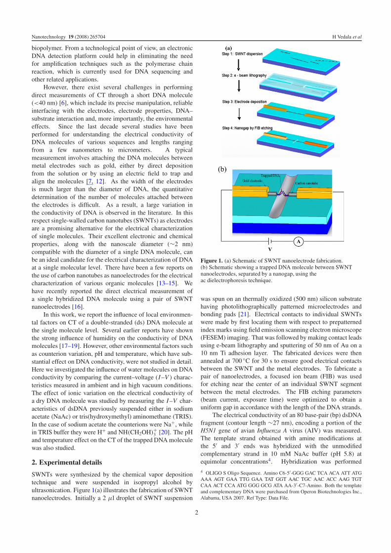
SWNTs were synthesized by the chemical vapor depositiontechnique and were suspended in isopropyl alcohol byultrasonication. Figure 1(a) illustrates the fabrication of SWNTnanoelectrodes. Initially a 2 μl droplet of SWNT suspension
Figure 1. (a) Schematic of SWNT nanoelectrode fabrication.(b) Schematic showing a trapped DNA molecule between SWNTnanoelectrodes, separated by a nanogap, using theac dielectrophoresis technique.
was spun on an thermally oxidized (500 nm) silicon substratehaving photolithographically patterned microelectrodes andbonding pads [21]. Electrical contacts to individual SWNTswere made by first locating them with respect to prepatternedindex marks using field emission scanning electron microscope(FESEM) imaging. That was followed by making contact leadsusing e-beam lithography and sputtering of 50 nm of Au on a10 nm Ti adhesion layer. The fabricated devices were thenannealed at 700 ◦C for 30 s to ensure good electrical contactsbetween the SWNT and the metal electrodes. To fabricate apair of nanoelectrodes, a focused ion beam (FIB) was usedfor etching near the center of an individual SWNT segmentbetween the metal electrodes. The FIB etching parameters(beam current, exposure time) were optimized to obtain auniform gap in accordance with the length of the DNA strands.
The electrical conductivity of an 80 base-pair (bp) dsDNAfragment (contour length ∼27 nm), encoding a portion of theH5N1 gene of avian Influenza A virus (AIV) was measured.The template strand obtained with amine modifications atthe 5′ and 3′ ends was hybridized with the unmodifiedcomplementary strand in 10 mM NaAc buffer (pH 5.8) atequimolar concentrations4. Hybridization was performed
4 OLIGO S Oligo Sequence. Amino C6-5′-GGG GAC TCA ACA ATT ATGAAA AGT GAA TTG GAA TAT GGT AAC TGC AAC ACC AAG TGTCAA ACT CCA ATG GGG GCG ATA AA-3′-C7-Amino. Both the templateand complementary DNA were purchased from Operon Biotechnologies Inc.,Alabama, USA 2007. Ref Type: Data File.
2

Nanotechnology 19 (2008) 265704 H Vedala et al
by heating the solution to 90 ◦C for 5 min followed by a2◦ decrease every 1 min, and held for 15 min at 25 ◦C,using a thermocycler. A similar hybridization protocol wasfollowed to prepare dsDNA molecules suspended in TRISbuffer [10 mM Tris-HCl/1.0 mM EDTA (pH 8.0)]. Theformation of a double helix in both the buffers, namelyNaAc and TRIS, was confirmed by a standard agarose gel-electrophoresis experiment (data not shown).
To measure the electrical conductivity of the dsDNAmolecules, the SWNT nanoelectrodes were first functionalizedwith COOH groups to form a strong covalent bond withamine terminated DNA molecule. This was performed bychemical oxidation of the SWNTs as reported in [22]. Inshort, the SWNTs were treated with HNO3 for 1 h, followedby rinsing with deionized (DI) water and vacuum drying. Thesample was then incubated for 30 min in 2 mM 1-ethyl-3-(3-dimethylaminopropyl) carbodiimide hydrochloride and 5 mMN-hydroxysuccinimide (NHS) to convert carboxyl groups toamine-reactive sulfo-NHS esters. Amine terminated dsDNAmolecules from a diluted solution (10 nM) were depositedon the electrodes and the ac dielectrophoresis technique wasused to align and immobilize the DNA molecule betweenthe electrodes (figure 1(b)). The devices were then washedwith corresponding buffer solutions to remove nonspecificallyattached DNA molecules. The samples were then blow driedwith a nitrogen stream [23]. The dielectrophoresis parameters,namely frequency (0.1–10 MHz), peak to peak voltage (0.1–5 Vpp) and time (10–500 s), were experimentally optimized.It was found that 1 MHz, 1 Vpp, for 400 s yielded higherprobability of DNA bridging the nanogap.
Control experiments such as the conductivity measure-ment of DNA-free buffers and the effect of DNAse I (diges-tion enzyme) on DNA conductivity were performed. All theI –V measurements were carried out using a four-probe stationequipped with a precision semiconductor parameter analyzer(Agilent 4156C) at ambient and in high vacuum (10−5 Torr)conditions. All measurements were made at room temperature(23 ◦C).
3. Results and discussion
Each chip consisted of several SWNT nanoelectrodes whichwere contacted by Ti/Au electrodes to micropads. Beforethe formation of a nanogap, the I –V characteristics of eachSWNT were measured. The SWNTs which exhibited metallicbehavior were selected for the fabrication of the nanogaps.Figure 2(a) shows the atomic force microscope (AFM) imageof a long SWNT which was controllably etched at adjacentlocations with gap size ranging from 20 to 30 nm, with avariation of ±3 nm. Figure 2(b) illustrates the AFM image of asingle SWNT nanoelectrode with a gap of 27 nm. Figure 3(a)depicts the I –V characteristics of a typical SWNT before andafter the etching process. The SWNT exhibited resistance inthe k� region. After FIB etching the current decreased fromseveral microamperes to a few femtoamperes (noise range ofthe instrument), indicating the nanogap formation. FIB etchingalso resulted in the formation of a trench in the oxide layerbeneath the gap. The presence of the nanotrench (width:
Figure 2. (a) Controlled etching of an SWNT dispersed on aSi/SiO2 surface using an FIB etching process. The width of thetrenches in silicon dioxide were in the range of 20–30 nm, within anerror of ±3 nm, scale bar 100 nm; (b) AFM image of SWNTnanoelectrode with an electrode separation of 30 nm,scale bar 50 nm.
27 ± 3 nm) helps in minimizing the interaction between theanchored DNA molecule and the substrate surface, whichotherwise causes a strong compression deformation of theimmobilized DNA molecule and hence a perturbation of CTthrough it [24].
As the DNA molecules are coiled in an aqueous mediumdue to thermal agitation, a strong electric field gradient isessential to straighten and attach them between the electrodes.We used ac dielectrophoresis to trap and align the DNAmolecule between the SWNT nanoelectrodes with a peak-to-peak voltage of 1 Vpp and a frequency of 1 MHz for 400 s.The applied field (40 MV m−1) is sufficiently high to overcomeBrownian motion, which is dominant in nanoscale objects [14].Figure 3(b) shows the AFM image of the DNA moleculeattached between the nanoelectrodes after dielectrophoresis.
The I –V characteristics of the double helix, hybridizedin NaAc buffer, dried and measured at ambient and in highvacuum (10−5 Torr) conditions is shown in figure 3(c). Atambient conditions a current signal of 30 pA for a 1 V biaswas observed while in high vacuum conditions the signaldecreased by 33%. This decrease may be ascribed to thepartial removal of water molecules from the proximity of theDNA. In fact, in ambient conditions the proton-transfer processin the hydration layer surrounding the DNA promotes the
3

Nanotechnology 19 (2008) 265704 H Vedala et al
Figure 3. (a) Room temperature I–V characteristics of an SWNT before and after FIB etching (30 nm gap). (b) AFM image of a single DNAmolecule trapped between a pair of SWNT nanoelectrodes. Scale bar = 30 nm. The arrow highlights the location of the trapped single DNAmolecule. (c) I–V characteristics of a dry double helix (previously suspended in NaAc) measured in ambient and in vacuum conditions. Adecrease in the signal was observed at 10−5 Torr. (d) Histogram of the current signal at 1 V bias. A total of 30 devices were measured ofwhich 20 devices showed a signal in the range 20–50 pA.
electrical conductivity but this diminishes in high vacuum [18].Figure 3(d) shows the histogram of current signal from themeasured devices. A total of 50 SWNT nanoelectrodeswith nanogaps were fabricated of which a current signal wasobtained for 30 nanoelectrodes (shown in the figure) afterbridging with the DNA molecule. After bridging the SWNTnanoelectrodes by a DNA molecule the majority of devicesexhibited a current signal in the range 20–50 pA.
Figure 4(a) shows a comparison of I –V characteristics ofhybridized DNA (in the dry state) previously suspended eitherin NaAc or TRIS buffer. A current signal in the range 25–50 pA (at 1 V bias) was observed for the DNA molecule in thecase of sodium acetate buffer. A nonlinear I –V characteristicwas observed, indicating a semiconducting behavior of thetrapped DNA fragment encoding a specific gene but devoid ofany periodic arrangement of the base pairs. In comparison,we observed that dsDNA in TRIS buffer exhibited almost twoorders of magnitude higher current. To further investigate thecause of the differences in magnitude, control experiments forboth the buffer solutions were performed. Figure 4(b) showsa comparison of I –V characteristics after spotting a dropletof DNA-free NaAc and TRIS buffer, followed by drying ina nitrogen stream. It can be seen that, after drying, TRISbuffer exhibits about two orders of magnitude higher currentas compared to that for sodium acetate. This observation
is in accordance with other recent reports wherein a largecurrent was observed for a similar control experiment withTRIS buffer [18, 25]. Hence it is apparent that, unlike sodiumacetate, the intrinsic conductivity of TRIS buffer stronglyinfluences the measured conductivity of DNA and thus can bemisinterpreted as the intrinsic conductivity of the dsDNA evenin the dry state.
The stability and conformation of DNA molecule isstrongly dependent on the ionic concentration of the buffer.Figure 4(c) demonstrates the effect of the ionic strength ofthe buffer on the DNA conductivity. It can be observedthat for buffer concentrations between 10 and 100 mM, thecurrent signal varied from 40 to 150 pA. The high currentsignal observed at higher concentrations (i.e. 100 mM) couldbe attributed to the condensation of salt residue on DNA,which might have not been removed by the washing procedurefollowed in this work. On the other hand, at very low ionconcentration (<1 mM) the current signal diminished to thefew pA region, indicating probable denaturation of dsDNA.
Figure 4(d) shows the influence of pH variation onthe conductivity of the DNA molecule. After the I –Vmeasurement of the DNA molecule at pH 5.8, the substrateswere washed with NaAc buffer (10 mM) with pH values from3.5 to 9.3 using the same experimental process mentionedearlier. It can be observed that as the pH is increased there
4

Nanotechnology 19 (2008) 265704 H Vedala et al
(b)
Figure 4. (a) I–V characteristics (in ambient conditions) of a dsDNA molecule previously suspended either in NaAc or TRIS buffer. The twoorders of higher magnitude difference in current signal observed for DNA in TRIS is attributed to the high intrinsic conductivity of the buffer;(b) control experiments showing the I–V characteristics of DNA-free NaAc and TRIS buffer measured after drying in nitrogen. In the case ofsodium acetate, only noise is observed, while for TRIS buffer current in the range of hundreds of picoamperes was observed. (c) The effect ofionic strength (NaAc) variation on DNA conductivity measured at 1 V bias. At very low ionic strength (<1 mM), the signal diminished;(d) the effect of pH variation on the conductivity of DNA measured at 1 V bias. I–V characteristics of the same device washed with buffersolution of different pH values are shown for both a gradual increase and a decrease in pH. (e) Temperature effect on DNA conductivity. Agradual increase in the device temperature resulted in a diminishing current signal. Above the melting temperature of the DNA molecule(75.6 ◦C), there was no detectable signal.
is gradual increase in the current signal. After measuring theconductivity at pH 9.3, I –V measurements were repeated bywashing the devices with buffer with descending values ofpH. The current signals were similar to the values obtainedfor the corresponding pH values during the increase of pH.A similar trend in pH dependence of DNA conductivity wasreported by Lee et al [26]. The gradual decrease in currentsignal with the lowering of the pH can be explained by the
thermal destabilization of the dsDNA molecules at extremepH values (high or low). However, this does not explain theincrease in the DNA conductivity at higher pH values observedin our measurements. Further studies have to be performedto understand the true mechanism of pH influence on DNAconductivity [27].
Figure 4(e) depicts the influence of variation oftemperature on the conductivity of the dsDNA molecule
5
Nanotechnology 19 (2008) 265704 H Vedala et al
attached between the nanoelectrodes. As the temperaturewas increased from 25 ◦C (in high vacuum) the current signaldecreased gradually. We believe that eventual evaporationof water molecules from the hydration shell surrounding theDNA molecule, and subsequent change in DNA conformation,became predominant factors in this case. Further increase intemperature above the melting temperature (TM = 75.6 ◦C)
resulted in the complete loss of signal, possibly due tothe thermal denaturation of DNA. I –V measurements aftercooling the device to room temperature yielded current in theregion of a few picoamperes(�10 pA), confirming the aboveassumption.
To confirm that the current signal was from theimmobilized DNA molecule the following control experimentwas performed. The devices were treated with DNAse Ienzyme (37 ◦C, 30 min), followed by cleaning with NaAcand DI water. DNAse I enzyme cuts the DNA regardless ofsequence. I –V measurements taken after the cleaning stepshowed no current signal (noise in the fA range), indicatingthat the current signal obtained earlier was indeed from theDNA molecule bridging the SWNT electrodes.
4. Conclusion
In conclusion, we have demonstrated that SWNTs can be ef-fectively used as nanoelectrodes to trap and electrically char-acterize a single-molecule DNA oligonucleotide. Typically, acurrent signal in the region of tens of picoamperes (for 1 Vbias) was observed for the oligo-DNA molecule (80 bp). Theinfluence of various local environmental factors on the DNAconductivity was investigated. The results show that TRISbuffer, with its high ionic conductivity, significantly affectedthe intrinsic conductivity measurement of the DNA moleculeas compared to sodium acetate, which showed negligible ef-fect. The influence of ionic strength on DNA conductivity wassignificant, especially at very high (<100 mM) concentrations,due to the condensation of salt residues. A reversible shift inthe current signal was observed for pH variation. These find-ings may shed brighter light on the ambiguities related to theelectrical properties of an oligo-DNA molecule and would fa-cilitate the development of future DNA-based nanoelectronicand sensor devices.
Acknowledgment
This work was supported in part by a Grant (FA 9550-05-1-0232) from the Air Force Office of Scientific Research, USA.
References
[1] Hall D B, Holmlin R E and Barton J K 1996 Nature 382 731[2] Fink H W and Schonenberger C 1999 Nature 398 407[3] Yoo K H, Ha D H, Lee J O, Park J W, Kim J, Kim J J, Lee H Y,
Kawai T and Choi H Y 2001 Phys. Rev. Lett. 87 198102[4] Liedl T and Simmel F C 2005 Nano Lett. 5 1894[5] Drummond T G, Hill M G and Barton J K 2003
Nat. Biotechnol. 21 1192[6] Storm A J, van Noort J, de Vries S and Dekker C 2001
Appl. Phys. Lett. 79 3881[7] Porath D, Bezryadin A, de Vries S and Dekker C 2000
Nature 403 635[8] Kasumov A Y, Kociak M, Gueron S, Reulet B, Volkov V T,
Klinov D V and Bouchiat H 2001 Science 291 280[9] Murphy C J, Arkin M R, Jenkins Y, Ghatlia N D,
Bossmann S H, Turro N J and Barton J K 1993Science 262 1025
[10] Giese B 2002 Curr. Opin. Chem. Biol. 6 612[11] Giese B, Amaudrut J, Kohler A K, Spormann M and
Wessely S 2001 Nature 412 318[12] Otsuka Y, Lee H-Y, Gu J-H, Lee J-O, Yoo K-H, Tanaka H,
Tabata H and Kawai T 2002 Japan. J. Appl. Phys. 41 891[13] Qi P, Javey A, Rolandi M, Wang Q, Yenilmez E and
Dai H 2004 J. Am. Chem. Soc. 126 11774[14] Tuukkanen S, Toppari J J, Kuzyk A, Hirviniemi L,
Hytonen V P, Ihalainen T and Torma P 2006Nano Lett. 6 1339
[15] Guo X et al 2006 Science 311 356[16] Roy S et al 2008 Nano Lett. 8 26[17] Tuukkanen S, Kuzyk A, Toppari J J, Hytonen V P,
Ihalainen T and Torma P 2005 Appl. Phys. Lett. 87 183102[18] Kleine-Ostmann T, Jordens C, Baaske K, Weimann T,
de Angelis M H and Koch M 2006 Appl. Phys. Lett.88 102102
[19] Han Ha D, Nham H, Yoo K H, So H M, Lee H Y andKawai T 2002 Chem. Phys. Lett. 355 405
[20] Stellwagen E, Dong Q and Stellwagen N C 2007Biochemistry 46 2050
[21] Kim D H, Huang J, Shin H K, Roy S and Choi W 2006Nano Lett. 6 2821
[22] Chen J, Hamon M A, Hu H, Chen Y, Rao A M, Eklund P C andHaddon R C 1998 Science 282 95
[23] Chrisey L A, Lee G U and O’Ferrall C E 1996 Nucleic AcidsRes. 24 3031
[24] Kasumov A Y, Klinov D V, Roche P E, Gueron S andBouchiat H 2004 Appl. Phys. Lett. 84 1007
[25] Zhang Y, Austin R H, Kraeft J, Cox E C and Ong N P 2002Phys. Rev. Lett. 89 198102
[26] Lee J M, Ahn S K, Kim K S, Lee Y and Roh Y 2006 Thin SolidFilms 515 818
[27] Williams M C, Wenner J R, Rouzina I and Bloomfield V A2001 Biophys. J. 80 874
6
Copyright © 2022 FDOKUMEN