Use of Raman spectroscopy in the investigation of debundling of single walled carbon nanotubes
12
Dublin Institute of Technology ARROW@DIT Conference papers Radiation and Environmental Science Centre 2005-01-01 Use of Raman Spectroscopy in the Investigation of Debundling of Single Walled Carbon Nanotubes Elizabeth Gregan Dublin Institute of Technology, [email protected] Sinead Keogh Dublin Institute of Technology T. G. Hedderman Dublin Institute of Technology Gordon Chambers Dublin Institute of Technology Hugh J. Byrne Dublin Institute of Technology, [email protected] Follow this and additional works at: hp://arrow.dit.ie/radcon Part of the Physics Commons is Conference Paper is brought to you for free and open access by the Radiation and Environmental Science Centre at ARROW@DIT. It has been accepted for inclusion in Conference papers by an authorized administrator of ARROW@DIT. For more information, please contact [email protected], [email protected]. is work is licensed under a Creative Commons Aribution- Noncommercial-Share Alike 3.0 License Recommended Citation Gregan, E., Keogh, S., Hedderman, T., Chambers, G., Byrne, H.: Use of Raman spectroscopy in the investigation of debundling of single walled carbon nanotubes. Proceedings of OptoIreland, 2005. SPIE vol. 5826, 56 (2005).
Transcript of Use of Raman spectroscopy in the investigation of debundling of single walled carbon nanotubes
Dublin Institute of TechnologyARROW@DIT
Conference papers Radiation and Environmental Science Centre
2005-01-01
Use of Raman Spectroscopy in the Investigation ofDebundling of Single Walled Carbon NanotubesElizabeth GreganDublin Institute of Technology, [email protected]
Sinead KeoghDublin Institute of Technology
T. G. HeddermanDublin Institute of Technology
Gordon ChambersDublin Institute of Technology
Hugh J. ByrneDublin Institute of Technology, [email protected]
Follow this and additional works at: http://arrow.dit.ie/radconPart of the Physics Commons
This Conference Paper is brought to you for free and open access by theRadiation and Environmental Science Centre at ARROW@DIT. It hasbeen accepted for inclusion in Conference papers by an authorizedadministrator of ARROW@DIT. For more information, please [email protected], [email protected].
This work is licensed under a Creative Commons Attribution-Noncommercial-Share Alike 3.0 License
Recommended CitationGregan, E., Keogh, S., Hedderman, T., Chambers, G., Byrne, H.: Use of Raman spectroscopy in the investigation of debundling ofsingle walled carbon nanotubes. Proceedings of OptoIreland, 2005. SPIE vol. 5826, 56 (2005).

Proceedings of OptoIreland 2005, H.J. Byrne, E. Lewis, B. D. MacCraith, E. McGlynn, J.A. McLaughlin, G.D. O'Sullivan, A.G. Ryder, J.E. Walsh eds.,SPIE vol 5826, 56 (2005)
Use of Raman Spectroscopy in the investigation of debundling of single walled carbon nanotubes
E. Gregan2*, S.M. Keogh1,2, T.G. Hedderman2, G. Chambers2, H.J. Byrne1,
FOCAS Institute1, School of Physics2, Dublin Institute of Technology, Kevin Street, Dublin 8, Ireland.
ABSTRACT
Samples of raw nanotubes are compared to those deposited from solutions to examine separation of nanotube bundles. Single wall nanotubes bundles produced by the arc-discharge and HiPco methods were solubilised in toluene, DMF and 1,2 dichloroethane. Resonant Raman spectroscopy was used to determine if debundling of the tubes sample occurred. The results showed some degree of debundling, best for the 1,2 dichloroethane solvent, which also shows long term solubility. Keywords: Carbon Nanotubes, Raman, HiPco, Arc-discharge, Debundling, Solubility
1. INTRODUCTION
Carbon nanotubes, long, thin cylinders of carbon, were discovered in 1991 by S. Iijima[1]. These are large macromolecules that are unique for their size, shape, and remarkable physical properties. These intriguing structures have sparked much excitement in the recent years and a large amount of research has been dedicated to their understanding. Carbon nanotubes are graphene sheets of sp2-bonded carbon arranged in a cylindrical formation. Single Walled Nanotubes are classified into two primary groups chiral and achiral. A nanotube is achiral if the mirror image of the nanotube has an identical structure to the original one. There are two types of achiral nanotubes; armchair and zigzag. These are formed by bisecting a C60 molecule at the equator and joining the two resulting hemispheres with a cylindrical tube one monolayer thick and with the same diameter as the C60. If the C60 molecule is bisected normal to a five-fold axis, the armchair nanotube is formed. If the C60 molecule is bisected normal to a threefold axis, the zigzag nanotube is formed. A chiral nanotube mirror image cannot be superimposed onto the original tube. Different types of nanotubes can be described by the chiral vector (n, m), where n and m are integers of the vector equation. The chiral vector is defined by [2]
Ch = na1 + ma2 (1)
An ensemble of possible chiral vectors can be specified by above equation in terms of pairs of integers (n,m) and this ensemble is shown in figure 1. The values of n and m determine the chirality, or "twist" of the nanotube. The chirality in turn affects the conductance of the nanotube, its density, its lattice structure, and other properties. For all metallic nanotubes, independent of their diameter and chirality, it follows that the density of states per unit length, N(Ef) along the nanotube axis is a constant given by[2]
taEN f
π38)( = (2)
where a is the lattice constant and |t| is the nearest neighbour carbon to carbon bond tight binding overlap energy. The equation shows the electronic 1D density of states per unit cell of a 2D metallic and semi-conducting graphene sheet.

The density of states for the nanotubes at the Fermi energy, Ef located at Ef =0, is zero for semi-conducting nanotubes, and is non-zero for metallic tubes. The energy gap Eg for semi-conducting nanotubes depends on the reciprocal of the nanotube diameter dt, which is independent of the chirality angle, and is given by[3]
tg d
CaCtE
−= . (3)
C-C=a/√3 is the nearest neighbour C-C distance on the graphene sheet. Experimental results have shown that one third of all nanotubes are conducting and the remaining two thirds are semi-conducting. At the Fermi energy (the highest occupied energy level), the density of states is finite for a metallic tube (though very small), and zero for semi-conducting tubes as mentioned before. As the energy is increased, sharp peaks in the density of states, called Van Hove singularities, appear at specified energy levels, see Fig.2.
Fig.1 Graphene layer with atoms labelled using (n,m) notation. Unit vectors of the 2D lattice

A SWNT is considered metallic if the value n - m is divisible by three. Otherwise, the nanotube is semiconducting. Consequently, when tubes are formed with random values of n and m, we would expect that two-thirds of nanotubes
ould be semi-conducting, while the other third would be metallic, which happens to be the case.
on nanotube. Given the chiral vector (n,m), the diameter of a car nanotub d relationship
w Each pair of integers (n,m) defines a different way of rolling the graphene sheet to form a carb
bon e can be determine using the
cca −3 (n + m + nm) /π2 2 1/2dt = (4)
here is the nearest-neighbour C-C distance (bond length)[2]
5 eV. Wildöer estimated it to be between 2.6 eV - 2.8 eV while at the same time, dom[4] estimated it to be 2.45 eV.
subsequent work showed that the samples were less homogeneous an originally thought. The HiPco process, high pressure CO disproportionation, has been shown to produce nanotubes
Ts had a lattice parameter of 16.52 Å and a density of 1.40 g/cm . The ace between the tubes and therefore the binding energy of the bundles is dependent on chirality and the diameter of the
of tubes were used, one produced by the arc–discharge method and one produced by the HiPco process. The diameter
cca −w Currently, the physical properties of SWNT are still being explored and disputed. What makes it so difficult is that nanotubes have a very broad range of electronic, thermal and structural properties that change depending on the different kinds of nanotube (defined by its diameter, length and chirality or twist), and this broad range potentially exists in any one sample. Nanotubes vary in size, depending on how they are produced (see later) and they aren't always perfectly cylindrical. The larger nanotubes, such as a (20, 20) tube, tend to bend under their own weight. The average bond length of 1.42 Å was measured by Spires and Brown in 1996 and later confirmed by Wildöer in 1998[3]. The C-C tight bonding overlap energy is in the order of 2.O The first
nanotubes were discovered while studying the material deposited on the cathode during the arc-evaporation synthesis of fullerenes[1]. It was found that the central core of the cathodic deposit contained a variety of closed graphitic structures including nanoparticles and nanotubes, of a type, which had never previously been observed. A short time later[5], it was shown that nanotubes could be produced in bulk quantities by varying the arc-discharge evaporation conditions. This paved the way to an explosion of research into the physical and chemical properties of carbon nanotubes in laboratories all over the world. A major event in the development of carbon nanotubes was the synthesis in 1993 of single-walled nanotubes[ 6]. The standard arc-discharge method produces only multiwalled tubes. It was found that addition of metals such as cobalt to the graphite electrodes resulted in an extremely fine tube with a single-wall. An alternative method of preparing single-walled nanotubes was described in 1995[7] . Like the original method of preparing C60, this involved the laser-vaporisation of graphite, and resulted in a high yield of single-walled tubes with unusually uniform diameters. These highly uniform tubes had a greater tendency to form aligned bundles than those prepared using arc-evaporation. Initial analysis of the tubes produced by this method showed that the samples contained a very high proportion of nanotubes with a specific armchair structure however
Fig.2: Density of States diagram, showing Van Hove singularities for a metallic and semi-conducting tube
thof high purity, with current purity of 90% atomic percent SWNT[8,9,10]. The yield and diameter size can be varied by controlling the process parameters. Another problem arises from the fact that nanotubes aggregate in bundles as a result of substantial van der Waals attractions between tubes. It has been observed that increased purity in a sample is associated with increased bundle size[11]. It is thought that there are fewer small particles present to interfere with the van der Waals attraction between neighbouring tubes. In 1996, Thess[12] measured the properties of "ropes"of carbon nanotubes. On a macroscopic scale the bundles mat together. It was found that the individual SWNTs packed into a close-packed triangular lattice with a lattice constant of about 17 Å. In addition it was concluded that the density, lattice parameter, and interlayer spacing of the ropes was dependent on the chirality of the tubes in the mat. (10, 10) Armchair tubes had a lattice parameter of 16.78 Å and had a density of 1.33 g/cm3. Zigzag tubes of the chirality (17, 0) had a lattice parameter of 16.52 Å and a density of 1.34 g/cm3. Mats made of (12, 6) chiral SWN 3
sptubes in the bundles. Armchair tubes had a spacing of 3.38 Å, zigzag tubes had a spacing of 3.41 Å, and (2n, n) chiral tubes had an interlayer spacing value of 3.39 Å. In this study comparison is made of the ability of different solvents to break up bundles of tubes. Two different samples

distribution of these sample have been previously determined to be 1.2 to 1.4 nm for arc-discharge sample and 0.7 to 1.3 nm for the HiPco sample [13][14]. Due to the higher purity it is expected that the HiPco samples will have a bigger bundle
ze than the arc-discharge tubes. In addition due to the smaller mean tube diameter the binding energy within the HiPco
d lower sides of the 580 cm line, G and G , due to the curvature of the graphene sheet. The G arises from the atomic displacements long the tube axi -
sibundles will be stronger. The average bundle size for HiPco tubes has been found to 15-30nm[15]. Raman spectroscopy has been a very useful tool in the study of carbon nanotubes for some time[2]. The Raman spectrum of a single walled tube as seen in figure 3 shows three main regions. The G-line which originates from the C=C stretching mode in graphene, shows peaks around 1580 cm-1. This peak is doubly split into higher an
-1 + - +1a s, and G , for modes with atomic displacement along the circumferential direction. Fig. 3: Stokes Raman spectrum of semiconducting nanotube taken at 633 nm with inset of
metallic nanotube G-line shape Fig. 4: Schematic picture showing the atomic vibrations for (a) G-line and (b) RBM modes

The lineshape that results is indicative of the electronic nature of the tube. The semi-conducting tube produces a G-line which is Lorentzian in shape[16][17]. In metallic tubes the −
Gω feature is broadened. This broadening is related to the presen free electrons in nanotubes with metallic character. The metallic nanotube shows a Breit-W er-Fano line shape
ce of igns sh
owever the lower com is dependant on tube diamet decreases in frequency in accordance with
[18,19]. Examination of the G-line features for isolated tube ows that the higher component +Gω is essentially
independent of tube diameter. H ponent −Gω er and
2t
GG d−= +− ωω (5)
where d
C
e tube diameter, and C=47.7cm nm for semiconducting tubes and C=79.5cm nm for metallic tubes. . h G-line for bundles also shows the two features whose spacing depends on the mean diameter of the nanotube
g the small magnitude of the BWF ffect. The BWF effect increases as the tube diameter decreases, causing the ΓG- feature to become more asymmetric and
efore e ratio of G/D line and G*/D line intensities provides a good index for showing the presence of defects decreasing with
er frequency region the spectrum is dominated by the in-phase mode known as the radial breathing mode (RBM), see figure 3. The frequency of the ersely proportional to the nanotube diameter (dt). For bundles
the spectral shift B being an empirically determined environmental dampin ctor. For isolated tubes
t is th -1 2 -1 2 [21]
Tbundle[.22]. The linewidths ΓG+ for the G peaks from isolated SWNTs are usually around 5-15cm-1, and the same range of linewidths for ΓG- are found for semiconducting isolated SWNTs [23]. For semiconducting SWNTs in bundles, the linewidths are related to the intertube interactions and to the diameter distribution. Therefore the broadening principally occurs for ΓG-. For metallic SWNTs, the broadening is minor for ΓG+ , while for ΓG- a significant broadening occurs, and it is found that the linewidth for the BWF line is strongly dependent on tube diameter. For isolated tubes with dt > 2 nm, ΓG- is similar to semiconducting SWNTs, and the line mostly looks like a normal Lorentzian, reflectinebroad. Values of ΓG- > 70 cm-1 have been observed for isolated metallic SWNTs [ 24]. The intensity of the D-line was thought until recently to be a measure of the amount of impurity in the sample. However more recently it is thought to be a measure of the level of defects along the tube itself. There is also some indication that the D-line resonance is effected by the electronic nature of the tubes[25] . It has also been shown that the D-line varies in both value and amplitude with laser excitation frequency[14]. The D-line and its second harmonic G*-line are highly dispersive and observed in isolated tubes and bundles. However in bundles superimposed on the linear dependence of ωD and ωG* on laser energy is an oscillatory feature due to resonance of the laser energy with specific van Hove singularities[24]. The D-line intensity is large compared to that of the G-line when the sample has a large number of defects while the G*-line intensities always shows a large intensity comparable to the G-line without defects. Therthincreasing order and purity[25]. The width of the D-line is smaller for semiconducting tubes than for metallic tubes. In the low
RBM (ωRBM ) is inv
g fa
tRBM d
The spectral shape and position of the Raman band associated with the RBM of the nanotubes present in a sample provide an estimate of the diameter distribution in the SWNT sample
A '' =ω
[26]. It should be noted that tubes which are most apparent in a spectrum are those which are resonantly enhanced at the wavelength employed. This is because of the one
BA+=ω (6)
dtRBM
(7)

dimensional density of states bands which are sharp and narrow. Therefore within a sample only some tubes are resonant at a given wavelength and in order to characterise fully a given sample, it is necessary to use a range of excitation frequencies. Most recently Wang et al have de
[27]veloped a method for assigning resonant scattering peaks in the
Ra an spectrum . From the radial breathing modes, data of diameters, RBM frequencies and electronic density of
gularities in isolated tubes over the spacings in bundles thereby allowing the same laser xcitation to excite different diameter tubes in the two samples[28]. The net effect of debundling is an apparent up-shift in
the Raman active RBM’s[29].
f r, a ectral resolution of 1cm per pixel is achievable. The confocal, microscopic system allows measurement of powdered
mstates have been used to graphically assign these peaks.
Lattice dynamical predictions indicate that isolated tubes should have lower ωRBM values than those in bundles.. However it has been observed that the frequencies actually upshift for single tubes in solution due to a decreased energy spacing of the Van Hove sine
2. EXPERIMENTAL
Raman measurements were taken using an Instruments S.A. Labram 1B. The Labram system is a confocal Raman imaging microscope system. Both a Helium-Neon laser (632.8nm) and an external Argon ion 514.5nm laser were used as sources. Both lasers are polarised, enabling measurement of depolarisation ratios and studies of orientation in materials. The light is imaged to a diffraction limited spot (typically 1μm) via the objective of an Olympus BX40 microscope. The scattered light is collected by the objective in a confocal geometry, and is dispersed onto an air cooled CCD array by one of two interchangeable gratings, 1800 lines/mm or 600lines/nm, allowing a range of 150cm-1 to 4000cm-1 to be covered in a single image, or with greater resolution in a combination of images. With the orme
-1spsamples with no further sample preparation. Spectral X-Y mapping may be performed with a precision of 0.1μ m. Solutions of 0.001mg/30mls tubes to solvent ratio were made using arc-discharge and HiPco tubes. This is the concentration range where nanotubes in polymer composite solutions are reported to be debundled[30]. Three different solvents, toluene, DMF and 1,2 dichloroethane(DCE) were used. The solutions were sonicated using a sonic tip for 30 seconds, allowed to settle and decanted. Samples were then made by drop casting the solutions on glass slides. Raman
ectra were the taken of these samples as well as spectra of the corresponding untreated raw tubes. The spectra were compared for changes.
ion both e arc-discharge and HiPco tubes visibly when to solution. It should also be noted that several months later the tubes
ectra va be en that although the relative amplitudes of the peaks varies in the spectra the same tubes are resonant at all times.
sp
3. RESULTS AND DISCUSSION
The first observation was the ease with which the tubes dissolved in the 1,2 dichlorethane. Even without sonicatthwere still in solution in the DCE whereas they had long since fallen out of solution in the toluene and the DMF. Spectra were obtained for a given laser line from many different points across the raw samples to see if the resulting sp ried. Most variation in the resulting spectra was observed in the RBM regions. From figure 5 below it canse
Fig 5: Stokes spectra of the RBM region for a number of spots across a HiPco sample at 514nm

The spectra for the solvent treated samples were examined. Some parameters were measured from spectra and tabulated
table 1 and table 2.
Raw Tube Toluene DMF DCE
in
Intensity G-line Solvent Sample/ Raw Sample
- 3.85 4.2 15
G-line/D-line ratio 1 1 9 11.75 0.38 .99 5.47 G*-line/D-line rat 1.77 2.21 io 2.76 2.8 ΓG (cm-1) 38 36 36 35
Raw Tube Toluene DMF DCE
Table 1: From Stokes spec am nm tra of HiPco s ples at 633
IntensityG-line Solvent Sample/ Raw Sample
- 1.1 3.0 9.9
G-line/D-line ratio 1 3 11.93 6.4 .17 2.74 G*-line/D-line ratio 0.66 9.10 0.89 4.5 ΓG (cm-1) 49 30 46 46
iggest for the CE samples and smallest for toluene. This most probably results from a dispersion of the tubes into a less compact
values these spectra show little eviation from the spectra of the raw tubes, (see figure 6), implying little debundling. So it can be concluded that in
ter of semiconducting and metallic tubes. However the treated samples this has become predominantly metallic. This would point towards the DCE having preferentially
It can be seen that for all solvents there was an increase in the intensity of the spectra for both types of tubes as evidenced in the G-line ratios above. This pattern was repeated for the 514nm spectra. The increase was b
Table 2: From Stokes spectra for arc-discharge samples at 633nm
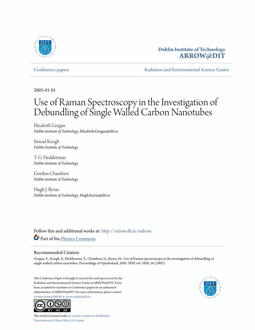
Dform. This can be simply a density effect or it could be a due to reduced damping as a result of debundling. The G/D and G*/D ratios, which are a measure of the level of order/impurity in the samples show varying results. Worth noting are the large increases in the values for the arc-discharge toluene samples. This can be explained by the effect of the toluene on dissolving tubes allowing the other impurities to precipitate resulting in a reduction in the intensity of the D-line. No such increase is seen for the HiPco tubes, consistent with their inherent purity. Notably when the spectra for both the toluene samples are examined more closely apart from changes in intensity dtoluene, bundles are solubilised, precipitating impurities, but no real debundling occurs. The spectra for arc-discharge and HiPco tubes in DCE at 633 nm are shown in figure7 and figure 8 below. In both cases there is evidence of an upshift in the spectra of the treated samples indicating some level of debundling. In the case of the HiPco tubes this is about 3-4cm-1. The profile of the RBM region in the case of the arc-discharge tubes has altered. The peaks are more distinguished and spread out indicating that the tubes are less bound together allowing greater freedom of vibration resulting in more resolution of the resonant tubes. The profile of the G-line in the arc-discharge samples has also changed. In the raw tubes it shows a mixed characindissolving the metallic tubes rather than the semiconducting tubes. In the case of the HiPco tubes, previous studies have shown little evidence of metallic tube resonances at either 633 nm or 514 nm. There is thus little change in the G-line profile in those processed with DCE (figure 8). The RBM region

similarly shows little difference to that of the raw sample. In the sample primarily consisting of semiconducting tubes, while the shift in the G-line may indicate some degree of debundling, there are few differences between the raw sample and the processed sample. The HiPco samples do however remain in solution over prolonged periods of time and thus it must be concluded that DCE dissolved the HiPco bundles. It is to be expected that due to their higher purity and smaller
iam bundles. It erefore follows that it will be easier to break up the arc-discharge bundles than the HiPco as evidenced in the spectra.
d eter size the binding within the HiPco bundles will be stronger than the binding within arc-discharge th
Fig. 7: Stokes Raman spectra for arc-discharge and DCE / arc-discharge samples at 633nm with inset of expanded RBM region
Fig. 6: Stokes Raman spectra HiPco and Toluene/ HiPco samples at 633nm
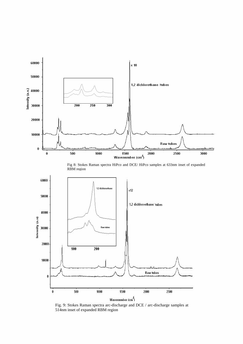
Fig 8: Stokes Raman spectra HiPco and DCE/ HiPco samples at 633nm inset of expanded RBM region
Fig. 9: Stokes Raman spectra arc-discharge and DCE / arc-discharge samples at 514nm inset of expanded RBM region

Fig. 10: Stokes Raman spectra of HiPco and DCE / HiPco samples at 514nm inset of the expanded RBM region
When the arc-discharge raw and treated samples are excited by the 514nm line (figure 9) there is no change to the profile of the G-line but again there is a significant change to the RBM’s consistant with debundling. For the HiPco at 514 nm there is some upshift in the RBM’s but not as dramatic as for the arc-discharge samples. One interesting comment on the HiPco 514 nm samples; the G-line in the raw sample although predominantly semiconducting in character shows some metallic contribution in the feature. In the DCE treated sample at 514 nm this metallic contribution seems enhanced further giving evidence to the DCE favouring metallic tubes.
−Gω
The results from anaysis of the DMF treated samples show changes in the spectra intermediate between that of the DCE and the toulene.
4. CONCLUSION
There is evidence that DMF and DCE solubilise SWNT samples and produce some degree of debundling. Toulene shows no evidence of debundling however it does purifiy the arc-discharge tubes.The results from the DCE samples show the most promise. DCE seems to solubilize both tube types easily as evidenced from visual observation. However the degree of debundling is biggest for the arc-diacharge tubes. Furthermore the there is evidence that the DCE favours metallic tubes. Further work would look at decreasing the tube to solvent ratio to see if the level of debundling can be improved. Some form of microscopy is needed to measure the actual bundle size in each of the samples which can then be matched with the measured Raman shifts. Initial investigations using AFM have showed promise.
REFERENCES [1] S.Iijima, Nature 354 , 56 (1991) [2] R.Saito, G.Dresselhaus, M.S.Dresselhaus, Physical Properties of Carbon Nanotubes, Imperial College Press, London 1998

[3] J.W.G.Wildöer, L.C.Venema, A.G.Rinzler, R.E.Smalley, and C.Dekker, Nature, 391,59(1998) [4] T.W.Odom, J.L.Huang, P.Kim and C.M.Lieber, Nature, 385, 780(1997) [5] T.W. Ebbesen and P. M. Ajayan, Nature,358, 220 (1992) [6] S. Iijima and T. Ichihashi, Nature,363, 603 (1993) [7] T.Guo, P.Nikolaev, A.Thess, R.E.Smalley Chem. Phys. Lett, 243, 49(1995) [8] H.Dai, A.G. Rinzler, P.Nikolaev, A.Thess, D.T.Colbert and R.E.Smalley Chem. Phys. Lett, 260, 471(1996) [9].W. Chiang, B.E. Brinson, A.Y. Huang, P.A. Willis, M.J. Bronikowski, R.E.Smalley J.L. Margrave and R.H. Hauge: J. Phys. B 105 , 8297-8301 (2001) [10] P. Nikolaev , M.J. Bronikowski, R. Kelley Bradley, F Rohmund, D.T. Colbert, K.A. Smith, R.E. Smalley: Chem. Phys. Lett. 313 , 91-97 (1999) [11] Strong, Anderson, Lafdi, Kuhn, Carbon 41,1477-1488 (2003) [12] Thess et al , Science 273, 483-487 (1996) [13] S.M. Keogh, T.G Hedderman, E.Gregan, G. Farrell, G. Chambers, H.J Byrne Journal of Phys. Chem. B 108 6233-6241(2004) [14] E.Gregan, S.M. Keogh, T.G. Hedderman, G. Chambers, H.J. Byrne, Facility for Optical Characterisation and Spectroscopy (FOCAS), School of Physics, Dublin Institute of Technology, Kevin Street, Dublin 8, Ireland [15]Chen, Saltiel, Manickavasagam, Schadler, Siegel, Yang, Journal of Colloid and Interface Science 208 91-97 (2004) [16] A.Jorio, G. Dresselhaus, M.S.Dresselhaus, M.Souza, M.S.Dantas, M.A. Pimenta, A.M.Rao, R.Saito, C.Liu and H.M.Cheng, Phys.Rev.Lett.85, 2617-2620 (2000) [17] S.D.M.Brown, A.Jorio, P.Corio, M.S.Dresselhaus, G. Dresselhaus, Phys.Rev.B, 63, 155414 (2001) [18] H.Kataura, Y.Kumazawa, Y.Maniwa, I.Umezu, S.Suzuki, Y.Ohtsuka and Y.Achiba Synthetic Metals, 103, 2555(1999) [19] S.D.M.Brown, A.Jorio, P.Corio, M.S.Dresselhaus, G. Dresselhaus, R.Saito, K.Kneipp, Phys.Rev.B-Rapid Comm (2001) [20] M.A.Pimenta, J.H.Hafner, C.M.Lieber, R.Saito, Phys.Rev.B 65 155412 (2002) [21] M.S.Dresselhaus, P.C.Eklund, Adv.Phys.49 705 (2000) [22] Jorio et al Phys.Rev.B 66 115411 (2002) [23] S.D.M.Brown, A.Jorio, P.Corio, M.S.Dresselhaus, G. Dresselhaus, Phys.Rev.B, 64, 073403 (2001) [24] Pimenta, Hanlon, Marucci, Corio, Browne, Empedocles, Bawendi, G.Dresselhasu, M.Dresselhaus, Brazilian J.Phys.30 423 (2000) [25] M.Dresselhaus, Jorio, Souza, G.Dresselhaus, Saito Physica B 323 15-20 (2002) [26] A.M. Rao, E. Richter, S. Bandow, B. Chase, P.C. Eklund, K.A. Williams,S.Fang, K.R. Subbaswamy, M. Menon, A. Thess, R.E. Smalley, G. Dresselhaus and M.S.Dresselhaus, Science, 275, 187 (1997). [27] Y.F.Wang, X.W Cao, S.F.Hu, Y.Y.Liu, G.X.Lan Chem.Phys.Lett.336 , 47-52 (2001) [28] Rao, Chen, Richter, Schlecht, Eklund, Haddon, Venkateswaran, Kwon, Tománek, Phys.Review Letters 86 17 (2001) [29] Duesberg et al Phys. Review Letters 85 5436 (2000) [30]Coleman, Fleming, Maier, O Flaherty, Minnett, Ferreira, Hutzler, Blau, J Phys.Chem.B.108,3446 (2004) *[email protected], phone +353 1 402 4736