Vibrational and electronic properties of single-walled and double-walled boron nitride nanotubes
13
Vibrational Spectroscopy 66 (2013) 30–42 Contents lists available at SciVerse ScienceDirect Vibrational Spectroscopy j ourna l h om epa ge : www.elsevier.com/locate/vibspec Vibrational and electronic properties of single-walled and double-walled boron nitride nanotubes Metin Aydin ∗ Department of Chemistry, Faculty of Art and Sciences, Ondokuz Mayıs University, Kurupelit, Samsun 55139, Turkey a r t i c l e i n f o Article history: Received 22 August 2012 Received in revised form 26 January 2013 Accepted 31 January 2013 Available online 9 February 2013 Keywords: SWBNNT DWBNNT Nanotube Raman IR Charge transfer IC ISC DFT calculation a b s t r a c t We calculated IR, nonresonance Raman spectra and vertical electronic transitions of the zigzag single- walled and double-walled boron nitride nanotubes ((0,n)-SWBNNTs and (0,n)@(0,2n)-DWBNNTs). In the low frequency range below 600 cm −1 , the calculated Raman spectra of the nanotubes showed that RBMs (radial breathing modes) are strongly diameter-dependent, and in addition the RBMs of the DWBNNTs are blue-shifted reference to their corresponding one in the Raman spectra of the isolated (0,n)-SWBNNTs. In the high frequency range above ∼1200 cm −1 , two proximate Raman features with symmetries of the A 1g (∼1355 ± 10 cm −1 ) and E 2g (∼1330 ± 25 cm −1 ) first increase in frequency then approach a constant value of ∼1365 and ∼1356 cm −1 , respectively, with increasing tubes’ diameter, which is in excellent agreement with experimental observations. The calculated IR spectra exhibited IR features in the range of 1200–1550 cm −1 and in mid-frequency region are consistent with experiments. The calculated dipole allowed singlet–singlet and triplet–triplet electronic transitions suggesting a charge transfer process between the outer- and inner-shells of the DWBNNTs as well as, upon irradiation, the possibility of a system that can undergo internal conversion (IC) and intersystem crossing (ISC) processes, besides the photochemical and other photophysical processes. © 2013 Elsevier B.V. All rights reserved. 1. Introduction Carbon nanotubes (CNTs) were discovered in 1991 [1], and their unique physical, chemical, and electronic properties have led to a variety of technological uses in functional nanodevices, espe- cially as transistors and sensors [2–7], in heat conduction systems [8,9], in specialty electronics [10,11], molecular memories [12], optics [13–15], electrically excited single-molecule light sources [16–19], to functionalized DNA [20,21], high-performance adsor- bent electrode material for energy-storage device [22], and protein functionalization [23,24]. In recent years there have been numer- ous experimental and theoretical studies to realize the structural and optical properties of single-walled, double-walled and multi- walled nanotubes, such as BN [25,26], BC3 [27], BC2N [28], CN [29], AlN [30] GaN [31], SiC [32], and WC [33] nanotubes, have been pre- dicted theoretically, and some of them have been synthesized, such as BN [34] and BxCyNz [35], doped and functionalized nanotubes. As it is well known, carbon nanotubes can be visualized as being formed by rolling up a defined projected area from within the hexagonal lattice of a graphene sheet in a seamless fashion such that all carbon–carbon (C–C) valences are satisfied, and the direction in which the roll up is performed transforms into the ∗ Tel.: +90 362 312 19 19x5522; fax: +90 362 457 60 81. E-mail address: [email protected] circumference of the tube. The projected area is in fact a homomor- phic representation of a particular carbon nanotube [51]. Carbon nanotubes can be metallic or semiconducting depending on their structures. This is due to the symmetry and the unique electronic structure of graphene. If the chiral indices are equal, n = m, the nanotube is metallic; if n − m is a multiple of 3, then the nano- tube is semiconducting, with a very small band gap; otherwise, the nanotube is a moderate semiconductor [36]. Interestingly, some nanotubes have conductivities higher than that of copper, while others behave more like silicon. More recently, boron nitride nanotubes (BNNTs) can be counted among the modified CNT that have been synthesized [37–39]. The electronic properties of boron nitride nanotubes differ from car- bon nanotubes: while carbon nanotubes can be either metallic or semiconducting, depending on their chirality and radius [40], all boron nitride nanotubes (BNNTs) are found to be semiconduct- ing materials with a large band gap [41,51]. In addition, since the band gap is large, the gap energy is only weakly dependent on the diameter, chirality, and the number of walls of a multi-walled tube structure. It is to be noted that single-walled and multi-walled nanotubes generally have properties that are significantly differ- ent, while double-walled nanotubes (DWNTs) can be viewed as representing the key structure that defines the transition between SWNTs and MWNTs. Moreover, because of their semiconducting character, BNNTs like CNTs themselves are also very interest- ing materials for application in nanoscale devices, and have been 0924-2031/$ – see front matter © 2013 Elsevier B.V. All rights reserved. http://dx.doi.org/10.1016/j.vibspec.2013.01.011
Transcript of Vibrational and electronic properties of single-walled and double-walled boron nitride nanotubes

Vn
MD
ARRAA
KSDNRICIID
1
uac[o[bfoawAda
btsd
0h
Vibrational Spectroscopy 66 (2013) 30– 42
Contents lists available at SciVerse ScienceDirect
Vibrational Spectroscopy
j ourna l h om epa ge : www.elsev ier .com/ locate /v ibspec
ibrational and electronic properties of single-walled and double-walled boronitride nanotubes
etin Aydin ∗
epartment of Chemistry, Faculty of Art and Sciences, Ondokuz Mayıs University, Kurupelit, Samsun 55139, Turkey
a r t i c l e i n f o
rticle history:eceived 22 August 2012eceived in revised form 26 January 2013ccepted 31 January 2013vailable online 9 February 2013
eywords:WBNNTWBNNT
a b s t r a c t
We calculated IR, nonresonance Raman spectra and vertical electronic transitions of the zigzag single-walled and double-walled boron nitride nanotubes ((0,n)-SWBNNTs and (0,n)@(0,2n)-DWBNNTs). In thelow frequency range below 600 cm−1, the calculated Raman spectra of the nanotubes showed that RBMs(radial breathing modes) are strongly diameter-dependent, and in addition the RBMs of the DWBNNTs areblue-shifted reference to their corresponding one in the Raman spectra of the isolated (0,n)-SWBNNTs.In the high frequency range above ∼1200 cm−1, two proximate Raman features with symmetries of theA1g (∼1355 ± 10 cm−1) and E2g (∼1330 ± 25 cm−1) first increase in frequency then approach a constantvalue of ∼1365 and ∼1356 cm−1, respectively, with increasing tubes’ diameter, which is in excellent
anotubeaman
Rharge transfer
CSC
agreement with experimental observations. The calculated IR spectra exhibited IR features in the rangeof 1200–1550 cm−1 and in mid-frequency region are consistent with experiments. The calculated dipoleallowed singlet–singlet and triplet–triplet electronic transitions suggesting a charge transfer processbetween the outer- and inner-shells of the DWBNNTs as well as, upon irradiation, the possibility of asystem that can undergo internal conversion (IC) and intersystem crossing (ISC) processes, besides the
phot
FT calculationphotochemical and other
. Introduction
Carbon nanotubes (CNTs) were discovered in 1991 [1], and theirnique physical, chemical, and electronic properties have led to
variety of technological uses in functional nanodevices, espe-ially as transistors and sensors [2–7], in heat conduction systems8,9], in specialty electronics [10,11], molecular memories [12],ptics [13–15], electrically excited single-molecule light sources16–19], to functionalized DNA [20,21], high-performance adsor-ent electrode material for energy-storage device [22], and proteinunctionalization [23,24]. In recent years there have been numer-us experimental and theoretical studies to realize the structuralnd optical properties of single-walled, double-walled and multi-alled nanotubes, such as BN [25,26], BC3 [27], BC2N [28], CN [29],lN [30] GaN [31], SiC [32], and WC [33] nanotubes, have been pre-icted theoretically, and some of them have been synthesized, suchs BN [34] and BxCyNz [35], doped and functionalized nanotubes.
As it is well known, carbon nanotubes can be visualized aseing formed by rolling up a defined projected area from within
he hexagonal lattice of a graphene sheet in a seamless fashionuch that all carbon–carbon (C–C) valences are satisfied, and theirection in which the roll up is performed transforms into the∗ Tel.: +90 362 312 19 19x5522; fax: +90 362 457 60 81.E-mail address: [email protected]
924-2031/$ – see front matter © 2013 Elsevier B.V. All rights reserved.ttp://dx.doi.org/10.1016/j.vibspec.2013.01.011
ophysical processes.© 2013 Elsevier B.V. All rights reserved.
circumference of the tube. The projected area is in fact a homomor-phic representation of a particular carbon nanotube [51]. Carbonnanotubes can be metallic or semiconducting depending on theirstructures. This is due to the symmetry and the unique electronicstructure of graphene. If the chiral indices are equal, n = m, thenanotube is metallic; if n − m is a multiple of 3, then the nano-tube is semiconducting, with a very small band gap; otherwise, thenanotube is a moderate semiconductor [36]. Interestingly, somenanotubes have conductivities higher than that of copper, whileothers behave more like silicon.
More recently, boron nitride nanotubes (BNNTs) can be countedamong the modified CNT that have been synthesized [37–39]. Theelectronic properties of boron nitride nanotubes differ from car-bon nanotubes: while carbon nanotubes can be either metallic orsemiconducting, depending on their chirality and radius [40], allboron nitride nanotubes (BNNTs) are found to be semiconduct-ing materials with a large band gap [41,51]. In addition, since theband gap is large, the gap energy is only weakly dependent on thediameter, chirality, and the number of walls of a multi-walled tubestructure. It is to be noted that single-walled and multi-wallednanotubes generally have properties that are significantly differ-ent, while double-walled nanotubes (DWNTs) can be viewed as
representing the key structure that defines the transition betweenSWNTs and MWNTs. Moreover, because of their semiconductingcharacter, BNNTs like CNTs themselves are also very interest-ing materials for application in nanoscale devices, and have been
Spectr
cifTtieCo
iRmcmndpetsqrroTarltt
eedrwiGsfactD
2
tsmBwittPGcnisev
M. Aydin / Vibrational
onsidered as alternatives to CNTs [42,43]. Like CNTs the mod-fication of the electronic properties of BNNTs by doping andunctionalization is an important avenue for making nanodevices.he doped BNNTs nanotubes may exhibit a dramatic change rela-ive to the pristine nanotube. Furthermore, because of the strongnteractions between electrons and holes in BNNTs [44,45], thexcitonic effects in BNNTs have proven more important than inNTs. Bright and dark excitons in BNNTs qualitatively alter theptical response [46].
As it is well known, the optical properties of nanotubes aremplicitly connected with the absorption, photoluminescence, andaman spectroscopy of nanotubes. Such optical measurements per-it a reliable characterization of the quality of nanotube such as
hirality, size, and structural defect. In the case of Raman measure-ents, even though a large number of phonon modes of carbon
anotubes would be expected, most of them are Raman inactiveue to the selection rules that emanate from the high symmetryroperties of the nanotubes. The Raman spectrum of a nanotubexhibits a few characteristic modes that can be used to determinehe size of nanotubes and to classify the type of the nanotubes,uch as semiconducting and metallic. For example, in the low fre-uency region, one type of characteristic vibration is called theadial breathing mode (RBM); this movement of the atoms is in theadial direction with the same phase, and corresponds to vibrationf the entire tube, which is strongly diameter-dependent [47,48].he RBM is used to determine the size of the nanotube. Addition-lly, there are two other characteristic Raman bands that lie in theange of 1300–1650 cm−1, which are called tangential modes. Theine shape of these Raman modes may be used to classify whetherhe nanotube is metallic or semiconducting. These Raman modes inhe high energy region are also slightly diameter dependent [47,48].
For a better understanding of the physical and optical prop-rties of nanotubes, quantum mechanical calculations have beenxtremely helpful. In this work, we provide theoretical results onouble-walled boron nitride nanotubes (DWBNNTs) using DFT; thiseport extends the quantum chemical computational approach thate have used earlier [47–49]. The results of calculations not only
ndicate the shift in the spectral peak positions of the RBM and-modes in Raman spectra of DWBNNTs relative to their corre-ponding isolated SWBNNTs, but also indicate a charge transferrom the outer-shell to the inner-shell when DWBNNTs are excited,s discussed in Section 3.4. Furthermore, the plots of the frequen-ies of vibrational radial breathing modes (RBM) versus 1/dt forhe zigzag double-walled boron nitride nanotubes (0,n)@(0,2n)-WBNNTs exhibit a strong diameter dependence.
. Computational methods
The ground state geometries of single-walled carbon nano-ubes (SWCNTs), double-walled carbon nanotubes (DWCNTs), andingle-walled boron nitride nanotubes (SWBNNTs) were opti-ized without symmetry restriction on the initial structures.
oth structure optimization and vibrational analysis calculationsere implemented using DFT with functionals, specifically, B3LYP,
n which the exchange functional is of Becke’s three parameterype, including gradient correction, and the correlation correc-ion involves the gradient-corrected functional of Lee, Yang andarr. The basis set of split valence type 6-31G, as contained in theaussian 03 software package [50], was used. The results of thealculations did not produce any imaginary frequencies. It is worthothing that during the vibrational calculations, in order to elim-
nate the contributions to the peaks intensity in the vibrationalpectra from the motion of the hydrogen atoms (on the open-nd point of the nanotube), their internal motions were fixed. Theibrational mode descriptions were made on the basis of calculated
oscopy 66 (2013) 30– 42 31
nuclear displacements using visual inspection of the animated nor-mal modes (using GaussView03) [50], to assess which bond andangle motions dominate the mode dynamics for the nanotube.The DFT method was chosen because it is computationally lessdemanding than other approaches as regards inclusion of elec-tron correlation. Moreover, in addition to its excellent accuracyand favorable computation expense ratio, the B3LYP calculationof Raman frequencies has shown its efficacy in numerous ear-lier studies performed in this laboratory and by other researchers,often proving itself the most reliable and preferable method formany molecular species of intermediate size, including anions andcations [47,48,51–56]. In our calculations, hydrogen atoms havebeen placed at the end points of the unit cells. Furthermore, thetime-dependent density functional theory at TD-B3LYP/6-31G levelwere applied to calculate the vertical electronic transitions forthe (0,n)@(0,2n)-DWCNTs and -DWBNNTs, and (0,n)- and (0,2n)-SWCNTs and -SWBNNTs.
3. Results and discussion
3.1. Structure results
Calculated diameters of the (0,n)@(0,2n)-DWCNTs (zigzagdouble-walled carbon nanotube) and (0,n)@(0,2n)-DWBNNTs(zigzag double-walled boron nitride nanotubes), for n = 6–10, werefound to decrease for the inner-nanotube and increase for theouter-nanotube, referenced to the corresponding diameter of thezigzag single-wall nanotube ((0,n)-SWNT) which changes with n. Afit to the calculated individual tube diameters for each inner- andouter-shell of the DWCNTs and DWBNNTs using a functional formthat depends inversely on single-walled nanotube’s diameter: thefitting parameters are shown in Eqs. (1a)–(2b)
Dt (outer-shell-DWCNT), in nm) = −0.040 + 0.147dt
+ 0.138
d2t
(1a)
Dt (inner-shell-DWCNT), in nm) = −0.039 + 0.037dt
+ 0.005
d2t
(1b)
Dt (outer-shell-DWBNNT), in nm) = −0.009 + 0.114dt
+ 0.143
d2t(2a)
Dt (inner-shell-DWBNNT), in nm) = −0.069 + 0.081dt
+ 0.021
d2t(2b)
A comparison of the diameters of the inner- and outer-shellsof the DWNTs with their corresponding SWNTs diameters showthat the inner-shells diameters decrease and the outer-shellsdiameters increased. These predictions explicitly indicate the exist-ence of intertube interactions in DWCNT systems. As seen inFig. 1, the diameter dependence of the curvature energies of theDWCNTs and DWBNNTs referenced to the global energies perhexagon of the (0,10)@(0,20)-DWCNTs and -DWBNNTs is wellfitted by a Lennard–Jones potential expression ELJ = −((A/r6) −(B/r12)) where parameters of the are A and B are van der Waalsinteraction parameters in Lennard–Jones potential as given in Eqs.(3a) and (3b):
�E (DWBNNTs, in eV) = −(
0.503Dt (nm)
)6{
1 −(
0.266Dt (nm)
)6}
(3a)

32 M. Aydin / Vibrational Spectr
Fig. 1. The diameter dependence of the curvature energies of the DWCNTs andDDi
�
wETddwftsbtSoNomoHsfst
((sCemstT4w
WBNNTs referenced to the global energies per hexagon of the (0,10)@(0,20)-WCNTs/DWBNNTs is well fitted by a Lennard–Jones potential expression as given
n Eqs. (3a) and (3b).
E (DWCNTs, in eV) = −(
0.477Dt (nm)
)6{
1 −(
0.356 (nm)Dt (nm)
)6}
(3b)
here �E(DWCNTs/DWBNNTs) = E[(0, n)@(0, 2n)] −[(0, 10)@(0, 2 0)] and Dt = dt(outer shell) − dt(inner shell).he results of the calculations suggest that the DWNTs with largeiameters can be much more easily formed than those with smalliameters. When comparing the formation energy of the DWCNTsith the DWBNNTs, as shown in Fig. 1, it can be seen that the
ormation of the DWBNNTs is favorable to that of DWCNTs due tohe relatively strong interactions between the inner- and outer-hells in the case of the DWBNNTs. This finding also is supportedy the calculated electron density, as discussed below, as well ashe relative change in the tube diameters when going from theWNT to the DWNT, as seen in Eqs. (1) and (2). Furthermore, ourngoing calculations on the energetically stability of the DWBN-Ts as function of the interwall distance (between inner- anduter-shells) indicate that the interwall distance around 0.34 nm isore stable, which are excellent agreement with the experimental
bservations by Cumings [57], which will be published elsewhere.owever, at different experimental conditions, the DWBNNTs with
mall interwall distance such as (0,6)@(0,12)-DWBNNT might beormed at different experimentally conditions. The DWBNNTs withmall interwall distance might be more interesting than other, inheir optical applications.
Fig. 2A and B illustrates the calculated electron density of0,6)@(0,12)-DWCNT and (0,n)@(0,2n)-DWBNNT, n = 6 and 8. For0,6)@(0,12)-DWCNT, the geometry optimization, without anyymmetry restriction, indicates a ground state point group of6v and predicted singlet-A1 electronic symmetry. The plottedlectron density showed that while first four highest occupiedolecular orbitals (from HOMO to HOMO-4, of B2, B1 and 2E2
ymmetries, respectively) involve both the inner- and outer-shell,
he HOMO-5 with the 2E1 symmetry belongs to outer-shell only.he lowest unoccupied molecular orbital, LUMO (E1) lies about.699 eV above the HOMO (B2), and belongs to the inner-shell,hile the next higher one (E1) involves not only the inner- andoscopy 66 (2013) 30– 42
outer-shell (lies 5.521 eV above the HOMO (A1)), but also a sig-nificant sigma-bonding interaction between the inner and outertubes in the excited state. For the (0,6)@(0,12)-DWCNT, the cal-culated electron density of (0,6)@(0,12)-DWCNT shows that thefirst four highest occupied molecular orbitals (from HOMO toHOMO-3, with the A1u, A2g and 2E1g symmetries, respectively)belong to the outer-shell and the next higher occupied molec-ular orbitals, from HOMO-4 to HOMO-24, include both inner-and outer-shells of (0,6)@(0,12)-DWCNT. The lowest unoccupiedmolecular orbital, LUMO (E1u) lies about 0.780 eV above the HOMO(A1u) and belongs to the outer-shell, while the next one (B2u)belongs to the inner-shell, and lies 0.849 eV above the HOMO (A1u).The calculated electron densities also indicate that an intratube(inner and outer tube) interaction may possibly take place in theexcited state, since the LUMO + 7, with A2u symmetry, is 2.494 eVabove that of the HOMO (A1u), 2.557 eV above the LUMO + 8 (E1u),2.563 eV above the LUMO + 10 (E1g), and 3.637 eV above that ofthe LUMO + 15 (E1g).
The intratube �-bonding interaction in the excited state ofthe (0,6)@(0,12)-DWBNNTs and DWCNT might lead to a probableintertube charge transfer, which can be observed by a signif-icant change in the tangential modes (TMs) in the resonanceRaman spectra when the tube excited to its intratube chargetransfer state. The TMs may not only provide information aboutthe metallic or semiconducting character of nanotubes, but alsoabout the inner-outer tube (intratube) charge transfer. Indeed, veryrecently, resonant Raman measurements [58] photoemission mea-surements, and theoretical calculations have provided evidencefor the charge transfer between the inner- and outer-shells ofDWCNTs.
Given such a scenario, small sized-DWCNTs and DWBNNTsmight be used as energy conversion systems due to charge transferbetween intershells, which might be indicated by changes in theRaman band intensities upon excitation in resonance with chargetransfer state between inner- and outer-shells.
3.2. Raman spectra of single-walled and double-walled boronnitride nanotube
We calculated Raman spectra for the zigzag single-walled boronnitride nanotube ((0,n)-SWBNNTs, n = 6–19) and double-walledboron nitride nanotube (0,n)@(0,2n)-DWBNNTs with n = 6–9. WhileFig. 3A and 4 provide the calculated Raman spectra for theSWBNNTs and DWBNNTs, respectively, Fig. 5 provides the Ramanspectra of the (0,8)@(0,16)-DWBNNT and isolated (0,8)- and (0,16)-SWBNNTs for the comparison. Furthermore, we provided thevibrational mode assignments and frequencies for the DWBNNTand isolated SWBNNTs in Table 1. All assignments to motions ofatoms or groups of atoms in Table 1 have been accomplishedthrough use of vibration visualization software (specifically,GaussView03). The results of the calculations are summarizedbelow.
Zigzag-SWBNNTs. In the low frequency region (<500 cm−1),the calculated Raman spectra of the (0,n)-SWBNNTs (n = 6–19)exhibited two Raman bands. One of them is known as the radial-breathing mode (RBM) and other is elliptical deformation mode(EDM). The RBM is an important mode for the characterization andidentification of particular nanotubes, especially of their chiralities.The importance of the radial-breathing mode for the character-ization of nanotubes derives from the inverse dependence of its
frequency on the diameter of the nanotube. As seen in Fig. 3A andB, the radial breathing mode (RBM with A1g symmetry, ωRBM(A1g))and other Raman band (elliptical deformation mode (EDM) with E2gsymmetry, ωRBM(A2g)) have frequencies that inversely depend on
M. Aydin / Vibrational Spectroscopy 66 (2013) 30– 42 33
Fig. 2. Calculated electron densities in the HOMO and LUMO states: A for the (0,6)@(0,12)-DWCNT, B for (0,6)@(0,12)-DWBNNT, C for (0,8)@(0,16)-DWBNNT, and D for(0,9)@(0,18)-DWBNNT.

34 M. Aydin / Vibrational Spectroscopy 66 (2013) 30– 42
ts of t
ad
ω
w±twtato
ω
wc
Fig. 3. (A) calculated Raman spectra of the (0,n)-SWBNNTs, n = 6–19; (B) the plo
nanotube’s diameter. A linear fit to the calculate RBM frequencyependence on nanotube diameter is provided; a linear equation:
RBM(A1g) = 48.51 + 183.54 cm−1 nmd� (nm)
,
hich is in excellent agreement with the results of the DFT within1 cm−1. However, the offset constant in the linear fitting equa-
ion (48.51 cm−1) produces significant error for the (0,n)-SWBNNTsith large diameter because the RBM decreases with increasing
ube diameter and RBM in the limit of infinite diameter yields to simple translation of the BN sheet. The RBM frequency shouldherefore go to zero in this limit. Therefore, a curve fit may bebtained using a cubic equation such as
RBM (cm−1) = 307.36 cm−1 nmdt (nm)
− 97.87 cm−1 nm2
[dt(nm)]2
+ 24.12 cm−1 nm3,
[dt(nm)]3
hich reproduces the RBMs within a ±3 cm−1 error range when,ompared with the calculated Raman spectra of the SWBNNTs from
Fig. 4. Calculated Raman spectra of the (0,n)@(0,2n)-DWBNNT, n = 0–9.
he frequencies of vibrational modes of symmetries A1g, E1g and E2g versus 1/dt .
(0,6) to (0,19) using the DFT technique and the RBM goes to zeroin the limit of infinite diameter. An analytical expression for theother accompanying calculated low frequency bands (EDM of E2gsymmetry), which has lower frequency than the RBM, the best fitparameters carried out to third order in inverse diameter parameteris given by the equation:
ωEDM(E2g) = 113.64 + 29.03 cm−1 nmdt(nm)
− 14.62 cm−1 nm2
[dt(nm)]2
+ 6.33 cm−1 nm3
[dt(nm)]3,
which reproduces exact calculated values of the EDMs. It is worthnoting that, without offset constant, fitting equation (linear orhigh order) reproduces the calculated values of the EDMs withina large error range. The band is labeled as EDM for elliptical defor-mation, which derives from the predominate motions that definevibrational mode motions, as ascertained with the vibration visu-
alization software mentioned earlier.The results of calculated Raman spectra of the (0,n)-SWBNNTsshowed that: (1) the RBM of the frequency dramatically increaseswith decreasing the SWBNNTs diameter, which is not so surprising
Fig. 5. Calculated Raman spectra of the (0,8)@(0,16)-DWBNNT and (0,8)- and (0,16)-SWBNNTs.

M. Aydin / Vibrational Spectr
Tab
le
1D
FT-c
alcu
late
d
Ram
an
vibr
atio
nal
freq
uen
cies
(in
cm−1
)
and
assi
gnm
ents
for
(0,n
)-SW
BN
NT
and
(0,n
)@(0
,2n)
-DW
BN
NTs
at
the
B3L
YP/
6-31
G
leve
l.
(0,6
)
(0,7
)
(0,8
)
(0,9
)
(0,1
0)
(0,1
1)
(0,1
2)
(0,1
3)
(0,1
4)
(0,1
5)
(0,1
6)
(0,1
7)
(0,1
8)
(0,1
9)
(0,6
)@(0
,12)
(0,7
)@(0
,14)
(0,8
)@(0
,16)
(0,9
)@(0
,18)
E 2g
167
155
147
143
139
137
135
134
133
131
130
130
129
128
246
156
206
147
170
139
152
130
Elli
pti
cal d
efor
mat
ion
(ED
M)
of
both
inn
er
and
oute
r
tube
s
in
the
sam
e
ph
ase
A1g
428
376
335
303
277
256
239
224
212
201
192
184
177
171
497
256
416
226
354
200
310
179
Rad
ial b
reat
hin
g
of
the
oute
r
tube
only
(RB
M)
A1g
826
827
826
827
827
827
827
827
827
827
827
827
827
828
820
831
823
832
823
833
823
832
Ou
t-of
-su
rfac
e
ben
din
g
def
orm
atio
n
of
the
NB
N/B
NB
bon
ds
on
the
tube
E 2g
1026
1024
1025
1026
1027
1029
1030
1031
1032
1033
1033
1034
1034
1035
1030
1027
1030
1034
BN
stre
tch
ing
(in
opp
osit
e
ph
ase)
alon
g
tube
axis
A1g
1040
1039
1040
1040
1039
1040
1040
1040
1040
1040
1039
1039
1039
1039
1040
1034
1036
1036
1039
1044
BN
stre
tch
ing
alon
g
tube
axis
only
E 2g
1181
1206
1223
1236
1244
1251
1255
1258
1261
1263
1265
1266
1267
1268
1253
1234
1206
1242
1243
1246
1238
1263
Asy
mm
etri
c
stre
tch
ing
vibr
atio
ns
and
ben
din
g
def
orm
atio
ns
of
the
BN
B/N
BN
bon
ds
E 1g
1289
1308
1320
1329
1335
1340
1344
1347
1349
1351
1353
1354
1356
1356
1351
1341
1352
Ben
din
g
def
orm
atio
n
of
the
NB
N/B
NB
bon
ds,
incl
ud
ing
rela
tive
ly
wea
k
BN
bon
d
stre
tch
ing
A1g
1333
1343
1349
1353
1355
1358
1360
1361
1362
1363
1363
1364
1364
1365
1371
1368
1358
1363
BN
stre
tch
ing
and
ben
din
g
def
orm
atio
n
of
the
NB
N/B
NB
bon
ds
alon
g
tube
axis
E 1g
1370
1355
1382
1401
1413
1419
1419
1418
1416
1414
1412
1410
1408
1406
1366
1398
1373
1376
Asy
mm
etri
c
stre
tch
ing
vibr
atio
ns
and
ben
din
g
def
orm
atio
ns
of
the
BN
B/N
BN
bon
ds.
E 2g
1399
1393
1407
1414
1417
1424
1432
1437
1441
1444
1443
1446
1447
1446
1420
1429
BN
stre
tch
ing
and
ben
din
g
def
orm
atio
ns
of
NB
N/B
NB
bon
ds
E 1gE 2
g14
42
1436
1461
1476
1486
1492
1495
1495
1499
1499
1501
1502
1503
1504
1413
1432
1434
1434
BN
stre
tch
ing,
incl
ud
ing
ben
din
g
def
orm
atio
ns
of
NB
N/B
NB
bon
ds
A1g
1481
1490
1496
1500
1502
1504
1505
1507
1507
1508
1509
1509
1509
1510
1430
1511
1463
1517
1473
1517
1485
1519
BN
stre
tch
ing
alon
g
tube
axis
, in
clu
din
g
ben
din
g
def
orm
atio
ns
of
NB
N/B
NB
bon
ds
oscopy 66 (2013) 30– 42 35
since the N B N bond strain and the sp3 hybridization rapidlyincreases with decreasing SWBNNTs diameter; (2) as seen in Fig. 3,for large-sized SWBNNTs, the ωRBM(A1g) and ωEDM(E2g) modefrequencies converge. For instance, the calculated frequency sep-aration between the RBM and EDM is found to be 3, 7, 21 and43 cm−1, when n has the values 26, 25, 22 and 19, respectively.Thus, one can anticipate that the (0,28)-SWBNNT would have unre-solvable RBM and EDM bands for the experimental spectra. Wecan anticipate that the acquisition of Raman spectra for exper-imental samples consisting of large diameter SWBNNT with thepurpose of characterizing the sample in terms of electronic prop-erties and purity may be complicated by the existence of this EDMband, which, in general, can lead to apparent broadening of bands aswell as the presence of additional bands that may lead to the erro-neous conclusion that more than one type of SWBNNT is presentin the sample. Of course, this issue is not expected to be of greatsignificance since the synthesis routes that are presently in voguedo not lead to nanotubes with diameter as large as that corre-sponding to the (0,26) index. It is to be noted that the E2g bandhas lower frequencies than the RBM (see Fig. 3A). This latter bandis labeled as EDM for elliptical deformation, which derives fromthe predominate motions that define vibrational mode motions, asascertained with the vibration visualization software mentionedearlier.
As regards other general conclusions that can be drawn fromour calculations for the SWBNNTs, we have found that cal-culated Raman bands in the mid-frequency region exit nearlysize-independent peak positions. As shown in Table 1 or Fig. 3Aand B, in the high frequency region there are a few Raman bands ofsymmetries E1g/E2g/A1g that lie close to one another in frequency.For instance, the calculated Raman modes with symmetries of theA1g (∼1355 ± 10 cm−1) and E2g (∼1330 ± 25 cm−1) approach oneanother in frequency with increasing diameter of the SWBNNTand then reach a constant values of 1365 and 1356 cm−1, respec-tively, as seen in Table 1. A fitting equation indicated that these twoRaman bands (with symmetries A1g at ∼1355 ± 10 cm−1 and E2g(∼1330 ± 25 cm−1) first increase in frequency then approach a con-stant value of ∼1366 and ∼1360 cm−1, respectively, with increasingdiameter of the (0,n)-SWBNNT, n = 25. Furthermore, the resonanceRaman experiments [59,60] have been shown that there is onlyone strong band at 1355 ± 10 cm−1 in high energy region for theboron nitride nanotubes. Thus, these calculated Raman bands atA1g (∼1355 ± 10 cm−1) and E2g (∼1330 ± 25 cm−1) are not only ingood agreement with experiments, but also suggest that only theRaman band(s) (of the symmetry of A1g and/or E2g) are theatricallyenhanced by resonance excitation of the boron nitride nanotube.
Furthermore, the predicted shifts in the peak positions mayresult from the nanotube curvature effect as mentioned in Refs.[47–49], the curvature energy of the nanotube brings about dissim-ilar force constants along the nanotube axis and the circumferencedirection. Therefore, the nanotube geometry causes a constantforce reduction along the tube axis compared to that in the cir-cumferential direction. Consequently, the curvature effect mightplay crucial role in the shift of the peak positions of the G-band aswell as the RBM band, as mentioned earlier. In addition, the cal-culated Raman band positions for bands at ∼1240 ± 30 cm−1 arefound to be slightly size dependent, exhibiting a slightly blue shiftwith increasing diameter of the SWBNNTs. This disorder inducedmode is also important for the characterization and the defect onthe nanotube as observed a broad feature around in the spectrumof the Al-modified MWBNNTs [62]. For example, in the resonanceRaman enhanced spectrum, the relative intensity of the disorder
mode increases relative to the intensity of the breathing and tan-gential modes since there is a defect on the nanotube surface as aresult of chemical functionalization or caused by structural defor-mation. For the carbon nanotubes (CNTs), the experimental studies
36 M. Aydin / Vibrational Spectr
FD
hcnba
rnatciGfabttFeDotissS2tS4(ocFDRS
ig. 6. Calculated molecular motions for some vibrational bands of the (0,8)@(0,16)-WBNNTs and (0,8)- and (0,16)-SWBNNTs.
ave showed that the increase in the intensity ratio (ID/IG) indi-ates an increase in the number of defects on the sidewall of theanotube. This is expected result of the introduction of covalentlyound moieties to the nanotube framework, in which significantmount of the sp2 carbons is converted to sp3 hybridization.
Zigzag-DWBNNTs. While Fig. 4 provides the calculated non-esonance Raman spectra for the (0,n)@(0,2n)-DWBNNTs, with
ranging from 6 to 9; Fig. 6 provides diagrams of thetomic motions associated with the vibrational frequencies forhe (8,0)@(16,0)-DWBNNT used as a representative case. Thealculations show that the frequencies of the radial breath-ng modes (RBMs) and tangential modes (TMs, known as-mode) of (n,0)@(2n,0)-DWBNNT (with n = 6–9) significantly dif-
er from those calculated for the (0,n)-SWBNNTs (see Fig. 5nd Table 1). The results of the calculations are summarizedelow. In the low frequency region, the calculated Raman spec-ra of these DWBNNTs exhibited two RBM modes resulting fromhe radial motion of the inner- and outer-shells, as shown inig. 4, and both of these RBM modes are strongly diameter depend-nt. A large gap between RBMs in the Raman spectra of theWBNNTs decreases with increasing diameter of the inner- anduter-shells (as seen in Fig. 4). Comparing these calculated RBMs inhe spectrum of the (0,8)@(0,16)-DWBNNT with their correspond-ng bands in the isolated (0,8)- and (0,16)-SWBNNTs spectra, aseen in Fig. 5, we note that the RBMs at 335 cm−1 in the Ramanpectrum of the (8,0)-SWBNNT and at 192 cm−1 in the (16,0)-WBNNT spectrum are, respectively, upward shifted to 354 and00 cm−1 in the spectrum of (0,8)@(0,16)-DWBNNT. Additionally,he RBMs for the (0,6)-SWBNNT (428 cm−1) and for the (0,12)-WBNNT (239 cm−1) spectrum are, respectively, blue shifted to97 and 256 cm−1 in the Raman spectrum of (0,6)@(0,12)-DWBNNTsee Table 1). The relative distances between RBMs in the spectraf (0,n)@(0,2n)-DWCNTs are greater than the separation betweenorresponding RBMs in Raman spectra of (0,n)- and (0,2n)-SWCNTs.
or instance, the distance between the RBMs for (0,8)@(0,16)-WBNNT is 154 cm−1, this distance between the RBMs in theaman spectra of the corresponding isolated (0,8)- and (0,16)-WBNNTs is 143 cm−1. A tentative fitting equation may be obtainedoscopy 66 (2013) 30– 42
as given in Eqs. (4a) and (4b):
ωinner(RBM, in cm−1) = 181.27dt (nm)
+ 37.00
[dt (nm)]2− 4.82
[dt (nm)]3
(4a)
ωouter (RBM, in cm−1) = 237.34dt (nm)
+ 65.65
[dt (nm)]2− 51.85
[dt (nm)]3
(4b)
where dt stand for the shell diameter. The tentative fitting equa-tions reproduced calculated RBMs within 0.5 cm−1 error range forboth inner- and outer-tubes. Another Raman bands below RBMmodes in the spectra of the SWBNNTs are blue-shifted relativeto the corresponding peaks in the spectra of their correspondingDWBNNTs. For instance, these Raman features at 147 cm−1 in thespectra of (0,8)-SWBNNT and at 130 cm−1 in the spectrum of the(0,16)-SWBNNT are respectively blue-shifted to 170 and 139 cm−1
in the spectrum of the (0,8)@(0,16)-DWBNNT. Furthermore, in themid-frequency region, the relatively weak intense peaks are cen-tered 1036 (A1g), 1030 (E2g) and 823 (A1g) cm−1 are predictedalmost at the same positions in the spectra of both (0,8)- and (0,16)-SWBNNTs.
In the high frequency region, comparing the Raman features inthe spectra of the (0,8)@(0,16)-DWBNNTs with their band positionin the corresponding (0,n)-SWBNNTs spectra, it can be seen thatthey are slightly shifted relative to SWBNNTs, as seen in Fig. 5 for the(0,8)@(0,16)-DWBNNT. For instance, the Raman bands at 1434 (A1g,relatively weak), 1420 (E1g, medium intense), 1373 (E1g, the moststronger one), 1358 (A1g, relatively weak), and 1246 (E1g, relativelystrong) cm−1 in the spectrum of the (0,8)@(0,16)-DWBNNT corre-spond to the Raman features at 1461 (medium), 1407 (medium),1382 (medium), 1349 (medium), and 1223 (the most stronger)cm−1 in the spectrum of the (0,8)-SWBNNT, and these are pre-dicted at 1501 (relatively weak), 1443 (medium), 1412 (the moststronger), 1363 (relatively weak), and 1265 (relatively strong) cm−1
in the spectrum of the (0,16)-SWBNNT (see Fig. 4), respectively.Moreover, Bando [61] has studied Raman spectra of the multi-
walled boron (natural 11B and isotope 10B) nitride nanotubes(MWBNNT and MW10BNNT). Their Raman spectra of the MWBNNTand MW10BNNT showed only one strong Raman peak at 1366 and1390 cm−1, respectively, in the range of 1200–1500 cm−1, whichis assigned to a BN stretching deformation vibration mode. Thismeasured Raman peak is in good agreement with our calculatedRaman peaks at 1373 (E1g) in the calculated nonresonance Ramanspectrum of the (0,8)@(0,16)-DWBNNT, which has resulted fromthe BN stretching along tube axis, including bending deformationof the NBN/BNB bonds along tube axis. Additionally, Obraztsova[62] has studied a comparative Raman spectra of the multi-walledboron nitride nanotubes (MWBNNTs) samples before and afterAl ion modifications have been investigated. Two features in theRaman spectra were observed: one at 1366 cm−1 that correspondsto in-plane vibrations between B and N atoms and broad featurearound 1293 cm−1 in the spectrum of the Al-modified MWBNNTs.The broad peak around 1293 cm−1 is consistent with the calculatedRaman feature around 1250 cm−1 in the spectra of the DW- andSW-BNNTs.
3.3. IR spectra of single-walled and double-walled boron nitridenanotube
Zigzag-SWBNNTs. Fig. 7A provides calculated IR spectra for the
(n,0)-SWNTs, where n ranges from 6 to 19. As evidenced in Fig. 7,the calculated IR spectra exhibited seven peaks of symmetries E1uand A1u are slightly depend on the SWBNNTs diameter. In therange of 1000–1550 cm−1, relatively very weak six IR features of
M. Aydin / Vibrational Spectroscopy 66 (2013) 30– 42 37
and (B) the plots of the frequencies of vibrational modes versus 1/dt .
s∼csqecob
ω
wa−−11c(pfacimvmz
fpis(a1ctB(
Fig. 8. Calculated IR spectra of the (0,n)@(0,2n)-DWBNNT, n = 0–9.
Fig. 7. (A) calculated IR spectra of the (0,n)-SWBNNTs, n = 6–19
ymmetries E1u are centered: ∼1475 ± 25, ∼1330 ± 30, ∼1230 ± 30,1030 ± 5 cm−1, and other two weak peaks with symmetry A1u are
entered ∼1495 ± 15 and ∼1350 ± 15 cm−1. The strongest one withymmetry E1u is centered 1395 ± 30 cm−1. In the range of mid fre-uency, the calculated IR spectra of the (0,n)-SWBNNTs (n = 6–19)xhibited only one weak peak centered 805 ± 15 cm−1. The analyti-al expressions for this calculated high frequency band as functionsf third order in inverse of the (0,n)-SWBNNTs diameter are giveny the equations:
(cm−1) = A + B
dt (nm)+ C
[dt (nm)]2+ D
[dt (nm)]3
here the parameters A (in cm−1), B (in cm−1 nm), C (in cm−1 nm2)nd D (in cm−1 nm3) are respectively obtained such as: 1508.9, 10.3,15.6, and 2.4 for the peak (A1u) centered 1495 ± 15 cm−1; 1515.7,14.9, −2.4, and −3.6 for the peak (E1u) centered 1475 ± 25 cm−1;344.7, 130.0, −54.1, and −2.4 for the peak (E1u) centered395 ± 30 cm−1; 1357.2, 33.7, −41.0, and 10.2 for the peak (A1u)entered 1350 ± 15 cm−1; 1367.0, −4.9, −17.4, and 0.8 for the peakE1u) centered 1330 ± 30 cm−1; 1264, 23.2, −37.3, and 3.8 for theeak (E1u) centered 1230 ± 30 cm−1; 1030.5, 28.6, −31.4, and 9.1or the peak (E1u) centered 1030 ± 5 cm−1; and 824.8, 7.5, −22.3,nd 4.1 for the peak (E1u) centered 805 ± 15 cm−1. The plots of thealculated IR features versus inverse of the tube diameter are givenn Fig. 7B. In the low frequency region, the IR spectra exhibited
any IR features; however, their intensities are extremely weak oranish as seen in Fig. 7A. Furthermore, we provided the vibrationalode assignments and frequencies for the IR spectra of the isolated
igzag-SWBNNTs in Table 2.Zigzag-DWBNNTs. While Fig. 8 provides the calculated IR spectra
or the (0,n)@(0,2n)-DWBNNTs, with n ranging from 6 to 9; Fig. 9rovides calculated IR spectra of the (0,8)@(0,16)-DWBNNTs and
solated (0,8)- and (0,16)-SWBNNTs for comparison. The calculatedpectra of the DWBNNTs 1517 (A1u), 1474 (E1u), 1434 (E1u), 1373E1u), 1347 (A1u), 1238 (E1u), 823 (E1u) and 786 (E1u) cm−1, whichre correspond the IR features at 1496, 1473, 1407, 1320, 1349,224, and 798 cm−1 in the spectrum of the (0,8)-SWBNNT; these are
alculated at 1509, 1501, 1412, 1353, 1363, 1261, and 819 cm−1 inhe spectrum of the (0,16)-SWBNNT, as seen in Table 2. Moreover,ando [61] have studied FTIR spectra of the multi-walled boronnatural 11B and isotope 10B) nitride nanotubes (MWBNNT andFig. 9. Calculated IR spectra of the (0,8)@(0,16)-DWBNNT and (0,8)- and (0,16)-SWBNNTs for comparison.
38 M. Aydin / Vibrational Spectr
Tab
le
2D
FT-c
alcu
late
d
IR
vibr
atio
nal
freq
uen
cies
(in
cm−1
)
and
assi
gnm
ents
for
(0,n
)-SW
BN
NT
and
(0,n
)@(0
,2n)
-DW
BN
NTs
at
the
B3L
YP/
6-31
G
leve
l.
(0,6
)
(0,7
)
(0,8
)
(0,9
)
(0,1
0)
(0,1
1)
(0,1
2)
(0,1
3)
(0,1
4)
(0,1
5)
(0,1
6)
(0,1
7)
(0,1
8)
(0,1
9)
(0,6
)@(0
,12)
(0,7
)@(0
,14)
(0,8
)@(0
,16)
(0,9
)@(0
,18)
E 1u
788
793
798
804
807
811
813
815
817
818
819
820
821
821
764
813
775
820
786
823
795
824
Ou
t-of
-su
rfac
e
ben
din
g
def
orm
atio
n
of
the
NB
N/B
NB
bon
ds
on
the
tube
E 1u
1182
1207
1224
1235
1242
1248
1252
1255
1258
1260
1261
1262
1264
1264
1253
1197
1238
1257
Asy
mm
etri
c
stre
tch
ing
vibr
atio
ns
of
the
NB
N/B
NB
bon
ds
du
e
to
the
mot
ion
s
of
the
N
and
B
atom
s
alon
g
circ
um
fere
nce
dir
ecti
on.
E 1u
1298
1308
1320
1329
1335
1340
1344
1347
1349
1351
1353
1354
1356
1356
1366
1351
1373
1376
Ben
din
g
def
orm
atio
n
of
the
NB
N/B
NB
bon
ds,
incl
ud
ing
rela
tive
ly
wea
k
BN
bon
d
stre
tch
ing
A1u
1333
1343
1349
1353
1355
1358
1359
1361
1362
1363
1363
1364
1364
1365
1332
1332
1347
1363
BN
stre
tch
ing
and
ben
din
g
def
orm
atio
n
of
the
NB
N/B
NB
bon
ds
alon
g
tube
axis
E 1u
1370
1394
1407
1414
1418
1419
1419
1418
1416
1414
1412
1410
1408
1406
1439
1433
1434
1429
Asy
mm
etri
c
stre
tch
ing
vibr
atio
ns
and
ben
din
g
def
orm
atio
ns
of
the
BN
B/N
BN
bon
ds.
E 1u
1442
1462
1473
1481
1486
1491
1493
1496
1498
1499
1501
1502
1503
1504
1488
1466
1474
1476
BN
stre
tch
ing,
incl
ud
ing
ben
din
g
def
orm
atio
ns
of
NB
N/B
NB
bon
ds
A1u
1481
1490
1496
1500
1502
1504
1505
1507
1507
1508
1509
1509
1509
1510
1511
1517
1517
1519
BN
stre
tch
ing
alon
g
tube
axis
, in
clu
din
g
ben
din
g
def
orm
atio
ns
of
NB
N/B
NB
bon
ds
oscopy 66 (2013) 30– 42
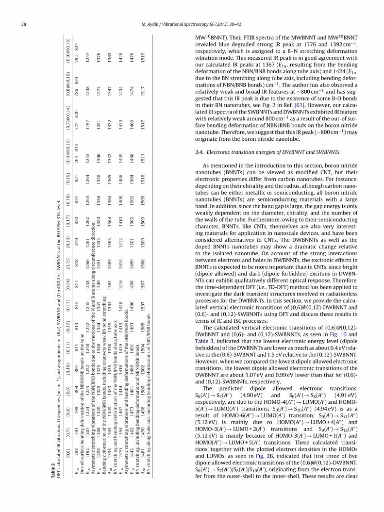
MW10BNNT). Their FTIR spectra of the MWBNNT and MW10BNNTrevealed blue degraded strong IR peak at 1376 and 1392 cm−1,respectively, which is assigned to a B–N stretching deformationvibration mode. This measured IR peak is in good agreement withour calculated IR peaks at 1367 (E1u, resulting from the bendingdeformation of the NBN/BNB bonds along tube axis) and 1424 (E1u,due to the BN stretching along tube axis, including bending defor-mations of NBN/BNB bonds) cm−1. The author has also observed arelatively weak and broad IR features at ∼800 cm−1 and has sug-gested that this IR peak is due to the existence of some B-O bondsin their BN nanotubes, see Fig. 2 in Ref. [61]. However, our calcu-lated IR spectra of the SWBNNTs and DWBNNTs exhibited IR featurewith relatively weak around 800 cm−1 as a result of the out-of sur-face bending deformation of NBN/BNB bonds on the boron nitridenanotube. Therefore, we suggest that this IR peak (∼800 cm−1) mayoriginate from the boron nitride nanotube.
3.4. Electronic transition energies of DWBNNT and SWBNNTs
As mentioned in the introduction to this section, boron nitridenanotubes (BNNTs) can be viewed as modified CNT, but theirelectronic properties differ from carbon nanotubes. For instance,depending on their chirality and the radius, although carbon nano-tubes can be either metallic or semiconducting, all boron nitridenanotubes (BNNTs) are semiconducting materials with a largeband. In addition, since the band gap is large, the gap energy is onlyweakly dependent on the diameter, chirality, and the number ofthe walls of the tube. Furthermore, owing to their semiconductingcharacter, BNNTs, like CNTs, themselves are also very interest-ing materials for application in nanoscale devices, and have beenconsidered alternatives to CNTs. The DWBNNTs as well as thedoped BNNTs nanotubes may show a dramatic change relativeto the isolated nanotube. On account of the strong interactionsbetween electrons and holes in DWBNNTs, the excitonic effects inBNNTs is expected to be more important than in CNTs, since bright(dipole allowed) and dark (dipole forbidden) excitons in DWBN-NTs can exhibit qualitatively different optical response. Therefore,the time-dependent DFT (i.e., TD-DFT) method has been applied toinvestigate the dark transient structures involved in radiationlessprocesses for the DWBNNTs. In this section, we provide the calcu-lated vertical electronic transitions of (0,6)@(0,12)-DWBNNT and(0,6)- and (0,12)-SWBNNTs using DFT and discuss these results interms of IC and ISC processes.
The calculated vertical electronic transitions of (0,6)@(0,12)-DWBNNT and (0,6)- and (0,12)-SWBNNTs, as seen in Fig. 10 andTable 3, indicated that the lowest electronic energy level (dipoleforbidden) of the DWBNNTs are lower as much as about 0.4 eV rela-tive to the (0,6)-SWBNNT and 1.5 eV relative to the (0,12)-SWBNNT.However, when we compared the lowest dipole allowed electronictransitions, the lowest dipole allowed electronic transitions of theDWBNNT are about 1.07 eV and 0.99 eV lower than that for (0,6)-and (0,12)-SWBNNTs, respectively.
The predicted dipole allowed electronc transitions,S0(A′) → S7(A′′) (4.90 eV) and S0(A′) → S8(A′′) (4.91 eV),respectively, are due to the HOMO-4(A′′) → LUMO(A′) and HOMO-5(A′) → LUMO(A′) transitions; S0(A′) → S10(A′′) (4.94 eV) is as aresult of HOMO-6(A′′) → LUMO(A′) transition; S0(A′) → S11(A′′)(5.12 eV) is mainly due to HOMO(A′′) → LUMO + 4(A′′) andHOMO-3(A′) → LUMO + 2(A′) transitions and S0(A′) → S12(A′′)(5.12 eV) is mainly because of HOMO-3(A′) → LUMO + 1(A′′) andHOMO(A′′) → LUMO + 5(A′) transitions. These calculated transi-tions, together with the plotted electron densities in the HOMOs
and LUMOs, as seen in Fig. 2B, indicated that first three of fivedipole allowed electronic transitions of the (0,6)@(0,12)-DWBNNT,S0(A′) → S7(A′′)/S8(A′)/S10(A′), originating from the electron trans-fer from the outer-shell to the inner-shell. These results are clear
M. Aydin / Vibrational Spectroscopy 66 (2013) 30– 42 39
Table 3The calculated vertical electronic transitions, singlet–singlet (S0 → Sn and triplet–triplet (T1 → Tn), of the (12,0)&(6,0)-DWBNNT and (12,0)- and (6,0)-SWBNNTs for comparisonat the B3LYP/6-31G level of using DFT. Note that the SCF corrected triplet–triplet electronic transitions were calculated as the deference between the calculated global energiesof the singlet and triplet sates added to triplet–triplet electronic transitions in order to comparing with the singlet–singlet transitions and where the letters S0, T1 and f arerespectively the lowest energy level of the singlet, triplet states and oscillator strength.
Exc. St.# (0,6)@(0,12)-DWBNNT (0,12)-SWBNNT (0,6)-SWBNNT
S0 → Sn T1 → Tn (SCF corrected) S0 → Sn S0 → Sn
Sym. eV f Sym. eV f Sym. eV f Sym. eV f
1 A′′ 4.35 A′′ 4.24 E1 5.83 A′′ 4.722 A′ 4.47 A′ 4.59 0.0071 E1 5.95 A′ 4.863 A′′ 4.67 A′′ 4.59 0.0072 E1 5.95 A′′ 4.864 A′ 4.67 A′′ 4.93 0.0006 E1 5.97 0.0871 A′ 4.865 A′ 4.89 A′ 4.93 0.0007 E1 5.97 0.0871 A′′ 5.716 A′′ 4.89 A′ 4.96 E1 6.01 0.0239 A′ 5.717 A′′ 4.90 0.0334 A′′ 4.96 E2 6.19 A′ 5.838 A′ 4.91 0.0331 A′′ 4.98 E2 6.19 A′ 5.89 0.00019 A′ 4.93 A′ 5.01 E1 6.30 0.8777 A′′ 5.89 0.012910 A′′ 4.94 0.0003 A′′ 5.24 E1 6.30 0.8777 A′′ 5.90 0.031611 A′ 5.12 0.0055 A′ 5.24 A1 6.36 0.0256 A′ 5.90 0.044312 A′′ 5.12 0.0058 A′ 5.27 0.0088 E1 6.39 0.0168 A′′ 5.94 0.000213 A′′ 5.21 A′′ 5.27 0.0091 E1 6.39 0.0168 A′′ 6.0514 A′ 5.21 A′ 5.44 0.0251 A2 6.43 A′ 6.11 0.006215 A′′ 5.25 A′′ 5.44 0.0234 E2 6.51 0.5031 A′′ 6.11 0.006316 A′ 5.25 A′ 5.52 0.0022 E2 6.51 0.5031 A′ 6.20 0.000117 A′′ 5.26 A′ 5.56 E2 6.52 A′′ 6.20 0.000118 A′′ 5.30 A′′ 5.65 E2 6.52 A′ 6.26 0.0092
esstiSsapeotui
FtTd
19 A′ 5.37 A′′ 5.67
20 A′′ 5.37 A′ 5.68
vidence of the charge transfer from the other shell to the innerhell. The dipole allowed electronic transitions S0(A′) → S11(A′)how the electrons excited from both inner- and other-shellso mostly inner shells, also there is a significant sigma-bondingnteractions between inner- and outher-shells. Finally, the0(A′) → S11(A′) transition indicates that the transitions from bothhells to the excited state are mainly due to sigma-bonding inter-ctions. We also calculated the triplet–triplet transitions, whichroduced many dipole allowed transitions. The SCF-correctedlectronic transitions of the singlet–singlet and triplet–trpiletf the (0,6)@(0,12)-DWBNNT, together with the singlet–singlet
ransitions, are given in Fig. 10. As seen in Fig. 10 and Table 3,pon irradiation, there is a possibility of a system that can undergonternal conversion (IC) and intersystem crossing (ISC) processes
ig. 10. Calculated vertical electronic transitions, singlet–singlet (S0 → Sn andriplet–triplet (T1 → Tn) for (0,6)@(0,12)-DWBNNT and (0,6)- and (0,12)-SWBNNTs.he vertically solid arrow indicated dipole allowed transitions. The broken-arrowsisplay possible internal conversion (IC) and intersystem crossing (ISC) processes.
E1 6.60 0.0012 A′ 6.38E1 6.60 0.0012 A′′ 6.38
via vibroelectronic coupling, besides the photochemical and otherphotophysical processes. The IC and ISC processes would be ableto be expected when taking account of the small distance betweenthe electronic energy levels and range of the vibrational spectra ofthe DWBNNTs.
Lee [63] have measured absorption spectrum of the suspensionof BNNTs in ethanol by using UV–visible absorption spectroscopy(HP 8453 Spectrophotometer). The authors observed three absorp-tion bands at ∼5.9 eV (very strong) and ∼4.78 eV (weak), and∼3.7 eV (very weak) in the UV–visible spectrum and suggested thatthe band at about 4.75 eV originates from the intrinsic dark excitonabsorption band; the relatively small band at ∼3.7 eV was due to thedefects of the boron nitride nanotubes (BNNTs), and the strongerband at 5.9 eV was due to the optical band gap of BNNTs. For the(0,6)@(0,12)-DWBNNT, as seen in Table 3, our calculated electronictransitions produced a few dipole allowed electronic transitionsbelow 5.37 eV such as: S0 → S7/S8 at 4.90 eV (with the f = 0.0334),S0 → S10 at 4.94 eV (f = 0.0003), S0 → S11/S12 at 5.25 eV (f = 0.0055),which are in good agreement with this measured band at about4.78 eV. Furthermore, for the (0,6)- and (0,12)-SWBNNTs, the cal-culations exhibited the lowest dipole allowed electronic transitionaround 5.9 eV, which is in accordance with the measured strongoptical band at 5.9 eV. The lowest dipole forbidden transitions arepredicted at 4.35, 4.72, and 5.83 eV for the (0,6)@(0,12)-DWBNNT,(0,6)- and (0,12)-SWBNNTs, respectively. Consequently, this exper-imentally measured UV–visible spectrum might be an evidence forthe formation of the (0,6)@(0,12)-DWBNNT, the observed absorp-tion band (at ∼4.78 eV) may due to the S0 → S7/S8 (4.90 eV), and notdue to the intrinsic dark exciton as suggested by the authors.
Furthermore, Fig. 2A provides the calculated electron density of(0,6)@(0,12)-DWCNT (double-walled carbon nanotube), showingthat the first four highest occupied molecular orbitals (from HOMOto HOMO-3 with the A1u, A2g and 2E1g symmetries, respectively)belong to the outer-shell, and the next highest occupied molecularorbitals from HOMO-4 to HOMO-24 include both inner- and outer-
shells of (0,6)@(0,12)-DWCNT. The lowest unoccupied molecularorbital LUMO (E1u), lying about 0.780 eV above the HOMO (A1u),belongs to the outer-shell, while the next one (B2u) belongs to theinner-shell and lies 0.849 eV above the HOMO (A1u). The calculated
40 M. Aydin / Vibrational Spectroscopy 66 (2013) 30– 42
Table 4The calculated vertical electronic transitions, singlet–singlet (S0 → Sn) and triplet–triplet (T1 → Tn), of the (0,8)@(0,16)- and (0,9)@(0,18)-DWBNNT and (0,8)-, (0,9)-, (0,16)-,and (0,18)-SWBNNTs for comparison at the B3LYP/6-31G level of using DFT. Note that the SCF corrected triplet–triplet electronic transitions were calculated as the deferencebetween the calculated global energies of the singlet and triplet sates added to triplet–triplet electronic transitions in order to comparing with the singlet–singlet transitionsand where S0 and T1 is respectively the lowest energy level of the singlet and triplet states. The letter f indicates the oscillator strength.
n (0,8)@(0,16)-DWBNNT (0,8)-SWBNNT (0,16)-SWBNNT (0,9)@(0,18)-DWBNNT (0,9)-SWBNNT (0,18)-SWBNNT
S0 → Sn T1 → Tn S0 → Sn S0 → Sn S0 → Sn T1 → Tn S0 → Sn S0 → Sn
eV f eV f eV f eV f eV f eV f eV f eV f
1 5.39 5.28 5.61 5.79 5.67 5.71 5.77 5.792 5.39 0.1039 5.32 0.0003 5.61 5.88 5.68 5.74 0.0002 5.86 5.873 5.39 0.1039 5.32 0.0003 5.69 5.88 5.69 0.1656 5.77 0.0004 5.86 5.874 5.46 5.37 5.80 5.91 0.1868 5.69 0.1652 5.78 5.87 0.0215 5.90 0.28805 5.46 5.37 5.87 5.91 0.1868 5.70 5.85 0.0021 5.87 0.0215 5.90 0.28806 5.47 0.0007 5.49 6.00 0.0255 5.94 0.0268 5.70 5.92 0.0002 5.95 0.0135 5.917 5.47 5.50 6.00 0.0255 5.96 5.73 0.0060 5.94 0.0001 6.06 5.918 5.47 5.50 6.02 5.96 5.74 0.0007 5.95 0.0058 6.06 5.93 0.02879 5.52 5.67 6.02 6.16 2.0492 5.74 0.0007 6.00 0.0018 6.06 6.06
10 5.67 5.82 0.0594 6.04 6.16 2.0492 5.76 6.01 0.0038 6.06 6.0611 5.67 5.82 0.0594 6.07 0.0164 6.17 5.76 6.07 0.0021 6.09 6.11 2.502712 5.67 5.92 0.0167 6.11 6.17 5.78 6.15 0.0077 6.09 6.11 2.502613 5.69 5.92 0.0167 6.11 6.27 0.0432 5.78 6.16 0.0049 6.16 6.24 0.016514 5.69 5.94 6.14 6.27 0.0432 5.78 0.0077 6.23 0.0151 6.16 6.24 0.016515 5.74 6.00 6.14 6.31 5.83 6.24 0.0103 6.28 6.2816 5.74 6.00 6.16 6.31 5.83 6.26 0.0215 6.28 6.2817 6.03 6.17 6.34 0.0211 6.28 0.0065 6.30 0.0918 6.3418 6.18 6.35 0.0587 6.30 0.0918 6.34
587
etLL(ebotmi
(9(g
eacsfiDtpo�itbt
ctiptvp
19 6.33 0.2616 6.35 0.0
lectron density also indicates that an intratube (inner and outerube) interaction may possibly take place in the excited state: theUMO + 7 with A2u symmetry and 2.494 eV above the HOMO (A1u),UMO + 8 (E1u; 2.557 eV), LUMO + 10 (E1g; 2.563 eV) and LUMO + 15E1g; 3.637 eV). The intratube CC �-bonding interaction in thexcited state may lead to an intertube charge transfer, which cane observed by a significant change in the tangential modes (TMs)f Raman spectra when the tube is excited to its intratube chargeransfer state. The TM may provide information not only about the
etallic or semiconducting character of nanotubes, but also on thenner-outer tube (intratube) charge transfer.
Similarly, the calculated vertical electronic transitions for the0,n)@(0,2n)-DWBNNT and (0,n)- and (0,2n)-SWBNNTs, n = 8 and, at the same level of the theory. The calculated singlet–singletS0 → Sn and triplet–triplet (T1 → Tn) electronic transitions areiven in Table 4.
For the (0,8)@(0,16)-DWBNNT, the predicted dipole allowedlectronc transitions, S0 → S2/S3 (5.39 eV, mainly due to the H-1 → Lnd H → L) and S0 → S6 (5. 47 eV, mainly due to the H-3 → L). Thesealculated transitions, in conjunction with the plotted electron den-ities in the HOMOs and LUMOs, as seen in Fig. 2C, indicated thatrst three dipole allowed electronic transitions of the (0,8)@(0,16)-WBNNT, S0 → S2/3/S6 originating from the electron transfer from
he outer-shell to the inner-shell. These results of the calculationsrovide not only clear evidence for the charge transfer from thether shell to the inner shell, but also that there is a significant BB-bonding interaction between the inner- and outer-shells. As seen
n Table 4, the lowest dipole allowed vertical electronic transition ofhe (0,8)@(0,16)-DWBNNT (S0 → S2; 5.39 eV) lies 0.61 and 0.52 eVelow the lowest allowed transitions of the S0 → S6 and S0 → S4 forhe (0,8)- and (0,16)-SWBNNTs, respectively.
Furthermore, upon irradiation, a system can undergo internalonversion (IC) and intersystem crossing (ISC) processes, besideshe photochemical and other photophysical processes. Transientntermediates are likely to form in the IC and ISC radiationless
rocesses, which is also known as “dark processes”. Our calcula-ions also indicated the possibilities of the IC and ISC processesia vibroelectronic coupling, besides the photochemical and otherhotophysical processes. For instance, based on the calculated6.35 0.0334
electronic transitions as seen in Table 4, when the (0,8)@(0,16)-DWBNNTs are excited, all of the excited nanotubes may not directlyreturn back to their ground state by emission of a photon, Sk>0 → S0transition, but some of them may return back to their ground states(S0) by the IC (internal conversion), for instance, when the sys-tem is excited into a higher vibroelectronic state (S6, 5.47 eV), itmay undergo into the S1 state (5.39 eV) via vibrational couplingbetween these two states before undergoing additional vibrationalrelaxation back to the lowest singlet electronic energy level (S1),which is called internal conversion (IC), then, followed by transitionfrom the second lowest singlet electronic energy level S1 (5.39 eV)to S0 by emission of a photon is so-called fluorescence. An alter-nate pathway for a molecule in the S1 state involves an intersystemcrossing (ISC) by the nanotube into the lowest triplet electronicstate T1 (5.28 eV). From T1, the nanotube can undergo radiative deexcitation via a much slower process, which is known as phospho-rescence (T1 → S0 transition) such as illustrated in Fig. 10. Likewise,for the (0,9)@(0,18)-DWBNNT, the calculations indicated that thelowest dipole allowed transition (S0 → S3, 5.69 eV) lies 0. 18 and0.21 eV below the lowest allowed transitions of the (0,9)- and(0,18)-SWBNNT. Additionally, as seen in Table 4, the calculationsalso indicated that the possibilities of the IC from the Sk (k = 3, 4,7–9, and 14) to S1 as well as ISC proces from the singlet electronicstate S1 (5.67 eV) to T1 (5.71 eV) for the (0,9)@(0,18)-DWBNNT.The calculated dipole allowed vertical electronic transitions maybe summarized as following: the transition S0 → S3/4 (5.69 eV andf = 0.1656) is predominantly due to the electron excitation mostlyfrom the outer shell to the inner shell (H → L + 1, H-1 → L, H-6 → L + 1/2), including excitations from inner shell to the outer(H-2 → L + 1/2 and H-3 → L + 1/2); S0 → S7 (5.73 eV and f = 0.0060 ismainly as result of the electronic excitation from the outer shell tothe inner shell (H → L + 1, H-1 → L + 2, H-6 → L), including relativelyweak contribution from inner shell to the outer (H-3 → L + 5 andH-2 → L + 6); and the transitions S0 → S8/9 (5.74 eV and f = 0.0007)and S0 → S14 (5.78 eV and f = 0.0077) are as result of the electronic
excitation from the outer shell to the outer shell (H-5 → L + 3/4 andH-4 → L + 3/4), as shown in Fig. 2D.The key conclusions on the calculated electronic spectra indi-cates that the first dipole allowed electronic transitions of the

Spectr
(fistat
eent
4
rattRdbs(ertiAsilco
atstpc(t
A
Na
R
[
[[
[
[
[
[
[[
[[
[[[
[
[[
[[[[[
[
[[[
[
[
[
[[
[[[[[[[[
[[
[[
[
M. Aydin / Vibrational
0,n)@(0,2n)-DWBNNTs (n = 6, 8, 9) lead to a charge transfer processrom outer shell to the inner shell. Moreover, there is a significantntertube �-bonding interactions between the inner- and outer-hells occurs with decreasing distance between the interwall ofhe DWBNNTs, in contrast, for the (0,9)@(0,18)-DWBNNT, there is
relatively weak contributions to the charge transfer process fromhe inner-shell to outer-shell.
It is worth noting that the dependence of the vibrational andlectronic proerties on the length of the nanotube as well as thenergeticaly stability of the double-walled and multi-walled boronitride and carbon nanotubes are under investigation as continua-ion of this work, which will be published elsewhere.
. Conclusion and remarks
We applied density functional theory (DFT) to calculate non-esonance Raman and IR spectra of (0,n)-SWBNNTs (n = 6–19)nd (0,n)@(0,2n)-DWBNNTs (n = 6–9 as well as the vertical elec-ronic transitions. In the low frequency range below 600 cm−1,he calculated Raman spectra of the nanotubes displayed thatBMs (radial breathing modes) are not only strongly diameterependent, but also the RBMs in the spectra of the DWBNNTs arelue-shifted reference to their corresponding one in the Ramanpectra of the isolated (0,n)-SWBNNTs. In the mid-frequency range∼600–1100 cm−1), we have found that calculated Raman bandsxit nearly size-independent peak positions. In the high frequencyange (∼1200–1550 cm−1), the Raman bands with the symme-ries of the A1g (∼1355 ± 10 cm−1) and E2g (∼1330 ± 25 cm−1) firstncrease in frequency with increasing diameter of the SWBNNT.
fitting equation revealed that these Raman bands reach a con-tant value of ∼1366 (A1g) and ∼1360 (E2g) cm−1, respectively, withncreasing diameter of the (0,n)-SWBNNT, n = 25, which is in excel-ent agreement with the experimental value of 1360 ± 10 cm−1. Thealculated IR features are also good agreement with experimentalbservations.
The calculated dipole allowed electronic transitions suggested charge transfer processes between inner- and outer-shells ofhe DWBNNTs as well as, upon irradiation, the possibility of aystem that can undergo internal conversion (IC) and intersys-em crossing (ISC) processes, besides the photochemical and otherhotophysical processes. Furthermore, the calculations also indi-ated that the optically allowed electronic transitions for the0,n)@(0,2n)-DWBNNTs lowered with respect to the allowed elec-ronic transitions of the corresponding isolated (0,n)-SWBNNTs.
cknowledgments
We would like to thank Prof. Dr. D.L. Akins, The City College ofew York, and director of the CUNY-Center for Analysis of Structurend Interfaces, for his comments and suggestions.
eferences
[1] S. Iijima, Nature 354 (1991) 56.[2] D. Nepal, J.I. Sohn, W.K. Aicher, S. Lee, K.E. Geckeler, Biomacromolecules 6 (6)
(2005) 2919.[3] S.S. Karajanagi, H. Yang, P. Asuri, E. Sellitto, J.S. Dordick, R.S. Kane, Langmuir 22
(4) (2006) 1392.[4] H. Finkelstein, P.M. Asbeck, S. Esener, 3rd IEEE Conf. Nanotechnol. (IEEE-NANO)
1 (2003) 441.[5] C. Zhou, J. Kong, E. Yenilmez, H. Dai, Science 290 (2000) 1552.[6] J.A. Misewich, R. Martel, P. Avouris, J.C. Tsang, S. Heinze, J. Tersoff, Science 300
(2003) 783.[7] A. Nitzan, R.A. Ratner, Science 300 (2003) 1384.
[8] D.S. Wen, Y.L. Ding, J. Int, Heat Mass Trans. 47 (2004) 5181.[9] H. Masuda, A. Ebata, K. Teramae, N. Hishiunma, Netsu Bussei (Japan) 4 (1993)227.10] C.S. Jones, X. Lu, M. Renn, M. Stroder, W.S. Shih, Microelectron. Eng. (2009),
http://dx.doi.org/10.1016/j.mee.2009.05.034.
[[[
[
oscopy 66 (2013) 30– 42 41
11] S.M. Jung, H.Y. Jung, J.S. Suh, Sens Actuators B 139 (2009) 425.12] T. Rueckes, K. Kim, E. Joselevich, G.Y. Tseng, C.L. Cheung, C.M. Lieber, Science
289 (2000) 94.13] M.J. O’Connell, S.M. Bachilo, C.B. Huffman, V.C. Moore, M.S. Strano, E.H. Haroz,
K.L. Rialon, P.J. Boul, W.H. Noon, C. Kittrell, J. Ma, R.H. Hauge, R.B. Weisman, R.E.Smalley, Science 297 (2002) 593.
14] S.M. Bachilo, M.S. Strano, C. Kittrell, R.H. Hauge, R.E. Smalley, R.B. Weisman,Science 298 (2002) 2361.
15] A. Hartschuh, H.N. Pedrosa, L. Novotny, T.D. Krauss, Science 301 (2003)1354.
16] J. Maultzsch, R. Pomraenke, S. Reich, E. Chang, D. Prezzi, A. Ruini, E. Moli-nari, M.S. Strano, C. Thomsen, C. Lienau, Phys. Stat. Sol. B 243 (13) (2006)3204.
17] E. Chang, G. Bussi, A. Ruini, E. Molinari, Phys. Rev. Lett. 92 (2004) 196401.18] C.D. Spataru, S. Ismail-Beigi, L.X. Benedict, S.G. Louie, Phys. Rev. Lett. 92 (2004)
077402.19] V. Perebeinos, J. Tersoff, P. Avouris, Phys. Rev. Lett. 92 (2004) 257402.20] W.-I. Park, H.S. Kim, S.M. Kwon, Y.H. Hong, H.J. Jin, Carbohyd. Polym. 77 (2009)
457.21] L. Meng, C. Fu, Q. Lu, Nat. Sci. 19 (2009) 801.22] C.T. Hsieh, Y.T. Lin, Microporous Mesoporous Mater. 93 (2006) 232.23] J.J. Davis, K.S. Coleman, B.R. Azamian, C.B. Bagshaw, M.L.H. Green, Chem. Eur. J.
9 (16) (2003) 3732.24] V.Z. Poenitzsch, D.C. Winters, H. Xie, G.R. Dieckmann, A.B. Dalton, I.H. Mussel-
man, J. Am. Chem. Soc. 129 (47) (2007) 14724.25] A. Rubio, J.L. Corkill, M.L. Cohen, Phys. Rev. B 49 (1994) 5081.26] S. Saha, D.V.S. Muthu, D. Golberg, C. Tang, C. Zhi, Y. Bando, A.K. Sood, Chem.
Phys. Lett. 421 (2006) 86.27] Y. Miyamoto, A. Rubio, S.G. Louie, M.L. Cohen, Phys. Rev. B 50 (1994) 18360.28] H. Pan, Y.P. Feng, J. Lin, Phys. Rev. B 74 (2006) 045409.29] Y. Miyamoto, A.L. Cohen, S.G. Louie, Solid State Commun. 102 (1997) 605.30] M. Zhao, Y. Xia, D. Zhang, L. Mei, Phys. Rev. B 68 (2003) 235415.31] S.M. Lee, Y.H. Lee, Y.G. Hwang, J. Elsner, T. Frauenheim, Phys. Rev. B 60 (1999)
7788.32] M. Menon, E. Richter, A. Mavrandonakis, G. Froudakis, A.N. Andriotis, Phys. Rev.
B 69 (2004) 115322.33] H. Pan, Y. Feng, J. Lin, Appl. Phys. Lett. 90 (2007) 223104.34] E. Bengu, L.D. Marks, Phys. Rev. Lett. 86 (2001) 2385.35] K. Suenaga, C. Colliex, N. Demoncy, A. Loiseau, H. Pascard, F. Willaime, Science
278 (1997) 653.36] P.J.F. Harris, Carbon Nanotube Science: Synthesis, Properties and Applications,
Cambridge University Press, Cambridge, 2009.37] N.G. Chopra, R.J. Luyken, K. Cherrey, V.H. Crespi, M.L. Cohen, S.G. Louie, A. Zettl,
Science 269 (1995) 966.38] D. Golberg, Y. Bando, W. Han, K. Kurashima, T. Sato, Chem. Phys. Lett. 308 (1999)
337.39] C.C. Tang, Y. Bando, T. Sato, K. Kurashima, Chem. Commun. 12 (2002) 1290.40] M.S. Dresselhaus, G. Dresselhaus, P.C. Eklund, Science of Fullerenes and Carbon
Nanotubes, Academic Press, San Diego, CA, 1996.41] A. Rubio, J. Corkill, M.L. Cohen, Phys. Rev. B 49 (1994) 5081.42] D. Zhang, R.Q. Zhang, Chem. Phys. Lett. 371 (2003) 426.43] M. Mirzaei, N.L. Hadipour, Physica E 40 (2008) 800.44] C.H. Park, C.D. Spataru, S.G. Louie, Phys. Rev. Lett. 96 (2006) 126105.45] L. Wirtz, A. Marini, A. Rubio, Phys. Rev. Lett. 96 (2006) 126104.46] C. Zhi, Y. Bando, C. Tang, D. Golberg, Mater. Sci. Eng. R. 70 (2010) 92.47] M. Aydin, D.L. Akins, Vib. Spectrosc. 53 (2010) 163.48] M. Aydin, D.L. Akins, Geometric and spectroscopic properties of carbon
nanotubes and boron nitride nanotubes, in: J.M. Marulanda (Ed.), ElectronicProperties of Carbon Nanotubes, InTech, 2011, ISBN 978-953-307-499-3,Available from: http://www.intechopen.com/books/electronic-properties-of-carbon-nanotubes/geometric-and-spectroscopic-properties-of-carbon-nanotubes-and-boron-nitride-nanotubes
49] M. Aydin, Vib. Spectrosc. 65 (2013) 84.50] M.J. Frisch, G.W. Trucks, H.B. Schlegel, G.E. Scuseria, M.A. Robb, J.R. Cheese-
man, J.A. Montgomery Jr., T. Vreven, K.N. Kudin, J.C. Burant, J.M. Millam, S.S.Iyengar, J. Tomasi, V. Barone, B. Mennucci, M. Cossi, G. Scalmani, N. Rega, G.A.Petersson, H. Nakatsuji, M. Hada, M. Ehara, K. Toyota, R. Fukuda, J. Hasegawa,M. Ishida, T. Nakajima, Y. Honda, O. Kitao, H. Nakai, M. Klene, X. Li, J.E. Knox, H.P.Hratchian, J.B. Cross, V. Bakken, C. Adamo, J. Jaramillo, R. Gomperts, R.E. Strat-mann, O. Yazyev, A.J. Austin, R. Cammi, C. Pomelli, J.W. Ochterski, P.Y. Ayala, K.Morokuma, G.A. Voth, P. Salvador, J.J. Dannenberg, V.G. Zakrzewski, S. Dapprich,A.D. Daniels, M.C. Strain, O. Farkas, D.K. Malick, A.D. Rabuck, K. Raghavachari,J.B. Foresman, J.V. Ortiz, Q. Cui, A.G. Baboul, S. Clifford, J. Cioslowski, B.B. Ste-fanov, G. Liu, A. Liashenko, P. Piskorz, I. Komaromi, R.L. Martin, D.J. Fox, T. Keith,M.A. Al-Laham, C.Y. Peng, A. Nanayakkara, M. Challacombe, P.M.W. Gill, B. John-son, W. Chen, M.W. Wong, C. Gonzalez, J.A. Pople, Gaussian 03, Revision E. 01,Gaussian, Inc., Wallingford CT, 2004.
51] C. Guo, M. Aydin, H.R. Zhu, D.L. Akins, J. Phys. Chem. B 106 (2002) 5447.52] H. Guo, X. Zhang, M. Aydin, W. Xu, H.R. Zhu, D.L. Akins, J. Mol. Struct. 689 (2004)
153.53] M. Aydin, F. Jean-Mary, N. Stevens, D.L. Akins, J. Phys. Chem. B 108 (2004) 9695.
54] W. Xu, M. Aydin, S. Zakia, D.L. Akins, J. Phys. Chem. B 108 (2004) 5588.55] M. Aydin, J.R. Lombardi, J. Phys. Chem. A 113 (2009) 2809.56] M. Aydin, Photofragmentation Spectroscopy, VDM Verlag, Saarbrücken(Germany), 2009, ISBN 3639152891.57] J. Cumings, A. Zettl Chem. Phys. Lett. 316 (2000) 211.

4 Spectr
[
[
[
[
2 M. Aydin / Vibrational
58] R. Pfeiffer, F. Simon, H. Kuzmany, V.N. Popov, Phys. Rev. B 72 (2005)
161404(R).59] N.R. Arutyunyan, E.D. Obraztsova, M. Silly, P. Jaffrennou, B.A. Tretout, A. Loiseau,A.L. Chuvilin, Phys. Stat. Sol. B 243 (13) (2006) 3316.
60] S.Y. Bae, H.W. Seo, J. Park, Y.S. Choi, J.C. Park, S.Y. Lee, Chem. Phys. Lett. 374(2003) 534.
[
[
oscopy 66 (2013) 30– 42
61] W.-Q. Han, H.-G. Yu, C. Zhi, J. Wang, Z. Liu, T. Sekiguchi, Y. Bando, Nano Lett. 8
(2) (2008) 491.62] E.A. Obraztsova, D.V. Shtansky, A.N. Sheveyko, M. Yamaguchi, A.M. Kovalskii,D. Golberg, Scr. Mater. 67 (2012) 507.
63] C.H. Lee, J. Wang, V.K. Kayatsha, J.Y. Huang, Y.K. Yap, Nanotechnology 19 (2008)455605.