Field effect in boron doped diamond
181
HAL Id: tel-00968699 https://tel.archives-ouvertes.fr/tel-00968699v1 Submitted on 1 Apr 2014 (v1), last revised 9 Sep 2014 (v2) HAL is a multi-disciplinary open access archive for the deposit and dissemination of sci- entific research documents, whether they are pub- lished or not. The documents may come from teaching and research institutions in France or abroad, or from public or private research centers. L’archive ouverte pluridisciplinaire HAL, est destinée au dépôt et à la diffusion de documents scientifiques de niveau recherche, publiés ou non, émanant des établissements d’enseignement et de recherche français ou étrangers, des laboratoires publics ou privés. Field effect in boron doped diamond Gauthier Chicot To cite this version: Gauthier Chicot. Field effect in boron doped diamond. Materials Science [cond-mat.mtrl-sci]. Uni- versité de Grenoble, 2013. English. tel-00968699v1
-
Upload
khangminh22 -
Category
Documents
-
view
4 -
download
0
Transcript of Field effect in boron doped diamond

HAL Id: tel-00968699https://tel.archives-ouvertes.fr/tel-00968699v1
Submitted on 1 Apr 2014 (v1), last revised 9 Sep 2014 (v2)
HAL is a multi-disciplinary open accessarchive for the deposit and dissemination of sci-entific research documents, whether they are pub-lished or not. The documents may come fromteaching and research institutions in France orabroad, or from public or private research centers.
L’archive ouverte pluridisciplinaire HAL, estdestinée au dépôt et à la diffusion de documentsscientifiques de niveau recherche, publiés ou non,émanant des établissements d’enseignement et derecherche français ou étrangers, des laboratoirespublics ou privés.
Field effect in boron doped diamondGauthier Chicot
To cite this version:Gauthier Chicot. Field effect in boron doped diamond. Materials Science [cond-mat.mtrl-sci]. Uni-versité de Grenoble, 2013. English. tel-00968699v1
THÈSEPour obtenir le grade de
DOCTEUR DE L’UNIVERSITÉ DE GRENOBLESpécialité : Nano Electronique et Nano Technologies (NENT)
Arrêté ministériel : 7 août 2006
Présentée par
Gauthier Chicot
Thèse dirigée par Julien Pernot
préparée au sein de l’ Institut Néel - CNRS Grenobleet de l’école doctorale : Electronique, Electrotechnique, Automatique &Traitement du Signal (EEATS)
Field effect in boron doped diamondEffet de champ dans le diamant dopé au bore
Thèse soutenue publiquement le 13 décembre 2013,
devant le jury composé de :
M. Daniel AraùjoProfesseur, Universidad de Cádiz (Espagne), Invité
M. Philippe BergonzoDirecteur de recherche, CEA-LIST (France), Examinateur
M. Jose A. GarridoProfesseur, Walter Schottky Institute & TUM (Allemagne), Rapporteur
M. Philippe GodignonProfesseur, Centro Nacional de Microelectrónica (Espagne), Examinateur
M. Ken HaenenProfesseur, Hasselt University& IMEC vzw (Belgique), Rapporteur
M. Julien PernotMaître de conférence, Université Joseph Fourier (France), Directeur de thèse
M. Alain SylvestreProfesseur, Université Joseph Fourier (France), Président

Contents
Introduction 1
1 Diamond for power electronics 3
1.1 Power electronics stakes . . . . . . . . . . . . . . . . . . . . . . . . . 3
1.1.1 Power switches . . . . . . . . . . . . . . . . . . . . . . . . . . 4
1.1.2 Wide band gap semiconductors . . . . . . . . . . . . . . . . . 6
1.2 Diamond semiconductor . . . . . . . . . . . . . . . . . . . . . . . . . 7
1.2.1 Electrical properties . . . . . . . . . . . . . . . . . . . . . . . 7
1.2.2 Diamond materials . . . . . . . . . . . . . . . . . . . . . . . . 9
1.2.3 Doping of diamond . . . . . . . . . . . . . . . . . . . . . . . . 10
1.3 State of the art of diamond devices . . . . . . . . . . . . . . . . . . . 13
1.3.1 Bipolar devices . . . . . . . . . . . . . . . . . . . . . . . . . . 13
1.3.2 Unipolar devices . . . . . . . . . . . . . . . . . . . . . . . . . 14
1.4 Diamond Delta-doped structure . . . . . . . . . . . . . . . . . . . . . 16
1.5 Metal Oxide Semiconductor with diamond . . . . . . . . . . . . . . . 17
2 Growth and characterization techniques 19
2.1 Epilayer growth and characterization . . . . . . . . . . . . . . . . . . 20
2.1.1 Key points for delta growth . . . . . . . . . . . . . . . . . . . 20
2.1.2 MPCVD technique and reactor . . . . . . . . . . . . . . . . . 20
2.1.3 Epilayer characterization . . . . . . . . . . . . . . . . . . . . . 22
2.1.4 Doping level control . . . . . . . . . . . . . . . . . . . . . . . 24
2.1.5 Thickness and interface control . . . . . . . . . . . . . . . . . 26
2.1.6 Nanometric delta-layers growth . . . . . . . . . . . . . . . . . 28
2.1.7 Diamond epilayer for MOS structure . . . . . . . . . . . . . . 31
2.2 Hall effect and four probe measurements . . . . . . . . . . . . . . . . 32
2.2.1 Hall effect principle . . . . . . . . . . . . . . . . . . . . . . . . 32
2.2.2 Sheet carrier density measurements . . . . . . . . . . . . . . . 34
2.2.3 Resistivity and mobility measurements . . . . . . . . . . . . . 35
2.2.4 Mesa structured Hall bar . . . . . . . . . . . . . . . . . . . . 36
2.2.5 Experimental set-up . . . . . . . . . . . . . . . . . . . . . . . 40
2.2.6 Reproducibility of measurements . . . . . . . . . . . . . . . . 40
2.3 Conclusion . . . . . . . . . . . . . . . . . . . . . . . . . . . . . . . . . 41
3 Hole transport in boron delta-doped diamond structures 43
3.1 Delta-doping concept . . . . . . . . . . . . . . . . . . . . . . . . . . . 44
3.1.1 Delta-doping theory . . . . . . . . . . . . . . . . . . . . . . . 44
3.1.2 Toward Delta-field effect effect transistors . . . . . . . . . . . 49
3.1.3 Diamond delta-doping in literature . . . . . . . . . . . . . . . 51
3.2 Experimental details . . . . . . . . . . . . . . . . . . . . . . . . . . . 52
ii Contents
3.2.1 Samples details . . . . . . . . . . . . . . . . . . . . . . . . . . 53
3.2.2 Characterization set-up . . . . . . . . . . . . . . . . . . . . . 54
3.3 Hall effect and four probe measurements results . . . . . . . . . . . . 56
3.3.1 Metallic behaviour samples . . . . . . . . . . . . . . . . . . . 56
3.3.2 Non metallic behaviour samples . . . . . . . . . . . . . . . . . 59
3.3.3 Multiple conduction paths . . . . . . . . . . . . . . . . . . . . 61
3.3.4 Thickness evaluation from electrical properties . . . . . . . . 66
3.4 Discussion of mobility . . . . . . . . . . . . . . . . . . . . . . . . . . 68
3.4.1 2D gas mobility model . . . . . . . . . . . . . . . . . . . . . 68
3.4.2 3D Bulk mobility model . . . . . . . . . . . . . . . . . . . . . 71
3.4.3 Enhancement of the mobility ? . . . . . . . . . . . . . . . . . 75
3.5 Conclusion . . . . . . . . . . . . . . . . . . . . . . . . . . . . . . . . . 76
4 Diamond MOS structure 79
4.1 MOS concept and theory . . . . . . . . . . . . . . . . . . . . . . . . 81
4.1.1 Metal insulator semiconductor regimes . . . . . . . . . . . . . 81
4.1.2 QΨ graph : charges vs surface potential . . . . . . . . . . . . 83
4.1.3 MOS C(V ) characteristics . . . . . . . . . . . . . . . . . . . . 87
4.2 MOS characterization techniques . . . . . . . . . . . . . . . . . . . . 91
4.2.1 C(V ) measurement principle . . . . . . . . . . . . . . . . . . 91
4.2.2 Impedance model . . . . . . . . . . . . . . . . . . . . . . . . . 92
4.2.3 Experimental setup . . . . . . . . . . . . . . . . . . . . . . . . 96
4.3 MOS fabrication using diamond semiconductor . . . . . . . . . . . . 96
4.3.1 Low temperature ALD on oxygenated diamond surface . . . . 97
4.3.2 MOS capacitor design . . . . . . . . . . . . . . . . . . . . . . 99
4.3.3 Samples growth and fabrication details . . . . . . . . . . . . . 100
4.4 MOS operating regimes . . . . . . . . . . . . . . . . . . . . . . . . . 103
4.4.1 Oxide characterization using MIM structure : sample #0 . . 103
4.4.2 First MOS capacitors: samples #1 and #2 . . . . . . . . . . 104
4.4.3 Diamond layer improvement: samples #3 and #4 . . . . . . . 107
4.4.4 Band diagram and leakage current . . . . . . . . . . . . . . . 111
4.4.5 Interface state investigation . . . . . . . . . . . . . . . . . . . 114
4.4.6 Oxide improvement: sample #6 . . . . . . . . . . . . . . . . . 116
4.5 Conclusion and outlook for diamond MOSFET . . . . . . . . . . . . 121
Conclusion 125
Bibliography 127
Publications 141
Introduction
As the energy demand keeps increasing over recent years, the fossil fuels energy
begins to be viewed as a rare resource. Indeed, oil, gas and uranium (for nuclear
energy) are predicted to be largely exhausted by the end of the 21st century. The
recent awareness of this disturbing observation and the increasing need of electrical
energy motivated the development of renewable energy sources such as hydroelectric
plants, windmills and solar cell farms. Today more than ever, with the advent of
these "new" energies, increasing the overall efficiency and limiting the wastes are
highly encouraged. In addition to their own performances, these energy sources are
dependent on the limitations of power devices used for the provided energy conver-
sion and distribution.
Nowadays, silicon is still the main technological basics of power electronics but
begins to struggle to meets these challenges. Therefore, as only insignificant perfor-
mance gain can be expected from the improvement of Si devices architectures, the
use of new materials becomes necessary to fabricate the new generation of power
electronics. Large band-gap semiconductors such as silicon carbide, gallium nitride
and diamond appear to be an adapted response. Among them, diamond, with its
superlative properties, should theoretically allow to fabricate smaller and lighter
devices withstanding higher power, higher temperature and showing far better ef-
ficiency than Si. Recent progress in diamond material control (growth, doping,
fabrication) permit to consider the fabrication of diamond power devices such as
field effect transistors (FET). Nevertheless, even if diamond has been intensively
investigated over the past few years, it still suffers from limitations that have to be
overcome.
During this PhD project two approaches aiming at the fabrication of diamond field
effect transistors were explored. The first technological building blocks of diamond
delta FET and diamond metal oxide semiconductor FET (MOSFET) were studied.
They will be presented as follows:
• In chapter 1, today’s power electronics stakes will be presented before showing
how large band gap semiconductors and particularly diamond can offer a
serious solution to replace the actual limited Si devices. The specificities of
diamond will be detailed, and compared to those of other semiconductors. A
brief state of the art of diamond power electronics devices will be drawn up,
with an emphasis on the two particular FET structures studied in this work.
The research context of this PhD is given in this part as well as the different
opened questions of the beginning of this work.
• Chapter 2 is dedicated to growth and characterization techniques. In a first
part, the constraints of diamond delta doped structure growth such as thick-

2 Contents
ness, abruptness and doping level control will be given. In a second part, the
principle governing the four probe resistivity and Hall effect measurements,
as well as Hall bars fabrication, will be detailed.
• Chapter 3 focuses on electrical measurements performed on delta-structures.
The temperature dependence of the electrical properties of several delta boron
doped structures will be presented. The specific values of mobility associated
to the different conduction mechanisms will be compared to theoretical cal-
culations and to literature results. The relevance of delta doping for diamond
based electronics will be discussed.
• Chapter 4 deals with metal oxide semiconductor (MOS) structures. The prin-
ciple of MOS operation will be first recalled. Then, the basics for impedance
and capacitance measurements will be detailed. In a third part, MOS struc-
tures fabrication process and its distinctive features will be described. In a
fourth part, electrical characterizations by capacitance and current voltage
measurements of these structures will be analysed, particularly in terms of
the operating regime which could be reached. A band diagram compatible
with the electrical measurements will be proposed , and a preliminary in-
vestigation of interface states will then be described. Last, the prospects of
diamond MOSFET will be discussed.
• Finally, we will conclude with a summary of our work and we will identify the
prospects for the future diamond FET.
Publications related to this work can be found in the appendix at the end of the
manuscript.

Chapter 1
Diamond for power electronics
Contents
1.1 Power electronics stakes . . . . . . . . . . . . . . . . . . . . . 3
1.1.1 Power switches . . . . . . . . . . . . . . . . . . . . . . . . . . 4
1.1.2 Wide band gap semiconductors . . . . . . . . . . . . . . . . . 6
1.2 Diamond semiconductor . . . . . . . . . . . . . . . . . . . . . 7
1.2.1 Electrical properties . . . . . . . . . . . . . . . . . . . . . . . 7
1.2.2 Diamond materials . . . . . . . . . . . . . . . . . . . . . . . . 9
1.2.3 Doping of diamond . . . . . . . . . . . . . . . . . . . . . . . . 10
1.3 State of the art of diamond devices . . . . . . . . . . . . . . 13
1.3.1 Bipolar devices . . . . . . . . . . . . . . . . . . . . . . . . . . 13
1.3.2 Unipolar devices . . . . . . . . . . . . . . . . . . . . . . . . . 14
1.4 Diamond Delta-doped structure . . . . . . . . . . . . . . . . . 16
1.5 Metal Oxide Semiconductor with diamond . . . . . . . . . . 17
In the next few years, a boom of renewable energy sources such as solar cells
plants, windmills and fuel batteries is expected, as well as the comeback of elec-
tromechanical energy conversion (hydroelectric plants for instance). This motivates
the development of a new generation of high power electric switches combining high
efficiency, compact size and low weight. As it will be shown, diamond, thanks to its
impressive properties, can be considered as the ultimate candidate for such applica-
tions.
Firstly, today’s power electronics stakes will be exposed and then we will explain
why and how diamond could meet these requirements.
1.1 Power electronics stakes
Silicon is currently the dominant material in high voltage and high power applica-
tions. Indeed, Si technology is mature, low-cost and widely available. Nevertheless,
it has limitations such as a low thermal conductivity (λ=1.5 W/cm.K), a band gap
of EG=1.1 eV which limits the devices to operate at temperature over 200C and a
low breakdown voltage (FB=0.3 MV/cm). Thus, high power systems made of sili-
con suffer from high losses and require a heavy duty cooling system made necessary
by the use of several devices. For instance, several Si diodes must be connected in

4 Chapter 1. Diamond for power electronics
Ts has
eet the
Voltage
scribed
ied into
Cs[3,4]
flat panel
ICs for
ped the
motor
onstrate
Section
silicon
Fig.2 Application fields of power devices in 2005.
SCR
1M100K10K1K100
10
100
1K
10K
100K
1M
10M
100M
Po
wer
(VA
)
Frequency (Hz)
UPS
Robot, Welder Machine
Automobile
VCR
Audio Amp.
10
Switching
Power Supply
MW class Power Control
MOS FET
MW Class Motor Control
GTO
Air Con.
Discrete
IGBT
PressPackIEGT
IGBT
ModuleSCR
1M100K10K1K100
10
100
1K
10K
100K
1M
10M
100M
Po
wer
(VA
)
Frequency (Hz)
UPS
Robot, Welder Machine
Automobile
VCR
Audio Amp.
10
Switching
Power Supply
MW class Power Control
MOS FET
MW Class Motor Control
GTO
Air Con.
Discrete
IGBT
PressPackIEGT
IGBT
Module
Figure 1.1: [Nagakawa 2008] Application fields in power devices technology in 2005.
series to withstand high voltages, resulting in losses due to the sum of the threshold
voltages and Joule effect losses of each device. So, even if silicon is a cheap material,
the resultant devices for power applications turn out to be costly (due to packag-
ing and cooling), heavy, space consuming and not enough efficient to meet today’s
energy saving requirements.
1.1.1 Power switches
Present power electronics applications are expected to operate under extreme con-
ditions in terms of temperature, power and frequency. Power switches used in such
domain can be classified in a map of commuted power (defined by the product of
the blocking voltage by the maximum available current) versus the operating fre-
quency as represented in figure 1.1. If either the commuted power or the operating
frequency is increased, this leads to an increase of the power dissipated in losses
resulting in a self heating of the device, hampering the device performances, or even
damaging the component itself. Thus, a compromise has to be found between power
and frequency. That is why, depending on the target applications, power devices
can be classified into three categories of Si technology:
• Thyristors (classical and gate turn off (GTO)) are used for power applications
but are are limited in frequency.
• Bipolar transistors and IGBT (Insulated Gate Bipolar Transistor) are suited
to intermediate frequency and power applications.
• MOSFET (Metal Oxide Semiconductor Field Effect Transistor) and more gen-
erally unipolar components are well adapted for high frequency application but
in most of the cases are not able to operate at high power. In fact, when de-
signed to withstand high voltage, the on-state resistance of such device will
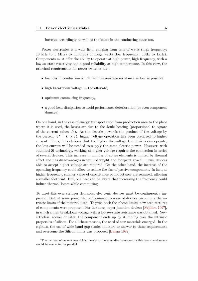
1.1. Power electronics stakes 5
increase accordingly as well as the losses in the conducting state too.
Power electronics is a wide field, ranging from tens of watts (high frequency:
10 kHz to 1 MHz) to hundreds of mega watts (low frequency: 10Hz to 1kHz).
Components must offer the ability to operate at high power, high frequency, with a
low on-state resistivity and a good reliability at high temperature. In this view, the
principal requirements for power switches are :
• low loss in conduction which requires on-state resistance as low as possible,
• high breakdown voltage in the off-state,
• optimum commuting frequency,
• a good heat dissipation to avoid performance deterioration (or even component
damage).
On one hand, in the case of energy transportation from production area to the place
where it is used, the losses are due to the Joule heating (proportional to square
of the current value: I2). As the electric power is the product of the voltage by
the current (P = U I), higher voltage operation has been preferred to higher
current. Thus, it is obvious that the higher the voltage the devices can operate,
the less current will be needed to supply the same electric power. However, with
standard Si technology, working at higher voltage requires the connection in series
of several devices. This increase in number of active elements is limited by thermal
effect and has disadvantages in term of weight and footprint space1. Thus, devices
able to accept higher voltage are required. On the other hand, the increase of the
operating frequency could allow to reduce the size of passive components. In fact, at
higher frequency, smaller value of capacitance or inductance are required, allowing
a smaller footprint. But, one needs to be aware that increasing the frequency could
induce thermal losses while commuting.
To meet this ever stringer demands, electronic devices must be continuously im-
proved. But, at some point, the performance increase of devices encounters the in-
trinsic limits of the material used. To push back the silicon limits, new architectures
of components were proposed. For instance, super-junction devices [Fujihira 1997],
in which a high breakdown voltage with a low on-state resistance was obtained. Nev-
ertheless, sooner or later, the component ends up by stumbling over the intrinsic
properties of silicon. For all these reasons, the need of new materials emerged. In the
eighties, the use of wide band gap semiconductors to answer to these requirements
and overcome the Silicon limits was proposed [Baliga 1982].
1The increase of current would lead nearly to the same disadvantages, in this case the elements
would be connected in parallel.
6 Chapter 1. Diamond for power electronics
1.1.2 Wide band gap semiconductors
Even if silicon remains dominant in power electronics, wide band gap materials such
as silicon carbide (SiC), gallium nitride (GaN) or even diamond constitute a serious
alternative. In fact, the large band gap of these semiconductors allows them to have a
higher breakdown field as well as the ability to operate properly at high temperature
due to a lower intrinsic carrier density. Indeed, if the off state of a device relies on
the insulation of an intrinsic layer of material, a too high intrinsic carrier density
would lead to a non negligible free carrier concentration when operating at high
temperature, and thus a leaky behavior in the off -state.
Gallium nitride
Gallium nitride (GaN), thanks to its direct band gap, emerged first in optoelec-
tronic and then in high frequency electronics. GaN bipolar transistor devices have
not yet emerged because of the difficulty to obtain p-type material. GaN is now
well recognized for high power and high frequency applications. Several devices
were reported in the last past ten years. An AlGaN/GaN Schottky diode showing a
breakdown voltage of 1kV was reported a few years ago [Yoshida 2006]. Ueda et al.
[H. Ueda 2005] demonstrated an HEMT (High Electron Mobility Transistor) that
can operate up to 300 C. GaN MOSFET with maximum mobility of 167 cm2/V.s
[Huang 2008] or 133 cm2/V.s at 250C [Nomura 2008] were also reported. More
complex lateral and vertical MOS structure with trench gate structure showing mo-
bility about 130 cm2/V.s can also be found in literature [Otake 2007, Otake 2008].
Contrary to SiC, GaN can be grown epitaxially onto silicon substrates which are
100 times cheaper than SiC ones. Besides, Fujitsu Semiconductor Limited company
recently announced the commercial availability of a silicon substrate-based gallium-
nitride power device that features a breakdown voltage of 150 V [Fujitsu 2013]. The
main asset of GaN technology is its reasonable cost as it can be heteroepitaxied on
Si substrate but it is only suitable for intermediate voltage (up to 600 V). Conse-
quently, technologies withstanding higher voltages are needed.
Silicon carbide
Silicon carbide (SiC) technology is more advanced when compared to GaN or
diamond. Indeed, SiC devices such as Schottky diodes, JFET and MOSFET with-
standing 1200 V voltage (and working up to 300C) are already commercialized
by Infineon (Europe), Rohm (Japan) or Cree (United States). Unfortunately, SiC
substrates are very expensive, 100 times more than silicon wafers. Nevertheless, a
lot of attention has been paid to this material by the power electronics community.
For instance, since february 2012, one on the six cars of the Ginza line subway
(Tokyo, Japan) has been equipped with a pair of SiC inverters from Mitsubishi
company [Mitsubishi 2013] which are 40 % smaller and lighter than the Si original
components. Moreover, according to the head of Mitsubishi’s transport systems
engineering section, a 38.6 % energy saving was recorded over one year of operation.

1.2. Diamond semiconductor 7
Such performances are promising but since power saving has become one of the
most significant and urgent societal and environmental needs, the use of "new"
materials offering the ultimate efficiency is now mandatory. A good candidate for
such breakthrough is diamond, which is considered as the ultimate semiconductor
offering better properties than SiC as it will be shown in the following.
1.2 Diamond semiconductor
Nowadays, silicon is ubiquitous in all branches of standard electronics. But wide
band gap semiconductors are preferred for power electronic applications such as
power converters, high power switches, rectifying diodes. The performances of the
most present innovative industrial technology which relies on discrete bipolar sil-
icon carbide transistor, should in theory be improved by using diamond. Indeed,
synthetic diamond single crystals represent an alternative route for unipolar power
devices (diodes, field-effect transistors).
1.2.1 Electrical properties
Diamond is a crystal made of carbon atoms arranged in a variation of face cen-
tered cubic crystal named diamond lattice. The wide band gap of diamond is the
direct consequence of the strong covalent bond of its atoms (strong elecronic inter-
action of the electrons close to the atomic nucleus due to the lightness of the carbon
atom). This large band gap ensures a high voltage withstand thanks to a high
breakdown electric field (10 MV/cm [Landstrass 1993, Volpe 2010]). The low mass
of the carbon atoms, which results in a high energy of lattice vibration (phonon),
allows an efficient transfer of heat. It has to be noticed that thermal conductivity
of diamond with a value of 22 W/cm.K is higher than most of the metals. Per-
not et al. [Pernot 2010] has shown that the high mobility at room temperature
µp=2000 cm2/V.s is a consequence of the low population of phonons (due to their
high energy).
In addition to physical properties (table 1.1), figures of merit (FoM) are gener-
ally used to compare semiconductors. The different FoM have to be used carefully
as each of them was developed for a certain field of applications. All the physical
properties used to calculate the following FoM are defined in table 1.1.
Johnson’s figure of merit (JFM): It represents the ability of a material for high
frequency and high power transistor applications [Johnson 1965]. This FoM is
both applicable for FET and with carefulness to bipolar transistor.
JFM =
FB.vs2
2
(1.1)
Keyes’ figure of merit (KFM): It displays the thermal limitation to the switch-

8 Chapter 1. Diamond for power electronics
Property [unit] Si 4H-SiC GaN Diamond
Band gap EG [eV] 1.1 i 3.23 i 3.45 d 5.45 i
Dielectric constant "r 11.8 9.8 9 5.5
Breakdown voltage FB [MV/cm] 0.3 3 2 10
Thermal conductivity λ [W/cm.K] 1.5 5 1.5 22
Sat. drift velocity e− vs [107 cm/s] 1.0 2.0 2.2 2.7
Sat. drift velocity h+ vs [107 cm/s] 1.0 1.1
Electrons mobility µe [cm2/V.s] 1500 1000 1250 1000
Holes mobility µh [cm2/V.s] 480 100 200 2000
Johnson’s FOM JFM [1023 Ω.W/s2] 2 911 490 3064
Keyes’ FOM KFM [107 W/K.s] 9 49 16 215
Baliga’s FOM BFM [Si=1] 1 554 188 23017
Table 1.1: Physical properties at room temperature of silicon (Si) and major wide
band gap materials (SiC, GaN, diamond) used in power electronics and the related
figures of merit (Johnson, Keyes and Baliga, see description in the text). In the band
gap row, i and d denote respectively an indirect and direct band gap. If temperature
dependent, the values are given at room temperature. The FoM were calculated at
300K for electrons except for diamond for which they are calculated for holes.
ing behaviour at high frequency [Keyes 1972].
KFM = λ
c.vs2."r
1/2
(1.2)
where c is the light velocity.
Baliga’s figure of merit (BFM): It defines material parameters to minimize
conduction losses in power applications [Baliga 1982, Baliga 1989].
BFM = "r.µ.F3B (1.3)
These three FoM were calculated and are reported for Si and for the major wide
band gap semiconductors SiC, GaN and Diamond in table 1.1. It should be noticed
that the figures of merit were calculated at 300 K for electrons, except for diamond
where holes were considered, as p-type diamond offers best properties and is used
in the present work. As shown on table 1.1, physical properties and FoM of dia-
mond overcome those of other usual semiconductors.The combination of all these
outstanding properties: a large band gap, high mobility, record breakdown field and
a very good thermal conductivity make of diamond the ultimate semiconductor for
high power and high frequency devices [Ohashi 2012] as represented on the roadmap
of figure 1.2.
Systems such as power converters and switches are made of silicon or silicon carbide
at the moment. Thanks to the superior properties of diamond, the size of such

1.2. Diamond semiconductor 9
devices could be dramatically reduced while the performances would be improved.
For instance, thanks to the weight gain (less elements, reduced cooling system) and
efficiency improvement, the use of diamond in public transport sector would allow
to reduce the losses by a factor of three with respect to the use of Si. In France,
ALSTOM company2 is interested by diamond power devices to replace Si IGBT
pack in the trains. Similarly, Umezawa et al. [Umezawa 2012] predicted a 90% of
reduction losses by using diamond Schottky diodes instead of SiC devices for high
temperature power applications.
Figure 1.2: Roadmap of the
future advance power devices
from [Ohashi 2012] showing
the predicted evolution in
semiconductor use.
1.2.2 Diamond materials
One of the major issue limiting the development of diamond electronics is the sub-
strate size for single crystal diamond homo-epitaxy. Moreover, diamond substrates
are expensive and the quality varies widely.
Most of the diamond substrates are fabricated at high pressure and high tempera-
ture (HPHT) technique mimicking the natural formation condition. There are two
types of HPHT substrates : i) Ib which contains a lot of isolated substitutional ni-
trogen atoms (few 1019 cm−3) and ii) IIa which are grown using a technique making
them purer. Both of them are insulating at room temperature as the nitrogen is a
deep level in the gap at 1.7 eV from the conduction band. Typical sizes available for
HPHT substrate depend on their crystalline orientation : 33 mm2 for [100] oriented
crystal and 22 mm2 for [111] oriented crystal. The two main suppliers of HPHT
substrates are Sumitomo from Japan and Element 6 from United Kingdom. Chem-
ical vapor deposition is also used for growing diamond substrates. Thanks to recent
progress, significantly larger substrate sizes, and up to 88 mm2 plates haves be-
come commercially available. Diamond substrate growth is constantly progressing,
in particular because diamond has been recognized as the ultimate semiconductor
for power electronics.
2In the framework of Diamonix 2 project.

10 Chapter 1. Diamond for power electronics
Layers investigated in this work were mainly grown on Ib [100] and IIa [100] HPHT
diamond substrates.
1.2.3 Doping of diamond
Figure 1.3: Schematics of the diamond
band diagram with the main n-type and
p-type known dopants. EG =
5.5
eV
Conduction band
Energy
Phosphorous
Nitrogen
Boron
0.38 eV
1.7 eV
0.57 eV
Valence band
For a long time, diamond had been considered as an insulator due to its wide
band gap energy (5.45 eV) and to the impossibility to dope it. Boron doping and
then phosphorous doping by incorporation during the growth by microwave plasma
enhanced chemical vapor deposition (MPCVD) have been discovered respectively
twenty and sixteen years ago. These discovers allow to have p-type and n-type
semiconducting diamond, opening the route for diamond based electronic devices.
1.2.3.1 n-type doping
Nitrogen (N) is known to be a n-type dopant, found in natural diamond. But as its
activation energy is very high: 1.7 eV (see Fig. 1.3), no electronic devices can be
based on using N as a dopant. Nevertheless, nitrogen doped diamond is intensively
studied for quantum optics and spintronics applications using nitrogen vacancy (NV)
complexes.
Shallower possible n-type dopants were investigated and the shallowest known to-
day is phosphorous (P) with a donor level lying in the gap at 570 meV from the
conduction band. The first convincing demonstration of phosphorous doping was
reported on [111] orientated diamond by Koizumi et al. [Koizumi 2001]. More re-
cently Kato et al. [Kato 2005] demonstrated the phosphorous doping during [100]
growth despite the fact that phosphorous is known to not incorporate well for this
orientation. At the moment, phosphorous is the only usable known n-type dopant
1.2. Diamond semiconductor 11
but unfortunately its elevated ionization energy results in a very low carrier concen-
tration at room temperature : n/[P] = 1/106 meaning that one P dopant atom
in a million is ionized.
1.2.3.2 p-type doping
Incorporation of boron atoms during the MPCVD growth process leads to an accep-
tor level at 380 meV above the valence band. This level has been well studied during
the last past sixteen years by electrical measurements [Werner 1997, Thonke 2003,
Tsukioka 2006, Mortet 2008, Gabrysch 2008, Volpe 2009]. One of the most interest-
ing properties of boron doped diamond is the gradual evolution from a semiconductor
to a metal when increasing the boron doping level above 51020 cm−3. The ionisa-
tion energy of boron is 380 meV at low doping levels and tends toward zero as the
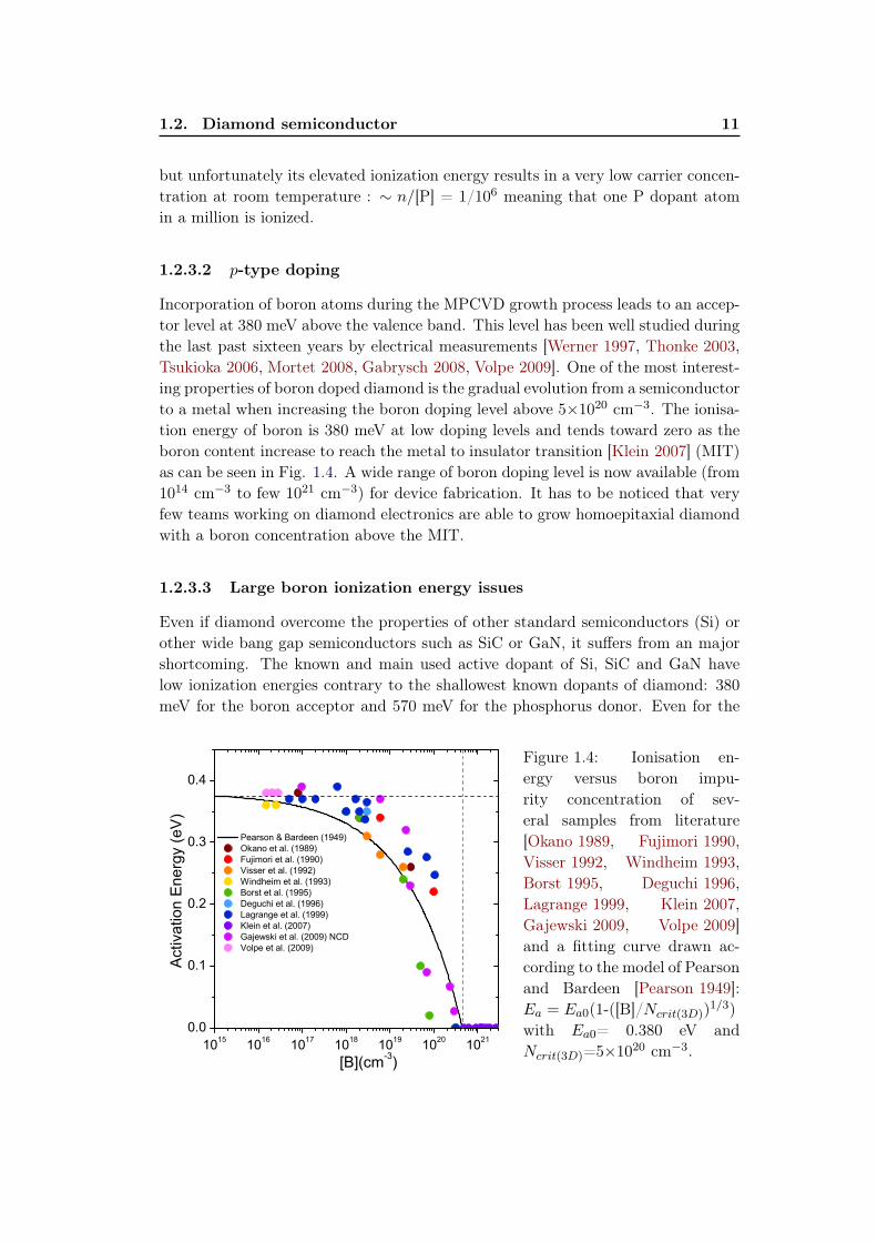
boron content increase to reach the metal to insulator transition [Klein 2007] (MIT)
as can be seen in Fig. 1.4. A wide range of boron doping level is now available (from
1014 cm−3 to few 1021 cm−3) for device fabrication. It has to be noticed that very
few teams working on diamond electronics are able to grow homoepitaxial diamond
with a boron concentration above the MIT.
1.2.3.3 Large boron ionization energy issues
Even if diamond overcome the properties of other standard semiconductors (Si) or
other wide bang gap semiconductors such as SiC or GaN, it suffers from an major
shortcoming. The known and main used active dopant of Si, SiC and GaN have
low ionization energies contrary to the shallowest known dopants of diamond: 380
meV for the boron acceptor and 570 meV for the phosphorus donor. Even for the
1015
1016
1017
1018
1019
1020
1021
0.0
0.1
0.2
0.3
0.4
Pearson & Bardeen (1949)
Okano et al. (1989)
Fujimori et al. (1990)
Visser et al. (1992)
Windheim et al. (1993)
Borst et al. (1995)
Deguchi et al. (1996)
Lagrange et al. (1999)
Klein et al. (2007)
Gajewski et al. (2009) NCD
Volpe et al. (2009)
Activa
tio
n E
ne
rgy (
eV
)
[B](cm-3)
Figure 1.4: Ionisation en-
ergy versus boron impu-
rity concentration of sev-
eral samples from literature
[Okano 1989, Fujimori 1990,
Visser 1992, Windheim 1993,
Borst 1995, Deguchi 1996,
Lagrange 1999, Klein 2007,
Gajewski 2009, Volpe 2009]
and a fitting curve drawn ac-
cording to the model of Pearson
and Bardeen [Pearson 1949]:
Ea = Ea0(1-([B]/Ncrit(3D))1/3)
with Ea0= 0.380 eV and
Ncrit(3D)=51020 cm−3.
12 Chapter 1. Diamond for power electronics
boron p-type dopant [Lagrange 1998, Volpe 2009] which is lower than phosphorous,
this high ionization results in a equilibrium carrier concentration p very low at room
temperature (about 1 in 103 boron acceptor is ionized, p/[B]=1/103 for low doped
diamond) and thus a very high on state resistivity ( 100 Ω/cm for boron doped di-
amond at [B]=1016 cm−3 with no compensation). As a consequence, diamond seems
ill-suited to some devices such as metal semiconductor field effect transistors (MES-
FET), bipolar junction transistors (BJT) or junction field effect transistors (JFET)
where the on-state conductivity is directly linked to that of the active layer.
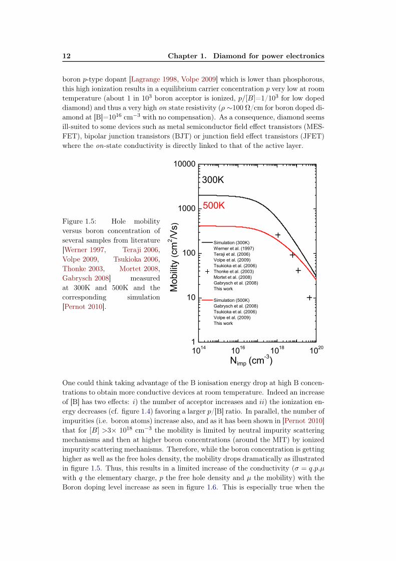
Figure 1.5: Hole mobility
versus boron concentration of
several samples from literature
[Werner 1997, Teraji 2006,
Volpe 2009, Tsukioka 2006,
Thonke 2003, Mortet 2008,
Gabrysch 2008] measured
at 300K and 500K and the
corresponding simulation
[Pernot 2010].
1014
1016
1018
1020
1
10
100
1000
10000
Simulation (300K)
Werner et al. (1997)
Teraji et al. (2006)
Volpe et al. (2009)
Tsukioka et al. (2006)
Thonke et al. (2003)
Mortet et al. (2008)
Gabrysch et al. (2008)
This work
Simulation (500K)
Gabrysch et al. (2008)
Tsukioka et al. (2006)
Volpe et al. (2009)
This work
500K
Mobili
ty (
cm
2/V
s)
Nimp
(cm-3)
300K
imp
One could think taking advantage of the B ionisation energy drop at high B concen-
trations to obtain more conductive devices at room temperature. Indeed an increase
of [B] has two effects: i) the number of acceptor increases and ii) the ionization en-
ergy decreases (cf. figure 1.4) favoring a larger p/[B] ratio. In parallel, the number of
impurities (i.e. boron atoms) increase also, and as it has been shown in [Pernot 2010]
that for [B] >3 1018 cm−3 the mobility is limited by neutral impurity scattering
mechanisms and then at higher boron concentrations (around the MIT) by ionized
impurity scattering mechanisms. Therefore, while the boron concentration is getting
higher as well as the free holes density, the mobility drops dramatically as illustrated
in figure 1.5. Thus, this results in a limited increase of the conductivity (σ = q.p.µ
with q the elementary charge, p the free hole density and µ the mobility) with the
Boron doping level increase as seen in figure 1.6. This is especially true when the

1.3. State of the art of diamond devices 13
1015
1016
1017
1018
1019
1020
10-3
10-2
10-1
100
101
ND= 0
ND= [B]/100
ND= [B]/10
σ (
S/c
m)
[B] (cm-3)
T = 300KFigure 1.6:
Simulated
conductivity
of diamond
versus boron
concentration
at 300 K
for different
compensation
density.
compensation density become non negligible. For instance, for a 10% compensated
diamond (black line on Fig. 1.6) the conductivity increase occurs at a doping level
for which the mobility is already quite low. Thus it seems impossible to combine
the high conductivity and the high mobility with simple devices.
1.3 State of the art of diamond devices
The need for efficient and low loss high power and high frequency devices is real
and urgent. We have seen that even if SiC substrates are more expensive than
silicon (100 times), SiC based devices are welcome in the high power sector and
start to be used in public transportation (Ginza line, Tokyo, Japan). Then, we
can fully understand that the shortcomings of diamond could be compensated by
its superlative properties. That is why several research laboratories (sometimes in
collaboration with industrial partners) are working actively on diamond to propose
solutions to get rid of these weaknesses. The important progress that has been made
recently in the field of substrate fabrication, epi-layer growth and doping control
should in principle allow to develop new low loss electric switches [Balmer 2008].
Since both n-type and p-type doping of diamond are mastered, several conceptual
and working devices have been reported in literature.
1.3.1 Bipolar devices
Thanks to the mastering of n-type doping, Koizumi et al. reported an ultraviolet
light-emitting diode based on a diamond pn junction [Koizumi 2001]. A pn junction
was also reported by Tavares et al. in 2005 [Tavares 2005]. In 2006, a Schottky-pn
diode, which is claimed to overcome weak points of Schottky diodes and pn junc-
tion and showing a good rectification ratio was proposed [Makino 2009]. AIST
also reported an emitting pin junction where the emission spectra was improved
compared to classical pn junction [Makino 2008]. Progress allowing to selectively
grow n-type diamond on the [111] direction on a [001] substrate allowed to consider
14 Chapter 1. Diamond for power electronics
lateral pn junction [Kato 2009]. Recent papers reported fabrication of bipolar tran-
sistors using this technique [Kato 2013]. All these demonstrations are promising
and diamond bipolar technology is an efficient way to perform high voltage device.
However, at the moment, these devices suffer from the high ionisation energy of
n-type diamond. Recently it has been proposed to solve this issue by taking benefit
of the low resistance of hopping conduction (which dominates in highly phospho-
rous doped diamond for [P] > 1019 cm−3 [Sato 2000, Kato 2008]) in pin junction
[Oyama 2009, Oyama 2011].
1.3.2 Unipolar devices
In power electronics, the field effect transistor and the Schottky diode are two com-
plementary switches for the commutation cell in converter of power electronics.
Recently, in the framework of a collaboration between Institut Néel, Ampère, ISL
and NIMS (Japan), a 10kV diamond Schottky diode was reported [Volpe 2010]. In
D G S
p-
i
MESFET C-H bonded FET
D G S
p-(H )
i
MOSFET
D G S
n inversionchanneli
p-
D G S
δ-layer
i
δ-FET(d)
(b)(a)
(c)
n+ n+
Oxide
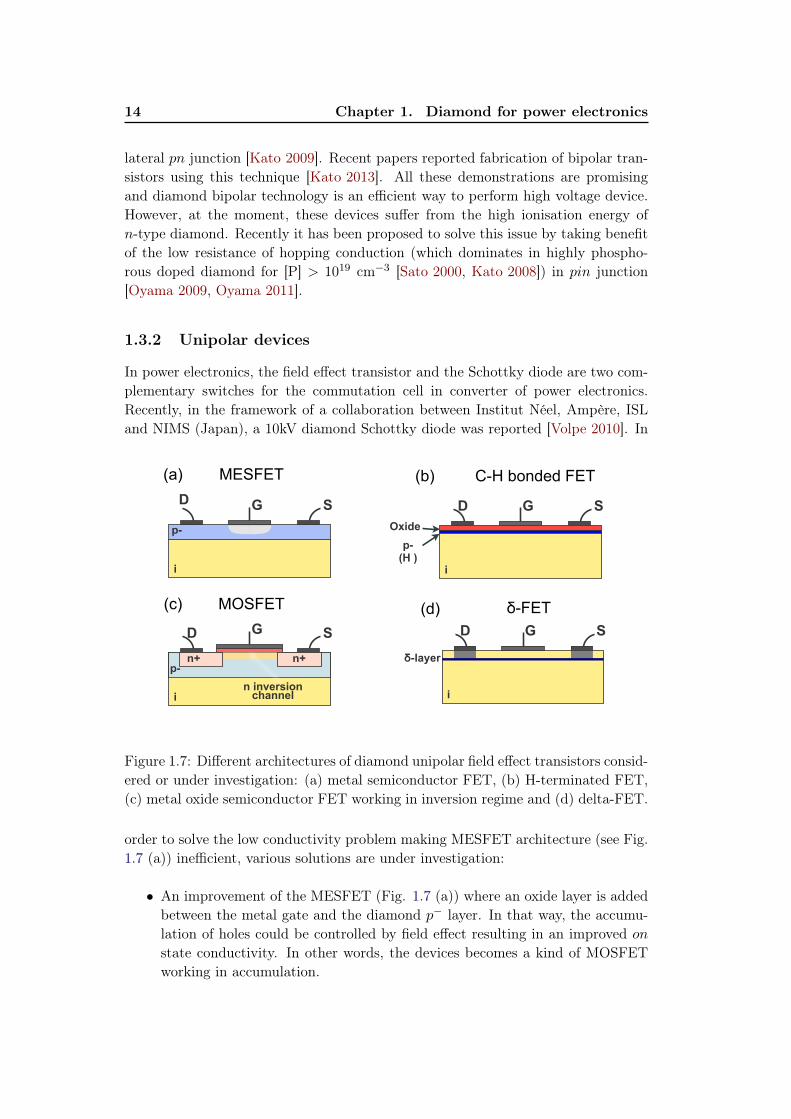
Figure 1.7: Different architectures of diamond unipolar field effect transistors consid-
ered or under investigation: (a) metal semiconductor FET, (b) H-terminated FET,
(c) metal oxide semiconductor FET working in inversion regime and (d) delta-FET.
order to solve the low conductivity problem making MESFET architecture (see Fig.
1.7 (a)) inefficient, various solutions are under investigation:
• An improvement of the MESFET (Fig. 1.7 (a)) where an oxide layer is added
between the metal gate and the diamond p− layer. In that way, the accumu-
lation of holes could be controlled by field effect resulting in an improved on
state conductivity. In other words, the devices becomes a kind of MOSFET
working in accumulation.

1.3. State of the art of diamond devices 15
• A famous architecture for high frequency diamond devices is the Hydrogen-
terminated diamond FET (Fig.1.7) (b)) using a 2D hole gas at the surface.
Several demonstrators were reported in the literature [Kasu 2006, Hirama 2006,
Hirama 2010, Kasu 2012]. Such transistors demonstrate high frequency opera-
tion (up to 45 GHz) but in most of the case deteriorate under high temperature
conditions. Recently, the use of an oxide to stabilize the hydrogenated surface
was reported to get rid of this problem [Hiraiwa 2012]. This is a promising
architecture for high frequency transistor but not for high voltage devices.
• In 2011, Imura et al. reported the first AlN/diamond heterojunction field
effect transistor. It was shown that this heterojunction FET acts as a p-
channel FET with a normally-on depletion mode. The holes are accumulated
in the diamond near the nitride/diamond interface [Imura 2011]. Even if the
electrical transport mechanism is not yet well understood, this architecture is
promising for high frequency transistors.
• Boron δ-FET (Fig.1.7 (d)), which consists of a thin heavily doped (metallic)
layer between two intrinsic layers resulting theoretically in high mobility, has
been intensively studied by several groups : Institut Néel (France), E6, UCL
(united Kingdom), Waseda University (Japan) and Ulm university (Germany).
Thus several studies of delta structures were reported recently [Elhajj 2008,
Tumilty 2009, Chicot 2012, Edgington 2012, Scharpf 2013, Balmer 2013].
• Another concept to overcome this issue relies on the electron inversion channel
used in the ubiquitous MOSFET. The inversion regimes require a sufficiently
clean oxide/SC interface to avoid the pinning of the Fermi level. Up to now,
among the several MOS structures reported in literature [Kawakami 2005,
Hirama 2006, Hirama 2010, Kasu 2012, Cheng 2012] none of them exhibited
deep depletion or inversion regime.
This PhD work is focused on the latter two proposed solutions, which may ad-
dress different sectors of power electronics.
The delta-FET is aimed at high frequencies. One can expect good performances
at high frequency if the numerous carriers from the delta layer could effectively flow
in a high mobility region (non intentionally doped to maximize the mobility). Thus
this architecture is in direct competition with the H-terminated FET. Such a tran-
sistor would be normally on without applied bias. High frequency diamond delta
FET would have a consequent advantage over GaN HEMT : the ability to evacuate
efficiently the heat when commuting at high frequencies. So, the challenge is to
achieve a mobility as high as the state of the art of GaN HEMT : 2200 cm2/V.s
which allows operating frequency up to 300 GHz [Chung 2010].
The diamond MOSFET, could be considered than for intermediate frequency ap-
plications (lateral MOSFET) as well as high power application with an adapted
16 Chapter 1. Diamond for power electronics
vertical architecture3. Its main advantages over bipolar transistor would be its high
commutation speeds (no need to remove minority carriers). The inversion MOSFET
would be normally off (if the work function of the oxide is well chosen with respect
to that of the SC). This is a non negligible advantage for energy saving in high
power electronics. At the moment Si MOSFET are widely used in low voltage (<
200V) switches. However, MOSFET have also been used in high voltage switches
ever since SiC MOSFET withstanding 1200 V voltage are commercially available
(from CREE company). If achieved in diamond one can expect to have MOSFET
withstanding higher voltage (thanks to a higher breakdown field) with a better com-
muting speed (thanks to higher mobility) and with an improved heat dissipation,
which would avoid the channel degradation in harsh environment which is known
to occurs in SiC MOSFET.
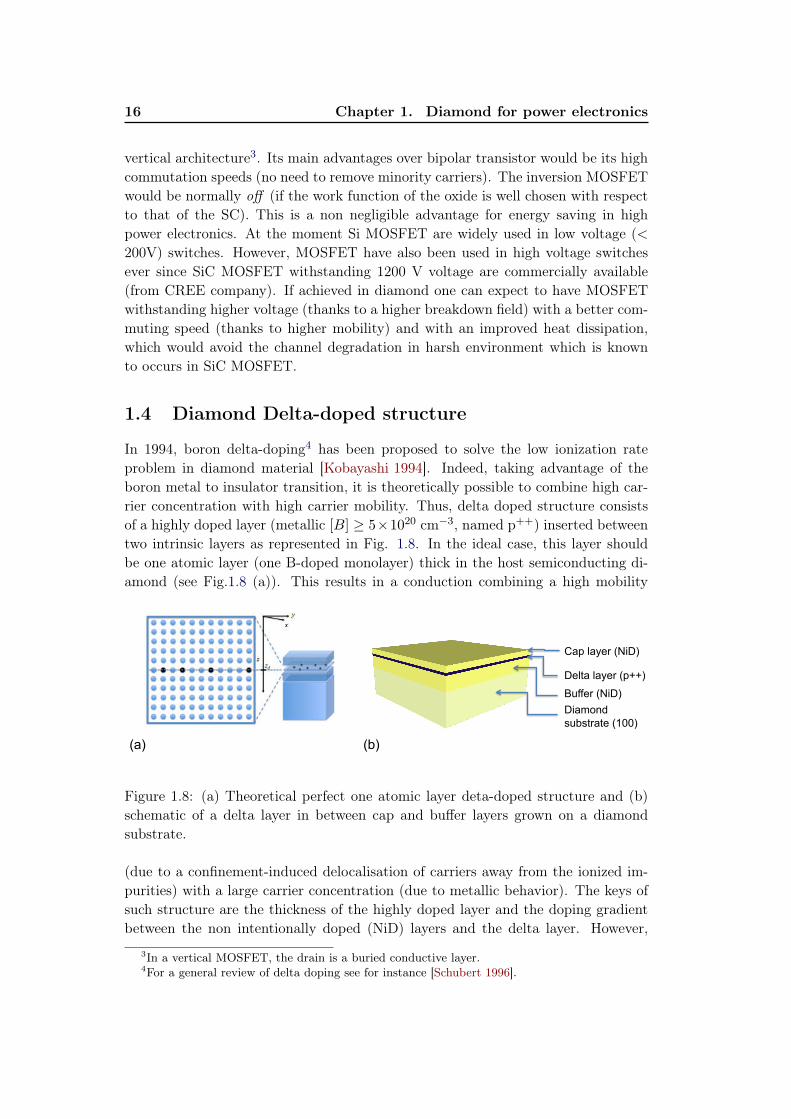
1.4 Diamond Delta-doped structure
In 1994, boron delta-doping4 has been proposed to solve the low ionization rate
problem in diamond material [Kobayashi 1994]. Indeed, taking advantage of the
boron metal to insulator transition, it is theoretically possible to combine high car-
rier concentration with high carrier mobility. Thus, delta doped structure consists
of a highly doped layer (metallic [B] ≥ 51020 cm−3, named p++) inserted between
two intrinsic layers as represented in Fig. 1.8. In the ideal case, this layer should
be one atomic layer (one B-doped monolayer) thick in the host semiconducting di-
amond (see Fig.1.8 (a)). This results in a conduction combining a high mobility
Diamond
substrate (100)
Buffer (NiD)
Cap layer (NiD)
Delta layer (p++)
(a) (b)
Figure 1.8: (a) Theoretical perfect one atomic layer deta-doped structure and (b)
schematic of a delta layer in between cap and buffer layers grown on a diamond
substrate.
(due to a confinement-induced delocalisation of carriers away from the ionized im-
purities) with a large carrier concentration (due to metallic behavior). The keys of
such structure are the thickness of the highly doped layer and the doping gradient
between the non intentionally doped (NiD) layers and the delta layer. However,
3In a vertical MOSFET, the drain is a buried conductive layer.4For a general review of delta doping see for instance [Schubert 1996].

1.5. Metal Oxide Semiconductor with diamond 17
some limitations need to be overcome to obtain these two properties. Obviously,
growing thin layers is a technological challenge and implies a very accurate control of
thickness during the growth. But even assuming this challenge was met, the initial
roughness of the substrate will be a source of shortcomings. Indeed, the delta-layer
should very thin to obtain a quantum confinement and delocalisation of carrier.
Traget thickness (nano-metric scale) is in the same order than the roughness of the
best polished substrate. Another limitation, will be the doping level control: the
delta layer doping level must be above the MIT and cap (and also buffer) layer dop-
ing level must be as low as possible. Depending of the strategy used to grow such
stack, growth reactor chamber memory effect could be an obstacle to obtain a suf-
ficiently large gradient without broadening too much the interface between metallic
part (delta-layer) and insulating part (cap and buffer layers). However, diamond
offers an advantage and not the least compared to standard semiconductors such as
Si and GaAs where delta-doping has been investigated and is now exploited : boron
atoms do not diffuse in diamond. In the case of delta-doping based devices, this
would be a stability guarantee. Indeed, whether it be during the fabrication process
(growth at around 900C and annealing of ohmic contact at 750C) or during the
final device operation, the delta structure will be exposed to very high temperature.
Several issues need to be overcome before being able to fabricate an efficient delta-
FET. Therefore in the next chapters, this manuscript will answer to the following
questions :
• Can delta-structure with a nano-metric sized delta layers and with a suffi-
ciently large doping gradient between NiD and p++ layer be grown ? (chapter 2)
• If nano-metric sized layer achieved, will this delta layer show an improve-
ment of mobility over bulk diamond to be competitive with present HEMT ?
(chapter 3)
1.5 Metal Oxide Semiconductor with diamond
The metal oxide semiconductor (MOS) structure is a specific case of metal insulator
semiconductor (MIS) structure where the insulator is an oxide. As indicated by its
name, it is a stack of a semiconductor, oxide and metal as represented on figure 1.9
in its simplest form.
p"semiconductor.
Metal
Oxide
Ohmic
contact
V
dox
Figure 1.9: Metal-oxide-
semiconductor (MOS) capaci-
tor, in its simplest form.
18 Chapter 1. Diamond for power electronics
In this work we aim at a diamond MOSFET. In this context, the study of the MOS
capacitor is a prerequisite. MIS structures have been used as voltage-controlled
varistors (variable capacitors) since 1959. The first successful MIS structure made
of SiO2 on Si led immediately to the report of the famous Si MOSFET which is now
ubiquitous in analog and digital electronics. Thanks to sufficiently clean SiO2/Si
interface, the inversion regime can be reached in silicon. On the contrary, in the
case of most semiconductors this regime has never been reached.
The conducting or insulating behavior of the MOSFET is based on the electrostatic
control of the band curvature at the oxide/semiconductor interface. Unfortunately,
the physical properties of Si semiconductor do not allow to build efficient MOSFET
for power electronics application (generally insulated gate bipolar transistor are pre-
ferred but also limited to 4 kV). MOSFET based on other semiconductors, like III-V
compounds or SiC, are improving but the performances of such devices are not com-
petitive with Si devices and anyway, will be always lower than those expected for a
diamond based MOSFET. The electrostatic control of the band curvature is a pos-
sible solution to solve the issue of the low ionization rate of the diamond dopants,
but requires clean and low defect interfaces between oxide and semiconductor, to
avoid the Fermi level pinning at the interface. Therefore, MOS structures mades of
diamond as a semiconductor must be studied first, before fabricating MOSFET, in
order to answer questions such as:
• Can a diamond MOS structure allowing an electrostatic control of the channel
be achieved ? (chapter 4)
• If achieved, will the interface oxide/diamond be sufficiently clean to avoid the
Fermi level pinning and allow to reach the inversion layer in a MOSFET ?
(chapter 4)
Chapter 2
Growth and characterization
techniques
Contents
2.1 Epilayer growth and characterization . . . . . . . . . . . . . 20
2.1.1 Key points for delta growth . . . . . . . . . . . . . . . . . . . 20
2.1.2 MPCVD technique and reactor . . . . . . . . . . . . . . . . . 20
2.1.3 Epilayer characterization . . . . . . . . . . . . . . . . . . . . 22
2.1.4 Doping level control . . . . . . . . . . . . . . . . . . . . . . . 24
2.1.5 Thickness and interface control . . . . . . . . . . . . . . . . . 26
2.1.6 Nanometric delta-layers growth . . . . . . . . . . . . . . . . . 28
2.1.7 Diamond epilayer for MOS structure . . . . . . . . . . . . . . 31
2.2 Hall effect and four probe measurements . . . . . . . . . . . 32
2.2.1 Hall effect principle . . . . . . . . . . . . . . . . . . . . . . . 32
2.2.2 Sheet carrier density measurements . . . . . . . . . . . . . . . 34
2.2.3 Resistivity and mobility measurements . . . . . . . . . . . . . 35
2.2.4 Mesa structured Hall bar . . . . . . . . . . . . . . . . . . . . 36
2.2.5 Experimental set-up . . . . . . . . . . . . . . . . . . . . . . . 40
2.2.6 Reproducibility of measurements . . . . . . . . . . . . . . . . 40
2.3 Conclusion . . . . . . . . . . . . . . . . . . . . . . . . . . . . . 41
The main topic of this PhD project is the electrical characterization of delta-
doped and MOS structures. However, I undertook all the fabrication steps of the
samples and the devices I characterized, from substrates surface preparation to
nano-fabrication process (etching, patterning, mask designing, lithography) includ-
ing diamond epilayer growth.
In a first section the homo-epitaxial diamond growth techniques adapted to delta
layer growth will be described. Studies led to reach nanometric size layer as well
as the physical characterization technique use to validate growth result will be pre-
sented. In a second section four probe resistivity and Hall effect measurements
principles will be detailed, as well as some experimental aspects such as Hall bar
fabrication.

20 Chapter 2. Growth and characterization techniques
2.1 Epilayer growth and characterization
A pioneering study of the growth of delta structures, which had required growth
reactor modifications, has been done by Alexandre Fiori during his PhD thesis
[Fiori 2012a]. During one year and half, I worked and collaborated with him to
learn growth and especially aspects related to thin and heavily doped layers and
to continue the investigation on delta-layer growth improvements. As a major part
of this growth work is well detailed in A. Fiori’s PhD manuscript, I shall restrict
myself here to studies to which I contributed and points related to the samples that
I characterized in this work.
First, I shall recall the key points in growing a delta layer, then present some studies
related to delta layer obtention, and finally provide the growth and process details
specific to the samples characterized during this PhD work. It has to be noticed
that this section is principally focused on delta growth as it is technically speaking
more demanding. However, growth techniques used for diamond epilayers of MOS
structures are the same and some recipes are common or very similar between delta
and MOS.
2.1.1 Key points for delta growth
Delta structures growth is very refined and technical. The first obvious issue concern
the thickness of the layer which needs to be very low and accurately controlled. To
do that, slow growth rates are preferred. The growth must also keep (or improve)
the initial roughness of the sample by avoiding as much as possible growth defects
appearance. The second point is the doping level of each layer. On one hand, as
a high mobility is required in the cap and buffer layers, the boron concentration
needs to be there as low as possible. Oxygen is added in the gas phase to reduce
boron contamination as described by Volpe et al. [Volpe 2009]. On other hand,
high boron concentration is required in the delta layers in order to reach the MIT.
In order to avoid growth interruption and the defects due to growth re-start, it
has been chosen to grow all the delta structure without interrupting the plasma.
Therefore, close attention must be paid to the interface between low and highly
doped materials which have to be as abrupt and clean as possible. Indeed, a top
hat shape with infinite slope would be the perfect doping profile. In addition, the
transition part should be defect free otherwise the conductivity could be lowered
in this region supposed to host the delocalized carrier. Uniformity of the layer is
also important to obtain homogeneous layer in term of doping level and thickness
all over the diamond sample surface. In this way, all the diamond sample surface
would be available for devices fabrication.
2.1.2 MPCVD technique and reactor
Samples for this work were grown by microwave plasma-enhanced chemical vapor
deposition in a vertical silica tube NIRIM-type reactor which is so called after the
2.1. Epilayer growth and characterization 21
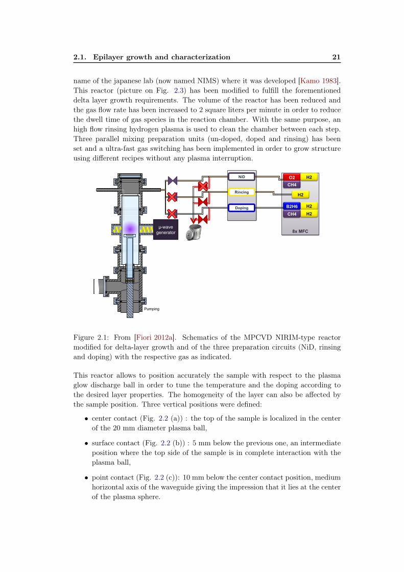
name of the japanese lab (now named NIMS) where it was developed [Kamo 1983].
This reactor (picture on Fig. 2.3) has been modified to fulfill the forementioned
delta layer growth requirements. The volume of the reactor has been reduced and
the gas flow rate has been increased to 2 square liters per minute in order to reduce
the dwell time of gas species in the reaction chamber. With the same purpose, an
high flow rinsing hydrogen plasma is used to clean the chamber between each step.
Three parallel mixing preparation units (un-doped, doped and rinsing) has been
set and a ultra-fast gas switching has been implemented in order to grow structure
using different recipes without any plasma interruption.
8x MFC µ-wave
generator
NiD
Rincing
Doping
H2
H2
H2
O2
CH4
B2H6
CH4
Pumping
H2
Figure 2.1: From [Fiori 2012a]. Schematics of the MPCVD NIRIM-type reactor
modified for delta-layer growth and of the three preparation circuits (NiD, rinsing
and doping) with the respective gas as indicated.
This reactor allows to position accurately the sample with respect to the plasma
glow discharge ball in order to tune the temperature and the doping according to
the desired layer properties. The homogeneity of the layer can also be affected by
the sample position. Three vertical positions were defined:
• center contact (Fig. 2.2 (a)) : the top of the sample is localized in the center
of the 20 mm diameter plasma ball,
• surface contact (Fig. 2.2 (b)) : 5 mm below the previous one, an intermediate
position where the top side of the sample is in complete interaction with the
plasma ball,
• point contact (Fig. 2.2 (c)): 10 mm below the center contact position, medium
horizontal axis of the waveguide giving the impression that it lies at the center
of the plasma sphere.

22 Chapter 2. Growth and characterization techniques
(a) (b) (c)
5 mm
5 mm
Sample Plasma
Tube
wa
ve
gu
ide
lower wall
medium
axis
upper wall
Figure 2.2: (a) center contact, (b) surface contact and (c) point contact positions
of the samples in regards to the plasma ball. From [Fiori 2012a]
Schematics of the reactor with the sample positioning system, the microwave gen-
erator and the 3 independent mixture preparations units can be seen on figure 2.1
as well as on the pictures of figure 2.3.
Figure 2.3: Pictures of (a) the whole MPCVD set-up with reaction and loading
chamber on the left side and control panel on the right side and (b) the reaction
chamber and microwave guide.
2.1.3 Epilayer characterization
Once the sample was grown, it could be characterized by different methods. In this
work, the main methods were secondary ion mass spectroscopy (SIMS) performed
2.1. Epilayer growth and characterization 23
in GEMaC (France) by François Jomard, transmission electron microscopy (TEM)
performed in Cadiz university UCA (Spain) by Daniel Araujo et al. and ellipsometry
performed in Institut Néel (France) by David Eon et al.. Feedback and cross checking
of such data allow us to calibrate our process from the growth rate to the doping
level. In addition, different surface characterization methods were also used to
compare the sample surface before and after growth, with a particular focus on the
roughness.
2.1.3.1 Secondary Ion Mass Spectrometry
Principle
Secondary ion mass spectrometry (SIMS) is a technique allowing to analyze the
chemical composition of thin films as a function of depth. The specimen surface
is sputtered with a focused primary ion beam and the ejected secondary ions are
collected and analyzed with a mass spectrometer. Thus it is possible to detect
different elements with concentrations as low as 1015 cm−3 to 1016 cm−3 in diamond
depending on the elements. The secondary ion signal is given as a function of the
sputtering time but can be converted in depth when the end depth of the crater is
measured. SIMS is a destructive characterization as material are removed leaving
a crater of several hundreds of micrometer square. One should note that SIMS
analysis gives the total density of an impurity, but not the electrically active one.
Experimental set-up
SIMS measurements shown in this work were performed using O+2 as primary ions
at 1 keV and Cs+ at 15 keV in a Cameca IMS 4f or 7f set-up, and collecting the
negative secondary ions 11B.
2.1.3.2 Transmission Electron Microscopy
Principle
Transmission electron microscopy (TEM) is a microscopy technique in which an
electron beam is transmitted through an ultra-thin specimen. The interactions of
electrons when passing through the specimen give rise to an image. This image must
be magnified and focused on an imaging medium (fluorescent screen, photographic
film or CCD sensor for instance) to be used and interpreted. TEM has a very good
resolution (best around 0.2 nm) which is about 1000 times better than ordinary
light microscope. Thank to this, the examination of very small details in principle
down to the single atomic column level in cross section (i.e. single atom thickness).
Such analysis must be performed on sufficiently thin specimen sample in order to
be electron transparent. In the case of diamond, which is known to be the hardest
material, the sample preparation to obtain thin lamella (few tens of nanometers) is
a complex procedure involving FIB (Focus Ion Beam). Consequently, this charac-
terization technique is destructive.

24 Chapter 2. Growth and characterization techniques
Experimental set-up
High-angle annular dark-field imaging (HAADF) images were taken in the scan-
ning mode in a Jeol 2010 TEM with a 200 kV beam, 0.7 nm probe size and a 8 cm
camera length. Samples were prepared thanks to a Quanta 200 3D FIB, with a final
thickness of approximately 70 nm as detailed elsewhere in Ref. [Araùjo 2013].
2.1.3.3 Ellipsometry
Principle
Ellipsometry is an optical technique providing access to the dielectric properties
of thin films. In some cases, it can be also used to characterize the composition,
the roughness, the thickness and the electrical conductivity of materials. Techni-
cally speaking, ellipsometry measures a change in polarization as light reflects from
or transmits through a material structure. This polarization ratio at interfaces is
represented as an amplitude ratio and the phase difference. In the case of a flat mul-
tilayer, the measured response depends on optical properties and thickness of each
material constituting the analyzed specimen. Thus, this technique is a powerful and
non destructive tool to determine the thickness of layers without contact. Moreover,
it is possible to perform in-situ ellipsometry measurement during the growth of a
sample. For all these reason, ellipsometry appears to be a powerful tool to charac-
terize delta structures by taking advantages of of the difference in refractive index
between NiD and p++ diamond [Bousquet 2014].
Experimental set-up
Spectroscopic Ellipsometry measurements were performed from 250 to 1000 nm
in air using a Woollam M-2000 ellipsometer. The experimental spectra have been
fitted to numerical simulations as described elsewhere in Ref. [Bousquet 2014].
2.1.4 Doping level control
2.1.4.1 Non intentionally doped diamond
Cap layer and buffer layer must be as low doped as possible in order to provide a
high mobility region to delocalized holes. But, even without adding boron in the
gas phase during the growth, the layer still contains boron atoms which can come
from contamination of the reactor. Such layers are called non intentionally doped
(NiD) because of this possible residual doping. It has been shown that adding
oxygen in the gas phase allows to reduce the boron contamination [Volpe 2009].
Therefore a standard NiD recipe was created : a 50 Torr CH4/O2/H2 mixture (1%,
0.25%, 0.9875 molar) flowing at 200 sccm. Later this recipe has been modified
as follows CH4/O2/H2 (0.75%, 0.32%, 0.9893 molar) to favor lateral growth (i.e.
vertical growth rate lower than lateral growth rate) in order to reduce the surface
roughness (polishing lines, craters). This is particularly crucial before growing thin
delta-layers. Both sets of mixtures have been used to grow samples studied in this
work.

2.1. Epilayer growth and characterization 25
2.1.4.2 Heavily doped layer
As previously described in section 1.4, the doping level of the delta layer has to be
above the critical concentration Ncrit(3D) of the MIT to obtains carrier density equal
to the doping level. In fact, at a given temperature, the smaller the activation energy
(it decreases with the doping level), the higher the carrier density. A full activation
of the boron acceptors is ensured for a doping level above Ncrit(3D) (i.e. [B] > 5 1020 cm−3). In addition, in order to control accurately the thickness, a slow growth
condition will be preferred. Diborane B2H6 is used as the boron source in this work
but other gas, such as trimethylboron (TMB) can also be used[Volpe 2012b].
The main problem when growing heavily boron doped layer is the boron incorpora-
tion efficiency. The effect of the CH4/H2 ratio on the boron incorporation efficiency
and on the growth rate was investigated in [Fiori 2012a].
0 100 200 300 400 500 600 700 800 900
1E16
1E17
1E18
1E19
1E20
1E21
Bo
ron
co
nce
ntr
atio
n (
cm
-3)
Depth (nm)
45 3 2 1
Figure 2.4: SIMS profile of a multilayer containing delta layers grown with different
B/C ratio (for layer 1 to 5 : respectively 100, 300, 800, 2000 and 6000 ppm) in a
50 Torr CH4/B2H6/H2 (with CH4/H2=0.5%) flowing at 2000 sccm. Ion used: Cs+
accelerated at 14.5 kV.
Different B/C ratio were also tested to calibrate the doping level as function of boron
concentration in the gas phase. Figure 2.4 shows a SIMS profile of a multilayer con-
taining delta layers grown with different B/C ratio in a 50 Torr CH4/B2H6/H2 (with
CH4/H2=0.5%) flowing at 2000 sccm. B/C ratio and boron concentration are re-
ported and plotted in table 2.1 where it can be seen that using a B/C ratio above
2000 ppm allow to reach the MIT (under the assumption that all boron atoms de-
tected by SIMS are electrically active).
Thanks to this study a 50 Torr CH4/B2H6/H2 mixture (with CH4/H2=0.5% and
B/C= 6000 ppm) flowing at 2000 sccm was chosen to grow the heavily boron doped

26 Chapter 2. Growth and characterization techniques
layer B/C (ppm) [B] (cm−3)
1 100 3.4 1019
2 300 1.0 1020
3 800 2.5 1020
4 2000 4.6 1020
5 6000 1.1 102110 100 1000 10000
1E19
1E20
1E21
[B]
(cm
-3)
B/C (ppm)
Table 2.1: B/C ratio and their corresponding boron concentration measured by
SIMS for delta layers grown in a 50 Torr CH4/B2H6/H2 (with CH4/h2=0.5%) flow-
ing at 2000 sccm.
delta layer ensuring a doping level above MIT, and a low growth rate (around 0.1
nm/s). These conditions were also checked to preserve the initial roughness of the
sample.
2.1.5 Thickness and interface control
2.1.5.1 In-situ etching back
Even with growth rate as low as 0.1 nm per second, it is difficult to grow a nanomet-
ric delta layer. In fact, it would require to reduce the delta-layer growth duration to
value comparable to the dwell time of species. An alternative strategy would be to
grow a "thick" heavily doped layer and then to etch it. In order to keep good crys-
talline quality, it has been preferred to keep the plasma on all along the growth of the
delta-structure. Therefore, a well-controlled in situ plasma etch process using a 50
Torr O2/H2 mixture (0.25 %, 0.9975 M) flowing at 200 was developed [Fiori 2012b].
A multilayer (ML) composed of 5 delta layers (same p++ growth duration) etched
during different duration time was grown to test this process. As can be seen on
SIMS profile of this ML (Fig. 2.5), the longer the layer is exposed to this O2/H2
plasma, the thinner it becomes. This in-situ etching step was also found to reduce
slightly the residual doping level of NiD spacer as it reduce the "memory effect"
of the reactor. On Fig. 2.5, layer labelled 5 shows a doping level peak lower than
other layer. As the sampling of the SIMS analysis starts to be in the same range
than the thickness of the layer, the origin of this phenomenon could be due to 2
effects (or the combination of both): i) the etching duration time was too long and
started to etch all the layer and only the tail remains, ii) ion mixing (as detailed
in Ref.[Fiori 2013b]) could lead to erroneous SIMS profiles on the substrate side
[Mer-Calfati 2014].

2.1. Epilayer growth and characterization 27
0 100 200 300 400 500 600 700 800 900
1E17
1E18
1E19
1E20
1E21
145
Bo
ron
co
nce
ntr
atio
n (
cm
-3)
Depth (nm)
23
Figure 2.5: SIMS profile of a multilayer containing five delta layers grown with the
same conditions (50 Torr CH4/B2H6/H2+He with CH4/(H2+He)=0.5%) flowing at
2000 sccm) during 15 minutes. Delta layers were etched in situ with a 50 Torr
O2/H2 mixture (0.25 %, 0.9975 M) flowing at 2000 sccm during different duration:
no etching for layer 1, 3 min for 2, 6 min for 3, 10 min for 4 and 15 min for 5. Ion
used: Cs+ accelerated at 14.5 kV.
2.1.5.2 Rinsing
As previously mentioned, the boron contamination from the "memory effect" of the
reactor needs to be taken in account when growing NiD layers. Solutions to get
rid of this deleterious effect were tested. Therefore a high flow rinsing step was set
up. Between each step, a 3 min 2000 sccm H2 rinsing step was inserted in order
to remove the gas species of the previous step from the reaction chamber. This 3
min time is also used to adjust the sample temperature for the next growth step
by tuning the power of the plasma. Consequently, a typical sequence for growing
a delta-structure is NiD(200 sccm)/ H2 (2000 sccm)/ p++ (2000 sccm) / H2 (2000
sccm)/ etching (200sccm) /H2 (2000 sccm) / NiD (200 sccm).
It was found than 2000 sccm H2 rinsing step has also an etching effect with a
non negligible etching rate quantified in the next part.
2.1.5.3 Growth and etching rate
In order to fabricate well controlled thickness delta-layers, growth rates and etching
rates must be known. In this study, they were mostly deduced from spectroscopic
ellipsometry, sometimes by SIMS measurements. These values are reported in table
2.2 for the mixture used for growing (and etching) delta-structures in the surface
contact mode. As previously mentioned, it was found that 2000 sccm H2 rinsing step
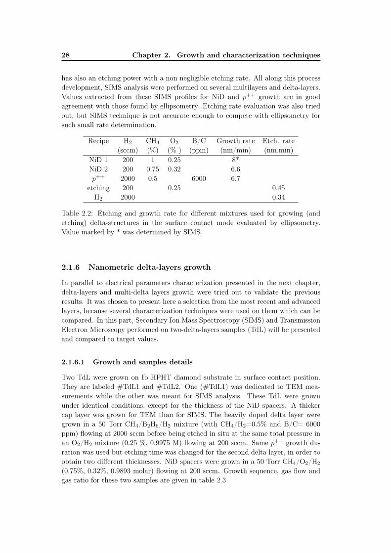
28 Chapter 2. Growth and characterization techniques
has also an etching power with a non negligible etching rate. All along this process
development, SIMS analysis were performed on several multilayers and delta-layers.
Values extracted from these SIMS profiles for NiD and p++ growth are in good
agreement with those found by ellipsometry. Etching rate evaluation was also tried
out, but SIMS technique is not accurate enough to compete with ellipsometry for
such small rate determination.
Recipe H2 CH4 O2 B/C Growth rate Etch. rate
(sccm) (%) (% ) (ppm) (nm/min) (nm.min)
NiD 1 200 1 0.25 8*
NiD 2 200 0.75 0.32 6.6
p++ 2000 0.5 6000 6.7
etching 200 0.25 0.45
H2 2000 0.34
Table 2.2: Etching and growth rate for different mixtures used for growing (and
etching) delta-structures in the surface contact mode evaluated by ellipsometry.
Value marked by * was determined by SIMS.
2.1.6 Nanometric delta-layers growth
In parallel to electrical parameters characterization presented in the next chapter,
delta-layers and multi-delta layers growth were tried out to validate the previous
results. It was chosen to present here a selection from the most recent and advanced
layers, because several characterization techniques were used on them which can be
compared. In this part, Secondary Ion Mass Spectroscopy (SIMS) and Transmission
Electron Microscopy performed on two-delta-layers samples (TdL) will be presented
and compared to target values.
2.1.6.1 Growth and samples details
Two TdL were grown on Ib HPHT diamond substrate in surface contact position.
They are labeled #TdL1 and #TdL2. One (#TdL1) was dedicated to TEM mea-
surements while the other was meant for SIMS analysis. These TdL were grown
under identical conditions, except for the thickness of the NiD spacers. A thicker
cap layer was grown for TEM than for SIMS. The heavily doped delta layer were
grown in a 50 Torr CH4/B2H6/H2 mixture (with CH4/H2=0.5% and B/C= 6000
ppm) flowing at 2000 sccm before being etched in situ at the same total pressure in
an O2/H2 mixture (0.25 %, 0.9975 M) flowing at 200 sccm. Same p++ growth du-
ration was used but etching time was changed for the second delta layer, in order to
obtain two different thicknesses. NiD spacers were grown in a 50 Torr CH4/O2/H2
(0.75%, 0.32%, 0.9893 molar) flowing at 200 sccm. Growth sequence, gas flow and
gas ratio for these two samples are given in table 2.3

2.1. Epilayer growth and characterization 29
Step Plasma Flow CH4/H2 O2/H2 B/C #TdL1 #TdL2
(sccm) (%) (%) (ppm) (min) (min)
1 H2 200 120 120
2 NiD 200 0.75 0.32 33 33
3 H2 2000 3 3
4 p++ 2000 0.5 6000 1 1
5 H2 2000 3 3
6 O2/H2 200 0.25 6 6
7 H2 2000 3 3
8 NiD 200 0.75 0.32 11 11
9 H2 2000 3 3
10 p++ 2000 0.5 6000 1 1
11 H2 2000 3 3
12 O2/H2 200 0.25 7 7
13 H2 2000 3 3
14 NiD 200 0.75 0.32 33 11
Table 2.3: Growth sequences with gas flow, gas ratio and duration of each step for
the two-delta-layers #TdL1 and #TdL2.
2.1.6.2 Characterization results
Typical nanometric scale delta layer were introduced in sample #TdL1 and #TdL2.
The thinner delta layer labeled ↵ was etched for a longer time than the one labeled
β (respectively step 6 and 12 in table 2.3).
Figure 2.6: HAADF observa-
tion of delta-layers along [100]
zone axis (a) and HAADF
images of both top (b) and
bottom (c) layers.
Figure 2.6 displays HAADF images of #TdL1 where the two delta layers can been
distinguished: darker than the NiD part. The grey scale "noise" of this HAADF
image was attributed to amorphous superficial over layers and to local lamella thick-

30 Chapter 2. Growth and characterization techniques
ness variations [Araùjo 2013]. As can be seen on each zoomed image in Fig. 2.6 (c)
and (d), the nanometric scale was reached. Normalized HAADF intensity integrated
over the width of the dash lined rectangle in Fig. 2.6 (a) was plotted in Fig. 2.7
(a). Thickness of each delta layer was estimated at Full Width at Half Maximum
(FWHM) to 2.2 nm for delta ↵ and 3.2 nm for delta β.
Figure 2.7: (a) Normalized HAADF intensity versus depth of 2 delta-layers of
#TdL1 where top layer ↵ and bottom layer β show respectively a 2.2 nm and 3.2
nm thickness in FWHM and (b) boron profile obtained by SIMS analysis of #TdL2
grown under the same conditions.
SIMS analysis of sample #TdL2 where the two delta layers were grown in the same
conditions than #TdL1 is shown in Fig. 2.7 (b). In the case of very thin and heavily
doped layers such as delta layer, it has been shown that ion mixing and low reso-
lution can lead to erroneous values of thickness and doping level on the raw SIMS
profile except if the Depth Resolution Function (DRF) is known and computed with
2.1. Epilayer growth and characterization 31
the SIMS data to obtain a corrected SIMS profile [Fiori 2013a, Fiori 2013b]. Boron
depth profile (15 keV, Cs+ as primary ions at an incident angle of 27) was fitted
using the DRF determined from experiment with isotopic carbon on another delta
layer as described in Ref. [Fiori 2013b]. The results confirmed the expected values
for the thickness (1 nm for ↵ and 2 nm for β) and the atomic concentration for both
the boron-delta-layers ([B] = 1.2 1021 cm−3). As the depth sampling of SIMS
analysis is in the same order than the delta layers thickness, it was not possible
to evaluate the interface thickness. This point can explain the difference between
thicknesses values determined by HAADF at FWHM and by SIMS analysis. To be
more accurate, SIMS analysis should be performed with lower energy primary ion
such as the one shown on Fig. 2.7 (b) at 1 keV, but unfortunately the DRF has not
been yet determined for such conditions.
It is also possible to estimate the thickness of delta layers from growth durations
of table 2.3 and growth and etching rate determined in table 2.2. Both the etching
step (O2/H2) and the H2 rinsing step (3 min before just after p++ growth and 3
min after O2/H2 etching) have to be considered as etching stages. This gives for ↵
and β delta layers thickness of 1.5 nm and 2.0 nm respectively. These values are in
good agreement with the thicknesses deduced by the de-convoluted SIMS profile. It
seems, as it has been already told, that such values lie in a thickness range where
the roughness, the homogeneity of the layer and also the measurements accuracy
could have an influence.
2.1.7 Diamond epilayer for MOS structure
The same reactor than for delta structures growth was used to grow epilayer for
MOS capacitor. The active layer (called p− for low doped) was grown in a 50 Torr
CH4/B2H6/H2 mixture flowing at 200 sccm with CH4/H2 =2 % and B/C= 2 ppm.
These conditions yield layers with a doping level of a few 1017 cm−3. A first MOS
structure was fabricated on such a layer where no oxygen was added in the gas phase.
As the results were promising, it was decided to keep this recipe at least in the first
round. In future investigations, it is not excluded to vary growth parameters during
the device optimization step.
In some of the MOS capacitors investigated in this work, a buried p++ layer aimed
at reducing the series resistance was added (as will be explained in chapter 4). Con-
trary to delta-layer, an accurate control of the thickness is not required, thus growth
condition favoring better boron incorporation with an higher growth rate was cho-
sen: a CH4/B2H6/H2 mixture (with CH4/H2=4% and B/C=1200 ppm) flowing at
100 sccm.
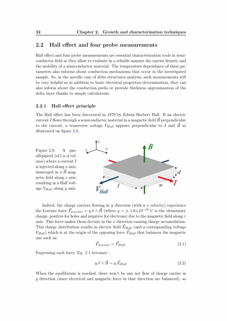
32 Chapter 2. Growth and characterization techniques
2.2 Hall effect and four probe measurements
Hall effect and four probe measurements are essential characterization tools in semi-
conductor field as they allow to evaluate in a reliable manner the carrier density and
the mobility of a semiconductor material. The temperature dependance of these pa-
rameters also informs about conduction mechanisms that occur in the investigated
sample. So, in the specific case of delta structures analysis, such measurements will
be very helpful as in addition to basic electrical properties determination, they can
also inform about the conduction paths or provide thickness approximation of the
delta layer thanks to simple calculations.
2.2.1 Hall effect principle
The Hall effect has been discovered in 1879 by Edwin Herbert Hall. If an electric
current I flows through a semiconductor material in a magnetic field ~B perpendicular
to the current, a transverse voltage VHall appears perpendicular to I and ~B as
illustrated on figure 2.8.
Figure 2.8: A par-
allepipoid (of l.w.d vol-
ume) where a current I
is injected along x axis,
immerged in a ~B mag-
netic field along z axis,
resulting in a Hall volt-
age VHall along y axis.
z !
x!y ! B !
I !VHall !
l! w!
d !
Indeed, the charge carriers flowing in y direction (with a v velocity) experience
the Lorentz force ~FLorentz = q.~v ^ ~B (where q = ± 1.610−19 C is the elementary
charge, positive for holes and negative for electrons) due to the magnetic field along z
axis. This force makes them deviate in the x direction causing charge accumulation.
This charge distribution results in electric field ~EHall (and a corresponding voltage
VHall) which is at the origin of the opposing force ~FHall that balances the magnetic
one such as:~FLorentz = ~FHall. (2.1)
Expressing each force, Eq. 2.1 becomes :
q.~v ^ ~B = q. ~EHall (2.2)
When the equilibrium is reached, there won’t be any net flow of charge carrier in
y direction (since electrical and magnetic force in that direction are balanced), so
2.2. Hall effect and four probe measurements 33
that the Lorentz force has only an y component. Consequently, a scalar equation
can be used :
FLorentz,y = −qvx.Bz (2.3)
and thus the ~EHall electric field has also only a y component noted EHall. The
current total density is jx = q.n.vx with n the number of charge carriers. Therefore
it can be written that :
q.EHall = qvx.Bz =q.Bz.jxq.n
. (2.4)
The Hall coefficient KH is defined by :
KH =EHall
jxB=
1
q.n(2.5)
In practice, the Hall voltage is measured and can be expressed from eq.2.4 and
electric field expression EHall = VHall/w as :
VHall =w
n.q.jx.Bz (2.6)
The current Ix is related to the current density by jx = Ix/w.d and so, the Hall
voltage expression becomes :
VHall =Ix.Bz
q.n.1
d=
KH .Ix.Bz
d(2.7)
where d is the thickness of the sample. Introducing nS the sheet carrier density in
[m−2] which takes in account d, the Hall voltage becomes :
VHall =I.B
q.nS(2.8)
As in most of the cases d is not known, a sheet Hall coefficient KS = 1/q.nS is
usually defined such as :
VHall = KS .I.B (2.9)
Measuring VHall and knowing I and B allow to determine the type of charge carrier
from the sign of KS (< 0 for electrons and > 0 for holes) and the Hall sheet carrier
density since nS = 1/q.KS . The thickness of the layer must be known to determine
the 3D carrier density.
It has to be noted that the calculations above were made under simplifying as-
sumptions of energy independent scattering mechanisms. The exact expression for
the Hall coefficient is :
KH =rHq.n
(2.10)
where rH is the Hall factor and varies between 1 and 2 depending the main scatter-
ing mechanism. In this work, this factor will be assumed equal to 1 since its exact

34 Chapter 2. Growth and characterization techniques
value in diamond is not known as function of doping and temperature.
Let’s still consider the geometry described in Fig. 2.8. Combining this nS mea-
surement with a sheet resistance RS (RS = /d = 1/(q.n.µ.d) = 1/(q.nS .µ)) mea-
surement permits to determine the mobility since:
KS
RS=
q.nS .µ
q.nS= µ (2.11)
It must be noticed that in this work, the thickness of the delta layer is not well known
and defined, so, nS will be more relevant that n. Furthermore, µ is determined
without hypothesis on thickness value. Using the theoretical basis exposed above,
the practical determination of these physical quantities will be detailed in the next
two subsections.
2.2.2 Sheet carrier density measurements
Usually the two most popular structures for Hall effect and four probe measure-
ments are Van der Pauw (4 contacts) and Hall bar (5 contacts). In this work, Hall
bar structures have been chosen for their higher reliability and better resolution.
This is the reason why the measurements principle will be only presented for this
type of geometry. If needed, details on Van der Pauw structure can be found in the
literature [Look 1989].
1 2
3
4
1 2
3
4
B !
(b) (a)
I! I
VHall!
Figure 2.9: Schematics of a Hall bar showing the equipotential lines (in blue) when
a current I is injected between contact 1 and 3 (a) without any magnetic field and
(b) with a ~B magnetic field perpendicular to the surface.
On the Hall bars represented on figure 2.9, the current I is injected between contact
1 and 3, which are usually named "injectors". The resultant equipotential lines are
perpendicular to the direction of current as can be seen on Fig. 2.9 (a) where they
2.2. Hall effect and four probe measurements 35
are represented by blue lines. Since contacts 2 and 4 are aligned with the same an
equipotential line, no potential difference (VHall) should be measured between these
two contacts. Upon a magnetic field perpendicular to the surface (Fig. 2.9 (b)),
equipotential lines are no longer perpendicular to the current flow direction (due to
the accumulation of charge on one side of the hall bar), and a voltage difference is
measured between probes 2 and 4: this is the Hall voltage VHall = KS .I.B. There-
fore, sheet carrier density can be obtained from: nS = 1/q.KS
In practice, contact 2 and 4 may not be perfectly aligned. Even without mag-
netic field V24 6= 0 and is equal to an offset voltage Voffset due to the misalignment
of the probes. Even if the Hall bar lithography permits to obtain low offset voltage,
a technique must be used to remove its contribution to the Hall signal. Voffset can
be expressed as a function of the current I flowing in the hall bar by introducing the
corresponding resistance Roffset such as Voffset = Roffset.I. Upon magnetic field,
this offset voltage is added to the Hall voltage such as:
V24 = VHall + Voffset = KH .I.B + Voffset = KH .I.B +Roffset.I (2.12)
To get rid of this problem, four different measurements must be performed :
V24(+I,+B) = +KH .I.B +Roffset.I, (2.13)
V24(−I,+B) = −KH .I.B −Roffset.I, (2.14)
V24(+I,−B) = −KH .I.B +Roffset.I, (2.15)
V24(−I,−B) = +KH .I.B −Roffset.I. (2.16)
Thus the hall voltage can be extracted from equations 2.13, 2.14, 2.15 and 2.16 as
follows :
VHall = KS .I.B =V24(+I,+B)− V24(−I,+B)− V24(+I,−B) + V24(−I,−B)
4(2.17)
where Roffset.I contribution has been removed.
2.2.3 Resistivity and mobility measurements
In order to extract the mobility value, the sheet resistance must be measured. A
fifth contact (labeled 5) is used on the Hall bar in order to measure the resistivity
between 4 and 5 while injecting current between 1 and 3 (see Fig. 2.10) such as:
R13,45 =V45
I13(2.18)
This is called a four probe resistivity measurement and has the advantage to get
rid of the contact resistance. The contact labeled 6 is only used in case of failure of
another one. For the geometry described on Fig. 2.10 :
R13,45 =.l
S=
.l
w.d(2.19)
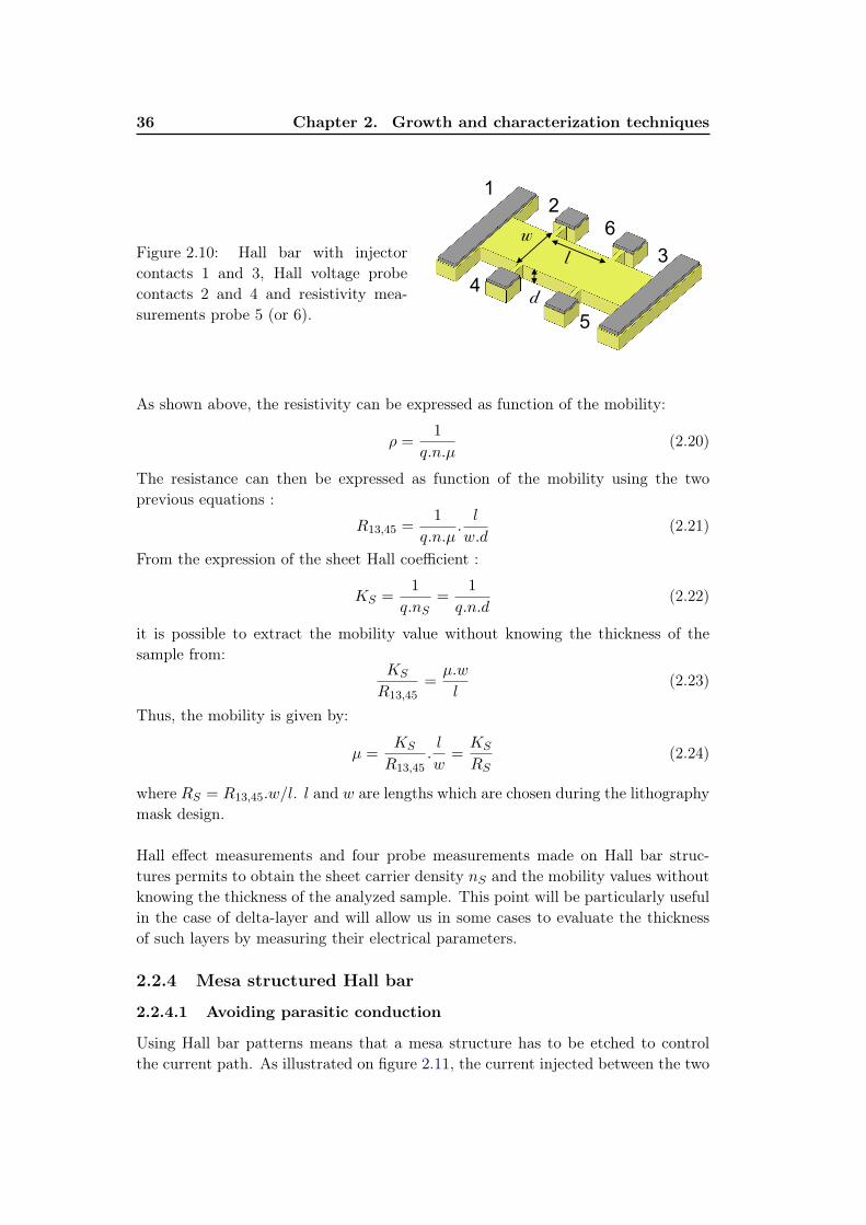
36 Chapter 2. Growth and characterization techniques
Figure 2.10: Hall bar with injector
contacts 1 and 3, Hall voltage probe
contacts 2 and 4 and resistivity mea-
surements probe 5 (or 6).d!
l !
w !
1 2
3
4
5
6
As shown above, the resistivity can be expressed as function of the mobility:
=1
q.n.µ(2.20)
The resistance can then be expressed as function of the mobility using the two
previous equations :
R13,45 =1
q.n.µ.l
w.d(2.21)
From the expression of the sheet Hall coefficient :
KS =1
q.nS=
1
q.n.d(2.22)
it is possible to extract the mobility value without knowing the thickness of the
sample from:KS
R13,45=
µ.w
l(2.23)
Thus, the mobility is given by:
µ =KS
R13,45.l
w=
KS
RS(2.24)
where RS = R13,45.w/l. l and w are lengths which are chosen during the lithography
mask design.
Hall effect measurements and four probe measurements made on Hall bar struc-
tures permits to obtain the sheet carrier density nS and the mobility values without
knowing the thickness of the analyzed sample. This point will be particularly useful
in the case of delta-layer and will allow us in some cases to evaluate the thickness
of such layers by measuring their electrical parameters.
2.2.4 Mesa structured Hall bar
2.2.4.1 Avoiding parasitic conduction
Using Hall bar patterns means that a mesa structure has to be etched to control
the current path. As illustrated on figure 2.11, the current injected between the two
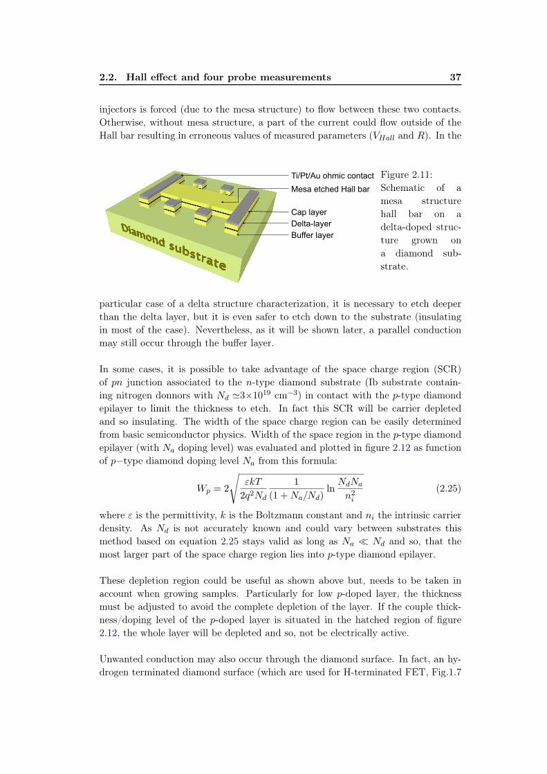
2.2. Hall effect and four probe measurements 37
injectors is forced (due to the mesa structure) to flow between these two contacts.
Otherwise, without mesa structure, a part of the current could flow outside of the
Hall bar resulting in erroneous values of measured parameters (VHall and R). In the
Ti/Pt/Au ohmic contact
Mesa etched Hall bar
Delta-layer
Buffer layer
Cap layer
Figure 2.11:
Schematic of a
mesa structure
hall bar on a
delta-doped struc-
ture grown on
a diamond sub-
strate.
particular case of a delta structure characterization, it is necessary to etch deeper
than the delta layer, but it is even safer to etch down to the substrate (insulating
in most of the case). Nevertheless, as it will be shown later, a parallel conduction
may still occur through the buffer layer.
In some cases, it is possible to take advantage of the space charge region (SCR)
of pn junction associated to the n-type diamond substrate (Ib substrate contain-
ing nitrogen donnors with Nd '31019 cm−3) in contact with the p-type diamond
epilayer to limit the thickness to etch. In fact this SCR will be carrier depleted
and so insulating. The width of the space charge region can be easily determined
from basic semiconductor physics. Width of the space region in the p-type diamond
epilayer (with Na doping level) was evaluated and plotted in figure 2.12 as function
of p−type diamond doping level Na from this formula:
Wp = 2
s
"kT
2q2Nd
1
(1 +Na/Nd)ln
NdNa
n2i
(2.25)
where " is the permittivity, k is the Boltzmann constant and ni the intrinsic carrier
density. As Nd is not accurately known and could vary between substrates this
method based on equation 2.25 stays valid as long as Na Nd and so, that the
most larger part of the space charge region lies into p-type diamond epilayer.
These depletion region could be useful as shown above but, needs to be taken in
account when growing samples. Particularly for low p-doped layer, the thickness
must be adjusted to avoid the complete depletion of the layer. If the couple thick-
ness/doping level of the p-doped layer is situated in the hatched region of figure
2.12, the whole layer will be depleted and so, not be electrically active.
Unwanted conduction may also occur through the diamond surface. In fact, an hy-
drogen terminated diamond surface (which are used for H-terminated FET, Fig.1.7
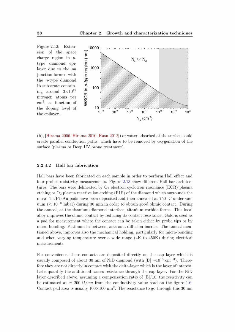
38 Chapter 2. Growth and characterization techniques
Figure 2.12: Exten-
sion of the space
charge region in p-
type diamond epi-
layer due to the pn
junction formed with
the n-type diamond
Ib substrate contain-
ing around 31019
nitrogen atoms per
cm3, as function of
the doping level of
the epilayer. 1014
1015
1016
1017
1018
1019
1020
10
100
1000
10000
WS
CR
in p-type r
egio
n (
nm
)
NA (cm
-3)
Na << Nd!
(b), [Hirama 2006, Hirama 2010, Kasu 2012]) or water adsorbed at the surface could
create parallel conduction paths, which have to be removed by oxygenation of the
surface (plasma or Deep UV ozone treatment).
2.2.4.2 Hall bar fabrication
Hall bars have been fabricated on each sample in order to perform Hall effect and
four probes resistivity measurements. Figure 2.13 show different Hall bar architec-
tures. The bars were delineated by O2 electron cyclotron resonance (ECR) plasma
etching or O2 plasma reactive ion etching (RIE) of the diamond which surrounds the
mesa. Ti/Pt/Au pads have been deposited and then annealed at 750 C under vac-
uum (< 10−8 mbar) during 30 min in order to obtain good ohmic contact. During
the anneal, at the titanium/diamond interface, titanium carbide forms. This local
alloy improves the ohmic contact by reducing its contact resistance. Gold is used as
a pad for measurement where the contact can be taken either by probe tips or by
micro-bonding. Platinum in between, acts as a diffusion barrier. The anneal men-
tioned above, improves also the mechanical holding, particularly for micro-bonding
and when varying temperature over a wide range (4K to 450K) during electrical
measurements.
For convenience, these contacts are deposited directly on the cap layer which is
usually composed of about 30 nm of NiD diamond (with [B] 1016 cm−3). There-
fore they are not directly in contact with the delta-layer which is the layer of interest.
Let’s quantify the additional access resistance through the cap layer. For the NiD
layer described above, assuming a compensation ratio of [B]/10, the resistivity can
be estimated at ' 200 Ω/cm from the conductivity value read on the figure 1.6.
Contact pad area is usually 100100 µm2. The resistance to go through this 30 nm

2.2. Hall effect and four probe measurements 39
Figure 2.13: Pictures of different Hall bar architectures fabricated at (a), (b) Institut
Néel, Grenoble and (c) IEMN Lille. On (c) picture Hall bars of different sizes (from
10 µm to 200 µm) can been seen. The inset is a Scanning Electron Microscopy
image of an hall bar of 20 µm length. Other patterns can been seen on this sample :
Transmission Line Measurements patterns and also Field Effect Transistors without
gate insulator.
layer of ' 200 Ω/cm resistivity is:
Raccess =.L
S= 6 Ω (2.26)
When flowing from a contact toward an other one by passing in the delta-layer,
the current has to cross twice the cap layer. Even considering two times Raccess,
this contribution stays negligible in regards of the delta-layer resistance as it will
be seen in the following. The contact resistance has also to be taken into account.
But, thanks to the post deposition anneal and the large area of the contact, this
resistance is expected to be low.
The surface needs to be passivated to avoid electrical conduction. Parasitic con-
duction occurring through i) hydrogen terminated surface that can be removed by
oxidizing the surface using an UV ozone treatment or/and ii) water adsorbed on
the surface can be avoided by performing measurements under vacuum.
The measurements shown in this PhD work were performed both on Institut Néel
Hall bars (Fig. 2.13 (a) and (b)) and IEMN Hall bars (Fig. 2.13 (c)). On figure
2.13 (c) different sizes of hall bars can be seen from 10 µm to 200 µm that allowed
us to investigate the influence of the Hall bars size on electrical properties, which is
expected to be inexistent.
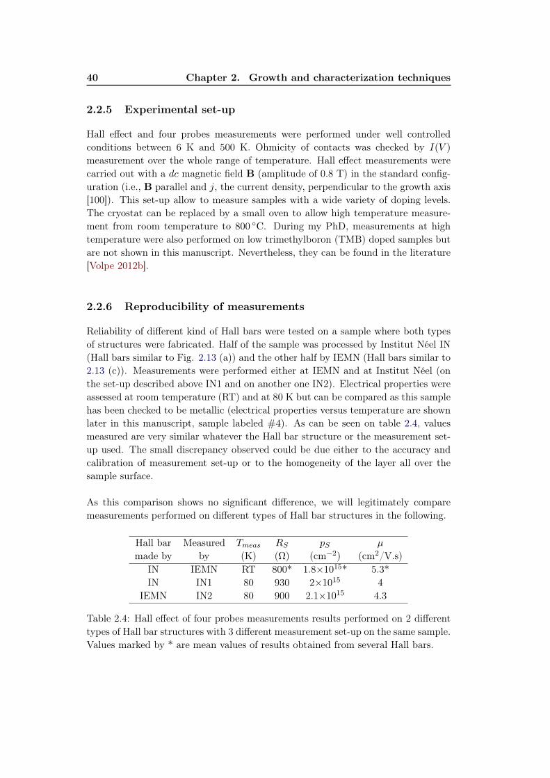
40 Chapter 2. Growth and characterization techniques
2.2.5 Experimental set-up
Hall effect and four probes measurements were performed under well controlled
conditions between 6 K and 500 K. Ohmicity of contacts was checked by I(V )
measurement over the whole range of temperature. Hall effect measurements were
carried out with a dc magnetic field B (amplitude of 0.8 T) in the standard config-
uration (i.e., B parallel and j, the current density, perpendicular to the growth axis
[100]). This set-up allow to measure samples with a wide variety of doping levels.
The cryostat can be replaced by a small oven to allow high temperature measure-
ment from room temperature to 800 C. During my PhD, measurements at high
temperature were also performed on low trimethylboron (TMB) doped samples but
are not shown in this manuscript. Nevertheless, they can be found in the literature
[Volpe 2012b].
2.2.6 Reproducibility of measurements
Reliability of different kind of Hall bars were tested on a sample where both types
of structures were fabricated. Half of the sample was processed by Institut Néel IN
(Hall bars similar to Fig. 2.13 (a)) and the other half by IEMN (Hall bars similar to
2.13 (c)). Measurements were performed either at IEMN and at Institut Néel (on
the set-up described above IN1 and on another one IN2). Electrical properties were
assessed at room temperature (RT) and at 80 K but can be compared as this sample
has been checked to be metallic (electrical properties versus temperature are shown
later in this manuscript, sample labeled #4). As can be seen on table 2.4, values
measured are very similar whatever the Hall bar structure or the measurement set-
up used. The small discrepancy observed could be due either to the accuracy and
calibration of measurement set-up or to the homogeneity of the layer all over the
sample surface.
As this comparison shows no significant difference, we will legitimately compare
measurements performed on different types of Hall bar structures in the following.
Hall bar Measured Tmeas RS pS µ
made by by (K) (Ω) (cm−2) (cm2/V.s)
IN IEMN RT 800* 1.81015* 5.3*
IN IN1 80 930 21015 4
IEMN IN2 80 900 2.11015 4.3
Table 2.4: Hall effect of four probes measurements results performed on 2 different
types of Hall bar structures with 3 different measurement set-up on the same sample.
Values marked by * are mean values of results obtained from several Hall bars.
2.3. Conclusion 41
2.3 Conclusion
In this chapter we show that the growth experimental set-up developed to suit delta-
layer requirements allows us to grow nanometric size delta layers with thickness
down to 1 nm. Such layers lie within the thickness target but what about their
electrical properties ? Four probes and Hall effect measurements appears as powerful
and accurate tools to investigate them. As shown by detailing the measurements
principle, such investigation will give access to sheet resistance, mobility and carrier
density values. The temperature dependence of these physical parameters with
the temperature will allow us to investigate conduction mechanisms involved in
such structures. To sum up, these characterization techniques turn out to be very
powerful but had to be further developed to tackle efficiently the issue of delta-doped
structures.

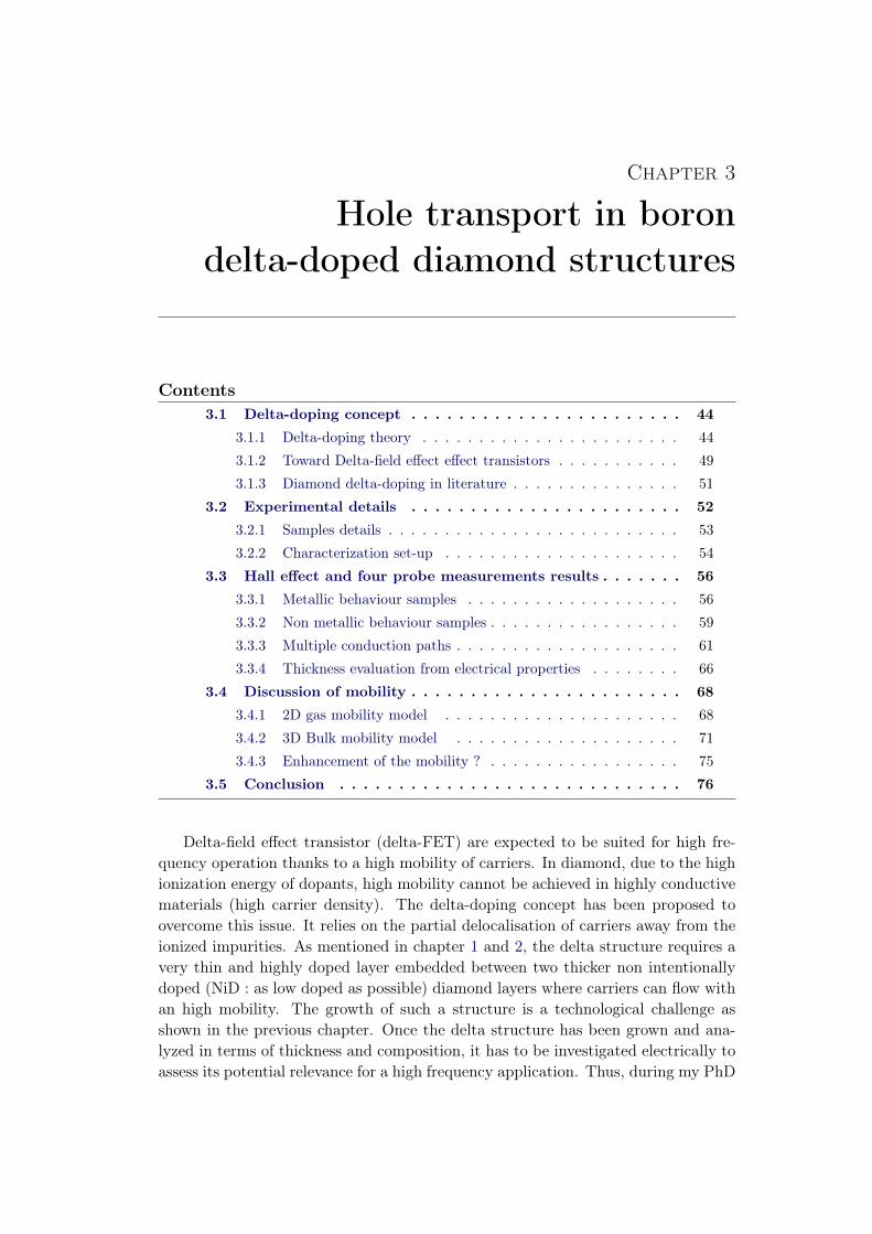
Chapter 3
Hole transport in boron
delta-doped diamond structures
Contents
3.1 Delta-doping concept . . . . . . . . . . . . . . . . . . . . . . . 44
3.1.1 Delta-doping theory . . . . . . . . . . . . . . . . . . . . . . . 44
3.1.2 Toward Delta-field effect effect transistors . . . . . . . . . . . 49
3.1.3 Diamond delta-doping in literature . . . . . . . . . . . . . . . 51
3.2 Experimental details . . . . . . . . . . . . . . . . . . . . . . . 52
3.2.1 Samples details . . . . . . . . . . . . . . . . . . . . . . . . . . 53
3.2.2 Characterization set-up . . . . . . . . . . . . . . . . . . . . . 54
3.3 Hall effect and four probe measurements results . . . . . . . 56
3.3.1 Metallic behaviour samples . . . . . . . . . . . . . . . . . . . 56
3.3.2 Non metallic behaviour samples . . . . . . . . . . . . . . . . . 59
3.3.3 Multiple conduction paths . . . . . . . . . . . . . . . . . . . . 61
3.3.4 Thickness evaluation from electrical properties . . . . . . . . 66
3.4 Discussion of mobility . . . . . . . . . . . . . . . . . . . . . . . 68
3.4.1 2D gas mobility model . . . . . . . . . . . . . . . . . . . . . 68
3.4.2 3D Bulk mobility model . . . . . . . . . . . . . . . . . . . . 71
3.4.3 Enhancement of the mobility ? . . . . . . . . . . . . . . . . . 75
3.5 Conclusion . . . . . . . . . . . . . . . . . . . . . . . . . . . . . 76
Delta-field effect transistor (delta-FET) are expected to be suited for high fre-
quency operation thanks to a high mobility of carriers. In diamond, due to the high
ionization energy of dopants, high mobility cannot be achieved in highly conductive
materials (high carrier density). The delta-doping concept has been proposed to
overcome this issue. It relies on the partial delocalisation of carriers away from the
ionized impurities. As mentioned in chapter 1 and 2, the delta structure requires a
very thin and highly doped layer embedded between two thicker non intentionally
doped (NiD : as low doped as possible) diamond layers where carriers can flow with
an high mobility. The growth of such a structure is a technological challenge as
shown in the previous chapter. Once the delta structure has been grown and ana-
lyzed in terms of thickness and composition, it has to be investigated electrically to
assess its potential relevance for a high frequency application. Thus, during my PhD
44 Chapter 3. Hole transport in boron delta-doped diamond structures
thesis, in parallel to the growth process development yielding the delta structures
(presented in chapter 2), an important effort was devoted to their characterization
by Hall effect and four probe resistivity measurements.
In this chapter, the temperature dependence of the electrical transport properties of
diamond delta structures will be presented and discussed in order to evaluate reliably
the carriers mobility and density. These data will be compared to those reported
in the literature and discussed in view of results provided by other characterization
techniques. Two types of conduction were detected, metallic and non metallic, and
a typical mobility value was attributed to each. The measured mobility values will
be discussed and compared to theoretical calculated values. A double conduction
paths was observed and will be also discussed. Prior to that, building on numerical
simulations, we will focus on the principles governing the delta-doping concept. We
will also present key points for the future delta-FET and draw a brief state of the
art of delta-layers electrical characterization.
3.1 Delta-doping concept
As the delta doping relies on delocalisation of holes from the diamond valence bands,
these must be known accurately.
As a prerequisit, the diamond band structure:
Diamond topmost valence bands dispersion have been studied experimentally and
theoretically by several groups. Solid results, thanks to the use of linear muffin-tin-
orbital method in local-density approximation, were obtained by Willatzen et al.
[Willatzen 1994]. They show that the three uppermost valence bands have their
maximum localized at the Γ point of the Brillouin zone. Among these three, the
two upper, named ligh holes (lh) and the heavy holes (hh) are degenerated at the Γ
point and are energetically positioned higher than the third hole band due to the spin
orbit coupling (13 meV), which is named here: spin orbit band (so). For the sake of
simplicity, the small energy gap between the lh, hh and so valence bands is not taken
into account in this work and the three bands are considered degenerated in the Γ
point of the Brillouin zone. The three valence bands are considered to be parabolic.
The values for the density of state mass calculated from the representative masses
given in [Willatzen 1994] are m
hh= 0.588 m0, m
lh= 0.303 m0 and m
so= 0.394 m0
and the total density of state mass is m = (m3/2lh +m
3/2hh +m
3/2so )2/3 =0.908 m0.
Recently reported experimental values [Naka 2013] : m
hh= 0.667 m0, m
lh= 0.264
m0 and m
so= 0.375 m0 confirm the values calculated by Willatzen et al..
3.1.1 Delta-doping theory
Obtaining a single atomic thick boron doped layer would be impossible due to tech-
nical limitations such as initial roughness of diamond substrate. So, boron atoms
will be distributed over a larger thickness with different distribution shape : top
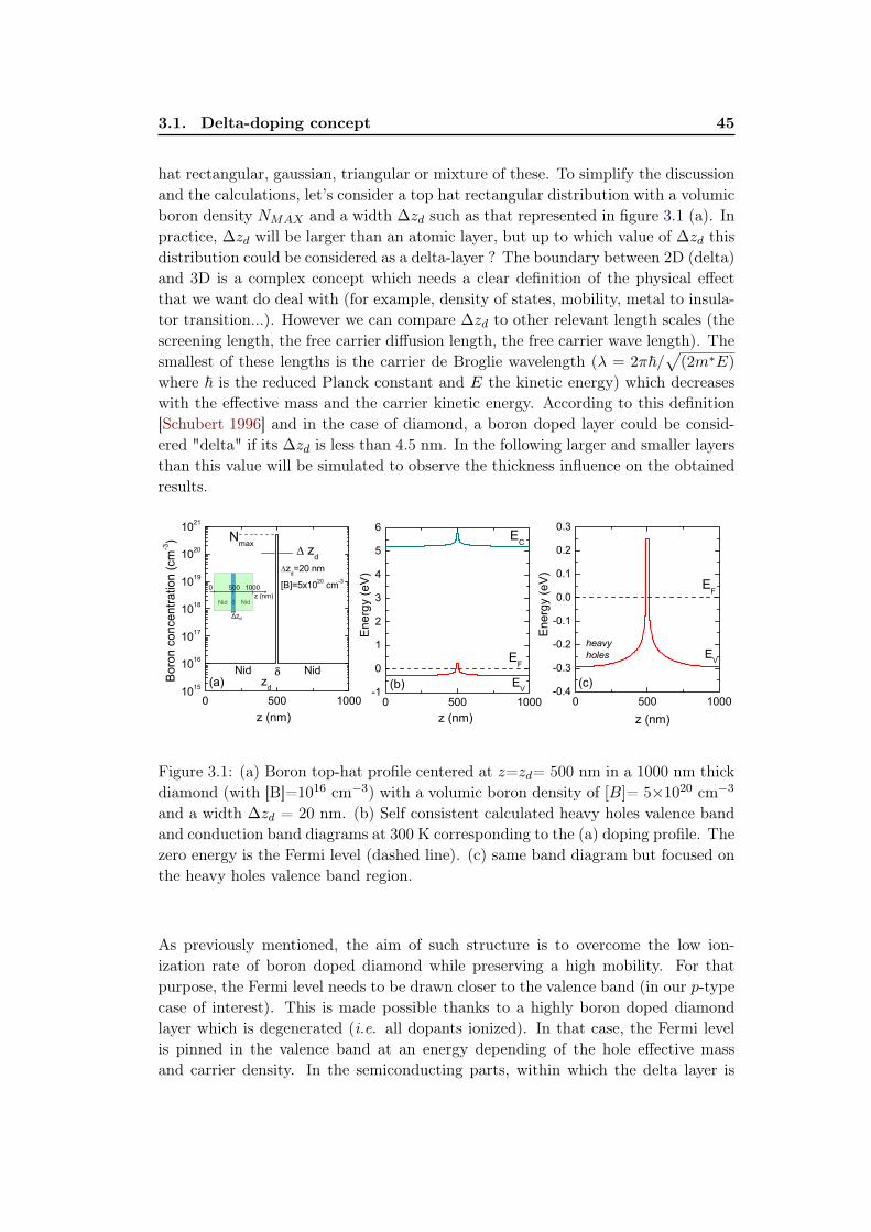
3.1. Delta-doping concept 45
hat rectangular, gaussian, triangular or mixture of these. To simplify the discussion
and the calculations, let’s consider a top hat rectangular distribution with a volumic
boron density NMAX and a width ∆zd such as that represented in figure 3.1 (a). In
practice, ∆zd will be larger than an atomic layer, but up to which value of ∆zd this
distribution could be considered as a delta-layer ? The boundary between 2D (delta)
and 3D is a complex concept which needs a clear definition of the physical effect
that we want do deal with (for example, density of states, mobility, metal to insula-
tor transition...). However we can compare ∆zd to other relevant length scales (the
screening length, the free carrier diffusion length, the free carrier wave length). The
smallest of these lengths is the carrier de Broglie wavelength (λ = 2~/p
(2mE)
where ~ is the reduced Planck constant and E the kinetic energy) which decreases
with the effective mass and the carrier kinetic energy. According to this definition
[Schubert 1996] and in the case of diamond, a boron doped layer could be consid-
ered "delta" if its ∆zd is less than 4.5 nm. In the following larger and smaller layers
than this value will be simulated to observe the thickness influence on the obtained
results.
0 500 1000
z (nm)
!zd
Nid Nid "
Figure 3.1: (a) Boron top-hat profile centered at z=zd= 500 nm in a 1000 nm thick
diamond (with [B]=1016 cm−3) with a volumic boron density of [B]= 51020 cm−3
and a width ∆zd = 20 nm. (b) Self consistent calculated heavy holes valence band
and conduction band diagrams at 300 K corresponding to the (a) doping profile. The
zero energy is the Fermi level (dashed line). (c) same band diagram but focused on
the heavy holes valence band region.
As previously mentioned, the aim of such structure is to overcome the low ion-
ization rate of boron doped diamond while preserving a high mobility. For that
purpose, the Fermi level needs to be drawn closer to the valence band (in our p-type
case of interest). This is made possible thanks to a highly boron doped diamond
layer which is degenerated (i.e. all dopants ionized). In that case, the Fermi level
is pinned in the valence band at an energy depending of the hole effective mass
and carrier density. In the semiconducting parts, within which the delta layer is

46
Chapte
r3.
Hole
transp
ort
inboro
ndelt
a-d
oped
dia
mond
stru
ctu
res
490 500 510
-0.2
-0.1
0.0
0.1
0.2
0.3
490 500 510
-0.2
-0.1
0.0
0.1
0.2
0.3
490 500 510
-0.2
-0.1
0.0
0.1
0.2
0.3
490 500 510
0.0
0.1
0.2
0.3
(d)
heavy
holes
heavy
holesheavy
holes
(c)(b)
EV
EF
ΨΨ* E0
ΨΨ* E1
ΨΨ* E2
z (nm)
Δzd=0.36 nm
[B]=5x10²⁰
cm-3(a)
heavy
holes
Δzd=2 nm
[B]=5x10²⁰
cm-3
z (nm)
Δzd=5 nm
[B]=5x10²⁰
cm-3
z (nm)
Δzd=20 nm
[B]=5x10²⁰
cm-3
Energ
y (
eV
)
z (nm)
490 500 510
0
1x10¹⁹
2x10¹⁹
3x10¹⁹
4x10¹⁹
5x10¹⁹
6x10¹⁹
490 500 510
0
1x10²⁰
2x10²⁰
3x10²⁰
490 500 510
0
1x10²⁰
2x10²⁰
490 500 510
0
1x10¹⁸
2x10¹⁸
3x10¹⁸
4x10¹⁸
(d’)
heavy
holesheavy
holes
E0
E1
E2
z (nm)
Δzd=0.36 nm
[B]=5x10²⁰
cm-3
[B]Δzd= 1.8x10
13cm
-3
(c’)
heavy
holesheavy
holes
E0
E1
E2
z (nm)
Δzd=2 nm
[B]=5x10²⁰
cm-3
[B]Δzd= 10
14cm
-3
(b’)(a’)
E0
E1
E2
z (nm)
Δzd=5 nm
[B]=5x10²⁰
cm-3
[B]Δzd= 2.5x10
14cm
-3
C
oncentr
ation (
cm
-3)
E0
E1
E2
z (nm)
Δzd=20 nm
[B]=5x10²⁰
cm-3
[B]Δzd= 10
15cm
-3
Figure 3.2: (a) Same band diagrams than figure 3.1 (c) but focused on the carrier confined region and with the self-consistent
calculated free carrier distribution corresponding to the three first states E0, E1 and E2. Distribution densities (Ψ(z)Ψ(z)) have
been shifted according to their energy. The zero energy is the Fermi level (dashed line). (b) (c) and (d) are the same than (a) but
for 5 nm, 2nm and 0.36 nm delta layer thickness respectively. (a’), (b’), (c’) and (d’) are the hole concentrations of the three first
states corresponding respectively to (a), (b), (c) and (d).
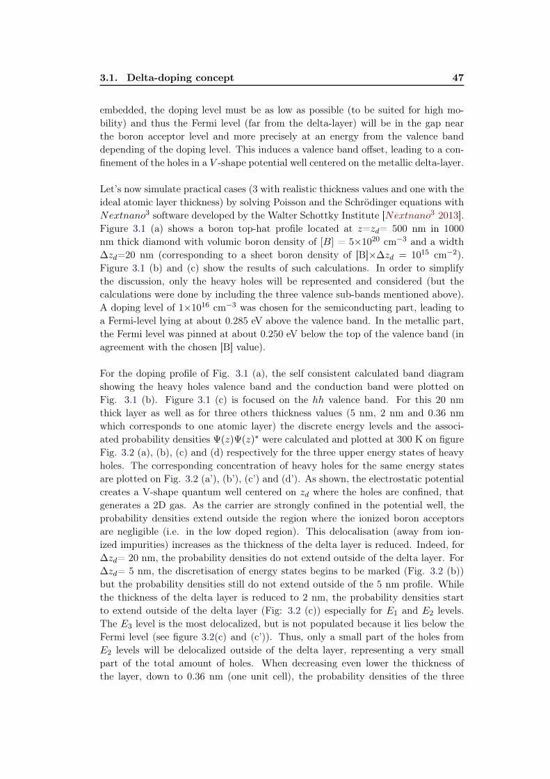
3.1. Delta-doping concept 47
embedded, the doping level must be as low as possible (to be suited for high mo-
bility) and thus the Fermi level (far from the delta-layer) will be in the gap near
the boron acceptor level and more precisely at an energy from the valence band
depending of the doping level. This induces a valence band offset, leading to a con-
finement of the holes in a V -shape potential well centered on the metallic delta-layer.
Let’s now simulate practical cases (3 with realistic thickness values and one with the
ideal atomic layer thickness) by solving Poisson and the Schrödinger equations with
Nextnano3 software developed by the Walter Schottky Institute [Nextnano3 2013].
Figure 3.1 (a) shows a boron top-hat profile located at z=zd= 500 nm in 1000
nm thick diamond with volumic boron density of [B] = 51020 cm−3 and a width
∆zd=20 nm (corresponding to a sheet boron density of [B]∆zd = 1015 cm−2).
Figure 3.1 (b) and (c) show the results of such calculations. In order to simplify
the discussion, only the heavy holes will be represented and considered (but the
calculations were done by including the three valence sub-bands mentioned above).
A doping level of 11016 cm−3 was chosen for the semiconducting part, leading to
a Fermi-level lying at about 0.285 eV above the valence band. In the metallic part,
the Fermi level was pinned at about 0.250 eV below the top of the valence band (in
agreement with the chosen [B] value).
For the doping profile of Fig. 3.1 (a), the self consistent calculated band diagram
showing the heavy holes valence band and the conduction band were plotted on
Fig. 3.1 (b). Figure 3.1 (c) is focused on the hh valence band. For this 20 nm
thick layer as well as for three others thickness values (5 nm, 2 nm and 0.36 nm
which corresponds to one atomic layer) the discrete energy levels and the associ-
ated probability densities Ψ(z)Ψ(z) were calculated and plotted at 300 K on figure
Fig. 3.2 (a), (b), (c) and (d) respectively for the three upper energy states of heavy
holes. The corresponding concentration of heavy holes for the same energy states
are plotted on Fig. 3.2 (a’), (b’), (c’) and (d’). As shown, the electrostatic potential
creates a V-shape quantum well centered on zd where the holes are confined, that
generates a 2D gas. As the carrier are strongly confined in the potential well, the
probability densities extend outside the region where the ionized boron acceptors
are negligible (i.e. in the low doped region). This delocalisation (away from ion-
ized impurities) increases as the thickness of the delta layer is reduced. Indeed, for
∆zd= 20 nm, the probability densities do not extend outside of the delta layer. For
∆zd= 5 nm, the discretisation of energy states begins to be marked (Fig. 3.2 (b))
but the probability densities still do not extend outside of the 5 nm profile. While
the thickness of the delta layer is reduced to 2 nm, the probability densities start
to extend outside of the delta layer (Fig: 3.2 (c)) especially for E1 and E2 levels.
The E3 level is the most delocalized, but is not populated because it lies below the
Fermi level (see figure 3.2(c) and (c’)). Thus, only a small part of the holes from
E2 levels will be delocalized outside of the delta layer, representing a very small
part of the total amount of holes. When decreasing even lower the thickness of
the layer, down to 0.36 nm (one unit cell), the probability densities of the three

48 Chapter 3. Hole transport in boron delta-doped diamond structures
levels extend outside of the delta layer (Fig. 3.2 (d)) but only the E0 level is pop-
ulated. Nevertheless, as shown on Fig. 3.2 (d’) an important amount of holes from
this level is delocalized out of the delta layer while the ionized impurities are still
localized in the delta layer. In that case, an improvement of the mobility is expected.
It has to be noted that only the three first energy states for the hh valence band were
plotted on figure 3.2. But in the case of the two widest delta layer, higher energy
states are populated. Indeed, for the 5 nm and 20 nm thick, 4 and 13 energy states
corresponding to the hh valence bands were respectively populated. In addition,
energy states corresponding to the two other valence sub-bands are also populated,
even if they were not plotted here, for sake of clarity. To illustrate that, the den-
sities of states (DOS) taking into account the three valences bands are plotted on
figure 3.3. It can clearly be seen that for the thinnest layer, the DOS are step-like
which is typical of 2D system, while for the widest layer (20 nm) as several levels
are populated the DOS begins to be similar to the one of a 3D system (DOS /pE
as represented by the grey plot on Fig. 3.3).
Figure 3.3: Density of states
(DOS) calculated for four delta
layers of 0.36 nm, 2 nm, 5 nm,
20 nm of thickness with [B]
= 51020 cm−3 corresponding
to sheet carrier density of
1015 cm−2, 2.51014 cm−2,
1014 cm−2 and 1.81013 cm−2
respectively. The DOS was
calculated taking into account
the three valence sub-bands.
0 50 100 150 200 250
0.0
2.0x10¹⁹
4.0x10¹⁹
6.0x10¹⁹
Δzd = 0.36 nm
Δzd = 2 nm
Δzd = 5 nm
Δzd = 20 nm
EF
Density o
f sta
tes (
eV
-1m
-2)
E (meV)
α E1/2
These calculations show and confirm that layers as thin as or thinner than 2 nm
must be grown to expect observing enhancement of mobility due to delocalisation
of carriers. These results are in good agreement with Fiori et al. work [Fiori 2010]
where it has also been shown that the boron doping level has a weak influence on
the fraction of delocalized holes, as long as the doping level is high enough to ensure
metallic conductivity.

3.1. Delta-doping concept 49
3.1.2 Toward Delta-field effect effect transistors
According to the simulation results presented above, mobility enhancement can be
obtained only for a thickness lower than 2 nm. However, in the case of the delta-field
effect transistor (delta-FET) other parameters than the thickness have to be taken
in account.
3.1.2.1 Delta-FET architecture
A delta-FET in its simplest form is represented on 3.4. In this architecture, the role
of the channel is played by the delta layer. This delta layer is grown on a thick NiD
layer called buffer layer and covered by a thinner NiD layer called cap layer. The
drain and source are ohmic contacts which connect the delta layer channel through
the cap layer. For matter of convenience, these contacts are directly deposited on
the cap layer before being annealed to reduce the contact resistance by forming a
titanium-carbide at the interface. Therefore the drain and source are connected to
the delta layer through the cap layer but as it has been shown in section 2.2.4.2,
thanks to the low thickness of the cap layer and macroscopic contact size, the in-
duced access resistance is negligible with respect to the resistance of the channel.
The conduction of the channel is controlled by a gate which is a Schottky contact
deposited on NiD cap layer. If sufficiently thin delta layers are obtained, delta-FET
Drain Gate Source
Cap layer
Buffer layer
ddelta
dcap
delta layer
Diamond substrate
Figure 3.4: Schematic
of a diamond delta
field effect transistor
in its simplest form.
combining high carrier concentration and high mobility could be achieved. Such a
transistor, as represented on figure 3.4 (d), would be on in the normal state when
no voltage is applied on the gate and off for an applied positive voltage. In fact,
if the cap layer and the delta layer are depleted of charge carrier under the gate,
the current should not flow anymore between the drain and source electrodes. This
voltage must be high enough to completely deplete the channel in order to have
a good off state. Even if the breakdown field in diamond is higher than in other
semiconductors, the large amount of charges needed to create metallic delta layer
(with [B]> Ncrit(3D)=51020cm−3) counterbalances this high value. Therefore, the
breakdown field of diamond will introduce a limitation for the sheet charge density
that can be depleted in the channel as will be detailed in the following

50 Chapter 3. Hole transport in boron delta-doped diamond structures
3.1.2.2 Breakdown field induced limitation
Looking at the delta-FET of figure 3.4, the stack gate/cap-layer/delta layer could
be considered as a planar capacitance1 where the electric field F is given by:
F =V
dcap(3.1)
where V is the applied voltage on the gate with reference to the drain (or source)
and so to the delta-layer. Thus, V is the applied voltage through the thickness of
the cap layer. The sheet (normalized by area) capacitance C can be written as the
ratio of the charge Q by the voltage V applied on the gate:
C =Q
V(3.2)
where Q is a surface charge. This charge can be expressed as a function of the sheet
carrier density pS of the delta-layer such as:
Q = q.pS (3.3)
with q=e=1.610−19 C the elementary charge as holes are considered here. By
definition the surfacic capacitance is given by :
C ="r"0dcap
(3.4)
where "r the relative permittivity of diamond, "0 the vacuum permittivity. There-
fore, by introducing Eq. 3.4 and 3.3 in 3.2, the voltage V can be written:
V =q.pS .dcap
"r"0(3.5)
If we introduce equation 3.5 in equation 3.1 the electric field as a function of pS is
obtained independently of the cap layer thickness:
F =q.pS"r"0
(3.6)
By doing the numerical application with diamond breakdown field value of 10
MV/cm, the breakdown field is reached for a sheet hole density equal or larger
than 3.2 1013 cm−2. As the delta-layer is made of diamond doped above the
metal to insulator transition, all the boron atoms are ionized such as [B]=pS/ddelta.
Therefore, the boron concentration versus the thickness of the layer as well as the
corresponding breakdown electric field isolines are plotted on figure 3.5. This dia-
gram shows that the working zone where a diamond delta-doped FET channel can
be closed without reaching the maximum breakdown field is very limited. In fact,
in addition to the electric field limitations, low limitation in terms of thickness (by
the lattice constance) and in term of doping (by the MIT) will restrain further this
working zone.
1The intrinsic diamond of the cap layer plays the role of the insulator while the gate metal and
the delta-layer could be considered as the electrodes.

3.1. Delta-doping concept 51
FB = 10 M
V/cm
MIT
Dia
mo
nd la
ttice
co
nsta
nt
Working Zone
0,1 1 10
1E20
1E21
Boro
n c
oncentr
ation (
cm
-3)
Layer thickness d (nm)
Figure 3.5: Boron concentra-
tion versus thickness map with
the corresponding calculated
diamond breakdown field. In
addition, diamond lattice con-
stant and metal insulator tran-
sition are reported. The tri-
angle named "Working Zone"
shows the range of doping level
and thickness eligible for a
delta FET where the channel
can be closed by applying a
voltage without reaching the
breakdown electric field in di-
amond.
It has to be noted that these calculations were done to obtain an order of mag-
nitude of the thickness and of the doping level of a delta layer eligible to be incor-
porated in a delta FET for which the channel could be closed. But assumptions
were made. Indeed, as in bulk diamond, it has been assumed that the boron ion-
ization energy Ea decrease is related to the majority impurity concentration and
follow the Pearson-Bardeen model [Pearson 1949] in which Ea decreases following
Ea = Ea0(1− ([B]/Ncrit(3D))1/3) (as plotted on figure 1.4). This model is based on
the overlapping of wavefunction of the hole bond to acceptor level and in this case
[B]1/3 represents the average boron-boron atoms distance in the lattice [Mott 1949].
The question is opened for Ea versus [B] in the case of two dimensional doping, but
Ncrit(2D) is expected to be larger than Ncrit(3D). Nevertheless, the results obtained
in this work seem to show that the situation is not so different from the three di-
mensional case, as discussed later.
To summarize, delta-layers thinner than 0.64 nm and doped between 5 1020 cm−3
and 1 1021 cm−3 have to be aimed at. A delta-layer theoretically suitable for these
requirements was simulated, the results can be seen in figures 3.2 (d) and (d’). In
these figures, it can be observed that an important part of the holes is delocalized
out of the delta-layer, which would entail a significant improvement of the mobility
if such a layer could be grown. Nevertheless, if a high mobility value can be achieved
in such a structure, even if it is not possible to close the channel in the corresponding
delta- FET, such a device could be used for radio-frequency applications.
3.1.3 Diamond delta-doping in literature
Since delta doping has been proposed in diamond [Kobayashi 1994] as a solution
to overcome high boron dopant ionization energy, a lot of works on diamond delta

52 Chapter 3. Hole transport in boron delta-doped diamond structures
doped structures have been published by several groups, dealing both with the
fabrication and the characterization by electrical measurements. Most of the elec-
tronic properties of the delta structures have been characterized by means of a
field effect transistor (FET) [Aleksov 1999, Elhajj 2008, Scharpf 2013]. Tempera-
ture dependent impedance spectroscopy measurements have also been performed
to identify the different conduction paths in the stacked structures [Tumilty 2009,
Edgington 2012]. Hall effect combined to four probe resistivity measurements have
been also used to measure the sheet density (pS) and the carrier mobility (µH)
[Kunze 1999, Edgington 2012, Balmer 2013, Chicot 2012]. Low sheet density (pS '1013 cm−2) and a hole mobility (µH = 13 cm2/V.s at 300K) larger than the one ex-
pected for highly doped bulk diamond were reported in δ-structures on [111]-oriented
diamond substrates [Edgington 2012]. Unfortunately, no temperature dependence of
pS and µH were shown for the same samples. Recently, Balmer et al. [Balmer 2013]
reported very low mobility at low temperature (µH 0.3 cm2/V.s at 100 K) and
very high mobility at room temperature (µH 900 cm2/V.s) explained by a two
carrier-type model. However the corresponding devices did not yield any improved
performance as the high mobility value measured is not related to the delta-layer
channel. The most recent of this work [Scharpf 2013] reported nanometric delta
layer with pS ' 4 1013 cm−2 (estimated by C(V) and ERD) showing mobility
value about 0.1 cm2.V.s−1 (measured using FET). To explain these very low mobil-
ity values, a transport model combining hopping and tunneling processes between
boron clusters was proposed.
This PhD project is focused on the analysis of temperature dependence of the sheet
resistivity RS , the sheet carrier density pS(T) and the mobility µH(T) of delta struc-
tures to investigate either electrical characteristics and physical properties (such as
doping and thickness) and understand the limitations involved in the low mobilities.
The results will be compared to others techniques such as secondary ion mass spec-
troscopy (SIMS), ellipsometry and transmission electron microscopy (TEM) analy-
sis.
Our investigations about delta structures have been undertaken within the frame-
work of an ANR project called "Deltadiam". In addition to Institut Néel, three
others partners participated to this project : CEA LIST (Saclay), IEMN (Lille)
and ESRF (Grenoble). That is why, results on samples grown by the first partner
and processed by the second one will be also presented in the manuscript, in addition
to those grown and processed at Institut Néel.
3.2 Experimental details
Two types of diamond substrates were used for epitaxy and a sample was also grown
using a different growth set up than the one described in the previous chapter. These
delta structures were assessed electrically by four probe resistivity and Hall effect

3.2. Experimental details 53
measurements.
3.2.1 Samples details
Ten boron doped samples were grown by Microwave Plasma-enhanced Chemical
Vapor Deposition (MPCVD). Samples #1 to #9 were grown in a modified vertical
silica tube NIRIM-type reactor (described in more details chapter 2), where the
volume has been reduced, and an ultra-fast gas switching has been implemented
while a well-controlled in situ plasma etch process was developed [Fiori 2012b]. All
stacks were homo-epitaxially grown on Ib-type [100]-oriented 33 mm2 diamond
substrates (purchased from Sumitomo Electric), except for sample #7, which was
grown on IIa-type [100]-oriented diamond substrates. All samples involve a highly
p-doped ([B] ≥ 5 1020 cm−3) layer of thickness lower than 40 nm grown on a
thick non intentionally doped (NiD) buffer layer suited for high mobility transport
[Volpe 2009, Volpe 2012b] and capped by another thin NiD layer ( 30 nm thick)
with similar nominal properties. The NIRIM type reactor allowed to position ac-
curately the sample with respect to the plasma glow discharge ball. In this work,
two different vertical positions were used and given in table 3.1 for each sample: i)
surface contact and ii) point contact as represented on figure 2.2.
Sample Sub. Plasma NiD conditions
contact CH4/H2 O2/H2
#1 Ib(100) point 1% 0.25%
#2 Ib(100) point 1% 0.25%
#3 Ib(100) point 1% 0.25%
#4 Ib(100) point 1% 0.25%
#5 Ib(100) point 1% 0.25%
#6 Ib(100) point 1% 0.25%
#7 IIa (100) surface 0.75% 0.32%
#8 Ib(100) surface 0.75% 0.32%
#9 Ib(100) point 1% 0.25%
Table 3.1: Substrate, sample position in plasma and NiD growth conditions (for
buffer and cap layers in percent of the 200 sccm H2 flow) for the samples grown in
the vertical silica tube NIRIM-type reactor.
Two sets of NiD mixtures were used to grow NiD layers (buffer and cap layers)
of the delta-structures. NiD conditions for each sample grown in the NIRIM-type
reactor are given in table 3.1. The first NiD CH4/O2/H2 mixture (1%, 0.25%,
0.9875 molar) has been shown to be suited for high mobility transport [Volpe 2009].
This recipe was then improved by modifying gas ratio such as CH4/O2/H2 (0.75%,
0.32%, 0.9893 molar) to favor lateral growth (i.e. vertical growth rate lower than
lateral growth rate) in order to reduce the surface roughness, particularly before
growing the delta-layer. The heavily doped layer of sample #1 was grown in a 50

54 Chapter 3. Hole transport in boron delta-doped diamond structures
Torr CH4/B2H6/H2 mixture (4 %, 1500 ppm, 0.96 molar) flowing at 2000 sccm.
It was then etched ex-situ in a H2/O2 plasma before a thin non intentionally cap
layer was slowly overgrown on top of it. The heavily doped delta layer of samples
#2 to #9 were grown in a 50 Torr CH4/B2H6/H2 mixture (with CH4/H2=0.5%
and B/C= 6000 ppm) flowing at 2000 sccm before being etched in situ at the same
total pressure in an O2/H2 mixture (0.25 %, 0.9975 M) flowing at 200 sccm. Then,
they were covered by a thin cap layer grown in the same gas mixture and under
the same conditions than the initial buffer layer. Please note that for sample #2 to
#9, the plasma was kept on throughout the whole process, as described elsewhere
[Fiori 2012b]. The role of the etching step was to reduce the highly p-doped layer
thickness and to improve the sharpness of the B-doping profile at the top interface
of the highly doped layer (it also reduced the residual doping in NiD due to memory
effect of the reactor). Between each step, a 3 min 2000 sccm H2 rinsing step was
performed in order to remove species of the previous step from the reaction chamber.
Consequently, a typical sequence for growing a delta-structure is NiD(200 sccm)/
H2 (2000 sccm)/ p++ (2000 sccm) / H2 (2000 sccm)/ etching (200 sccm) /H2 (2000
sccm) / NiD (200 sccm).
Sample #10 was grown at CEA-LIST in a different reactor where a silica gas injec-
tor has been introduced in the vicinity of the sample surface to enrich suddenly the
gas mixture in boron-containing molecules [Volpe 2012a]. Thus, it will be possible
to compare electrical properties of samples grown by two different techniques.
3.2.2 Characterization set-up
3.2.2.1 Physico-chemical characterization set up
SIMS, TEM, and ellipsometry measurements shown in this part were performed
using experimental setups described in section 2.1.3.
3.2.2.2 Electrical characterization set up
Hall bars have been fabricated on samples #1 to #10 in order to perform Hall effect
and four probe resistivity measurements. For sample #1 to #6 and #9 the bars
were delineated by O2 plasma etching of the diamond which surrounds the mesa.
Ti/Pt/Au pads have been deposited and then annealed at 750 C under vacuum (<
10−8 mbar) during 30 min in order to obtain low resistance ohmic contact. Details
of Hall bars and contact fabrication can be found in section 2.2.4.2. For samples
#7, #8 and #10, Hall bars were fabricated by IEMN with a different process but
aiming finally at the same functionality. Hall effect and four probe measurements
were performed under well controlled conditions (vacuum < 10−4 mbar) between 6 K
and 450 K. Ohmicity of contacts was checked by current-voltage (I(V )) measurement
over the whole range of temperature. Hall effect measurements were carried out with
a dc magnetic field B (|B|=0.8 T) in the standard configuration (i.e. B parallel and
j, the current density, perpendicular to the growth axis [100]). More details on Hall

3.2
.Experim
enta
ldeta
ils55
Ref Thickness Sub. pS µH pS µH pS µH RS0
(nm) (cm−2) (cm2/Vs) (cm−2) (cm2/Vs) (cm−2) (cm2/Vs) (kΩ)
cap/δ/buffer T=6 K T=6 K T=200 K T=200 K T=300 K T=300 K T ! 0 K
#1 [Chicot 2012] 50a/<10b/ 900a Ib (100) 4.41014 1.5 2.51014 2.5 1.41013 54.6 17
#2 [Chicot 2012] 30c/<2b/300c Ib (100) 1.31014 3.3 1.71014 3.5 1.61014 3.3 155
#3 [Chicot 2012] 40a/40a/290a Ib (100) 4.41015 3.1 4.31015 3.0 4.41015 2.9 0.48
#4 [Chicot 2012] 65a/20a/320a Ib (100) 2.51015 3.0 3.31015 2.8 2.31015 4.4 0.86
#5 45c/<5b/450c Ib (100) 2.51015 3.2 3.11014 3.3 3.21014 3.3 15
#6 45c/d/450c Ib (100) 4.01013 0.3 3.21013 1.0 ! 1#7 30c/<2b/300c IIa (100) 1.01014 3.4 1.41014 3.8 1.41014 3.8 50
#8 30c/<2b/300c Ib (100) 1.81014 3.1
#9 44c/15c/450c Ib (100) 6.11014 3.7
#10 ?d/?d/?d Ib (100) 3.51013 0.3 2.21013 0.6 ! 1#348 [Balmer 2013] CVD e6 5.21013 2.3 3.71012 35.4
#366 [Balmer 2013] CVD e6 1.11016 4.1 1.01016 3.8
#385 [Balmer 2013] CVD e6 4.91011 87.5 1.21011 679.8
#459 [Balmer 2013] CVD e6 5.6 108 37.3 4.3 108 438.1
#A [Edgington 2012] Ib (111) 1.41015
#B [Edgington 2012] Ib (111) 8.01012 9.8
#C [Edgington 2012] Ib (111) 1.21013 13.3
#S [Scharpf 2013] Ib (100) 4 1013 0.1
Table 3.2: Summary of thickness of cap layer/δ-layer/buffer layer, substrate, and electrical transport characteristics of the four
samples: Hall mobility and Hall sheet carrier density measured at 6 K, 200K and 300 K of samples of this work and samples from
literature.
ameasured by SIMS.bMeasured by Hall effectcEstimated from growth conditions.dUnknown

56 Chapter 3. Hole transport in boron delta-doped diamond structures
bars or about the characterization set up can be found in chapter 2. On samples
#1 to #6 and #9, Hall bars of 500 µm length were fabricated while on sample
#7, #8 and #10, Hall bars length varies from 10 µm to 200 µm as can been seen
on Fig. 2.13 (c) in chapter 2. Hall effect measurements shown in this paper were
done on one Hall bar per sample (except on sample #5 where two Hall bars were
investigated).
3.3 Hall effect and four probe measurements results
Hall effect and four probe measurements allow to determine three interlinked elec-
trical properties : i) the sheet resistance RS = /d where and d are respec-
tively the resistivity and the thickness of the layer (as well as the sheet conductance
GS = 1/RS), ii) the sheet carrier density pS = p.d where p is the carrier density
(in cm−3) and iii) the mobility µ which is obtained from the two previous ones
independently of the layer thickness by µ = 1/(q.pS .RS).
Electrical measurements versus temperature plotted on figure 3.6 showed that sam-
ples analyzed in this work could be classified in two categories:
• Metallic conductivity behaviour samples with a finite conductance at low tem-
perature (GS 6= 0 S for T ! 0 K), showing a quasi constant sheet resistance,
sheet carrier density and mobility over the whole temperature range: samples
#2, #3, #4, #5, #7, #8 and #9.
• Non metallic samples with a zero conductance at low temperature (GS = 0
S for T ! 0 K), showing a sheet resistance, a sheet carrier density and a
mobility variation versus temperature: samples #6 and #10.
A third behaviour which corresponds to none of these was detected in sample #1:
a constant and low mobility value is measured at low temperature and begins to
increase to high mobility values for T >200 K. This will be explained by the presence
of a multiple parallel conduction paths involving metallic and non metallic layers.
3.3.1 Metallic behaviour samples
3.3.1.1 Finite conductivity at low temperature
Samples #3 and #4 show a constant sheet resistance versus temperature (see Fig.
3.7) and so a finite conductivity at low temperature (GS 6= 0 S for T ! 0 K), which
is typical of metallic conduction. Samples #2, #5, #7 with higher RS show the same
behaviour than samples #3 and #4 for T >70 K. However, below this temperature,
the sheet resistance shows an upturn (see Fig. 3.7) which is generally indicative of
localization (when the change in resistance value is not too large, RS(4 K)/RS(100
K)< 5 in our case). Let’s first consider the model proposed in [Klein 2007] to de-
scribe the conductance temperature dependance of metallic bulk diamond at low

3.3. Hall effect and four probe measurements results 57
0 100 200 300 40010
-1
100
101
102
103
#6
#7
#8
#9
#10
#1
#2
#3
#4
#5 HB1
#5 HB2
Mo
bili
ty (
cm
2/V
s)
T(K)
0 100 200 300 400
1013
1014
1015
1016
Sh
ee
t ca
rrie
r d
en
sity (cm
-2)
T (K)
0 100 200 300 400
101
103
105
107
109
(c)
(b)
RS (Ω
)
T(K)
(a)
Figure 3.6: (a) Sheet resistance RS , (b) Hall sheet carrier density pS and (c) Hall
mobility µ versus temperature of highly doped layers of different thicknesses grown
on a thick non intentionally doped (NiD) buffer and covered by another thin NiD
cap layer investigated using mesa-etched Hall bars.

58 Chapter 3. Hole transport in boron delta-doped diamond structures
Figure 3.7: Temperature
dependence of the sheet re-
sistance RS of the metallic
samples.
0 100 200 300 400
103
104
105
#5 HB2
#7
#8
#9
#2
#3
#4
#5 HB1
RS (Ω
)
T(K)
temperature. The conductance is expected to be / T 1/2 (electron-electron inter-
action, weak localization effect) and / T (electron-phonon scattering). Thus, the
conductance versus temperature can be fitted by GS = GS0 + AT 1/2 + BT where
GS0 is the conductance value at T = 0K. These fits were applied to the GS(T ) of the
three samples showing a small increase of the resistivity for decreasing temperature.
Experimental data and the corresponding fits which result in a finite conductance
values at 0 K (GS0 = 1/RS0) for these three samples are plotted in figure 3.8. The
corresponding RS0 value are 158 kΩ for #2, 15 kΩ for #5 and 50 kΩ for sample #7.
Consequently, as GS 6= 0 S for T ! 0 K, these 5 samples #2, #3, #4, #5, #7 can
be considered as metallic. Sample #8 has been measured only for 300 K< T <350 K
but shows the same properties than sample 7 on this temperature range. In addition
they were grown using exactly the same process (gas ratio and step duration), thus
sample #8 should be metallic.
Figure 3.8: Temperature depen-
dence of the conductance on 3
metallic behaviour samples #2, #5
and #7. The solid lines are the
localization fits to the experimental
data.
0 10 20 30 40 50 60 70
1
3
5
7
9
11 #2 exp
#2 fit
#5 exp
#5 fit
#7 exp
#7 fit
GS/G
S0
T(K)
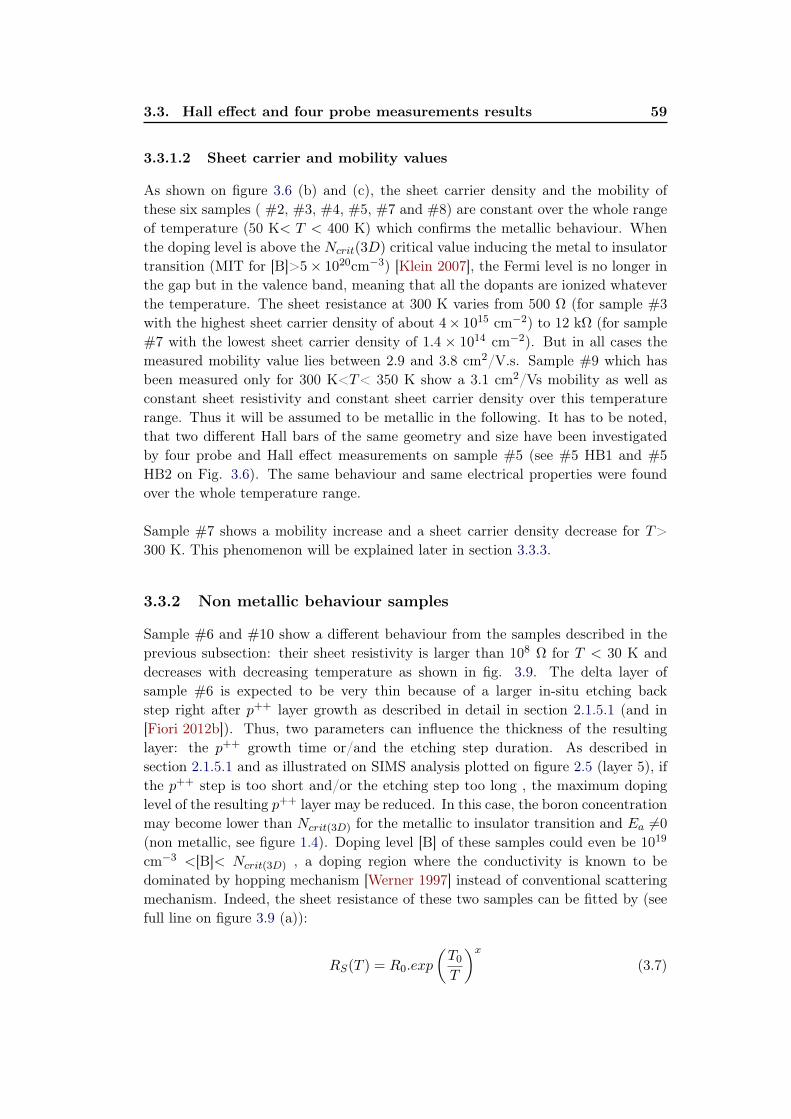
3.3. Hall effect and four probe measurements results 59
3.3.1.2 Sheet carrier and mobility values
As shown on figure 3.6 (b) and (c), the sheet carrier density and the mobility of
these six samples ( #2, #3, #4, #5, #7 and #8) are constant over the whole range
of temperature (50 K< T < 400 K) which confirms the metallic behaviour. When
the doping level is above the Ncrit(3D) critical value inducing the metal to insulator
transition (MIT for [B]>5 1020cm−3) [Klein 2007], the Fermi level is no longer in
the gap but in the valence band, meaning that all the dopants are ionized whatever
the temperature. The sheet resistance at 300 K varies from 500 Ω (for sample #3
with the highest sheet carrier density of about 4 1015 cm−2) to 12 kΩ (for sample
#7 with the lowest sheet carrier density of 1.4 1014 cm−2). But in all cases the
measured mobility value lies between 2.9 and 3.8 cm2/V.s. Sample #9 which has
been measured only for 300 K<T< 350 K show a 3.1 cm2/Vs mobility as well as
constant sheet resistivity and constant sheet carrier density over this temperature
range. Thus it will be assumed to be metallic in the following. It has to be noted,
that two different Hall bars of the same geometry and size have been investigated
by four probe and Hall effect measurements on sample #5 (see #5 HB1 and #5
HB2 on Fig. 3.6). The same behaviour and same electrical properties were found
over the whole temperature range.
Sample #7 shows a mobility increase and a sheet carrier density decrease for T>
300 K. This phenomenon will be explained later in section 3.3.3.
3.3.2 Non metallic behaviour samples
Sample #6 and #10 show a different behaviour from the samples described in the
previous subsection: their sheet resistivity is larger than 108 Ω for T < 30 K and
decreases with decreasing temperature as shown in fig. 3.9. The delta layer of
sample #6 is expected to be very thin because of a larger in-situ etching back
step right after p++ layer growth as described in detail in section 2.1.5.1 (and in
[Fiori 2012b]). Thus, two parameters can influence the thickness of the resulting
layer: the p++ growth time or/and the etching step duration. As described in
section 2.1.5.1 and as illustrated on SIMS analysis plotted on figure 2.5 (layer 5), if
the p++ step is too short and/or the etching step too long , the maximum doping
level of the resulting p++ layer may be reduced. In this case, the boron concentration
may become lower than Ncrit(3D) for the metallic to insulator transition and Ea 6=0
(non metallic, see figure 1.4). Doping level [B] of these samples could even be 1019
cm−3 <[B]< Ncrit(3D) , a doping region where the conductivity is known to be
dominated by hopping mechanism [Werner 1997] instead of conventional scattering
mechanism. Indeed, the sheet resistance of these two samples can be fitted by (see
full line on figure 3.9 (a)):
RS(T ) = R0.exp
T0
T
x
(3.7)
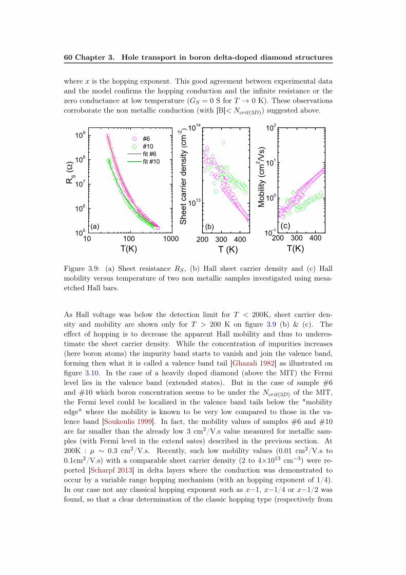
60 Chapter 3. Hole transport in boron delta-doped diamond structures
where x is the hopping exponent. This good agreement between experimental data
and the model confirms the hopping conduction and the infinite resistance or the
zero conductance at low temperature (GS = 0 S for T ! 0 K). These observations
corroborate the non metallic conduction (with [B]< Ncrit(3D)) suggested above.
200 300 40010
-1
100
101
102
Mo
bili
ty (
cm
2/V
s)
T(K)200 300 400
1013
1014
(a) (b)
Sh
ee
t ca
rrie
r d
en
sity (cm
-2)
T (K)
10 100 100010
5
106
107
108
109
#6
#10
fit #6
fit #10
(c)
RS (Ω
)
T(K)
Figure 3.9: (a) Sheet resistance RS , (b) Hall sheet carrier density and (c) Hall
mobility versus temperature of two non metallic samples investigated using mesa-
etched Hall bars.
As Hall voltage was below the detection limit for T < 200K, sheet carrier den-
sity and mobility are shown only for T > 200 K on figure 3.9 (b) & (c). The
effect of hopping is to decrease the apparent Hall mobility and thus to underes-
timate the sheet carrier density. While the concentration of impurities increases
(here boron atoms) the impurity band starts to vanish and join the valence band,
forming then what it is called a valence band tail [Ghazali 1982] as illustrated on
figure 3.10. In the case of a heavily doped diamond (above the MIT) the Fermi
level lies in the valence band (extended states). But in the case of sample #6
and #10 which boron concentration seems to be under the Ncrit(3D) of the MIT,
the Fermi level could be localized in the valence band tails below the "mobility
edge" where the mobility is known to be very low compared to those in the va-
lence band [Soukoulis 1999]. In fact, the mobility values of samples #6 and #10
are far smaller than the already low 3 cm2/V.s value measured for metallic sam-
ples (with Fermi level in the extend sates) described in the previous section. At
200K : µ 0.3 cm2/V.s. Recently, such low mobility values (0.01 cm2/V.s to
0.1cm2/V.s) with a comparable sheet carrier density (2 to 41013 cm−3) were re-
ported [Scharpf 2013] in delta layers where the conduction was demonstrated to
occur by a variable range hopping mechanism (with an hopping exponent of 1/4).
In our case not any classical hopping exponent such as x=1, x=1/4 or x=1/2 was
found, so that a clear determination of the classic hopping type (respectively from

3.3. Hall effect and four probe measurements results 61
mobility
edge
localized
states
Fermi energy
Extended
states
density of
states
Figure 3.10: The concept of the mo-
bility edge. Electronic states below
and above the mobility edge are local-
ized and extended respectively. If the
Fermi energy lies in the region of the
localized states, the system is insulat-
ing at T=0 K. In the extended states
region, the system is metallic. From
[Kramer 1993].
nearest-neighbour, Mott variable-range and Efros-Shklovskii variable range hopping)
mechanism is possible [Tsukioka 2006]. However, it has been found for sample #6
and #10 an anomalous dependence of RS in temperature with x=0.7 (as shown
on figure 3.11). Such hopping exponent of 0.7 has already been observed in thin
metallic films [van der Putten 1992, Van Keuls 1997, Adkins 1998, Marković 2000]
but have been rarely discussed. According to [Shklovskii 2008], it may be a partic-
ular case of variable range hopping in case of a 2D metallic layer (high dielectric
constant) embedded between insulating layer (low dielectric constant). In our case,
it has to be noticed that this hopping mechanism with x=0.7 has been observed in
two samples grown in different type of reactors by using two different techniques in
two different laboratories. Thus, it must be linked to the delta-structure architec-
ture itself. The fit using Eq. 3.7 plotted on figure 3.9 gives T0=780 K and T0=540
K for #6 and #10 respectively.
0,000 0,025 0,050 0,075
105
106
107
108
#6
#10
(90K)
Rs(!
)
1/T0.7
(1/K0.7
)
(40K)
3 4 5 6
-6
-5
-4
-3
-2
-1
ln(d
ln(G
s)/
dT
)
ln(T)
x=0.7 Figure 3.11: Sheet resis-
tance versus 1/T x plot of
two non metallic samples
#6 and #9. The hopping
exponent x = 0.7 was
determined from the slope
of ln(dln(σ)/dT ) versus
ln(T ) plotted in the inset.
3.3.3 Multiple conduction paths
In addition to metallic and non metallic conduction previously described a two
regime conduction is observed in sample #1: in the lowest temperature range (6 K

62 Chapter 3. Hole transport in boron delta-doped diamond structures
< T < 150 K), a metallic conduction characterized by constant values of the mobility
and the sheet carrier density, and then, above 150 K, an increase of the mobility and
a decrease of the sheet carrier density versus temperature. In a delta structure, there
Diamond(substrate(
Buffer(layer((NiD)(
Cap(layer((NiD)(
1016
1017
1018
1019
1020
1021
[B](cm-3)
Depth
(nm
)
#1
0 2
00 4
00 6
00 8
00 1
000
13 nm/dec
9 nm/dec
Figure 3.12: Schematic of the layers stack and secondary ion mass spectroscopy
(SIMS) analysis of sample #1. In between an illustration of the different current
paths through the structure is proposed. The black arrow on SIMS analysis marks
the interface between buffer layer and substrate. The doping tail width value of the
edge sharpnesses are also given on the SIMS profile even if they are probably over-
estimated due to ion mixing and to an insufficient sampling. For the same reason,
the maximum doping of the delta-layer is probably under estimated.
is not only a single path for the current. Indeed, even if the more obvious path is the
delta layer thanks to its low conductivity, current could also flow through the edge of
the delta layer (gradient of doping between NiD region doped at 1016 cm−3 and the
maximum doping level of the delta layer) or even through the NiD region (buffer
and cap layer). Such possibilities are illustrated on figure 3.12 where the sample
can be considered as several resistances (of different values) in parallel. Therefore,
in this part, we will determinate which part of the delta structure contribute to
the multiple conduction using a multi layer Hall effect model recently detailed in
[Look 2008]. This multi layer Hall effect model with arbitrary surface dopant profiles
[Look 2008] has been used here to investigate important characteristics of the delta-
doped structure: i) the influence of the sharpness of the boron acceptor profile and
ii) the influence of the buffer layer on the total hole conduction of the structure
(conductivity, mobility and sheet density).
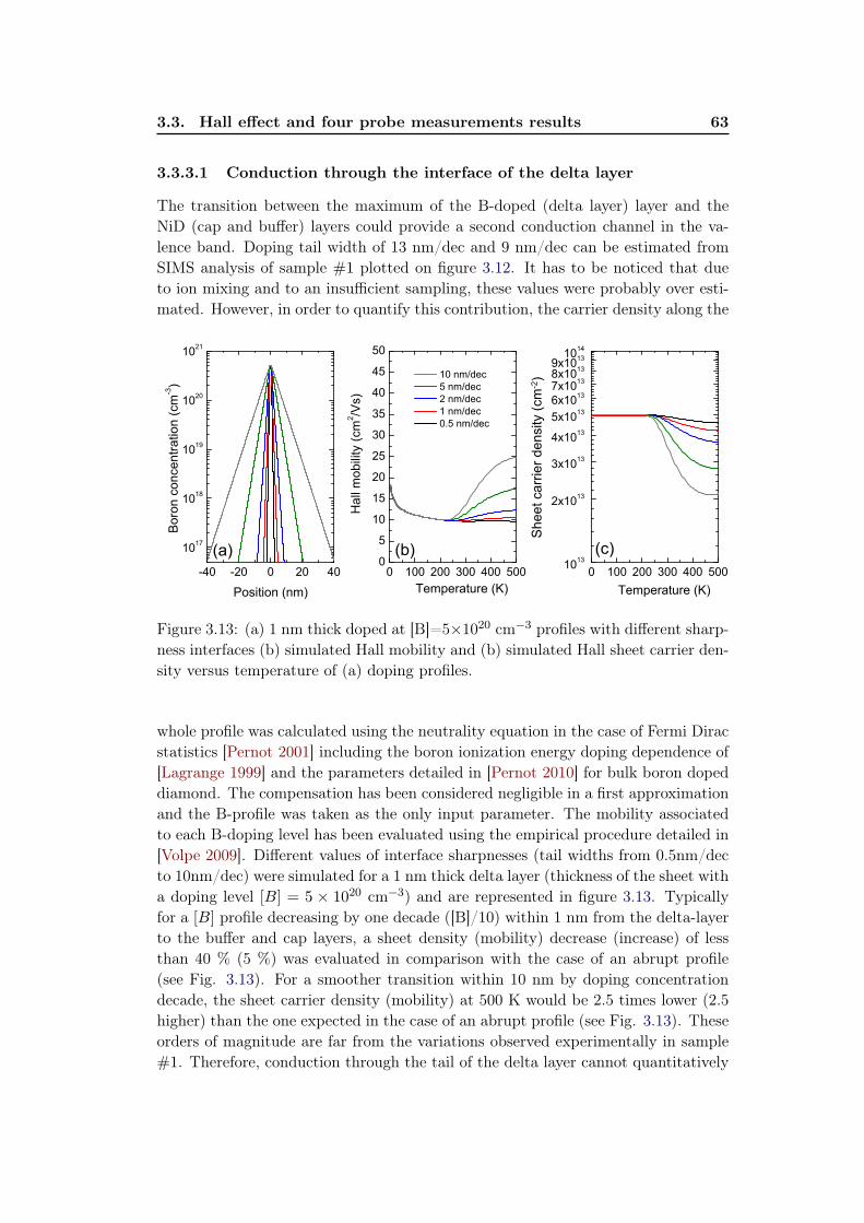
3.3. Hall effect and four probe measurements results 63
3.3.3.1 Conduction through the interface of the delta layer
The transition between the maximum of the B-doped (delta layer) layer and the
NiD (cap and buffer) layers could provide a second conduction channel in the va-
lence band. Doping tail width of 13 nm/dec and 9 nm/dec can be estimated from
SIMS analysis of sample #1 plotted on figure 3.12. It has to be noticed that due
to ion mixing and to an insufficient sampling, these values were probably over esti-
mated. However, in order to quantify this contribution, the carrier density along the
-40 -20 0 20 40
1017
1018
1019
1020
1021
0 100 200 300 400 50010
13
2x10¹³
3x10¹³
4x10¹³
5x10¹³
6x10¹³
7x10¹³
8x10¹³
9x10¹³
1014
0 100 200 300 400 5000
5
10
15
20
25
30
35
40
45
50
Bo
ron
co
nce
ntr
atio
n (
cm
-3)
Position (nm)
(a) (b)
Sh
ee
t ca
rrie
r d
en
sity (
cm
-2)
Temperature (K)
(c)
Temperature (K)
10 nm/dec
5 nm/dec
2 nm/dec
1 nm/dec
0.5 nm/dec
Ha
ll m
ob
ility
(cm
2/V
s)
Figure 3.13: (a) 1 nm thick doped at [B]=51020 cm−3 profiles with different sharp-
ness interfaces (b) simulated Hall mobility and (b) simulated Hall sheet carrier den-
sity versus temperature of (a) doping profiles.
whole profile was calculated using the neutrality equation in the case of Fermi Dirac
statistics [Pernot 2001] including the boron ionization energy doping dependence of
[Lagrange 1999] and the parameters detailed in [Pernot 2010] for bulk boron doped
diamond. The compensation has been considered negligible in a first approximation
and the B-profile was taken as the only input parameter. The mobility associated
to each B-doping level has been evaluated using the empirical procedure detailed in
[Volpe 2009]. Different values of interface sharpnesses (tail widths from 0.5nm/dec
to 10nm/dec) were simulated for a 1 nm thick delta layer (thickness of the sheet with
a doping level [B] = 5 1020 cm−3) and are represented in figure 3.13. Typically
for a [B] profile decreasing by one decade ([B]/10) within 1 nm from the delta-layer
to the buffer and cap layers, a sheet density (mobility) decrease (increase) of less
than 40 % (5 %) was evaluated in comparison with the case of an abrupt profile
(see Fig. 3.13). For a smoother transition within 10 nm by doping concentration
decade, the sheet carrier density (mobility) at 500 K would be 2.5 times lower (2.5
higher) than the one expected in the case of an abrupt profile (see Fig. 3.13). These
orders of magnitude are far from the variations observed experimentally in sample
#1. Therefore, conduction through the tail of the delta layer cannot quantitatively

64 Chapter 3. Hole transport in boron delta-doped diamond structures
describe the phenomenon observed experimentally.
3.3.3.2 Conduction through the NiD parts of the delta-structure
The second possibility investigated here is the hole conduction through the buffer
layer. Its boron concentration is 31016 cm−3 (measured by SIMS, figure 3.12)
homogeneously distributed throughout the active 850 nm of the buffer layer (this
active thickness takes into account the 200 insulating nanometers related to the ex-
tension of the space charge region in the B-doped layer resulting from the nitrogen
n-type doping of the Ib-type substrate, see section 2.2.4.1). With theses values and
assuming a typical compensation [Volpe 2009] of 1015 cm−3, we calculate the mo-
bility, the sheet density and the conductivity temperature dependence of the buffer
layer (dashed lines on Figs 3.14 (b) & (c)). Then, using a T-independent mobility
and sheet carrier concentration for the metallic delta-doped region (dotted lines on
Figs 3.14, µH = 1.5 cm2/V.s and pS = 4 1014 cm−2), the mixed mobility and
sheet density corresponding to the abrupt junction between these two layers were
calculated (full lines on Figs 3.14).The resulting simulated mobility and sheet carrier
density are plotted on Fig. 3.14. As shown on figures 3.14, calculated values are
0 200 400
104
2x10⁴
3x10⁴
0 200 40010
-1
100
101
102
103
104
(a) (b) (c)
Mo
bili
ty (
cm
2/V
s)
T (K)0 200 400
108
109
1010
1011
1012
1013
1014
1015
#1
simu #1
simu metal
simu buffer
#348
Sh
ee
t ca
rrie
r d
en
sity (cm
-2)
T (K)
RS( Ω
)
T (K)
Figure 3.14: Temperature dependance of (a) sheet resistivity, (b) Hall sheet carrier
density and (c) Hall mobility of sample #1. The dashed lines correspond to the
calculated values in the buffer layer with [B] = 3 1016 cm−3 (SIMS) and compen-
sation equals to 1015 cm−3 distributed over the 850 nm active layer. The dotted
lines are the values assumed for the metallic highly doped region (T -independent
and values measured at 5 K, µH = 1.5 cm2/V.s and pS = 4 1014 cm−2). The full
lines correspond to the two layers Hall mobility and sheet density using a multilayer
Hall effect model. Data from [Balmer 2013] were also added to (b) and (c) plots.
in agreement with the experimental data. The observed temperature dependences
were induced by a mixed conduction in both a thin metallic (highly p−doped) layer
3.3. Hall effect and four probe measurements results 65
and in a buffer (+ cap) NiD layer allowing higher mobilities. At low temperatures,
the metallic layer (δ layer) controls completely the apparent mobility and sheet den-
sity but as the temperature is increased, the dopants of the thick buffer (850 nm)
become ionized and the buffer layer begins to contribute to the total conduction of
the structure. Consequently, the delta layer cannot be considered alone to describe
the experimental data of the structure in the high temperature range T >150 K. The
carriers responsible of the conduction at high temperature come from the B-dopants
in the buffer and are not due to a delocalisation of the carrier from the delta-layer.
Similar results were reported by Balmer et al. [Balmer 2013] and are plotted on
figure 3.14 (sample #348): very low mobility at low temperature (µH 1 cm2/V.s
at 100 K) and high mobility at room temperature (µH 70 cm2/V.s). They at-
tributed this behaviour to a two carrier-type model was developed with an activation
energy of 0.2 eV between the delta layer lowest subband with mobility 1 cm2/Vs
and the bulk valence band with high mobility. According to them, this high mo-
bility could not be associated with the bulk of the buffer layer since they did not
observe any conduction in mesa isolation structure. However, it has to be noticed
that their delta layer were grown on a 0.5 µm thick buffer (which is expected to be
intrinsic) and that the mobility and sheet carrier density temperature dependence
are very similar to the one observed in sample #1 (cf. figure 3.14). Thus, from our
understanding, the buffer conduction hypothesis could not be discarded.
To summarize this part, the mobility and sheet density measured by Hall effect
at room temperature are not related to the delta layer in the case of a thick buffer
layer. A temperature dependent measurement is needed in order to identify the con-
tribution of each layer of the delta doped structure to the total conduction, and so
to the apparent mobility. A way to avoid this problem is to grow a sufficiently thin
buffer layer (active layer thinner than 100 nm for a 2 nm thick delta doped layer).
In fact, as mentioned above and detailed in the previous chapter (section 2.2.4.1),
Ib-type substrates (mainly used in this work) contain nitrogen at concentration of
few 1019 cm−3. In that cases, the main part of the buffer (at least 200 nm: see Fig.
2.12) is inactive due to the extension of the space charge region of the pn junction
formed by the p-type B-doped buffer and the n-type N-doped diamond substrate.
That is why, a thickness value of about 300 nm was chosen for the buffer layer of all
samples of this work (except sample #1). As can be observed on the temperature
dependence of the electrical properties, none of the samples grown after sample #1
shows a double conduction behaviour, except sample #7. Indeed, below room tem-
perature the conduction observed is typical of a metal like diamond (constant pSand µH) but for T > 300 K the mobility begins to increase slowly. This phenomenon
could be explained by a parallel conduction through the buffer and the cap layer
(i.e. nid regions) at high temperature when the NiD layers begins to be thermally
ionized and to participate to the conduction as it has been described for sample
#1. This conduction of the buffer is only observed in this sample even though the
buffer layers of other samples are as thick (or thicker) as the one of sample #7 (see
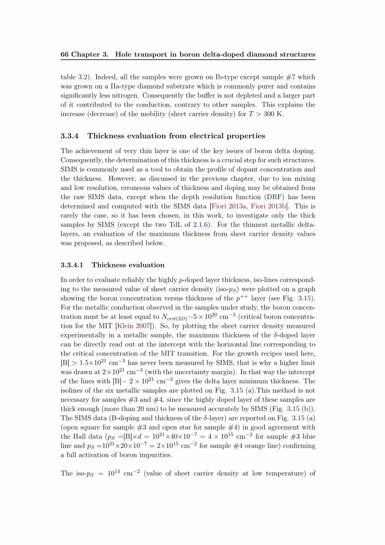
66 Chapter 3. Hole transport in boron delta-doped diamond structures
table 3.2). Indeed, all the samples were grown on Ib-type except sample #7 which
was grown on a IIa-type diamond substrate which is commonly purer and contains
significantly less nitrogen. Consequently the buffer is not depleted and a larger part
of it contributed to the conduction, contrary to other samples. This explains the
increase (decrease) of the mobility (sheet carrier density) for T > 300 K.
3.3.4 Thickness evaluation from electrical properties
The achievement of very thin layer is one of the key issues of boron delta doping.
Consequently, the determination of this thickness is a crucial step for such structures.
SIMS is commonly used as a tool to obtain the profile of dopant concentration and
the thickness. However, as discussed in the previous chapter, due to ion mixing
and low resolution, erroneous values of thickness and doping may be obtained from
the raw SIMS data, except when the depth resolution function (DRF) has been
determined and computed with the SIMS data [Fiori 2013a, Fiori 2013b]. This is
rarely the case, so it has been chosen, in this work, to investigate only the thick
samples by SIMS (except the two TdL of 2.1.6). For the thinnest metallic delta-
layers, an evaluation of the maximum thickness from sheet carrier density values
was proposed, as described below.
3.3.4.1 Thickness evaluation
In order to evaluate reliably the highly p-doped layer thickness, iso-lines correspond-
ing to the measured value of sheet carrier density (iso-pS) were plotted on a graph
showing the boron concentration versus thickness of the p++ layer (see Fig. 3.15).
For the metallic conduction observed in the samples under study, the boron concen-
tration must be at least equal to Ncrit(3D)=5 1020 cm−3 (critical boron concentra-
tion for the MIT [Klein 2007]). So, by plotting the sheet carrier density measured
experimentally in a metallic sample, the maximum thickness of the δ-doped layer
can be directly read out at the intercept with the horizontal line corresponding to
the critical concentration of the MIT transition. For the growth recipes used here,
[B] > 1.51021 cm−3 has never been measured by SIMS, that is why a higher limit
was drawn at 21021 cm−3 (with the uncertainty margin). In that way the intercept
of the lines with [B]= 2 1021 cm−3 gives the delta layer minimum thickness. The
isolines of the six metallic samples are plotted on Fig. 3.15 (a).This method is not
necessary for samples #3 and #4, since the highly doped layer of these samples are
thick enough (more than 20 nm) to be measured accurately by SIMS (Fig. 3.15 (b)).
The SIMS data (B-doping and thickness of the δ-layer) are reported on Fig. 3.15 (a)
(open square for sample #3 and open star for sample #4) in good agreement with
the Hall data (pS =[B]d = 10214010−7 = 4 1015 cm−2 for sample #3 blue
line and pS =10212010−7 = 21015 cm−2 for sample #4 orange line) confirming
a full activation of boron impurities.
The iso-pS = 1014 cm−2 (value of sheet carrier density at low temperature) of

3.3. Hall effect and four probe measurements results 67
samples #2, #7 and #8 indicates that the thickness of the heavily p−doped layer
is found to be equal to or thinner than 2 nm. For such small thickness val-
ues, layer could be considered as two dimensional ones if we used the criteria
of the step-like density of state (see figure 3.3). Thus, one must be aware that
this 2 nm thickness value was determined under the assumption that the boron
ionization energy Ea decreased following the same trend than in 3D case (i.e.
Ea = Ea0(1− ([B]/Ncrit(3D))1/3), see section 3.1.2.2) as plotted on figure 1.4. How-
ever, considering that the 3D properties applied to our case, the deduced thickness
are ever low (<2 nm for the thinnest) which indicates that it is a good assumption.
Indeed, considering Ncrit(2D) > Ncrit(3D) would induce even lower value of thickness
(for instance lower than one single atomic layer) and so, unrealistic value for the
sample with the lowest pS .
0.1 1 10 10010
20
1021
1022
#2#7
#8 #5 #1 #4 #3
pS =
2x10 15 cm
-2
pS =
4x10 14 cm
-2
pS =
10 14 cm
-2
[B]
(cm
-3)
Thickness (nm)
pS =
4x10 15 cm
-2
MIT
0 50 100 150 200 25010
16
1017
1018
1019
1020
1021
#3
#4
(a) (b)
[B]
(cm
-3)
Depth (nm)
Figure 3.15: (a) Iso-sheet carrier density lines measured by Hall effect plotted on a
boron concentration (cm−3) versus thickness (nm) plot. For [B] ≥ 5 1020 cm−3,
the conduction is metallic. For the growth recipes used to grow delta layer, [B] >
1.5 1021 cm−3 has never been measured by SIMS, that is why an high limit was
drawn at 2 1021 cm−3. The intercept of the lines (boundaries between full and
dashed) with the horizontal line corresponding to the critical concentration for the
metal-insulator transition (MIT) yield the maximum thickness of the highly doped
region where [B] > 51020 cm−3 while the intercept of the lines with [B]= 21021
cm−3 gives the minimum thickness. The symbols are SIMS data for samples #3
(square) and sample #4 (star). (b) SIMS analysis of the two thickest samples of
this work (#3 and #4).
3.3.4.2 Comparison with physico-chemical analysis results
Samples #2, #7 and #8 are the thinnest metallic layers of this work. A structure
grown with exactly the same process than samples #7 and #8 exhibited a thickness

68 Chapter 3. Hole transport in boron delta-doped diamond structures
of 1.3 nm when measured by ellipsometry [Bousquet 2014]. Furthermore, the p++
layers of these 2 samples were grown in the same conditions than the ones of the
2 multi-layers analyzed by TEM and SIMS (see chapter 2), except for the etching
step durations. Delta ↵ (2 nm from HAADF), delta β (3 nm) and the 2 delta layers
of #7 and #8 were etched respectively during 7 min, 6 min and 5 min in the H2/O2
mixture, plus 6 min in pure H2. This seems to be in relatively good agreement with
the thickness determined by SIMS and from electrical properties. For other thin
samples (#5, #7, #8), the correlation between etching duration steps and thick-
ness was not obvious. In fact, as nanometric scale are reached, with a delta layer
thickness in the same order as the roughness of sample surfaces, the control of the
thickness and of the doping peaks value [Fiori 2012b] become a very tough techno-
logical challenge. Nevertheless the thickness of delta layer of sample #5 deduced
from its sheet carrier density (5 nm if doped at 5 1020 cm−3 or 2.5 nm if doped at
1 1021 cm−3 as shown on figure 3.15) is in good agreement with the 3.3 nm value
determined by ellipsometry measurements [Bousquet 2014].
As explained above, an in situ etching technique was used to reduce the thickness
of the delta layer. Different etching times were tried out to reduce the thickness,
but not any metallic delta layer with pS < 1014 cm−2 was obtained and the layers
which could be thinner (samples #6 and #10) were not metallic.
3.4 Discussion of mobility
A mobility value of 3 ±1 cm2/V.s was measured for the seven metallic samples
of this work, whatever their thicknesses. Two questions arise:
• Why are the mobility values of all these samples the same ?
• Why is this mobility value ( 3 ±1 cm2/V.s) so low ?
In this section, we will explore the possible mechanisms that can limit the mobility
to this value of 3 ±1 cm2/V.s by using two dimensional and three dimensional
approaches.
3.4.1 2D gas mobility model
As already discussed, and taking into account the delta layers nano-metric size that
have been reached in this work, it is legitimate to consider the thinnest delta layers
as 2D systems (samples #2, #5,#7,#8). Therefore, in this case the mobility model
that have been developed for two dimensional gas will be used. Mobility limitations
by acoustic phonon scattering and ionized impurities scattering will be considered
in the following. Optical phonon scattering mechanisms was assumed to affect the
mobility at higher temperatures than those of interest in this work.
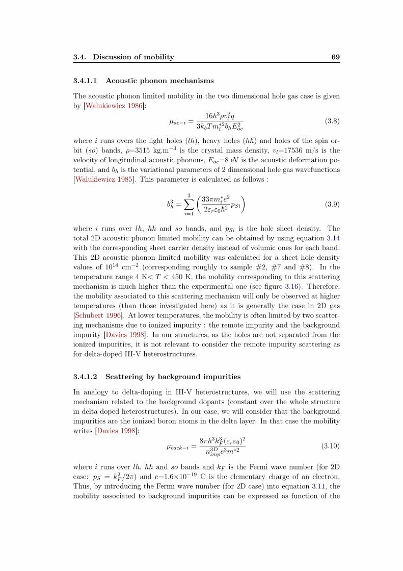
3.4. Discussion of mobility 69
3.4.1.1 Acoustic phonon mechanisms
The acoustic phonon limited mobility in the two dimensional hole gas case is given
by [Walukiewicz 1986]:
µac−i =16~3v2l q
3kbTm2i bhE2
ac
(3.8)
where i runs overs the light holes (lh), heavy holes (hh) and holes of the spin or-
bit (so) bands, =3515 kg.m−3 is the crystal mass density, vl=17536 m/s is the
velocity of longitudinal acoustic phonons, Eac=8 eV is the acoustic deformation po-
tential, and bh is the variational parameters of 2 dimensional hole gas wavefunctions
[Walukiewicz 1985]. This parameter is calculated as follows :
b3h =
3X
i=1
33m
i e2
2"r"0~2pSi
(3.9)
where i runs over lh, hh and so bands, and pSi is the hole sheet density. The
total 2D acoustic phonon limited mobility can be obtained by using equation 3.14
with the corresponding sheet carrier density instead of volumic ones for each band.
This 2D acoustic phonon limited mobility was calculated for a sheet hole density
values of 1014 cm−2 (corresponding roughly to sample #2, #7 and #8). In the
temperature range 4 K< T < 450 K, the mobility corresponding to this scattering
mechanism is much higher than the experimental one (see figure 3.16). Therefore,
the mobility associated to this scattering mechanism will only be observed at higher
temperatures (than those investigated here) as it is generally the case in 2D gas
[Schubert 1996]. At lower temperatures, the mobility is often limited by two scatter-
ing mechanisms due to ionized impurity : the remote impurity and the background
impurity [Davies 1998]. In our structures, as the holes are not separated from the
ionized impurities, it is not relevant to consider the remote impurity scattering as
for delta-doped III-V heterostructures.
3.4.1.2 Scattering by background impurities
In analogy to delta-doping in III-V heterostructures, we will use the scattering
mechanism related to the background dopants (constant over the whole structure
in delta doped heterostructures). In our case, we will consider that the background
impurities are the ionized boron atoms in the delta layer. In that case the mobility
writes [Davies 1998]:
µback−i =8~3k3F ("r"0)
2
n3Dimpe
3m2(3.10)
where i runs over lh, hh and so bands and kF is the Fermi wave number (for 2D
case: pS = k2F /2) and e=1.610−19 C is the elementary charge of an electron.
Thus, by introducing the Fermi wave number (for 2D case) into equation 3.11, the
mobility associated to background impurities can be expressed as function of the

70 Chapter 3. Hole transport in boron delta-doped diamond structures
sheet hole density pSi of each band:
µback−i =8~3(2pSi)
3/2("r"0)2
n3Dimpe
3m2(3.11)
In our case, the most of the of holes lie in the quantum well formed by the delta
layer. Thus the impurity density to consider is the one of the delta layer. That is
why a value of 1021 cm−3 (which is the typical boron concentration expected for
the growth process used) will be taken for n3Dimp. For the sheet carrier density, a
total value of 1014 cm−2 was considered. Then, the background impurity can be
calculated for each band and the total corresponding mobility is obtained using Eq.
3.14 with the corresponding sheet carrier density instead of volumic ones for each
band. A mobility value µback = 3.3 cm2/V.s is found. As shown on figure 3.16,
Figure 3.16: Temperature de-
pendance of the experimental
mobility of metallic samples and
of theoretical calculated acoustic
phonons mobility and background
impurities mobility. Theoretical
mobilities were calculated with 2D
models for a 2D layer with pS=1014
cm−3.
10 10010
0
101
102
103
104
105
µback (p
s=10
14 cm
-2)
#7
#8
#9
#2
#3
#4
#5 HB1
#5 HB2
Mo
bili
ty (
cm
2/V
s)
T(K)
µac-2D
(ps=10 14
cm -2)
this calculated value is in good agreement with the experimental mobility values
measured over the whole temperature range. Nevertheless, it is relevant only for
samples #2, #7 and #8 for which the sheet carrier density is nearly the one used
in the calculation.
The mobility associated to the scattering by background impurities calculated for a
2D holes gas with pS=1014 cm−2 is also in good agreement with others samples where
larger different sheet carrier density values where measured: from pS=3.21014
cm−2 (sample #5) to pS=4.41015 cm−2 (sample #3). Therefore, as shown on the
plot of mobility versus sheet carrier density of figure 3.17, the background impu-
rity scattering mechanism could not explain the same mobility value measured in
metallic samples #3, #4, #5 and #9 showing larger sheet carrier density.
3.4.1.3 Other scattering mechanisms in 2D gas
It is commonly admitted that other scattering mechanisms can occur in 2D gas.
Interface roughness and imperfections can be responsible of deviation from the per-
fect crystal and so create scattering. For instance, dislocations has already been
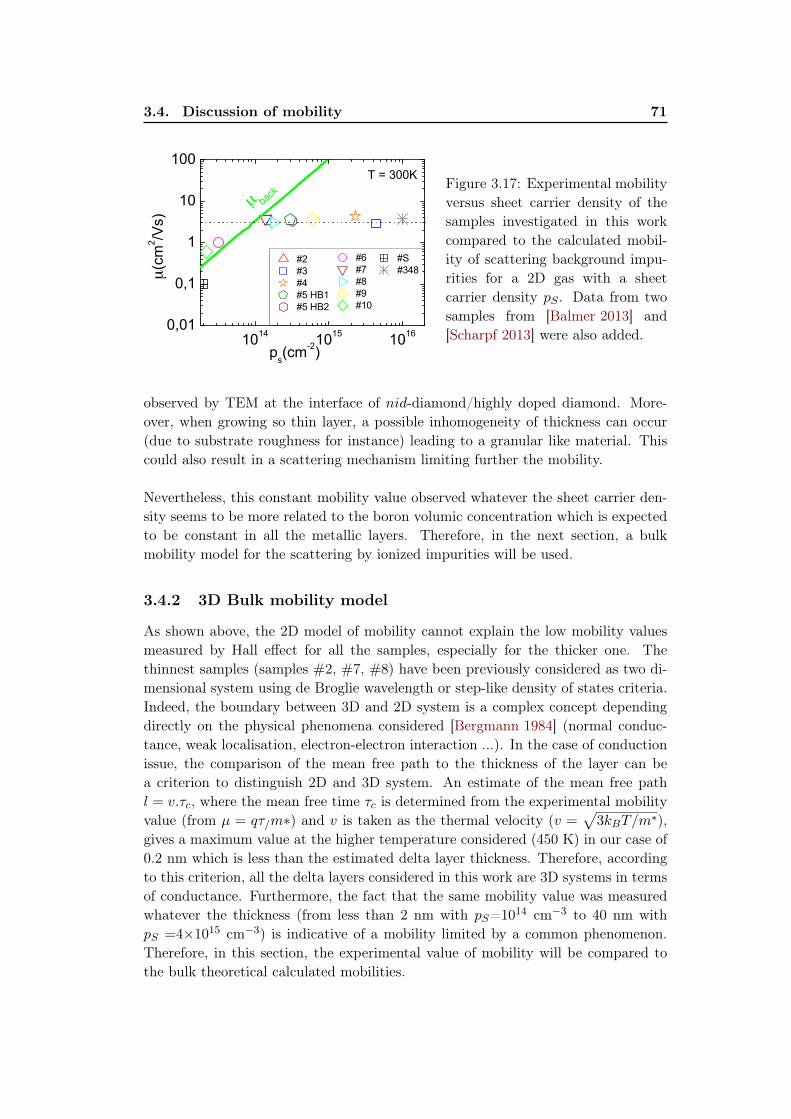
3.4. Discussion of mobility 71
1014
1015
1016
0,01
0,1
1
10
100
#6
#7
#8
#9
#10
#2
#3
#4
#5 HB1
#5 HB2
#S
#348
µ back
µ(c
m2/V
s)
ps(cm
-2)
T = 300KFigure 3.17: Experimental mobility
versus sheet carrier density of the
samples investigated in this work
compared to the calculated mobil-
ity of scattering background impu-
rities for a 2D gas with a sheet
carrier density pS . Data from two
samples from [Balmer 2013] and
[Scharpf 2013] were also added.
observed by TEM at the interface of nid-diamond/highly doped diamond. More-
over, when growing so thin layer, a possible inhomogeneity of thickness can occur
(due to substrate roughness for instance) leading to a granular like material. This
could also result in a scattering mechanism limiting further the mobility.
Nevertheless, this constant mobility value observed whatever the sheet carrier den-
sity seems to be more related to the boron volumic concentration which is expected
to be constant in all the metallic layers. Therefore, in the next section, a bulk
mobility model for the scattering by ionized impurities will be used.
3.4.2 3D Bulk mobility model
As shown above, the 2D model of mobility cannot explain the low mobility values
measured by Hall effect for all the samples, especially for the thicker one. The
thinnest samples (samples #2, #7, #8) have been previously considered as two di-
mensional system using de Broglie wavelength or step-like density of states criteria.
Indeed, the boundary between 3D and 2D system is a complex concept depending
directly on the physical phenomena considered [Bergmann 1984] (normal conduc-
tance, weak localisation, electron-electron interaction ...). In the case of conduction
issue, the comparison of the mean free path to the thickness of the layer can be
a criterion to distinguish 2D and 3D system. An estimate of the mean free path
l = v.c, where the mean free time c is determined from the experimental mobility
value (from µ = q/m) and v is taken as the thermal velocity (v =p
3kBT/m),
gives a maximum value at the higher temperature considered (450 K) in our case of
0.2 nm which is less than the estimated delta layer thickness. Therefore, according
to this criterion, all the delta layers considered in this work are 3D systems in terms
of conductance. Furthermore, the fact that the same mobility value was measured
whatever the thickness (from less than 2 nm with pS=1014 cm−3 to 40 nm with
pS =41015 cm−3) is indicative of a mobility limited by a common phenomenon.
Therefore, in this section, the experimental value of mobility will be compared to
the bulk theoretical calculated mobilities.
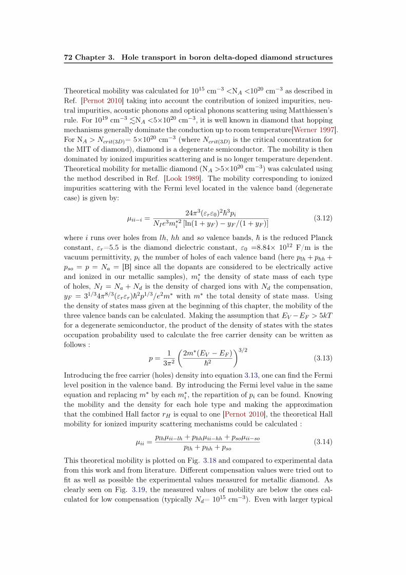
72 Chapter 3. Hole transport in boron delta-doped diamond structures
Theoretical mobility was calculated for 1015 cm−3 <NA <1020 cm−3 as described in
Ref. [Pernot 2010] taking into account the contribution of ionized impurities, neu-
tral impurities, acoustic phonons and optical phonons scattering using Matthiessen’s
rule. For 1019 cm−3 .NA <51020 cm−3, it is well known in diamond that hopping
mechanisms generally dominate the conduction up to room temperature[Werner 1997].
For NA > Ncrit(3D)= 51020 cm−3 (where Ncrit(3D) is the critical concentration for
the MIT of diamond), diamond is a degenerate semiconductor. The mobility is then
dominated by ionized impurities scattering and is no longer temperature dependent.
Theoretical mobility for metallic diamond (NA >51020 cm−3) was calculated using
the method described in Ref. [Look 1989]. The mobility corresponding to ionized
impurities scattering with the Fermi level located in the valence band (degenerate
case) is given by:
µii−i =243("r"0)
2~3pi
NIe3m2i [ln(1 + yF )− yF /(1 + yF )]
(3.12)
where i runs over holes from lh, hh and so valence bands, ~ is the reduced Planck
constant, "r=5.5 is the diamond dielectric constant, "0 =8.84 1012 F/m is the
vacuum permittivity, pi the number of holes of each valence band (here plh + phh +
pso = p = Na = [B] since all the dopants are considered to be electrically active
and ionized in our metallic samples), m
i the density of state mass of each type
of holes, NI = Na + Nd is the density of charged ions with Nd the compensation,
yF = 31/348/3("r"r)~2p1/3/e2m with m the total density of state mass. Using
the density of states mass given at the beginning of this chapter, the mobility of the
three valence bands can be calculated. Making the assumption that EV −EF > 5kT
for a degenerate semiconductor, the product of the density of states with the states
occupation probability used to calculate the free carrier density can be written as
follows :
p =1
32
2m(EV − EF )
~2
3/2
(3.13)
Introducing the free carrier (holes) density into equation 3.13, one can find the Fermi
level position in the valence band. By introducing the Fermi level value in the same
equation and replacing m by each m
i , the repartition of pi can be found. Knowing
the mobility and the density for each hole type and making the approximation
that the combined Hall factor rH is equal to one [Pernot 2010], the theoretical Hall
mobility for ionized impurity scattering mechanisms could be calculated :
µii =plhµii−lh + phhµii−hh + psoµii−so
plh + phh + pso(3.14)
This theoretical mobility is plotted on Fig. 3.18 and compared to experimental data
from this work and from literature. Different compensation values were tried out to
fit as well as possible the experimental values measured for metallic diamond. As
clearly seen on Fig. 3.19, the measured values of mobility are below the ones cal-
culated for low compensation (typically Nd= 1015 cm−3). Even with larger typical

3.4. Discussion of mobility 73
compensation ratios the calculated mobility remained larger than the experimental
values. It has to be noticed that this value of mobility around 3 cm2/V.s was not
only measured in the samples of this work but also in other reports of literature
(see sample #366 of Ref [Balmer 2013] in table 3.2) and then seems to be inherent
to heavily doped diamond (with [B]> Ncrit(3D)). One can think about a possible
solubility limit of boron in diamond, limiting the boron acceptor and leading to a
boron self compensation effect. In fact with a compensation ratio close to unity, the
theoretical mobility shrinks toward experimental measured values. Nevertheless, for
samples #3 and #4 which have been analyzed by SIMS, a complete ionization of
boron atoms has been observed (i.e. p=[B], see figure 3.15) weakening the self com-
pensation hypothesis (at least for these two samples).
1017
1018
1019
1020
1021
1022
0.1
1
10
100
1000
Theoretical mobility (300K)
Werner et al. (1997)
Tsukioka et al. (2006)
Thonke et al. (2003)
Mortet et al. (2008)
Gabrysch et al. (2008) NCD
Klein et al. (2007) 1/Rh
This work
Mobili
ty (
cm
2/V
s)
NA (cm
-3)
300K
Hoppin
g
Figure 3.18: Hole Hall mobility as function of doping level in homoepitaxial dia-
mond of samples from this work and from literature [Thonke 2003, Werner 1997,
Tsukioka 2006, Mortet 2008, Gabrysch 2008, Klein 2007]. The theoretical mobility
is illustrated by the black solid line and was calculated using calculations detailed
in [Pernot 2010] for NA <1020 cm−3 and for NA >51020 cm−3 by equations 3.12
and 3.14.
However, even if these calculations cannot fully describe the value of the mobil-
ity, the most likely limitating scattering mechanism is the one linked to the ionized
impurity. Indeed, if the same boron doping level [B] is achieved in the different
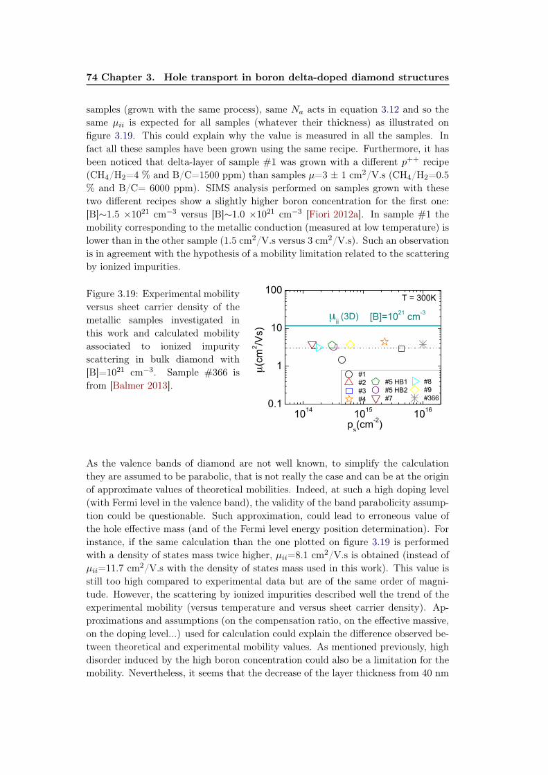
74 Chapter 3. Hole transport in boron delta-doped diamond structures
samples (grown with the same process), same Na acts in equation 3.12 and so the
same µii is expected for all samples (whatever their thickness) as illustrated on
figure 3.19. This could explain why the value is measured in all the samples. In
fact all these samples have been grown using the same recipe. Furthermore, it has
been noticed that delta-layer of sample #1 was grown with a different p++ recipe
(CH4/H2=4 % and B/C=1500 ppm) than samples µ=3 ± 1 cm2/V.s (CH4/H2=0.5
% and B/C= 6000 ppm). SIMS analysis performed on samples grown with these
two different recipes show a slightly higher boron concentration for the first one:
[B]1.5 1021 cm−3 versus [B]1.0 1021 cm−3 [Fiori 2012a]. In sample #1 the
mobility corresponding to the metallic conduction (measured at low temperature) is
lower than in the other sample (1.5 cm2/V.s versus 3 cm2/V.s). Such an observation
is in agreement with the hypothesis of a mobility limitation related to the scattering
by ionized impurities.
Figure 3.19: Experimental mobility
versus sheet carrier density of the
metallic samples investigated in
this work and calculated mobility
associated to ionized impurity
scattering in bulk diamond with
[B]=1021 cm−3. Sample #366 is
from [Balmer 2013].
1014
1015
1016
0.1
1
10
100
[B]=1021
cm-3
#5 HB1
#5 HB2
#7
#8
#9
#366
#1
#2
#3
#4
µii (3D)
µ(c
m2/V
s)
ps(cm
-2)
T = 300K
As the valence bands of diamond are not well known, to simplify the calculation
they are assumed to be parabolic, that is not really the case and can be at the origin
of approximate values of theoretical mobilities. Indeed, at such a high doping level
(with Fermi level in the valence band), the validity of the band parabolicity assump-
tion could be questionable. Such approximation, could lead to erroneous value of
the hole effective mass (and of the Fermi level energy position determination). For
instance, if the same calculation than the one plotted on figure 3.19 is performed
with a density of states mass twice higher, µii=8.1 cm2/V.s is obtained (instead of
µii=11.7 cm2/V.s with the density of states mass used in this work). This value is
still too high compared to experimental data but are of the same order of magni-
tude. However, the scattering by ionized impurities described well the trend of the
experimental mobility (versus temperature and versus sheet carrier density). Ap-
proximations and assumptions (on the compensation ratio, on the effective massive,
on the doping level...) used for calculation could explain the difference observed be-
tween theoretical and experimental mobility values. As mentioned previously, high
disorder induced by the high boron concentration could also be a limitation for the
mobility. Nevertheless, it seems that the decrease of the layer thickness from 40 nm

3.4. Discussion of mobility 75
down to less than 2 nm does not improve the mobility value.
3.4.3 Enhancement of the mobility ?
Calculations based only on the hole distribution in the V-shape potential suggest
that delocalisation would occur for delta layer thickness under 2 nm as it has been
shown at the beginning of the chapter and in [Fiori 2010]. The highly p−doped layer
of samples #2, #7 and #8 are rather thin (< 2 nm), but the mobility measured
is around 3 cm2/V.s which is typically the same than the one measured in thicker
highly p−doped layer like sample #3 (cf. Fig.3.6). The strong coulombic scattering
induced by ionized boron atoms (Fermi screening radius is about 0.3 nm) in the
delta-layer limits the mobility of the free hole in the same proportion than in a
bulk material. No enhancement of the mobility was observed for a delta with pS =
1014 cm−2 corresponding to a maximum thickness of 2 nm. Moreover, no layer
showing metallic behaviour with pS < 1014 cm−2 were obtained in this work. The
possibly thinner layers with lower pS measured in this work or reported in literature
[Scharpf 2013] do not show metallic behaviour and their mobilities are lower than
the metallic one, due to a hopping conduction mechanism between localized gap
states.
76 Chapter 3. Hole transport in boron delta-doped diamond structures
3.5 Conclusion
Hall effect and four probe measurements combined with mesa-structures Hall bars
proved to be very powerful and accurate tools to assess the electrical properties of
delta-layers structure but also to evaluate doping/thickness values for the layer. This
approach becomes necessary for very thin delta layers for which SIMS data could
be erroneous. Nevertheless, to draw the quintessence of these techniques without
obtaining erroneous results, one must analyze them with a great care. For instance,
it has been shown that the analysis of temperature dependence of pS(T) and µH(T)
is useful to distinguish the contribution of each conduction path (buffer/ high B-
doped layer / cap-layer) to the measured (mixed) conductivity. A correct analysis
of the apparent Hall mobility and sheet density is expected to yield the real hole
mobility in the δ-layer or at its interfaces.
Delta structures have been grown on two different types of substrates with 2 differ-
ent types of reactors aiming at obtaining abrupt interfaces, a sufficiently high boron
doping level insuring a metallic conduction in the delta layer and low doped NiD
cap and buffer layers suited for high mobility. Nanometer thick delta layers were
obtained and characterized by SIMS, TEM and Ellipsometry.
Hall effect and four probe investigations confirmed the nanometric thickness and
showed no enhancement of mobility for metallic delta layers thinner than 2 nm,
but a constant mobility value of 3 cm2/V.s was found whatever the thickness of the
delta-layer or the substrate used. Several indications of a scattering mechanisms due
to ionized impurity were pointed out. Because of the low thickness value estimated
from sheet carrier density measurements, it has been firstly though that two dimen-
sional scattering mechanism must be responsible of the low experimental mobility
value measured in metallic delta-layers. Using a model developed for 2D hole gas,
it appeared that the background impurity scattering of carriers (not delocalized out
of the delta) due to the the ionized boron atoms could be an explanation only for
the thinnest layers (with pS 1014cm−3). However, as the same mobility value was
measured for twenty times thicker delta layer, it seems that a mobility bulk model
might be better adapted. The mobility corresponding to ionized impurity scattering
mechanism in bulk diamond with [B]=1021 cm−3 was found to be 4 times higher
than the experimental ones. Approximations and assumptions such as the one con-
sidering the valence band as parabolic could be responsible of this discrepancy.
On the other hand, insulating delta layers exhibited a conduction by hopping mech-
anism with an anomalous exponent of 0.7. Such value have already been reported
in granular thin metallic films but are not yet well understood. Further study on
this mechanism should be undertaken to understand its origin.
To summarize, the thinnest metallic layer was reported with a sheet carrier density
of 1014 cm−2 and a mobility of 3 cm2/V.s. Unfortunately this mobility was too low
to consider that high frequency field effect transistors in diamond using delta-doped
structure could be one day able to compete with the present AlGaN/GaN HEMT

3.5. Conclusion 77
showing mobility of 2200 cm2/V.s. Furthermore, it seems challenging to grow thin-
ner metallic diamond layers and even if achieved, there is no guarantee that such
layers would exhibit a higher mobility than reported in this work. This topic has
been intensively studied over the past few years but none of the recently published
works reported more promising results [Edgington 2012, Balmer 2013, Scharpf 2013]
demonstrating diamond delta-FET with good performances. Therefore other archi-
tectures such as diamond MOSFET have to be investigated.
However, even if the initially target of a delta-field effect transistor seems to not
be promising due to the too low mobility measured in the delta-structures, this
investigation of the delta layer electrical properties allow us to understand and
progress a lot on both diamond growth and electrical characterization techniques.
For instance, the thickness control accuracy during the growth of diamond layers is
already useful for the study of the dimensionality effect of superconducting diamond
in the framework of Jessica Bousquet’s PhD project.
One of the important results of this work was to highlight a mobility value close
to 3 cm2/Vs, whatever the thickness of the B-doped layer (for layer thickness lower
than 40 nm). The model used in this work gives a relative agreement with this
value even if a discrepancy remains. Future works are needed to fully understand
this value. An exact calculation will certainly need a better knowledge of the valence
bands (dispersion and/or boundary with localized states) at energy level close to
the Fermi level of such metallic B-doped diamond.

Chapter 4
Metal Oxide Semiconductor
structure using oxygen-terminated
diamond
Contents
4.1 MOS concept and theory . . . . . . . . . . . . . . . . . . . . 81
4.1.1 Metal insulator semiconductor regimes . . . . . . . . . . . . . 81
4.1.2 QΨ graph : charges vs surface potential . . . . . . . . . . . . 83
4.1.3 MOS C(V ) characteristics . . . . . . . . . . . . . . . . . . . . 87
4.2 MOS characterization techniques . . . . . . . . . . . . . . . . 91
4.2.1 C(V ) measurement principle . . . . . . . . . . . . . . . . . . 91
4.2.2 Impedance model . . . . . . . . . . . . . . . . . . . . . . . . . 92
4.2.3 Experimental setup . . . . . . . . . . . . . . . . . . . . . . . . 96
4.3 MOS fabrication using diamond semiconductor . . . . . . . 96
4.3.1 Low temperature ALD on oxygenated diamond surface . . . . 97
4.3.2 MOS capacitor design . . . . . . . . . . . . . . . . . . . . . . 99
4.3.3 Samples growth and fabrication details . . . . . . . . . . . . . 100
4.4 MOS operating regimes . . . . . . . . . . . . . . . . . . . . . 103
4.4.1 Oxide characterization using MIM structure : sample #0 . . 103
4.4.2 First MOS capacitors: samples #1 and #2 . . . . . . . . . . 104
4.4.3 Diamond layer improvement: samples #3 and #4 . . . . . . 107
4.4.4 Band diagram and leakage current . . . . . . . . . . . . . . . 111
4.4.5 Interface state investigation . . . . . . . . . . . . . . . . . . . 114
4.4.6 Oxide improvement: sample #6 . . . . . . . . . . . . . . . . . 116
4.5 Conclusion and outlook for diamond MOSFET . . . . . . . 121
The conducting or insulating behavior of a metal-oxide-semiconductor field effect
transistor (MOSFET) is based on the electrostatic control of the band curvature at
the oxide/semiconductor interface. In theory, this effect should allow to overcome
the high ionization energy of diamond dopants in the channel. Carriers would then
flow with a high mobility in the channel, opening the way for fast switching MOS-
FET able to withstand high voltage and to get rid efficiently of the heat, thanks

80 Chapter 4. Diamond MOS structure
to diamond material. However, the main problem to fabricate a metal oxide semi-
conductor (MOS) structure is to achieve a sufficiently clean semiconductor oxide
interface in order to control the different regimes of the MOS: accumulation of ma-
jority carriers, depletion, deep depletion or inversion of carriers. This oxide/diamond
interface is highly related to both the oxide and the diamond surface quality. Thus,
the choice of the oxide as well as the diamond surface treatment are of the uttermost
importance. To address this challenge, taking account of the commonly reported
values in literature, we decided to select aluminum oxide deposited by atomic layer
deposition (ALD) on an oxygenated diamond surface because of the expected match
of the oxide with the diamond band gap as shown on figure 4.1 for a low doped dia-
mond. Moreover, the reaction leading to aluminum oxide ALD is known to be well
initialized on hydroxyl (-O-H) terminated surfaces such as the oxygen terminated
diamond one.
Figure 4.1: Theoretical band di-
agram of a MOS structure com-
posed of a stack of Al/Al2O3/p-
type diamond before Fermi level
alignment. Values reported
in literature were taken for
the electronic affinity of oxy-
gen terminated diamond (1.7 eV
[Maier 2001]) and for the band
gap of aluminum oxide deposited
by atomic layer deposition (6.7
eV for deposition at low tempera-
ture [Huang 2009, Nohira 2002]).
qϕm= 3.9 eV
2.9 eV
qΧi =1.0 eV
Egi = 6.7 eV Eg = 5.5 eV
qΧ = 1.7 eV
NV
E
E
EF
Al Al2O3 p-type diamond
C
V
The first part of this chapter will be dedicated to MOS theory and characteriza-
tion principles. The different MOS regimes will be described using band diagrams.
Then, the behavior of the theoretical MOS structure using a graphical representa-
tion of the charge versus the surface potential will be presented. This will help us
to identify the different regimes on the capacitance voltage characteristics. Finally,
the capacitance voltage measurement techniques suited to MOS capacitor charac-
terization will be outlined.
The second part of the chapter will be dedicated to experimental results and discus-
sion. The special features of the process used for diamond MOS fabrication using
ALD technique for oxide deposition will be exposed and experimental details about
samples will be given. Then, the capacitance measurements will be underlined and
analyzed in terms of control of the different operating regimes using the gate metal
electrode. Finally, a first approach of interface state investigation will be presented
before the conclusion and outlook.

4.1. MOS concept and theory 81
4.1 MOS concept and theory
4.1.1 Metal insulator semiconductor regimes
As its name implies, a metal insulator semiconductor (MIS) structure is composed
of a stack of a metal, an insulator (generally an oxide), and a semiconductor (Fig.
4.2 (a)). An ohmic contact acting as a reference is necessary for applying a voltage
on the metal gate.p!semiconductor-
Metal
Insulator
Ohmic
contact
V
do
x
(a) (b)
Vacuum level
Metal Insulator p-semiconductor
EF
qϕm EC
EV EF Ei
qϕsc
dox
qψB
Figure 4.2: (a) Metal-insulator-semiconductor (MIS) capacitor and (b) energy band
diagram of an ideal MIS structure in flat band condition (for a 0 V applied voltage)
for a p-type semiconductor.
In order to simplify the explanation given here, it will be assumed that :
• There is no charge in the insulator. Charge can be in the semiconductor and
in the metal surface adjacent to the insulator with an equal opposite sign.
• The insulator is supposed to be perfect, its resistivity is infinite which means
there is no transport through it (no interface trap nor charge within the insu-
lator).
• The metal work function is equal to the semiconductor work function. In other
words, the flat band conditions are satisfied for a zero applied bias voltage (as
represented on Fig. 4.2 (b)).
• The semiconductor is p-type (as we will work only with p-type diamond, but
this can easily be transposed for a n-type material [Sze 2007]). It has to be
noticed that in figures 4.2 and 4.3 the semiconductor is degenerate. It will not
be the case for low doped diamond.
• The voltage V is positive when the gate metal is positively biased using the
ohmic contact as a reference (Fig. 4.2 (a)).
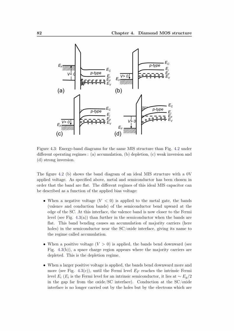
82 Chapter 4. Diamond MOS structure
EF EC
EV EF Ei
p-type V< 0
EF
EC
EV EF Ei
p-type
V> 0
EF
EC
EV EF Ei
p-type
V> 0
EF
EC
EV EF Ei
p-type
V> 0
(a)
(d) (c)
(b)
Figure 4.3: Energy-band diagrams for the same MIS structure than Fig. 4.2 under
different operating regimes : (a) accumulation, (b) depletion, (c) weak inversion and
(d) strong inversion.
The figure 4.2 (b) shows the band diagram of an ideal MIS structure with a 0V
applied voltage. As specified above, metal and semiconductor has been chosen in
order that the band are flat. The different regimes of this ideal MIS capacitor can
be described as a function of the applied bias voltage:
• When a negative voltage (V < 0) is applied to the metal gate, the bands
(valence and conduction bands) of the semiconductor bend upward at the
edge of the SC. At this interface, the valence band is now closer to the Fermi
level (see Fig. 4.3(a)) than further in the semiconductor when the bands are
flat. This band bending causes an accumulation of majority carriers (here
holes) in the semiconductor near the SC/oxide interface, giving its name to
the regime called accumulation.
• When a positive voltage (V > 0) is applied, the bands bend downward (see
Fig. 4.3(b)), a space charge region appears where the majority carriers are
depleted. This is the depletion regime.
• When a larger positive voltage is applied, the bands bend downward more and
more (see Fig. 4.3(c)), until the Fermi level EF reaches the intrinsic Fermi
level Ei (Ei is the Fermi level for an intrinsic semiconductor, it lies at Eg/2
in the gap far from the oxide/SC interface). Conduction at the SC/oxide
interface is no longer carried out by the holes but by the electrons which are

4.1. MOS concept and theory 83
more numerous than the holes in this region. The semiconductor is said locally
inverted and this regime is called the weak inversion.
• By increasing further the voltage, the strong inversion regime is reached (see
Fig. 4.3(d)). The sheet density of electrons in the inversion layer is now larger
than the density of holes in the neutral part of the semiconductor. Usually,
no distinction is made between weak and strong inversion regime and what
is often called inversion regime corresponds to strong inversion case defined
here.
4.1.2 QΨ graph : charges vs surface potential
Insulator p-semiconductor EC
EV
EF
Ei qΨB
qΨs
qΨp(x)
x
Eg
Figure 4.4: Energy band diagram at
the interface of a p-type semiconduc-
tor/insulator. The potential qΨp(x) is
measured with respect to the intrinsic
Fermi level Ei in the bulk at a distance
x from the insulator/SC interface. The
surface potential Ψs=Ψp(0) is the po-
tential at the interface. It corresponds
to the band curvature.
Several parameters are involved in the MOS structure operating such as dop-
ing and thickness of the semiconductor, thickness, permittivity, and charge of the
oxide, as well as the temperature. Gilbert Vincent proposed a single and simple
graph (named QΨ) of semiconductor charge versus the surface potential. This ap-
proach is very useful to understand MOS operation as well as the influence of each
fore-mentioned parameter on the MOS polarisation and thus to analyze C(V ) mea-
surements in terms of operating regimes. In this part, the fundamentals of the QΨ
approach will be described. If needed, more details can be found in the literature
[Vincent 2005, Vincent 2008].
4.1.2.1 Pre-requisites and hypothesis
Let’s consider a MOS structure composed of a metal, an oxide (thickness dox, per-
mittivity "ox) and a p-type semiconductor (permittivity "SC , doping Na). The gate
voltage VG is applied on the metal and the reference potential is taken at the back
side of the SC (as shown on the inset of fig. 4.6). The surface potential of the SC (at
the interface with the oxide) is noted Ψs and corresponds to the difference between
Ei in the bulk and at the interface as shown in figure 4.4. QASC is defined as the
surfacic total charge of the SC. For sake of simplicity, some assumptions have to be
made:
• the semiconductor doping level is constant,

84 Chapter 4. Diamond MOS structure
• the oxide is considered to be perfect : no charge inside within, and no current
flow through it,
• the flat band voltage, due to work function difference between oxide and SC
(and also to the charges in oxide and at the interface oxide/SC) is taken equal
to 0 V.
The goal of the following calculations is to obtain the charges repartition as function
of the applied gate voltage VG. Then, it will be obvious to obtain the corresponding
C(V) characteristics as C = dQ/dVG.
When a potential difference VG is applied between the metal and the SC, a charge
transfer occurs. If VG >0, electrons are transferred from the metal to the SC. They
are then in the SC near the SC/oxide interface while holes (same |Q|) are located
in the metal near metal/oxide interface to balance the electrons. An electric field is
induced by these charges.
Firstly, the expression of the SC total charge as a function of the SC surface potential
QSC(Ψs) has to be established in order to obtain the expression of QSC(VG).
4.1.2.2 QSC(Ψs)
Ψs has been defined as the surface potential of the SC. Ψb is defined as the potential
difference between the intrinsic level and the Fermi level (see Fig. 4.4) in the neutral
part of the SC (far from the oxide/SC interface), for a non degenerate SC such as:
Ψb =kT
qln
Na
ni
(4.1)
where ni is the SC intrinsic concentration, T the temperature, k the Boltzmann
constant and q=1.602 10−19 C the elementary charge. In the following, Ψp(x)
corresponds to the potential Ei(x)/q at the x abscissa (x=0 at oxide/SC interface)
with respect to the neutral region of the SC:
Ψp(x) =[Ei(x)− Ei(1)]
q(4.2)
At the SC surface Ψp(0) = Ψs, and far away from the surface, as it is defined with
respect to the intrinsic Fermi level Ψp(1)=0. The electron concentration np and
the hole concentration pp at x abscissa can be expressed as a function of Ψp and the
equilibrium densities of electron and holes in the neutral part of the SC. Thus the
total space charge density is given by:
(x) = q(N+D −N−
A + pp − np) (4.3)
The potential Ψp as a function of the abscissa x can be derived using the Poisson
equation :d2Ψp
dx2= −(x)
"SC(4.4)
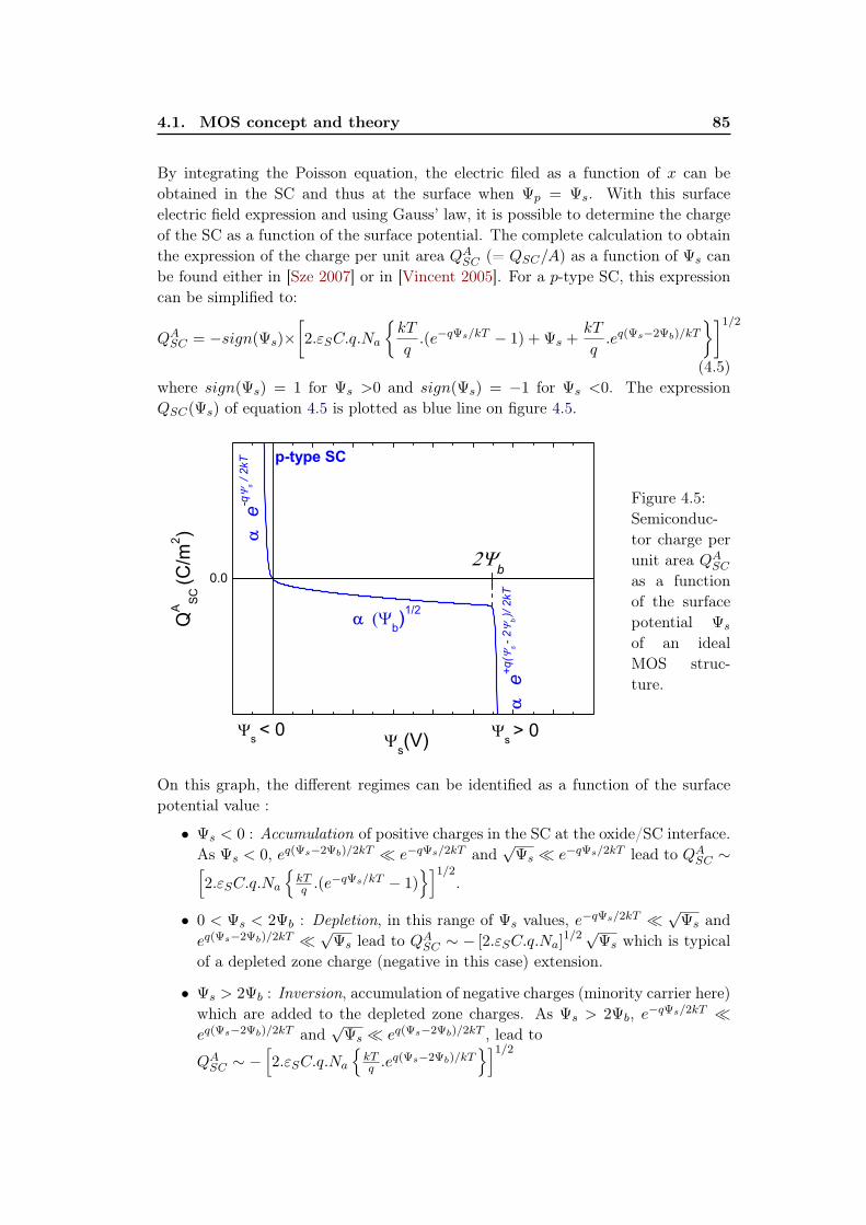
4.1. MOS concept and theory 85
By integrating the Poisson equation, the electric filed as a function of x can be
obtained in the SC and thus at the surface when Ψp = Ψs. With this surface
electric field expression and using Gauss’ law, it is possible to determine the charge
of the SC as a function of the surface potential. The complete calculation to obtain
the expression of the charge per unit area QASC (= QSC/A) as a function of Ψs can
be found either in [Sze 2007] or in [Vincent 2005]. For a p-type SC, this expression
can be simplified to:
QASC = −sign(Ψs)
2."SC.q.Na
kT
q.(e−qΨs/kT − 1) + Ψs +
kT
q.eq(Ψs−2Ψb)/kT
]1/2
(4.5)
where sign(Ψs) = 1 for Ψs >0 and sign(Ψs) = −1 for Ψs <0. The expression
QSC(Ψs) of equation 4.5 is plotted as blue line on figure 4.5.
Figure 4.5:
Semiconduc-
tor charge per
unit area QASC
as a function
of the surface
potential Ψs
of an ideal
MOS struc-
ture.
On this graph, the different regimes can be identified as a function of the surface
potential value :
• Ψs < 0 : Accumulation of positive charges in the SC at the oxide/SC interface.
As Ψs < 0, eq(Ψs−2Ψb)/2kT e−qΨs/2kT andpΨs e−qΨs/2kT lead to QA
SC h
2."SC.q.Na
n
kTq .(e−qΨs/kT − 1)
oi1/2.
• 0 < Ψs < 2Ψb : Depletion, in this range of Ψs values, e−qΨs/2kT pΨs and
eq(Ψs−2Ψb)/2kT pΨs lead to QA
SC − [2."SC.q.Na]1/2pΨs which is typical
of a depleted zone charge (negative in this case) extension.
• Ψs > 2Ψb : Inversion, accumulation of negative charges (minority carrier here)
which are added to the depleted zone charges. As Ψs > 2Ψb, e−qΨs/2kT
eq(Ψs−2Ψb)/2kT andpΨs eq(Ψs−2Ψb)/2kT , lead to
QASC −
h
2."SC.q.Na
n
kTq .eq(Ψs−2Ψb)/kT
oi1/2

86 Chapter 4. Diamond MOS structure
4.1.2.3 QSC(VG)
Metal Oxide
SC
VG
Figure 4.6: Graphical solution of SC charge per unit area as a function of gate
voltage VG for an ideal MOS structure (represented on the inset). QASC(Ψs) and
QASC(VG) are plotted respectively in blue and red.
In practical case, the operator cannot modify directly Ψs. The tunable parame-
ter is the gate voltage VG. That is why it is necessary to express the SC charge as
function of the gate voltage.
As the MOS structure is neutral, one can write QAM + QA
SC = 0, where QAM is
the metal surfacic charge. The electric field is equal to zero in the metal, and equal
to QAM/"ox at the metal/oxide interface. As there is no charge in the oxide, the
electric field is constant and equal to :
Eox =QA
M
"ox= −QA
SC
"ox(4.6)
As VG is the potential of the metal gate and Ψs the surface potential of the SC at
oxide/SC interface, the potential difference between the metal and the SC surface
can be written as a function of the electric field in the oxide and its thickness:
VG −Ψs = Eox.dox (4.7)
Combining Eq. 4.7 and Eq. 4.6, VG−Ψs can be expressed as function of SC charge:
VG −Ψs = −QASC
"ox.dox (4.8)
and thus, the expression of the SC charge as function of VG and Ψs is :
QASC =
"oxdox
(Ψs − VG) (4.9)
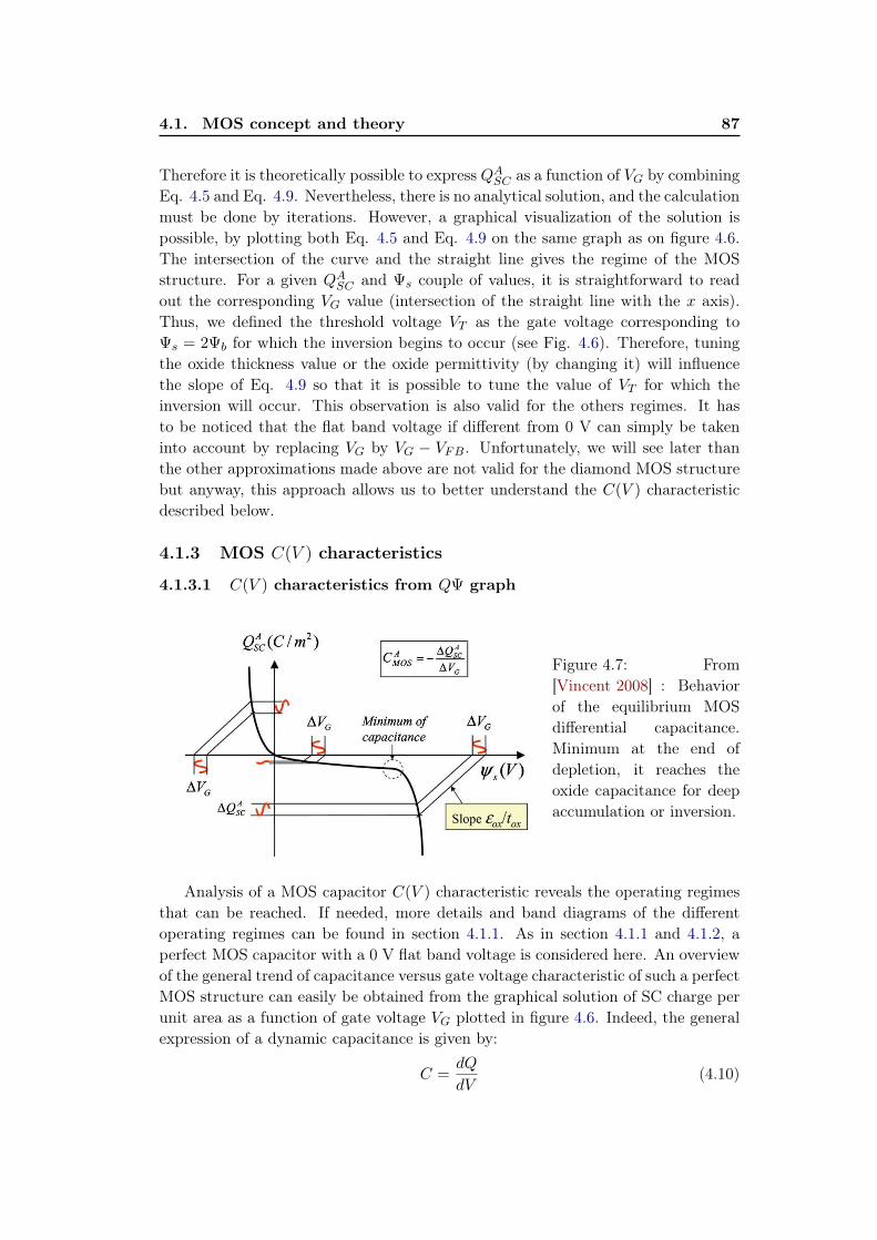
4.1. MOS concept and theory 87
Therefore it is theoretically possible to express QASC as a function of VG by combining
Eq. 4.5 and Eq. 4.9. Nevertheless, there is no analytical solution, and the calculation
must be done by iterations. However, a graphical visualization of the solution is
possible, by plotting both Eq. 4.5 and Eq. 4.9 on the same graph as on figure 4.6.
The intersection of the curve and the straight line gives the regime of the MOS
structure. For a given QASC and Ψs couple of values, it is straightforward to read
out the corresponding VG value (intersection of the straight line with the x axis).
Thus, we defined the threshold voltage VT as the gate voltage corresponding to
Ψs = 2Ψb for which the inversion begins to occur (see Fig. 4.6). Therefore, tuning
the oxide thickness value or the oxide permittivity (by changing it) will influence
the slope of Eq. 4.9 so that it is possible to tune the value of VT for which the
inversion will occur. This observation is also valid for the others regimes. It has
to be noticed that the flat band voltage if different from 0 V can simply be taken
into account by replacing VG by VG − VFB. Unfortunately, we will see later than
the other approximations made above are not valid for the diamond MOS structure
but anyway, this approach allows us to better understand the C(V ) characteristic
described below.
4.1.3 MOS C(V ) characteristics
4.1.3.1 C(V ) characteristics from QΨ graph
Figure 4.7: From
[Vincent 2008] : Behavior
of the equilibrium MOS
differential capacitance.
Minimum at the end of
depletion, it reaches the
oxide capacitance for deep
accumulation or inversion.
Analysis of a MOS capacitor C(V ) characteristic reveals the operating regimes
that can be reached. If needed, more details and band diagrams of the different
operating regimes can be found in section 4.1.1. As in section 4.1.1 and 4.1.2, a
perfect MOS capacitor with a 0 V flat band voltage is considered here. An overview
of the general trend of capacitance versus gate voltage characteristic of such a perfect
MOS structure can easily be obtained from the graphical solution of SC charge per
unit area as a function of gate voltage VG plotted in figure 4.6. Indeed, the general
expression of a dynamic capacitance is given by:
C =dQ
dV(4.10)
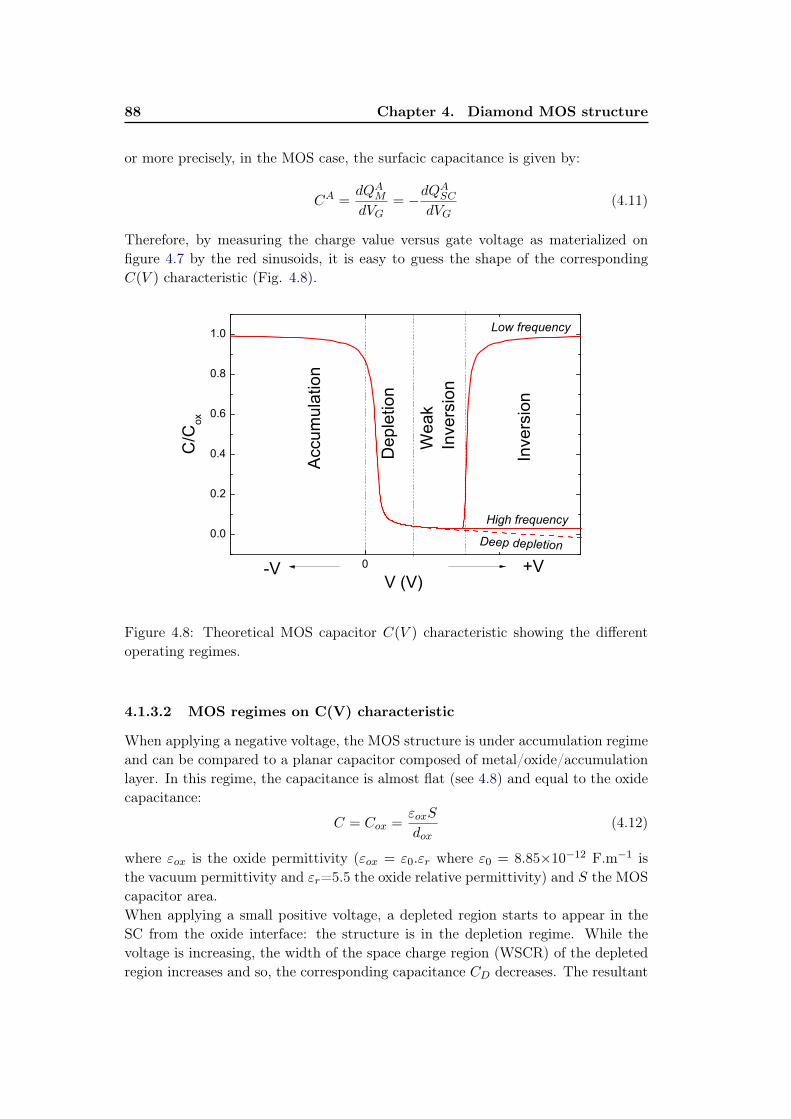
88 Chapter 4. Diamond MOS structure
or more precisely, in the MOS case, the surfacic capacitance is given by:
CA =dQA
M
dVG= −dQA
SC
dVG(4.11)
Therefore, by measuring the charge value versus gate voltage as materialized on
figure 4.7 by the red sinusoids, it is easy to guess the shape of the corresponding
C(V ) characteristic (Fig. 4.8).
0
0.0
0.2
0.4
0.6
0.8
1.0
Deep depletion
Low frequency
High frequency
C/C
ox
V (V)
We
ak
Inve
rsio
n
De
ple
tio
n
Accu
mu
latio
n
+V-V
Inve
rsio
n
Figure 4.8: Theoretical MOS capacitor C(V ) characteristic showing the different
operating regimes.
4.1.3.2 MOS regimes on C(V) characteristic
When applying a negative voltage, the MOS structure is under accumulation regime
and can be compared to a planar capacitor composed of metal/oxide/accumulation
layer. In this regime, the capacitance is almost flat (see 4.8) and equal to the oxide
capacitance:
C = Cox ="oxS
dox(4.12)
where "ox is the oxide permittivity ("ox = "0."r where "0 = 8.8510−12 F.m−1 is
the vacuum permittivity and "r=5.5 the oxide relative permittivity) and S the MOS
capacitor area.
When applying a small positive voltage, a depleted region starts to appear in the
SC from the oxide interface: the structure is in the depletion regime. While the
voltage is increasing, the width of the space charge region (WSCR) of the depleted
region increases and so, the corresponding capacitance CD decreases. The resultant

4.1. MOS concept and theory 89
capacitance of the whole structure is composed of the oxide capacitance Cox in series
with the depleted region capacitance CD such as :
1
C(V )=
1
Cox+
1
CD(V )(4.13)
Consequently, as Cox is a constant value, the total capacitance C(V ) decreases as
the voltage bias increases. If a larger positive voltage is applied, the structure should
be theoretically in weak inversion and then in strong inversion. Three cases can be
distinguished (as represented on 4.8):
• Low frequency case of inversion
In strong inversion regime (called usually inversion), the measured capacitance
versus bias voltage increases until reaching the oxide capacitance value due to
the presence of minority carriers at the interface. In fact, the structure is again
comparable to a planar capacitance composed of the metal/oxide/inversion
layer. For a MOS capacitor, this regime needs a minority carriers (here, elec-
trons) generation mechanism to be present. This can be provided by ther-
mal (or optical) generation of electron-hole pairs in the neutral part of the
semiconductor by intrinsic level or by mid gap deep level. Besides, thermal
generation depends on the band gap value (which is large for diamond). The
measurement frequency must therefore be very low, typically lower than 1 Hz
for silicon (which is a small band gap SC compared to diamond), in order that
the charges could follow the a.c signal. This is the low frequency case.
• High frequency case of inversion
If the frequency is too high, the recombination- generation rates of minority
carriers can not follow the a.c signal variation and lead to charge exchange
with the inversion layer. This last stays unchanged and no increase of the
capacitance is observed. Instead the capacitance measured stays constant :
this is the high frequency case of inversion.
• Deep depletion
If a high measurement frequency is combined with a quick VG sweeping rate (it
is commonly admitted that 1 hour, to sweep from accumulation to inversion,
can be quick for a good semiconductor), the inversion layer can not be formed
and instead, the depletion layer continues to extend in the semiconductor
(even if Ψs is larger than 2Ψb). In this case, the capacitance will continue to
decrease (/pVG). This regime is a non equilibrium state.
Thus, particular attention has to be paid to the measurement frequency depending
on the semiconductor used. In the case of diamond, due to its wide band gap, very
low frequency (n 1 Hz) will be necessary to observe low frequency inversion, if no
other minority carrier generation source is used. Therefore, only deep depletion is
expected in diamond.

90 Chapter 4. Diamond MOS structure
4.1.3.3 How charges and interfaces states affect experimental C(V ) char-
acteristics
In real cases, the experimental C(V ) characteristics differ from the perfect one
(described in section 4.1.3.1). Thus, when characterizing a real MOS structure,
several reasons can explain the difference between experimental C(V ) characteristics
and the theoretical ideal one:
• work function difference between metal and SC,
• fixed charges in the oxide,
• mobile charges in the oxide,
• interface states at oxide/SC.
The two first items result in a voltage shift of the C(V ) characteristics, while the
third one is responsible for an hysteresis behaviour. The fourth one, the interface
states, can affect the C(V ) characteristics in several ways. Three of them can be
detected to allow quantification of interface states in MOS structure [Schroder 2006,
Gourrier 1983]:
• on measured capacitance value :
if a state can follow the measurement signal frequency (generation/recombination
rate faster than the measurements frequency), it will contribute to the mea-
sured capacitance when the Fermi level at the interface will coincide with the
interface state density of states in the gap. Determination of interface state
density Nis from C value is only relevant for Nis larger than 1011 cm−2.eV−1.
• on measured conductance :
the conductance is equal to zero for an ideal MOS structure (perfect oxide =
infinite oxide resistance). If interface states exist, they will have an influence
on the conductance value, when the measurement frequency is comparable to
the inverse of the time constant related to the capture or emission of carrier by
or from this interface states. The influence of interface states is in theory easier
to measure on conductance G(!) than in capacitance C(!). As already men-
tioned, for an ideal MOS capacitance without interface state G(!)=0 (because
of the oxide insulation). Therefore, if interface states are present, they affect
directly the conductance value. While the measured capacitance C has con-
tribution from the oxide and the depleted region of the SC in addition to the
one of the interface states. Thus, the contribution of this last is more difficult
to distinguish from capacitance than from conductance. Methods based on
conductance, are complex to implement (measurements at different frequency
on several order of magnitude are needed) but can quantify lower interface
states densities than the previous one. In case of diamond, at the moment,
one cannot achieve sufficiently high quality oxide to use such a method.
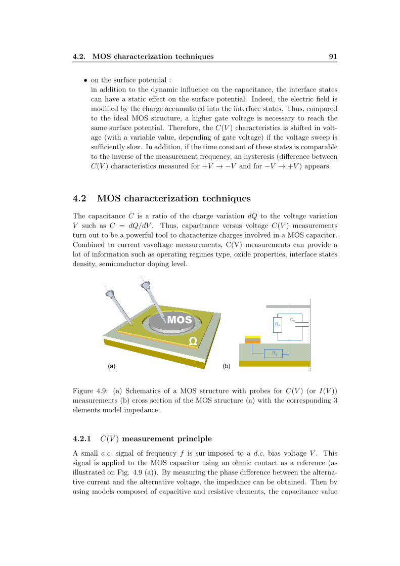
4.2. MOS characterization techniques 91
• on the surface potential :
in addition to the dynamic influence on the capacitance, the interface states
can have a static effect on the surface potential. Indeed, the electric field is
modified by the charge accumulated into the interface states. Thus, compared
to the ideal MOS structure, a higher gate voltage is necessary to reach the
same surface potential. Therefore, the C(V ) characteristics is shifted in volt-
age (with a variable value, depending of gate voltage) if the voltage sweep is
sufficiently slow. In addition, if the time constant of these states is comparable
to the inverse of the measurement frequency, an hysteresis (difference between
C(V ) characteristics measured for +V ! −V and for −V ! +V ) appears.
4.2 MOS characterization techniques
The capacitance C is a ratio of the charge variation dQ to the voltage variation
V such as C = dQ/dV . Thus, capacitance versus voltage C(V ) measurements
turn out to be a powerful tool to characterize charges involved in a MOS capacitor.
Combined to current vsvoltage measurements, C(V) measurements can provide a
lot of information such as operating regimes type, oxide properties, interface states
density, semiconductor doping level.
MOS
!
RS
RP CP
(a) (b)
Figure 4.9: (a) Schematics of a MOS structure with probes for C(V ) (or I(V ))
measurements (b) cross section of the MOS structure (a) with the corresponding 3
elements model impedance.
4.2.1 C(V ) measurement principle
A small a.c. signal of frequency f is sur-imposed to a d.c. bias voltage V . This
signal is applied to the MOS capacitor using an ohmic contact as a reference (as
illustrated on Fig. 4.9 (a)). By measuring the phase difference between the alterna-
tive current and the alternative voltage, the impedance can be obtained. Then by
using models composed of capacitive and resistive elements, the capacitance value

92 Chapter 4. Diamond MOS structure
can be extracted. By varying the d.c bias voltage V , C(V ) characteristics can be
plotted.
4.2.2 Impedance model
The selection of the impedance model to extract the capacitance from the impedance
measurement is not trivial and has to be done by carefully analyzing the structure
to characterize. Diamond material, particularly at low doping level, has a high
resistivity due to the high ionization energy of the boron dopant ( >100 S/cm
for a diamond with [B]=21017 cm−3 and a compensation ND=[B]/10, see 1.6).
This resistance of diamond, referred as series resistance Rs in the following, has to
be taken into account as it will limit the current flowing in the stack composed of
gate/oxide/diamond/ohmic contact as shown on figure 4.9. In addition, in most of
the practical cases, the oxide won’t be a perfect insulator with an infinite resistance.
This resistance has a finite value which has to be considered through what will be
called the parallel resistance Rp as illustrated on figure 4.9 (b).
4.2.2.1 Series or parallel model ?
A complex number impedance Z(!) is obtained from measurement of the phase
difference between an a.c. current I(!) and an a.c. voltage such as :
V (!) = Z(!).I(!) (4.14)
where ! the pulsation corresponding to the measurement frequency (! = 2f) and
Z(!) = R(!) + jX(!) (4.15)
with j the imaginary unit, R(!) the real part and X(!) the imaginary part. Models
composed of capacitive and resistive elements are needed to extract capacitance
value from this complex impedance. The two main approximations are called:
• series model : a resistance Rs in series with a capacitance Cs as represented
on Fig. 4.10 (a), for which the impedance can be expressed :
Z(!) = Rs +1
jCs!= Rs −
j
Cs!(4.16)
• parallel model : a resistance Rp in parallel with a capacitance Cp as represented
on Fig. 4.10(b). The corresponding equivalent impedance is :
1
Z(!)=
1
Rs+ jCp! , Z(!) =
Rp
1 + (RpCp!)2− j
CpR2p!
1 + (RpCp!)2(4.17)
Unfortunately, these models are too approximative and have to be used with a
great carefulness with diamond. Indeed, neither a series model nor a parallel model
is sufficiently accurate to model diamond MOS structure such as represented on

4.2. MOS characterization techniques 93
RP CP
RS
CS
RS
CP RP
(a) (b) (c)
Figure 4.10: (a) Series, (b)
parallel, and (c) 3 elements
models that can be used
to extract capacitance from
impedance measurement.
Fig. 4.9 (b). Due to the high ionization of diamond (which induced a non negligible
series resistance) and to the leakage of the oxide (modeled by a resistance in parallel
to the capacitance), at least a three element model must be considered. For the 3
elements model represented on figure 4.10 (c), the equivalent impedance is:
Z(!) = Rs +Rp
1 + (RpCp!)2− j
CpR2p!
1 + (RpCp!)2(4.18)
This three elements model is more appropriate for MOS diamond structure as illus-
trated on figure 4.9 (b).
4.2.2.2 Two frequency measurement
As shown previously, in most of the cases, samples can not be modeled by a simple
series or parallel models. A three elements models is better suited. A two frequency
measurement method allows to extract the capacitance value C of a three elements
models by using the simple series models at two frequencies. Let’s consider notations
R C
rS
CS1
RS1
(b) (a)
CS2
RS2
(c)
f1 f2
Figure 4.11: Notations and
impedance models used in two
frequency measurements meth-
ods: (a) three elements model
corresponding to the MOS
structure, (b) & (c) the se-
ries models measured at two
frequencies to extract value of
model (a).
given in figure 4.11: value subscripted 1 corresponds to measurement performed at
a frequency f1 (idem for f2). Two frequency measurements performed with a simple
series model allow theoretically to extract the value of each element from a three
elements circuit. The equivalent impedance of the three elements circuit represented

94 Chapter 4. Diamond MOS structure
on Fig. 4.11 (a) is:
Z(!) = rS +R
1 + (RC!)2− j
R2C!
1 + (RC!)2(4.19)
The equivalent impedance of a series model is:
Z(!) = Rs +1
jCs!(4.20)
If we equalize the imaginary parts of Eq. 4.19 and Eq. 4.20, we obtain:
1 + (RC!)2
R2C!= Cs! (4.21)
By performing measurements at 2 frequencies (!1 = 2f1 and !2 = 2f2) and by
making the difference between the obtained results, one finds:
Cs1!21 − Cs2!
22 =
R2C2(!21 − !2
2)
R2C(4.22)
Then, it is possible to derive C as a function of Cs1, Cs2, f1 and f2 only:
C =Cs1f
21 − Cs2f
22
f21 − f2
2
(4.23)
Thus, by performing measurements at two frequencies it is possible to use simple
series model to extract capacitance value of a three elements circuita.
4.2.2.3 Nyquist and Cole-Cole plot
Impedance measurements versus frequency combined to the appropriate model are
very useful to determine the influence of each element: oxide leakage (modeled by
Rp) and diamond series resistance (Rs). Nyquist (plot of the impedance real part
R and the opposite of the impedance imaginary part −X as a function of the fre-
quency) and Cole-Cole diagrams (plot of −X versus R from a Nyquist measurement)
performed on a typical diamond MOS structure (such as the one represented on fig-
ure 4.9) are plotted on figure 4.12 (a) and (b). These measurements were undertaken
under a bias voltage leading to an accumulation regime, so that the experimental
data could be fitted using the 3 elements impedance model (equation 4.19). As can
be seen, the theoretical model is well adapted in this regime. When increasing the
bias voltage under which the measurements are performed, the model is no longer
valid (not shown here) because of the depleted region which adds a capacitance CD
in series of the previous three elements model.
The Nyquist plot allows to determine easily the frequency for which the imaginary
part of the impedance could be more accurately measured and so the capacitance
aSimilar calculations can be also done with a parallel model.

4.2. MOS characterization techniques 95
102
103
104
105
106
100
101
102
103
104
105
0 1x10⁴
2x10⁴
3x10⁴
0
1x10⁴
2x10⁴
3x10⁴
(b)
R
-X
fit R
fit X
R
(Ω)
; -X
(Ω)
frequency (Hz)
V= -5V
(a)
fit
exp
-X(Ω
)
R(Ω)
V=-5V
f Rs+Rp Rs
Figure 4.12: (a) Real part R and imaginary part −X of the impedance versus
frequency experimental and fitted data at -5 V bias voltage and (b) Cole-Cole plot
of (a) data and the corresponding fit for a diamond MOS structure (sample #2).
value extracted with more precision: when the ratio −X/R is the highest. The
Cole-Cole plot gives quickly, even without fitting the data, an idea of series resis-
tance Rs (corresponding to the diamond series resistance) and parallel resistance
(evaluating of the oxide leakage):
• At high frequency such as f / 1/2RpCp (left part of the half circle) the
equivalent impedance tends to Rs as the denominator 1 + (RpCp!)2 tends
toward infinity in equation 4.19. In terms of equivalent circuit (see Fig. 4.10
(c)), at high frequency the capacitance Cp short circuits Rp so that, the
equivalent impedance is Rs. By reading the crossing of the half circle plot
with the x axis (R value) at high frequency, the series resistance Rs can be
determined directly.
• At very low frequency such as f 1/2RpCp (right part of the half circle),
the imaginary part term in equation 4.19 becomes negligible compared to Rp
and the real part tend toward Rs + Rp. In terms of equivalent circuit (see
Fig. 4.10 (c)), Cp acts as an open circuit and the equivalent impedance tends
to Rs+Rp. Consequently, Rs+Rp value can be determined directly from the
intersection of the Cole-Cole plot with the x axis.
Additionally, by fitting the experimental data with equation 4.19 (full lines on fig-
ures 4.12), the capacitance value Cp can be obtained. For the data shown here,
parallel resistance is equal to 28 kΩ (this corresponds to a quite leaky oxide) while
series resistance is equal to 4 kΩ and Cp=1.510−11F.
Additional capacitances due to interface states or charges in the oxide also make
the equivalent model more complex. Therefore, as far as possible, we will try to get

96 Chapter 4. Diamond MOS structure
closer to the simplest case when performing C(V) measurements. For instance, if
the serial resistance of diamond is negligible in regards to the parallel resistance of
the oxide (i.e. Rs Rp), the simple parallel model give directly good evaluation of
the MOS structure capacitance.
4.2.3 Experimental setup
The electrical properties of the MOS capacitances have been measured using a Keith-
ley 6517B source-electrometer apparatus for the static current/voltage I(V) char-
acteristics and a Agilent E4980A Precision LCR Meter for the capacitance/voltage
C(V) measurements. Frequency dependent capacitance measurements have been
performed with a.c. signal frequency ranging from 100 Hz to 2 MHz and typical
amplitude of 50 mV. A Solartron Modulab-MTS system was also used for advanced
C(V ) at very low frequency (down to 1 Hz).
Figure 4.13: Picture of the experimental set-up used for C(V) and I(V) measure-
ments. The sample is put into the metallic box (vacuum and T-controled). Using
the binocular, probe tips (inset) can be placed accurately on the sample.
4.3 MOS fabrication using diamond semiconductor
The main problem to fabricate a MOS structure is to achieve the semiconductor
oxide interface with a sufficiently low interface states density. In that case, the
different regimes of the MOS can be controlled: accumulation of majority carriers,
depletion, deep depletion or inversion of carriers. In most cases and contrary to
the Si/Oxide interface, the too large density of interface states within the gap are
charging under bias voltage, and the breakdown field of the oxide is reached before

4.3. MOS fabrication using diamond semiconductor 97
deep depletion or inversion regimes. Also, previous MOS structures performed on
diamond [Hirama 2006, Hirama 2010, Kasu 2012, Kawakami 2005] exhibited an ac-
cumulation regime but no deep depletion or inversion regimes. MOS structures on
diamond using high dielectric constant Ta2O5 oxides were also reported [Cheng 2012]
but did not show the deep depletion regime. In our case, in order to reach deep
depletion or inversion regimes at the oxide diamond interface, we proposed an ap-
proach combining Aluminum oxide (Al2O3) deposited by atomic layer deposition
(ALD) at low temperature on an oxygen-terminated diamond (patent [Chicot 2011],
[Chicot 2013]). Thanks to the electronic affinity value (qχ= 1.7 eV [Maier 2001]) of
oxygen-terminated diamond and to the band gap values of Al2O3 deposited by low
temperature ALD [Huang 2009, Nohira 2002], a good match between Al2O3 band
gap and oxygen-terminated diamond could theoretically be obtained (cf. figure 4.1).
Such an approach is innovative, as ALD technique is commonly used on hydrogen-
terminated diamond surface instead of oxygen terminated one. For example, recent
works reported investigation of Al2O3 deposited by Atomic Layer Deposition (ALD)
on hydrogen-terminated diamond to stabilize [Hiraiwa 2012] or to study the band
offsets [Liu 2012] related to the hydrogen 2-D gas.
In this section further details on oxygen surface treatment of diamond and ALD
of aluminum oxide will be given. Then, the MOS capacitor design used in this work
as well as the samples will be presented.
4.3.1 Low temperature ALD on oxygenated diamond surface
4.3.1.1 Oxygenation of surface
Right after growth, diamond surface is H-terminated due to the presence of hy-
drogen in the gas phase (carrier gas). As already mentioned in this work, hydrogen
terminations can be useful (H-terminated diamond FET) but can also be responsible
of parasitic conduction (when not wanted) as the main conduction channel. In fact,
when H-terminated, a 2D hole gas is formed at the diamond surface, which could
lead to interface and surface states not desired for a MOS structure. Therefore,
it has been chosen to oxygenate all our samples by an oxygenation treatment. In
addition to its electron affinity value which allows a good match between Al2O3 and
diamond band diagram (diamond gap "included" within the Al2O3 gap, see figure
4.1), oxygen-terminated diamond surface also offers a good stability and cleanliness
for the oxide/diamond surface. Hydrogen terminated diamond surface is not sta-
ble and becomes oxygen terminated naturally in air. However, this process is very
slow. Thus, technological processes have been developed to control this oxygena-
tion in order to obtain oxygenated diamond surface (for Hall bars, Schottky diodes
and MOS). This can be done by chemical treatments, by exposition to an oxygen
plasma or even by UV ozone treatment [Teraji 2008, Teraji 2009]. This last treat-
ment has been shown to be very efficient to achieve low leakage Schottky diodes
[Teraji 2009]. However, the principle and the experimental set-up are rather simple.

98 Chapter 4. Diamond MOS structure
The sample is put in a chamber under secondary vacuum. O2 gas is introduced in
the chamber (500 mBars) and exposed to a deep UV light during 90 minutes. All
the samples of this work were treated by deep UV Ozone except one by reactive ion
etching oxygen plasma (in the later case, the recipe was chosen to not etch diamond).
X-Ray photoelectron spectrometry studies performed on diamond samples treated
either by deep UV ozone [Boukherroub 2005] or O2 plasma [Hoeb 2010] showed that
the resultant surfaces are principally composed of hydroxyl terminations (-C-O-H)
but also of carbonyl ones (-C=O) as schematized on figure 4.14.
Diamond surface
O
H
C C
O
C
Figure 4.14: Schematic a diamond surface oxygenated by deep UV ozone treatment
or O2 plasma presenting hydroxyl terminations (-C-O-H) but also of carbonyl ones
(-C=O).
4.3.1.2 Atomic layer deposition
ALD is a deposition technique which has the specificity to deposit atomic layer by
atomic layer. Consequently, the deposited layer is formed and can fit closely any type
of shape. This process is based on sequences of precursors reaction which require,
for Al2O3 deposition, H-terminations at the surface in order that the reaction be
initialized. In our case, the diamond surface was oxygenated before oxide ALD.
This surface treatment led mostly to hydroxyl terminations (-C-O-H), which are
known to favor aluminum oxide deposition by ALD. The precursor used here was
trimethylaluminum (TMA), and the oxidant was H2O. A schematic of ALD of Al2O3
sequence is shown on figure 4.15. The reaction chamber is under a controlled 15
sccm flow of nitrogen. First, (a) a pulse of TMA is introduced in the chamber
and (b) reacts with hydroxyl terminations of diamond to form the first atomic layer
until saturation occurs (all terminations occupied). Then, the unused precursors are
pumped out from the chamber (not shown here). (c) A pulse of water is introduced
and (d) forms the second atomic layer. Water molecules that did not react are
pumped out. The surface is again composed of H-terminations. Thus, the (a), (b),
(c) and (d) steps are repeated as many times as atomic layers of Al2O3 are wanted.
As mentioned before an oxygen-terminated diamond surface is mostly composed
of hydroxyl terminations but also of few carbonyl. Such a defect is represented
on figure 4.15 (a). As the reaction is initialized thanks to hydroxyl terminations,
it was supposed that unwanted (-C=O) terminations would not allow the TMA
to decompose and form the Al-O bond. Typical pulse duration for precursors and

4.3. MOS fabrication using diamond semiconductor 99
oxidant are 0.015 s. Pumping steps duration can vary depending on the recipe but is
often set at 5 s. A longer pumping step (15 s, 30 s) allows to evacuate more efficiently
unused precursors in order to obtain better oxide quality. Indeed, unused precursors
or oxidant can led to mobile or fixed charge in the oxide. All the deposition of Al2O3
were performed at 100 C, insuring the growth of an amorphous layer. Such low
temperature is also compatible with the resist deposited before to delimitate the
pattern. The ALD system used in the present experiments was Savannah 100 from
Cambridge NanoTech.
Diamond surface
O
H
C Al
H
HH
Trimethyl
aluminium
O
C
Al
H
HH
H
O
Al
H HO
H2O
O
Al
H
O O
O
(a)
(b)
(c)
(d)
O
Al
O O
O
(e)
Diamond surface
Diamond surface
Diamond surface
C
C
C
Diamond surface
C C C C C C
C
Figure 4.15: Schematic Atomic Layer Deposition steps process of aluminum oxide on
oxygen-terminated diamond surface. The precursor is trimethylaluminium (TMA)
and the oxidant is water. (a) TMA pulse on hydroxyl terminated diamond surface
(b) formation and saturation of the first atomic layer (c) H2O pulse (d) formation
of the second atomic layer (e). The 4 previous steps are repeated as many times
as atomic layers of Al2O3 are wanted. A carbonyl group which is a typical defect
on oxygen terminated diamond is materialized on this schematic and is supposed to
not react with TMA.
4.3.2 MOS capacitor design
For sake of simplicity, a simple co-planar MOS capacitor design was chosen, i.e.
the MOS capacitor and the ohmic contact are on the same surface as illustrated
on figure 4.9 (a). Titanium/platinum/gold metal stack (e-beam evaporated), which
surrounds the MOS capacitor, is deposited through a window of resist. After lift
off, this metal stack is annealed in order to create an ohmic contact by forming
titanium carbide at the Ti/diamond interface. Another lithography step is used
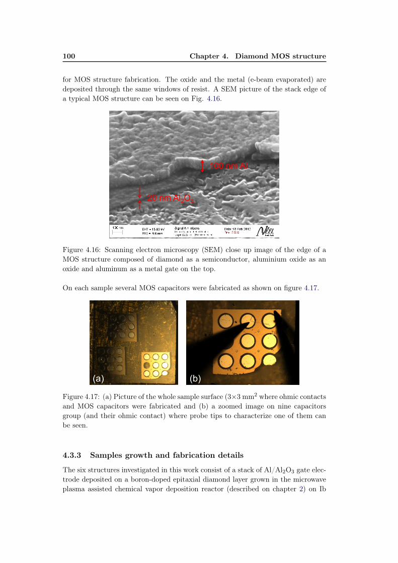
100 Chapter 4. Diamond MOS structure
for MOS structure fabrication. The oxide and the metal (e-beam evaporated) are
deposited through the same windows of resist. A SEM picture of the stack edge of
a typical MOS structure can be seen on Fig. 4.16.
100 nm Al
20 nm Al2O
3
Figure 4.16: Scanning electron microscopy (SEM) close up image of the edge of a
MOS structure composed of diamond as a semiconductor, aluminium oxide as an
oxide and aluminum as a metal gate on the top.
On each sample several MOS capacitors were fabricated as shown on figure 4.17.
(a) (b)
Figure 4.17: (a) Picture of the whole sample surface (33 mm2 where ohmic contacts
and MOS capacitors were fabricated and (b) a zoomed image on nine capacitors
group (and their ohmic contact) where probe tips to characterize one of them can
be seen.
4.3.3 Samples growth and fabrication details
The six structures investigated in this work consist of a stack of Al/Al2O3 gate elec-
trode deposited on a boron-doped epitaxial diamond layer grown in the microwave
plasma assisted chemical vapor deposition reactor (described on chapter 2) on Ib
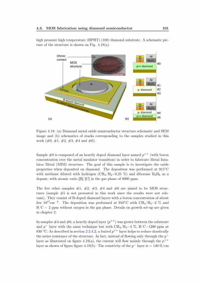
4.3. MOS fabrication using diamond semiconductor 101
high pressure high temperature (HPHT) (100) diamond substrate. A schematic pic-
ture of the structure is shown on Fig. 4.18(a).
100µm
Ohmic
contact MOS
structure
!"#$%&'()$#
!**#$%&'()$#
Al2O3
Al
!**#$%&'()$#
!"#$%&'()$#
+,###
+-##
+.#
+/#
0&1# 021#
+3#Ti Pt Au
Al2O3
Al
Ti Pt Au
Al2O3
Al
Ti Pt Au
+4#
Figure 4.18: (a) Diamond metal oxide semiconductor structure schematic and SEM
image and (b) schematics of stacks corresponding to the samples studied in this
work (#0, #1, #2, #3, #4 and #6).
Sample #0 is composed of an heavily doped diamond layer named p++ (with boron
concentration over the metal insulator transition) in order to fabricate Metal Insu-
lator Metal (MIM) structure. The goal of this sample is to investigate the oxide
properties when deposited on diamond. The deposition was performed at 915C
with methane diluted with hydrogen (CH4/H2=0.25 %) and diborane B2H6 as a
dopant, with atomic ratio [B]/[C] in the gas phase of 8000 ppm.
The five other samples #1, #2, #3, #4 and #6 are aimed to be MOS struc-
tures (sample #5 is not presented in this work since the results were not rele-
vant). They consist of B-doped diamond layers with a boron concentration of about
few 1017cm−3. The deposition was performed at 910C with CH4/H2=2 % and
B/C = 2 ppm without oxygen in the gas phase. Details on growth set-up are given
in chapter 2.
In samples #4 and #6, a heavily doped layer (p++) was grown between the substrate
and p− layer with the same technique but with CH4/H2=4 %, B/C=1200 ppm at
830 C. As described in section 2.2.4.2, a buried p++ layer helps to reduce drastically
the series resistance of the structure. In fact, instead of flowing only through the p−
layer as illustrated on figure 4.19(a), the current will flow mainly through the p++
layer as shown of figure figure 4.19(b). The resistivity of the p− layer is 140 Ω/cm

102 Chapter 4. Diamond MOS structure
Sample Doping dp−diamond Surface dAl2O3dAl
(cm−3) (nm) treatment (nm) (nm)
#0 >51020a 50a DUV O3 20a 100a
#1 31017b 1800b DUV O3 10a 100a
#2 31017b 1800b O2 plasma 20a 100a
#3 3.61017c 300a DUV O3 20a 100a
#4 2.21017c / >51020a 300a/150a DUV O3 20a 100a
#6 3.71017c / >51020a 300a/150a DUV O3 20a 15a
Table 4.1: Physical properties of metal/oxide/diamond structures.
aEstimated from growth conditions.bEstimated from SIMS measurements.cMeasured by C(V) measurements.
while the resistivity of the p++ layer is 0.4 Ω/cm (from figure 1.6). Therefore it
can be estimated that Rp− / 2rp− + Rp++. Thus the access resistance is reduced
thanks to the p++ layer and can be negligible in comparison to the resistance of a
good oxide. This will simplify the analysis by allowing to use a parallel model for
capacitance measurements but, from a material point of view, it could lower the top
surface quality of the p− layer. That is why sample #3 was grown without a buried
p++ layer but with the same p− layer thickness.
p++#
p$##
(b)
Al2O3
Al
Ti Pt Au
p$#
#1
#2
#3
Al2O3
Al
Ti Pt Au
(a)
#4
#6
Rp-
rp- rp- Rp++
20 µm
300 nm
Figure 4.19: Illustration of the conduction path in MOS structures (a) without and
(b) with a buried p++ layer.
On each sample, ohmic contacts (Ti/Pt/Au annealed at 750 C under high vac-
uum) were evaporated directly on the epitaxial layer to act as reference contact
for capacitance measurement. Photolithography process was used in order to selec-
tively deposit the dielectric oxide. Before that step, diamond surface oxygenation
was performed by two techniques: i) for sample #0, #1, #3, #4 and #6 by using

4.4. MOS operating regimes 103
deep UV ozone treatment [Teraji 2008], ii) for sample #2 by using oxygen RIE
plasma treatment. Then, the 10 nm for sample #1 and 20 nm for #0, #2, #3,
#4 and #6 of Al2O3 were deposited by ALD. In order to preserve the lithogra-
phy resist, the ALD oxide was deposited at low temperature (100C). Using the
same resist window (part of the sample surface without resist), the oxide was cov-
ered by a 100 nm thick aluminum metal using electron beam evaporator except for
sample #6. On the later, only 15 nm were deposited in order to obtain a UV semi-
transparent aluminum contact for light excitation. Schematics for each sample stack
can be found on figure 4.18. Parameters such as thickness (dp−diamond) and doping
of diamond layer, surface treatment and oxide thickness are summarised in table 4.1.
Al2O3 breakdown field value was reported to be 5 MV/cm [Groner 2004]. Thus,
due to the thickness of Al2O3 deposited (20 nm in most of the samples), the C(V )
measurements will be performed between -10 V and 10 V. Measurements performed
at higher voltage caused damages to the MOS capacitors.
4.4 MOS operating regimes
Sample #0 is a MIM structure while the five other samples are MOS structures.
On samples #1, #2 and #3, different oxide thicknesses and surface treatments were
tested (see table 4.1). In sample #3, the quality of the p− diamond surface has
been improved (with respect to #1 and #2), principally by reducing the thickness
of the layer. Samples #4 and #6 are the same than #3, but with an additional p++
buried layer in order to reduce the series resistance making the C(V ) measurements
and their interpretation simpler. The results will be presented in this order.
4.4.1 Oxide characterization using MIM structure : sample #0
-10 -5 0 5 100
20
40
60
80
100
10210
310
410
510
610
70
20
40
60
80
100
100 kHz
Ca
pa
cita
nce
(p
F)
Vbias
(V)
(b)
Ca
pa
cita
nce
(p
F)
frequency (Hz)
(a)
Figure 4.20: Capacitance (a) versus frequency (at Vbias = -5V) and (b) versus voltage
of a MIM structure (sample #0 made of Al/Al2O3/p++ diamond).
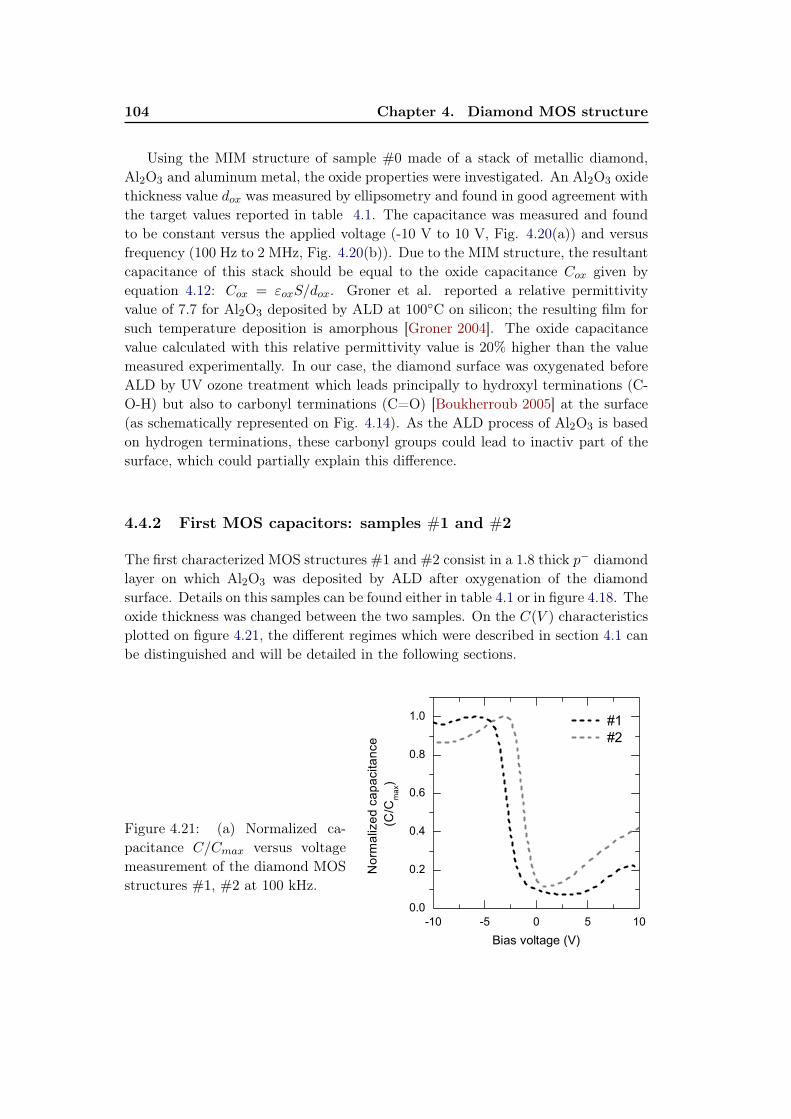
104 Chapter 4. Diamond MOS structure
Using the MIM structure of sample #0 made of a stack of metallic diamond,
Al2O3 and aluminum metal, the oxide properties were investigated. An Al2O3 oxide
thickness value dox was measured by ellipsometry and found in good agreement with
the target values reported in table 4.1. The capacitance was measured and found
to be constant versus the applied voltage (-10 V to 10 V, Fig. 4.20(a)) and versus
frequency (100 Hz to 2 MHz, Fig. 4.20(b)). Due to the MIM structure, the resultant
capacitance of this stack should be equal to the oxide capacitance Cox given by
equation 4.12: Cox = εoxS/dox. Groner et al. reported a relative permittivity
value of 7.7 for Al2O3 deposited by ALD at 100C on silicon; the resulting film for
such temperature deposition is amorphous [Groner 2004]. The oxide capacitance
value calculated with this relative permittivity value is 20% higher than the value
measured experimentally. In our case, the diamond surface was oxygenated before
ALD by UV ozone treatment which leads principally to hydroxyl terminations (C-
O-H) but also to carbonyl terminations (C=O) [Boukherroub 2005] at the surface
(as schematically represented on Fig. 4.14). As the ALD process of Al2O3 is based
on hydrogen terminations, these carbonyl groups could lead to inactiv part of the
surface, which could partially explain this difference.
4.4.2 First MOS capacitors: samples #1 and #2
The first characterized MOS structures #1 and #2 consist in a 1.8 thick p− diamond
layer on which Al2O3 was deposited by ALD after oxygenation of the diamond
surface. Details on this samples can be found either in table 4.1 or in figure 4.18. The
oxide thickness was changed between the two samples. On the C(V ) characteristics
plotted on figure 4.21, the different regimes which were described in section 4.1 can
be distinguished and will be detailed in the following sections.
Figure 4.21: (a) Normalized ca-
pacitance C/Cmax versus voltage
measurement of the diamond MOS
structures #1, #2 at 100 kHz.

4.4. MOS operating regimes 105
4.4.2.1 Accumulation regime and frequency dependent capacitance value
For negative voltage (V . −5 V for #1 and V . −3 V for #2), the accumulation of
holes is observed. This regime is characterized by an almost flat capacitance theo-
retically equal to that of the oxide capacitance Cox (Eq. 4.12) because the stack can
be viewed as a planar capacitance (see Fig. 4.28 (a)) composed of the oxide layer
between two electrodes (Al and diamond). But experimental capacitances in the ac-
cumulation regime take values above or below the expected Cox value depending on
the measurement frequency as plotted for sample #2 on figure 4.22. Nyquist plots
and Cole-Cole diagrams performed on sample #2 (plotted on Fig. 4.12) show a
good agreement with a three element circuit in the accumulation regime. Therefore,
such a circuit has been used to reproduce the series resistance effect on the mea-
surement. Indeed, in the ideal case, the capacitance is considered in parallel to the
resistance of the oxide (leakage current through the oxide) leading to a two elements
circuit. In our structure, the series resistance of the p-type diamond layer Rs = 4 kΩ
(estimated from Cole-Cole diagram) cannot be neglected (and must be considered
in series with the two elements impedance) with respect to the parallel resistance,
evaluated at 28 kΩ. Nevertheless, even applying a two frequency correction method
[Yang 1999] to the measurements plotted on figure 4.22 for a three elements circuit
(described in subsection 4.2.2.2), this frequency dispersion still exists, showing that
this unexpected behavior cannot be attributed exclusively to a non negligible series
resistance.
-10 0 10
101
102
103
104
105
800 kHz
500 kHz
400 kHz
200 kHz
100 kHz
50 kHz
25 kHz
10 kHz
C(p
F)
V (V)
f
5 kHz
Figure 4.22: C(V ) charac-
teristics of MOS structure
#2 measured at differ-
ent frequencies ranging
between 5 kHz and 800
kHz using a series model
impedance.
The capacitance can also be extracted from fits with the three elements model of the
Nyquist plot as described in section 4.2.2.3. This was performed for sample #2 at
V = -5 V as shown on figure 4.12. The resulting capacitance value was 1.510−11 F,

106 Chapter 4. Diamond MOS structure
which is almost ten times lower than the expected value for the oxide capacitance.
An additional impedance, due to interface states or/and deep levels in the diamond
layer close to the Al2O3/diamond interface (compensating levels in the first hundred
nanometers under Al2O3/diamond interface in a diamond growth without oxygen
in the gas phase [Muret 2008, Muret 2011, Muret 2010]), could be responsible for
this phenomenon.
However, if the accumulation capacitance values of samples #1 and #2 are com-
pared at a similar measurement frequency, the capacitance value of sample #1 is
higher than that of sample #2. This is in agreement with the oxide thickness values
of 10 nm and 20 nm used for samples #1 and #2 respectively. Nevertheless, the
capacitance value of #1 is more than twice higher than the capacitance value of
#1, confirming that another impedance than that of the oxide contribute to the
capacitance measured in accumulation.
4.4.2.2 Depletion regime
While the bias voltage increases, a space charge region begins to appear in the
semiconductor (Fig. 4.28(c)), the resulting capacitance corresponding to that mea-
sured in accumulation, in series with that of the space charge region, resulting in a
decrease of the total capacitance.
4.4.2.3 Inversion regime ?
For positive voltage values (V & 3 V for #1 and V & 2 V for #2), the capacitance
increases again (see Fig. 4.21). Usually, an increase in capacitance in this voltage
range is characteristic of the strong inversion regime where the type of the majority
carriers is locally (near oxide/semiconductor interface) inverted, meaning that the
electron concentration at the oxide/diamond interface is larger than the hole con-
centration in p-type diamond region. This regime needs a minority carriers (here
electrons) generation mechanism to be observed. Minority carriers can be provided
by thermal or optical generation of electron-hole pairs in the neutral part of the
semiconductor but frequency of the a.c signal used to measure the capacitance (f
= 100 kHz) must be sufficiently low to be comparable to the inverse time constant
related to the generation mechanism in order that the charges could follow this a.c
signal. In our case, no optical excitation was used and the frequency is too high for
thermal generation. Diamond p− layer of these two samples show a large amount
of extended structural defects such as hillocks (see Fig. 4.23) which are generally
going through the whole depth of the layer. The probability for hillocks appearance
is higher for thicker layers. A mechanism providing electrons from neutral regions
through these defects up to the oxide/semiconductor interface could be responsible
of this electron generation. However, a measurement artifact due to the high oxide
leakage current (figure 4.27 (c)) or an impedance due to deep levels (as suggested
above) can not be discarded.

4.4. MOS operating regimes 107
(a) (b) (c)
Figure 4.23: C-DIC microscopy images of (a) pyramidal hillocks, (b) flat-topped
hillocks and (c) round hillocks that can be found at epitaxied diamond surface.
4.4.3 Diamond layer improvement: samples #3 and #4
In order to clarify the origin of the frequency dispersion in accumulation and the
capacitance increase described above, samples #3 and #4 were fabricated. In sample
#3 and #4, the quality of the p− diamond surface has been improved with respect
to #1 and #2 (less defects), mainly by reducing the thickness of the layer (from
1800 nm to 300 nm). In sample #4, a buried p++ layer was added in order to
reduce the series resistance with respect to sample #3. This simplify the C(V )
measurements and their interpretation. These C(V ) characteristics as well as the
1/C2 versus voltage variations are plotted on figure 4.24 (a) and (b).
-10 -5 0 5 10
0.0
0.2
0.4
0.6
0.8
1.0 #3
#4
No
rma
lize
d c
ap
acita
nce
(C
/Cm
ax)
Bias voltage (V)
(a)
(b)
-10 -5 0 5 10
0.00
0.01
0.02
0.03
1/C
2(p
F-2)
Bias voltage (V)
Figure 4.24: (a) Capacitance C/Cmax versus voltage measurement of the diamond
MOS structures #3 and #4, and the corresponding (b) 1/C2 versus voltage which
allows to determine the doping of diamond from the slope of the straight line in case
of a deep depletion regime.

108 Chapter 4. Diamond MOS structure
4.4.3.1 Accumulation
In samples #3 and #4, the hole accumulation and depletion are also observable,
similar to samples #1 and #2, as shown in figure 4.27 (a). A frequency dispersion of
capacitance value measured in accumulation regime was also detected. For sample
#3, this frequency dispersion is comparable to the one observed in sample #2:
approximately 3 decades of C variation value for 2 decades of frequency (see figure
4.25 (a)). In contrast, the frequency dispersion of capacitance values measured for
sample #4 is reduced (but not completely cut out) thanks to the additional buried
p++ layer (in regards to the others samples): same order of magnitude than for
sample #3 but for a frequency range 10 times wider. This observation confirms the
fact that the frequency dispersion is not only due to the high series resistance of
diamond.
-10 -5 0 5 10
101
102
103
104
CP(pF)
Vbias
(V)
1 kHz
10 kHz
100 kHz
1 MHz
2 MHz
simulated C(V)
(a)
1/C
2(pF-2)
-6 -4 -2 0 2 4 6
101
102
103
104
105
10 kHz
2 kHz
0.9 kHz
0.5 kHz
C (
pF
)
Vbias
(V)
100 kHz(a) (b)
Sample #3 Sample #4
Figure 4.25: (a) Capacitance versus voltage of diamond MOS structure #3 and #4
measured at different frequencies. The frequency dispersion of capacitance value in
accumulation was reduced (but not completely cut out) in sample #4 thanks to an
additional buried p++ layer (in regards to #3).
4.4.3.2 Deep depletion
After the depletion regimes (similar than observed in sample #1 and #2), instead of
increasing again in the positive voltage range, the capacitance continues to decrease.
This decrease is typical of the deep depletion regime. In fact, the 1/C2 versus
voltage plot (see Fig. 4.27(b)) in this voltage range (-2 V . V . 10 V) is linear and
typical of the depletion of an homogeneous doped semiconductor over the depth.
By applying a linear fit to this part, the effective doping of the p− diamond can be
deduced from the slope for these two samples: 3.61017 cm−3 for sample #3 and

4.4. MOS operating regimes 109
2.21017 cm−3 for sample #4. These values are consistent with SIMS measurement
(Fig. 4.26) performed on sample #1 (except for the thickness, the layer was grown
using the same process for sample #1 and samples #3 and #4) in which the boron
doping level was measured between 21017 cm−3 and 51017 cm−3 over the whole
1.8 µm depth of the p− layer. The good agreement between boron concentration
deduced from 1/C2 curves and SIMS profiles showed that the major part of the
MOS capacitor area is active and confirms the observation of the deep depletion
regimes. Moreover, the observation of a deep depletion regime is consistent with the
frequency range used for measurement and the absence of minority carriers source
combined with a quick sweeping voltage. Indeed, sufficiently low sweeping rate was
not possible because the generation mechanism of electrons was too slow for such a
wide band gap semiconductor (the maximum inverse time constant related to the
generation mechanism could be evaluated to 10−20 s−1 for a mid gap trap level).
0 500 1000 1500 2000 2500
1E16
1E17
1E18
Bo
ron
co
nce
ntr
atio
n (
cm
-3)
Depth (nm)
p-type diamond layer substrate
Figure 4.26: Secondary ion mass spectroscopy analysis of sample #1 diamond layer
of sample. The dashed line show the interface between the epilayer and the substrate.
In the substrate, the detection limit of boron is reached.
4.4.3.3 Surface treatment influence
Two different surface treatments (see Table 4.1 : DUV O3 and O2 plasma) meant to
oxidize the diamond surface were tested in order to investigate the diamond/oxide
interface quality. Samples #2 and #3 (different treatments with the same oxide
deposition) show different behaviours, particularly under positive bias voltage. But,
as the crystalline quality of these two samples is different, no clear conclusion can
been drawn about a possible influence of the surface treatment. As discussed below
on, more experiments have to be undertaken about surface treatment and oxide
improvement.
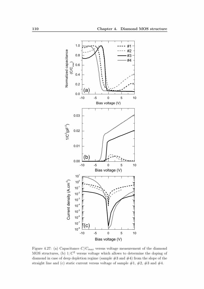
110 Chapter 4. Diamond MOS structure
Figure 4.27: (a) Capacitance C/Cmax versus voltage measurement of the diamond
MOS structures, (b) 1/C2 versus voltage which allows to determine the doping of
diamond in case of deep depletion regime (sample #3 and #4) from the slope of the
straight line and (c) static current versus voltage of sample #1, #2, #3 and #4.
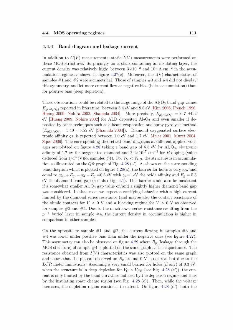
4.4. MOS operating regimes 111
4.4.4 Band diagram and leakage current
In addition to C(V ) measurements, static I(V ) measurements were performed on
these MOS structures. Surprisingly for a stack containing an insulating layer, the
current density was relatively high: between 310−2 and 101 A.cm−2 in the accu-
mulation regime as shown in figure 4.27(c). Moreover, the I(V) characteristics of
samples #1 and #2 were symmetrical. Those of samples #3 and #4 did not display
this symmetry, and let more current flow at negative bias (holes accumulation) than
for positive bias (deep depletion).
These observations could be related to the large range of the Al2O3 band gap values
Eg(Al2O3) reported in literature: between 5.4 eV and 8.8 eV [Kim 2006, French 1990,
Huang 2009, Nohira 2002, Shamala 2004]. More precisely, Eg(Al2O3) = 6.7 ±0.2
eV [Huang 2009, Nohira 2002] for ALD deposited Al2O3 and even smaller if de-
posited by other techniques such as e-beam evaporation and spray pyrolysis method
(Eg(Al2O3) =5.40 - 5.55 eV [Shamala 2004]). Diamond oxygenated surface elec-
tronic affinity qχ is reported between 1.0 eV and 1.7 eV [Maier 2001, Muret 2004,
Sque 2006]. The corresponding theoretical band diagrams at different applied volt-
ages are plotted on figure 4.28 taking a band gap of 6.5 eV for Al2O3, electronic
affinity of 1.7 eV for oxygenated diamond and 2.21017 cm−3 for B-doping (value
deduced from 1/C2(V)for samples #4). For VG < VFB, the structure is in accumula-
tion as illustrated on the QΨ graph of Fig. 4.28 (a’). As shown on the corresponding
band diagram which is plotted on figure 4.28(a), the barrier for holes is very low and
equal to qχi +Egi − qχ−Eg =0.3 eV with χi=1 eV the oxide affinity and Eg = 5.5
eV the diamond band gap (see also Fig. 4.1). This barrier could also be inexistent
if a somewhat smaller Al2O3 gap value or/and a slightly higher diamond band gap
was considered. In that case, we expect a rectifying behavior with a high current
limited by the diamond series resistance (and maybe also the contact resistance of
the ohmic contact) for V < 0 V and a blocking regime for V > 0 V as observed
for samples #3 and #4. Due to the much lower series resistance resulting from the
p++ buried layer in sample #4, the current density in accumulation is higher in
comparison to other samples.
On the opposite to sample #1 and #2, the current flowing in samples #3 and
#4 was lower under positive bias than under the negative ones (see figure 4.27).
This asymmetry can also be observed on figure 4.29 where Rp (leakage through the
MOS structure) of sample #4 is plotted on the same graph as the capacitance. The
resistance obtained from I(V ) characteristics was also plotted on the same graph
and shows that the plateau observed on Rp around 0 V is not real but due to the
LCR meter limitations. Assuming a very small barrier for holes (if any) of 0.3 eV,
when the structure is in deep depletion for VG > VFB (see Fig. 4.28 (c’)), the cur-
rent is only limited by the band curvature induced by the depletion regime and thus
by the insulating space charge region (see Fig. 4.28 (c)). Then, while the voltage
increases, the depletion region continues to extend. On figure 4.28 (d’), both the

112 Chapter 4. Diamond MOS structure
0 25 50 75 100 125 150-14
-12
-10
-8
-6
-4
-2
0
2
4
6
0 25 50 75 100 125 150-14
-12
-10
-8
-6
-4
-2
0
2
4
6
0 25 50 75 100 125 150-14
-12
-10
-8
-6
-4
-2
0
2
4
6
0 25 50 75 100 125 150-14
-12
-10
-8
-6
-4
-2
0
2
4
6
-10 -5 0 5 100.0
0.2
0.4
0.6
0.8
1.0
-10 -5 0 5 100.0
0.2
0.4
0.6
0.8
1.0
-10 -5 0 5 100.0
0.2
0.4
0.6
0.8
1.0
-10 -5 0 5 100.0
0.2
0.4
0.6
0.8
1.0
-4 -2 0 2 4 6 8 10-750
-500
-250
0
250
500
750
-4 -2 0 2 4 6 8 10-750
-500
-250
0
250
500
750
-4 -2 0 2 4 6 8 10-750
-500
-250
0
250
500
750
-4 -2 0 2 4 6 8 10-750
-500
-250
0
250
500
750
(d)
(c’)
(b’)
(a’)
En
erg
y (
eV
)E
ne
rgy (
eV
)E
ne
rgy (
eV
)
VB
EF
CB
Inversion / deep depletion
Depletion
Flat band
p-type diamondAl2O
3
(d’)
(a)
(b)
(c)
V = 7.5 V
V = 0 V
V = -2.3 V = VFB
Position (nm)
Position (nm)
Position (nm)
En
erg
y (
eV
)
Position (nm)
V = -5 V
Al
Accumulation
EFi
C/C
ox
Voltage (V)
C/C
ox
Voltage (V)
C/C
ox
Voltage (V)
C/C
ox
Voltage (V)
V G
-VFB
= - 5
V
Ψs (V)
QS
C(p
C)
V G-V
FB
= - 2
.3 V
Ψs (V)
QS
C(p
C)
V G-V
FB
= 0 V
Ψs (V)
QS
C(p
C)
Inve
rsio
n
V G
-VFB
= - 7
.5 V
Ψs (V)
QS
C(p
C)
Deep depletion
Figure 4.28: Band diagram and QΨ graph of a theoretical diamond metal oxide com-
posed of an Aluminum metal gate, a 20 nm thick Al2O3 oxide, and a p-type diamond
layer doped at 2.21017 cm−3. An affinity of 1.7 eV for O-terminated diamond and
a gap of 6.5 eV for Al2O3 were chosen. The schematic band diagrams and QΨ graph
are plotted for (a)&(a’) the accumulation regime for V =-5 V, (b)&(b’) the flat band
regime for V =-2.3 V, (c)&(c’) the depletion regime for V =0 V and (d)&(d’) the in-
version regime for V =7.5 V. The insets show the corresponding capacitance versus
voltage measurements (both inversion and deep depletion).
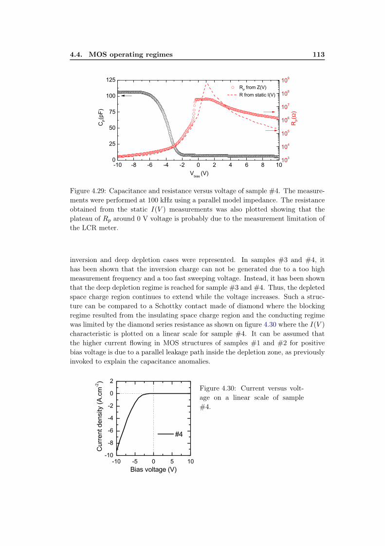
4.4. MOS operating regimes 113
-10 -8 -6 -4 -2 0 2 4 6 8 100
25
50
75
100
125
CP(pF)
Vbias
(V)
103
104
105
106
107
108
109
RP from Z(V)
R from static I(V)
RP(Ω)
Figure 4.29: Capacitance and resistance versus voltage of sample #4. The measure-
ments were performed at 100 kHz using a parallel model impedance. The resistance
obtained from the static I(V ) measurements was also plotted showing that the
plateau of Rp around 0 V voltage is probably due to the measurement limitation of
the LCR meter.
inversion and deep depletion cases were represented. In samples #3 and #4, it
has been shown that the inversion charge can not be generated due to a too high
measurement frequency and a too fast sweeping voltage. Instead, it has been shown
that the deep depletion regime is reached for sample #3 and #4. Thus, the depleted
space charge region continues to extend while the voltage increases. Such a struc-
ture can be compared to a Schottky contact made of diamond where the blocking
regime resulted from the insulating space charge region and the conducting regime
was limited by the diamond series resistance as shown on figure 4.30 where the I(V )
characteristic is plotted on a linear scale for sample #4. It can be assumed that
the higher current flowing in MOS structures of samples #1 and #2 for positive
bias voltage is due to a parallel leakage path inside the depletion zone, as previously
invoked to explain the capacitance anomalies.
-10 -5 0 5 10
-10
-8
-6
-4
-2
0
2
#4
Curr
ent density (
A.c
m-2)
Bias voltage (V)
Figure 4.30: Current versus volt-
age on a linear scale of sample
#4.

114 Chapter 4. Diamond MOS structure
Thanks to the buried p++ layer, the diamond series resistance has been lowered
in sample #4. In addition, the contact resistance of the ohmic contact is expected
to be low thanks to its large area (see picture on figure 4.17) and also to the post
deposition annealing. Thus, assuming that the applied voltage drops only through
the oxide, it is possible to estimate its resistivity in accumulation from the I(V )
characteristics. The current density value can be expressed: J = σE where σ is the
conductivity and E the electric field through the 20 nm of oxide. A conductivity of
210−6 S/cm corresponding to a resistivity of 500 kΩ/cm is found for J=10 A/cm−2
measured at 10 V. This reveals that the oxide has insulating properties (not so good
for an oxide) or/and that a barrier even low exists for holes in accumulation (which
seems observable on the linear I(V ) plot of Fig. 4.30). Furthermore, assuming the
same oxide properties for samples #1 to #4, this result confirms that the current
flowing in samples without buried p++ buried layer is indeed limited by the series
resistance of the p− diamond layer, as previously suggested.
4.4.5 Interface state investigation
The most important challenge to fabricate an efficient MOSFET is to obtain a suffi-
ciently clean oxide/SC interface, in order to reach the inversion regime by avoiding
the Fermi level pinning. Thus the study of the interface states is a crucial step in
the investigation of MOS structures. Nevertheless, some unsolved issues in our MOS
structures will limit such studies. In fact, none of the methods described in section
4.1.3.3 to detect and quantify defects (interface states, charges in the oxide) are
suitable for the diamond MOS structures. For instance, the conductance method is
not applicable because of the high leakage current flowing through the low quality
oxide (see Figure 4.29). Therefore an approach using Terman method to quantify
interfaces states has been considered on sample #4.
Terman method on sample #4
The Terman method [Terman 1962] relies on the hypothesis that the measurement
frequency is high enough to freeze the interface states (i.e. they cannot follow
the a.c signal for capturing or emitting carriers). In that case, only the voltage
sweeping is sufficiently slow to induce a charge or discharge of the interface states.
Thus, the experimental C(V ) of a MOS with interface states is expected to be
different from the theoretical one without interface state. The method is based on
the comparison of these two C(V ) characteristics. Indeed, if we consider again the
equation expressing the neutrality of the charges in a MOS structure (see section
4.1.2.2) by taking this time the charges due to interface states Qis into account, it
writes:
QM +QSC +Qis = 0 (4.24)
Different from the calculation made in section 4.1.2, the charge here are not nor-
malized by the MOS area S. By applying the same line of reasoning than in section
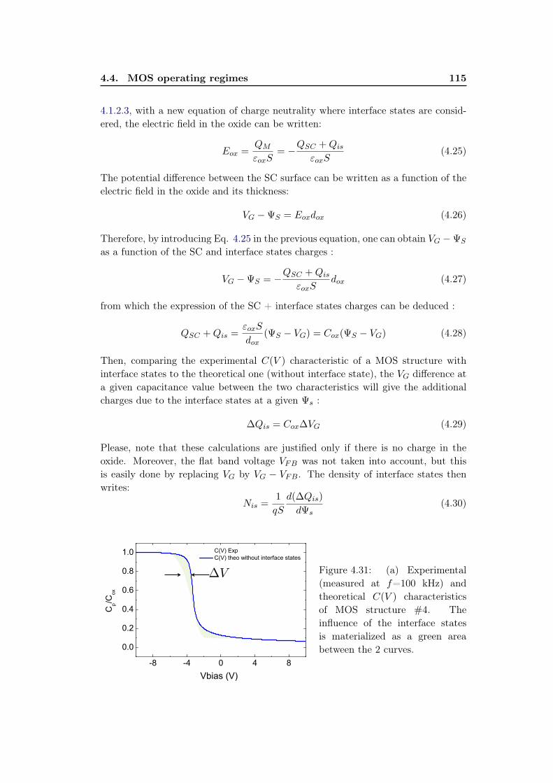
4.4. MOS operating regimes 115
4.1.2.3, with a new equation of charge neutrality where interface states are consid-
ered, the electric field in the oxide can be written:
Eox =QM
εoxS= −QSC +Qis
εoxS(4.25)
The potential difference between the SC surface can be written as a function of the
electric field in the oxide and its thickness:
VG −ΨS = Eoxdox (4.26)
Therefore, by introducing Eq. 4.25 in the previous equation, one can obtain VG −ΨS
as a function of the SC and interface states charges :
VG −ΨS = −QSC +Qis
εoxSdox (4.27)
from which the expression of the SC + interface states charges can be deduced :
QSC +Qis =εoxS
dox(ΨS − VG) = Cox(ΨS − VG) (4.28)
Then, comparing the experimental C(V ) characteristic of a MOS structure with
interface states to the theoretical one (without interface state), the VG difference at
a given capacitance value between the two characteristics will give the additional
charges due to the interface states at a given Ψs :
∆Qis = Cox∆VG (4.29)
Please, note that these calculations are justified only if there is no charge in the
oxide. Moreover, the flat band voltage VFB was not taken into account, but this
is easily done by replacing VG by VG − VFB. The density of interface states then
writes:
Nis =1
qS
d(∆Qis)
dΨs(4.30)
∆V
-8 -4 0 4 8
0.0
0.2
0.4
0.6
0.8
1.0 C(V) Exp
C(V) theo without interface states
Cp/C
ox
Vbias (V)
Figure 4.31: (a) Experimental
(measured at f=100 kHz) and
theoretical C(V ) characteristics
of MOS structure #4. The
influence of the interface states
is materialized as a green area
between the 2 curves.

116 Chapter 4. Diamond MOS structure
The density of interface states was evaluated using this method for sample #4 by
comparing experimental C(V ) characteristics measured at 100 kHz and the theoret-
ical C(V ) characteristics. This last one was obtained using the method described in
section 4.1.3.1. The doping of the SC was obtained from 1/C2 vs V slope of the ex-
perimental data and thickness of the oxide from ellipsometry measurements. These
two characteristics were plotted on figure 4.31. A maximum value of interface states
density was found: 71013 cm−2.eV−1. Unfortunately, the obtained profile of Nis
versus Ψs seems not to be accurate. Indeed several approximations or assumptions
have been done for the calculations :
• although a buried p++ layer was present in this sample, an unexpected fre-
quency dispersion of accumulation capacitance value was still observed (see
Fig. 4.25(b)).
– At 100 kHz, the expected value for accumulation capacitance was mea-
sured. That is why the C(V ) characteristic measured at 100 kHz was
chosen but, there is not any certainty that this frequency is high enough
to "freeze" all the interface states.
– In addition, this experimental C(V ) characteristic was used to determine
the Ψs value needed for calculation. Therefore, it can explain why the
Nis(Ψs) is not relevant.
• Again, due to frequency dispersion, the Cox value measured at 100 kHz was
assumed to be well suited to the calculations (in Eq. 4.29 for instance).
• By using Terman method, it is assumed that there is no charge in the oxide.
This assumption is not realistic for low quality oxides.
These results must therefore be considered with an extreme care and only the order
of magnitude may be significant. For instance, in a working Si MOSFET device, Nis
is about 1010 cm−2.eV−1 or even lower. That is why, after having a demonstrator of
MOS capacitor in diamond, a particular attention must be paid on interface and ox-
ide quality in view of MOSFET fabrication (this work is planned in the framework
of A. Maréchal’s PhD thesis). Moreover, it is hard to distinguish the contribu-
tion of interface states from other possible contributions as mentioned above (series
resistance, deep level in SC, see section 4.4.2.1). Even if it seems contradictory,
a relevant quantification of interface states has to be performed on better quality
MOS structures.
4.4.6 Oxide improvement: sample #6
Sample #6 was fabricated by using the same process than sample #4 (i.e. with a
buried p++ layer to reduce series resistance) except for the Al metal gate thickness
which was reduced from 100 nm to 15 nm in order to be UV semi-transparent. In
fact, this sample has been initially aimed to be tested under UV light (energy larger
than the diamond band gap) in order to create minority carriers by illumination.
4.4. MOS operating regimes 117
4.4.6.1 Optical generation of minority carrier
As previously mentioned, minority carriers can theoretically be generated optically
if the sample is illuminated with an energy larger than the diamond gap (5.47 eV).
This corresponds to a maximum wavelength of:
λ =hc
EG= 227nm (4.31)
where h is the Planck constant and c the light velocity. A deuterium pulsed light
with a broad and continuous spectrum from180 to 370 nm was used. The metal
gate and the oxide should also be transparent so that minority carriers can be
generated under the oxide. That is why on sample #6, only 15 nm of Al as a gate
metal was deposited instead of 100 nm for the other samples. For such low thickness
aluminum should be UV light transparent. The experiments were led under vacuum.
Unfortunately no difference with or without illumination was observed. This could
be due to several facts :
• The stack of 15 nm Al + 20 nm Al2O3 is may not be UV transparent.
• Even if minority carriers were provided by illumination, the frequency used for
measurements (f = 100 kHz) was probably too high for such a high band gap
material. Unfortunately, our LCR meter do not allow us to perform reliable
measurements at frequencies lower than 500 Hz.
4.4.6.2 Frequency dispersion and low frequency measurements
Sample #6 is theoretically similar to sample #4 in term of fabrication recipe, ex-
cept the thickness of the metal gate which is 15 nm instead of 100 nm. Surprisingly,
almost no frequency dispersion of the capacitance value was observed on C(V) char-
acteristics measured in the same frequency range than other samples (from 1 kHz
to 1 MHz, see Fig. 4.32). However, the capacitance value measured in the accu-
mulation regime is about 10 times smaller than the expected value. This value is
nearly the same than the value measured at very high frequency for sample #4 (see
Fig. 4.25) and is also in good agreement with the capacitance value deduced from
the Nyquist plot (see figure 4.12) of sample #2.
We had the opportunity to test during few hours a Solartron equipment which al-
lows very low frequency measurements. Using f = 1 Hz (figure 4.33 (a)), even if the
measurement was quite noisy, the capacitance value in accumulation seemed to be
approximately the one expected for 20 nm of aluminum oxide. Figure 4.33 (b) dis-
plays the 1/C2 versus voltage plot which allows to determine the doping of diamond
in case of deep depletion regime from the slope of the straight line. An effective
doping of 1.71017 cm−3 was obtained in agreement with the diamond growth pro-
cess used (the same than sample #1 which has been analyzed by SIMS, cf. figure
4.26). Using this effective doping value, an oxide thickness of 20 nm and a relative
oxide permittivity value of 7.7, the corresponding theoretical C(V ) characteristics
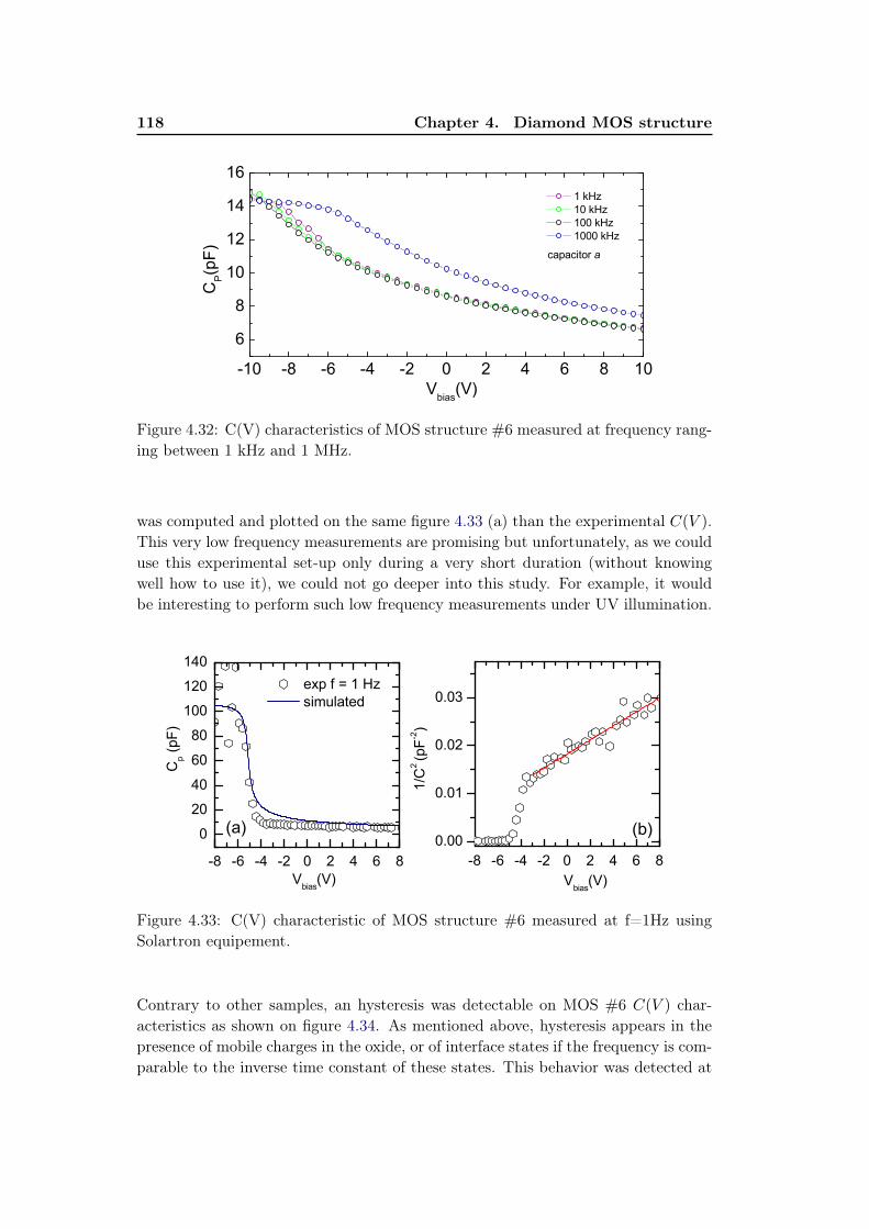
118 Chapter 4. Diamond MOS structure
-10 -8 -6 -4 -2 0 2 4 6 8 10
6
8
10
12
14
16
1 kHz
10 kHz
100 kHz
1000 kHz
CP(p
F)
Vbias
(V)
capacitor a
Figure 4.32: C(V) characteristics of MOS structure #6 measured at frequency rang-
ing between 1 kHz and 1 MHz.
was computed and plotted on the same figure 4.33 (a) than the experimental C(V ).
This very low frequency measurements are promising but unfortunately, as we could
use this experimental set-up only during a very short duration (without knowing
well how to use it), we could not go deeper into this study. For example, it would
be interesting to perform such low frequency measurements under UV illumination.
-8 -6 -4 -2 0 2 4 6 8
0.00
0.01
0.02
0.03
-8 -6 -4 -2 0 2 4 6 8
0
20
40
60
80
100
120
140
(b)
exp f = 1 Hz
simulated
Cp (
pF
)
Vbias
(V)
(a)
Vbias
(V)
1/C
2 (p
F-2)
Figure 4.33: C(V) characteristic of MOS structure #6 measured at f=1Hz using
Solartron equipement.
Contrary to other samples, an hysteresis was detectable on MOS #6 C(V ) char-
acteristics as shown on figure 4.34. As mentioned above, hysteresis appears in the
presence of mobile charges in the oxide, or of interface states if the frequency is com-
parable to the inverse time constant of these states. This behavior was detected at
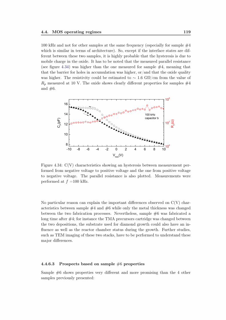
4.4. MOS operating regimes 119
100 kHz and not for other samples at the same frequency (especially for sample #4
which is similar in terms of architecture). So, except if the interface states are dif-
ferent between these two samples, it is highly probable that the hysteresis is due to
mobile charge in the oxide. It has to be noted that the measured parallel resistance
(see figure 4.34) was higher than the one measured for sample #4, meaning that
that the barrier for holes in accumulation was higher, or/and that the oxide quality
was higher. The resistivity could be estimated to 1.6 GΩ/cm from the value of
Rp measured at 10 V. The oxide shows clearly different properties for samples #4
and #6.
-10 -8 -6 -4 -2 0 2 4 6 8 10
8
10
12
14
16
CP(pF)
Vbias
(V)
106
107
108
RP(Ω)
100 kHz
capacitor b
Figure 4.34: C(V) characteristics showing an hysteresis between measurement per-
formed from negative voltage to positive voltage and the one from positive voltage
to negative voltage. The parallel resistance is also plotted. Measurements were
performed at f =100 kHz.
No particular reason can explain the important differences observed on C(V) char-
acteristics between sample #4 and #6 while only the metal thickness was changed
between the two fabrication processes. Nevertheless, sample #6 was fabricated a
long time after #4; for instance the TMA precursors cartridge was changed between
the two depositions, the substrate used for diamond growth could also have an in-
fluence as well as the reactor chamber status during the growth. Further studies,
such as TEM imaging of these two stacks, have to be performed to understand these
major differences.
4.4.6.3 Prospects based on sample #6 properties
Sample #6 shows properties very different and more promising than the 4 other
samples previously presented:

120 Chapter 4. Diamond MOS structure
• almost no frequency dependence of the capacitance value was detected,
• the expected oxide capacitance was measured in accumulation with a low
frequency measurement (f=1Hz),
• an hysteresis was detected which could be due to mobile charges in the oxide,
• a very high parallel resistance value was measured, which may announce a
good insulating behavior of the oxide for a future MOSFET.
All these characteristics are very promising and further measurements, particularly
at low frequencies (f .Hz) must be performed. As almost no frequency dependence
of the capacitance value was detected, this sample is a good candidate for advanced
interface states investigation. Studies using long time measurements or pulsed mea-
surements using a deep level transient spectroscopy set-up were started at the end
of my PhD and are still in progress at the moment.

4.5. Conclusion and outlook for diamond MOSFET 121
4.5 Conclusion and outlook for diamond MOSFET
In this chapter, we demonstrated the fabrication of metal oxide diamond structures
where different regimes are controlled by the gate bias: accumulation of holes, de-
pletion and deep depletion. In accumulation regime (negative voltage), a frequency
dispersion of capacitance value was measured and attributed to the high series resis-
tance of diamond but also to defects involved in non ideal MOS structures. In the
positive voltage range where the inversion or deep depletion (depending on measure-
ment frequency) regimes are expected, a capacitance increase was observed in two
of the samples and has been attributed to a possible inversion regimes allowed by
electrons flowing through diamond layer defects. On the contrary, the observation
of the capacitance decrease attributed to the deep depletion regime in the other
samples is consistent with the high measurement frequency (and the fast sweeping
rate) used, which does not allow generation of any minority carrier. UV illumination
of a sample showing deep depletion, did not lead to the detection of minority car-
riers. The frequency measurement and the bias voltage sweeping rate are certainly
still too high to create inversion, even if minority carriers are optically generated.
Nevertheless, the observation of a deep depletion regime in samples #3, #4 and #6
opens the route for the fabrication of diamond MOSFET.
p+
p-
p+
Source Source
Drain
p+
Source Gate Drain
p-type diamond
n-type n-type
metal
oxide
(a) (b)
n
Figure 4.35: Schematic of (a) an horizontal diamond n-Metal-Oxide-Semiconductor
Field Effect Transistor in its simplest form and (b) a vertical V-shape p-MOSFET
for power applications.
In the case of n-MOSFET (see figure 4.35 (a)), the electrons needed for inversion
will be provided by n-type diamond boxes (source and drain). The gate will insure
the electrostatic control of the channel and so, the on state (inversion) and the off
state of the device. Such a transistor would be normally in off state because of a
channel in depletion regime when no bias is applied to the gate (see band diagram in
Fig.4.28(c)), since the flat band voltage is not strongly negative (VFB −2.4 V in
Fig. 4.28). This case is indeed achieved in samples #1, #2 and #3 as it can be seen
on band C(V) measurements in Fig. 4.27, while the more negative flat band voltage
in sample #4, which might induce weak inversion, deserves future investigations.
122 Chapter 4. Diamond MOS structure
The on state (inversion) is expected to be reached for voltage larger than V 2.5
V. This normally off state would be a great advantage of the diamond MOSFET
over the AlGaN/GaN HEMT which is normally on. Nevertheless, the fabrication of
such a structure (see figure 4.35(a)) is a technological challenge as both n-type and
p-type diamond must be grown on the same sample. Moreover, it has to be noticed
that the planar structure will not be well suited to high voltage application which
will require vertical MOSFET architecture (such as represented on Fig. 4.35 (b))
in order to avoid breakdown between the gate and the drain/source due to oxide
limitations. In a MOSFET, not only the SC/oxide interface quality is a matter of
importance to insure high performances for the transistor but also the pn junctions.
The insulation between source and drain in this off state will be generated by the
depleted space charge region due to the pn junction formed by the n-type boxes
(source and drain) and the p-type layer. Indeed, a leaky pn junction would give
bad off state performances. Particular attention has also to be paid to the oxide.
Electrical measurements enabled us to investigate band offsets of the diamond MOS
structures and show that for samples #1, #2, #3 and #4, only a small barrier for
holes exists, which would be an issue during MOSFET operation. In fact, the oxide
must be more insulating to avoid current flowing between source (or drain) and gate,
otherwise the control of the different states would no be effective. Therefore, future
work on MOS structure have to focus on oxide improvement and defects (interface
states and charges in the oxide) investigations. Some roads that can be followed to
continue the investigations initiated in this work are proposed in the following.
Oxide improvement: The oxide of MOS structure #6 has been significantly im-
proved in terms of insulation (very high parallel resistance). However the hysteresis
detected on C(V ) measurement is a possible evidence of mobile charges in the oxide
which could be hydrogen atoms that have not been pumped out during the process.
Thus, an improvement of the aluminium oxide is probably the next crucial step.
For instance, use of active ozone instead of water precursor would help for instance
to reduce hydrogen contamination in the oxide [Hiraiwa 2012]. Another parameter
which can be tuned is the temperature. In the present study the temperature was
kept low enough to be compatible with the resist used to pattern MOS capacitors.
Therefore, using an approach in which the oxide is deposited on the whole surface
of the sample and then patterned by an etching step could allow to overcome this
limitation and to study the effect of the oxide deposition temperature. One can also
think about an oxide post annealing to desorb unused precursors (including water)
which could be at the origin of mobile charges in the oxide or to crystallize the ox-
ide itself. Finally, the use of other oxides has to be considered i) to obtain a larger
barrier for holes in accumulation and ii) to tune the flat band voltage in such a way
that the MOS structure is in depletion at 0 V to yield a normally off -MOSFET.
Interface states investigation: The almost inexistent frequency dependence of
sample #6 opens the way for more accurate and systematic interface states studies.

4.5. Conclusion and outlook for diamond MOSFET 123
Further measurements, especially using the conductance method, transient capaci-
tance measurements and very low frequencies, must be performed in order to obtain
more reliable quantification of interface states. A multi samples study, where oxide
deposition, surface treatment or diamond growth parameters are varied could help
to distinguish the contribution of interface states from the one of mobile charges in
the oxide (or even defects from the diamond active layer).


Conclusion
As the demand in high power and high frequency electronics keeps increasing, stan-
dard semiconductors, such as silicon, show their limits. Approaches based either
on new architectures or on wide band gap materials should allow to overcome these
limitations. Among these, diamond offers superlative properties such as a wide band
gap, a high breakdown electric field, an outstanding thermal conductivity and high
carriers mobility. Thus, it is foreseen as the ultimate semiconductor that can not
be surpassed by others. Besides, recent progresses in substrate and epilayer growth
allow to consider seriously devices based on diamond semiconductor. Nevertheless,
it also suffers from limitations, especially the difficulty to n-dope and the high ion-
ization energy of the boron p-type dopant that results in a low carrier concentration
at room temperature. Innovative solutions relying on 2D gas or/and field effect ion-
ization have been proposed to overcome this problem. This PhD work was focused
on two of these solutions, which might address different sectors of power electronics.
On one hand, high frequency applications are aimed at using boron doped delta-field
effect transistors involving a thin highly doped layer between two intrinsic layers,
resulting in a conduction combining a high mobility (due to a confinement-induced
delocalisation of carriers away from the ionized impurities) with a large carrier con-
centration (due to metallic behavior). In this work, the growth of nanometric sized
delta-layer using an in-situ etching back technique was demonstrated using SIMS
and TEM analysis and confirmed by electrical measurements. Then, the temper-
ature dependence of electrical properties of several nanometric scaled delta boron
doped layer were investigated experimentally (by Hall effect and four probe mea-
surements) and theoretically over a large temperature range (6 K < T < 500 K).
The samples can be classified in two categories with distinct behaviours:
• Two samples showed an insulating non metallic conduction dominated by a
hopping mechanism with an anomalous exponent of 0.7 which has already
been observed in thin metallic films but is not yet well understood.
• A metallic conduction was found in a wide variety of delta-layer thickness
ranging from less than 2 nm to 40 nm (with sheet carrier from 1014 cm−2
to 51015 cm−2). Surprisingly, the same mobility value of 3±1 cm2/Vs was
measured independently of the delta-layer thickness. Three dimensional and
two dimensional mobility models were considered to explain this phenomenon.
Scattering mechanisms by ionized impurity (3D) was found to be the best
candidate for such low mobility. The model used in this work gives a relative
agreement with this value even if a discrepancy remains. Future works are
needed to fully understand this particular value. An exact calculation will
certainly need a better knowledge of the valence bands (dispersion and/or
boundary with localized states) at energy levels close to the Fermi level of

126 Chapter 4. Diamond MOS structure
such metallic B-doped diamond.
Finally, the thinnest metallic layers (< 2 nm with pS 1014 cm−2) reported in this
work did not exhibit the expected improvement of the mobility (µ=3 cm2/V.s).
The mobility was too low to consider that high frequency diamond delta field effect
transistor are able to compete with existing AlGaN/GaN HEMT showing a mobility
of 2200 cm2/V.s.
On the other hand, high voltage applications are aimed at with metal oxide semi-
conductor field effect transistor (MOSFET) where the conducting or insulating be-
havior of the channel is based on the electrostatic control of the band curvature
at the oxide/semiconducting diamond interface. During this PhD project, metal-
oxide-semiconductor (MOS) structures with aluminium oxide (Al2O3) as insulator
and p−type (100) mono-crystalline diamond as semiconductor were fabricated and
investigated by capacitance versus voltage C(V ) and current versus voltage I(V )
measurements. The aluminum oxide dielectric was deposited using low temperature
atomic layer deposition on an oxygenated diamond surface. The C(V ) measure-
ments demonstrate that accumulation, depletion and deep depletion regimes can be
controlled by the bias voltage. In the accumulation regime, a frequency dispersion of
capacitance value was noticed and has been attributed to the high series resistance
of diamond but also to defects involved in a non ideal MOS structures. A band
diagram was proposed to explain the surprisingly high leakage current flowing in ac-
cumulation regime: the barrier (at the SC/oxide) for holes seems to be very low (0.3 eV). For positive voltage (larger than the threshold voltage) a MOS structure is
expected to be in the inversion regime only if minority carriers could be provided to
the channel. If not, the depletion of the semiconductor will continue until reaching
the deep depletion regime. In the case of diamond which has a very large band gap,
minority carriers could be thermally generated only by using very low measurement
frequency (f n 1 Hz). Thus, the observation of deep depletion regimes in some
samples is in accordance to the measurement frequency used and is indicative of
a sufficiently clean oxide/diamond interface. It therefore opens the route for the
fabrication of a diamond MOSFET in which the electrons will be provided to the
channel by n-type drain and source. Nevertheless, a particular attention has to be
paid to the oxide investigation in order to improve its quality (insulating properties,
barrier for holes) as it will be a key point for the future diamond MOSFET.
Bibliography
[Adkins 1998] C. J. Adkins and E. G. Astrakharchik. Screened hopping conduction
in ultrathin metal films. J. Phys.: Condens. Matter, vol. 10, no. 30, page
6651, August 1998. (Cited on page 61.)
[Aleksov 1999] A Aleksov, A Vescan, M Kunze, P Gluche, W Ebert, E Kohn,
A Bergmeier and G Dollinger. Diamond junction FETs based on delta-doped
channels. Diamond and Related Materials, vol. 8, no. 2–5, pages 941–945,
March 1999. (Cited on page 52.)
[Araùjo 2013] D. Araùjo, M. P. Alegre, J. C. Piñero, A. Fiori, E. Bustarret and
F. Jomard. Boron concentration profiling by high angle annular dark field-
scanning transmission electron microscopy in homoepitaxial delta-doped dia-
mond layers. Appl. Phys. Lett., vol. 103, no. 4, pages 042104–042104–4, July
2013. (Cited on pages 24 and 30.)
[Baliga 1982] B. J. Baliga. Semiconductors for high-voltage, vertical channel field-
effect transistors. Journal of Applied Physics, vol. 53, no. 3, page 1759,
March 1982. (Cited on pages 5 and 8.)
[Baliga 1989] B. Jayant Baliga. Power semiconductor device figure of merit for high-
frequency applications. Electron Device Letters, IEEE, vol. 10, no. 10, pages
455–457, 1989. (Cited on page 8.)
[Balmer 2008] R.S Balmer, I Friel, S.M Woollard, C.J.H Wort, G.A Scarsbrook, S.E
Coe, H El-Hajj, A Kaiser, A Denisenko, E Kohn and J Isberg. Unlocking
diamond’s potential as an electronic material. Philosophical Transactions
of the Royal Society A: Mathematical, Physical and Engineering Sciences,
vol. 366, no. 1863, pages 251 –265, January 2008. (Cited on page 13.)
[Balmer 2013] Richard S. Balmer, Ian Friel, Steven Hepplestone, Jan Isberg,
Michael J. Uren, Matthew L. Markham, Nicola L. Palmer, James Pilkington,
Paul Huggett, Saman Majdi and Richard Lang. Transport behavior of holes
in boron delta-doped diamond structures. J. Appl. Phys., vol. 113, no. 3,
pages 033702–033702–10, January 2013. (Cited on pages 15, 52, 55, 64, 65,
71, 73, 74 and 77.)
[Bergmann 1984] Gerd Bergmann. Weak localization in thin films: a time-of-flight
experiment with conduction electrons. Physics Reports, vol. 107, no. 1, pages
1–58, May 1984. (Cited on page 71.)
[Borst 1995] T.H. Borst and O. Weis. Electrical characterization of homoepitaxial
diamond films doped with B, P, Li and Na during crystal growth. Diamond
and Related Materials, vol. 4, no. 7, pages 948–953, 1995. (Cited on page 11.)

128 Bibliography
[Boukherroub 2005] Rabah Boukherroub, Xavier Wallart, Sabine Szunerits,
Bernadette Marcus, Pierre Bouvier and Michel Mermoux. Photochemical
oxidation of hydrogenated boron-doped diamond surfaces. Electrochemistry
Communications, vol. 7, no. 9, pages 937–940, September 2005. (Cited on
pages 98 and 104.)
[Bousquet 2014] J. Bousquet, G. Chicot, D. Eon and E. Bustarret. Spectroscopic el-
lipsometry of homoepitaxial diamond multilayers and delta-doped structures.
Applied Physics Letters, vol. 104, no. 2, page 021905, January 2014. (Cited
on pages 24 and 68.)
[Cheng 2012] Shaoheng Cheng, Liwen Sang, Meiyong Liao, Jiangwei Liu, Masataka
Imura, Hongdong Li and Yasuo Koide. Integration of high-dielectric constant
Ta2O5 oxides on diamond for power devices. Appl. Phys. Lett., vol. 101,
no. 23, pages 232907–232907–5, December 2012. (Cited on pages 15 and 97.)
[Chicot 2011] Gauthier Chicot, Aurélien Maréchal, Pierre Muret and Julien Pernot.
Procédé de fabrication d’un empilement MOS sur un substrat en diamant.
Patent, December 2011. (Cited on page 97.)
[Chicot 2012] G. Chicot, T. N. Tran Thi, A. Fiori, F. Jomard, E. Gheeraert, E. Bus-
tarret and J. Pernot. Hole transport in boron delta-doped diamond structures.
Appl. Phys. Lett., vol. 101, no. 16, pages 162101–162101–4, October 2012.
(Cited on pages 15, 52 and 55.)
[Chicot 2013] G. Chicot, A. Maréchal, R. Motte, P. Muret, E. Gheeraert and J. Per-
not. Metal oxide semiconductor structure using oxygen-terminated diamond.
Appl. Phys. Lett., vol. 102, no. 24, page 242108, 2013. (Cited on page 97.)
[Chung 2010] J.W. Chung, William E. Hoke, E.M. Chumbes and T. Palacios. Al-
GaN/GaN HEMT With 300-GHz. IEEE Electron Device Letters, vol. 31,
no. 3, pages 195–197, 2010. (Cited on page 15.)
[Davies 1998] J. H. Davies. The physics of low-dimensional semiconductors: an
introduction. Cambridge University Press, Cambridge, U.K. ; New York,
NY, USA, 1998. (Cited on page 69.)
[Deguchi 1996] Masahiro Deguchi, Makoto Kitabatake and Takashi Hirao. Electri-
cal properties of boron-doped diamond films prepared by microwave plasma
chemical vapour deposition. Thin Solid Films, vol. 281-282, pages 267–270,
1996. (Cited on page 11.)
[Edgington 2012] Robert Edgington, Syunsuke Sato, Yuichiro Ishiyama, Richard
Morris, Richard B. Jackman and Hiroshi Kawarada. Growth and electrical
characterisation of 6-doped boron layers on (111) diamond surfaces. J. Appl.
Phys., vol. 111, no. 3, February 2012. WOS:000301029800053. (Cited on
pages 15, 52, 55 and 77.)
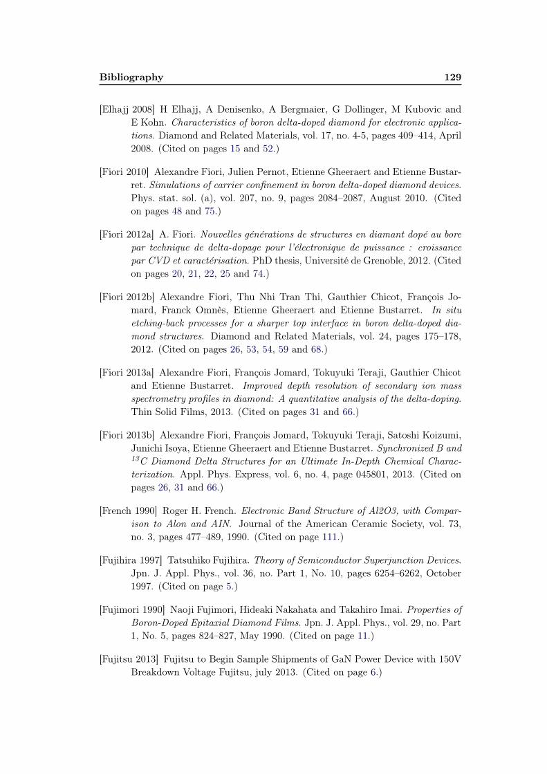
Bibliography 129
[Elhajj 2008] H Elhajj, A Denisenko, A Bergmaier, G Dollinger, M Kubovic and
E Kohn. Characteristics of boron delta-doped diamond for electronic applica-
tions. Diamond and Related Materials, vol. 17, no. 4-5, pages 409–414, April
2008. (Cited on pages 15 and 52.)
[Fiori 2010] Alexandre Fiori, Julien Pernot, Etienne Gheeraert and Etienne Bustar-
ret. Simulations of carrier confinement in boron delta-doped diamond devices.
Phys. stat. sol. (a), vol. 207, no. 9, pages 2084–2087, August 2010. (Cited
on pages 48 and 75.)
[Fiori 2012a] A. Fiori. Nouvelles générations de structures en diamant dopé au bore
par technique de delta-dopage pour l’électronique de puissance : croissance
par CVD et caractérisation. PhD thesis, Université de Grenoble, 2012. (Cited
on pages 20, 21, 22, 25 and 74.)
[Fiori 2012b] Alexandre Fiori, Thu Nhi Tran Thi, Gauthier Chicot, François Jo-
mard, Franck Omnès, Etienne Gheeraert and Etienne Bustarret. In situ
etching-back processes for a sharper top interface in boron delta-doped dia-
mond structures. Diamond and Related Materials, vol. 24, pages 175–178,
2012. (Cited on pages 26, 53, 54, 59 and 68.)
[Fiori 2013a] Alexandre Fiori, François Jomard, Tokuyuki Teraji, Gauthier Chicot
and Etienne Bustarret. Improved depth resolution of secondary ion mass
spectrometry profiles in diamond: A quantitative analysis of the delta-doping.
Thin Solid Films, 2013. (Cited on pages 31 and 66.)
[Fiori 2013b] Alexandre Fiori, François Jomard, Tokuyuki Teraji, Satoshi Koizumi,
Junichi Isoya, Etienne Gheeraert and Etienne Bustarret. Synchronized B and13C Diamond Delta Structures for an Ultimate In-Depth Chemical Charac-
terization. Appl. Phys. Express, vol. 6, no. 4, page 045801, 2013. (Cited on
pages 26, 31 and 66.)
[French 1990] Roger H. French. Electronic Band Structure of Al2O3, with Compar-
ison to Alon and AIN. Journal of the American Ceramic Society, vol. 73,
no. 3, pages 477–489, 1990. (Cited on page 111.)
[Fujihira 1997] Tatsuhiko Fujihira. Theory of Semiconductor Superjunction Devices.
Jpn. J. Appl. Phys., vol. 36, no. Part 1, No. 10, pages 6254–6262, October
1997. (Cited on page 5.)
[Fujimori 1990] Naoji Fujimori, Hideaki Nakahata and Takahiro Imai. Properties of
Boron-Doped Epitaxial Diamond Films. Jpn. J. Appl. Phys., vol. 29, no. Part
1, No. 5, pages 824–827, May 1990. (Cited on page 11.)
[Fujitsu 2013] Fujitsu to Begin Sample Shipments of GaN Power Device with 150V
Breakdown Voltage Fujitsu, july 2013. (Cited on page 6.)

130 Bibliography
[Gabrysch 2008] Markus Gabrysch, Saman Majdi, Anders Hallén, Margareta Lin-
narsson, Adolf Schöner, Daniel Twitchen and Jan Isberg. Compensation in
boron-doped CVD diamond. phys. stat. sol. (a), vol. 205, no. 9, pages 2190–
2194, 2008. (Cited on pages 11, 12 and 73.)
[Gajewski 2009] W. Gajewski, P. Achatz, O. A. Williams, K. Haenen, E. Bustarret,
M. Stutzmann and J. A. Garrido. Electronic and optical properties of boron-
doped nanocrystalline diamond films. Phys. Rev. B, vol. 79, no. 4, page
045206, January 2009. (Cited on page 11.)
[Ghazali 1982] A. Ghazali and J. Serre. Multiple-Scattering Approach to the For-
mation of the Impurity Band in Semiconductors. Phys. Rev. Lett., vol. 48,
no. 13, pages 886–889, March 1982. (Cited on page 60.)
[Gourrier 1983] S. Gourrier and P. Friedel. Caractérisation électrique des états
électroniques d’interfaces isolant/semiconducteur. Acta Electronica, vol. 25,
no. 3, pages 217–240, 1983. (Cited on page 90.)
[Groner 2004] M. D. Groner, F. H. Fabreguette, J. W. Elam and S. M. George.
Low-Temperature Al2O3 Atomic Layer Deposition. Chem. Mater., vol. 16,
no. 4, pages 639–645, 2004. (Cited on pages 103 and 104.)
[H. Ueda 2005] M. Sugimoto H. Ueda. High current operation of GaN power HEMT.
Power Semiconductor Devices and ICs, pages 311 – 314, 2005. (Cited on
page 6.)
[Hiraiwa 2012] Atsushi Hiraiwa, Akira Daicho, Shinichiro Kurihara, Yuki Yokoyama
and Hiroshi Kawarada. Refractory two-dimensional hole gas on hydrogenated
diamond surface. J. Appl. Phys., vol. 112, no. 12, pages 124504–124504–6,
December 2012. (Cited on pages 15, 97 and 122.)
[Hirama 2006] Kazuyuki Hirama, Shingo Miyamoto, Hiroki Matsudaira, Keisaku
Yamada, Hiroshi Kawarada, Toyohiro Chikyo, Hideomi Koinuma, Ken
Hasegawa and Hitoshi Umezawa. Characterization of diamond metal-
insulator-semiconductor field-effect transistors with aluminum oxide gate in-
sulator. Appl. Phys. Lett., vol. 88, no. 11, page 112117, 2006. (Cited on
pages 15, 38 and 97.)
[Hirama 2010] Kazuyuki Hirama, Kyosuke Tsuge, Syunsuke Sato, Tetsuya Tsuno,
Yoshikatsu Jingu, Shintaro Yamauchi and Hiroshi Kawarada. High-
Performance P-Channel Diamond Metal–Oxide–Semiconductor Field-Effect
Transistors on H-Terminated (111) Surface. Appl. Phys. Express, vol. 3,
no. 4, page 044001, March 2010. (Cited on pages 15, 38 and 97.)
[Hoeb 2010] Marco Hoeb, Marianne Auernhammer, Sebastian J. Schoell, Martin S.
Brandt, Jose A. Garrido, Martin Stutzmann and Ian D. Sharp. Thermally
Induced Alkylation of Diamond. Langmuir, vol. 26, no. 24, pages 18862–
18867, December 2010. (Cited on page 98.)

Bibliography 131
[Huang 2008] W. Huang, T.P. Chow, Y. Niiyama, T. Nomura and S. Yoshida. Lat-
eral Implanted RESURF GaN MOSFETs with BV up to 2.5 kV. In 20th
International Symposium on Power Semiconductor Devices and IC’s, 2008.
ISPSD ’08, pages 291–294, 2008. (Cited on page 6.)
[Huang 2009] M. L. Huang, Y. C. Chang, Y. H. Chang, T. D. Lin, J. Kwo and
M. Hong. Energy-band parameters of atomic layer deposited Al2O3 and HfO2
on InxGa1-xAs. Appl. Phys. Lett., vol. 94, no. 5, pages 052106–052106–3,
February 2009. (Cited on pages 80, 97 and 111.)
[Imura 2011] Masataka Imura, Ryoma Hayakawa, Eiichiro Watanabe, Meiyong
Liao, Yasuo Koide and Hiroshi Amano. Demonstration of diamond field ef-
fect transistors by AlN/diamond heterostructure. physica status solidi Rapid
Research Letters, vol. 5, no. 3, pages 125–127, 2011. (Cited on page 15.)
[Johnson 1965] E. Johnson. Physical limitations on frequency and power parameters
of transistors. In IRE International Convention Record, volume 13, pages
27–34, 1965. (Cited on page 7.)
[Kamo 1983] Mutsukazu Kamo, Yoichiro Sato, Seiichiro Matsumoto and Nobuo Se-
taka. Diamond synthesis from gas phase in microwave plasma. Journal of
Crystal Growth, vol. 62, no. 3, pages 642–644, August 1983. (Cited on
page 21.)
[Kasu 2006] M. Kasu, K. Ueda, H. Ye, Y. Yamauchi, S. Sasaki and T. Makimoto.
High RF output power for H-terminated diamond FETs. Diamond and Re-
lated Materials, vol. 15, no. 4–8, pages 783–786, April 2006. (Cited on
page 15.)
[Kasu 2012] Makoto Kasu, Hisashi Sato and Kazuyuki Hirama. Thermal Stabiliza-
tion of Hole Channel on H-Terminated Diamond Surface by Using Atomic-
Layer-Deposited Al2O3 Overlayer and its Electric Properties. Appl. Phys.
Express, vol. 5, no. 2, page 025701, February 2012. (Cited on pages 15, 38
and 97.)
[Kato 2005] Hiromitsu Kato, Satoshi Yamasaki and Hideyo Okushi. n-type doping of
(001)-oriented single-crystalline diamond by phosphorus. Appl. Phys. Lett.,
vol. 86, no. 22, page 222111, May 2005. (Cited on page 10.)
[Kato 2008] Hiromitsu Kato, Hitoshi Umezawa, Norio Tokuda, Daisuke Takeuchi,
Hideyo Okushi and Satoshi Yamasaki. Low specific contact resistance of
heavily phosphorus-doped diamond film. Applied Physics Letters, vol. 93,
no. 20, page 202103, November 2008. (Cited on page 14.)
[Kato 2009] Hiromitsu Kato, Toshiharu Makino, Masahiko Ogura, Norio Tokuda,
Hideyo Okushi and Satoshi Yamasaki. Selective Growth of Buried n+ Dia-
mond on (001) Phosphorus-Doped n-Type Diamond Film. Applied Physics
Express, vol. 2, no. 5, page 055502, 2009. (Cited on page 14.)
132 Bibliography
[Kato 2013] Hiromitsu Kato, Toshiharu Makino, Masahiko Ogura, Daisuke
Takeuchi and Satoshi Yamasaki. Fabrication of bipolar junction transistor on
(001)-oriented diamond by utilizing phosphorus-doped n-type diamond base.
Diamond and Related Materials, vol. 34, pages 41–44, April 2013. (Cited on
page 14.)
[Kawakami 2005] Nobuyuki Kawakami, Yoshihiro Yokota, Takeshi Tachibana,
Kazushi Hayashi and Koji Kobashi. Atomic layer deposition of Al2O3 thin
films on diamond. Diamond and Related Materials, vol. 14, no. 11-12, pages
2015–2018, November 2005. (Cited on pages 15 and 97.)
[Keyes 1972] R.W. Keyes. Figure of merit for semiconductors for high-speed
switches. Proceedings of the IEEE, vol. 60, no. 2, pages 225–225, 1972.
(Cited on page 8.)
[Kim 2006] Hyeong Joon Kim, Sang Yong No, Dail Eom and Cheol Seong Hwang.
Property Improvement of Aluminum-Oxide Thin Films Deposited under Pho-
ton Radiation by Using Atomic Layer Deposition. Journal of the Korean
Physical Society, vol. 49, no. 3, pages 1271–1275, September 2006. (Cited on
page 111.)
[Klein 2007] T. Klein, P. Achatz, J. Kacmarcik, C. Marcenat, F. Gustafsson, J. Mar-
cus, E. Bustarret, J. Pernot, F. Omnes, Bo E. Sernelius, C. Persson, A. Fer-
reira da Silva and C. Cytermann. Metal-insulator transition and supercon-
ductivity in boron-doped diamond. Phys. Rev. B, vol. 75, no. 16, page 165313,
2007. (Cited on pages 11, 56, 59, 66 and 73.)
[Kobayashi 1994] Takeshi Kobayashi, Takuya Ariki, Mamoru Iwabuchi, Tetsuro
Maki, Shozo Shikama and Sei Suzuki. Analytical studies on multiple delta
doping in diamond thin films for efficient hole excitation and conductivity
enhancement. J. Appl. Phys., vol. 76, no. 3, page 1977, 1994. (Cited on
pages 16 and 51.)
[Koizumi 2001] Satoshi Koizumi, Kenji Watanabe, Masataka Hasegawa and Hisao
Kanda. Ultraviolet Emission from a Diamond pn Junction. Science, vol. 292,
no. 5523, pages 1899–1901, June 2001. PMID: 11397942. (Cited on pages 10
and 13.)
[Kramer 1993] B. Kramer and A. MacKinnon. Localization: theory and experiment.
Reports on Progress in Physics, vol. 56, no. 12, page 1469, December 1993.
(Cited on page 61.)
[Kunze 1999] M. Kunze, A. Vescan, G. Dollinger, A. Bergmaier and E. Kohn.
delta-doping in diamond. Carbon, vol. 37, no. 5, pages 787–791, 1999.
WOS:000080216000014. (Cited on page 52.)
[Lagrange 1998] J. P. Lagrange, A. Deneuville and E. Gheeraert. Activation energy
in low compensated homoepitaxial boron-doped diamond films. Diamond and
Bibliography 133
Related Materials, vol. 7, no. 9, pages 1390–1393, September 1998. (Cited
on page 12.)
[Lagrange 1999] J. P. Lagrange, A. Deneuville and E. Gheeraert. A large range of
boron doping with low compensation ratio for homoepitaxial diamond films.
Carbon, vol. 37, no. 5, pages 807–810, 1999. (Cited on pages 11 and 63.)
[Landstrass 1993] M.I. Landstrass, M.A. Plano, M.A. Moreno, S. McWilliams, L.S.
Pan, D.R. Kania and S. Han. Device properties of homoepitaxially grown
diamond. Diamond and Related Materials, vol. 2, no. 5-7, pages 1033–1037,
April 1993. (Cited on page 7.)
[Liu 2012] J. W. Liu, M. Y. Liao, M. Imura and Y. Koide. Band offsets of Al2O3 and
HfO2 oxides deposited by atomic layer deposition technique on hydrogenated
diamond. Appl. Phys. Lett., vol. 101, no. 25, pages 252108–252108–4, De-
cember 2012. (Cited on page 97.)
[Look 1989] D. C Look. Electrical characterization of GaAs materials and devices.
Wiley, Chichester; New York, 1989. (Cited on pages 34 and 72.)
[Look 2008] D. C Look. Two-layer Hall-effect model with arbitrary surface-donor
profiles: application to ZnO. J. Appl. Phys., vol. 104, no. 6, pages 063718–
063718–7, September 2008. (Cited on page 62.)
[Maier 2001] F. Maier, J. Ristein and L. Ley. Electron affinity of plasma-
hydrogenated and chemically oxidized diamond (100) surfaces. Phys. Rev. B,
vol. 64, no. 16, page 165411, October 2001. (Cited on pages 80, 97 and 111.)
[Makino 2008] Toshiharu Makino, Norio Tokuda, Hiromitsu Kato, Shokichi Kanno,
Satoshi Yamasaki and Hideyo Okushi. Electrical and light-emitting properties
of homoepitaxial diamond p–i–n junction. phys. stat. sol. (a), vol. 205, no. 9,
pages 2200–2206, 2008. (Cited on page 13.)
[Makino 2009] Toshiharu Makino, Satoshi Tanimoto, Yusuke Hayashi, Hiromitsu
Kato, Norio Tokuda, Masahiko Ogura, Daisuke Takeuchi, Kazuhiro Oyama,
Hiromichi Ohashi, Hideyo Okushi and Satoshi Yamasaki. Diamond Schottky-
pn diode with high forward current density and fast switching operation. Appl.
Phys. Lett., vol. 94, no. 26, page 262101, June 2009. (Cited on page 13.)
[Marković 2000] N. Marković, C. Christiansen, D. E. Grupp, A. M. Mack,
G. Martinez-Arizala and A. M. Goldman. Anomalous hopping exponents
of ultrathin metal films. Phys. Rev. B, vol. 62, no. 3, pages 2195–2200, July
2000. (Cited on page 61.)
[Mer-Calfati 2014] C. Mer-Calfati, N. Tranchant, P.N. Volpe, F. Jomard, S. Weber,
P. Bergonzo and J.C. Arnault. Sharp interfaces for diamond delta-doping and
SIMS profile modelling. Materials Letters, vol. 115, pages 283–286, January
2014. (Cited on page 26.)
134 Bibliography
[Mitsubishi 2013] Mitsubishi Electric Delivers World’s First SiC
Auxiliary Power Supply Systems for Railcars Mitsubishi.
http://www.mitsubishielectric.com/news/2013/0326-a.html, march 2013.
(Cited on page 6.)
[Mortet 2008] V. Mortet, M. Daenen, T. Teraji, A. Lazea, V. Vorlicek, J. D’Haen,
K. Haenen and M. D’Olieslaeger. Characterization of boron doped diamond
epilayers grown in a NIRIM type reactor. Diamond and Related Materials,
vol. 17, no. 7–10, pages 1330–1334, July 2008. (Cited on pages 11, 12 and 73.)
[Mott 1949] N. F. Mott. The Basis of the Electron Theory of Metals, with Special
Reference to the Transition Metals. Proceedings of the Physical Society.
Section A, vol. 62, no. 7, page 416, July 1949. (Cited on page 51.)
[Muret 2004] Pierre Muret and Christophe Saby. Band bending, electronic affinity
and density of states at several (100) surfaces of boron-doped homoepitaxial
diamond thin films. Semicond. Sci. Technol., vol. 19, no. 1, page 1, January
2004. (Cited on page 111.)
[Muret 2008] Pierre Muret, Julien Pernot, Tokuyuki Teraji and Toshimichi Ito.
Near-Surface Defects in Boron-Doped Diamond Schottky Diodes Studied
From Capacitance Transients. Appl. Phys. Express, vol. 1, no. 3, page
035003, 2008. (Cited on page 106.)
[Muret 2010] Pierre Muret, Julien Pernot, Amit Kumar, Laurence Magaud, Chris-
tine Mer-Calfati and Philippe Bergonzo. Deep hole traps in boron-doped
diamond. Phys. Rev. B, vol. 81, no. 23, page 235205, June 2010. (Cited on
page 106.)
[Muret 2011] P. Muret, P.-N. Volpe, J. Pernot and F. Omnès. Hole traps profile
and physical properties of deep levels in various homoepitaxial diamond films
studied by isothermal and deep level transient spectroscopies. Diamond and
Related Materials, vol. 20, no. 5–6, pages 722–725, May 2011. (Cited on
page 106.)
[Nagakawa 2008] A. Nagakawa, Y. Kawaguchi and K Nakamura. Silicon limit elec-
trical characteristics of power devices and ICs. In ISPS 2008, Prague, 2008.
(Cited on page 4.)
[Naka 2013] Nobuko Naka, Katsuyuki Fukai, Yushi Handa and Ikuko Akimoto. Di-
rect measurement via cyclotron resonance of the carrier effective masses in
pristine diamond. Physical Review B, vol. 88, no. 3, page 035205, July 2013.
(Cited on page 44.)
[Nextnano3 2013] Nextnano3. http://www.nextnano.de/nextnano3/, 2013. (Cited
on page 47.)

Bibliography 135
[Nohira 2002] H. Nohira, W. Tsai, W. Besling, E. Young, J. Petry, T. Conard,
W. Vandervorst, S. De Gendt, M. Heyns, J. Maes and M. Tuominen. Charac-
terization of ALCVD-Al2O3 and ZrO2 layer using X-ray photoelectron spec-
troscopy. Journal of Non-Crystalline Solids, vol. 303, no. 1, pages 83–87,
May 2002. (Cited on pages 80, 97 and 111.)
[Nomura 2008] Takehiko Nomura, Hiroshi Kambayashi, Yuki Niiyama, Shinya
Otomo and Seikoh Yoshida. High-temperature enhancement mode operation
of n-channel GaN MOSFETs on sapphire substrates. Solid-State Electronics,
vol. 52, no. 1, pages 150–155, January 2008. (Cited on page 6.)
[Ohashi 2012] Hiromichi Ohashi. Power devices now and future, strategy of Japan.
In 2012 24th International Symposium on Power Semiconductor Devices and
ICs (ISPSD), pages 9–12, 2012. (Cited on pages 8 and 9.)
[Okano 1989] Ken Okano, Hidetoshi Naruki, Yukio Akiba, Tateki Kurosu,
Masamori Iida, Yoichi Hirose and Terutaro Nakamura. Characterization of
Boron-Doped Diamond Film. Jpn. J. Appl. Phys., vol. 28, no. Part 1, No. 6,
pages 1066–1071, June 1989. (Cited on page 11.)
[Otake 2007] Hirotaka Otake, Shin Egami, Hiroaki Ohta, Yasushi Nanishi and
Hidemi Takasu. GaN-Based Trench Gate Metal Oxide Semiconductor Field
Effect Transistors with Over 100cm2/V.s Channel Mobility. Jpn. J. Appl.
Phys., vol. 46, no. 25, pages L599–L601, 2007. (Cited on page 6.)
[Otake 2008] Hirotaka Otake, Kentaro Chikamatsu, Atsushi Yamaguchi, Tatsuya
Fujishima and Hiroaki Ohta. Vertical GaN-Based Trench Gate Metal Oxide
Semiconductor Field-Effect Transistors on GaN Bulk Substrates. Appl. Phys.
Express, vol. 1, no. 1, page 011105, 2008. (Cited on page 6.)
[Oyama 2009] Kazuihiro Oyama, Sung-Gi Ri, Hiromitsu Kato, Masahiko Ogura,
Toshiharu Makino, Daisuke Takeuchi, Norio Tokuda, Hideyo Okushi and
Satoshi Yamasaki. High performance of diamond p+-i-n+ junction diode
fabricated using heavily doped p+ and n+ layers. Applied Physics Letters,
vol. 94, no. 15, page 152109, April 2009. (Cited on page 14.)
[Oyama 2011] Kazuhiro Oyama, Sung-Gi Ri, Hiromitsu Kato, Daisuke Takeuchi,
Toshiharu Makino, Masahiko Ogura, Norio Tokuda, Hideyo Okushi and
Satoshi Yamasaki. Carrier transport of diamond p+-i-n+ junction diode fab-
ricated using low-resistance hopping p+ and n+ layers. Physica Status Solidi
a-Applications and Materials Science, vol. 208, no. 4, pages 937–942, April
2011. WOS:000289513700034. (Cited on page 14.)
[Pearson 1949] G. L. Pearson and J. Bardeen. Electrical Properties of Pure Sili-
con and Silicon Alloys Containing Boron and Phosphorus. Physical Review,
vol. 75, no. 5, pages 865–883, March 1949. (Cited on pages 11 and 51.)
136 Bibliography
[Pernot 2001] Julien Pernot, W. Zawadzki, S. Contreras, J. L. Robert, E. Neyret
and L. Di Cioccio. Electrical transport in n-type 4H silicon carbide. J. Appl.
Phys., vol. 90, no. 4, pages 1869–1878, 2001. (Cited on page 63.)
[Pernot 2010] J. Pernot, P. N. Volpe, F. Omnès, P. Muret, V. Mortet, K. Haenen
and T. Teraji. Hall hole mobility in boron-doped homoepitaxial diamond.
Phys. Rev. B, vol. 81, no. 20, page 205203, 2010. (Cited on pages 7, 12, 63,
72 and 73.)
[Sato 2000] Toshimaro Sato, Kazutoshi Ohashi, Hiroyuki Sugai, Takashi Sumi, Kat-
suji Haruna, Hiroshi Maeta, Norimasa Matsumoto and Hideo Otsuka. Trans-
port of heavily boron-doped synthetic semiconductor diamond in the hopping
regime. Phys. Rev. B, vol. 61, no. 19, pages 12970–12976, May 2000. (Cited
on page 14.)
[Scharpf 2013] J. Scharpf, A. Denisenko, C. I. Pakes, S. Rubanov, A. Bergmaier,
G. Dollinger, C. Pietzka and E. Kohn. Transport behaviour of boron delta-
doped diamond. Phys. stat. sol. (a), vol. 210, no. 10, pages 2028–2034, 2013.
(Cited on pages 15, 52, 55, 60, 71, 75 and 77.)
[Schroder 2006] Dieter Schroder. Semiconductor material and device characteriza-
tion. IEEE Press; Wiley, [Piscataway NJ] ;Hoboken N.J., 3rd ed. édition,
2006. (Cited on page 90.)
[Schubert 1996] E. F. Schubert. Delta-doping of semiconductors. Cambridge Uni-
versity Press, March 1996. (Cited on pages 16, 45 and 69.)
[Shamala 2004] K.S. Shamala, L.C.S. Murthy and K. Narasimha Rao. Studies on
optical and dielectric properties of Al2O3 thin films prepared by electron beam
evaporation and spray pyrolysis method. Materials Science and Engineering:
B, vol. 106, no. 3, pages 269–274, February 2004. (Cited on page 111.)
[Shklovskii 2008] B. I. Shklovskii. Variable range hopping in thin film with large
dielectric constant. arXiv, no. 0803.3331, March 2008. (Cited on page 61.)
[Soukoulis 1999] C M Soukoulis and E N Economou. Electronic localization in dis-
ordered systems. Waves in Random Media, vol. 9, no. 2, pages 255–269, 1999.
(Cited on page 60.)
[Sque 2006] S. J. Sque, R. Jones and P. R. Briddon. Structure, electronics, and
interaction of hydrogen and oxygen on diamond surfaces. Phys. Rev. B,
vol. 73, no. 8, page 085313, February 2006. (Cited on page 111.)
[Sze 2007] S. M Sze and Kwok Kwok Ng. Physics of semiconductor devices. Wiley-
Interscience, Hoboken, N.J., 2007. (Cited on pages 81 and 85.)
[Tavares 2005] C. Tavares, A. Tajani, C. Baron, F. Jomard, S. Koizumi, E. Gheer-
aert and E. Bustarret. 111-oriented diamond films and p/n junctions grown

Bibliography 137
on B-doped type Ib substrates. Diamond and Related Materials, vol. 14, pages
522–525, 2005. (Cited on page 13.)
[Teraji 2006] T. Teraji, H. Wada, M. Yamamoto, K. Arima and T. Ito. Highly
efficient doping of boron into high-quality homoepitaxial diamond films. Di-
amond and Related Materials, vol. 15, no. 4–8, pages 602–606, April 2006.
(Cited on page 12.)
[Teraji 2008] T. Teraji, S. Koizumi and Y. Koide. Ohmic contact for p-type diamond
without postannealing. Journal of Applied Physics, vol. 104, no. 1, pages
016104–016104–3, July 2008. (Cited on pages 97 and 103.)
[Teraji 2009] T. Teraji, Y. Garino, Y. Koide and T. Ito. Low-leakage p-type di-
amond Schottky diodes prepared using vacuum ultraviolet light/ozone treat-
ment. Journal of Applied Physics, vol. 105, no. 12, pages 126109–126109–3,
June 2009. (Cited on page 97.)
[Terman 1962] L.M. Terman. An investigation of surface states at a silicon/silicon
oxide interface employing metal-oxide-silicon diodes. Solid-State Electronics,
vol. 5, no. 5, pages 285–299, September 1962. (Cited on page 114.)
[Thonke 2003] Klaus Thonke. The boron acceptor in diamond. Semicond. Sci. Tech-
nol., vol. 18, no. 3, pages S20–S26, March 2003. (Cited on pages 11, 12
and 73.)
[Tsukioka 2006] Kunio Tsukioka and Hideyo Okushi. Hall Mobility and Scattering
Mechanism of Holes in Boron-Doped Homoepitaxial Chemical Vapor Depo-
sition Diamond Thin Films. Jpn. J. Appl. Phys., vol. 45, no. 11, pages
8571–8577, 2006. (Cited on pages 11, 12, 61 and 73.)
[Tumilty 2009] Niall Tumilty, Joseph Welch, Richard Lang, Christopher Wort,
Richard Balmer and Richard B. Jackman. An impedance spectroscopic in-
vestigation of the electrical properties of delta-doped diamond structures. J.
Appl. Phys., vol. 106, no. 10, November 2009. WOS:000272932300045. (Cited
on pages 15 and 52.)
[Umezawa 2012] H. Umezawa, M. Nagase, Y. Kato and S. i Shikata. High tempera-
ture application of diamond power device. Diamond and Related Materials,
vol. 24, pages 201–205, 2012. (Cited on page 9.)
[van der Putten 1992] D. van der Putten, J. T. Moonen, H. B. Brom, J. C. M.
Brokken-Zijp and M. A. J. Michels. Evidence for superlocalization on a
fractal network in conductive carbon-black–polymer composites. Phys. Rev.
Lett., vol. 69, no. 3, pages 494–497, July 1992. (Cited on page 61.)
[Van Keuls 1997] F. W. Van Keuls, X. L. Hu, H. W. Jiang and A. J. Dahm. Screen-
ing of the Coulomb interaction in two-dimensional variable-range hopping.
Phys. Rev. B, vol. 56, no. 3, pages 1161–1169, July 1997. (Cited on page 61.)
138 Bibliography
[Vincent 2005] G. Vincent. All the physical and electrical parameters of the MOS
transistor on a single graph (Q-Ψ). The European Physical Journal - Applied
Physics, vol. 32, no. 03, pages 155–158, 2005. (Cited on pages 83 and 85.)
[Vincent 2008] Gilbert Vincent. Metal oxide semiconductor structure and transistor
behaviour using a single and simple graph (Q-Ψ) which takes into account all
the physical and electrical parameters. J. Appl. Phys., vol. 103, no. 7, page
074505, 2008. (Cited on pages 83 and 87.)
[Visser 1992] E P Visser, G J Bauhuis, G Janssen, W Vollenberg, J P van Enckevort
and L J Giling. Electrical conduction in homoepitaxial, boron-doped diamond
films. J. Phys.: Condens. Matter, vol. 4, no. 36, pages 7365–7376, September
1992. (Cited on page 11.)
[Volpe 2009] Pierre-Nicolas Volpe, Julien Pernot, Pierre Muret and Franck Omnès.
High hole mobility in boron doped diamond for power device applications.
Appl. Phys. Lett., vol. 94, no. 9, pages 092102–092102–3, March 2009. (Cited
on pages 11, 12, 20, 24, 53, 63 and 64.)
[Volpe 2010] Pierre-Nicolas Volpe, Pierre Muret, Julien Pernot, Franck Omnès,
Tokuyuki Teraji, Yasuo Koide, François Jomard, Dominique Planson, Pierre
Brosselard, Nicolas Dheilly, Bertrand Vergne and Sigo Scharnholz. Extreme
dielectric strength in boron doped homoepitaxial diamond. Appl. Phys. Lett.,
vol. 97, no. 22, page 223501, November 2010. (Cited on pages 7 and 14.)
[Volpe 2012a] P. N. Volpe, N. Tranchant, J. C. Arnault, S. Saada, F. Jomard and
P. Bergonzo. Ultra-sharp boron interfaces for delta doped diamond structures.
Phys. stat. solidi rrl, vol. 6, no. 2, pages 59–61, 2012. (Cited on page 54.)
[Volpe 2012b] Pierre-Nicolas Volpe, Jean-Charles Arnault, Nicolas Tranchant, Gau-
thier Chicot, Julien Pernot, François Jomard and Philippe Bergonzo. Boron
incorporation issues in diamond when TMB is used as precursor: Toward ex-
treme doping levels. Diamond and Related Materials, vol. 22, pages 136–141,
2012. (Cited on pages 25, 40 and 53.)
[Walukiewicz 1985] Wladyslaw Walukiewicz. Hole mobility in modulation-doped het-
erostructures: GaAs-AlGaAs. Phys. Rev. B, vol. 31, no. 8, pages 5557–5560,
April 1985. (Cited on page 69.)
[Walukiewicz 1986] W. Walukiewicz. Hole-scattering mechanisms in modulation-
doped heterostructures. J. Appl. Phys., vol. 59, no. 10, page 3577, May 1986.
(Cited on page 69.)
[Werner 1997] M. Werner, R. Locher, W. Kohly, D.S. Holmes, S. Klose and H.J.
Fecht. The diamond Irvin curve. Diamond and Related Materials, vol. 6,
no. 2–4, pages 308–313, March 1997. (Cited on pages 11, 12, 59, 72 and 73.)

Bibliography 139
[Willatzen 1994] M. Willatzen, M. Cardona and N. E. Christensen. Linear muffin-
tin-orbital and k p calculations of effective masses and band structure of
semiconducting diamond. Phys. Rev. B, vol. 50, no. 24, pages 18054–18059,
December 1994. (Cited on page 44.)
[Windheim 1993] J. A. Windheim, V. Venkatesan, D. M. Malta and K. Das. Electri-
cal characterization of semiconducting diamond thin films and single crystals.
Journal of Electronic Materials, vol. 22, no. 4, pages 391–398, April 1993.
(Cited on page 11.)
[Yang 1999] K. J Yang and Chenming Hu. MOS capacitance measurements for high-
leakage thin dielectrics. Electron Device, IEEE Transactions, vol. 46, no. 7,
pages 1500–1501, July 1999. (Cited on page 105.)
[Yoshida 2006] S. Yoshida, Jiang Li, H. Takehara, H. Kambayashi and N. Ikeda.
Fabrication of AlGaN/GaN HFET with a high breakdown voltage of over
1050 V. In IEEE International Symposium on Power Semiconductor Devices
and IC’s, 2006. ISPSD 2006, pages 1–4, 2006. (Cited on page 6.)


Publications

Metal oxide semiconductor structure using oxygen-terminated diamond
G. Chicot,1,a) A. Mar!echal,1 R. Motte,1 P. Muret,1 E. Gheeraert,1 and J. Pernot1,2,b)1Institut N!eel, CNRS and Universit!e Joseph Fourier, BP166, 38042 Grenoble Cedex 9, France2Institut Universitaire de France, 103 boulevard Saint Michel, 75005 Paris, France
(Received 10 April 2013; accepted 5 June 2013; published online 19 June 2013)
Metal-oxide-semiconductor structures with aluminum oxide as insulator and p-type (100)
mono-crystalline diamond as semiconductor have been fabricated and investigated by
capacitance versus voltage and current versus voltage measurements. The aluminum oxide
dielectric was deposited using low temperature atomic layer deposition on an oxygenated
diamond surface. The capacitance voltage measurements demonstrate that accumulation,
depletion, and deep depletion regimes can be controlled by the bias voltage, opening the route for
diamond metal-oxide-semiconductor field effect transistor. A band diagram is proposed and
discussed.VC 2013 AIP Publishing LLC. [http://dx.doi.org/10.1063/1.4811668]
The high breakdown electric field, the elevated mobility,
and the outstanding thermal conductivity make diamond the
ultimate semiconductor for high power and high frequency
applications. Intensive works and important progresses have
been done recently in the field of substrate fabrication, epi-
layer growth, and doping control, but the main problem to
make efficient power devices is the large ionization energies
of the acceptor and donor impurities: 380meV for the boron
acceptor and 570meV for the phosphorus donor. The ioniza-
tion rate of dopants at room temperature is low and the
resulting high series resistance of the active layer is not com-
patible with some device operation (like metal semiconduc-
tor field effect transistor (MESFET), bipolar junction
transistor (BJT), or junction field effect transistor (JFET)).
In order to overcome this problem, solutions based on
two dimensional (2-D) hole gas are under investigation: (i)
H-terminated diamond field effect transistor (FET) using
hole accumulation layer.1–3 Such transistors demonstrate
high frequency operation but deteriorate under high tempera-
ture conditions. (ii) Boron d-FET consisting on a thin heavily
doped (metallic) layer between two intrinsic layers resulting
theoretically in high mobility (due to delocalisation of carrier
away from ionized impurities induced by confinement).
However, obtaining a very thin layer4 (<2 nm needed) is a
technological challenge. Delta layers thinner than 2 nm are
reported5 but did show neither quantum confinement nor
enhancement of the mobility, which is yet too low for high
frequency applications. (iii) Diamond/nitride heterojunctions
FET6 has been recently proposed and their electronic proper-
ties are under investigation at this moment. Concerning more
conventional semiconductor devices, the Si metal oxide
semiconductor field effect transistor (MOSFET) is ubiqui-
tous in digital and analog integrated electronic systems. The
conducting or insulating behavior of the MOSFET is based
on the electrostatic control of the band curvature at the
oxide/semiconductor interface. Unfortunately, the physical
properties of Si semiconductor do not allow to build efficient
MOSFET for power electronics applications (generally insu-
lated gate bipolar transistor is preferred but also limited to
4 kV). MOSFET based on other semiconductors, like III-V
compounds or SiC, are progressing but the performances of
such devices are not competitive with Si devices and anyway
will be always lower than that expected for diamond based
MOSFET.7 The main problem to fabricate a MOS structure
is to achieve the semiconductor oxide interface with a suffi-
ciently low interface states density. In that case, the different
regimes of the MOS can be controlled: accumulation of
majority carriers, depletion, deep depletion, or inversion of
carrier (minority carrier density larger than majority carrier
density at the interface). In most cases and contrary to the
Si/Oxide interface, the too large density of interface states
within the gap are charging under bias voltage, and the
breakdown field of the oxide is reached before deep deple-
tion or inversion regimes. Also, previous MOS structures
performed on diamond1–3,8 exhibited accumulation regime
but no deep depletion or inversion regimes. Recent works
reported investigation of Al2O3 deposited by Atomic Layer
Deposition (ALD) on hydrogen-terminated diamond to
stabilize9 or to study the band offsets10 related to the
hydrogen 2-D gas. MOS structures on diamond using high
dielectric constant Ta2O5 oxides were also reported11 but
did not show the deep depletion regime. In our case, in
order to reach deep depletion or inversion regimes at the
interface of Al2O3/diamond, we introduce an approach
combining an oxygen-terminated diamond with low tem-
perature ALD.12,13 Using this process, we demonstrate that
such MOS capacitor can undergo accumulation, depletion,
and deep depletion. The control of the interface regimes
reported in this work opens the route for diamond
MOSFET and more generally for diamond based electron-
ics. This letter is organized as follows: the first part
describes the experimental details and the diamond MOS
fabrication using ALD technique for oxide deposition. In
the second part, the capacitance measurements are detailed
and analyzed in terms of control of the different regimes
using the gate metal electrode.
The five structures investigated in this work consist of a
stack of Al/Al2O3 gate electrode deposited on a boron-doped
epitaxial diamond layer grown in a microwave plasma
assisted chemical vapor deposition (MPCVD) reactor on Ib
high pressure high temperature (HPHT) (100) diamond
a)Electronic mail: [email protected])Electronic mail: [email protected]
0003-6951/2013/102(24)/242108/5/$30.00 VC 2013 AIP Publishing LLC102, 242108-1
APPLIED PHYSICS LETTERS 102, 242108 (2013)
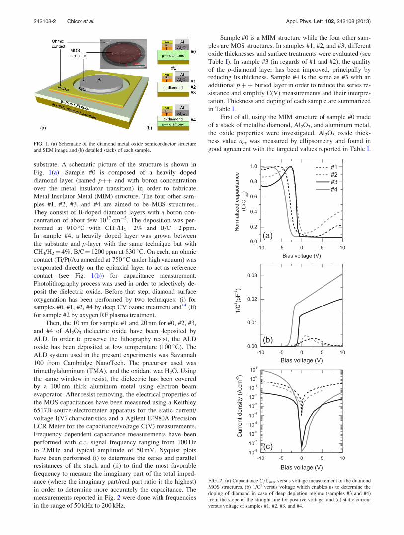
substrate. A schematic picture of the structure is shown in
Fig. 1(a). Sample #0 is composed of a heavily doped
diamond layer (named pþþ and with boron concentration
over the metal insulator transition) in order to fabricate
Metal Insulator Metal (MIM) structure. The four other sam-
ples #1, #2, #3, and #4 are aimed to be MOS structures.
They consist of B-doped diamond layers with a boron con-
centration of about few 1017 cm"3. The deposition was per-
formed at 910 #C with CH4/H2¼ 2% and B/C¼ 2 ppm.
In sample #4, a heavily doped layer was grown between
the substrate and p-layer with the same technique but with
CH4/H2¼ 4%, B/C¼ 1200 ppm at 830 #C. On each, an ohmic
contact (Ti/Pt/Au annealed at 750 #C under high vacuum) was
evaporated directly on the epitaxial layer to act as reference
contact (see Fig. 1(b)) for capacitance measurement.
Photolithography process was used in order to selectively de-
posit the dielectric oxide. Before that step, diamond surface
oxygenation has been performed by two techniques: (i) for
samples #0, #1, #3, #4 by deep UV ozone treatment and14 (ii)
for sample #2 by oxygen RF plasma treatment.
Then, the 10 nm for sample #1 and 20 nm for #0, #2, #3,
and #4 of Al2O3 dielectric oxide have been deposited by
ALD. In order to preserve the lithography resist, the ALD
oxide has been deposited at low temperature (100 #C). The
ALD system used in the present experiments was Savannah
100 from Cambridge NanoTech. The precursor used was
trimethylaluminum (TMA), and the oxidant was H2O. Using
the same window in resist, the dielectric has been covered
by a 100 nm thick aluminum metal using electron beam
evaporator. After resist removing, the electrical properties of
the MOS capacitances have been measured using a Keithley
6517B source-electrometer apparatus for the static current/
voltage I(V) characteristics and a Agilent E4980A Precision
LCR Meter for the capacitance/voltage C(V) measurements.
Frequency dependent capacitance measurements have been
performed with a.c. signal frequency ranging from 100Hz
to 2MHz and typical amplitude of 50mV. Nyquist plots
have been performed (i) to determine the series and parallel
resistances of the stack and (ii) to find the most favorable
frequency to measure the imaginary part of the total imped-
ance (where the imaginary part/real part ratio is the highest)
in order to determine more accurately the capacitance. The
measurements reported in Fig. 2 were done with frequencies
in the range of 50 kHz to 200 kHz.
Sample #0 is a MIM structure while the four other sam-
ples are MOS structures. In samples #1, #2, and #3, different
oxide thicknesses and surface treatments were evaluated (see
Table I). In sample #3 (in regards of #1 and #2), the quality
of the p-diamond layer has been improved, principally by
reducing its thickness. Sample #4 is the same as #3 with an
additional pþþ buried layer in order to reduce the series re-
sistance and simplify C(V) measurements and their interpre-
tation. Thickness and doping of each sample are summarized
in Table I.
First of all, using the MIM structure of sample #0 made
of a stack of metallic diamond, Al2O3, and aluminum metal,
the oxide properties were investigated. Al2O3 oxide thick-
ness value dox was measured by ellipsometry and found in
good agreement with the targeted values reported in Table I.FIG. 1. (a) Schematic of the diamond metal oxide semiconductor structure
and SEM image and (b) detailed stacks of each sample.
FIG. 2. (a) Capacitance C=Cmax versus voltage measurement of the diamond
MOS structures, (b) 1/C2 versus voltage which enables us to determine the
doping of diamond in case of deep depletion regime (samples #3 and #4)
from the slope of the straight line for positive voltage, and (c) static current
versus voltage of samples #1, #2, #3, and #4.
242108-2 Chicot et al. Appl. Phys. Lett. 102, 242108 (2013)

The capacitance was measured and found to be constant ver-
sus applied voltage (!10V to 10V) and versus frequency
(100Hz to 2MHz). Due to the MIM structure, the resultant
capacitance of this stack is equal to the oxide capacitance
Cox given by
Cox ¼!0!oxS
dox; (1)
where !0 is the vacuum permittivity, !ox is the relative per-
mittivity of the oxide, and S is the MOS capacitor area. The
measured value of capacitance was 20% lower than the value
expected if calculated with the Al2O3 relative permittivity
given in literature12 for similar deposition process (i.e., low
temperature ALD except the Si substrate).
In samples #1 and #2, different regimes can be observed
on C(V) measurements (see Fig. 2(a)). For negative voltage
(V!! 5V for #1 and V!! 3V for #2), the holes accumu-
lation is observed. This regime is characterized by an almost
flat capacitance theoretically equal to that of the oxide capac-
itance Cox (Eq. (1)) because the stack is like a planar capaci-
tance (see Fig. 3(a)) composed of the oxide layer in between
two electrodes (Al and diamond). But experimental capaci-
tances in the accumulation regime take values above or
below Cox according to the measurement frequency. A three
elements circuit has been used to introduce the series resist-
ance effect on the measurement. Indeed, in the ideal case,
the capacitance is considered in parallel to the resistance of
the oxide (leakage current through the oxide) leading to a
two elements circuits. In our structure, the series resistance
of the p-type diamond layer cannot be neglected and must be
considered in series with the two elements impedance. Even
with a two frequency correction method15 applied to this
three element circuits, this frequency dispersion still exists
showing that this unexpected behaviour cannot be exclu-
sively attributed to a non negligible series resistance. An
additional impedance due to interface states or/and deep lev-
els in the diamond layer close to the Al2O3/diamond inter-
face (compensating levels in the first hundred nanometers
under Al2O3/diamond interface in a diamond growth without
oxygen in the gas phase16–18) could be responsible of the
phenomenon. While the voltage increases, a space charge
region begins to appear in the semiconductor (Fig. 3(c)), and
the resultant capacitance is now characteristic of the capaci-
tance measured in accumulation in series with the capaci-
tance of the space charge region resulting in a decrease of
the total capacitance. Then, for voltage increasing in positive
values (V" 3V for #1 and V" 2V for #2), the capacitance
starts to increase again. Usually, an increase in capacitance
in this voltage range is characteristic of the strong inversion
regime where majority carriers type is locally (near oxide/
semiconductor interface) inverted, meaning that electron
concentration at the oxide/diamond interface is larger than
the hole density in p-type diamond region. This regime needs
a minority carriers (here electrons) generation mechanism to
be observed. Minority carriers can be provided by thermal or
optical generation of electron-hole pairs in the neutral part of
the semiconductor but frequency of the a.c signal used to
measured capacitance must be sufficiently low to be compa-
rable to the inverse time constant related to the generation
mechanism (approximate maximum value of 10!20 s!1 for a
mid gap trap level) in order that the charges could follow
this a.c signal. In our case, no optical excitation was used
and the frequency measurement is too high for thermal gen-
eration. Diamond p-layer of these two samples shows a large
amount of defects such as hillocks (due to the large thickness
of the layer), which are generally going through the whole
depth of the layer. A mechanism providing electrons from
neutral regions through these defects up to the oxide/semi-
conductor interface could be responsible of this electron gen-
eration. However, a measurement artifact due to the high
FIG. 3. Band diagram of a theoretical diamond metal oxide at different applied bias voltages with an oxide thickness of 20 nm, a p-type diamond doped at
2.2# 1017 cm!3, an affinity of O-terminated diamond of 1.7 eV, and an Al2O3 gap of 6.5 eV. The schematic band diagrams represent (a) the accumulation re-
gime for V¼!5V, (b) the flat band regime for V¼!2.4V, (c) the depletion regime for V¼ 0V, and (d) the inversion regime for V¼ 7.5V. The inset in each
band diagram shows the corresponding capacitance versus voltage measurements (inversion and deep depletion are both plotted).
TABLE I. Physical properties of metal/oxide/diamond structures.
Samples
Doping
(cm!3)
dB!diamond
(nm)
Surface
treatment
dAl2O3
(nm)
#0 >5# 1020a 50a DUV O3 20a
#1 $3# 1017b 1900b DUV O3 10a
#2 $3# 1017b 1900b O2 plasma 20a
#3 3.6# 1017c 300a DUV O3 20a
#4 2.2# 1017c/> 5# 1020a 300a/150a DUV O3 20a
aEstimated from growth conditions.bEstimated from SIMS measurements.cMeasured by C(V) measurements.
242108-3 Chicot et al. Appl. Phys. Lett. 102, 242108 (2013)
oxide leakage current or an impedance due to deep levels (as
suggested above) cannot be discarded. In order to clarify this
point, samples #3 and #4 were fabricated. Diamond layers
are thinner, contain less defects, and in sample #4 a buried
pþþ layer was added in order to reduce the series resistance
and avoid measurement artifacts. For these two samples, the
hole accumulation (with some frequency dispersion) and
depletion are also observable like in samples #1 and #2, but
instead of increasing again in the positive voltage range, the
capacitance continues to decrease. This decrease is typical of
the deep depletion regime. In fact, the 1/C2 versus voltage
plot (see Fig. 2(b)) in this voltage range ("2V !V! 10V)
is linear and typical of the depletion of an homogeneous
doped semiconductor over the depth. By applying a linear fit
to this part, the effective doping of the p-diamond can be
deduced from the slope for these two samples and are
3.6# 1017 cm"3 for sample #3 and 2.2# 1017 cm"3 for sam-
ple #4. These values are consistent with SIMS measurement
performed on a similar sample where the boron doping level
was measured between 2# 1017 cm"3 and 5# 1017 cm"3
over the whole depth of the layer (1.8 lm). The good agree-
ment between B-density determined by 1/C2 and SIMS con-
firmed that the whole area of the MOS capacitor is active.
Moreover, the observation of a deep depletion regime is con-
sistent with the frequency range used for measurement.
Static I(V) measurements were also performed on these
four MOS structures. Surprisingly for a stack containing an
insulating layer, the current density is quite high as it can be
seen in Fig. 2(c). Moreover, the I(V) characteristics of
samples #1 and #2 are symmetrical while those of samples
#3 and #4 are not with more current flowing in the negative
voltage (holes accumulation) than in positive voltage
(deep depletion). These observations could be related to the
large range of the Al2O3 band gap values Eg reported in liter-
ature: between 5.4 eV and 8.8 eV.19–23 More precisely,
Eg¼ 6.76 0.2 eV (Refs. 19 and 23) for ALD deposited
Al2O3 and even smaller if deposited by other techniques
such as e-beam evaporation and spray pyrolysis method
(Eg¼ 5.40–5.55 eV (Ref. 20)). Diamond oxygenated surface
electronic affinity is reported between 1.0 eV and 1.7 eV
(Refs. 24–26). In Fig. 3, theoretical band diagrams are plot-
ted27 at different applied voltages taking a band gap of
6.5 eV for Al2O3, electronic affinity of 1.7 eV for oxygenated
diamond, and 2.2# 1017 cm"3 for B-doping. As shown, the
barrier for holes is very low (%0.4 eV) and could be inexis-
tent if somewhat a smaller Al2O3 gap value or/and a little bit
higher diamond affinity was considered. In that case, we
expect a rectifier behavior with a high current limited by the
diamond series resistance (and maybe also the contact resist-
ance of the ohmic contact) for V < 0V and a blocking re-
gime for V > 0V as observed for samples #3 and #4. Due to
the much lower series resistance resulting from the pþþ
buried layer in sample #4, the current density in accumula-
tion is higher in comparison to other samples. Moreover, for
samples #3 and #4, the current is lower under positive volt-
age than under the negative ones. Assuming a very small
barrier for holes (if any) when the structure is in deep deple-
tion, the current is only limited by the insulating space
charge region. On the contrary, for samples #1 and #2, the
almost symmetrical current may be due to a parallel leakage
path inside the depletion zone, as previously invoked to
explain the capacitance anomalies.
Two different surface treatments (see Table I: DUV O3
and O2 plasma) to oxidize the diamond surface were tested.
Samples #2 and #3 (different treatments with the same oxide
deposition) show different behaviours, particularly in posi-
tive voltage. But as the crystalline quality of these two sam-
ples is different, no clear conclusion can be drawn about a
possible influence of the surface treatment type.
The observation of a deep depletion regime in samples #3
and #4 opens the route for the fabrication of diamond MOSFET.
In case of an n-MOSFET, the electrons needed to create inver-
sion channel at the interface will be provided by n-type diamond
boxes (source and drain). Such a transistor would be in off state
because of a channel in depletion regime when no bias is applied
to the gate (see band diagram in Fig. 3(c)), since the flat band
voltage is not strongly negative (VFB % "2:4 V in Fig. 3). This
case is indeed achieved in samples #1, #2, and #3 as it can be
seen on C(V) measurements in Fig. 2, while the more negative
flat band voltage in sample #4, which might induce weak inver-
sion, deserves future investigations. The on state (inversion) is
expected to be reached for voltage larger than V % 2:5 V.
In this work, we demonstrated the fabrication of metal ox-
ide diamond structures where different regimes are controlled
by bias voltage: accumulation of holes, depletion, and deep
depletion. The properties of the different samples have been
discussed in order to compare the capacitance increase for posi-
tive applied voltages in two of the samples and the capacitance
decrease induced by the deep depletion regime in two other
ones. Electrical measurements enable us to investigate band
offsets of the diamond MOS structures and show that even if
no barrier exists for holes, a MOSFET using this stack would
be operative since both off and on states could be reached.
The authors would like to thank L. Cagnon, Institut
N!eel, CNRS, for his expertise on ALD technique. Funding
for this project was provided by grants from la R!egion
Rhone-Alpes and from the Laboratoire d’excellence LANEF
in Grenoble No. ANR-10-LABX-51-01.
1K. Hirama, S. Miyamoto, H. Matsudaira, K. Yamada, H. Kawarada, T.
Chikyo, H. Koinuma, K. Hasegawa, and H. Umezawa, Appl. Phys. Lett.
88, 112117 (2006).2K. Hirama, K. Tsuge, S. Sato, T. Tsuno, Y. Jingu, S. Yamauchi, and H.
Kawarada, Appl. Phys. Express 3, 044001 (2010).3M. Kasu, H. Sato, and K. Hirama, Appl. Phys. Express 5, 025701 (2012).4A. Fiori, J. Pernot, E. Gheeraert, and E. Bustarret, Phys. Status Solidi A
207, 2084 (2010).5G. Chicot, T. N. Tran Thi, A. Fiori, F. Jomard, E. Gheeraert, E. Bustarret,
and J. Pernot, Appl. Phys. Lett. 101, 162101 (2012).6M. Imura, R. Hayakawa, E. Watanabe, M. Y. Liao, Y. Koide, and H.
Amano, Phys. Status Solidi RRL 5, 125 (2011).7H. Umezawa, M. Nagase, Y. Kato, and S.-i. Shikata, Diamond Relat.
Mater. 24, 201 (2012).8N. Kawakami, Y. Yokota, T. Tachibana, K. Hayashi, and K. Kobashi,
Diamond Relat. Mater. 14, 2015 (2005).9A. Hiraiwa, A. Daicho, S. Kurihara, Y. Yokoyama, and H. Kawarada,
J. Appl. Phys. 112, 124504 (2012).10J. W. Liu, M. Y. Liao, M. Imura, and Y. Koide, Appl. Phys. Lett. 101,
252108 (2012).11S. Cheng, L. Sang, M. Liao, J. Liu, M. Imura, H. Li, and Y. Koide, Appl.
Phys. Lett. 101, 232907 (2012).12M. D. Groner, F. H. Fabreguette, J. W. Elam, and S. M. George, Chem.
Mater. 16, 639 (2004).
242108-4 Chicot et al. Appl. Phys. Lett. 102, 242108 (2013)

13G. Chicot, A. Mar!echal, P. Muret, and J. Pernot, Patent No. FR2012053026
(20 December 2011).14T. Teraji, S. Koizumi, and Y. Koide, J. Appl. Phys. 104, 016104 (2008).15K. J. Yang and C. Hu, IEEE Trans. Electron Devices 46, 1500 (1999).16P. Muret, J. Pernot, T. Teraji, and T. Ito, Appl. Phys. Express 1, 035003 (2008).17P. Muret, J. Pernot, A. Kumar, L. Magaud, C. Mer-Calfati, and P. Bergonzo,
Phys. Rev. B 81, 235205 (2010).18P. Muret, P.-N. Volpe, J. Pernot, and F. Omnes, Diamond Relat. Mater.
20, 722 (2011).19H. Nohira, W. Tsai, W. Besling, E. Young, J. Petry, T. Conard,
W. Vandervorst, S. De Gendt, M. Heyns, J. Maes, and M. Tuominen,
J. Non-Cryst. Solids 303, 83 (2002).
20K. S. Shamala, L. C. S. Murthy, and K. Narasimha Rao, Mater. Sci.
Eng., B 106, 269 (2004).21H. J. Kim, S. Y. No, D. Eom, and C. S. Hwang, J. Korean Phys. Soc. 49,
1271 (2006).22R. H. French, J. Am. Ceram. Soc. 73, 477 (1990).23M. L. Huang, Y. C. Chang, Y. H. Chang, T. D. Lin, J. Kwo, and M. Hong,
Appl. Phys. Lett. 94, 052106 (2009).24S. J. Sque, R. Jones, and P. R. Briddon, Phys. Rev. B 73, 085313 (2006).25P. Muret and C. Saby, Semicond. Sci. Technol. 19, 1 (2004).26F. Maier, J. Ristein, and L. Ley, Phys. Rev. B 64, 165411 (2001).27R. G. Southwick, A. Sup, A. Jain, and W. B. Knowlton, IEEE T. Device
Mat. Re. 11, 236 (2011).
242108-5 Chicot et al. Appl. Phys. Lett. 102, 242108 (2013)

Hole transport in boron delta-doped diamond structures
G. Chicot,1,a) T. N. Tran Thi,1 A. Fiori,1 F. Jomard,2 E. Gheeraert,1 E. Bustarret,1
and J. Pernot11Institut N!eel, CNRS and Universit!e Joseph Fourier, BP166, 38042 Grenoble Cedex 9, France2Groupe d’ !Etude de la Matiere Condens!ee (GEMaC), UMR 8635 du CNRS, UVSQ, 45 Avenue des !Etats-Unis,78035 Versailles Cedex, France
(Received 1 September 2012; accepted 1 October 2012; published online 15 October 2012)
The temperature dependence of the hole sheet density and mobility of four capped delta boron
doped [100]-oriented epilayers has been investigated experimentally and theoretically over a large
temperature range (6K < T < 500K). The influence of the parallel conduction through the thick
buffer layer overgrown on the diamond substrate was shown not to be negligible near room
temperature. This could lead to erroneous estimates of the hole mobility in the delta layer. None of
the delta-layers studied showed any quantum confinement enhancement of the mobility, even the
one which was thinner than 2 nm.VC 2012 American Institute of Physics.
[http://dx.doi.org/10.1063/1.4758994]
Due to outstanding physical properties (large carrier mo-
bility, high breakdown voltage, and exceptional thermal con-
ductivity), diamond is the ultimate semiconductor for high
power and high frequency applications. These features
should in principle allow to develop new low loss electric
switches.1 However, because of the high ionization energy
of the boron p-type dopant,2,3 the equilibrium carrier concen-
tration is low at room temperature, and thus the on-state re-
sistivity is very high. It has been proposed to overcome this
problem by using boron d-doping,4,5 i.e., a highly doped
layer (metallic ½B" # 5$ 1020 cm%3) stacked between two
intrinsic layers, resulting in a conduction combining a high
mobility (due to a confinement-induced delocalisation of car-
riers away from the ionized impurities) with a large carrier
concentration (due to metallic behavior). Recently, several
groups reported fabrication and electrical measurements of
such structures. Most of the electronic properties (sheet den-
sity and mobility) of the d structures have been characterized
by means of a field effect transistor (FET).6,7 Temperature
dependent impedance spectroscopy measurements have been
recently performed to identify the different conduction paths
in the stacked structures.8,9 Hall effect combined to four
probes resistivity measurements have also been used to mea-
sure the sheet density (pS) and the carrier mobility (lH).9,10
The most recent of these works reported a low sheet density
(pS ’ 1013 cm%2) and a hole mobility (lH ¼ 13 cm%2=V ' s)larger than the one expected for highly doped diamond at
room temperature in d-structures on [111]-oriented diamond
substrates.9 Unfortunately, no temperature dependence of pSand lH in d structures has been reported so far. It will be
shown in this work that the analysis of the temperature de-
pendence of pSðTÞ and lHðTÞ is essential in order to distin-
guish the contribution of each conduction path (buffer/high
B-doped layer/cap layer) to the measured (mixed) conductiv-
ity. A correct analysis of the apparent Hall mobility and
sheet density is expected to yield the real hole mobility in
the d-layer or at its interfaces.
The aim of this work was to investigate and describe the
temperature dependence of the electrical transport properties
of thin B-doped diamond embedded between non intention-
ally doped diamond layers in order to evaluate reliably the
carrier mobility and density in the 2D hole gas. In the first
part, a brief description of the samples fabrication and details
about transport experiments will be given. In the second
part, the temperature dependence of the hole sheet density
and mobility will be described and analyzed. Finally, it will
be shown that a d-doped layer thinner than 2 nm has been
grown and that no mobility enhancement, due to quantum
confinement of the holes, was observed.
Four boron doped samples were grown by microwave
plasma-enhanced chemical vapor deposition (MPCVD) on
Ib-type [100]-oriented 3$ 3mm2 diamond substrates (pur-
chased from Sumitomo Electric) and consisting of a highly
p-doped (½B" # 5$ 1020 cm%3) layer of thickness lower than
35 nm grown on a thick non intentionally doped (NiD) buffer
layer suited for high mobility transport3 and covered by
another thin NiD cap layer (from 30 to 65 nm) with similar
nominal properties. The buffer layer was grown in a
CH4=O2=H2 mixture (1%, 0.25%, 0.9875 molar) for 20min
(80 for sample #1). In the case of sample #1, the heavily
doped layer was grown in a CH4=B2H6=H2 mixture (4%,
1500 ppm, 0.96M), then etched ex situ in a H2=O2 plasma,
and then a thin non intentionally cap layer was slowly over-
grown. The heavily doped delta layer of the 3 other samples
were grown in a more diluted CH4=B2H6=H2 mixture (0.5%,
6000 ppm, 0.995M) before being etched in situ in H2=O2
and then covered by a thin cap layer grown in the same gas
mixture as the initial buffer layer. Please note that in this sec-
ond case the plasma was kept on throughout the whole pro-
cess, as described elsewhere.11 The role of the etching step is
to reduce the highly p-doped layer thickness and to improve
the B-doping profile sharpness at the top interface of the
highly doped layer (reduce the residual doping in NiD due to
memory effect of the reactor).
Hall bars have been fabricated on each sample in order
to perform Hall effect and four probes resisitivity measure-
ments. The bars were delineated by O2 electron cyclotrona)Electronic mail: [email protected].
0003-6951/2012/101(16)/162101/4/$30.00 VC 2012 American Institute of Physics101, 162101-1
APPLIED PHYSICS LETTERS 101, 162101 (2012)
Downloaded 15 Oct 2012 to 147.173.64.234. Redistribution subject to AIP license or copyright; see http://apl.aip.org/about/rights_and_permissions

resonance plasma etching of the diamond which surrounds
the mesa. Ti/Pt/Au pads have been deposited and then
annealed at 750 !C under vacuum (<10"8 mbar) during
30min in order to obtain ohmic contact. Hall effect measure-
ments were performed under well controlled conditions
between 6K and 500K. Ohmicity of contacts was checked
by I(V) measurement over the whole range of temperature.
Hall effect measurements were carried out with a dc mag-
netic field B (amplitude of 0.8 T) in the standard configura-
tion (i.e., B parallel and j, the current density, perpendicular
to the growth axis [100]).
The samples can be classified in two categories with two
distinct behaviors (shown in Fig. 1 and summarized in Table I).
On one hand, sample #1 shows a two-regime conduction: in the
lowest temperature range (6K < T < 150K), a metallic con-
duction characterized by constant values of the mobility and
the sheet carrier density, and then, above 150K, an increase of
the mobility and a decrease of the density versus temperature
up to 350K. On the other hand, samples #2, #3, and #4 exhibit
a typical metallic conduction (finite conductivity at low tempe-
rature) with a constant carrier density and a low mobility
(1 < lH < 4 cm2=V s) over the whole temperature range.
The two conduction regimes of sample #1 can be
described quantitatively using a multi layer Hall effect model
recently detailed by Look.12 The two-layer Hall effect model
with arbitrary surface dopant profiles12 has been used here to
investigate important characteristics of the d-doped struc-
ture: (i) the influence of the sharpness of the boron acceptor
profile and (ii) the influence of the buffer layer on the total
hole conduction of the structure (conductivity, mobility, and
sheet density). The transition between the maximum of B-
doped (d-layer) and the buffer could provide a second con-
duction channel in the valence band. In order to quantify this
contribution, the carrier density along the whole profile was
calculated using the neutrality equation in the case of Fermi
Dirac statistics,13 including the boron ionization energy dop-
ing dependence of Ref. 14 and the parameters detailed in
Ref. 15. The compensation has been considered negligible in
a first approximation, and the B-profile was taken as the only
input parameter. The mobility associated to each B-doping
level has been evaluated using the empirical procedure
detailed in Ref. 3. Typically, for a 2 nm thick d-layer (thick-
ness of the sheet with a doping level ½B$ ¼ 5& 1020 cm"3)
and a ½B$ profile decreasing within 1 nm by one doping con-
centration decade from the d-layer to the buffer and top
layers, a sheet density (mobility) decrease (increase) of less
than 40% (5%) was evaluated in comparison with the case of
an abrupt profile. For a smooth transition within 10 nm by
doping concentration decade, the sheet carrier density (mo-
bility) at 500K would be 2.5 times lower (2.5 higher) than
the one expected in the case of an abrupt profile. These
orders of magnitude are far from the variations observed in
sample #1. Finally, the second possibility investigated here
is the hole conduction through the buffer layer. Indeed, using
the B concentration measured by secondary ion mass spec-
troscopy SIMS (see Fig. 2, ½B$ ¼ 3& 1016 cm"3), assuming a
typical compensation3 of 1015 cm"3, homogeneously distrib-
uted throughout the 850 nm of the buffer layer (this active
TABLE I. Summary of electrical transport characteristics of the four sam-
ples: Hall mobility and Hall sheet carrier density measured at 6K and 300K
and thickness of cap layer/d-layer/buffer layer (measured by SIMS unless
specified otherwise).
Thickness (nm) pS (cm"2) lH (cm2/V s) pS (cm
"2) lH (cm2/V s)
Sample cap=d=buffer (T¼ 6K) (T¼ 6K) (T¼ 300K) (T¼ 300K)
#1 50/< 8a/900 4:0& 1014 1.3 1:4& 1013 54.6
#2 '30b/<2a/'300b 1:0& 1014 2.8 1:6& 1014 3.3
#3 40/35/290 4:2& 1015 3.1 4:4& 1015 2.9
#4 65/20/320 2:3& 1015 3.1 2:3& 1015 4.4
aMeasured by Hall effect.bEstimated from growth time.
10 100 100010
-1
100
101
102
103
104
(a)
Sample #1
Sample #2
Sample #3
Sample #4
maximum
bulk mobility
Mobility(cm2/Vs)
T (K)10 100 1000
1012
1013
1014
1015
1016
(b)Sheetcarrierdensity(cm-2)
T (K)
FIG. 1. (a) Hall mobility and (b) Hall sheet carrier density versus tempera-
ture of highly doped layers of different thicknesses (from less than 2 nm to
35 nm) grown on a thick non intentionally doped (NiD) buffer and covered
by another thin NiD cap layer investigated using mesa-etched Hall bars. The
symbols are experimental data and the dashed line is the calculated mobility
for uncompensated diamond using the procedure and parameters described
in Ref. 15.
FIG. 2. (a) Secondary ion mass spectroscopy (SIMS) analysis of samples #1,
#3, and #4 with schematic of the layers stack in the insert and (b) a zoom on
d-layer part of SIMS analysis. The arrows on (a) mark the interface between
buffer layer and substrate. On one hand, it is not relevant to determine maxi-
mum doping and doping gradient of sample #1 since SIMS analysis are not
sufficiently sampled for this sample. On the other hand, doping transition
width can be determined for samples #3 and #4 and are, respectively, 4 nm/
dec and 3 nm/dec on top side and 13 nm/dec and 16 nm/dec on back side.
162101-2 Chicot et al. Appl. Phys. Lett. 101, 162101 (2012)
Downloaded 15 Oct 2012 to 147.173.64.234. Redistribution subject to AIP license or copyright; see http://apl.aip.org/about/rights_and_permissions

thickness takes into account the 200 insulating nm related to
the extension of the space charge region in the B-doped layer
resulting from the nitrogen n-type doping of the Ib-type sub-
strate), we calculate the mobility, the sheet density, and the
conductivity temperature dependence of the buffer layer
(dashed lines in Fig. 3). Then, using a T-independent mobil-
ity and sheet carrier concentration for the metallic d-doped
region (dotted lines in Fig. 3, lH ¼ 1:3 cm2=V s and pS¼ 4" 1014 cm#2), we calculated the mixed mobility and
sheet density corresponding to the abrupt junction between
these two layers (full lines in Fig. 3). The resulting simulated
mobility and sheet carrier density are plotted in Fig. 3.
As shown in Fig. 3, calculated values are in agreement
with the experimental data. The observed temperature
dependences were induced by a mixed conduction in both a
thin metallic (highly p-doped) layer and the buffer and top
(NiD) layers allowing higher mobilities. At low tempera-
tures, the metallic layer (d layer) controls completely the
apparent mobility and sheet density, but while the tempera-
ture increased, the dopants of the thick buffer (0:85 lm)
become ionized and the buffer layer contributes to the total
conduction of the structure. The d-layer cannot be considered
alone to describe the experimental data of the structure in the
high temperature range T > 150K. The carriers responsible
of the conduction at high temperature come from the B-
dopant in the buffer and are not due to a delocalisation of the
carrier from the d-layer. The apparent mobility became
closer to the high mobility of the buffer layer at higher tem-
peratures (see Fig. 3(a)), when the sheet carrier density pSdecreases (see Fig. 3(b)) to that of the lightly doped layer
(lower that of the d-layer). Since the rise of the mobility is
counterbalanced by the decrease in pS, the sheet conductivity
does not show a strong variation over the measured tempera-
ture range (not shown). In conclusion, the mobility and sheet
density measured by Hall effect at room temperature are not
relevant to the d-layer in the case of a thick buffer layer. A
temperature dependent measurement is needed in order to
identify the contribution of each layer of the d-doped struc-
ture to the total conduction and so to the apparent mobility.
A way to avoid this problem is to grow a sufficiently thin
buffer layer (active layer thinner than 100 nm for a 2 nm
thick d-doped layer). This is the case of the three samples
studied in the following part.
For samples #2, #3, and #4, the constant sheet carrier
density and mobility measured over the whole range of tem-
perature are typical of metallic conduction. When the metal-
insulator transition (MIT)16 is reached, the Fermi level is no
longer in the forbidden gap but in the valence band, meaning
that all the dopants are ionized over the whole temperature
range. For sample #3, SIMS analysis (cf., Fig. 2) yields a
thickness of 35 nm and a maximum doping level of ½B% ¼ 1
" 1021 cm#3 and 20 nm at ½B% ¼ 1" 1021 for sample #4,
while no SIMS analysis was undertaken on sample #2
because of its expected very low thickness. In fact, as it has
been shown17 particularly in the case of ultra thin highly
doped layers, SIMS analysis is not free of artifacts18 because
of ion mixing doping transition width at NiD=d interfaces is
overestimated, resulting in erroneous values of d thickness
or maximum doping level value.
In order to evaluate reliably the highly p-doped layer
thickness, iso-lines corresponding to the measured value of
sheet carrier density (iso-ps) are plotted in a graph showing
boron concentration versus thickness of the highly p-doped
layer (cf., Fig. 4). For the metallic conduction observed in
the samples under study (i.e., finite conductivity at low tem-
perature), the boron concentration must be at least equal or
larger than 5" 1020 cm#3 (critical boron concentration for
the MIT16). Also, by plotting the sheet carrier density meas-
ured experimentally in a metallic sample, the maximum
thickness of the d-doped layer can be directly read out at the
intercept with the horizontal line corresponding to the critical
concentration of the MIT transition. The isolines of the four
samples of this work are plotted in Fig. 4. This method is not
useful for samples #3 and #4, since the highly doped layer of
these samples are thick enough (more than 20 nm) to be
0 200 40010
-1
100
101
102
103
104
(b)(a)
Mobility(cm2/Vs)
T (K)0 200 400
1010
1011
1012
1013
1014
1015
1016
Sheetcarrierdensity(cm-2)
T (K)
FIG. 3. (a) Hall mobility and (b) Hall sheet carrier density versus tempera-
ture of sample #1. The dashed lines correspond to the calculated values in
the buffer layer with ½B% ¼ 3" 1016 cm#3 (SIMS) and compensation equals
to 1015 cm#3 distributed over the 850 nm active layer. The dotted lines are
the values assumed for the metallic highly doped region (T-independent and
values measured at 5K; lH ¼ 1:3 cm2=Vs and pS ¼ 4" 1014 cm#2). The
full lines correspond to the two layers Hall mobility and sheet density using
a multilayer Hall effect model.
0.1 1 10 10010
20
1021
1022
#2 #1 #4 #3
pS =2x10 15
cm-2
pS =4x10 14
cm-2
pS =10 14
cm-2
Boronconcentration(cm-3)
Thickness (nm)
pS =4x10 15
cm-2
MIT
FIG. 4. Iso-sheet carrier density lines measured by Hall effect plotted on a bo-
ron concentration (cm#3) versus thickness (nm) map. For ½B% & 5" 1020 cm#3,
the conduction is metallic. The intercepts of the lines (boundaries between full
and dashed) with the horizontal line corresponding to the critical concentration
for the MIT give the maximum thickness of the highly doped region where
½B% > 5" 1020 cm#3. The symbols are SIMS data for sample #3 (square) and
sample #4 (star).
162101-3 Chicot et al. Appl. Phys. Lett. 101, 162101 (2012)
Downloaded 15 Oct 2012 to 147.173.64.234. Redistribution subject to AIP license or copyright; see http://apl.aip.org/about/rights_and_permissions

measured accurately by SIMS. The SIMS data (B-doping
and thickness of the d-layer) are reported in Fig. 4 (open
square for sample #3 and open star for sample #4), in good
agreement with the Hall data (pS ¼ 4" 1015 cm#2 for sam-
ple #3 (blue line) and pS ¼ 2" 1015 cm#2 for sample #4 (or-
ange line)) showing a full activation of B-dopants. For
sample #1 (black line), the iso-ps ¼ 4" 1014 cm#2 (value of
sheet carrier density at low temperature) indicates that the
thickness of the highly doped layer is less than 8 nm. By
doing the same way with iso-ps ¼ 1014 cm#2 of sample #2
(red line), the highly p-doped layer is found to be equal or
thinner than 2 nm. Calculations based only on the hole distri-
bution in the V-shape potential suggest that delocalisation
would occur for d under 3 nm.19 The highly p-doped layer of
sample #2 is rather thin, but the mobility measured is around
3 cm2/Vs, which is typically the same than the one measured
in thicker highly p-doped layer like sample #3 (cf., Fig. 1).
The result shows that the strong coulombic scattering
induced by ionized boron atoms and screened by the free
holes (Fermi screening radius about 0.3 nm) in the d-layer
limits the mobility of the free hole in the same way than in a
bulk material. No quantum confinement enhancement of the
mobility is observed for a d with ps ¼ 1014 cm#2 correspond-
ing to a maximum thickness of 2 nm, suggesting that thinner
d-layers or/and with sharper interfaces should be grown (i.e.,
ps < 1014 cm#2).
To summarize, it has been shown that no quantum
confinement enhancement of the mobility was present even
for d thickness of 2 nm using transport measurements to
evaluate mobility, sheet carrier density, and thickness.
Low temperature Hall effect is a useful tool to evaluate the
doping/thickness window. This approach becomes neces-
sary for very thin d-layers for which SIMS data could be
erroneous or when parallel conduction in a thick buffer
layer leads to an apparent mobility enhancement at room
temperature.
The authors would like to thank B. Fernandez (micro-
fabrication) and P. Giroux (growth), Institut N!eel, CNRS, for
their technical support. Funding for this project was provided
by grants from la R!egion Rhone-Alpes, and Agence Natio-
nale de la Recherche under Grant No. ANR-08-0195.
1R. S. Balmer, I. Friel, S. Woollard, C. J. Wort, G. Scarsbrook, S. Coe, H.
El-Hajj, A. Kaiser, A. Denisenko, E. Kohn, and J. Isberg, Philos. Trans. R.
Soc. A 366, 251 (2008).2J. P. Lagrange, A. Deneuville, and E. Gheeraert, Diamond Relat. Mater. 7,
1390 (1998).3P.-N. Volpe, J. Pernot, P. Muret, and F. Omnes, Appl. Phys. Lett. 94,
092102 (2009).4T. Kobayashi, T. Ariki, M. Iwabuchi, T. Maki, S. Shikama, and S. Suzuki,
J. Appl. Phys. 76, 1977 (1994).5E. F. Schubert, Delta-Doping of Semiconductors (Cambridge University
Press, 1996).6H. El-Hajj, A. Denisenko, A. Kaiser, R. S. Balmer, and E. Kohn, Diamond
Relat. Mater. 17, 1259 (2008).7A. Aleksov, A. Vescan, M. Kunze, P. Gluche, W. Ebert, E. Kohn, A. Berg-
meier, and G. Dollinger, Diamond Relat. Mater. 8, 941 (1999).8N. Tumilty, J. Welch, H. Ye, R. S. Balmer, C. Wort, R. Lang, and R. B.
Jackman, Appl. Phys. Lett. 94, 052107 (2009).9R. Edgington, S. Sato, Y. Ishiyama, R. Morris, R. B. Jackman, and H.
Kawarada, J. Appl. Phys. 111, 033710 (2012).10M. Kunze, A. Vescan, G. Dollinger, A. Bergmaier, and E. Kohn, Carbon
37, 787 (1999).11A. Fiori, T. N. Tran Thi, G. Chicot, F. Jomard, F. Omnes, E. Gheeraert,
and E. Bustarret, Diamond Relat. Mater. 24, 175 (2012).12D. C. Look, J. Appl. Phys. 104, 063718 (2008).13J. Pernot, W. Zawadzki, S. Contreras, J. L. Robert, E. Neyret, and L. Di
Cioccio, J. Appl. Phys. 90, 1869 (2001).14J. P. Lagrange, A. Deneuville, and E. Gheeraert, Carbon 37, 807 (1999).15J. Pernot, P. N. Volpe, F. Omnes, P. Muret, V. Mortet, K. Haenen, and T.
Teraji, Phys. Rev. B 81, 205203 (2010).16T. Klein, P. Achatz, J. Kacmarcik, C. Marcenat, F. Gustafsson, J. Marcus,
E. Bustarret, J. Pernot, F. Omnes, B. E. Sernelius, C. Persson, A. F. da
Silva, and C. Cytermann, Phys. Rev. B 75, 165313 (2007).17A. Takano, Y. Homma, Y. Higashi, H. Takenaka, S. Hayashi, K. Goto, M.
Inoue, and R. Shimizu, Appl. Surf. Sci. 203, 294 (2003).18S. Hofmann, Surf. Interface Anal. 30, 228 (2000).19A. Fiori, J. Pernot, E. Gheeraert, and E. Bustarret, Phys. Status Solidi A
207, 2084 (2010).
162101-4 Chicot et al. Appl. Phys. Lett. 101, 162101 (2012)
Downloaded 15 Oct 2012 to 147.173.64.234. Redistribution subject to AIP license or copyright; see http://apl.aip.org/about/rights_and_permissions
Spectroscopic ellipsometry of homoepitaxial diamond multilayersand delta-doped structures
J. Bousquet,1,2 G. Chicot,1,2 D. Eon,1,2 and E. Bustarret1,21Univ. Grenoble Alpes, Inst. NEEL, F-38042 Grenoble, France2CNRS, Inst. NEEL, F-38042 Grenoble, France
(Received 20 October 2013; accepted 28 December 2013; published online 14 January 2014)
The optimization of diamond-based unipolar electronic devices such as pseudo-vertical Schottky
diodes or delta-doped field effect transistors relies in part on the sequential growth of nominally
undoped (p–) and heavily boron doped (pþþ) layers with well-controlled thicknesses and steep
interfaces. Optical ellipsometry offers a swift and contactless method to characterize the thickness,
roughness, and electronic properties of semiconducting and metallic diamond layers. We report
ellipsometric studies carried out on delta-doped structures and other epitaxial multilayers with various
boron concentrations and thicknesses (down to the nanometer range). The results are compared with
Secondary Ion Mass Spectroscopy and transport measurements. VC 2014 AIP Publishing LLC.
[http://dx.doi.org/10.1063/1.4861860]
Spectroscopic ellipsometry has been introduced quite
early on as an efficient way of characterizing the nucleation
and subsequent coalescence and growth of polycrystalline di-
amond on silicon substrates induced by chemical vapor dep-
osition (CVD), either in situ1–7 or ex situ.8–13 The main
ingredients of this approach were the optical transparency of
diamond in the visible range and the sizable difference
between the refractive index of diamond (around 2.4) and
that of the silicon substrate (around 3.5) over this spectral
range.14 In the case of homoepitaxial growth, no such dis-
continuity was expected between film and substrate, so that
equivalent studies have not been published. Actually, in con-
trast to other semiconductors, spectrometric ellipsometry has
not been a popular way to determine optical constants of sin-
gle crystal diamond. Indeed, even in the ultraviolet region,
close to the direct gap, artefacts most probably related to the
surface roughness of the polished crystals may well have
affected the few reported values.15,16
However, at the heavy boron doping levels leading to me-
tallic properties in diamond (above 4" 1020 [B]/cm3 (Ref.
17)), a noticeable change in refractive index has been detected
by reflectance spectroscopy,18 first in the mid-infrared, then
up to the near ultraviolet range.19 As confirmed by other stud-
ies in the far infrared,20 the contribution of free holes was
fairly well described by an additional Drude component to the
pseudo dielectric function of diamond, and the change of re-
fractive index could be evaluated over the whole spectral
range. A consequence of this observation is that stacks of
well-defined metallic (pþþ) and semiconducting (p# or p)
layers are expected to have spectral characteristics in the visi-
ble range that could be measured and simulated as those of
any optical multilayer, providing an access to their respective
thickness and electronic microscopic properties at optical fre-
quencies. Such epitaxial metallic diamond layers of micromet-
ric to nanometric thickness, which have been proposed as
buried electrical contacts for both n/i/p and Schottky
pseudo-vertical devices,21–23 as source and drain in field effect
transistors (FET) or even as a pseudo-channel24 in
delta-doped metal-insulator semiconductor FETs, have been
recently investigated, and new results about their chemical
profiles25–27 or temperature-dependent transport proper-
ties26,28,29 have been published. It is the purpose of the present
letter to show that spectroscopic ellipsometry provides a
time-effective but yet powerful characterization of metallic
layers or alternating p#/pþþ epitaxial diamond multilayers
similar (before patterning) to those involved in the monolithic
devices mentioned above.
To this aim, we have studied the ellipsometric response
of various diamond homoepitaxial stacks, including
uncapped and capped delta-doped structures and two series
of pþþ epilayers where either the thickness or the doping
level were varied. We report the experimental spectra and
their fits with standard model dielectric functions specific to
each epilayer. Thicknesses, optically determined room tem-
perature resistivities, and carrier concentrations will then be
compared with Secondary Ion Mass Spectroscopy (SIMS)
and DC transport measurements.
A TE10 standing microwave field was obtained in a rec-
tangular waveguide of a microwave plasma-assisted CVD
(MPCVD) reactor where the reaction chamber composed of
a quartz tube was positioned at a maximum of the electric
field. The H2 þ CH4 plasma was ignited close to the dia-
mond substrate, which was held at 910 $C for the non inten-
tionally doped p# layers, and at 830 $C for heavily boron
doped (pþþ) growth resulting from adding diborane (B2H6)
to the gas mixture. The total flow rate was kept to 100 sccm
at a pressure of 40 mbar. Three sets of samples were grown,
labeled as “thickness,” “doping,” and “capped.” The
“thickness” series involved pþþ layers where only the
growth duration was changed between 1 and 60min (CH4/H2
molar ratio of 4%, B2H6/CH4 molar ratio 600 ppm) resulting
in epilayers thicknesses ranging from 30 to 1800 nm. The
samples of the “doping” series are pþþ layers about
1 lm-thick where the diborane to methane ratio was varied
between 150 and 6000 ppm leading to solid state concentra-
tions ranging17,30 from 2" 1020 and 2" 1021 [B]/cm3. The
samples of these two series were considered as metallic at
room temperature. The third set involved three samples
where the pþþ layer was overgrown with a p# “cap layer”
(CL). For one sample dubbed “thick stack,” the growth
0003-6951/2014/104(2)/021905/5/$30.00 VC 2014 AIP Publishing LLC104, 021905-1
APPLIED PHYSICS LETTERS 104, 021905 (2014)
This article is copyrighted as indicated in the article. Reuse of AIP content is subject to the terms at: http://scitation.aip.org/termsconditions. Downloaded to IP:
147.173.64.234 On: Tue, 14 Jan 2014 16:23:58

conditions of the pþþ layer were those of the thickness se-
ries, and the resulting pþþ and cap p" epilayer were a few
lm-thick. For the other two samples dubbed “delta 1” and
“delta 2,” the conditions were changed, with CH4/H2 and
B2H6/CH4 molar ratios in the gas phase of 0.5% and 3000
ppm, respectively, while the total pressure was raised to 67
mbar and the total flow rate to 2 slm in order to reduce the
residence time of the gas species. Under these conditions,
the growth rate decreased from typically 30 to 6 nm/min and
much thinner epilayers were grown. Additionally, as
described elsewhere,29,31 O2 þ H2 gas mixtures were used to
etch in situ the ultra-thin pþþ layers down to the required
thickness without turning off the plasma.
Spectroscopic ellipsometry was performed with a J.A.
Woollam M2000 ellipsometer running under the CompleteEase
software. The ellipsometric angles (W, D) defined by the ratio
of the reflection coefficients for electric fields, respectively, par-
allel (p) and perpendicular (s) to the incidence plane
(rp/rs¼ tan(W)eiD) were acquired over the 240–1000nm wave-
length range at a 75$ incidence angle. These data were simu-
lated using a Cauchy model for the optical constants of
diamond in the case of non-intentional doped layers or sub-
strates, and adding a Drude component to UV oscillators for
metallic layers. Contrary to the epitaxial layers, the 0.3 to
0.5mm-thick undoped [100]-oriented diamond substrate (either
type-Ib or type IIa optical grade crystals) was described as an
incoherent optical layer where only the intensities of the multi-
ple reflected beams should be summed (instead of amplitudes).
A random surface roughness parameter (in nm) was also intro-
duced in the simulation, for the top surface only.
To perform Hall effect measurements, the cap and the
delta-doped layers have been delineated by Reactive Ion
Etching to fabricate a Hall bar. Ohmic contacts have been
fabricated by annealing at 750 $C under vacuum (<10"8
mbar) during 30min the Ti/Pt/Au pads. The sheet carrier
density measurements have been carried out at room temper-
ature in vacuum with a DC magnetic field (amplitude of
0.8 T) in the standard configuration (magnetic field parallel
and current density perpendicular to the growth axis [100]).
In some cases, four terminal silver paste resistivity measure-
ments have also been performed.
The metallic layer optical response has been fitted by
adding a Drude component to the interpolated dielectric
function enid of undoped diamond14
e xð Þ ¼ enidðxÞ þ iNe
2s
e0m0m'
x
1" ixs; (1)
with x the wavenumber (or reciprocal wavelength 1/k), N
the free carriers (here holes) concentration, s the scattering
time, e the elementary electron charge, m0 the electron rest
mass and m* the relative effective mass of the holes. Beside
the thickness d of the pþþ layer, and the top surface rough-
ness, the two fit parameters were the relaxation time s and
the N/m* ratio. This simple relaxation time approximation of
a Fermi metal provides a direct access to the optical resistiv-
ity at zero frequency
q xð Þ ¼ q0ð1" ixsÞ ¼m0m
'
Ne2sð1" ixsÞ: (2)
After each fit, beside the overall minimum mean square devi-
ation (MSE), a table was calculated showing the correlation
coefficients (from 0, no correlation, to 1, fully correlated)
between the fit parameters corresponding to the various
layers of the stack (see Table I).
As shown in Fig. 1(a), in the case of an optically thick
pþþ film (no reflected light coming from the back interface)
the spectral dependence of the two ellipsometric angles W
and D was measured and then simulated by the optical
response of a rough semi-infinite medium with a complex
wavelength-dependent pseudodielectric function e(k) or
refractive index n(k)þik(k). A similar approach can be
applied to polished insulating bulk diamond.
In the case of commercial diamond substrates, the fitted
pseudodielectric functions taking their roughness into
account lie close to those deduced from the n and k values
found in a classical handbook,14 which were as usual readily
interpolated over the present spectral range by a Cauchy
law.14 The real part n of the refractive index was found
slightly higher in yellow type Ib substrates grown at high
pressure and high temperature (HPHT) than in optical grade
TABLE I. Correlation table for the fit of both ellipsometric angles measured
on sample delta-1. The influence of strongly correlated parameters (correla-
tion coefficient close to6 1) cannot be disentangled.
d dCL q s
d 1 "0.8 0.1 "0.9
dCL "0.8 1 0.3 0.9
q 0.1 0.3 1 "0.1
s "0.9 0.9 "0.1 1
FIG. 1. (a) Spectral variation of the ellipsometric angles for an optically
thick pþþ diamond layer. (b) Optical indices deduced from (a), compared
with reflectometry measurements and the refractive index of type-Ib
(HPHT) and type-IIa (CVD) diamond substrates.
021905-2 Bousquet et al. Appl. Phys. Lett. 104, 021905 (2014)
This article is copyrighted as indicated in the article. Reuse of AIP content is subject to the terms at: http://scitation.aip.org/termsconditions. Downloaded to IP:
147.173.64.234 On: Tue, 14 Jan 2014 16:23:58

CVD substrates (Fig. 1(b)). This can be explained by the
high density of isolated Nitrogen in the Ib substrates leading
to an optical absorption above 1.7 eV (below 729 nm). In the
case of the thick metallic diamond layer, in order to obtain
satisfactory simulations, it was necessary to add to e(k) of
undoped diamond a Drude component17 parameterized here
by the zero frequency limit q0 of the frequency-dependent
optical resistivity and by the microscopic relaxation time s,
as defined above. The experimental optical constants n and k
are shown in Fig. 1(b) to be very similar to those previously
published for similar films,18 with a real part n becoming sig-
nificantly weaker than in undoped diamond at longer wave-
lengths. This sizable contrast in refractive index (!20% at
1lm wavelength) between insulating (or p!) and metallic
(pþþ) diamond led us to study optically various stacks of p!
and pþþ epilayers.
The first case that comes to mind is that of uncapped
and thin metallic diamond films grown on commercial sub-
strates, similar to those used in superconductivity27 or delta-
doping25,32 studies. The spectral dependence of the ellipso-
metric angles for two such films (“thickness series”) is given
in Figs. 2(a) and 2(b), with best fit simulations of the Fabry-
Perot fringes yielding thicknesses d of 29 nm and 167 nm for
1 and 5min growth times, within 10% of the thicknesses
expected from the nominal deposition rate of 31 nm/min. A
third example is given on Fig. 2(c), that of a “thick stack”
involving a p! layer grown on top of a pþþ layer grown on a
commercial CVD substrate. The amplitude of the fringes is
smaller, mostly because of an increased surface roughness,
but still determined by the contrast in refractive index, which
increases with the wavelength. The thicknesses resulting
from the fit, d¼ 1.5 lm for the pþþ bottom layer, and
dCL¼ 3.8 lm for the top p! cap layer, were also within 10%
of the values expected from previous boron concentration
SIMS and neutron depth profiles.30 Because the present spec-
tral range was limited to 1lm in the infrared, the maximum
thicknesses measurable in this non-destructive way for such
bilayers were dCL¼ 8 lm for the top p! cap layer and
d¼ 2 lm for the underlying pþþ epilayer.
In the case of uncapped metallic diamond epilayers, as
shown in Fig. 3(a), the reliability of the thickness values
deduced from ellipsometry spectra was confirmed over almost
two orders of magnitude for the whole “thickness series.”
Over this series, the q0 value deduced from the best fit for
each of these samples was almost constant. Once multiplied
by the optically determined thickness d, an average optical
sheet resistivity was determined, and compared in Fig. 3(b) to
the DC value measured at room temperature by the 4-terminal
probe method. In both cases the !1 slope of the log-log plot
was compatible with a constant resistivity value over the
whole thickness range. This resistivity value was 2.4mX.cm
for DC measurements, higher than extrapolated from the opti-
cal data (1.7mX.cm). This discrepancy was tentatively
FIG. 2. Spectral dependence of the experimental and simulated ellipsometry
parameters for a (a) 29 nm- and (b) 167 nm-thick uncapped pþþ layer and
(c) a bilayer p!/pþþ stack.
FIG. 3. (a) Thickness expected from the growth rate, as a function of the
optically determined thickness. The solid line corresponds to a constant
growth rate of 31 nm/min. (b) Thickness dependence of the sheet resistance
deduced from spectroscopic ellipsometry and DC measurements. The
straight and the dashed lines correspond to average resistivity values of 1.7
and 2.4mX.cm.
021905-3 Bousquet et al. Appl. Phys. Lett. 104, 021905 (2014)
This article is copyrighted as indicated in the article. Reuse of AIP content is subject to the terms at: http://scitation.aip.org/termsconditions. Downloaded to IP:
147.173.64.234 On: Tue, 14 Jan 2014 16:23:58

attributed to the limited optical spectral range which did not
extend far enough below the plasmon edge to take into
account scattering events occurring at lower frequencies.
Spectroscopic ellipsometry was also performed on the
“doping series” of epilayers. We used the N/m* ratio as a pa-
rameter of the Drude model and compared in Fig. 4 the
results to the boron concentration previously determined29,30
by SIMS. The carrier concentrations deduced from ellipsom-
etry seemed be significantly higher than the boron concentra-
tion, as observed previously for optical18 as well as Hall
effect measurements.18,29 If, however, the optical mass was
fixed at 0.3 m0, the agreement became acceptable. This value
is much lower than the optical effective mass 0.74 m0 which
has been deduced from the optical excitation spectrum of the
boron acceptor.33
For reasons explained elsewhere,23,28,34,35 we also
undertook the study of two delta-doped structures made of a
few nm-thick metallic layer overgrown with a few tens of
nm-thick p! doped cap layer (delta-1 and delta-2). The spec-
tral dependence of the ellipsometric angles was simulated
yielding nominal thicknesses of, respectively, 3 nm and
1.3 nm for the metallic films and 36 nm and 28 nm for the
cap layers (lowest MSE). As illustrated by Fig. 5, the
experimental D spectra was reproduced almost equally well
by a set of pairs of geometrical thicknesses d and dCL. For
example, the fit of the delta-1 sample obtained for d¼ 3 nm
and dCL¼ 36.5 nm is only slightly better than the one using
d¼ 6 nm and dCL¼ 33.5 nm or, for that matter, than the sim-
ulation assuming d¼ 1.5 nm and dCL¼ 39 nm. As shown by
the inset of Fig. 5, the fit was more sensitive in the
near-infrared region of the spectrum, so that an extension to
longer wavelengths should reduce this uncertainty. The fact
that these two fitting parameters are far from being independ-
ent from one another is also illustrated by Table I, where the
corresponding values of the correlation coefficients are close
to unity.
However, while the resistivity q0 value of the Drude
metal affected the simulation quite independently of both
thicknesses values, Table I also shows that the latter were
strongly correlated to the scattering time value. An extension
of the spectral range of the ellipsometer to the infrared
should increase the sensibility of the measurements to the
optical absorption attributed to the free carriers, and thus
lower the correlation coefficients.
In conclusion, we have shown that spectroscopic ellips-
ometry is a powerful non-destructive tool to probe the thick-
nesses, the optical parameters and the electronic properties
of semiconducting and metallic single crystal diamond epi-
layers and multilayers. Two series of uncapped metallic epi-
layers with either various boron concentrations or various
thicknesses have been grown and measured. Thicknesses and
sheet resistance values deduced from the simulations were
close to those expected from the growth rate and DC four
points probe measurements. A similar agreement between
carrier concentrations extracted from the simulations and bo-
ron concentrations deduced from SIMS profiles was obtained
assuming an optical mass of about 0.3 m0. Spectroscopic
ellipsometry was also performed on two capped delta-doped
layers with thicknesses in the nm range. The simulation of
the spectra was found much more sensitive to the sum rather
than to the individual values of the delta layer and the cap
layer thicknesses. Moreover, the strong correlation of those
two parameters with the scattering time deduced from the
Drude model limited the precision on the delta layer thick-
ness and electronic properties. We suggest that this situation
would be significantly improved by extending the spectral
range of the spectrometer to the infrared.
The authors would like to acknowledge the significant
contribution of Dr. P. Achatz who grew some of the thicker
pþþ samples. This work was partially supported by the
French FUI project “DiamondX2.”
1R. W. Collins, Y. Cong, Y.-T. Kim, K. Vedam, Y. Liou, A. Inspektor, and
R. Messier, Thin Solid Films 181, 565 (1989).2R. W. Collins, Y. Cong, H. V. Nguyen, I. An, K. Vedam, T. Badzian, and
R. Messier, J. Appl. Phys. 71, 5287 (1992).3Y. Hayashi, W. Drawl, R. W. Collins, and R. Messier, Appl. Phys. Lett.
60, 2868 (1992).4Y. Hayashi, X. Li, and S. Nishino, Appl. Phys. Lett. 71, 2913 (1997).5B. Hong, J. Lee, R. W. Collins, Y. Kuang, W. Drawl, R. Messier, T. T.
Tsong, and Y. E. Strausser, Diamond Relat. Mater. 6, 55 (1997).6J. Lee, P. I. Rovira, I. An, and R. W. Collins, Appl. Phys. Lett. 72, 900
(1998).
FIG. 4. Normalized free carrier concentration deduced from ellipsometry as
a function of the boron concentration deduced from SIMS profiles of lm-
thick films (“doping” series).
FIG. 5. Fitted and experimental spectral dependence of D angle for delta-1
and delta-2 samples. Models for delta-1 at nominal thickness (d¼ 3 nm) and
other fixed values (d¼ 1.5 nm and d¼ 6 nm) are presented. Inset: details of
the delta-1 spectra in the near infrared region.
021905-4 Bousquet et al. Appl. Phys. Lett. 104, 021905 (2014)
This article is copyrighted as indicated in the article. Reuse of AIP content is subject to the terms at: http://scitation.aip.org/termsconditions. Downloaded to IP:
147.173.64.234 On: Tue, 14 Jan 2014 16:23:58

7J. Lee, B. Hong, R. Messier, and R. W. Collins, Thin Solid Films
313–314, 506 (1998).8Y. Cong, R. W. Collins, G. F. Epps, and H. Windischmann, Appl. Phys.
Lett. 58, 819 (1991).9N. Cella, H. E. Rhaleb, J. P. Roger, D. Fournier, E. Anger, and A. Gicquel,
Diamond Relat. Mater. 5, 1424 (1996).10I. Pint!er, P. Petrik, E. Szilagui, Sz. Katai, and P. Deak, Diamond Relat.
Mater. 6, 1633 (1997).11S. Gupta, B. R. Weiner, and G. Morell, J. Appl. Phys. 90, 1280 (2001).12S. Gupta, A. Dudipala, O. A. Williams, K. Haenen, and E. Bohannan,
J. Appl. Phys. 104, 073514 (2008).13A. Zimmer, O. A. Williams, K. Haenen, and H. Terryn, Appl. Phys. Lett.
93, 131910 (2008).14D. E. Edwards and H. R. Philipp, in Handbook of Optical Constants of
Solids, edited by E. Palik (Academic Press Inc. 1985), pp. 665–673.15S. Logothetidis, J. Petalas, H. M. Polatoglou, and D. Fuchs, Phys. Rev. B
46, 4483 (1992).16N. Kumagai, S. Yamazaki, and H. Okushi, Diamond Relat. Mater. 13,
2092 (2004).17T. Klein, P. Achatz, J. Kacmarcik, C. Marcenat, F. Gustafsson, J. Marcus,
E. Bustarret, J. Pernot, F. Omnes, B. E. Sernelius, C. Persson, A. F. da
Silva, and C. Cytermann, Phys. Rev. B 75, 165313 (2007).18E. Bustarret, F. Pruvost, M. Bernard, C. Cytermann, and C. Uzan–Saguy,
Phys. Status Solidi A 186, 303 (2001).19E. Bustarret, E. Gheeraert, and K. Watanabe, Phys. Status Solidi A 199, 9
(2003).20M. Ortolani, S. Lupi, L. Baldassare, U. Schade, P. Calvani, Y. Takano, M.
Nagao, T. Takenouchi, and H. Kawarada, Phys. Rev. Lett. 97, 097002
(2006).21T. Makino, S. Tanimoto, Y. Hayashi, H. Kato, N. Tokuda, M. Ogura, D.
Takeuchi, K. Oyama, H. Ohashi, H. Okushi, and S. Yamasaki, Appl. Phys.
Lett. 94, 262101 (2009).
22A. Nawawi, K. J. Tseng, Rusli, G. A. J. Amaratunga, H. Umezawa, and S.
Shikata, Diamond Relat Mater. 35, 1 (2013).23H. Umezawa, Y. Kato, and S. Shikata, Appl. Phys. Express 6, 011302
(2013).24R. S. Balmer, I. Friel, S. M. Woolard, C. J. H. Wort, G. A. Scarsbrook, S.
E. Coe, H. El-Hajj, A. Kaiser, A. Denisenko, E. Kohn, and J. Isberg,
Philos. Trans. R. Soc., A 366, 251 (2008).25Y. G. Lu, S. Turner, J. Verbeek, S. D. Janssens, P. Wagner, K. Haenen,
and G. Van Tendeloo, Appl. Phys. Lett. 101, 041907 (2012).26R. S. Balmer, I. Friel, S. Hepplestone, J. Isberg, M. J. Uren, M. L.
Markham, N. L. Palmer, J. Pilkington, P. Huggett, S. Madji, and R. Lang,
J. Appl. Phys. 113, 033702 (2013).27A. Fiori, F. Jomard, T. Teraji, S. Koizumi, J. Isoya, E. Gheeraert, and E.
Bustarret, Appl. Phys. Express 6, 045801 (2013).28S. Kitagoh, R. Okada, A. Kawano, M. Watanabe, Y. Takano, T.
Yamaguchi, T. Chikyow, and H. Kawarada, Physica C 470, S610
(2010).29G. Chicot, T. N. T. Thi, A. Fiori, F. Jomard, E. Gheeraert, E. Bustarret,
and J. Pernot, Appl. Phys. Lett. 101, 162101 (2012).30P. Achatz, F. Omnes, L. Ort!ega, C. Marcenat, J. Vacik, V. Hnatowicz, U.
K€oster, F. Jomard, and E. Bustarret, Diamond Relat. Mater. 19, 814
(2010).31A. Fiori, T. N. T. Thi, G. Chicot, F. Jomard, F. Omnes, E. Gheeraert, and
E. Bustarret, Diamond Relat. Mater. 24, 175 (2012).32R. Edgington, S. Sato, Y. Ishiyama, R. Morris, R. B. Jackman, and H.
Kawarada, J. Appl. Phys. 111, 033710 (2012).33E. Gheeraert, S. Koizumi, T. Teraji, H. Kanda, and M. Nesladek, Phys.
Status Solidi A 174, 39 (1999).34A. Fiori, J. Pernot, E. Gheeraert, and E. Bustarret, Phys. Status Solidi A
207, 2084 (2010).35H. El-Hajj, A. Denisenko, A. Kaiser, R. S. Balmer, and E. Kohn, Diamond
Relat. Mater. 17, 1259 (2008).
021905-5 Bousquet et al. Appl. Phys. Lett. 104, 021905 (2014)
This article is copyrighted as indicated in the article. Reuse of AIP content is subject to the terms at: http://scitation.aip.org/termsconditions. Downloaded to IP:
147.173.64.234 On: Tue, 14 Jan 2014 16:23:58


Improved depth resolution of secondary ion mass spectrometry profiles in diamond: Aquantitative analysis of the delta-doping
Alexandre Fiori a,b,⁎, François Jomard c, Tokuyuki Teraji a, Gauthier Chicot b, Etienne Bustarret b
a National Institute for Materials Science, 1-1 Namiki, Tsukuba, Ibaraki, 305-0044, Japanb Institut Néel, CNRS and Université Joseph Fourier, BP 166, 38042 Grenoble Cedex 9, Francec GEMaC, CNRS and Université Versailles St Quentin, 45 avenue des Etats-Unis, 78035 Versailles Cedex, France
a b s t r a c ta r t i c l e i n f o
Available online xxxx
Keywords:
Diamond
Delta-doping
SIMS
Depth resolution function
In this work, we used the depth resolution function (DRF) of the secondary ion mass spectrometry
(SIMS) to deconvolve the boron depth profile of nanometer-thin embedded diamond layers. Thanks to
an isotopic change within a thin layer, where carbon-12 (12C) and carbon-13 (13C) are substituted, the
DRF was evaluated by a self-consistent algorithm. In a second step, this DRF was used to deconvolve
the boron depth profile of a double delta-doped diamond analyzed under the same ion beam condition.
The expected position, thickness, and boron concentration of the embedded layers were confirmed. This
technique has enhanced the SIMS performance, and the depth resolution reached the nanometer range.
Interfacewidths of boron-doped diamondmultilayerswere resolvedwell below1 nm/decade over a large doping
range, from 3 × 1016 cm−3 to 1.2 × 1021 cm−3, and confirmed a conformal growth layer by layer.
© 2013 Elsevier B.V. All rights reserved.
1. Introduction
The development of diamond growth technology has largely im-
proved the fabrication of homo and heterostructures with abrupt
interfaces such as superlattices and quantum wells [1]. Consequent-
ly, the request for a very accurate characterization has become more
demanding even though the analysis of such structures is difficult
and sometimes a challenge of its own (nanometer scale, low concen-
tration of light atoms, hard material, and so on). Secondary ion mass
spectrometry (SIMS) is commonly used to obtain depth profiles of
dopants over many orders of magnitude in concentration. However,
below 100 nm in thickness, SIMS induced ion mixing is no longer
negligible; it affects strongly the depth profile measurements by
broadening and distortion, so that the raw SIMS profile differs from
the dopant profile, up to the point where thickness values and atom
peak concentrations in multilayer stacks become erroneous. Other al-
ternative and promising techniques like atom probe tomography [2]
are not yet so commonly available, and in fact not yet demonstrated
on the diamond material.
This work is dedicated to the potentiality of SIMS applied to the
characterization of nanoscale diamond embedded heterogeneous
structures. Diamond has several excellent properties, in most cases
superior to those of other semiconductors, e.g., Si and SiC. Actually,
two types of application require the availability of very thin layers
(boron or nitrogen-doped) in the range of nanometer thickness,
the so-called “delta structures” [3–5], as well as the possibility to
characterize such ultrathin epilayers. These applications are related
to high breakdown voltage/high temperature electronic devices [6]
aimed at the development of next-generation high power devices,
but also to colour centers, e.g., NV centers in diamond [3,7], a very
active research field of photonics and spintronics, more in line with
the optical properties of diamond.
Technically, during a SIMS analysis, the experimental depth profile is
the convolution of the dopant depth profile and of the depth resolution
function (DRF) [8]. Evaluation of this DRF (which depends on the
probed atom) is a key issue in nm-range secondary ion mass spec-
trometry. Deconvolution analysis using such a DRF provides accurate
measurements on abrupt dopant depth profiles over many orders of
magnitude in concentration. The best tool to estimate quantitatively
the influence of ion mixing during the SIMS analysis is the local iso-
topic substitution (or “isotopically pure growth”). This has already
been demonstrated with silicon superlattices (28Si/30Si) [9]. The
atomic substitution by an isotope is the best approach to extract
the experimental response, i.e. the DRF, because it introduces only
a negligible difference in mass (same recoiling effect) and ionization
threshold as well as no additional crystalline strain (same lattice pa-
rameter). Once the DRF expression is known for carbon in diamond,
we can apply this function to determine a genuine dopant depth pro-
file for nitrogen, or boron, or phosphorus.
However, the requirements to record an accurate DRF are stringent.
The embedded layer has to be in the same thickness range as the lattice
parameter. The fabrication of such structure requires strict conditions
such as flat interface, no chemical diffusion in the matter, and a single
crystalline substrate [10]. Diamond epitaxial multilayer stacks fulfill
these requirements.
Thin Solid Films xxx (2013) xxx–xxx
⁎ Corresponding author.
E-mail address: [email protected] (A. Fiori).
TSF-32730; No of Pages 5
0040-6090/$ – see front matter © 2013 Elsevier B.V. All rights reserved.
http://dx.doi.org/10.1016/j.tsf.2013.10.076
Contents lists available at ScienceDirect
Thin Solid Films
j ourna l homepage: www.e lsev ie r .com/ locate / ts f
Please cite this article as: A. Fiori, et al., Thin Solid Films (2013), http://dx.doi.org/10.1016/j.tsf.2013.10.076

2. Diamond sample growth
Two diamond single crystalline samples were grown in this study. A
first sample, composed of a synchronized boron- and carbon-13-doped
layer, was used to extract the DRF from the 13C signal intensity. Further-
more, the fitting process was applied on the boron profile, in order to
qualify the possibility to deconvolve the boron concentration and the
layer thickness. The second sample was constituted of a double boron-
doped delta layers in order to analyse the growth uniformity and the
interface quality. The growth of the second sample was optimised to
obtain delta layer thinness below the nanometer.
The strategy applied to grow an extremely thin embedded layer
was to use a dedicated microwave plasma chemical vapor deposition
(MPCVD) reactor, to work at high gas flow and at slow growth rate.
This was explained in the literature, in the case of the diamond
delta-doping without isotope enrichment [11]. Such equipment can
grow step by step multilayer sample.
In theory, a delta structure is composed of the three layers, i.e. buffer,
doped, and cap layer. In the particular case of the isotope-modulated
sample, two distinct MPCVD reactors were employed in order to grow
each layer with a specific carbon isotope source (Fig. 1). Standardmeth-
ane (12C: 98.9 % + 13C: 1.1%), diborane and hydrogen were used at
Institut Néel to grow the delta layer in a vertical quartz tubular
(NIRIM-type) MPCVD reactor [12] modified for the diamond boron
delta-doping [5]. 12C-enriched methane (12C: 99.999%) was used to
grow the buffer and the cap layers in a high plasma density NIMS-
type reactor developed at the National Institute for Material Science
[13]. In order to minimize atomic diffusion from the delta layer to the
cap layer, its homoepitaxy was made carefully; a lateral growth condi-
tion was applied. The second sample was continuously grown layer by
layer in a modified NIRIM-type MPCVD reactor. Etching-back plasmas
were applied after growth of the boron-doped layer in order to reduce
its thickness to the nanometer scale [11].
Particularly flat samples were selected to minimize surface rough-
ness effects. The surface was ultra-polished in Japan by Syntek Co.,
Ltd.; the resulting surface root mean square roughness was below
0.3 nm before overgrowth.
3. SIMS profile fitting
Several authors have reported that a SIMSprofile can bemodelled by
convolving the genuine atom profile with the SIMS depth resolution
function, a response which depends on instrumental and fundamental
aspects as well (convolution model). In the 90s, Dowsett et al. [10]
have demonstrated that for delta-doped layers characterized by few
atomic layers and hence below the SIMS resolution, an excellent ap-
proximation of depth resolution function (DRF) can be obtained by
convolving a double exponential with a Gaussian distribution.
The edges of themeasured SIMS signal have an exponential behavior
characterized by a leading edge decay length λup (upslope during the
sputteringprocess) and a trailing edge decay lengthλdown (downslope).
The σ parameter is related to the full width at half maximum of a
Gaussian function, characteristic of the surface roughness, mostly
generated by the ion beam/solid matter interaction. It depends of
the incidence angle between the ion beam and the crystalline sys-
tem, and the scanning velocity.
The following analytical expression of this DRF was employed for
this study, similarly to past experiments performed in the silicon tech-
nology [14]:
DRF zð Þ ¼1
2 λup þ λdown
! "
%
(
expz−z0λup
þσ
2
2λ2up
!
% 1þ1ffiffiffi
2p & erf
− z−z0ð Þ
σ−
σ
λup
!" #
þ exp− z−z0ð Þ
λdown
þσ
2
2λ2down
!
% 1þ1ffiffiffi
2p & erf
z−z0σ
−
σ
λdown
$ %& '
)
, where z0 represents the position of the delta layer. This expression has
the advantage to be simple to use. The procedure describing the extrac-
tion of theDRF and the removal of the ionmixing effect in a boron depth
profile is given on Fig. 2.
3.1. Initialization
The initialization (arrows labeled “Init.” on Fig. 2) was used to ex-
tract the set of variable parameters (λup, λdown, and σ) and to localize
the position z0 of the layer. In practice, parameters λup, λdown, and σ
were evaluated separately, by local fits, in order to initialize the self-
consistent fitting process. In agreement with many other works in the
literature regarding SIMS depth profiling of delta-doped distributions,
the edges of the measured isotopes signals have an exponential
behavior characterized by an upslope length λup and a downslope
length λdown. Their initial values were measured on 3–4 points, on
the 1 × 10¹⁷–1 × 1020 cm−3 range. The initial value of σ, more de-
pendent on the surface roughness, was measured by 3D optical
microscope to lie within the 0.1–1 nm range.
Cap layer with low 13C
Buffer layer with low 13C
(100) HPHT
Delta layer
SAMPLE 1
Spacer
Buffer layer
(100) HPHT
Delta layer (d2)
Cap layerDelta layer (d1)
SAMPLE 2
0.5%CH4/H2
Cap layer
NIMS, Japan
< 1ppt
< 50 ppm
Buffer layer
NIMS, Japan
10%
Time
[CH4]
13C/12C
B/C
< 1ppt
< 50 ppm
Doped layer
Néel, France
1%
1.1%
6000 ppm
Pla
sm
a s
top
Pla
sm
a s
top
Fig. 1. Stacking structure of samples 1 and 2 together with the flowchart used to grow sample 1. One MPCVD reactor employed low 13Cmethane source for intrinsic growth and another
allowed a boron doped growth with a standard methane source.
2 A. Fiori et al. / Thin Solid Films xxx (2013) xxx–xxx
Please cite this article as: A. Fiori, et al., Thin Solid Films (2013), http://dx.doi.org/10.1016/j.tsf.2013.10.076
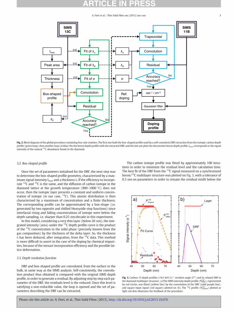
3.2. Box-shaped profile
Once the set of parameters initialised for the DRF, the next step was
to determine the box-shaped profile geometry, characterized by amax-
imum signal intensity Imax and a thickness δ. If the efficiency to incorpo-
rate 12C and 13C is the same, and the diffusion of carbon isotope in the
diamond lattice at the growth temperature (900–1000 °C) does not
occur, then the isotopic layer presents a constant and uniform concen-
tration of isotope (in our case, 13C). This atomic distribution is then
characterised by a maximum of concentration and a finite thickness.
The corresponding profile can be approximated by a box-shape (i.e.
generated by two opposite and shifted Heavyside step functions) since
interfacial rising and falling concentrations of isotope were below the
depth sampling, i.e. sharper than 0.25 nm/decade in this experiment.
In this model, considering a very thin layer (below 20 nm), the inte-
grated intensity (area) under the 13C depth profile curve is the product
of the 13C concentration in the solid phase (precisely known from the
gas composition) by the thickness of the delta layer. So, the thickness
δ has been deduced, after integration, from the 13C data. This method
is more difficult to assert in the case of the doping by chemical impuri-
ties, because of the inexact incorporation efficiency and the possible lat-
tice deformation.
3.3. Depth resolution function
DRF and box-shaped profile are convoluted, from the surface to the
bulk, in same way as the SIMS analysis. Self-consistently, the convolu-
tion product thus obtained is compared with the original SIMS depth
profile, in order to generate a residual. By adjusting step by step each pa-
rameter of the DRF, the residuals level is the reduced. Once this level is
satisfying a non-reducible value, the loop is opened and the set of pa-
rameters describing the DRF can be extracted.
The carbon isotope profile was fitted by approximately 100 itera-
tions in order to minimize the residual level and the calculation time.
The best fit of the DRF from the 13C signal measured on a synchronized
boron/13Cmultilayer structure was plotted on Fig. 3, with a tolerance of
0.3 nm on parameters in order to remain the residual misfit below the
Imax
Thickness Fit of σ
Residual
SIMS
11B
Convolutionλu
λd
σ
Residual
Trapezoidal
Ref.
doping
sec-1 / cm-3
Gaussian filter
Doping
profile
Convolution
z0
Peak area
Box-shaped profile
Fit of λd
Fit of λu
SIMS
13C
Accuracy reached?
Accuracy reached?
Init.
Init.
Init.
Init.
No
Yes
No
Yes
Fig. 2. Block diagramof the global procedure containing four sub-routines. Thefirst one built the box-shapedprofile used by a self-consistent DRF extraction from the isotopic carbon depth
profile (green loop), then another loop (in blue)fits the boron depth profilewith the extractedDRF, and the last one plots thedeconvolve boron depth profile. Imax corresponds to the signal
intensity of the natural 13C abundance found in the diamond.
40 50 60 7040 50 60 70
DRF
Layerb)
Depth (nm)
P13C
Dopant
Residuals
P13C
SIMS
Sig
nal in
tensity (
s-1
)
a)
Depth (nm)
Fit Curve
Fig. 3. Carbon-13 depth profiles (14.5 keV Cs+, incident angle 27°) and its related DRF in
the diamondmultilayer structure. (a)The SIMS intensity depth profile (PSIMS13C ), represented
by red circles, was fitted (yellow line) by the convolution of the DRF (solid purple line),
and square input signal (red square) plotted on (b). The 13C profile (PDopant13C ) plotted as
light red dots illustrates the feedback of the procedure.
3A. Fiori et al. / Thin Solid Films xxx (2013) xxx–xxx
Please cite this article as: A. Fiori, et al., Thin Solid Films (2013), http://dx.doi.org/10.1016/j.tsf.2013.10.076
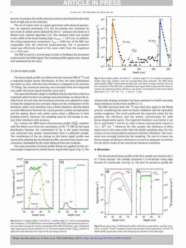
percent. In practice themisfit reduction seems to be limited by the noise
level at high and at low intensity.
The set of values were in a good agreement with physical parame-
ters. As reported previously [15], the ion-mixing was simulated by
ion-recoil of carbon atoms induced by the Cs+ primary ions beam in a
Monte-Carlo method algorithm [16]. The obtained value was similar
to the width of the broad trailing edge (λdown = 3.03 nm). In addition,
the rising exponential component (λup = 0.90 nm) of the DRF was
compatible with the observed backscattering. The σ parameter
value was effectively found of the same order than the roughness
(σ = 0.55 nm).
The DRF is used in a second step, in order to feedback the procedure
to deconvolve the SIMS signal. The resulting profile appears box-shaped
and modulated by the noise.
3.4. Boron depth profile
The boron depth profile was fittedwith the extracted DRF of 13C and
a trapezoid-shaped atomic distribution. At first, the atom distribution
was taken as a box, with the same thickness δ employed in the previous13C fitting. The maximum intensity was calculated from the integrated
area under the boron signal intensity curve and δ.
The input distribution shape is modified step by step from a box to a
trapezoid,which involves anupslope and a downslope, to reduce the re-
sidual level. At each step, the maximum intensity was adjusted in order
to keep the integrated area constant. Slopes are the consequence of the
interfaces width. Such interfaces have a finite thickness, directly linked
to some differences between the crystal growth (carbon incorporation)
and the doping. Boron and carbon atoms show a difference in their
bonding kinetics. However, the sampling must be rich enough to ana-
lyze these interfaces with accuracy.
Fig. 4 shows the SIMS boron concentration profile (PSIMS11B ) together
with the fitted curve from the convolution of the 13C DRF by the input
distribution function. For convenience in Fig. 4, the signal intensity
was converted into atomic concentration from a calibrated sample.
The contribution of the ion mixing on the boron depth profile was
removed by plotting the distribution profile, converted into atomic con-
centration, modulated by the noise deduced from the residuals.
The same procedure of boron profile fitting was applied on the sec-
ond sample composed of a double boron-doped delta layers (Fig. 5). The
related delta-doping technique has been optimized to build extremely
sharp interfaces on the boron profile [5,11].
The DRF extracted from the 13C was used once again in the fitting
process, considering the same ion beam conditions and the equivalent
surface roughness. The result confirmed the expected values for the
position, the thickness, and the atomic concentration for both
boron-doped delta layers. The expected thickness was below 2 nm
for d1 and below 1 nm for d2, with a boron concentration closed to
1.2 × 1021 cm−3. However for this sample, the thickness of delta
layers was in the same order than the depth sampling step. For this
reason, it was not possible to measure interface thickness. The treat-
ment was strongly limited by the sampling. The use of a lower ion
beam energy would have allowed us to reach an adequate resolution
for the direct study of the interfacial chemical transition.
4. Discussion
The deconvolved boron profile of the first sample was found to be 5
to 7 times sharper: the initially measured 1.5 nm/decade rising edge
became 0.3 nm/decade (see Fig. 6). The best fit seemed to justify the
40 50 60 7040 50 60 70
0
1x10²⁰
2x10²⁰
3x10²⁰
4x10²⁰
5x10²⁰
6x10²⁰
7x10²⁰
b)
Depth (nm)
DRF
Distribution
Residuals
P11B
SIMS
11B
co
nce
ntr
atio
n (
at.
cm
-3)
a)
Depth (nm)
Fit Curve
P11B
Dopant
Fig. 4. Boron-11 depth profiles (14.5 keV Cs+, incident angle 27°) and its corresponding
data treatment. (a) The SIMS boron concentration profile (PSIMS11B ) represented by green cir-
cles, was fitted (orange line) by the convolution of the DRF (purple line), and amodulated
input signal (green square) plotted on (b). The boron dopant profile (PDopant11B ) plotted as
light green dots illustrates the result of the ion mixing removal.
150 200 250 300 3501016
1017
1018
1019
1020
1021
Fit of d2
d2
d1
PBoron
SIMS
Fit of d1
Boro
n c
oncentr
ation (
at.cm
-3 )
Depth (nm)
Fig. 5. Boron depth profile (14.5 keV Cs+, incident angle 27°) of a sample containing a
double delta layer together with the corresponding data treatment. The SIMS boron
depth profile (PSIMSBoron) represented by black dots, was fitted (orange and blue lines) by
the convolution of the DRF with a modulated input signal. Both orange and blue boxes il-
lustrate the expected position, thickness, and atomic concentration of the boron-doped
delta layers (1.2 × 1021 cm−3, d1 N 1 nm, d2 N 2 nm).
40 50 60 70
102
103
104
105
40 50 60 70
1018
1019
1020
1021P
11B
Dopant
Sig
nal in
tensity (
s-1
)
Depth (nm)
P13C
SIMS
11B
concentr
ation (
at.cm
-3)
Depth (nm)
P11B
SIMS
b)a)
Layer
Fig. 6. Boron and carbon-13 SIMS depth profiles of the first sample before and after treat-
ment. (a) Initial 11B and 13C plotted in green and red open circles respectively. (b) Final 11B
depth profile (green dots) with a box indicating the position of the delta layer.
4 A. Fiori et al. / Thin Solid Films xxx (2013) xxx–xxx
Please cite this article as: A. Fiori, et al., Thin Solid Films (2013), http://dx.doi.org/10.1016/j.tsf.2013.10.076

presence of a finite thickness for the interface located between boron-
doped and intrinsic diamond layer. Nevertheless, such interface thick-
ness was composed of two points only. The sampling (Δz = 0.9 nm)
was not rich enough to really conclude about an exponential or linear
dependence on the doping transition.
In addition, because of the low sampling rate, it is not possible to
conclude if the point found at the interface on the 13C profile was in or
out of the noise level. This might indicate, for example, an error in the
layer position z0. On one hand, a way to enhance the sampling is to
apply a lower energy ion beam, or to detect less ion types. On the
other hand, the isotopic detection becomesmore difficult at low energy,
because of the decrease in the sputtered matter quantity. In parallel,
other effects like sputter-related distortions and matrix effects are still
present, but they seem to be weak enough to collect adequate informa-
tion on the structure. The fact that a sub-nanometer width could be
measured on a nanometer-rough epilayer suggested that the 3D
features associated to the roughness at the deepest interface of the
delta-doped layer were overgrown in a conformal way by this
layer and by the cap layer, and then sputtered away in a conformal
way during SIMS profiling.
Fig. 7 focuses on the response to a delta layermeasured under differ-
ent primary ions beamenergy in a SIMSCameca IMS 7 f. In this case, pri-
mary ions were O2+ and secondary analysed ions were positive instead
of Cs+ and negative secondary ions. With a 46° incident angle, the
depth sampling (Δz) was 1.8, 0.9 and 0.3 nm for an interaction energy
of 5, 3 and 1 keV respectively. By keeping a constant ratio between
the primary ions energy and the extraction voltage, the incident stayed
constant. Then, energies and incidence angles can be independently
tuned in order to enhance the depth sampling.
The inset in Fig. 7 points out an increase of both the upslope (λup)
and the downslope (λdown) lengths as a function of the primary ion en-
ergy only. This is a direct consequence of ion mixing. When the ion
beam has more energy, the recoil and its induced scatter are expanded
in the volume, increasing the decay lengths at the edges. The analysis
with different ion energies modified the peak concentration and the
peak width, whereas the integrated area remained the same. The λup
and λdown measured on d2 were identical on the layer d1, which con-
firms a conformal growth layer by layer and a conformal sputtering dur-
ing the analysis.
However, other techniques are always necessary for an accurate
calibration of the depth scale. For example transmission electron
microscopy (TEM) can be very useful to check on local variations
and to provide internal standards, such as the position of the layers
and their thicknesses. In particular, High Angle Annular Dark Field
scanning TEM observations of diamond epilayers cross-sections
have been recently shown to be sensitive to the presence of boron
concentrations above 1020 cm−3 [17] and to provide a quantitative
analysis tool with nanometer resolution [18]. We plan to apply such
a technique to the double delta-doped sample shown in Fig. 5.
5. Conclusion
By a local isotope enrichment of diamond, we were able to extract
the instrument response of the SIMS and to characterize the incorpora-
tion of both carbon and boron atoms. These treatments allowed to in-
crease the SIMS resolution, in order to subtract the broadening and
the distortion induced by ion-mixing and to reach the nanometer-
range. This procedure yielded a more reliable characterization by SIMS
of nanometer thin diamond embedded layers containing specific im-
purities over a wide range of concentrations. The conformal growth
layer by layer in the delta-doping was confirmed. For these reasons,
the isotopic diamond delta structure is a powerful calibration tool for
SIMS. Once the SIMS response is known for a specific analysis condi-
tion, the enhanced resolution allows in principle to determine the
position and the thickness of any doped layer, however thin, if the
depth sampling by SIMS is frequent enough.
Acknowledgments
The financial support of Agence Nationale de la Recherche under
contract ANR08-BLAN-0195 and la Région Rhône-Alpes for the bourse
de mobilité Explora'Doc is gratefully acknowledged. This work was
also supported by the Strategic International Collaborative Research
Project from the Japan Science and Technology Agency, Japan and
Grant-in-Aid for Scientific Research from the Japan Society for the Pro-
motion of Science, Japan (No. 23360143).
References
[1] H. Watanabe, S. Shikata, Diam. Relat. Mater. 20 (2011) 980.[2] Y. Shimizu, H. Takamizawa, Y. Kawamura, M. Uematsu, T. Toyama, K. Inoue, E.E.
Haller, K.M. Itoh, Y. Nagai, J. Appl. Phys. 113 (2013) 026101.[3] K. Ohno, F.J. Heremans, L.C. Bassett, B.A. Myers, D.M. Toyli, A.C. Bleszynski Jayich, C.J.
Palmstrøm, D.D. Awschalom, Appl. Phys. Lett. 101 (2012) 082413.[4] R. Edgington, S. Sato, Y. Ishiyama, R. Morris, R.B. Jackman, H. Kawarada, J. Appl. Phys.
111 (2012) 033710.[5] A. Fiori, T.N. Tran Thi, G. Chicot, F. Jomard, F. Omnès, E. Gheeraert, E. Bustarret, Diam.
Relat. Mater. 24 (2012) 175.[6] H. Umezawa, M. Nagase, Y. Kato, S. Shikata, Diam. Relat. Mater. 24 (2012) 201.[7] T. Ishikawa, K.-M.C. Fu, C. Santori, V.M. Acosta, R.G. Beausoleil, H. Watanabe, S.
Shikata, K.M. Itoh, Nano Lett. 12 (2012) 2083.[8] S. Hofmann, Appl. Phys. 13 (1977) 205.[9] Y. Shimizu, A. Takano, K.M. Itoh, Appl. Surf. Sci. 255 (2008) 1345.
[10] M.G. Dowsett, G. Rowlands, P.N. Allen, D. Barlow, Surf. Interface Anal. 21 (1994) 310.[11] G. Chicot, T.N. Thu Nhi, A. Fiori, F. Jomard, E. Gheeraert, E. Bustarret, J. Pernot, Appl.
Phys. Lett. 101 (2012) 162101.[12] M. Kamo, Y. Sato, S. Matsumoto, N. Setaka, J. Cryst. Growth 62 (1983) 642.[13] T. Teraji, T. Taniguchi, S. Koizumi, K.Watanabe, M. Liao, Y. Koide, J. Isoya, Jpn. J. Appl.
Phys. 51 (2012) 090104.[14] B. Gautier, R. Prost, G. Prudon, J.C. Dupuy, Surf. Interface Anal. 24 (1996) 733.[15] A. Fiori, F. Jomard, T. Teraji, S. Koizumi, J. Isoya, E. Gheeraert, Etienne Bustarret, Appl.
Phys. Express 6 (2013) 45801.[16] J.F. Ziegler, M.D. Ziegler, J.P. Biersack, Nucl. Instrum. Meth. Phys. Res. Bull. 268
(2010) 1818.[17] D. Araujo, P. Achatz, R. El Bouayadi, A.J. Garcia, M.P. Alegre, M.P. Villar, F. Jomard, E.
Bustarret, Diam. Relat. Mater. 19 (2010) 972.[18] D. Araujo, M.P. Alegre, J.C. Piñero, A. Fiori, E. Bustarret, F. Jomard, Appl. Phys. Lett.
103 (2013) 042104.
1 50
1
2
3
315 320 325 330 335 340 345
1018
1019
1020
1021
Decay le
ngth
λ (
nm
)
Incident O+
2energy (keV)
λdown
λup
Boro
n c
oncentr
ation (
at.cm
-3)
Depth (nm)
[B]error
λdown
λup
O+
2 5 keV
O+
2 3 keV
O+
2 1 keV
3
Fig. 7. Boron depth profile recordedwithO2+, incident angle 46°, at three different energies
on the layer labelled d2 on the Fig. 6. The inset shows the behaviour of the upslope (λup)
and the downslope (λdown) of the boron profile as a function of the primary ion energy.
5A. Fiori et al. / Thin Solid Films xxx (2013) xxx–xxx
Please cite this article as: A. Fiori, et al., Thin Solid Films (2013), http://dx.doi.org/10.1016/j.tsf.2013.10.076


In situ etching-back processes for a sharper top interface in boron delta-dopeddiamond structures
Alexandre Fiori a,⁎, Thu Nhi Tran Thi a, Gauthier Chicot a, François Jomard b, Franck Omnès a,Etienne Gheeraert a, Etienne Bustarret a
a Institut Néel, CNRS and Université Joseph Fourier, BP166, F-38042 Grenoble, Franceb Groupe d'Etude de la Matière Condensée (GEMaC), UMR 8635 du CNRS, UVSQ, 45 Avenue des États-Unis, 78035 Versailles Cedex, France
a b s t r a c ta r t i c l e i n f o
Available online 14 January 2012
Keywords:Diamond
Delta-doping
Dry etch
SIMS
One of the main challenges of delta-doping of diamond with boron resides in minimizing the width and op-
timizing the structural quality of the interface region between the heavily-doped ultra-thin layer and the non
intentionally doped high mobility epilayers. In this work, we present an in situ etching-back approach to this
problem. In particular, a careful SIMS profiling of the top interface shows that advanced gas switching proce-
dures and adequate in situ O2 and H2 plasma etch steps lead to a rising depth lower than 2 nm per decade
over 3 to 4 orders of magnitude of boron concentration. A specificity of the present work is that the multilayer
structures were obtained without interrupting the microwave plasma during the whole process.
© 2012 Elsevier B.V. All rights reserved.
1. Introduction
Because of the difficulty to obtain n-type doping in diamond andof the depth of the phosphorus donor energy level, most of the efforttoward diamond-based devices has been devoted to unipolar devices.Among these, delta-doped structures have long been consideredpromising for field-effect diamond transistors (FET). Following theinitial proposal to transpose such architecture from GaAs or Si to dia-mond [1], various attempts have been made in the 90s, first in Japan[2], then in Germany [3–5] and Israel [6]. More recently, further de-velopments have emerged in Germany [7–11] and in the UK [11,12].Significant progress has been made in the design and performanceof workable FET demonstration devices. In diamond, such a delta-doped structure would require [13] a metallic boron-doped p++
layer (concentration nB≥5×10²⁰ at.cm−3) less than 3 nm-thick in-tercalated between two non-intentionally doped (NID) layers suitedto high mobility transport [14] (nBb2×1017 at.cm−3).
To our knowledge, no clear evidence has been so far given that themechanisms expected to govern the behavior of a delta-doped FETwere indeed present in any of the devices reported to date: neitherthe confinement of carriers in the delta doped epilayer, nor the delo-calization of holes in a high mobility region. Actually, if one intro-duces into modern simulation tools [13] one of the few boronconcentration profiles published [10] with a dynamical concentrationrange encompassing the four relevant orders of magnitude, it is clear
that a strongly scattered or hopping hole transport along the interfaceregion is expected to contribute significantly and in a detrimentalmanner to the ON transconductance of the FET, and that delocaliza-tion of carriers, if any, occurs only on the steeper top (surface) sideof the delta-doped layer.
In order to detect the confinement effects and enhanced mobilityexpected for an ideal structure, we propose here to test the limita-tions of a classical MPCVD approach for getting sharp interfaces be-tween thin heavily-doped and thicker non-intentionally dopedepilayers. In contrast to most of previously published works, the pro-cesses to be investigated in the following avoid plasma interruptionand/or exposure of interfaces to air.
The boron concentration profiles of typical multilayered stacks ofNID and p++ layers will be discussed. We discarded (111)-orientedgrowth because of the poor quality of the substrate surfaces, and wereduced the growth rate compared to our previous studies [15]. Be-cause slowing down the growth process by reducing the methane tohydrogen ratio is known to decrease significantly the solid state in-corporation efficiency [15] of boron, we had to retort to additionaletch-back strategies which will be discussed in some detail below.
2. Experimental results and discussion
2.1. Experimental details
All diamond films were homoepitaxially grown from a gas phase byMicrowave Plasma-enhanced Chemical Vapor Deposition (MPCVD) ontype Ib 100-oriented 3×3 mm diamond substrates (purchased fromSumitomoElectric). None of the recently developed smoothingprocess-es [16] were applied to the substrate surface, prior to its introduction
Diamond & Related Materials 24 (2012) 175–178
Presented at NDNC 2011, the 5th International Conference on New Diamond and
Nano Carbons, Suzhou, China.
⁎ Corresponding author.
E-mail address: [email protected] (A. Fiori).
0925-9635/$ – see front matter © 2012 Elsevier B.V. All rights reserved.
doi:10.1016/j.diamond.2012.01.018
Contents lists available at SciVerse ScienceDirect
Diamond & Related Materials
j ourna l homepage: www.e lsev ie r .com/ locate /d iamond

into the load–lock chamber of amodified vertical silica tube NIRIM-type
reactor with a base pressure below 10−7 Torr.
The gas introduction system was modified in order to reduce the
lead time to the substrate surface upon switching from one gasmixture
to the next: the total volume of the reaction chamberwasminimized as
much as possible, introduction manifold valves were positioned closer
to the chamber inlet, the total flow rate was increased and a carrier
gas (He ≈60%) was used beside the usual purified H2 (≈40%), CH4,
B2H6 and O2. Similar to MOCVD systems, 3 gas mixtures (NID growth,
etching step and p++ growth) were flowing at their nominal flow
rate and nominal pressure in 3 independent parallel exhaust systems.
According to the process step (in Table 1), the requested process mix-
ture was switched from the exhaust systems to the reaction chamber,
allowing for a virtually instantaneous commutation of gas flows into
the reactor. The totalflow rate in the 2 liter reaction chamberwasmain-
tained at either 2 slm or 0.2 slm by AERA mass flow controllers and the
total pressure at 50 Torr by a self-tuning/digital PID exhaust throttle
valve. Using a carrier gas allows to reduce themethane partial pressure
without affecting the methane to hydrogen molar ratio.
A small amount (0.25%) of O2 was added during growth of the NID
layer at 1% CH4, ensuring high mobility values [17] and a boron con-
tent lower than a few 1017 at.cm−3 even in the presence of undesir-
able boron-related radicals introduced during previous p++ growth
steps. NID growth was performed at 910 °C, as measured by a single
color infrared pyrometer.
In between NID and p++ growth steps, the carrier gas of helium and
hydrogen was kept flowing and the plasma power modulated to reach
the temperature of the next growth (or etching) step. The duration of
this transition step was 3, 10 or 30 min as specified in Table 1.
The epitaxial growth of the p++ epilayer was performed at a tem-
perature of 830 °C for various molar ratios in the gas phase: the meth-
ane concentration CH4/(H2+He) was reduced to 0.5 and 0.25%
(instead of 4% previously [15]), while the boron to carbon ratio was in-
creased to 6000 and even 8000 ppm, instead of typically 1500 ppm in
previous works [15].
The in situ etching back was performed at 910 °C in a methane-
free and diborane-free atmosphere consisting of 0.25% O2 in the H2
and He carrier gas mixture.
SIMS measurements were performed in a Cameca IMS 4f appara-
tus using two different settings: first, 10 keV Cs+ primary ions inci-
dent at 27° on the surface, and a 4.5 keV extraction potential of
secondary negative ions (14.5 keV impact energy); second, O2+ pri-
mary ions at 47° incidence angle (impact energy 5.5 keV) and a detec-
tion of positive secondary ions. Although the second configuration
was expected to induce less ion mixing and hence lead to a better
depth resolution, it yielded very similar “rising length” values, indi-
cating that this measurement was not limited by the depth resolution
of the instrument. Additional care was taken to ensure both a high
stability of the primary current and a slow enough scanning rate
yielding very flat analysis horizontal sections.
In some cases a lower number of masses were detected in order to
enhance the sampling rate. A diamond reference implanted with
2×10¹⁵ B.cm−2wasmeasured in the same run for calibration purposes.
The depth scale was deduced from the final sputtered crater depth.
2.2. Slow growth and heavy doping
Themost obviousway of reducing the growth ratewithout lowering
too much the boron concentration was to reduce the partial methane
pressure in the gas phase from the 4% value used for superconducting
epilayers [15] down to 0.25%. This led to a growth rate reduced by
about one order of magnitude, in principle also favorable to the control
of small thicknesses. In order to compensate for the lower incorporation
efficiency usually observed at lower CH4 partial pressures [15], the B/C
ratio in the gas phase was increased to 8000 ppm. A multilayer stack
consisting of seven NID layers separating six such p++ layers was
grown. In this sample, two process parameters were varied from layer
to layer : the transition step in the H2 and He carrier gas mixture after
p++ growth,which lasted 30, 10 or 3 min, and the p++ nominal growth
timewhichwas 5 min for the first p++ epilayers (#1 to #3) and 10 min
for the last ones (#4 to #6). The resulting boron SIMS profiles shown in
Fig. 1 did not feature any plateau and the boron peak absolute concen-
tration remained slightly below 4×10²⁰ at.cm−3, i.e. below the
insulator-to-metallic transition threshold for such (100)-oriented epi-
layers [15]. Also, in the case of the 5 min growth, the boron peak con-
centration was not constant from layer to layer, whereas in the case of
the 10 min growth it was the minimum boron concentration in the
NID spacer layer that increased slightly from layer to layer. On the sur-
face side of the p++ layers, the width of the transition in the SIMS pro-
file was characterized by a “rising length” of the boron concentration
varying between 15 and 5 nmper decade depending on the process pa-
rameters. On the substrate side of the same, thewidth of the interface as
Table 1
Time table of growth sequences. The sequence #A is used on samples shown in Figs. 1 and 2. The sequence #B is used on the sample shown on Fig. 3. Each step of the sequence is
displayed on column 1…20 in which is specified the duration of the plasma recipe (in minutes) tagged on corresponding line.
Time table (in minutes)
Sequence #A H2 + He 3 10 30 3 10 30
p++ 5 5 5 10 10 10
NID 50 20 20 20 20 20 10
Sequence #B H2 + He+O2 3 6 10 15
H2 + He 3 3 3 3 3
p++ 4 4 4 4 4
NID 33 15 15 15 15 10
Step number 1 2 3 4 5 6 7 8 9 10 11 12 13 14 15 16 17 18 19 20
Fig. 1. Boron concentration profiles determined by SIMS on amultilayer composed of NID
layers separating six p++ layers following the sequence#A (see Table 1) grownat ameth-
ane molar ratio of 0.25% with B/C=8000 ppm in the gas phase. The first three p++ layers
to be grown (closer to the substrate, i.e. on the right-hand side)were grown for 5min, the
last three p++ layers for 10 min. In both cases the H2 and He transition plasma after p++
growth was maintained during 3 min, 10 min and finally 30 min respectively from right
(substrate bottom interface) to left (top free surface).
176 A. Fiori et al. / Diamond & Related Materials 24 (2012) 175–178

detected by SIMS was about constant, with a typical “decay length” of
the boron concentration around 8 nm per decade.
A boron concentration plateauwas clearly observedwhen themeth-
ane molar ratio was increased to 0.5%, as shown in Fig. 2a for another
sample grown according to the same process sequence. A second obser-
vation was that the NID spacer layers grown in presence of oxygen
maintained in all cases a boron concentration around 1017 at.cm−3,
with a “tail” on the left-hand (top) side which is shown in Fig. 2b to de-
pend on the duration of both the p++ growth (as expected) and of the
H2 and He plasma transition step: for longer transitions and longer p++
growths, the topside interface was steeper above 1018 at.cm−3 (rising
length reduced from 12 nm per decade for layer #1 of Fig. 2a to 6 nm
per decade for layer #6), but the tail detected below this value became
somewhat broader. The effect of the duration of the transition step was
attributed to a slow etch (≤0.3 nm.min−1) of the p++ layer by the H2
and He plasma.
All boron concentration peaks shown in Figs. 1 and 2 had a similar
“decay length” on the right-hand (substrate) side, typically 7–8 nm
per decade. To first order, this length was independent of the meth-
ane molar fraction or of the total flow rate (above 0.2 slm), in contrast
to the delay time for changing the concentration by 2 orders of mag-
nitude which was estimated by mass spectrometry (plasma off) to be
below 10 s in a laminar flow of 2 slm. This suggests that an additional
delay occurs at the surface or related to plasma chemistry, which may
be specific to boron. Further studies are clearly needed on this matter.
2.3. In situ etch process
An intermediate etching step particularly efficient at 910 °C was
provided by adding O2 to the H2 and He mixture with a molar fraction
of 0.25%, the same as during NID growth, but significantly lower than
the 2% value used by other authors for in situ pre-growth etching of di-
amond substrates [18]. The resulting profiles are shown in Fig. 3 where
five p++ epilayers grown at CH4/H2 and B/C molar ratios in the gas
phase of respectively 0.5% and 6000 ppm were etched up to 15 min in
the O2 in H2 and He plasma. The thicknesses of the p++ layers vary lin-
early with the time of exposure to this plasma, yielding an etching rate
of 4.7 nm.min−1. Also, the non-intentional doping level in the spacer
layer was found to be slightly lower for longer exposures, illustrating
the efficiency of this diluted oxygen plasma to reduce “memory effects”
in our reactor. A closer look at these profiles is provided by Fig. 2bwhere
they are superimposed in such a way as to illustrate the effect of the in
situ etch-back process under discussion. Various SIMS measurements
under widely varying profiling conditions have convinced us that lon-
ger etch-back yielded sharper topside interface. The half-width values
obtained after 10 min or more are below 2 nm per decade, close to
the expected depth resolution of the SIMS equipment, or to the lowest
value reported in the literature [12]. The surface roughness remains
lightly deteriorated (Sa≪1 nm) when the etching time is short. If the
etching time is longer than 15 min, then the surface roughness
becomes significantly worse. This was quite encouraging for an
unoptimized process where the plasma was not interrupted.
3. Summary
Ourmodifications of vertical silica tube NIRIM-type reactor and spe-
cial process gas management allows slow growth, heavy boron doping
and in-situ etching of diamond. Multilayers and single delta-layers
have been grown without hydrogen and helium plasma interruptions.
The addition of oxygen is necessary during the NID growth to keep a
low boron concentration. Also, the presence of O2 in H2 and He
Fig. 3. Original (a) and Superimposed (b) SIMS profiles of the boron concentration in a di-
amondmultilayer grown byMPCVDwhere each p++ layer has been etched in-situ for dif-
ferent times in an H2 + He+O2 plasma following the sequence #B (see Table 1). The
resulting rising lengths are given in nm per decade of boron concentration.
Fig. 2. Original (a) and superimposed (b) boron concentration profiles determined by
SIMS on a multilayer composed of NID layers separating six p++ layers following the se-
quence #A (see Table 1) grown at a methane molar ratio of 0.5% with B/C=6000 ppm
in the gas phase. For the two series of layers grown during 5 min and 10 min, the duration
of the H2 and He plasma after p++ growth took three values: 3 min, 10 min and finally
30 min from right (substrate bottom interface) to left (top free surface).
177A. Fiori et al. / Diamond & Related Materials 24 (2012) 175–178

methane-free and diborane-free plasmas provided an efficient in-situ
etching of p++ epilayers, leading to a lower boron contamination i.e.
less “memory effect” in the NID epilayer and to a significantly sharper
top side interface (SIMS rising length below 2 nm per decade). Howev-
er, the boron concentration decay length at the substrate side interface
was still too large to ensure the efficient carrier delocalization effects
expected from such diamond delta-doped multi-layered structures [1].
Acknowledgments
The financial support of Agence Nationale de la Recherche under
contract ANR08-BLAN-0195 is gratefully acknowledged. Gauthier
Chicot held a doctoral fellowship from la Région Rhône-Alpes.
References
[1] T. Kobayashi, T. Ariki, M. Iwabuchi, T. Maki, S. Shikama, S. Suzuki, J. Appl. Phys. 76(1994) 1977.
[2] H. Shiomi, Y. Nishibayashi, N. Toda, S. Shikata, IEEE Electron Device Lett. 16(1995) 36.
[3] A. Vescan, P. Gluche, W. Ebert, E. Kohn, IEEE Electron Device Lett. 18 (1997) 222.[4] M. Kunze, A. Vescan, G. Dollinger, A. Bergmaier, E. Kohn, Carbon 37 (1999) 787.
[5] A. Aleksov, A. Vescan, M. Kunze, P. Gluche, W. Ebert, E. Kohn, A. Bergmaier,G. Dollinger, Diamond Relat. Mater. 8 (1999) 941.
[6] C. Uzan-Saguy, R. Kalish, R. Walker, D.N. Jamieson, S. Prawer, Diamond Relat.Mater. 7 (1998) 1429.
[7] A. Aleksov, M. Kubovic, N. Kaeb, U. Spitzberg, A. Bergmaier, G. Dollinger, Th.Bauer, M. Schreck, B. Stritzker, E. Kohn, Diamond Relat. Mater. 12 (2003) 395.
[8] A. Aleksov, A. Denisenko, M. Kunze, A. Vescan, A. Bergmaier, G. Dollinger, W.Ebert, E. Kohn, Semicond. Sci. Technol. 18 (2003) S59.
[9] A. Denisenko, E. Kohn, Diamond Relat. Mater. 14 (2005) 491.[10] H. El-Hajj, A. Denisenko, A. Bergmaier, G. Dollinger, M. Kubovic, E. Kohn, Diamond
Relat. Mater. 17 (2008) 409.[11] H. El-Hajj, A. Denisenko, A. Kaiser, R.S. Balmer, E. Kohn, Diamond Relat. Mater. 17
(2008) 1259.[12] R.S. Balmer, I. Friel, S.M. Woolard, C.H.J. Wort, G.A. Scarsbrook, S.E. Coe, H. El-Hajj,
A. Kaiser, A. Denisenko, E. Kohn, J. Isberg, Philos. Trans. R. Soc. A 366 (2008) 251.[13] A. Fiori, J. Pernot, E. Gheeraert, E. Bustarret, Phys. Status Solidi A 207 (2010) 2084.[14] J. Pernot, P.N. Volpe, F. Omnès, P. Muret, V. Mortet, K. Haenen, T. Teraji, Phys. Rev.
B 81 (2010) 205203.[15] E. Bustarret, Phys. Status Solidi A 205 (2008) 997.[16] T.N. Tran Thi, B. Fernandez, D. Eon, E. Gheeraert, J. Härtwig, T. Lafford, A.
Perrat-Mabilon, C. Peaucelle, P. Olivero and E. Bustarret, phys. stat. sol. (a)208 (9) (2011) 2057–2061.
[17] P.N. Volpe, J. Pernot, P. Muret, F. Omnès, Appl. Phys. Lett. 94 (2009) 092102.[18] A. Tallaire, J. Achard, F. Silva, R.S. Sussmann, A. Gicquel, E. Rzepka, Phys. Status
Solidi A 201 (2004) 2419.
178 A. Fiori et al. / Diamond & Related Materials 24 (2012) 175–178

Boron incorporation issues in diamond when TMB is used as precursor: Towardextreme doping levels
Pierre-Nicolas Volpe a,⁎, Jean-Charles Arnault a, Nicolas Tranchant a, Gauthier Chicot b, Julien Pernot b,François Jomard c, Philippe Bergonzo a
a CEA LIST, Diamond Sensors Laboratory, F-91191 Gif-sur-Yvette, Franceb Institut Néel-CNRS & Université Joseph Fourier, 25 avenue des Martyrs, BP 166, 38042 Grenoble, Francec GEMaC, Campus du CNRS de Meudon, 1 place Aristide Briand, 92195 Meudon, France
a b s t r a c ta r t i c l e i n f o
Article history:
Received 26 August 2011
Received in revised form 14 December 2011
Accepted 20 December 2011
Available online 27 December 2011
Keywords:
Diamond
Growth
Doping
TMB
Oxygen
Boron doped diamond (BDD) is a very promising material for high frequency and high power applications
like Field Emission Transistors and Schottky diodes. Such electrical devices are usually composed of stacked
highly BDD layers ([B]>5×10²⁰ at·cm−3) on doped at low levels ones ([B]b1017 at·cm−3). In particular,
when delta doping structures are sought, their development implies the accurate control of the highly BDD
layer thickness at the nanometric scale, and, the achievement of high crystalline quality for low BDD layers
with, well defined doping gradients and low roughness at the interfaces. Since several decades, various gas-
eous precursors, most frequently diborane (B2H6) and TriMethylBoron—TMB (B(CH3)3), have been used to
grow BDD layers. TMB is generally seen as a good alternative to diborane as it is less toxic and easier to handle
while it offers expected similar doping properties. In this study, we determine several strategies to grow,
using in a metallic wall MPCVD reactor with TriMethylBoron (TMB, B(CH3)3) as dopant, high crystalline qual-
ity very poorly and highly doped (100) diamond layers. We investigated a wide boron incorporation ([B])
typically between 1016 at·cm−3 up to 5×10²¹ at·cm−3. We will especially insist on two growth strategies
to produce monocrystalline diamond doped at low levels, consisting either to use very low (B/C)gas ratio dur-
ing growth, or to feed oxygen during growth at a constant (B/C)gas ratio. Comparison of these two strategies
will be assessed from low temperature Cathodoluminescence (CL), Secondary Ion Mass Spectroscopy (SIMS),
C(V) and Hall effect measurements on several layers. The effects of oxygen on boron atoms, when TMB is
used as doping gas will also be studied in detail and commented. In a second part, we will especially inves-
tigate the synthesis of highly BDD diamond layers ([B]>5×10²⁰ at·cm−3). SIMS analysis enables to identify
the existing links between growth conditions ([CH4]/[H2] and (B/C)gas ratios, pressure, temperature) and the
boron incorporation into the diamond matrix. We will finally show that, under optimized growth regimes,
the metallic-semiconductor transition above 1021 at·cm−3 of boron can be routinely achieved.
© 2011 Elsevier B.V. All rights reserved.
1. Introduction
According to its intrinsic properties, like wide band gap (5.45 eV),
high hole saturation velocity (2.7×107 cm·s−1) [1], very low permit-
tivity (5.87) and high hole Hall mobility (2000 cm2/Vs) at room tem-
perature [2,3], p-type diamond is a promising material for high power
[4–6] and high frequency electronic applications [1,7–9]. The achieve-
ment of such devices generally requires the growth of stacked struc-
tures with highly ([B]>5×10²⁰ at·cm−3) and poorly doped diamond
films ([B]b5×1015 at·cm−3), exhibiting high crystalline quality and
high mobilities at room temperature (μ@RT). The synthesis of low
BDD layers with such properties represents a great challenge due to
the relatively uncontrolled residual boron levels in CVD growth reac-
tor and the poor mastering of the acceptor passivation and compen-
sation phenomenon. Achard et al. [10] showed that high crystalline
quality diamond layers could be achieved in an MPCVD reactor only
using CH4 and H2. However, those layers exhibited a small boron con-
tamination (1015 at·cm−3b [B]b1016 at·cm−3) mainly due to the re-
actor residual contamination [9]. On the other hand, with the same
growth technique, very low doped diamond layers have been already
obtained but with a fluctuating acceptor concentration over more
than one decade (2×1014 cm−3b [Na]b3×1015 cm−3) [6]. The latter
results have been more recently confirmed by others [5] showing
that, using exclusively a CH4/H2 gas mixture, fluctuation of the accep-
tor concentration over several decades can appear over 50% of the
total layer thickness. Very recently, Volpe et al. [9] achieved very
low boron doped diamond layers ( [B]~1016 at·cm−3) in a NIRIM
type reactor by using diborane as dopant gas, and, showed that
Diamond & Related Materials 22 (2012) 136–141
⁎ Corresponding author. Tel.: +33 1 69 08 29 76.
E-mail address: [email protected] (P.-N. Volpe).
0925-9635/$ – see front matter © 2011 Elsevier B.V. All rights reserved.
doi:10.1016/j.diamond.2011.12.019
Contents lists available at SciVerse ScienceDirect
Diamond & Related Materials
j ourna l homepage: www.e lsev ie r .com/ locate /d iamond
small amounts of oxygen ([O2]/[H2]=0.25%) injected during growth
[11,12] permit to reach [10] and control [1] very low doping levels,
as well as to achieve mobilities at room temperature at the state of
art [3]. These results confirmed those from Harris et al. [13] which evi-
denced that adding oxygen leads to an increase of H atommole fraction
(known to be one of the growth key parameter [14]), a removal of non
carbon species, and more globally an increase of the layer crystalline
quality. Moreover, Ruan et al. [14] demonstrated that the injection of
oxygen into the gas phase during p-type polycrystalline diamond
growth can decrease the boron incorporation as well as improve dia-
mond crystals quality. Meanwhile, all the studies mentioned above
have been carried out using B2H6 as doping gas.
More recently, Remes et al. [15] reported on the achievement of
(111) BDD layers with TMB and oxygen. They mentioned that adding
O2 does not modify the boron doping level but increases drastically
the compensation of the latter due to the formation of B–O complex
into the matrix. However, this study has been performed on (111)
p-type layers which are known to be more defective than (100) p-
type layers. The exact role of oxygen for low BDD layers synthesis
seems to depend principally on the gaseous precursors used, and
need then to be checked more precisely for (100) oriented CVD
layers.
In this study, we synthesized (100) poorly BDD layers in a metallic
wall reactor with TMB as doping gas to investigate the effect of oxy-
gen on the boron concentration [B], the acceptor concentration [Na]
and the crystalline quality of the layers with respect to the [O2]/[H2]
ratio. The doping efficiency of TMB will be compared to that of dibor-
ane. In a second part, we present a growth strategy allowing the
achievement of highly BDD layers ([B]>5×10²⁰at·cm−3) in a metallic
wall reactor using TMB. Several groups [16,17] reported a saturation
of boron concentration levels below the metallic-semiconductor
transition. We will show that, if, doping limitation appears around
1020 at·cm−3, the latter, can be overcome by drastically modifying
the growth conditions. Finally, we demonstrate that the boron concen-
tration is more precisely linked to the power density of the microwave
plasma. Using optimal conditions, highly BDD layers can be reproduc-
tively grown with a low growth rate (0.25 μm/h) and a boron concen-
tration higher than 1021 at·cm−3.
2. Experimental
BDD layers were grown using Microwave Plasma Chemical Vapor
Deposition (MPCVD) on Ib (100) HPHT (3×3×0.5 mm3) diamond
substrates from Sumitomo company. We used two home-made
water cooled metallic wall chamber CVD reactors, each devoted to
low and high boron concentrations, respectively. Growths were initi-
ated using an in-situ H2 plasma of 30 min at a pressure of 100 mbar
and a temperature of 870 °C. Growth parameters are detailed in
Table 1 for low and highly BDD layers respectively. Secondary-ion
mass spectrometry (SIMS) was performed using a Cameca IMS 4F
equipment to obtain the depth distribution of boron atoms into the
diamond matrix. Low BDD layers have been characterized using CL
measurements performed at 5 K, with an accelerating voltage from
5 kV to 10 kV, in a QUANTA 200 SEM microscope through an HR
460 JOBIN YVON spectrometer. For acceleration voltages of 5 kV and
10 kV, the depth probed by the electron beam is of 0.5 μm and 1 μm,
respectively [18,19]. CL energy resolution of the set-up is around
2 meV according to our experimental conditions. The considered cri-
teria to appreciate the layers crystalline quality is the Full Width at
Half Maximum (FWHM) of the relative intensities, and, the integrated
areas of the FETO and A band signals located at 5.26 and 3 eV
respectively.
Some of the low BDD layers synthesized using different [O2]/[H2]
ratios have been also processed with MESA Hall bars using Ti
(30 nm)\Pt (50 nm)\Au (40 nm) ohmic contacts annealed at 750 °C
under vacuum. Hall effect measurements were carried out with a
high input impedance system and a DC magnetic field B with an am-
plitude of 0.8 T in a configuration where B is parallel and j, the current
density, is perpendicular to the growth axis (100) respectively. Ring
shape Schottky diodes made of aluminum (Ø=200 μm diameter
and 100 nm thick) and Ti (30 nm)\Pt (50 nm)\Au (40 nm) as
Schottky and ohmic contacts, respectively, have been also used on
the latter samples surface after a surface oxidation performed by
ozone treatment [20]. The results of the Hall and C(V) measurements
are used for the discussion.
3. Results and discussion
3.1. Growth of diamond layers doped at a low level ([B]b1017 at·cm−3)
Two growth strategies were compared using TMB as doping gas in
our two metallic wall reactors. The first technique (CG1) uses a [CH4]/
[H2] gas mixture [5] while the second (GC2) consists of adding a small
percentage of oxygen during growth with a small amount of doping
gas as previously reported for diborane [3]. To check the evolution
of the [B] versus the amount of oxygen, we used here a (B/C)gasratio of 5020 ppm giving [B]=2×10¹⁹ at·cm−3 when [O2]/[H2]
=0%. Growth parameters used for both techniques are summarized
in Table 1.
3.1.1. Poorly BDD layers grown using CH4/H2 mixture (GC1)
Fig. 1 shows the CL spectra obtained on a 15 μm thick layer grown
using GC1. The excitonic peaks (5.21 eV–5.26 eV) intensity is signifi-
cantly higher than the one from defects band induced by to extended
defects, (by a factor ~25) located at 3 eV and 3.7 eV (Fig. 1(b)). More-
over, the three orders of the excitonic peaks can be clearly identified
at 5.26 eV, 2.62 eV and 1.74 eV (Fig. 1(b)). The FWHM of the FETO
peak has been evaluated at 7.8 meV, which confirms the high crystal-
line quality of the diamond layer.
Fig. 2 shows the SEM image of the hydrogenated diamond surface.
The film roughness seems to be very low and no non-epitaxial crys-
tallites can be seen on the image. Some hillocks can be observed exhi-
biting the presence of threading dislocations with linear geometry
related to the propagation of induced polishing defects of the Ib sub-
strate through the CVD layer [21,22]. From Fig. 1, a boron contamina-
tion within the layer can also be identified by the BETO located at
5.21 eV associated to boron bound exciton recombinations. The num-
ber of acceptors has been quantified [21,22] to [Na]=(5.6±
1.8)×1016 cm−3. As no boron dopant has been intentionally injected
during growth, this acceptor concentration is a signature of the boron
Table 1
Growth conditions used for BDD layers.
Growth conditions [CH4]/[H2]
(%)
(B/C)gas(ppm)
[O2]/[H2]
(%)
P
(mbar)
T
(°C)
Microwave power
(W)
Growth rates
(μm/h)
GC1 0.2 0 0 120 870 474 0.28
GC2 0.2 5020 0 to 1 120 870 570 0.22–0.15
GC3 0.2–4 3000–40,000 0 70 870 495 0.2–1.4
GC4 0.55 21,482 0 20–120 750–870 438 0.1–0.25
137P.-N. Volpe et al. / Diamond & Related Materials 22 (2012) 136–141
residual level of our CVD reactor. Thus, growing diamond layers
using only a CH4/H2 gas mixture is a good way to produce high crys-
talline quality films, nevertheless, this strategy prevents the good
mastering of low boron doping levels [5]. Indeed, the residual
boron is strongly dependent on the history of the reactor. Moreover,
the peak located at 3.18 eV is characteristic of substitutional nitrogen
into the CVD layer [23] (Fig. 1(b)). This first growth strategy is also
limited to provide low contaminated layers. These results are con-
firmed by other studies [5]. Some authors also underlined that layers
grown using CH4/H2 contain large amount of hydrogen atoms leading to
a strong passivation of the boron atoms [5]. In summary, CG1 enables
to achieve remarkably good crystalline quality even if, the boron
content does oscillate around the residual level, and, a weak boron
compensation may appear due to the presence of substitutional nitrogen
atoms.
3.1.2. Growth of diamond layers doped at a low level by using CH4, H2, O2
and TMB (GC2)
Growth conditions are mentioned in Table 1. A pressure of
120 mbar and a (B/C)gas ratio of 5020 ppm have been used for all
the layers. The evolution of the boron concentration [B] as measured
by SIMS, and, the BETO/FETO ratio as determined using CL have been
plotted versus the [O2]/[H2] ratio in Fig. 3.
The boron concentration [B] measured by SIMS decreases with the
[O2]/[H2] ratio by three orders of magnitude (see Fig. 3(a)) for
0≤ [O2]/[H2]≤1%. For [O2]/[H2]=0.25%, a [B] decrease of two de-
cades (by comparison with [O2]/[H2]=0%) can be observed which
is consistent with previous reports [3,11,14] when diborane is used
as doping gas. Moreover, we can also observe that the addition of
oxygen permits to reach incorporations below the residual boron
level. At a given [O2]/[H2] ratio (b0.8%), the boron concentration fluc-
tuations are very close to the BETO/FETO ratio fluctuations, hence to
values of [Na] measured by CL indicating a very weak compensation.
This clearly shows that no significant compensation is induced by ox-
ygen even if TMB is used as doping gas. This statement infirms the
previous hypothesis [15] of a possible creation of B–O pairs when
TMB and oxygen are used to grow CVD diamond layers. The low con-
ductivity observed by these authors seems to be more associated to
the (111) orientation of the CVD layers which is known to be a
more unfavorable orientation for the achievement of uncompensated
BDD layers [26]. As opposed to CG1, the CG2 growth strategy using
oxygen, enables to reach [B] concentrations that are lower than the
residual boron levels within the reactor (Fig. 2), with values as low
as 2×1016 cm−3. The evolution of the FETO FWHM, and, the A band
integrated area versus the [O2]/[H2] ratio are plotted in Fig. 2(b). A
minimum for A band area is reached for a ratio [O2]/[H2]~0.2%. This
[O2]/[H2] ratio also leads to an increase of the layer crystalline quality
according to FETO FWHM profile. This result is in agreement with the
one obtained for [O2]/[H2]=0.25% for CVD growth performed with
B2H6 [11]. Thus, to optimize the CVD layer quality, oxygen has to be
injected into the chamber with a ratio [O2]/[H2] close to 0.25%, inde-
pendently of the gaseous precursor used.
The CL spectra of a layer grown using [O2]/[H2]=0.25% is shown in
Fig. 3. The intensity of the A band located at 3 eV is almost twice higher
than the FETO intensity (Fig. 3(b)). Meanwhile, the three orders of the
FETO and BETO, located at 5.26 eV and 5.21 eV (first order), 2.63 eV
and 2.605 eV (second order), and 1.75 eV and 1.73 eV (third order)
are present indicating a good crystalline quality. Moreover, the low
FWHM (9.7 meV) of the FETO suggests a low localized defects density
(Fig. 3(a)). Meanwhile, a H3 signal related to N–V–N or V–N–N–V de-
fects [25], can be detected at 2.45 eV (Fig. 4(b)) which drives us to the
conclusion that, for an accelerating voltage of 5 keV, a clear signature
of the Ib substrate also appears on the spectra [27].
Davies et al. [18] showed that for an accelerating voltage of 5 kV, the
depth probed by the primary electrons is around 265 nmwhich is lower
than the layer thickness (400 nm) evaluated by SIMS. Previous studies
on the determination of excitonic diffusion length (λ) showed, for in-
trinsic CVD layers, that λ can be higher than several microns [2,27–
29]. In our layers [Na] has been evaluated at (1.4±0.4)×1017 cm−3
which implies that λ should be a lot smaller than the one found into in-
trinsic diamond layers [2,27–29]. If we assume a primary electron ener-
gy of 5 keV, we can deduce that λ should be at least of 125 nmwhich is
approximately twice lower than the electrons' penetration depth. In
such experimental conditions, we clearly observe that excitonic recom-
bination can also occur in the Ib substrate [27] which may induce that
the signal at 3.2 eV from substitutional nitrogen comes from the sub-
strate. This hypothesis is confirmed by previous studies [11,23], which
Fig. 1. Cathodoluminescence spectra, performed at 5 K and 10 keV, of a layer grown using the GC1 approach (see text): (a) on the excitonic peaks range, (b) on the whole energy range.
Fig. 2. SEM image of the hydrogenated diamond surface (INLENS mode, accelerating
voltage of 2 kV).
138 P.-N. Volpe et al. / Diamond & Related Materials 22 (2012) 136–141

showed that the use of oxygen limits the incorporation of host atoms
like nitrogen or silicon [3,12] into the diamond matrix. As a matter of
fact, we can also suppose that the strong A band signal is partially com-
ing from the substrate which further complicates the interpretations
based on the ratio of FETO and A band intensities.
Hall effect measurements and C(V) analysis were performed on
three samples synthetized with [O2]/[H2] contents of 0.125% (sample
#1), 0.25% (sample #2) and 0.375% (sample #3). A decrease of the
Hall carrier density and an increase of the resistivity can be respec-
tively observed with respect to the [O2]/[H2] ratio increase as shown
in Fig. 5. This behavior is consistent with the previous observations
made on the ratio BETO/FETO and [B] (Fig. 3) and is in agreement
with studies made with diborane [3,11]. The non-compensated ac-
ceptor concentrations [Na–Nd] mentioned in Table 2 have been eval-
uated by C(V) measurement at a depth where the doping profile is
constant (200 nm form the surface). Deeper, the [Na–Nd] decreases
down to some 1016 cm−3 at the layer/substrate interface for samples
#2 and #3. The nitrogen donors of the Ib substrate, more precisely the
depleted area associated to the pn junction, is certainly at the origin
of the electrical inactivation of the acceptor levels near the sub-
strate/epilayer interface. This not flat [Na–Nd] profile leads to a poor ac-
curacy on the values determined from the Hall carrier density fitting by
neutrality equation. As expected, the [Na] evaluated by Hall effect and
reported in Table 2 are lower than the [B] measured by SIMS. Moreover,
the room temperature Hall carrier mobilities of the three samples are
elevated (900 and 1200 cm2/Vs) thus confirms the low compensation.
The mobility values achieved using TMB are near the state of the art of
the maximum hole mobility achievable in diamond [3], and confirm
the interest of this precursor for electronic devices fabrication. We
showed that adding oxygen when TMB is used as doping gas enables
to decrease the boron concentration of (100) diamond layers below
the boron residual contamination of the reactor. Using combined SIMS
and CL measurements, we demonstrated that oxygen does not induce
any compensation of the acceptors from the creation of B–O pairs as
previously proposed [16]. An optimal [O2]/[H2] ratio was determined
close to 0.25% leading to an increase of the layer crystalline quality,
and a decrease of [B] and [Na] of two decades. Finally, Hall mobility at
room temperature led to values close to the state of art for layers
grown between 0.125%b [O2]/[H2]b0.375%. We can conclude that Hall
mobility, [B] and crystalline quality evolutionswith oxygen content, ob-
served with TMB are very similar to those previously observed with
Fig. 3. (a) Evolution of the boron concentration [B] (empty circles) and the BETO/FETO ratio (full circles) measured by SIMS and CL at 5 K and 10 keV respectively, with respect to the
[O2]/[H2] ratio. The incertitude on the SIMS measurements has been evaluated at 10% of the boron content. The horizontal broken line represents the residual boron level of the
reactor. (b) Evolution of the FETO (empty squares) intensity and FWHM (full squares) measured by CL at 5 K and 10 keV with respect to the [O2]/[H2] ratio.
Fig. 4. Cathodoluminescence spectra, performed at 5 K and 5 keV, of a CVD layer grown with growth strategy 2 (CG2) ([O2]/[H2]=0.25%, (B/C)gas=5020 ppm):(a) on the excitonic
peaks range, (b) on the whole energy range.
Fig. 5. (a) Hall density and (b) resistivity evolutionswith respect to (1/T) andT respectively
for samples #1 (open circles), #2 (open squares) and #3 (open triangles). The continuous
lines in Fig. 4 (a) represent the fittings of the experimental data [25].
139P.-N. Volpe et al. / Diamond & Related Materials 22 (2012) 136–141

B2H6 [3,11,12,24]. The best results were obtained with a [O2]/[H2] ratio
of 0.25%.
3.2. Growth of highly BDD layers ([B]>1020 at·cm−3)
The MPCVD growth of high BBD layer in a metallic wall reactor
was carried out using TMB as dopant gas. The corresponding growth
parameters are listed in Table 2. Several sets of highly BBD layers
were prepared by tuning the growth conditions via [CH4]/[H2] and
(B/C)gas ratios Table 2. Boron incorporations [B] as measured by
SIMS are reported in Fig. 6 versus (B/C)gas ratio.
Moreover, at a constant (B/C)gas ratio, the boron concentration in-
creases with the [CH4]/[H2] ratio. Similar trends were obtained on
(100) and (111) BDD films grown in a NIRIM type reactor using
diborane [30] where it was demonstrated that boron concentration
is cross linked with the methane concentration in the gas phase. In
addition, [B] increases linearly with the (B/C)gas ratio for
0.15%≤ [CH4]/[H2]≤6%. The same behavior can be observed in Fig. 6
for [CH4]/[H2]≤0.55% ratio. However, for higher methane contents, a
saturation appears close to 3×10²⁰ at·cm−3. This saturation was also
reported by two other groups [16,17] who synthetized (100) high BDD
layers using diborane in ametallic wall reactor. The origin of this satura-
tion is not clear up to now. On the other hand, one has to tka into
account that if diborane is used in a NIRIM reactor, the semiconductor–
metal transition was overcome using a (B/C)gas>1000 ppm and [CH4]/
[H2]>4% [30]. If a saturation appears independently of the doping gas
nature, this could be related to the growth conditions (gas mixture,
pressure, temperature), or, to the reactor type (metallic wall or
NIRIM). To check the first hypothesis, diamond layers were synthesized
using CG4 conditions for gas pressures ranging from 20 to 120 mbar.
Boron concentrations measured by SIMS are plotted versus pressure
in Fig. 7.
The power density of the microwave plasma has been estimated
by dividing the microwave power by the approximated volume of
the plasma ball assuming a spherical shape. Its evolution with
respect to the gas pressure is displayed in Fig. 6. The microwave
power was maintained constant during the experiments. Thus, the
evolution of the power density is mainly related to the variable
gas pressure into the chamber. The maximal power density is
estimated to 370 W·cm−3 for a pressure of 120 mbar. According
to Fig. 6, a higher power density leads to an increase of the
[B] into the layer. The boron concentration increases up to
6.2×10²⁰ at·cm−3 for power densities below 330 W·cm−3. How-
ever, at 370 W·cm−3, it reaches 2.1×10²¹ at·cm−3 which suggests
a threshold between 330 W·cm−3 and 370 W·cm−3. This confirms
that the power density and the boron concentration are two
crossed-correlated parameters as previously mentioned [17]. Nev-
ertheless, in the corresponding study, an opposite behavior was
reported. Authors concluded that the lower the power density, the
higher the boron concentration for a given gas mixture. These mea-
surements were carried out at a constant temperature (850 °C) ad-
justed by the microwave power [17]. Our experiments were
performed at a fixed microwave power (438 W) using different
pressures (from 20 up to 120 mbar) meaning that the growth
temperature was kept constant. The highest power density
(370 W·cm−3) is roughly three times above that used by Achard
et al. [17]. It illustrates the correlation between the microwave
power density, the temperature and the boron incorporation into
the layers. To identify the relevant parameter, CVD layers were
grown at 70 and 120 mbar, at a constant temperature of 870 °C ad-
justed with the microwave power, for [CH4]/[H2] ratios of 0.22% and
0.55% (CG4 conditions). Corresponding boron concentrations are
plotted versus (B/C)gas on a log/log plot (Fig. 8).
First, the boron concentration is increasing with the pressure at a
constant growth temperature of 870 °C. The same behavior is
observed for the two [CH4]/[H2] ratios (0.22% and 0.55%). A linear
relationship between [B] and (B/C)gas ratio is observed, and is
comparable to the behavior already reported in Fig. 6. However, no
[B] saturation is observed anymore. Especially, for [CH4]/[H2]=0.55%
and a pressure of 120 mbar, where themetallic-semiconductor transi-
tion can successfully be overcome. Since the temperature is kept con-
stant, it strongly suggests that the power density is the key parameter
to achieve very high boron concentrations above the metallic-
Table 2
Summary of the electrical properties of three BDD layers measured by Hall effect and C(V).
Sample [O2]/[H2]
(%)
μHall(300 K)
(cm2/Vs)
pHall(300 K)
(cm−3)
[B]SIMS
(at·cm−3)
[Na–Nd]CV(cm−3)
[Na]Hall(cm−3)
[Nd]Hall(cm−3)
# 1 0.125 1250 8×10¹³ 4.5×10¹⁷ 1.1×10¹⁷ 6.4×10¹⁶ 5.1×10¹⁵
# 2 0.25 1250 2×10¹³ 1.5×10¹⁷ 9×10¹⁶ 2.9×10¹⁶ 5.8×10¹⁵
# 3 0.375 900 7×10¹² 1.5×10¹⁷ 1.5×10¹⁷ 1.3×10¹⁶ 4.8×10¹⁵
Fig. 6. Evolution of the boron content [B] for (100) diamondfilms grown using TMB (GC3)
with respect to the (B/C)gas ratio, for several [CH4]/[H2] ratios: 0.22% (full circles), 0.33%
(open circles), 0.55% (open stars), 1% (full diamonds), 2% (full star), 4% (open triangle).
The broken horizontal line symbolizes the semiconductor–metal (SC–metal) transition
doping level.
Fig. 7. Evolution of the boron concentration (full circles) and the normalized power
density (empty squares) with respect to the growth pressure.Growths were performed
at [CH4]/[H2]=0.55%, (B/C)gas=21,482 ppm and a constant microwave power of
438 W (GC4 conditions).
140 P.-N. Volpe et al. / Diamond & Related Materials 22 (2012) 136–141

semiconductor transition. To confirm this, the power density was fur-
ther increased although using lower microwave power thus higher
gas pressure into the chamber. At 120 mbar, boron concentrations of
several 1021 at·cm−3 can be routinely obtained with a (B/C)gas of
21,460 ppm and a relatively low growth rate of 0.25 μm·h−1
according to Table 1. Previous CL measurements performed on a
layer exhibiting close [B] at 2×10²¹ at·cm−3 showed a BETO located
at 5.044 eVwith a FWHMof 156meVwhich is consistent with previ-
ous observation performed by Baron et al. [31] for layers with [Na]
~1021 at·cm−3. This also indicates that most of the boron atoms are
in substitutional position in the grown layers. No Hall measurements
have been performed on the latter layer like the measurements pre-
viously performed on the LBD layers. This is related to the very low
mobility expected at room temperature [3]. Moreover, due to the large
dispersion of mobilities measured at room temperature [5], for [B]
~1021 at·cm−3, it is difficult to give conclusions if the mobility in
such incorporation range follows the state of art trend.
4. Conclusion
This study investigates the use of TriMethylBoron (TMB) as boron
gaseous precursor to grow low and high BDD layers in metallic wall
reactors. We demonstrated the possibility to achieve high crystalline
quality, both in very poorly doped diamond layers ([B]~1016 at·cm−3)
as well as in highly doped ones ([B]~1021 at·cm−3) (100).
For low BDD achievement, we especially evidenced that the use of
oxygen, with a [O2]/[H2]~0.2%, in an B(CH3)3/CH4/H2 gas mixture is a
very powerful technique to achieve (100) high crystalline quality
with low boron and host atoms (Si, N) incorporation, although state
of art mobilities are probed at room temperature. We compared
these results to the literature and showed and that the effects of oxy-
gen on low BDD layers seems to behave similarly with B(CH3)3 as it
was with B2H6 independently of the reactor type (NIRIM or Metallic
Walls). This study shows that the use of oxygen during growth is a
very powerful technique to achieve very high quality (100) layers at
very low doping. We also demonstrated that high BDD layers with [B]
>1021 at·cm−3 can be achieved in metallic wall reactors using TMB
as doping gas by maintaining high power density plasma conditions.
In such growth conditions we put forward that layers exhibiting [B]
~1021 at·cm−3 with most of the boron in a substitutional position.
This study thus clearly opens the route for unipolar diamond devices
fabrication for high power and high frequency electronics.
Acknowledgments
Dr PN. Volpe acknowledges the DELTADIAM project (ANR-08-
BLAN-0195. 08-045) for a 2010–2011 postdoctoral fellowship and
Dr M. Lions for its help for SEM measurements. The authors also
thank the Region Rhône-Alpes for its financial support through the
doctoral fellowship of Gauthier Chicot.
References
[1] P. Muret, P.N. Volpe, T.N. Tran-Thi, J. Pernot, C. Hoarau, F. Omnès, T. Teraji, DiamondRelat. Mater. 20 (2011) 285.
[2] T. Teraji, Phys. Status Solidi A 203 (2006) 3324.[3] P.N. Volpe, J. Pernot, P. Muret, F. Omnès, Appl. Phys. Lett. 94 (2009) 092102.[4] P.N. Volpe, P. Muret, J. Pernot, F. Omnès, T. Teraji, Y. Koide, F. Jomard, D. Planson,
P. Brosselard, N. Dheilly, B. Vergne, S. Scharnholz, Appl. Phys. Lett. 97 (2010)223501.
[5] P.N. Volpe, P. Muret, J. Pernot, F. Omnès, T. Teraji, Y. Koide, F. Jomard, D. Planson,P. Brosselard, N. Dheilly, B. Vergne, S. Scharnholz, Phys. Status Solidi A 207 (2010)2088.
[6] J.E. Butler, M.W. Geis, K.E. Krohn, J. Lawless Jr., S. Deneault, T.M. Lyszczarz, D.Flechtner, R. Wright, Semicond. Sci. Technol. 18 (2003) S67.
[7] A. Aleksov, A. Denisenko, U. Spitzberg, T. Jenkins, W. Ebert, E. Kohn, DiamondRelat. Mater. 11 (2002) 382.
[8] M. Kasu, K. Ueda, Y. Yamaguchi, A. Tallaire, T. Makimoto, Diamond Relat. Mater.16 (2007) 1010.
[9] E. Kohn, A. Denisenko, Thin Solid Films 515 (2007) 4333.[10] J. Achard, F. Silva, A. Tallaire, X. Bonnin, G. Lombardi, K. Hassouni, A. Gicquel,
J. Phys. D: Appl. Phys. 40 (2007) 6175.[11] M.Wade, P. Muret, F. Omnès, A. Deneuville, Diamond Relat. Mater. 15 (2005) 614.[12] I. Sakagushi, M. Nishitani-Gamo, K.P. Loh, K. Yamamoto, H. Haneda, T. Ando, Diamond
Relat. Mater. 7 (1998) 1144.[13] S.J. Harris, A.M. Weiner, Appl. Phys. Lett. 55 (1989) 2179.[14] J. Ruan, K. Kobashi, W.J. Choyke, Appl. Phys. Lett. 60 (1992) 1884.[15] Z. Remes, M. Nesladek, P. Bergonzo, J. Barjon, F. Jomard, Phys. Status Solidi A 204
(2007) 2950.[16] N. Tokuda, T. Saito, H. Umezawa, H. Okushi, S. Yamasaki, Diamond Relat. Mater.
16 (2007) 409.[17] J. Achard, F. Silva, R. Issaoui, O. Brinza, A. Tallaire, H. Schneider, K. Isoird, H. Ding,
S. Koné, M.A. Pinault, F. Jomard, A. Gicquel, Diamond Relat. Mater. 20 (2011) 145.[18] G. Davies, Chem. Phys. Carbon 13 (1977) 1.[19] K. Kanaya, S. Okayama, J. Phys. D: Appl. Phys. 5 (1972) 43.[20] T. Teraji, Y. Garino, Y. Koide, T. Ito, J. Appl. 105 (2009) 126109.[21] M. Yamamoto, T. Teraji, T. Ito, J. Cryst. Growth 285 (1–2) (2005) 130–136.[22] P.N. Volpe, P. Muret, F. Omnès, Phys. Status Solidi A 205 (9) (2008) 2173–2178.[23] M. Kasu, M. Kubovic, A. Aleksov, N. Teofilov, Y. Taniyasu, R. Sauer, E. Kohn, T.
Makimoto, N. Kobayashi, Diamond Relat. Mater. 13 (2004) 226.[24] F. Omnès, P. Muret, P.N. Volpe, M. Wade, J. Pernot, F. Jomard, Diamond Relat.
Mater. 20 (2011) 912.[25] A.M. Zaitsev, Optical Properties of Diamond, Springer-Verlag, 2001.[26] J. Pernot, P.N. Volpe, F. Omnès, P. Muret, V. Mortet, K. Haenen, T. Teraji, Phys. Rev.
B 81 (2010) 205203.[27] P.N. Volpe, P. Muret, F. Omnès, J. Achard, F. Silva, O. Brinza, A. Gicquel, Diamond
Relat. Mater. 18 (2009) 1205.[28] J.B. Cui, J. Ristein, L. Ley, Diamond Relat. Mater. 9 (2000) 1036.[29] J. Ristein, W. Stein, L. Ley, Phys. Rev. Lett. 78 (1997) 1803.[30] E. Bustarret, Phys. Status Solidi A 205 (2008) 997;
Y. Takano,M. Nagao, I. Sakaguchi, M. Tachiki, T. Hatano, K. Kobayashi, H. Umezawa,H. Kawarada, Appl. Phys. Lett. 85 (2004) 2851.
[31] C. Baron, M. Wade, A. Deneuville, F. Jomard, J. Chevallier, Diamond Relat. Mater.15 (2006) 597–601.
Fig. 8. Evolution of the boron content for (100)films grown using TMB, at a growth pressure
of 70 mbar (empty symbols) and 120mbar (full symbols) with respect to the (B/C)gas ratio.
The growth temperature has beenmaintained at 870 °C by the adjustment of themicrowave
power. Several [CH4]/[H2] ratio have been used: 0.22% (squares), 0.55% (stars).
141P.-N. Volpe et al. / Diamond & Related Materials 22 (2012) 136–141

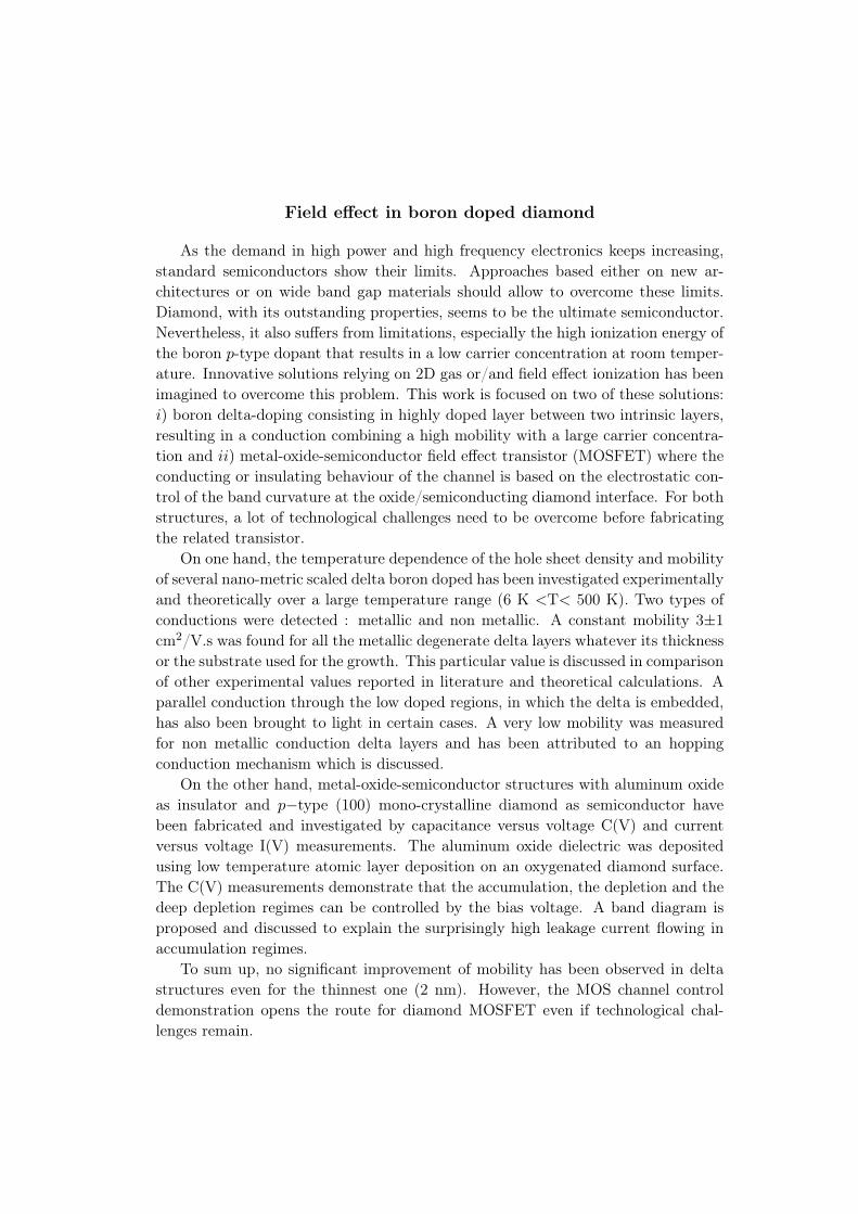
Field effect in boron doped diamond
As the demand in high power and high frequency electronics keeps increasing,
standard semiconductors show their limits. Approaches based either on new ar-
chitectures or on wide band gap materials should allow to overcome these limits.
Diamond, with its outstanding properties, seems to be the ultimate semiconductor.
Nevertheless, it also suffers from limitations, especially the high ionization energy of
the boron p-type dopant that results in a low carrier concentration at room temper-
ature. Innovative solutions relying on 2D gas or/and field effect ionization has been
imagined to overcome this problem. This work is focused on two of these solutions:
i) boron delta-doping consisting in highly doped layer between two intrinsic layers,
resulting in a conduction combining a high mobility with a large carrier concentra-
tion and ii) metal-oxide-semiconductor field effect transistor (MOSFET) where the
conducting or insulating behaviour of the channel is based on the electrostatic con-
trol of the band curvature at the oxide/semiconducting diamond interface. For both
structures, a lot of technological challenges need to be overcome before fabricating
the related transistor.
On one hand, the temperature dependence of the hole sheet density and mobility
of several nano-metric scaled delta boron doped has been investigated experimentally
and theoretically over a large temperature range (6 K <T< 500 K). Two types of
conductions were detected : metallic and non metallic. A constant mobility 3±1
cm2/V.s was found for all the metallic degenerate delta layers whatever its thickness
or the substrate used for the growth. This particular value is discussed in comparison
of other experimental values reported in literature and theoretical calculations. A
parallel conduction through the low doped regions, in which the delta is embedded,
has also been brought to light in certain cases. A very low mobility was measured
for non metallic conduction delta layers and has been attributed to an hopping
conduction mechanism which is discussed.
On the other hand, metal-oxide-semiconductor structures with aluminum oxide
as insulator and p−type (100) mono-crystalline diamond as semiconductor have
been fabricated and investigated by capacitance versus voltage C(V) and current
versus voltage I(V) measurements. The aluminum oxide dielectric was deposited
using low temperature atomic layer deposition on an oxygenated diamond surface.
The C(V) measurements demonstrate that the accumulation, the depletion and the
deep depletion regimes can be controlled by the bias voltage. A band diagram is
proposed and discussed to explain the surprisingly high leakage current flowing in
accumulation regimes.
To sum up, no significant improvement of mobility has been observed in delta
structures even for the thinnest one (2 nm). However, the MOS channel control
demonstration opens the route for diamond MOSFET even if technological chal-
lenges remain.