Resonant Tunneling in Graphene Pseudomagnetic Quantum Dots
6
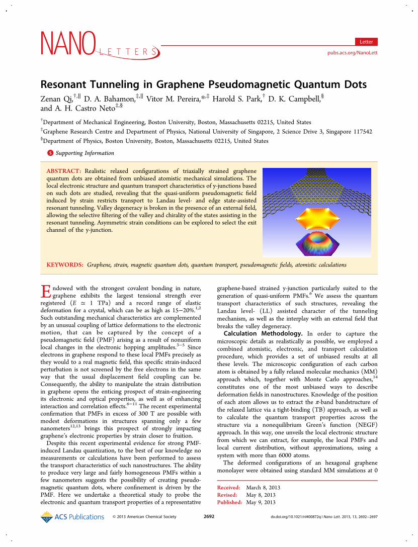
Resonant Tunneling in Graphene Pseudomagnetic Quantum Dots Zenan Qi, †,∥ D. A. Bahamon, ‡,∥ Vitor M. Pereira,* ,‡ Harold S. Park, † D. K. Campbell, § and A. H. Castro Neto ‡,§ † Department of Mechanical Engineering, Boston University, Boston, Massachusetts 02215, United States ‡ Graphene Research Centre and Department of Physics, National University of Singapore, 2 Science Drive 3, Singapore 117542 § Department of Physics, Boston University, Boston, Massachusetts 02215, United States * S Supporting Information ABSTRACT: Realistic relaxed configurations of triaxially strained graphene quantum dots are obtained from unbiased atomistic mechanical simulations. The local electronic structure and quantum transport characteristics of y-junctions based on such dots are studied, revealing that the quasi-uniform pseudomagnetic field induced by strain restricts transport to Landau level- and edge state-assisted resonant tunneling. Valley degeneracy is broken in the presence of an external field, allowing the selective filtering of the valley and chirality of the states assisting in the resonant tunneling. Asymmetric strain conditions can be explored to select the exit channel of the y-junction. KEYWORDS: Graphene, strain, magnetic quantum dots, quantum transport, pseudomagnetic fields, atomistic calculations E ndowed with the strongest covalent bonding in nature, graphene exhibits the largest tensional strength ever registered (E ≃ 1 TPa) and a record range of elastic deformation for a crystal, which can be as high as 15−20%. 1,2 Such outstanding mechanical characteristics are complemented by an unusual coupling of lattice deformations to the electronic motion, that can be captured by the concept of a pseudomagnetic field (PMF) arising as a result of nonuniform local changes in the electronic hopping amplitudes. 3−5 Since electrons in graphene respond to these local PMFs precisely as they would to a real magnetic field, this specific strain-induced perturbation is not screened by the free electrons in the same way that the usual displacement field coupling can be. Consequently, the ability to manipulate the strain distribution in graphene opens the enticing prospect of strain-engineering its electronic and optical properties, as well as of enhancing interaction and correlation effects. 6−11 The recent experimental confirmation that PMFs in excess of 300 T are possible with modest deformations in structures spanning only a few nanometers 12,13 brings this prospect of strongly impacting graphene’s electronic properties by strain closer to fruition. Despite this recent experimental evidence for strong PMF- induced Landau quantization, to the best of our knowledge no measurements or calculations have been performed to assess the transport characteristics of such nanostructures. The ability to produce very large and fairly homogeneous PMFs within a few nanometers suggests the possibility of creating pseudo- magnetic quantum dots, where confinement is driven by the PMF. Here we undertake a theoretical study to probe the electronic and quantum transport properties of a representative graphene-based strained y-junction particularly suited to the generation of quasi-uniform PMFs. 6 We assess the quantum transport characteristics of such structures, revealing the Landau level- (LL) assisted character of the tunneling mechanism, as well as the interplay with an external field that breaks the valley degeneracy. Calculation Methodology. In order to capture the microscopic details as realistically as possible, we employed a combined atomistic, electronic, and transport calculation procedure, which provides a set of unbiased results at all these levels. The microscopic configuration of each carbon atom is obtained by a fully relaxed molecular mechanics (MM) approach which, together with Monte Carlo approaches, 14 constitutes one of the most unbiased ways to describe deformation fields in nanostructures. Knowledge of the position of each atom allows us to extract the π-band bandstructure of the relaxed lattice via a tight-binding (TB) approach, as well as to calculate the quantum transport properties across the structure via a nonequilibrium Green’s function (NEGF) approach. In this way, one unveils the local electronic structure from which we can extract, for example, the local PMFs and local current distribution, without approximations, using a system with more than 6000 atoms. The deformed configurations of an hexagonal graphene monolayer were obtained using standard MM simulations at 0 Received: March 8, 2013 Revised: May 8, 2013 Published: May 9, 2013 Letter pubs.acs.org/NanoLett © 2013 American Chemical Society 2692 dx.doi.org/10.1021/nl400872q | Nano Lett. 2013, 13, 2692−2697
-
Upload
independent -
Category
Documents
-
view
0 -
download
0
Transcript of Resonant Tunneling in Graphene Pseudomagnetic Quantum Dots
Resonant Tunneling in Graphene Pseudomagnetic Quantum DotsZenan Qi,†,∥ D. A. Bahamon,‡,∥ Vitor M. Pereira,*,‡ Harold S. Park,† D. K. Campbell,§
and A. H. Castro Neto‡,§
†Department of Mechanical Engineering, Boston University, Boston, Massachusetts 02215, United States‡Graphene Research Centre and Department of Physics, National University of Singapore, 2 Science Drive 3, Singapore 117542§Department of Physics, Boston University, Boston, Massachusetts 02215, United States
*S Supporting Information
ABSTRACT: Realistic relaxed configurations of triaxially strained graphenequantum dots are obtained from unbiased atomistic mechanical simulations. Thelocal electronic structure and quantum transport characteristics of y-junctions basedon such dots are studied, revealing that the quasi-uniform pseudomagnetic fieldinduced by strain restricts transport to Landau level- and edge state-assistedresonant tunneling. Valley degeneracy is broken in the presence of an external field,allowing the selective filtering of the valley and chirality of the states assisting in theresonant tunneling. Asymmetric strain conditions can be explored to select the exitchannel of the y-junction.
KEYWORDS: Graphene, strain, magnetic quantum dots, quantum transport, pseudomagnetic fields, atomistic calculations
Endowed with the strongest covalent bonding in nature,graphene exhibits the largest tensional strength ever
registered (E ≃ 1 TPa) and a record range of elasticdeformation for a crystal, which can be as high as 15−20%.1,2Such outstanding mechanical characteristics are complementedby an unusual coupling of lattice deformations to the electronicmotion, that can be captured by the concept of apseudomagnetic field (PMF) arising as a result of nonuniformlocal changes in the electronic hopping amplitudes.3−5 Sinceelectrons in graphene respond to these local PMFs precisely asthey would to a real magnetic field, this specific strain-inducedperturbation is not screened by the free electrons in the sameway that the usual displacement field coupling can be.Consequently, the ability to manipulate the strain distributionin graphene opens the enticing prospect of strain-engineeringits electronic and optical properties, as well as of enhancinginteraction and correlation effects.6−11 The recent experimentalconfirmation that PMFs in excess of 300 T are possible withmodest deformations in structures spanning only a fewnanometers12,13 brings this prospect of strongly impactinggraphene’s electronic properties by strain closer to fruition.Despite this recent experimental evidence for strong PMF-
induced Landau quantization, to the best of our knowledge nomeasurements or calculations have been performed to assessthe transport characteristics of such nanostructures. The abilityto produce very large and fairly homogeneous PMFs within afew nanometers suggests the possibility of creating pseudo-magnetic quantum dots, where confinement is driven by thePMF. Here we undertake a theoretical study to probe theelectronic and quantum transport properties of a representative
graphene-based strained y-junction particularly suited to thegeneration of quasi-uniform PMFs.6 We assess the quantumtransport characteristics of such structures, revealing theLandau level- (LL) assisted character of the tunnelingmechanism, as well as the interplay with an external field thatbreaks the valley degeneracy.
Calculation Methodology. In order to capture themicroscopic details as realistically as possible, we employed acombined atomistic, electronic, and transport calculationprocedure, which provides a set of unbiased results at allthese levels. The microscopic configuration of each carbonatom is obtained by a fully relaxed molecular mechanics (MM)approach which, together with Monte Carlo approaches,14
constitutes one of the most unbiased ways to describedeformation fields in nanostructures. Knowledge of the positionof each atom allows us to extract the π-band bandstructure ofthe relaxed lattice via a tight-binding (TB) approach, as well asto calculate the quantum transport properties across thestructure via a nonequilibrium Green’s function (NEGF)approach. In this way, one unveils the local electronic structurefrom which we can extract, for example, the local PMFs andlocal current distribution, without approximations, using asystem with more than 6000 atoms.The deformed configurations of an hexagonal graphene
monolayer were obtained using standard MM simulations at 0
Received: March 8, 2013Revised: May 8, 2013Published: May 9, 2013
Letter
pubs.acs.org/NanoLett
© 2013 American Chemical Society 2692 dx.doi.org/10.1021/nl400872q | Nano Lett. 2013, 13, 2692−2697
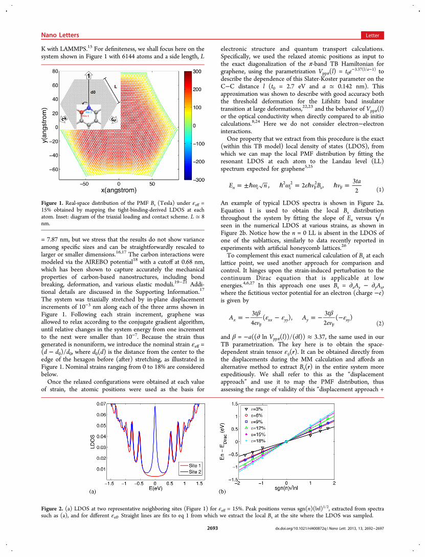
K with LAMMPS.15 For definiteness, we shall focus here on thesystem shown in Figure 1 with 6144 atoms and a side length, L
= 7.87 nm, but we stress that the results do not show varianceamong specific sizes and can be straightforwardly rescaled tolarger or smaller dimensions.16,17 The carbon interactions weremodeled via the AIREBO potential18 with a cutoff at 0.68 nm,which has been shown to capture accurately the mechanicalproperties of carbon-based nanostructures, including bondbreaking, deformation, and various elastic moduli.19−21 Addi-tional details are discussed in the Supporting Information.17
The system was triaxially stretched by in-plane displacementincrements of 10−3 nm along each of the three arms shown inFigure 1. Following each strain increment, graphene wasallowed to relax according to the conjugate gradient algorithm,until relative changes in the system energy from one incrementto the next were smaller than 10−7. Because the strain thusgenerated is nonuniform, we introduce the nominal strain εeff =(d − d0)/d0, where d0(d) is the distance from the center to theedge of the hexagon before (after) stretching, as illustrated inFigure 1. Nominal strains ranging from 0 to 18% are consideredbelow.Once the relaxed configurations were obtained at each value
of strain, the atomic positions were used as the basis for
electronic structure and quantum transport calculations.Specifically, we used the relaxed atomic positions as input tothe exact diagonalization of the π-band TB Hamiltonian forgraphene, using the parametrization Vppπ(l) = t0e
−3.37(l/a−1) todescribe the dependence of this Slater-Koster parameter on theC−C distance l (t0 = 2.7 eV and a ≃ 0.142 nm). Thisapproximation was shown to describe with good accuracy boththe threshold deformation for the Lifshitz band insulatortransition at large deformations,22,23 and the behavior of Vppπ(l)or the optical conductivity when directly compared to ab initiocalculations.8,24 Here we do not consider electron−electroninteractions.One property that we extract from this procedure is the exact
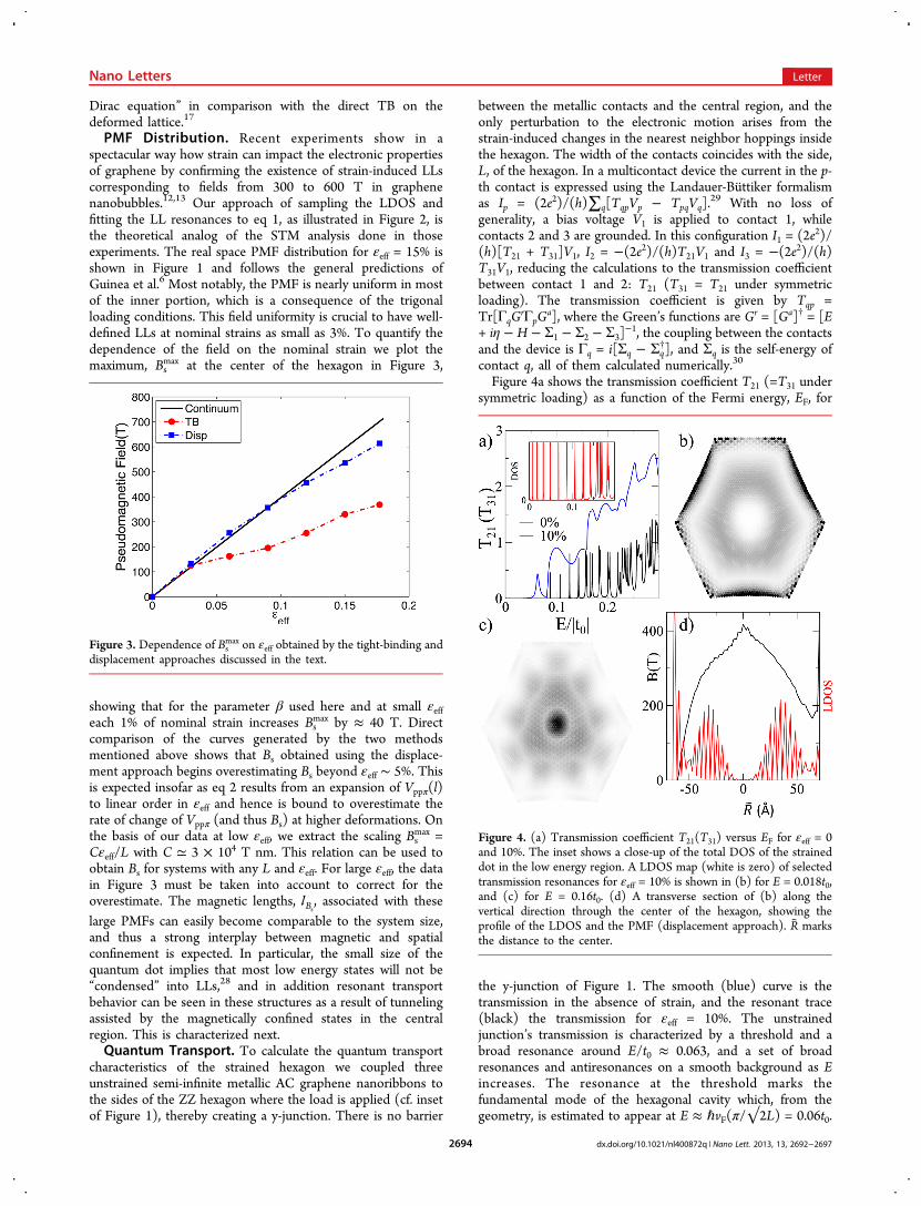
(within this TB model) local density of states (LDOS), fromwhich we can map the local PMF distribution by fitting theresonant LDOS at each atom to the Landau level (LL)spectrum expected for graphene5,25
ω ω= ±ℏ ℏ = ℏ ℏ =E n e v B vta
, 2 ,32n c
2c2
F2
s F (1)
An example of typical LDOS spectra is shown in Figure 2a.Equation 1 is used to obtain the local Bs distributionthroughout the system by fitting the slope of En versus √nseen in the numerical LDOS at various strains, as shown inFigure 2b. Notice how the n = 0 LL is absent in the LDOS ofone of the sublattices, similarly to data recently reported inexperiments with artificial honeycomb lattices.26
To complement this exact numerical calculation of Bs at eachlattice point, we used another approach for comparison andcontrol. It hinges upon the strain-induced perturbation to thecontinuum Dirac equation that is applicable at lowenergies.4,6,27 In this approach one uses Bs = ∂xAy − ∂yAx,where the fictitious vector potential for an electron (charge −e)is given by
β ε ε β ε= − − = − −Atev
Atev
34
( ),32
( )x xx yy y xyF F (2)
and β = −a((∂ ln Vppπ(l))/(∂l)) ≈ 3.37, the same used in ourTB parametrization. The key here is to obtain the space-dependent strain tensor εij(r). It can be obtained directly fromthe displacements during the MM calculation and affords analternative method to extract Bs(r) in the entire system moreexpeditiously. We shall refer to this as the “displacementapproach” and use it to map the PMF distribution, thusassessing the range of validity of this “displacement approach +
Figure 1. Real-space distribution of the PMF Bs (Tesla) under εeff =15% obtained by mapping the tight-binding-derived LDOS at eachatom. Inset: diagram of the triaxial loading and contact scheme. L ≃ 8nm.
Figure 2. (a) LDOS at two representative neighboring sites (Figure 1) for εeff = 15%. Peak positions versus sgn(n)(|n|)1/2, extracted from spectrasuch as (a), and for different εeff. Straight lines are fits to eq 1 from which we extract the local Bs at the site where the LDOS was sampled.
Nano Letters Letter
dx.doi.org/10.1021/nl400872q | Nano Lett. 2013, 13, 2692−26972693
Dirac equation” in comparison with the direct TB on thedeformed lattice.17
PMF Distribution. Recent experiments show in aspectacular way how strain can impact the electronic propertiesof graphene by confirming the existence of strain-induced LLscorresponding to fields from 300 to 600 T in graphenenanobubbles.12,13 Our approach of sampling the LDOS andfitting the LL resonances to eq 1, as illustrated in Figure 2, isthe theoretical analog of the STM analysis done in thoseexperiments. The real space PMF distribution for εeff = 15% isshown in Figure 1 and follows the general predictions ofGuinea et al.6 Most notably, the PMF is nearly uniform in mostof the inner portion, which is a consequence of the trigonalloading conditions. This field uniformity is crucial to have well-defined LLs at nominal strains as small as 3%. To quantify thedependence of the field on the nominal strain we plot themaximum, Bs
max at the center of the hexagon in Figure 3,
showing that for the parameter β used here and at small εeffeach 1% of nominal strain increases Bs
max by ≈ 40 T. Directcomparison of the curves generated by the two methodsmentioned above shows that Bs obtained using the displace-ment approach begins overestimating Bs beyond εeff ∼ 5%. Thisis expected insofar as eq 2 results from an expansion of Vppπ(l)to linear order in εeff and hence is bound to overestimate therate of change of Vppπ (and thus Bs) at higher deformations. Onthe basis of our data at low εeff, we extract the scaling Bs
max =Cεeff/L with C ≃ 3 × 10⁴ T nm. This relation can be used toobtain Bs for systems with any L and εeff. For large εeff, the datain Figure 3 must be taken into account to correct for theoverestimate. The magnetic lengths, Bs
, associated with theselarge PMFs can easily become comparable to the system size,and thus a strong interplay between magnetic and spatialconfinement is expected. In particular, the small size of thequantum dot implies that most low energy states will not be“condensed” into LLs,28 and in addition resonant transportbehavior can be seen in these structures as a result of tunnelingassisted by the magnetically confined states in the centralregion. This is characterized next.Quantum Transport. To calculate the quantum transport
characteristics of the strained hexagon we coupled threeunstrained semi-infinite metallic AC graphene nanoribbons tothe sides of the ZZ hexagon where the load is applied (cf. insetof Figure 1), thereby creating a y-junction. There is no barrier
between the metallic contacts and the central region, and theonly perturbation to the electronic motion arises from thestrain-induced changes in the nearest neighbor hoppings insidethe hexagon. The width of the contacts coincides with the side,L, of the hexagon. In a multicontact device the current in the p-th contact is expressed using the Landauer-Buttiker formalismas Ip = (2e2)/(h)∑q[TqpVp − TpqVq].
29 With no loss ofgenerality, a bias voltage V1 is applied to contact 1, whilecontacts 2 and 3 are grounded. In this configuration I1 = (2e2)/(h)[T21 + T31]V1, I2 = −(2e2)/(h)T21V1 and I3 = −(2e2)/(h)T31V1, reducing the calculations to the transmission coefficientbetween contact 1 and 2: T21 (T31 = T21 under symmetricloading). The transmission coefficient is given by Tqp =Tr[ΓqG
rΓpGa], where the Green’s functions are Gr = [Ga]† = [E
+ iη − H − Σ1 − Σ2 − Σ3]−1, the coupling between the contacts
and the device is Γq = i[Σq − Σq†], and Σq is the self-energy of
contact q, all of them calculated numerically.30
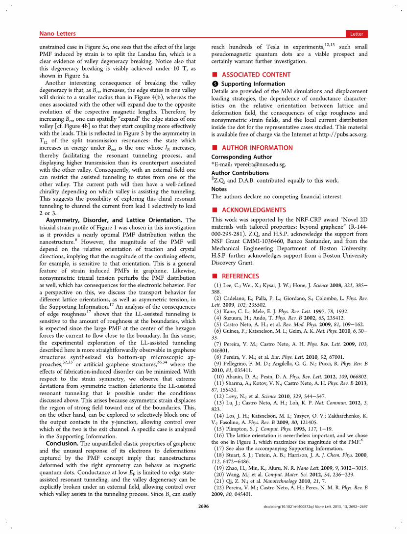
Figure 4a shows the transmission coefficient T21 (=T31 undersymmetric loading) as a function of the Fermi energy, EF, for
the y-junction of Figure 1. The smooth (blue) curve is thetransmission in the absence of strain, and the resonant trace(black) the transmission for εeff = 10%. The unstrainedjunction’s transmission is characterized by a threshold and abroad resonance around E/t0 ≈ 0.063, and a set of broadresonances and antiresonances on a smooth background as Eincreases. The resonance at the threshold marks thefundamental mode of the hexagonal cavity which, from thegeometry, is estimated to appear at E ≈ ℏvF(π/√2L) = 0.06t0.
Figure 3. Dependence of Bsmax on εeff obtained by the tight-binding and
displacement approaches discussed in the text.
Figure 4. (a) Transmission coefficient T21(T31) versus EF for εeff = 0and 10%. The inset shows a close-up of the total DOS of the straineddot in the low energy region. A LDOS map (white is zero) of selectedtransmission resonances for εeff = 10% is shown in (b) for E = 0.018t0,and (c) for E = 0.16t0. (d) A transverse section of (b) along thevertical direction through the center of the hexagon, showing theprofile of the LDOS and the PMF (displacement approach). R marksthe distance to the center.
Nano Letters Letter
dx.doi.org/10.1021/nl400872q | Nano Lett. 2013, 13, 2692−26972694

Spatial mapping of the LDOS (not shown) at this energyconfirms this.Upon stretching, the following three different regions can be
identified in the curve of T21(E) in Figure 4a: (i) at lowenergies the transmission is suppressed; (ii) at intermediateenergies the transmission develops a series of regularly spacedsharp resonances; and (iii) at higher energies the transmissionshows unevenly spaced and rapidly oscillating peaks. Tocharacterize these different regimes we resort to the features ofthe overall DOS, as well as the LDOS distribution, N(r,E) =(−1/π) Im[Gr(r,r;E)], at representative energies. The DOS isshown in the inset of Figure 4a and, even though there areplenty of low energy states, only those above E ≈ 0.08 t0 havean appreciable signature in the transmission. To understandthis absence of transmission we turn to Figure 4b, which plots areal-space LDOS map of a state at E = 0.018t0, representative ofthese low energy states that have no signature in thetransmission. Apart from the nonpropagating LDOS accumu-lation at the ZZ edges, the significant LDOS amplitude isdistributed within an annulus of radius ≈4 nm and width ≈2.5nm. Since the LDOS does not extend to the vicinity of thecontacts, revealing a small coupling between this state and themodes of the contacts, the only possibility for transmission isthrough tunneling. But since the spatial barrier for tunnelinginto this confined state is rather large (≈2.5 nm), the resonantpeak in the transmission associated with this state has avanishingly small amplitude and is not seen on the scale ofFigure 4. A transverse cut of the LDOS in Figure 4b along thevertical direction through the hexagon center is shown inFigure 4 panel d.17 It reflects the wave function of a PMF-induced Landau edge state confined to the hexagonal quantumdot, analogous to the edge states in magnetic quantum dots.28
As the energy is progressively increased, the associated statesspread out, approaching the boundaries. Their coupling to thecontacts increases until the tunneling-assisted conductancebecomes of the order of the conductance quantum and theassociated transmission resonances become visible in the blacktrace of Figure 4b.The LDOS map in Figure 4c corresponds to E = 0.16t0 and
typifies the behavior at higher EF. It is clear that this state iscompletely different from the one in Figure 4b, as its LDOSspreads over the entire dot and is highly peaked at the center. Itcorresponds to a state in the n = 1 LL. The rapid oscillations inthe transmission coefficient and DOS at that energy are alsoconsistent with this interpretation.31 An additional quantitativeconfirmation is given as follows. If the state at E = 0.16t0belongs to the n = 1 LL, its associated magnetic length will beBs= √2ℏvF/En=1 ≃ 1.9 nm. The energy difference between
Landau edge states whose energy is between En=0 and En=1 canbe estimated by dividing the LL separation by the number ofedge states per LL: ΔE ≈ (En=1 − En=0) Bs
/2L0 ≈ 0.02t0, where
the factor L2 / B0 scorresponds to the average number of edge
states between these two Landau levels.31 Inspecting the insetof Figure 4a we verify that the level spacing below E ≃ 0.1t0 isindeed ∼0.02t0. Moreover, given that this quantitative estimateis consistent, we can extract the average magnetic fielddetermining the transport behavior, which is Bs
av = ℏ/e B2
s≃
164 T. This value, obtained independently and solely from thetransmission characteristics, expectedly corresponds to thePMF in the region of maximum LDOS for this state, fromFigure 4d and, correcting for the overestimation in the PMFs
obtained from the displacement approach in Figure 3, thatwould be ≈270/1.6 = 169 T.Hence, transport in the strained junction is characterized by
LL-assisted resonant tunneling, analogously to a magneticquantum dot, with the novelty that here the Landauquantization arises from the strain-induced PMF, Bs. Becauseof the effective magnetic barrier, electrons injected from contact1 can tunnel with a probability 0 < T < 1, which is enhancedwhen there is significant LDOS in the contact region. Themaximum tunneling probability through a localized state is T =1, irrespective of the number of open channels in the contacts.This implies that between the LL n = 0 and n = 1 we expectT21max = 0.5 (0.5 because there are two symmetric exit channels).
However each LL with n ≠ 0 in graphene is doubly degenerate,and hence T21
max = 1, which is consistent with the calculatedtransmission seen in Figure 4a, where T21(E = 0.126t0) = 0.79,for example.
Valley Splitting. The strain-induced PMF does not breaktime-reversal symmetry (TRS) in the system, which in practicemeans that a low energy electron around one of the zone-edgevalleys feels a PMF which is exactly the opposite to the one feltby its TRS counterpart at the other inequivalent valley. Thisleads to the degeneracy discussed above and, in addition, to theresult that the currents associated with the two valleys exactlycancel each other. This degeneracy is lifted under a realmagnetic field, Bext, since the total field at each valley will bedifferent: Bext ± Bs. The corresponding LL splitting is given byEn+ − En
− ≃ EnBext/Bsav. In Figure 5a, we show explicitly this
splitting for the edge states detached from the n = 1 LL. Takingthe values estimated above for Bs
av ≃ 164 T, and En=1 ≃ 0.16t0,the expected splitting under the external field is (E+ − E−)/t0 ≃0.001BextT
−1. Direct inspection of Figure 5a shows that this isindeed quantitatively verified. A different perspective over thesplitting of valley degeneracy is given in Figure 5b, which showsthe spectrum of the strained hexagon disconnected from thecontacts, as a function of Bext. When compared with the
Figure 5. (a) Detail of the splitting in the T21 resonances under anexternal field Bext, for εeff = 10%. (b) Eigenenergies of the samehexagon versus Bext, when disconnected from the contacts. (c)Likewise but for εeff = 0, where LL condensation28 is more clearlyobserved. In (b,c), straight lines mark the lowest LLs in the infinitesystem, and the large range of Bext used in the horizontal axes is toaccommodate the very large PMF induced by strain.
Nano Letters Letter
dx.doi.org/10.1021/nl400872q | Nano Lett. 2013, 13, 2692−26972695
unstrained case in Figure 5c, one sees that the effect of the largePMF induced by strain is to split the Landau fan, which is aclear evidence of valley degeneracy breaking. Notice also thatthis degeneracy breaking is visibly achieved under 10 T, asshown in Figure 5a.Another interesting consequence of breaking the valley
degeneracy is that, as Bext increases, the edge states in one valleywill shrink to a smaller radius than in Figure 4(b), whereas theones associated with the other will expand due to the oppositeevolution of the respective magnetic lengths. Therefore, byincreasing Bext one can spatially “expand” the edge states of onevalley [cf. Figure 4b] so that they start coupling more effectivelywith the leads. This is reflected in Figure 5 by the asymmetry inT12 of the split transmission resonances: the state whichincreases in energy under Bext is the one whose B increases,thereby facilitating the resonant tunneling process, anddisplaying higher transmission than its counterpart associatedwith the other valley. Consequently, with an external field onecan restrict the assisted tunneling to states from one or theother valley. The current path will then have a well-definedchirality depending on which valley is assisting the tunneling.This suggests the possibility of exploring this chiral resonanttunneling to channel the current from lead 1 selectively to lead2 or 3.Asymmetry, Disorder, and Lattice Orientation. The
triaxial strain profile of Figure 1 was chosen in this investigationas it provides a nearly optimal PMF distribution within thenanostructure.6 However, the magnitude of the PMF willdepend on the relative orientation of traction and crystaldirections, implying that the magnitude of the confining effects,for example, is sensitive to that orientation. This is a generalfeature of strain induced PMFs in graphene. Likewise,nonsymmetric triaxial tension perturbs the PMF distributionas well, which has consequences for the electronic behavior. Fora perspective on this, we discuss the transport behavior fordifferent lattice orientations, as well as asymmetric tension, inthe Supporting Information.17 An analysis of the consequencesof edge roughness17 shows that the LL-assisted tunneling issensitive to the amount of roughness at the boundaries, whichis expected since the large PMF at the center of the hexagonforces the current to flow close to the boundary. In this sense,the experimental exploration of the LL-assisted tunnelingdescribed here is more straightforwardly observable in graphenestructures synthesized via bottom-up microscopic ap-proaches,32,33 or artificial graphene structures,26,34 where theeffects of fabrication-induced disorder can be minimized. Withrespect to the strain symmetry, we observe that extremedeviations from symmetric traction deteriorate the LL-assistedresonant tunneling that is possible under the conditionsdiscussed above. This arises because asymmetric strain displacesthe region of strong field toward one of the boundaries. This,on the other hand, can be explored to selectively block one ofthe output contacts in the y-junction, allowing control overwhich of the two is the exit channel. A specific case is analyzedin the Supporting Information.Conclusion. The unparalleled elastic properties of graphene
and the unusual response of its electrons to deformationscaptured by the PMF concept imply that nanostructuresdeformed with the right symmetry can behave as magneticquantum dots. Conductance at low EF is limited to edge state-assisted resonant tunneling, and the valley degeneracy can beexplicitly broken under an external field, allowing control overwhich valley assists in the tunneling process. Since Bs can easily
reach hundreds of Tesla in experiments,12,13 such smallpseudomagnetic quantum dots are a viable prospect andcertainly warrant further investigation.
■ ASSOCIATED CONTENT*S Supporting InformationDetails are provided of the MM simulations and displacementloading strategies, the dependence of conductance character-istics on the relative orientation between lattice anddeformation field, the consequences of edge roughness andnonsymmetric strain fields, and the local current distributioninside the dot for the representative cases studied. This materialis available free of charge via the Internet at http://pubs.acs.org.
■ AUTHOR INFORMATIONCorresponding Author*E-mail: [email protected] Contributions∥Z.Q. and D.A.B. contributed equally to this work.NotesThe authors declare no competing financial interest.
■ ACKNOWLEDGMENTSThis work was supported by the NRF-CRP award “Novel 2Dmaterials with tailored properties: beyond graphene” (R-144-000-295-281). Z.Q. and H.S.P. acknowledge the support fromNSF Grant CMMI-1036460, Banco Santander, and from theMechanical Engineering Department of Boston University.H.S.P. further acknowledges support from a Boston UniversityDiscovery Grant.
■ REFERENCES(1) Lee, C.; Wei, X.; Kysar, J. W.; Hone, J. Science 2008, 321, 385−388.(2) Cadelano, E.; Palla, P. L.; Giordano, S.; Colombo, L. Phys. Rev.Lett. 2009, 102, 235502.(3) Kane, C. L.; Mele, E. J. Phys. Rev. Lett. 1997, 78, 1932.(4) Suzuura, H.; Ando, T. Phys. Rev. B 2002, 65, 235412.(5) Castro Neto, A. H.; et al. Rev. Mod. Phys. 2009, 81, 109−162.(6) Guinea, F.; Katsnelson, M. I.; Geim, A. K. Nat. Phys. 2010, 6, 30−33.(7) Pereira, V. M.; Castro Neto, A. H. Phys. Rev. Lett. 2009, 103,046801.(8) Pereira, V. M.; et al. Eur. Phys. Lett. 2010, 92, 67001.(9) Pellegrino, F. M. D.; Angilella, G. G. N.; Pucci, R. Phys. Rev. B2010, 81, 035411.(10) Abanin, D. A.; Pesin, D. A. Phys. Rev. Lett. 2012, 109, 066802.(11) Sharma, A.; Kotov, V. N.; Castro Neto, A. H. Phys. Rev. B 2013,87, 155431.(12) Levy, N.; et al. Science 2010, 329, 544−547.(13) Lu, J.; Castro Neto, A. H.; Loh, K. P. Nat. Commun. 2012, 3,823.(14) Los, J. H.; Katsnelson, M. I.; Yazyev, O. V.; Zakharchenko, K.V.; Fasolino, A. Phys. Rev. B 2009, 80, 121405.(15) Plimpton, S. J. Comput. Phys. 1995, 117, 1−19.(16) The lattice orientation is nevertheless important, and we chosethe one in Figure 1, which maximizes the magnitude of the PMF.6
(17) See also the accompanying Supporting Information.(18) Stuart, S. J.; Tutein, A. B.; Harrison, J. A. J. Chem. Phys. 2000,112, 6472−6486.(19) Zhao, H.; Min, K.; Aluru, N. R. Nano Lett. 2009, 9, 3012−3015.(20) Wang, M.; et al. Comput. Mater. Sci. 2012, 54, 236−239.(21) Qi, Z. N.; et al. Nanotechnology 2010, 21, 7.(22) Pereira, V. M.; Castro Neto, A. H.; Peres, N. M. R. Phys. Rev. B2009, 80, 045401.
Nano Letters Letter
dx.doi.org/10.1021/nl400872q | Nano Lett. 2013, 13, 2692−26972696

(23) Ni, Z. H.; et al. ACS Nano 2009, 3, 483.(24) Ribeiro, R. M.; et al. New J. Phys. 2009, 11, 115002.(25) McClure, J. W. Phys. Rev. 1956, 104, 666.(26) Gomes, K. K.; et al. Nature 2012, 483, 306−310.(27) Vozmediano, M. A. H.; Katsnelson, M. I.; Guinea, F. Phys. Rep.2010, 496, 109−148.(28) Lent, C. S. Phys. Rev. B 1991, 43, 4179−4186.(29) Datta, S. Electronic Transport in Mesoscopic Systems; CambridgeUniversity Press: New York, 1995.(30) Bahamon, D. A.; Pereira, A. L. C.; Schulz, P. A. Phys. Rev. B2010, 82, 165438.(31) Sivan, U.; Imry, Y.; Hartzstein, C. Phys. Rev. B 1989, 39, 1242−1250.(32) Zhi, L.; Mullen, K. J. Mater. Chem. 2008, 18, 1472.(33) Cai, J.; et al. Nature 2010, 466, 470.(34) Park, C.-H.; Louie, S. G. Nano Lett. 2009, 9, 1793.
Nano Letters Letter
dx.doi.org/10.1021/nl400872q | Nano Lett. 2013, 13, 2692−26972697