Doping magnesiumiontotuneelectricalanddielectric properties ofBaCo2 hexaferrites
Sublattice asymmetry of impurity doping ingraphene: A review
James A. LawlorSchool of Physics, Trinity College Dublin, Dublin 2, Ireland
Mauro S. FerreiraSchool of Physics, Trinity College Dublin, Dublin 2, Ireland
CRANN, Trinity College Dublin, Dublin 2, Ireland
July 10, 2014
Abstract
In this review we highlight recent theoretical and experimentalwork on sublattice asymmetric doping of impurities in graphene, witha focus on substitutional Nitrogen dopants. It is well known that onecurrent limitation of graphene in regards to its use in electronics isthat in its ordinary state it exhibits no band gap. By doping oneof its two sublattices preferentially it is possible to not only opensuch a gap, which can furthermore be tuned through control of thedopant concentration, but in theory produce quasi-ballistic transportof electrons in the undoped sublattice, both important qualities for anygraphene device to be used competetively in future technology. Weoutline current experimental techniques for synthesis of such graphenemonolayers and detail theoretical efforts to explain the mechanismsresponsible for the effect, before suggesting future research directionsin this nascent field.
1
arX
iv:1
407.
2560
v1 [
cond
-mat
.mes
-hal
l] 9
Jul
201
4

1 Review
1.1 Introduction
With its excellent transport properties and low dimensionality, graphene,an atomically thin layer of Carbon atoms bonded together in a hexagonallattice, initially seems a strong candidate for use in many future commer-cial applications such as ultra high-speed transistors, integrated circuits andother novel devices [15, 35, 8]. One of the main problems with using regulargraphene for such applications is the absence of a band gap in the electronicband structure [1], and as a result any Field Effect Transistors (FETs) madeusing the material (so-called GFETs) would be unable to be switched off,rendering it useless as a logic device [47, 29, 62]. The most natural way toapproach this issue is therefore to introduce a sizeable band gap and henceallowing more control over the current flow.
Although several methods exist to induce a band gap, for example 1Dquantum confinement by construction of graphene nanoribbons (GNRs) [28],stacking of monolayers with perpendicular electric fields [29, 62], strain [34]and mounting on a substrate [36, 65, 6], these methods are not withoutproblems. Alternatives are therefore sought after with the minimum standardto meet or exceed the limits of silicon semiconductor technology, which ischaracterised by a current on/off ratio of roughly 104-107 and a band gap ofat least 340meV whilst maintaining high carrier mobility [2, 47, 21].
Alteration of the crystal structure through the introduction of foreigndopants is one of the more realistic avenues of approach in realising thisgoal. Atomic dopants like Boron (B) or Nitrogen (N) are a similar size toCarbon and can be introduced easily in a variety of graphene growth pro-cesses, typically replacing Carbon sites and forming substitutional impuritiesin the lattice, positively (p-) and negatively (n-) doping the system for B andN dopants respectively [18]. Early theoretical attempts at investigating theelectronic properties of such a material found that a periodic arrangementof B or N dopants, forming a dopant superlattice, would open a band gap[5], but that a random distribution of dopants among lattice sites yields noband gap [26]. Further investigations using vacancies, where carbon atomsare removed from the lattice, found that both superlattices [32] and ran-dom distributions restricted to one of the two graphene sublattices [38] bothlead to a tunable band gap, and in the latter case an emergence of magneticproperties in the system [10, 41]. Whilst these findings are certainly interest-
2

ing, their scalability, and hence commercial application, is prohibited by thestandard of precision that must be met in order to produce such materials.Circumventing these problems using Nitrogen doped graphene has only comeabout relatively recently which we detail in the following section.
1.2 A Brief History of Nitrogen Doped Graphene
Exploiting the effects of Nitrogen dopants on the transport properties ofgraphene has been an interesting experimental research topic for the last 5years [58], whereby the methods and techniques to achieve this have beendeveloped to include Chemical Vapour Deposition (CVD), usingNH3as aprecursor, arc discharge [16], embedded nitrogen and carbon sources withina metal substrate [61], ion implantation [50, 3], Ammonia [30] or Nitrogenplasma [56, 19] treatments, and capable of achieving Nitrogen dopant con-centrations of up to around 10% [53] and with direct applicablity to GFETtechnology and bio-sensing [57]. Although CVD is one of the more challeng-ing methods, it seems the most reliable option and yields the best qualityNitrogen doped graphene sheets [54] and single continuous sheets can be syn-thesised on the centimeter scale [14]. Using Nitrogen dopants alone throughCVD can yield bandgaps up to 200meV [51] and by inclusion of Boron co-dopants, through a tailored growth process, this can be expanded to around600meV with 6% total dopant concentration [6]. Boron doping alone hasshown to also open a band gap, tunable with dopant concentration [49, 13].This method results in small B-N domains embedded in the graphene sheet,so the precise mechanism behind the band gap opening may not be the sameas that seen in a random B-N ensemble. Although these gaps are quite size-able, the effect of scattering would lead to a detrimental impact on the trans-port characteristics. However, the recent theoretical prediction of sublatticeasymmetry, a situation where dopants are distributed in one sublattice only,is expected to yield very low scattering transport properties. The electronwavefunctions in such a system are shown to mainly exist on the sublat-tice without dopants and can travel almost unhindered [27, 4], which is verypromising for overcoming the scattering problem.
It was not until 2011 that a viable experimental approach was found byZhao et al. [63]. They discovered that graphene grown via Chemical VapourDeposition (CVD) in the presence of ammonia (NH3) naturally incorporatesNitrogen atoms as substitutional so-called ’graphitic’ dopants (see Fig. 1A) into the crystal, and with a distinct sublattice segregation of dopants.
3
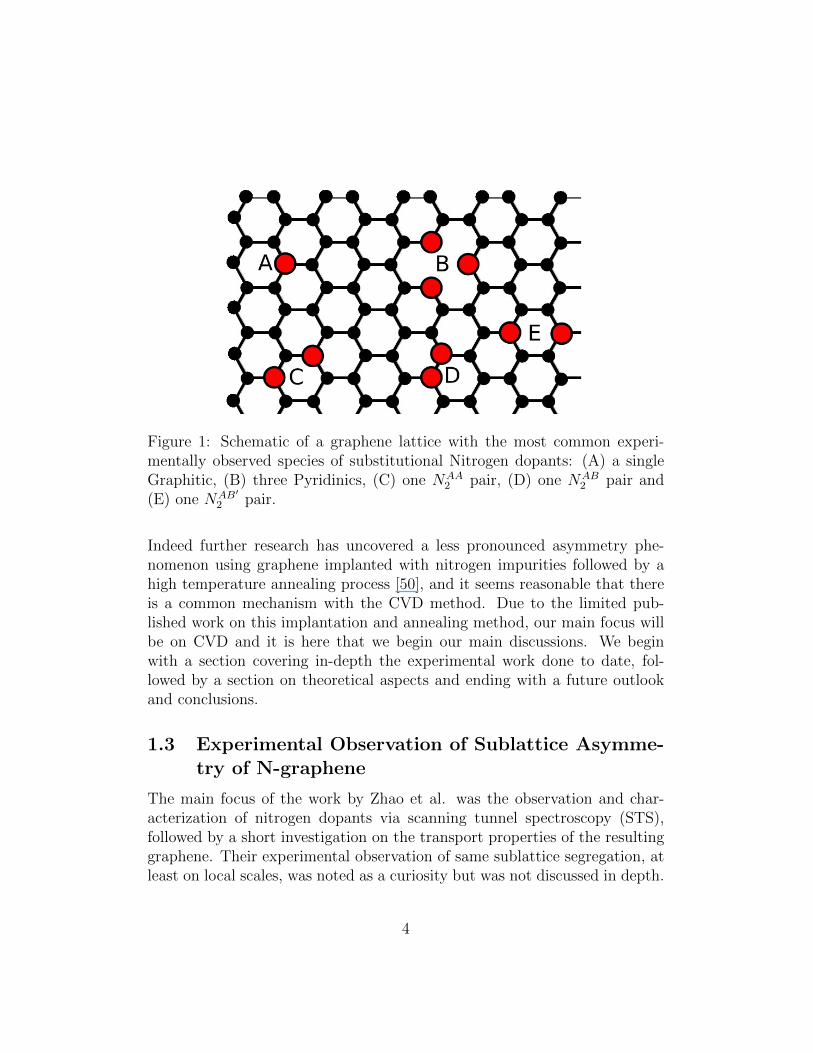
Figure 1: Schematic of a graphene lattice with the most common experi-mentally observed species of substitutional Nitrogen dopants: (A) a singleGraphitic, (B) three Pyridinics, (C) one NAA
2 pair, (D) one NAB2 pair and
(E) one NAB′2 pair.
Indeed further research has uncovered a less pronounced asymmetry phe-nomenon using graphene implanted with nitrogen impurities followed by ahigh temperature annealing process [50], and it seems reasonable that thereis a common mechanism with the CVD method. Due to the limited pub-lished work on this implantation and annealing method, our main focus willbe on CVD and it is here that we begin our main discussions. We beginwith a section covering in-depth the experimental work done to date, fol-lowed by a section on theoretical aspects and ending with a future outlookand conclusions.
1.3 Experimental Observation of Sublattice Asymme-try of N-graphene
The main focus of the work by Zhao et al. was the observation and char-acterization of nitrogen dopants via scanning tunnel spectroscopy (STS),followed by a short investigation on the transport properties of the resultinggraphene. Their experimental observation of same sublattice segregation, atleast on local scales, was noted as a curiosity but was not discussed in depth.
4

A key finding by the researchers was that by varying the ammonia precursorconcentration they could adjust the resulting embedded dopant concentra-tion. Further theoretical work confirmed that a tunable band gap would beobtainable using this method [27], and along with the findings of Zhao et al.this sparked further interest into this phenomenon. It should be noted thatthe experimental conditions were a high vacuum CVD process on a Cu (111)substrate with a temperature of 1000 ◦C, using CH4 and NH3 as grapheneand Nitrogen precursors respectively for 18 minutes reaction time achievinga dopant concentration of 0.3%.
Shortly after this work a more focussed investigation was undertaken byLv et al. [31]. They were able to replicate the findings of the first group andsynthesised large areas of N-doped monolayer graphene with the additionalfinding that by increasing the pressure in the growth phase from a highvacuum to atmospheric-pressure CVD would result in an abundance of so-called NAA
2 pairs [31] (see Fig. 1 (C)), which are thought to be a result of ahigher number of intermolecule collisions during formation. Using the samesubstrate and precursors, they were also able to find that a minimum reactiontime of 5 minutes and temperatures of 800C were optimum for the N-dopedgraphene synthesis and moreover it was found that singular Nitrogen dopantsare more frequently found for reaction times below 10 minutes with the ratioof NAA
2 to single N increasing with reaction time. The samples had a typicalconcentration of around 0.25% Nitrogen dopants.
More recently the addition of Boron dopants into the lattice and theireffects have been studied [64] using high vacuum CVD growth and addingB2H6 diborane instead of ammonia as the dopant precursor, achieving con-centrations on the order of 0.3%. The researchers compared B-doped andN-doped systems in detail and found no detectable sublattice asymmetry inthe case of B-doped systems and thus the dopants were distributed evenlybetween sublattices. The reason for this is thought to be due to a strong in-teraction between the Cu (111) substrate and the Boron impurity, in contrastto a very weak interaction with the substrate for Nitrogen impurities[64].
The most recent and thorough study of asymmetric Nitrogen dopants ingraphene is by Zabet-Khosousi et al. [60] who again used the CVD growthprocess but with a pyridine (C5H5N) precursor for the Nitrogen and grapheneinstead of the conventional ammonia/methane mix. Fig. 2 shows a ratherstriking STM image of a large area of N-doped graphene grown using thismethod, showing two clearly defined domains of different sublattice pref-erence where the sharp borders are thought to arise from terracing of the
5

substrate disrupting the asymmetry effect. The method was tailored to usea very smooth Cu (111) substrate and so they were able to achieve domainsizes far larger than previous efforts. Typical concentrations found with thismethod were around 0.2%, very similar to the previous ammonia/methanemethod which points to an equivalent growth mechanism. By comparing N-doped graphene systems synthesised with this method to other systems madevia Nitrogen ion bombardement and ammonia post-treatment of a pristinegraphene sheet, where no sublattice asymmetric configurations were found, itwas suggested that the sublattice asymmetry must be occuring during forma-tion of the graphene sheet. This is supported by the recent experiments usingion bombardement followed by high temperature annealing by Telychko etal. [50], where the impurities may be reconfiguring themselves locally duringcooling. This phenomenon is not seen without the annealing process [3].
The common elements of all the aforementioned experimental reports arethat they all use a Cu (111) substrate, all have reaction times exceeding10 minutes in a temperature range of 800-900 ◦C, and all have used eitherammonia or pyridine precursors to achieve concentrations of up to 0.3%. Areview of other methods for N-doped graphene synthesis finds no mentionof sublattice asymmetry [19, 53], it is known that this effect is mainly de-tectable through careful Scanning Tunnel Microscopy of large areas. Themost natural explanation for this lack of observation is then either that it isnot being observed due to simply not looking, or that sublattice asymmetryis not a very robust effect and therefore requires a careful choice of synthesisprocedure. Research into the mechanisms behind the phenomenon is there-fore paramount in answering this question and could shed light on whetherother methods or even dopant species are at all possible and this leads usnaturally to a review of the current theoretical models of the effect.
1.4 Theoretical Models of the Segregation Effect
It is clear that any degree of asymmetry between the two equivalent sub-lattices is the result of a symmetry breaking operation. Current theoreticalattempts to explain the sublattice asymmetry in the Nitrogen doping seenin the experiments discussed in the previous section suggest that the effectcomes from either the energetically preferable positioning of Nitrogen onthe graphene edge during the growth process [60, 11], where the symmetrybreaking effect is the edge structure, or from inter-impurity interactions inthe impurity ensemble [31, 25] where the symmetry is broken by the impuri-
6

Figure 2: STM images of nitrogen doped graphene on (a) 7nm2, (b) 20nm2
and (c) 100nm2 scales, adapted with permission from Zabet-Khosousi et al.[60]. Copyright 2014 American Chemical Society. The dopants locationsare identified by finding bright spots on the STM image, corresponding toslight perturbations in the positions of the neighbouring carbon atoms. Thedopant sublattice can be found through the orientation of the bright trianglefeatures, where opposite sublattices appear as mirror images of each other asdemonstrated in (a). The red and blue triangles in each subfigure correspondto impurities on the different sublattices. Part (c) best demonstrates thatalthough the distribution of dopants appears random, when their sublatticeis identified we see two very large domains appear with opposite sublatticesegregation. Shown at the bottom, off-center left of (c) is a white 10nmscalebar.
7

ties themselves. These models will hereafter be referred to as the edge growthand interaction models respectively.
The edge growth model suggests that during the growth phase the mostenergetically favourable position for a Nitrogen dopant being incorporatedinto a graphene edge would be that which leads to a same sublattice config-uration for all impurities in a domain. Through Density Functional Theory(DFT) calculations involving a graphene nanoribbon on a Cu(111) substrate,aiming to reproduce experimental conditions, a thorough investigation intothe energetic favourable position of single graphitic Nitrogens in the GNRwas undertaken and the energetic difference between placing the Nitrogenat one edge site over another on the opposite sublattice was found to be asubstantial 1.3eV. One drawback of this method is that one would expecttherefore that the clearly defined segregation domains seen experimentally(see Fig. 2 and [60]) would naturally fall in with the graphene grain bound-aries, but this has not been observed. The role of inter-impurity interactionshas been considered as an alternative, through both Tight Binding [25] andDFT [31, 17] formalisms, although with differing conclusions. The TightBinding method by Lawlor et al. [25] was part of a more in-depth theoreticalinvestigation, and suggests that a Friedel Oscillation-like perturbation in thelong-range inter-impurity interactions [23] arise from adding impurities tothe system, leading to a shift in the system’s Fermi energy. Such a mech-anism would explain both the non-commensurability between crystal grainboundaries and segregation domains, and would suggest why the alternativesynthesis method of nitrogen implantation followed by high temperature an-nealing also results in impurities preferring to occupy the same sublattice[50]. Furthermore, the authors predict that as a result of this interactionand the reduction in nearest neighbour distance with increasing concentra-tion, there exists a critical dopant concentration beyond which no sublatticeasymmetry would be observed, as the energetic minimum occurs when theimpurities are distributed evenly between sublattices. Although the exactvalue of this critical concentration is dependant on how the impurity is pa-rameterised within the tight binding regime, the authors predict it to liebetween 0.1 % and 0.8%. Comparing to the highest experimentally reporteddoping concentrations for samples with sublattice asymmetry (0.3%), it is ahope that further experiments can clarify whether such a critical concentra-tion exists. If the prediction of a critical concentration is accurate it wouldlimit the band gap of a segregated device to around 100meV [27]. This fig-ure, however, comes from matching Tight Binding and DFT band structure
8

results, a method which is known to systematically underestimate such bandgaps. Nevertheless, the band gap obtained can be expected to be much belowthat required for a GFET device.
In-depth DFT calculations by Hou et al. [17] found that the interactionsbetween nitrogen impurities are generally repulsive in nature. More specifi-cally, when the two impurities are placed close together the system energy isminimised for opposite sublattice configurations, with the exception of NAB
2
. This contradicts the experimental reports of Lv et al. [31] who foundan abundance of NAA
2 defects in their samples. A simplistic Tight Bindingapproach predicts that two identical impurities in close proximity to one an-other would indeed have an energetic minimum when both occupy the samesublattice [24], however this method ignores coulombic interaction which willbe dominant at close separations. Interestingly, the DFT approach of Lv etal. of such Nitrogen pairs finds that the lowest energy configuration wouldbe NAB′
2 (see Fig 1), approximately 0.3eV lower than that ofNAA2 . This ap-
pears to be in disagreement with experiments whereNAA2 is more commonly
found thanNAB′2 . As a final note their calculations have also shown that two
NAA2 pairs have a lower energy when they share the same sublattice, however
further studies have shown that the overall energy change resulting from anNAA
2 pair in the sheet is very high [11]. It is possible that these impuritiesalso come from edge growth, but the controllable presence of NAA
2 in nitro-gen ion implanted graphene [50] indicates again that this may not be the fullpicture as in this case the complete graphene sheet is already fabricated.
1.5 Predicted Electronic Properties
The earliest attempts to study Nitrogen dopants and their effect on thegraphene electronic properties were purely theoretical. Beginning with im-purity superlattices, this research preceded the experimental realistation ofNitrogen doped graphene. By introducing a controlled periodic arrangementof Boron and Nitrogen impurities a band gap was seen to open [5], and al-though such superlattice structures were not feasible on large-scale it wasfurther shown that a random distribution on one sublattice can also open agap [4]. Further DFT studies showed that the band gap will increase withdopant concentration [44, 27] and that a dopant level of over 8%, where im-purities are all on the same sublattice, will produce a band gap of around550meV far surpassing the minimum required for a CMOS [27, 21] and find-ing that the band gap scales with concentration to the power 3/4, as shown
9
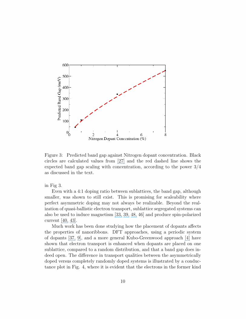
Figure 3: Predicted band gap against Nitrogen dopant concentration. Blackcircles are calculated values from [27] and the red dashed line shows theexpected band gap scaling with concentration, according to the power 3/4as discussed in the text.
in Fig 3.Even with a 4:1 doping ratio between sublattices, the band gap, although
smaller, was shown to still exist. This is promising for scaleability whereperfect asymmetric doping may not always be realizable. Beyond the real-ization of quasi-ballistic electron transport, sublattice segregated systems canalso be used to induce magnetism [33, 39, 48, 46] and produce spin-polarizedcurrent [40, 43].
Much work has been done studying how the placement of dopants affectsthe properties of nanoribbons. DFT approaches, using a periodic systemof dopants [37, 9], and a more general Kubo-Greenwood approach [4] haveshown that electron transport is enhanced when dopants are placed on onesublattice, compared to a random distribution, and that a band gap does in-deed open. The difference in transport qualities between the asymmetricallydoped versus completely randomly doped systems is illustrated by a conduc-tance plot in Fig. 4, where it is evident that the electrons in the former kind
10
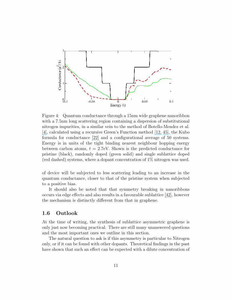
Figure 4: Quantum conductance through a 15nm wide graphene nanoribbonwith a 7.5nm long scattering region containing a dispersion of substitutionalnitrogen impurities, in a similar vein to the method of Botello-Mendez et al.[4], calculated using a recursive Green’s Function method [12, 45], the Kuboformula for conductance [22] and a configurational average of 50 systems.Energy is in units of the tight binding nearest neighbour hopping energybetween carbon atoms, t = 2.7eV. Shown is the predicted conductance forpristine (black), randomly doped (green solid) and single sublattice doped(red dashed) systems, where a dopant concentration of 1% nitrogen was used.
of device will be subjected to less scattering leading to an increase in thequantum conductance, closer to that of the pristine system when subjectedto a positive bias.
It should also be noted that that symmetry breaking in nanoribbonsoccurs via edge effects and also results in a favourable sublattice [42], howeverthe mechanism is distinctly different from that in graphene.
1.6 Outlook
At the time of writing, the synthesis of sublattice asymmetric graphene isonly just now becoming practical. There are still many unanswered questionsand the most important ones we outline in this section.
The natural question to ask is if this asymmetry is particular to Nitrogenonly, or if it can be found with other dopants. Theoretical findings in the pasthave shown that such an effect can be expected with a dilute concentration of
11
certain adsorbates [7], and indeed more recent studies suggest that this couldalso be possible with other impurities [25]. Whilst it is known experimentallythat Molybdenum impurities exhibit same sublattice configurations in bilayerepitaxial graphene, the mechanism behind this is not currently understood[52]. Boron has been studied in a similar CVD growing regime to Nitrogenwhere it has been proposed that the role of the substrate can play a criticalrole in the manifestation of segregation. In this case, it is thought thatthe strong interactions between the Cu(111) crystal and the Boron dopantsdestroy any asymmetry effects [64]. It is then logical to ask whether suitablesubstrates can be identified to produce segregated Boron doped graphenesheets, which would have the effect of p-doping the system, and then to askwhether this can be extended to other species of dopants. We note thatit is known that there are weak interactions between graphene and Al, Ag,Au, Pt(111) substrates, all of which leave the electronic structure intact[20], whilst substrates such as Ni have considerably stronger interactions[59]. Another way to investigate the presence of sublattice asymmetry withdopants other than nitrogen is via ion bombardement [55], which could becombined with the high temperature annealing process discussed previously.
The experimental realisation of spin-polarized transport should also bepursued, and could spark additional interest in this research area beyondquasi-ballistic transport. Investigation of the effects of strain on such a sys-tem is difficult due to the technicalities of the CVD method, but could beexplored using adsorbates instead of substitutions or by incorporation ofthe strain in to the nitrogen ion bombardement and annealing procedurediscussed earlier. Another open question is if a critical concentration ofdopants exists, as mentioned in the theory section, which would limit theavailable bandgap below the threshold needed for future use in GFET de-vices. Currently all experimental reports on sublattice asymmetry have verylow concentrations of dopants around 0.3%, so it should be feasible to testthe existence of a critical concentration of using available methods [53]. Con-sequentially this would shed more light on the mechanism responsible for thesegregation, and whether in fact the inter-impurity interactions and edgegrowth effects are complementary effects.
12

2 Conclusion
This paper reviews the current state of experimental and theoretical researchin sublattice asymmetric Nitrogen doped graphene. Not only are such sys-tems now able to be synthesised in the lab, we have seen that this areashows promise attaining graphene-based FET devices due to the opening ofa bandgap whilst maintaining the excellent transport properties of graphene,something which is not realisable in graphene with no sublattice imbalancein dopant distribution. While there are still many open questions in the fieldthese should be answerable within the scope of current techniques.
3 Acknowledgements
The authors acknowledge financial support from the Programme for Researchin Third Level Institutions (PRTLI), Science Foundation Ireland (Grant No.SFI 11/ RFP.1/MTR/3083).
References
[1] Matthew J. Allen, Vincent C. Tung, and Richard B. Kaner. Honeycombcarbon: A review of graphene. Chemical Reviews, 110(1):132–145, Jan-uary 2010.
[2] Phaedon Avouris. Graphene: Electronic and photonic properties anddevices. Nano Letters, 10(11):4285–4294, November 2010.
[3] U. Bangert, W. Pierce, D. M. Kepaptsoglou, Q. Ramasse, R. Zan, M. H.Gass, J. A. Van den Berg, C. B. Boothroyd, J. Amani, and H. Hofsaess.Ion implantation of graphenetoward ic compatible technologies. NanoLetters, 13(10):4902–4907, 2013.
[4] A. R. Botello-Mendez, A. Lherbier, and J. C. Charlier. Modelingelectronic properties and quantum transport in doped and defectivegraphene. Solid State Communications, 175-176:90–100, December 2013.
[5] S. Casolo, R. Martinazzo, and G. F. Tantardini. Band engineering ingraphene with superlattices of substitutional defects. The Journal ofPhysical Chemistry C, 115(8):3250–3256, March 2011.
13
[6] Cheng-Kai Chang, Satender Kataria, Chun-Chiang Kuo, Abhijit Gan-guly, Bo-Yao Wang, Jeong-Yuan Hwang, Kay-Jay Huang, Wei-HsunYang, Sheng-Bo Wang, Cheng-Hao Chuang, Mi Chen, Ching-I Huang,Way-Faung Pong, Ker-Jar Song, Shoou-Jinn Chang, Jing-Hua Guo,Yian Tai, Masahiko Tsujimoto, Seiji Isoda, Chun-Wei Chen, Li-ChyongChen, and Kuei-Hsien Chen. Band gap engineering of chemical vapordeposited graphene by in situ BN doping. ACS Nano, 7(2):1333–1341,February 2013.
[7] V. V. Cheianov, O. Syljuasen, B. L. Altshuler, and V. I. Fal’ko. Sublat-tice ordering in a dilute ensemble of monovalent adatoms on graphene.EPL (Europhysics Letters), 89(5):56003, March 2010.
[8] Jian-Hao Chen, Chaun Jang, Shudong Xiao, Masa Ishigami, andMichael S. Fuhrer. Intrinsic and extrinsic performance limits of graphenedevices on SiO2. Nature Nanotechnology, 3(4):206–209, April 2008.
[9] Tong Chen, Xiao-Fei Li, Ling-Ling Wang, Quan Li, Kai-Wu Luo, Xiang-Hua Zhang, and Liang Xu. Semiconductor to metal transition by tuningthe location of N2AA in armchair graphene nanoribbons. Journal ofApplied Physics, 115(5):053707, February 2014.
[10] Alessandro Cresti, Frank Ortmann, Thibaud Louvet, Dinh Van Tuan,and Stephan Roche. Broken symmetries, zero-energy modes, and quan-tum transport in disordered graphene: From supermetallic to insulatingregimes. Physical Review Letters, 110(19):196601, May 2013.
[11] I. Deretzis and A. La Magna. Origin and impact of sublattice symmetrybreaking in nitrogen-doped graphene. Physical Review B, 89(11):115408,March 2014.
[12] Eleftherios N Economou. Green’s functions in quantum physics, vol-ume 3. Springer, 1984.
[13] Xiaofeng Fan, Zexiang Shen, AQ Liu, and Jer-Lai Kuo. Band gap open-ing of graphene by doping small boron nitride domains. Nanoscale,4(6):2157–2165, 2012.
[14] Hui Gao, Li Song, Wenhua Guo, Liang Huang, Dezheng Yang, FangcongWang, Yalu Zuo, Xiaolong Fan, Zheng Liu, Wei Gao, Robert Vajtai, Ken
14

Hackenberg, and Pulickel M. Ajayan. A simple method to synthesizecontinuous large area nitrogen-doped graphene. Carbon, 50(12):4476–4482, October 2012.
[15] A. K. Geim and K. S. Novoselov. The rise of graphene. Nature Materials,6(3):183–191, March 2007.
[16] L. Guan, L. Cui, K. Lin, Y. Y. Wang, X. T. Wang, F. M. Jin, F. He, X. P.Chen, and S. Cui. Preparation of few-layer nitrogen-doped graphenenanosheets by DC arc discharge under nitrogen atmosphere of high tem-perature. Applied Physics A, 102(2):289–294, February 2011.
[17] Zhufeng Hou, Xianlong Wang, Takashi Ikeda, Kiyoyuki Terakura, Masa-haru Oshima, Masa-aki Kakimoto, and Seizo Miyata. Interplay betweennitrogen dopants and native point defects in graphene. 85(16):165439.
[18] Md. Sherajul Islam, Kenji Ushida, Satoru Tanaka, Takayuki Makino,and Akihiro Hashimoto. Effect of boron and nitrogen doping with nativepoint defects on the vibrational properties of graphene. ComputationalMaterials Science, February 2014.
[19] Frdric Joucken, Yann Tison, Jrme Lagoute, Jacques Dumont, DamienCabosart, Bing Zheng, Vincent Repain, Cyril Chacon, Yann Girard,Andres Rafael Botello-Mendez, Sylvie Rousset, Robert Sporken, Jean-Christophe Charlier, and Luc Henrard. Localized state and charge trans-fer in nitrogen-doped graphene. Physical Review B, 85(16):161408, April2012.
[20] P. A. Khomyakov, G. Giovannetti, P. C. Rusu, G. Brocks, J. van denBrink, and P. J. Kelly. First-principles study of the interaction andcharge transfer between graphene and metals. Physical Review B,79(19):195425, May 2009.
[21] Kinam Kim, Jae-Young Choi, Taek Kim, Seong-Ho Cho, and Hyun-Jong Chung. A role for graphene in silicon-based semiconductor devices.Nature, 479(7373):338–344, November 2011.
[22] R Kubo. A general expression for the conductivity tensor. CanadianJournal of Physics, 34(12A):1274–1277, 1956.
15
[23] Ph. Lambin, H. Amara, F. Ducastelle, and L. Henrard. Long-rangeinteractions between substitutional nitrogen dopants in graphene: Elec-tronic properties calculations. Physical Review B, 86(4):045448, July2012.
[24] J. A. Lawlor, S. R. Power, and M. S. Ferreira. Friedel oscillationsin graphene: Sublattice asymmetry in doping. Physical Review B,88(20):205416, November 2013.
[25] James A. Lawlor, Paul D. Gorman, Stephen R. Power, Claudionor G.Bezerra, and Mauro S. Ferreira. Sublattice imbalance of substitutionallydoped nitrogen in graphene. Carbon, 2014.
[26] Aurelien Lherbier, X. Blase, Yann-Michel Niquet, Franois Triozon, andStephan Roche. Charge transport in chemically doped 2D graphene.Physical Review Letters, 101(3):036808, July 2008.
[27] Aurelien Lherbier, Andres Rafael Botello-Mendez, and Jean-ChristopheCharlier. Electronic and transport properties of unbalanced sublatticen-doping in graphene. Nano Letters, 13(4):1446–1450, April 2013.
[28] Xiaolin Li, Xinran Wang, Li Zhang, Sangwon Lee, and Hongjie Dai.Chemically derived, ultrasmooth graphene nanoribbon semiconductors.Science, 319(5867):1229–1232, February 2008. PMID: 18218865.
[29] Yu-Ming Lin, Keith A. Jenkins, Alberto Valdes-Garcia, Joshua P. Small,Damon B. Farmer, and Phaedon Avouris. Operation of graphene tran-sistors at gigahertz frequencies. Nano Letters, 9(1):422–426, January2009.
[30] Yung-Chang Lin, Chih-Yueh Lin, and Po-Wen Chiu. Controllablegraphene n-doping with ammonia plasma. Applied Physics Letters,96(13):–, 2010.
[31] Ruitao Lv, Qing Li, Andres R. Botello-Mendez, Takuya Hayashi, BeiWang, Ayse Berkdemir, Qingzhen Hao, Ana Laura Elias, Rodolfo Cruz-Silva, Humberto R. Gutierrez, Yoong Ahm Kim, Hiroyuki Muramatsu,Jun Zhu, Morinobu Endo, Humberto Terrones, Jean-Christophe Char-lier, Minghu Pan, and Mauricio Terrones. Nitrogen-doped graphene:beyond single substitution and enhanced molecular sensing. ScientificReports, 2, August 2012.
16

[32] Rocco Martinazzo, Simone Casolo, and Gian Franco Tantardini.Symmetry-induced band-gap opening in graphene superlattices. Physi-cal Review B, 81(24):245420, June 2010.
[33] RR Nair, M Sepioni, I-Ling Tsai, O Lehtinen, J Keinonen,AV Krasheninnikov, T Thomson, AK Geim, and IV Grigorieva. Spin-half paramagnetism in graphene induced by point defects. NaturePhysics, 8(3):199–202, 2012.
[34] I. I. Naumov and A. M. Bratkovsky. Gap opening in graphene by sim-ple periodic inhomogeneous strain. Physical Review B, 84(24):245444,December 2011.
[35] K. S. Novoselov, V. I. Fal’ko, L. Colombo, P. R. Gellert, M. G. Schwab,and K. Kim. A roadmap for graphene. Nature, 490(7419):192–200,October 2012.
[36] Kostya Novoselov. Graphene: Mind the gap. Nature Materials,6(10):720–721, October 2007.
[37] Jonathan R. Owens, Eduardo Cruz-Silva, and Vincent Meunier. Elec-tronic structure and transport properties of N2AA-doped armchair andzigzag graphene nanoribbons. Nanotechnology, 24(23):235701, June2013.
[38] J. J. Palacios, J. Fernndez-Rossier, and L. Brey. Vacancy-inducedmagnetism in graphene and graphene ribbons. Physical Review B,77(19):195428, May 2008.
[39] JJ Palacios, Joaquın Fernandez-Rossier, and L Brey. Vacancy-inducedmagnetism in graphene and graphene ribbons. Physical Review B,77(19):195428, 2008.
[40] Hyoungki Park, Amita Wadehra, John W. Wilkins, and Antonio H.Castro Neto. Spin-polarized electronic current induced by sublatticeengineering of graphene sheets with boron/nitrogen. Physical Review B,87(8):085441, February 2013.
[41] Vitor M. Pereira, J. M. B. Lopes dos Santos, and A. H. Castro Neto.Modeling disorder in graphene. Physical Review B, 77(11):115109,March 2008.
17
[42] S. R. Power, V. M. de Menezes, S. B. Fagan, and M. S. Ferreira. Modelof impurity segregation in graphene nanoribbons. Physical Review B,80(23):235424, December 2009.
[43] P. Rakyta, A. Kormanyos, and J. Cserti. Effect of sublattice asymmetryand spin-orbit interaction on out-of-plane spin polarization of photoelec-trons. Physical Review B, 83(15):155439, April 2011.
[44] Pooja Rani and V. K. Jindal. Designing band gap of graphene by b andn dopant atoms. RSC Advances, 3(3):802–812, December 2012.
[45] MP Lopez Sancho, JM Lopez Sancho, and J Rubio. Quick iterativescheme for the calculation of transfer matrices: application to mo (100).Journal of Physics F: Metal Physics, 14(5):1205, 1984.
[46] Elton JG Santos, Daniel Sanchez-Portal, and Andres Ayuela. Mag-netism of substitutional co impurities in graphene: Realization of singleπ vacancies. Physical Review B, 81(12):125433, 2010.
[47] Frank Schwierz. Graphene transistors. Nature Nanotechnology,5(7):487–496, July 2010.
[48] Ranber Singh and Peter Kroll. Magnetism in graphene due to single-atom defects: dependence on the concentration and packing geometryof defects. Journal of Physics: Condensed Matter, 21(19):196002, 2009.
[49] Yong-Bing Tang, Li-Chang Yin, Yang Yang, Xiang-Hui Bo, Yu-Lin Cao,Hong-En Wang, Wen-Jun Zhang, Igor Bello, Shuit-Tong Lee, Hui-MingCheng, and Chun-Sing Lee. Tunable band gaps and p-type transportproperties of boron-doped graphenes by controllable ion doping usingreactive microwave plasma. ACS Nano, 6(3):1970–1978, 2012.
[50] Mykola Telychko, Pingo Mutombo, Martin Ondracek, Prokop Hapala,Francois C. Bocquet, Jindrich Kolorenc, Martin Vondracek, Pavel Je-linek, and Martin Svec. Achieving high-quality single-atom nitrogendoping of graphene/sic(0001) by ion implantation and subsequent ther-mal stabilization. ACS Nano, June 2014.
[51] D. Usachov, O. Vilkov, A. Grueneis, D. Haberer, A. Fedorov, V. K.Adamchuk, A. B. Preobrajenski, P. Dudin, A. Barinov, M. Oehzelt,C. Laubschat, and D. V. Vyalikh. Nitrogen-doped graphene: Efficient
18
growth, structure, and electronic properties. Nano Letters, 11(12):5401–5407, December 2011.
[52] Wen Wan, Hui Li, Han Huang, Swee Liang Wong, Lu Lv, Yongli Gao,and Andrew Thye Shen Wee. Incorporating isolated molybdenum (mo)atoms into bilayer epitaxial graphene on 4h-sic (0001). ACS nano,8(1):970–976, 2013.
[53] Haibo Wang, Thandavarayan Maiyalagan, and Xin Wang. Review onrecent progress in nitrogen-doped graphene: Synthesis, characterization,and its potential applications. ACS Catalysis, 2(5):781–794, May 2012.
[54] Haibo Wang, Mingshi Xie, Larissa Thia, Adrian Fisher, and Xin Wang.Strategies on the design of nitrogen-doped graphene. The Journal ofPhysical Chemistry Letters, 5(1):119–125, January 2014.
[55] Hongtao Wang, Qingxiao Wang, Yingchun Cheng, Kun Li, YingbangYao, Qiang Zhang, Cezhou Dong, Peng Wang, Udo Schwingenschloegl,Wei Yang, et al. Doping monolayer graphene with single atom substi-tutions. Nano letters, 12(1):141–144, 2011.
[56] Ying Wang, Yuyan Shao, Dean W. Matson, Jinghong Li, and YueheLin. Nitrogen-doped graphene and its application in electrochemicalbiosensing. ACS Nano, 4(4):1790–1798, April 2010.
[57] Ying Wang, Yuyan Shao, Dean W Matson, Jinghong Li, and YueheLin. Nitrogen-doped graphene and its application in electrochemicalbiosensing. ACS nano, 4(4):1790–1798, 2010.
[58] Dacheng Wei, Yunqi Liu, Yu Wang, Hongliang Zhang, Liping Huang,and Gui Yu. Synthesis of n-doped graphene by chemical vapor depositionand its electrical properties. Nano Letters, 9(5):1752–1758, May 2009.
[59] Zhiping Xu and Markus J. Buehler. Interface structure and mechanicsbetween graphene and metal substrates: a first-principles study. Journalof Physics: Condensed Matter, 22(48):485301, December 2010.
[60] Amir Zabet-Khosousi, Liuyan Zhao, Lucia Palova, Mark S. Hybertsen,David R. Reichman, Abhay N. Pasupathy, and George W. Flynn. Seg-regation of sublattice domains in nitrogen-doped graphene. Journal ofthe American Chemical Society, 136(4):1391–1397, January 2014.
19
[61] Chaohua Zhang, Lei Fu, Nan Liu, Minhao Liu, Yayu Wang, and Zhong-fan Liu. Synthesis of nitrogen-doped graphene using embedded carbonand nitrogen sources. Advanced Materials, 23(8):1020–1024, 2011.
[62] Yuanbo Zhang, Tsung-Ta Tang, Caglar Girit, Zhao Hao, Michael C.Martin, Alex Zettl, Michael F. Crommie, Y. Ron Shen, and Feng Wang.Direct observation of a widely tunable bandgap in bilayer graphene.Nature, 459(7248):820–823, June 2009.
[63] Liuyan Zhao, Rui He, Kwang Taeg Rim, Theanne Schiros, Keun SooKim, Hui Zhou, Christopher Gutierrez, S. P. Chockalingam, Carlos J.Arguello, Lucia Palova, Dennis Nordlund, Mark S. Hybertsen, David R.Reichman, Tony F. Heinz, Philip Kim, Aron Pinczuk, George W. Flynn,and Abhay N. Pasupathy. Visualizing individual nitrogen dopants inmonolayer graphene. Science, 333(6045):999–1003, August 2011. PMID:21852495.
[64] Liuyan Zhao, Mark Levendorf, Scott Goncher, Theanne Schiros, LuciaPalova, Amir Zabet-Khosousi, Kwang Taeg Rim, Christopher Gutier-rez, Dennis Nordlund, Cherno Jaye, Mark Hybertsen, David Reich-man, George W. Flynn, Jiwoong Park, and Abhay N. Pasupathy. Localatomic and electronic structure of boron chemical doping in monolayergraphene. Nano Letters, 13(10):4659–4665, October 2013.
[65] S. Y. Zhou, G.-H. Gweon, A. V. Fedorov, P. N. First, W. A. de Heer,D.-H. Lee, F. Guinea, A. H. Castro Neto, and A. Lanzara. Substrate-induced bandgap opening in epitaxial graphene. Nature Materials,6(10):770–775, October 2007.
20
Copyright © 2022 FDOKUMEN