Single atom impurity in a Single Molecular Transistor
12
Single atom impurity in a Single Molecular Transistor S. J. Ray * Abstract The influence of an impurity atom on the electrostatic behaviour of a Single Molecular Transistor (SMT) was investigated computationally through Ab-initio calculations in a double-gated geometry. The charge stability diagram carries unique signature of the position of the impurity atom in such devices which together with the charging energy of the molecule could be utilised as an electronic fingerprint for the detection of such impurity states in a nano-electronic device. The two gated geometry allows additional control over the electrostatics as can be seen from the total energy surfaces (for a specific charge state) which is sensitive to the positions of the impurity. These devices which are operational at room temperature can provide significant advantages over the conventional Silicon based single dopant devices functional at low temperature. The present approach could be a very powerful tool for the detection and control of individual impurity atoms in a single molecular device and for applications in future molecular electronics. * Electronic address: [email protected] 1 arXiv:1406.0170v2 [cond-mat.mes-hall] 11 Aug 2014
-
Upload
www-centre-saclay -
Category
Documents
-
view
1 -
download
0
Transcript of Single atom impurity in a Single Molecular Transistor

Single atom impurity in a Single Molecular Transistor
S. J. Ray∗
Abstract
The influence of an impurity atom on the electrostatic behaviour of a Single Molecular Transistor
(SMT) was investigated computationally through Ab-initio calculations in a double-gated geometry.
The charge stability diagram carries unique signature of the position of the impurity atom in
such devices which together with the charging energy of the molecule could be utilised as an
electronic fingerprint for the detection of such impurity states in a nano-electronic device. The
two gated geometry allows additional control over the electrostatics as can be seen from the total
energy surfaces (for a specific charge state) which is sensitive to the positions of the impurity.
These devices which are operational at room temperature can provide significant advantages over
the conventional Silicon based single dopant devices functional at low temperature. The present
approach could be a very powerful tool for the detection and control of individual impurity atoms
in a single molecular device and for applications in future molecular electronics.
∗Electronic address: [email protected]
1
arX
iv:1
406.
0170
v2 [
cond
-mat
.mes
-hal
l] 1
1 A
ug 2
014

In the present day semiconductor technology, the presence of impurity atoms are essential
in the transistors for achieving enhanced conduction and better functionalities [1]. These
impurity atoms which are also called as dopants are introduced randomly in these devices
through the process of high energy ion implantation which places them within the channel
regions of the transistors. Due to the constant reduction in the size of the transistors, the
presence of the impurity atoms is becoming more and more significant in determining their
performances in the nanoscale limit [2, 3]. When the effective volume of conduction in a
transistor is very small, the presence of the impurity atom controls the threshold voltage (Vth)
and the variability between different devices. Using the advanced single ion-implantation
process [4], it is possible to achieve precise control over the number and position of individual
dopant atoms within the channel area of a MOSFET and thereby reducing the fluctuation
in the Vth between different devices. This has opened the area of ‘single dopant devices’
where transport through the individual dopant atom controls the electrical performance of
the device in the nanoscale limit [5] which have huge potential for future applications like
memory devices [6], quantum computation [7] etc. However, in a nano-electronic device,
electrical access to these dopant atoms is only possible at very low temperatures when the
single electron tunnelling through the dopant atom gives rise to a measurable current [3, 8]
that limits the high temperature operation of such devices for practical realisation.
However, this limitation could be overcome by using molecular electronic devices which
have the potential of operation at higher temperatures. Single molecular transistor (also
called as organic single electronic transistors) could be an ideal candidate for this. These
single molecular devices which have the structure similar to a single electronic transistor
(SET) [9] are made of a large organic molecule working as the ‘island’ or ‘quantum dot’
placed symmetrically between two Source/Drain (S/D) electrodes and the energy levels of
the molecule can be tuned by using an additional gate electrode placed in close proximity of
the molecule [10, 11]. Electrical transport in such devices occours in an incoherent manner
through a sequential tunnelling process which can be explained by the Orthodox theory of
Coulomb Blockade [12]. Experimental realisation of such devices were demonstrated in a
number of systems involving Benzene [10], Oligophenylenevinylene (OPV) [13–15], Fullerene
[22], Divanadium based molecules [23], Dipyridylamide [24] etc. as the active component
of the device which were also supported by computational investigations to estimate the
charging energies of such systems [16–18, 21] that found high degrees of agreement with the
2

experimentally obtained results.
In this work, we investigated computationally the performance of a double gated SMT
[19] at room temperature in the presence of an impurity atom using first principal based
calculations within a DFT framework. For different positions of the impurity atom, the
behaviour of this device was investigated to find the influence of this impurity on the charge
stability diagram and compared this to the case of the device with no impurity to find the
usefulness of such a system for the detection of an impurity state in a single molecular device.
The single molecular transistor considered for the present investigation was made of a
1,3-Cyclobutadiene (C4H4) molecule (working as the ‘dot’) placed on top of a dielectric layer
with its atomic planes lying parallel to it as illustrated in Fig. 1(a) in a double gated geometry
similar to the system reported here [19]. The Source/Drain (S/D) electrodes were placed
symmetrically around the molecule with a minimum separation ∼ 4 A from the nearest
Hydrogen atoms from each electrodes. The ‘top’ and ‘bottom’ gates (∼ 1 A thickness) were
placed accordingly backed by the dielectric layers (with a dielectric constant of 10ε0) which
are of thicknesses dt = 2 A and db = 3.7 A respectively. The separation between the molecule
and the top and bottom dielectric layers were 5 A and 1.5 A respectively. A single Silicon
atom was introduced in this SMT as an impurity along the central yz-plane in 3 separate
positions on top of the molecule as illustrated by the ‘red’ circle in Fig. 2(b),(c),(d). These
positions (and the devices) were labelled following the horizontal distance of the impurity
from the left side of the ‘Source’ electrode (i.e. the xy-plane at z = 0) and labelled as z6
[for impurity placed at a distance 6 A from the z = 0 plane in Fig. 2(b)], z9.5 [for impurity
placed at a distance 9.5 A from the z = 0 plane in Fig. 2(c)], z12 [for impurity placed
at a distance 12 A from the z = 0 plane in Fig. 2(d)] and z0 for the case of no impurity
[Fig. 1(a)]. In the z9.5 position, the Si atom was placed immediately on top of the centre of
the molecule while for the z6 and z12 cases, the Si atom was placed at a distance 3.5 A from
the left and 2.5 A to the right of the Si atom in z9.5 position (along the z-axis) respectively.
Gold was used as the generic electrode material for a minimum contact resistance with a
work function (W ) of 5.68 eV.
To estimate the charging energy of the molecule in a SMT, Ab-initio calculations were
performed using the Atomistic ToolKit Package (ATK 11.2.3) developed by the Quantum
Wise Division [20] that uses the recipe introduced by Stokbro et. al [16] based on the
formalism proposed by Kaasbjerg et. al [21]. This method uses a nonspin-polarised DFT
3

a b
cd
Source Drain
Dielectric (bottom)
Backgate
Top Gate
Dielectric (top)
x z
y
Vtg
Vbg
z6
z9.5
FIG. 1: (a) Schematic of the SMT device used in the present work in the absence any impurity.
The 1,3-Cyclobutadiene molecule stays at the centre of the device with its atomic plane lying
parallel to the bottom dielectric layer equidistant from the S/D electrodes. (b) Total energy of
the molecule for different charge states as function of Vbg for a fixed Vtg = -8V for z0 device. The
‘points’ are the data and the dotted lines are the fitted curves made using Eqn. 1. (c) Total energy
of the molecule as functions of the two gate voltages for the charge state q = 0 in the absence of
any impurity atom (z0) and (d) Energy surface for the q = 0 state for z6 and z9.5 positions in the
presence of impurity in the device.
framework for expanding the wave functions in a double-ζ polarised basis set under the
Local Density Approximation (LDA). Details of the computational procedure can be found
here [16].
For a given charge state, the total energy of the molecule for the z0 SMT was plotted as
4

Vbg Vbg
Backgate Voltage (Vbg) [V]
Sour
ce-D
rain
Bia
s (V
d) [V
]
z0 z6 z9.5 z12
a b c d
e f g h
i j k l
A
B
AA
A
BBB
Vbg Vbg
Vtg Vtg Vtg Vtg
C
D E
FIG. 2: [Top panel (a)-(d)] Schematic of the SMT devices for different positions of the Si atom (in
red) (details mentioned in the text): (a) In the absence of impurity (z0 position), (b) Close to the
the Source electrode (z6 position), (c) Centred on the device immediately on top of the molecule
(z9.5 position) and (d) Close to the ‘Drain’ electrode (z12 position). [Central panel (e)-(h)] The
charge stability diagram at Vtg = 0 V for different positions of the impurity atom as illustrated in
the respective top panels i.e (e) in z0 position, (f) z6 position, (g) z9.5 position, (h) z12 position,
[Bottom panel (i)-(l)] : Zoomed version of central regions of the charge stability diagrams used
for investigating the influence of the impurity as illustrated in the respective central panel, (i) z0
position, (j) z6 position, (k) z9.5 position, (l) z12 position. The points ‘A’ and ‘B’ refer to the
coordinates of the two vertices of the central diamond in the ground state of the molecule.
5

242322212019
V d(V
)
-8 -4 0 4 8Vtg(V)
543210
Impu
rity
posit
ion
4.84.44.03.63.22.8Vbg(V)
z0z9.5 z6
z12
z0
z9.5z6
z12
10864
E ch(
eV)
4321Impurity position
z0 z6 z9.5 z12
[a]
[b]
[c]
FIG. 3: (a) Charging energy for the q = 0 case of the molecule in the ground state as estimated
from the height of the central diamond illustrated in Fig. 2 for different impurity positions, (b)
Relative position of the bottom vertex (A) of the central diamond estimated from the value of Vbg
from the bottom panel of Fig. 2. (c) Vd value as function of Vtg as estimated from point ‘C’ in
Fig. 2(f).
function of the backgate voltage (Vbg) for different charge states in Fig. 1(b) for a fixed top
gate voltage (Vtg) = +8V. At Vbg < 0, the energy for the positive charge states are smaller
than the energy for the negative charge states due to energy stabilisation which is opposite
for these charge states at Vbg > 0. For a given charge state, the energy at a specific Vbg can
be described analytically by,
E(q, Vbg) = E0(q) + αqVbg + β(eVbg)2 (1)
The linear (2nd) term in Eqn. 1 represents the direct coupling between the molecule and the
6

gate electrode and the value of α represents the strength of coupling which for the present
case was estimated to be ∼ 0.59. The 3rd term is independent of the charge state and
signifies the contribution of electrical polarisation under the influence of an electric field.
The value of β ∼ 0.002 eV−1 and the fact that β < α indicate the dominance of direct
molecule-gate coupling for the present device.
For the case of the SMT without any impurity (z0), the energy surface for the neutral
state (q = 0) of the molecule was plotted as functions of the gate voltages in Fig. 1(c). In
the absence of a non-zero charge state, the main contribution towards the total energy was
contributed by the electrical polarisation of the molecule and thus symmetrically curved
around the diagonal (red line in Fig. 1(c)) on the voltage plane. Comparing this to the
case of a SMT with an impurity when the molecule in the similar charge state, the energy
surfaces were found to be completely different as illustrated in Fig. 1(d) for the cases of
z6 and z9.5 devices. Firstly making a systematic comparison between the different energy
surfaces, one can see that under identical device geometry and electrical conditions, the
energy of the molecule gets significantly reduced under the introduction of the impurity.
The maximum in energy for the z0 case in Fig. 1(c) is ∼ -688.6 eV, while the maximum
in the z6 and z9.5 cases ranges between -862 eV and -867 eV. In the neutral state of the
molecule, the impurity atom screens additional polarisation to the molecule and this leads
to a reduction of the total energy. The difference of the energy between the z6 and z9.5
cases is relatively smaller compared to the z0 case which occurs as the the movement of the
impurity atom between the z6 and z9.5 cases brings in a relatively smaller change in the
induced polarisation compared to situation when the impurity was completely absent in the
device. Nevertheless, an observable difference in the two energy surfaces can be found in
Fig. 1(d) for two different positions of the impurity within the device. Under the presence
of a top gate, in the z6 case the distance between the impurity and the molecule is not
identical for all the atoms and the difference in the electric fields experienced by different
atoms is larger compared to the z9.5 case, when the impurity is positioned symmetric to
all the atoms of the molecule. Hence, the total energy of the molecule is smaller for the
z9.5 case when the impurity stays directly on top compared to the z6 situation when the
influence of electrical polarisation due to the top gate is larger on the molecule.
Details of the impurity detection procedure can be understood from the charge stability
diagram illustrated in Fig. 2. Due to the sequential nature of the transport arising from
7

the weak coupling between the molecule and the S/D electrodes, the electronic transport
is only possible when the charging energy of the molecule (Ech) satisfies the condition :
e|Vd|/2 > (Ech + W ) > −e|Vd|/2 for a finite source-drain bias (Vd). This results in the
charge stability diagram in the form of diamond shaped regions on the voltage plane that
indicates the separation between the conducting and non-conduction regions of transports
for different values of Vd and Vg. In Fig. 2, the stability diagrams were plotted for different
positions of the impurity for a fixed value of Vtg = 0 V. Just for clarity, it is to be noted that
the images in each column are for the same position of the impurity in the device. From
naked eyes, differences in the stability diagrams can be found following the colour scales
for different positions of the impurity. In the absence of any impurity (z0), the region of
crossings between different charge states are almost linear as illustrated in Fig. 2(e) which
changes significantly when the impurity is introduced in the device as illustrated in Fig 2(f-
h). The boundary between the q = 3 and q = 4 states for Vbg < 0 is curved which continues
to be of similar nature for the boundary between other charge states for further negative
values of the Vbg as can be seen following the line joining the points ‘C’ and ‘D’ in Fig. 2(f).
Moving to the case of z9.5 in Fig. 2(g), when the impurity is placed along the centre of
the molecule, some curved boundaries could be seen on the stability diagram near point
‘E’ for Vbg > 0 which indicates the crossing between q = 1, 2, 3 states. In Fig. 2(h) for the
z12 position when the impurity lies closer to the drain electrode, the boundary between
the q = 0, 1, 2 states are also found to be curved at Vbg > 0. As the S/D electrodes were
considered to be identical in the present analysis (unlike the case of a real experimental
situation where minor differences exists between them), hence the charge stability diagram
will stay the same for an exchange of the S/D electrode positions due to the symmetry
reasons.
In order to make further analysis of the influence of the impurity, systematic compar-
isons were made between the charge stability diagrams focussing on the central regions of
the Coulomb diamonds. In Fig. 2(i),(j),(k),(l), such regions were illustrated as taken from
the Fig. 2(e),(f),(g),(h) respectively. The bottom vertex of the central diamond ‘A’ was con-
sidered as a reference point where 3 charge state q = 0, 1, 2 intersect as illustrated in Fig. 2(i)
and the evolution of this point for different positions of the impurity was analysed to speed
up the detection process. As can be seen in Fig. 2(i - k), the coordinate of the point ‘A’
changes for different positions of the impurity atom and the value of the Vbg (x-coordinate
8
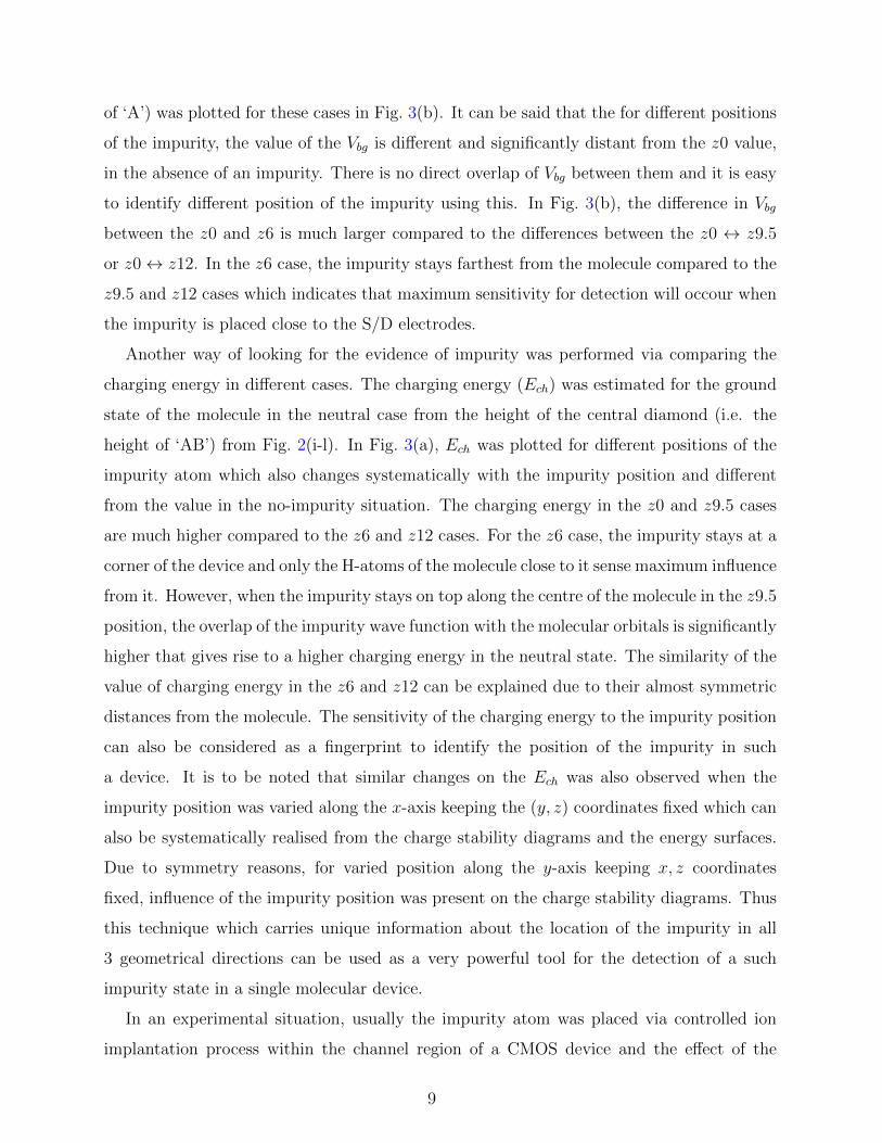
of ‘A’) was plotted for these cases in Fig. 3(b). It can be said that the for different positions
of the impurity, the value of the Vbg is different and significantly distant from the z0 value,
in the absence of an impurity. There is no direct overlap of Vbg between them and it is easy
to identify different position of the impurity using this. In Fig. 3(b), the difference in Vbg
between the z0 and z6 is much larger compared to the differences between the z0 ↔ z9.5
or z0↔ z12. In the z6 case, the impurity stays farthest from the molecule compared to the
z9.5 and z12 cases which indicates that maximum sensitivity for detection will occour when
the impurity is placed close to the S/D electrodes.
Another way of looking for the evidence of impurity was performed via comparing the
charging energy in different cases. The charging energy (Ech) was estimated for the ground
state of the molecule in the neutral case from the height of the central diamond (i.e. the
height of ‘AB’) from Fig. 2(i-l). In Fig. 3(a), Ech was plotted for different positions of the
impurity atom which also changes systematically with the impurity position and different
from the value in the no-impurity situation. The charging energy in the z0 and z9.5 cases
are much higher compared to the z6 and z12 cases. For the z6 case, the impurity stays at a
corner of the device and only the H-atoms of the molecule close to it sense maximum influence
from it. However, when the impurity stays on top along the centre of the molecule in the z9.5
position, the overlap of the impurity wave function with the molecular orbitals is significantly
higher that gives rise to a higher charging energy in the neutral state. The similarity of the
value of charging energy in the z6 and z12 can be explained due to their almost symmetric
distances from the molecule. The sensitivity of the charging energy to the impurity position
can also be considered as a fingerprint to identify the position of the impurity in such
a device. It is to be noted that similar changes on the Ech was also observed when the
impurity position was varied along the x-axis keeping the (y, z) coordinates fixed which can
also be systematically realised from the charge stability diagrams and the energy surfaces.
Due to symmetry reasons, for varied position along the y-axis keeping x, z coordinates
fixed, influence of the impurity position was present on the charge stability diagrams. Thus
this technique which carries unique information about the location of the impurity in all
3 geometrical directions can be used as a very powerful tool for the detection of a such
impurity state in a single molecular device.
In an experimental situation, usually the impurity atom was placed via controlled ion
implantation process within the channel region of a CMOS device and the effect of the
9

impurity can only be observed at low temperature when the thermal excitations are very low.
However, in the present case, the organic molecule based SMT is found to be operational at
300K (room temperature) and the effect of impurity is significantly prominent in all the cases
that can be realised directly from the charge stability diagram, charging energy behaviour
or the dependence of total energy with the gate voltages. Unlike the discrete charge states,
experimentally the charge stability diagram is constructed by using the conductance or the
differential conductance (dI/dV ) on the voltage plane. If the impurity stays in the ’OFF’
region of the device, then its presence can be found as a discrete peak in the I(Vg) scan and
if the impurity is coupled to the two gates as described in the present case, then on a 2D
conduction map on the gate voltage planes, it can be realised in the form of a ‘triple point’
depending of the strength of the impurity-dot coupling.
It is also the noted that in a double gated geometry, the top gate electrode allows ad-
ditional operational control over the electrostatics of the system. On the charge stability
diagram, the central diamond occours in a Vbg range which is different for different cases
and this can be shifted by controlling the Vtg due to almost linear nature of the gate-dot
coupling. This effect was realised by considering the systematic evaluation of the point ‘C’
with Vtg [taken from Fig. 2(f)] and the Vd values estimated from the coordinate of ‘C’ was
plotted as function Vtg in Fig. 3(c). The change of Vd with the change of Vtg is almost linear
under identical electrostatic conditions and this shows that it is possible to find the desired
region of operation by tuning the value of Vtg on the charge stability diagram.
To summarise, in this work the electrostatic behaviour of a double gated SMT was in-
vestigated to understand the influence of an impurity atom using First-principle based cal-
culations in the Coulomb Blockade regime. Due to the extreme sensitivity of the molecular
energy levels to the gate excitation in the weak-coupling limit, the presence of the impurity
atom can be realised from the charge stability diagram which is distinctive for different
positions of the impurity atom. Focussing around a specific region of the charge stability
diagram, it is possible to uniquely identify the signature of the location of the impurity
atom in such devices. The charging energy of the molecule has been found to be sensitive
to the position of the impurity atom that could be used as an identification technique. For
a specific charge state of the molecule, the influence of the impurity atom can also be found
from the energy surfaces (as functions of the gate voltages) which changes with the position
of the impurity atom in the SMT. These together with the charge stability diagram could
10

be used as an electronic fingerprint for the detection of the presence of such impurity atoms
in a nanoscale device. The room temperature operational feasibility of such single molecular
systems allows the possibility of the use of such devices in future molecular electronics as
an alternative to the Si-based single dopant devices where operational feasibility is limited
by low operational temperatures.
[1] Pearson, G. L. and Bardeen, J., Phys. Rev., 75, 5 (1949).
[2] Moraru, Daniel and Udhiarto, Arief and Anwar, Miftahul and Nowak, Roland and Jablonski,
Ryszard and Hamid, Earfan and Tarido, JuliCha and Mizuno, Takeshi and Tabe, Michiharu,
Nanoscale Research Letters, 6, 1 (2011).
[3] Pierre, M. and Wacquez, R. and Jehl, X. and Sanquer, M. and Vinet, M. and Cueto, O.,
Nature Nanotechnology, 5, 1128-1131 (2010).
[4] Shinada, Takahiro and Okamoto, Shintaro and Kobayashi, Takahiro and Ohdomari, Iwao,
Nature, 437, 1128-1131 (2005).
[5] Koenraad, Paul M. and Flatte, Michael E., Nature Nanotechnology, 10, 91-100 (2011).
[6] Hollenberg, L. C. L. and Dzurak, A. S. and Wellard, C. and Hamilton, A. R. and Reilly, D.
J. and Milburn, G. J. and Clark, R. G., Phys. Rev. B, 69, 11 (2004).
[7] Kane, B. E., Nature, 393, 133-137 (1998).
[8] Nonnenmacher, M. and O’Boyle, M. P. and Wickramasinghe, H. K., Applied Physics Letters,
58, 25 (1991).
[9] M. H. Devoret, D. Esteve, and C. Urbina, Nature, 360, 543 (1992).
[10] M. A. Reed, C. Zhou, C. J. Muller, T. P. Burgin, and J. M. Tour, Science, 278, 252 (1997).
[11] J. R. Heath and M. A. Ratner, Physics Today, 43-49 (2003).
[12] Fulton, T. A. and Dolan, G. J., Phys. Rev. Lett., 59, 1 (1987).
[13] Kubatkin, Sergey and Danilov, Andrey and Hjort, Mattias and Cornil, Jerome and Bredas,
Jean-Luc and Stuhr-Hansen, Nicolai and Hedegard, Per and Bjørrnholm, Thomas, Nature,
425, 698-701 (2003).
[14] Osorio, Edgar A. and O’Neill, Kevin and Wegewijs, Maarten and Stuhr-Hansen, Nicolai and
Paaske, Jens and Bjørnholm, Thomas and Van der Zant, Herre S. J, Nano Letters, 7, 11
(2007).
11

[15] Danilov, Andrey and Kubatkin, Sergey and Kafanov, Sergey and Hedegrd, Per and Stuhr-
Hansen, Nicolai and Moth-Poulsen, Kasper and Børnholm, Thomas, Nano Letters, 8, 1 (2008).
[16] K. Stokbro, Journal of Physical Chemistry C, 114, 20461 (2010).
[17] M. Di Ventra, S. T. Pantelides, and N. D. Lang, Phys. Rev. Lett., 84, 979 (2000).
[18] Y.-D. Guo, X.-H. Yan, and Y. Xiao, The Journal of Physical Chemistry C, 116, 21609 (2012).
[19] Ray, S. J. and Chowdhury, R., ArXiv e-prints, 1405.4940 (2014).
[20] Atomistix Tool Kit version 11.2.3, Quantum Wise (http://quantumwise.com/).
[21] K. Kaasbjerg and K. Flensberg, Nano Letters, 8, 3809 (2008).
[22] Park, Hongkun and Park, Jiwoong and Lim, Andrew K. L. and Anderson, Erik H.and
Alivisatos, A. Paul and McEuen, Paul L., Nature, 407, 57-60 (2000).
[23] Liang, Wenjie and Shores, Matthew P. and Bockrath, Marc and Long, Jeffrey R. and Park,
Hongkun, Nature, 417, 725-729 (2002).
[24] Chae, Dong-Hun and Berry, John F. and Jung, Suyong and Cotton, F. Albert and Murillo,
Carlos A. and Yao, Zhen, Nano Letters, 6, 2 (2006).
12