Dielectric Characteristics of Spin-coated Dielectric Films Using ...
11
IEEE Transactions on Dielectrics and Electrical Insulation Vol. 12, No. 6; December 2005 1151 Dielectric Characteristics of Spin-coated Dielectric Films Using On-wafer Parallel-plate Capacitors at Microwave Frequencies A. N. AL-Omari and K. L. Lear Electrical and Computer Engineering Department Colorado State University, Fort Collins, CO 80523-1373, USA ABSTRACT Dielectric properties of spin-coated dielectric insulators suitable for high-speed de- vice fabrication are investigated. Complex dielectric permittivities and tangential ( ) ( ) losses of two polyimides, bisbenzocyclobutene BCB , and a spin-on-glass SOG were extracted from the measured microwave reflection coefficient, S , of 11 parallel-plate capacitors over a frequency range of 50 MHz to 40 GHz. A model for the dielectric permittivity as a function of frequency is developed based on mea- sured data with a minimum square error of less than 10 4 between measured and modeled microwave reflection coefficients. A circuit model for the pad capacitance is obtained based on geometrical and physical considerations. The relationship be- tween the dielectric loss and its thickness is considered. Experimental results are fitted to Debye and Cole-Cole models. Index Terms — Dielectric permittivity, dielectric loss, tangential loss, polymer ( ) ( ) films, polyimide, bisbenzcyclobutene BCB , spin-on glass SOG , Debye model, Cole-Cole model, pad capacitance. 1 INTRODUCTION S devices become smaller, faster and more powerful, A the demands on both materials and processes used by the manufacturers of microelectronic devices become more critical. Dielectrics play a significant role in achiev- w x ing the current state-of-the art in microelectronics 1-3 . They are typically applied in semiconductor micro-fabri- cation for a number of applications such as stress buffers to accommodate built-in strains as well as strain induced w x by forced bending 4, 5 , surface planarization and passi- wx w x wx vation 6 , dielectric isolation layers 7,8 , die bonding 9 , w x and buried channel waveguides 10 . Spin-on dielectrics are used in fabricating many high speed electronic devices for reduction of parasitic circuit elements that may limit device speed. In heterojunction Ž . bipolar transistors HBTs , parasitics were reduced by col- w x lector implantation 11 or by double polymer planariza- w x tion 12 . A multilayer polymer structure was used to re- duce parasitic capacitance of permeable base transistors Ž . w x PBTs, i.e. vertical MESFETs 13 . In vertical-cavity sur- Ž . face emitting lasers VCSELs , polymer was used for pla- narization, passivation and metal pad parasitic capaci- w x Ž . tance reduction 14 . Spin-on glass SOG has been ac- Manuscript recei®ed on 6 July 2004, in final form 14 April 2005. w x tively investigated 15-17 for similar applications and has w been used in multilevel metal interconnect processes 15, x 16 . When a dielectric material is subjected to an electric field, the bound positive and negative charge constituents are displaced from their average equilibrium positions by the Lorentz electric field forces. The charge adjustment results in several polarization mechanisms including dipo- lar polarization, ionic polarization, and electronic polar- w x ization 18 . Dipolar or orientational polarization occurs when permanent dipoles in asymmetric molecules re- spond to the applied electric field. Ionic polarization arises when adjacent positive and negative ions are displaced in the presence of an applied electric field. Electronic polar- ization occurs in neutral atoms when an electric field dis- places the negative electron cloud with respect to the pos- itive nucleus. Each polarization mechanism has an associ- ated response time and therefore will not contribute to the dielectric constant beyond some corresponding fre- w x quency 19 . The maximum effective response frequency of dipolar, ionic, and electronic mechanisms are on the 10 12 15 w x order of 10 Hz, 10 Hz and 10 Hz, respectively 19 . In this work, dielectric properties of four different spin- Ž . on dielectrics Table 1 which are typical options for pla- narization in the applications mentioned above are inves- 1070-9878 r 05 r $20.00 2005 IEEE
-
Upload
khangminh22 -
Category
Documents
-
view
0 -
download
0
Transcript of Dielectric Characteristics of Spin-coated Dielectric Films Using ...
IEEE Transactions on Dielectrics and Electrical Insulation Vol. 12, No. 6; December 2005 1151
Dielectric Characteristics of Spin-coated Dielectric FilmsUsing On-wafer Parallel-plate Capacitors at Microwave
FrequenciesA. N. AL-Omari and K. L. Lear
Electrical and Computer Engineering DepartmentColorado State University, Fort Collins, CO 80523-1373, USA
ABSTRACTDielectric properties of spin-coated dielectric insulators suitable for high-speed de-vice fabrication are investigated. Complex dielectric permittivities and tangential
( ) ( )losses of two polyimides, bisbenzocyclobutene BCB , and a spin-on-glass SOGwere extracted from the measured microwave reflection coefficient, S , of11parallel-plate capacitors over a frequency range of 50 MHz to 40 GHz. A model forthe dielectric permittivity as a function of frequency is developed based on mea-sured data with a minimum square error of less than 10�4 between measured andmodeled microwave reflection coefficients. A circuit model for the pad capacitanceis obtained based on geometrical and physical considerations. The relationship be-tween the dielectric loss and its thickness is considered. Experimental results arefitted to Debye and Cole-Cole models.
Index Terms — Dielectric permittivity, dielectric loss, tangential loss, polymer( ) ( )films, polyimide, bisbenzcyclobutene BCB , spin-on glass SOG , Debye model,
Cole-Cole model, pad capacitance.
1 INTRODUCTIONS devices become smaller, faster and more powerful,A the demands on both materials and processes used
by the manufacturers of microelectronic devices becomemore critical. Dielectrics play a significant role in achiev-
w xing the current state-of-the art in microelectronics 1-3 .They are typically applied in semiconductor micro-fabri-cation for a number of applications such as stress buffersto accommodate built-in strains as well as strain induced
w xby forced bending 4, 5 , surface planarization and passi-w x w x w xvation 6 , dielectric isolation layers 7,8 , die bonding 9 ,
w xand buried channel waveguides 10 .
Spin-on dielectrics are used in fabricating many highspeed electronic devices for reduction of parasitic circuitelements that may limit device speed. In heterojunction
Ž .bipolar transistors HBTs , parasitics were reduced by col-w xlector implantation 11 or by double polymer planariza-
w xtion 12 . A multilayer polymer structure was used to re-duce parasitic capacitance of permeable base transistorsŽ . w xPBTs, i.e. vertical MESFETs 13 . In vertical-cavity sur-
Ž .face emitting lasers VCSELs , polymer was used for pla-narization, passivation and metal pad parasitic capaci-
w x Ž .tance reduction 14 . Spin-on glass SOG has been ac-
Manuscript recei®ed on 6 July 2004, in final form 14 April 2005.
w xtively investigated 15-17 for similar applications and haswbeen used in multilevel metal interconnect processes 15,
x16 .
When a dielectric material is subjected to an electricfield, the bound positive and negative charge constituentsare displaced from their average equilibrium positions bythe Lorentz electric field forces. The charge adjustmentresults in several polarization mechanisms including dipo-lar polarization, ionic polarization, and electronic polar-
w xization 18 . Dipolar or orientational polarization occurswhen permanent dipoles in asymmetric molecules re-spond to the applied electric field. Ionic polarization ariseswhen adjacent positive and negative ions are displaced inthe presence of an applied electric field. Electronic polar-ization occurs in neutral atoms when an electric field dis-places the negative electron cloud with respect to the pos-itive nucleus. Each polarization mechanism has an associ-ated response time and therefore will not contribute tothe dielectric constant beyond some corresponding fre-
w xquency 19 . The maximum effective response frequencyof dipolar, ionic, and electronic mechanisms are on the
10 12 15 w xorder of 10 Hz, 10 Hz and 10 Hz, respectively 19 .
In this work, dielectric properties of four different spin-Ž .on dielectrics Table 1 which are typical options for pla-
narization in the applications mentioned above are inves-
1070-9878rrrrr05rrrrr$20.00 � 2005 IEEE

AL-Omari and Lear: Dielectric Characteristics of Spin-coated Dielectric Films1152
Table 1. Families, specific verities and general properties of the investigated dielectrics.
Specific variety HD-8000 PI-2723 BCB-4024 SOG IC1-200TM TM TMManufacturer HD Microsystems HD Microsystems Dow Chemical Cyclotene Futurrex, Inc.
Dielectric material Organic polymer Organic polymer Organic polymer Spin On GlassFamily Polyimide Polyimide Bisbenzo- cyclobutene PolysiloxaneTone positive negative negative non-photosensitive
aŽ .Cured film thickness �m 5�11 1.8�8.5 3.5�7.5 0.5b Ž .Tg �C 300 �320 �350 �
c Ž Ž .CTE ppmr �C 47 57 52 �Ž .Elongation % 11 12 8 �
4 6 6Ž .Breakdown field Vrcm � �2�10 3�10 3�1016 19 13Ž .Volume resistivity �-cm � �10 10 5�10
Ž .Tensile modulus Gpa 2.5 2.7 2.9 �Ž .Tensile strength Mpa 122 160 87 20
a: Achieved by double spin coating.b: Glass Transition Temperature.c: Coefficient of Thermal Expansion.
tigated using the capacitance of high speed VCSEL metalpads as a test geometry for the samples. The developmentof an accurate equivalent circuit for VCSELs as well asother devices motivates the measurement of complex di-electric permittivities and tangential losses for polyimide,bisbenzocyclobutene, and spin-on-glass dielectrics up to40GHz. The resulting circuit models are useful for theanalysis of bandwidth limitations of laser diodes and otherhigh speed electronic devices as well as matching drivercircuits to device impedances.
2 FABRICATIONIn high speed VCSEL fabrication, dielectrics are used
to planarize etched mesas before depositing metal inter-w xconnects and bonding pads 14 . A smooth surface is
needed for metal interconnect and metal bonding padlithography and deposition. Polymer coatings also protectthe sidewalls of the mesa from the external environment,and it creates an isolation layer between n and p con-tacts. Although the thermal conductivity of most polymersis poor, it is better than the thermal conductivity of gasesin hermetic packages or air. The dielectric properties ofthe materials used in this work were investigated by fabri-cating capacitors from the different dielectric materialswith various thicknesses and measuring their microwave
Ž .scattering parameters S-parameters .
2.1 FABRICATION OVERVIEWCapacitors corresponding to the probe pads of VCSELs
were fabricated above conducting ground planes on un-doped GaAs substrates as illustrated in Figure 1 whichshows a cross-section along AA’ of Figure 2. The geome-try shown in Figure 2 is nominally that of parallel plateswith constant dielectric thickness. While some fringingfields exist, the 80 �m width of the central metal pad ismuch larger than the 0.7 to 7.0 �m dielectric thicknesslisted in Table 2, and there is a relative large minimumseparation of 10 �m between the central signal and theoutside ground pads. Thus the fringing field effects have
Figure 1. Capacitor cross-section at AA’ in Figure 2.
Figure 2. SEM photo for a completed capacitor ready for testing.
been neglected in this study. While a simpler or a largerpad geometry might reduce fringing fields, the triple padconfiguration was required for compatibility with coplanarmicrowave probes, and the annular aperture region waspresent in the features of the VCSEL photo mask. To formthe ground plane, which serves as the lower plate of thecapacitor, layers of Ti-Au-Ti with thicknesses ofŽ .100r170r100 nm were evaporated in sequence on top ofthe substrate. In addition to serving as the capacitor’s bot-tom plate, these ground plane layers shield the capacitors
IEEE Transactions on Dielectrics and Electrical Insulation Vol. 12, No. 6; December 2005 1153
Table 2. Dielectrics fabrication process summary.Specific Sample Spin speed Developing Cured
3Ž . Ž . Ž .variety number �10 rpm time s thickness �m
HD-8000 1 10.0 40 1.362 5.0 55 3.63 3.5 80 5.5
PI-2723 4 5.5 25 1.355 2.0 30 4.16 1.3 46 6.0
BCB-4024 7 7.5 20 1.88 3.5 30 4.39 2.5 55 7.2
IC1-200 10 3.0 � 0.65
from the properties of the substrate. The lower layer of Tiwas applied to improve the adhesion of the Au layer tothe substrate while the upper Ti layer improves the adhe-sion of the spin-on dielectric to the lower metal. Au andTi layers were chosen to be thick enough to withstand thedielectric surface tension and contraction during the cur-ing process. Next, each one of the four different types ofdielectrics listed in Table 1 were spun on the ground planeand appropriately patterned and cured. Details of the di-electric fabrication processes will be discussed individuallyin Section 2.2. Table 1 also shows the general family ofthe dielectric materials along with their tones, manufac-turers, and specific part numbers.
The capacitor’s top plate was fabricated with a metalpad mask suitable for on-wafer microwave testing. Theco-planar pad configuration was originally designed for usein fabricating VCSELs including an annular contact re-gion as seen in Figure 2. In the present work, the entirepad and annular contact region are insulated from theground plane by a constant thickness dielectric layer. Thepad design greatly reduces inaccuracies in microwaveprobing associated with parasitic coupling and unwanted
w xmode excitation at the probing tips 20 . A ground-signal-Ž .ground GSG contact configuration was chosen as it ter-
minates field lines at the interface effectively and excitesthe unwanted microstrip modes less than other contact
w xconfigurations 20, 21 .
The metal probe pads and thus capacitor top plates werepatterned using the same lift-off process on ten dielectric
Žsamples of varying thicknesses of the four materials Ta-.ble 2 . The photolithography step used AZ4400 photore-
sist that was soaked in chlorobenzene for five minutesprior to developing to obtain a suitable profile for the lift-
w xoff process 22 . Next, the samples were developed usingŽ .AZ400K developer diluted with DI water 1:4 . To reduce
the resistance between the ground pads of the top plateand the lower Ti-Au-Ti ground plane, the titanium oxidelayer TiO that formed on the exposed ground plane dur-2
ing the curing process was wet etched in hydrofluoric acidŽ . Ž .HF diluted with DI water 5% : 95% for � 5 s which islong enough to remove the TiO layer and short enough2
to maintain the dielectric’s surface smoothness. Then, Ti-Ž .Au was evaporated with thicknesses of 30r300 nm re-
w xspectively 22 . Figure 2 shows an SEM photo of a com-pleted capacitor structure using the high-speed VCSELmetal interconnect pad design.
2.2 DIELECTRICS FABRICATION(2.2.1 POLYIMIDES HD-8000 AND)PI2723
Polyimides have been identified as having excellent po-tential for use in high speed electronic devices, aerospacecomposites, and air craft wire and cable coating amongother applications due to their high inherent thermal sta-bility, and excellent electrical and mechanical propertiesw x23 . One potential disadvantage of polyimides is their
w xmoisture absorption 24 . Polyimides are cyclic-chainpolymers which are mainly synthesized by a two-step tech-nique. First, polyamic acid is formed by a condensationreaction of a tetracarboxylic acid dianhyride with a dys-
Ž .functional base diamine . Polyamic acid is readily solublein polar organic solvents. In the second step of the synthe-sis polyamic acid is cyclodehydrated to the correspondingpolyimide by extended heating at an elevated temperaturew x w x25 , by treating with chemical dehydrating agents 26 , or
w xby microwave energy 27 . A typical molecular structurefor a photosensitive polyimide after curing is shown in
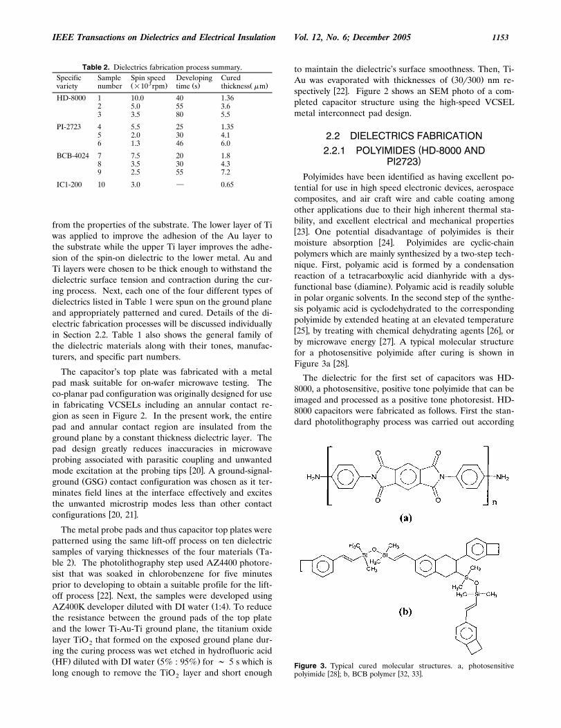
w xFigure 3a 28 .
The dielectric for the first set of capacitors was HD-8000, a photosensitive, positive tone polyimide that can beimaged and processed as a positive tone photoresist. HD-8000 capacitors were fabricated as follows. First the stan-dard photolithography process was carried out according
Figure 3. Typical cured molecular structures. a, photosensitivew x w xpolyimide 28 ; b, BCB polymer 32, 33 .
AL-Omari and Lear: Dielectric Characteristics of Spin-coated Dielectric Films1154
to the manufacturer’s data sheet. To obtain different di-electric thicknesses, different spinning speeds were usedfor this type of polyimide as well as all other types of di-electrics used in this study. After exposure, the samplewas baked for 100s at 115�C. Then, it was left to cool downto ambient temperature for about 30 minutes prior to pro-ceeding with the developing step. Developing polyimidewhile it is hot leads to severe cracks in the cured poly-imide as shown in the inset of Figure 2. Dipping a hotsample in the developer will drop the cured polyimidesurface temperature to 20�C while the temperature of thepolyimide underneath the surface is about 120�C. As aresult the surface of the polyimide contracts more thanthe polyimide underneath, with the resulting stress crack-ing the polyimide. The polyimide was developed in thecommonly used AZ400K aqueous developer diluted with
Ž . Ž .deionized DI water 1:4 . After developing, the samplewas rinsed by squirting it with DI water while it was spun
Ž .at 1000 revolution per minute rpm for 10 s. Immediatelyafter the rinse, it was spin-dried at 3500 rpm for 10 s. Tocure the polyimide the sample was loaded into a curingfurnace at 20�C in a nitrogen atmosphere, and the tem-perature was ramped from 20 to 350�C over a 60 minuteperiod. The temperature was held at 350�C for 30 min-utes. Finally, the sample was allowed to cool down. Thespinning speeds, developing times, and measured HD-8000polyimide thicknesses after curing are listed in Table 2.
Pyralin� PI-2723 polyimide is a photosensitive negativetone organic polymer which was used to fabricate the sec-ond set of capacitors. After the photolithographic expo-sure, the polyimide was developed using DE-6018 solvent,then further developed in DE-6018 diluted with RI-9045
Ž .solvent 1:1 , and finally rinsed using RI-9045. To cure thepolyimide, the sample was loaded into furnace at 20�C,and the temperature was ramped from 20 to 150�C atabout 6.5�Crminute. Then the temperature was rampedfrom 150 to 300�C over a 60 minute period. The tempera-ture was held at 300�C for 30 minutes. Table 2 lists thecured thicknesses of the PI-2723 polyimide as well as otherprocess parameters.
2.2.2 BISBENZOCYCLOBUTENE( )BCB-4024Ž .Bisbenzocyclobutene BCB has been traditionally used
Ž .as a polymer dielectric for many multichip module MCMw x TMapplications 29 . The thermal curing of Cyclotene
polymers is a two-step process. First the benzocyclobutenering opens thermally to produce an o-quinodimethane in-termediate. Next, the o-quinodimethane undergoes aDiels-Alder reaction with residual alkene groups in theprepolymer, forming a tri-substituted tetrahydronaphtha-
w xlene 30 . One difference with respect to polyimide is thatBCB does not evolve water during crosslinking. After cur-ing, the crosslinked BCB polymer has low moisture up-take. The main disadvantage of BCB is the thermal stabil-
w xity of the cured film 31 . Figure 3b shows standard curedw xphotosensitive BCB polymer structure 32, 33 .
BCB-4024 is a photosensitive, negative-tone polymerthat was used for the third set of capacitors. Following thephotolithographic exposure process, the polymer was de-veloped using the DS-2100 solvent. To cure the polymerthe sample was loaded into a furnace and the tempera-ture was ramped from 20 to 150�C at 4.5�Crminute. Thetemperature was held at 150�C for 15 minutes. Then, thetemperature was ramped from 150 to 250�C over a 10minute period. The temperature was held at 250�C for 40minutes. The measured BCB-4024 polymer thicknesses af-ter curing are shown in Table 2 along with the corre-sponding developing times and spinning speeds.
( )2.2.3 SPIN-ON GLASS IC1-200Intermediate coating IC1-200 is a high transparency
polysiloxane-based spin-on dielectric material, which con-tains methyl and unspecified alkoxy groups bounded tosilicon atoms with carbon contents in the range of 20-30%w x34 . IC1-200 is used primarily in the planarization of to-pography on integrated circuits in multilevel metal tech-niques. SOG is applied as a dielectric in a permanent or apartial etchback mode. It can be utilized as an intermedi-ate layer in the trilayer resist technique and as a protec-
w xtive layer for plastics and metals 34 .
IC1-200 was spun at 3000 rpm for 30 s. Then it wasbaked on a hot plate at 100�C for one minute and at 200�Cfor another one minute. Next, a second layer of SOG wasspun and baked at same temperatures used for the firstlayer. After that, positive tone photoresist was patternedand developed to serve as a mask covering a part of theSOG area. The exposed SOG was etched using an reac-
Ž .tive ion etching RIE system for ten minutes with chlo-Ž .rine and oxygen 2:1 at approximately 100mW power and
Ž .20 Pa 150 mTorr pressure. Then the photoresist wasstriped and the SOG was cured at 400�C for 30 minutes ina nitrogen gas flow that prevents the SOG from oxidation,which can cause flakes to form. After curing the SOG hasan approximate thickness of �0.65 �m. Only this singlethickness was used to fabricate SOG capacitors. The ven-dor recommended a maximum film thickness of �0.5 �mas thicker films can have excessive tensile stress that leadsto the film cracking. Table 2 summarizes the cured dielec-tric thicknesses and their corresponding developing timesand spinning speeds.
3 MEASUREMENTSThe fundamental properties of dielectric materials can
be measured either in the frequency domain or in the timedomain using suitable transformation techniques to obtainthe frequency dependence of the materials properties. Onemotivation for the development of time domain tech-niques was the necessity of different frequency domain

IEEE Transactions on Dielectrics and Electrical Insulation Vol. 12, No. 6; December 2005 1155
methods and instruments to cover a frequency range of 1w xHz up to 10 GHz 35 . Frequency domain measurements
were used in this study since time-domain techniques as-sume the system is linear and any unexpected non-linear-ity introduces complications in the transformation tech-
w xnique to be adapted 35, 36 . Furthermore it is now possi-ble to use a single instrument to cover a wide range offrequencies.
A variety of techniques can be used to measure theproperties of dielectric materials in the frequency domain.The auto balancing bridge technique is accurate in thefrequency range from a few Hz to 110MHz. The current-
Ž .voltage IV and RF-IV techniques are also accurate andcan be applied from 40 Hz to 3 G Hz. TheTransmissionrReflection technique can be utilized for a
w xfrequency range from a few Hz to 110GHz 37 .
Based on the frequency range of the available equip-ment, the transmissionrreflection technique was applied.The S parameter measurement apparatus consisted of11
Ž .an Agilent 8722ET vector network analyzer VNA with40 GHz bandwidth, a computer with GPIB card to loadthe calibration kit into the VNA, a high precision Cascade
Ž .Microtech impedance standard substrate ISS-101-190 , aprobe station with a room temperature stage, a fiber opticilluminator to reduce sample temperature variations, aCCD camera, and Cascade Microtech air co-planar probesŽ .ACP40 with a GSG configuration, 125 �m pitch, andBe-Cu tips which provide repeatable contact on gold pads.The use of ACP with GSG configuration helps deliver theRF signals with minimal attenuation and good impedance
w xcontrol, which results in accurate measurements 38 .
The S parameter measurements proceeded as follows;11
isopropyl alcohol diluted with DI water and lint-free wipeswere used to clean the mating surfaces so that the mea-surements are not affected by dirt and impurities. RF ca-ble reflection stability and connector repeatability wereverified. The largest drift in the reflection coefficient forthe cable terminated with an open circuit was y57 dBwhich corresponds to a 0.0014 change in voltage ampli-
Figure 4. Real part of S parameter vs. frequency.11
Figure 5. Imaginary part of S parameter vs. frequency.11
tude. The VNA was calibrated at a power level of y10Ž .dBm 0.1 mW in order to maximize signal to noise ratio
while not being so large as to require attenuation of thereflected signal. A low IF bandwidth of 100Hz was used toreduce noise. The measurement repeatability was im-proved by operating the VNA in stepped frequency mode,rather than with continuous sweep and by applying theVNA built in averaging and smoothing functions. One-port
Ž .calibration using a standard short-open-load SOL wascarried out. Next the capacitor’s microwave reflection co-efficients were measured over a frequency range of 50MHz to 40 GHz. Figures 4 and 5 show the real and imagi-nary parts of the measured reflection coefficients respec-tively for the dielectrics listed in Table 1. The raw dataexhibited some ripples with magnitudes on the order of10y3 that were filtered out using the VNA built-insmoothing and averaging functions. To maintain clarity,only the data for selected dielectric thicknesses are shown.
4 COMPLEX PERMITTIVITY ANDTANGENTIAL LOSS EXTRACTION
The complex permittivity and tangential loss are re-garded as the most important parameters for describing
w xdielectric properties 39 . The relative permittivity can beexpressed in the complex form ��s � �
� j��, where � � isthe relative dielectric constant which characterizes a ma-terial’s ability to store charges, and �� is the dielectricloss which is a measure of the dissipation in the material.The dielectric loss is typically quantified in terms of a ma-terial’s dielectric loss tangent, tan �� �s��r� �, where �d d
w xis the dielectric loss angle 40, 41 .
The impedance of a capacitor with a lossy dielectric isŽ � . w xgiven by Z s dr j�� � A 42 , where � is the free0 0
space permittivity 8.85 x 10 �12 Frm, A is the capacitorarea which is fixed for all capacitors in this study at 10400�m2, d is the thickness of the dielectric, and � is theangular frequency. The measured impedances of the fab-ricated capacitors can be calculated from the measured

AL-Omari and Lear: Dielectric Characteristics of Spin-coated Dielectric Films1156
Figure 6. Measured real part of dielectric permittivity vs. fre-quency.
Ž . Ž .reflection coefficients by ZsZ 1qS r 1� S ,0 11meas 11meas
where S is the measured reflection coefficient and11measŽ .Z is the vector network analyzer impedance 50� . Theo
relation between the measured and calculated capacitors’w ximpedances is expressed as 42
d 1qS11m eassZ 1Ž .0 ž /j�� � ’� j� ’’ A 1� SŽ .0 11m eas
Ž .Solving equation 1 for the real and imaginary parts of� �
� j�� results in
d 1 1� S11meas�� � s Im 2Ž . Ž .ž / ž /�� A Z 1qS0 0 11meas
d 1 1� S11meas�� � s Re 3Ž . Ž .ž / ž /�� A Z 1qS0 0 11meas
�Ž . �Ž .Figures 6 and 7 illustrate � � and � � extractedŽ . Ž .from the measured data using equations 2 and 3 re-
spectively. The tangential loss, tan � � �, is shown in Fig-d
ure 8 and was obtained by calculating the ratio�Ž . �Ž . w x Ž . Ž .� � r� � 41 using results from equations 2 and 3 .
The data clearly show the frequency dependence of� �,��, and tan � � � for the studied dielectrics. The reald
part of the dielectric permittivity for all studied dielectricsmonotonically decreases as frequency increases. The di-electric losses and thus loss tangents initially increase ap-proximately linearly in frequency before reaching a broadpeak and then decreasing. Such a response corresponds
wto the presence of one or more relaxation phenomena 36,x41, 43 . The maximum dielectric loss for HD-8000, PI-
2723, BCB-4024 and IC1-200 occurs at frequencies of 30,33, 32, and 25 GHz, respectively.
The dielectric parameters � �, ��, and tan � � � vary ind
frequency as the different polarization mechanisms dis-
Figure 7. Measured dielectric loss vs. frequency.
Figure 8. Measured dielectric tangential loss vs. frequency.
w xcussed in the introduction are selectively excited 18, 19 .As the frequency of the applied field is increased, a point
Žis reached where the permanent electric dipoles polar.molecules of the material can no longer rotate fast enough
to remain in phase with the field. Therefore, contributionsof the dipolar polarization mechanism to the net polariza-tion declines, which subsequently causes a reduction in � �,��, and tan � � �.d
5 MODELING AND DATA FITTINGCircuit models are useful for the analysis of high speed
bandwidth limitations of electronic devices as well asmatching driver circuits to device impedances. A circuitmodel for the capacitors was developed based on geomet-rical and physical considerations. The circuit model, shownin the inset of Figure 8, consists of elements correspond-ing to the physical features of the capacitor, where Cp
denotes a lossless capacitor between the metal intercon-nect Ti-Au on top of the dielectric and the bottom plateTi-Au-Ti. The fringing field at the sides of the top plate

IEEE Transactions on Dielectrics and Electrical Insulation Vol. 12, No. 6; December 2005 1157
was neglected since the associated fringing capacitancew xwas estimated to be less than 3fF 44 . A resistor, R , inloss
series with the capacitor models the loss associated withthe dielectric dissipation and the shunt resistor, R ,shunt
represents the resistance of the dielectric material at DCor low frequency due to the leakage current in the capaci-tor. R is usually on the order of multi-gigaohms andshunt
was assumed to be so large that it has a negligible effecton the model. Numerical calculations assumed a value ofR s 1012 � to improve convergence. The resistanceshunt
in the leads and plates of the capacitor is relatively small.The dc plate resistance was estimated to be � 0.15 �.
w xAccording to classical theory 45 , the ac surface resis-Ž . Ž .1r2tance of a conductor is R � s � �r2 , where s 0
is the electrical conductivity which equals 4.1 x 10⁷ � �1m�1
and 2.3 x 10⁶ � �1m�1 for Au and Ti respectively, and �0
is the material permeability that is 4 x 10 � 7 Hrm fornon-ferromagnets. The maximum surface resistance val-ues for Au and Ti at 40 GHz were approximately 0.06
Ž .and 0.26 �, respectively. The skin depth is given by � �sŽ .1r2 �s 2r�� for a good conductor assuming r�� �10
w x46-49 . At 40 GHz, the skin depths of Au and Ti wereestimated to be 2.1 �m and 0.39 �m respectively whichare larger than the capacitor’s plate thickness of 0.33 �m.Therefore the capacitor plates dc resistance, ac resistance,and skin effect were neglected in the present model andsubsequent analysis.
The circuit model impedance can be calculated as
1 dZ sR q s 4Ž .� �model loss j�C j�� � � j� AŽ .p 0
Ž .Solving equation 4 for C results inp
��2 � � �A0C s 1� � 5Ž .p � 2 ž /ž / d�
�2 � 2 Ž .Since � r� �1, equation 5 can be reduced to Cp s� � �Ard so the frequency dependence of the capacitance0
Figure 9. Capacitance vs. frequency.
is nearly proportional to the frequency dependence of � �.Ž .Solving equation 4 for R results inloss
�� ��2 dR s 1� � 6Ž .loss � 2 � 2 ž /ž / �� A� � 0
Ž � �2 .Ž .which can be approximated as R s � r� dr�� Aloss 0
by again neglecting ��2r� �2.
The functional dependence of � � and R on fre-loss
quency were found to be well approximated by a Gaussianfunction with fitting parameters adjusted to minimize thesquare error to less than 10 � 4. Figures 9 and 10 illustratethe extracted and fitted data for C and R respec-p loss
tively, for the four dielectric materials investigated. TheGaussian functions and coefficients that result in the bestfit are listed in Table 3. The values of the real dielectric
Ž . Žpermittivity at dc f s 0 and very high frequencies f™.� were found to be in reasonable agreement with the
predicted ones from the Cole-Cole model as discussed inthe next section. Furthermore, values of the real dielectricpermittivity at f s 0 were found to be in reasonableagreement with the low-frequency dielectric permittivityvalues provided by the material vendors and reported by
w xothers 34, 50 which are also listed in Table 3. As seen inFigure 10, the extracted values for R are moderatelyloss
constant across the frequency range studied, justifying theseries resistance model. Average values of R are listedloss
in the table as well, and these constant resistances maysuffice in simplified circuit models. The 95% confidencelimits for the values of � , � , f , R and f are listedLF � o LF 1
in Table 4.
To further investigate the properties of the dielectricsunder test, capacitors were fabricated using three differ-ent thicknesses of each of the three organic polymers. S11
parameters were measured and fitted to the circuit modelas discussed earlier for each thickness. Figure 11 illus-trates R as a function of the polymer thickness. Resultsloss
show a linear, approximately proportional dependence on
Figure 10. Dielectric loss equivalent resistance vs. frequency.
AL-Omari and Lear: Dielectric Characteristics of Spin-coated Dielectric Films1158
�Ž . Ž .Table 3. � f and R f Gaussian functions with their best fitting parameters � , � , f , R and f .loss LF � o L F 12 2f f
� . .yŽ yŽŽ . Ž . Ž .2 2Specific � Thickness � f s � y� �e q� R R f sR �ef fL F L F � � loss loss L Fo 1
Ž . Ž . Ž . Ž .variety § � ‡ �m � � f GHz C f � R fL F � o p L F 1
HD-8000 3.4 3.9 � 3.6 3.9 2.7 103 10 10.7 75�PI-2723 3.3 4.3 � 4.1 4.3 3.1 120 11 12.3 80Ž .� � f Aow50xBCB-4024 3.3 3.5 2.6 4.3 3.5 2.4 110 11 10.2 80
w34x dIC1-200 2.65 2.35 2.3 0.65 2.4 1.2 70 2.8 3 80
§: vender � : extracted from Figure 13.�Ž .�: present work f and f : fitting parameters GHz .o 1
‡: others C : pad capacitance.p� : dielectric constant at low frequency. R : resistance associated with the dielectric loss at low frequency.LF LF
Ž .f : operating frequency GHz .
Table 4. � � and R Gaussian functions best fitting parameters � , � , f , R , f , and , and their 95% confidence limits.loss L F � o L F 1
HD-8000 PI-2723 BCB-4024 IC1-200
� 3.9q0.10ry0.14 4.3q0.07ry0.12 3.50.06 2.4q0.06ry0.05LF� 2.7q0.05ry0.06 3.1q0.05ry0.09 2.4q0.03ry0.04 1.2q0.07r0.05�Ž .f GHz 103q3ry13 120q7ry14 110q7ry6 70q5ry4o
Ž .R � 10.70.4 12.3q0.3ry0.2 10.2q0.1ry0.2 30.1L FŽ .f GHz 75q5ry3 805 80q4ry2 80q5ry61
0.1q0.05ry0.04 0.11q0.6ry0.5 0.22q0.04ry0.1 0.48q0.1ry0.7
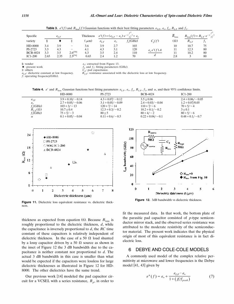
Figure 11. Dielectric loss equivalent resistance vs. dielectric thick-ness.
Ž .thickness as expected from equation 6 . Because R isloss
roughly proportional to the dielectric thickness, d, whilethe capacitance is inversely proportional to d, the RC timeconstant of these capacitors is relatively independent ofdielectric thickness. In the case of a 50 � load shuntedby a lossy capacitor driven by a 50 � source as shown inthe inset of Figure 12 the 3 dB bandwidth due to the ca-pacitance is neither constant nor proportional to d. Theactual 3 dB bandwidth in this case is smaller than whatwould be expected if the capacitors were lossless for largedielectric thicknesses as illustrated in Figure 12 for HD-8000. The other dielectrics have the same trend.
w xOur previous work 14 modeled the pad capacitor cir-cuit for a VCSEL with a series resistance, R , in order top
Figure 12. 3dB bandwidth vs dielectric thickness.
fit the measured data. In that work, the bottom plate ofthe parasitic pad capacitor consisted of p-type semicon-ductor mirror stack, and the observed series resistance wasattributed to the moderate resistivity of the semiconduc-tor material. The present work indicates that the physicalorigin of most of this equivalent resistance is in fact di-electric loss.
6 DEBYE AND COLE-COLE MODELSA commonly used model of the complex relative per-
mittivity at microwave and lower frequencies is the Debyew xmodel 41, 43 given by
� � �LF ��� f s� q 7Ž . Ž .� 1q jfrfŽ .peak

IEEE Transactions on Dielectrics and Electrical Insulation Vol. 12, No. 6; December 2005 1159
where f is the frequency, f is the relaxation frequencypeak
at which the dielectric loss peaks, � is the dielectricLF
constant at low frequency, and � is the dielectric con-�
stant at f � f . A key advantage of the Debye model ispeal
that its inverse Fourier transform is an exponential func-tion which permitted the development of numerous com-putationally effective algorithms to incorporate Debyematerials into finite difference time domain simulationsŽ . w xFDTD 43, 49 . Conversely, the Debye model is often apoor predictor of the dielectric performance of most phys-ical materials since the original Debye treatment for polarmolecules assumes that the molecules are spherical inshape and as a result the axis of rotation has no effect on
�Ž .the value of � f . Furthermore, it neglects the interac-w xtions between the molecules in the dielectric material 43
w xthat in practicality are not negligible 51 . Accordingly, theDebye model incorporates only one relaxation frequency
w xf 49 .peak
More accurate models account for molecular interac-w x w xtions 52, 53 and for asymmetric molecular shapes 52 .
An example of such an improved model is that of Cole-w xCole 43, 54 ,
� � �LF ��� f s� q 8Ž . Ž .� 1 � a1q jfrfŽ .peak
where is an experimental fitting parameter in the range0F F1. The Debye model is a special case of the Cole-Cole model when s0. It should be noted that theCole-Cole model’s non-integer value of hinders its in-
w xclusion in FDTD computations 49 .
To investigate the applicability of the two models men-tioned above, approximate values of � for all four di-�
Ž �electrics were estimated utilizing the Cole-Cole plot �� .on the x-axis and � on the y-axis by extrapolating the
Ž .values of � to f™� using equation 8 . A best fit for eachdielectric material was achieved by allowing the values for� , � , and to vary. The best fit values and the 95%LF �
confidence limits for � , � , and are listed in Table 4.LF �
Ž .By applying values of � and � in equation 7 plots forLF �
the Debye model were also obtained. Figure 13 below il-lustrates the Cole-Cole plots obtained from experimentalmeasurements, the Debye model, and the Cole-Colemodel. The measured curves are very close to a circular
w xarc in conformity with the Cole-Cole model 52, 54 .
Based on the plots presented in Figure 13 it is con-cluded that there are considerable inter-molecular inter-
w xactions in organic polymers and SOG 53, 54 . Further-w xmore, the results presented here support the claim in 53
which states that the simple Debye model cannot ade-quately describe the relaxation process in these materials.However, the Cole-Cole model well describes the experi-mental data.
Most materials require a finite time for polarization tooccur. This time dependence results in a relaxation time �that is defined as the time interval characterizing the
Figure 13. Cole-Cole complex plane plots obtained from experi-mental measurements, Debye model and Cole-Cole model.
restoration of distributed molecules to their equilibriumstate under the effect of an electric field. For dielectrics
Žwhich cannot be described by the Debye model one re-.laxation time , several analytical relations that give a rela-
tively good agreement with the experimental data re-ported here have been proposed to describe the relax-
Ž . w xation time distribution function G � 35, 36, 54, 55 .
7 CONCLUSIONSIn this paper, on-wafer, parallel-plate capacitors were
fabricated from four different spin-on dielectrics. Multi-ple dielectric thicknesses were used for the three organicdielectrics. Microwave reflection coefficients, S , were11
measured up to 40 GHZ Dielectric permittivities andlosses as a function of frequency were extracted frommeasured microwave reflection coefficients, S , of the ca-11
pacitors. The dielectric permittivity is well approximatedby a gaussian function, while the dielectric loss and tan-gential loss peak in the 25 to 34 GHz range. A simplecircuit model for the fabricated capacitor was obtainedwith a minimum square error of less than 10-4 betweenmeasured and modeled reflection coefficients. The behav-ior of the capacitors over frequency is well approximatedby a lossless capacitor with a frequency dependent dielec-tric permittivity and a constant series resistance. Measure-ments of different organic polymer dielectric thicknessesconfirm that the equivalent series resistance is propor-tional to the dielectric thickness. The Cole-Cole model,which accounts for molecular shapes and interactions inorganic polymers and SOG, provides a good fit to the ��
vs. � � relationship of the measured data.
For applications to high speed devices, thicker di-electrics result in lower pad capacitance but also higherlosses. Accordingly, devices with capacitive pads in 50 �
environments have 3 dB bandwidths that increase with in-creasing dielectric thickness, but not as rapidly as simple

AL-Omari and Lear: Dielectric Characteristics of Spin-coated Dielectric Films1160
lossless models would predict. Obtaining models that de-scribe the complex dielectric behavior for high speed de-vices will improve device simulation and provide more ac-curate performance predictions. With respect to develop-ing an equivalent circuit model for high speed VCSELs, itis concluded that the doped semiconductor material un-der the VCSEL pad does not contribute significant loss,but the dielectric provides the majority of the loss in thepad capacitor.
ACKNOWLEDGMENTThe authors gratefully acknowledge Terry Burcham
from Cascade Microtech for fruitful discussions. This workhas been supported in part by the Defense Advanced Re-search Projects Agency under contract number DAAD19-03-1-0059 and by Yarmouk University in Irbid, Jordan.
REFERENCESw x1 A. Kuntman, T. Yilmaz, A. Gungor, and B. M. Baysal, ‘‘A New
Polyimide Film for VLSI and its Electrical Characterization’’,IEEE Trans. Dielectr. Electr. Insul., Vol. 5, pp. 296�399, 1998.
w x2 D. S. Soone and Z. Martynenko, Polymer in Microelectronics,Fundamentals and Applications, Elsevier, USA, 1989.
w x3 N. H. Hendricks, K. S. Y., Lau, A. R. Smith, and W. B. Wan,‘‘Low-permittivity Materials-Synthesis and Applications in Mi-croelectronics’’, Materials Research Society, San Francisco, Cali-fornia, Vol. 381, p. 59, 1995.
w x4 L. B. Rothman, ‘‘Properties of Thin Polyimide Films’’, J. Elec-trochem. Soc., Solid State Sci. Technol., Vol. 127, pp. 2216�2220,1980.
w x5 H. Gleskova and S. Wagner, ‘‘Amorphous Silicon Thin-FilmTransistors on Compliant Polyimide Foil Substrates’’, IEEEElectron Device Lett., Vol. 20, pp. 473�475, 1999.
w x6 J. W. Lin, ‘‘Use of Polyimide as Interlayer Dielectric for Micro-electronic Packing and Passivation Layer for IC Chips’’, Univer-sity of California, Berkeley, Short course on Polyimides for Mi-croelectronics Applications, 1981.
w x7 N. J. Chou and C. H. Tang, ‘‘Interfacial Reaction During Metal-lization of Cured Polyimide: An XPS Study’’, J. Vacuum Sci.Technol., Vol. 2, pp. 751�755, 1984.
w x8 K. Morizuka, M. Asaka, N. Iizuka, K. Tsuda, and M. Obara,‘‘AlGaAsrGaAs HBT’s Fabricated by a Self-Alignment Technol-ogy Using Polyimide for Electrode Separation’’, IEEE ElectronDevice Lett., Vol. 9, pp. 598�600, 1988.
w x9 C. E. Lindsay, R. F. B. Conlon, R. A. Davies, and A. Hall, ‘‘TheEffects of Epoxy Die Bonding on the Reliability of Pseudomor-phic GaAsr InGaAsrAlGaAs HEMTs’’, GaAs Reliability Work-shop Proceedings, pp. 87�91, 1998.
w x10 A. S. Holmes, R. R. A. Syms, M. Li, and M. Green ‘‘Fabricationof Buried Channel Waveguides on Silicon Substrates using Spin-on-Glass’’, Applied Optics, Vol. 32, pp. 4916�4921, 1993.
w x11 W. Hafez, Jie-Wei Lai, and Milton, ‘‘Reduction of Base-collec-tor Capacitance in InPrInGaAs HBT’s Using a Novel DoublePolyimide Planarization Process’’, IEEE Electron Device Lett.,Vol. 19, pp. 297�299, 1998.
w x12 S. Hyunchol, C. Gaessler, and H. Leier, ‘‘Low-Power High-SpeedOperation of Submicron InP-InGaAs SHBTs at 1mA’’, IEEEElectron Device Lett., Vol. 24, pp. 427�429, 2003.
w x13 A. Gruhle and P. A. Badoz, ‘‘26-GHz Etched-groove SiliconPermeable Base Transistor,’’ IEEE Electron Device Lett., Vol.12, pp. 556�558, 1991.
w x14 A. N. AL-Omari and K. L. Lear, ‘‘Polyimide-Planarized, Verti-cal-Cavity Surface Emitting Lasers with 17.0 GHz Bandwidth’’,IEEE Photonics Technology Lett., Vol. 16, pp. 969�971, 2004.
w x15 Nobuo Aoi, ‘‘Novel Porous Films Having Low Dielectric Con-stants Synthesized by Liquid Phase Silylation of Spin-On Glass
Sol for Intermetal Dielectrics’’, Japanese J. Appl. Phys., Vol. 36,p. 1355, 1997.
w x16 A. C. Madayag and Z. Zhiping, ‘‘Optimization of Spin-on-glassprocess for Multilevel Metal Interconnects’’, Proc. 14th BiennialUniversityrGovernmentrIndustry Microelectronics Symposium,Richmond, Virginia, USA, pp. 136�139, 2001.
w x17 Kohei Suzuki, Motoji Yamashita, Nobuyuki Kawakami, Akim-itsu Nakaue, ‘‘Focused Ion Beam Lithography Using Ladder Sil-icone Spin-on Glass as a Positive Resist’’,Japanese J. Appl. Phys.,Vol. 35, p. 6517, 1996.
w x18 J. Baker-Jarvis, ‘‘A Generalized Dielectric Polarization Evalua-tion Equation’’, IEEE Trans. Dielectr. Electr. Insul., Vol. 7, pp.374�386, 2000.
w x19 A. L. S. Loke, Process Integration Issues of Low-Permitti®ity Di-electrics with Copper for High-Performance Interconnects, Ph.D.Dissertation, Department of Electrical Engineering, StanfordUniversity, Chapter 3, pp. 37�48, 1999.
w x20 C. Y. Su, L. P. Chen, S. J. Chang, G. W. Huang, Y. P. Ho, B. M.Tseng, D. C. Lin, H. Y. Lee, J. F. Kuan, Y. M. Deng, C. L.Chen, L. Y. Leu, K. A. Wen and C. Y. Chang, ‘‘Effect of Copla-nar Probe Pad Design on Noise Figures of 0.35 �m MOSFETs’’,IEE Electronics Lett., Vol. 36, pp. 1280�1281, 2000.
w x21 D. K. Walker and D. F. Williams, ‘‘Compensation for Geometri-cal Variations in Coplanner Waveguide Probe-tip Calibration’’,IEEE Microwave and Guided Wave Letts., Vol. 7, pp. 97�99,1997.
w x22 Ralph Williams, Modern GaAs Processing Methods, ArtechHouse, Boston, London, 1990.
w x23 P. B. Chinoy and J. Tajadod, ‘‘Processing and Microwave Char-acterization of Multilevel Interconnects Using Benzocy-clobutene Dielectric’’, IEEE Trans. Components, Hybrids, andManufacturing Technology, Vol. 16, pp. 714�719, 1993.
w x24 A. McKerrow and P. Ho, Proceedings of the Low DielectricConstant Materials and Interconnects Workshop, SEMATECH1996, p. 199.
w x25 D. Wilson, H. D. Stenzenberger, and P. M. Hergenrother, Poly-imides, Chapman and Hall, New York, 1993.
w x26 R. L. Kaas, ‘‘Autocatalysis and Equilibrium in Polyimide Syn-thesis’’, J. Polymer Sci., Vol. 19, pp. 2255�2267, 1981.
w x27 D. A. Lewis, J. D. Summer, T. C. Ward, and J. E. McGrath,‘‘Accelerated Imidization Reactions Using Microwave Radia-tion’’, J. Polymer Sci.: Part A, Vol. 30, pp. 1647�1653, 1992.
w x28 M. E. Clarke, ‘‘Introducing Low-k Dielectrics into Semiconduc-tor Processing’’, Mykrolis Application Note MAL123, pp. 6�7.Available: http:rrwww. mykrolis.com.
w x29 T. Shimoto, K. Matsui, and K. Utsumi, ‘‘Curphotosensitive-BCBThin Film Multilayer Technology for High Performance Multi-chip Models’’, IEEE Trans. on Components, Packaging andManufacturing Technology, Vol. 17, pp.18�22, 1995.
w x30 P. E. Garrou, R. H. Heistand, M. G. Dibbs, T. A. Manial, C. E.Mohler, T. M. Stokich, P. H. Townsend, G. M. Adema, M. J.Berry, I. Turlik, ‘‘Rapid Thermal Curing of BCB Dielectric’’,IEEE Trans. on Components, Hybrids, and ManufacturingTechnology, Vol. 16, pp. 46�52, 1993.
w x31 G. Passemard, et. al., ‘‘Single Damascene Integration of BCBwith Copper’’, VMIC Proceedings, p. 63, 1998.
w x32 S. Bothra and M. Kellam, ‘‘Feasibility of BCB as an InterlevelDielectric in Integrated Circuits’’, J. Electronic Materials, Vol.23, No 8, 1994.
w x33 N. Hacker, ‘‘Organic and Inorganic Spin-on Polymers for LowDielectric Constant Applications’’, Materials Research SocietyBulletin, October, 1997.
w x34 Pei-Lin Pai, arun Chetty, Robert Roat, Neal Cox, and Chiu Ting,‘‘Material Characteristics of Spin-on Glass for Interlayer Dielec-tric Applications’’, J. Electrochemical Society: Solid-State Sci-ence and Technology, Vol. 134, No. 11, pp. 2829�2834, 1987.
w x35 K. Jonscher, Dielectric Relaxation in Solids, Chelsea DielectricPress, London, UK, 1983.
w x36 G. R. Govinda Raju, ‘‘Analytical Evaluation of Distribution ofRelaxation Time’’, IEEE Conf. Electr. Insul. Dielectr. Phenom-
Ž .ena CEIDP , pp. 179�182, 2000.

IEEE Transactions on Dielectrics and Electrical Insulation Vol. 12, No. 6; December 2005 1161
w x37 Agilent Technologies, ‘‘8 Hints for Successful Impedance Mea-surement’’, 346-4, pp. 3�7. Available: http:rrwww.agilent.com.
w x38 K. E. Jones, E. W. Strid, and K. R. Gleason, ‘‘mm-wave waferprobes span 0 to 50 GHz’’, Microwave J., Vol. 30, pp. 177�183,1987.
w x39 A. Beroual and C. Brosseau, ‘‘Comparison of Dielectric Proper-ties Determined from a Computational Approach and Experi-ment for Anisotropic and Periodic Heterostructures’’, IEEETrans. Dielectr. Electr. Insul., Vol. 8, pp. 921�929, 2001.
w x40 D. J. Powell, J. Mould, and G. L. Wojcik, ‘‘Dielectric and Me-chanical Absorption Mechanisms for Time and Frequency Do-main Transducer Modeling’’, IEEE Ultrasonic Symposium Pro-ceedings, Vol. 2, pp. 1019�1024, 1998.
w x41 P. J. Debye, Polar Molecules, the Chemical Catalog Co., NewYork, NY, 1929.
w x42 G. G. Raju, Dielectrics in Electric Fields, Marcel Dekker, Inc.,first editing, New York, NY, pp. 97�195, 2003.
w x43 D. F. Kelley and R. J. Luebbers, ‘‘Debye Function Expansionsof Empirical Models of Complex Permittivity for Use in FDTDSolutions’’, IEEE Antennas and Propagation Society Intern.Sympos., Vol. 4, pp. 372�375, 2003.
w x44 W. Liu, Fundamentals of III-V De®ices HBTs, MESFETs, andHFETsrHEMTs, John Wiley and Sons, pp. 490�494, 1999.
w x45 L. W. Duncan, ‘‘Computation of RF Surface Resistance Usingthe Anomalous Skin Effect Theory’’, IEEE Trans. MicrowaveTheory Techn., Vol. 19, pp. 131�132, 1968.
w x46 N. S. Nahman and D. R. Holt, ‘‘Transient Analysis of CoaxialŽ .0.5Cable Using the Skin Effect Approximation AqB s ’’, IEEE
Trans. Circuit Theory, Vol. CT-19, pp. 443�451, 1972.w x47 C. T. A. Johnk, Engineering Electromagnetic Fields and Wa®es,
John Wiley and Sons, Inc. pp. 171�174, 1975.w x48 W. D. McCaa, Jr., and N. S. Nahman, ‘‘Coaxial-line Pulse-re-
sponse Error Due to a Planar Skin-effect Approximation’’, IEEETrans. on Instruments and Measurements, Vol. IM-21, pp.515�519, 1972.
w x49 D. F. Kelley and R. J. Luebbers, ‘‘Piecewise linear recursiveconvolution for dispersive media using FDTD’’, IEEE Trans.Antennas Propagation, Vol. 44, pp. 792�797, 1996.
w x50 K. R. Carter, ‘‘The Road to Low Dielectric Constant Materials’’,Proceedings from the Ninth Meeting of The Symposium onPolymers for Microelectronics, Wilmington, DE, USA, 2000.
w x51 W. H. Abd. Majid and T. H. Richardson, ‘‘Dielectric Propertiesof a Superlattice Containing a Linear Copolysiloxane Substi-tuted with Aromatic Acid Side Chains Langmuir-Boldge’’, IEEEIntern. Conf. Semiconductor Electronics, pp. 29�33, 2000.
w x52 A. Chelkowski, Dielectric Physics, Elsevier Scientific PublicationCompany, 1980.
w x53 K. S. Cole and R. H. Cole, ‘‘Dispersion and Absorption in Di-electrics: I. Alternating Current Characteristics’’, J. Chem. Phys.,Vol. 9, pp. 341�351, 1941.
w x54 C. Elissalde, J. Ravez, and P. Gaucher, ‘‘High Frequency Di-Ž .electric Relaxation in Pb Mg Nb Ti O Ceramics’’,0.317 0.633 0.05 3
Proceedings 8th IEEE Intern. Sympos. Applications of Ferro-electrics, pp. 458�461, 1992.
w x55 A. K. Jonscher, ‘‘Dielectric Relaxation in Solids’’, J. Physics D:Applied Physics, Vol. 32, pp. R57�R70, 1999.