Charge and spin-currents in current-perpendicular-to-plane nanoconstricted spin-valves
18
1 Spin-current vortices in current-perpendicular-to-plane nanoconstricted spin-valves N. Strelkov 1,2 , A. Vedyayev 1,2 , N. Ryzhanova 1,2 , D. Gusakova 1,a , L. D. Buda-Prejbeanu 1 , M. Chshiev 1 , S. Amara 1 , N. de Mestier 1 , C. Baraduc 1 , B. Dieny 1 1 SPINTEC, UMR CEA/CNRS/UJF-Grenoble1/Grenoble-INP, INAC, 38054 Grenoble, France 2 Lomonosov University, Faculty of Physics, Department of Magnetism, Moscow, Russia ABSTRACT The charge and spin diffusion equations taking into account spin-flip and spin-transfer torque were numerically solved using a finite element method in complex non-collinear geometry with strongly inhomogeneous current flow. As an illustration, spin-dependent transport through a non-magnetic nanoconstriction separating two magnetic layers was investigated. Unexpected results such as vortices of spin-currents in the vicinity of the nanoconstriction were obtained. The angular variations of magnetoresistance and spin-transfer torque are strongly influenced by the structure geometry. Keywords: spin polarized transport, spin transfer torque PACS numbers: 72.25.-b, 75.70.Cn, 85.75.-d a) Electronic mail: [email protected]
-
Upload
independent -
Category
Documents
-
view
0 -
download
0
Transcript of Charge and spin-currents in current-perpendicular-to-plane nanoconstricted spin-valves

1
Spin-current vortices in current-perpendicular-to-plane
nanoconstricted spin-valves
N Strelkov12 A Vedyayev12 N Ryzhanova12 D Gusakova1a L D Buda-Prejbeanu1 M
Chshiev1 S Amara1 N de Mestier1 C Baraduc1 B Dieny1
1SPINTEC UMR CEACNRSUJF-Grenoble1Grenoble-INP INAC 38054 Grenoble France
2Lomonosov University Faculty of Physics Department of Magnetism Moscow Russia
ABSTRACT
The charge and spin diffusion equations taking into account spin-flip and spin-transfer torque
were numerically solved using a finite element method in complex non-collinear geometry
with strongly inhomogeneous current flow As an illustration spin-dependent transport
through a non-magnetic nanoconstriction separating two magnetic layers was investigated
Unexpected results such as vortices of spin-currents in the vicinity of the nanoconstriction
were obtained The angular variations of magnetoresistance and spin-transfer torque are
strongly influenced by the structure geometry
Keywords spin polarized transport spin transfer torque
PACS numbers 7225-b 7570Cn 8575-d
a)Electronic mail dariagusakovaceafr
2
Since the discovery of Giant Magnetoresistance (GMR) in 19881 the field of spin
electronics has steadily expanded stimulated by both fundamental breakthrough discoveries
(tunnel magnetoresistance (TMR) at room temperature23 spin transfer torque45 (STT)
voltage controlled magnetic devices6) and a strong synergy between basic research and
industrial developments (magnetoresistive heads for hard disk drives7 Magnetic Random
Access Memories (MRAM)8 logic devices9 RF oscillators10) Several theories were proposed
to explain the essence of the observed spintronic phenomena The GMR was explained in
terms of interplay of spin-dependent scattering phenomena taking place at the interfaces
andor in the bulk of neighboring magnetic layers1711 In particular the concept of spin
accumulation and spin diffusion length were successfully introduced to describe the diffusive
transport in current-perpendicular-to-plane (CPP) metallic multilayers These concepts
initially developed in collinear magnetic geometry12 have been subsequently generalized to
non-collinear case13-16 At the same time TMR was first explained by simple quantum
mechanical tunneling of spin-polarized electrons1718 Later on another mechanism of spin-
filtering through crystalline tunnel barrier was proposed based on the symmetry of the
electron wave-functions in the magnetic electrodes and barrier19 Finally STT was predicted to
result from exchange interaction between spin polarized conduction electrons and those
responsible for the local magnetization45 However all these theoretical models have been
applied so far only for very simple geometries with homogeneous current flow In contrast
most spintronic devices under research or development such as point contacts2021 low
resistance tunnel junctions22 or GMR CPP magnetoresistive heads7 with current crowding
effects and current confined path (CCP) structures2324 involve inhomogeneous current flows
The purpose of the present numerical study was to investigate the peculiar effects
which may arise in spin-dependent transport when the charge current flow is highly non-
uniform for geometrical reasons To illustrate this point we focused this study on the case of
3
nanoconstricted spin-valves ie structures formed of two extended magnetic layers separated
by a non-magnetic nanoconstriction Using a finite element solver we fully calculated the
spatial dependence of the spin accumulation vector charge current vector spin current tensor
in-plane and perpendicular components of the spin-transfer torque as a function of the angle
between the magnetizations of the two layers This study illustrates that unexpected
phenomena such as vortices of spin current may appear as a result of the system geometry and
associated current non-uniformity These phenomena can strongly influence the
magnetization dynamics and must be properly taken into account when designing spintronic
devices
The formalism that we used was proposed by Zhang et al13 and is based on a generalization
of Valet and Fert theory12 in the diffusive limit Each material constituting the system of
arbitrary shape and composition is described by local transport parameters (C0minusconductivity
βminusspin asymmetry of C0 D0minusdiffusion constant related to C0 via Einstein relation13 βprimeminusspin
asymmetry of D0 N0minusdensity of state at Fermi level)
For this study we assumed β=βprime Furthermore we only took into account bulk spin-
dependent scattering In the present approach interfacial scattering could also be introduced
by describing each interface as a thin layer having bulk properties matching the interfacial
spin-dependent scattering properties1225 Taking into account interfacial scattering would not
change the qualitative description of the phenomena presented in this paper
All transport properties are then described by 4 local variables the scalar electrostatic
potential ϕ~ and the 3 components of spin accumulation in spin space )( zyx mmm The local
charge current vector is then given by
)(2~2
0
00 muj nablasdotminusnabla= M
e
eN
CC
βϕ (1)
4
and the spin current is described by a tensor with 3 coordinates for both spin and real space
as
muj nablaminusnablaotimes=0
200 2
)~(2
Ne
C
e
CM
m ϕβh (2)
where Mu and e represent a unit vector parallel to the local magnetization and electron
charge h and Bmicro are Planck constant and Bohr magneton
The 4 variables are then calculated in steady state everywhere in space by solving the set of
fundamental equations of spin-dependent diffusive transport
=+times+
=
)4(0)(
)3(0
sfM
sdm
e
Jdiv
div
τm
umj
j
h
where sdJ and sfτ represent s-d exchange interaction constant and spin relaxation time
respectively Eq (3) expresses the conservation of charge while Eq (4) states that the spin
polarization of the current is not conserved It can vary either due to spin relaxation or local
spin-transfer torque given by )( MsdJ
umT times=h
The constant Jsd and time τsf are related to
spin-reorientation length sdJ JD 2 0h=λ and spin-diffusion length sfsf Dl τβ 02 2)1( minus=
respectively13
Using this formalism the spin-dependent transport was investigated in the two dimensional
nanoconstricted spin-valve represented in Fig 1 It consists of two 3nm thick magnetic layers
(M1M2) separated by a non-magnetic metallic nanoconstriction of 2nm thick and variable
diameter The nanoconstriction acts as a non-magnetic conducting pinhole connecting the two
magnetic metallic electrodes across an insulating spacer This central magnetic system is
sandwiched between two 400nm thick non-magnetic metallic electrodes We assume that the
relative orientation of the magnetizations in the two magnetic layers can be varied in the plane
perpendicular to xndashaxis Voltage of Vin 0=ϕ ( mVout 50=ϕ ) is uniformly applied on the left
5
(right) surface of the left (right) electrode respectively At these boundaries current flow is
perpendicular to the surface whereas it is tangent to the other edges
Using a finite element technique we solved the system of equations 1minus4 and obtained the
spatial distribution of the spin accumulation and charge current vectors spin current tensor
in-plane and perpendicular components of the spin-transfer torque as a function of the angle
between the magnetizations of the two layers
We used the following bulk parameters to represent the various materials of the system26
C0=0005Ω-1nm-1 β=06 lsf=20nm λJ=1nm D0=171015nm2s for magnetic layers and
C0=002Ω-1nm-1 lsf=50nm D0=691015nm2s for outer electrodes and nanoconstriction These
bulk parameters are representative for Co and Cu respectively25 The density of states value
N0 corresponds to the Fermi level of Co close to 7eV Under these assumptions the resistance
of the stack with continuous Cu spacer per 1nm of depth in parallel (antiparallel) magnetic
configuration is RP=209Ω (RAP=210Ω) yielding a magnetoresistance ratio (RAP-RP)RP=05
Fig2 shows the charge current (arrows) and electrostatic potential distribution (color map)
throughout the structure in antiparallel magnetic configuration As expected the current
converges towards the constriction and diverges afterwards the voltage gradient being
maximum within the constriction It is interesting to note at this point that due to the
convergence (divergence) of the current towards (away from) the constriction a significant
in-plane component of the charge current exists within the magnetic layers
In Fig 3 we present the spin current distribution of the component parallel to the y-axis
(arrows) ie parallel to the magnetization of the reference layer (the layer on the left of the
constriction) and the corresponding spin accumulation component (color map) Figs 3(a)-(c)
respectively correspond to parallel perpendicular and antiparallel configurations of the
magnetizations of the two ferromagnetic layers
6
In parallel configuration (Fig3(a)) the spatial distribution of the y-component of spin
current looks very similar to the charge current distribution (Fig2) Its amplitude gradually
increases towards the constriction due to the increase of both current polarization (over length
scale lsf) and charge current density A symmetric decrease occurs on the other side of the
constriction In this symmetric structure the spin accumulation is zero in the middle of the
constriction On the left side of the constriction there is an excess of spins antiparallel to
magnetization (due to spin accumulation at the interface between the left electrode and
reference layer) and an excess of spins parallel to magnetization on the right side
At 90deg orientation (Fig3(b)) the y-component of spin current drops rapidly to zero when
the electrons penetrate into the right magnetic layer This is due to a reorientation of the
electron polarization which takes place over the length scale Jλ (~1nm) much shorter than lsf
(~50nm) This explains why the gradient of y-component of spin current is much steeper on
the right than on the left of the constriction
The situation of antiparallel alignment (Fig3(c)) is particularly interesting because it
unexpectedly reveals the formation of spin current vortices on both sides of the constriction
This vorticity can be understood according to the following picture As it was pointed out
previously due to the convergence (divergence) of the charge current towards (away from)
the constriction a significant component of the current flows in the plane perpendicular to x-
axis within the magnetic layers on both sides of the constriction and acquires a quite large
spin polarization Thus positive spins (pointed in positive y-direction) travels towards the
constriction on the left side in the plane perpendicular to x-axis and negative spins flows away
from constriction on the right side in the plane perpendicular to x-axis The latter is also
equivalent to the convergence of positive spins towards constriction on the right side As a
result a large flow of electrons with spins aligned in positive y-direction converges towards
the constriction from both sides yielding a very intense spin accumulation within the
7
constriction Then due to the fact that spin accumulation is very large inside the constriction
and rapidly vanishes away from it additional diverging flow of positive spins away from the
constriction appears on both sides along x-axis The combination of the converging spin
current flowing perpendicular to x-axis with the diverging spin current flowing along x-axis
gives raise to spin current vortices on both sides of the constriction These vortices are better
visualized in the inset of Fig3(c) where the y-component of spin current lines are plotted with
uniform density
We also computed the dependence of the CPP resistance (CPP-R(θ)) of the structure as a
function of angle θ between the magnetizations of ferromagnetic layers (Fig4) Two cases are
compared the CPP-R(θ) in presence of a constriction of 5nm diameter and without
constriction (ie the constriction is replaced by a continuous Cu spacer) The presence of the
constriction clearly affects the shape of the CPP-R(θ) variation Interestingly both variations
can be very well fitted with the expression proposed by Slonczewski in the frame of transport
model combining ballistic and diffusive features 27 122 )2cos1)(2cos1( minus+minus= θχθr where
r is the reduced resistance defined by 1))0()())(0()(( minusminusminus= RRRRr πθ The χ values in the
above expression however are quite different in the two situations being equal to 1586 and
424 for the continuous spacer and nanoconstriction respectively This result points out that
the device geometry can strongly impact the angular variation of CPP-GMR an effect
certainly important to take into account in the design of CPP-GMR devices particularly GMR
heads for hard disk drives
As a further step we calculated the STT exerted by the spin polarized current on the right
magnetic layer as a function of the angle between the two magnetizations (Fig5) In the
general case STT has two components a component in the plane formed by the
magnetizations of the two magnetic layers (sometimes called Slonczewskirsquos term4) and a
component perpendicular to it (also called field-like term13) In metallic CPP spin-valves it is
8
generally argued that the field-like term is weak as a result of averaging over all incidences of
conduction electrons penetrating in the ferromagnetic layer15 In contrast in magnetic tunnel
junctions the perpendicular torque amplitude can represent up to 30 of the in-plane torque
value as a result of the strong decrease of transmission probability through the tunnel barrier
when the incident electron momentum departs from the normal to the barrier28
Fig5 (a) and (b) show the angular variation of the two components of STT integrated
over the whole volume of the free layer assuming various diameter of the constriction (2nm
5nm or continuous spacer) Our results confirm that in this diffusive approach the
perpendicular component of STT is two orders of magnitude lower than the in-plane torque It
is interesting to note that the shape of the angular variation of STT is quite similar for the two
components Actually these shapes can also be very well described by the expression
proposed by Slonczewski for the reduced torque27
1212 ))2(sin)2(cos(sin)( minusminusΛ+Λ= θθθθτ both for the in-plane and perpendicular
components However as for the angular variation of GMR the Λ fitting parameter strongly
depends on the constriction diameter (Λ respectively equals to 175 219 409 for 2nm 5nm
and continuous spacer) Note that the equality27 12 +=Λ χ is verified quite well for the case
of laterally homogenous electron current ie in the case of the continuous spacer It should be
emphasized that the formula for reduced torque was obtained in the case of ldquostandardrdquo (or
ldquosymmetricrdquo) metallic structure where both magnetic layers have close physical parameters
(for example CoCuCo type structures) This is also the case in our numerical study We find
that the agreement of our calculations with Slonczewskirsquos formula is quite reasonable in this
case The diffusive scattering13 does not modify the form of Slonczewski expression but is
indirectly hidden in the Λ parameter In the case of strongly asymmetric structures ( for
example so-called ldquowavyrdquo structures29) one should rather use more general expression for
reduced torque proposed in Ref30
9
Fig5(c) shows a map of the in-plane STT amplitude for 90deg magnetic orientation in the case
of a constriction of 10nm diameter Clearly the STT is most important in the immediate
vicinity of the constriction where the current density is the largest Actually the gradient of
STT is quite large since the charge current density drops very quickly around the edges of the
constriction That points out that new length scales may emerge in these confined geometries
due to a balance between spin torque gradient and exchange stiffness In micromagnetic
simulations traditionally only two length scales are considered the Bloch wall width (balance
between anisotropy and exchange stiffness) and exchange length (balance between
magnetostatic energy and exchange stiffness) It is likely that additional length scales will
have to be considered in structures wherein strong current gradients are imposed by the
system geometry Such new length scales imposed by the system geometry has already been
introduced for instance in the context of domain walls confined in magnetic
nanoconstrictions31
In conclusion a finite element numerical approach has been developed to compute the
charge and spin current in magnetic structures of arbitrary shape and composition The case of
2D nanoconstricted symmetric spin-valves was treated as an illustration Charge and spin
current clearly behave very differently as demonstrated for instance by the formation of spin
current vortices The approach can be straightforwardly extended at three dimension and
taking into account interfacial scattering This type of approach could be helpful in the design
of functional spintronic devices as well as for the quantitative interpretation of experimental
data in devices with non uniform or non-local currents such as lateral spin-valves32
This project has been supported in parts by the European RTN ldquoSpinswitchrdquo MRTN-CT-
2006-035327 the ERC Adv grant HYMAGINE and by Chair of Excellence Program of the
Nanosciences Foundation (Grenoble France) NS AV and NR are grateful to RFBR for
partial financial support
10
REFERENCES
1 M N Baibich J M Broto A Fert F Nguyen Van Dau and F Petroff P Etienne G
Creuzet A Friederich and J Chazelas Phys Rev Lett 61 2472 (1988)
2 J S Moodera L R Kinder T M Wong and R Meservey Phys Rev Lett 74 3273
(1995)
3 T Miyazaki and N Tezuka J Magn Magn Mater 139 L231 (1995)
4 JCSlonczewski J Magn Magn Mater 159 L1 (1996)
5 LBerger Phys Rev B 54 9353 (1996)
6 H Ohno D Chiba F Matsukura T Omiya E Abe T Dietl Y Ohno K Ohtani Nature
408 944 (2000)
7 B Dieny V S Speriosu S S P Parkin B A Gurney D R Wilhoit and D Mauri Phys
Rev B 43 1297 (1991)
8 M Durlam P J Naji A Omair M DeHerrera J Calder J M Slaughter B N Engel N
D Rizzo G Grynkewich B Butcher C Tracy K Smith K W Kyler J J Ren J A
Molla W A Feil R G Williams S Tehrani IEEE Journ Solid State Circuits 38 769
(2003)
9 S Matsunaga J Hayakawa S Ikeda K Miura H Hasegawa T Endoh H Ohno and T
Hanyu Appl Phys Expr 1 091301 (2008)
10 D Houssameddine U Ebels B Delaeumlt B Rodmacq I Firastrau F Ponthenier M
Brunet C Thirion J-P Michel L Prejbeanu-Buda M-C Cyrille O Redon and B Dieny
Nature Mater 6 447 (2007)
11 W P Pratt Jr S-F Lee J M Slaughter R Loloee P A Schroeder and J Bass Phys
Rev Lett 66 3060 (1991)
12 T Valet and A Fert Phys Rev B 48 7099 (1993)
13 S Zhang P M Levy A Fert Phys Rev Lett 88 236601 (2002)
11
14 M D Stiles A Zangwill J Appl Phys 91 6812 (2002)
15 M D Stiles and A Zangwill Phys Rev B 66 014407 (2002)
16 A Shpiro P M Levy S Zhang Phys Rev B 67 104430 (2003)
17 M Julliere Phys Lett A 54 225 (1975)
18 J C Slonczewski Phys Rev B 39 6995 (1989)
19 W H Butler X-G Zhang T C Schulthess J M MacLaren Phys Rev B 63 054416
(2001)
20 S Kaka M R Pufall W H Rippard T J Silva S E Russek J A Katine Nature
Lett437 389 (2005)
21 F B Mancoff N D Rizzo B N Engel S Tehrani Nature Lett437 393 (2005)
22 J Chen Y Li J Nowak and J Fernandez de-Castro J Appl Phys 91 8783 (2002)
23 K Nagasaka Y Seyama L Varga Y Shimizu and A Tanaka J Appl Phys 89 6943
(2001)
24 H Fukuzawa H Yuasa S Hashimoto K Koi H Iwasaki M Takagishi Y Tanaka M
Sahashi IEEE Trans Mag 40 2236 (2004)
25 W Park D V Baxter S Steenwyk I Moraru W P Pratt Jr and J Bass Phys Rev B
62 1178 (2000)
26 A Fert L Piraux J Magn Magn Mater 200 338 (1999)
27 J C Slonczewski J Magn Magn Mater 247 324 (2002)
28 A Manchon N Ryzhanova A Vedyayev M Chschiev and B Dieny J Phys Cond
Matt 20 145208 (2008)
29 J Barnas A Fert M Gmitra I Weymann V K Dugaev Phys Rev B 72 024426 (2005)
30 J Xiao A Zangwill M D Stiles Phys Rev B 70 172405 (2004)
31 PBruno Phys Rev Lett 83 2425 (1999)
32 T Kimura and Y Otani J Phys Cond Matt 19 165216 (2007)
12
FIGURES CAPTIONS
FIG 1 (color online) Model system used for the finite element calculation of CPP spin
transport through a nanoconstricted spin-valve The metallic pinhole (PH) connecting the two
ferromagnetic layers is 2 nm thick and of variable diameter Note that in the case of 2D
model all quantities are calculated per 1nm depth Thus the cross-section surface of the stack
with continuous Cu spacer is 100nmtimes1nm and the volume of the free magnetic layer is
3nmtimes100nmtimes1nm
FIG 2 (color online) Zoom around the nanoconstriction showing the charge current flow
(arrows) through the constriction and electrostatic potential (color mapping) corresponding to
the antiparallel state
FIG 3 (color online) Zoom around the nanoconstriction y-component of spin current (black
arrows) and y-component of spin accumulation (color mapping) for three magnetic
configurations (a) parallel (b) 90deg (c) antiparallel In Fig3(c) the white arrows remind the
charge flow and the grey closed arrows indicate the formation of spin current vortices which
are better evidenced in the inset
FIG 4 Angular variation of the CPP reduced resistance for the constriction of 5 nm diameter
and continuous spacer The dots are the calculated values and the lines are fits according to
Slonczewskirsquos expression (see text)
FIG 5 (color online) (a) In-plane and (b) perpendicular components of averaged spin-transfer
torque over the whole volume of the ldquofreerdquo (right) magnetic layer as a function of the angle
13
between the magnetizations (c) Mapping of the amplitude of the in-plane torque for 90deg
magnetic configuration in the presence of nanoconstriction with 10 nm diameter
14
FIG 1 N Strelkov et al
15
FIG 2 N Strelkov et al
16
FIG 3 N Strelkov et al
17
FIG 4 N Strelkov et al
18
FIG 5 N Strelkov et al

14
FIG 1 N Strelkov et al
15
FIG 2 N Strelkov et al
16
FIG 3 N Strelkov et al
17
FIG 4 N Strelkov et al
18
FIG 5 N Strelkov et al

15
FIG 2 N Strelkov et al
16
FIG 3 N Strelkov et al
17
FIG 4 N Strelkov et al
18
FIG 5 N Strelkov et al

16
FIG 3 N Strelkov et al
17
FIG 4 N Strelkov et al
18
FIG 5 N Strelkov et al

17
FIG 4 N Strelkov et al
18
FIG 5 N Strelkov et al
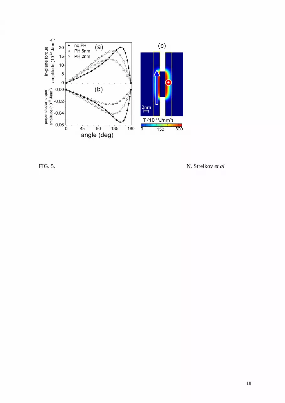
18
FIG 5 N Strelkov et al