Toward Spin-LED and Spin-VECSEL operations at magnetic ...
279
HAL Id: tel-01127040 https://tel.archives-ouvertes.fr/tel-01127040 Submitted on 6 Mar 2015 HAL is a multi-disciplinary open access archive for the deposit and dissemination of sci- entific research documents, whether they are pub- lished or not. The documents may come from teaching and research institutions in France or abroad, or from public or private research centers. L’archive ouverte pluridisciplinaire HAL, est destinée au dépôt et à la diffusion de documents scientifiques de niveau recherche, publiés ou non, émanant des établissements d’enseignement et de recherche français ou étrangers, des laboratoires publics ou privés. Toward Spin-LED and Spin-VECSEL operations at magnetic remanence Julien Frougier To cite this version: Julien Frougier. Toward Spin-LED and Spin-VECSEL operations at magnetic remanence. Other [cond-mat.other]. Université Paris Sud - Paris XI, 2014. English. NNT : 2014PA112175. tel- 01127040
-
Upload
khangminh22 -
Category
Documents
-
view
0 -
download
0
Transcript of Toward Spin-LED and Spin-VECSEL operations at magnetic ...

HAL Id: tel-01127040https://tel.archives-ouvertes.fr/tel-01127040
Submitted on 6 Mar 2015
HAL is a multi-disciplinary open accessarchive for the deposit and dissemination of sci-entific research documents, whether they are pub-lished or not. The documents may come fromteaching and research institutions in France orabroad, or from public or private research centers.
L’archive ouverte pluridisciplinaire HAL, estdestinée au dépôt et à la diffusion de documentsscientifiques de niveau recherche, publiés ou non,émanant des établissements d’enseignement et derecherche français ou étrangers, des laboratoirespublics ou privés.
Toward Spin-LED and Spin-VECSEL operations atmagnetic remanence
Julien Frougier
To cite this version:Julien Frougier. Toward Spin-LED and Spin-VECSEL operations at magnetic remanence. Other[cond-mat.other]. Université Paris Sud - Paris XI, 2014. English. NNT : 2014PA112175. tel-01127040

Université Paris-Sud
Ecole Doctorale 564:Physique en Île-de-France
Laboratoire: Unité Mixte de Physique CNRS/THALES
Discipline : Physique
Thèse de doctorat
Soutenue le 29 Septembre 2014
par
Julien FROUGIER
Towards Spin-LED and Spin-VECSEL
operation at magnetic remanence
Composition du Jury :
Directeur de thèse : Jean-Marie GEORGE Chargé de Recherche (UMϕ CNRS/Thales)
Rapporteurs : Angélique RISSONS Chargé de Recherche (ISAE)
Michael OESTREICH Professeur (University of Hannover)
Examinateurs : Ghaya BAILI Ingénieur (Thales Research & Technology)
Fabien BRETENAKER Directeur de Recherche (Laboratoire Aimé Cotton)
Stéphane MANGIN Chargé de Recherche (Institut Jean Lamour)


Acknowledgements
I would like to start by sincerely thanking the Prof. Angélique Rissons and theProf. Michael Oestreich for reviewing this thesis manuscript as well as Prof. FabienBretenaker and Dr. Stéphane Mangin for accepting to be members of my evaluationjury.
Thank you very much Yong Chang Lau, my friend and fellow INSA Toulouse grad-uate, for introducing me to the UMϕ sta as a candidate on this Ph.D Thesis.
Next, I would like to give a special thank to Dr. Jean-Marie George, Dr. GhayaBaili and Dr. Henri Jarès for trusting me and recruiting me on this Ph.D position.Thank you Jean-Marie for your supervision and your good humor throughout thosethree years. I appreciated the work freedom that you let to your students; this way offunctioning was the right one for me. Being able to learn without pressure is alwaysenjoyable. Thank you also for dealing so well with my "control freak syndrome" andhelping me in my Post-Doctoral Job search. I learned a lot at your contact and Ileave your team feeling ready to climb the next rung on the ladder: mission accom-plished. Thank you Ghaya for introducing me to the optics community but also forteaching and sharing with me your experimental expertise on VECSEL. Good jobon managing me when I was freaking out on deadlines and intense workloads. Andof course, congratulations again on your new "Young and Dynamic Mom" status!Thank you Henri for your scientic and human support throughout this Thesis. Youhave always been available when I needed it, ready to deliver your precious advices.Be sure that you stand out as a major participant in the success of this Thesis.Thank you also for helping me in my Post-Doctoral Job search.
Many thanks to Dr. Daniel Dol who initiated the Spin-VESCEL project and whoseamazing human and management qualities lead to a fruitful partnership between theUnité Mixte de Physique CNRS/Thales and Thales Research & Technology. Thankyou Daniel for always behind available when I needed advices and for helping me inmy Post-Doctoral job search.
I also want to thanks the Dr. Pascale Nouchi for actively participating in myrecruitment and introducing me to the optics division of Thales Research & Tech-nology. Thanks for your advices and for all the pleasant discussions about California,Florida and your US experience in general.
Many thanks to the project partners Dr. Mehdi Alouini (IPR), Dr. Isabelle Sagnes(LPN ) and Dr. Arnaud Garnache (IES ) for their tremendous work on the theoreti-cal and experimental development of Spin-VECSEL. Thank you Mehdi for applyingyour talent to the benet of the project and for being a continual source of bril-liant ideas and scientic intuition. Thank you Isabelle and Arnaud for the amazingstructures emerging from your partnership and for your availability throughout the

ii
project.
I would like to thanks all the members of the LPCNO 's Quantum Optoelectronicteam for their contribution to both the Spin-LED and the Spin-VECSEL projects.Thank you Prof. Pierre Renucci and Prof. Xavier Marie for inspiring me when Iwas still a student at the INSA Toulouse. Thank you Pierre for taking the time tocorrect part of this manuscript, I really appreciated it.
Thank you to all the members of Dr. Yuan Lu's team (Institut Jean-Lamour) fortheir contribution to both the Spin-LED and the Spin-VECSEL projects. Thankyou Yuan for your help, advices and legendary eciency throughout those threeyears. Your outstanding management skills combined with your scientic passionlead to remarkable developments on both the SISTER and the INSPIRE projects.
Thanks to the Lab's managing trinity: the Prof. Dr. and 2007 Nobel LaureateAlbert Fert for his kindness, modesty, scientic inspiration and support in my Post-Doctoral job search, Dr. Frédéric Nguyen Van Dau for his scientic advices andknowledge, and Dr. Frédéric Petro for running the Lab like clockwork.
Another special thanks to Dr. Nicolas Reyren, the man whose knowledge is onlyequaled by his unshakeable good mood. Your passion for science, extraordinarysense of Physics and human qualities always makes it enjoyable to work by yourside. Do not change anything you got the winning recipe! Thank you for correct-ing part of this manuscript and for helping with the corrections of my rst paper.Thank you also for all the little helps and advices given here and there that madea huge dierence all the time. I hope that I will get the opportunity to work withyou again in a near future.
Thanks to Dr. Michael Tran and Dr. Julian Peiro, two ocial JMG-Boys Clubmembers, for helping me on my arrival, introducing me to the lab and making mefeel home. Thank you Michael for your precious cleanroom training and for youramazing joy of living. Thank you Julian for all your advices, countless helps andpriceless discussions about your already legendary optimism.
I also would like to thanks the team of the III-V lab for letting me access theircleanroom during these three years and use their lithography equipment. Manythanks to Bouzid Simourad, Marco Lamponi and Dr. Gregory Maisons for theirhelp, advices and impressive problem solving skills. You made me feel home in theIII-V cleanroom and I really appreciated it. Don't change anything, you guys rock!
Thank you Dr. Gilles Feugnet for your help, expertise and advices during the longhours I spent struggling on the extended laser cavity. I really appreciated your senseof humor and your capacity to always minimize the seriousness of the problems faced.
iii
Special thanks to "CEO" Cyrile Deranlot, the man who rubs shoulders with successon a daily basis. An uncompromised professionalism and exemplary human values,I am really happy I got to know you during these three years at the UMϕ. Goodluck in your new adventure. "Work seriously without taking yourself seriously!"
BACK IN THE GYM!!! With Edouard Lesne and Ryan Cheri, a.k.a Lord Ed andLord Ryan, a.k.a Trapzilla and Quadzilla,...a.k.a Bishop Gains and Bishop Shreds!Thank you guys for the awesome training sessions we spent making ALL KINDSOF GAINS! All kinds· · · But also for the priceless moments we spent optimizingthe anabolic window by eating tons and tons of food. I am really glad I got to meetyou guys during my stay at the UMϕ. Let's keep it clean brahs: Go Hard or GoHome, Curls for the girls and of course one more rep' for the Sparta!
Thank you Dr. Nicolas Locatelli for your brilliant advices throughout these threeyears, both on the scientic and administrative sides. I really enjoyed interactingwith you and hope that I will continue seeing you around.
Merci à Eric Jacquet, l'homme ayant détrôné George Abitbol au titre de l'hommele plus classe du monde. Je prends l'initiative d'écrire ces remerciements en françaiscar je sais que l'anglais n'est pas (encore) ta langue favorite. Merci pour tes coupsde mains, tes dépannages de matériels et tes discussions sportives. Toujours unplaisir de te croiser dans un couloir ou de t'entendre tailler un costard (toujours surmesure) à une victime innocente! Ne change rien, tu es royal!
Je souhaite également sincèrement remercier Christine Marchand-Goudroye et AnneDussart, véritable travailleuses de l'ombre à l'ecacité inégalable, pour leur remar-quable assistance quotidienne tout au long de ces trois années. Votre gentillesse etvos sourires amicaux n'ont jamais manqué d'illuminer mes journées. Merci Mes-dames!
I also would like to thank the rest of the lab: Ph.D Students, Ph.Ds and Engi-neers who might not be mentioned above but whose daily assistance, support andfriendship helped me to successfully complete this Thesis.
Je remercie très sincèrement ma famille pour avoir cru en moi, supporté et encour-agé depuis le début de ces longues études. Merci à mes parents, Michel et Annette,de toujours avoir fait votre maximum pour assurer la réussite de votre progéniture.Merci à ma soeur Claire pour son soutien, pour avoir brillamment supporté moncaractère pas toujours évident et pour m'avoir fait redescendre sur terre quand lebesoin s'en faisait sentir.
Of course, I also would like to thanks my close friends Victor, Val, Emilien, Jeremy,Sylvain, Aurélien, Pierre and Chloé for their unconditional support since we met inHigh School or over the years.

iv
Finally, I will conclude by thanking a very special lady, Jennifer Castiblanco, whohas always been there for me during the past four years. 5 feet 2 of highly concen-trated awesomeness always mentally by my side despite the geographical remoteness.Thank you so much for your unconditional support and daily encouragements. Nowthat this chapter is over, I can't wait to start the next one with you, in the US andphysically present by your side. Thank you for your patience, mental strength andkindness. You are the best.

Contents
1 Introduction: The Rise of Semiconductor Spintronics 1
1.1 Context and motivations . . . . . . . . . . . . . . . . . . . . . . . . . 21.2 The Manuscript . . . . . . . . . . . . . . . . . . . . . . . . . . . . . . 6
2 Conversion of a magnetic information into light polarization infor-
mation using spin-injected III-V semiconductors 9
2.1 Spin injection into semiconductors . . . . . . . . . . . . . . . . . . . 112.1.1 Theoretical study of spin injection . . . . . . . . . . . . . . . 13
2.1.1.1 Electronic transport: Boltzmann Model . . . . . . . 132.1.1.2 Concept of spin accumulation at a single F/N interface 142.1.1.3 Extension to multilayers problems (F/N)m: Valet-
Fert Model . . . . . . . . . . . . . . . . . . . . . . . 172.1.1.4 Ecient spin injection in a semiconductor: Fert-
Jarès Model . . . . . . . . . . . . . . . . . . . . . . 212.1.2 Generation of a spin-polarized carriers in a semiconductor . . 29
2.1.2.1 Electrical spin-injection from a ferromagnetic metals 292.1.2.2 Generation of spin accumulation: Beyond direct spin
injection . . . . . . . . . . . . . . . . . . . . . . . . 382.1.3 Spin-Orbit interaction and Spin relaxation mechanisms . . . . 44
2.1.3.1 Dyakonov-Perel . . . . . . . . . . . . . . . . . . . . 442.1.3.2 Elliot-Yafet . . . . . . . . . . . . . . . . . . . . . . . 462.1.3.3 Bir-Aronov-Pikus . . . . . . . . . . . . . . . . . . . 462.1.3.4 Hyperne interaction . . . . . . . . . . . . . . . . . 472.1.3.5 Spin relaxation in conned potentials: QW and QD 47
2.2 From matter to light: Conversion of spin accumulation into lightpolarization information . . . . . . . . . . . . . . . . . . . . . . . . . 492.2.1 Optical detection of a spin-polarized current in a III-V semi-
conductor . . . . . . . . . . . . . . . . . . . . . . . . . . . . . 492.2.1.1 General properties of III-V semiconductors . . . . . 502.2.1.2 Spin information conversion through quantum opto-
electrical mechanism . . . . . . . . . . . . . . . . . . 532.2.1.3 Circularly-Polarized Optical Pumping . . . . . . . . 562.2.1.4 Design of spin-polarized light sources . . . . . . . . 592.2.1.5 Measurements considerations . . . . . . . . . . . . . 61
2.2.2 The Spin-LED concept . . . . . . . . . . . . . . . . . . . . . . 662.2.2.1 n-i-p band structure . . . . . . . . . . . . . . . . . . 662.2.2.2 State-of-the-art . . . . . . . . . . . . . . . . . . . . . 672.2.2.3 Application limits: Towards spin injection in LASER
systems . . . . . . . . . . . . . . . . . . . . . . . . . 69

vi Contents
2.2.3 Spin injection into semiconductor laser structures . . . . . . . 712.2.3.1 Description and properties of VCSELs . . . . . . . . 712.2.3.2 Spin-VCSEL: Operation Principal and Analytical Model 722.2.3.3 Polarization dynamics of VCSEL: The Spin Flip Model 782.2.3.4 Interest, Stakes and Applications . . . . . . . . . . . 932.2.3.5 State-of-the-art . . . . . . . . . . . . . . . . . . . . . 94
3 Development and optimization of an ultra-thin MgO/CoFeB/Ta
spin-injector with perpendicular magnetization. 97
3.1 Spin-LEDs structures and Photolithography process . . . . . . . . . 993.1.1 Spin-LEDs structures . . . . . . . . . . . . . . . . . . . . . . 993.1.2 Sample preparation . . . . . . . . . . . . . . . . . . . . . . . . 100
3.2 Optimization of the MgO Tunnel Barrier: MBE vs. Sputtering growth1023.2.1 Samples preparation . . . . . . . . . . . . . . . . . . . . . . . 1023.2.2 Impact of annealing on the MgO/CoFeB bi-layer . . . . . . . 1033.2.3 Role of the GaAs/MgO and MgO/CoFeB interfaces . . . . . . 108
3.3 Development of an ultra-thin MgO/CoFeB spin-injector with Perpen-dicular Magnetic Anisotropy . . . . . . . . . . . . . . . . . . . . . . . 1123.3.1 Physical origins of Perpendicular Magnetic Anisotropy in ultrathin-
ferromagnetic-lms . . . . . . . . . . . . . . . . . . . . . . . . 1123.3.2 Sample preparation and structural characterization . . . . . . 1183.3.3 Magnetic properties of the spin-injector . . . . . . . . . . . . 1203.3.4 Perpendicular Magnetic Anisotropy of MgO/CoFeB bi-layer . 1213.3.5 Measurements and characterization . . . . . . . . . . . . . . . 123
3.4 Limits and Perspectives . . . . . . . . . . . . . . . . . . . . . . . . . 132
4 Spin injection into Vertical External Cavity Surface Emitting Lasers135
4.1 Description and properties of VECSEL . . . . . . . . . . . . . . . . . 1394.1.1 Device . . . . . . . . . . . . . . . . . . . . . . . . . . . . . . . 1394.1.2 Pumping methods . . . . . . . . . . . . . . . . . . . . . . . . 1394.1.3 Temperature control . . . . . . . . . . . . . . . . . . . . . . . 1414.1.4 Applications . . . . . . . . . . . . . . . . . . . . . . . . . . . . 141
4.2 Designs and characteristics of the structure . . . . . . . . . . . . . . 1434.2.1 General considerations . . . . . . . . . . . . . . . . . . . . . . 1434.2.2 Optically Pumped Structures . . . . . . . . . . . . . . . . . . 1454.2.3 Electrically Pumped Structures . . . . . . . . . . . . . . . . . 146
4.3 Vectorial Analysis of spin-injected VECSEL . . . . . . . . . . . . . . 1494.3.1 Inuence of birefringence and dichroism on the polarization
selection . . . . . . . . . . . . . . . . . . . . . . . . . . . . . . 1494.3.1.1 Mathematical formalism . . . . . . . . . . . . . . . . 1494.3.1.2 Identication of the oscillation regimes . . . . . . . . 1524.3.1.3 Synthesis and conclusion . . . . . . . . . . . . . . . 157
4.3.2 Preparation of the laser eigen state . . . . . . . . . . . . . . . 1594.3.2.1 Intra-cavity Faraday rotator . . . . . . . . . . . . . 159

Contents vii
4.3.2.2 New oscillation regimes . . . . . . . . . . . . . . . . 1614.3.2.3 Synthesis and conclusion . . . . . . . . . . . . . . . 163
4.4 Birefringence measurements . . . . . . . . . . . . . . . . . . . . . . . 1654.4.1 Introduction . . . . . . . . . . . . . . . . . . . . . . . . . . . . 1654.4.2 Experimental setup . . . . . . . . . . . . . . . . . . . . . . . . 1664.4.3 Identication of the two linearly-polarized orthogonal modes . 1694.4.4 Birefringence measurements . . . . . . . . . . . . . . . . . . . 1694.4.5 Discussion . . . . . . . . . . . . . . . . . . . . . . . . . . . . . 172
4.5 Optically spin-injected VECSELs . . . . . . . . . . . . . . . . . . . . 1754.5.1 Linear-Cavity VECSEL . . . . . . . . . . . . . . . . . . . . . 175
4.5.1.1 Experimental Setup . . . . . . . . . . . . . . . . . . 1754.5.1.2 Experimental observations . . . . . . . . . . . . . . 176
4.5.2 Extended M-Cavity VECSEL . . . . . . . . . . . . . . . . . . 1774.5.2.1 Experimental Setup . . . . . . . . . . . . . . . . . . 1774.5.2.2 Experimental observations . . . . . . . . . . . . . . 179
4.5.3 Analysis of the physical mechanisms: The Lamb model . . . . 1794.5.3.1 Mathematical formalism . . . . . . . . . . . . . . . . 1804.5.3.2 Synthesis and conclusions . . . . . . . . . . . . . . . 182
4.6 Discussion on the characteristic lifetimes . . . . . . . . . . . . . . . . 1864.6.1 Radiative lifetime dynamics in a laser . . . . . . . . . . . . . 1864.6.2 Time-Resolved Photo-Luminescence measurements . . . . . . 1894.6.3 Data comparison and partial conclusion . . . . . . . . . . . . 195
4.7 Electrically spin-injected VECSELs . . . . . . . . . . . . . . . . . . . 1984.7.1 Insertion of an Intra-Cavity spin-injector . . . . . . . . . . . . 1984.7.2 Deposition of a spin-injectors with Perpendicular Magnetic
Anisotropy on a 12 -VCSEL . . . . . . . . . . . . . . . . . . . . 199
5 Overall Conclusion 203
5.1 Development of a new ultra-thin spin-injector . . . . . . . . . . . . . 2035.2 Summary on spin-injection into VECSELs . . . . . . . . . . . . . . . 2045.3 Perspectives, challenges and future applications . . . . . . . . . . . . 208
A Complementary calculation related to spin-injection into semicon-
ductors 215
A.1 Formal demonstration of the General Boltzmann equation . . . . . . 215A.2 Valet-Fert Model: Expressions of the electrochemical potentials and
the associated currents . . . . . . . . . . . . . . . . . . . . . . . . . . 218A.3 Valet-Jarès Model: Expressions of the electrochemical potentials
and the associated currents . . . . . . . . . . . . . . . . . . . . . . . 219
B Spin Flip Model - Single mode emission: Basic polarization states221
C Micro-pillar photolithography process 225

viii Contents
D Formal demonstration of the relation between frequency detuning
and birefringence 227
E Complementary information on TRPL measurements 231
E.1 Experimental setup . . . . . . . . . . . . . . . . . . . . . . . . . . . . 231E.2 Band-to-band transitions and excitation energies of the InGaAs/GaAsP
12 -VCSEL . . . . . . . . . . . . . . . . . . . . . . . . . . . . . . . . . 232
E.3 Complementary TRPLmeasurements of the InGaAs/GaAsP GaAs61512 -VCSEL . . . . . . . . . . . . . . . . . . . . . . . . . . . . . . . . . 233
F List of Publications 235
G List of Conferences 237
Bibliography 239

List of Acronyms
A.
• AO-HDS: All Optical-Heliticity Dependent Switching
• ASE: Amplied Spontaneous Emission
B.
• BAP: Bir-Aronov-Pikus
C.
• CB: Conduction Band
• CESR: Conduction Electron Spin Resonance
• CIP: Current-In-Plane
• CMOS: Complementary Metal-Oxide Semiconductor
• CNT: Carbon Nano-Tube
• CPO: Coherent Population Oscillation
• CPP: Current Perpendicular to the Plane
• CPT: Coherent Population Trapping
• CW: Continuous Wave
D.
• DBR: Distributed Bragg Reector
• DFT: Density Functional Theory
• DMS: Diluted Magnetic Semiconductor
• DoCP: Degree of Circular Polarization (Also identied as Pc or Pcirc)
• DOS: Density Of State
• DP: Dyakonov-Perel (Spin relaxation mechanism)

x Contents
E.
• EL: Electro-Luminescence
• ESA: Electrical Spectrum Analyzer
• EY: Elliot-Yafet (Spin relaxation mechanism)
F.
• FFT images: Fast Fourier Transform images
• F/N: Ferromagnetic/Non-magnetic metal
• F/SC: Ferromagnetic/Semiconductor
• F/I/SC: Ferromagnetic/Insulator/Semiconductor
• F/T/SC: Ferromagnetic/Tunnel/Semiconductor
• FP: Fabry-Perot (Interferometer)
• FSR: Free Spectral Range
G.
• GCD: Gain Circular Dichroism
• GMR: Giant Magneto-Resistance
H.
• HEMFET: High-Electron-Mobility-Field-Eect-Transistor
• HEMT: High-Electron-Mobility-Transistor
• HH: Heavy Hole (Valence Band)
• HMF: Half-Metallic Ferromagnet
• HR-TEM: High Resolved-Transmission Electron Microscopy
I.
• ISHE: Inverse Spin-Hall Eect
• ITRS: International Technology Roadmap for Semiconductors

Contents xi
J.
K.
L.
• LASER: Light Amplication by Stimulated Emission Radiation
• LED: Light Emitting Diode
• LH: Light Hole (Valence Band)
• LIDAR: LIght Detection and Ranging
M.
• MA: Magnetic Anisotropy
• MBE: Molecular Beam Epitaxy
• MCD: Magnetic Circular Dichroism
• MOCVD: Metal-Organic Chemical Vapor Deposition
• MQW: Multiple Quantum Wells
• MRAM: Magnetic Random Access Memory
• MTJ: Magnetic-Tunnel-Junction
N.
O.
P.
• PD: Photo-Diode
• PL: Photo-Luminescence
• PMA: Perpendicular Magnetic Anisotropy
Q.
• QW: Quantum Well

xii Contents
R.
• RGB light source: Red-Green-Blue light source
• RHEED: Reection High Energy Electron Diraction
• RT: Room Temperature
• RTA: Rapid Thermal Annealing
S.
• SFM: Spin-Flip Model
• SHE: Spin-Hall Eect
• SO: Spin-Orbit
• SQUID: Superconducting Quantum Interference Device Magnetometer
• SSE: Spin-Seebeck Eect
• STT: Spin-Transfer-Torque
• STT-MRAM: Spin Transfer Torque-Magnetic Random Access Memory
T.
• TE: Transverse Electric (Polarization mode)
• TEGFET: Two-dimensional-Electron-Gas-Field-Eect-Transistor
• TM: Transverse Magnetic (Polarization mode)
• TMR: Tunnel Magneto-Resistance
• TRPL: Time Resolved Photo-Luminescence
U.
V.
• VB: Valence Band
• VCSEL: Vertical Cavity Surface Emitting Laser
• VECSEL: Vertical External Cavity Surface Emitting Laser

Contents xiii
W.
X.
• XH: Heavy Exciton
Y.
• YAG: Yttrium Aluminum Garnet
Z.


Chapter 1
Introduction: The Rise of
Semiconductor Spintronics
Contents
1.1 Context and motivations . . . . . . . . . . . . . . . . . . . . . 2
1.2 The Manuscript . . . . . . . . . . . . . . . . . . . . . . . . . . 6
Spintronics describes a paradigm where the information is carried by the elec-tron spin instead of its charge like in mainstream electronics. This oers oppor-tunities for a new generation of devices combining standard microelectronics withspin-dependent eects arising from the interaction between the electrons' spin andthe magnetic properties of the material.
The discovery of the Giant Magneto-Resistance (GMR) by Albert Fert [1] and PeterGrunberg [2] in 1988, both awarded the Nobel Prize in 2007, revealed the tremen-dous potential of spintronics for technological applications. In the consecutive yearsimportant research eorts toward the control and manipulation of the electron spinin various systems have been displayed. Fields of studies such as Tunnel Magneto-Resistance (TMR) [3, 4, 5], Spin Transfer Torque oscillators [6] and spin injectionin metals [7], semiconductors [8], graphene [9, 10], Carbon Nano-Tubes (CNT) [11]and other organic materials emerged [12, 13, 14] . Impressive R&D achievementsenabled to rapidly reach a high technological maturity for the rst spintronic basedhardware devices [15] leading to the commercialization of hard drives using GMR(IBM, 1997) and TMR (Seagate, 2006), GMR-based galvanic isolators, MagneticRandom Access Memories (MRAM) and in a near future the Spin Transfer TorqueRandom Access Memories (STT-RAM).Nevertheless, spintronics present the paradox of being one of the best non-volatilestorage technology available while in the meantime the spin information is highlyvolatile when transported. Even if the science and technology behind passive spin-tronic devices is well mastered today, the realization of active devices such as Spin-Transistors or Spin-Lasers remains a great challenge. The intense research towardsthe creation of such components are motivated by the potentiality of combiningmagnetic storage of information with electronic readout in a single device. In thecase of Spin-Lasers for instance, one could envisage to propagate the informationcontained in a magnetic bit over kilo-metric distances after converting the spin-

2 Chapter 1. Introduction: The Rise of Semiconductor Spintronics
information onto the polarization of the emitted light. On the other hand, Spin-Transistors could lead to computers in which the distinction between active andpassive memory has been removed and in which the data is processed in the samepart of memory in which it is stored [16]. Therefore, this eld of condensed matterphysics represents one of the great potential alternative to overcome the predictedlimits of conventional electronics in a near future.
1.1 Context and motivations
Spin-polarized electron injection into semiconductors has been a eld of growinginterest for the past two decades. From a technological transfer point of view, itis probably the most promising path to explore regardless of the existing micro-electronic industry dynamic. The injection, transport, manipulation and detectionof spins in such materials are the four key points to master in the future to create anactive spin-based device. The Spin-High Electron Mobility Field Eect Transistor(HEMFET) proposed by Datta et Das [17] is a great conceptual illustration of whatcould be achieved with this technology (Figure 1.1).
Ferromagnetic
electrodes
Gate
electrode
Spin polarized
electrons 2DEG
𝐵 𝑒𝑓𝑓𝑒𝑐𝑡𝑖𝑣𝑒 =𝑝 × 𝐸
2𝑚𝑐2
Coherent Spin-flip
by Rashba Effect
E
Figure 1.1: Conceptual illustration of Datta et Das Spin-HEMFET [17]. In a spin-
FET, spin-polarized electrons are injected from a ferromagnetic source into a semicon-
ductor and detected using a ferromagnetic drain electrode. The coherent spin-ip of
the 2D-Electron Gas (2DEG) in the channel can be controlled by the Rashba Eect
emerging from the Spin-Orbit interaction [18].
Spin-Transistors, classied by the ITRS as "Non-Conventional Charge-based Ex-tended CMOS Devices", are one of the considered options for the post-CMOS era.Spin-based transistors that do not strictly rely on the raising or lowering of elec-trostatic barriers can overcome scaling limits in charge-based transistors [19, 20].Spin transport in semiconductors might also lead to dissipation-less informationtransfer with pure spin currents [21]. Adding the spin degree of freedom to conven-tional semiconductor charge-based electronics will add substantially more capabilityand performance to electronic products [15]. The advantages of these new devices

1.1. Context and motivations 3
would be non-volatility, increased data processing speed, decreased electric powerconsumption and increased integration densities compared with conventional semi-conductor devices [15]. Dierent compounds such as IV-IV semiconductors (Si,Ge) [22, 23, 24, 25] and III-V semiconductors (GaAs, InAs) [26] have already beenstrongly investigated. When thinking about minimizing technological transfer chal-lenges, one probably envisages using Si as transport medium. Indeed it would bevery interesting to get conclusive results with this material and take advantage, forfuture R&D, of the unmatched technological maturity developed by the multi-billiondollars microelectronic industry built around silicon. The rst electrical measure-ments in Si showed a high potential for spin transport with a relatively long spinlifetime and a non-local spin signal detectable up to 500 K [27].
Figure 1.2: General overview of spin-based electronic devices. As opposition with
the Spin-FET, in a spin-LED the spin injection eciency is probed by measuring
circularly polarized light emission occurring under spin injection. Figure adapted from
reference [28]
Nevertheless, when it comes to the study of spin-injection in semiconductors,III-V compounds also provides really interesting and attractive properties. Binary(GaAs, InP, GaN) and Ternary (InGaAs, GaAsP) III-V semiconductors are alreadywidely used in optoelectronics as base materials for light sources and detectors.Their direct gap enables radiative recombination of the injected carriers. Moreover,the mastering of III-V epitaxy lead to competitive development of high electron

4 Chapter 1. Introduction: The Rise of Semiconductor Spintronics
mobility transistors (HEMT, HEMFET, TEGFET) which are massively used inhyper-frequency data treatment (cellphones, satellite telecommunications). In thepast decade, a continuous interest and a research eort have been dedicated to thestudy of spin-injection into III-V semiconductor based Light Emitting Device suchas Spin-Light Emitting Diodes (Spin-LEDs). The rst functional Spin-LED wasproposed by Fiederling et al. in 1999 [29]. This experimental demonstration openedthe door to a new eld of study: the opto-spintronics.
In Spin-LEDs (Figure 1.2), the spin information of the injected electrons can be con-verted into circular polarization information carried by the emitted photons. Thisinformation transfer happens through the optical quantum selection rules for dipoleradiation associated with the conservation of angular momentum z-projections mz
occurring in conned strained active medium or Quantum Wells (QWs) [30]. Thisresults in an emission of right- or left-circularly polarized photons depending on theelectrons' spin orientation. Encouraging results were already obtained with elec-trically injected Spin-LEDs in applied magnetic eld at cryogenic temperatures.Nevertheless, such spin-optoelectronic devices will be competitive for realistic appli-cations only if the spin-injection can be performed electrically at room temperaturewithout an applied magnetic eld. Additionally, the device must provide a coherentlight emission with switchable polarization state and an output polarization degree(Pc) as high as possible in order for instance to robustly encode a bit of information.
In recent years, Spin-LASERs came out as a potential solution by proposing higherand promising performances in terms of emission coherence (spatially and tempo-rally), output Degree of Circular Polarization (DoCP) and room temperature oper-ation as compared to Spin-LEDs. The amplication eects induced by the combi-nation of a gain medium and a resonant optical cavity give a unique opportunity tomaximize the conversion eciency of the carrier spin-information into light polar-ization information. Such Spin-LASERs would provide a number of advantages overconventional VCSELs for future optical communication systems such as spin drivenrecongurable optical interconnects [31, 32, 33], fast modulation dynamics [34, 35],polarization control [36, 37] as well as higher performances such as laser thresh-old reduction [37, 38, 39], improved laser intensity, and polarization stability. Theideas emerging from Spin-LASERs and polarization switching may also motivateother device concepts like, for example, cryptography, coherent detection systemsor magneto-optical recording [40].
In terms of device implementation, III-V semiconductor based Vertical Cavity Sur-face Emitting Lasers (VCSEL) emerged as perfect candidates for a Spin-Laser im-plementation thank to their vertical geometry (Figure 1.3(a)). Additionally, theyexhibit a polarization emission much more isotropic than the conventional side-emitting laser diodes. Outstanding optical [36, 41, 42, 43] and electrical [37, 44]spin-injection results were already achieved in monolithic VCSEL structures in thepast few years. However, VCSEL also exhibit intrinsic limitations in terms of noise

1.1. Context and motivations 5
(a)
External Cavity
Output Coupler
λ
Intra-Cavity Ferromagnetic
Spin-Injector
(b)
Figure 1.3: Comparison between a monolithic-VCSEL and a VECSEL: (a)
Conceptual scheme of a Spin-injected Vertical Cavity Surface Emitting Laser. Figure
reprinted from [45]. (b) Illustration of a Vertical External Cavity Surface Emitting
Laser based on a 12 -VCSEL chip. The ferromagnetic spin-injector is deposited inside
the external cavity on top of the structure.
performances due to their Class-B behavior, output power and also device exibil-ity. Indeed, from a fundamental study viewpoint, their compact monolithic designusually standing as a major asset when it comes to application becomes a hindrancefor the exploratory approach of spin-injection in lasers with vertical geometries. Inparticular, when considering electrical spin-injection, the classic VCSEL architec-ture with the annular top electrode deposited on the top Distributed Bragg Reector(DBR) far from the active medium is not optimal. To maximize the spin-injection ef-ciency in optoelectronics devices, a general rule is to minimize the distance betweenthe spin-injector and the active medium of the structures; where radiative recombi-nations occur in order to minimize the spin-relaxation during electronic transport.Fortunately, Vertical External Cavity Surface Emitting Lasers (VECSEL) based on12 -VCSEL oer eective solutions to overcome these problems.

6 Chapter 1. Introduction: The Rise of Semiconductor Spintronics
1.2 The Manuscript
This Ph.D thesis proposes to explore this new paradigm of spin-information propa-gation over very long distances after encoding on coherent light polarization. Thisrecent multidisciplinary theme, at the interface of Semiconductors, Magnetism andPhotonics (Figure 1.2), still present to this day great understanding and technolog-ical challenges. While so far all the Spin-Laser experiments have been performedusing monolithic VCSEL, we decided during this Ph.D to explore an alternative pathby focusing on the study of optical and electrical spin-injection in VECSEL (Figure1.3(b)). Hereinafter, the term 1
2 -VCSEL describes a monolithic VCSEL where thetop DBR has been taken o and characterizes the semiconductor chip itself. How-ever, the term VECSEL denes the whole laser itself where the 1
2 -VCSEL has beencompleted with a conventional mirror to create an external cavity (Figure 1.3(b)).
VECSEL devices combine wavelength versatility and potential for high output powerwith a high beam quality. Moreover, they stand out as a perfect tool for the inves-tigation of fundamental physics by allowing the insertion of additional intra-cavityoptical components to modify the laser's behavior. They already demonstrated ul-trashort pulses generation with modelocking using semiconductor saturable absorbermirrors (SESAM) [46, 47, 48, 49, 50, 51] and also intracavity frequency doublingby inserting a nonlinear crystal into the laser resonator. VECSEL are of great in-terest for Thales which needs to acquire increasingly sophisticated technologies. Inparticular for detection, analysis and decision-making technology, in order to designand develop critical information systems. Dual-frequency VECSEL could stand outas innovative solutions in the elds of secure military communications, space sys-tems, air trac control but also on-board electronics and government informationnetworks. They emit two orthogonally-polarized coherent beams with a frequencydetuning between the modes that can be precisely adjusted from few MHz to fewTHz [52]. Optical sources with low noise-level are also required for applicationssuch as optical-ber sensing, cryptography and microwave photonics [53]. In termsof electrical spin-injection, the elimination of top DBR in 1
2 -VCSEL oers the uniqueadvantage to deposit a spin-injector on top of the structure as close as possible tothe QWs (Figure 1.3(b)). Using this technique maximizes the spin polarization de-gree reaching the active medium by taking advantage of a spin diusion length lsflonger than the distance between the injector and the QWs.
Many challenges and interrogations emerged from this ambitious and innovativeproject which among these: What major physical parameters control the spin-injection in VECSEL? Can the injection of spin-polarized carriers overpower thelinear birefringence and set the device polarization? How can we evaluate the con-version eciency of the spin-information onto the emitted light polarization? Forthe electrical spin-injection, is it possible to develop a spin-injector with Perpendic-ular Magnetic Anisotropy at magnetic remanence for room temperature operationfree of any applied magnetic eld? Also, will the VECSEL tolerate the important

1.2. The Manuscript 7
losses induced by a highly absorbent ferromagnetic spin-injector deposited intra-cavity?
All these challenges will be addressed in this manuscript. The investigation willbe divided into three major chapters. The subject of this thesis being at the in-terface of Spintronics, Photonics, Semiconductor Physics and Material Science, thismanuscipt is addressed to a wide range of readers having completely or partiallydierent backgrounds. Consequently, I made the personal choice to develop an ex-haustive State-of-the-art (second chapter) where most of the informations requiredto fully appreciate this highly multi-disciplinary subject can be found. Additionally,as the Spin-VECSEL project started with my Ph.D thesis, one of the manuscript'srst vocation is to lay a solid foundation for the good continuation of the project.Consequently, depending on the reader background and knowledge, one should feelfree to skip some sections in the rst part if the need arises. The presentation of theexperimental work performed during this Ph.D thesis starts page 101 and is fullydescribed in the second and the third and fourth chapters of this manuscript.
The second chapter regroups a state-of-the-art of spin-injection into III-V semi-conductors optoelectronics devices and focuses on the physical phenomena engagedin the conversion of a spin accumulation into light polarization information. Asa preliminary, we start by discussing spin-injection and spin-transport into III-Vsemiconductor structures. Then, we develop the reference models on spin-injectionas well as the state-of-the-art methods to generate a spin accumulation. Following,we detail the several spin relaxation mechanisms originating from spin-orbit interac-tion. Then, a more device-oriented review is conducted by focusing on spin-injectionin Light Emitting Diodes (LEDs) and Vertical Cavity Surface Emitting Lasers (VC-SELs). A special attention is given to the understanding of Spin-VCSELs by intro-ducing an analytical analysis and a polarization dynamic model of such systems.
The third chapter is articulated around our experimental work on the developmentand the optimization on III-V semiconductors LEDs of an ultra-thin MgO/CoFeB/Taspin-injector with perpendicular magnetization at magnetic remanence. The fun-damental comprehension and the material mastering that emerged from this workstood out as a prerequisite for our work on Spin-LASERs. We rst start with ageneral discussion on Spin-LEDs and their fabrication by photolithography process.Then we focus on the optimization of the MgO tunnel barrier for maximizing thespin-injection eciency. Next, we will detailed the development and the characteri-zation of a MgO(2.5nm)/CoFeB(1.2nm)/Ta(5nm) spin-injector with perpendicularmagnetization at remanence. Finally, we conclude on the results and the limitsbrought to light by this research and further introduce spin-injection in lasers as apotential solution for overcoming the intrinsic limitation of Spin-LEDs.In this highly collaborative project, the LED structures were grown by Molecu-lar Beam Epitaxy (MBE) at the Key Laboratory of Semiconductor Materials Sci-ence (Beijing, CHINA) by Prof. B. Xu's team. The ferromagnetic Metal-Tunnel-
8 Chapter 1. Introduction: The Rise of Semiconductor Spintronics
Junction (MTJ) spin-injector were deposited and annealed at the Institut Jean-Lamour (Nancy, FRANCE) by Dr. Y. Lu's team. The devices characterization byTime Resolved Photo-Luminescence (TRPL) were performed at the Laboratoire dePhysique et de Chimie des Nano-Objet (Toulouse, FRANCE) by Dr. P. Barate inthe team of Prof. Pierre Renucci and Prof. Xavier Marie. I had the luck to becordially invited by the LPCNO's team to familiarize myself with the experimentalsetup and participate to some of the TRPL measurements. For this project, I wasin charge of the Spin-LEDs fabrication by photolithography process at Thales Re-search & Technology (Palaiseau, FRANCE) and I also took part to the analyze andinterpretation of the data.
The forth chapter contains the main part of this thesis work. It is fully dedicated toour experimental work on spin-injection in Vertical External Cavity Surface Emit-ting Laser structures. Following a general introduction on VECSEL devices, we walkthrough a vectorial analysis allowing the theoretical understanding of polarizationselection in spin-injected VECSELs. Next, we report birefringence measurements ofa VECSEL designed for optical pumping using an original frequency detuning mea-surement between the two orthogonal TE- and TM-modes. Afterward, we present,analyze and commente our observations and results on optical spin injection in VEC-SELs. The study is farther extended to the characterization of the ratio betweenthe carriers spin-lifetime τs and the carriers recombination time τ using TRPL mea-surements in order to evaluate the spin-information conversion eciency. Finally,we discuss the preliminary results of our experiments on electrical spin-injection.This project also involves a lot of partnerships. All the 1
2 -VCSEL structures usedduring this Ph.D thesis are the result of a fruitful collaboration between Dr. A. Gar-nache from the Institut d' électronique du Sud (Montpellier, FRANCE) and Dr. I.Sagnes from Laboratoire de Photonique et Nanostructures (Marcoussis, FRANCE).The designs and simulations of the structures are rst performed by the Dr. A.Garnache and the growths are realized using Metal-Organic Chemical Vapor De-position (MOCVD) by the Dr. I. Sagnes and the Dr. G. Beaudoin. The vectorialmodel has been developed by the Dr. M. Alouini from the Insitut de Physique deRennes (Rennes, FRANCE). The measurement of the VECSEL's spin-lifetime andcarrier-lifetime by TRPL are performed at the Laboratoire de Physique et de Chimiedes Nano-Objet (Toulouse, FRANCE) by Dr. P. Barate while the k.p simulationsof the 1
2 -VCSEL structure presented in Chapter 13 are realized by Prof. X. Marie.At Thales Research Technology, under the co-supervision of Dr. G. Baili and Dr.J. -M. George, I performed all the experimental investigations related to the opticaland electrical spin-injection in VECSEL structures.

Chapter 2
Conversion of a magnetic
information into light polarization
information using spin-injected
III-V semiconductors
Contents
2.1 Spin injection into semiconductors . . . . . . . . . . . . . . . 11
2.1.1 Theoretical study of spin injection . . . . . . . . . . . . . . . 13
2.1.2 Generation of a spin-polarized carriers in a semiconductor . . 29
2.1.3 Spin-Orbit interaction and Spin relaxation mechanisms . . . 44
2.2 From matter to light: Conversion of spin accumulation into
light polarization information . . . . . . . . . . . . . . . . . . 49
2.2.1 Optical detection of a spin-polarized current in a III-V semi-
conductor . . . . . . . . . . . . . . . . . . . . . . . . . . . . . 49
2.2.2 The Spin-LED concept . . . . . . . . . . . . . . . . . . . . . . 66
2.2.3 Spin injection into semiconductor laser structures . . . . . . . 71
Introduction
In this rst chapter we introduce the state-of-the-art knowledge related to spin-injection into semiconductor Light Emitting Diodes (Spin-LEDs) and Vertical (Ex-ternal) Cavity Surface Emitting Lasers (Spin-V(E)CSELs). The goal is to put inplace a granite foundation in order to better understand the challenges aroundthese problematics. It will also outline the experimental work discuss in the thirdand fourth chapters of the manuscript. As the considered thematic is at the inter-face between the elds of spintronics and optoelectronics, this investigation will bedivided into two main sections respectively devoted to: (i) the general study of spin-injection in semiconductors and (ii) the relation between injected-carriers/emitted-photons in III-V optoelectronic devices.

10Chapter 2. Conversion of a magnetic information into light
polarization information using spin-injected III-V semiconductors
For the theoretical study of spin-injection into semiconductors we start by intro-ducing the concept of spin accumulation at a Ferromagnetic/Non-magnetic inter-face (F/N). We then extend it to Ferromagnetic/Non-Magnetic metallic multilayersystems
((F/N)m
)and further to Ferromagnetic/Semiconductor interface (F/SC).
We pursue through the examination of the dierent way to generate a spin-polarizedcurrent in a semiconductor using ferromagnetic tunnel contacts but also pure spin-current thanks to indirect injection mechanism. Finally we complete the sectionby focusing on the dierent spin relaxation mechanisms responsible for the loss ofcurrent spin-polarization. In other words, we examine the several terms driving thespin lifetime in a semiconductors system: τsf .
The next section is dedicated to the conversion of a spin accumulation into lightpolarization information using spin-injected optoelectronic devices. We expose howan optical detection of a spin-polarized current can be performed using the opticalquantum selection rules for dipole radiation occuring in conned potentials. We alsoaddress the considerations related to the design of spin-polarized light sources andthe precautions related to measurement technics. We conclude the state-of-the-artby a device-oriented discussion on Spin-LEDs and show that the limitations of theirprincipal of operation require to go toward spin injection into Spin-V(E)CSELs forcutting edge applications.

2.1. Spin injection into semiconductors 11
2.1 Spin injection into semiconductors
In 1925, Uhlenbeck & Goudsmit introduced the concept of electronic spin to t theexperimental observations of Stern & Gerlach made in 1922. Historically, this newparadigm stood out as a kick-o for a new contemporary vision of electronic trans-port properties.
Ten years later, Mott rst proposed that in a ferromagnetic metal the electricaltransport properties can be express as a two-current model [54, 55]. He introduceda model based on the hypothesis that, in a ferromagnet below its Curie Temperature(T < Tc) most scattering events will conserve the electron spin direction. Hence,spin-up and spin-down electrons can be considered independent. This means thatthe electronic current owing through the ferromagnet can be conceptually visual-ized as a two-spin channels current. The experimental demonstration was made byFert & Campbell in 1968 using Nickel systems doped with magnetic impurities [56].They showed that the conduction process can be considered as two non-equivalentchannels where the physical properties in each one of them depends on the electronspin orientation. These two channels are coupled through spin-ip mechanisms.In 1975, Jullière published the rst demonstration of Tunnel Magneto-Resistance(TMR) at low temperature using a Ferromagnetic (F )/Insulator (I)/Ferromagnetic(F ) junction [3]. He showed that two resistance states are accessible by the sys-tem depending on the relative magnetization orientation of the ferromagnetic layers(Figure 2.1 (b)). It will be several years before Moodera et al. demonstrated a 12%
TMR eect at room temperature using CoFeB/Al2O3/Co junctions [4].
In the mean time, the idea that a spin-current may come with a charge currentwas theorized by Aronov & Pikus [58]. They observed that the electric currentux originating from a ferromagnetic displayed a spin polarization due to the spin-polarized Density Of State (DOS) of the material. They extrapolated that if thisspin-polarized current can be transfer in a non magnetic medium, a transfer of mag-netization ux might also operate: the concept of spin injection was born. Therst experimental studies in 1985 focused on spin-injection in metals using Con-duction Electron Spin Resonance (CESR) methods. It showed a magnetizationdisequilibrium in the non-magnetic metal induced by spin-injection from the ferro-magnetic [59].In 1988, the discovery of the CIP-GMR2 by Fert [1] and Grunberg [2] placed thespintronic in orbit. The eect is based on the dierence of diusive 4s-3d inter-action between majority and minority electrons in a multilayer system. This dis-covery opened the door to the all-metallic spin-valve device which was patentedby Grunberg the same year (Figure 2.1 (a)). The GMR stood out as a revolu-tionary concept as it oers to encode bits of information at room temperature ontwo resistance level associated with the relative orientation of both magnetizations.
2CIP: Current In Plane, the current ows parallel to the layers

12Chapter 2. Conversion of a magnetic information into light
polarization information using spin-injected III-V semiconductors
Antiparallel State (RAP) Parallel State (RP)
a) GMR
b) TMR
3d↑ 3d↑
3d↓
3d↓ Tunnel
Barrier
3d↑
3d↑
3d↓
3d↓
Tunnel
Barrier
RAP > RP
Figure 2.1: Schematic representation of (a) the CPP-GMR1 and (b) the
TMR for both relative magnetization orientations. Even if the output re-
sponses are the same: RAP > RP , the physical mechanisms engaged in both eects
are dierent. (a) For the GMR, the dierence of resistive states originates from the
dierence of spin-dependent collision probability in the ferromagnetic electrodes for
both spin orientation. (b) The TMR eect depends on the dierence of tunneling
probability between the ferromagnetic electrodes 3d-bands for both spin orientations.
The output responses measured for the GMR and the TMR can dier by several orders
of magnitude. Adapted from [57].
Identifying the tremendous potential of this technological node, IBM bought thepatent for the triing amount of 40 Millions USD and invested an important R&Deort. The eorts of Stuart Parkin and his team lead to the rst commercial spin-valve in 1991 [60]. Then in 1997, the rst hardrive with a GMR read head was senton the market by IBM rapidly followed by the rst TMR hard-drive in 2006 (Sea-gate). Today the hard-drive market weight more than 40 Billions USD yearly [61].
Heir to this rich legacy, this section provides the necessary tools required for thefundamental understanding of spin injection in semiconductors.

2.1. Spin injection into semiconductors 13
2.1.1 Theoretical study of spin injection
We are going to historically and logically introduce the most remarkable and relevantmodels to expose and understand the physical processes controlling the mechanismof injection. To present the electronic transport, the Boltzmann model oers a per-fectly adapted general framework to describe mesoscopic system such as thin lmsused on our devices as spin-injectors. It has been extended by Valet and Fert [62]to describe spin injection through single and multiple Ferromagnetic/Non-Magneticmetallic multilayer systems
((F/N)m
). Once armed with the right toolbox, the
study of the Fert-Jarès model [63] is going to display the most complete and ac-curate description of spin-injection phenomenon in semiconductors. From a generalpoint of view, a transport theory is usually built on a reversible dynamic equation(Newton or Schrodinger for instance) combined with one or several irreversibilitysources which materialize the irreversibility and the dissipative characteristic of thetransport mechanism. Hereinafter, the studied system is considered non-dissipativeand in contact with a carrier reservoir in thermal equilibrium.
2.1.1.1 Electronic transport: Boltzmann Model
The Boltzmann formalism enables a modeling of mesoscopic electronic transport bycombining a semi-classical denition of the carriers with a probabilist descriptionof dissipative phenomenon. As opposed to the Landauer method which spatiallyseparates the conductive system and the carrier reservoir, it stands as a powerfultool for analyzing transport phenomena within dissipative systems. The strength ofthe Boltzmann model lies in its capacity to describe mesoscopic conductive systemswith the intrinsic dissipative processes regardless of the ratios between the carriersmean free path λ, the spin diusion length lsf and the system dimensions. In theBoltzmann formalism, electrons are described by a Fermi-Dirac statistic and con-sidered in a parabolic conduction band.
The demonstration of the general Boltzmann equation being unessential to the globalunderstanding of this section, we directly give its expression below. I invite the cu-rious reader to refer to Appendix 1, section A.1 for the formal demonstration of theequation.
∂f
∂t+ ~v
∂f
∂~r− e
~
[~E + ~v × ~H
] ∂f∂~k
= −f − f0
τ(2.1)
where f(~k, ~r, t) is the carriers Fermi-Dirac distribution function, f0(~k) the non-perturbed Fermi-Dirac distribution function, τ(~k) the characteristic scattering time,
~v(~k) the speed of the electronic wave packet and ~F = −e[~E + ~v(~k)× ~H
]is the
Lorentz force induced by the applied electromagnetic eld. This fundamental equa-tion stands out as the starting point of the Valet-Fert model. In further, so-

14Chapter 2. Conversion of a magnetic information into light
polarization information using spin-injected III-V semiconductors
lutions are discussed in the particular cases of spin transport through a singleFerromagnetic/Non-Magnetic (F/N) interface and multiple (F/N)m interfaces.
2.1.1.2 Concept of spin accumulation at a single F/N interface
Preliminary remark: In the following section, we keep the Valet-Fert notation con-vention where the index s = ± correspond to the absolute spin direction (sx = ±1/2)while ↑,↓ correspond to the majority and minority spin directions in the given con-ductor.
The Boltzmann model describes the electronic transport properties of a conduc-tor in the most general case. In order to push further our investigation, we haveto consider a system closer to Spin-LEDs and Spin-Lasers. These devices are bothconstituted of an active semi-conductive optoelectronic structure with magnetic con-tacts playing the role of spin injectors. In rst approximation, the spin injectionarea can simply be describe as a ferromagnetic conductor in contact with a non-magnetic conductor. In this section, we consider the simplest system composed ofa ferromagnetic metal (F ) in contact with a non-magnetic metal (N) (Figure 2.2).Their conduction bands are described in the "Eective Mass" model. In further, thereader will notice the focalization on the use of ferromagnetic metals (Co, Fe, Ni)as spin injector. Indeed, unlike other ferromagnetic materials (Diluted MagneticSemiconductors, Half-Metals), they still exhibit a signicant spin polarized conduc-tion at room temperature, making them particularly attractive for applications.
In 1936, Mott rst introduced the concept of two spin-dependent conduction chan-nels. He considered the conductivities of spin-up and spin-down channels not equalσ+ 6= σ− as the band structure of spin-up and spin-down are distinct in ferromagnetsbelow their Curie Temperature (T < Tc). In 1987, van Son et al. [64] and Johnsonet al. [65] independently presented a macroscopic approach describing the electrontransport through an interface between ferromagnetic and non-magnetic metals in"Current Perpendicular to the Plane" (CPP) conguration. They introduced theconcepts of spin accumulation generated by conductivity splitting σ+ 6= σ− aroundthe interface. If a current is spin-polarized in a ferromagnet, the application ofan electrical potential on the F/N bilayer is going to create a spin disequilibriumproportional to the current density J around the interface called spin accumulation∆µ. It translates into an additional potential drop historically called "spin-inducedinterface resistance".
We consider the 1D F/N system under an applied tension V (z) where F occupiesthe half-space z < 0, N the half-space z > 0 and where an electronic current ows inthe positive z-direction with a density J (A.m−2) perpendicularly to the interface.The two electrochemical potential associated for spin-up and spin-down are denedin any point by µ+(z) = µ+(z) − eV (z) and µ−(z) = µ−(z) − eV (z) respectively,µ± being the chemical potentials for spin-± and e the electron charge. For each

2.1. Spin injection into semiconductors 15
z
x
y
z = 0
- +
e -
Figure 2.2: Illustration of a 1D Ferromagnetic/Non-magnetic system: The
junction is reverse biased and spins are injected from F (grey) into N (blue) through
the F/N interface (red).
spin channels, the current determines the spatial variation of the electrochemicalpotential:
∂µs∂z
=e
σsJs (2.2)
e
σs
∂Js∂z
=µs − µ−s
l2s(2.3)
where σs is the conductivity, Js the current density, µs the electrochemical poten-tial and ls =
√Dsτs the spin diusion length for each spin channel. Equations (2.2)
and (2.3) are the macroscopic transport equations in 1D including spin relaxation.Equation (2.2) is an Ohm law while equation (2.3) translates that in a steady-stateregime the spin polarized current generates a spin accumulation weighted by spin-ipmechanism.
Far from the interface, spin-up and spin-down are in equilibrium: ∂(µs−µ−s)/∂z =
0. At the interface the conductivity between F and N changes abruptly whilethe spin-currents have to be continuous Js(z = z−0 ) = Js(z = z+
0 ). The poten-tial dierence (µs − µ−s) becomes the driving force of the electrical current. Thespin dependent electrochemical potentials can be re-expressed as a function of thespin accumulation ∆µ at the interface: µ± = µ ± ∆µ. The potential dierence(µ±− µ∓) = ±2∆µ obeys to the following second order diusion equation deductedby substituting equation (2.2) in (2.3):
∂2∆µ
∂z2=
∆µ
l2sf(2.4)

16Chapter 2. Conversion of a magnetic information into light
polarization information using spin-injected III-V semiconductors
Figure 2.3: Schematic represen-
tation of the spin accumulation at
an interface between a ferromag-
netic metal and a non-magnetic
layer generated by a splitting of
the Fermi levels EupF and EdownF at
the interface. The dashed green
arrows symbolize the transfer of
current between the two chan-
nels by the unbalanced spin ips
caused by the out-of-equilibrium
spin-split distribution. Figure
reprinted from [57].
where(
1lsf
)2=(
1l↑
)2+(
1l↓
)2, lsf being the average spin diusion length for
both spin channels.The solution of (2.4) can then be expressed has:
∆µ(z) = A · exp(z
lsf
)+B · exp
(− z
lsf
)(2.5)
where A and B are the exponential pre-factors. They characterize the increaseor decrease of spin accumulation as one goes further from the interface across lengthof the order of lsf . This solution translates the splitting of electrochemical potentialbetween the two spin population occurring at a F/N interface (Figure 2.3). Themagnitude of the spin accumulation is determined by the ease with which the currentconversion takes place when passing from the ferromagnetic to the non-magneticmaterial. In the presence of interface scattering, the current conversion processtakes place both in the ferromagnetic and the non-magnetic. We extract using theboundary condition:
rs = − µs(z = z+0 )− µs(z = z−0 )
|e| Js(z = z0)(2.6)
where rs is the interface spin-dependent Resistance-Area (RA) product.Comments:

2.1. Spin injection into semiconductors 17
I We assumed that the rate of scattering events without spin-ip is greater thanthe spin-ip rate 1
τsffor both F and N , where τsf is the characteristic spin-ip
time.
I The continuity condition for the current density J at the F/N interface J(z =
z−0 ) = J(z = z+0 ) stays valid as long as the spin relaxation at the interface is
negligible [66].
I In the free electron model, the potential drop created by the spin accumulation∆µ can be interpreted as a non-equilibrium magnetization ∆M around theF/N interface [58]:
|∆µ| = 2
3
µ0|∆M |nEFµB
(2.7)
where nEF is the electronic density at the fermi level and µB the Bohr mag-neton.
2.1.1.3 Extension to multilayers problems (F/N)m: Valet-Fert Model
In 1993, ve years after the discovery of the GMR, Valet and Fert proposed a pow-erful model to solve the problem of magnetic multilayers in CPP-GMR for the mostgeneral situation [62]. The Valet-Fert model shows that the macroscopic equationsalready used by Johnson et al. and van Son et al. are particular cases of the moregeneral Boltzmann model. They simply considered that the average spin diusionlength is much greater than the electron mean free path lsf >> λ, even for individ-ual layer thickness of the order of λ.
We consider here a multilayer structure (F/N)m where signle-domain ferromag-netic metals layers (F ) alternate with non-magnetic metal (N) layers. A chargecurrent density J ows through the structure perpendicularly to the interface alongthe z-axis. The "up" or "down" magnetization of the Ferromagnetic layers is alongthe x-axis taken as the spin quantication axis.
We investigate the Boltzmann equation model to assess more precisely the validitydomain of the macroscopic approach. As all the magnetization of the F layers arecollinear it is possible to dene a distribution function fs(z,~k) of the conductionelectron for the spin direction s. The general Boltzmann equation (2.1) can belinearized as follow regardless of the considered parameters of the problem:
vz∂fsz
(z,~k)− e ~E(z)vz∂f0
∂ε(v) =
∂f(~k)
∂t
(Ws(z, ε),Wsf (z, ε)
)∣∣∣∣∣scattering
(2.8)

18Chapter 2. Conversion of a magnetic information into light
polarization information using spin-injected III-V semiconductors
where ε(v) = 12mv
2 is the electron energy, ~E(z) = −∂~V (z)z the local electric eld
and f0(v) the equilibrium Fermi-Dirac distribution. The collision integral dependson Ws(z, ε) and Wsf (z, ε) standing for the spin conserving and the spin-ip transi-tion probabilities respectively. These collision integral can be expressed using theFermi golden rule (see Appendix 1, section A.1).
The velocity distribution function fs(z,~k) of the considered Boltzmann equationis searched under the following form:
fs(z,~k) = f0(v) +∂f0
ε
[µ0 − µs(z)
]+ gs(z,~k)
(2.9)
where gs(z,~k) shows the electronic distribution anisotropy and µs(z) is still thespin chemical potential.
By substituting the solution (2.9) in (2.8), one can show that in the CPP geom-etry the resulting equation is reducible to the system:
e
σs
∂Js∂z
=µs − µ−s
l2s∂µs∂z
(z) =e
σs
[Js(z) +B
(λs(z), Js(z)
)] (2.10)
with: B(λs(z), Js(z)
)= − 4
15λs(z)∂∂z
∫ ∞−∞
G(2)s (z, z)
(λs(z)
∂Js∂z
(z)
)dz
where G(2)s (z, z) is a Green function and λs the electron mean free path for the
spin s. We nd the system of macroscopic equations already introduced by van Sonet al. [64] and Johnson et al. [65] without the Boltzmann correction B
(λs(z), Js(z)
).
B breaks the linear response between ∂µs∂z and Js(z). It shows that, at a given point,
the variation of the spin electrochemical potential no longer depends only on thespin current but also on the current divergence ∂Js
∂z around this point. The physicalorigins of this current divergence are the spin relaxation mechanisms occurring onthe length scale of the spin diusion length ls.
It is demonstrable that the Boltzmann correction term B(λs(z), Js(z)
)is propor-
tional to λslsf
[62]. Accordingly, in the limit case where lsf λs, the Boltzmanncorrection becomes negligible. This is true when the spin-ip probability during
scattering is relatively small: Wsf ' λslsf'√
τsfτs
< 0.1. This condition is veried

2.1. Spin injection into semiconductors 19
in metal with strong spin-orbit coupling as well as in IV and III-V semiconduc-tors. This directly implies that the problem of spin injection through F/N interfacereduces to the system of macroscopic equations introduced in the previous section:
∂2∆µ
∂z2=
∆µ
l2sf
∂2
∂z2(σ+µ+ + σ−µ−) = 0
(2.11)
with the two boundary condition at the interface:
Js(z = z+
0 )− Js(z = z−0 ) = 0
µs(z = z+0 )− µs(z = z−0 ) = − |e| rsJs(z = z0)
(2.12)
We can straightaway dene some useful physical variables to help characterizethe system [62]:
• For the considered material (F or N), the Spin-RA product represents theresistivity of a spin-coherent volume:
rF = ρ∗F × lFsfrN = ρ∗N × lNsf
(2.13)
• We introduce a bulk spin asymmetry coecient β for the ferromagnetic layers(β = 0 for the non-magnetic layers). The resistivity ρ↑(↓) for the majority andminority electrons are given by:
ρ↑(↓) =
1
σ↑(↓)= 2ρ∗F
(1− (+)β
),for the ferromagnetic layers
ρ↑(↓) =1
σ↑(↓)= 2ρ∗N ,for the non-magnetic layers
(2.14)
• In a same way than in the bulk, we introduce an interfacial spin asymmetryγ taking into account the spin-dependent interface resistance r∗b :
r↑(↓) = 2r∗b(1− (+)γ
)(2.15)

20Chapter 2. Conversion of a magnetic information into light
polarization information using spin-injected III-V semiconductors
-0.4 -0.2 0.0 0.2 0.4 0.6 0.8 1.0
0
5
10
Non-Magnetic
Cu
Ferro
Co
/(
eJ)
(10
-15
.m2)
Position z (µm)
0
1
2
/(eJ)
/(
eJ)
(10
-15
.m2)
Figure 2.4: Electrochemical potentials proles for spin-up (green), spin-
down (blue)and the average spin populationµ↑+µ↓
2 (red) for a Co/Cu junc-
tion. The right scales shows the accumulation prole associated with the splitting of
electrochemical potential for both spin populations at the interface. It also illustrates
the spin diusion length asymmetry between the ferromagnetic and the non-magnetic.
The physical values used for the simulation can be found in reference [63]. Figure
adapted from [67].
From the four equations (2.11) and (2.12) it is possible to calculate all the spin-polarized electronic transport parameters relative to a F/N bilayer system. Thegeneral solutions obtained from the Valet-Fert theory give the expression of theelectrochemical potentials and the associated currents. These detailed solutions canbe found in Appendix 1, section A.2. The evolution of the electrochemical potentialsat the interface Co/Cu is illustrated in gure 2.4.
In conclusion, by using the general solutions (Appendix 1, section A.2) andtaking into account the boundary conditions (2.12) at each interfaces, we can nowcalculate any physical parameter of interest in any (F/N)m multilayer structures.In the following, as the studied spin-optoelectronic device are semiconductor-based,we are going to place much interest in the specic case of a single F/N interfacewhere the non-magnetic layer is a semiconductor (SC). In the next section, we willdemonstrate and discuss some specic interface issues resulting of a F/SC system.Then we will see what strategies allows to overcome these problems and ecientlycontrol the spin injection in a semiconductor.Comments:
I The analysis is limited to zero temperature where the electron-magnon spin-ip scattering is frozen out. Thus the spin-ip scattering events occur throughspin-orbit interactions on defects or impurities.
I The displayed equations are valid under low applied electric eld in the at-band hypothesis. In the case of a semiconductor for instance, the spin accumu-

2.1. Spin injection into semiconductors 21
lation generates a spin-dependance of the carriers number in the semiconductoras soon as the band curvature has to be considered [68, 69].
2.1.1.4 Ecient spin injection in a semiconductor: Fert-Jarès Model
The Valet-Fert model is a formidable tool to understand the spin mechanisms en-gaged when spin injection is performed in a ferromagnetic/non-magnetic metallicmultilayer structures. However, additional issues emerge when the considered nonmagnetic material is a semiconductor.
In 1999, the rst spin injection experiments from a ferromagnetic metal (F ) into asemiconductor (SC) showed interface current polarizations of noly few percents [70,71]. In 2000, Schmidt et al. solved the macroscopic spin transport equation in thediusive regime at a F/SC interface. They revealed that the fundamental obstaclefor an ecient injection originates from the conductivity mismatch between the fer-romagnetic metal and semiconductor [72]. The problem is rooted in the large DOSdierence between F and SC (Figure 2.5).
In 2001, Fert and Jarès confronted the Valet-Fert model to the issue of spininjection from a ferromagnetic metal (F ) into a semiconductor (SC). They de-scribed the perpendicular spin-polarized electronic transport through F/SC andF/Tunnel/SC interfaces [63]. They extended the Valet-Fert model by including aspin-dependent interface resistance r∗b . It demonstrates an enhancement of the spinpolarization of the injected current in the CPP geometry when the interface resis-tance stands above a threshold value related to the resistivity ρ∗SC and the spin dif-fusion length lSCsf of the semiconductor. Emmanuel Rashba simultaneously demon-strated theoretically how the use of tunnel contacts can dramatically increase spininjection in a semiconductor by solving the impedance mismatch problem [73]. Nev-
Interface
Material 1 Material 2
Metal/Metal
z
Metal/Semiconductor
Current Polarization:
Jup - Jdown
Jup + Jdown
Figure 2.5: Variation of current spin polarization: (i) when there is an approximate
balance between the spin ips on both sides (metal/metal) and (ii) when the spin ips
on the left side are predominant (metal/semiconductor, for example). Figure reprinted
from [57].
22Chapter 2. Conversion of a magnetic information into light
polarization information using spin-injected III-V semiconductors
ertheless, by neglecting the spin relaxation in the non-magnetic canal, the Rashbaapproach is not entirely accurate. Indeed, it has been showed experimentally thatthe detection conditions are essential for the spin information preservation [11, 9, 74].Consequently, I chose to develop in this section the Fert-Jarès model which is froma general point of view more complete, rigorous and in line with the experimentalobservations.
The objective here is to understand the physical phenomena behind the impedancemismatch issue conducive to the experimental implementation of a functional semiconductor-based spin-injected optoelectronic device.
We consider the system made of a semi-innite single domain ferromagnetic metal F]−∞; z < z0] in contact at z0 with a semi-innite semiconductor SC [z > z0; +∞[.The interface F/SC is parallel to the (x,y)-plan and a charge current density J owsthrough the structure along the z-axis (Figure 2.6).
We consider the particular case where the spin diusion length is much greaterthan the mean free path of the carriers: lsf >> λ. As a direct consequence,
limlsf>>λ
B(λs(z), Js(z)
)7−→ 0 and the macroscopic drift diusion equations (2.10)
are still valid for the F/SC system without having to take into account the Boltz-mann correction term. In a given layer, the equation system (2.10) can be rewrittenas a function of the resistivity ρs for spin s, the spin lifetime τsf , the spin accumu-lation ∆µ = µ+ − µ− and the variation of the total number of carrier at the FermiLevel ∂n
∂EF:
J = Js + J−s
Js =1
|e|ρs∂µs∂z
∂(Js − J−s)∂z
(z) =2e
τsf
∂n
∂EF∆µ
(2.16)
We nd the variation of electrochemical potential:
∂2∆µ
∂z2=
∆µ
l2sf(2.17)
where lF (SC)sf is the spin diusion length of the considered material. Contrary to
metals, transport properties of semiconductors strongly depend on the position ofthe Fermi level in the band structure. We can identify two situations depending onthe nature of the semiconductor conduction regime:
2.1. Spin injection into semiconductors 23
- +
e -
z
x
y
z = z0
rF rSC
Interface resistance: rb*
Figure 2.6: Illustration of a ferromagnetic metal (F) is in contact with
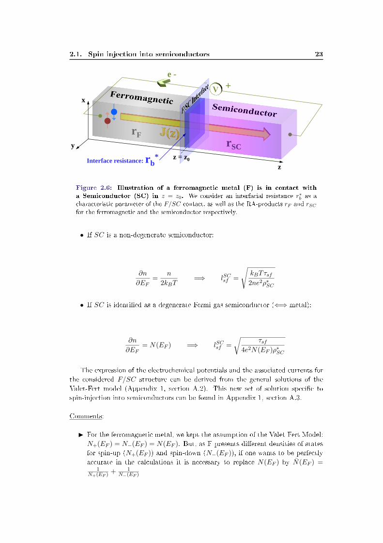
a Semiconductor (SC) in z = z0. We consider an interfacial resistance r∗b as a
characteristic parameter of the F/SC contact, as well as the RA-products rF and rSCfor the ferromagnetic and the semiconductor respectively.
• If SC is a non-degenerate semiconductor:
∂n
∂EF=
n
2kBT=⇒ lSCsf =
√kBTτsf2ne2ρ∗SC
• If SC is identied as a degenerate Fermi gas semiconductor (⇐⇒ metal):
∂n
∂EF= N(EF ) =⇒ lSCsf =
√τsf
4e2N(EF )ρ∗SC
The expression of the electrochemical potentials and the associated currents forthe considered F/SC structure can be derived from the general solutions of theValet-Fert model (Appendix 1, section A.2). This new set of solution specic tospin-injection into semiconductors can be found in Appendix 1, section A.3.
Comments:
I For the ferromagnetic metal, we kept the assumption of the Valet-Fert Model:N+(EF ) = N−(EF ) = N(EF ). But, as F presents dierent densities of statesfor spin-up (N+(EF )) and spin-down (N−(EF )), if one wants to be perfectlyaccurate in the calculations it is necessary to replace N(EF ) by N(EF ) =
1N+(EF ) + 1
N−(EF )

24Chapter 2. Conversion of a magnetic information into light
polarization information using spin-injected III-V semiconductors
Impact of the interface resistance on spin injection:In order to pull the blinds on the physics mechanisms ruling the spin injection
in semiconductors, it is interesting to pay close attention to the variation of currentspin polarization at the F/SC boundary: P bS . Using the expressions of the electro-chemical potentials and the associated currents for the considered F/SC structure(Appendix 1, section A.3), P bS can be expressed as a function of the interface re-sistance r∗b and the spin-RA products rF and rSC of the ferromagnetic and thesemiconductor respectively:
P bS =
(J+ − J−
J
)b
=βrF + γr∗b
rF + rSC + r∗b(2.18)
We use this expression of the current spin-polarization at the F/SC boundaryto discriminate dierent situations depending on the presence or not of interfaceresistance between F and SC. We also need to consider the relative ratio betweenr∗b and the spin-RA products (rF , rSC).
A) If there is no interface resistance: r∗b = 0:
The variations of current spin-polarization reduces to:
P bS =βrF
rF + rSC=
β
1 + rSCrF
As previously discussed, the expression of the spin diusion length and so rSCdepends on the semiconductor regime. Thus, we can distinguish two sub-cases:
1. r∗b = 0 and SC is a non-degenerate semiconductor:
We already dened in (2.13) that rF = ρ∗F × lFsf and rSC = ρ∗SC× lSCsf . Asin the Drude model (diusive regime) ρ = m
ne2τand using the expression
of lsf extracted from (2.29), it is possible to express the Spin-RA productsas a function of the carrier densities nF and nSC in the materials:
rF =
hπ
(3π2)16 e2
√τSCsf2τ
n− 2
3SC
rSC =
√2mkbT
τFsfτe2n−1
F
2.1. Spin injection into semiconductors 25
Despite the dierence of τsf values between the ferromagnetic metal andthe semiconductor (τFsf ≈ 1 ns << τSCsf ≈ 100 ns [75, 76]), the behaviorof rF and rSC is driven by the evolution of the carrier density n. Asthe semiconductor is non-degenerated, we can arm that nF >> nSCdirectly implying: rF << rSC . This means:
limrF<<rSC
r∗b=0
(P bS =
β
1 + rSCrF
)7−→ 0
We understand here the weak spin injection rates witnessed during therst spin injection experiments in semiconductors. This strong reductionof injected spin polarization had already been pointed out by Schimdt etal. [72]
2. r∗b = 0 and SC is identify as a degenerate Fermi gas semiconduc-
tor (⇐⇒ metal):
In this case nF ≈ nSC =⇒ rF ≈ rSC and:
limrF≈rSCr∗b=0
(P bS =
β
1 + rSCrF
)7−→ β
2
The spin polarization of the current penetrating the semiconductor isreduced by half from the value of the ferromagnetic bulk spin asymme-try coecient β. This situation holds when a ferromagnetic metal is incontact with a non-magnetic metal (Valet-Fert F/N case) such as theCo/Cu system for instance.
B) When an interface resistance is introduced: r∗b 6= 0:
Even in the presence of an interface resistance, the spin polarization injectedin the semiconductor will be signicant only if the spin dependent interfaceresistance is at least of the order of magnitude of the semiconductor resistance:r∗b ≥ rF , rSC.
1. If the interface resistance is high enough to fully control the
injection at interface: r∗b >> rF , rSC
It is not of importance here to separate the two cases of the degener-ate (rF ≈ rSC) and non-degenerate (rF << rSC) semiconductor becausefor both situations the interface resistance controls the behavior of thespin-injection. We have:

26Chapter 2. Conversion of a magnetic information into light
polarization information using spin-injected III-V semiconductors
limr∗b>>rF ,rSC
r∗b6=0
(P bS =
βrF + γr∗brF + rSC + r∗b
)7−→
γr∗br∗b
= γ
When the interface resistance drives the injection at the interface andfully overcome the impedance mismatch, the current spin polarization isgiven by the interfacial spin asymmetry γ.
2. If SC is non degenerated and r∗b ≈ rSC > rF :
limr∗b≈rSC>rF
r∗b6=0
(P bS
)7−→ γ
2
In practice, this intermediate regime is quite representative of ferromag-netic contacts on semiconductors. The spin accumulation is limited bythe spin relaxation in F (spin back-ow) induced by the coupling with theferromagnetic metal. Although it is still a manifestation of the impedancemismatch, it is usually classied as the "Back ow regime".
3. If SC is identify as a degenerate Fermi gas semiconductor (⇐⇒metal) and r∗b ≈ rSC ≈ rF :
limr∗b≈rSC≈rF
r∗b6=0
(P bS
)7−→ β + γ
3
The spin polarized current injected in the degenerate semiconductor hasa double dependance on the spin asymmetry occurring in the bulk of theferromagnetic injector and at the interface.

2.1. Spin injection into semiconductors 27
Conclusions: Theoretical conditions for an ecient experimentalspin injection in semiconductors:
As a rst thought, I would like to thanks and congratulate the reader for fol-lowing me through this bestiary of 18 equations in the name of the spin injectionunderstandings. Beyond all this mathematical formalism, the one fundamental con-cept to remember here for the successful implementation of a spin-optoelectronicdevice is that: a spin-dependent interface resistance r∗b , greater than the thresholdvalue rSC , needs to be inserted between the ferromagnetic metal spin injector andthe semiconductor.
In the absence of interface resistance, the Fermi energy splitting due to spin ac-cumulation ∆µ has the same value ∆µb on both side of the interface. When onegoes away from the interface, this spin accumulation decreases exponentially withdecays lengths lFsf and lSCsf . The variations of current spin polarization in F andSC are proportional to the respective spin-ip probabilities in F and SC. It isdemonstrable that with the same ∆µb in F and SC these total spin-ip rates arerespectively proportional to 1
rFand 1
rSC. When the semiconductor is non-degenerate
rF << rSC , the spin-ip rate and so the spin-depolarization of the current are moreimportant in F than in SC. To summarize, without interface resistance (r∗b = 0), thecurrent is already completely depolarized when it crosses the interface (P bS 7−→ 0).The addition of an interface resistance introduces a spin dependent discontinuity of∆µ at the interface and generate a much higher ∆µ in the semiconductor than in theferromagnetic metal. This leads to a more balanced spin-ip ratio between F andSC thus restoring the spin polarization at the interface and in the semiconductor.
The resistance and the depolarization at an interface can be measured experimen-tally [77]. Most of the time in the literature, the F/SC junctions are characterizedby the tension variation ∆V associated with their Resistance-Area (RA) productindependent of the junction dimensions:
RSA =∆V
IA =
γ∆µ
2eJ= γrSC
(βrF + γr∗b
rF + rSC + r∗b
)7−→
rF<<rSC ,r∗bγ2r∗brSCr∗b + rSC
(2.19)
Ideally, from the experimental perspective, one wants to prepare a system thatts the case B)1). The very high resistance required by the condition rSC << r∗bcombines with the need of a signicant spin asymmetry γ can be delivered by tun-nel junctions. These Magnetic-Tunnel-Junction (MTJ) are achieved by insertingan ultra-thin insulating layer between the ferromagnetic metal and the semiconduc-tor. Because of the excellent results they display in metallic systems, the two mostused barrier materials are the aluminum oxide (AlOx) and the magnesium oxide(MgO) [100, 103, 99, 97].Another way is to use Schottky barriers by putting the ferromagnetic injector di-rectly in contact with the semiconductor over-doped on a small thickness at the

28Chapter 2. Conversion of a magnetic information into light
polarization information using spin-injected III-V semiconductors
-400n -200n 0 200n 400n 600n 800n 1µ
0.0%
0.1%
0.2%
0.3%
0.4%
0.5%SCF
Cu
rren
t P
ola
riza
tion
(%
)
Position z (nm)
rb
*=0
rb
*=r
SC=4.10
3.m
2
=0,46
=0,5
lsf
SC=1,2m
lsf
F=60nm
0.01 0.1 1 10 100
0.0
0.2
0.4
0.6
0.8
1.0
PS
b/
rb
*/r
SC
PS
b /
a) b)
Figure 2.7: (a) Evolution of the current spin polarization at a Ferromag-
netic/Semiconductor interface for dierent values interface resistance. We
considered the case where the interface resistance is non-existant (blue) and the case
where the interface resistance is of the order-of-magnitude of the semiconductor resis-
tance (red). (b) Evolution of the normalized current spin polarization at the
interface as a function of the ratio between the interface resistance and the semicon-
ductor resistance. Figure adapted from [67].
interface. The spin-polarized electrons are injected by tunnel eect through the po-tential barrier created by the Schottky contact. These Schottky injectors also displaylarge interface resistances but it requires most of the time an important band engi-neering development to control the height and the thickness of the potential barrierin order to get an ecient electrons tunneling.
The reader should be aware that, despite the fundamental understandings it pro-vides, the above-introduced study remains a simplied approach of spin-injectioninto semiconductors. The reality tends to be more complex as the nature of theF/SC or F/T/SC contacts modies the pinning of the Fermi level in the bandstructure. Such structure and interfaces can also tune the carrier population andtrigger electric eld variations near the interface(s).
In the next section, we will walk through the dierent ways to generate a spin-polarized current in a semiconductor structure. In terms of direct injection, as theygave and still give the most impressive results in the literature, we will pay a particu-lar attention to the MTJ and Schottky barrier injectors. We can already reveal thatwe are also working with MTJ spin-injectors based on MgO/CoFeB/Ta multilay-ers for our experiments with Spin-LED and Spin-VECSEL. Their optimization andthe experimental results they provided during this Ph.D will be precisely detailedin the third chapter of the manuscript.

2.1. Spin injection into semiconductors 29
2.1.2 Generation of a spin-polarized carriers in a semiconductor
When it comes to generating a spin-current in a semiconductor, several methodscan be explored. Obviously, what rst comes to mind is the use of a ferromagneticmaterials directly in contact with the semiconductor to be used as a spin-polarizer.But, in well designed devices, one has also the possibility to take advantages ofsome physical mechanisms link to light/matter interaction, heat diusion or whetherelectronic diusion to indirectly engender a spin accumulation. This second sectionis fully devoted to the introduction and the description of these state-of-the-artmechanisms.
Figure 2.8: Illustration of three physical mechanism generator of spin imbalance in
a non-magnetic material. Figure reprinted from [78].
2.1.2.1 Electrical spin-injection from a ferromagnetic metals
Here we discuss the generation of a spin polarized current in a semiconductor using"direct spin-injection" through ferromagnetic metals. The generation of a spin-current, in the two-spin channels conduction model, is directly associated with adisequilibrium between the spin-up electrons and the spin-down electrons popula-tions. It is useful to emphasize the important distinction between the spin polariza-tion of the injected electron current and the spin polarization of the electron density.Indeed, even if an injected current is highly polarized, it can result in small changesin the spin population of conduction electrons if the electron gas into which theinjection occurs has a high density or if the injection current magnitude is small [79].
The use of ferromagnetic metals as spin-injector on non-magnetic metallic and semi-conductors structures was rst theoretically predicted by Aronov & Pikus in 1976.Their research were stimulated by the early work of Tedrow & Meservey on spininjection in superconductors using Ferromagnetic (F)/Insulator (I)/Superconductor(S) junctions [80]. In 1971, they succeeded in measuring the spin polarization at theFM/I interface using Andreev reexion experiment.3
3The Andreev reection (Andreev 1964) is a scattering process responsible for a conversion
between a dissipative quasi-particle current and a dissipation-less super-current.

30Chapter 2. Conversion of a magnetic information into light
polarization information using spin-injected III-V semiconductors
Non-Magnetic Ferromagnetic Half-Metallic
E E E
EF EF EF
n↑ n↑ n↑
n↓ n↓
n↓
3d↑ Band-Splitting
PS = 0% 0%< PS < 100% PS = 100%
n↑ = n↓ n↑ > n↓ n↓ = 0
3d↑ 3d↑ 3d↓
3d↓
3d↓
Figure 2.9: Scheme of the 3d-band structures for a non-magnetic metal, a
ferromagnetic metal and a Half-Metal. It illustrates how the spin-polarization
PS directly depends on the dierence of DOS for the two spin populations at the Fermi
level generated by the spin-splitting of the d-states
The use of ferromagnetic metals (Fe, Co, Ni) and their alloys (CoFe, CoFeB,NiFe) for spin-injection experiments is motivated by their high Curie temperatureTc. This property makes them particularly suitable for room temperature applica-tions and potential future spintronics devices (Table 2.1). In a ferromagnetic metal,the DOS at the Fermi level has both s- and d- components. The exchange interactionin the ferromagnet leads to a spin-splitting of the d-states and therefore to dierentDOS for the two spin populations at the Fermi level (Figure 2.9) [81]. The currentowing in the metal is carried by the s-electrons since s-electrons have signicantlysmaller eective mass compared to d-electrons. However, due to the splitting of thed-like DOS, spin-up and spin-down electrons have dierent probabilities of scatter-ing into the d-states. This result in dierent mobilities for spin-up and spin-downs-electrons [82]. Consequently, the current ow will be dominated by s-electrons inthe spin-state with the less d-like DOS at the Fermi level. The spin polarization ofthe ferromagnetic at the Fermi level is given by:
PFS =nF↑ − nF↓nF↑ + nF↓
(2.20)
where nF↑ and nF↓ are the DOS at the Fermi level for spin-up and spin-down inthe ferromagnet respectively. It describes the degree to which one spin sub-bandis occupied relative to the other. Experimental values of spin-polarization for com-monly used ferromagnetic metals and alloys are given in Table 2.1 [83]4.
4These experimental results were measured using Ferromagnetic/Al2O3/Superconductor tun-

2.1. Spin injection into semiconductors 31
PS M Bs Hc µmax Tc ρ
Metal % 103kg ·m−3 T A ·m−1 - K 10−8Ω ·m
Fe 44 7.8 2.15 4 180000 1043 10
Co 45 8.9 1.79 1600 - 1400 6.24
Ni 33 8.9 0.615 800 1000 631 6.84
Co50Fe50 51 - - - - 1388 -
Ni80Fe20 48 - 0.75 - 300000 723 -
Table 2.1: Intrinsic spin polarization and datasheet of the ferromagnetic metals and
alloys commonly used as spin-injectors
The spin-polarization of the current injected into the non-magnetic semiconduc-tor PSCS is typically used to characterize the spin injection eciency of the ferro-magnet/semiconductor structure. The injected spin-polarization and spin-injectioneciency η are dened as [84]:
PSCS =
nSC↑ − nSC↓nSC↑ + nSC↓
η =PSCSPFS
(2.21)
where nSC↑ and nSC↓ represent the DOS at the Fermi level for majority and mi-nority spins in the non-magnetic semiconductor respectively. While the choice ofPFS requires careful considerations [85, 86], η provides a gure of merit for the com-parison of various spin injection structures. To this day, the spin injection eciencyis experimentally always inferior to 100% due to limitations factors such as interfacequality, defect/impurity densities, band structures but also by the limited intrinsicspin polarization of ferromagnet PFS (up to 50% for the best ferromagnetic met-als). Studies revealed that interface defects such as stacking faults, poorly matchedband symmetries and the formation of "magnetically dead" interfacial layers duringepitaxial growth all result in reduced spin injection eciencies [84, 87].
As introduced in the previous section, with a normal ohmic contact betweena ferromagnetic and a semiconductor, the large conductivity mismatch [72] leadsto nearly negligible spin injection eciency. The interfacial resistance r∗b necessaryto reach an ecient spin injection regime can be experimentally implemented bythe use of a tunnel contact. There are dierent ways to implement a tunnel bar-rier in semiconductors. Theoretically, Fermi electrons cannot enter the conductionband of most semiconductors from a metallic contact without undergoing a tun-neling through the native Schottky barrier [88]. An ecient tunnel contact can be
nel junctions. The values of the conduction electrons spin-polarization PS depend of the measure-
ment technique.
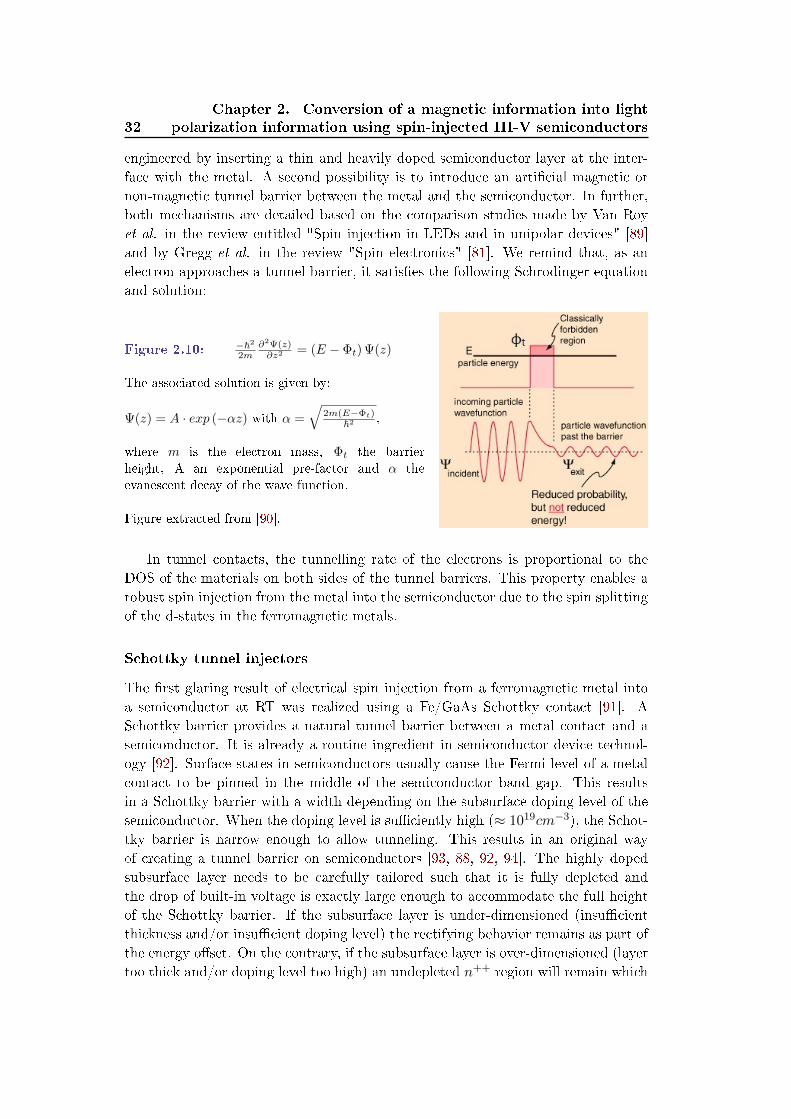
32Chapter 2. Conversion of a magnetic information into light
polarization information using spin-injected III-V semiconductors
engineered by inserting a thin and heavily doped semiconductor layer at the inter-face with the metal. A second possibility is to introduce an articial magnetic ornon-magnetic tunnel barrier between the metal and the semiconductor. In further,both mechanisms are detailed based on the comparison studies made by Van Royet al. in the review entitled "Spin injection in LEDs and in unipolar devices" [89]and by Gregg et al. in the review "Spin electronics" [81]. We remind that, as anelectron approaches a tunnel barrier, it satises the following Schrodinger equationand solution:
Figure 2.10: −~2
2m∂2Ψ(z)∂z2 = (E − Φt) Ψ(z)
The associated solution is given by:
Ψ(z) = A · exp (−αz) with α =√
2m(E−Φt)~2 ,
where m is the electron mass, Φt the barrier
height, A an exponential pre-factor and α the
evanescent decay of the wave function.
Figure extracted from [90].
In tunnel contacts, the tunnelling rate of the electrons is proportional to theDOS of the materials on both sides of the tunnel barriers. This property enables arobust spin injection from the metal into the semiconductor due to the spin splittingof the d-states in the ferromagnetic metals.
Schottky tunnel injectors
The rst glaring result of electrical spin injection from a ferromagnetic metal intoa semiconductor at RT was realized using a Fe/GaAs Schottky contact [91]. ASchottky barrier provides a natural tunnel barrier between a metal contact and asemiconductor. It is already a routine ingredient in semiconductor device technol-ogy [92]. Surface states in semiconductors usually cause the Fermi level of a metalcontact to be pinned in the middle of the semiconductor band gap. This resultsin a Schottky barrier with a width depending on the subsurface doping level of thesemiconductor. When the doping level is suciently high (≈ 1019cm−3), the Schot-tky barrier is narrow enough to allow tunneling. This results in an original wayof creating a tunnel barrier on semiconductors [93, 88, 92, 94]. The highly dopedsubsurface layer needs to be carefully tailored such that it is fully depleted andthe drop of built-in voltage is exactly large enough to accommodate the full heightof the Schottky barrier. If the subsurface layer is under-dimensioned (insucientthickness and/or insucient doping level) the rectifying behavior remains as part ofthe energy oset. On the contrary, if the subsurface layer is over-dimensioned (layertoo thick and/or doping level too high) an undepleted n++ region will remain which
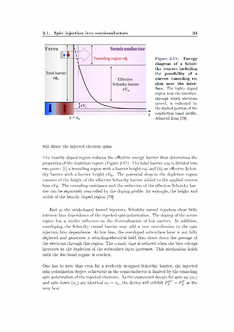
2.1. Spin injection into semiconductors 33
Total barrier
eφb
Tunneling region eφt
Effective
Schottky barrier
eVbi
eVr
Ferro Semiconductor
z = z0 z
e- e-
Figure 2.11: Energy
diagram of a Schot-
tky contact including
the possibility of a
narrow tunneling re-
gion near the inter-
face. The highly doped
region near the interface,
through which electrons
tunnel, is indicated by
the dashed portion of the
conduction band prole.
Adapted from [79].
will dilute the injected electron spins.
The heavily doped region reduces the eective energy barrier that determines theproperties of the depletion region (Figure 2.11). The total barrier eφb is divided intotwo parts: (i) a tunneling region with a barrier height eφt and (ii) an eective Schot-tky barrier with a barrier height eVbi. The potential drop in the depletion regionconsists of the height of the eective Schottky barrier added to the applied reversebias eVR. The tunneling resistance and the reduction of the eective Schottky bar-rier can be separately controlled by the doping prole: for example, the height andwidth of the heavily doped region [79].
Just as the oxide-based tunnel injectors, Schottky tunnel injectors show littleintrinsic bias dependence of the injected spin-polarization. The doping of the activeregion has a similar inuence on the thermalization of hot carriers. In addition,overdoping the Schottky tunnel barrier may add a new contribution to the spininjection bias dependence. At low bias, the overdoped subsurface layer is not fullydepleted and generates a retarding-electrical eld that slows down the passage ofthe electrons through this region. The transit time is reduced when the bias voltageincreases as the depletion of the subsurface layer increases. This mechanism holdsuntil the at-band regime is reached.
One has to note that even for a perfectly designed Schottky barrier, the injectedspin polarization degree achievable in the semiconductor is limited by the tunnelingspin polarization of the injected electrons. As the evanescent decays for spin up (α↑)and spin down (α↓) are identical α↑ = α↓, the device will exhibit PSCS = PFS at thevery best.
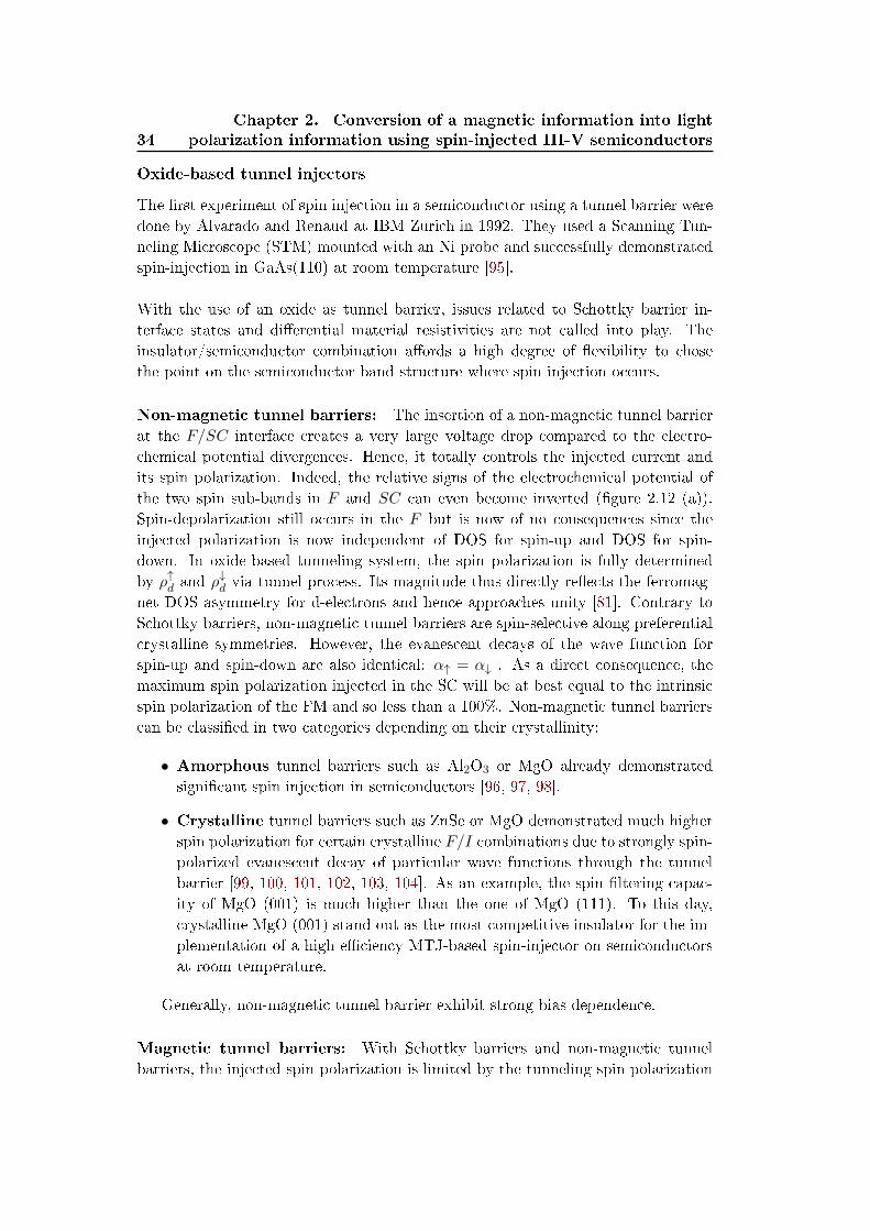
34Chapter 2. Conversion of a magnetic information into light
polarization information using spin-injected III-V semiconductors
Oxide-based tunnel injectors
The rst experiment of spin injection in a semiconductor using a tunnel barrier weredone by Alvarado and Renaud at IBM Zurich in 1992. They used a Scanning Tun-neling Microscope (STM) mounted with an Ni probe and successfully demonstratedspin-injection in GaAs(110) at room temperature [95].
With the use of an oxide as tunnel barrier, issues related to Schottky barrier in-terface states and dierential material resistivities are not called into play. Theinsulator/semiconductor combination aords a high degree of exibility to chosethe point on the semiconductor band structure where spin injection occurs.
Non-magnetic tunnel barriers: The insertion of a non-magnetic tunnel barrierat the F/SC interface creates a very large voltage drop compared to the electro-chemical potential divergences. Hence, it totally controls the injected current andits spin polarization. Indeed, the relative signs of the electrochemical potential ofthe two spin sub-bands in F and SC can even become inverted (gure 2.12 (a)).Spin-depolarization still occurs in the F but is now of no consequences since theinjected polarization is now independent of DOS for spin-up and DOS for spin-down. In oxide-based tunneling system, the spin polarization is fully determinedby ρ↑d and ρ
↓d via tunnel process. Its magnitude thus directly reects the ferromag-
net DOS asymmetry for d-electrons and hence approaches unity [81]. Contrary toSchottky barriers, non-magnetic tunnel barriers are spin-selective along preferentialcrystalline symmetries. However, the evanescent decays of the wave function forspin-up and spin-down are also identical: α↑ = α↓ . As a direct consequence, themaximum spin polarization injected in the SC will be at best equal to the intrinsicspin polarization of the FM and so less than a 100%. Non-magnetic tunnel barrierscan be classied in two categories depending on their crystallinity:
• Amorphous tunnel barriers such as Al2O3 or MgO already demonstratedsignicant spin injection in semiconductors [96, 97, 98].
• Crystalline tunnel barriers such as ZnSe or MgO demonstrated much higherspin polarization for certain crystalline F/I combinations due to strongly spin-polarized evanescent decay of particular wave functions through the tunnelbarrier [99, 100, 101, 102, 103, 104]. As an example, the spin ltering capac-ity of MgO (001) is much higher than the one of MgO (111). To this day,crystalline MgO (001) stand out as the most competitive insulator for the im-plementation of a high eciency MTJ-based spin-injector on semiconductorsat room temperature.
Generally, non-magnetic tunnel barrier exhibit strong bias dependence.
Magnetic tunnel barriers: With Schottky barriers and non-magnetic tunnelbarriers, the injected spin polarization is limited by the tunneling spin polarization

2.1. Spin injection into semiconductors 35
Spin-split
Insulator
N-doped
semiconductor
Conduction
band
Valence
band
Metal
(a) (b)
Figure 2.12: (a) Evolution of the electrochemical potentials at an interface F/I/SC.
(b) Unbiased spin-split insulator band structure. Figures reprinted from [81].
of the injected electrons (α↑ = α↓). The alternative solution to theoretically ap-proach an injected spin polarization of 100% is to perform tunnel injection froma ferromagnetic metal into a semiconductor through a spin-split magnetic insula-tor (gure 2.12 (b)). Contrary to non-magnetic insulator, the spin-ltering eectis driven by the spin splitting of the insulator bandgap. Consequently, a tunnel-ing electron with its energy in the bandgap sees dierent heights of tunnel barrierdepending on its spin. The band splitting of insulator means that the two spin chan-nels exhibit dierent evanescent decay rates. The injected spin polarization into thesemiconductor is then given as PSCS = 1− exp(t∆α) where t is the barrier thickness
and ∆α is the dierence in decay rates α↑ − α↓ with α↑,↓ =
√2m(E↑,↓)
~2 [81]. Forincident electrons already signicantly spin-polarized, this leads to reinforcement ofthe spin asymmetry for the tunnel current with a potential spin-injection polariza-tion in the SC higher than the intrinsic spin-polarization of the F . Therefore, bypotentially enhancing the spin injection and exhibiting a weaker bias dependance,spin-split magnetic insulators such as EuO stand out as interesting candidates forthe realization of high eciency MTJ spin-injectors.
Schottky vs. Oxide-based Tunnel Injectors
For electrical spin injection, beyond the properties of the chosen tunnel barriers(Schottky, non-magnetic oxide or magnetic oxide), interfaces qualities and proper-ties have been shown to be of critical importance in spin-dependent tunnel experi-ments [105, 106]. Hence, the value of the injected spin polarization reached in thesemiconductor does not only depends on the materials choice but also and mainlyon the materials crystalline qualities (MBE vs. Sputtering), the lattice mismatchesand the matching of the materials band structures.

36Chapter 2. Conversion of a magnetic information into light
polarization information using spin-injected III-V semiconductors
In term of growth method and in contrast with the oxide tunnel barriers, the ferro-magnetic Schottky contact needs to be deposited in-situ since oxidation of the toppart would damage the careful design of the n++ doped layer. In-situ depositionon a crystalline semiconductor surface has the advantage to allow the growth ofepitaxial, single crystalline, magnetic contacts. It provides a control over the mag-netic properties than layers deposited on amorphous oxide such as AlOx or MgO.Experiments showed that epitaxial Fe contacts result in injected spin polarizationsthat are very similar to those obtained with Fe/AlOx and CoFeB/AlOx spin in-jectors [107]. Generally, tunneling through reverse-biased Schottky diodes formedwith ferromagnetic metals have been experimentally proven to result in high spin-injection eciencies [92].
Also, a comparative study between a F/SC Schottky tunnel junction and F/Al2O3/SCnon-magnetic oxide-based tunnel junction grown on LED showed a higher operatingeciency by a factor of 10 for the Schottky barrier. This dierence was attributedto a combination of factors linked to the higher surface recombination velocities inthe case of the oxide barrier, the scattering at the Al2O3/SC interface and/or dif-ferences in tunnel electron energies [107].
On the other hand, the use of an oxide tunnel barrier prevents any intermixingof the ferromagnetic metal and the semiconductor. Thus, this type a barrier leadsto a much better thermal stability compared to the Schottky barriers [108]. Gen-erally, the introduction of an oxide layer allows the fabrication of more stable androbust spin-injectors.
Using a Spin-LED conguration5, typical injected spin-polarization degree measuredwith Schottky tunnel barriers are around 30%, but only at low temperatures [92].Typical values reached with AlOx barriers on GaAs are around 25-40% at low tem-perature (4.2 - 77 K) [109, 98, 107] and up to 16% at 300 K while with epitaxialMgO(001)/CoFeB on GaAs spin polarization degrees up to 52% at 100 K [100, 101]and 32% at 300 K [99] are obtained. The highest spin-selectivity of the epitaxialMgO(001)/CoFeB lead to an increase of the spin-injection eciency.
Conclusion: Choice of electrical spin-injector
We can conclude from this analysis and the state-of-the-art experimental work thatthe most attractive multilayer structure to eciently spin-inject a semiconductor atroom temperature is a Magnetic-Tunnel-Junction based on the combination of: 1)the high intrinsic spin-polarization ferromagnetic metal: CoFeB with 2) the crys-talline MgO(001) tunnel barrier. Additionally, under careful structural engineering,a MgO(001)/CoFeB/Ta MTJ oers the possibility to display Perpendicular Mag-
5For more informations, injectors eciency comparisons and detection geometries in Spin-LED
systems, please refer to the comparison table in section 2.2.2.2: State-of-the-Art

2.1. Spin injection into semiconductors 37
netic Anisotropy at room temperature. This colossal advantage over Schottky bar-rier injectors motivated the important optimization work achieved during this Ph.Don MgO(001)/CoFeB/Ta injectors using Spin-LEDs to ideally reach device operationwith Perpendicular Magnetic remanence at room temperature. The combination ofthe Ta capping with a Rapid Thermal Annealing (RTA) (≈ 250C during 3 minuts)leads to a re-crystallization of the amorphous CoFeB layer thanks to the pumpingof B by the Ta layer and the restructuration of the CoFe from the interface with thecrystalline MgO(001).
Beyond these standard methods inherited from spintronics with metal systems, itis interesting to mention that other type of injectors oers really attractive spin-injection performances:
• Diluted Magnetic Semiconductors: Magnetic semiconductors were therst successful sources for spin injection into a non-magnetic semiconductor.By combining two domains of condensed matter physics: semiconductors andmagnetism, they generated a strong interest. A DMS is built on two dis-tinct elements: a semiconductive matrix where magnetic impurities are intro-duced. The spin exchange interaction between the magnetic impurities (andso the macroscopic behavior of the DMS magnetization) depends on the semi-conductive matrix surrounding the impurities as well as their nature, spatialdistribution and concentration. The percentage of incorporated magnetic im-purities is relatively low, usually less than 10%. All these parameters makethe growth of a DMS quite challenging. To this day, the international commu-nity deployed a special eort on the study of III-V based DMS and especially(Ga,Mn)As [110, 111, 112, 113]. It was shown that with an optimized dopingdesign and high-quality (Ga,Mn)As lms, injected electron spin polarizationsof 80% at 4.2 K and 25% at 80 K can be achieved [89, 113, 84]6.
• Half-Metallic Ferromagnets: In the ideal limit where only one spin di-rection remains at the Fermi level, the spin polarization of the conductionelectrons is maximal: PS = 100%. The materials exhibiting this unique prop-erty are named Half-metals. A half-metallic ferromagnet (HMF) behaves likea metal for one spin direction and like an insulator for the other spin direc-tion [115, 116, 117, 115, 118]. Generally, half-metallic compounds stand outas really attractive candidates to play the role of high spin-polarized currentsources to perform spin injection into semiconductors. They come out as apotential solution to overcome the intrinsic spin polarization limitation at theFermi level of common transition metals Fe, Co, Ni (PS ≈ 30 to 40%) createdby the s-d band hybridization. The spin-ip loss is canceled by the completeabsence of nal states for spin ipping.Nevertheless, so far only pioneering investigations have been conducted on the
6For complementary information on Diluted Magnetic Semiconductors, please refer to refer-
ence [114]

38Chapter 2. Conversion of a magnetic information into light
polarization information using spin-injected III-V semiconductors
growth of Heusler HMF/SC hybrid structures [119, 120, 121, 122]. The high-est injected spin-polarization degree reached was around 13% at 5 K using o-stoichiometric Co1.6Mn2.4Ga on InGaAs [121]. An injected spin polarizationof 27% at 2K was reported for the system Co2MnGe/GaAs [123], contrastingwith the value of 40% reached with a standard Fe injectors. Since spin injec-tion experiments probe the spin polarization at the interface, a realistic theorydoes not only need to consider the electronic structure of the interface, butalso the presence of atomic disorder as well as the eects of non-zero tempera-ture. Indeed, these factors play an essential role in interpreting spin injectionmeasurements on new materials [117]. From a pragmatic view point, as theinterface is controlling the spin injection, the real challenge is to develop ahalf-metallic interface.In terms of realistic application for spin-injection, the hunt for a half-metallicferromagnet exhibiting a high TC , a control of the atomic disorder and a con-trol of the interface structure is still on7.
2.1.2.2 Generation of spin accumulation: Beyond direct spin injection
We highlighted that the impedance mismatch issue at a F/SC interface arises fromthe injection of a spin polarized current across the interface between two materialswith highly dierent conductivities. Thus, it seems reasonable to consider that thisproblem vanishes if spins are injected into the semiconductor using pure spin currentwithout charge transport [124].
In recent years, new sources of pure spin currents have been demonstrated [125, 126,127, 128] and applied [7, 8, 25]. A pure spin current correspond to the transportof spin angular momentum without net charge currents. In this section we presentstate-of-the-art methods for generating pure spin current in semiconductors.
Spin-Hall Eect and Inverse Spin-Hall Eect
The Spin Hall Eect was predicted in 1971 [129] and stands for a collection ofphenomena resulting from spin-orbit coupling. An electrical current owing througha sample can lead to spin transport in a perpendicular direction as well as a spinaccumulation at lateral boundaries [130]. These purely electrical mechanisms donot require applied magnetic eld nor feromagnets and are consequently application"friendly". These eects can be observed in materials with strong Spin-Orbit (SO)as the SO coupling acts like an eective magnetic eld HSO on the spin of themoving electrons.
The Spin-Hall Eect: The spin-hall eect (SHE) originates from the spin-orbitinteraction (SOI) that couples the electron spin to the orbital motion of the elec-
7For complementary information on Half-Metallic Ferromagnets and Heusler Alloys, please refer
to reference [117]

2.1. Spin injection into semiconductors 39
Figure 2.13: (a) Schematic mechanism of the Spin Hall Eect converting
a charge current into a spin current. (b) Schematic mechanism of the Inverse
Spin Hall Eect, reciprocal mechanism converting a pure spin current into a charge
current. Figure reprinted from [130].
tron [131]. The origin of the SHE is classied as: (i) intrinsic if SO eects on thewave functions of conduction band are predominant or (ii) extrinsic if SO eectsoccur on the scattering potential of impurities or defects. In a non-magnetic con-ductor the SOI generates a pure spin current Jspin orthogonal to the charge currentJcharge (Figure 2.13 (a)). If the lateral dimension of the sample is larger than thespin diusion length, a spin accumulation is induced on the edges of the sample andcan directly be measured electrically [132, 133, 130]. The rst observation of SHE insemiconductors was detected and imaged with the use of Kerr rotation microscopyin 2004 by Kato et al. [134].
The conversion eciency of the charge current density into spin current densityis characterized by the Spin Hall Angle (SHA) given by:
θSHE =JspinJcharge
(2.22)
where Jspin and Jcharge are the pure spin current and the charge current re-spectively. Promising application could be foreseen if the conversion eciency ofcharge current into spin current becomes competitive with the values reached usingF/N interfaces [135]. The use of SHE lead to the developpement of experimentsand concept involving the spin-torque switching of ferro-magnets [136], spin-torqueferromagnetic resonance [137] and the SHE-Transistors [138].
The Inverse Spin-Hall Eect: The Inverse Spin-Hall Eect (ISHE) qualiesthe SHE reciprocal mechanism in which a pure spin current can be converted intoa charge current and a charge accumulation. The ISHE is caused by the bending ofelectron orbits of up and down spins into opposite directions normal to their groupvelocity, owing to the spin-orbit interaction [139, 140, 126, 141] (Figure 2.13 (b)). It

40Chapter 2. Conversion of a magnetic information into light
polarization information using spin-injected III-V semiconductors
generates relatively large voltage for heavy metals such as Pt and has the advantageto scale linearly with the device lentgh.
Spin-Caloritronics
The new-born research eld of Spin-Caloritronics focuses on non-equilibrium phe-nomena related to spin, charge and heat transport in magnetic structures and de-vices [139, 142]. This recently invigorated eld is of high interest for creating spin-currents and pure spin-currents in systems hosting important temperature gradient.The Spin Seebeck Eect (SSE) is observed when a thermal gradient applied to aspin-polarized material in conact with a non spin-polarized material. It leads to aspatially varying transverse spin current in an adjacent non-spin-polarized material.Then, this spin-current usualy gets converted into a measurable voltage using ISHE(Figure 2.14 (a)) [143]. Its eciency is characterized by the spin Seebeck coecientS = (σ↑S↑ + σ↓S↓) / (σ↑ + σ↓). It corresponds to the ratio of measured voltage perunit of length to the temperature gradient. In a metallic magnet spin-↑ and spin-↓ conduction electrons notably have have dierent scattering rates and densities.It directly implyes that the two spin channels have dierent Seebeck coecients(S↑ 6= S↓) [144]. When a temperature gradient is applied, a spin accumulationµ↑ − µ↓ proportional to the temperature dierence appears. Therefore, in the spinsector, a magnet works in the same way as a thermocouple [128]. In a ferromagnet,the SSE results from the interaction between phonons and magnons (excitations ofmagnetic moments), which creates a gradient in the magnetization across the sam-ple [145, 146, 147, 142, 148, 149, 150, 144]. The dissipation of angular momentumgenerates a spin current owing into the adjacent non-magnetic material. This ef-fect is interpreted in terms of a spin current injected into the non-magnetic materialfrom the ferromagnet [128]. The thermally induced spin voltage persists even atdistances far from the sample ends (several millimeters) and spins can be extractedfrom any position on the magnet by simply contacting a metal. The conversion ofthe pure spin-current generated by the thermal gradient into a measurable voltageocurs through Inverse-Spin-Hall-Eect (ISHE).
The Spin Seebeck Eect has been discovered rst in Ni81Fe19/Pt systems by Uchidaet al in 2008 [128] and later in other magnetically ordered materials such as theelectrically insulating Yttrium Iron Garnet (YIG = LaY2Fe5O12) [151], the DilutedMagnetic Semiconductor GaMnAs [19], Heusler alloys (Co2MnSi) [152] with a mag-nitude of microvolts per Kelvin. Lately, SSE has also been demonstrated in theintrinsically non-magnetic Te-doped n-type III-V semiconductors InSb [143]. TheSSE could be directly applicable to the construction of thermo-power generatorsto drive spintronics devices [153] or devices such as Spin Seebeck-assisted mag-netic random access memories [154]. Combined with the ISHE it could also leadto temperature gradient sensors as well as thermoelectric generators, allowing newapproaches towards the improvement of thermoelectric generation eciency. Nev-ertheless in terms of realistic applications, it remains to be seen whether a magnetic

2.1. Spin injection into semiconductors 41
(a)
Spin polarization induced by
Seebeck Spin Tunneling
(b)
Figure 2.14: (a) Transverse experimental conguration use for the obser-
vation of SSE: The system is composed of a ferromagnetic material subjected to a
temperature gradient ∇T in contact with a non-magnetic Pt wire orthogonal to ∇T .The whole system is placed in a large magnetic eld that has a direction parallel to
∇T . Owing to the large eld, more electrons have spins (black arrows) that align
parallel with the eld than antiparallel to it. This strong spin polarization and the
temperature gradient generates a pure spin current in the ferromagnet detected as a
voltage thanks to a Platinum (Pt) wire. The ISHE voltage generated can be amplied
by increasing the length of the Pt wire. Figure reprinted from [155]. (b) Basic con-
cept of Seebeck spin tunneling: In a tunnel contact between a F electrode and a
N electrode, a temperature dierence between the electrodes causes a transfer of spin
angular momentum from the F to N . The thermal spin current requires no tunnel
charge current. Figure reprinted from [156].
eld is needed at all to observe SSE at room temperature.Interestingly, ecient spin injection using Spin-Dependent Seebeck Eect (SDSE)
has recently been demonstrated in lateral F/N/F spin-valve structures [144]. Butalso in a dedicated perpendicular spin-valve nanostructure consisting of two ferro-magnetic layers (15 nm Ni80Fe20) separated by a non-ferromagnetic metal (15 nmCu) [157]. Amazingly, Le Breton et al. also reported the demonstration of SeebeckSpin Tunneling (SST) generated in a Ferromagnet-Oxide-Silicon tunnel junction(Figure 2.14 (b)) [156]. The mechanisms involved are dierent as the thermal spinow is of purely interfacial nature.
The SST stands out as a very interesting eect to use in optical experiments wheresignicant thermal gradient are usually engaged due to the use of lasers. A laserbeam well focused on the ferromagnet can be use to generate a temperature gradientin TMR junctions [158] or in a F/T/SC structures. It could trigger spin-injectionin the devices without the need for circularly polarized light and optical orienta-tion. The total spin-injection yield in the QWs of Spin-LEDs and Spin-VCSELscould then be optimized by assisting the injection of the conventional spin-polarizedcharge current with pure spin-currents generated by SST. For semiconductor lasersespecially, SST could be used to : (i) increase the global eciency of the systemby functionalizing the signicant heat losses and (ii) combine the pure spin current

42Chapter 2. Conversion of a magnetic information into light
polarization information using spin-injected III-V semiconductors
with the non-linear amplication eects of the optical cavity to control the lasermodes polarization. Fairly large SST eect has already been observed and carriesthe promise of useful applications.
Spin-Pumping and Ferromagnetic Resonance
In 2011, Ando et al. proposed with a new approach to overcome the impedencemismatch at a Ferromagnetic/Semiconductor interface: the Spin Pumping [124].Contrary to spin-injection by carrier transport through the F/SC interface, here apure spin current is injected in the SC by Ferromagnetic Resonnance (FMR) fromthe F layer (Figure 2.15 (a)) [127, 159, 160, 161].
(b) (a) (a) 1. 2.
Figure 2.15: (a) Comparison between spin injection through carrier trans-
port and dynamical exchange: 1. Scheme of the conventional electrical spin injec-
tion by carrier transport through the F/N interface 2. Scheme of the spin pumping
mechanism. A pure spin current is injected in the non-magnetic material by induced
Ferromagnetic Resonance of the F layer. Figure Reprinted from [124]. (b) Detection
conguration: the injected pure spin current is detected as a spin voltage on the
sample edges using ISHE.
The concept is based on the use of a F/N -bilayer placed in a radiofrequency eldin the GHz range. These microwaves engage a Ferromagnetic Resonnance (FMR)of the FM layer magnetization under a specic external magnetic eld. The mag-netization's precession associated with a change of the longitudinal component ofthe magnetization is transfered to the electronic bath at the F/N interface throughdynamical exchange interaction and generate a vertical pure spin current in thenon-magnetic metal. As for the Spin Seebeck Eect, the spin accumulation inducedby spin-pumping in the non-magnetic metal is detected as a voltage using ISHE(Figure 2.15 (b)). Additionally, the spin pumping can be tuned by applying a biasvoltage at the F/N interface and controlling the level exchange interaction.
Tunable spin injection from Ni81Fe19 into both p- and n-doped GaAs through bothOhmic and Schottky contacts has been demonstrated with an ISHE detection at

2.1. Spin injection into semiconductors 43
room temperature [124]. The spin pumping is a powerful and versatil method withpotential spin injection capability into a wide range of material free from the im-pedence mismatch issue. As it only requires a precession of the F layer magnetiza-tion, this method can be integrated on a wide range of systems such as spin-torqueoscillators or semiconductor spin-laser [162]. The spin-pumping is also a very prac-tical tool to characterize and measure the Spin Hall Angle in a material using theISHE [137, 163, 164, 165, 166].

44Chapter 2. Conversion of a magnetic information into light
polarization information using spin-injected III-V semiconductors
2.1.3 Spin-Orbit interaction and Spin relaxation mechanisms
To conclude this section treating the general question of spin injection in semicon-ductors, I propose to focus on the dierent spin relaxation mechanisms responsiblefor the depolarization of the current. In other words, we are going to examine theseveral terms driving the spin life time τsf in a system. In IV and III-V semi-conductors, we can expect four principal mechanisms: three are directly attributedto the Spin-Orbit (SO) interaction (Dyakonov-Perel, Elliot-Yafet and Bir-Aronov-Pikus) and one is induced by the interaction between the electrons' spin and nuclearmagnetic moments of the crystalline network (Hyperne Interaction).
2.1.3.1 Dyakonov-Perel
The Dyakonov-Perel (DP) mechanism [167] is a particularity of the non centro-symmetric materials such as GaAs or interfaces between dierent materials. Inthese materials, the SO coupling generates a splitting between the two conductionspin sub-bands (E~k↑ 6= E~k↓). This splitting can be calculated by introducing the
eective magnetic eld induced by the SO coupling ~HSO(~k). The Hamiltonianterm describing the spin precession of the conduction electrons around this eectivemagnetic eld at the Larmor fequency ~Ω(~k) = e
m~HSO(~k) (Average value: Ω) is given
by:
HDP (~k) =1
2~σ · Ω(~k) (2.23)
where σ are the Pauli matrices. The ~k dependent spin precession Ω(~k) combinedwith the collisions (which trigger the moment relaxation) are responsible for the spindephasing. We dene τp(E~k) as the characteristic moment relaxation time at theenergy E~k and we identify two regimes:
1. If Ω > 1τp: the spin of the electron has enough time to realize a whole preces-
sion before the moment relaxes by diusion from the state ~k to the state ~k′. Inthis regime, the spin dephasing rate depends on the Larmor fequency values~Ω(~k) and is in general proportional to the bandwidth given by the Larmorfrequencies ∆Ω such that: 1
τsf≈ ∆Ω =⇒ τsf ∝ τp.
2. If Ω ≤ 1τp, the Dyakonov-Perel regime: the spin of the electron rotates
from an angle δφ = τpΩ before the moment relaxes and undergoes anothereective spin-orbit magnetic eld. Physically, this mechanism correspondsto a spin precession around uctuating magnetic elds which amplitude anddirection randomly change with a characteristic average time τp (Figure 2.16(a)).Consequently, the spin phase variations of the electrons are randomized andafter a time t the spin's dispersion angle is given by the standard deviation
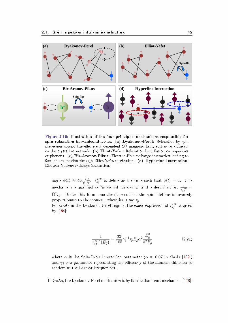
2.1. Spin injection into semiconductors 45
Dyakonov-Perel (a) Elliot-Yafet
Spin-flip
(b)
(c) Bir-Aronov-Pikus
h+ h+
Spin-flip
(d) Hyperfine Interaction
n
n n
n
n
n
n n
n n
n
n
n
e- e-
ₓ
ₓ
ₓ
Figure 2.16: Illustration of the four principles mechanisms responsible for
spin relaxation in semiconductors. (a) Dyakonov-Perel: Relaxation by spin
precession around the eective ~k dependent SO magnetic eld, and so by diusion
on the crystalline network. (b) Elliot-Yafet: Relaxation by diusion on impurities
or phonons. (c) Bir-Aronov-Pikus: Electron-Hole exchange interaction leading to
fast spin relaxation through Elliot-Yafet mechanism. (d) Hyperne Interaction:
Electron-Nucleus exchange interaction.
angle φ(t) ≈ δφ√
tτp. τDPsf is dene as the time such that φ(t) = 1. This
mechanism is qualied as "motional narrowing" and is described by: 1τDPsf
=
Ω2τp. Under this form, one clearly sees that the spin lifetime is inverselyproportionate to the moment relaxation time τp.For GaAs in the Dyakonov-Perel regime, the exact expression of τDPsf is givenby [168]:
1
τDPsf
(E~k) =
32
105γ−1
3 τpE~kα2E3~k
~2Eg(2.24)
where α is the Spin-Orbit interaction parameter (α ≈ 0.07 in GaAs [169])and γ3 is a parameter representing the eciency of the moment diusion torandomize the Larmor Frequencies.
In GaAs, the Dyakonov-Perel mechanism is by far the dominant mechanism [170].

46Chapter 2. Conversion of a magnetic information into light
polarization information using spin-injected III-V semiconductors
2.1.3.2 Elliot-Yafet
The Elliot-Yafet (EY) mechanism treats the spin relaxation of the electrons bydiusion in the crystalline network (Figure 2.16 (b)). It requires a SO interactionto couple the electron spin wave function with the lattice wave function. The SOcoupling Hamiltonian is given by:
HEY =~
4m2c2∇VSC × p · σ (2.25)
where VSC is the spin-independent scalar periodical potential of the lattice, p =
−i~∇ is the linear moment operator and σ is the Pauli matrix. The Bloch wavefunctions are not described by one eigen state of σz but by a combination of spin-up |↑〉 and spin-down |↓〉 states. Accordingly, each time a collision between anelectron and a network impurity, a default, a phonon, etc... occurs, the spin-ipprobability is non-zero. In the case of III-V semiconductors, this spin-ip probabilityis characterized by a spin lifetime τEYsf given by [171]:
1
τEYsf(E~k) = A
(∆SO
Eg + ∆SO
)2(E~kEg
)2 1
τp(E~k) (2.26)
where A ≈ 1 is a numerical factor traducing the type of diusion mechanism in-volved (charged impurity, neutral impurity, phonon, e−−h+ recombination, etc· · · ),τp(E~k) is the characteristic moment relaxation time at the energy E~k, Eg is the en-ergy band gap of the semiconductor and ∆SO is the valence band splitting parameterinduce by the SO coupling. Equation (2.26) highlights how the increase of the semi-conductor gap and the SO coupling reinforce the impact of the EY mechanism. Fora degenerate semiconductor: E~k = EF while for a non degenerate semiconductor:E~k ≈ kBT . But in both cases: τEYsf ∝ τp.
For degenerate SC, the temperature evolution of τEYsf and τp are similar. For a
non-degenerate SC, the temperature evolution of τEYsf is given by: 1τEYsf (T )
∝ T 2
τp(T )
except in the case of diusion on charged impurities where: 1τEYsf (T )
∝ T 1/2.
2.1.3.3 Bir-Aronov-Pikus
The Bir-Aronov-Pikus (BAP) mechanism describes the spin relaxation of conduc-tion electrons in p-type semiconductors [172]. The exchange interaction creates acoupling between the wave functions of a spin-up electron
(+1
2
)and a spin-down
hole(−3
2
). It acts as an eective magnetic eld which stimulates electrons spin pre-
cession and results in spin relaxation (Figure 2.16 (c)). The BAP relaxation ratesincreases with the degree of spatial overlap between electron and hole. Th spatialoverlap increases at low temperatures and for larg conning potentials such as QWsand QDs [84].

2.1. Spin injection into semiconductors 47
2.1.3.4 Hyperne interaction
The hyperne interaction rises from the exchange interaction between the spin ofelectrons and nuclear spin of atoms in the crystalline lattice (Figure 2.16 (d)). Itnaturally requires for the total nuclear spin to be non-zero Sn 6= 0 which is the casein GaAs where SGaAsn = 3
2 per atom. The eective magnetic eld generated by thehyperne interaction is given by:
~Bn =2µ0
3
g0
gµB∑i
~γn,i~S · ~Iiδ(~r − ~Ri
)(2.27)
where µ0 is the vacuum permeability, g0 = 2.0023 and g are the free and eec-tive electron Landé factor respectively, µB is the Bohr magneton and γn,i is nucleargyromagnetic factor. i identies the considered nucleus in position ~Ri while ~S and~Ii are the spin operators of the electron and the nucleus respectively.
Generally in semiconductors, the inuence of the hyperne interaction on the globalspin relaxation is negligible compared to the impact of mechanisms originating fromSO (DP, EY). Indeed, its leverage is highly diminished by the motional narrowingphenomenons [173]. Nevertheless its contribution can become signicant when thenucleus polarization increases in case of optical pumping for example [174, 175, 176].
2.1.3.5 Spin relaxation in conned potentials: QW and QD
This Ph.D project focuses on the study of spin injection in LED and VECSELswith AlGaAs/GaAs and InGaAs/GaAs QW active mediums. Consequently, it isnecessary to pay closer attention to the spin relaxation mechanisms occuring in theparticular case of conned potentials. Indeed, as the three relaxation mechanismsinduced by SO (DP, EY and BAP) are inuenced by factor such as mobility, chargelocalization or the band-structure, the spin dynamics of the electrons signicantlychanges in conned potentials compared to bulk material [84].
It has been shown that heterovalent QW displays spin relaxation times orders ofmagnitude lower than homovalent QW. Additionally, reduced spin-relaxation rateshave been observed in QW structures where spatial separation of electrons and holesis achieve using modulation-doped double heterostructures [177] or bias [178]. Thisincrease of the spin relaxation time can be associated with the inhibition of the BAPmechanism.
More specically, studies on the AlGaAs/GaAs QW revealed that the spin relax-ation time of the electrons depends weakly on the temperature for narrow wells(< 10nm). In the case of wider wells, the temperature dependance of the spinrelaxation approaches the bulk GaAs which follow a 1
T 2 law [179]. Likewise ex-periments conducted at room temperature with AlGaAs/GaAs QW showed that

48Chapter 2. Conversion of a magnetic information into light
polarization information using spin-injected III-V semiconductors
the quantum connement strongly enhances the spin relaxation with variations asfunction of the connement energy of the form E−2
conf. [179, 180]. This observation iscounter intuitive as one would expect the spin lifetime to increase with the quantumconnement. Indeed a restriction of the electron's motion in the lattice reduces theimpact of the dominant DP mechanism. In the case of QD Spin-LED [181] for ex-ample, this can even lead to temperature-independent spin-polarization unlike QWSpin-LED where the temperature dependence has clearly been demonstrated [93].
Finally, in low-dimensional semiconductor structures the hyperne interaction be-comes relevant by depolarizing the localized electrons. The spin dynamics of anelectron conned in a QD is almost not inuenced by DP, EY and BAP mech-anisms. The only spin depolarizing mechanisms remaining are the electron-holeexchange interaction and the Hyperne interaction. In these systems, spin lifetimeup to the milli-second have been observed [182].

2.2. From matter to light: Conversion of spin accumulation into lightpolarization information 49
2.2 From matter to light: Conversion of spin accumula-
tion into light polarization information
We described in the previous secion dierent methods to creat a spin-accumulationin a semiconductor. Now we focus on ways to eciently convert the spin-bit gen-erated by the spin accumulation into light polarization information. Historically,research on the optical detection of a spin signal were motivated by the necessity toby-pass the impedance mismatch issue faced for an electrical detection through at aSC/F interface. Adjusting the RA product on both the injection and the detectioninterfaces to match the electrical spin injection and detection conditions is quitechallenging. Replacing the electrical detection by an optical detection remove theconstraint on the detection and enable to measure an unbiased value of the spininjection in the SC. Additionally, the optical detection condition τr << τs is easierto fulll than the electrical detection condition τd << τs, where τr is the recombi-nation time in the active medium, τd the spin dwell time in the semiconductor canaland τs the spin-lifetime.
In this section the conversion of a spin accumulation into light polarization infor-mation is investigated. After describing the mechanisms engaged behind the opticaldetection of a spin-polarized current in a III-V semiconductor, a device orientedstudy is conducted on Spin-LEDs and Spin-LASERs.
2.2.1 Optical detection of a spin-polarized current in a III-V semi-conductor
In spin-polarized light sources, a transfer of a spin-polarized electrons (e−) operatesfrom a magnetic contact into a non-magnetic n-i-p semiconductor structure throughdrift and diusion mechanisms. After thermalization, they recombines radiativelywith unpolarized holes (h+) injected from a non-magnetic contact in the activemedium of the structure (Bulk, QWs or QDs). If the carriers spin lifetime τs isgreater than the recombination time τr in the active medium of the n-i-p diode, theresulting electroluminescence (EL) will exhibit a net circular polarization accordingto the optical quantum selection rules. Then, the degree of circular polarization(DoCP) of the emitted light can be analyzed and used as a probe for the character-ization of the spin polarized carriers population.
In this sub-section we discuss the operation principles and the general consider-ations for the design of spin-polarized light sources. I would like to acknowledgethe brilliant review written by M. Holub and P. Bhattacharya's on "Spin-polarizedlight-emitting diodes and lasers" that stands out as a reference paper on the sub-ject. Most of the fundamental informations displayed further are extracted fromthis reference [84].
50Chapter 2. Conversion of a magnetic information into light
polarization information using spin-injected III-V semiconductors
2.2.1.1 General properties of III-V semiconductors
Energy bands of semiconductors
In a semiconductor, the energy bands of the crystal are either accessible (conductionband, valence band) or non accessible (band gap). One can rebuild the energy dia-gram of the semiconductor by determining some key parameters, such as the bandgap energy and the eigen states associated with high symmetries ~k wave vectors,thanks to optical measurements (Figure 2.17 (a)).
An intrinsic (pure crystal) semiconductor is characterized by having its Fermi levelin the middle of the energy band gap. Generally, only the rst few bands aboveand below the Fermi level matters when studying the conduction properties of thematerial. Theoretically at 0 K, the lowest energy bands do not participate to theelectronic conduction and are lled according to the Pauli exclusion rule while theupper energy bands stay empty. This framework of electronic distribution can betuned by adding doping impurities in the semiconductor to manipulate the crystal'selectrons concentration. Adding a sucient concentration of electron-acceptor im-purities in the semiconductive matrix will decrease the band lling and enable theFermi level to enter the Valence Band (VB) where electrical conduction is enabledby holes. Oppositely, introducing "electron-donor" impurities will drive the Fermilevel into the Conduction Band (CB) where the electrical current is ran by conduc-tion electrons. For classical semiconductors, the band gap energy is usually around 1eV: EGaAsg = 1.5 eV , EInPg = 1.34 eV , ESig = 1.1 eV and EGeg = 0.7 eV (Figure 3.2).
Taking into account the Spin-Orbit interaction, an electron traveling in the semi-conductor crystal is characterized by the following Hamiltonian:
~H =~p2
2m0− qV (~r)− q~
4m0c2(∇V × ~p) · σ (2.28)
where V (~r) is the crystalline potential, ~p is the electron momentum quantityvector and σ the Pauli matrix. The solution of the Schrodinger equation associatedwith this Hamiltonian can be nd applying the "~k · ~p-method". This approach isparticularly powerful for the calculation of the excited states at the center of theBrillouin zone (Figure 2.17 (a)).
Notion of eective mass
In semiconductors the number of free carriers, either electrons in the CB or holesin the VB, are generated by thermal agitation or by adding doping impurities. Thecarriers concentration never exceeds 1020 cm−3 while the DOS available in a givenband is around 1022 cm−3 (like in metals). Thus, the electrons and holes occupy asmall percentage of the CB and the VB respectively and are concentrated on low

2.2. From matter to light: Conversion of spin accumulation into lightpolarization information 51
(b)
p-type
Valence Band
s-type
Conduction Band
p-type
Conduction Band
Energy
hh
lh
SO
Δ0
Eg
Esp Ec
Δ1
(a)
L Γ Λ Δ X
GaAs
Γ1
Γ1
Γ15
Γ15
X1
X3
X5
X1
X3
L1
L1
L1
L1
L3
L3
Figure 2.17: (a) Schematic band structure of direct gap III-V semiconductors near
k=0. Figure adapted from [67] (b) Ab-initio calculations of the electronic band struc-
ture of GaAs along lines of symmetry in the rst Brillouin zone. Figure reprinted
from [183].
energy states. Consequently, the study of semiconductors properties usually focuseson the energy spectra close to the CB minimum and the VB maximum. If thesetwo local extrema are energetically aligned in k = 0 (Γ-point) at the center of theBrillouin zone, the semiconductor has a direct gap (GaAs, InP,...) and oers inter-esting radiative e− - h+ properties for optoelectronic applications (Figure 2.17 (b)).
In the approximation of the "eective mass", the CB and VB around these ex-trema can be considered parabolic and the dispersion relation associated are givenby:
Ec(p) =
p2
2mc,for the CB
Ev(p) =p2
2mv,for the VB
(2.29)
where mc and mv are electrons eective mass in the CB and the VB respectively.The periodical crystalline potential can be neglect if: (i) the spatial variations of
external forces induced by an applied electric or magnetic eld are small comparedto the spatial variations created by the periodical crystalline potential and (ii) if thecarriers energy stays relatively small compared the gap energy Eg of the semicon-ductor. In this case, the carriers are considered as free particles with an eective

52Chapter 2. Conversion of a magnetic information into light
polarization information using spin-injected III-V semiconductors
Figure 2.18: Map of
the main III-V semicon-
ductors according to the
lattice parameter and
the band gap energy.
mass slightly dierent from their free particle mass. For GaAs mc = 0.067m0 butthe value is anisotropic according to crystalline symmetries and strains.
Band Structure of III-V semiconductors
Most of III-V semiconductors such as GaAs and InP display a Zinc-Blende structurewith a direct gap (Figure 2.17 (b)). The VB is divided into three valleys energeticallyclose (Heavy Holes - HH, Light Holes - LH and Split-O - SO) while the CB issplitted into two groups of valleys with a signicant energy dierence. At the Γ-point (k = 0), in the CB the lower energy band states respond to s-type orbitals(l = 0) while the corresponding states in the VB are p-type orbitals (l = 1) triply-degenerated (ml = -1, 0, +1). For the VB:
EHH(k) = ~2(A+B)k2 for Lz = ±1 and ELH(k) = ~2Ak2 for Lz = 0
∂2EHH∂k2
=1
mHH<
∂2ELH∂k2
=1
mLH⇐⇒ mLH < mHH
(2.30)
with A and B Hamiltonian constants verifying B < 0 and A+B > 0. The bandwith the highest eective mass (Lz = ±1) is called the Heavy Hole Band (HH) whilethe one with the lowest eective mass is called the Light Hole Band (LH).
However, the consideration of the Spin-Orbit interaction modies the band diagram.Indeed ~L and ~S are no more conserved separately and one has to consider the vec-torial sum ~J = ~L+ ~S and the eigen values of ~J2: j(j + 1) with |l − s| ≤ j ≤ |l + s|.The lowest s-type (l = 0) energy band of the CB stays independent from the SOinteraction contrary to the p-type VB (l = 1) that is directly aected and dividesinto sub-bands j = 1
2 and j = 32 in k = 0. The band associated with j = 3
2 is

2.2. From matter to light: Conversion of spin accumulation into lightpolarization information 53
Semi- Gap 0K/300K Mobility e− Mobility h+ m∗/m0 m∗/m0 εs/ε0
conducteur (eV) 300K (cm2/V.S) 300K (cm2/V.S) e− h+
GaAs (D) 1, 52/1, 42 8500 400 0, 067 0, 082 13, 1
InP (D) 1, 42/1, 35 4600 150 0, 077 0, 64 12, 4
Si (I) 1, 17/1, 12 1500 450 ‖0, 98 0, 16lh 11, 9
⊥0, 19 0, 49hh
Ge (I) 0, 74/0, 66 3900 1900 ‖1, 64 0, 04lh 16
⊥0, 082 0, 28hh
Table 2.2: Transport datas for electrons and holes in four semiconductors typically
used to study spin injection. Table extracted from [67]
four time degenerated jz = −32 , −
12 ,
12 ,
32 (LH-band + HH-band for both spin
orientation). The HH-band and the LH-band can be assimilated to parabols fork 6= 0 and are described by:
EHH(p) =
p2
2mHHfor Jz = ±3
2
ELH(p) =p2
2mLHfor Jz = ±1
2
(2.31)
The band of lower energy j = 12 is two time degenerate jz = −1
2 ,12 and is called
the Split-O band (Figure 2.17 (b)). In k = 0, it is separated from the HH-band andthe LH-band by an energy included 0.1 to 1 eV depending on the atomic number ofthe III-V semiconductor's cation. In GaAs ∆0 = 0.34 eV while in InP ∆0 = 0.11
eV.
2.2.1.2 Spin information conversion through quantum opto-electrical
mechanism
In Spin-LEDs and Spin-LASERs emission of circularly polarized light originatesfrom radiative recombinations of spin polarized electrons with unpolarized hole inactive mediums such as QWs. The spin polarization is directly related to the opticalpolarization through the optical quantum selection rules governing radiative recom-bination. There is a proportionality relation between the spin polarization of theinjected current Ps and the DoCP of the emitted light Pcirc when the ferromagneticlayer magnetization and the optical measurement direction are parallel to the QWsquantication axis (growth direction) [29, 184, 92, 99, 98]. The annihilation of ane− - h+ pair during the inter-band recombination process triggers a transfer of thetotal electron-hole angular momentum to the emitted photon. In ~ units, polarizedphotons have an angular momentum projection on the wave vector direction equalto +1 or 1 respectively. Thus the radiation resulting from the recombination of thespin-polarized carriers will be partially circularly polarized if the spin orientation
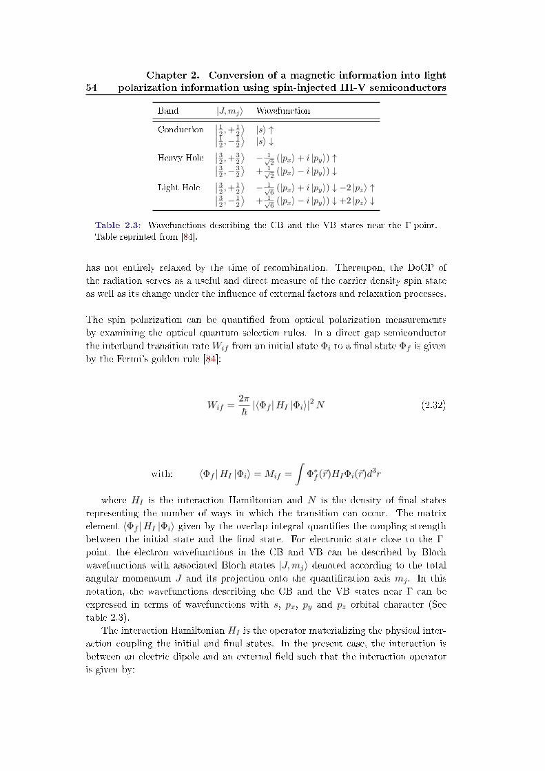
54Chapter 2. Conversion of a magnetic information into light
polarization information using spin-injected III-V semiconductors
Band |J,mj〉 Wavefunction
Conduction∣∣ 1
2 ,+12
⟩|s〉 ↑∣∣ 1
2 ,−12
⟩|s〉 ↓
Heavy Hole∣∣ 3
2 ,+32
⟩− 1√
2(|px〉+ i |py〉) ↑∣∣ 3
2 ,−32
⟩+ 1√
2(|px〉 − i |py〉) ↓
Light Hole∣∣ 3
2 ,+12
⟩− 1√
6(|px〉+ i |py〉) ↓ −2 |pz〉 ↑∣∣ 3
2 ,−12
⟩+ 1√
6(|px〉 − i |py〉) ↓ +2 |pz〉 ↓
Table 2.3: Wavefunctions describing the CB and the VB states near the Γ-point.
Table reprinted from [84].
has not entirely relaxed by the time of recombination. Thereupon, the DoCP ofthe radiation serves as a useful and direct measure of the carrier density spin stateas well as its change under the inuence of external factors and relaxation processes.
The spin polarization can be quantied from optical polarization measurementsby examining the optical quantum selection rules. In a direct gap semiconductorthe interband transition rate Wif from an initial state Φi to a nal state Φf is givenby the Fermi's golden rule [84]:
Wif =2π
~|〈Φf |HI |Φi〉|2N (2.32)
with: 〈Φf |HI |Φi〉 = Mif =
∫Φ∗f (~r)HIΦi(~r)d
3r
where HI is the interaction Hamiltonian and N is the density of nal statesrepresenting the number of ways in which the transition can occur. The matrixelement 〈Φf |HI |Φi〉 given by the overlap integral quanties the coupling strengthbetween the initial state and the nal state. For electronic state close to the Γ-point, the electron wavefunctions in the CB and VB can be described by Blochwavefunctions with associated Bloch states |J,mj〉 denoted according to the totalangular momentum J and its projection onto the quantication axis mj . In thisnotation, the wavefunctions describing the CB and the VB states near Γ can beexpressed in terms of wavefunctions with s, px, py and pz orbital character (Seetable 2.3).
The interaction Hamiltonian HI is the operator materializing the physical inter-action coupling the initial and nal states. In the present case, the interaction isbetween an electric dipole and an external eld such that the interaction operatoris given by:

2.2. From matter to light: Conversion of spin accumulation into lightpolarization information 55
HI = ~µ · ~E = µxEx + µyEy + µzEz (2.33)
where ~µ is the dipole moment and ~E is the electric eld of the light wave. Thecomponents of the electric eld Ex, Ey and Ez are considered constant as the electriceld variations are small compare to the periodical variation of the lattice potential.When the vector operator ~µ is expressed as a spherical tensor µ1
±1 for σ± opticaltransition, the Wigner-Eckart theorem enunciate that the non-zero matrix element(〈Φf |HI |Φi〉 6= 0) are the terms verifying the relation ∆mj = ±1 [84]. Then in sur-face emitting devices, the conservation of angular momentum for mj = ±1 radiativetransition imposes the generation of σ∓-polarized photon. The transition probabil-ities for allowed transitions are given in table 2.4. The orientation convention is toconsider a photon right circularly polarized σ+ (respectively left circularly polarizedσ−) when emitted from a ∆mj = −1 transition and propagating toward the surface(respectively toward the backside). The optical selection rule are only strictly validat the Γ-point. By moving away from Γ the HH and LH band mixture results in anon-ideal optical polarization.
At Γ, the CB → HH transition are three times more probable than the CB →LH transition regardless to the active medium nature (Table 2.4 & Figure 2.19(b)). In a bulk semiconductor the HH-band and the LH-band are degenerate in Γ
which intrinsically limit the DoCP to half the value of the spin polarization degreeinjected in the device (Figure 2.19 (a)). Thus, the maximum value theoreticallyreachable for Pcirc with a bulk active medium will be limited to 50% for a carrier'sspin polarization of 100% [84]:
Pcirc =I(σ+)− I(σ−)
I(σ+) + I(σ−)=
(3n↓ + n↑)− (3n↑ + n↓)
(3n↓ + n↑) + (3n↑ + n↓)=
n↓ − n↑2(n↑ − n↓)
= −Ps2
(2.34)
where I(σ+) and I(σ−) are the intensities for σ+- and σ−-polarized light respec-tively. n↑ and n↓ stands for the DOS of spin-up and spin-down electrons respectively.
The case of QWs is much more appealing as the quantum connement andpotential epitaxial strain lift the degeneracy between the HH-band and the LH-band in Γ. For AlxGa1−xAs and InxGa1−xAs, that we extensively used in the activemedium of Spin-LEDs and Spin-VECSELs, the HH-band is energetically higher thanthe LH-band. Consequently the LH states can be ignored, especially since the CB→ HH transitions are three times more probable than the CB → LH transitions. Itis then theoretically possible to reach 100% DoCP for an injected spin polarizationof 100% [84]:
Pcirc =I(σ+)− I(σ−)
I(σ+) + I(σ−)∼=
3n↓ − 3n↑3n↓ + 3n↑
=n↓ − n↑n↓ + n↑
= −Ps (2.35)

56Chapter 2. Conversion of a magnetic information into light
polarization information using spin-injected III-V semiconductors
Interband Matrix element ∆mj Emission Transition
Transition Mij Polarization Probability |Mij |2
CB↑ −→ HH↑⟨
32 ,+
32
∣∣µx ∣∣ 12 ,+ 12
⟩-1 σ+ 1
2 | 〈px|µx |s〉 |2
CB↓ −→ HH↓⟨
32 ,−
32
∣∣µx ∣∣ 12 ,− 12
⟩+1 σ− 1
2 | 〈px|µx |s〉 |2
CB↑ −→ LH↓⟨
32 ,−
12
∣∣µx ∣∣ 12 ,+ 12
⟩+1 σ− 1
6 | 〈px|µx |s〉 |2
CB↓ −→ LH↑⟨
32 ,+
12
∣∣µx ∣∣ 12 ,− 12
⟩-1 σ+ 1
6 | 〈px|µx |s〉 |2
Table 2.4: Interband transitions probabilities and related polarization of the emitted
photon. Table reprinted from [84].
Nevertheless, in the permanent regime, the spin polarization in the active mediumis not immediately converted into optical circular polarization. The conversion pro-cess is governed by a recombination time τ characteristic of the active region with1τ = 1
τr+ 1
τnrwhere τr and τnr are the radiative and non-radiative recombination
rate respectively. In the case where the spin relaxation time τs is shorter than therecombination time: τs << τ , the spin information will be lost through relax-ation mechanisms before the carriers recombine. Thus, when trying to extract thespin polarization degree of the injected carriers from the emitted light DoCP, it isnecessary to introduce a renormalization factor F = 1
1+ ττs
taking into account the
relative variation of the characteristic life times:
Ps =1
F· Pcirc =
(1 +
τ
τs
)· Pcirc (2.36)
This relation enables us to directly use the emitted light DoCP as a probe forthe measurement of the injected carriers spin polarization degree and is used tocharacterize the injection eciency of the ferromagnetic spin injectors. Nevertheless,as the depolarization mechanisms occurring during transport from the injector thethe active medium are not taken into account, this only provides us an inferior limitvalue of the spin injection eciency (see section 2.2.1.4).
2.2.1.3 Circularly-Polarized Optical Pumping
Circularly-polarized optical pumping stands out as a corner stone of the spin in-jection in III-V optoelectronic devices. This mechanism enables the generation ofspin polarized carrier by engaging light/matter interactions. We used it extensivelyduring our experiments and it deserve a particular attention.
Under optical pumping, the electron gas of a semiconductor medium is photoexcitedbetween dierent energy levels by absorption of the incident light. The technique wasdeveloped by 1966 Nobel Laureate Alfred Kastler in the early 1950s [185, 186, 187].

2.2. From matter to light: Conversion of spin accumulation into lightpolarization information 57
Figure 2.19: Optical Quantum selection rules for dipole radiation: (a) In
the case of a bulk active medium, the HH-band and LH-Band are degenerated and a
CB→HH recombination is three times more probable than a CB→LH recombination.
(b) In QWs, the epitaxial strain and quantum connement lift the degeneracy between
the HH-band and LH-Band. The energetically favored transition becomes CB→HH
and if the bands are separated by an energy at least several times the thermal energy:
Pcirc = Ps
The inuence of the light polarization on the spin generation in the active mediumwas highlighted by Lampel in 1968 [188]. In the context of lasers, the goal is toachieve a population inversion in the gain medium to obtain optical amplicationvia stimulated emission for some range of optical frequencies. The width of thatrange is called the gain bandwidth.
In case of Spin-LEDs and Spin-VECSELs, optical pumping is used to cyclicallypump electrons bound within a well-dened quantum state. Generally, the quan-tum connement is ensured by quantum well structures based on binary (GaAs,GaN , InP , InAs, ZnSe, ...) or ternary (AlxGa1−xAs, InxG1−xAs, AlxGa1−xP,GaAsP, ...) direct gap semiconductors. For the simplest case of coherent two-leveloptical pumping in a semiconductor band structure, this means that the electronis coherently pumped from the valence band (VB) to the conduction band (CB).Due to the cyclic nature of optical pumping the bound electron will actually beundergoing repeated excitation and decay between VB and CB.
As light absorption is the exact reverse mechanism of radiative recombination, thegeneration of spin-polarized carriers by absorption of circularly polarized light fol-lows the same functioning pattern and obey to the same quantum selection rules.Consequently the reader can relate to the previous section for more details on themechanism involved. The key for an ecient optical spin-injection in a semicon-ductor relies on the optical quantum selection rules for dipole radiation associatedwith the conservation of angular momentum z-projections mz occurring in conned

58Chapter 2. Conversion of a magnetic information into light
polarization information using spin-injected III-V semiconductors
QW
Substrate
n-doped layer
Barrier
Barrier
p-doped layer
Optoelectronic
Structure
σ+
σ-
Right or Left circularly
polarized pump light Conservation of angular momentum: mZ = 1
Figure 2.20: Scheme of the circularly polarized optical pumping mechanism:
Spin generation happens through preferential transition driven by the optical quantum
selection rule in the active medium (QW) of the optoelectronic device.
strained active medium or Quantum Wells (QWs) [30]. The allowed transitions arequantied by ∆mz = ±1. In QWs, the lift of degeneracy between the Heavy Hole(HH) band and the Light Hole band (LH) leads to preferential spin-polarized carri-ers generation by absorption of circularly polarized photons between the HH-bandand the Conduction Band (CB). The absorption of left circularly polarized lightσ− of intensity Iσ− (respectively right circularly polarized light σ+ of intensity Iσ+)results in the generation of spin-↑ electrons with an associated DOS at the Fermilevel n↑ (respectively spin-↓ with an associated DOS at the Fermi level n↓) for theHH(+3/2)→ CB(+1/2) transition (respectively HH(−3/2)→ CB(−1/2) transi-tion). The spin polarization degree of the optically injected electrons can be thendened by P opts = (n↑ − n↓)/(n↑ + n↓) (Figure 2.20). While in bulk GaAs a 50%spin polarization can be induced at best, a P opts close to a 100% can theoreticallybe achieved in QWs. Thus, on a pure spin injection eciency point of view, spininjection using circularly polarized optical pumping oers an interesting solution toovercome the limitations faced with direct injection where the eciency is limited bythe intrinsic spin polarization of the ferromagnetic PFs and the interface resistancer∗b .
It is important to note that the quantum selection rules are strictly valid atthe Γ-point of the band structure. Additionally, to prevent the spin mixing andmaximize P opts the incident photons energy needs to be higher than the band gapenergy but not high enough to excite carriers from the split-o band. The absorp-tion coecient α = A∗
√hν − Eg of the material at the wavelength λ = v
ν also playsa fundamental role in the conversion eciency of the angular momentum. Finally,the incidence of the pump beam should be normal to the devices active medium inorder to prevent any elliptical projection of the circular polarization ("end pump-ing") which would signicantly reduce the mechanism performances.

2.2. From matter to light: Conversion of spin accumulation into lightpolarization information 59
Even though semiconductor optoelectronic devices are commonly electrically pumpedfor application requirement, optical pumping oers certain advantages. For exam-ple in the case of VECSELs, it allows for a laser output with very high brightness(high power combined with high beam quality). In other cases, optical pumping issometimes used for testing purposes, e.g. when new semiconductor compositions areinvestigated. Optically pumped semiconductor gain media generally have a simplerstructure than their electrically pumped counterparts.
2.2.1.4 Design of spin-polarized light sources
General considerations
The rst parameter to address is the distance between the spin injector and theactive medium of the device.
The travel time between the ferromagnetic spin polarizer and the QWs needsto be as short as possible to maximize the spin collection and minimize the spindepolarization through relaxation mechanisms. The dependency of spacer thicknesson the spin injection eciency was experimentally witnessed in a study investigatinganisotropic spin injection in an InGaAs QW Spin-LED with GaMnAs spin-injector.A monotonic increase from 0.5% to 7% in the polarization was measured as thespacer thickness decreased from 420 nm to 20 nm [189]. This results clearly high-lights that the spacer thickness should be minimized in order to maximize the spinconversion. However, in practice a compromise has to be found between minimiz-ing the spin transport length and limiting the interdiusion of magnetic impuritiesinto the active region. The contamination of the recombination area can potentiallyresult in unwanted parasitic polarization which could bias the measurement of theemitted light DoCP or even mask the evidence of spin injection [84].
The second signicant criterion to consider is the emitting geometry of the device:
Surface-emitting geometry: This geometry has been applied for the architec-ture of every Spin-LEDs and Spin-VECSELs used during this Ph.D thesis. It oersat least two advantages over an edge-emitting geometry. The major one concern theoptical quantum selection rules: heart of the conversion mechanism, they are muchmore straightforward in the Faraday geometry due to considerations on the pro-jection of the angular momentum. In QWs the quantum connement and reducedsymmetries pull the angular momentum of the HH-states along the quanticationaxis (along the surface direction). Thus, the spin orientation of the injected elec-trons should also be parallel to the quantication axis and the conservation of theangular momentum has to be analyzed along the z-axis. Secondly, a surface-emittinggeometry oers a short escape distance (≈ 100 nm) for the photons stemming fromthe radiative recombinations which signicantly reduces photon reabsorption andrecycling. The down side of using a surface-emitting geometry lies in the passage

60Chapter 2. Conversion of a magnetic information into light
polarization information using spin-injected III-V semiconductors
of the circularly polarized emitted photons through the ferromagnetic spin aligner.The dierential absorption of right (σ+) and left (σ−) circularly polarized light inthe ferromagnetic layer introduces an articial polarization which has the potentialto distort the light DoCP measurements. This phenomenon is called Magnetic Cir-cular Dichroism (MCD) (see section 2.2.1.5). Moreover, a relatively strong appliedmagnetic eld is usually required to overcome the shape anisotropy of the ferromag-netic thin layer and drive the magnetization out-of-plane in order to polarize theinjected carriers along the z-axis. In the second part of the manuscript, we will seethat this issue can be overcome by implementing of spin-injector exhibiting intrinsicPerpendicular Magnetic Anisotropy (PMA).
Edge-emitting geometry: Prima facie this conguration seems to be the mostsuitable for applications as only modest applied magnetic eld are required for spinmanipulation. Indeed, the shape anisotropy of the ferromagnetic thin lm restrictsthe easy magnetization axis in-plane. The device can operate in a remanent stateand easily switched with a weak magnetic eld (induced by a command electrical linefor instance). Nevertheless, the main handicap of this architecture is the orthogonalorientation between the connement axis and the spin polarization of the injectedcarriers. This geometry considerably reduces the spin conversion eciency throughthe optical quantum selection rules. Additionally, the light has to travel distancesthat can potentially exceeds several 100 µm to escape the structure. This opens thedoor to strong photons reabsorption and complicate the precise quantication ofspin polarization from optical polarization measurements [84]. Nonetheless, despitethe reduced eciency of the quantum selection rules in edge-emitting geometry,spin injection performances competitive with the values obtained in surface-emittinggeometry were experimentally demonstrated in AlGaAs/GaAs QW Spin-LEDs [190].
Active region - Spin detection medium
One can instinctively understand that the structure and composition of the activemedium of the spin-polarized light source considerably inuence the operating char-acteristics of the device. The ideal active medium would display an almost innitespin lifetime τs compare to the radiative recombination time τr to reach a 100%information conversion eciency. As explain in section 2.1.3.5, τs tends to signi-cantly increase with the carrier connement due to the inversely related impact ofthe spin relaxation mechanism. Naturally, when walking through the state-of-the-artof spin-polarized light sources, QWs and QDs clearly stands out the dominant choicefor active mediums. They combine: (i) a strong carrier spatial localization (depthresolution) and (ii) the generation of photons easily distinguishable from other spec-troscopic features arising from emission in other region of the heterostructure thanksto the smaller band gap of the QWs compare with the bulk material. This also hasthe advantage to limit the photons interactions with the heterostructure and mini-mizing the MCD re-absorption.

2.2. From matter to light: Conversion of spin accumulation into lightpolarization information 61
The trend goes preferentially to the use of lattice-matched AlGaAs/GaAs or In-GaAs/GaAs QW wherein optical quantum selection rules can immediately ap-ply. The strains active medium should be avoid as recombination dynamics candeviate signicantly from the textbook case and reduce the spin conversion e-ciency [191, 192]. It was theoretically predicted that for 100% spin-polarized injectedelectron a maximum proportionality factor Ps
Pcircis achievable even at low tempera-
tures [191]. The QWs growth direction ((100) or (110)) also plays a key role in thespin relaxation time. Spin lifetimes of the nanosecond order at room temperaturewere experimentally measured in (110)-GaAs QWs Spin-LEDs as a consequence ofthe inhibition of the DP relaxation mechanism. This is more than an order of mag-nitude longer than that of the (100) counterparts [193]. In QWs the increase of τrand the decrease τs associated with the increase of temperature and bias tend todecrease the τr
τsratio. For a considered carrier initially spin polarized, the condition
τr ≥ τs leads to a loss of the spin information before the radiative recombination oc-curs and so to an average decrease of Pcirc. At constant bias the variations of τr andτs relative to one another with the temperature x the global dynamics evolution ofPcirc. Consequently, it is necessary to take into account the τr
τsratio to accurately
quantify the injected spin polarization from optical measurements (eq. 2.36). It isalso observe that as either the temperature or bias increases, Pcirc further decreases.Particularly since thermal spreading of the carrier distribution results in the occu-pation of the QW light-hole bands and the occupation of non-zero quasi-momentumstates were band maxing arises [84].
The active medium of the devices used during the thesis were based on: (i) AlxGa1−xAs/GaAs and InxGa1−xAs/GaAs QWs for the Spin-LED and (ii) strained In22%Ga78%As/GaAs95%P5% QWs for the VECSEL. The use of strained-balanced QWs in the caseof lasers enables to stack more QWs in the active medium without adding any strainswhich would induce dislocations and thus reduce the carrier lifetime. But as we willsee in the fourth chapter, circularly polarized mode stabilization issues arise fromthe lattice strains.
2.2.1.5 Measurements considerations
Detection geometries
Three measurement geometries are typically employed for the characterization ofspin-polarized light sources: Faraday, Voigt and oblique Hanle eect. The bestconguration for a particular experiment is determined by the details of the het-erostructure and device design.
Faraday geometry: This geometry was used for all the measurement performedduring the Ph.D. project. It is commonly the most used geometry as the opticalselection rules are straightforward in this conguration allowing a direct readout ofthe spin injection eciency (Figure 2.21 (a)). In most cases, this conguration is

62Chapter 2. Conversion of a magnetic information into light
polarization information using spin-injected III-V semiconductors
associated with the need to apply an external magnetic eld to overcome the spininjector shape anisotropy and align the magnetization out-of-plane parallel to thequantication axis. A eld of few Tesla can easily create a sizable Zeeman splittingof the CB and the VB states in the QWs and induce a parasitic contribution to theemitted DoCP. This problem is instantly overcome if the injector naturally displaysperpendicular magnetic anisotropy.
Voigt geometry: This geometry is applied to characterize the rarely used edge-emitting Spin-LEDs (Figure 2.21 (b)). The selection rules applied in the Faradaygeometry with QWs active medium are no longer valid as the injected carriers arespin polarized in the direction perpendicular to the quantication axis. In-planespin-polarized electrons may be conceived as a coherent superposition of an equalnumber of spin-up and spin-down electrons; thus the resulting optical polarizationwill not attain a net CP when measuring along the z-axis [84].The active mediumsusable for this geometry are either QD or bulk medium and the relation betweenPs and Pcirc is no longer direct. In most cases, the performances exhibited byVoigt geometry devices are always below the results achieved with surface-emittingdevices. Pcirc levels hardly irting with 2% at low temperature (see table 2.5).The only advantage lies in the possibility of operation at magnetic remanence asmost thin lm ferromagnets easy axis is in-plane. It also avoids any magnetic eld-dependent artifacts and MCD contribution as the emission is collected through acleaved facet and does not have to pass through a ferromagnetic spin aligner.
Oblique Hanle geometry: This detection method was rst implemented onSpin-LEDs by Motsnyi et al. [109, 98]. It involves the application of an obliquemagnetic eld ~B making an angle of roughly 45 with respect to the horizontalaxis (Figure 3.5 (c)). ~B induces a precession of the carrier's spin with the Larmorfrequency ~Ω and assigns a perpendicular component to the spin vector detectablethrough the emitted light DoCP. This conguration is a clever way to eectivelydetect spin injection from an in-plane ferromagnetic contact. The application of asmall oblique ~B manipulates spins during transport suciently enough to obtain acomponent along the z-axis. In OHE geometry where the applied ~B make an angle θwith the horizontal axis, Pcirc is related to Ps through the following equation [194]:
Pcirc =I(σ+)− I(σ−)
I(σ+) + I(σ−)=
1
4· Tsτ
[(ΩTs)
2
1 + (ΩTs)2· cos(θ) +
1 + (ΩTs)2
2
1 + (ΩTs)2· sin(θ)
]· Ps
(2.37)
where the ratio Tsτ is the spin detection eciency of the active medium, Ts
being the spin life time with 1Ts
= 1τ + 1
τs, τ the e− - h+ recombination time
and τs the spin-relaxation time. This technique provides additional insights notimmediately available in the other measurement geometries. It oers the advantage
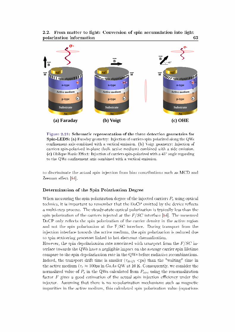
2.2. From matter to light: Conversion of spin accumulation into lightpolarization information 63
Substrate
n-type
Au
p-type
Au
M
B
σ-
(a) Faraday
e-
h+
Substrate
n-type
Au
p-type
Au
M
B
(b) Voigt
e-
h+
Substrate
n-type
Au
p-type
Au
M
σ-
(c) OHE
h+
e-
B ~ 45
Figure 2.21: Schematic representation of the three detection geometries for
Spin-LEDS: (a) Faraday geometry: Injection of carriers spin-polarized along the QWs
connement axis combined with a vertical emission. (b) Voigt geometry: Injection of
carriers spin-polarized in-plane (bulk active medium) combined with a side emission.
(c) Oblique Hanle Eect: Injection of carriers spin-polarized with a 45 angle regarding
to the QWs connement axis combined with a vertical emission.
to discriminate the actual spin injection from bias contributions such as MCD andZeeman eect [84].
Determination of the Spin Polarization Degree
When measuring the spin polarization degree of the injected carriers Ps using opticaltechnics, it is important to remember that the DoCP emitted by the device reectsa multi-step process. The steady-state optical polarization is typically less than thespin polarization of the carriers injected at the F/SC interface [84]. The measuredDoCP only reects the spin polarization of the carrier density in the active regionand not the spin polarization at the F/SC interface. During transport from theinjection interface towards the active medium, the spin polarization is reduced dueto spin scattering processes linked to hot electrons thermalization.However, the spin depolarization rate associated with transport from the F/SC in-terface towards the QWs have a negligible impact on the average carrier spin lifetimecompare to the spin depolarization rate in the QWs before radiative recombinations.Indeed, the transport drift time is smaller (τdrift <ps) than the "waiting" time inthe active medium (τr ≈ 100ps in GaAs QW at 10 K. Consequently, we consider thenormalized value of Ps in the QWs calculated from Pcirc using the renormalizationfactor F gives a good estimation of the actual spin injection eciency under theinjector. Assuming that there is no re-polarization mechanisms such as magneticimpurities in the active medium, this calculated spin polarization value (equations

64Chapter 2. Conversion of a magnetic information into light
polarization information using spin-injected III-V semiconductors
2.34, 2.35, 2.36) stands as an inferior limit of the spin injection eciency at theF/SC interface.
Additionally, only the free exciton's and free carrier's components of the opticalpolarization provide a quantitative measure of the spin polarization of the carriersinvolved in the quantum selection rule [195]. Thus, a reliable measure of the spininjection eciency can be obtained only if one takes care to spectroscopically resolveand accurately identify the free exciton and free carrier components. Other spectralfeatures such as donor- and acceptor-bound excitons, phonon replicas, recombina-tions mediated by various impurity levels or complexes (CB → Acceptor, Donor→ Acceptor, etc...), exhibit polarization characteristics which do not reect spinpolarization. These processes do not have well dened angular momentum [196].The relative intensity of these spectral components can be minimized with carefulcontrol of the heterostructure doping prole and material quality.
Spurious contribution to the Degree of Circular Polarization
When probing the spin injection eciency in a spin-polarized light source, sepa-rating real DoCP from artifacts contribution is of primary importance. Inducedcircular polarization (CP) can arise from the three main parasite mechanisms: thediusion of magnetic impurities, Magnetic Circular Dichroism (MCD) and Zeemaneect.
Even a small diusion of magnetic impurities from the ferromagnetic spin injec-tor into the active medium of the device can induce a signicant CP of the emittedlight by sporadic spin polarization or re-polarization of the electrically injected car-riers. In practice, a non-magnetic spacer of at least several tens of angstroms thickshould be introduced in between the ferromagnetic thin layer and the active regionconsidering the typical interdiusion lengths for MBE-grown structures [84]. Thiscondition is usually easily veried since the thickness of the multilayer stack (witha doping gradient) inserted in between the ferromagnet and the QWs is commonlyaround 100 nm.
In surface emitting devices, the emitted light passes trough the ferromagnetic layerused as a spin polarizer before reaching the measurement setup. The dierentialabsorption between σ+ and σ− polarized light by the ferromagnetic material in-duces Magnetic Circular Dichroism (MCD) that modies the total DoCP of theemitted light. In Spin-LEDs the MCD artefact depends on the emission angle andis rarely above 3%. The MCD contribution can be directly quantify by pumpingthe device with linearly polarized light and analyzing the Photoluminescence (PL)ellipticity. Otherwise it can be bypassed using QWs with dierent energy gap togenerate photons transparent to the rest of the device and detect the EL in a back-side conguration. In the case of Spin-VECSELs, the impact of the intra-cavitiesinjectors is suspected to be much more signicant as the number of light round trip

2.2. From matter to light: Conversion of spin accumulation into lightpolarization information 65
in the resonant cavity is considerably higher.
In most experiments, an apply magnetic eld is required to drive and switch themagnetization of the ferromagnetic spin injector. Spurious Zeeman eect can arisefrom the lift of degeneracy of the spin sub-bands within the active medium. Sincecarriers thermalize to ll the lowest energy states, the carrier density in the activeregion will attain a net spin polarization resulting in a slight CP for the emission notrelated to direct injection from the magnetic contact. Thankfully, this artifact canbe easily identify by looking at the measured DoCP when reversing the magneticeld.

66Chapter 2. Conversion of a magnetic information into light
polarization information using spin-injected III-V semiconductors
2.2.2 The Spin-LED concept
A Spin-LED is a Light Emitting Diode structure caped with a ferromagnetic spin in-jector used to spin polarized the carriers before injection in the active medium of theLED structure. The LED structure is typically a semiconductor heterostructure in-cluding an electron reservoir (n-doped region) and a hole reservoir (p-doped region)separated by a lightly doped "near" intrinsic semiconductor region. The rst signif-icant demonstration of spin injection in a LED structure was achieved by Fiederlinget al. with a II-VI DMS ferromagnetic injector on top of an AlGaAS/GaAS QWLED structure [29].
2.2.2.1 n-i-p band structure
A n-i-p semiconductor structure is a diode with a wide, lightly doped "near" intrinsicsemiconductor region between a p-type semiconductor and an n-type semiconductorregion. The p-type and n-type regions are typically heavily doped as they are usedfor ohmic contacts. The addition of an intrinsic layer changes properties of the p-njunction.
When reverse biased, a n-i-p diode enable the emission of light from the intrin-sic region. By energetically concentrating the radiative recombinations, the i-regionreduces the spectral enlargement emerging from the layers inhomogeneities. Com-pared to conventional p-n diodes, the emitted wavelength is not submitted to acommonly observed redshift when emission happens from a doped region. It is alsopossible to introduce a conned potential such as QWs or QDs in the intrinsic region(Figure 2.22). In addition of increasing the radiative recombination eciency, thisgives an additional degree of freedom to modulate the emitted wavelentgh accord-ing to the dimensions and strains of the QWs/QDs. When the diode is forwardbiased, the injected carrier concentration is typically several orders of magnitudehigher than the intrinsic level carrier concentration. Due to this high injection level(favored by the depletion process) the electric eld extends deeply (almost the entirelength) into the region. This electric eld helps to speed up the transport of chargecarriers from the P region to the N region. This process results in faster operationof the diode making it a suitable device for high frequency operations.
When reversed biased, a n-i-p diode can be use as an ultra-fast photo-detectorwith a bandwidth of several GHz. Indeed, the small carrier density in the intrinsicregion provides a relatively long lifetime to the photo-generated e− - h+ pairs bythe reason of a low recombination probability. This translates in a highly ecientphoto-generation.
Compare to conventional p-n diodes, the wide intrinsic region makes the n-i-p diodean inferior rectier (one typical function of a diode). But, on the other hand, itmakes the n-i-p diode suitable for attenuators, fast switches, photo-detectors, andhigh voltage power electronics applications.

2.2. From matter to light: Conversion of spin accumulation into lightpolarization information 67
p++
e-
h+
e- e-
Ferromagnet
Tunnel
Barrier
Tunnel Injection
n++ n
p
QW h+ i i
p++
σ-
Figure 2.22: Schematic band structure of a n-i-p Spin-LED
2.2.2.2 State-of-the-art
The very rst two Spin-LEDs were reported simultaneously by Fiederling et al. [29]and Ohno et al. [197] in 1999.
Outstanding results were already obtained with electrically injected Spin-LEDs us-ing dierent type of spin-injectors polarized in an applied magnetic eld on dierentactive mediums. As displayed in table 3.5, a degree of circular polarization Pcirc ashigh as 86% at 1.5 K was reached by Fiederling et al. using a BeZnMnSe DilutedMagnetic Semiconductor (DMS) on top of a GaAs-bulk LED in the Faraday geome-try [29]. Jiang et al. demonstrated a Pcirc = 47% at 290 K using a CoFe/MgO(100)Metal Tunnel Junction (MTJ) deposited on a AlGaAs/GaAs QW Spin-LED in aFaraday conguration with a 5 T perpendicular applied magnetic eld [99]. WithFe/(Al)GaAs Schottky barrier, Hanbicki et al. showed a Pcirc = 30% at 240 K alsoin a vertical conguration with a 3 T magnetic eld [93].
To this day, the record for highest EL DoCP at room temperature is still heldby Jiang et al. with the CoFe/MgO(100) MTJ injector. This same group alsohighlighted the weaker temperature dependence of the eciency compared to theEL DoCP using this injector. They showed a stable Ps ≈ 70% from 10 K to 300K [198]. Unfortunately, the magnetization of most thin lm ferromagnets resides in-plane due to the shape anisotropy. All these experiments required an applied ~B(T )
to drive the magnetization out-of-plane to match the operation conditions (for Fara-day congurations). This stays a strong limitation for potential applications.
So far, only a few groups have reported ferromagnetic spin injectors exhibitingPerpendicular Magnetic Anisotropy (PMA) [218, 219, 220]. Using a PMA MnGa

68Chapter 2. Conversion of a magnetic information into light
polarization information using spin-injected III-V semiconductors
Spin Injector Active Region Spin Polarization (%) Geometry Reference
FM|DMS|Heusler / Temperature (K)
CoFe/MgO GaAs QW 52%/100 K; 32%/290 K Faraday [99]
GaAs QW 70%/10-300 K Faraday [198]
GaAs QW 32%/100 K Faraday [199]
CoFe/AlOx GaAs Bulk 21%/80 K; 16%/300 K OHE [98]
GaAs Bulk 9%/80 K OHE [109]
Co/Al2O3 GaAs QW 2%/300 K Faraday [200]
Fe/AlOx InGaAs QW 15%/5 K (Switchable) Voigt [201]
Fe/GaO GaAs QW 20%/2 Faraday [202]
NiFe-CoFe/AlOx GaAs bulk 24%/80 K; 12%/300 K OHE [194]
Ni80Fe20/Al2O3 GaAs QW 0.2%/300 K Faraday [200]
Fe Schotttky InGaAs QW 78%/2 K (BB Tans.) Faraday [203]
GaAs QW 32%/4.5 K; 30%/240 K Faraday [93]
GaAs QW 30%/20 K Voigt [190]
InAs/GaAs QD 7.5%/15 K OHE [205]
InAs QD 5%/80-300 K Faraday [181]
Fe3Si Schotttky InGaAs QW 3.5%/25 K; 2%/300 K Faraday [206]
MnAs InGaAs QW 6%/80 K; <6%/300 K Faraday [207]
GaAs QW 26%/300 K Faraday [208]
MnGa w/ PMA GaAs QW 5%/2 K Faraday [209]
MnSb Schottky GaAs Bulk 20%/80 K OHE [88]
(Fe/Tb) w/ PMA InGaAs QW 0.75%/90 K Faraday [210]
GaAs QW 3%/300 K Faraday [306]
GaMnAs (holes) InGaAs QW 18%/5.1 K Faraday [212]
InGaAs QW 1%/6 K Voigt [197]
InAs QD 1%/4.5 K Voigt [213]
GaMnAs Zener GaAs Bulk 82%/4.6 K OHE [113]
InGaAs QW 6.5%/6 K Faraday [112]
InGaAs QW 0.82%/5 K Faraday [214]
InAs QD 1.2%/5 K; 0.2%/60 K Voigt [213]
ZnMnSe GaAs Bulk 86%/1.5 K; 24%/33 K Faraday [29]
GaAs QW 83%/4.5 K Faraday [195]
CdSe QD 70%/2 K Faraday [215]
InGaAs QD 21%/5 K Faraday [216]
CdCr2Se4 GaAs QW 4-6%/5 K Faraday [217]
Co2MnGe GaAs QW 27%/2 K; 2%/280 K OHE [123]
Co2.4Mn1.6Ga InGaAs QW 13%/5 K OHE [121]
Table 2.5: Comparison of state-of-the-art spin injection eciencies from various fer-
romagnetic contacts into Spin-LEDs with dierent active mediums. Table completed
from [84].

2.2. From matter to light: Conversion of spin accumulation into lightpolarization information 69
ferromagnetic layer for spin injection, Adelmann et al. showed Pcirc = 5% at 2 K ina remanent state [209]. Hovel et al. reported Pcirc = 3% at room temperature usinga rare earth based Cr/(Fe/Tb)10 spin-injector in both Schottky and Tunnel cong-uration at magnetic remanence [306]. During this Ph.D, we succeeded in setting anew world record for PMA Spin-LED operating at magnetic remanence and at roomtemperature. A DoCP Pcirc = 8% at room temperature was demonstrated using aMgO/CoFeB/Ta MTJ spin-injector on an InGaAs/GaAs QW LED structure inFaraday conguration [312] (see Chapter III).
Table 3.5 overviews the state-of-the-art of spin injection in Spin-LEDs using spin-polarized electrical injection. Nevertheless one as to be careful when comparing thereported spin-injection eciencies. In some cases the spin polarization stem fromequations (2.32)-(2.33) while in other cases additional calculations accounting forspin relaxation are applied to ascertain the spin injection eciency. If so, the re-ported spin-injection eciency is systematically greater than that inferred directlyfrom the EL polarization (Ps > Pcirc).
2.2.2.3 Application limits: Towards spin injection in LASER systems
Despite the tremendous results obtained so far with Spin-LEDs, such spin optoelec-tronic devices will be competitive for realistic applications only if the spin-injectioncan be performed electrically, at room temperature and without applied magneticeld. Moreover the device must provide a switchable polarization state with an out-put Pc of nearly 100% in order for instance to robustly encode a bit of information.
Unfortunately, Spin-LEDs operate in a spontaneous emission regime. Their abil-ity to eciently convert the spin information into light polarization information isintrinsically limited by the ratio between the carriers recombination time τr and spin-life time τs in the active medium. This is particularly true when the temperature in-creases as the impact of the spin relaxation mechanisms (especially Dyakonov-Perel)becomes more signicant in the structure and reduce the spin lifetime. Therefore,even if one could experimentally achieved an absolute spin polarization of 100%at the interface F/SC (Half-Metallic Ferromagnets), the carriers spin polarizationat the time of radiative recombination would be notably inferior to 100%. Conse-quently, the DoCP of the emitted light is greatly restrained at room temperaturedue to the spin relaxation mechanisms occurring during the carriers drift towardsQWs and inside the active region before radiative recombination. Additionally, whenthinking of potentials applications, the spatially unfocused (4π-steradians emission)and non-coherent light emission is a great handicap. Finally, recent simulationsalso clearly highlights that the measured the emitted light DoCP depends on themeasurement angle regarding to the z-axis [221].
All these limitations complicates the usability the Spin-LEDs for realistic appli-cations. However, from a fundamental study viewpoint, the system remains a won-

70Chapter 2. Conversion of a magnetic information into light
polarization information using spin-injected III-V semiconductors
derful tools for the optimization of spin injectors as they oer a fairly direct readoutof the spin injection eciency. We extensively used the concept as an optimizationplatform for the development of III-V SC//MgO/CoFeB/Ta MTJ spin injector withremanent Perpendicular Magnetic Anisotropy (see Chapter III).
Fortunately, Lasers can overcome most of the limitation factors exhibited by LEDsjust by their intrinsic nature of operation. Spin-LASERs provide higher perfor-mances as compared to Spin-LEDs in terms of beam properties and output Pc dueto the amplication eect induced by the combination of a gain medium and a res-onant optical cavity. An output Pc close to 100% can hence be achieved even byinjecting a relatively low polarized spin-current in the active medium. Semiconduc-tor based Vertical-Cavity-Surface-Emitting-Lasers (VCSELs) and Vertical-External-Cavity-Surface-Emitting-Lasers (VECSELs) stand out as perfect candidates for theimplementation of spin-polarized laser sources. In the next section we will introduceVCSELs in details and their theoretical behavior under spin injection as well as thestate-of-the-art on spin injection in such structures.

2.2. From matter to light: Conversion of spin accumulation into lightpolarization information 71
2.2.3 Spin injection into semiconductor laser structures
2.2.3.1 Description and properties of VCSELs
Vertical-Cavity Surface-Emitting Laser (VCSEL) qualies a type of semiconduc-tor laser where the monolithic resonator and the laser beam emission are orientedperpendicularly to the surface. By comparison, conventional edge-emitting semi-conductor lasers emit from side surfaces formed by cleaving the individual chip outof the wafer [222, 223] (Figure 2.23 (a)).
The resonator (cavity) is constituted of two semiconductor Distributed Bragg Re-ector (DBR). Each DBR is formed by multiple layers of alternating materials ex-hibiting dierent refractive index. Each layer has a thickness of λ
4 and the totalreectivity of the DBR can be nely tuned by choosing the number of layers stacked(Figure 2.23 (b)). Between those stands an active region (gain medium) with typi-cally several quantum wells and a total thickness of only a few micrometers. Highreectivity mirrors are required in VCSEL to balance the short axial length of thegain region. For applications, the active region can be electrically pumped with afew tens of milliwatts and generates output powers in the range of 0.5 to 5 mW.Higher output powers are reachable in multimode emission. In the case of lab inves-tigations, the active region of VCSEL may be pumped by an external light sourcewith a shorter wavelength using another laser (optical pumping). This allows thedemonstration of laser operation without the additional requirement of good elec-trical performance. The implementation of a mixed optical/electrical pumping isalso possible [224].
VCSEL exhibit many attractive properties such as on-chip testing, long lifetimeand low power consumption as the high reectivity mirrors signicantly reduce thethreshold current compared to their edge-emitting counterparts. This low thresholdcurrent also enable to reach high intrinsic modulation bandwidths. They exhibitgood beam quality for fairly small mode areas (diameters of a few microns) andthe short resonator makes it easy to achieve single-frequency operation. VCSELcan even combined wavelength tunability by adjusting the gain band of the activeregion by adjusting the thickness of the reector layers. A wide range of wavelengthis also achievable with appropriate band engineering by tuning the active mediummaterials. The most common emission wavelengths of VCSELs are in the range of750-980 nm (GaAs/AlGaAs QWs). Longer wavelengths of 1.3 µm, 1.55 µm (Tele-com) or even beyond 2 µm (gas sensing) can be obtained with dilute nitrides (GaIn-NAs/GaAs QWs) and from devices based on indium phosphide (InAlGaAsP/InPQWs). In addition, VCSEL display low output beam divergence angle compared toedge-emitting laser diodes thanks to a larger aperture and a symmetric beam prole.Consequently, the output beam can be easily collimated using a simple lens with asmall numerical aperture and makes possible high coupling eciency with opticalbers. Combined with their potentiality of high frequencies modulation, VCSELmake perfect candidates for optical ber communications.
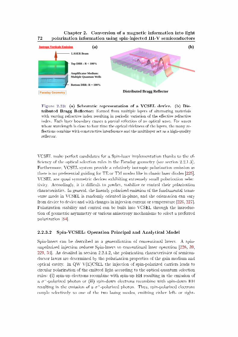
72Chapter 2. Conversion of a magnetic information into light
polarization information using spin-injected III-V semiconductors
Top DBR : R < 100%
Isotrope Verticale Emission
Faraday Geometry
LASER Beam
Bottom DBR: R = 100%
Amplificator Medium:
Multiple Quantum Wells
(a) (b)
Distributed Bragg Reflector
Figure 2.23: (a) Schematic representation of a VCSEL device. (b) Dis-
tributed Bragg Reector: Formed from multiple layers of alternating materials
with varying refractive index resulting in periodic variation of the eective refractive
index. Each layer boundary causes a partial reection of an optical wave. For waves
whose wavelength is close to four time the optical thickness of the layers, the many re-
ections combine with constructive interference and the multilayer act as a high-quality
reector.
VCSEL make perfect candidates for a Spin-laser implementation thanks to the ef-ciency of the optical selection rules in the Faraday geometry (see section 2.2.1.3).Furthermore, VCSEL system provide a relatively isotropic polarization emission asthere is no preferential guiding for TE or TM modes like in classic laser diodes [225].VCSEL are quasi-symmetric devices exhibiting extremely small polarization selec-tivity. Accordingly, it is dicult to predict, stabilize or control their polarizationcharacteristics. In general, the linearly polarized emission of the fundamental trans-verse mode in VCSEL is randomly oriented in-plane, and the orientation can varyfrom device to device and with changes in injection current or temperature [226, 227].Polarization stability and control can be built into VCSEL through the introduc-tion of geometric asymmetry or various anisotropy mechanisms to select a preferredpolarization [84].
2.2.3.2 Spin-VCSEL: Operation Principal and Analytical Model
Spin-lasers can be described as a generalization of conventional lasers. A spin-unpolarized injection reduces Spin-lasers to conventional laser operation [228, 39,229, 34]. As detailed in section 2.2.1.2, the polarization characteristics of semicon-ductor lasers are determined by the polarization properties of the gain medium andoptical cavity. In QW V(E)CSEL the injection of spin-polarized carriers leads tocircular polarization of the emitted light according to the optical quantum selectionrules: (i) spin-up electrons recombine with spin-up HH resulting in the emission ofa σ−-polarized photon or (ii) spin-down electrons recombine with spin-down HHresulting in the emission of a σ+-polarized photon. Thus, spin-polarized electronscouple selectively to one of the two lasing modes, emitting either left- or right-

2.2. From matter to light: Conversion of spin accumulation into lightpolarization information 73
circularly polarized light. Consequently, spin manipulation in a VCSEL provides ameans for optical polarization control. As for Spin-LEDs, the spin-polarized carriersare injected by circularly polarized light or by electrical injection using ferromagneticcontacts. However, contrary to Spin-LEDs, we will show that a purely circularlypolarized emission along with threshold reduction can result under certain bias con-ditions for small spin polarizations.
An intuitive picture depicting the dierences in operation principal between con-ventional and spin polarized lasers was introduced by Zutic et al. using the imageof a bucket lled with water [230]. The bucket model illustrates the changes arisingfrom the injection of spin-polarized carrier in conventional lasers (gure 2.24 (a)):
• Conventional lasers: A simple analogy with the pumped bucket illustratesthe on and o regimes, where the outgoing water represents the emitted light.At low injection or pumping J , the laser operates in a spontaneous emissionregime similar to a LED and the output light generated by the spontaneous re-combination is only negligible. At higher injection, when the injection currentJ reaches the injection threshold JT , the water starts to gush out of the largeslit. For J > JT stimulated emission starts and the emitted light intensity in-creases signicantly. This regime corresponds to lasing operation in which thestimulated recombination is the dominant mechanism of light emission (Figure2.24 (a) 1©). A suciently high injection leads to the onset of lasing whenthe optical gain can overcome losses in the resonant cavity. As the injectionor pumping of the lasers is increased, there is a transition from incoherent tocoherent emitted light that can be described by the Landau theory of second-order phase transitions [230]. In summary, a conventional lasers exhibit twooperating regime (ON and OFF) with one threshold separating the two modesof operation. When pumped with an unpolarized spin current, the gain spec-tra for the left- and right-circularly polarized modes overlap since they are fedwith an equal number of spin-up and spin-down carriers (Figure 2.24 (b) 1©).Consequently, for a perfectly isotropic V(E)CSEL, the emitted-light will belinearly polarized.
• Spin-lasers: To model dierent projections of carriers' spin or helicities oflight, it is convenient to think of an analogy with hot and cold water (Figure2.24 (a) 2©). The bucket is partitioned into two halves, representing two spinpopulations,which are separately lled with hot and cold water, respectively.The openings in the partition allow mixing of hot and cold water, intended tomodel the spin relaxation. With an unequal injection of hot and cold water,injection spin polarization is dened as [230]:
PJ =(J+ − J−)
J(2.38)

74Chapter 2. Conversion of a magnetic information into light
polarization information using spin-injected III-V semiconductors
Cold Hot
Δ
(Spin ↓) (Spin ↑)
σ- σ+
Spin-mixing
(a) Unpolarized
pumping
Leaks
(Spontaneous emission)
(b)
Bucket Model
Gain Spectra
Conventional Laser Spin-Laser
1 2
1 2
Figure 2.24: Comparison of operation principal between Conventional-
Lasers and Spin-Lasers. (a) Lasers bucket model: 1. Conventional Laser:
The water (unpolarized injection) lls the bucket until the threshold is reached and
the water starts to gush out (Stimulated emission). Only two operatin regimes are
displayed: either OFF or ON. 2. Spin-Laser: Two halves of the bucket, representing
two spin populations (hot and cold water) are separately lled. Here, in addition to
the ON and OFF regimes, one can infer a regime where only hot water will gush out.
This represents the spin-ltering regime between two dierent lasing thresholds: even
a modest polarization of injection leads to complete polarization of emission. Figures
adapted from [230]. (b) Gain spectra: 1. Conventional Laser: When pumped
with an equal number of spin-up and spin-down, the gain spectra for σ+- and σ−-
polarized modes overlap. 2. Spin-Laser: If the laser is pumped with a spin-polarized
current, a gain anisotropy favoring the majority carriers immediately appears. Figures
adapted from [84].
where J+ and J− are the injection/pumping of the spin-up and spin-downpopulations respectively which together comprise the total injection/pumpingJ = J+ +J−. Compared to conventional lasers, the spin imbalance ∆ between

2.2. From matter to light: Conversion of spin accumulation into lightpolarization information 75
the spin-up and spin-down populations (dierence in the hot and cold waterlevels) leads to three dierent lasing regimes and two dierent lasing thresholdJT1 and JT2 for the majority and minority spins respectively (Figure 2.25).At low pumping, when the laser is biased below thresholds (both hot and coldwater levels are below the large slit, both circularly polarized lasing modes aresubcritical and only negligible spontaneous emission is produced (Spin-LEDregime). Then, if the pumping increases preferentially for one spin orienta-tion, the associated circularly polarized lasing mode will be fed preferentiallycausing this favored mode to rise above the threshold gain level at the expenseof the other mode, whose peak subsequently falls further below the thresholdgain level. Thus, the spin anisotropy introduced from spin-polarized currentinjection results in a gain anisotropy for the two orthogonal circularly polar-ized lasing modes (Figure 2.24 (b) 2©). Under these pumping conditions, thehot water reaches the large slit and gushes out while the amount of cold watercoming out is still negligible. Such a scenario represents a regime in which themajority spin is lasing, while the minority spin is still in the LED regime. Thusthe stimulated emission exclusively originates from recombination of majorityspin carriers.Two important consequences of this regime are already conrmed experimen-tally:
1. A spin-laser will start lasing for a smaller total injection compared to itsconventional counterpart (only one side of the bucket needs to be lled).This represents the threshold reduction in spin lasers [228, 37, 39, 231,232, 233] which can be parametrized as [230]:
r = 1− JT1
JT(2.39)
with JT1 < JT .
2. Even a modest injection polarization PJ << 1 can lead to highly cir-cularly polarized light [34, 234]. When biased near threshold, a smalldierence in spin polarization can result in a large dierence betweenright- and left-circular polarization intensities if the gain coecient forone mode is above the threshold gain while the other is sub-threshold.The relative width of this "spin-ltering regime" can be expressed as theinterval [229, 230]:
d =JT2 − JT1
JT(2.40)
with JT1 < JT < JT2. The threshold dierence d between the twocircularly polarized mode linked to the two spin-populations increaseswith spin polarization of the injection.

76Chapter 2. Conversion of a magnetic information into light
polarization information using spin-injected III-V semiconductors
Figure 2.25: Photon densities of the left- (S−) and right- (S+) circularly polarized
light as a function of the current density J for a spin-polarization of PJ=0.5 and an
innite electron spin-relaxation time τs → ∞. J is normalized to the unpolarized
threshold current JT = NT
τrwith NT denoting the total electron density at (an above)
threshold. The photon densities S+ and S− are normalized to ST = JTΓτph. The
vertical lines indicate the majority (JT1) and minority (JT2) carrier threholds while
the arrows show their change when PJ decreases. The inset exhibit the total photon
density (S = S+ + S−) for a conventional laser (PJ=0) and two spontaneous-emission
coecients (β=0 and β=0.002), as well as a Spin-laser with PJ=0.5 and β=0. The
theoretical results showcased in this gure were obtained by Gothgen et al. using
a simplied rate equation system deducted from equations (2.42)-(2.44) [39]. Figure
reprinted from [39].
The carrier-photon dynamics of a Spin-V(E)CSEL may be modeled using a spin-dependent rate equation analysis which have already been successfully used to de-scribe both conventional and spin lasers [230, 228, 38, 37, 39, 235, 44, 234, 236,237, 238, 239, 35, 240, 241]. An advantage of this approach is its relative simplic-ity. When simplied according to some experimental conditions, the rate equationscan provide a direct relation between material characteristics and device parame-ters [237]. They also allow to derive analytical solutions [39] and are an eectivemethod to elucidate many trends in the operation of lasers [39, 34].We consider a Multi-Quantum Wells (MQW) structure as the active region of thelaser. The rate equation analysis accounts for the spin-up and spin-down carrierdensities in the barriers n±b , the spin-up and spin-down carrier densities in the ac-tive region n± and the photon density for right- and left-circularly polarized lightS±. The total carrier densities are nb = n+
b + n−b and n = n+ + n−. As the spinrelaxation time of holes is much shorter than the spin relaxation time of electronsτps << τns [162], the holes are here considered unpolarized with p± = p
2 . The to-tal photon density is given by S = S+ + S−. Electrically or optically injectedpumped spin-polarized electrons into the MQW are represented by the current den-

2.2. From matter to light: Conversion of spin accumulation into lightpolarization information 77
sity J = J+ + J− associated with the pump current I. The spin polarization of theelectrically/optically pumped current density is introduced by PJ = (J+−J−)
J as well
as of electron and photon densities Pn = (n+−n−)n and PS = (S+−S−)
S . In the caseof spin-polarized laser, the gain in the laser cavity is generalized as [39, 84]:
g±(n±, S∓) =dg
dn
(n± − ntrans
1− εS∓
)(2.41)
where dndg is the dierential gain, ntrans is the transparency carrier density and
ε is the phenomenological gain compression factor accounting for the non-linearphoton density dependence of the optical gain (g saturates at high photon densitylevels). This gain compression term is an approximate description of the spectralhole burning and carrier heating [39, 242].The system of six coupled rate equations is given by [228, 38, 243, 84]:
∂n±b∂t
= −n±bτcap
+1± PJ
2
I
qVb∓n+b − n
−b
τ barriers
(2.42)
∂n±
∂t=
VbVMQW
∂n±bτcap−υgg±(n±, S∓)S∓∓n
+ − n−
τs−Cn
±(n+ + n−)2
2−Bsp
n±(n+ + n−)
2(2.43)
∂S±
∂t= Γυgg
∓(n∓, S±)S± + ΓβBspn±(n+ + n−)
2− S±
τph(2.44)
where υg is the light group velocity, Γ is the optical connement coecient, βis the spontaneous emission factor and τph is the photon lifetime in the cavity. Bspand C are the bimolecular radiative recombination and Auger recombination coe-cient respectively. The carrier capture time τcap includes the two sequential steps ofcarriers transport from the barriers to the QW and relaxation time within the well.The spin-ip time in the barrier and in the QWs are represented by τ barriers and τsrespectively. Finally, Vb
VMQWstands for the volume ratio between the barriers and
the active region. n±b and n± are normalized with respect to these two volumes.
An example of simulation using these rates equations was proposed by Holub &Bhattacharya to model a AlGaAs/GaAs MQW VCSEL operating at room temper-ature [84]. The results are illustrated in gure 2.26. For a 100% spin-polarized pumpcurrent, the rst simulation clearly highlight that the threshold reduction increasessignicantly when the spin relaxation time ramps up from 10 ps to 2 ns. The sec-ond simulation shows that for a spin relaxation time long enough (τs > 10 ps) the

78Chapter 2. Conversion of a magnetic information into light
polarization information using spin-injected III-V semiconductors
(a) (b)
Figure 2.26: Light vs. Current characteristics of a AlGaAs/GaAs MQW
VCSEL driven with a spin-polarized pump current at room temperature:
(a) Threshold evolution of the majority carriers (JT1) as a function of the spin relax-
ation time τs for a 100% spin-polarized pump current. (b) Threshold current reduction
as a function of the pump spin polarization for dierent spin lifetime. Simulations were
performed using the following parameters: τph = 1 ps, τcap = 20 ps, ntrans = 2 × 10¹⁷
cm−3, dgdn = 7.5 × 10⁻¹⁶ cm2, ε = 1.5 × 10⁻¹⁷ cm3, υg = 0.86 × 1010 cm.s−1, Γ = 0.03,
β = 1.7 × 10⁻⁴, Bsp = 1.0 × 10⁻¹⁰ cm3.s−1 and C = 3.5 × 10⁻³⁰ cm6.s−1. Figures
reprinted from [84].
relative width of this "spin-ltering regime" d (threshold reduction) increases withthe spin-polarization of the pump current. For a τs > 1 ns the threshold reduc-tion approaches the theoretical limit of 50% when the laser is pumped with 100%
spin-polarized pump current.
2.2.3.3 Polarization dynamics of VCSEL: The Spin Flip Model
This section introduces the Spin Flip Model (SFM) developed by San Miguel etal.. The model provides a theoretical understanding of the polarization dynamicsin VCSEL [236]. Compared to conventional edge emitting laser diodes, the lightpolarization of such devices is not well stabilized due to their cylindrical symmetry.This becomes a problem for applications requiring a well stabilized polarizationand numerous solutions were proposed to x or control the polarization state ofthe emitted light. These methods include the introduction of polarization sensitiveDBR [244], geometrical or stress-induced anisotropies [245], or engineering of thesemiconductor material or the growth process [246, 247] to preferentially favor thegain of one polarization. Another paradigm would be to learn how to control and usethe degree of freedom of the polarization vector and use it for applications based onthe control of the polarization state such as optical switching [248, 249], informationprocessing or storage, etc.
Phenomenology of Polarization selection in VCSEL:
The light emitted by VCSEL is typically linearly polarized with the electrical eldvector either: (i) randomly oriented in the (x,y)-plane transverse to the light emis-

2.2. From matter to light: Conversion of spin accumulation into lightpolarization information 79
sion (z-direction) or (ii) with a preferred orientation along one of two orthogonalcrystal axis in the (x,y)-plane. Close to threshold VCSEL generally emits in thefundamental transverse mode. Transverse modes of dierent order are clearly sep-arated in frequency (100-200 GHz) while transverse modes of the same order areseparated in frequency by the birefringence γp in the structure. This separationcan vary from smaller than 1 GHz up to tens of GHz. The birefringence is be-lieved to have two main origins: 1) there is a main and systematic contribution ofthe electro-optic eect during laser operation for electrically pumped VCSEL [250]and 2) a random contribution of the elasto-optic eect [251]. The second contri-bution is due to residual strain in the fabrication process or in the electrical contacts.
Thermal eects are another important aspect inuencing polarization propertiesof VCSEL. The self-heating of the device during operation, mostly induced by theDBR mirrors, leads to a reversible extinction of the output light. For electricallypumped VCSEL, this is explained by the parabolic dependence of the thresholdcurrent with the temperature. The resonant frequency selected by the short opticalcavity and the gain prole red-shift at dierent rates. Consequently, the resonancefrequency is eventually expelled outside the frequencies range for which there is apositive gain. The minimum threshold current corresponds to the alignment of thecavity resonance and the gain peak frequencies. Additionally, the heating of the de-vice can give rise to thermal lensing that produces an eective index guiding eect.
What determines the light polarization state? :
The polarization state of light emitted by a laser depends on two main factors.The rst one is the angular momentum of the quantum states involved in the opticaltransitions (emission or absorption). As explained in the section 2.2.1.2, the emissionof a right- (left-) circularly polarized photon corresponds to an allowed optical tran-sition in which the projection of the total angular momentum of the gain medium onthe direction of light propagation changes by +1 (-1). This mechanism reects thenonlinear dynamics of the gain medium. The second factor is associated with thelinear eects of the laser cavity. The cavity anisotropies (birefringence, dichroism),geometry, detuning and waveguiding eects lead to preferential polarization stateselection. These two ingredients can compete or be complementary to one another.The emitted linear polarization is either randomly oriented in the plane of the activeregion or along two orthogonal directions associated with crystalline orientation. Ifthe gain medium selects linearly polarized light, the birefringence will x the pre-ferred orientations. Then potential polarization switching between these preferredorientations can be explained by phase-amplitude coupling due to the combinedeect of birefringence and detuning. The coexistence of orthogonal polarizations(bistability) and polarization switching can both be observed [226, 252, 227, 253].For conventional edge emitting lasers, cavity eects associated with thegeometry are

80Chapter 2. Conversion of a magnetic information into light
polarization information using spin-injected III-V semiconductors
usually predominant: light is polarized in the plane of the active region since theorthogonal direction displays much larger cavity losses. For VCSEL, the cylindricalsymmetry combined with the isotropy of III-V compounds grown on the [001] di-rection, make the nonlinear gain dynamics much more important. In addition, thesemiconductors linewidth enhancement factor (α) gives the same type of amplitude-phase coupling than detuning in a gas laser, but its magnitude is considerably larger.It is expected that the eect of the saturable dispersion combined with the α-factorand birefringence also plays an important role as a polarization selection mechanism.The α factor of semiconductor lasers [254, 255] is a common way of summarizingin a parameter many microscopic processes and in particular the inhomogeneousbroadened character of the lasing transition. A main eect of the α factor is to pro-duce phase-sensitive dynamics. This sensitivity is analogous to the eect of cavitydetuning in two-level models.
The Spin-ip Model
The Spin-Flip Model (SFM) enables to describe the polarization dynamics of semi-conductor lasers by extending the rate equations model based on a two-level modelapproximation. The rate equations model is not appropriate to describe the po-larization properties of the electric eld on very short time scales. However, theSFM can overcome this limitation as it does not take a x polarization for granted.The SFM is a four level model taking into account the electric eld polarization byincluding the CB and VB spin sub-levels of the semiconductor. Consequently, itallows to consider the light polarization as a degree of freedom of the laser emission.The two distinct carrier densities n↑ and n↓, associated with the spin-up and spin-down populations respectively, cause two lasing transitions associated with right-or left-circularly polarized emission. If there is no disequilibrium between the twotransitions, the two circularly-polarized emissions combined to generate linearly po-larized light. The two transitions are coupled by spin-ip processes characterized
by the so-called spin relaxation rate γsf(
= 1τsf
). The four-level SFM model ac-
counts for the vectorial nature of the light's electric eld by allowing both circularpolarization states through dipole transitions between independent pairs of energylevels [168, 256, 257, 258, 259].
We consider a surface-emitting quantum-well laser with the 2D active mediumoriented perpendicularly to the direction of laser emission (z-axis). The quantizationaxis is also oriented along the z-direction (Figure 2.27 (c)). In this geometry, andfor a gain-guided broad area laser, the electric eld is in the x-y plane, so thattwo independent TE and TM polarization modes are available for the laser eld.The linear components (Ex, Ey) and the circularly (E+, E−) polarized componentssatisfy the relation [236]:
E± =1√2
(Ex ± iEy) (2.45)

2.2. From matter to light: Conversion of spin accumulation into lightpolarization information 81
n1/2
n3/2
n-1/2
n-3/2
(a)
(b)
(c)
γsf
γr γr
Figure 2.27: (a) Schematic band structure of the QW. (b) Schematic representation
of the four level SFM model. (c) Geometry of the surface-emitting laser considered.
A rst important eect of the optical cavity is the selection of a longitudinalmode K with an associated resonant cavity frequency ν. The high reectivity ofeach DBR enable the construction of a vectorial standing wave with a forward andbackward propagating components. In a mean eld approximation, one can averageout the longitudinal z dependence of these amplitudes and write the electric eldfor a single longitudinal laser mode as [236]:
E = [Fx(x, y, t) + Fy(x, y, t)] · exp [ i(K · z − ν · t)] + c.c. (2.46)
where F(x, y, t) is the amplitude of the selected longitudinal mode. FromMaxwell'sequations, one can identify that F originates from the slowly varying amplitude ofthe the dipole polarizations associated with inter-band transitions: P (x, y, t). Thelinear cavity eects amount to a linear cavity susceptibility matrix M . The basicequation for the eld is then:
∂t ~F =ic2
2νn2e
∇2⊥~F + ~P −M ~F (2.47)
where ic2
2νn2e∇2⊥~F represents the diraction in the transverse plane, ne being the
background refraction index. The gain medium polarization ~P and the optical cav-ity contribution M ~F are the two main ingredients contributing to the polarizationselection. The cavity susceptibility M can be written as:

82Chapter 2. Conversion of a magnetic information into light
polarization information using spin-injected III-V semiconductors
M = κI − Γ , with : Γ = −(γa + iγp)
(1 0
0 −1
)(2.48)
where κ is the stimulated emission coecient (⇐⇒ represents the cavity losses),proportional to the stimulated emission cross-section and is the inverse of the photonlifetime. Γ is the cavity anisotropy matrix [260] expressed in the linear basis in thesimplest case where: 1) the circular anisotropies are neglected and 2) the amplitudeand phase anisotropies are along the same directions.
• The hermitian part of Γ is associated with the amplitude anisotropies of theelectric eld components, most commonly named: Dichroism γa. In the cavity,the two orthogonally polarized modes might have a slightly dierent Gain-to-Loss ratio emerging from: (i) the intrinsic gain anisotropies of the crystal [246,262], (ii) a slightly dierent position of the modes frequencies with respectto the gain versus frequency curve [263, 264], and/or (iii) dierent cavitygeometries for the dierently polarized modes [265, 266]. All these potentialeects are regrouped and modeled by the amplitude anisotropy representedby the parameter γa. Experimentally γa is going to select which of the twolinear polarizations has the lower threshold.
• The antihermitian part of Γ is associated with phase anisotropies, also called:Birefringence γp. For VCSEL, it is known that there are often two preferredlinearly-polarized modes that coincide with the crystal axes. These two modeshave a frequency splitting (detunning) associated with the birefringence of themedium. Physically, this linear birefringence γp represents the eect of dier-ent refraction indexes viewed by each polarization modes. An experimentalmeasurement of the mode detuning is a way to quantify the cavity birefrin-gence. γp is typically two orders of magnitude greater than γa [267].
In the VCSEL's QWs, the optical quantum selection rules and the lift of de-generacy between the HH-band and the LH-band in Γ (k = 0) restrain the alloweddipole transitions to CB(-1/2) → HH(-3/2) and CB(1/2) → HH(3/2) associatedwith the emission of right and left circularly polarized light respectively (see section2.2.1.2). In rst approximation, these transitions can be modeled by a four-levelmodel. The picture emerging is a two two-level lasing transitions (two "channels"of light emission) with dierent circular polarizations (Figure 2.27 (b)). The spin-ip mechanism coupling the two spin-sublevels is modelized by the spin-ip rate γsf .
The dynamics of the radiation-matter interaction in the four-level model followsfrom a standard density matrix calculation [268]. This analysis leads to a set ofequations forming with equation (2.47) the closed set of Maxwell-Bloch equations ofthe SFM model. The slowly varying amplitudes (Fx, Fy) satisfy the Maxwell-Blochequations and are conveniently written in terms of right- and left-circularly polar-ized components F± = 1√
2(Fx ± Fy) associated with the transitions CB(-1/2) →

2.2. From matter to light: Conversion of spin accumulation into lightpolarization information 83
HH(-3/2) and CB(1/2)→ HH(3/2) respectively. The four Maxwell-Bloch equationsare given by [236]:
∂tF± = −κF± − ig∗0P± + ic2
2νn2e
∇2⊥F± (2.49)
∂tP± = − [γ⊥ + i(ωg − ν)]P± + ig0F±(D ± d) (2.50)
∂tD = −γr(D − σ) +[ig∗0(F ∗+P+ + F ∗−P−
)+ c.c.
]+Df∇2
⊥D (2.51)
∂td = −γsd+[ig∗0(F ∗+P+ − F ∗−P−
)+ c.c.
]+Df∇2
⊥d (2.52)
where ωg is the band gap frequency, g0 the coupling constant, σ is an incoherentpumping parameter associated with the injection current, Df a carrier diusioncoecient and γ⊥ is the decay rate of the dipole polarization. The model alsoincludes a transverse diraction term and carrier diusion [∇⊥ = (∂x, ∂y)]. Theseequations are written for the two circularly polarized components of ~F and ~P whichnaturally correspond to each of the two coupled two-level systems (Figure 2.27 (b)).The population dierences D and d are dened as [236]:
D =1
2
[(n1/2 + n−1/2)− (n3/2 + n−3/2)
](2.53)
d =1
2
[(n−1/2 − n−3/2)− (n1/2 + n3/2)
](2.54)
where ni/2 stands for the spin population on the sublevel i. Each componentof the material polarization P± is directly coupled to the carrier density D± of thecorresponding two-level system with a dierential gain parameter a. Physically,D = D+ +D− associated with the total population dierence between the CB andthe VB represents the total carrier density referred to its transparency value D0.d = D+ − D− represents the dierence in population inversions associated withσ+- and σ−-polarized emissions. The coupling between the two lasing transitionsoccurs through nonzero values of d. Decay rates are also included to characterize theevolution the two populations dierences D and d. The population dierence D has
an associated decay rate γr(
= 1τr
)accounting for the electron-hole recombination
while the decay rate associated with d is dened by [236]:

84Chapter 2. Conversion of a magnetic information into light
polarization information using spin-injected III-V semiconductors
γs = γr + 2γsf (2.55)
The phenomenological constant γs(
= 1τs
)is introduced to model spin-ip in
the CB and the VB and take into account the spin relaxation processes mixing thecarriers population with opposite Jz values. In QWs, experimental measurementsof spin relaxation times have estimated that [259, 269, 236]:
γr ≤ γsf ≤ 102 · γr ⇐⇒ 10−2 · τr ≤ τsf ≤ τr (2.56)
with 1γr
= τr ≈ 1 ns. Typically for monolithic VCSEL, the spin mixing occurs on
larger time scales than the photon lifetime: τp(= 1
κ
)≈ 1 ns τsf ∈ [10ps − 1ns].
Case of a single mode emission
For fundamental understandings, we treat here the most simple case of a VCSELoperating on the fundamental transverse mode with two polarization modes shiftedin frequency.
Equations (2.49) to (2.52) can be simplied when the reasoning is restricted tothe polarization dynamics of a single longitudinal mode with neglected transverseeects. The fastest time scale included in equations (2.49)-(2.52) is the decay rateof the dipole polarization: γ⊥ γr, γs, κ. Therefore, in time scales relevant toVCSEL operation, the dipole polarization variables (~P ) follows the dynamics of theother variables and can thus be adiabatically eliminated. Note however, that dtypically evolves in an intermediate dynamical scale between D and F±. Withinthis model, it plays a crucial role in the nonlinear dynamical properties of the VC-SEL. The elimination of P denes, through equation (2.50), a susceptibility matrixχ± [236]:
P± = χ± · F± =g0(Ω + iγ⊥)
Ω2 + γ2⊥
(D ± d) · F± (2.57)
where Ω = ωg − ν stands for the detuning parameter which characterize thedierence between the mode frequency (= band gap frequency) ωg and the cavityresonant frequency ν. The linewidth enhancement factor of the semiconductors laserα (normalized detuning) can be expressed as a function of the susceptibility matrixχ±:
α =Re(χ±)
Im(χ±)=
Ω
γ⊥=ωg − νγ⊥
(2.58)

2.2. From matter to light: Conversion of spin accumulation into lightpolarization information 85
A reduction of equations (2.49)-(2.52) with an apropriate choice of unit so that:E± ∼ F±, N ∼ (D − D0), n ∼ d, lead to the following Maxwell-Bloch equationsystem [270]:
dE±dt
= −κE± − iω0E± + κ(1 + iα)(N ± n)E± (2.59)
dN
dt= −γr(N − µ)− γr(N + n)|E+|2 − γr(N − n)|E−|2 (2.60)
dn
dt= −γsn− γr(N + n)|E+|2 + γr(N − n)|E−|2 (2.61)
This equation system describes a VCSEL operating in the fundamental trans-verse mode with two polarization modes with dierent frequencies. N = N+ +N−represents the total population inversion (total carrier number in excess of its valueat transparency normalized to the value of that excess at the lasing threshold) whereN+ and N− are the population inversion for the transition amplifying σ+- and σ−-polarized light respectively. n = N+ −N− is the population inversion between thetransitions between the magnetic sublevelss, i. e. the dierence between the popula-tion inversions for the σ+ and σ− transitions. We also dene N0 as the unsaturatedpopulation inversion proportional to the pumping rate. N , n and N0 are dimen-sionless quantities, i. e. numbers of atoms or dierences between numbers of atomson the dierent levels [271].
In this model, the spin ip rate γs has to be considered as an eective parameterdescribing a variety of microscopic processes. In a VCSEL in operating conditionsthere is a dense plasma of electron and holes with no signicant exciton contribution.Since holes in QWs are known to relax much faster than electrons, the importantspin relaxation processes are those of the electrons at RT. The spin lifetime is foundto be a non-monotonic function of carrier density. For a lower n-doping level of bulkGaAs semiconductor materials, lifetimes larger than 100 ns have been observed ata temperature of 5 K [75]. These lifetimes are far longer than the electron-holerelaxation time and in these cases the spin lifetime becomes the slow time scale ofthe system.
In an operating VCSEL, very little is known about the relative importance of thedierent spin relaxation mechanisms and the spin relaxation time of the electronsunder the high-density, room temperature conditions. However, some proposals andexperiments have been made to determine γs (τs) on the basis of the SFM modelintroduced above. One is based on measuring the eect of a longitudinal magneticeld on the emitted light ellipticity due to the Zeeman splitting of the magnetic

86Chapter 2. Conversion of a magnetic information into light
polarization information using spin-injected III-V semiconductors
sublevels [272, 273]. Another technique is based on tting the values of injectioncurrent associated with polarization switches at constant temperature [274, 275].Other measurements [276] are based on the uctuations of the ellipticity and thepolarization direction as well as on properties of the optical spectrum [277, 278]. Anal proposal is based on the analog of the Hanle eect for an optically pumpedVCSEL [267]. These studies give an estimation of the characteristic spin relaxationtime in the range of 1-15 ps. Given the fact that they are indirect measurements,the actual value of the electron spin relaxation time and of the eective parameterγs (τs) determined from them is rather uncertain. However, it will be seen thatpolarization selection and switching is very sensitive to its precise value. Generally,one should remember that an excess in the decay rate γs over γr accounts for themixing of the carriers with opposite value of Jz.
The predictions of this limit case concerning polarization selection and polariza-tion switching are summarized in further [270]. As compared with the most generalequations (2.49)-(2.52), these equations do not contain a frequency dependent gainand dispersion as there values are xed by the single operating frequency of the laser.Consequently, the two polarization modes splitted in frequency by the birefringenceγp are seeing the same gain. However, small dierences in gain associated with thebirefringence can be taken into account through an amplitude anisotropy parameterγa. While in (2.49)-(2.52) this parameter only models intrinsic cavity anisotropies,it can be used in this particular case to account for the gain dierences. It can alsoeventually depends on the injection current and/or the temperature.
Incorporating the linear phase anisotropy γp (birefringence) and the amplitudeanisotropy γa into equation (2.52) leads to:
dE±dt
= κ(1 + iα)(N ± n− 1)E± − iγpE∓ − γaE∓ (2.62)
The model given either by the set of equations (2.49)-(2.52) or the set (2.59)-(2.61) includes ve fundamental physical processes shown to control the polarizationstate to a large extent: the Henry phase-amplitude coupling factor α [254], the linearamplitude anisotropy γa, the linear birefringence γp, the total e− - h+ recombina-tion rate γr and spin relaxation rate γs. The inuence of these parameters can behighlighted when rewriting the equations (2.59)-(2.61) in terms of the orthogonallinear components of the electric eld: Ex = 1√
2(E+ + E−), Ey = i√
2(E+ − E−) .
The system becomes [270]:
dExdt
= −(κ+ γa)Ex − i(ω0 + γp)Ex + κ(1 + iα)(NEx + inEy)
dEydt
= −(κ− γa)Ey − i(ω0 − γp)Ey + κ(1 + iα)(NEy + inEx)
(2.63)

2.2. From matter to light: Conversion of spin accumulation into lightpolarization information 87
dN
dt= −γr
[N(1 + |Ex|2 + |Ex|2
)− µ+ in
(EyE
∗x − ExE∗y
)](2.64)
dn
dt= −γsn− γr
[n(|Ex|2 + |Ex|2
)+ iN
(EyE
∗x − ExE∗y
)](2.65)
where ω0 = κα is a frequency shift and µ is the normalized injection current(µ=1 at threshold). We see from the set of equation (2.63)-(2.65) that the lin-ear birefringence γp induce a frequency detuning of 2γp between the x- and they-polarized solutions (with ωx < ωy when γp > 0). The linear dichroism γa leads todierent thresholds for the two linearly polarized solutions (µxth < µyth when γa > 0).Note that the values of linear birefringence and the linear dichroism strongly dependon the VCSEL design. The eigenstates of the system are linearly polarized (ratherthan circularly or elliptically polarized) because of the cross-saturation preferenceexerted through the nontrivial value of γs [270]. In the absence of saturable dis-persion (α = 0) and/or birefringence (γp = 0), the dichroism γa fully controls thestability of the two modes. In this case, the mode with the higher Gain-to-Loss ratio(lower threshold) is always stable above threshold and the orthogonally polarizedmode is always unstable when the solution exists (above a higher threshold valueof the current). Then a polarization switch can only occurs for a sign change ofγa [270].
Basic polarization states:The rate equations (2.59)-(2.61) admit CW solutions above threshold that cor-
responds to linearly polarized light and can be generally written as [270]:
E± = Q± · exp [i(ω±t± ψ) + iθ] , N = N0, n = n0 (2.66)
where θ is the global arbitrary laser phase and ψ the relative phase. Solutionswith a well dened polarization are those with a single frequency (ω+ = ω−). Cir-cularly polarized solutions are those in which either Q+ = 0 or Q− = 0. Linearlypolarized solutions are those with Q+ = Q−. For these solutions the angle ψ givesthe orientation of the linearly polarized light in the (x,y)-plane. Ellipticaly polarizedsolutions are those in which the two real amplitudes Q± are nonzero and dierent.The ellipticity of these solutions is given by ε = Q+−Q−
Q++Q−. Starting from these ex-
pressions for the electric eld's circularly polarized components, we are going todistinguish dierent situation depending on the values of the linear birefringence γpand the linear dichroism γa [270]. The detailed solutions with the associated electriceld projections in the (x,y)-basis can be found in the Appendix 2.

88Chapter 2. Conversion of a magnetic information into light
polarization information using spin-injected III-V semiconductors
A) If α 6= 0, γa 6= 0 and γp 6= 0 : In the most general case, the system admitstwo orthogonal linearly polarized solutions along the x- and the y-axis. Thesetwo states have dierent amplitudes and dierent threshold values µth = N0
due to the amplitude anisotropy γa. This anisotropy also causes that thefrequency dierence ωx - ωy between the two modes does not coincide withthe birefringence induced splitting 2γp.
B) If α 6= 0 and γa = γp = 0 : If the VCSEL is perfectly isotropic the solutions(2.66) are linearly polarized with equal frequencies and amplitudes for thetwo circularly polarized components. Here, the relative phase ψ is arbitraryand xes the orientation of the linear polarizations in the (x,y)-plane. Thisunique linearly stable solution is susceptible to orientational diusion in the(x,y)-plane due to perturbations of the phase ψ. Nevertheless, when γs →∞(τs → 0) the mode becomes marginally stable with respect to the amplitudesuctuations. This means that for a perfectly anisotropic VCSEL a long spinlifetime paradoxally stabilizes the linearly polarized emission and destabilizescircularly polarized or elliptically polarized emission [236, 270].
C) If α 6= 0, γa = 0 and γp 6= 0: In absence of dichroism the system displays fourdierent steady states solutions (Figure 2.28 (a)). For each of these solutions,the birefringence γp breaks the rotational invariance of the polarization vector:the relative phase is no longer arbitrary (ψ 6= 0). Two of these solutions areorthogonal and linearly polarized (circularly polarized components with equalamplitudes) along x- and y-direction respectively (Figure 2.28 (a) 1©- 2©) whilethe other two solutions are elliptically polarized (circularly polarized compo-nents with unequal amplitudes) (Figure 2.28 (a) 3©- 4©). In the particular casewhere γs = 0 each elliptically polarized solution becomes circularly polarizedlight, however these circularly-polarized states are never found to be stablesolutions of (2.63)-(2.65) [236].
Stability analysis:
We introduce here the main qualitative conclusion of the analysis conducted byMartin-Regalado et al. concerning basic polarization modes stability. For quantita-tive precisions I invite the reader to refer to their paper [270]. This study describesthe growth or decay of small uctuation around the polarization states and identiesthe relevant parameters and mechanisms which control polarization selection andswitching. The eigenvalues found in such a linear analysis determine the stabilityboundaries of the dierent polarization states:
• The stability of linearly polarized mode can be separated in two indepen-dent problems. The rst one refers to the total laser intensity uctuationsI = |E+|2 + |E−|2 and the total carrier number N0. It is independent of thedichroism γa, the birefringence γp and the spin relaxation rate γs in the sys-tem. The second problem concerns the polarization dynamics properties and

2.2. From matter to light: Conversion of spin accumulation into lightpolarization information 89
(b)
Birefringence γp
No
rma
lize
d i
nje
ctio
n c
urr
ent μ
(a)
0
0
0
0
0 0
0 0
Re (Ex)
Re (Ey)
Re (Ex)
Re (Ey)
Re (Ex)
Re (Ey)
Re (Ex)
Re (Ey)
1 2
3 4
Figure 2.28: (a) Steady-state solutions of (2.63)-(2.65) in the case where
α 6= 0, γa = 0 and γp 6= 0: 1. x-polarized solution, 2. y-polarized solution and
3-4. elliptically polarized. (b) Stability diagram for the steady-state solutions:
The x-polarized state is stable below the continuous line, while the y-polarized state is
stable to the left of the dashed line. The graph is divided into four areas with dierent
stability for the two linearly polarized solutions: in I, both solutions are stable; In II,
neither solution are stable; in III, only the x-polarized solution is stable and in IV,
only the y-polarized solution is stable. Elliptically polarized solutions are stable within
the narrow region between the solid line and the stars. The following parameters have
been used to perform the simulation: κ = 300 ns−1, γr = 1 ns−1, γs = 50 ns−1 and α
= 3. Figures reprinted from [270].
is linked to the dierence in carrier populations with dierent spin numbern0. It is also equivalently linked to the coupled uctuations of the polariza-tion direction ψ, the ellipticity and the carrier populations with dierent spinnumber n0.
• Inspection of the characteristic equation that determines the stability of lin-early polarized states reveals the importance of dierent parameters. For aperfectly isotropic VCSEL (γa = γp = 0, with α 6= 0) there is a vanishingeigenvalue associated with the arbitrary orientation of the linearly polarizedstate. For an anisotropic VCSEL there is three possible situation dependingon the parameters domains in which either only one, both (bistability) or noneof the linearly polarized states are stable (Figures 2.28 (b)). When there isno birefringence (γp = 0) only one of the two linearly polarized solutions isstable. In the case where α = 0 and γa = 0, the VCSEL is bistable and bothpolarization modes can coexist. This is still true for reasonably small values ofγa except for extremely large or small birefringence γp. For α = 0 and typicalvalues of the other parameters (γa, γp, γs 6= 0), whichever state is selected atthreshold (lower threshold due to the dichroism γa) will always remain sta-ble. A change in the relative stability of the two linearly polarized modes isthus due to the combined eect of birefringence γp and saturable dispersion

90Chapter 2. Conversion of a magnetic information into light
polarization information using spin-injected III-V semiconductors
α. Likewise, in the limit of innitely fast spin relaxation (τs = 0) there isagain only bistability. A nite spin relaxation time is a necessary conditionfor stability changes and polarization switching.
• In the domain of parameters where a linearly polarized mode is stable itsoptical spectrum shows two qualitatively dierent regimes. For a symmet-ricl VCSEL (γp = 0) with small dichroism values (γa ≈ 0), two regimes canbe distinguished depending on the spin relaxation rate γs: 1) a fast spin re-laxation regime with exponential uctuations relaxation and 2) a slow spinrelaxation regime exhibiting damped polarization relaxation oscillations [236].The ellipticity ε and the carrier populations with dierent spin n0 oscillate ata frequency comparable to the laser relaxation oscillations frequency. The tworegimes are separated by a critical value of the spin relaxation rate γs com-parable to the frequency of the relaxation oscillations. For a non vanishingbirefringence (γp 6= 0), the slow spin relaxation regime is continued into one"polarization relaxation oscillations" persisting far above threshold while thepolarization direction uctuations (xed by γp) relax exponentially. However,close to threshold, in the case of fast spin relaxation, a new regime appearswhere n0 relaxes exponentially (characteristic time τs) while damped coupledoscillations of the ellipticity ε and the polarization orientation ψ emerge. Theseoscillations occur at a frequency growing linearly with the threshold distanceand are thus dierent from the relaxation oscillation frequency that evolve asthe square root of the threshold distance. Most generally, VCSELs operate inthis fast spin relaxation regime but note however that relatively small varia-tions of the injection current and/or spin-ip rate can lead to a switch from aregime to another.
• A better understanding of the spin-dynamics inuence on the VCSEL behav-ior is obtained when considering equations (2.63)-(2.65) in the limit where n= 0. In the limit of extremely fast spin relaxation (τs → 0), there is no pref-erential stabilization between linearly- or circularly-polarized modes. From amathematical viewpoint, it can be identied using a 3rd-order Lamb expres-sion obtained from (2.63)-(2.65) by adiabatic elimination of N and n whenlim γs, γr → +∞ [270]:
∂E±∂t
= −(γa + iγp)E∓ · κ(1 + iα)
(µ+
µ
ρ
)[µ− 1
µ+ µρ
− |E±|2 − δ|E∓|2]E±
(2.67)
where δ = ρ−1ρ+1 denes the coupling parameter with ρ = γs
γr. Then, in the case
of a weak coupling (δ < 1) linearly polarized mode will be dominant, while fora strong coupling (δ > 1) a stable circularly polarized emission is predicted.

2.2. From matter to light: Conversion of spin accumulation into lightpolarization information 91
Polarization switching:
Polarization switching can occur when one of the two linearly polarized states loosesstability. For a xed value of α the analysis can be conduct for two parameters com-monly measured in polarization switching experiments: the injection current µ (oroptical injection power density) normalized to the threshold current and the bire-fringence γp. One can note that the intrinsic birefringence is a xed characteristicof a given VCSEL structure and is independent of the injected current. Neverthe-less a pumping induced birefringence also inuence the dynamical behavior of thedevice (Thermal eects). For a constant α, the switching of polarization modes iscontrolled by the relative values of the birefringence γp and the spin-ip rate γsthrough γcritp = γs
2α . In each case a dierent polarization state is selected at thresh-old. In both cases elliptically polarized states are only stable in a narrow range ofparameters as intermediate states between stable modes transition:
A) γa > 0 (µxth > µyth): The gain dierence favors the y-polarized mode atthreshold so that the threshold for the x-polarized mode is higher than for they-polarized mode.
• If γp < γs2α : For a low birefringence VCSEL, the mode with the lower
threshold (here y-polarized mode) is selected at threshold and remainsstable as the pumping power increases.
• If γp >γs2α : an abrupt y→ x switching occurs when increasing the injected
current. The switching occurs by destabilization of the mode with thehigher gain-to-loss ratio in favor of the weaker mode. In addition, theswitching threshold µsw linearly depends on the dichroism γa:
µswµyth
= 1 +2(γ2s + 4γ2
p
)κ (2αγp − γs)
γaγe
(2.68)
When decreasing the pumping power, the reverse switching x→ y occurswith a potential hysteresis in the switching threshold.
B) γa < 0 (µxth < µyth): The gain dierence favors the x-polarized mode atthreshold so that the threshold for the y-polarized mode is higher than for they-polarized mode. In this case, stable x-polarized emission is expected closeabove threshold for any birefringence value.
• If γp <γs2α : x → y polarization switching occurs when the injection cur-
rent is increased and happens again from the higher gain mode to thelower gain mode with higher threshold. The switching is not abrupt andoccurs through one of the two stable elliptically-polarized states with de-generate frequencies. Consequently, elliptically polarized modes appear

92Chapter 2. Conversion of a magnetic information into light
polarization information using spin-injected III-V semiconductors
as intermediate states reached in the destabilization of the linearly po-larized solution as the pumping is increased. Hysteresis in the switchingcurrent, is also predicted here. The switching threshold is given by:
µswµxth
= 1 +
(γ2p + γ2
a
)κ (2αγa + αγp)− γ2
p
γsγe
(2.69)
• If γp > γs2α : the x-polarized mode is selected at threshold and remains
stable as the pumping power increases.
The above discussion clearly highlights the role of α, γp and γs in determiningthe stability properties of the dierent polarization states. According to the expres-sions of the switching thresholds (2.68) and (2.69), one can conclude that the basicmechanisms inducing a polarization switching in a VCSEL structure are: 1) the cou-pling through spin-ip processes (γs) of the two carrier populations with dierentspin number and 2) the combined eect of birefringence γp (which couples the twocircularly polarized components of the eld) with the dichroism (with associatedsaturable dispersion α).
Specic case of Optically Pumped VCSEL/VECSEL:
So far we considered V(E)CSEL modeled as a two two-level systems assuming thatthe two transitions associated with the two spin-orientations are pumped with equalstrength. However, optically pumping the VCSEL with an o-resonance eld allowsto selectively favor one of the two lasing transitions by changing the pump elliptic-ity. For a non-linearly polarized pumping, a non-zero macroscopic magnetizationmz ∼ n is induced by generation of carriers with a preferred spin orientation. Doingso, the inuence of the spin dynamics on the device behavior is amplied and spinrelated eects become more apparent. Optically pumped V(E)CSEL are thus veryuseful for fundamental studies of polarization selection mechanisms and other moregeneral dynamics properties. Additionally, optical pumping with moderate powerdensities can avoid to a large extent temperature eects mostly due to the self-heating of the electrical devices. Finally, under optical pumping V(E)CSEL exhibita more eective coupling between the two lasing transitions associated with rightand left circularly polarized light. This property is quite interesting for developingpotential application based on self-sustained polarization oscillations.For a V(E)CSEL operating in the fundamental transverse mode the optical pump-ing is modelized by simply replacing the electrical pumping variable µ in the rateequation (2.63)-(2.65) by η+ and η− such that [279]:
2.2. From matter to light: Conversion of spin accumulation into lightpolarization information 93
dExdt
= −(κ+ γa)Ex − i(ω0 + γp)Ex + κ(1 + iα)(NEx + inEy)
dEydt
= −(κ− γa)Ey − i(ω0 − γp)Ey + κ(1 + iα)(NEy + inEx)
(2.70)
dN
dt= −γr
[N(1 + |Ex|2 + |Ex|2
)− (η+ + η−) + in
(EyE
∗x − ExE∗y
)](2.71)
dn
dt= −γsn− γr
[(η+ − η−) + n
(|Ex|2 + |Ex|2
)+ iN
(EyE
∗x − ExE∗y
)](2.72)
where η+ and η− are the pumping eciencies for the HH(-3/2)→CB(-1/2) (E+)and HH(3/2)→CB(1/2) (E−) transitions respectively. The pump ellipticity is thengiven by P optpump = η+−η−
η++η−. As for Spin-LEDs, informations on the carriers and spin
dynamics in the structure can then be deducted from studying the output laser lightellipticity as a function of P.
2.2.3.4 Interest, Stakes and Applications
Spin-Lasers provide higher performances as compared to Spin-LEDs in terms of out-put Degree of Circular Polarization (DoCP) due to the amplication eect inducedby the combination of a gain medium and a resonant optical cavity. An output DoCPclose to 100% can hence be achieved even by injecting a relatively low polarizedspin-current in the active medium. From this viewpoint, the device can be seen asa spin-amplier [224]. Such Spin-Lasers would provide a number of advantages overconventional VCSELs for future optical communication systems such as telecom-munications with enhanced bandwidth, spin driven recongurable optical intercon-nects [31, 32, 33], fast modulation dynamics [34, 35], polarization control [36, 37] aswell as higher performances such as laser threshold reduction [37, 38, 39], improvedlaser intensity, and polarization stability. The ideas emerging from Spin-Lasers andpolarization switching may also motivate other device concepts such as, for example,cryptography, coherent detection systems or magneto-optical recording [40]. Sinceelectron spin is intricately linked to photon polarization, control and manipulationof electron spin provides a means for polarization control in a laser [84].
Recent experimental advances in the dynamics operation of Spin-Lasers were alsohighlighted [234, 35]. In dynamic operation, Spin-Lasers are expected to outper-form the conventional counterparts in two key categories: the bandwidth modula-tion and the frequency chirp [280, 34]. In Spin-Lasers there are two basic methodsof modulation: amplitude modulation and polarization modulation. While ampli-tude modulation modies the injection intensity, polarization modulation modiesthe light polarization at a xed injection intensity [281]. In both cases, bandwidths(the range where the frequency response is above -3dB) are enhanced with increasedpolarization (see [34]).

94Chapter 2. Conversion of a magnetic information into light
polarization information using spin-injected III-V semiconductors
2.2.3.5 State-of-the-art
Optical Spin Injection
The very rst demonstration of polarization modulation in VCSEL was achievedby Hallstein et al. [282]. The philosophy of the experiment was to applied a strongtransverse magnetic eld on the structure to modulate the spin orientation of the in-jected carrier through Larmor precession. The VCSEL was pumped by unpolarizedlight in a pulsed regime. They observed an output stimulated emission with alter-nating circular polarization synchronized with the Larmor frequency of the electrons.
Strictly speaking, the rst demonstration of spin-injection in a VCSEL using circu-larly polarized optical pumping was performed by Ando et al. reaching a DoCP of75% at room temperature [36]. This rst successful experiment already overpow-ered the best results obtained with Spin-LEDs up to this day and highlighted theattractiveness of such spin-injected devices for potential applications.
Rudolph et al. then focused on another interesting property of spin-injected VCSEL.They observed threshold reduction at both low and room temperature in InGaAsQWs and GaAs QWs structures under circularly polarized optical pumping [228, 38].They also introduced the rst rate equation model describing the carrier-photon dy-namics of a Spin-V(E)CSEL (section 2.2.3.2).
Pumping Active Region λ Spin Polarization (%) Reference
emission / Temperature (K)
Pulsed 2× InGaAs QWs 835 nm N.C./15 K [282]
Pulsed GaAs bulk 865 nm 75%/300 K [36]
Pulsed 2× InGaAs QWs 835 nm N.C.%/6 K [228]
Pulsed 3× GaAs QWs 850 nm N.C.%/294 K [38]
Pulsed 2× InGaAs QWs 1000 nm 100%/300 K [41]
Pulsed 5× (110)-InGaAs QWs 865 nm77 K 94%/77 K [283]
917 nm300 K 42%/300 K [283]
Pulsed 3× (110)-GaAs QWs 855 nm 96%/300 K [42]
Pulsed N.C. 853 nm 35%/300 K [284]
CW 15× GaInNAs QWs 1300 nm 73%/300 K [43]
CW 12× InGaAs QWs 1000 nm 80%/300 K [225]
Mixed 3× GaAs QWs 830 nm 100%/300 K [224]
Table 2.6: Comparison of state-of-the-art optical spin injection in V(E)CSEL with
dierent active mediums and architectures. For each type of pumping, the refrences
are historically displayed.
2.2. From matter to light: Conversion of spin accumulation into lightpolarization information 95
Gerhardt et al. conrmed the amplication of the spin-information expected inSpin-VCSEL. They achieved a DoCP of 100% with a carrier spin-polarization of30% and showed that a carrier spin-polarization of 13% still provide a DoCP of50%. These results are also in good agreement with the theoretical calculationsbased on the SFM mentioned in section 2.2.3.2 [41].
More recently, Fujino et al. and Iba et al. stepped up the performances of Spin-VCSEL using (110)-oriented QWs. In (110)-QWs the Dyakonov-Perel relaxationmechanism is canceled inducing a signicantly longer spin life-time compare to themore conventional (100)-QWs. They respectively reached DoCP of 94% at 77K [283]and 96% at 300K [42] under pulsed circularly polarized optical pumping.
Spin injection under mixed electrical/optical pumping has also been demonstratedby Hovel et al. with an output DoCP of 100% [224]. The industrial VCSEL waspumped with a xed unpolarized electrical current corresponding to 80% of the elec-trical threshold. Then, the control the VCSEL polarization through spin-injectionby further adding a CW circularly polarized optical pumping to pass the lasingthreshold.
Finally, during this Ph.D we reported the rst demonstration of optical spin in-jection in a Vertical-External-Cavity-Surface-Emitting-Laser reaching a DoCP of80% at room temperature [225]. Table 2.6 overviews the state-of-the-art of spininjection in V(E)CSEL using circularly-polarized optical pumping.
Electrical Spin Injection
To this day, electrical spin-injection in VCSEL has exclusively been investigatedby the group of P. Bhattacharya from the Department of Electrical and ComputerEngineering of University of Michigan. Their work regroups a total of 4 publishedpapers on the subject. Dierent structures with dierent active mediums and dif-ferent spin-injectors have been implemented. A maximum DoCP of 15% at 200 Kfor an applied magnetic eld ~B of 2 T was reached using an MnAs Schottky injectoron InAs/GaAs QDs [44]. Unfortunately, as the intrinsic magnetization of all thespin-injectors used was in-plane, an applied magnetic eld was needed to drag thelayer's magnetization out-of-plane and polarized the carriers to fulll the opticalquantum selection rules in the Faraday geometry. As for Spin-LEDs, this standsout as a limitation for potential applications. This problem can be solved by theuse of a ferromagnetic spin-injector displaying Perpendicular Magnetic Anisotropy.
Architecturally, despite for the rst device [285], the spin-injection is achieved later-ally by injection through the n-doped bottom DBR thanks to an annular electrode.Questions rises concerning the conservation of the spin-polarization through thisstack of alternating materials over an almost micrometric distance.

96Chapter 2. Conversion of a magnetic information into light
polarization information using spin-injected III-V semiconductors
Spin Injector Active Region λ Spin Polarization (%) Reference
DMS|FM emission /Temperature (K)/ ~B (T)
GaMnAs 5× InGaAs QWs 945 nm 4.6%/80 K/1 T [285]
Fe 3× InGaAs Qws 948 nm 23%/50 K/2 T [37]
MnAs 10× (InAs/GaAs QDs) 983 nm 8%/200 K/3 T [235]
MnAs InAs/GaAs QDs 983 nm 15%/200 K/2 T [44]
Table 2.7: Comparison of state-of-the-art electrical spin injection in VCSELs with
dierent active mediums and architectures. The references are historically displayed.
To this day, an ecient electrical spin injection in VCSEL without any appliedmagnetic eld remains to be seen, even at low temperature. This stands out asa tremendous technological challenge involving expertise in semiconductors, optics,spintronics, growth and characterization techniques as well as ferromagnetic thinlm engineering. Table 3.7 overviews the state-of-the-art of spin injection in VC-SEL using spin-polarized electrical pumping.

Chapter 3
Development and optimization of
an ultra-thin MgO/CoFeB/Ta
spin-injector with perpendicular
magnetization.
Contents
3.1 Spin-LEDs structures and Photolithography process . . . . 99
3.1.1 Spin-LEDs structures . . . . . . . . . . . . . . . . . . . . . . 99
3.1.2 Sample preparation . . . . . . . . . . . . . . . . . . . . . . . 100
3.2 Optimization of the MgO Tunnel Barrier: MBE vs. Sput-
tering growth . . . . . . . . . . . . . . . . . . . . . . . . . . . . 102
3.2.1 Samples preparation . . . . . . . . . . . . . . . . . . . . . . . 102
3.2.2 Impact of annealing on the MgO/CoFeB bi-layer . . . . . . . 103
3.2.3 Role of the GaAs/MgO and MgO/CoFeB interfaces . . . . . 108
3.3 Development of an ultra-thin MgO/CoFeB spin-injector
with Perpendicular Magnetic Anisotropy . . . . . . . . . . . 112
3.3.1 Physical origins of Perpendicular Magnetic Anisotropy in ultrathin-
ferromagnetic-lms . . . . . . . . . . . . . . . . . . . . . . . . 112
3.3.2 Sample preparation and structural characterization . . . . . . 118
3.3.3 Magnetic properties of the spin-injector . . . . . . . . . . . . 120
3.3.4 Perpendicular Magnetic Anisotropy of MgO/CoFeB bi-layer . 121
3.3.5 Measurements and characterization . . . . . . . . . . . . . . . 123
3.4 Limits and Perspectives . . . . . . . . . . . . . . . . . . . . . 132
Introduction
Since the discovery of an ecient transfer of a solid-state information stored withinferromagnetic materials into circularly polarized photons emitted by spin-light emit-ting diode (spin-LED) [29, 197, 286], several advanced semiconductor technologieshave been proposed. Potential devices have been anticipated ranging from memory
98Chapter 3. Development and optimization of an ultra-thin
MgO/CoFeB/Ta spin-injector with perpendicular magnetization.
elements with optical readout and optical transport of spin information [287], ad-vanced optical switches [84], circularly polarized single photon emitters for quantumcryptography [288] to chiral analysis [289] and 3-dimensional display screens.
According to the optical selection rules [168, 290], conventional spin-injector within-plane magnetization [204, 123, 91, 93, 22, 99] cannot satisfy the practical ap-plication for quantum well (QW)-based spin-LEDs. Indeed, with these injectors astrong external magnetic eld up to a few Tesla is required to rotate the injector'smagnetization out-of-plane. Moreover, the ecient injection of spin-polarized elec-trons from a ferromagnetic (F ) contact into a semiconducting heterostructure (SC)is a prerequisite for the realization of functional spin-optoelectronic devices. It hasbeen shown that inserting a thin MgO tunnel barrier in-between F and SC cancircumvent the impedance mismatch issue arising when a metals is put in contactwith a semiconductors (section 2.1.1.4). The SC/MgO/F architecture has alreadydemonstrated very high spin-injection eciencies [63]. In particular, MgO/CoFeBinjectors exhibited the highest spin-injection yield at room temperature. After depo-sition on a n-i-p LED structure, an emitted Degree of Circular Polarization (DoCP)of 32% was reached at room temperature. To this day, this value remains the worldrecord for circularly-polarized emission using a Spin-LED device [99].
This third chapter focuses on the development and the optimization of a new ultra-thin MgO/CoFeB/Ta spin-injector exhibiting Perpendicular Magnetic Anisotropyon semiconductor Spin-LED. We detail the device structures and their fabrica-tion by photolithography processing. In the second section we focus on the op-timization of the MgO tunnel barrier for maximizing the spin-injection eciency.The third section is fully devoted the development and the characterization of aMgO(2.5nm)/CoFeB(1.2nm)/Ta(5nm) spin-injector with perpendicular magnetiza-tion at remanence. Finally, we conclude on the results and the limits brought tolight by this research and further introduce spin-injection in lasers as a potentialsolution for overcoming the intrinsic limitation of Spin-LED.

3.1. Spin-LEDs structures and Photolithography process 99
3.1 Spin-LEDs structures and Photolithography process
In this short technology-oriented section, we briey detail the typical Spin-LEDstructures used during the thesis and their fabrication by photolithography process-ing.
3.1.1 Spin-LEDs structures
A Spin-LED is a spin-optoelectronic device converting the spin information con-tained in a population of spin-polarized carriers into circularly-polarized light. Inpractice it is usually employed as a detection tool for the study of electrical spin-injection in semiconductors as it oers a fairly direct readout of the spin-polarizationinjected in the device. The detailed operation principal of Spin-LEDs can be ndin Chapter 2, section 2.2.1.2.
For this collaborative project, all the semiconductor p-i-n LED heterostructureswere grown by Molecular Beam Epitaxy in a dedicated III-V chamber. However,the dierent MTJ spin-injectors deposited on top of the LED structures were growneither by MBE, Sputtering or hybrid MBE/Sputtering methods depending on theconducted research. In a typical p-i-n structure used, the p-doped region exhibit adoping gradient from the p+-substrate toward the intrinsic active medium. Simi-larly, in the n-region the layer in contact with the MTJ spin-injector is signicantlydoped compared to the active medium. The doping prole at the interface spin-injector/semiconductor is tuned to adjust the Fermi level pinning near the tunnelbarrier region and optimize the spin-injection eciency in the LED. The activemedium is always composed of one or several undoped quantum wells. Here isan example of LED architecture used during the research: p+-GaAs substrate //500 nm p−Al0.15Ga0.85As (p = 1.7× 1019 cm−3) / 50 nm p−Al0.15Ga0.85As (p >
1.7×1019 cm−3) / 50 nm undoped−Al0.15Ga0.85As / 10 nm undoped−GaAs QW /50 nm undoped−Al0.15Ga0.85As / 50 nm n−Al0.15Ga0.85As : Si (n = 1×1017 cm−3)
/ 15 nm n−Al0.15Ga0.85As : Si (n = 2× 1019 cm−3).
During the research on Spin-LED, several structural parameters have been tunedfor detection conguration purposes or to optimize the conversion of the spin-information into circularly-polarized light. Among them, a particular attention waspaid to the active medium where the number of QWs has been modied dependingon the required output optical power. The nature of the QWs has also been adaptto the thickness and the total absorption of spin-injectors. With ultra-thin lowlyabsorbent MTJ spin-injector, GaAs QWs were usually employed with a frontside-detection conguration. However, for thick highly absorbent injectors, InGaAs QWswere used to avoid absorption of the emitted light by the injector. Indeed, as In-GaAs emits below the gap of GaAs, the GaAs substrate becomes transparent tothe emission and a backside-detection conguration can thus be implemented toby-pass light absorption by the injector. For the barrier, a previous optimization

100Chapter 3. Development and optimization of an ultra-thin
MgO/CoFeB/Ta spin-injector with perpendicular magnetization.
QW
Spin-Injector
LED Structure
Patterned Spin-LED
300 μm
Ion Beam Etching
Ar+
Ar+
Ar+
Ar+
Ar+
Ar+
Photoresist
Contact openings Hardened
Photoresist
Deposited
metal
Ti Ti Ti Ti
Ti
Au Au Au Au Au
250 nm Au
+
- Au Ti
Au Ti
V
e-
Top Contact
Bottom Contact
(Ohmic)
Operational Spin-LED
σ -
Unprocessed Sample
1
2
3 Metallization
50 nm Ti
4
Figure 3.1: Illustration of the fabrication process of the Spin-LED: (1)
Spin-coating of 1.2 µm thick SPR700 photoresist and photolithography patterning
of the 300 µm diameter junctions. (2) O2-plasma and Acetone/Propanol cleaning
of the photoresist hardened by the Ar+-ions bombardment. (3) Spin-coating of 1.2
µm thick SPR700 photoresist, photoresist hardening using a Chlorobenzene bath and
photolithography patterning of the 110 µm diameter contacts. (4) Lift-O of the
photoresist and Acetone/Propanol cleaning of the samples.
study showed that with GaAs QWs, an Al concentration of 15% in the barrier is thebest compromise to maximizing the carriers connement and minimize the strainsinduced on the active region. Indeed, the barrier heights need to be sucient toprevent carrier leakage when increasing the measurement temperature.
3.1.2 Sample preparation
In the framework of my Ph.D, I fabricated the Spin-LED structures used as a de-velopment tool for the new ultra-thin spin-injector with PMA at remanence. In thethree year time lapse, more than 40 dierent samples were produced to supply the

3.1. Spin-LEDs structures and Photolithography process 101
several research angles and optimization studies performed on MTJ spin-injectors.All the devices were prepared using the same micro-pilar photolithography processin the III-V Lab's clean room at Thales Research Technology.
The lithography process is based on a classic 2-contacts junction architecture witha top-contact located on the spin-injector and a bottom contact located on thesemiconductor substrate. When the junction is reverse biased, the carriers injectedthrough the MTJ spin-injector are being spin-polarized before reaching the LED'sactive region. Two main stages can be identied in the fabrication process: (i)
rst the patterning of micropillar-shaped LED junctions with a large 300 µm di-ameter using Ion Beam Etching followed by (ii) the deposition of 110 µm diameter(50nm)Ti/(250nm)Au metal contacts using a standard Lift-O technique. The p-i-nsample is usually IBE-etched down to the bottom p+-GaAs substrate in order toensure an ohmic contact between the doped semiconductor and the Ti/Au metals.For the contact, the Au layer is taken thick enough (250 nm) in order to protect thefragile spin-injector during the Au-wire bonding using a bonding-machine. Indeed,even when minimizing the "applied pressure" setting, the bonding-machine is esti-mated to drill at least over 150 nm in the Au layer. The 40 nm Ti layer is used asan anchor layer for Au. Figure 3.1 illustrates the essential steps of the photolithog-raphy fabrication process while the complete clean-room process is detailed step bystep in Appendix C.

102Chapter 3. Development and optimization of an ultra-thin
MgO/CoFeB/Ta spin-injector with perpendicular magnetization.
3.2 Optimization of the MgO Tunnel Barrier: MBE vs.
Sputtering growth
MgO/CoFeB/Ta magnetic tunnel spin-injectors deposited on semiconductor (SC)LED structures exhibit two main interfaces: F/MgO and MgO/SC. However, iden-tifying the role and the contribution of each interface in order to reach an optimalelectrical spin-injection is still an open question. Additionally, comparably to whatis known for the symmetry selection rules driving the tunneling transfer of carri-ers through MgO-based MTJ [100, 291, 103], the key role of MgO as a relevantspin-lter to enhance the spin-injection eciency into semiconductor needs to beinvestigated.In this section, we propose to pull the blind on these questions by studying MgObarriers grew by two dierent techniques: Sputtering and Molecular Beam Epi-taxy (MBE). This results in dierent GaAs/MgO and MgO/CoFeB interfaces qual-ities. It allows us to examine which interface must be optimized in priority toenhance the spin-injection eciency. CoFeB is a promising candidate to play therole of ferromagnetic injector; after annealing at 350C, the CoFeB easily formsa bcc grain-to-grain epitaxial crystalline phase on MgO [292]. This improvementby annealing has been particularly observed in MTJ, where a TMR of 600% wasmeasured on CoFeB/MgO/CoFeB junctions [293] as compared to 180% observed onCoFe/MgO/CoFe junctions [103]. The study of the annealing eect on these Spin-LED with MgO/CoFeB spin-injectors was performed by correlating the emitted lightDoCP with the CoFeB crystallization state [294, 295]. This method allowed us toexamine the key role of interfaces and further determine if the MgO spin lteringeect actually exists in the case of spin-injection into semiconductors. This workhas recently been published in the Journal Applied Physics Letters [296].
3.2.1 Samples preparation
The p-i-n LED used for the experiments was grown in a dedicated III-V MBEchamber and exhibit the following structure sequence (Figure 3.2): p − GaAs :
Zn (001) substrate (p = 2 × 1019 cm−3) // 500 nm p − GaAs : Be (p = 2 ×1019 cm−3) / 200 nm p − GaAs : Be (p = 2 × 1018 cm−3) / 50 nm undoped −GaAs / 10 nm undoped−In0.1Ga0.9As / 50 nm undoped−GaAs / 50 nm n−GaAs :
Si (n = 1× 1016 cm−3). The LED surface was passivated with arsenic in the III-VMBE chamber before being transferred through air into a second MBE-Sputteringinterconnected system. As a rst step, the arsenic capping layer was desorbed at300C in the MBE chamber. Two methods were then used to grow the MgO tun-neling barrier layer. The rst method consisted in growing the MgO layer at 250Cin the MBE chamber after arsenic desorption. With the second method the MgOlayer was grown in the Sputtering chamber after transferring the sample from theMBE into the Sputtering system through vacuum. In both cases, the MgO barrierhas an identical thickness of 2.5 nm. Finally, a 3 nm CoFeB ferromagnetic contactand 5 nm Ta protection layer were deposited by sputtering on top of the MgO bar-

3.2. Optimization of the MgO Tunnel Barrier: MBE vs. Sputteringgrowth 103
Perpendicular
Magnetic Field
e- B
Ta
i-In0.1Ga0.9As QW
p(+) - GaAs substrate
n-GaAs (1e16)
MgO
Co0.4Fe0.4B0.2
i-GaAs
i-GaAs
p-GaAs: Be (2e18)
p-GaAs: Be (2e19)
50nm
50nm
50nm
10nm
200nm
500nm
Ta
σ-
σ+
Au Ti
LED
structure
V
+
-
M
5 nm Ta
(Sputtering)
3 nm CoFeB
(Sputtering)
2,5 nm MgO (Sputtering or MBE)
n-GaAs
(MBE)
Ferromagnetic
Spin-injector
Top interface
Bottom interface
Figure 3.2: Schematic representation of a Spin-LED structure with a single In-
GaAs/GaAs QW. The MgO/CoFeB/Ta spin-injector deposited on n-GaAs exhibit two
interfaces of interest: a top MgO/CoFeB interface and a bottom GaAs/MgO interface.
Figure adapted from [296]
rier. Hereafter, we refer to MBE - and Sputtering-sample to assign the two dierentSpin-LED carrying MgO barriers prepared by MBE and Sputtering techniques re-spectively. These two growth techniques produce dierent qualities of MgO barriersand interfaces (Figure 3.2 "Top and Bottom interface"). These dierences allow usto determine which factors are crucial to reach an ecient electrical spin injection.We can operate a direct comparison knowing that all the layers constituting the in-jectors have the same thicknesses for both kinds of sample. Then, 300 µm diametercircular mesas are processed using conventional UV photolithography and Ion BeamEtching techniques following the process described in the previous section. Finally,the processed wafers were cut into small samples to perform Rapid Thermal An-nealing (RTA) at dierent temperatures (Ta) for one minute. The RTA procedurestands out as a good technic to promote the crystallization of CoFeB [297] whilekeeping the optical characteristics of the LED almost unchanged.
3.2.2 Impact of annealing on the MgO/CoFeB bi-layer
Electroluminescence measurements:
For the polarization-resolved Electro-Luminescence (EL) measurements, the spin-LED was placed into a Helmholtz-split magnetic coil, providing a maximum mag-netic eld B of 0.8 T normal to the sample plane. The EL signal was detected

104Chapter 3. Development and optimization of an ultra-thin
MgO/CoFeB/Ta spin-injector with perpendicular magnetization.
in the Faraday geometry. The DoCP of the EL was analyzed through a λ4 -wave
plate combine with a linear analyzer [199]. The DoCP is still dened accordingly
to Chapter 2 as DoCP =I(σ+)−I(σ−)I(σ+)+I(σ−)
where I (σ+) and I (σ−) are the intensitiesof the right and left circularly polarized components of the luminescence, respec-tively. Insets of Figure 3.3(a) show a typical CW EL spectra from a spin-LED witha sputtered MgO tunnel barrier (Ta=350C) acquired at 25 K under a bias voltageVbias=2.4 V at B=0 T (top inset) and B=0.8 T (bottom inset). Whereas the ELpeak of the heavy-hole exciton (XH) observed at 878 nm does not show any cir-cular polarization at zero magnetic eld (top inset), the DoCP reaches 24% ± 1%under B=0.8 T (bottom inset). It was checked that the magnetic circular dichroismcontribution is less than 1% at 0.8 T thanks to a control measurement using a lin-early polarized He-Ne laser [298]. The measured DoCP increases with the appliedlongitudinal magnetic eld (Figure 3.3(a)) due to the progressive increase of theout-of-plane magnetization's projection (the CoFeB magnetization is in-plane at 0T). Figure 3.3(b) illustrates a systematic study of the inuence of the post-annealingtemperature on the DoCP for both kind of Spin-LED. In the case of sputtered tunnelbarriers, we observe a clear improvement of the measured EL's DoCP from 13.5%± 1% before annealing up to 24% ± 1% after annealing at Ta=350C (optimal).However, the DoCP further decrease when increasing the annealing temperature upto Ta=380C. This trend is similar for the sample with the MBE-grown MgO tunnelbarrier despite a slightly lower optimal DoCP of 20% ± 1% (Inset of Figure 3.3(b)).When varying the annealing temperature, the DoCP behavior is similar to the oneobserved by Wang et al. [108] for spin-LED with MgO/CoFe spin-injectors. Yet thevariation in our spin-LED is much more remarkable.
Time resolved photoluminescence measurements:
It is necessary to discriminate if the observed large improvement of the DoCP asa function of annealing temperature displayed in Figure 3.3(b) is due to a real im-provement of Ps, or only due to the impact of the annealing process on the QWproperties. Therefore, we have performed a systematic measurement of the renor-malization factor F as a function of the annealing temperature Ta. To do so, wemeasured the spin-relaxation time τs in the QW and the electron lifetime τ in abare p-i-n LED sample using Time and polarization Resolved Photo-Luminescence(TRPL).
Indeed, it was already demonstrated in Chapter 2 that the use of Spin-LED asan optical probe to quantify the electrical spin-injection eciency in GaAs is justi-ed by a quite straightforward relationship between the electron spin-polarizationPs injected in the QW and the measured EL's DoCP so that [299, 198]:
DoCP = Ps × F with F =1
1 + ττs
(3.1)

3.2. Optimization of the MgO Tunnel Barrier: MBE vs. Sputteringgrowth 105
875 880 875 880
0 100 200 300 4005
10
15
20
25
0.0 0.2 0.4 0.6 0.8
0
10
20
875 880
0.8T
-
I EL
(a.u
.)Wavelength (nm)
Pc=24%
I EL
(a.u
.)
Ta=350°CMBE
Pc=20%
-
(b)
Wavelength (nm)
(a)
C
irc
ula
r p
ola
riza
tio
n (
%)
Annealing temperature (°C)
Sputtering
MBE(Ta=350°C)
sputtering
Cir
cu
lar
po
lari
zati
on
(%
)
Magnetic field (T)
I EL
(a.u
.)
Wavelength (nm)
-0T
0
20
40
60 I()
I(-)
[I()+I(-)]/2
Ta=350°C
=180±10ps
I PL (
a.u
.)
0 250 500 750
0
20
40 [I()-I(-)]/[I()+I(-)]
S
=425±50ps
PC (
%)
Time (ps)
0 100 200 300 400-20
0
20
40
60
80
100
(d)
(Pc-PcBA
)/PcBA
(F-FBA
)/FBA
Re
lati
ve
Vari
ati
on
(%
)
Annealing Temperature (°C)(c)
0 100 200 300 400100
200
300
400
500
600
S
Dec
ay
Tim
e (
ps)
Ta (°C)
0.6
0.7
0.8
F
F f
ac
tor
Figure 3.3: (a) EL's DoCP as a function of the applied longitudinal magnetic eld for
the Spin-LED with a sputtered MgO tunnel barrier (Ta=350C) at T=25 K. EL spectra
at zero magnetic eld (top inset) and at B=0.8 T (bottom inset) of the I (σ+) (thick
black line) and the I (σ−) (thin red line) EL components. (b) EL's DoCP as a function
of the annealing temperature for sputtering (black squares) and MBE (red circles)
grown MgO Spin-LEDs at T=25 K. Inset: EL spectra of a Spin-LED with a MBE grown
MgO tunnel barrier (Ta=350C) at T=25 K and B=0.8 T for I (σ+) (thick black line)
and I (σ−) (thin red line) EL components. (c) TRPL measurements on a bare p-i-n
LED sample (Ta=350C) at T=25 K. Top: PL intensity components I (σ+) and I (σ−)
with respectively σ+-polarization (black squares) and σ−-polarization (red squares) as
a function of time after a 1.5 ps laser (σ+) pulsed excitation at 780 nm (above GaAs
bandgap). The sum of the two intensities components Isum = I (σ+) + I (σ−) is
displayed in pink opened circles. The decay is characterized by the electron lifetime
τs. Bottom: time evolution of the DoCP (noted as Pc) at T=25 K (blue opened
circles). The decay is characterized by the electron spin relaxation time τ . (d) Relative
variation of the EL DoCP (noted as Pc) (black squares) for sputtered samples and of
the renormalization factor F (red circles) as a function of Ta. Inset: Electron spin
relaxation time τs (red open circles), electron lifetime τ (black open squares) and
renormalization factor F (blue open stars) as a function of the annealing temperature
Ta. Figure reprinted from [296]
For TRPL measurements, a mode-locked Ti:Sapphire laser with a 1.5 ps pulsewidth was used for the non-resonant circularly-polarized excitation. The PL signals

106Chapter 3. Development and optimization of an ultra-thin
MgO/CoFeB/Ta spin-injector with perpendicular magnetization.
were detected by a 2D synchroscan streak camera, which provides an overall tempo-ral resolution of less than 8 ps and a spectral resolution of approximately 8 meV (5.2nm). For complementary information, a complete schematic of the TRPL setup canbe nd in Appendix E (Figure E.1). Figure 3.3(c) exhibit the TRPL measurementof the bare p-i-n LED after annealing at Ta=350C. The electron lifetime τ is ex-tracted from the decay of the I (σ+)+I (σ−) sum and is evaluated around 180±10 psat 1
e . In the case of the spin-relaxation time τs, the characteristic time is extractedfrom the decay of the circular polarization and is here evaluated to 425±50 ps at1e . Accordingly, the renormalization factor F is calculated to be 0.7. The variationsof τ , τs and the associated F-factor as a function of the annealing temperature Taare summarized in the inset of Figure 3.3(d). In Figure 3.3(d), the DoCP and F -factor variations have been plotted relatively to the before annealing case in orderto display a better comparison of the DoCP and F -factor behavior as a function ofTa. For sputtered samples, it clearly shows that the relative improvement of the cir-cular polarization DoCP (Ta)−DoCP (BA)
DoCP (BA) reaches about 80% between DoCP (BA) and
DoCP (Ta = 350C). However, the relative variation of the F -factor F (Ta)−F (BA)F (BA)
is much weaker (less than 10% between F (BA) and F (Ta = 350C)) and is evennegative. Consequently, as the F -factor relative variation is smaller and opposite tothe DoCP behavior, we can arm that the large DoCP improvement observed inFigure 3.3(b) is induced by a real upgrade of the spin-injector.
Evolution of the magnetization
For the EL measurement, the maximum magnetic eld applicable in the out-of-planedirection is limited to 0.8 T which is not sucient to fully saturate the magnetiza-tion of the CoFeB layer (Bsat = 1.4 T). To exclude the possibility of DoCP increasedue to changes of the saturation eld after annealing, we performed Superconduct-ing QUantum Interference Device Magnetometer (SQUID) on the sputtering-MgOsample to measure the CoFeB magnetization in the out-of-plane conguration. Be-fore annealing up to Ta=275C, the evolution of the magnetization is quasi-linearwith the magnetic eld (B) between -1.3 T to 1.3 T (Figure 3.4(a)). Then the mag-netization dependence on the magnetic eld becomes non-linear at Ta=350C. Onecan note that the saturation eld measured is 1.3 T when Ta is below 300C whileit reaches 1.75 T for Ta=350C. The DoCP can be extrapolated to saturation bymultiplying the DoCP at 0.8 T by the ratio Msat
M(0.8T ) based on the results obtainedby SQUID. Doing so, the extrapolation leads to a rough estimation of DoCP≈42.0%at saturation and at 25 K for the Spin-LED with sputtered MgO after annealing atTa=350C. This result conrms the high eciency of MgO/CoFeB injector. Thisresult is close to the value obtained by Jiang et al. with a DoCP=50% at low tem-perature with AlGaAs//MgO/CoFe injectors which is the best result reported inthe literature [99]. It is also larger than the one reported very recently by Li etal. with a DoCP=25% using a Schottky barrier as spin-injector [203]. In Figure3.4(a), the dashed line highlights that the ratio Msat
M(0.8T ) does not depend on the an-nealing temperature. This explains the DoCP variations as function of Ta observed

3.2. Optimization of the MgO Tunnel Barrier: MBE vs. Sputteringgrowth 107
200 250 300 350 400
0.0
0.5
1.0
1.5
2.0
2.5
3.0
-1
0
1
-8 -4 0 4 8
-1
0
1-2 -1 0 1 2
-1
0
1
(b)
In p
lan
e c
oerc
ivit
y (
mT
)
Annealing temperature (°C)
MBE
sputtering
Crystallization
Start
in plane
(c)
No
rmalized
mo
men
t
AN250
AN300
AN350
AN400
MBE
No
rmalized
mo
men
t
Magnetic field (mT)
sputtering
(a)
BA
AN275
AN350
No
rmalized
mo
men
t
Magnetic field (T)
0.8T
out-of-plane
Figure 3.4: SQUID measurement at T=300 K. (a) Normalized magnetization as a
function of the applied out-of-plane magnetic eld for a sputtering Spin-LED before
annealing (black line) and annealed at 275C (red line) and 350C (green line). (b)
In-plane coercivity eld Hc as a function of the annealing temperature Ta for a Spin-
LED with sputtered MgO (red circles) and with MBE grown MgO (black squares).
(c) Top: In-plane hysteresis loop of a Spin-LED with MBE grown MgO annealed at
dierent temperatures. Bottom: Same measurements for a Spin-LED with a sputtered
MgO tunnel barrier. Figure reprinted from [296]
for B=0.8 T (Figure 3.3(b)). The non-linear M-H curve for Ta=350C reects thecrystallization of the CoFeB layer [294].
To further clarify the inuence of the annealing temperature on the crystalliza-tion of the CoFeB layer, we performed SQUID measurements in an in-plane geometryto check the coercivity Hc of the CoFeB layer. Figure 3.4(c) displays the hysteresiscycles for both type of Spin-LED annealed at dierent temperatures. Figure 3.4(b)summarized the evolution of Hc as a function of Ta. When Ta is above 300C, Hc
increases for both types of samples witnessing the beginning of the CoFeB crystal-lization [297]. However, after annealing, the MBE sample has a relatively larger Hc
than the sputtering sample which could be related to a dierent magnetic domainstructure in the CoFeB layer (see further). The increase of Hc with Ta saturatesaround 350C, noticing a full crystallization of CoFeB layer in good agreement withcrystallization temperature reported in the literature [294]. Nevertheless, the EL

108Chapter 3. Development and optimization of an ultra-thin
MgO/CoFeB/Ta spin-injector with perpendicular magnetization.
measurement indicates that the DoCP increases far below 300C and saturates at350C when the crystallization is over. Therefore it is clear that the increase of theDoCP is not due to the crystallization of the whole CoFeB layer.
3.2.3 Role of the GaAs/MgO and MgO/CoFeB interfaces
HRTEM analysis:
We used High-Resolved Transmission Electron Microscopy (HRTEM) to examinethe interfacial structures of the injector and push further the understanding of theannealing eect on the DoCP. The good homogeneity of both the sputtering- andMBE-structures annealed at 350C is checked using low magnication images. Theinsets of Figure 3.5(d) illustrates the sputtering-sample while the MBE-sample isnot shown as it exhibits identical feature. Note also that the MgO thicknesses areidentical for the two types of injectors allowing a direct comparison of the measuredDoCP emitted by both type of Spin-LED (Figure 3.3(b)).
We start by comparing the TEM images of the MBE-sample before annealing(Figure 3.5(a)) and after annealing at 350C (Figure 3.5(b)). In both cases theGaAs/MgO interface is sharp. The CoFeB layer is amorphous before annealingand fully crystallized after annealing at 350C, which further conrms that the in-crease of Hc measured by SQUID is due to the crystallization of the CoFeB layer.The left inset of Figure 3.5(b) displays the FFT image from the selected zone andshows that the CoFe(B) deposited on MgO exhibits a bcc structure. On the otherhand, the right inset of Figure 3.5(b) shows the bright eld HR-scanning of theTEM image and allows us to clearly identify the relationship of epitaxial crys-talline orientation between GaAs, MgO and CoFe (B has been absorbed by Ta):GaAs[100](100)//MgO[100](100)//CoFe[110](010).
For the MBE-sample, the DoCP clearly increases with Ta (Figure 3.3(b)). Inthe mean time no change is observed at the GaAs/MgO interface while a drasticchange occurs at the MgO/CoFeB interface with evidences of CoFeB crystalliza-tion at 350C. We can then logically arm that the MgO/CoFeB interface is ofcentral importance for an optimal spin injection. A second observation reinforcesthis conclusion: when comparing the TEM images for the MBE (Figure 3.5(a)) andSputtering (Figure 3.5(c)) samples before annealing, a thin amorphous layer (0.4nm) can be identied at the GaAs/MgO interface of the Sputtering-sample (Figure3.5(c)). Before annealing, the DoCPs are roughly comparable (Figure 3.3(b)) forboth type of samples. However, the GaAs/MgO interface quality is much better byMBE. This reveals the weak inuence of the GaAs/MgO interface and highlightsthe importance of the MgO/CoFeB interface for an ecient electrical spin-injection.Finally, for the Sputtering-samples after annealing at Ta=350C (Figure 3.5(d)),the complete crystallization of the CoFeB layer is also conrmed by the FFT image(left inset of Figure 3.5(d)) similarly to the MBE sample. We can conjointly pointout that the amorphous layer at GaAs/MgO interface is signicantly reduced after

3.2. Optimization of the MgO Tunnel Barrier: MBE vs. Sputteringgrowth 109
Figure 3.5: HR-TEM images of (a) a sample with MBE grown MgO and (c) a sample
with sputtered MgO, both before annealing. Insets: RHEED patterns on MgO surface
from GaAs [100] and [110] azimuths (left and right insets respectively). (b) HR-TEM
image of the sample with MBE grown MgO after annealing at Ta=350C. Left inset:
FFT pattern on the square zone in CoFeB layer. Right inset: HR-STEM image to
show the crystallographic orientation relationship between GaAs, MgO and CoFe. (d)
HR-TEM image of the sample with sputtered MgO after annealing at Ta=350C. Left
inset: FFT pattern on the square zone in CoFeB layer. Right inset: TEM image with
a large scale to show the homogeneity of structures. Figure reprinted from [296]
annealing. The origin of this amorphous layer might be explained by the large ki-netic energy of the deposited atoms during the sputtering growth process. The RTAprocess could then trigger a recrystallized of this thin amorphous layer.

110Chapter 3. Development and optimization of an ultra-thin
MgO/CoFeB/Ta spin-injector with perpendicular magnetization.
RHEED analysis:
To complete our study, we performed Reection High Energy Electron Diraction(RHEED) measurements to check the crystalline structure of MgO surfaces (top in-terface) prepared by MBE and Sputtering methods. For MBE samples, the RHEEDpatterns along the GaAs [100] and [110] directions exhibit a mono-crystalline spottydiraction pattern. This observation further conrms the same in-plane epitaxialrelationship (GaAs[100](100)//MgO[100](100)) deduced from the HR-STEM image(insets of Figure 3.5(a)). Oppositely, the polycrystalline rings on the RHEED im-ages of the sputtered MgO surface appear in the two directions indicating a worsecrystalline quality (Insets of Figure 3.5(c)). Nevertheless, the fact that the DoCPvalues are slightly larger for sputtering samples (regardless to the annealing temper-ature) despite this worse MgO quality indicates that the texture quality of the MgObarrier is not as critical for spin-injection. It has been demonstrated that duringan annealing process the Ta layer can absorb B atoms resulting in the crystalliza-tion of CoFeB from the MgO/CoFeB interface [300]. For the Sputtering-sample,the polycrystalline MgO grains observed before annealing most certainly induce ahigh density of grain in the crystallized CoFeB layer after annealing due to thegrain to grain epitaxial procedure [292]. The magnetic domain structures relatedto the grain boundaries [301] could explain the smaller coercivity observed for theSputtering-samples compared to the MBE-samples in SQUID measurements (Figure3.4(b)).
Conclusion:
This comparative study on the MgO tunnel barriers highlights that the MgO/CoFeBinterface quality seems to be the crucial parameter for an ecient electrical spin-injection in semiconductors. As a large increase of the spin-injection eciency takesplace below annealing at 300C, i.e. before crystallization of the whole CoFeB layer,we attribute this trend to an improvement of chemical bounds at the MgO/CoFeBinterface, as it was also observed for the TMR improvement in MgO MTJs belowannealing at 300C [302]. A below 300C annealing can move the Co and Fe atomstoward the top of Oxygen atoms at the MgO/CoFeB interface, which not only ef-ciently enhance the interfacial spin-polarization but also generates an interfacialPerpendicular Magnetization Anisotropy [303].The other point to address is that, regardless to the annealing temperature, theDoCP of Sputtering-samples with a MgO/CoFeB interface grown in the same cham-ber without transfer interruptions are always slightly larger than the DoCP of MBE-samples that went through a transfer step during the injectors growth. This directlystands out another proof of the preponderant importance of this MgO/CoFeB in-terface.From 300C to 350C annealing the DoCP improvement is quite marginal indicatingthat, in our case, the MgO spin lter eect selecting the ∆1-symmetry electrons inthe CoFe band structure (highest spin-polarization for tunneling) does not play an

3.2. Optimization of the MgO Tunnel Barrier: MBE vs. Sputteringgrowth 111
important role . This could be related to the Ta diusion toward the MgO/CoFeBinterface happening after a high temperature annealing [293, 304]. The decrease ofthe DoCP after annealing of the sample at Ta=380C (Figure 3.3(b)) corroboratethis hypothesis. Therefore, to enhance the MgO spin ltering eect, a path to ex-plore is the suppression of any Ta diusion toward the MgO/CoFeB interface (eg.replace with other metals for B absorption).

112Chapter 3. Development and optimization of an ultra-thin
MgO/CoFeB/Ta spin-injector with perpendicular magnetization.
3.3 Development of an ultra-thin MgO/CoFeB spin-injector
with Perpendicular Magnetic Anisotropy
A prerequisite towards optimized device functionalities is to promote a mediumwith robust perpendicular magnetic anisotropy (PMA) [209] up to room temper-ature (RT) to be used as a solid-state ferromagnetic (F) injector electrode. Goodcandidates are systems including alternated planes of 3d/4f Fe/Tb [305, 306], 3d/5dFe/Pt [307] or Co/Pt [24, 308] and 3d/3d Co/Ni multilayers [309]. However, thesesystems generally suer from the requirement of a minimum thickness (generallyseveral units of bilayers). They are grown on a thin oxide layer which is used asa tunneling barrier to circumvent the conductivity mismatch between metal andsemiconductor [63]. The large thickness of injector results in a large absorption oflight in the near infrared region, e.g. 95% light is absorbed for 40nm Fe/Tb multi-layers [305, 306]. Moreover, in the case of Spin-LED, there is also a requirement thatthe rst F atomic plane at the interface must possess a robust spin-polarization foran ecient spin-injection. This condition is hardly attainable due to the chemicalinter-diusion or intermixing in the multilayer systems [308]. Therefore, up to now,the Degree of Circular Polarization (DoCP) of the light emitted by Spin-LED withPMA injectors is still limited at 3-4% at remanence [306, 307, 308].
A series of recent theoretical investigations have proposed that the Fe(Co)/MgOinterface itself could provide PMA in the range of magnitude of 1 mJ.m−2. SuchPMA values are sucient to reorient the magnetization along the out-of-planedirection [304, 310]. This PMA property has been put forward in the case ofCoFeB/MgO/CoFeB p-MTJs grown on SiO2 substrate used for spin transfer torque(STT) operations in MRAM technologies (STT-MRAM) [220, 311]. These STTdevices display high Tunneling Magneto-Resistance (TMR) ratio, good thermalstability together with low switching current density. In the following work, wedemonstrate, for the rst time, the occurrence of such PMA functionality on semi-conducting heterostructures with III-V based Spin-LED by integrating CoFeB/MgOperpendicular spin-injectors. Large values of Electro-Luminescence's DoCP of 20%at 25 K and 8% at 300 K are measured under zero magnetic eld. These results con-stitute the cornerstone for future implementation of electrical control of circularlypolarized light via STT in III-V optical devices (LED, Lasers) operating at roomtemperature. This work has recently been accepted for publication in the JournalPhysical Review B [312].
3.3.1 Physical origins of Perpendicular Magnetic Anisotropy inultrathin-ferromagnetic-lms
This sub-section discusses the work of Van Vleck 1937 (Awarded Nobel Prize withMott and Anderson) [313], Néel [314] and Bruno [315, 316] on the magnetic anisotropy.The aim is to provide the reader with a simple tool-box to help him better under-stand the development and optimization work we performed on MgO/CoFeB/Ta

3.3. Development of an ultra-thin MgO/CoFeB spin-injector withPerpendicular Magnetic Anisotropy 113
spin-injector with perpendicular magnetic anisotropy.
Denition and macroscopic description:
Ferromagnetic single crystals exhibit intrinsic easy and hard directions of the mag-netization, i.e. the energy required to magnetize a crystal directly depends on the
direction of the applied eld relative to the crystal axes: ∆EM = f(~M<xyz>
). This
energy dierence ∆EM represents the magnetic anisotropy of the material.
In ultra-thin magnetic lms and multilayers the physical basis that underlies a pre-ferred magnetic moment orientation can be quite dierent from the factors thataccount for the easy-axis alignment along a symmetry direction of a bulk mate-rial, and the strength can also be markedly dierent. The prominent presence ofsymmetry-breaking elements such as planar interfaces and surfaces, which automat-ically follows the layer's formation in these systems, are the basic ingredients forthis behavior. By varying the thicknesses of the individual layers and choosing ap-propriate materials, it is possible to tailor the magnetic anisotropy. As individuallayers in a multilayer stack become thinner, the role of interfaces and surfaces maydominate that of the bulk. This is the case in many magnetic multilayers, where aperpendicular interface contribution to the magnetic anisotropy is capable of rotat-ing the easy magnetization direction from an in-plane orientation to the directionperpendicular to the plane. This phenomenon is usually referred to as PerpendicularMagnetic Anisotropy (PMA) and is particularly important for information storageand retrieval applications [317]. The PMA is a result of a magnetic anisotropy atthe interface which considerably diers from the magnetic anisotropy in the bulk.
The (eective) magnetic anisotropy energy Keff (J.m−3) can be phenomenologi-cally separated in a volume contribution Kv (J.m−3) and a contribution from theinterfaces Ks (J.m−2). For a magnetic layer of thickness t bounded by two identicalinterfaces, the eective magnetic anisotropy approximately obeyed the relation [317]:
Keff = Kv +2Ks
t(3.2)
This relation represents the average magnetic anisotropy energy of the magneticlayer's interface atoms and the bulk atoms. The relation is presented under theconvention that Ks
d (d being the thickness of a monolayer) represents the dierencebetween the anisotropy of the interface atoms with respect the bulk atoms. Below alimit thickness t⊥ = −2Ks
Kv, the contribution of the interface anisotropy outweighs the
volume contribution and drives out-of-plane the magnetization of the thin lm. Inother words, the systems successfully overcomes the demagnetizing elds appearingwhen tilting the layer's magnetization out-of-plane.

114Chapter 3. Development and optimization of an ultra-thin
MgO/CoFeB/Ta spin-injector with perpendicular magnetization.
Microscopic origin of the magnetic anisotropy:
The energy involved in rotating the magnetization from the easy-axis (low energy)toward the hard-axis (high energy) is typically of the order of 10−6 to 10−3 eV.at−1.Thus, this anisotropy energy is a very small correction to the total magnetic energy.Physically, it arises from relativistic corrections of the Hamiltonian which breakthe rotational invariance with respect to the spin quantication axis: these are theExchange Interaction and the Spin-Orbit Coupling.
• The exchange interaction (Heisenberg in 1928) between two electron's spin ~s1
and ~s2 is dened by:
Eexc = −Jexc (~s1 · ~s2) (3.3)
where Jexc represents the exchange energy. Due to its long range character, thecontribution of the exchange interaction to the anisotropy generally directlydepends on the shape of the specimen. It is of particular importance in thinlms, and this interaction is largely responsible for the in-plane magnetizationusually observed.
• The Spin-Orbit coupling HSO can be interpreted as the coupling between thespin of the electron and the magnetic eld created by its own orbital motionaround the nucleus. As the orbital motion itself is directly coupled to thecrystal lattice via the electric potential of the ions, this term provides a con-tribution to the magneto-crystalline anisotropy. If we consider a nucleus witha spherical electric potential, the Spin-Orbit Hamiltonian can be expressed as:
HSO = λSO
(~L · ~S
)(3.4)
where λSO is the Spin-Orbit constant, ~L =∑i
~li the angular momentum and
~S =∑i~si is the spin angular momentum.
In the absence of Spin-Orbit and exchange interaction, the total energy of theelectron-spin system would not depend on the magnetization direction. However,for itinerant materials such as 3d transition metals (Fe, Co, Ni), the presence ofSpin-Orbit interaction induces a small orbital momentum, which then couples thetotal magnetic moment ~J = ~L + ~S to the crystal axes. As a direct consequence,

3.3. Development of an ultra-thin MgO/CoFeB spin-injector withPerpendicular Magnetic Anisotropy 115
the total energy depends on the magnetization orientation relatively to the crys-talline axes and thus reects the crystal symmetries. This is known as the magneto-crystalline contribution to the anisotropy. The lowered symmetry at an interfacestrongly modies this contribution as compared to the bulk, yielding as previouslymentioned to a so-called interface anisotropy. In short, the microscopic origin ofthe magneto-crystalline anisotropy in solids is the Spin-Orbit interaction (see vanVleck work [313]). In 1954, Néel extended van Vleck`s pair interaction model tosurfaces and showed that the reduced symmetry at the surface should indeed resultsin surface magnetic anisotropies strongly diering from the magnetic anisotropy ofthe bulk atoms [314].
Assuming a bulk sample where magnetostatic eect are absent, the magnetic anisotropy∆EM is given by the Spin-Orbit energy ∆ESO [318, 315, 316]:
∆EM = ∆ESO = 〈HSO〉hard−〈HSO〉easy = λSO
[⟨~L · ~S
⟩hard−⟨~L · ~S
⟩easy
](3.5)
∆EM > 0, it costs energy to rotate the magnetization into the hard direction.This Spin-Orbit anisotropy is directly related to the orbital moment anisotropyby [318, 316, 315]:
∆ESO = λSO
[⟨~L · ~S
⟩hard−⟨~L · ~S
⟩easy
]=λSO4µB
(mhardorb −m
easyorb
)(3.6)
where mhardorb and measy
orb are the orbital moments along the hard and easy axisrespectively while µB = ~e
m is the Bohr magneton. The Bruno model states that theorbital moment is larger along the easy magnetization direction and that the dier-ence between the orbital moments along the easy and hard directions is proportionalto the magneto-crystalline anisotropy. Accordingly, in a thin lm there is a direc-tional quenching of the atom's orbital moment by Ligand Field Eect : In-planeorbits are quenched 〈Lz〉 = 0 and molecular orbitals are formed (3dx2−y2 , 3dxy)while out-of-plane orbits are less perturbed. The Spin-Orbit interaction recreatesthe orbital momentum that was destroyed by the orbital arrangements [318].
Magnetic Anisotropy in 3d transition metals (Fe, Co, Ni):
The primary property of a ferromagnet such as Fe, Co, or Ni is the appear-ance of a spontaneous magnetization ~M below the Curie temperature Tc (kBTc ≈0.1 eV/atom). The mechanism responsible for the appearance of ferromagnetismemerges from the Pauli Principle which prevents two electrons of parallel spins tooccupy the same orbital state. Accordingly, the eective Coulomb repulsion for apair of electrons with parallel spins is weaker than for anti-parallel spins.

116Chapter 3. Development and optimization of an ultra-thin
MgO/CoFeB/Ta spin-injector with perpendicular magnetization.
In 3d transition metals (Fe, Co, Ni) the current is essentially carried by the s-electrons (high mobility) while the magnetism moment is carried by the delocalizedd-electrons (low mobilities). Accordingly, for these materials the exchange interac-tion Jexc is given by the energy shift between the 3d↑-band and the d↓-band withJ3dexc ≈ 1 eV (Figure 3.6). In these compounds, the total magnetization ~J = ~S + ~L
origins at 90% from the spin magnetization ~S (quantum origin) and only at 10%from the orbital moment magnetization ~L (classical orbit). For such compounds thespin magnetization is given by:
|~S| ≡ m ≡(n3d↑ − n3d
↓
)· µB (3.7)
where n3d↑ and n3d
↓ are the carrier densities in the 3d↑ and 3d↓ bands respectively.For example in the case of Fe where J = 2.22 µB.at
−1, the spin contribution to thetotal magnetization is of S = 2.10 µB.at
−1 while the orbital contribution is onlyL = 0.12 µB.at
−1.
In magnetic materials, the exchange interaction creates the spin moments and theligand eld generates anisotropic d-orbitals: 3dx2−y2 , 3d3z2−r2 , 3dyz, 3dxz, 3dxy (in-troduced from lowest to highest energy). The Spin-Orbit coupling forms the linkbetween the spin system and the orbital system by creating an orbital momentlocked into a particular lattice direction [318]. In 3d metals the role of the crys-tal eld is played by the band dispersion W of the levels (5 hybrids d-bands). Itsenergy (∆E = W
n ≈ 1 eV) is much larger than the SO coupling contribution tothe magnetic anisotropy (λ3d
SO ≈ 50− 100 meV) which can be neglected in rst ap-proximation. Because of the crystal eld, the energy levels no longer correspond toa denite quantum number ml but rather to hybrids of opposite orbital momentsml and −ml in a manner that the net orbital moment of these levels is zero (〈Lz〉quenched at 0). Thus, in absence of Spin-Orbit coupling, the total magnetic mo-ment of 3d-atoms would purely originate from a spin moment with a gyromagneticfactor g = 2sz+lz
sz+lz= 2. In the 3d metals, the Spin-Orbit coupling partially remove
the quenching of the orbital moment.As in 3d transitions metals the SO coupling λSO is much smaller than the crys-
tal eld splitting (d-Band width) W (≈ 5 eV), a simple model can be developed forthe magnetic anisotropy by treating the contribution arising from the Spin-Orbitcoupling through the perturbation theory [316]. This perturbation approach is inter-esting as it provides a simple explanation of the order of magnitude of the magneticanisotropy without having to explicitly calculate the total system energy as a func-tion of the magnetization direction [316]. As the magnetism of 3d metals originatesfrom d-electrons, it is sucient to consider only the Spin-Orbit interactions for delectrons [315]:

3.3. Development of an ultra-thin MgO/CoFeB spin-injector withPerpendicular Magnetic Anisotropy 117
Cobalt Majority Spin
-10
-8
-6
-4
-2
-0
2
En
erg
y (
eV)
L Γ X W K
E
n3d↑
3d↑ band structure
1
n3
d↑(E
F)
2
3
4 5
W
Cobalt Minority Spin
L Γ X W K
EF
E 3d↓ band structure
Jexc
n3d↓
n3d↓(E
F)
1 2
3
4 5
W
Figure 3.6: Band structure and density of states for the majority (left)
and the minority (right) carriers of Cobalt: The band diagrams display the 5
hybrids 3d-bands between the important symmetry points of the Brillouin zone. On
the band structure,W represents the band width which plays the role of crystal eld in
3d metals. On the Density Of States diagram, the shift in energy between the majority
and minority spin DOS represents the exchange energy Jexc ≈ 1 eV. The intrinsic
magnetism of the material originates from the higher DOS of majority spin compared
to minority spin at the Fermi level: n3d↑ (EF ) > n3d↓ (EF ).
HSO = λ3dSO
(~L · ~S
)(3.8)
where λ3dSO is the Spin-Orbit constant averaged over the d-orbitals. For hcp
crystals and ultra-thin lms a 2nd-order perturbation calculation is sucient whilefor cubic crystals the magnetic anisotropy only appears for a 4th-order perturbationcalculation. The change in Spin-Orbit energy at the 2nd-order δH(2)
SO is calculated foran electron (~k) raised from an occupied state Egrd (ground state) into an empty stateEexc (excited state) above the Fermi level and without Spin-Flip. From 2nd-orderperturbation theory and for a spin direction in the crystal, one can show that theanisotropy Ks
1 in a uni-axial system (ultra-thin lm) can be approximate by [316]:
Ks1 =
⟨δH
(2)SO
⟩∼=λ2SO
W(3.9)
For 3d transition metals, this gives Ks1 = (75meV )2
5eV = 1 meV/atom. In thesame way, one can estimate the anisotropy of cubic crystals Kv
1 from 4th-orderperturbation theory [316]:

118Chapter 3. Development and optimization of an ultra-thin
MgO/CoFeB/Ta spin-injector with perpendicular magnetization.
Kv1 =
⟨δH
(4)SO
⟩∼=λ4SO
W 3(3.10)
For 3d transition metals, this gives Kv1 = (75meV )4
(5eV )3= 0.3 µeV/atom. These
rough numerical estimations are of the order of magnitude of the anisotropy foundin ultrathin-lms and bulk cubic ferromagnets respectively.
It follows from these approached calculations that the cubic anisotropy (bulk) isnegligible compared to the surface anisotropy: Ks
1 Kv1 . Consequently, when a
thin-lm converges toward a perfect uni-axial system, the contribution of surfaceatoms anisotropy (Out-of-Plane) becomes preponderant compare to the bulk atomsanisotropy (In-Plane) leading to a change of preferential orientation of the lmmagnetization. This explains why Perpendicular Magnetic Anisotropy appears inultra-thin ferromagnetic layers when the dimension of the lms are reduced belowa limit thickness t⊥.
Beyond the phenomenological approach, many experimental factors such as theroughness, the formation of interface alloys, or the ultrathin-layers patchiness maycause a reduction of the PMA. Hereafter we discuss the experimental developmentand optimization of an ultra-thin MgO/CoFeB/Ta ferromagnetic spin-injector onGaAs LED. The main goal is to magnetically stabilize the ultra-thin lm and reachPMA at magnetic remanence.
3.3.2 Sample preparation and structural characterization
In our experiments, the p-i-n semiconductor structure of the Spin-LED was grownby Molecular Beam Epitaxy (MBE), while the tunnel barrier/ferromagnet contactswere deposited by sputtering. The p-i-n LED device has the following structuresequence: p − GaAs : Zn (001) substrate (p = 2 × 1019 cm−3) // 500 nm p −GaAs : Be (p = 2 × 1019 cm−3) / 100 nm p − Al0.3Ga0.7As : Be (p = 2 ×1019 cm−3) / 100 nm p−Al0.3Ga0.7As : Be (p = 2× 1018 cm−3) / 50 nm undoped
Al0.3Ga0.7As / [15 nm undoped−GaAs / 8 nm undoped−In0.1Ga0.9As]×3 / 15 nm
undoped−GaAs / 5 nm undoped−Al0.3Ga0.7As / 30 nm undoped−GaAs / 50 nm n−GaAs : Si (n = 1 × 1016 cm−3). The LED surface was passivated with arsenic inthe III-V MBE chamber. The intended design of 3×QW for the LED is to obtainstronger electro-luminescence intensity especially at room temperature. Anotherimportant reason is that the surface roughness of 3×QW-LED is found to be muchbetter than the single QW-LED, which is also a critical factor to obtain a con-tinuous ultra-thin CoFeB layer. The sample was then transferred through the airinto a magnetron sputtering-MBE interconnected system to grow the MgO/CoFeBspin-injector. The arsenic capping layer was rstly desorbed at 300C by monitor-ing in-situ Reection High Energy Electron Diraction (RHEED) patterns in theMBE chamber, and then the sample was transferred to the sputtering chamber to

3.3. Development of an ultra-thin MgO/CoFeB spin-injector withPerpendicular Magnetic Anisotropy 119
Figure 3.7: (a) Schematic representation of the 3 InGaAs/GaAs QW Spin-LED. (b)
HR-TEM image of the MgO/CoFeB spin-injector with PMA deposited on top of the
LED structure. Inset: low magnication image showing an excellent homogeneity and
a low roughness of structures. Figure reprinted from [312].
grow the spin-injector. The spin-injector grown at room temperature consists ina 2.5 nm MgO tunnel barrier and a thin Co40Fe40B20 ferromagnetic layer (1.1-1.7nm). Finally, 5 nm Ta was deposited to prevent oxidation. 300 µm diameter cir-cular mesas were then processed using standard UV photolithography and etchingtechniques. In the end, the processed wafers were cut into small pieces to performRapid Temperature Annealing (RTA) at dierent temperatures for 3 minutes. TheRTA procedure is a good way to promote PMA of CoFeB [297] while almost keep-ing no change to the LED optical characteristics. High-Resolution TransmissionElectron Microscopy (HR-TEM) and Scanning Transmission Electron Microscopy(HR-STEM) study were performed by using a JEOL ARM200 cold FEG gun work-ing at 200 kV.
The whole structure of the sample is schematically shown in Figure 3.7(a). Theinterface of the spin-injector consisting of a 1.2 nm CoFeB layer was annealed at300C and then investigated by HR-TEM and HR-STEM. The low magnicationHR-TEM image (inset of Figure 3.7(b)) reveals a good homogeneity and a very lowroughness of MgO on GaAs. As shown in the HR-STEM images (Figures 3.8(a) and3.8(b)), the phase distribution at the interface can be directly deduced from the im-age contrast. From the BF image (Figure 3.8(b)), we can also identify a continuousunltrathin layer of CoFeB but with a rough CoFeB/Ta interface, indicating an in-termixing or diusion of Ta in the CoFeB layer after annealing. The mean thicknessof the CoFeB layer was estimated to be 1.2±0.3 nm. Moreover, the red arrow onthe Low-Angle Annular Dark-Field (LAADF) image (Figure 3.8(a)) points out thebeginning of the crystallization of the CoFeB phase starting from the MgO/CoFeBinterface.

120Chapter 3. Development and optimization of an ultra-thin
MgO/CoFeB/Ta spin-injector with perpendicular magnetization.
3.3.3 Magnetic properties of the spin-injector
To obtain an ultrathin CoFeB layer with PMA on GaAs, we optimized the CoFeBthickness and the annealing temperature (Ta) by SQUID magnetometry measure-ments. Figure 3.9(a) displays the out-of-plane magnetization vs. external magneticeld (M-H) curves for annealed spin-injectors (Ta=250C) with dierent CoFeBthicknesses. The saturation eld is found to rapidly decrease when reducing theCoFeB thickness. When the thickness is lower than 1.2 nm, CoFeB possesses aremanent out-of-plane magnetization signifying the occurrence of PMA. This be-havior can be easily understood from the competition between the bulk in-planeshape anisotropy (Kb) and the interface anisotropy (Ki) scaling with a resulting 1
t
volume anisotropy. A 0.5 nm thick magnetic dead layer of CoFeB (td) is revealedby the analysis of saturation magnetization (Ms) vs. CoFeB thickness and the lossof Ms at smaller thickness (Figure 3.9(b)). This observation is in good agreementwith other reported results [297]. This dead layer could be attributed to the inter-mixing at the top CoFeB/Ta interface during deposition or upon annealing, whichis also evidenced from the diusive interface on the TEM images [319]. The PMAenergy density per unit volume (Keff ) varies with the eective CoFeB thickness(teff = tCoFeB − td) (Figure 3.9(c)). teff can be obtained from the integrated dif-ference between the out-of-plane and in-plane M-H curves. When Keff > 0, theCoFeB is characterized by a perpendicular easy-axis of magnetization. The inter-face anisotropy Ki can be obtained from the intercept of Keff × teff vs. teff lineartting. The value found from our results is about 0.63 mJ.m−2, which is slightlylower than the value of 1.3 mJ.m−2 given by Ikeda et al. for metallic MTJ [220].
A precise control over the annealing temperature is also an important factor toobtain a good PMA property. Figure 3.9(d) compares the M-H curves for dier-ent Ta in 1.2 nm MgO/CoFeB, with corresponding Keff vs. Ta plotted in Figure3.9(e). The optimized annealing temperature is found to be around 250C. Belowor above this temperature, the PMA is much reduced and the magnetization rotatesback along the in-plane direction. As already investigated theoretically by Yang etal., the PMA is very sensitive to the chemical structure of the MgO/Fe(Co) inter-face [304]. The improvement of PMA at Ta up to 250C could be attributed to anoptimization of the chemical structure at the MgO/CoFeB interface [302]. WhenTa exceeds 250C, Ta species start to diuse through the ultra-thin CoFeB layertowards the MgO/CoFeB interface and signicantly damage PMA [303]. As ourbest Electro-Luminescence (EL) results are obtained at low temperature, Figure3.9(f) shows the in-plane and out-of-plane M-H curves at 30 K for the perpendicu-lar injector with optimized conditions for tCoFeB=1.2 nm and Ta=250C. We canobserve a clear perpendicular easy axis with out-of-plane coercivity µ0Hc=20 mTand in-plane saturation eld µ0Hk=150 mT. The eective perpendicular anisotropyenergy density Keff is then determined to be 4.6× 10⁴ J.m−3.

3.3. Development of an ultra-thin MgO/CoFeB spin-injector withPerpendicular Magnetic Anisotropy 121
Figure 3.8: HR-STEM images of the MgO/CoFeB/Ta spin-injector on the
GaAs Spin-LED: (a) LAADF image and (b) BF image. On the LAADF image,
the red arrow points out the beginning of the CoFeB crystallization starting from the
MgO/CoFeB interface. Figure reprinted from [312].
3.3.4 Perpendicular Magnetic Anisotropy of MgO/CoFeB bi-layer
In order to have a detailed understanding of the origin of perpendicular magneticanisotropy (PMA), we performed ab initio calculations using Vienna ab initio sim-ulation package (VASP) [320, 321, 322] with the generalized gradient approxima-tion [323] and projector augmented wave potentials [324, 325]. The calculated sys-tem is composed of ve Fe layers sandwiched between three MgO layers at both sidesas shown in Figure 3.14(a) (middle). A 19×19×3K-point mesh was used in our cal-culations. Calculations were performed in three steps. First, we performed a fullstructural relaxation in shape and volume until the forces become lower than 0.001eV −1 in order to determine the most stable interfacial geometries. Next, we solvedthe Kohn-Sham equations, without taking into account the spin-orbit coupling (SO),in order to determine the charge distribution of the system ground state. Finally,we calculated the density of states (DOS), the orbital moment anisotropy (∆µ) andthe magnetic anisotropy energy (MA) using the corresponding orbital moment andenergy of the system for out-of-plane and in-plane magnetization orientation withSO included.
We can explain the origin of PMA in our system in the following pedagogical way. Inbulk Fe with bcc structure, the charge distribution in the 3d shell and the resultingaverage orbital moment are almost isotropic. The orbital moment acquired in theplane of the layer exactly compensates the orbital moment acquired along the out-of-plane direction by equal lling of the corresponding orbitals. This produces zeroorbital moment anisotropy (∆µ) as shown in Figure 3.14(a) (left) for the bulk Fe3atom. In contrast to bulk Fe lm, the MgO/Fe interface exhibits a strong uni-axial

122Chapter 3. Development and optimization of an ultra-thin
MgO/CoFeB/Ta spin-injector with perpendicular magnetization.
character. The out-of-plane Fe 3dz2 orbital strongly bonds to the O 2pz orbital andit introduces a signicant charge transfer from Fe to O orbitals due to the strongelectronegativity of O (Left inset of Figure 3.14(a)). This results in a lack of elec-trons within the Fe 3dz2, 3dxz and 3dyz out-of-plane orbitals compared to the Fein-plane orbitals (3dx2−y2 and 3dxy). As a consequence, an enhanced out-of-planeorbital moment appears from the uncompensated in-plane orbiting electrons andgenerates a sizable PMA once the spin-orbit coupling (SO) is introduced. To betterunderstand this simple explanation of PMA origin, we show in Figure 3.14(a) (right)the DOS with spin-orbit coupling of averaged Fe 3d out-of-plane (dz2 + dxz + dyz)and in-plane orbitals (dx2−y2 + dxy) both at the interface and in the bulk (spinup and down are mixed due to SO). From the integration of the occupied statesbelow Fermi level (EF ), we found a dierence of about 3% between respective out-of-plane and in-plane orbitals for Fe atoms bounded to O atoms at the interface(Fe5), while almost no dierence appears for Fe in the bulk (Fe3). This gives anunbalanced orbital moment anisotropy (∆µ ≈ 0.0025µb) associated with the magne-tization or spins in the out-of-plane direction for the interfacial atom Fe5 (and Fe1).According to Bruno's model [316], the anisotropy energy (∆ESO) can be obtainedby ∆ESO = λSO
∆µ4µb
considering that the spin moment remains unaected at theinterface, where λSO is the spin-orbit coupling parameter. The interface anisotropyKi can then be qualitatively estimated from ∆ESO in the range of 1 mJ.m−2, whichis in good agreement with the quantitatively calculated magnetic anisotropy (MA)energy (Figure 3.14(a) (left)).
As we discussed above, the PMA originates from a net uncompensated out-of-plane orbital moment at the MgO/Fe(Co) interface. Such sizable anisotropy oforbital moment is expected to be very sensitive to the interface atomic conguration,bonding and to the chemical ordering. To further check our explanation, we havecalculated the DOS, ∆µ and MA for over-oxidized (with O atoms inserted at theinterfacial magnetic layer) and under-oxidized (Mg-terminated) interfaces as shownin Figure 3.14(b) and 3.14(c), respectively. The details of calculation are availablein our previously published work [304]. The calculated averaged DOS represents Fe3d out-of-plane (dz2 + dxz + dyz) and in-plane orbitals (dx2−y2 + dxy) for interfacial(Fe5) and bulk iron (Fe3) atoms. One can see that for all cases, the almost equalin-plane and out-of-plane orbital occupation in bulk Fe results in rather small or-bital moment anisotropy and magnetic anisotropy energy. However, the situation isquite dierent at the interface. We have found: (i) a dierence of about 3% withhigher in-plane orbital occupation for pure Fe interface, a dierence of -5% withhigher out-of-plane orbital occupation for over-oxidized interface due to a double O-bonding in the plane and (iii) only a dierence of 0.5% with higher in-plane orbitaloccupation for under-oxidized interface. As the PMA originates from the orbitalmoment anisotropy [316] which is related to the orbital occupation, this results ina strong PMA at the pure Fe interface, a complete loss of PMA for over-oxidizedinterface, and a much reduced PMA at the under-oxidized interface. This picture isin qualitative agreement with the calculated MA values (total energy dierence be-tween in-plane and out-of-plane magnetizations) as shown in Figure 3.14 (left panel).

3.3. Development of an ultra-thin MgO/CoFeB spin-injector withPerpendicular Magnetic Anisotropy 123
Figure 3.9: (a) RT out-of-plane M-H curves of spin-injectors with dierent CoFeB
thicknesses annealed at Ta=250C. (b) Extrapolation of the CoFeB magnetic dead
layer td from the CoFeB saturation magnetization Ms variations as a function of the
CoFeB layer thickness. (c) teff dependence of the Keff × teff -product. The inter-
section of the linear extrapolation with the vertical axis gives the value of Ki. (d)
RT out-of-plane M-H curves before and after annealing of spin-injectors with a 1.2 nm
CoFeB layer for dierent annealing temperature. (e) Keff as a function of the anneal-
ing temperature. (f) In-plane and out-of-plane M-H curves at 30 K of the spin-injector
with a 1.2 nm CoFeB layer annealed at Ta=250C. Figure reprinted from [312].
Our simple model can explain qualitatively the obtained results. Concerning theover-oxidized MgO/Fe interface, since the bonding mechanism with O species occursnow along both out-of-plane and in-plane directions, the stronger bonding along in-plane direction results in a higher out-of-plane orbital occupation. This completelychanges the interface anisotropy and promotes an in-plane magnetization orienta-tion at the interface. On the other hand, for the under-oxidized interface, a lack ofbonding with O species makes an almost equivalent orbital occupation for in-planeand out-of-plane orbitals, which also reduces the PMA. Therefore, our simple modelfrom analysis of the anisotropy of orbital charge occupation and the orbital momentanisotropy can well explain the origin of PMA, and can give a very simple and directimage to understand the PMA nature.
3.3.5 Measurements and characterization
Magnetic eld dependance:
In the following, we focus on EL measurements of an optimized sample. Thepolarization-resolved EL measurements have been performed using the same setupthan for the previous comparative study on MgO barriers. A typical EL spectrum

124Chapter 3. Development and optimization of an ultra-thin
MgO/CoFeB/Ta spin-injector with perpendicular magnetization.
Figure 3.10: (a) EL spectra of the σ+ and σ− polarizations at 25 K and B=0 T for
the sample with optimized PMA conditions when the applied magnetic eld is swept
from positive to negative values (top) and from negative to positive values (bottom) in
the hysteresis loop. (b,d) Comparison between the variations of DoCP (noted as Pc)
as a function of the applied out-of-plane magnetic eld measured at 25K (Vbias=2.30
V) for the Spin-LED with a 1.2 nm MgO/CoFeB injector and the corresponding out-of-
plane M-H hysteresis loop SQUID measurements at 30 K. (b) and (d) plots illustrate
the cases of an optimized PMA injector and an as-grown injector respectively. (c)
MCD induced by the ultra-thin CoFeB electrode as a function of the applied magnetic
eld at 25 K. Measurements were performed by detecting the DoCP of the emitted
luminescence (green circles) under linearly polarized excitation of the spin-LED by
a He-Ne laser. The orange circles represent the EL's DoCP for a reference sample
without CoFeB layer (replaced by a non-magnetic Ta layer) as a function of magnetic
eld at 25 K. Figure reprinted from [312].
acquired at 25 K under a bias of 2.30 V is shown in the top of Figure 3.10(a) forµ0H=0 T. In this spectrum, we can observe a main peak located at about 873 nmcorresponding to the heavy exciton line, with a small shoulder at about 870 nm. Themulti-peak feature could be attributed to a slight dierent In concentration betweeneach of the three InGaAs QWs as well as the possible bound exciton at low temper-ature. One cannot totally exclude a contribution of bound exciton at 25K (it can beruled out at higher temperature). However, this contribution would only results in

3.3. Development of an ultra-thin MgO/CoFeB spin-injector withPerpendicular Magnetic Anisotropy 125
Figure 3.11: (a) Comparison between the DoCP variations emitted by a Spin-LED
with an optimized PMA injector (noted as Pc) as a function of out-of-plane magnetic
eld measured at 300 K (Vbias=2.30 V) and the out-of-plane M-H hysteresis loop
SQUID measurements at 300 K. Inset: EL spectra at 300 K and B=0 T for σ+ and σ−
polarizations. (b) Temperature dependence of the DoCP at 0 T and 0.4 T magnetic
eld. The temperature dependence of carrier's spin-polarization Ps (noted as Pe)
is calculated using the relation Ps = Pc
F from the data at B=0 T. (c) Temperature
dependence of spin lifetime (τs), carrier lifetime (τ) and F -factor extracted from TRPL
measurements. Figure reprinted from [312].
an articial diminution of the EL circular polarization compared to the one of thefree exciton line [195, 326]. The striking feature is that we can get a large dierenceof the EL intensities for right (I (σ+)) and left (I (σ−)) circularly-polarized compo-nents at zero eld. The EL DoCP can be determined from the intensity dierence ofthe main peaks for I (σ+) and I (σ−) and is measured to be about 13%. To furtherconrm that this feature originates from the perpendicular spin-injector, we havemeasured the variations of DoCP at dierent magnetic eld. As shown in Figure3.10(b), DoCP exhibits a clear hysteresis loop with almost constant value around13% at saturation and changing its sign rapidly at µ0H=±30 mT. The bottom ofFigure 3.10(a) displays the spectrum at µ0H=0 T when the eld is swept from neg-ative to positive direction. The hysteresis loop of DoCP fairly matches the SQUIDhysteresis loop acquired at 30K on an unpatterned sample (Figure 3.10(b)). Thedierence in the coercivity could be attributed to a slight dierence of temperaturecalibration in the two systems or a small dierence of the eective RTA temperaturefor the two measured samples.
We then performed two complementary measurements to exclude any poten-tial articial contributions to the measured circular polarization at remanence (zeromagnetic eld). One is the evaluation of Magnetic Circular Dichroism (MCD) inorder to check the dierential absorption of respective σ+- and σ−-polarized lightthrough the ferromagnetic CoFeB layer [306]. With linearly polarized excitationlight, we have recorded the MCD signal by Photo-Luminescence (PL) with dierentmagnetic elds. As shown in Figure 3.10(c), the MCD eect from the PMA Spin-LED sample is lower than 1% in all investigated eld range. This directly meansthat the large DoCP is really due to the circularly polarized light emitted from theradiative recombination of the spin-polarized electron with unpolarized holes in theQW. The other measurement is to exclude articial eects such as Zeeman splitting

126Chapter 3. Development and optimization of an ultra-thin
MgO/CoFeB/Ta spin-injector with perpendicular magnetization.
in the QW [91]. We performed EL characterization of a reference sample withoutCoFeB layer, which can allow us to verify the origin of this spin-polarized injectionof electrons. The reference sample has almost the same structure except that theultra-thin CoFeB layer is now replaced by a non-magnetic Ta layer in contact withMgO. As shown in Figure 3.10(c), DoCP from the reference sample also shows lessthan 1% in all investigated eld range. This gives a strong argument that the largeDoCP we have observed is really due to the spin-polarized electron injected fromthe ultra-thin CoFeB layer with PMA.
What is then the signature of the polarization-resolved EL for an in-plane mag-netization injector such as the as-grown MgO/CoFeB injector? In Figure 3.10(d),we show DoCP vs. eld for the same Spin-LED before annealing. As expected,DoCP increases linearly with the eld before reaching its saturation value (10%)at about 0.4 T. The variation of DoCP vs. eld matches relatively well the corre-sponding variation of the out-of-plane magnetization. Indeed, in this conguration,DoCP tracks the continuous rotation of magnetization direction from in-plane toout-of-plane, as expected from the optical selection rules in the QW [168].
Temperature dependance:
Another very interesting behavior is that the PMA property of our spin-injectorcan even persist up to room temperature. The inset of Figure 3.11(a) shows theEL spectra with dierent circular polarizations at 300 K under zero eld. A cleardierence of I (σ+) and I (σ−) components allows us to obtain DoCP=8% at RT.The DoCP hysteresis loop is also in good agreement with the RT M-H hysteresisloop (Figure 3.11(a)). Although the out-of-plane coercivity µ0Hc is reduced at about5 mT, it is sucient to obtain an almost full remanent magnetization. To furtherinvestigate the temperature dependence of the spin-injection eciency with PMAinjectors, we plotted in Figure 3.11(b) the temperature dependence of the DoCPwithout eld and with 0.4 T eld which is suciently large to insure an out-of-plane magnetization. We observed a non-monotonic variation of the DoCP as afunction of T: rst a decrease of DoCP, followed by a low varying regime above 100K. A remarkable feature is the very similar evolution for DoCP at both µ0H=0 Tand µ0H=0.4 T. This behavior conrms that the PMA is strong enough to persistup to room temperature.
The non-monotonic evolution of the DoCP likely reects physical eects inherentto the semiconductor heterostructures rather than to the property of MgO/CoFeBinjector itself. In order to check this assumption, we have performed TRPL mea-surements on an identical p-i-n LED to extract the spin relaxation time τs, as wellas the carrier lifetime τ in the structure.
The TRPL measurements were performed using the same mode-locked Ti:Sa laser(1.5 ps pulse width) for the non-resonant circularly-polarized excitation at 1.599 eV(i.e. in the GaAs barrier) on a bare p-i-n LED sample without injector. The PL

3.3. Development of an ultra-thin MgO/CoFeB spin-injector withPerpendicular Magnetic Anisotropy 127
Figure 3.12: DoCP variations as a function of the applied bias for the device with
an optimized PMA spin-injector. Inset: EL spectra at 25 K and B=0 T for σ+- and
σ−- polarizations under an apllied bias of 2.34 V. Figure reprinted from [312].
signals were still detected by a 2D synchroscan streak camera providing an overalltemporal resolution of less than 8 ps and a spectral resolution of about 8 meV (5.2nm) (Schematic Setup in Appendix E, Figure E.1). Figure 3.13(a) shows a typicalPL spectra after integration in time domain. Here we cannot distinguish the multi-peak feature as we have observed in EL spectra because the spectral resolution isless good for our PL set-up. With a 50% circularly polarized excitation, we can geta DoCP≈33% for the PL. The electrically injected electrons' spin polarization Ps isalmost constant around the maximum of the PL spectra. Then we record the time-resolved information through integrating spectrally around the peak maximum witha window of 4-6 nm depending on the spectral width. In fact, the dynamic param-eters (τ and τs) do not sensitive to the width of this window. Figure 3.13(b) (left)shows the PL intensity (color code in arbitrary units) as a function of both time andphoton wavelength. The white curve represents the PL intensity (I (σ+)+I (σ−)) asa function of time when the emission is spectrally integrated. The decay time of thisPL intensity corresponds to the carrier lifetime τ . As an example shown in Figure3.13(c), we perform the exponential tting of the PL dynamic curve to obtain τ tobe about 80±15 ps. To extract the spin lifetime τs, we have studied time-resolvedPL circular polarization DoCP dynamics. Figure 3.13(b) (right) shows DoCP (colorcode from DoCP=0 to 0.44) as a function of both time and photon wavelength.The white curve represents the DoCP as a function of time. The decay time of thisDoCP dynamics which corresponds to the spin relaxation time τs can be extractedby exponential tting of the curve. As an example shown in Figure 3.13(d), the τscan be determined to be about 460±30 ps.

128Chapter 3. Development and optimization of an ultra-thin
MgO/CoFeB/Ta spin-injector with perpendicular magnetization.
Figure 3.13: (a) Typical PL spectra after integration in time domain of the σ+ and
σ− components. The DoCP (noted as Pc) is deduced from (I (σ+)− I (σ−))/(I (σ+) +
I (σ−)). (b) Left: PL intensity (color code in arbitrary units) as a function of both
time and photon wavelength. The white curve represents the PL intensity as a function
of time when the emission is spectrally integrated. Right: PL's DoCP (color code from
Pc=0 to Pc=0.44) as a function of both time and photon wavelength. The white curve
represents the DoCP as a function of time when the emission is spectrally integrated.
(c) Determination of the carrier lifetime τ from exponential tting of the decay time of
PL intensity (I (σ+) + I (σ−)) dynamics curve. (d) Determination of the spin lifetime
τs s from exponential tting of the decay time of Pc dynamics curve. Figure reprinted
from [312].
The spin relaxation time τs, as well as the carrier lifetime τ , extracted from theTRPL measurements, are presented in Figure 3.11(c). A relatively weak variationof the carrier lifetime τ (of the order of 100 ps) vs. T can be highlighted, whereasa strong thermal variation of the spin lifetime τs is evidenced with an initially fastfall-o followed by a smoother decline. The large increase of spin lifetime at lowtemperature could be attributed to the spatial localization of excitons due to theinhomogeneity of the QW. When the temperature increases, the spin relaxation isthen dominated by Dyakonov-Perel (DP) mechanism which gives a small variationof τs up to RT. We also plotted in Figure 3.11(c) the temperature dependence of therenormalization factor F = 1
1+ ττs
that links DoCP to the true electrically injected
electron spin polarization Ps, according to DoCP (T ) = Ps(T ) × F . The F factorvs. T behavior mimics the variation of DoCP vs. T, which results in an overall

3.3. Development of an ultra-thin MgO/CoFeB spin-injector withPerpendicular Magnetic Anisotropy 129
small variation of Ps vs. T. Ps is found to be almost temperature insensitive atabout 16±4% (Figure 3.11(b)). This also conrms a thermal stability of our PMAspin-injector with high Curie temperature ferromagnetic layer.
Bias dependance:
Finally, we have measured DoCP as a function of the applied bias at 25 K underzero eld. As shown in Figure 3.12, the DoCP is found to be strongly dependenton the bias. Our maximum DoCP at remanence can even reach 20% at the optimalbias of 2.34 V. The corresponding polarization-resolved EL spectra are shown inthe inset of Figure 3.12. DoCP decreases below and above this optimized bias. Theorigin of this behavior is still not completely understood at this step and will requirefurther experiments. One possibility to explain the decrease of DoCP at low biaswould be the complex behavior of the ratio τ
τsas a function of the applied voltage
(linked in particular to an increase of the carrier recombination time τ) [204, 209].The decrease of the DoCP at high bias could also be due to the dependence ofττs
as a function of Vbias, as well as to the DoCP spin-relaxation mechanism forcarriers injected with a large kinetic energy [99]. The best remanent DoCP weobtained is already ve times higher than the published results using any otherPMA injectors [209, 305, 306, 307, 24, 308]. Although the electrical spin-injectioneciency Ps is still lower than the one obtained for the best in-plane injector [99],which could be linked to some particular eect rising from the ultra-thin CoFeB layerduring annealing, we believe that detailed interfacial investigation and optimizationof annealing eect could certainly lead to even larger improvement.

130Chapter 3. Development and optimization of an ultra-thin
MgO/CoFeB/Ta spin-injector with perpendicular magnetization.
Figure 3.14: (a) Left: layer-resolved orbital moment anisotropy (∆µ) alongwith the magnetic anisotropy (MA) energy. Center: schematics of the calculatedcrystalline structures. The Fe, Mg, and O atoms are represented by blue, green, andred spheres, respectively. Right: DOS with spin-orbit coupling for the averagedFe3d out-of-plane (dz2 + dxz + dyz) and in-plane orbitals (dx2−y2 + dxy) with Feboth at the interface (Fe5) and in the bulk (Fe3). Inset: simple picture showingthat the origin of the PMA comes from the hybridization of Fe out-of-plane orbitals(3dz2, 3dxz and 3dyz) and O 2pz orbitals. This leads to an uncompensated chargeoccupation in Fe in-plane orbitals (3dx2−y2 and 3dxy) and results in an enhancedout-of-plane orbital moment for the PMA. (b) and (c) exhibit the same analyzefor two other dierent interface structures with over-oxidized and under-oxidizedgeometries respectively. Figure reprinted from [312].

3.3. Development of an ultra-thin MgO/CoFeB spin-injector withPerpendicular Magnetic Anisotropy 131
132Chapter 3. Development and optimization of an ultra-thin
MgO/CoFeB/Ta spin-injector with perpendicular magnetization.
3.4 Limits and Perspectives
To summarize, in this third chapter, two fundamental studies have been addressed.We rst demonstrated an ecient electrical spin-injection from a thin CoFeB ferro-magnetic layer into InGaAs/GaAs QW LED through MgO tunnel barriers reachinga DoCP up to 24±1% at 0.8 T and at 25 K. An extrapolation to the saturation eldwould correspond to a DoCP ≈ 42% at the same temperature. The MgO tunnelbarriers deposited on the Spin-LED were fabricated using two dierent growth tech-niques: Sputtering and MBE. We ran a systematic study to quantify the inuenceof the post-annealing temperature for both types of samples and observed that: (i)a similar increase of the DoCP occurs when increasing the annealing temperatureand (ii) a comparable optimized spin-injection eciency for both Sputtering andMBE MgO barriers in the 300-350C range. As the increase of the DoCP starts farbelow the crystallization temperature of the whole CoFeB layer, we conclude thatthe increase of the spin-injection eciency is mainly due to the improvement of thechemical structure of the MgO/CoFeB interface.
Secondly, we demonstrated the emission a sizable EL's DoCP from a III-V basedSpin-LED at zero magnetic eld using a ferromagnetic spin-injector with perpen-dicular magnetization. The structure of the injector consists in an ultra-thin CoFeBferromagnetic layer (1.2 nm) grown on top of a sputtered MgO tunnel barrier (2.5nm) and caped with a Ta layer (5 nm). The maximum DoCP measured at zeroeld is evaluated around 20% at 25K and a value as large as 8% still remains atroom temperature. The electrical spin-injection eciency Ps is found to be almosttemperature independent at about 16 ± 4%. In addition, a simple model based onthe analysis of the orbital charge occupation and the orbital moment anisotropiesis used to explain the origin of the PMA at the MgO/CoFeB interface and gives apedagogical and direct image to understand the PMA nature. This rst demonstra-tion of robust and ecient electrical spin-injection using ultra-thin spin-injectorswith perpendicular magnetization at remanence paves the way for future innovativeapplications. Such revolutionary injectors will enable to implement new room tem-perature III-V spin-optronic devices based on an all-electrical control of the emittedcircularly polarized light using the spin-transfer torque properties of the CoFeBlayer. The thinness of such injectors could also enable to implement an electricallyspin-injected laser by directly inserting the injector inside the laser cavities, close tothe active medium, thanks to the reduced optical absorption.
Nevertheless, despite this great accomplishment, such spin-optoelectronic deviceswill be competitive for realistic applications only if the device provides a switch-able polarization state with an output DoCP of nearly 100% in order for instanceto robustly encode a bit of information. Unfortunately, with Spin-LED, the emit-ted DoCP is intrinsically limited by the nature of the device and the nature of thespin-injector. Indeed, in an ideal system, the maximum emitted DoCP will be atbest equal to the spin-polarization degree in the active medium (in case of a perfect

3.4. Limits and Perspectives 133
conversion of the spin information onto the light polarization). However, given theirferromagnetic nature, such MTJ spin-injectors can only theoretically inject a maxi-mum spin-polarization of 70% in the LED. Consequently, in a perfect device free ofany spin relaxation mechanism and with optimal spin-information conversion prop-erties, the maximum emitted DoCP will be around 70% at the very best. Anyhow,experimentally the emitted DoCP will always be inferior to this theoretical value,especially at room temperature. Therefore, solutions need to be found to strivetoward realistic and competitive applications.
A rst approach would be to enhanced the maximum spin-injection and optimize theLED device by using: (i) a spin-injector with a 100% spin-polarization at the Fermilevel (DMS, Half-metals) and (ii) (110)-oriented QWs to cancel the Dyakonov-Perelrelaxation mechanism in the active medium. However, doing so, new issues wouldarise concerning the thickness and the light absorption by the injector as well as theability to develop PMA with such materials. Additionally, even if the τ
τs-ratio would
greatly increase using (110)-QWs, the spin-relaxation occurring while the electrondrifts from the spin-injector toward the active medium will never be completelyovercome. The device performances will still be limited by the linear behavior ofthe LED.Therefore, a more ambitious and innovative approach is to go toward non-linearsystems such as lasers to benet from an amplied conversion of the injected spin-polarization into circularly-polarized light. During this Ph.D, we initiated origi-nal research on spin-injection into Vertical External-Cavity Surface-Emitting Lasers(VECSEL). Ultimately, the philosophy behind this research is to perform a techno-logical transfer of the ultra-thin PMA spin-injector developed on Spin-LED onto aVECSEL. Then, by taking advantage of the non-linear amplication eects, we aim(i) to reach a DoCP≈100% at room temperature and (ii) to develop an all-electricalcommand to switch between the σ+ and σ− polarization states. The next chapterintroduces and details the results of this research.


Chapter 4
Spin injection into Vertical
External Cavity Surface Emitting
Lasers
Contents
4.1 Description and properties of VECSEL . . . . . . . . . . . . 139
4.1.1 Device . . . . . . . . . . . . . . . . . . . . . . . . . . . . . . . 139
4.1.2 Pumping methods . . . . . . . . . . . . . . . . . . . . . . . . 139
4.1.3 Temperature control . . . . . . . . . . . . . . . . . . . . . . . 141
4.1.4 Applications . . . . . . . . . . . . . . . . . . . . . . . . . . . 141
4.2 Designs and characteristics of the structure . . . . . . . . . 143
4.2.1 General considerations . . . . . . . . . . . . . . . . . . . . . . 143
4.2.2 Optically Pumped Structures . . . . . . . . . . . . . . . . . . 145
4.2.3 Electrically Pumped Structures . . . . . . . . . . . . . . . . . 146
4.3 Vectorial Analysis of spin-injected VECSEL . . . . . . . . . 149
4.3.1 Inuence of birefringence and dichroism on the polarization
selection . . . . . . . . . . . . . . . . . . . . . . . . . . . . . . 149
4.3.2 Preparation of the laser eigen state . . . . . . . . . . . . . . . 159
4.4 Birefringence measurements . . . . . . . . . . . . . . . . . . . 165
4.4.1 Introduction . . . . . . . . . . . . . . . . . . . . . . . . . . . 165
4.4.2 Experimental setup . . . . . . . . . . . . . . . . . . . . . . . . 166
4.4.3 Identication of the two linearly-polarized orthogonal modes 169
4.4.4 Birefringence measurements . . . . . . . . . . . . . . . . . . . 169
4.4.5 Discussion . . . . . . . . . . . . . . . . . . . . . . . . . . . . . 172
4.5 Optically spin-injected VECSELs . . . . . . . . . . . . . . . . 175
4.5.1 Linear-Cavity VECSEL . . . . . . . . . . . . . . . . . . . . . 175
4.5.2 Extended M-Cavity VECSEL . . . . . . . . . . . . . . . . . . 177
4.5.3 Analysis of the physical mechanisms: The Lamb model . . . 179
4.6 Discussion on the characteristic lifetimes . . . . . . . . . . . 186
4.6.1 Radiative lifetime dynamics in a laser . . . . . . . . . . . . . 186
4.6.2 Time-Resolved Photo-Luminescence measurements . . . . . . 189
4.6.3 Data comparison and partial conclusion . . . . . . . . . . . . 195
4.7 Electrically spin-injected VECSELs . . . . . . . . . . . . . . 198
136Chapter 4. Spin injection into Vertical External Cavity Surface
Emitting Lasers
4.7.1 Insertion of an Intra-Cavity spin-injector . . . . . . . . . . . . 198
4.7.2 Deposition of a spin-injectors with Perpendicular Magnetic
Anisotropy on a 12 -VCSEL . . . . . . . . . . . . . . . . . . . . 199
Introduction
This fourth chapter is fully dedicated to the report of theoretical and experimentaladvances performed in the eld of spin-injection into Vertical External-Cavity Sur-face Emitting Lasers (VECSEL).
Spin-lasers can provide higher performances as compared to Spin-LED in termsof output Degree of Circular Polarization (DoCP) due to the amplication eectsinduced by the combination of a gain medium and a resonant optical cavity. Anoutput DoCP close to 100% can hence be achieved even by injecting, electrically oroptically, a relatively low spin-polarization in the active medium. From this pointof view the such devices can be seen as spin-ampliers. Vertical External CavitySurface Emitting Lasers make perfect candidates for a Spin-Laser implementationas their vertical geometry enable to take advantage of optical quantum selectionrules in the QW. Furthermore, as there is supposedly no preferential guiding for TEor TM modes like in conventional laser diodes, VECSEL provide a good isotropicemission.
We showed in the state of the art of spin injected VCSEL that so far very fewexperiments were conducted on electrical spin-injection (section 2.2.5.2). In thevery rst reported electrically spin-injected VCSEL, the spin-injector was incorpo-rated in the Distributed Bragg Reector leading to DoCP≈4.6% at 80 K. However,more recent devices developed by Bhattacharya et al. involve a lateral spin-injectionfrom an annular electrode through an n-doped DBR. This architecture indubitablydemonstrated some brilliant achievements but so far the best result shows an eec-tive spin-injection limited to 23% at 80K and 1T [37]. In this Ph.D we propose toinvestigate a new paradigm by trying to minimize the distance between the spin-injector and the active medium of the laser.
Our approach is to use Vertical External Cavity Surface Emitting Lasers based on1/2-VCSEL used in an external cavity conguration. This enables to benet froman additional degree of freedom provided by the external cavity. Thus, it becomespossible to deposit a spin-injector on top of the structure, close to the QWs, usingan architecture similar to Spin-LEDs. The external cavity also oers the possibil-ity to tune the laser parameters without having to change the device, by adjustingthe cavity length for example, or even by inserting additional intra-cavity opticalcomponents. Additionally, the VECSEL concept is pointed out as a technology

137
σ+
σ-
Output: Emission of 100%
Circularly-Polarized Light
Input: Injection of
Spin-polarized carriers Switch
Switch
Figure 4.1: Concep-
tual illustration of
the targeted device:
The injection of spin-
polarized carriers in a
VECSEL leads to a con-
trol of the emitted light`s
polarization. The bire-
fringence γ, gain circular
dichroism ∆G, spin life-
time τs, carrier lifetime
τr and coupling constant
C represent the physical
parameter of the system.
of choice for beyond-state-of-the-art laser light sources, demonstrating wavelengthexibility [327], high power [328, 329], high spatial, temporal and polarization co-herence [330], in CW or ultra short pulsed operation [46, 329], as well as compacityand functionnalities [331]. It exhibits class-A dynamics, without relaxations oscilla-tions, a low intensity and frequency noise [332, 333].
Ultimately, the targeted device is a VECSEL emitting a 100% right- or left-circularlypolarized light at room temperature and which output polarization orientation canbe controlled by all-electrical injection of spin-polarized carriers. Figure 4.1 illus-trates the operating schematic of the concept. As no investigations had been pre-viously performed on spin-injection in VECSEL, we had to adopt an exploratoryapproach both for the optical and the electrical pumping. Despite our expertize onSpin-LED, the development of this new Spin-Laser came with great challenges andmilestones.
In this fourth chapter, after a general description of VECSELs, we rst startby introducing the specic designs and characteristics of the structures used dur-ing the project for the experiments on optical and electrical spin-injection. Thenwe introduce a vectorial model allowing the theoretical understanding of polar-ization selection in spin-injected VECSEL. The model highlights the importanceof the competition between the residual linear birefringence and the circular gaindichroism induced by spin-injection. Accordingly, in the following section, we re-port the birefringence measurements of a VECSEL design for optical pumping byevaluating the frequency detuning between the two orthogonal TE- and TM-modes.Further, we pursue the investigation by describing the optical spin-injection exper-iments in VECSEL. The VECSEL behavior and its polarization dynamic underoptical spin-injection are discussed using the Lamb model for a Class-A two-mode-operation laser. In this section the VESCEL's spin-amplication behavior is high-lighted by comparing the emitted DoCP with the eective spin-polarization in theactive medium. In term of spin information conversion eciency, the study is far-ther extended to the characterization of the ratio between the carriers spin-lifetime

138Chapter 4. Spin injection into Vertical External Cavity Surface
Emitting Lasers
τs and the carriers recombination time τ using Time Resolved Photo-Luminescencemeasurements. Finally the preliminary results on electrical spin-injection exper-iment are presented. The possibility of laser operation despite additional lossesgenerated by the deposition of intra-cavity spin-injector on the VECSEL surfaceare demonstrated. We will also show the successful technological transfer onto elec-trical VECSEL of the (2.5nm)MgO/(1.2nm)CoFeB/(5nm)Ta spin-injector withperpendicular magnetic anisotropy developed on Spin-LED.
4.1. Description and properties of VECSEL 139
4.1 Description and properties of VECSEL
This chapter aim to introduce and give an overview of Vertical External CavitySurface Emitting Lasers used during this Ph.D for spin-injection experiments. Theoperation principals and the potential applications of such devices are detailed infurther.
4.1.1 Device
A VECSEL is a semiconductor laser based on a semiconductor gain medium anda laser resonator (Figure 4.2 (a)). The semiconductor device is usually formed ofa single DBR and the active region (typically several QW) [334]. The semiconduc-tor structure typically has a total thickness of few micrometers (not including thesemiconductor substrate), and is mounted on some kind of heat sink. The laserresonator is completed with an external mirror allowing an external cavity lengthranging from few millimeters to some tens of centimeters. The size of laser mode inthe semiconductor chip is essentially dened by the external resonator setup. Theexternal resonator adds another degree of freedom. It may be folded using an addi-tional at or curved mirrors and may contain additional optical elements such as anoptical lter for single-frequency operation and/or wavelength tuning, a nonlinearcrystal for intracavity frequency doubling, or a saturable absorber for passive modelocking [46]. It is also possible to make a monolithic resonator with a microlens bycontacting the gain chip on one side and having an output coupler mirror coating onthe other surface [335]. Compared to other types of semiconductor lasers, VECSELcan generate very high optical powers in diraction-limited beams, i.e., with highbeam quality.
4.1.2 Pumping methods
As for monolithic VCSEL, VECSEL can be pumped using optical, electrical ormixed pumping.
Electrical pumping is obviously preferred for applications. Electrically pumpedVECSEL usually have a QW-based gain structure but one could imagine usinglayers of QD as in beyond state-of-the-art optically pumped VECSEL [336, 337].Architecturally talking, they are commonly injected using an annular electrode sim-ilarly to electrically pumped VCSEL. Unfortunately, this technique limits the usableactive area and thus the output power. It is indeed dicult to pump large areasuniformly in this way by avoiding a weakly pumped region at the center of the activearea [334]. So far the powers achievable with such devices appear to be limited tothe order of 1 W [338].
Optical pumping provides an easy way to pump arbitrarily large active areas uni-formly. Furthermore, the general design of the structures is usually simplied sincedoped regions for carrying the current and apertures to direct the current ow are

140Chapter 4. Spin injection into Vertical External Cavity Surface
Emitting Lasers
Output Coupler
External Cavity
Active
Medium
DBR
Emitted light
λ
Substrate (a)
(b)
(c)
Figure 4.2: (a) Schematic representation of a VECSEL: The laser resonator is
set by the combination of an in-chip Distributed Bragg Reector (DBR) and an output
mirror. The gain region is typically ensured by a multiple-QW structure. The external
laser cavity adds another degree of freedom to the setup. (b) VECSEL wafers:
illustrating the potentiality for cheap mass production. (c) InnOptics commercial
VECSEL: a single frequency, low noise and high coherence laser source based on
VECSEL technology.
not required. The pump light is typically taken from a high-brightness broad-arealaser diode or from a diode bar. Due to the very short absorption length of thesemiconductor gain structure, the beam quality of the pump light is not very im-portant. A poor beam quality only requires working with a strongly convergingpump beam, which demands more space and may make it more dicult to arrangethe intra-cavity elements. In terms of performances, optically pumped VECSELoer to achieve tens of watts of output power [339, 340]. Only few applicationsbased on optically pumped VECSEL are commercially available. One example, pro-pose by the french company InnOptics, is a single frequency laser source based onVECSEL technology, targeting applications such as scientic instrumentation, seedlasers, LIDAR or gas analysis (Figure 4.2 (c)).
Due to the small thickness of the QW in the gain region of a VECSEL, pumpabsorption is not particularly ecient if it occurs only in the quantum wells. There-

4.1. Description and properties of VECSEL 141
fore, the usual approach is to design the gain structure such that the spacer layersbetween the QW also absorb pump radiation [334]. The carriers generated in theselayers can be eciently transferred towards the QW, as these have a smaller bandgapthan the spacer layers. However, ecient carrier transfer requires that the bandgapsof both materials are suciently dierent, and thus that the pump wavelength issubstantially shorter than the laser wavelength. This increases the quantum defectand so the dissipated power. An alternative is in-well pumping, i.e. directly pump-ing the QW [341]. Ecient pump absorption may then still be achieved by using amultipass pumping scheme, much as in a solid-state thin-disk laser. However, thisadds to the complexity of the setup and also introduces more stringent conditionson the optical spectrum of the pump radiation. Therefore, it is not clear whetherthis approach is suciently practical for widespread application.
4.1.3 Temperature control
As opposition with VCSEL, VECSEL can exhibit large beam areas with diametersof hundreds of microns especially under optical pumping. This keeps the optical in-tensity at a reasonable level, even for high output powers. An issue is the extractionof the dissipated heat. When using a gain structure grown on a wafer (500 µm thick-ness) and not applying special cooling techniques, the device heats up unless theactive area and output power are again fairly limited. If the temperature variationsare too important, it can induce a strong misalignment in energy between the gainpeak of the QW and the DBR resonance peak limitation and cause a signicantdiminution of the output power. For moderate power operation, a Peltier coolerwith the warm side mounted on a copper piece is generally ecient enough to keepthe device at the desired temperature. There are however techniques to achievehighly ecient cooling like for example the use of a specially processed very thinsemiconductor structure on an ecient heat sink (by reverse order growth) or byattaching a transparent heat spreader such as diamond, silicon carbide or sapphireto the emitting surface.
4.1.4 Applications
The VECSEL appear to have a huge potential for widespread applications in var-ious areas as they combine wavelength versatility, potential for high output powerwith a high beam quality and potentially cheap mass production (Figure 4.2 (b)).The device has already been used to demonstrate ultrashort pulses generation withmodelocking using semiconductor saturable absorber mirrors (SESAM) [46, 47, 48,49, 50, 51] as well as intracavity frequency doubling by inserting a nonlinear crys-tal into the laser resonator which allows the construction of ecient Red, Greenand Blue frequency modes. Future realistic applications could include RGB-sourcesfor digital laser projection displays or even intracavity laser absorption spectroscopy.
Thales needs to acquire increasingly sophisticated technologies, particularly in de-

142Chapter 4. Spin injection into Vertical External Cavity Surface
Emitting Lasers
tection, analysis and decision-making technology, in order to design and developcritical information systems. Dual-frequency VECSEL could stand out as innovativesolutions in the elds of secure military communications, space systems, air traccontrol but also on-board electronics and government information networks. Opti-cally pumped VECSEL could represent an interesting alternative compact sourcefor atomic clocks with Cesium Coherent-Population-Trapping (CPT) and simplifythe optical benches by replacing the two independent lasers setup commonly used.They emit two orthogonally-polarized coherent beams with a frequency detuningbetween the modes that can be precisely adjusted from few MHz to few THz and anintrinsically excellent beating between the two frequencies (typically 10 kHz) [52].Low noise-level optical sources are also required for applications such as optical-bersensing and microwave photonics [53]. A -156 dB/Hz relative intensity noise level asalready been demonstrated over a 100 MHz to 18 GHz bandwidth using high-Q ex-ternal cavity 1/2-VCSEL [333]. This is several orders of magnitude better than thenoise level usually observed in VCSEL belonging to the class-B regime. Simultaneousoscillations of two cross-polarized modes have also been demonstrated in a VECSELby reducing the overlap of the eigen-polarizations in the active medium [342, 343].The cavity was designed so that the laser operates in the low noise class-A regimewhile sustaining the oscillations of two modes with frequency-beatnote in the GHzrange. Furthermore, the implementation of an Optical-Phase-Locked-Loop showedto drastically improve the spectral purity of the beatnote. The phase noise obtainedwas then below -110 dBc/Hz from 100 Hz to 100 kHz. These results are close tothat required for optical distribution of references, for communication and sensingapplications, as well as for navigation.

4.2. Designs and characteristics of the structure 143
4.2 Designs and characteristics of the structure
4.2.1 General considerations
The structures are grown on a (001)-GaAs substrate and the bottom DistributedBragg Reectors are made of alternative layer of GaAs and AlAs. The active medi-ums of all the structures are based on strained balanced In22%Ga78%As/GaAs95%P5%
QW developed at the LPN by the team of Dr. Isabelle Sagnes. The use ofGaAs95%P5% barriers instead of standard GaAs barriers compensate the strain in-duce by the insertion of 20% of Indium in the GaAs matrix (1% strain over ≈ 8nm). An inclusion of 5% Phosphorous in the GaAs barriers creates a compressionof 0.18% over 560 nm and increases the barriers's gap energy from 1.423 eV to1.488 eV. However, an overly high concentration of Phosphorous (10%) reduces theelectron capture eciency of the QW and aects the device performances. Thesecompensated QW enables to stack more active layers without inducing strains thatwould lead to dislocations and so reduced carrier lifetimes. The number of QW canchange from a VECSEL to another to add more or less gain to the structure.
Structures can be designed to be either resonant or anti-resonant. This charac-teristic is set regarding the oscillating electric eld in the cavity. For a resonantstructure the electric eld exhibits a maximum of amplitude at the VECSEL sur-face. Oppositely, in a non-resonant structure, the electric eld exhibits an amplitudenode at the VECSEL surface. For the project we privileged anti-resonant structureshaving in mind the deposition of a ferromagnetic spin-injector on top of the VEC-SEL. Indeed, to minimize the absorption of the electric eld by this intra-cavitymultilayer, the injector has to be placed on an anti-node of the electric eld's am-plitude.
A VECSEL structure is always designed to work between a given temperature rangeof few Kelvins. Indeed to ensure a good laser operation the micro-cavity peak andthe QW's Photo-Luminescence (PL) peak need to overlap in λ at the targeted oper-ation temperature. If the micro-cavity and the PL are not well aligned the eciencyof the spontaneous emission's amplication is drastically reduce and can eventuallyprevent laser operation. The issue emerges from the shift of the QW-PL with thetemperature at a rate of 0.35 nm.K−1 thus requiring a precisely adjusted design.In case of slight misalignment (few nm), the VECSEL performances can still beoptimized using the temperature as a degree of freedom during dynamic operationonce the thermal eects are already into play.
When it comes to optical pumping, two type of pumping can be distinguished.A resonant pumping denes a photo-excitation of the carriers triggering a band-to-band transition only in the QW at the Γ-point. In this case the excitation energy ofthe pump's wavelength is typically resonant with the HH-band to CB transition en-ergy in Γ but below the excitation energy of the rest of the HH-Band and the wholeLH-Band. The mechanism is illustrated in gure 4.3 for the case of a left-circularly

144Chapter 4. Spin injection into Vertical External Cavity Surface
Emitting Lasers
λ1 > λ2
Resonant pumping
k
E
Γ
τr
Pumping λ1
σ- Emission λ1
DoCP1
σ- Spin-up
e-
h+
CB
HH LH
Broad energy non-resonant pumping
(Pumping in the barriers)
k
E
Γ
Pseudo - 3 levels model
Δk
τr
τdrift
Spin-up
e-
h+
Emission λ1
DoCP2
σ-
e-
Pumping λ2
σ-
CB
h+
HH LH
Figure 4.3: Illustrated comparison of both resonant and non-resonant pumping mech-
anisms.
polarized pumping photo-generating spin-up polarized electron in Γ.Oppositely, for a non-resonant pumping the excitation energy is above the Γ-transitionenergy. It generates a carrier excitation over a width ∆k in the HH-Band and caneven excite carriers from the LH-Band if the pumping energy is high enough. Themechanism can be identify as a pseudo-three levels model for semiconductor lasers:(i) Carriers from the HH- and LH- bands are excited high into the CB. (ii) A rstnon-radiative intra-band relaxation toward Γ occurs with a characteristic lifetimeτdrift of few ps. This relaxation is accompanied by the emission of phonons. (iii)Inter-band radiative transition from the CB to the HH-Band with a characteristiclifetime τr (Figure 4.3). A non-resonant pumping signicantly increases the den-sity of photo-generated carriers as well as the population inversion and thereforefacilitate stimulated emission operation. Pumping in the barriers is also possible byincreasing even more the pump energy. In this case the carriers photo-generatedin the barriers cascade in the QWs and boost the population inversion. For ouroptically pumped structures pumping in the barriers is a requirement to reach laseroperation regarding to the threshold power. Unfortunately, by exciting carriers fromboth the HH- and LH- bands, such a non-resonant pumping strongly reduces theecient carrier spin-polarization in the QW and so the output DoCP of the emittedlight.
Both optically and electrically pumped structures were grown during the project.

4.2. Designs and characteristics of the structure 145
VECSEL structure GaAs615
Distributed Bragg Reflector:
26 x (85nm AlAs/72nm GaAs)
30 nm AlAs layer:
Carrier Confinement
2x (In20%Ga80%As/GaAs95%P5%)
10 nm GaAs capping layer
GaAs Spacer
λ/4
3λ/2
3λ/2 λ λ
λ/2 λ/2
3λ/4
(a)
0.80 0.85 0.90 0.95 1.00 1.05 1.10 1.15 1.200.0
0.2
0.4
0.6
0.8
1.0
0.0
0.2
0.4
0.6
0.8
1.0
T = 300K
Ph
oto
-Lu
min
esce
nce
(a
.u.)
PL Active Layer only
= 980 nm
VE
CS
EL
Re
fle
ctivity
Wavelength (µm)
(b)
-10 -5 0 5 10 15 20 25 30100
150
200
250
300
Output Coupler:
T = 1%
Ma
xim
um
Oupu
t pow
er
(mW
)Temperature (°C)
(c)
Figure 4.4: Overview of the anti-resonant 1/2-VCSEL structure GaAs615
designed for optical spin-injection: (a) Schematic cross sectional view of the VEC-
SEL GaAs615 design for optical pumping. (b) FTIR Spectrum (black line) and active
medium PL (red line) characterizing the structure at room temperature. The vertical
dashed line indicated the calibrated wavelength of the micro-cavity peak. (c) Variation
of the maximum output optical power as a function of the operation temperature. The
VECSEL can decently perform with an output power above 100 mW on a temperature
range of 40C. However the VECSEL performs much better when thermalized around
0C.
Even though they share the same growth technique and a similar active mediumtheir nature are intrinsically dierent. Hereafter we detailed the structures andproperties of the VECSEL used during the project.
4.2.2 Optically Pumped Structures
From a general viewpoint, as opposition with VECSEL designed for electrical pump-ing, the optical structures display a 30 nm insulating AlAs layer in-between thesurface and the active medium used as a carrier connement layer (Figure 4.4). Ad-ditionally the substrate, the Distributed Bragg Reector and the QWs spacers areusually undoped as there is no requirement for carrier transportation through thestructure. The excited carriers are directly photo-generated in the QW and in thebarriers.
One main structure expressively design for the optical pumping at room temperaturehas been used during this Ph.D thesis: the structure GaAs615. This structure hasbeen used to perform all the optical spin-injection experiment described in further.

146Chapter 4. Spin injection into Vertical External Cavity Surface
Emitting Lasers
VECSEL structure GaAs763 (a)
800 900 1000 1100 12000.0
0.2
0.4
0.6
0.8
1.0
T = 300 K
990.5 nm
Bragg
=
1004 nm
VE
CS
EL
Re
fle
ctivity
Wavelength (nm)
PL calibrated at:
= 980 nm
(c)
23.8 nm (3e18) Si-GaAs
In20%Ga80%As QWs
72.6 nm (5e17) Zn-AlAs
Distributed Bragg Reflector:
57.6 nm (5e17) Zn-AlAs
30 .0nm (5e17) Zn-Ga(Al)As
43.8 nm (5e17) Zn-GaAs
30.0 nm (5e17) Zn-Al(Ga)As ( ) 27 x
GaAs95%P5% barriers
62.5 nm (2.5e17) Zn-GaAs
(b)
Fourier Transform Infrared Spectra
Figure 4.5: Overview of the 1st anti-resonant 1/2-VCSEL structure
GaAs763 designed for electrical spin-injection: (a) Schematic cross sectional
view of the VECSEL GaAs763. (b) FTIR Spectrum characterizing the structure at
room temperature. The micro-cavity peak is clamped at 990.5 nm while the QWs PL
is still at 980 nm as for the structures design for optical pumping.
It is an intrinsically anti-resonant structure emitting at 1 µm at room temperature.Compared to previous devices, the number of QW was doubled to increase the totalgain and enable to tolerate more losses in the cavity. The 7λ
2 - active medium is madeof 6 groups of two In22%Ga78%As/GaAs95%P5% QW each placed in an anti-node ofthe standing electric eld oscillating in the cavity to maximize the energy absorp-tion and boost the stimulated emission regime. Each pairs of QWs is separated by aGaAs spacer which size decreases when getting closer to the surface (Figure 4.4 (a)).The DBR is constituted of 26 pairs of alternating AlAs/GaAs layers. Figure 4.4 (b)presents the Fourier Transform Infrared Reectivity (FTIR) spectra of the VECSELwith the QW's PL while Figure 4.4 (c) showcases the GaAs615 output power as afunction of the operation temperature. The FTIR measurements clearly illustratethe design quality of the structure as the micro-cavity peak and the QWs PL are al-most perfectly aligned at room temperature. Then a slight temperature adjustmentenables to maximize the overlap between the two peaks and consequently maximizethe output power. Another wafer (GaAs630) displaying the exact same architecturethan the GaAs615 was grown. This VECSEL was also characterized and exhib-ited approximately the same performances than the GaAs615. Nevertheless as theGaAs615 output optical power was slightly higher at a given temperature, we chosethis structure to perform our experiments.
4.2.3 Electrically Pumped Structures
Two structures design for the electrical pumping were grown during this Ph.D the-sis to perform a preparatory work toward electrically spin-injected VECSEL. Asopposition with optically pumped structures, a doping of the layers is required
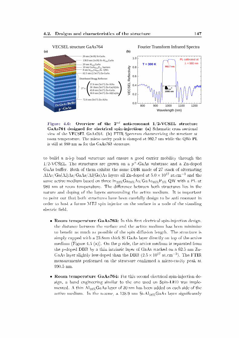
4.2. Designs and characteristics of the structure 147
800 900 1000 1100 12000.0
0.2
0.4
0.6
0.8
1.0
T = 300 K
Bragg
=
1006 nm
PL calibrated at:
= 980 nm
992.7 nm
VE
CS
EL R
eflectivity
Wavelength (nm)
VECSEL structure GaAs764 (a) (b)
(c)
72.6 nm (5e17) Zn-AlAs
Distributed Bragg Reflector:
57.6 nm (5e17) Zn-AlAs
30 .0nm (5e17) Zn-Ga(Al)As
43.8 nm (5e17) Zn-GaAs
30.0 nm (5e17) Zn-Al(Ga)As ( ) 27 x
62.5 nm (2.5e17) Zn-GaAs
20 nm (3e18) Si-GaAs
8 nm In20%Ga80%As QWs 10 nm GaAs95%P5% barriers
20 nm Al18%GaAs
138.9 nm (1e18) Si-Al18%GaAs
Fourier Transform Infrared Spectra
Figure 4.6: Overview of the 2nd anti-resonant 1/2-VCSEL structure
GaAs764 designed for electrical spin-injection: (a) Schematic cross sectional
view of the VECSEL GaAs764. (b) FTIR Spectrum characterizing the structure at
room temperature. The micro-cavity peak is clamped at 992.7 nm while the QWs PL
is still at 980 nm as for the GaAs763 structure.
to build a n-i-p band structure and ensure a good carrier mobility through the1/2-VCSEL. The structures are grown on a p+-GaAs substrate and a Zn-dopedGaAs buer. Both of them exhibit the same DBR made of 27 stack of alternatingAlAs/Ga(Al)As/GaAs/Al(Ga)As layers all Zn-doped at 5.0× 10¹⁷ at.cm−3 and thesame active medium based on three In22%Ga78%As/GaAs95%P5% QW with a PL at980 nm at room temperature. The dierence between both structures lies in thenature and doping of the layers surrounding the active medium. It is importantto point out that both structures have been carefully design to be anti-resonant inorder to host a future MTJ spin-injector on the surface in a node of the standingelectric eld.
• Room temperature GaAs763: In this rst electrical spin-injection design,the distance between the surface and the active medium has been minimizeto benet as much as possible of the spin diusion length. The structure issimply capped with a 23.8nm thick Si-GaAs layer directly on top of the activemedium (Figure 4.5 (a)). On the p-side, the active medium is separated fromthe p-doped DBR by a thin intrinsic layer of GaAs stacked on a 62.5 nm Zn-GaAs layer slightly less doped than the DBR (2.5× 10¹⁷ at.cm−3). The FTIRmeasurements performed on the structure conrmed a micro-cavity peak at990.5 nm.
• Room temperature GaAs764: For this second electrical spin-injection de-sign, a band engineering similar to the one used on Spin-LED was imple-mented. A thin Al18%GaAs layer of 20 nm has been added on each side of theactive medium. In the n-zone, a 138.9 nm Si-Al18%GaAs layer signicantly

148Chapter 4. Spin injection into Vertical External Cavity Surface
Emitting Lasers
increases the distance between the surface and the active medium which couldmodify the percentage of spin-polarized carrier reaching the QW. The FTIRmeasurements performed on the structure conrmed a micro-cavity peak at992.7 nm.

4.3. Vectorial Analysis of spin-injected VECSEL 149
4.3 Vectorial Analysis of spin-injected VECSEL
In this section, we examined the conditions for the control of the electromagneticeld polarization by discussing the competition between the linear birefringence,intrinsic to the 1â2-VCSELs, and the circular gain dichroism originating from thespin-injection.
4.3.1 Inuence of birefringence and dichroism on the polarizationselection
4.3.1.1 Mathematical formalism
We consider a cold cavity exhibiting a residual phase anisotropy that xes the polar-ization states in the cavity. The Jones matrix associated with the phase anisotropyγ can be written as:
[J∆φ] = exp
(−j 2π
λ0nl
)·
(exp(−jγ) 0
0 exp(jγ)
)(4.1)
where λ0 is the average laser wavelength, l the cavity optical length and n =ne+no
2 the average optical index, ne and no being respectively the extraordinary andordinary optical index of the birefringent component. A reduced expression of thephase anisotropy for a single path in the cavity is given by:
γ =π
λ0(ne − no) l (4.2)
In these conditions, the cold cavity admits two eigen states of the electric eldlinearly-polarized along the ordinary and extraordinary axis of the residual phaseanisotropy.
Here, we are trying to study if a gain circular dichroism generated by spin-injection can trigger a modication of the laser eigen states, and in particular en-gender circularly-polarized eigen states as previously observed in the litterature [36,283, 43, 224, 37]. The Jones matrix associated with this gain circular dichoism ∆G
induced by a spin population imbalance is:
[J∆G] =
(G − i
2∆G
i2∆G G
)(4.3)
where G = G++G−2 represents the average gain, G+ and G− being the gains
seen by the right- and left- circular polarizations respectively. This gain circulardichroism can then be expressed as:

150Chapter 4. Spin injection into Vertical External Cavity Surface
Emitting Lasers
Figure 4.7: Schematic representation of the studied cavity: The residual linear
birefringence of the cold cavity induces a phase anisotropy γ. The ordinary (optical
indice no) and extraordinary (optical indice ne) axis are oriented along the x- and
y-axis respectively. The light propagation occurs along the z-axis. The gain circular
dichroism ∆G is induced by optical or electrical spin-injection. We dene l as the
optical length of the laser cavity and λ0 as the central laser wave length. The output
mirror M has a reectivity R while the input mirror is considered perfectly reecting
and non-birefringent.
∆G = G+ −G− (4.4)
One can note that such a matrix does not introduce any phase anisotropy for theright- and left- circular polarization. However, it introduces a phase term when theincident polarization is linear. This phase term introduces an elliptical polarizationcomponent which ellipticity increases with ∆G. In other words, the gain circulardichroism projects the electric eld on the orthogonal state.
We assume that the input mirror is perfectly reecting and does not exhibit anybirefringence. It can consequently be neglect in the vectorial model. Note thatthis hypothesis is not restrictive as it is possible to account for an eventual residualbirefringence of the miror in the previously introduced phase anisotropy term [J∆φ].We write the Jones matrix for the output mirror as:
[JM ] =√R
(1 0
0 1
)(4.5)
We now assume that the residual birefringence axis are oriented along x andy and we consider z has the light propagation axis (Figure 4.7). We can now ex-press the Jones matrix representing the global spin-injected VECSEL at the outputmirror:

4.3. Vectorial Analysis of spin-injected VECSEL 151
[JL] = exp(jφ) · [J∆φ] [J∆G] [J∆φ] [JM ] (4.6)
The Jones matrix [JL] represents the gain for a round-trip in the active medium.The term exp(jφ) accounts for the accumulated phase during the eld propagationin the laser cavity. By developing the expression we nd:
[JL] =√RG · exp (−2jkLeff ) ·
exp(−2jγ) − i2∆GN
i2∆GN exp(2jγ)
(4.7)
where k = 2πνc is the wave number linked to the oscillation frequency and ∆GN =
∆GG
is the normalized value of the gain circular dichroism. Leff = nameam + nl+L
is the average optical length of the laser cavity with nam and eam standing for theoptical index and the thickness of the active medium respectively. L is the cavitylength without the active medium and the birefringent component (L = 0 for amonolithic VCSEL).
The resonance condition of the electric eld ~E for a round-trip in the cavity im-poses that:
[JL] ~E = λ~E (4.8)
where λ are the eigen values. The system admits two eigen states accordinglyto the two degrees of freedom of the problem. The diagonalization of [JL] leads tothe identication of the eigen values and polarization eigen states. The equationassociated with the eigen value is:
(λ− cos 2γ)2 =1
4∆G2
N − sin2 2γ (4.9)
The resolution of this equation gives access to the oscillation frequencies and thesaturated gain:
λ =1√RG· exp (−2jkLeff ) (4.10)
We can now identify from equation (4.9) the dierent oscillation regimes of thelaser.

152Chapter 4. Spin injection into Vertical External Cavity Surface
Emitting Lasers
4.3.1.2 Identication of the oscillation regimes
In this section we study the dierent oscillation regime of the laser arising fromequation (4.9) . Several situation can be identied depending on the relative in-uence of the linear birefringence γ and the gain circular dichroism ∆G. We startby describing two limit cases where either ∆G = 0 or γ = 0. Then, we depict themost general case corresponding to our experimental situation where ∆G 6= 0 andγ 6= 0. The goal here is to theoretically understand the conditions required to makea spin-injected VECSEL oscillate on circularly polarized eigen modes.
A) Limit cases:
1. If there is no gain circular dichroism: ∆G = 0
This particular situation corresponds to the case of a spin-unpolarizedpumping. Indeed a nonexistent ∆G is directly equivalent to an evenpopulation of spin-up and spin-down in the active medium of the laser.in this case, only the residual linear birefringence γ remains. The diag-onalization of [JL] gives two eigen states Ex and Ey linearly-polarizedalong the ordinary (x-) and extraordinary (y-) axis of the linear birefrin-gence. The equation (4.9) becomes:
(λ− cos 2γ)2 = cos2 2γ − 1
λ± = exp(±2jγ)(4.11)
where λ± eigen values verifying the associated equation. As a conse-quence, the frequency dierence between both eigen state is:
∆ν = νy − νx =cγ
πLeff(4.12)
This situation features the usual behavior of a dual-frequency laser ex-hibiting two eigen polarization states linearly polarized along the axis ofthe birefringent crystal. Additionally, the two eigen frequencies are notdegenerated and the frequency detuning is directly proportional to thelinear birefringence of the crystal.
2. If there is no linear birefringence: γ ∼= 0
This particular situation is quite unlikely to naturally happen and soto be experimentally observe as semiconductor lasers always exhibit aresidual component of linear birefringence. Anyway, if this ideal systemis pumped with spin-polarized carrier (∆G 6= 0), the diagonalization of[JL] leads to:

4.3. Vectorial Analysis of spin-injected VECSEL 153
ExEy
= ±i = exp(±iπ
2
)(4.13)
The eigen states are right- and left-circularly polarized. Moreover, asthe cavity does not contain any circular birefringent element, both eigenstates are degenerate in frequency. In this conguration the equation(4.9) becomes:
(λ− 1)2 =
1
4∆G2
N
λ± = 1± 1
2∆GN
(4.14)
Both eigen values are real and as their phases are equal to zero botheigen states are degenerate in frequency: ∆ν = 0. Nevertheless, as thesetwo eigen values do not have the same modules, a gain dierence risesbetween the two eigen states:
G± =1√
R(1± 1
2∆GN) (4.15)
During laser operation, this means that an eigen state is going to startoscillating before the other one while increasing the pumping. When thepumping power becomes suciently high the second eigen state will startoscillating as long as the non-linear coupling constant C remains inferiorto 1 (which is the case for our VECSEL: C ' 0.9). For instance, if∆GN > 0 the right-circularly polarized mode will start oscillating rst.
Assuming the self-saturation coecients βR(L) and cross-saturation coef-cients θRL(LR) are identical for both polarization modes (βR = βL andθRL = θLR), similar intensities for both eigen states should be expectedfar from threshold. Moreover, as the two eigen states are degenerate infrequency, increasing the pumping also induces a polarization transitionregime. Close to threshold, the laser is perfectly circularly polarized asonly the σ+-polarized eigen state (lower threshold) is lasing. Rather, farfrom threshold both σ+- and σ−-circularly-polarized modes are oscillat-ing with the same intensity in the cavity leading to a linearly-polarizedoutput polarization (l = 50% σ+ + 50% σ−). In other word the laserDoCP should drastically decrease as soon as the second eigen states startoscillating. This situation precisely ts the experimental observation re-alized by Iba et al. with an optically pumped (110)-VCSEL [42].

154Chapter 4. Spin injection into Vertical External Cavity Surface
Emitting Lasers
B) General case: ∆G 6= 0 and γ 6= 0
This non-trivial situation closely describes an actual experiment of spin-injectionin a V(E)CSEL. Both the residual linear birefringence and the gain circu-lar dichroism induced by optical or electrical spin-injection are consideredhere. To clarify the problem, we further assume that ∆G > 0 and γ > 0.We remind the expression of the equation associated with the eigen values:(λ− cos 2γ)2 = 1
4∆G2N − sin2 2γ (eq. 4.9). Accordingly, three situation must
be considered.
1. The linear birefringence is dominant: 14∆G2
N < sin2 2γ
In this case, equation (4.9) admits two complex solutions:
λ± = cos 2γ ± i√
sin2 2γ − 1
4∆G2
N (4.16)
The imaginary term straightly causes a frequency degeneracy breakingand each polarization eigen state now has its own eigen frequency. Bydeveloping equation (4.9) one can express the frequency detuning betweenthe polarization eigen states:
∆ν =c
2πLeffarctan
√
sin2 2γ − 14∆G2
N
cos 2γ
(4.17)
Figure 4.8 illustrates the evolution of this frequency detuning as a func-tion of the gain circular dichroism for a xed birefringence value. When∆GN increases the frequency detuning ∆ν decreases with a non-linearbehavior until a phase lock is triggered for 1
4∆G2N = sin2 2γ.
Concerning the evolution of the polarization eigen states, the electric eldcomponent verify the following relation:
EyEx
= −2 sin 2γ
∆GN
1±
√1−
∆G2N
4 sin2 2γ
(4.18)
The system admits two linearly-polarized solution which respective ori-entations depend on the ratio between the gain circular dichroism andthe linear birefringence (gure 4.9 (a)-(b)).
2. The linear birefringence and the gain circular dichroism are of
equal magnitude: 14∆G2
N = sin2 2γ

4.3. Vectorial Analysis of spin-injected VECSEL 155
Δν
(Fra
ctio
n o
f F
SR
)
ΔGN/2sin(2γ)
Figure 4.8: Evolution
of the frequency detun-
ing between the two po-
larization eigen states as
a function of the ratio
between the Gain Circu-
lar Dichroism ∆GN and
the linear birefringence
γ. Here γ is taken as 1.
In dynamics operation of spin-injected V(E)CSEL, this particular opera-tion regime comes out as a punctual transition phase between two polar-ization regimes. Both eigen states are linearly-polarized along the samedirection and degenerate in frequency. There is no way of distinguishingthem and everything happens as if there was only one linearly-polarizedeigen state oriented at -45 from the birefringence axis. Equation (4.9)becomes:
(λ− cos 2γ)2 = 0
λ± = cos 2γ(4.19)
And accordingly to the ∆G > 0 and γ > 0 hypothesis, the electric eldcomponents verify:
EyEx
= −1 (4.20)
Which is well in line with a linear polarization oriented at -45 from thebirefringence axis (along x and y). The boundary condition between theB.1 and B.2 situation is correctly verify.
3. The gain circular dichroism is dominant: 14∆G2
N > sin2 2γ
In this case, equation (4.9) admits two real solution:
λ± = cos 2γ ±√
1
4∆G2
N − sin2 2γ (4.21)
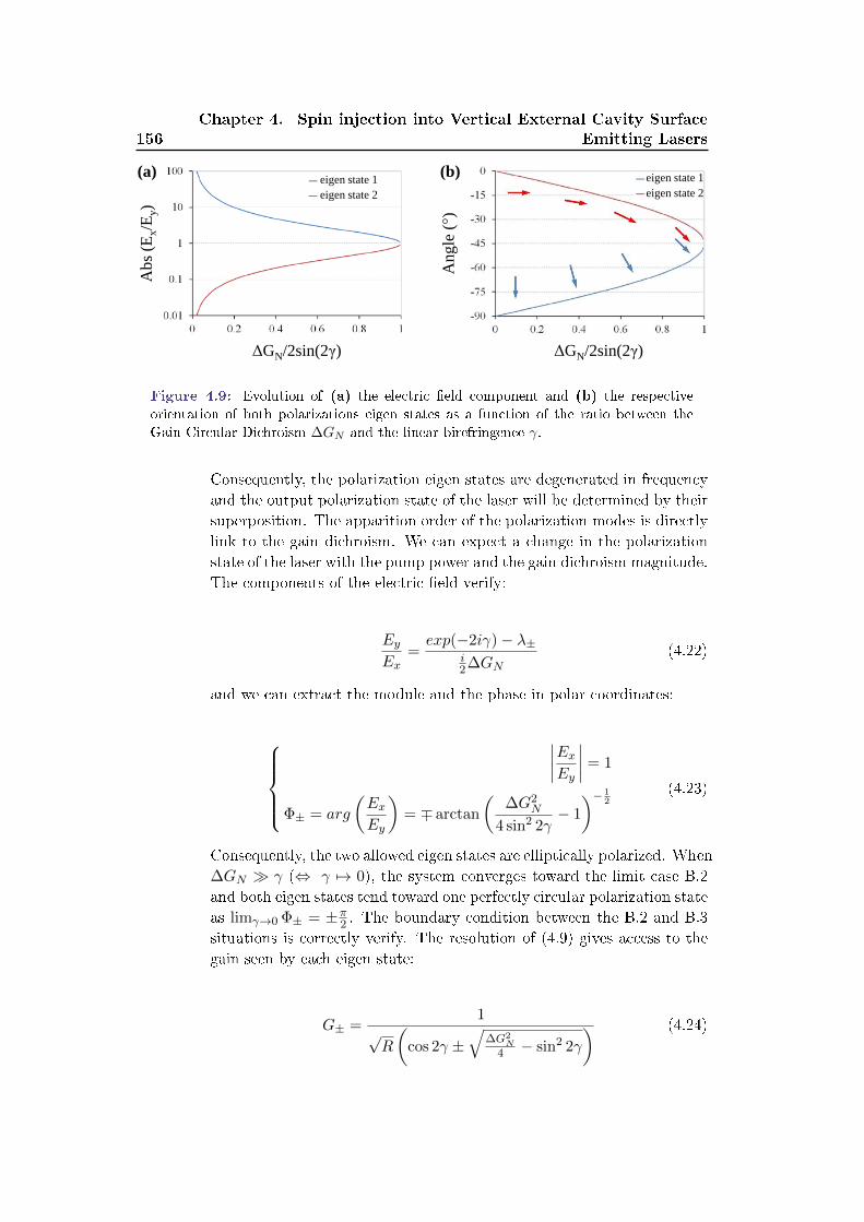
156Chapter 4. Spin injection into Vertical External Cavity Surface
Emitting LasersA
bs
(Ex/E
y)
ΔGN/2sin(2γ)
(a) eigen state 1
eigen state 2
ΔGN/2sin(2γ)
An
gle
(°)
(b) eigen state 1
eigen state 2
Figure 4.9: Evolution of (a) the electric eld component and (b) the respective
orientation of both polarizations eigen states as a function of the ratio between the
Gain Circular Dichroism ∆GN and the linear birefringence γ.
Consequently, the polarization eigen states are degenerated in frequencyand the output polarization state of the laser will be determined by theirsuperposition. The apparition order of the polarization modes is directlylink to the gain dichroism. We can expect a change in the polarizationstate of the laser with the pump power and the gain dichroism magnitude.The components of the electric eld verify:
EyEx
=exp(−2iγ)− λ±
i2∆GN
(4.22)
and we can extract the module and the phase in polar coordinates:
∣∣∣∣ExEy
∣∣∣∣ = 1
Φ± = arg
(ExEy
)= ∓ arctan
(∆G2
N
4 sin2 2γ− 1
)− 12
(4.23)
Consequently, the two allowed eigen states are elliptically polarized. When∆GN γ (⇔ γ 7→ 0), the system converges toward the limit case B.2and both eigen states tend toward one perfectly circular polarization stateas limγ→0 Φ± = ±π
2 . The boundary condition between the B.2 and B.3situations is correctly verify. The resolution of (4.9) gives access to thegain seen by each eigen state:
G± =1
√R
(cos 2γ ±
√∆G2
N4 − sin2 2γ
) (4.24)

4.3. Vectorial Analysis of spin-injected VECSEL 157
Δν
(Fra
ctio
n o
f F
SR
)
ΔGN/2sin(2γ)
eigen state 1
eigen state 2
Figure 4.10: Evolution of the frequency detuning and the polarization state of both
polarizations eigen states as a function of the ratio between the Gain Circular Dichroism
∆GN and the linear birefringence γ.
Experimentally, the eigen state with the highest gain will start lasing rst.As already discussed, if the non-linear coupling between both eigen stateis less than 1 (C < 1), the eigen state with less gain will still oscillate farfrom threshold for a higher pumping rate. The apparition of this secondorthogonally polarized eigen state will generate a diminution of the laserDoCP. Finally if C ≥ 1 only one eigen state will oscillate on the wholepumping range and in this case the DoCP will keep increasing with thepumping power.
4.3.1.3 Synthesis and conclusion
Figure 4.10 summarize the results of the previous section, namely the vectorial be-havior of a spin-injected V(E)CSEL with an active medium exhibiting a gain circulardichroism and cavity presenting a residual linear birefringence. Notwithstanding itsimportance, a linear birefringence is always taking place in a laser mainly due tothe residual strain of the material or in the optical element constituting the lasercavity.
We show that when there is no gain circular dichroism (spin-unpolarized pumping),the laser eigen states are both linearly polarized with a frequency detuning propor-

158Chapter 4. Spin injection into Vertical External Cavity Surface
Emitting Lasers
tional phase anisotropy originating from the birefringent element. These two eigenstates are orthogonal. Then, when the gain circular dichroism increases, the twoeigen states lose their orthogonality and both polarizations tend toward one commondirection while staying linearly polarized. The eigen frequencies remains roughlyconstant. Finally, when the gain circular dichroism becomes sucient enough, bothpolarization becomes degenerate and a phase lock occurs in such way that distin-guishing the eigen state from one another becomes impossible. They become fullydegenerate and combine in one unique linearly polrized state oriented at 45 fromthe linear birefringence axis.
If the gain circular dichroism keeps increasing, the linear polarization mutate to-ward an elliptical polarization with the long axis oriented at 45 from the neutralaxis of the linear birefringence. Then the ellipticity keeps increasing with the gaincircular dichoism until the modes reach a perfectly circular polarization states. It isimportant to notice that, in the elliptical polarization region, the second orthogonaleigen state can appear. Nevertheless the gain associated with this mode is inferior.If the non-linear Lamb coupling constant C allows the oscillation of both modes(C < 1), the laser output DoCP will decrease when the pump power increases.

4.3. Vectorial Analysis of spin-injected VECSEL 159
4.3.2 Preparation of the laser eigen state
We showed in the previous section that the residual linear birefringence in the activemedium locks the laser on two linearly-polarized orthogonal eigen states. The laserwill consequently naturally oscillate on one of these eigen state or eventually bothdepending on value of the Lamb non-linear coupling constant. However if the laseris under spin-polarized pumping, the induced gain circular dichroism will breakthe modes orthogonality. The modes remain linearly polarized as long as the gaincircular dichroism does not fully compensate the linear birefringence. In other words,to increase the chance of observing a switch from a circularly-polarized mode toanother, there is an interest in preparing the laser to naturally oscillate on circularlypolarized eigen modes. To do so, one has to insert in the laser cavity a non-reciprocalmaterial exhibiting Faraday eect as illustrated in gure 4.11. This second sectionfocuses on the modeling of such a system.
4.3.2.1 Intra-cavity Faraday rotator
The Jones matrix associated with a Faraday rotator is dened as:
[JF ] =
(cos θ − sin θ
sin θ cos θ
)(4.25)
where θ is the rotation angle that the Faraday rotator would induce on a linearpolarization. This rotation angle is proportional to the Verdet constant, the Faradayrotator's thickness and to the applied magnetic eld. It is interesting to point outthat the eigen vectors of such a matrice give two right- and left-circularly polarizedeigen polarization states regardless to the value of θ. In practice, this angle is ad-justed to π
4 in optical isolators to provide a total linear polarization rotation of π2
over a round trip.
In our case, to ensure that the circular birefringence introduced by the Faradayrotator fully compensates the residual linear birefringence of the active medium, theFaraday eect should be maximized by choosing a rotator displaying a rotation an-gle θ = π
4 . The Jones matrix associated with a π4 -Faraday rotator naturally derives
from (4.25):
[Jπ/4F
]=
1√2
(1 −1
1 1
)(4.26)
This matrix mixes the linear polarization states originating from the linear bire-fringence of the active medium.

160Chapter 4. Spin injection into Vertical External Cavity Surface
Emitting Lasers
Figure 4.11: Schematic representation of the studied cavity: We considered
the same laser cavity exhibiting a residual linear birefringence γ and a gain circular
dichroism ∆G. A Faraday rotator F inducing a polarization rotation angle θ is added
to the cavity. The circular birefringence generated by the Faraday rotator compen-
sates the linear birefringence of the cold cavity and prepares the laser to oscillate on
circularly-polarized eigen modes.
Taking account of the inserted Faraday rotator, the total Jones matrix representingthe global spin-injected VECSEL at the output mirror for one light round-trip inthe cavity becomes::
[JL] = exp(jφ) · [JF ] [J∆φ] [J∆G] [J∆φ] [JF ] [JM ] (4.27)
where [J∆φ], [J∆G] and [JM ] are still respectively the Jones matrix of (i) theresidual linear birefringence of the active medium given by equation (4.1), (ii) thegain circular dichroism induced by spin-polarized pumping of the active medium(eq. 4.3), and (iii) of the output mirror given by equation (4.4). In further wekeep the same notation of the previous section. We remind that the normalizedgain dichroism ∆GN account for a round-trip in the active medium while the otherphysical parameters account for a single pass of the optical element in the lasercavity. Furthermore the phase term exp(jφ), representing the accumulated phaseduring the electric eld propagation in the laser cavity, has to take into account theoptical pass in the Faraday rotator so as:
φ = 2k(nameam + nl + nF eF + L) = 2kLeff (4.28)
with nF and eF being the average optical index and the thickness of the Faradayrotator respectively.
The resonance condition of the electric eld ~E for a round-trip in the cavity stillveries:

4.3. Vectorial Analysis of spin-injected VECSEL 161
[JL] ~E = λ~E (4.29)
As in the previous section, the analytic calculation of this matrix and its diag-onalization leads to new polarization eigen states of the laser with the associatedeigen values. In the particular case of a Faraday rotator with θ = π
4 the equationssignicantly simplify and the equation associated with the eigen values is given by:
λ± = (∓2−∆GN ) · exp(iπ
2
)= (2±∆GN ) · exp
(∓iπ
2
)(4.30)
As it was predicted, the residual phase anisotropy γ no longer inuences theequation associated with the eigen values and consequently the selection of theeigen polarization states oscillating in the laser.
4.3.2.2 New oscillation regimes
A) Associated eigen values:
The situation is similar to the case A.2) where γ ∼= 0 of the previous section.The only dierence is that here the system is experimentally observable asit is articially prepared to imitate such a situation. The amplitude term ofequation (4.30) gives the gain seen by each eigen state while the argumentprovide access to the eigen frequencies:
G± =
1√R(1± 1
2∆GN)
ν± =
(q ± 1
4
)c
Leff
(4.31)
with q ∈ N. The frequency dierence between both eigen states is given by:
∆ν± = |ν+ − ν−| =c
4Leff(4.32)
This frequency dierence is independent of the residual linear phase anisotropyof the active medium. It is xed by the Faraday rotator and correspond toexactly half of the laser Free Spectral Range (FSR).
B) Associated eigen vectors:
The diagonalization of [JL] leads to the identication of the laser eigen states.The transverse components of the electric eld are expressed as:

162Chapter 4. Spin injection into Vertical External Cavity Surface
Emitting Lasers
Figure 4.12: Evolution
of the transverse compo-
nents of the electric eld
as a function of the linear
birefringence γ in the ac-
tive medium.
Abs
(Ex/E
y)
γ (°)
eigen state 1
eigen state 2
EyEx
∣∣∣∣±
= −i tan(2γ)± i√
tan2(2γ) + 1 (4.33)
This expression highlights how the transverse components of the electric eldremains in quadrature (constant π
2 -dephasing) for each eigen states. Fur-thermore, as the gain circular dichoism does not appear in the equation, theinjected electronic spin will not change the laser eigen polarization but canstill induce a switch from an eigen state to another. However, as shown bythe gain equation (4.31), the gain circular dichroism will favor an eigen stateover the other which will preferentially start lasing rst because of its lowerthreshold.
Figure 4.12 illustrates the evolution of the electric eld's transverse compo-nents for both eigen states as a function of the active medium's linear birefrin-gence. A clear singularity appears for γ = 45, when the circular birefringenceof the Faraday rotator and the linear birefringence of the active medium per-fectly compensate each other. We can distinguish three situations:
1. If there is no linear birefringence: γ 7→ 0
If there is no linear phase anisotropy, the transverse components of theelectric eld are linked by:
EyEx
∣∣∣∣±
= ±i (4.34)
The two eigen polarization are respectively right- and left-circularly po-larized.

4.3. Vectorial Analysis of spin-injected VECSEL 163
(b)
Δν
(Fra
ctio
n o
f F
SR
)
γ (°)
Ab
s (E
x/E
y)
(a)
γ (°)
eigen state 1
eigen state 2
Figure 4.13: (a) Evolution of the electric eld transverse components of both polar-
ization eigen states as a function of the linear birefringence γ. (b) Frequency detuning
between the two polarization eigen states as a function of the linear birefringence γ.
2. If γ = 45:
This scenario is anecdotal and unlikely to happens on real systems as thelinear birefringence remains residual. A Taylor expansion around γ = 45
enables to identify the eigen states:
limγ→π
4
EyEx
∣∣∣∣+
= −∞ limγ→π
4
EyEx
∣∣∣∣−
= 0 (4.35)
In this limit case both polarization becomes linear and oriented along theneutral axis of the linear birefringence (x and y)
3. General case:
In this realistic situation, the eigen states are right- and left-ellipticallypolarized with an ellipticity ranging from perfectly circular (for ∆GN γ ⇔ γ 7→ 0) to linear (for γ = 45) (Figure 4.13). The ellipticityof both polarization states decreases when the linear phase anisotropyincreases. However, experimentally both polarization states should bealmost perfectly circularly-polarized as the linear birefringence remainsresidual compare to the circular birefringence introduced by the Faradayrotator.
4.3.2.3 Synthesis and conclusion
The insertion of a Faraday rotator in the VECSEL's cavity enables to prepare thelaser to oscillate on eigen states conducive to the observation of the inuence ofspin-injection on the laser polarization. We theoretically showed that such an opti-cal device oers the possibility to mask the impact of the residual linear birefringence

164Chapter 4. Spin injection into Vertical External Cavity Surface
Emitting Lasers
of the active medium by conferring to the laser right- and left-circular eigen polariza-tions. If so, the gain circular dichroism produced by spin injection directly generatesa gain disequilibrium between these polarization modes, that can eventually lead toa polarization switch if the non-linear Lamb coupling constant is high enough. Inaddition, this vectorial model shows that the frequency detuning between the twolaser eigen states is equal to half the laser FSR regardless to the linear birefringencevalue.
4.4. Birefringence measurements 165
4.4 Birefringence measurements
4.4.1 Introduction
We saw in the previous section that the residual linear birefringence γ plays a pre-dominant role in the polarization selection of VECSEL. Accordingly, it is necessaryto quantify the birefringence in the structure in order to better understand the rel-ative impact of the birefringence (intrinsic to 1/2-VCSEL) and the gain circulardichroism ∆GN (from the spin-injection) on the polarization selection. The studyof the γ
∆GN-ratio should enable us to estimate the minimum gain circular dichroism
∆GN required to take over the control of the modes' polarization. This study hasbeen recently submitted for publication to the journal Optics Express [261].
V(E)CSEL provide a relatively good isotropic emission as there is no preferentialguiding for TE- or TM- modes like in conventional laser diodes. Nevertheless resid-ual stress [263], lattice strains [251, 344], temperature variations [274, 227], thecavity geometry [265, 244, 345], a high number of strained-balanced QW or evenlithography processing of VCSEL can break this in-plane symmetry and give rise tolinear birefringence in the structure. In the particular case of 1
2 -VCSEL, the lack oftop Distributed Bragg Reector (DBR) is suspected to increase the lattice strains onthe active medium and induce an increase of residual linear birefringence comparedto regular VCSEL. For our (100) QW VECSEL, the typical linear polarization axisare along [011] (TM) and [011] (TE) with a preferential selection for the [011] di-rection.
In this section we report birefringence measurements of a VECSEL structure bymeasuring the frequency detuning between two orthogonal linearly-polarized modes.Previous birefringence estimations based on frequency detuning measurements havebeen reported in the literature but only for monolithic VCSEL and by performinga direct optical detection [250]. Hendriks et al. performed birefringence measure-ments in the optical domain using a noise-eater to improve the stability of the laserpump combined with a planar Fabry-Perot interferometer. The Fabry-Perot exhib-ited a free spectral range FSR ≈ 29.3 GHz, a nesse F ≈ 100 and accordingly amaximal resolution R = 293 MHz
(R = FSR
F
). Using this setup they quantied a
birefringence γ′
2π ≈ 2× 10⁻⁴ rad in a 3 GaAs-QW monolithic VCSEL. The spectralresolution of such Fabry-Perot interferometers is sucient to measure the frequencydetuning between the TE- and TM- modes of few GHz displayed by monolithicVCSEL (micro-metric cavities). However in the case of VECSEL with long cavities(cm) the frequency detuning is expected as low as few MHz. Consequently the spec-tral resolution of such Fabry-Perot interferometers is insucient. To overcome thislimitation we transferred the optical frequency detuning between the two TE- andTM- modes into the electrical domain. Then, we performed the frequency detuningmeasurements using an Electrical Spectrum Analyzer (ESA) near the rst adjacentmode where the noise oor is at the shot noise (Figure 4.14).

166Chapter 4. Spin injection into Vertical External Cavity Surface
Emitting Lasers
M
f1
f2
Pe
ltier
VECSEL
f3 Polarizer YAG 100m
f4
Photodiode
Am
plifie
r
L
Spectrum Analyzer
Longitudinal
y
x λ/2
Vertical
z
y
Two Orientations:
VECSEL
[0-11]
[011]
Inset 1: Optical spectrum
(Raw emission)
Oscillating mode
Optical
Frequency (ν)
o
e
o
e
o
e
order p-1
order p
order p+1
Δν Δν
νep
νop
νep+1
νop+1
νep-1
νop-1
Inset 2: Optical spectrum
(After Polarizer at 45°)
e
Optical
Frequency (ν)
o o e o
e order p-1
order p
order p+1
Δν Δν
FSR
νep
νop
νep+1
νop+1
νep-1
νop-1
Inset 3: RF spectrum
(After Polarizer at 45°)
Electrical
Frequency (f)
f0
0
Region of Interest
f2 f3
f1
Figure 4.14: Outline schematic illustrating the principle of the experiment:
Experimental setup is composed of: L = 23mm, f1 = 10mm, f2 = 25mm, f3 =
175mm, M : (R = 25mm,T = 0.5%). The Insets 1, 2 and 3 illustrate the evolution
of the emitted raw optical spectrum (Inset 1) after projection through a 45-polarizer
(Inset 2) and conversion into a RF spectrum by a photodiode (Inset 3). In the optical
spectrum, the ordinary and extraordinary polarization are represented in red and blue
respectively. In the electrical spectrum, the beating between modes are identied by
the frequencies f0 = νpe − νpo , f1 = νpe − νp−1e , f2 = νpe − νp−1
o and f3 = νp+1o − νpe . The
self-beatings of a mode with itself between dierent order is represented in purple while
the cross-beatings between two dierent modes is represented in orange (regardeless to
the mode orders).
4.4.2 Experimental setup
The experimental setup is described in Figure 4.14. We used an anti-resonant 12 -
VCSEL (GaAs615) grown by Metal Organic Chemical Vapor Deposition (MOCVD)consisting in a 27.5-period GaAs/AlAs Bragg mirror (99.9% reectivity). The gainat λ=1 µm is ensured by twelve strained balanced In22%Ga78%As/GaAs95%P5% QWin a 13λ/2 cavity. The sample consists in a 10×5 mm2 clived and non-processedpiece of raw wafer. The structure is maintained at 282 K with a Peltier thermo-electric cooler throughout the whole experiment. Instead of clamps, the VECSEL

4.4. Birefringence measurements 167
is mounted on the Peltier with thermal grease to avoid any parasitic stress on thestructure that could bias the measurements. The pumping system consisted in a808 nm pigtail multimode laser diode delivering up to 2 W and focused on the gainmedium to a 100µm spot with a 30 incidence angle. The VECSEL is pumped inthe continuous regime throughout the experiment. The linear cavity is closed by a25 mm radius of curvature concave mirrors M with a 0.5% transmission at 1 µm(Figure 4.14). The cavity length was set to 2.3 cm and exhibits a net round-triplosses of 1% giving a photon lifetime of 7.4 ns, which is higher than the carrier life-time in stimulated emission regime at about twice the threshold (around 1 ns). Sucha long cavity implies that the laser is highly multimode longitudinally. We then in-troduced and carefully adjusted a 100 µm thick Yttrium Aluminum Garnet (YAG)crystal inside the laser cavity to set the laser monomode and focused on the obser-vation of the rst adjacent mode to avoid any spectral aliasing. The VECSEL isthen oscillating on one linearly-polarized mode and the amplied spontaneous emis-sion of the orthogonal polarization mode is still detectable above the shot-noise. Atthe output of M the beam is collimated (f3) and we realize a ber-coupling with amonomode optical ber to send the emitted light on a photo-diode. The electricalsignal obtained is then amplied using a low noise, high bandwidth amplier andsent to an ESA. Between the output coupler and the ber-coupling, we inserted apolarizer to project the orthogonal linear polarizations of the lasing mode and theamplied spontaneous emission on the same optical axis (Figure 4.14 Inset 2). Inthe electrical domain, we focus on the beatings between these two linearly-polarizedmodes near the rst adjacent mode. On the ESA, the central peak (f1) correspondsto the self-beating of the lasing mode between adjacent orders while the two smallersatellite peaks (f2 and f3) on each side correspond to the cross-beating between thetwo modes (Figure 4.14 Inset 3).
The birefringence γ′ is extracted from the frequency detuning measurements ∆f .∆f represents the frequency shift between the central peak f1 and the satellite peaksf2 and f3. By considering that the TE-mode is the mode lasing in the cavity, thecentral peak f1 corresponding to the self-beating of the TE-mode while the twosatellite peaks f2 and f3 on each side correspond to the beating between the TM-and TE-modes (Figure 4.14 Inset 3). In the optical domain, the frequencies νpTEand νqTM associated with the TE- and TM-polarization modes at the optical orderp and q are respectively given by:
νpTE = p · c
2 [L+ (ne − 1)l]
νqTM = q · c
2 [L+ (no − 1)l]
(4.36)
where L is the cavity length, c is the celerity of light and l is the thickness ofthe active medium. ne and no are the optical index seen in the VECSEL alongthe extraordinary and ordinary polarizations respectively. As the birefringence is

168Chapter 4. Spin injection into Vertical External Cavity Surface
Emitting Lasers
Figure 4.15: Ampli-
tude variations of the
projected orthogonal po-
larization modes as a
function of the polarizer
angle θ for the VEC-
SEL oriented longitudi-
nally at T=282 K and
for a pumping power
Ppump = 515 mW. The
inset presents the vari-
ations of the amplitude
maximum as a function
of the polarizer angle for
the frequencies f1 and
f2.
expected to be relatively small, we assume the relation p=q for the optical orders.After projection of the optical spectrum through a 45-polarizer, we can show thatin the electrical domain the birefringence is linked to the frequency detuning by therelation:
γ′
2π=
2L
c·∆f (4.37)
where L ≈ Le = L+(ne−1)l ≈ Lo = L+(no−1)l and c is the light celerity. Thisrelation is established for a round-trip in the cavity. This experimentally measuredbirefringence γ′ and the reduced expression of the linear birefringence γ given for around-trip in the cavity in the vectorial model (Section 4.3.1.1, Eq. 4.2) are linkedby the relation γ′ = 4γ. The formal demonstration of the equation (4.37) can be ndin the Appendix D. The birefringence measured for the two orthogonal VECSELorientations [011] and [011] is a combination of the birefringence intrinsic to theVECSEL structure and the birefringence induced by the optical pumping mainlythrough thermal eect.
The VECSEL is class-A as the photon lifetime in the cavity is higher than thecarrier lifetime [333]. In a class-A laser the relaxation oscillations becomes negligi-ble by adiabatic elimination of the population inversion from the laser dynamics.The laser behavior is then exclusively governed by the ltering function of the coldcavity. Thus, one can expect a signicant noise reduction compared to monolithicVCSEL [333]. As opposition with previous measurements reported on class-B VC-SEL [250], the class-A behavior oer by VECSEL ensure a laser noise limited to theshot-noise limit.

4.4. Birefringence measurements 169
In terms of geometrical convention, we consider that the light emitted by the VEC-SEL propagates along the x-axis while the linear polarizations associated with theemission evolve in the (y,z)-plane. The long and the short sides of the VECSELcorrespond to the [011]- and [011]-crystallographic directions respectively. Accord-ingly, we dene the VECSEL "Longitudinally-oriented" when the long side of theVECSEL ([011]-axis) is parallel the the y-axis and "Vertically-oriented" when theshort side of the VECSEL ([011]-axis) is parallel the the y-axis (See Top-Left ofFigure 4.14). Finally, we take for notation conventions to identify the frequency inthe optical domain as ν and the frequency in the electrical domain as f .
4.4.3 Identication of the two linearly-polarized orthogonal modes
In this preliminary experiment, we demonstrate that the Amplied SpontaneousEmission (ASE) of the TM-mode can be used as a local oscillator to generate beatingfrequencies in the electrical domain. The study is performed for dierent polarizerangles θ ranging from 0 to 90. Figure 4.15 displays the RF power evolution ofthe beating frequencies. As already emphasized, the measurements are performednear the rst adjacent mode where the noise oor is minimum (Figure 4.14, Inset3). The amplitude for the central beating frequency (f1) is maximum when thepolarizer is aligned with the polarization direction of the lasing mode (reference:0) and then progressively decreases until complete extinction at 90. Howeverfor the satellite peaks amplitude, the amount of intensity projected increases from0 to 45, where the beating amplitude between the TE- and TM- modes reachesa maximum. Then, by further rotating the polarizer, the measured amplitude ofthe satellite peaks starts decreasing as the projection of the central mode start tovanish, until complete extinction is reached at 90. From 0 to 45, we can clearlysee the opposite amplitude evolution of the central peak f1 and the satellite peaksf2 and f3 (Inset Figure 4.15). This behavior conrms that we are indeed detectinga beating between two orthogonal polarization modes. We also conclude from thispreliminary experiment that the signal to noise ratio for the central and satellitepeaks is maximized by setting the polarizer at 45 from both the TE and TM modes.It is also worthwile to notice that the high nesse external cavity conguration leadsto narrow ASE peaks and thus a high discrimination capability of the experiment.
4.4.4 Birefringence measurements
We performed the frequency detuning measurements for two 1/2-VCSEL orienta-tions. We already know that the structure exhibits a dominant polarization mode(TE) along the [011]-direction with an average gain 10% higher than the orthogonalmode (TM) polarized along the [011]-direction. The pump is by default ellipti-cally polarized with the long axis along the y-axis. We rst place the 1/2-VCSEL's[011]-direction along the y-axis (1/2-VCSEL oriented Vertically) to strengthen thestabilization of the dominant mode. We start by investigating this stabler situation

170Chapter 4. Spin injection into Vertical External Cavity Surface
Emitting Lasers
6.62 6.64 6.66 6.68 6.70 6.72-70
-65
-60
-55
-50
-45
f3
f1
f2
fA
mplit
ude (
dB
m)
Frequency (GHz)
r = 1.03
r = 1.85
Figure 4.16: Frequency spectra of the monomode emission near the rst
adjacent mode for the VECSEL oriented vertically for both low (Black)
and moderate (Green) pumping power: The central peak f1 correspond to the
self-beating of the lasing TE-mode while the two side peaks f2 and f3 both originate
from the cross-beating of the TE- and the TM-mode. For this VECSEL's orientation
∆f ∈ [38.08−40.81] MHz corresponding to a birefringence γ′
2π ∈ [6.3×10⁻³−6.4×10⁻³]
rad. All the measurements were performed at T= 282 K.
before rotating the 1/2-VCSEL in the longitudinal orientation. For both measure-ments we maximize the signal to noise ratio by setting the polarizer at 45 fromthe TE- and TM-mode directions. We dene the pumping rate as being the ratiobetween the applied pumping power (P ) and the threshold power (Pth): r = P
Pth.
VECSEL oriented vertically:
When the 1/2-VCSEL is oriented vertically, the dominant TE-polarization modestarts lasing at threshold (Pth = 295 mW) and prevents the orthogonal TM-modeto oscillate in the cavity due to the gain saturation. Nevertheless, ASE is detectablefor the TM-mode. Accordingly, on the electrical spectrum analyzer we detect theintense central peak associated with the beating of the oscillating mode (TE) withthe ASE in the rst adjacent TE longitudinal mode. Whereas the two satellite peakscorrespond to the beating with the TM-modes. When increasing the pumping ratefrom r = 1.03 to r = 1.85, the amplitude of the three peaks increases (Figure4.16). We also notice a negligible increase of the frequency detuning ∆f betweenthe central and the two satellite peaks due to an increase of the total birefringencein the structure originating from thermal pumping eect. For this range of pump-
4.4. Birefringence measurements 171
ing rate, we measured a frequency detuning ∆f included between 38.08 and 40.81MHz giving an average birefringence value estimated around γ
2π = 6.4 × 10⁻³ rad.However closer to threshold, where the thermal birefringence induced by the pumpis minimum, γ
2π is closer to 6.3× 10⁻³ rad.
At low pumping rate (r=1.03), the slight splitting of the central peak into two peaksis a signature of residual Coherent Population Oscillation (CPO) eect. This eectinduces a non-perfect overlap of the lasing TE-mode with ASE in the longitudinalmodes of order p-1 and p+1. As can be noticed, this behavior which is actually dueto aliasing eects is not present on the satellite peaks because unlike for TE-TE theTE-TM beating of p-1 and p+1 orders with the lasing mode leads to two dierentfrequencies. Moreover, the CPO splitting eect is not expected to play a role forcross-polarized modes because they do not interfere in the active medium. Conse-quently, the accuracy of the birefringence measurement is maximized by consideringthe frequency dierence between the two satellite peaks, that is, 2∆f .
VECSEL oriented longitudinally:
When the 1/2-VCSEL is oriented longitudinally, the TM-mode polarized along the[011] direction starts lasing at threshold (Pth = 316 mW) and the amplied spon-taneous of the [011] orthogonal TE-mode is also observable. On the RF-spectrumwe detect the intense central peak this time associated with the beating of the TMoscillating mode and the TM ASE and the two satellite peaks corresponding tothe beating between the TM oscillating mode and TE ASE. When increasing thepumping rate from r = 1.17 to r = 1.97, the amplitude of the three peaks increases(Figure 4.17 (a)). Here, as opposed to the Vertically-oriented case, we also witness aclear increase of the frequency detuning ∆f between the central and the two satellitepeaks when the pumping power increases: ∆fr=1.17 < ∆fr=1.97. This observationis attributed to an additional birefringence generated by the pump induced thermalstrain increasing the total birefringence in the structure. For this range of pumpingrate, we measured a frequency detuning ∆f included between 33.3 and 40.2 MHzgiving an average birefringence value estimated around γ
2π = 6.12× 10⁻³ rad. How-ever closer to threshold, where the thermal birefringence induced by the pump isminimum, γ
2π is closer to 5.8× 10⁻³ rad.
For pumping rates higher than r = 2.03, a polarization switch is triggered by thethermal birefringence induced by the optical pumping which favors the stability ofthe TE-mode in the cavity (Figure 4.17 (b)). This observation is coherent with pre-vious polarization stability experiment performed on monolithic VCSELs [227, 263].Indeed in our laser system, a polarization bistability regime between the TE- andTM- modes is unlikely to establish due to a non-linear coupling constant C close tounity (C ≈ 0.9) [343, 225]. By further increasing the pumping power, the detectedamplitudes increase until the signal becomes unstable due to the beginning of modehopping and multimode lasing.

172Chapter 4. Spin injection into Vertical External Cavity Surface
Emitting Lasers
6.62 6.64 6.66 6.68 6.70 6.72-70
-65
-60
-55
-50
-45
-40
Am
plit
ud
e (
dB
m)
Frequency (GHz)
r = 1.17
r = 1.97fr=1.97
f1
f3f
2fr=1.17
(a) 6.62 6.64 6.66 6.68 6.70 6.72
-70
-65
-60
-55
-50
-45
-40Polarization
Switch
r = 1.97
r = 2.03
TE
Am
plit
ud
e (
dB
m)
Frequency (GHz)
TM
f1
f3f
2
(b)
Figure 4.17: Frequency spectra of the monomode emission near the rst
adjacent mode for the VECSEL oriented longitudinally: (a) Frequency de-
tuning measurement for both low (Black) and moderate (Green) pumping power. For
this VECSEL's orientation ∆f ∈ [33.3 − 40.2] MHz corresponding to a birefringenceγ′
2π ∈ [5.8 × 10⁻³ − 6.12 × 10⁻³] rad. (b) For pumping rates r = 2.03, a polariza-
tion switch is triggered by a pump induced birefringence favoring the stability of the
TE-mode in the cavity. All the measurements were performed at T=282 K.
4.4.5 Discussion
Comparison analysis:
Figure 4.18 summarizes the birefringence measurements for both the vertical andthe longitudinal orientation of the 1/2-VCSEL. It is important to highlight that thetotal birefringence measured for the two orthogonal VECSEL's orientations [011]
and [011] is a combination of: (i) the intrinsic birefringence of the 1/2-VCSELstructure and (ii) the birefringence induced by the optical pumping mainly throughthermal eects. The average values of birefringence extracted above threshold areγ2π = 6.12 × 10⁻³ rad and γ
2π = 6.4 × 10⁻³ rad for the 1/2-VCSEL oriented lon-gitudinally and vertically respectively. The small dierence witnessed between thetwo orientations can be attributed to the inuence of the pump birefringence. Thepump polarization is elliptical with the long axis oriented along the y-axis. Whenthe 1/2-VCSEL is oriented vertically (dominant polarization (TM) along y-axis) thethermal birefringence induced by the pump slightly enhances the intrinsic birefrin-gence of the semiconductor structure. Oppositely, when the VECSEL is orientedlongitudinally (dominant polarization (TM) perpendicular to y-axis) this thermalbirefringence slightly compensates the intrinsic birefringence of the semiconductorstructure. Accordingly, we estimate the average birefringence of the VECSEL oper-ating in a laser regime to γ
2π ≈ 6.26× 10⁻³ rad.
A more accurate value of the intrinsic birefringence is given for low pumping ratewhere the contribution of the thermally induced birefringence is minimum. Closeto threshold, the average values of birefringence extracted are γ
2π = 5.8× 10⁻³ rad

4.4. Birefringence measurements 173
0 . 8 1 . 0 1 . 2 1 . 4 1 . 6 1 . 8 2 . 0 2 . 2 2 . 45 . 4 x 1 0 - 3
5 . 6 x 1 0 - 3
5 . 8 x 1 0 - 3
6 . 0 x 1 0 - 3
6 . 2 x 1 0 - 3
6 . 4 x 1 0 - 3
6 . 6 x 1 0 - 3
Thres
hold 1 / 2 - V C S E L V e r t i c a l
1 / 2 - V C S E L L o n g i t u d i n a l
γ / 2
π (rad
)
P u m p i n g r a t eFigure 4.18: Birefringence variations as a function of the pumping rate r = P
Pthfor
the VECSEL oriented longitudinally (blue) and vertically (black) at T= 282K.
and γ2π = 6.3 × 10⁻³ rad for the 1/2-VCSEL oriented longitudinally and vertically
respectively. Accordingly, we estimate the average intrinsic birefringence of the1/2-VCSEL to γint
2π ≈ 6.05× 10⁻³ rad.
As anticipated, the birefringence of the 12 -VCSEL is more than 30 times higher
than the birefringence measured by Hendriks et al. in a monolithic 3 GaAs QWsVCSEL γV CSEL
2π ≈ 2×10⁻⁴ rad [250]. Such high values of residual birefringence com-pared to regular VCSEL structures are suspected to emerge from the lack of topdistributed bragg reector inducing a symmetry breaking of the crystalline structureclose to the active medium (≈ 100-200 nm). This symmetry breaking could increasethe lattice strain on the active medium and therefore increase the phase anisotropybetween the ordinary (no) and extraordinary (ne) axis leading to an increase of thelinear birefringence. Additionally, our active medium is build on twelve strained-balanced QWs (to compare with 3-6 for standard VCSEL [42]). The stacking theseInGaAs QWs, each doped with 22% Indium, requires to work with GaAsP barri-ers doped with 5% Phosphorous to generate a compression factor of 0.18 over 560nm and balance the strains in the structure. These strain-balanced QWs are alsosuspected to increase the phase anisotropy in the active medium.
Estimation of the required eective spin-injection:
Thanks to this experimental measurement of γ′, we can now estimate the normalizedgain circular dichroism ∆GN required to compensate the residual linear birefrin-gence of the VECSEL structure. In the previously introduced vectorial model (Sec-tion 4.3) this equilibrium directly translates to: 1
4∆G2N = sin2 γ′
2 . Using the value
174Chapter 4. Spin injection into Vertical External Cavity Surface
Emitting Lasers
γ′exp2π ≈ 6.3× 10⁻³ rad, we calculate that a ∆GN ≈ 4% is necessary to compensate
the linear birefringence. In other words, as ∆GN = 2G+−G−G++G−
this directly meansthat one of the circularly-polarized mode needs to exhibit at least 1.04 times moregain than the other circularly-polarized mode: G+ = 1.04×G− or G− = 1.04×G+.However, one has to keep in mind that this ∆GN value is just an inferior limit atwhich the VECSEL is in an articial isotropic state for the TE- and TM-modes.According to the vectorial model, in this metastable state the TE- and TM-modesare still both linearly polarized and oriented at 45 from the ordinary [011] andextraordinary [011] axis. To trigger VESCEL oscillations on two elliptically- andfurther circularly-polarized modes, one would have to increase ∆GN by boostingthe gain dierential between the two circularly-polarized modes (∆G = G+ −G−).This mode of operation will be reached by improving the eective spin-injection inthe active medium.
Using the same calculation for a regular VCSEL exhibiting a linear birefringenceγ′V CSEL
2π ≈ 2 × 10⁻⁴ rad [250] we nd that a normalized gain circular dichroism8 times inferior ∆GN ≈ 0.5% is sucient to compensate the birefringence in thestructure. This can partly explain the impressive values of DoCP already obtainedwith monolithic VCSEL under optical [36, 41, 283, 42, 43] and electrical [37] spin-injection.
In the next section we are going to experimentally investigate the same GaAs615VECSEL structure under optical spin-injection. The competition between the resid-ual linear birefringence and the gain circular dichroism is studied by analyzing thelight polarization emitted by the VECSEL. Thanks to an original experimentalsetup, we introduce and highlight the fundamental role of the Lamb non-linear cou-pling constant C on the polarization selection.

4.5. Optically spin-injected VECSELs 175
4.5 Optically spin-injected VECSELs
This section presents the experiments and the associated results on optical spin-injection in VECSEL realized during this Ph.D. This work represents a signicantportion of the total experimental work developed during the thesis. The study hasbeen successfully published in Applied Physics Letters [225].
4.5.1 Linear-Cavity VECSEL
To perform the very rst optical spin-injection experiments in VECSEL, we optedfor a simple linear cavity in order to minimize the system complexity. The goal hereis to see if the output polarization of the VECSEL can be monitored by injectionof spin-polarized carriers in the laser active medium through circularly-polarizedoptical pumping.
4.5.1.1 Experimental Setup
For the experiment (gure 4.19) we used an antiresonant n.i.d VECSEL (GaAs615)grown by Metal Organic Chemical Vapor Deposition (MOCVD) consisting in a 27.5-period GaAs/AlAs Bragg mirror (99.9% reectivity). The gain at λ=1 µm is ensuredby twelve strained balanced In22%Ga78%As/GaAs95%P5% QW in a 13λ/2 cavity.The structure is mounted on a Peltier thermo-electric cooler with thermal greaseand maintained at 285 K throughout the whole experiment. The pumping systemconsists in a 808 nm pigtail multimode laser diode delivering up to 2 W and focusedon the gain medium to a 100 µm spot with a 30 incidence angle. The VECSEL ispumped in the continuous regime throughout the experiment and the laser thresholdis measured as being Pthreshold = 200 mW. The pump light is circularly-polarizedafter collimation (f1) using a high power polarizer-cube combined with a λ
4 -wave
M
Pe
ltier
VECSEL
Analizer L
y
x
λ/4
+ 45°
- 45°
σ- σ+
f2
f1
Polarizer
RG1000
Power
meter
34.54 mW
Figure 4.19: Linear-Cavity VECSEL with the associated characterization
setup: f1 = 10mm, f2 = 50mm, M : (R = 50mm,T = 0.5%), L = 50mm.

176Chapter 4. Spin injection into Vertical External Cavity Surface
Emitting Lasers
Circular polarizations: εllipticity ≈ 97%
0
100
200
300
400
500
600
700
020
40
60
80
100
120
140
160180
200
220
240
260
280
300
320
340
0
100
200
300
400
500
600
700
Pump polarization:
+- Polarized
-- Polarized
Op
tica
l P
ow
er
(mW
)
(a)
0
20
40
60
80
100
120
140
160
020
40
60
80
100
120
140
160180
200
220
240
260
280
300
320
340
0
20
40
60
80
100
120
140
160
Optica
l P
ow
er
(mW
)
VECSEL Polarization(b)
Linear polarization: εllipticity = 0%
Figure 4.20: Optical power measurements as a function of an analyzer an-
gle: (a) Pump ellipticity for right- and left-circularly polarized pumping. In both
cases, the combination of a polarizer and a λ4 on the pump setup gives a pump beam
almost perfectly circularly-polarized: ε ≈ 97%. (b) Despite 97% σ+- or σ+-polarized
pumping, the output polarization of the VECSEL remains strictly linear ε ≈ 0%.
plate and then focused on the VECSEL surface (f2). The linear cavity is closed bya 50 mm radius of curvature concave mirrors M with a 0.5% transmission at 1 µm.At the output ofM the polarization orientation of the emitted laser light is analyzedusing a conventional polarizer. A spectral lter RG1000 cutting frequencies below1000 nm is introduced in-between the output coupler and the analyzer to clearlyseparate the laser emission (1000 nm) from any pump reexion (808 nm).
4.5.1.2 Experimental observations
Despite a 100% right (σ +) or left (σ −) circularly-polarized pumping (gure 4.20 (a))the laser output polarization remains strictly linear (gure 4.20 (b)). This can beexplained mainly by the presence of the strong residual linear birefringence γ in thestructure conferring to the laser two linearly-polarized orthogonal eigen states. Ashighlighted in the previous section, such high value of residual linear birefringencecompared to regular VCSEL can emerge from the lack of top DBR and the importantnumber of strained-balanced QW thereby increasing the lattice strain on the activemedium. For our (100) QW VECSEL, the typical linear polarization axes are along[011] (TM) and [011] (TE). To overcome this problem, it is necessary to inserta non-reciprocal material inside the optical cavity in order to generate an intra-cavity circular birefringence suciently high to completely overcome the residuallinear birefringence of the 1/2-VCSEL structure. Additionally, pumping with a 30
incidence angle induces a projection of the circularly-polarized pumping light intoan elliptically-polarized incident light in the plane of the QW. Consequently, theeective transferable angular momentum from the photons to the QW's carriersrequired to eciently generate spin-polarized carriers is signicantly reduced and sois the global spin-injection eciency.

4.5. Optically spin-injected VECSELs 177
λ/4 Polarizer Powermeter
Computer
Control
Unit
σ+ σ-
Pu
mp
f1 f2
D3
Pe
ltie
r
VECSEL
Fabry-Pérot
Interferometer
f3
Polarizer
Faraday
Isolator
M1
M2
M3
M4
D1
D2
D4
Faraday
Rotator
+ 45°
- 45°
λ/4
σ-
σ+ Oscilloscope
Polarimeter’s Head
Figure 4.21: New extended M-cavity VECSEL with the associated char-
acterization setup: f1 = 10mm, f2 = 25mm, M1 : (Plane, T = 0.5%), M2 :
(R = 50mm,T = 0.1%), M3 : (R = 50mm,T = 0.1%), M1 : (Plane, T = 0.1%),
D1 = 224mm, D2 = 55mm, D3 = 54mm, D4 = 226mm.
4.5.2 Extended M-Cavity VECSEL
4.5.2.1 Experimental Setup
To articially introduce a circular birefringence in the cavity and compensate thestrong linear birefringence of the structure, we chose to use a 45 Faraday rotatorconsisting in a Terbium Gallium Garnet (TGG) bar anti-reection coated at 1µmand placed at the center of a cylindrical magnet. Ideally, the optical componentshould induce a circular birefringence so important that the linear birefringenceγ becomes negligible, making this laser inherently oscillate with respect to a leftand/or right circularly polarized light [346]. However, the insertion of such a largeoptical component (10 cm long) in the laser cavity required to re-think the wholeexperiment. The new design of the cavity geometry was driven by two main objec-tives: (i) the rst one was to maximize the spin-injection eciency by pumping theVECSEL with a normal incidence to prevent any elliptical projection of the circularpolarization and (ii) the second point was to prepare the laser to oscillate on twocircularly-polarized eigen states by successfully inserting this large intra-cavity Fara-day rotator. After reexions and optical simulations using the software LaserCalc,a cavity with an extended M-shaped geometry was chosen for stability, exibility,adaptability and compactness reasons.
For this new experiment we used the same 12 In22%Ga78%As/GaAs95%P5%-QWVECSEL (GaAs615) maintained at 285 K with a Peltier thermo-electric cooler. Fig-ure 4.21 schematized the complete experimental setup. The structure is pumped ina continuous regime throughout the experiment and the laser threshold is measuredas being Pthreshold = 300 mW. The pump system consists in the same 808 nm pigtailmultimode laser diode delivering up to 2 W and focused on the gain medium to a100 µm spot with a normal incidence. As previously, the pump light is circularly-polarized after collimation (f1) using a high power polarizer-cube combined with a

178Chapter 4. Spin injection into Vertical External Cavity Surface
Emitting Lasers
0 5 1 0 1 5 2 0 2 5 3 0- 1 0 0- 8 0- 6 0- 4 0- 2 0
02 04 06 08 0
1 0 0
3 . 4 3 . 6 3 . 8 0246
s -s -
s +s + : - 5 . 3 %s - : - 1 . 8 %
s +
Polar
izatio
n Ellip
ticity
(%)
T i m e ( s )
s -
∆t
P P D ( k W / c m 2 )
OOP (
mW)
Figure 4.22: Time evolution of the laser output polarization ellipticity when
switching the pump polarization from σ + to σ −. The inset presents the evolu-
tion at threshold of the Output Optical Power (OOP) as a function of the Pump Power
Density (PPD) for dierent pumping polarization orientations: l linear in black, σ +
in blue and σ − in red. The transition time ∆t correspond to the time needed to rotate
the QWP of the pumping system.
λ4 -wave plate and then focused on the VECSEL surface (f2). The optical cavity iscomposed of ve mirrors including the 1/2-VCSEL DBR, two 99.9% reectivity 50mm radius of curvature concave mirrors (M2, M3) and two plane mirror (M1, M4)to close the cavity. We used 99.5% reectivity forM1 to facilitate the ber-couplingwith a Fabry-Perot interferometer and 99.9% reectivity for M4 to limit the satu-ration of the polarimeter's head. The angle between M2 and M3 was minimized inregard to the limit of the setup and is about 30 . The distances between the mirrorshave been precisely estimated using computer simulations for optimal laser stability.
Finally, the cavity length is 56 cm giving a photon lifetime of 180 ns, which ismuch higher than the carrier lifetime in stimulated emission regime at about twicethe threshold [333] (around 1 ns) ensuring a class-A dynamical behavior for thelaser. Such a long cavity also implies that the laser is highly multimode longitudi-nally. At the output of M1 we used a Fabry-Perot interferometer to visualize thelaser oscillation. The Faraday isolator is used to reduce the laser perturbation bypreventing any photon re-injection in the cavity. The laser polarization is analysedat the output of M4 with a Thorlabs PAX5710 polarimeter combining a rotating1/4-Wave plate (QWP), a polarizer and a Powermeter. Here, the separation of thelaser emission (1000 nm) from pump reexions (808 nm) is done by choosing theright wavelength calibration (980 nm) in the polarimeter software setups.

4.5. Optically spin-injected VECSELs 179
X Scale: 10 ms/Div Y Scale: 20 ms/Div
PD 1
PD 2
Close to threshold: Ppump = 0,9 W
X Scale: 10 ms/Div Y Scale: 20 ms/Div X Scale: 10 ms/Div Y Scale: 50 ms/Div
Ppump = 1,1 W Far from threshold: Ppump = 1,5 W
Coupling increases Switching frequency increases
Figure 4.23: Evolution of the two circularly polarized orthogonal modes when in-
creasing the pumping power.
4.5.2.2 Experimental observations
This time, when manually switching the pump polarization from right to left cir-cular polarization, we observed a corresponding switch from σ + to σ − of the laserpolarization. This witnesses a sucient spin injection in the active medium ofthe 1/2-VCSEL (Figure 4.22). Nevertheless, on the other hand, we observed athreshold reduction of few percent when pumping circularly compare to the linearlypolarized pumping (Inset Figure 4.22). But, the analytical model and the simu-lations presented in section 2.2.3.2 clearly highlight that the threshold reductionunder spin-injection normalized to the threshold under unpolarized injection JT is adirect probe of the spin-injection eciency in the system. Consequently, this weakthreshold reduction characterizes a weak eective spin-population dierence in theactive medium of the laser resulting in a gain dichroism of few percent. The thresh-old reduction dierence between σ + and σ − pumping can be explain by the brokensymmetry between the non-saturated gain of the right- (GR) and left- (GL) circu-larly polarized modes due to geometrical consideration. The laser tends to moreeasily lase on the σ + mode as GR is intrinsically higher than GL.
We also studied the relative dynamic of both circularly polarized modes as a functionof the pump power using a polarization dependent beam splitter, two Photo-Diodes(PD 1 and PD 2) and an oscilloscope. When increasing the pump power, we clearlyidentied an increase of the coupling between both circularly polarized modes behav-ior. The oscillation of one circularly polarized mode in the cavity seems to disablethe oscillation of the orthogonal mode. Additionally, the switching frequency froma mode to another also increases with the pumping power (Figure 4.23).
4.5.3 Analysis of the physical mechanisms: The Lamb model
The mechanisms inducing this complete polarization switch despite such a smalleective spin-injection remain to be understand. We previously showed using a

180Chapter 4. Spin injection into Vertical External Cavity Surface
Emitting Lasers
vectorial model (section 4.3.2) that it is possible to prepare the laser's eigen statesby inserting a Faraday rotator inside the laser cavity. Doing so, the action of a gaincircular dichroism induced by the spin-injection translates into intensity variationsof the eigen states or even a complete switch from an eigen state to another. Sucha conguration is interesting to probe the impact of the spin injection. Indeed,we show that the insertion of the Faraday rotator mask the eect of the residuallinear birefringence in the active medium. Consequently, the gain circular dichroisminduced by the spin-injection directly translates into a gain disequilibrium betweenboth eigen state. This disequilibrium, even weak, can trigger a complete switchfrom an eigen state to the other provided that the non-linear coupling constant ishigh enough (which is the case in our VECSEL). In other words, it is possible tofabricate a laser source exhibiting a high DoCP and for which the switch from aσ+-polarized to a σ−-polarized eigen state can be achieve even with a moderateeective spin-injection.
4.5.3.1 Mathematical formalism
To pull the blind on these mechanisms, we turned toward Lamb Model for a class-A,Two-mode operation laser [268]. The laser being class-A, it is possible to adiabat-ically neglect the population inversion. In this case, the temporal evolution of thetwo modes intensities can be simply described by two coupled dierential equationsof the rst order [268]:
IR = IR (GR − βRIR − θRLIL)
IL = IL (GL − βLIL − θLRIR)
(4.38)
where IR (respectively IL) represents the intensity of the right (left) circularlypolarized mode and GR (GL) is the non-saturated gain of the right (left) circularlypolarized mode. βR (βL) stands for the self-saturation coecient of the right (left)circularly-polarized mode while θRL (θLR) is the cross-saturation coecient of theright (left) circularly-polarized mode.
To simplify the problem, we assume that the self-saturation and cross-saturationcoecients for both polarization modes are equals and that the non-saturated gainsdier from one another by the gain dichroism induced by the spin-injection ∆G =
GR − GL. We adopt the following notations: βR = βL = β, θRL = θLR = θ,GR = G+ ∆G
2 and GL = G− ∆G2 where G = GR+GL
2 is the average gain. The sys-tem of equation (4.38) can then be rewritten in the stationary regime where IR = 0
and IL = 0:

4.5. Optically spin-injected VECSELs 181
IR
[(G+
∆G
2
)− βIR − θIL
]= 0
IL
[(G− ∆G
2
)− βIL − θIR
]= 0
(4.39)
The intensity of the two polarization modes can be extracted from the resolutionof this equation system. Three cases can be distinguished:
A) General case, both eigen states are oscillating IR 6= 0 and IG 6= 0:
In this case the modes intensities can be expressed as:
IR =
G(β − θ) + ∆G2 (β + θ)
β2 − θ2
IL =G(β − θ)− ∆G
2 (β + θ)
β2 − θ2
(4.40)
The introduction of the Lamb non-linear coupling constant enables to givea physical meaning to these expressions. This constant is a phenomenologi-cal parameter formalizing the empirical behavior of laser polarization dynam-ics [268]:
C =θRLθLRβRβL
≡ θ2
β2(4.41)
The modes intensities can be rewritten as a function of C and the normalizedgain circular dichroism ∆GN = ∆G
G:
IR =
G
β
(1−√C) + ∆GN
2 (1 +√C)
1− C
IL =G
β
(1−√C)− ∆GN
2 (1 +√C)
1− C
(4.42)
The simultaneous oscillation of both modes is only possible for C < 1. Wecan place ourself in this framework as the coupling constant of similar VEC-SEL has been measured close but inferior to 1: C ' 0.9 [343]. Additionallysimultaneous oscillation regimes have already been observed experimentally.The system of solution (4.42) shows an opposite evolution of the intensitiesbut also that their evolution accelerate when C 7→ 1.
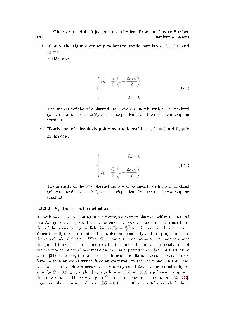
182Chapter 4. Spin injection into Vertical External Cavity Surface
Emitting Lasers
B) If only the right circularly polarized mode oscillates, IR 6= 0 and
IG = 0:
In this case:
IR =
G
β
(1 +
∆GN2
)
IL = 0
(4.43)
The intensity of the σ+-polarized mode evolves linearly with the normalizedgain circular dichroism ∆GN and is independent from the non-linear couplingconstant
C) If only the left circularly polarized mode oscillates, IR = 0 and IG 6= 0:
In this case:
IR = 0
IL =G
β
(1− ∆GN
2
) (4.44)
The intensity of the σ−-polarized mode evolves linearly with the normalizedgain circular dichroism ∆GN and is independent from the non-linear couplingconstant
4.5.3.2 Synthesis and conclusions
As both modes are oscillating in the cavity, we have to place ourself in the generalcase A. Figure 4.24 represent the evolution of the two eigenstate intensities as a func-tion of the normalized gain dichroism ∆GN = ∆G
Gfor dierent coupling constant.
When C = 0, the modes intensities evolve independently and are proportional tothe gain circular dichroism. When C increases, the oscillation of one mode saturatesthe gain of the other one leading to a limited range of simultaneous oscillations ofthe two modes. When C becomes close to 1, as expected in our 1
2 -VCSEL structurewhere [343] C ' 0.9, the range of simultaneous oscillations becomes very narrowfavoring then an easier switch from an eigenstate to the other one. In this case,a polarization switch can occur even for a very small ∆G. As presented in gure4.24, for C = 0.9, a normalized gain dichroism of about 10% is sucient to tip overthe polarizations. The average gain G of such a structure being around 1% [333],a gain circular dichroism of about ∆G = 0.1% is sucient to fully switch the laser

4.5. Optically spin-injected VECSELs 183
Range of simultaneous oscillations
Our structure
Figure 4.24: Intensities evolution of the two eigen-polarization as a function of the
normalized gain dichroism for three values of coupling constant C: 0, 0.5 and 0.9.
polarization thanks to the leverage eect of the non-linear coupling constant.
We can now roughly estimate the eective spin injection in the 12 -VCSEL QWs
using the measured threshold reduction values (Inset Figure 4.22). Averaging be-tween the threshold reduction for the σ+- and σ−- modes enables to minimize theimpact of the cavity geometry on the modes selection. Doing so we nd an averagethreshold reduction for the optically spin-injected VECSEL of 3.55%. But we alsoknow from the rates equations simulation performed by Holub & Bhattacharya onGaAs/AlGaAs-MQW VCSEL [84] (section 2.2.3.2) that the limit case of a 100%spin-polarized carriers induces a maximum threshold reduction of 50%. By assum-ing in rst approximation a linear dependence between the injected spin-polarizationand the associated threshold reduction, this average threshold reduction of 3.55%observed in our system corresponds to an eective spin-polarization PS ≈ 7.1% inthe VECSEL QW. This value is an order of magnitude greater than the theoreticalinferior limit (0.1%) required to trigger a polarization switch. Therefore we un-derstand here how such a moderate eective spin-injection generates a polarizationswitch from a circular eigen state to another.
In terms of amplication of the spin information, we clearly see that an eectivespin-injection PS ≈ 7.1% leads to the emission of circularly-polarized modes witha DoCP of 80%. This amplication of the spin-information injected in the laserby a factor of 11 can be attributed to the leverage eect of the non-linear couplingconstant C. This empirical constant accounts for the gain competition between thelaser modes trying to oscillate in the cavity. In our case where C = 0.9, the modeselected at threshold will be the one exhibiting the highest gain. Generally, for a

184Chapter 4. Spin injection into Vertical External Cavity Surface
Emitting Lasers
mode to be selected at threshold, its associated gain does not need to be extremelyhigh but just higher than those of the other modes.
Finally, we can compare this estimated PS ≈ 7.1% to the gain circular dichro-ism ∆G extracted from the previous birefringence measurements of the same 1
2 -VCSEL (GaAs615). We remind that a ∆GN ≈ 4% corresponding to a net gaincircular dichroism ∆G ≈ 0.4% (assuming G = 1%) was shown to be an inferiorlimit required to simply compensate the average linear birefringence. For the value∆G ≈ 0.4% , the VECSEL is set in an articial isotropic state for the TE- andTM-modes and both modes are supposed to still be linearly-polarized and orientedat 45 from the ordinary [011] and extraordinary [011] axis (section 4.4). The esti-mated eective spin-polarization in the VECSEL's QW PS ≈ 7.1% is greater thanthis minimum value ∆G ≈ 0.4% required to compensate the birefringence in thestructure. Consequently, this value of PS should be sucient to overpower the linearbirefringence and set a circularly-polarized emission. However, in the rst opticalspin-injection experiment (linear cavity, no Faraday rotator) no inuence of the spin-injection could be seen on the modes polarization even if the VECSEL was opticallyspin-injected with an approximately similar eciency. The same observation wasalso made in the second experiment after withdrawing the Faraday rotator from theM-Cavity. We conclude that although the eective spin-polarization injected in theVECSEL compensates the linear birefringence, the laser might still be just above thecompensation point (1
4∆G2N = sin2 γ′
2 ) and PS is not high enough to even triggeroscillations on elliptically-polarized modes. This locking of the laser on linearly-polarized modes might also be favored by an additional residual linear birefringenceoriginating from the cold cavity. Indeed, contrary to the short linear cavity used toperform the birefringence measurements, this extended M-cavity is composed of fouradditional mirrors each of them introducing a residual birefringence. Consequently,we can make the hypothesis that the eective spin-injection required to compensatethe total linear birefringence of the M-Cavity VECSEL might be sensibly higherthan in the previous birefringence experiment from where the value ∆G ≈ 0.4%has been extracted. As predicted by the vectorial model (section 4.3.2), the impor-tance of the intra-cavity Faraday rotator is thus clearly highlighted. The emissionof circularly-polarized modes with a DoCP of 80% shows how the circular birefrin-gence articially introduced by the Faraday rotator compensate the intrinsic linearbirefringence of the 1
2 -VCSEL and enable us to reveal the inuence of the injectedspin-polarized carriers on the modes polarization.
One has to note that the DoCP measurement of 80% reported here has been per-formed on a carefully chosen operating point on the 1
2 -VCSEL surface, for a 100µm pump spot and for a given pumping power. Just like monolithic VCSELs, 1
2 -VCSELs exhibit local strain variations between dierent regions of the structure andthus local variation of birefringence γ. As shown by the Spin-Flip Model in the caseof two linearly polarized mode (section 2.2.3.3), for a given linewidth enhancementfactor α of the semiconductor laser, polarization switching can occur for variation

4.5. Optically spin-injected VECSELs 185
of pumping power and birefringence. One can note that the intrinsic birefringenceγ is a xed characteristic of a given VECSEL structure and is though independentof the optical pumping. Nevertheless, as witnessed during the birefringence mea-surements (section 4.4), a pump induced birefringence also inuences the dynamicalbehavior of the device (Thermal eects). To summarize, the spin-injected VECSELis a system highly sensitive to small perturbations. By changing the pump parame-ters (power and/or spot size), the operating point on the 1
2 -VCSEL surface but alsothe VECSEL temperature, the measured DoCP would have been either higher orlower. Complementary systematic studies focusing on: (i) the inuence of the pumpparameters and (ii) the inuence of the external cold-cavity shape would provideinteresting additional insights on the VECSEL behavior under spin-injection.
In any case, this experiment highlights the fundamental dierence between spin-injection in LED and spin-injection in VECSEL. In this section, we showed how aspin-injection of 7.1% in VECSEL leads to an output DoCP of 80% with a completepolarization switch at room temperature while in a Spin-LED an input PS of 7.1%would give at best an output DoCP of 7.1%. Once the VECSEL oscillates on acircularly-polarized eigen state, the system has by default a high DoCP. The strongnon-linear coupling between the two circularly polarized modes favors the polariza-tion switch despite the generation of a very low net gain circular dichroism in thelaser (⇔ a very low eective spin injection in the active medium). Consequently,even if the spin-injection mechanism is not highly ecient due to the combination ofseveral spin-relaxation mechanisms, one can still obtain a polarization switch witha high DoCP for both circularly polarized modes at room temperature.

186Chapter 4. Spin injection into Vertical External Cavity Surface
Emitting Lasers
4.6 Discussion on the characteristic lifetimes
A side from the colossal inuence of the non-linear amplication eects on the po-larization selection of the VECSEL, we still need to understand why an intra-cavityFaraday rotator is required to prepare laser oscillations on circularly polarized eigenmode. Indeed other groups working with monolithic VCSEL successfully reportedpolarization manipulation using spin injection without any need of a non-reciprocalmaterial in the laser cavity. As discussed in the vectorial model (section 4.3), theinuence of the ratio between the linear birefringence and the gain circular dichro-ism is indisputable but to push further the understanding of the system, one has topay interest to the ratio between the carrier lifetime τ and the spin lifetime τs inthe VECSEL. These two parameters x the average spin population imbalance inthe structure and consequently the gain circular dichroism. The importance of theratio between the carrier lifetime τ and the spin lifetime τs in the active medium ofspin-optoelectronic devices has already been introduced in the state-of-the-art (sec-tion 2.2.1.2). This has been highlighted in the previous chapter during the studyfocusing on the optimization of the electrical MTJ spin-injector using Spin-LED.
As opposition with Spin-LED where τr stays relatively constant as the device onlyemits in a spontaneous emission regime, the carrier lifetime in VECSEL and inlasers in general, strongly depends on the operation regime. In our VECSEL thecarrier lifetime is mainly radiative under the chosen experimental operation condi-tions. The radiative lifetime of an excited electronic state in the gain medium of thelaser is the lifetime which would be obtained if radiative decay via the unavoidablespontaneous emission were the only mechanism for depopulating this state [347].Depending on the pumping rate η and the operation regime, the radiative lifetimecan change by one or sometimes two orders of magnitude. This has a strong impacton the ratio between τ and τs and consequently on the laser output DoCP.
4.6.1 Radiative lifetime dynamics in a laser
In a laser the global recombination of the excited carriers can be divided in two cat-egories. The radiative recombination generating spontaneous or stimulated photonsdepending on the operation regime of the laser and the non-radiative recombinationsource of phonons and lattice vibrations. In CW pumping and stationary regime, thedierent types of recombination mechanisms occurring in the laser's active mediumare linked by:
R = A ·N +B ·N2 + C ·N3 (4.45)
where R is the total recombination rate and N is the carrier density in theQW. The coecient A is the trap and surfaces recombination coecient accountingessentially for recombination on defects (Electrons lifetime on defects: vacancy,

4.6. Discussion on the characteristic lifetimes 187
impurities,...). B represents the radiative bi-molecular recombination coecient(e− − h+) while C is the non-radiative Auger coecient. The recombination timeτr can then be derived from (4.45):
τr =1
A+B ·N + C ·N2(4.46)
We also dene the radiative quantum yield ηi quantifying the conversion rate ofthe carrier density into radiative recombination:
ηi =BN
A+B ·N + C ·N2(4.47)
Dierent orders of magnitude for τr can then be distinguished depending on theoperation regime of the laser:
• Below threshold, Spontaneous emission regime: For a low pump den-sity, N Ntrans, where Ntrans is the carrier density at transparency. Thisleads to BN A =⇒ ηi 1. In the spontaneous emission regime, the aver-age carrier lifetime is completely dominated by spontaneous recombination andone can expect a carriers' non-radiative lifetime of around: τnon−radiative ≈[5-50] ns at room temperature. The non-radiative lifetime is directly proportionalto the defect density of the structure. The better the crystalline quality, thelonger the non-radiative carrier lifetime will be.
• Above threshold, Stimulated emission regime (moderate pumping):
When the pump density is above threshold, N ≈ Ntrans. At transparency, theFermi levels start to be tangential to the bands and everything absorbed isre-emitted. This leads to BN > A =⇒ ηi 7→ 1. In the stimulated emissionregime the carrier lifetime is drastically reduced and mainly limited by thecarrier relaxation time from the pump level to the lasing level τr ≈ 50 ps,which is much shorter than the spin lifetime at room temperature [228]. Inthe case of a moderate pumping, when staying close to threshold, the numberof electrons lost by Auger recombination remains tolerable and the quantumyield ηi is high enough to ensure laser operation (B ·N > C ·N2).
• Above threshold, Auger regime (very high pumping): In this casemost of the excited electrons are lost on non-radiative Auger recombinations:B ·N << C ·N2 =⇒ ηi 7→ 0. In this regime the stimulated emission breaksdown and the laser stops emitting. However, in the case of V(E)CSEL, thelaser usually stops emitting when increasing the pumping several time abovethreshold as the system faces a thermal roll-over before the Auger regime.

188Chapter 4. Spin injection into Vertical External Cavity Surface
Emitting Lasers
Figure 4.25: Evolu-
tion of the carrier life-
time τr as a function of
the pumping rate η in
the stimulated emission
regime for the VECSEL
GaAs615. η = 1 denes
the threshold.
0.01 0.1 1 10 0.1
10
1
η-1
Car
rier
s L
ifet
ime τ r
(n
s)
Figure 4.25 illustrates the variation of the electron lifetime (essentially radiativeabove threshold) in the QW as a function of the pumping rate for the structureGaAs615 in the stimulated emission regime. η = 1 denes the threshold. Belowthreshold in the spontaneous emission regime and close to threshold the carrierlifetime is expected around 2-3 ns. This prediction is coherent with carrier life-time measured in similar VECSEL that where experimentally estimated aroundτradiative ≈[2-3] ns above but close threshold [333]. In these structures the radiativequantum yield is around ηi = 80%. When the pumping rate increases, τr startsdecreasing and a carrier lifetime as low as 200 ps could be expected 8 times abovethreshold. A spin lifetime of around 10 ps can be reasonably expected in such In-GaAs QW at room temperature [348]. Consequently, combined with the non-linearamplication eects, such a spin-lifetime might provide a sucient gain circulardichroism to compensate the residual linear birefringence of the system and lock thelaser on circularly polarized eigen states.
According to the evolution of the carrier lifetime as a function of the pumpingrate, the best solution to optimize the τr
τs-ratio would intuitively appear to push the
pumping several time above threshold. Unfortunately this action would also bringinto play spin-depolarizing mechanisms. When increasing the excitation power, elec-trons with greater wave vector ~k are engaged in the recombination process. Thoseinitially spin-polarized electrons of higher energy E(~k) relax through the Dyakonov-Perel mechanism at a much faster rate. Additionally, in the case of optical pumpingimportant thermal gradients rise in the structure and can potentially have a neg-ative inuence on the spin lifetime. It directly causes important lattice vibrationand phonon generation in favor of the Elliot-Yafet spin-relaxation mechanism whichconsiderably reduces the spin-lifetime: τs ∼= τEYsf (T ) ∝ τp(T )
T 2 . Additionally, thermalstrains on the active medium can potentially increase the eective total birefrin-gence of the structure and compensate the gain circular dichroism generated byspin injection in favor of linearly-polarized eigen modes. As for optical pumping,under high electrical pumping thermal eects could reduce τs in the 1
2 -VCSEL's QWthrough the DP- and EY-mechanism. In short, the situation is non-trivial and a

4.6. Discussion on the characteristic lifetimes 189
balance has to be found between maximizing the spin lifetime and the minimizingthe carrier lifetime. Experimentally, this optimum functioning point is dicult tond in dynamics operation.
With TRPL measurement we measured the carrier lifetime τr and the spin lifetimeτs of our VECSEL structure design for optical pumping. These extracted charac-teristic lifetime are then compared with state-of-the-art measurements achieved onmonolithic Spin-VCSEL.
4.6.2 Time-Resolved Photo-Luminescence measurements
The study of the carrier lifetime τ and the spin lifetime τs in the VECSEL is per-formed by Time Resolved Photo-Luminescence (TRPL) using a pulsed Ti:Sa laserwith a pulsed width of 1.5 ps and a repetition rate of 80 MHz, combined with astreak camera (S1-Photocathode) for the detection. The temporal resolution of thestreak camera depends on the selected time range. A temporal resolution of 17ps is chosen for the measurements performed on the VECSEL. The objective is toextract precise measurements of τ and τs in order to estimate the eective averagepercentage of spin polarized electron recombining in the QW.
The measurements on the In20%Ga80%As/GaAs95%P5% QW used as the active mediumof the VECSEL are performed by varying several experimental parameters such asthe excitation energy of the photon (excitation within the barriers or intra-QW),the power regime and the temperature. Measurements were realized at both low(10 K) and room temperature (300K) and for an average excitation power (PT i:Sa)ranging from 1 µW up to 10 mW with a 50 µm-diameter spot. This gives a peakpower range between 8 mW and 80 W (Ppeak = PTi:Sa×12ns
1.5ps ). Excitation powers arekept relatively low in order to mainly explore the spontaneous regime.
First, k.p simulations considering a 8-bands structure (2 CBs - 2 HH-Bands - 2LH-Bands - 2 Split-O Bands) in In20%Ga80%As/GaAs95%P5% QW were performedusing the approximation of innite thickness barriers to estimate the values of thedierent optical transitions [349]. Figure 4.26 schematizes the band diagram derivesfrom the simulation. This preliminary step was necessary in order to identify thedierent excitation energies required to target specic band-to-band transitions andthen calibrate the Ti : Sa laser accordingly. Complementary information on theexperimental setup, the band-to-band transition energies and the dierent Ti : Sa
wavelengths used to performed the TRPL measurements can be found in AppendixE, Section E.1 and E.2.
The results of the TRPL measurements performed on the GaAs615 VECSELwith In20%Ga80%As/GaAs95%P5% QW are display below. Dierent cases corre-sponding to dierent experimental conditions are reported. In every cases, theexcitation light emitted by the Ti:Sa laser is circularly polarized (σ+ or σ−) and thedetection system is congured to detect circularly polarized light. The DoCP of the

190Chapter 4. Spin injection into Vertical External Cavity Surface
Emitting Lasers
Figure 4.26:
Schematic represen-
tation of the In-
GaAs/GaAsP QW
band structure with the
associated transition
energies extracted from
k.p simulations in the
approximation of innite
thickness barriers [349].
135 meV
e1
e2
38 meV
129 meV
22 meV lh
93 meV
hh
114 meV
hh1 hh2 hh3
9 meV 35meV
76meV
Eg=1,214 meV
lh1
e
28 nm
GaAs95%P5%
8 nm
In20%Ga80%As
CB
VB
28 nm
GaAs95%P5%
VECSEL emission can then be calculated from the measured Iσ+ and Iσ− intensi-
ties: DoCP =∣∣∣ Iσ+−Iσ−Iσ++Iσ−
∣∣∣. A control experiment was primarily performed by exciting
the system with linearly-polarized light to ensure that the measurements were notbiased. A weak artifact DoCP of -1% was measured witnessing a good alignmentof the experimental setup (see Figure 4.27 (b)). Note that in a 1
2 -VCSEL designedfor electrical pumping, one has to take into account the internal electric eld dueto the p − i − n junction. This eld can be screened depending on the density ofphoto-generated carriers and this may have an inuence on the characteristic relax-ation time. In our case this problem is ruled out as we study a 1
2 -VCSEL designedfor optical pumping with no p-i-n junction. For clarity and presentation reasons Ipersonally chose not to include here every graph related to every single measure-ments. The curious reader is cordially invited to refer to Appendix E, section E.3,for complementary information.
A) Low temperature measurements (10 K):
1. Carrier lifetime measurements:
i. Non-resonant excitation above the GaAsP Barriers:
The excitation energy is chosen above the gaps of GaAs and GaAsPET i:Sa = 1.589 eV corresponding to a wavelength of λT i:Sa = 780 nm.In these experimental conditions, the measured carrier lifetime τ is inthe range of [410±20ps−550±20ps] for the range of excitation powerPT i:Sa comprise between [1µW−100µW ]. We observe a longer risingtime for the luminescence in the rst pico-seconds when increasingthe excitation power. Indeed, the number of carrier generated in theGaAsP barriers increase as well as the average diusion time towardthe QW where radiative recombinations occur.
ii. Intra-QW excitation below e1− lh1 transition energy:

4.6. Discussion on the characteristic lifetimes 191
0 500 1000 1500 20000.01
0.1
1 T = 10 K
N
orm
alized
PL
in
ten
sit
y
Delay (ps)
exc
=780nm ; P=1 W ; = 410±5ps
exc
=780nm ; P=100 W ; = 550±5ps
exc
=880nm ; P=100 W ; = 680±5ps
exc
=900nm ; P=100 W ; =670±5ps
0 200 400 600 800 1000 1200 1400 1600
0
10
20
30
40
T = 10 K
Do
CP
(%
)
Delay (ps)
Circular Excitation, P = 100µW:
Intra-well ; exc
= 900nm ; s = 120±20ps
Intra-well ; exc
= 880nm ; s = 135±20ps
Non-resonant ; exc
= 780nm ; s = 103±20ps
Control experiment: Linear excitation,
P = 100µW, intra-well
(a) (b)
Figure 4.27: Time Resolved Carrier lifetime and Spin lifetime measure-
ments comparison: (a) Carrier lifetime measurements at T=10 K for non-resonant
(780 nm) and (880 - 900 nm) intra-well pumping with dierent excitation powers of
the VECSEL structure. (b) Spin lifetime measurements at T=10 K for non-resonant
(780 nm) and (880 - 900 nm) intra-well pumping under an excitation power of 100
µW. Note that the photo-generated carriers densities are very dierent in these two
modes of excitation due to the strong dierence in light absorption. The control ex-
periment under linearly-polarized excitation ensures that the measurements are not
biased (DoCP≈0%).
In this case, the excitation energy ET i:Sa = 1.424 eV correspondingto a wavelength of λT i:Sa = 870 nm is chosen to trig an excitationbelow e1 − lh1 transition energy. Therefore the active transitionsin this measurements are mainly between the CB and the HH-band(Figure 4.26):
• When λT i:Sa is xed at 870nm: The carrier lifetime τ varieslittle with the excitation power when the latter is kept relativelylow. When increasing the excitation power from 0.3 mW upto 1 mW, τ only changes by 5 ps which stays in the error barof the measurement setup giving an estimated carrier lifetime ofτ = 685±20 ps on this power range (see gure E.2 in Appendix E,section E.3). However, when the excitation power increases up to3 mW and then 10 mW, the carrier lifetime signicantly increasesas well to τ = 875±20 ps and τ = 900±20 ps respectively (gureE.2 in Appendix 5, section E.3).
• When PT i:Sa is xed to 100 µW (⇔ Ppeak = 800 mW): Mea-surements were also performed to evaluate the dependance of thecarrier lifetime on the excitation wavelength λexc. By slightlytuning λexc from 880 nm (⇔ ET i:Sa = 1.408 eV) to 900 nm (⇔ET i:Sa = 1.377 eV), τ was seen to sensibly decrease from 680±20
ps to 670±20 ps. This highlight the weak dependance of the car-rier lifetime on λexc, at least for a low excitation power (Figure4.27 (a)).

192Chapter 4. Spin injection into Vertical External Cavity Surface
Emitting Lasers
Comments: To summarize, whatever the excitation conditions are (intra-QW or non-resonant in the barriers, excitation power range), the carrierlifetime measured at 10 K is below 1 ns in the window τ ∈ [410 − 900]
ps. Let's note that at low temperature (10 K) the emission is mainlydue to the heavy-exciton (bounded e− − h+ pairs due to the Coulombinteraction) line. However, as the excitation is non-resonant with thisline, the luminescence dynamics is controlled by a complex mixing of freeelectron-Heavy Hole pairs and heavy excitons. The characteristic decaytime of the photo-luminescence can be seen in rst approximation as aneective electron lifetime.
2. Spin lifetime measurements:
One has to keep in mind that at 10 K we detect the luminescence ofthe heavy-exciton line. However, as we do not perform strictly resonantexcitation of this line, the hole spin relaxation is very fast (few ps). Ac-cordingly, we can consider that the decay of the circular polarization rateis controlled by the electron spin lifetime.
i. Non-resonant excitation above the GaAsP Barriers:
The excitation energy is chosen above the gaps of GaAs and GaAsPET i:Sa = 1.589 eV corresponding to a wavelength of λT i:Sa = 780 nm.The DoCP and the spin lifetime are measured for PT i:Sa = 100 µWand we nd an initial DoCP ≈ 8.5% with τs = 105 ± 15 ps (Figure13.3 (b)). For a range of excitation power PT i:Sa ∈ [1µW − 100µW ],we nd that the initial DoCP and the initial τs are decreasing withpower and are respectively in the windows [8.5%−17.5%] and [103±20ps− 170± 20ps].
ii. Intra-QWs excitation:
Here, the excitation is kept intra-well while slightly tuning the exci-tation wavelength to evaluate the spin lifetime dependency on λexc.For these measurements, the excitation power is xed to PT i:Sa = 100
µW. First, a control experiment was performed by exciting the sys-tem with linearly-polarized light and detecting the emitted DoCP toensure that the measurements were not biased. Doing so, a neglect-ful artifact DoCP of -1% was identied witnessing a good alignmentof the experimental setup (see Figure 4.27 (b)). Then, for an ex-citation at λT i:Sa = 880 nm (ET i:Sa = 1.408 eV), the recorded ini-tial DoCP reaches approximately 28% with a spin lifetime estimatedaround τs = 135± 15 ps, while for an excitation at λT i:Sa = 900 nm(ET i:Sa = 1.377 eV) the initial DoCP increases up to 38% and themeasured spin lifetime decreases down to τs = 120 ± 15 ps (Figure4.27 (b)). So, for intra-well excitation, the initial DoCP decreaseswhen the energy of photons increases. It can be explained by themixing between the HH and LH valence bands out of the Γ-point,when e− − h+ pairs are photo-generated with ~k 6= ~0.

4.6. Discussion on the characteristic lifetimes 193
0 200 400 600 800 1000 1200 1400 1600-20
-15
-10
-5
0
5
10
15
20
T = 10 K
exc = 880nm
Pexc
= 100µW
(X -
Y)/
(X +
Y)
Delay (ps)
Excitation: Circular - Detection: Linear
Excitation: Linear - Detection: Linear
Figure 4.28: Mea-
surements of the linear
polarization degree
under linearly- and
circularly-polarized
excitation by detecting
linearly-polarized light
along the [110] and [110]
crystallographic axis.
General comments:
I The measured spin lifetime at 10 K is in the window [103− 170] psdepending on the excitation conditions (photon energy, excitationpower).
I Under non-resonant excitation, the initial DoCP is clearly lower.When electrons are excited in the 28 nm thick GaAsP barriers, whichare thick enough to be consider as a bulk like material, the maximumphoto-generated spin-polarization achievable is only 50% (and not100% as the in QW) due to the optical selection rules [168]. Sub-sequently, when these electrons diuse from the barrier toward theQW, they induce a decrease of the average spin-polarization in theactive medium of the VECSEL and consequently reduce the emittedDoCP. It is important to note that this mechanism is hosted by theVECSEL during laser operation. The broad pumping at 808 nm ex-cite the GaAsP barriers as well as both the HH−CB and LH−CBtransitions leading to a maximum achievable spin-polarization of 50%in the QW.
I Degree of Linear Polarization: An additional experiment was
performed to identify the Degree of Linear polarization(DoLP =
IσX−I
σY
IσX
+IσY
)under both linearly- and circularly- polarized excitation. The de-tection axis X and Y are chosen along crystallographic axis [110]and [110] respectively. The excitation energy is chosen intra-well atET i:Sa = 1.408 eV corresponding to a wavelength of λT i:Sa = 880
nm and the average excitation power is xed to PT i:Sa = 100 µW.For both type of excitation, the linear polarized emission was foundto be very minor (Figure 4.28). A DoLP of ≈ 0% and ≈ 1.5% weremeasured under circularly-polarized excitation and linearly-polarized

194Chapter 4. Spin injection into Vertical External Cavity Surface
Emitting Lasers
0 5 10 15 20 25 30 35 40 45 500.0
0.2
0.4
0.6
0.8
1.0
Linear Scale
No
rmal
ized
PL
inte
nsi
ty
Delay (ns)
0.0 0.2 0.4 0.6 0.8 1.0 1.2 1.4 1.6 1.8 2.0
0
2000
4000
6000
8000
10000
12000
Photoluminescence
s < 100 ps
Intra-well Circular Excitation, exc
= 965nm, Pexc
= 1mW
PL
In
ten
sit
y (
a.u
.)
Delay (ns)
-5
0
5
10
15
20
25
30
35
40
DoCP
Do
CP
(%
)
0 5 10 15 20 25 30 35 40 45 500.01
0.1
1
0 5 10 15 20 25 30 35 40 45 500.0
0.2
0.4
0.6
0.8
1.0
Linear Scale
No
rma
lize
d P
L i
nte
ns
ity
Delay (ns)
T = 300 K
Pexc
= 1 mW
exc
= 965 nm
1
2
det
=985nm ; 1=5.6±0.2ns ;
2=22±3ns
No
rma
lize
d P
L i
nte
ns
ity
Delay (ns)
(a) (b)
Figure 4.29: Time Resolved Carrier and Spin lifetimes measurements: (a)
Carrier lifetime measurement at T=300 K for resonant pumping with an excitation
power of 1 mW at 965 nm. The inset shows the same data plotted on a linear scale.
(b) Polarization dynamics at T=300 K for resonant pumping with an excitation power
of 1 mW at 965 nm.
excitation respectively. Unfortunately, as we are not able to exciteand detect strictly resonant with the heavy-exciton (XH) due tothe use of the streak camera, these experiments do not allow us toconclude that the eigenstates are not linearly polarized and that thelinear birefringence of the structure is not due to the QW themself.
B) Room temperature measurements (300 K) under Intra-QW excita-
tion below e1− lh1 transition energy:
The same carrier lifetime measurements were then performed at 300 K forλT i:Sa = 965 nm. Preliminary runs revealed signicantly longer carrier life-times compare to the 10 K measurements. Consequently, to avoid issues linkedto long relaxation time, the experimental setup had to be modied. A pulsepicker was installed on the laser chain in order to bring the repetition ratedown to 4 MHz and allow a good evacuation of the excited carriers before anyre-excitation. Additionally, a triggering module was mounted on the streakcamera. With this setup, the camera's detection is triggered instead of beingsynchronized with the Ti:Sa emission.
Figure 4.29 (a) shows the PL intensity for an excitation at 965 nm and adetection window centered at 985nm. The measured relaxation of the PL in-tensity can be modeled by a double exponential with a rst short relaxationtime τ1 of ≈5 ns and a second longer relaxation time τ2 of ≈20 ns. Mostof the photons are emitted during the rst 10-15 ns. Consequently, the rstrelaxation time τ1 gives a better image of the dynamics of the real systemand is the one that should be considered when comparing the carrier lifetimeto the spin lifetime in CW experiments. Preliminary test to measure circularpolarization dynamics seems to indicate that the spin relaxation time is below

4.6. Discussion on the characteristic lifetimes 195
100 ps (Figure 4.29 (b)).
4.6.3 Data comparison and partial conclusion
Table 4.1 summarizes the values of τr et τs extracted from the TRPL measurementwith other measurements performed in V(E)CSEL structures with dierent activemedium at various temperatures. To this day, only few formal studies of the spinlifetime in VCSEL have been reported. In general, it is quite challenging to preciselydescribe the behavior of the characteristic lifetimes as they are strongly dependenton several experimental parameters namely the temperature, the nature of the ac-tive medium (doping, number of QWs, QWs width,...) and especially the operationregime.
At 300 K, the carrier lifetime is estimated around τ = 5 ns for an excitation powerof PT i:Sa = 1 mW. This measurement is coherent with the value of τ previouslyreported on similar VECSEL close to threshold using a dierent experimental ap-proach [333]. The extracted spin lifetime tend to be smaller than the low tempera-ture values reported in the literature for similar active mediums. At 10K, τs is of theorder of magnitude of ≈ 100 ps for both resonant and non-resonant pumping. At300K, rst measurements seems to indicate that τs is below 100 ps. To my knowl-edge, no spin lifetime measurements has expressly been performed on (100)-QWVCSEL at room temperature. The only room temperature data was disclosed byFujino et al. with a τs = 440 ps in (110)-GaAs QW VCSEL [283]. This spin lifetimecan not be used for a direct comparison as a [110] growth direction of GaAs can-cels the Dyakonov-Perel mechanism and considerably increase the spin relaxationtime [193, 350, 351].
Under optical pumping (λexc = 808 nm) in real operation conditions, carriersare also excited in GaAsP barriers and GaAs spacers. However, while the GaAsPcarriers diuse and recombine in the QW, the 28 nm thick GaAsP barriers providea good shielding against the diusion of GaAs spacers's carriers in the QW. Never-theless as the QWs absorption is only about 1%, pumping in the barriers is neededto push the VECSEL in the stimulated emission regime.
The main limitation in order to compare the results obtained with our VECSELunder continuous wave excitation at 300 K and by TRPL at 300 K on the 1
2 -VCSELare: (i) the dierent operation regimes (Stimulates Vs. Spontaneous respectively)and (ii) the excitation energy (above the GaAsP barriers Vs. intra-well belowe1 − hh1 exciton respectively). Complementary measurements will be led at theLPCNO to perform TRPL under experimental conditions closer to those used forCW laser operation under optical pumping.
Oestreich et al. studied in detail the threshold reduction dependence on the spinrelaxation time of an electrically pumped commercial VCSEL (Inneon Technology)using simulation based on the analytical model presented in section (2.2.3.2) [232].For a theoretical 100% spin-injection eciency, they showed a strong decrease of

196Chapter 4. Spin injection into Vertical External Cavity Surface
Emitting Lasers
Active Medium Carrier lifetime τr Spin lifetime τs Reference
(100)-GaAs QW Low pumping rate: ≈ ns 100 ps [228]
High pumping rate: 50 ps
(100)-GaAs QW τcapture=20 ps - [84]
InAs/GaAs QD 100 ps @ RT 6 ps @ RT [235]
(100)-InGaAs QW τcapture=45 ps Barriers: 500 ps [37]
QWs: 300 ps
(110)-GaAs QW 420 ps @ 77 K 2.8 ns @ 77 K [283]
440 ps @ RT
(100)-GaAs QW 40 ps @ RT 230 ps @ 70 K [283]
(100)-InGaAs QW ≈ ns @ RT [333]
(100)-InGaAs QW - 100 ps @ 15 K [282]
- - 1-13 ps @ RT [273]
- - 10 ps @ RT [?]
10 K, non-resonant, 10 K, non-resonant,
1 µW, λexc = 780 nm 1 µW, λexc = 780 nm
→ τr=410 ps → τs=170 ps
10 K, non-resonant, 10 K, non-resonant,
100 µW, λexc = 780 nm 100 µW, λexc = 780 nm
→ τr=550 ps → τs=105 ps
(100)-InGaAs QW 10 K, intra-well, 10 K, intra-well, TRPL
(our sample) 100 µW, λexc = 870 nm 100 µW, λexc = 880 nm
→ τr=680 ps → τs=135 ps
10 K, intra-well,
10 mW, λexc = 870 nm
→ τr=900 ps -
300 K, intra-well 300 K, intra-well
1 mW, λexc = 965 nm 1 mW, λexc = 965 nm
→ τr ≈5 ns → τs < 100 ps
Table 4.1: Comparison of state-of-the-art carrier lifetime and spin lifetime measure-
ments of V(E)CSEL structures with dierent active medium at various temperatures.
the laser threshold when τs increases from 50 ps to 200 ps and they also comparedthe room-temperature "spin-performances" of various QW-based active mediums(Figure 4.30). Spin relaxation times of few ps and about 50 ps are typical for un-doped InGaAs QW and bulk GaAs, respectively. Consequently, one should notexpect a signicant threshold reduction of the V(E)CSEL when using these ma-terial as an active medium. With the active medium of our 1
2 -VCSEL made of12 In20%Ga80%As/GaAs95%P5%-QW, we have observed a low threshold reduction of

4.6. Discussion on the characteristic lifetimes 197
.
Figure 4.30: Simulation of the threshold evolution of a commercial VCSEL
at room temperature: Left axis: Evolution of the laser threshold as a function of
the spin relaxation time (Black line). Right axis: Percentage of threshold reduction
as a function of the spin relaxation time. Top axis: Spin relaxation time of several
semiconductor systems. The estimated long spin relaxation time for the 15 nm co-
doped (001)-GaAs QW has not been experimentally conrmed yet. The experimental
parameters used for the simulation can be nd in [232]. Figure reprinted from [232]
few percents in agreement with preliminary measurements of τs below 100 ps. In 7.5nm wide co-doped (001)-GaAs QW spin relaxation times of about 100 ps have beenmeasured at room temperature [352]. These relatively long spin relaxation times re-sult from motional narrowing due to fast momentum scattering at the co-doping andshould yield a threshold reduction of about 20%. Even longer spin relaxation timesof a few hundred ps are expected in wider co-doped (001)-GaAs QW. The relevantDyakonov-Perel spin relaxation mechanism decreases when quantization energy de-creases, leading to a laser threshold reduction of about 40%. As supported by theexperimental results of Fujino et al. [283], changing the growth direction of GaAsQW from [001] to [110] increases the spin relaxation times up to the nanosecondregime as the Dyakonov-Perel mechanism is canceled for electrons spin-polarizedalong the growth direction [193]. For such systems the expected threshold reductionapproaches the limit value of 50%. A similar reduction is in principle expected forwide band-gap semiconductors like ZnSe with a weak spin-orbit interaction [353].

198Chapter 4. Spin injection into Vertical External Cavity Surface
Emitting Lasers
4.7 Electrically spin-injected VECSELs
In an electrically pumped, commercial monolithic GaAs/AlGaAs-QW VCSEL, theminimum transport time of an electron from the contact to the laser gain mediumis estimated around 10 ns [232]. However, the spin relaxation time of the electronin GaAs is about 50 ps at room temperature. Consequently, the spin-polarizationin the gain medium of the laser is close to zero. Side contacts are not a practicalway to shorten the transport time into the active medium of the laser as typicalsmall-area VCSEL still have diameters exceeding 5 µm. At rst sight, one couldconclude that metallic spin injectors are not a practical option for a Spin-VCSELimplementation.
Nonetheless, from the electrical injection viewpoint, the use of 1/2-VCSELs oerthe unique advantage to deposit a spin-injector on top of the structure as close aspossible to the QW. Using this technique maximizes the spin polarization degreereaching the active medium by taking advantage of a spin diusion length lsf longerthan the distance between the injector and the QW. In GaAs, typical lsf valuesare given around [8] 6 µm at 50 K while in our structure the distance betweenthe spin polarizer and the rst QW is about 180 nm. In the active zone, the spinpolarization level will then be governed by the ratio between the spin lifetime τsand the radiation lifetime τr in the QW. Typical values of spin relaxation timeare estimated around [354] τs = 60 ps at Room Temperature (RT) for GaAs QWwhile the radiative lifetime for high excitation (gain regime) far from threshold isgiven around [228] τr ' 100 ps at RT. The ultimate goal of this work is to studyelectrically injected Spin-VECSEL. Nevertheless, given the technological challenges,we rst started by studying the structure under optical spin-injection. As a rstresult, we demonstrate laser oscillations under unpolarized optical pumping despitethe insertion of a non-transparent ferromagnetic spin-injector in the laser cavity.
4.7.1 Insertion of an Intra-Cavity spin-injector
We validated the concept of electrically spin-injected VECSEL by demonstratinglaser oscillations with an optically pumped 1/2-VCSEL incorporating an intra-cavity (2.6nm)MgO/(1.8nm)Co/(3nm)Pt) MTJ ferromagnetic spin-injector within-plane magnetization (Figure 4.31(b)). Thanks to the oxyde barrier, this type ofspin-injector permits to circumvent the impedance mismatch issue [63]. Moreover,the eciency of this architecture has beforehand been proved with Spin-LED [199].We used an antiresonant n.i.d 1/2-VCSEL grown by Metal Organic Chemical Va-por Deposition (MOCVD) consisting in a 27.5-period GaAs/AlAs Bragg mirror(99.9% reectivity). The gain at λ = 1 µm is ensured by twelve strained balancedIn22%Ga78%As/GaAs95%P5% QW in a 13λ/2 cavity. The structure is maintainedat 279 K with a Peltier thermo-electric cooler. The pumping system consists in a808 nm pigtail multimode laser diode delivering up to 2 W and focused on the gainmedium to a 100 µm spot with a 30 incidence angle. The VECSEL is pumped

4.7. Electrically spin-injected VECSELs 199
(a)
f1
f2
Power
Meter
λ = 1000 nm
4.154 mW
M f3 Polarizer L
Peltie
r
VECSEL y
x z
(b)
External Cavity
Intra-Cavity Ferromagnetic Spin-Injector
Output Coupler
(R = 99.5%)
λ = 1 μm
2.6nm MgO / 1.8nmCo / 3nm Pt
y
x
z
Figure 4.31: (a) Experimental setup: We used a linear cavity optically pumped
with a 30 angle. The output optical power emitted by the VECSEL is evalu-
ated using a Power-meter. L = 50mm, f1 = 10mm, f2 = 50mm, f3 = 100mm,
M : (R = 50mm,T = 0.5%) (b) Overview of the VECSEL structure:
The (2.6nm)MgO/(1.8nm)Co/(3nm)Pt MTJ ferromagnetic spin-injector is deposited
intra-cavity, close to the active medium, on a node of the electromagnetic eld.
in the continuous regime throughout the experiment. The linear cavity is closedby a 50 mm radius of curvature concave mirrors with a 0.5% transmission at 1µm(Figure 4.31 (a)). At the output of M the beam is focused on a power-meter (f3)and a polarizer can be inserted to determine the direction and ellipticity of the lightpolarization.
This preliminary experiment was challenging given the high absorption of clas-sical MTJ ferromagnetic spin-injector (typically 10% for 5 nm thickness) comparedto the low optical gain in 1/2-VCSEL (≈ 1%). At λ = 980 nm, the MgO layercan be consider transparent (αMgO = 5.0× 10⁻² cm−1) compared to the Co and Ptmetallic layers (αCo = 7.2458× 105 cm−1 and αPt = 7.3254× 105 cm−1). To over-come this strong limitation, the semiconductor structure was designed so as to placethe spin-injector in one node of the stationary electromagnetic eld. This techniqueenables to minimize the absorption by the ferromagnetic multilayer (FML). Thespin-injector is deposited by sputtering on the surface of the anti-resonant MOCVD1/2-VCSEL (Figure 4.31 (b)). By analyzing the Fourier Transform Infrared Reec-tivity spectra (FTIR) of the system DBR+FML, we see that the FML acts as anarrow frequential pass-band lter on the reectivity (Figure 4.32(b)). The higherthreshold for VECSEL+FML witnesses an increase of losses in the cavity that canbe attributed to surface defects (Figure 4.32(a)). This encouraging result is a rststep toward the realization of an electrically pumped Spin-VECSEL.
4.7.2 Deposition of a spin-injectors with Perpendicular MagneticAnisotropy on a 1
2-VCSEL
In the previous section we successfully demonstrated the feasibility of laser opera-tion despite the insertion of a highly absorbent MTJ spin-injector in the laser cavity.However, this previous accomplishment was realized using a ferromagnetic multi-layer with a magnetization oriented in the plane of the lm. We remind the reader

200Chapter 4. Spin injection into Vertical External Cavity Surface
Emitting Lasers
0 1 2 3 4 5 6 7 8 9 10 11 12 13 14 150
2
4
6
8
10
12
14
16
18
20
= 1 µm
VECSEL
+ Spin-Injector
VECSEL x0.1
VE
CS
EL
Ou
tput
Op
tica
l P
ow
er
(mW
)
Pump Power Density (kW/cm2)
700 800 900 1000 1100 1200
0
20
40
60
80
100
Tra
nsm
issio
n (
%)
Wavelength (nm)
Reference 100%
Glass Slide
GS//2,6nm MgO/1,8nm Co/3nm Pt
Reference 0%
0.80 0.85 0.90 0.95 1.00 1.05 1.10 1.15 1.200.0
0.2
0.4
0.6
0.8
1.0
Reference DBR
DBR//2.6nm MgO/1.8nm Co/3nm Pt
Reflectivity (
a.u
.)
Wavelength (µm)(a) (b)
Figure 4.32: (a) VECSEL output optical power as a function of the pump
power density: The structure with the (2.6nm)MgO/(1.8nm)Co/(3nm)Pt ferro-
magnetic spin-injector is lasing at 279 K despite the losses introduced in the cavity
by the spin-injector. Both measurements have been realized with an output coupler
transmission of T=0.5%. The Inset showcases the spin-injector transmission spectra.
The absorption at 1 µm is around 40%. (b)DBR and DBR+Spin-injector mea-
sured reectivities as a function of the wavelength: the deposition of the FML
strongly inuence the reectivity prole of the bottom DBR. By a careful design we
managed to keep a high reectivity close to the QW Photo-Luminescence (PL) at
λ = 980nm. The energy dierence between the QW gain peak and the DBR resonance
peak (λ = 997nm) can be minimized by adjusting the VECSEL temperature in order
to maximize the output laser power. The shift of the QW PL is about 0.35 nm/K.
that the quantum optical selection rules require an electron's spin-polarization par-allel to the quantization axis of the QW constituting the active medium of the laser.This could of course be achieved by applying a magnetic eld perpendicularly tothe structure in order to drive the spin-injector's magnetization out-of-plane. Un-fortunately, when targeting potential applications, avoiding the requirement of anapplied magnetic eld for operation is non-optional. Consequently, the developmentof an injector exhibiting Perpendicular Magnetic Anisotropy at remanence and atroom temperature on 1/2-VCSEL stood out as the next challenge.
The philosophy of these research was to apply the expertize acquired with the devel-opment of PMA spin-injectors on Spin-LED to the deposition of PMA injectors onthe surface of anti-resonant 1
2 -VCSEL. However even if the technology transfer couldseems trivial at rst sight, several verications and tests needed to be performed inorder to validate and conrmed the feasibility. First of all, the growth methods usedto grow the LED used for optimization and the 1
2 -VCSEL are dierent. The LEDare grown by MBE while the 1
2 -VCSEL are grown by MOCVD which could leadto dierent surface natures and surface qualities. Our study on Spin-LED showedthat the surface quality and the surface preparation before deposition are decisiveparameters for the successful deposition of MTJ spin-injectors with PMA. There-fore, a preliminary verication was to analyze the surface quality of the 1
2 -VCSEL.

4.7. Electrically spin-injected VECSELs 201
-6000 -4000 -2000 0 2000 4000 6000-20
-15
-10
-5
0
5
10
15
20
In-plane
magnetization
M
om
en
t (
em
u)
Magnetic Field (Oe)
ZZ789 as-grown 300K
ZZ789 as-grown 10K
(a)
-6000 -4000 -2000 0 2000 4000 6000-20
-15
-10
-5
0
5
10
15
20
Out-of-plane
magnetization
Mo
me
nt
(e
mu
)
Magnetic Field (Oe)
ZZ789 Annealed 300K
ZZ789 Annealed 10K
(b)
Figure 4.33: Magnetic moment evolution of the system
GaAs763//MgO(2.2nm)/CoFeB(1.2nm)/Ta(5nm) as a function of an applied
magnetic eld at both 10 K and 300 K. (a) Before Rapid Thermal Annealing SQUID
measurements show an in-plane magnetization. (b) After Rapid Thermal Annealing
at 300C for 3 minutes the reconstruction of the CoFeB layer from the MgO/CoFeB
interface induces perpendicular magnetic anisotropy in the multilayer and drive the
magnetization out-of-plane at magnetic remanence.
MOCVD growth provides high quality surfaces with small roughness. An AFManalyze performed on the surface of the GaAs763 electrical 1/2-VCSEL conrmeda good atten surface with a measured roughness of 0.259 nm and a step heightof 3 Angstroms. The surface quality of MOCVD 1
2 -VCSEL and MBE LED is thusquite comparable, which is in favor of a successful technological transfer of the PMAspin-injector onto the surface of 1
2 -VCSEL.
For preliminary electrical testing we decided to rst grow a MgO(2.2nm)/
CoFeB(1.2nm)/Ta(5nm) PMA spin-injector on the electrical structure GaAs763(structure detailed in section 4.2.3) as the distance between the spin-injector and theactive medium has been minimized to approximately 30 nm. The choice was to usethe simplest design to verify: (i) if the structure could lase under electrical pumping,(ii) the possibility of laser operation with an intra-cavity ferromagnetic spin-injectorunder electrical pumping and (iii) to study the spin-injection eciency by analyzingthe DoCP of the light polarization. Nevertheless, contrary to the Spin-LED usedduring the development of this PMA spin-injector, the 1/2-VCSEL required specicsurface preparation before deposition. Indeed, all the LED structures were passi-vated with arsenic after growth inside the III-V MBE chamber. Then, this As capwas desorbed after the LED transfer in the magnetron Sputtering-MBE system usedto grow the injector, right before deposition (section 3.2.1). Here however, the 1/2-VCSEL grown by MOCVD are not capped with a protective As layer which leadsto a thin surface oxidation due to air exposure. First, the surface of the 1/2-VCSELwas chemically etched with HCl for 1 minute and then cleaned with Propan-2-olfor 1 minute. After chemical surface preparation, the second step of the processconsisted in depositing the MgO(2.2nm)/CoFeB(1.2nm)/Ta(5nm) spin-injector

202Chapter 4. Spin injection into Vertical External Cavity Surface
Emitting Lasers
using sputtering growth. This MTJ spin-injector is identical to the one developedon Spin-LED. After deposition, SQUID measurements revealed without surprise thatthe magnetization of the multilayer was in-plane at both 10 K and room temperature(Figure 4.33 (a)). Afterward, a micro-pillar photo-lithography was performed usingthe same process developed for Spin-LED patterning (section 3.1.2). The 1
2 -VCSELpillar is 300 µm in diameter and the two (50nm)Pt/(250 nm)Au contacts on the n-doped surface and one on the p-doped 62.5 nm Zn-GaAs (2.5e17) layer respectivelyare both 110 µm in diameter. To trig a restructuration of the MgO/CoFeB inter-face and induce a perpendicular magnetic anisotropy in the multilayer, the wholeGaAs763//MgO(2.2nm)/CoFeB(1.2nm)/Ta(5nm) structure was annealed usinga Rapid Thermal Annealing (RTA) process of 3 minutes at 300C. Figure 4.33 (b)exhibits the SQUID measurements of the sample after RTA and conrm the out-of-plane magnetization of the spin-injector at remanence at both 10 K and roomtemperature .
To summarize, we demonstrated both the possibility to insert an intra-cavity spin-injector and to grow a spin-injector with PMA on the surface of a MOCVD 1
2 -VCSEL. Combine together, these two properties are highly encouraging toward therealization of an electrically spin-injected VECSEL operating at magnetic rema-nence. By bypassing the requirement of an applied magnetic eld, one could thenenvisage to control the VECSEL polarization using a current line to switch themagnetization's orientation of the spin-injector as in MRAM systems.

Chapter 5
Overall Conclusion
Contents
5.1 Development of a new ultra-thin spin-injector . . . . . . . . 203
5.2 Summary on spin-injection into VECSELs . . . . . . . . . . 204
5.3 Perspectives, challenges and future applications . . . . . . . 208
During this Ph.D thesis, we focused on the study of spin-injection into III-Vsemiconductor based light emitting devices with vertical geometries. This paradigmoers to propagate the information contained in a magnetic bit over really longdistances by converting the associated spin-information into circular polarizationinformation carried by the emitted photons using the optical quantum selectionrules. We paid a particular attention to Spin-VECSELs exhibiting a tremendouspotential for beyond state-of-the-art spin-optoelectronic devices. They oer to com-bine non-volatile magnetic storage of the information in an ultra-thin ferromagneticspin-injector with the potentiality of spin-information propagation over macroscopicdistances. To develop this ambitious and highly multidisciplinary Ph.D subject weperformed various original investigations and experiments in the elds of materialscience, III-V semiconductor physics, spintronics and photonics.
To replace oneself in the general context, this manuscript was divided into threemajor chapters. The second chapter of the manuscipt regrouped a state-of-the-art ofspin-injection into III-V semiconductors optoelectronics devices and focused on thephysical phenomena engaged in the conversion of a spin accumulation into light po-larization information. The third chapter was articulated around our experimentalwork on the development and the optimization on III-V semiconductors LEDs of anultra-thin MgO(2.5nm)/CoFeB(1.2nm)/Ta(5nm) spin-injector with perpendicu-lar magnetization at magnetic remanence. Finally, the fourth chapter presented ourmain experimental studies on both optical and electrical spin-injection in VerticalExternal Cavity Surface Emitting Lasers. Hereinafter, we are going to summarizethe main results and conclusions obtained during this thesis but also discuss theshort and long term perspectives related to this project.
5.1 Development of a new ultra-thin spin-injector
We used Spin-LED as a research tool for the development and the optimizationof an ultra-thin MgO/CoFeB/Ta spin-injector. This revolutionary spin-injector

204 Chapter 5. Overall Conclusion
exhibits Perpendicular Magnetic Anisotropy (PMA) at magnetic remanence and atroom temperature on III-V compounds. Two main studies have been conducted tosuccessfully achieve this goal.
First, by conducting a comparative study on the optimization of the MgO tun-nel barrier using two growth methods (sputtering and MBE), we showed that: (i)a similar increase of the emitted DoCP was occurring when the annealing tempera-ture is increased and (ii) a comparable improvement of the spin-injection eciencywas observable for both Sputtering and MBE Spin-LED after annealing in the 300-350C temperature range. As the increase of the Degree of Circular Polarization(DoCP) starts far below the crystallization temperature of the whole CoFeB layer,we concluded that the increase of the spin-injection eciency is mainly due to theimprovement of the top MgO/CoFeB-interface's chemical structure. A DoCP ashigh as 24 ± 1% at 0.8 T and at 25 K has been observed. This study highlightedthe critical importance of the interface states for the spin-injection spin-injectionprocess.
Secondly, we successfully developed an ultra-thin spin-injector with perpendicularmagnetic anisotropy at remanence and at room temperature on GaAs. The struc-ture of the sputtered injector consists in an ultra-thin CoFeB ferromagnetic layer(1.2 nm) on top of a MgO tunnel barrier (2.5 nm) and caped with a Ta layer (5nm). The injector eciency was highlighted by the emission at magnetic rema-nence of a maximum DoCP evaluated around 20% at 25K and a value as large as8% at room temperature. This room temperature value establishes a new worldrecord for PMA devices operating at magnetic remanence. This rst demonstra-tion of robust and ecient electrical spin-injection using ultra-thin spin-injectorswith perpendicular magnetization at remanence paves the way for future innovativeapplications. Such revolutionary injectors will enable to implement new room tem-perature III-V spin-optronic devices. Since there is no need of applied magnetic eldfor operation, an all-electrical control of the emitted circularly-polarized light couldbe implemented using the Spin-Transfer-Torque (STT) properties. Several mech-anism could be investigated including STT on TMR junction [355], domain wallpropagation [356, 357], SHE- or Rashba-materials [136, 358] as well as All Optical-Helipticity Dependent Switching (AO-HDS) [40, 359]. The thinness of such injectorswill also enable to implement an electrically spin-injected VECSEL by directly in-serting the injector inside the laser cavitiy, close to the active medium, thanks tothe reduced optical absorption.
5.2 Summary on spin-injection into VECSELs
The study of spin-injection in an In22%Ga78%As/GaAs95%P5% QW - Vertical Ex-ternal Cavity Surface Emitting Lasers constituted the heart of this Ph.D thesis.Both the optical and the electrical injection of spin-polarized carriers have been
5.2. Summary on spin-injection into VECSELs 205
investigated.
Conclusions on the optical spin-injection:
In the rst optical spin-injection experiment, the VECSEL was setup in a linear-cavity geometry and oblically spin-injected with circularly-polarized light. Despitea 100% right (σ +) or left (σ −) circularly-polarized pumping the laser output po-larization remained strictly linear.
A vectorial model has then been developed to pull the blind on the system dynam-ics. It brought to our understanding that the polarization selection in spin-injectedVECSEL is essentially ruled by the competition between the residual linear bire-fringence γ in the structure and the Gain Circular Dichroism ∆G induced by thespin-injection. The linear birefringence γ tend to set the laser emission on linearly-polarized modes along the [011]- and [011]-directions while the spin-induced GCDfavors oscillations on circularly-polarized modes. Therefore, we concluded from therst experiment that the structure was exhibiting a linear anisotropy high enoughto mask any spin-injection eects.
We further investigated more precisely the linear anisotropy and the GCD con-trolling the polarization selection in the structure. An original experimental setupwas developed to quantify the residual linear birefringence in the VECSEL by mea-suring the frequency detuning between two orthogonal modes linearly-polarizedalong [011]- and [011]-directions respectively. We measured an average birefrin-
genceγ′exp
2π ≈ 6.3×10⁻³ rad for a pump power in the [400-600] mW range (γ′ = 4γ).This value is more than 30 times higher than the birefringence measured by Hen-driks et al. in a monolithic 3-QW VCSEL (γ′V CSEL ≈ 2 × 10⁻⁴ rad) [250]. Thisincrease of birefringence compared to regular VCSEL is suspected to origin fromthe higher number of strained-balanced QW (12) constituting the active mediumbut also from the lack of top Distributed Bragg Reector that could potentiallyincrease the strains on the active medium and the bottom DBR. Such a value oflinear birefringence is in agreement with the observations realized during the rstoptical spin-injection experiments. We then used the vectorial model to estimatethat a normalized GCD ∆GN ≈ 4% was required to compensate the residual linearbirefringence of the 1/2-VCSEL structure. As the average gain of the VECSEL isG ≈ 1%, this normalized GCD correspond to a net GCD ∆G ≈ 0.4%. For this infe-rior limit, the VECSEL is in an articial isotropic state for the TE- and TM- mode.According to the vectorial model, in this metastable state the TE- and TM-modesare still both linearly polarized and oriented at 45 from the ordinary [011] andextraordinary [011] axis. To trigger VESCEL oscillations on two elliptically- andfurther circularly-polarized modes, one has to further increase ∆G by boosting thegain dierential between the two circularly-polarized modes (G+ −G−). Using thesame calculation for a regular VCSEL we found that a GCD of only ∆GN ≈ 0.5% issucient to compensate the birefringence in such monolithic structures. This partly

206 Chapter 5. Overall Conclusion
explains the impressive values of DoCP already obtained with monolithic VCSELunder optical [36, 41, 283, 42, 43] and electrical [37] spin-injection.
Accordingly, we designed a new M-shaped extended cavity having two main ob-jectives in mind. The rst one was to maximize the spin-injection eciency bypumping the VECSEL with a normal incidence to prevent any elliptical projectionof the circular polarization. The second point was to prepare the laser to oscillateon two circularly-polarized eigen states by inserting a large intra-cavity Faraday ro-tator. The role of this non-reciprocal material was to articially introduce a circularbirefringence in the cavity in order to compensate the strong linear birefringence ofthe structure.
Thanks to this original setup, we further successfully demonstrated an optical spin-injection in the VECSEL structure. We showed a clear control of the light polariza-tion using the spin orientation of the electron despite a weak gain circular dichroismin the active medium. This low eective spin-injection was quantied to PS ≈ 7.1%by measuring a normalized laser threshold reduction of 3.55% under circularly-polarized pumping. However, despite this low spin-injection eciency, the outputDoCP emitted by the laser was closed to 80% corresponding to a spin-informationamplication greater than 1000%. To understand the mechanism behind this ex-perimental observation we turned toward the Lamb Model for a Class-A, Two-modeoperation laser. The spin-amplication eect occurs thanks to the leverage eect ofthe non-linear coupling constant C controlling the lasing modes competition in theVECSEL. In our structure C ≈ 0.9 meaning that a normalized GCD ∆GN = 10%
is sucient to switch between σ+ and σ− polarization modes. Accordingly, as theaverage gain G of our VECSELs is close to 1%, a GCD ∆G ≈ 0.1% is sucient tofully switch the laser polarization. Consequently, the estimated 7.1% spin-injectionvalue is an order of magnitude greater than the theoretical inferior limit (0.1%) re-quired to trigger a polarization switch. Conclusively, we understood here how such amoderate eective spin-injection can generated a polarization switch from a circulareigen state to another. When comparing this estimated eective spin-polarizationPS ≈ 7.1% to the GCD ∆G ≈ 0.4% extracted from the previous birefringencemeasurements of the same 1
2 -VCSEL, we see that PS is four times greater than thisminimum ∆G value required to compensate the birefringence in the structure. Con-sequently, the GCD should be sucient to overpower the linear birefringence and seta circularly-polarized emission. However, in the rst optical spin-injection experi-ment no inuence of the spin-injection could be seen on the modes polarization evenif the VECSEL was optically spin-injected with an approximately similar eciency.The same observation was also made in the second experiment after withdrawing theFaraday rotator from the M-Cavity. We concluded that although the eective spin-polarization injected in the VECSEL might compensate the linear birefringence, thelaser is probably still just above the compensation point (1
4∆G2N = sin2 γ′
2 ) and PSis not high enough to even trigger oscillations on elliptically-polarized modes. Thislocking of the laser on linearly-polarized modes might also be favored by an addi-

5.2. Summary on spin-injection into VECSELs 207
tional residual linear birefringence originating from the cold cavity. Indeed, contraryto the short linear cavity used to perform the birefringence measurements, this ex-tended M-cavity is composed of four additional mirrors each of them introducinga residual birefringence. Consequently, we made the hypothesis that the eectivespin-injection required to compensate the total linear birefringence of the M-CavityVECSEL might be sensibly higher than in the previous birefringence experimentfrom where the value ∆G ≈ 0.4% has been extracted. As predicted by the vectorialmodel, the importance of the intra-cavity Faraday rotator has thus clearly be high-lighted experimentally. The emission of circularly-polarized modes with a DoCP of80% shows how the circular birefringence articially introduced by the Faraday ro-tator compensate the intrinsic linear birefringence of the 1
2 -VCSEL and enable us toreveal the inuence of the injected spin-polarized carriers on the modes polarization.
Auxiliary to the importance of the spin-population imbalance, the gain circulardichroism value induced by spin-injection is highly dependent on the ratio betweenthe carrier lifetime τ and the spin lifetime τs in the VECSEL's active medium.Consequently, we investigated the τ
τs-ratio by performing Time Resolved Photo-
Luminescence measurements on the structure to evaluate these characteristic life-times. At 300 K, the carrier lifetime is estimated around τ = 5 ns for an excitationpower of PT i:Sa = 1 mW. This measurement is coherent with the value of τ previ-ously reported on similar VECSEL close to threshold using a dierent experimentalapproach [333]. The extracted spin lifetime tend to be smaller than the low tem-perature values reported in the literature for similar active mediums. At 10K, τs isof the order of magnitude of ≈ 100 ps for both resonant and non-resonant pumping.At 300K, rst measurements seems to indicate that τs is below 100 ps.
Conclusions on the electrical spin-injection:
From the electrical injection viewpoint, the use of 12 -VCSEL oer the unique ad-
vantage to deposit an intra-cavity spin-injector on top of the structure as close aspossible to the QW. Using this technique maximizes the spin polarization degreereaching the active medium by taking advantage of a spin diusion length lsf longerthan the distance between the injector and the QW. As a rst result, we demon-strate laser oscillations under unpolarized optical pumping despite the insertionof a non-transparent ferromagnetic spin-injector in the laser cavity. To overcomethe strong absorption induced by the MgO(2.6nm)/Co(1.8nm)/Pt(3nm) multi-layer, the semiconductor structure was designed so as to place the spin-injector, inone node of the stationary electromagnetic eld on the surface of the anti-resonantVECSEL. The Fourier Transform Infrared Reectivity spectra highlighted that thespin-injector acts like a narrow frequential pass-band lter for the structure reec-tivity. An increase of the laser threshold was also witnessed due to the additionallosses introduced in the cavity by the MTJ spin-injector.
Following, the very rst VECSEL dedicated to pure electrical spin-injection were

208 Chapter 5. Overall Conclusion
designed and grown by MOCVD. We further successfully performed a technologicaltransfer of the MgO(2.5nm)/CoFeB(1.2nm)/Ta(5nm) PMA spin-injector devel-oped on Spin-LED onto the surface of an antiresonant 1
2 -VCSEL designed for elec-trical pumping. For preliminary electrical testing we decided to rst grow the PMAinjector on the structure exhibiting the shortest distance between the injector andthe active medium (30 nm). After chemical surface preparation, sputtering deposi-tion of MgO(2.5nm)/CoFeB(1.2nm)/Ta(5nm), photo-lithography processing anda 3 minutes Rapid Thermal Annealing at 300C, the injector showed to exhibit PMAat room temperature. This achievement is highly encouraging toward the realizationof an electrically spin-injected VECSEL operating at magnetic remanence. As forSpin-LED, bypassing the requirement of an applied magnetic eld opens the doorfor an all-electrically driven Spin-VECSEL with an output polarization controlledby spin-transfer torque of the CoFeB layer.
5.3 Perspectives, challenges and future applications
The pioneer research initiated during this Ph.D thesis on spin-injection in VerticalExternal Cavity Surface Emitting Lasers already brought to light really interestingand encouraging results. Such devices are expected to outperform their conventionalcounterpart in the departments of laser threshold reduction [37, 38, 39], improvedlaser intensity, and polarization stability. They also exhibit a tremendous poten-tial for future optical communication systems such as telecommunications with en-hanced bandwidth, spin driven recongurable optical interconnects [31, 32, 33], fastmodulation dynamics [34, 35], polarization control [36, 37] and very low noise op-eration [333]. The ideas emerging from Spin-Lasers and polarization switching mayalso motivate other device concepts like spin-ampliers, cryptography, coherent de-tection systems or magneto-optical recording [40]. With the challenges emergingfrom such a plethora of innovative concepts, further research will be carried out onSpin-VECSEL. Several experiments are already planned out to improve our under-standing of this spin-optoelectronic device.
Optical spin-injection:
Low temperature measurements will be conducted on a VECSEL structure speciallydesigned for low temperature operation. The global GaAs633 architecture is similarto the one of the GaAs615 except for the 7λ
2 - active medium. The gain is still ensureby 6 pairs of InGaAs/GaAsP but the In/Ga- and Ga/P-ratios have been modiedto display a room temperature emission at 1037 nm and a low temperature emis-sion at 980 nm. The voluntary shift of 57 nm between the micro-cavity peak andthe QWs PL has been introduced to compensate the PL's temperature deviationof 0.35 nm.K−1 (Figure 5.1). The experimental setup is already operational and iscomposed of an attoCUBE dry He-cryocooler (attoDRY1000). The cryostat oers amaximum refrigeration temperature of 4 K thanks to a Giord-McMahon compres-sion/decompression cycle. A vertically-mounted superconducting magnet also oers

5.3. Perspectives, challenges and future applications 209
0.80 0.85 0.90 0.95 1.00 1.05 1.10 1.15 1.200.0
0.2
0.4
0.6
0.8
1.0
0.0
0.2
0.4
0.6
0.8
1.00.35 nm/K PL Active LayerName: GaAs633
Anti-resonante
AL: 7/2-12 QW
= 1033 nm
VE
CS
EL R
eflectivity
Wavelength (µm)
Photo
-Lum
inesce
nce (
a.u
.)
HR Laser Output
λ= 1000 nm
Optical
isolator
f1
Optical
Isolator
Pump
λ= 808 nm
HT
Cam
era
M f2
Optical Probe
L = 9.5 mm 22.5 mm
VECSEL
y
x z
6 Piezo-electric
actuators y
x
z 4 K
λ/2
λ/2
λ/2
Figure 5.1: Illustration of the low temperature optical bench especially
designed for optical spin-injection in VECSELs: The 12 -VCSEL is mounted at
on a support at the bottom of the probe on 3 piezoelectric actuators (x-axis, y-axis,
z-axis). The positioning of the output coupler (M) can also be control thanks to a
(x-axis, y-axis)-piezo stack. Finally the focus of the pump beam is adjusted with the
focus lens f2 mounted on a z-axis piezo. The camera is added as an adjustment tool
for the laser optimization by imaging the pump beam and its reection by M on the12 -VCSEL surface. The graph exhibits the FTIR Spectrum (black line) and the active
medium PL (red line) characterizing the structure at room temperature. The vertical
dashed blue line indicated the calibrated wavelength of the micro-cavity peak.
to apply a magnetic eld up to 9 T. The VECSEL will be mounted on a speciallydesign optical probe with 6-piezoelectric actuators among which 3 are dedicated tothe VECSEL positioning (x-axis, y-axis, z-axis), 2 to the output coupler (M) po-sitioning (x-axis, y-axis) and 1 to the adjustment of a focalization lens f2 (z-axis)(Figure 5.1). As the spin lifetime is expected to be longer at low temperature, weaim to examine if the τ
τs-ratio can increase suciently enough to boost the gain
circular dichroism compared to the residual birefringence and accordingly see if theVECSEL can reach an emitted DoCP of 100% without having to introduce a Fara-day rotator in the cavity.
In terms of characteristic lifetimes of the In22%Ga78%As/GaAs95%P5% QW, the mainlimitation in order to compare our results obtained on our VECSEL under Contin-uous Wave (CW) excitation at 300 K and by TRPL at 300 K on the 1
2 -VCSEL are:
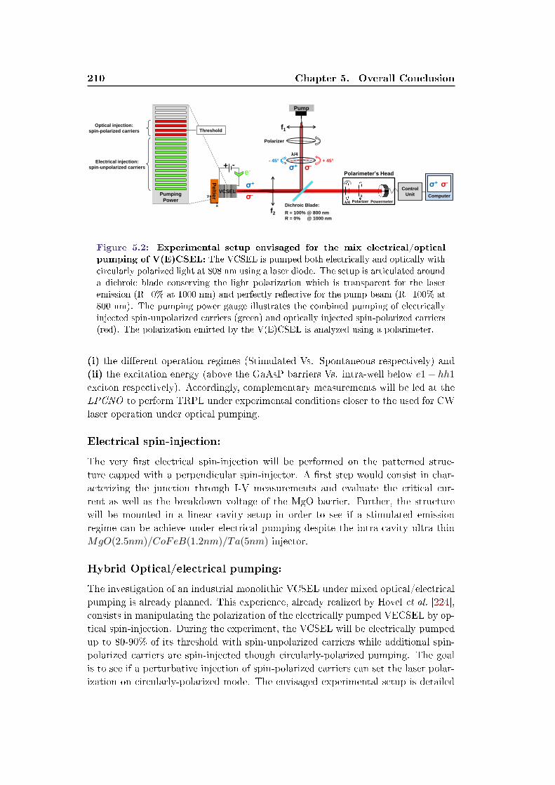
210 Chapter 5. Overall Conclusion
λ/4 Polarizer Powermeter
Computer
Control
Unit
σ+ σ-
Polarimeter’s Head
Peltie
r y
x
VCSEL
f2
f1
Pump
Polarizer
λ/4
+ 45° - 45°
σ- σ+
σ-
σ+
+ - e-
Dichroic Blade:
R = 100% @ 800 nm
R = 0% @ 1000 nm
Pumping
Power
Threshold Optical injection:
spin-polarized carriers
Electrical injection:
spin-unpolarized carriers
Figure 5.2: Experimental setup envisaged for the mix electrical/optical
pumping of V(E)CSEL: The VCSEL is pumped both electrically and optically with
circularly polarized light at 808 nm using a laser diode. The setup is articulated around
a dichroic blade conserving the light polarization which is transparent for the laser
emission (R=0% at 1000 nm) and perfectly reective for the pump beam (R=100% at
800 nm). The pumping power gauge illustrates the combined pumping of electrically
injected spin-unpolarized carriers (green) and optically injected spin-polarized carriers
(red). The polarization emitted by the V(E)CSEL is analyzed using a polarimeter.
(i) the dierent operation regimes (Stimulated Vs. Spontaneous respectively) and(ii) the excitation energy (above the GaAsP barriers Vs. intra-well below e1− hh1
exciton respectively). Accordingly, complementary measurements will be led at theLPCNO to perform TRPL under experimental conditions closer to the used for CWlaser operation under optical pumping.
Electrical spin-injection:
The very rst electrical spin-injection will be performed on the patterned struc-ture capped with a perpendicular spin-injector. A rst step would consist in char-acterizing the junction through I-V measurements and evaluate the critical cur-rent as well as the breakdown voltage of the MgO barrier. Further, the structurewill be mounted in a linear cavity setup in order to see if a stimulated emissionregime can be achieve under electrical pumping despite the intra-cavity ultra-thinMgO(2.5nm)/CoFeB(1.2nm)/Ta(5nm) injector.
Hybrid Optical/electrical pumping:
The investigation of an industrial monolithic VCSEL under mixed optical/electricalpumping is already planned. This experience, already realized by Hovel et al. [224],consists in manipulating the polarization of the electrically pumped VECSEL by op-tical spin-injection. During the experiment, the VCSEL will be electrically pumpedup to 80-90% of its threshold with spin-unpolarized carriers while additional spin-polarized carriers are spin-injected though circularly-polarized pumping. The goalis to see if a perturbative injection of spin-polarized carriers can set the laser polar-ization on circularly-polarized mode. The envisaged experimental setup is detailed

5.3. Perspectives, challenges and future applications 211
in gure 5.2. This experiment will stand as a preliminary examination to align andoptimize the experimental setup before performing the same experiment using ourVECSEL structures designed for electrical pumping.
Spin-information propagation over very long distances:
Finally, combined with the new research eld of all-optical magnetization switching,Spin-lasers could become the missing conceptual link toward an all-spintronics basedcircuit logic. Indeed, in the future, it could be envisage to transfer spin-informationover kilometric distances by propagating it in optical bers after encoding on thelight polarization.Magnetization reversal using circularly polarized light provides a way to controlmagnetization without any external magnetic eld and has the potential to revolu-tionize magnetic data storage [40, 359]. The low power manipulation of magnetiza-tion, preferably at ultra-short timescales, has become a fundamental challenge withimplications for future magnetic information memory and storage technologies. TheAll Optical-Helipticity Dependent Switching (AO-HDS) occurs through transfer ofangular momentum from incident circularly-polarized photons to a multilayer mag-netization. In short, it can be seen as the reverse mechanism to the one convertingspin-information into light polarization information in Spin-lasers. AO-HDS canbe observed not only in selected rare earth-transition metal (RE-TM) alloy lmsbut also in a much broader variety of materials, including RE-TM alloys, multi-layers and heterostructures. It has recently been demonstrate that (Co/Pt)×3 andRE-free Co-Ir-based synthetic ferrimagnetic heterostructures designed to mimic themagnetic properties of RE-TM alloys also exhibit AO-HDS [40]. The discovery ofAO-HDS in RE-free TM-based heterostructures can enable breakthroughs for nu-merous applications because it exploits materials that are used in magnetic datastorage, memories and logic technologies.
The communication process for the propagation of spin-information over verylong distances would break down into four essential steps (Figure 5.3):
1. Conversion of the magnetic bit information encode on an ultra-thin ferromag-netic layer into circularly-polarized light using an electrically spin-injectedVECSEL.
2. Fiber coupling of the VECSEL with an optical ber conserving the light po-larization information.
3. Propagation of the 100% σ+- or σ−-polarized light in the optical ber to-ward the terminal device (High density magnetic recording media, Magneticelectrode of a spin-transistor,. . .).
4. At the optical ber output, the preserved spin-information contained in thecircular-polarization is re-encoded onto a magnetic media through All-OpticalHelipticity Dependent Switching.
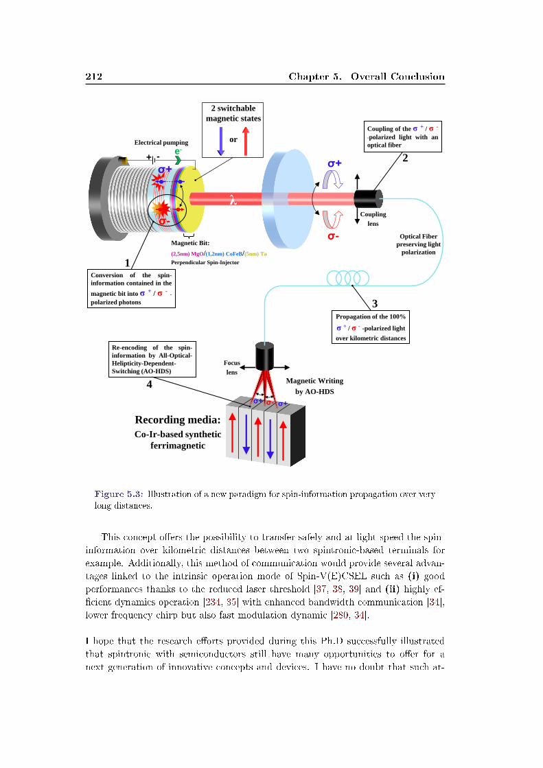
212 Chapter 5. Overall Conclusion
Recording media:
Co-Ir-based synthetic
ferrimagnetic
λ
+ - e-
σ+
σ- Magnetic Bit:
(2,5nm) MgO/(1,2nm) CoFeB/(5nm) Ta
Perpendicular Spin-Injector
Electrical pumping
2 switchable
magnetic states
or
Coupling
lens
σ+
σ-
1 Conversion of the spin-
information contained in the
magnetic bit into σ + / σ - -
polarized photons
2
Coupling of the σ + / σ - -polarized light with an
optical fiber
Optical Fiber
preserving light
polarization
σ+ σ-
Magnetic Writing
by AO-HDS
Focus
lens
σ+
3 Propagation of the 100%
σ + / σ - -polarized light
over kilometric distances
4
Re-encoding of the spin-
information by All-Optical-
Helipticity-Dependent-
Switching (AO-HDS)
Figure 5.3: Illustration of a new paradigm for spin-information propagation over very
long distances.
This concept oers the possibility to transfer safely and at light-speed the spin-information over kilometric distances between two spintronic-based terminals forexample. Additionally, this method of communication would provide several advan-tages linked to the intrinsic operation mode of Spin-V(E)CSEL such as (i) goodperformances thanks to the reduced laser threshold [37, 38, 39] and (ii) highly ef-cient dynamics operation [234, 35] with enhanced bandwidth communication [34],lower frequency chirp but also fast modulation dynamic [280, 34].
I hope that the research eorts provided during this Ph.D successfully illustratedthat spintronic with semiconductors still have many opportunities to oer for anext generation of innovative concepts and devices. I have no doubt that such at-

5.3. Perspectives, challenges and future applications 213
tractive beyond state-of-the-art applications will stimulate an important researcheort in a near future. To this day, ideas of innovative applications using Spin-Lasers are just emerging and such devices, borned from the fusion of Spintronicsand Semiconductor-Photonics, just revealed an innitesimal part of their capabili-ties.

Appendix A
Complementary calculation
related to spin-injection into
semiconductors
Contents
A.1 Formal demonstration of the General Boltzmann equation 215
A.2 Valet-Fert Model: Expressions of the electrochemical po-
tentials and the associated currents . . . . . . . . . . . . . . 218
A.3 Valet-Jarès Model: Expressions of the electrochemical
potentials and the associated currents . . . . . . . . . . . . . 219
A.1 Formal demonstration of the General Boltzmann
equation
The semi-classical treatment of the electronic transport starts by considering anelectron gas described as a wave packet Φ and dened in the direct space by theposition ~r. The application of an electric eld induces a shift of all carriers inthe phases space while at the same time the random collisions tend to bring backthe electrons toward their equilibrium distribution. Hence, the carriers distribu-tion function f(~k,~r, t) fully characterize the system evolution. It is dened so asf(~k, ~r, t)d~kd~r/(4π3) represents the number of electrons in the considered band con-tained in the innitesimal phase space element d~kd~r at time t. Here, we are going toidentify the nature of this function by studying the dynamical equilibrium betweenthe carriers acceleration in the electric eld and their diusion by the crystallinenetwork [360].
The localized Gaussian wave function representing the electron gas is dened by:
Φ~k =∑~k
u~k · exp
(i~k ·
[~r − 1
~dE(~k)
d~kt
])· exp
(− α[~k − ~k0]
)2 (A.1)

216Appendix A. Complementary calculation related to spin-injection into
semiconductors
where u~k is the base vector, E(~k) is the electric eld, ~k0 is the wave vectorcorresponding the rest system without any applied electric eld and α is a positiveinteger characterizing the shape of the wave packet envelope.
One must also take into account the carrier scattering probability by the crystallinenetwork W~k~k′
. The probability of an electron to scatter from an initial state Φ~k toa nal state ψ~k′ is given by Fermi golden rule:
W~k~k′=
2π
~∣∣⟨Ψ~k′
∣∣V (~r)∣∣Φ~k⟩∣∣2N(EF ) (A.2)
where V (~r) is the perturbation Hamiltonian materializing the applied electricpotential and N(EF ) is the nal Density Of State (DOS) at the Fermi level.
Thanks to the carrier scattering probability it is now possible to write the trans-port equation. The temporal evolution of the distribution function is equal to thecollision integral calculated by summing the scattering probabilities over k:
df
dt=∂f
∂t
∣∣∣∣scattering
⇐⇒ ∂f
∂t+∂f
∂~r· ∂~r∂t
∣∣∣∣diusion
+∂f
∂~k· ∂~k
∂t
∣∣∣∣∣drift
=∂f
∂t
∣∣∣∣scattering
(A.3)
where:
• The diusion term take into account the speed of the electronic wave packet~v(~k):
∂~r
∂t= ~v(~k) =
1
~dE(~k)
d~k(A.4)
• The drift component describes the global motion induced by the dierent in-system forces. In the approximation of the free electron gas the drifting force is
generated by the applied electromagnetic eld ~F = ~∂~k∂t = −e[~E + ~v(~k)× ~H
].
Hence:
∂f
∂~k· ∂~k
∂t
∣∣∣∣∣drift
= − e~
[~E + ~v(~k)× ~H
] ∂f∂~k
(A.5)

A.1. Formal demonstration of the General Boltzmann equation 217
• The scattering term represents the collision integral. Physically, it correspondsto the total rate at which the distribution function is changing due to collisions.We can notice that as the electrons can scatter into (W~k′~k
) or outo (W~k~k′)
the considered d~k element, the collision integral correspond to the sum of(∂f(~k)/∂t)in and (∂f(~k)/∂t)out. In the relaxation-time approximation, it canbe expressed as follow [360]:
∂f(~k)
∂t
∣∣∣∣∣scattering
= −f(~k)− f0(~k)
τ(~k)(A.6)
where f0(~k) is the non-perturbed Fermi-Dirac distribution function and τ(~k)
is the characteristic scattering time dene such as dt/τ(~k) is the probabilityfor an electron to experience a collision in the innitesimal time interval dt.
The equation (A.3) can then be rewritten by taking into account these develop-ments:
∂f
∂t+ ~v
∂f
∂~r− e
~
[~E + ~v × ~H
] ∂f∂~k
= −f − f0
τ(A.7)
This fundamental equation is the general Boltzmann equation describing theelectronic transport.
Comments:
I If quantum interferences become dominants it is necessary to add a quantumcorrection term in order to take into account the weak localization eects, theelectron-electron interactions, etc... [361].
I The previously developed Boltzmann model is valid for a diusive system.In case of a ballistic electrons regime, a formalism based on non-equilibriumGreen functions should be preferentially considered to study the electronictransport in a conductive system.
I Equation (A.7)stays valid under two conditions. Firstly, the wave packet widthin the phase space needs to be negligible compare to the 1st Brillouin-zone:∆~k a. Secondly, the electron mean free path must stay greater than the DeBroglie wavelength associated to the wave packet: λ > λΦ

218Appendix A. Complementary calculation related to spin-injection into
semiconductors
A.2 Valet-Fert Model: Expressions of the electrochemi-
cal potentials and the associated currents
For a F/N bilayer system, the general solutions of the electrochemical potentialsand the associated currents obtained from the Valet-Fert theory are given by:
For a ferromagnetic layer numerated (n) with "up" magnetization:
∆µ(n)F (z) = K
(n)F2 · exp
(z
lFsf
)+K
(n)F3 · exp
(− z
lFsf
)(A.8)
µ(n)F+ (z) = eρ∗F (1− β2)Jz +K
(n)1 + (1 + β)
[∆µ
(n)F
]µ
(n)F− (z) = eρ∗F (1− β2)Jz +K
(n)1 − (1− β)
[∆µ
(n)F
] (A.9)
J
(n)F+ (z) = (1− β)
J
2+
1
2erF
[K
(n)F2 · exp
(z
lFsf
)−K(n)F
3 · exp
(− z
lFsf
)]
J(n)F− (z) = (1 + β)
J
2− 1
2erF
[K
(n)F2 · exp
(z
lFsf
)−K(n)F
3 · exp
(− z
lFsf
)](A.10)
For a F layer with "down" magnetization, one has to interchange the positiveand negative index to get the related expressions.
In the same way, for a non-magnetic layer numerated (n+1):
∆µ(n+1)N (z) = K
(n+1)N2 · exp
(z
lNsf
)+K
(n+1)N3 · exp
(− z
lNsf
)(A.11)
µ(n+1)N+ (z) = eρ∗NJz +K
(n+1)1 +
[∆µ
(n+1)N
]µ
(n+1)N− (z) = eρ∗NJz +K
(n+1)1 −
[∆µ
(n+1)N
] (A.12)
J
(n+1)N+ (z) =
J
2+
1
2erF
[K
(n)N2 · exp
(z
lFsf
)−K(n)N
3 · exp
(− z
lFsf
)]
J(n+1)N− (z) =
J
2− 1
2erF
[K
(n)N2 · exp
(z
lFsf
)−K(n)N
3 · exp
(− z
lFsf
)] (A.13)
The integration constants K(n)Fi and K(n+1)N
i can be determined by taking intoaccount the boundary conditions (2.12) at each interfaces.

A.3. Valet-Jarès Model: Expressions of the electrochemical potentialsand the associated currents 219
A.3 Valet-Jarès Model: Expressions of the electrochem-
ical potentials and the associated currents
For a F/SC bilayer system, the general solutions of the electrochemical potentialsand the associated currents obtained from the Fert-Jarès theory are given by:
For the ferromagnetic layer with "up" magnetization:
∆µF (z) = KF2 · exp
(z
lFsf
)(A.14)
µF+(z) = eρ∗F (1− β2)Jz +K1 + (1 + β)KF
2 · exp
(z
lFsf
)
µF−(z) = eρ∗F (1− β2)Jz +K1 − (1− β)KF2 · exp
(z
lFsf
) (A.15)
JF+ (z) = (1− β)
J
2+
1
2erFKF
2 · exp
(z
lFsf
)
JF− (z) = (1 + β)J
2− 1
2erFKF
2 · exp
(z
lFsf
) (A.16)
For a F layer with "down" magnetization, one has to interchange the positiveand negative index to get the related expressions.
For the semiconductor:
∆µSC(z) = KSC3 · exp
(− z
lSCsf
)(A.17)
µSC+ (z) = eρ∗SCJz +K1 +KSC
3 · exp
(− z
lSCsf
)
µSC− (z) = eρ∗SCJz +K1 −KSC3 · exp
(− z
lSCsf
) (A.18)
JSC+ (z) =
J
2− 1
2erSCKSC
3 · exp
(− z
lSCsf
)
JSC− (z) =J
2+
1
2erSCKSC
3 · exp
(− z
lSCsf
) (A.19)

220Appendix A. Complementary calculation related to spin-injection into
semiconductors
Here again, the integration constants KFi and KSC
i can be determined using theboundary conditions (2.12).
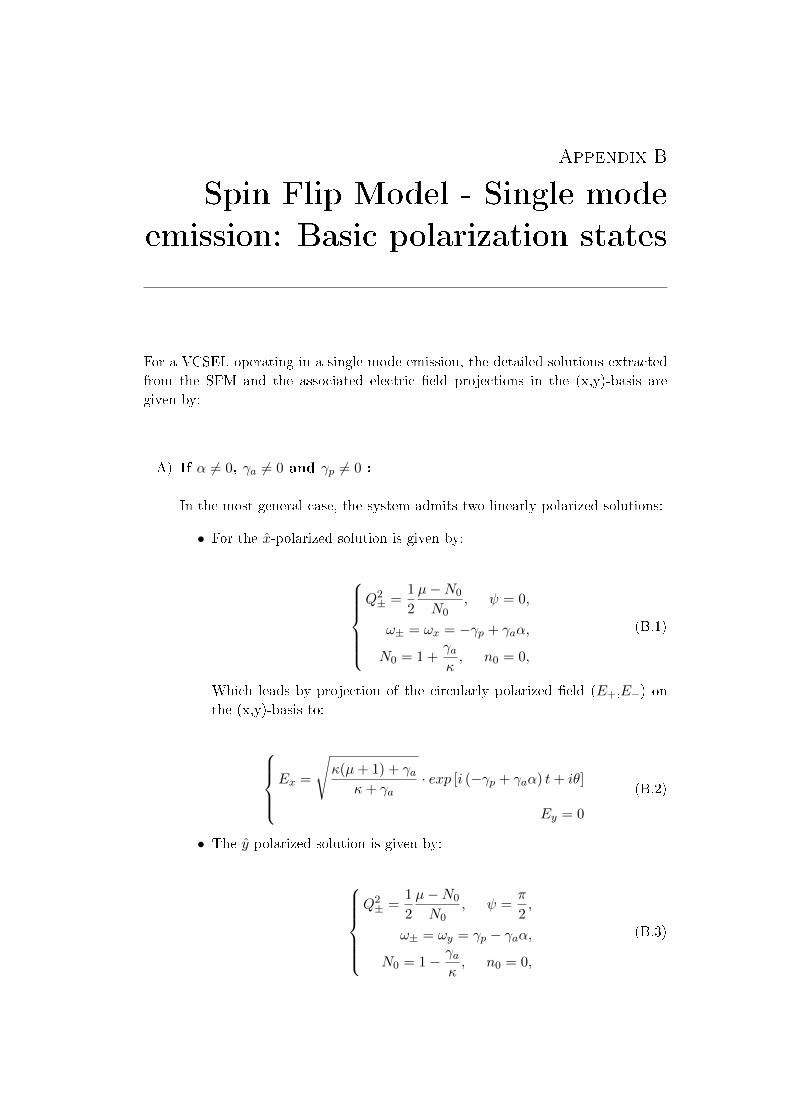
Appendix B
Spin Flip Model - Single mode
emission: Basic polarization states
For a VCSEL operating in a single mode emission, the detailed solutions extractedfrom the SFM and the associated electric eld projections in the (x,y)-basis aregiven by:
A) If α 6= 0, γa 6= 0 and γp 6= 0 :
In the most general case, the system admits two linearly polarized solutions:
• For the x-polarized solution is given by:
Q2± =
1
2
µ−N0
N0, ψ = 0,
ω± = ωx = −γp + γaα,
N0 = 1 +γaκ, n0 = 0,
(B.1)
Which leads by projection of the circularly polarized eld (E+,E−) onthe (x,y)-basis to:
Ex =
√κ(µ+ 1) + γa
κ+ γa· exp [i (−γp + γaα) t+ iθ]
Ey = 0
(B.2)
• The y-polarized solution is given by:
Q2± =
1
2
µ−N0
N0, ψ =
π
2,
ω± = ωy = γp − γaα,
N0 = 1− γaκ, n0 = 0,
(B.3)

222Appendix B. Spin Flip Model - Single mode emission: Basic
polarization states
Which leads by projection of the circularly polarized eld (E+,E−) onthe (x,y)-basis to:
Ex = 0
Ey =
√κ(µ+ 1) + γa
κ+ γa· exp [−i (−γp + γaα) t+ iθ]
(B.4)
B) If α 6= 0 and γa = γp = 0 :
If the VCSEL is perfectly isotropic the system admits a unique linearly polar-ized solution given by:
Q2± =
1
2(µ− 1), ψ 6= 0
ω± = 0,
N0 = 1, n0 = 0,
(B.5)
Which leads by projection of the linearly polarized eld (E+,E−) on the (x,y)-basis to:
Ex =
√µ− 1cosψ
Ey =√µ− 1sinψ
(B.6)
C) If α 6= 0, γa = 0 and γp 6= 0:
In this case the system admits two linearly- and two elliptically-polarizedsolution:
• The x-polarized solution (Figure 2.28 (a) 1©) is given by:
Q2± =
1
2(µ− 1), ψ = 0,
ω± = −γp,N0 = 1, n0 = 0,
(B.7)
Which leads in the (x,y)-basis to:
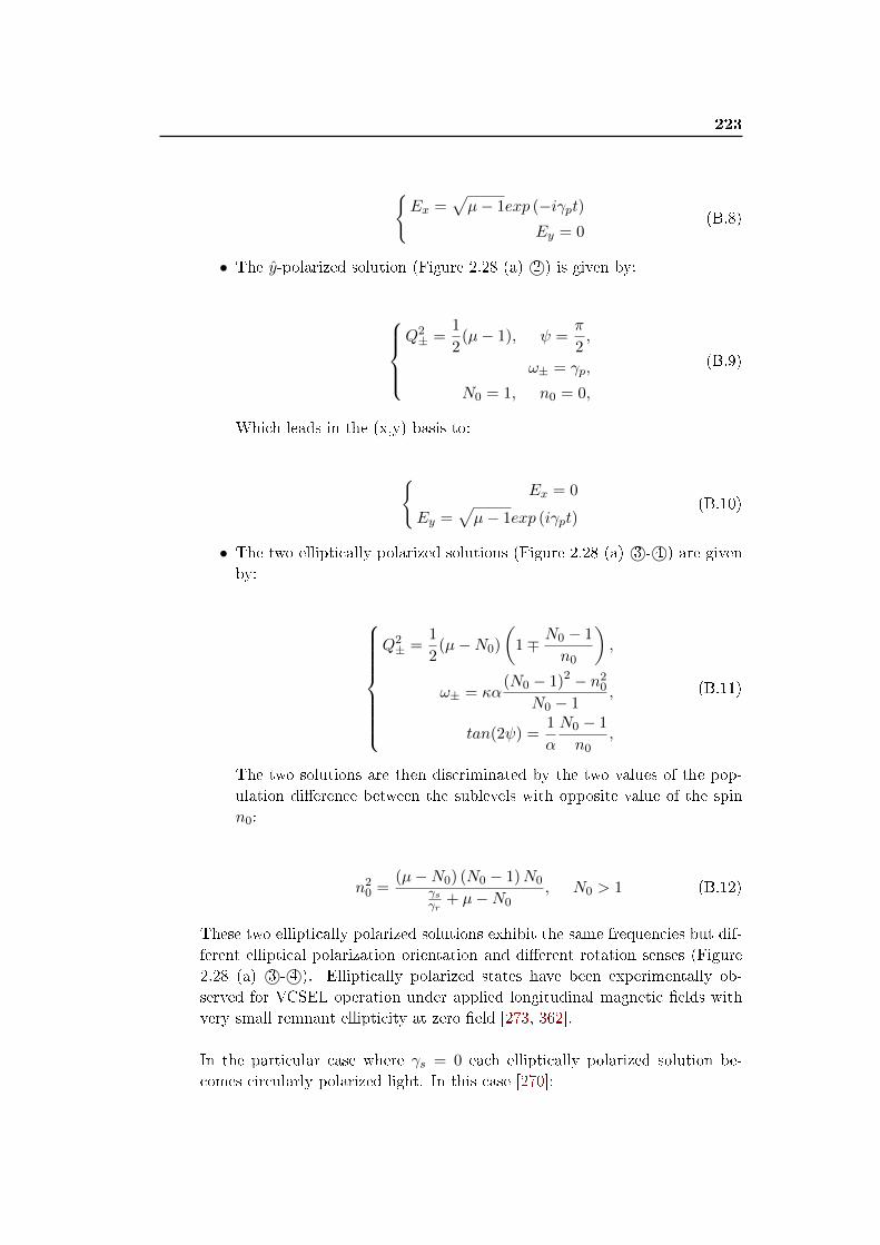
223
Ex =
√µ− 1exp (−iγpt)
Ey = 0(B.8)
• The y-polarized solution (Figure 2.28 (a) 2©) is given by:
Q2± =
1
2(µ− 1), ψ =
π
2,
ω± = γp,
N0 = 1, n0 = 0,
(B.9)
Which leads in the (x,y)-basis to:
Ex = 0
Ey =√µ− 1exp (iγpt)
(B.10)
• The two elliptically polarized solutions (Figure 2.28 (a) 3©- 4©) are givenby:
Q2± =
1
2(µ−N0)
(1∓ N0 − 1
n0
),
ω± = κα(N0 − 1)2 − n2
0
N0 − 1,
tan(2ψ) =1
α
N0 − 1
n0,
(B.11)
The two solutions are then discriminated by the two values of the pop-ulation dierence between the sublevels with opposite value of the spinn0:
n20 =
(µ−N0) (N0 − 1)N0γsγr
+ µ−N0, N0 > 1 (B.12)
These two elliptically polarized solutions exhibit the same frequencies but dif-ferent elliptical polarization orientation and dierent rotation senses (Figure2.28 (a) 3©- 4©). Elliptically polarized states have been experimentally ob-served for VCSEL operation under applied longitudinal magnetic elds withvery small remnant ellipticity at zero eld [273, 362].
In the particular case where γs = 0 each elliptically polarized solution be-comes circularly polarized light. In this case [270]:

224Appendix B. Spin Flip Model - Single mode emission: Basic
polarization states
N0 =µ+ γs
γr
1 + γsγr
, n0 = ±(N0 − 1) (B.13)
where n0 > 0 and n0 < 0 correspond the left and right circularly polarizedmodes respectively. Nevertheless, these circularly polarized states are neverfound to be stable solutions of (3.63)-(3.65) [236]. These situation correspondsto the previous case B) where for a perfectly isotropic VCSEL (γa = γp = 0)linearly polarized states exist with an arbitrary orientation . Birefringencealone (γp) is able to x the direction of polarization selecting two preferredvalues of ψ which can be identied with the x and y linearly polarized states.
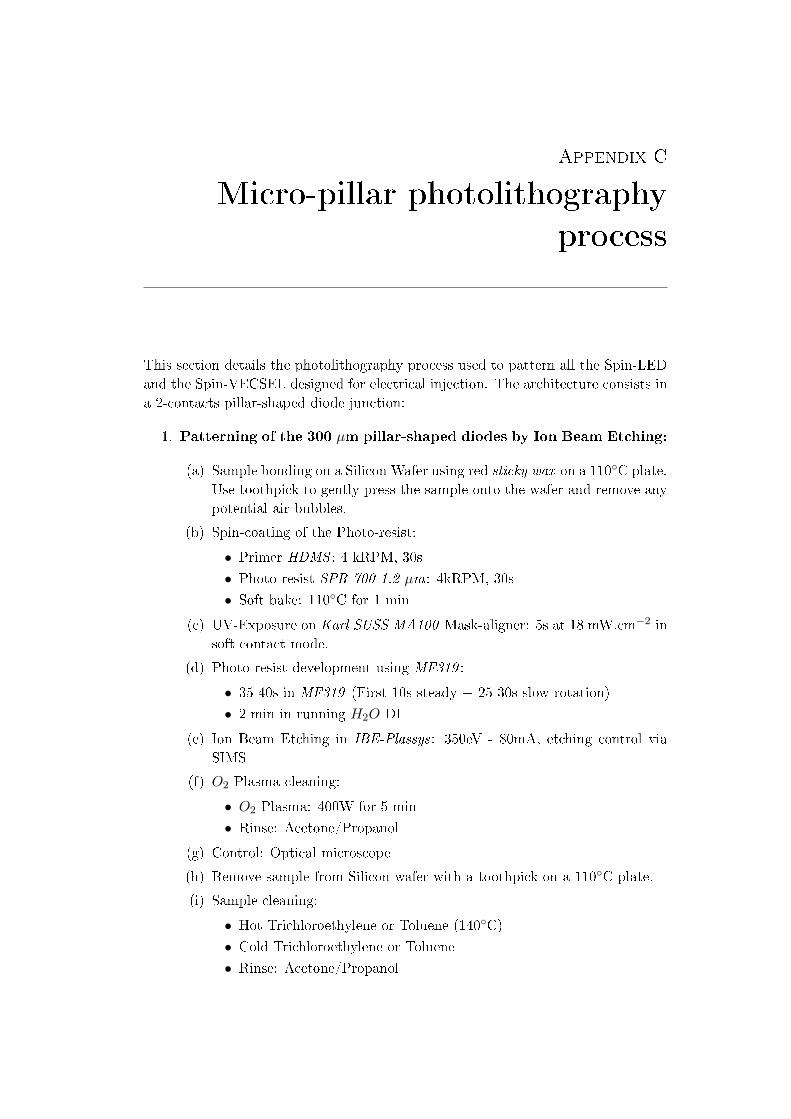
Appendix C
Micro-pillar photolithography
process
This section details the photolithography process used to pattern all the Spin-LEDand the Spin-VECSEL designed for electrical injection. The architecture consists ina 2-contacts pillar-shaped diode junction:
1. Patterning of the 300 µm pillar-shaped diodes by Ion Beam Etching:
(a) Sample bonding on a Silicon Wafer using red sticky wax on a 110C plate.Use toothpick to gently press the sample onto the wafer and remove anypotential air bubbles.
(b) Spin-coating of the Photo-resist:
• Primer HDMS : 4 kRPM, 30s
• Photo-resist SPR 700 1.2 µm: 4kRPM, 30s
• Soft bake: 110C for 1 min
(c) UV-Exposure on Karl SUSS MA100 Mask-aligner: 5s at 18 mW.cm−2 insoft contact mode.
(d) Photo-resist development using MF319 :
• 35-40s in MF319 (First 10s steady + 25-30s slow rotation)
• 2 min in running H2O DI
(e) Ion Beam Etching in IBE-Plassys: 350eV - 80mA, etching control viaSIMS
(f) O2-Plasma cleaning:
• O2-Plasma: 400W for 5 min
• Rinse: Acetone/Propanol
(g) Control: Optical microscope
(h) Remove sample from Silicon wafer with a toothpick on a 110C plate.
(i) Sample cleaning:
• Hot Trichloroethylene or Toluene (140C)
• Cold Trichloroethylene or Toluene
• Rinse: Acetone/Propanol

226 Appendix C. Micro-pillar photolithography process
2. 110 µm top and bottom contact deposition by Lift-O:
(a) Sample bonding on a Silicon Wafer using Crystalbond 555 on a 60Cplate. Use toothpick to gently press the sample onto the wafer and removeany potential air bubbles.
(b) Spin-coating of the Photo-resist:
• Primer HDMS : 4 kRPM, 30s
• Photo-resist SPR 700 1.2 µm: 4kRPM, 30s
• Soft bake: 110C for 1 min
(c) Remove sample from Silicon wafer with a toothpick on a 60C plate andrinse 2 min in running H2O DI
(d) Photo-resist hardening:
• Chlorobenzene for 10 min
• Dry with N2
• Hard bake: 110C for 1 min
(e) Sample bonding on a Silicon Wafer using red sticky wax on a 110C plate.Use toothpick to gently press the sample onto the wafer and remove anypotential air bubbles.
(f) UV-Exposure on Karl SUSS MA100 Mask-aligner: 10s at 18 mW.cm−2
in soft contact mode.
(g) Photo-resist development using MF319 :
• 1min30s in MF319 (First 10s steady + 1min20s slow rotation every20s)
• 2 min in running H2O DI
(h) Metallic contacts deposition (Ask the Thales technological platform):
• Plasma Etching: 200V â 110mA for 1 min
• (50nm) Ti / (250nm) Au by side evaporation
(i) Lift-O:
• Minimum 1H in Acetone
• Acetone gun 7→ LIFT
• Rinse: Spray Acetone/Propanol
(j) Control: Optical microscope
(k) Remove sample from Silicon wafer with a toothpick on a 110C plate.
(l) Sample cleaning:
• Hot Trichloroethylene or Toluene (140C)
• Cold Trichloroethylene or Toluene
• Rinse: Acetone/Propanol

Appendix D
Formal demonstration of the
relation between frequency
detuning and birefringence
In this appendix, we aim at giving the relationship between the frequency detuningbetween the TE- and TM-modes emitted by a laser and the intrinsic birefringence of1/2-VCSEL. We choose for notation conventions to identify the frequency in the op-tical domain as ν and the frequency in the electrical domain as f . We consider thegeneral case of a VECSEL emitting on the TE-mode linearly-polarized along theextraordinary-axis while the spontaneous emission of TM-mode linearly-polarizedalong the ordinary-axis is amplied by the cavity but still below threshold (FigureD.1 (a)).
We dene L as the cavity length, c the celerity of light, l the thickness of theactive medium while ne and no are the refractive indexes seen in the 1/2-VCSEL bythe extraordinary and ordinary polarizations respectively. Accordingly, the opticalfrequencies associated with the extraordinary and ordinary polarization modes atthe order p and q are respectively given by:
νpTE = p · c
2 [L+ (ne − 1)l]
νqTM = q · c
2 [L+ (no − 1)l]
(D.1)
However, as the birefringence is expected to be relatively small, the order p andq are equals. Hence, the system of equations becomes:
νpTE = p · c
2 [L+ (ne − 1)l]
νpTM = p · c
2 [L+ (no − 1)l]
(D.2)
After projection of the two ordinary and extraordinary optical spectra on thesame polarization axis (Figure D.1 (b)), we focus on the associated RF spectrum(Figure D.1 (c)). In the electrical domain, the corresponding spectrum displays

228Appendix D. Formal demonstration of the relation between frequency
detuning and birefringence
Optical spectrum (Raw emission)
Oscillating mode
Optical
Frequency (ν)
TM
TE
TM
TE
TM
TE
order p-1
order p
order p+1
Δν
νTEp
νTMp
νTEp+1
νTMp+1
νTEp-1
νTMp-1
Δν
(a) Optical spectrum (After projection on the same optical axis)
TE
Optical
Frequency (ν)
TM TM TE TM
TE order p-1
order p
order p+1
Δν Δν
FSR
νTEp
νTMp
νTEp+1
νTMp+1
νTEp-1
νTMp-1
(b) RF spectrum
(Electrical domain)
Electrical
Frequency (f)
0
f1 = νTEp – νTE
p-1
f2 = νTEp – νTM
p-1 f3 = νTMp+1 - νTE
p
(c)
Δf
FSR
Figure D.1: Optical and electrical mode spectra: (a) Optical spectrum emitted by the
laser. For a given mode, the frequency detuning between two adjacent orders is equal to
the Free Spectral Range (FSR) of the cavity. (b) Corresponding optical spectrum after
projection on the same polarization axis using a polarizer. (c) Associated electrical
spetrum after quadratic detection by a photodiode of the projected optical spectrum
at 45.
beating frequencies between the dierent optical modes. On gure D.1 (c): (i) thecentral peak (light blue) corresponds to the beating frequency f1 between the lasingTE-mode at the order p (optical frequency νpTE) and the Amplied SpontaneousEmission (ASE) of the TE-mode at the order p+1 (optical frequency νp+1
TE ). (ii) Onthe other hand, the satellite peak f2 (purple) corresponds to the beating frequencybetween the lasing TE-mode at the order p (optical frequency νpTE) and the ASE ofthe TM-mode at the order p-1 (optical frequency νp−1
TM ). Similarly, the satellite peakf3 (purple) corresponds to the beating frequencies between the lasing TE-mode atthe order p (optical frequency νpTE) and the ASE of the TM-mode at the order p+1(optical frequency νp+1
TM ). Obviously, the beating between the lasing TE-mode andthe nonlasing TM-modes at the order p is also present in the low frequency part ofthe spectrum. However, we do not rely on this peak for our measurements becauseit suers from pump to laser noise transfer as well as from CPO eects that cannotbe neglected for beatnotes below 1 GHz. The above dierent frequencies read:
f1 = νpTE − νp−1TE =
c
2Le
f2 = νpTE − νp−1TM =
pc
2
(1
Le− 1
Lo
)+
c
2Lo
f3 = νp+1TM − ν
pTE =
pc
2
(1
Lo− 1
Le
)+
c
2Le
(D.3)
where Le = L + (ne − 1)l and Lo = L + (no − 1)l are the optical lengths seenby the modes polarized along the extraordinary (TE) and the ordinary (TM) axisrespectively. Using (D.3), we further calculate the frequency detunings f1 − f2 and

229
f3− f1 between the central peak (f1) and the left (f2) and right (f3) satellite peaksrespectively (Figure D.1 (c)):
f1 − f2 =
c
2(1− p)
(1
Le− 1
Lo
)f3 − f1 =
c
2(1 + p)
(1
Lo− 1
Le
) (D.4)
Finally, the birefringence ∆n = ne − no can be extracted from (D.4):
∆f =(f1 − f2) + (f3 − f1)
2=
pc
2Lo
l∆n
Le= νo
l∆n
Le(D.5)
Then the dephasing ∆ϕ associated with the birefringence ∆n can be expressedfor a round-trip as:
∆ϕ =2π
λ2l∆n (D.6)
Finally, the expression (D.6) can be rewritten as follow using the relation ofequation (D.5):
∆ϕ
2π=
γ′
2π=
2L
c∆f (D.7)
where L ≈ Le ≈ Lo. This relation is established for a round-trip in the cavity.


Appendix E
Complementary information on
TRPL measurements
E.1 Experimental setup
Cryostat
Sample
mounted on
cold finger
10 K
λ/4
+ 45° - 45° σ- σ+
Polarizer
M
Photodiode
Ti:
Sa
Analizer
+ 45°
- 45°
λ/4
f1 f2
Spectrometer
Str
eak
Cam
era
Computer
0 500 1000 1500 20000.01
0.1
1 T = 10 K
No
rma
lize
d P
L i
nte
ns
ity
Delay (ps)
exc
=780nm ; P=1W ; = 410±5ps
exc
=780nm ; P=100W ; = 550±5ps
exc
=880nm ; P=100W ; = 680±5ps
exc
=900nm ; P=100W ; =670±5ps
• Laser Pulse: 1.5 ps
• Repetition rate: 80 MHz
• Temporal Resolution: ≈ 15 ps
• Temperature range: 10 – 300 K
Figure E.1: Schematic of the experimental setup used to performed the Time Re-
solved Photo-Luminescence measurements on Spin-LED and Spin-VECSEL.

232 Appendix E. Complementary information on TRPL measurements
E.2 Band-to-band transitions and excitation energies of
the InGaAs/GaAsP 12-VCSEL
Temperature Transition Energy (eV) Wavelength λ (nm)
300 K e1 − hh1 1.261 982.9
e2 − hh2 1.378 899
e1 − lh1 1.345 921.5
Gap In20%Ga80%As 1.214 1021
Gap GaAs 1.423 871
Gap GaAs95%P5% 1.463 847
10 K e1 − hh1 1.357 913
e2 − hh2 1.474 841
e1 − lh1 1.441 860
Gap In20%Ga80%As 1.310 946
Gap GaAs 1.519 816
Gap GaAs95%P5% 1.559 795
Table E.1: Band-to-band transition energies derived from k.p simulations of
In20%Ga80%As/GaAs95%P5% QW used as the active medium of the GaAs615 VES-
CEL. From 300 K to 10 K the energy gap shift of In20%Ga80%As and GaAs95%P5% has
been estimated to be approximately the same than the shift of the GaAs's gap: 95.9
meV.
Temperature Excitation Corresponding Comments
Wavelength (nm) Energy (eV)
300 K 769 1.612 Above GaAs and GaAsP
808 1.534 Above GaAs and GaAsP
845 1.466 Above GaAs and GaAsP
879 1.410 Under GaAs and GaAsP but above
e1 − hh1, e2 − hh2 and e1 − lh1
10 K 769 1.612 Above GaAs and GaAsP
845 1.466 Under GaAs and GaAsP but above
e1 − hh1, e2 − hh2 and e1 − lh1
Table E.2: Excitation energies of the Ti:Sa laser used to perform the TRPL measure-
ments at both low and room temperature.

E.3. Complementary TRPL measurements of the InGaAs/GaAsPGaAs615 1
2-VCSEL 233
E.3 Complementary TRPL measurements of the InGaAs/GaAsP
GaAs615 12-VCSEL
0 400 800 1200 1600 20000.01
0.1
1
T = 10 K
No
rma
lize
d P
L i
nte
ns
ity
Delay (ps)
10 mW ; = 900±6 ps
3 mW ; = 875±5 ps
1 mW ; = 690±5 ps
0,3 mW ; = 685±5 ps
Resonant Linear excitation
exc
= 870nm
Figure E.2: Carrier lifetime measurements at T=10 K for a resonant (870 nm) and
linearly-polarized pumping under variable excitation power ranging from 0.3 mW to
10 mW.
0 200 400 600 800 1000 1200 1400 1600-10
-5
0
5
10
15
20
Non-resonant Circular Excitation, exc
= 780nm:
Pexc
= 1 W ; s = 170±10 ps
Pexc
= 100 W ; s = 105±5 ps
Do
CP
(%
)
Delay (ps)
Figure E.3: Time Resolved Spin lifetime measurements: Comparison of Spin
lifetime measurements at T=10 K under non-resonant pumping at 780 nm for two
excitation power of 1 µW and 100 µW.


Appendix F
List of Publications
• "Accurate measurement of the residual birefringence in VECSEL:
Towards understanding of the polarization behavior under spin-
polarized pumping"
J. Frougier, G. Baili, I. Sagnes, D. Dol, J. M. George and M. AlouiniOptics Express Submitted (2014)
• "Large and robust electrical spin injection into GaAs at zero mag-
netic eld using an ultrathin CoFeB/MgO injector"
S. Liang, T. Zhang, P. Barate, J. Frougier, M. Vidal, P. Renucci, B. Xu, H.Jares, J. M. George, X. Devaux, M. Hehn, X. Marie, S. Mangin, H. Yang, A.Hallal, M. Chshiev, T. Amand, H. Liu, D. Liu, X. Han, Z. Wang and Y. LuPhysical Review B 90, 085390 (2014)
• "Electrical spin injection into InGaAs/GaAs quantum wells: A com-
parison between MgO tunnel barriers grown by sputtering and molec-
ular beam epitaxy methods"
P. Barate, S. Liang, T. T. Zhang, J. Frougier, M. Vidal, P. Renucci, X.Devaux, B. Xu, H. Jares, J. M. George, X. Marie, M. Hehn, S. Mangin, Y.Zhen, T. Amand, B. Tao, X. Han, Z. Wang and Y. LuApplied Physics Letters 105, 012404 (2014)
• "Control of light polarization using optically spin-injected vertical
external cavity surface emitting lasers"
J. Frougier, G. Baili, M. Alouini, I. Sagnes, H. Jares, A. Garnache, C.Deranlot, D. Dol and J. M. GeorgeApplied Physics Letters 103, 252402 (2013)
• "Spin Injection at Remanence into III-V Spin Light Emitting Diodes
using (Co/Pt) Ferromagnetic Injectors"
J. Zarpellon, H. Jares, J. Frougier, C. Deranlot, J. M. George, D. H. Mosca,A. Lemaitre, F. Freimuth, Quang Ha Duong, P. Renucci and X. MariePhysical Review B 86, 205314 (2012)


Appendix G
List of Conferences
• Invited Speaker:
08/17/2014: "Control of light polarization using spin-injected
opto-electronic devices with vertical geometries"
J. Frougier, T. T. Zhang, S. Liang, P. Barate, P. Renucci, X. Marie, G.Baili, M. Alouini, I. Sagnes, A. Garnache, H. Jares, Y. Lu and J. M.GeorgeSPIE-Spintronics VII, San Diego, USA
10/18/2012: "Towards Control of Light Polarization using elec-
tron spin in Half-VCSEL"
J. Frougier, G. Baili, M. Alouini, I. Sagnes, H. Jares, A. Garnache, D.Dol and J. M. GeorgeFirst VeCSEL Workshop, Montpellier, FRANCE
• Oral Communications:
11/04/2013: "Electrical Spin-Injection enhancement in III-V Spin-
LEDs: Towards control of light polarization using spin-injected
Lasers"
J. Frougier, T. T. Zhang, S. Liang, P. Barate, P. Renucci, X. Marie, G.Baili, M. Alouini, I. Sagnes, A. Garnache, H. Jares, Y. Lu and J. M.GeorgeMMM Conference, Denver, USA
10/15/2013: "Control of light polarization using spin-injected
VECSELs"
J. Frougier, G. Baili, M. Alouini, I. Sagnes, H. Jares, A. Garnache, D.Dol and J. M. GeorgeSecond VeCSEL Workshop, Montpellier, FRANCE

238 Appendix G. List of Conferences
• Seminars:
15/01/2015: "Towards Spin-LED and Spin-VECSEL operation at
magnetic remanence"
J. Frougier, G. Baili, M. Alouini, I. Sagnes, H. Jares, A. Garnache, D.Dol and J. M. GeorgeInstitut National des Sciences Appliquées, Toulouse, FRANCE
09/01/2015: "Towards Spin-LED and Spin-VECSEL operation at
magnetic remanence"
J. Frougier, G. Baili, M. Alouini, I. Sagnes, H. Jares, A. Garnache, D.Dol and J. M. GeorgeUniversity of Alabama at Birmingham, Birmingham, Alabama, USA
05/01/2015: "Towards Spin-LED and Spin-VECSEL operation at
magnetic remanence"
J. Frougier, G. Baili, M. Alouini, I. Sagnes, H. Jares, A. Garnache, D.Dol and J. M. GeorgeThe Pennsylvania State University, State College, Pennsylvania, USA
02/21/2013: "Towards Control of Light Polarization using elec-
tron spin in Half-VCSELs"
J. Frougier, G. Baili, M. Alouini, I. Sagnes, H. Jares, A. Garnache, D.Dol and J. M. GeorgeInstitut d'Électronique Fondamentale, Montpellier, FRANCE
01/17/2013: "Towards Control of Light Polarization using elec-
tron spin in Half-VCSELs"
J. Frougier, G. Baili, M. Alouini, I. Sagnes, H. Jares, A. Garnache, D.Dol and J. M. GeorgeUnité Mixte de Physique CNRS-Thales, Palaiseau, FRANCE
• Poster Communications:
07/29/2013: "Towards control of light polarization using spin-
injected VECSELs"
J. Frougier, G. Baili, M. Alouini, I. Sagnes, H. Jares, A. Garnache, D.Dol and J. M. GeorgeSpintech VII, Chicago, USA
03/19/2013: "Contrôle de la Polarisation Lumineuse d'un LASERpar injection de porteurs polarisées en spin"
J. Frougier, G. Baili, M. Alouini, I. Sagnes, H. Jares, A. Garnache, D.Dol and J. M. GeorgeXV Colloque Louis Néel, Tours, FRANCE

Bibliography
[1] M. N. Baibich et al., Physical Review Letters 61, 2472 (1988). (Cited onpages 1 and 11.)
[2] G. Binasch, P. Grunberg, F. Saurenbach, and W. Zinn, Physical Review B39, 4828 (1989). (Cited on pages 1 and 11.)
[3] M. Julliere, Physics Letters A 54, 225 (1975). (Cited on pages 1 and 11.)
[4] J. S. Moodera, L. R. Kinder, T. M. Wong, and R. Meservey, Physical ReviewLetters 74, 3273 (1995). (Cited on pages 1 and 11.)
[5] S. Yuasa, A. Fukushima, H. Kubota, Y. Suzuki, and K. Ando, Applied PhysicsLetters 89, 042505 (2006). (Cited on page 1.)
[6] W. H. Rippard, M. R. Pufall, S. Kaka, S. E. Russek, and T. J. Silva, PhysicalReview Letters 92, 027201 (2004). (Cited on page 1.)
[7] T. Yang, T. Kimura, and Y. Otani, Nature Physics 4, 851 (2008). (Cited onpages 1 and 38.)
[8] X. Lou et al., Nature Physics 3, 197 (2007). (Cited on pages 1, 38 and 198.)
[9] B. Dlubak et al., Nature Physics 8, 557 (2012). (Cited on pages 1 and 22.)
[10] M. H. D. Guimaraes et al., Nano Letters 12, 3512 (2012). (Cited on page 1.)
[11] L. E. Hueso et al., Nature 445, 410 (2007). (Cited on pages 1 and 22.)
[12] Z. H. Xiong, D. Wu, Z. Valy Vardeny, and J. Shi, Nature 427, 821 (2004).(Cited on page 1.)
[13] T. S. Santos et al., Physical Review Letters 98, 016601 (2007). (Cited onpage 1.)
[14] C. Barraud et al., Nature Physics 6, 615 (2010). (Cited on page 1.)
[15] S. A. Wolf, Science 294, 1488 (2001). (Cited on pages 1, 2 and 3.)
[16] J. F. Gregg, Nature Materials 6, 798 (2007). (Cited on page 2.)
[17] S. Datta and B. Das, Applied Physics Letters 56, 665 (1990). (Cited onpage 2.)
[18] J. C. R. Sanchez et al., Nature Communications 4 (2013). (Cited on page 2.)
[19] C. M. Jaworski et al., Nature Materials 9, 898 (2010). (Cited on pages 2and 40.)

240 Bibliography
[20] K. C. Hall and M. E. Flatte, Applied Physics Letters 88, 162503 (2006).(Cited on page 2.)
[21] S. Murakami, N. Nagaosa, and S.-C. Zhang, Science 301, 1348 (2003), PMID:12907808. (Cited on page 2.)
[22] B. T. Jonker, G. Kioseoglou, A. T. Hanbicki, C. H. Li, and P. E. Thompson,Nature Physics 3, 542 (2007). (Cited on pages 3 and 98.)
[23] O. M. J. van't Erve et al., Applied Physics Letters 91, 212109 (2007). (Citedon page 3.)
[24] L. Grenet et al., Applied Physics Letters 94, 032502 (2009). (Cited on pages 3,112 and 129.)
[25] S. P. Dash, S. Sharma, R. S. Patel, M. P. de Jong, and R. Jansen, Nature462, 491 (2009). (Cited on pages 3 and 38.)
[26] C. H. Li et al., Applied Physics Letters 91, 262504 (2007). (Cited on page 3.)
[27] C. H. Li, O. M. J. van't Erve, and B. T. Jonker, Nature Communications 2,245 (2011). (Cited on page 3.)
[28] Tomoyasu Taniyama, Eiji Wada, Mitsuru Itoh, and Masahito Yamaguchi,NPG Asia Materials 3, 65 (2011). (Cited on page 3.)
[29] R. Fiederling et al., Nature 402, 787 (1999). (Cited on pages 4, 53, 66, 67, 68and 97.)
[30] S. A. Crooker, D. D. Awschalom, J. J. Baumberg, F. Flack, and N. Samarth,Physical Review B 56, 7574 (1997). (Cited on pages 4 and 58.)
[31] H. Dery, Y. Song, P. Li, and I. Zutic, Applied Physics Letters 99, 082502(2011). (Cited on pages 4, 93 and 208.)
[32] D. Miller, Proceedings of the IEEE 97, 1166 (2009). (Cited on pages 4, 93and 208.)
[33] B. Ciftcioglu et al., Optics Express 20, 4331 (2012). (Cited on pages 4, 93and 208.)
[34] J. Lee, W. Falls, R. Oszwaldowski, and I. Zutic, Applied Physics Letters 97,041116 (2010). (Cited on pages 4, 72, 75, 76, 93, 208 and 212.)
[35] N. C. Gerhardt et al., Applied Physics Letters 99, 151107 (2011). (Cited onpages 4, 76, 93, 208 and 212.)
[36] H. Ando, T. Sogawa, and H. Gotoh, Applied Physics Letters 73, 566 (1998).(Cited on pages 4, 93, 94, 149, 174, 206 and 208.)

Bibliography 241
[37] M. Holub, J. Shin, D. Saha, and P. Bhattacharya, Physical Review Letters98, 146603 (2007). (Cited on pages 4, 75, 76, 93, 96, 136, 149, 174, 196, 206,208 and 212.)
[38] J. Rudolph, S. Dohrmann, D. Hagele, M. Oestreich, and W. Stolz, AppliedPhysics Letters 87, 241117 (2005). (Cited on pages 4, 76, 77, 93, 94, 208and 212.)
[39] C. Gothgen, R. Oszwaldowski, A. Petrou, and I. Zutic, Applied Physics Letters93, 042513 (2008). (Cited on pages 4, 72, 75, 76, 77, 93, 208 and 212.)
[40] S. Mangin et al., Nature Materials 13, 286 (2014). (Cited on pages 4, 93, 204,208 and 211.)
[41] N. Gerhardt et al., Electronics Letters 42, 88 (2006). (Cited on pages 4, 94,95, 174 and 206.)
[42] S. Iba, S. Koh, K. Ikeda, and H. Kawaguchi, Applied Physics Letters 98,081113 (2011). (Cited on pages 4, 94, 95, 153, 173, 174 and 206.)
[43] K. Schires et al., Optics Express 20, 3550 (2012). (Cited on pages 4, 94, 149,174 and 206.)
[44] D. Basu, D. Saha, and P. Bhattacharya, Physical Review Letters 102, 093904(2009). (Cited on pages 4, 76, 95 and 96.)
[45] J. Sinova and I. Zutic, Nature Materials 11, 368 (2012). (Cited on page 5.)
[46] S. Hoogland et al., IEEE Photonics Technology Letters 12, 1135 (2000).(Cited on pages 6, 137, 139 and 141.)
[47] D. Lorenser et al., IEEE Journal of Quantum Electronics 42, 838 (2006).(Cited on pages 6 and 141.)
[48] R. Haring et al., IEEE Journal of Quantum Electronics 38, 1268 (2002).(Cited on pages 6 and 141.)
[49] A. Garnache et al., Applied Physics Letters 80, 3892 (2002). (Cited on pages 6and 141.)
[50] P. Klopp, F. Saas, M. Zorn, M. Weyers, and U. Griebner, Optics Express 16,5770 (2008). (Cited on pages 6 and 141.)
[51] D. Maas et al., Applied Physics B 88, 493 (2007). (Cited on pages 6 and 141.)
[52] F. Camargo et al., Two-cross-polarized-frequency VECSEL at 852nm for CPT-based cs clocks, in Advanced Solid-State Lasers Congress, edited by G. Huberand Moulton, OSA Technical Digest (online), page JTh2A.20, Optical Societyof America, 2013. (Cited on pages 6 and 142.)

242 Bibliography
[53] T. E. Darcie, A. Stohr, and P. K. L. Yu, Lightwave Technology, Journal of26, 2336 (2008). (Cited on pages 6 and 142.)
[54] N. F. Mott, Proceedings of the Royal Society of London. Series A - Mathe-matical and Physical Sciences 153, 699 (1936). (Cited on page 11.)
[55] N. F. Mott, Proceedings of the Royal Society of London. Series A - Mathe-matical and Physical Sciences 156, 368 (1936). (Cited on page 11.)
[56] A. Fert and I. A. Campbell, Physical Review Letters 21, 1190 (1968). (Citedon page 11.)
[57] C. Chappert, A. Fert, and F. N. Van Dau, Nature Materials 6, 813 (2007).(Cited on pages 12, 16 and 21.)
[58] A. G. Aronov and G. E. Pikus, Sov. Phys. Semicond. 10, 698 (1976). (Citedon pages 11 and 17.)
[59] M. Johnson and R. H. Silsbee, Physical Review Letters 55, 1790 (1985).(Cited on page 11.)
[60] B. Dieny et al., Physical Review B 43, 1297 (1991). (Cited on page 12.)
[61] Forbes, Declining growth projections for hard disk drive industry in 2013,2014. (Cited on page 12.)
[62] T. Valet and A. Fert, Physical Review B 48, 7099 (1993). (Cited on pages 13,17, 18 and 19.)
[63] A. Fert and H. Jares, Physical Review B 64, 184420 (2001). (Cited onpages 13, 20, 21, 98, 112 and 198.)
[64] P. C. van Son, H. van Kempen, and P. Wyder, Physical Review Letters 58,2271 (1987). (Cited on pages 14 and 18.)
[65] M. Johnson and R. H. Silsbee, Physical Review Letters 60, 377 (1988). (Citedon pages 14 and 18.)
[66] R. Magno and J. H. Pifer, Physical Review B 10, 3727 (1974). (Cited onpage 17.)
[67] J. Peiro, Phénomène d'injection et de décohérence de spin dans des struc-tures semiconductrices, PhD thesis, Unité-Mixte de Physique CNRS-Thales -Université Parsi-Sud, 2012. (Cited on pages 20, 28, 51 and 53.)
[68] Z. G. Yu and M. E. Flatté, Physical Review B 66, 201202 (2002). (Cited onpage 21.)
[69] A. M. Bratkovsky and V. V. Osipov, Journal of Applied Physics 96, 4525(2004). (Cited on page 21.)

Bibliography 243
[70] W. Y. Lee et al., Journal of Applied Physics 85, 6682 (1999). (Cited onpage 21.)
[71] P. R. Hammar, B. R. Bennett, M. J. Yang, and M. Johnson, Physical ReviewLetters 83, 203 (1999). (Cited on page 21.)
[72] G. Schmidt, D. Ferrand, L. W. Molenkamp, A. T. Filip, and B. J. van Wees,Physical Review B 62, R4790 (2000). (Cited on pages 21, 25 and 31.)
[73] E. I. Rashba, Physical Review B 62, R16267 (2000). (Cited on page 21.)
[74] H. Jarès, Physical Review B 82 (2010). (Cited on page 22.)
[75] J. M. Kikkawa and D. D. Awschalom, Physical Review Letters 80, 4313 (1998).(Cited on pages 25 and 85.)
[76] D. Hagele, M. Oestreich, W. W. Ruhle, N. Nestle, and K. Eberl, AppliedPhysics Letters 73, 1580 (1998). (Cited on page 25.)
[77] W. Park et al., Physical Review B 62, 1178 (2000). (Cited on page 27.)
[78] I. Zutic and H. Dery, Nature Materials 10, 647 (2011). (Cited on page 29.)
[79] J. D. Albrecht and D. L. Smith, Physical Review B 66, 113303 (2002). (Citedon pages 29 and 33.)
[80] P. M. Tedrow and R. Meservey, Physical Review Letters 26, 192 (1971).(Cited on page 29.)
[81] J. F. Gregg, I. Petej, E. Jouguelet, and C. Dennis, Journal of Physics D:Applied Physics 35, R121 (2002). (Cited on pages 30, 32, 34 and 35.)
[82] N. C. Gerhardt and M. R. Hofmann, Advances in Optical Technologies 2012(2012). (Cited on page 30.)
[83] J. S. Moodera and G. Mathon, Journal of Magnetism and Magnetic Materials200, 248 (1999). (Cited on page 30.)
[84] M. Holub and P. Bhattacharya, Journal of Physics D: Applied Physics 40,R179 (2007). (Cited on pages 31, 37, 46, 47, 49, 54, 55, 56, 59, 60, 61, 62, 63,64, 68, 72, 74, 77, 78, 93, 98, 183 and 196.)
[85] I. I. Mazin, Physical Review Letters 83, 1427 (1999). (Cited on page 31.)
[86] B. Jonker, A. Hanbicki, D. Pierce, and M. Stiles, Journal of Magnetism andMagnetic Materials 277, 24 (2004). (Cited on page 31.)
[87] C. H. Li et al., Applied Physics Letters 85, 1544 (2004). (Cited on page 31.)

244 Bibliography
[88] P. Van Dorpe, W. Van Roy, V. F. Motsny, G. Borghs, and J. De Boeck, Journalof Vacuum Science & Technology A: Vacuum, Surfaces, and Films 22, 1862(2004). (Cited on pages 31, 32 and 68.)
[89] W. Van Roy, P. Van Dorpe, J. De Boeck, and G. Borghs, Materials Scienceand Engineering: B 126, 155 (2006). (Cited on pages 32 and 37.)
[90] T. B. P. Hyperphysics, http://hyperphysics.phy-astr.gsu.edu/hbase/quantum/barr.html, 2013. (Cited on page 32.)
[91] H. J. Zhu et al., Physical Review Letters 87, 016601 (2001). (Cited onpages 32, 98 and 126.)
[92] A. T. Hanbicki et al., Applied Physics Letters 82, 4092 (2003). (Cited onpages 32, 36 and 53.)
[93] A. T. Hanbicki, B. T. Jonker, G. Itskos, G. Kioseoglou, and A. Petrou, AppliedPhysics Letters 80, 1240 (2002). (Cited on pages 32, 48, 67, 68 and 98.)
[94] J. Strand, B. D. Schultz, A. F. Isakovic, C. J. Palmstrom, and P. A. Crowell,Physical Review Letters 91, 036602 (2003). (Cited on page 32.)
[95] S. F. Alvarado and P. Renaud, Physical Review Letters 68, 1387 (1992).(Cited on page 34.)
[96] W. Van Roy, P. Van Dorpe, R. Vanheertum, P. Vandormael, and G. Borghs,IEEE Transactions on Electron Devices 54, 933 (2007). (Cited on page 34.)
[97] L. Lombez et al., Applied Physics Letters 90, 081111 (2007). (Cited onpages 27 and 34.)
[98] V. F. Motsnyi et al., Physical Review B 68, 245319 (2003). (Cited on pages 34,36, 53, 62 and 68.)
[99] X. Jiang et al., Physical Review Letters 94, 056601 (2005). (Cited on pages 27,34, 36, 53, 67, 68, 98, 106 and 129.)
[100] W. Butler, X.-G. Zhang, T. Schulthess, and J. MacLaren, Physical Review B63 (2001). (Cited on pages 27, 34, 36 and 102.)
[101] J. Mathon and A. Umerski, Physical Review B 63 (2001). (Cited on pages 34and 36.)
[102] X.-G. Zhang and W. Butler, Physical Review B 70 (2004). (Cited on page 34.)
[103] S. S. P. Parkin et al., Nature Materials 3, 862 (2004). (Cited on pages 27, 34and 102.)
[104] P. Mavropoulos, N. Papanikolaou, and P. H. Dederichs, Physical ReviewLetters 85, 1088 (2000). (Cited on page 34.)

Bibliography 245
[105] J. M. D. Teresa et al., Science 286, 507 (1999), PMID: 10521341. (Cited onpage 35.)
[106] J. S. Moodera et al., Physical Review Letters 83, 3029 (1999). (Cited onpage 35.)
[107] O. M. J. van't Erve et al., Applied Physics Letters 84, 4334 (2004). (Citedon page 36.)
[108] R. Wang et al., Applied Physics Letters 86, 052901 (2005). (Cited on pages 36and 104.)
[109] V. F. Motsnyi et al., Applied Physics Letters 81, 265 (2002). (Cited onpages 36, 62 and 68.)
[110] H. Ohno et al., Applied Physics Letters 69, 363 (1996). (Cited on page 37.)
[111] T. Dietl, H. Ohno, F. Matsukura, J. Cibert, and D. Ferrand, Science 287,1019 (2000), PMID: 10669409. (Cited on page 37.)
[112] M. Kohda, Y. Ohno, K. Takamura, F. Matsukura, and H. Ohno, JapaneseJournal of Applied Physics 40, L1274 (2001). (Cited on pages 37 and 68.)
[113] P. Van Dorpe et al., Applied Physics Letters 84, 3495 (2004). (Cited onpages 37 and 68.)
[114] J. K. Furdyna, Journal of Applied Physics 64, R29 (1988). (Cited on page 37.)
[115] R. A. de Groot, F. M. Mueller, P. G. v. Engen, and K. H. J. Buschow, PhysicalReview Letters 50, 2024 (1983). (Cited on page 37.)
[116] J. Kubler, A. R. William, and C. B. Sommers, Physical Review B 28, 1745(1983). (Cited on page 37.)
[117] T. Graf, C. Felser, and S. S. Parkin, Progress in Solid State Chemistry 39, 1(2011). (Cited on pages 37 and 38.)
[118] A. Yanase and K. Siratori, Journal of the Physical Society of Japan 53, 312(1984). (Cited on page 37.)
[119] T. Ambrose, J. J. Krebs, and G. A. Prinz, Applied Physics Letters 76, 3280(2000). (Cited on page 38.)
[120] A. Hirohata et al., Journal of Applied Physics 97, 103714 (2005). (Cited onpage 38.)
[121] M. C. Hickey et al., Applied Physics Letters 86, 252106 (2005). (Cited onpages 38 and 68.)

246 Bibliography
[122] S. Picozzi, A. Continenza, and A. Freeman, Journal of Physics and Chemistryof Solids 64, 1697 (2003), 13th International Conference on Ternary andMultinary Compounds. (Cited on page 38.)
[123] X. Y. Dong et al., Applied Physics Letters 86, 102107 (2005). (Cited onpages 38, 68 and 98.)
[124] K. Ando et al., Nature Materials 10, 655 (2011). (Cited on pages 38, 42and 43.)
[125] F. J. Jedema, A. T. Filip, and B. J. van Wees, Nature 410, 345 (2001). (Citedon page 38.)
[126] S. O. Valenzuela and M. Tinkham, Nature 442, 176 (2006). (Cited on pages 38and 39.)
[127] M. V. Costache, M. Sladkov, S. M. Watts, C. H. van der Wal, and B. J. vanWees, Physical Review Letters 97, 216603 (2006). (Cited on pages 38 and 42.)
[128] K. Uchida et al., Nature 455, 778 (2008). (Cited on pages 38 and 40.)
[129] M. I. Dyakonov and V. I. Perel, JETP Letters 13, 467 (1971). (Cited onpage 38.)
[130] P. Laczkoski, Spin currents and spin Hall eect in lateral nano-structures, PhDthesis, Laboratoire Nanostructure et Magnétisme - Université de Grenoble.(Cited on pages 38 and 39.)
[131] M. Dyakonov and V. Perel, Physics Letters A 35, 459 (1971). (Cited onpage 39.)
[132] J. E. Hirsch, Physical Review Letters 83, 1834 (1999). (Cited on page 39.)
[133] M. I. Dyakonov, Physical Review Letters 99, 126601 (2007). (Cited onpage 39.)
[134] Y. K. Kato, R. C. Myers, A. C. Gossard, and D. D. Awschalom, Science 306,1910 (2004), PMID: 15539563. (Cited on page 39.)
[135] T. Jungwirth, J. Wunderlich, and K. Olejnik, Nature Materials 11, 382 (2012).(Cited on page 39.)
[136] L. Liu et al., Science 336, 555 (2012), PMID: 22556245. (Cited on pages 39and 204.)
[137] L. Liu, T. Moriyama, D. C. Ralph, and R. A. Buhrman, Physical ReviewLetters 106, 036601 (2011). (Cited on pages 39 and 43.)
[138] J. Wunderlich et al., Science 330, 1801 (2010), PMID: 21205664. (Cited onpage 39.)

Bibliography 247
[139] G. E. W. Bauer, E. Saitoh, and B. J. van Wees, Nature Materials 11, 391(2012). (Cited on pages 39 and 40.)
[140] E. Saitoh, M. Ueda, H. Miyajima, and G. Tatara, Applied Physics Letters 88,182509 (2006). (Cited on page 39.)
[141] T. Kimura, Y. Otani, T. Sato, S. Takahashi, and S. Maekawa, Physical ReviewLetters 98, 156601 (2007). (Cited on page 39.)
[142] M. Johnson and R. H. Silsbee, Physical Review B 35, 4959 (1987). (Cited onpage 40.)
[143] C. M. Jaworski, R. C. Myers, E. Johnston-Halperin, and J. P. Heremans,Nature 487, 210 (2012). (Cited on page 40.)
[144] A. Slachter, F. L. Bakker, J.-P. Adam, and B. J. van Wees, Nature Physics6, 879 (2010). (Cited on pages 40 and 41.)
[145] C. M. Jaworski et al., Physical Review Letters 106, 186601 (2011). (Cited onpage 40.)
[146] H. Adachi et al., Applied Physics Letters 97, 252506 (2010). (Cited onpage 40.)
[147] H. Adachi, J.-i. Ohe, S. Takahashi, and S. Maekawa, Physical Review B 83,094410 (2011). (Cited on page 40.)
[148] L. Gravier, S. Serrano-Guisan, F. Reuse, and J.-P. Ansermet, Physical ReviewB 73, 052410 (2006). (Cited on page 40.)
[149] M. Hatami, G. E. W. Bauer, Q. Zhang, and P. J. Kelly, Physical Review B79, 174426 (2009). (Cited on page 40.)
[150] Y. Takezoe, K. Hosono, A. Takeuchi, and G. Tatara, Physical Review B 82,094451 (2010). (Cited on page 40.)
[151] K. Uchida et al., Nature Materials 9, 894 (2010). (Cited on page 40.)
[152] S. Bosu et al., Physical Review B 83, 224401 (2011). (Cited on page 40.)
[153] A. B. Cahaya, O. A. Tretiakov, and G. E. W. Bauer, Applied Physics Letters104, 042402 (2014). (Cited on page 40.)
[154] N. Mojumder, D. Abraham, K. Roy, and D. Worledge, IEEE Transactions onMagnetics 48, 2016 (2012). (Cited on page 40.)
[155] T. T. Heikkila and Y. Tserkovnyak, Nature 487, 180 (2012). (Cited onpage 41.)
[156] J.-C. Le Breton, S. Sharma, H. Saito, S. Yuasa, and R. Jansen, Nature 475,82 (2011). (Cited on page 41.)

248 Bibliography
[157] J. Flipse, F. L. Bakker, A. Slachter, F. K. Dejene, and B. J. v. Wees, NatureNanotechnology 7, 166 (2012). (Cited on page 41.)
[158] M. Walter et al., Nature Materials 10, 742 (2011). (Cited on page 41.)
[159] Y. Tserkovnyak, A. Brataas, and G. E. W. Bauer, Physical Review Letters88, 117601 (2002). (Cited on page 42.)
[160] A. Brataas, Y. Tserkovnyak, G. E. W. Bauer, and B. I. Halperin, PhysicalReview B 66, 060404 (2002). (Cited on page 42.)
[161] X. Wang, G. E. W. Bauer, B. J. van Wees, A. Brataas, and Y. Tserkovnyak,Physical Review Letters 97, 216602 (2006). (Cited on page 42.)
[162] I. Zutic, J. Fabian, and S. Das Sarma, Reviews of Modern Physics 76, 323(2004). (Cited on pages 43 and 76.)
[163] K. Ando et al., Journal of Applied Physics 109, 103913 (2011). (Cited onpage 43.)
[164] O. Mosendz et al., Physical Review B 82, 214403 (2010). (Cited on page 43.)
[165] H. Nakayama et al., Physical Review B 85, 144408 (2012). (Cited on page 43.)
[166] J.-C. Rojas-Sýnchez, Physical Review Letters 112 (2014). (Cited on page 43.)
[167] M. I. Dyakonov and V. I. Perel, JETP Letters 33, 1053 (1971). (Cited onpage 44.)
[168] F. Meier and B. Zakharchenya, Optical Orientation, volume Modern Problemsin Condensed Matter Sciences, Vol. 8, Elsevier Science Ltd, 1984. (Cited onpages 45, 80, 98, 126 and 193.)
[169] S. M. V.A. and T. A.N., Soviet Physics-Solid State 25, 3537 (1984). (Citedon page 45.)
[170] R. I. Dzhioev et al., Physical Review B 66, 245204 (2002). (Cited on page 45.)
[171] J. N. Chazalviel, Physical Review B 11, 1555 (1975). (Cited on page 46.)
[172] A. A. G. Bir and G. Pikus, JETP Letters 69, 1382 (1975). (Cited on page 46.)
[173] A. W. Overhauser, Physical Review 89, 689 (1953). (Cited on page 47.)
[174] X. Lou et al., Physical Review Letters 96, 176603 (2006). (Cited on page 47.)
[175] R. J. Epstein et al., Physical Review B 68, 041305 (2003). (Cited on page 47.)
[176] R. K. Kawakami et al., Science 294, 131 (2001), PMID: 11588255. (Cited onpage 47.)

Bibliography 249
[177] J. Wagner, H. Schneider, D. Richards, A. Fischer, and K. Ploog, PhysicalReview B 47, 4786 (1993). (Cited on page 47.)
[178] H. Gotoh et al., Journal of Applied Physics 87, 3394 (2000). (Cited onpage 47.)
[179] A. Malinowski et al., Physical Review B 62, 13034 (2000). (Cited on pages 47and 48.)
[180] A. Tackeuchi, Y. Nishikawa, and O. Wada, Applied Physics Letters 68, 797(1996). (Cited on page 48.)
[181] C. H. Li et al., Applied Physics Letters 86, 132503 (2005). (Cited on pages 48and 68.)
[182] A. M. Tyryshkin, S. A. Lyon, A. V. Astashkin, and A. M. Raitsimring, Phys-ical Review B 68, 193207 (2003). (Cited on page 48.)
[183] M. Rohlng, Physical Review B 48, 17791 (1993). (Cited on page 51.)
[184] B. T. Jonker et al., Physical Review B 62, 8180 (2000). (Cited on page 53.)
[185] A. Kastler, Journal de Physique et le Radium 11, 255 (1950). (Cited onpage 56.)
[186] A. Kastler, Proceedings of the Physical Society. Section A 67, 853 (1954).(Cited on page 56.)
[187] A. KASTLER, Journal of the Optical Society of America 47, 460 (1957).(Cited on page 56.)
[188] G. Lampel, Physical Review Letters 20, 491 (1968). (Cited on page 57.)
[189] D. K. Young, E. Johnston-Halperin, D. D. Awschalom, Y. Ohno, and H. Ohno,Applied Physics Letters 80, 1598 (2002). (Cited on page 59.)
[190] O. M. J. van't Erve, G. Kioseoglou, A. T. Hanbicki, C. H. Li, and B. T. Jonker,Applied Physics Letters 89, 072505 (2006). (Cited on pages 60 and 68.)
[191] M. Agrawal and G. S. Solomon, Applied Physics Letters 85, 1820 (2004).(Cited on page 61.)
[192] W. Wang, Physical Review B 74 (2006). (Cited on page 61.)
[193] Y. Ohno, R. Terauchi, T. Adachi, F. Matsukura, and H. Ohno, PhysicalReview Letters 83, 4196 (1999). (Cited on pages 61, 195 and 197.)
[194] P. V. Dorpe et al., Japanese Journal of Applied Physics 42, L502 (2003).(Cited on pages 62 and 68.)

250 Bibliography
[195] B. T. Jonker et al., Applied Physics Letters 79, 3098 (2001). (Cited onpages 64, 68 and 125.)
[196] E. H. C. Parker, The Technology and Physics of Molecular Beam Epitaxy,volume pp.98, Springer, 1985. (Cited on page 64.)
[197] Y. Ohno et al., Nature 402, 790 (1999). (Cited on pages 67, 68 and 97.)
[198] G. Salis et al., Applied Physics Letters 87, 262503 (2005). (Cited on pages 67,68 and 104.)
[199] Y. Lu et al., Applied Physics Letters 93, 152102 (2008). (Cited on pages 68,104 and 198.)
[200] T. Manago and H. Akinaga, Applied Physics Letters 81, 694 (2002). (Citedon page 68.)
[201] N. Nishizawa, K. Nishibayashi, and H. Munekata, Applied Physics Letters104, 111102 (2014). (Cited on page 68.)
[202] H. Saito et al., Applied Physics Letters 96, 012501 (2010). (Cited on page 68.)
[203] C. H. Li et al., Applied Physics Letters 103, 212403 (2013). (Cited on pages 68and 106.)
[204] C. Adelmann, Physical Review B 71 (2005). (Cited on pages 98 and 129.)
[205] G. Itskos et al., Applied Physics Letters 88, 022113 (2006). (Cited on page 68.)
[206] A. Kawaharazuka et al., Applied Physics Letters 85, 3492 (2004). (Cited onpage 68.)
[207] M. Ramsteiner, Physical Review B 66 (2002). (Cited on page 68.)
[208] E. D. Fraser et al., Applied Physics Letters 97, 041103 (2010). (Cited onpage 68.)
[209] C. Adelmann et al., Applied Physics Letters 89, 112511 (2006). (Cited onpages 68, 69, 112 and 129.)
[210] N. C. Gerhardt et al., Journal of Applied Physics 99, 073907 (2006). (Citedon page 68.)
[211] S. Hovel et al., Applied Physics Letters 93, 021117 (2008). (Cited on pages 68,69, 112, 125 and 129.)
[212] S. Ghosh and P. Bhattacharya, Applied Physics Letters 80, 658 (2002). (Citedon page 68.)
[213] Y. Chye, Physical Review B 66 (2002). (Cited on page 68.)

Bibliography 251
[214] E. Johnston-Halperin, Physical Review B 65 (2002). (Cited on page 68.)
[215] J. Seufert, Physical Review B 69 (2004). (Cited on page 68.)
[216] W. Loer et al., Applied Physics Letters 88, 062105 (2006). (Cited onpage 68.)
[217] G. Kioseoglou et al., Nature Materials 3, 799 (2004). (Cited on page 68.)
[218] M. Tanaka et al., Applied Physics Letters 62, 1565 (1993). (Cited on page 67.)
[219] F. Richomme, Physical Review B 64 (2001). (Cited on page 67.)
[220] S. Ikeda et al., Nature Materials 9, 721 (2010). (Cited on pages 67, 112and 120.)
[221] T. Fordos, K. Postava, H. Jares, and J. Pistora, Journal of Optics 16, 065008(2014). (Cited on page 69.)
[222] H. Soda, K. ichi Iga, C. Kitahara, and Y. Suematsu, Japanese Journal ofApplied Physics 18, 2329 (1979). (Cited on page 71.)
[223] K. Iga, Japanese Journal of Applied Physics 47, 1 (2008). (Cited on page 71.)
[224] S. Hovel et al., Applied Physics Letters 92, 041118 (2008). (Cited on pages 71,93, 94, 95, 149 and 210.)
[225] J. Frougier et al., Applied Physics Letters 103, 252402 (2013). (Cited onpages 72, 94, 95, 171 and 175.)
[226] C. Chang-Hasnain, J. Harbison, L. Florez, and N. Stoel, Electronics Letters27, 163 (1991). (Cited on pages 72 and 79.)
[227] K. D. Choquette, D. A. Richie, and R. E. Leibenguth, Applied Physics Letters64, 2062 (1994). (Cited on pages 72, 79, 165 and 171.)
[228] J. Rudolph, D. Hagele, H. M. Gibbs, G. Khitrova, and M. Oestreich, AppliedPhysics Letters 82, 4516 (2003). (Cited on pages 72, 75, 76, 77, 94, 187, 196and 198.)
[229] R. Oszwaldowski, Physical Review B 82 (2010). (Cited on pages 72 and 75.)
[230] J. Lee, R. Oszwaldowski, C. Gothgen, and I. Zutic, Physical Review B 85,045314 (2012). (Cited on pages 73, 74, 75 and 76.)
[231] I. Vurgaftman, M. Holub, B. T. Jonker, and J. R. Meyer, Applied PhysicsLetters 93, 031102 (2008). (Cited on page 75.)
[232] M. Oestreich, J. Rudolph, R. Winkler, and D. Hagele, Superlattices andMicrostructures 37, 306 (2005), Spintronics: Spin Injection, Transport, andManipulation. (Cited on pages 75, 195, 197 and 198.)

252 Bibliography
[233] M. Holub and B. T. Jonker, Physical Review B 83, 125309 (2011). (Cited onpage 75.)
[234] D. Saha, D. Basu, and P. Bhattacharya, Physical Review B 82, 205309 (2010).(Cited on pages 75, 76, 93 and 212.)
[235] D. Basu et al., Applied Physics Letters 92, 091119 (2008). (Cited on pages 76,96 and 196.)
[236] M. San Miguel, Q. Feng, and J. V. Moloney, Physical Review A 52, 1728(1995). (Cited on pages 76, 78, 80, 81, 83, 84, 88, 90 and 224.)
[237] A. Fiore and A. Markus, IEEE Journal of Quantum Electronics 43, 287(2007). (Cited on page 76.)
[238] H. D. Summers and P. Rees, Journal of Applied Physics 101, 073106 (2007).(Cited on page 76.)
[239] D. Alexandropoulos and M. Adams, IEEE Journal of Quantum Electronics45, 744 (2009). (Cited on page 76.)
[240] M. Y. Li et al., Applied Physics Letters 97, 191114 (2010). (Cited on page 76.)
[241] H. Dery and G. Eisenstein, IEEE Journal of Quantum Electronics 40, 1398(2004). (Cited on page 76.)
[242] J. Huang and L. W. Casperson, Optical and Quantum Electronics 25, 369(1993). (Cited on page 77.)
[243] R. Nagarajan, M. Ishikawa, T. Fukushima, R. S. Geels, and J. Bowers, IEEEJournal of Quantum Electronics 28, 1990 (1992). (Cited on page 77.)
[244] J.-H. Ser, Y.-G. Ju, J.-H. Shin, and Y. H. Lee, Applied Physics Letters 66,2769 (1995). (Cited on pages 78 and 165.)
[245] T. Mukaihara et al., IEEE Journal of Selected Topics in Quantum Electronics1, 667 (1995). (Cited on page 78.)
[246] A. Chavez-Pirson, H. Ando, H. Saito, and H. Kanbe, Applied Physics Letters62, 3082 (1993). (Cited on pages 78 and 82.)
[247] D. Sun, E. Towe, P. Ostdiek, J. Grantham, and G. Vansuch, IEEE Journal ofSelected Topics in Quantum Electronics 1, 674 (1995). (Cited on page 78.)
[248] Y. Nishikawa, A. Tackeuchi, S. Nakamura, S. Muto, and N. Yokoyama, Ap-plied Physics Letters 66, 839 (1995). (Cited on page 78.)
[249] H. Kawaguchi, IEEE Journal of Selected Topics in Quantum Electronics 3,1254 (1997). (Cited on page 78.)

Bibliography 253
[250] R. F. M. Hendriks et al., Applied Physics Letters 71, 2599 (1997). (Cited onpages 79, 165, 168, 173, 174 and 205.)
[251] A. K. Jansen van Doorn, M. P. van Exter, and J. P. Woerdman, AppliedPhysics Letters 69, 3635 (1996). (Cited on pages 79 and 165.)
[252] Z. G. Pan et al., Applied Physics Letters 63, 2999 (1993). (Cited on page 79.)
[253] H. Li, T. L. Lucas, J. G. McInerney, and R. A. Morgan, Chaos, SolitonsFractals 4, 1619 (1994), Special Issue: Nonlinear Optical Structures, Patterns,Chaos. (Cited on page 79.)
[254] C. Henry, IEEE Journal of Quantum Electronics 18, 259 (1982). (Cited onpages 80 and 86.)
[255] M. Osinski and J. Buus, IEEE Journal of Quantum Electronics 23, 9 (1987).(Cited on page 80.)
[256] R. Ferreira, Physical Review B 43, 9687 (1991). (Cited on page 80.)
[257] M. Maialle, Physical Review B 47, 15776 (1993). (Cited on page 80.)
[258] T. Uenoyama, Physical Review B 42, 7114 (1990). (Cited on page 80.)
[259] T. Damen, Physical Review Letters 67, 3432 (1991). (Cited on pages 80and 84.)
[260] W. van Haeringen, Physical Review 158, 256 (1967). (Cited on page 82.)
[261] J. Frougier, G. Baili, I. Sagnes, D. Dol, J. M. George and M. Alouini OpticsExpress Submitted (2014). (Cited on page 165.)
[262] T. Ohtoshi, T. Kuroda, A. Niwa, and S. Tsuji, Applied Physics Letters 65,1886 (1994). (Cited on page 82.)
[263] K. Choquette, R. Schneider, K. L. Lear, and R. Leibenguth, IEEE Journalof Selected Topics in Quantum Electronics 1, 661 (1995). (Cited on pages 82,165 and 171.)
[264] J.-P. Zhang, IEEE Journal of Quantum Electronics 31, 2127 (1995). (Citedon page 82.)
[265] K. Choquette and R. Leibenguth, IEEE Photonics Technology Letters 6, 40(1994). (Cited on pages 82 and 165.)
[266] T. Mukaihara, F. Koyama, and K. Iga, IEEE Photonics Technology Letters5, 133 (1993). (Cited on page 82.)
[267] A. Gahl, S. Balle, and M. S. Miguel, Quantum and Semiclassical Optics:Journal of the European Optical Society Part B 10, L1 (1998). (Cited onpages 82 and 86.)

254 Bibliography
[268] M. O. S. M. Sargent III and J. W. E. Lamb, Laser Physics, volume Chap.9, pp. 120-127, Addison-Wesley, fth edition, 1974. (Cited on pages 82, 180and 181.)
[269] S. Bar-Ad, Physical Review Letters 68, 349 (1992). (Cited on page 84.)
[270] J. Martin-Regalado, F. Prati, M. San Miguel, and N. B. Abraham, IEEEJournal of Quantum Electronics 33, 765 (1997). (Cited on pages 85, 86, 87,88, 89, 90 and 223.)
[271] S. De, V. Potapchuk, and F. Bretenaker, arXiv:1311.4657 (2013). (Cited onpage 85.)
[272] C. Serrat, Physical Review A 53, R3731 (1996). (Cited on page 86.)
[273] A. J. van Doorn, M. van Exter, M. Travagnin, and J. Woerdman, OpticsCommunications 133, 252 (1997). (Cited on pages 86, 196 and 223.)
[274] J. MartiÌn-Regalado, J. L. A. Chilla, J. J. Rocca, and P. Brusenbach, AppliedPhysics Letters 70, 3350 (1997). (Cited on pages 86 and 165.)
[275] J. Martin-Regalado, Polarization Properties of Vertical Cavity Surface Emit-ting Lasers (http://www.imedea.uib.es/PhysDept/publicationsDB), PhD the-sis, Universitat Illes Balears, Palma de Mallorca, Spain. (Cited on page 86.)
[276] M. van Exter, Physical Review Letters 80, 4875 (1998). (Cited on page 86.)
[277] H. van der Lem and D. Lenstra, Optics Letters 22, 1698 (1997). (Cited onpage 86.)
[278] M. van Exter, Physical Review A 57, 2080 (1998). (Cited on page 86.)
[279] A. Gahl, S. Balle, and M. San Miguel, IEEE Journal of Quantum Electronics35, 342 (1999). (Cited on page 92.)
[280] G. Boeris, J. Lee, K. Vyborny, and I. Zutic, Applied Physics Letters 100,121111 (2012). (Cited on pages 93 and 212.)
[281] J. Lee and I. Zutic, SPIE Newsroom (2012). (Cited on page 93.)
[282] S. Hallstein et al., Physical Review B 56, R7076 (1997). (Cited on pages 94and 196.)
[283] H. Fujino, S. Koh, S. Iba, T. Fujimoto, and H. Kawaguchi, Applied PhysicsLetters 94, 131108 (2009). (Cited on pages 94, 95, 149, 174, 195, 196, 197and 206.)
[284] H. Hopfner, M. Lindemann, N. C. Gerhardt, and M. R. Hofmann, AppliedPhysics Letters 104, 022409 (2014). (Cited on page 94.)
Bibliography 255
[285] M. Holub, J. Shin, S. Chakrabarti, and P. Bhattacharya, Applied PhysicsLetters 87, 091108 (2005). (Cited on pages 95 and 96.)
[286] T. D. Nguyen, E. Ehrenfreund, and Z. V. Vardeny, Science 337, 204 (2012),PMID: 22798608. (Cited on page 97.)
[287] R. Farshchi, M. Ramsteiner, J. Herfort, A. Tahraoui, and H. T. Grahn, Ap-plied Physics Letters 98, 162508 (2011). (Cited on page 98.)
[288] P. Assho, A. Merz, H. Kalt, and M. Hetterich, Applied Physics Letters 98,112106 (2011). (Cited on page 98.)
[289] J. Xu, A. Lakhtakia, J. Liou, A. Chen, and I. J. Hodgkinson, Optics Commu-nications 264, 235 (2006). (Cited on page 98.)
[290] M. I. Dyakonov, Spin Physics in Semiconductors, Springer, 1st ed. softcoverof orig. ed. 2008 edition, 2008. (Cited on page 98.)
[291] S. Yuasa, T. Nagahama, A. Fukushima, Y. Suzuki, and K. Ando, NatureMaterials 3, 868 (2004). (Cited on page 102.)
[292] Y. S. Choi, K. Tsunekawa, Y. Nagamine, and D. Djayaprawira, Journal ofApplied Physics 101, 013907 (2007). (Cited on pages 102 and 110.)
[293] S. Ikeda et al., Applied Physics Letters 93, 082508 (2008). (Cited on pages 102and 111.)
[294] D. D. Djayaprawira et al., Applied Physics Letters 86, 092502 (2005). (Citedon pages 102 and 107.)
[295] S. Yuasa, Y. Suzuki, T. Katayama, and K. Ando, Applied Physics Letters 87,242503 (2005). (Cited on page 102.)
[296] P. Barate et al., Applied Physics Letters 105, 012404 (2014). (Cited onpages 102, 103, 105, 107 and 109.)
[297] W.-G. Wang et al., Applied Physics Letters 99, 102502 (2011). (Cited onpages 103, 107, 119 and 120.)
[298] W. R. Mason, A Practical Guide to Magnetic Circular Dichroism Spectroscopy,John Wiley Sons, Inc., 2007. (Cited on page 104.)
[299] B. L. Liu et al., physica status solidi (c) 1, 475-478 (2004). (Cited on page 104.)
[300] T. Miyajima et al., Applied Physics Letters 94, 122501 (2009). (Cited onpage 110.)
[301] M. Yamanouchi et al., IEEE Magnetics Letters 2, 3000304 (2011). (Cited onpage 110.)

256 Bibliography
[302] Y. Jang et al., Applied Physics Letters 91, 102104 (2007). (Cited on pages 110and 120.)
[303] H. Meng, W. H. Lum, R. Sbiaa, S. Y. H. Lua, and H. K. Tan, Journal ofApplied Physics 110, 033904 (2011). (Cited on pages 110 and 120.)
[304] H. X. Yang, Physical Review B 84 (2011). (Cited on pages 111, 112, 120and 122.)
[305] N. C. Gerhardt et al., Applied Physics Letters 87, 032502 (2005). (Cited onpages 112 and 129.)
[306] S. Hovel et al., Applied Physics Letters 93, 021117 (2008). (Cited on pages 68,69, 112, 125 and 129.)
[307] A. Sinsarp, T. Manago, F. Takano, and H. Akinaga, Journal of Superconduc-tivity and Novel Magnetism 20, 405 (2007). (Cited on pages 112 and 129.)
[308] J. Zarpellon et al., Physical Review B 86, 205314 (2012). (Cited on pages 112and 129.)
[309] S. Girod et al., Applied Physics Letters 94, 262504 (2009). (Cited onpage 112.)
[310] K. Khoo, Physical Review B 87 (2013). (Cited on page 112.)
[311] D. C. Worledge et al., Applied Physics Letters 98, 022501 (2011). (Cited onpage 112.)
[312] S. Liang et al., Physical Review B 90, 085390 (2014). (Cited on pages 69,112, 119, 121, 123, 124, 125, 127, 128 and 130.)
[313] J. van Vleck, Physical Review 52, 1178 (1937). (Cited on pages 112 and 115.)
[314] L. Néel, Journal de Physique et le Radium 15, 225 (1954). (Cited on pages 112and 115.)
[315] P. Bruno, Physical origins and theoretical models of magnetic anisotropy, vol-ume Magnetismus von Festkorpern und grenzachen, Chap. 24, 1993. (Citedon pages 112, 115 and 116.)
[316] P. Bruno, Physical Review B 39, 865 (1989). (Cited on pages 112, 115, 116,117 and 122.)
[317] M. T. Johnson, P. J. H. Bloemen, F. J. A. d. Broeder, and J. J. d. Vries,Reports on Progress in Physics 59, 1409 (1996). (Cited on page 113.)
[318] J. Stohr and H. C. Siegmann, Magnetism: From Fundamentals to NanoscaleDynamics, volume Chap. 7, pp. 294-310, Springer, 2006. (Cited on pages 115and 116.)

Bibliography 257
[319] T. Zhu et al., Applied Physics Letters 100, 202406 (2012). (Cited on page 120.)
[320] G. Kresse, Physical Review B 47, 558 (1993). (Cited on page 121.)
[321] G. Kresse and J. Furthmuller, Computational Materials Science 6, 15 (1996).(Cited on page 121.)
[322] G. Kresse, Physical Review B 54, 11169 (1996). (Cited on page 121.)
[323] Y. Wang, Physical Review B 44, 13298 (1991). (Cited on page 121.)
[324] P. Blochl, Physical Review B 50, 17953 (1994). (Cited on page 121.)
[325] G. Kresse, Physical Review B 59, 1758 (1999). (Cited on page 121.)
[326] R. Mallory, Physical Review B 73 (2006). (Cited on page 125.)
[327] L. Fan et al., Applied Physics Letters 88, 021105 (2006). (Cited on page 137.)
[328] J. E. Hastie et al., Optics Express 13, 77 (2005). (Cited on page 137.)
[329] W. J. Alford, T. D. Raymond, and A. A. Allerman, Journal of the OpticalSociety of America B 19, 663 (2002). (Cited on page 137.)
[330] A. Laurain, M. Myara, G. Beaudoin, I. Sagnes, and A. Garnache, OpticsExpress 18, 14627 (2010). (Cited on page 137.)
[331] S. Cho et al., IEEE Photonics Technology Letters 19, 1325 (2007). (Cited onpage 137.)
[332] G. Baili, M. Alouini, C. Moronvalle, D. Dol, and F. Bretenaker, OpticsLetters 31, 62 (2006). (Cited on page 137.)
[333] G. Baili et al., Optics Letters 32, 650 (2007). (Cited on pages 137, 142, 168,178, 182, 188, 195, 196, 207 and 208.)
[334] R. Photonics, Vertical external-cavity surface-emitting lasers, 2014. (Cited onpages 139 and 141.)
[335] N. Laurand et al., Optics Express 15, 9341 (2007). (Cited on page 139.)
[336] New high for quantum dot VECSELs, Electronics Letters 46, 807 (2010).(Cited on page 139.)
[337] A. Albrecht et al., Electronics Letters 46, 856 (2010). (Cited on page 139.)
[338] J. G. McInerney et al., Novel 980-nm and 490-nm light sources using vertical-cavity lasers with extended coupled cavities, volume 4994, pages 2131, 2003.(Cited on page 139.)
[339] J. L. A. Chilla et al., High-power optically pumped semiconductor lasers,volume 5332, pages 143150, 2004. (Cited on page 140.)

258 Bibliography
[340] A. Chernikov et al., IEEE Journal of Selected Topics in Quantum Electronics17, 1772 (2011). (Cited on page 140.)
[341] S.-S. Beyertt et al., IEEE Journal of Quantum Electronics 41, 1439 (2005).(Cited on page 141.)
[342] G. Baili et al., Optics Letters 34, 3421 (2009). (Cited on page 142.)
[343] V. Pal et al., Optics Express 18, 5008 (2010). (Cited on pages 142, 171, 181and 182.)
[344] A. K. Jansen van Doorn, M. P. van Exter, and J. P. Woerdman, AppliedPhysics Letters 69, 1041 (1996). (Cited on page 165.)
[345] T. Yoshikawa et al., Applied Physics Letters 66, 908 (1995). (Cited onpage 165.)
[346] M. Vallet et al., Applied Physics Letters 74, 3266 (1999). (Cited on page 177.)
[347] R. Photonics, Radiative lifetime, 2014. (Cited on page 186.)
[348] A. Tackeuchi, O. Wada, and Y. Nishikawa, Applied Physics Letters 70, 1131(1997). (Cited on page 188.)
[349] X. Marie, (2014). (Cited on pages 189 and 190.)
[350] K. Morita et al., Applied Physics Letters 87, 171905 (2005). (Cited onpage 195.)
[351] L. Schreiber et al., physica status solidi (b) 244, 2960-2970 (2007). (Cited onpage 195.)
[352] R. Terauchi et al., Japanese Journal of Applied Physics 38, 2549 (1999).(Cited on page 197.)
[353] M. Oestreich et al., Semiconductor Science and Technology 17, 285 (2002).(Cited on page 197.)
[354] Y. Ohno, R. Terauchi, T. Adachi, F. Matsukura, and H. Ohno, PhysicaE: Low-dimensional Systems and Nanostructures 6, 817 (2000). (Cited onpage 198.)
[355] D. Ralph and M. Stiles, Journal of Magnetism and Magnetic Materials 320,1190 (2008). (Cited on page 204.)
[356] S. S. P. Parkin, M. Hayashi, and L. Thomas, Science 320, 190 (2008), PMID:18403702. (Cited on page 204.)
[357] M. Klaui et al., Applied Physics Letters 83, 105 (2003). (Cited on page 204.)
[358] I. Mihai Miron et al., Nature Materials 9, 230 (2010). (Cited on page 204.)

Bibliography 259
[359] S. Alebrand et al., Applied Physics Letters 101, 162408 (2012). (Cited onpages 204 and 211.)
[360] N. W. Ashcroft and N. D. Mermin, Solid State Physics, 1976. (Cited onpages 215 and 217.)
[361] J. M. Monsterleet, B. Capoen, and G. Biskupski, Journal of Physics: Con-densed Matter 9, 8657 (1997). (Cited on page 217.)
[362] M. P. Van Exter, A. K. J. van Doorn, R. F. M. Hendriks, and J. P. Woerdman,Transverse anisotropy and mode structure in VCSELs, pages 202212, 1996.(Cited on page 223.)


Toward Spin-LEDs and Spin-VECSELs
operation at magnetic remanence
Abstract: This Ph.D Thesis proposes to explore a new paradigm of spin-informationpropagation over very long distances after encoding on coherent light polarization.The main objective of this manuscript is to provide a detailed study of spin-injectioninto III-V semiconductor based opto-electronic devices with vertical geometries.To achieve this goal, we focus on the study of optical and electrical spin-injectionin III-V semiconductor based Light Emitting Diodes (LED) and Vertical ExternalCavity Surface Emitting Lasers (VECSEL). Our investigations and results are pre-sented on three main axis.A rst chapter regroups a state-of-the-art of spin-injection into semiconductors opto-electronic devices and focuses on the physical phenomena engaged in the conversionof a spin accumulation into light polarization information. A discussion on spin-injection and spin-transport into III-V semiconductor structures is followed by amore device-oriented review on spin-injection in LED and VCSEL.A second chapter is articulated around our experimental work on the developmentand the optimization on III-V semiconductors LEDs of an ultra-thin MgO/CoFeB/Taspin-injector with perpendicular magnetization at magnetic remanence. We focuson the optimization of the MgO tunnel barrier for maximizing the spin-injectioneciency and then further detail the development and the characterization of thespin-injector with perpendicular magnetization at remanence.Finally, a third chapter contains the main work of this Ph.D thesis. It is fullydedicated to our experimental research on spin-injection in Vertical External CavitySurface Emitting Laser structures. A vectorial model allowing the theoretical under-standing of polarization selection in spin-injected VECSEL is rst introduced. Next,we report the birefringence measurement of a VECSEL designed for optical pumpingusing an original frequency detuning measurement between the two orthogonal TE-and TM-modes in the electrical domain. Afterward, our observations and resultson optical spin injection in VECSEL are displayed, analyzed and commented. Thestudy is farther extended to the measurement of the system's characteristic lifetimesusing Time Resolved Photo-Luminescence in order to evaluate the spin-informationconversion eciency. Finally the preliminary results on electrical spin-injection ex-periment are presented.
Keywords: III-V Semiconductors, Spin-injection, Spin-optronics, Spin-LED, Spin-VECSEL

Résumé: Cette thèse de doctorat propose d'explorer un nouveau paradigme depropagation de l'information de spin sur de très longues distances après encodagesur la polarisation de lumière cohérente. L'objectif principal de ce manuscrit est defournir une étude détaillée de l'injection de spin dans des composants optoélectron-iques III-V à géométrie verticale.Pour atteindre cet objectif, nous nous concentrons sur l'étude de l'injection optiqueet électrique de spin dans des structures "Light Emitting Diodes" (LED) et desstructures "Vertical External Cavity Surface Emitting Lasers" (VECSEL) à base desemiconducteurs III-V. Nos investigations et résultats sont présentés suivant troisaxes majeurs.Un premier chapitre regroupe un état de l'art sur l'injection de spin dans les com-posants optoélectroniques III-V et se concentre sur les phénomènes physiques en-gagés dans la conversion d'une accumulation de spin en information de polarisationlumineuse. Une discussion sur l'injection et le transport de spin dans des structuressemi-conductrices est suivie par une analyse orientée-composant sur l'injection despin dans les LEDs et les VCSELs.Un second chapitre s'articule autour de notre travail expérimental sur le développe-ment et l'optimisation sur LEDs III-V d'un injecteur de spin MgO/CoFeB/Ta
ultra-n présentant une aimantation perpendiculaire à la rémanence magnétique.Nous nous focalisons en premier lieu sur l'optimisation de la barrière tunnel MgO
pour maximiser l'injection de spin et détaillons par la suite le développement et lacaractérisation de cet injecteur de spin possédant une aimantation perpendiculaireà la rémanence magnétique.Un troisième chapitre contient le travail principal de cette thèse de doctorat. Elle estentièrement consacrée à notre recherche expérimentale sur l'injection de spin dans lesstructures "Vertical External Cavity Surface Emitting Lasers". Nous commençonspar introduire un model vectoriel permettant la compréhension théorique de la sélec-tion de polarisation dans les structures VECSEL injectées en spin. Nous rapportonsensuite la mesure de biréfringence d'une structure VECSEL designée pour le pom-page optique en utilisant une technique expérimentale originale basée sur le mesuredu décalage en fréquence dans le domaine électrique entre les deux modes de po-larisation orthogonaux TE et TM. Ultérieurement, nos observations et résultats surl'injection optique de spin dans les VECSEL sont détaillés, analysés et commentés.L'étude est étendue à l'estimation des temps de vie caractéristiques du système parmesures de Photoluminescence résolues en temps an d'évaluer l'ecacité de con-version de l'information de spin. Pour nir, les résultats préliminaires sur l'injectionélectrique de spin dans les VECSEL sont présentés.Mots-clés: Semiconducteurs III-V, Injection de spin, Spin-optoéléctronique, Spin-LED, Spin-VECSEL