
Solar LED Lighting
56
www.led-professional.com Review ISSN 1993-890X The technology of tomorrow for general lighting applications. Jul/Aug 2008 | Issue 08 LpR Solar LED Lighting Street Lighting PV-Cell Technologies Light Extraction Efficiency LED Solar Drivers
-
Upload
khangminh22 -
Category
Documents
-
view
2 -
download
0
Transcript of Solar LED Lighting
www.led-professional.com
Review
ISSN 1993-890X
The technology of tomorrow for general lighting applications. Jul/Aug 2008 | Issue 08
LpR
Solar LED Lighting
Street LightingPV-Cell TechnologiesLight Extraction EfficiencyLED Solar Drivers
LED professional Review | Jul/Aug 2008 | pagewww.led-professional.com 1
Copyright © 2008 Luger Research & LED-professional. All rights reserved.
Limited energy resources, increased energy demands, as well as energy market speculations have recently escalated the energy prices. One barrel of oil costs about 125 US$, roughly double the price of last year. This indeed has an enormous impact on industry growth-rates, product prices, transportation costs, and therefore an impact on our lifestyles. Our economy has been too dependent on fossil fuels, resulting in increased CO2 emissions worldwide which have further accelerated climatic changes at an alarming speed.
Higher energy costs have afforded the further adoption of renewable energy like waterpower, biomass heating, wind turbines, tidal power and, last but not least, solar technologies.
Electricity from the sun is a versatile technology that can be scaled up from small to large applications. The modular nature of solar technology enables us to construct distributed electricity-generating systems in increments as demands grow, to improve supply reliability, and to moderate distribution and transmission costs. And because sunlight is widely available, we can build geographically diverse solar electric systems that are less vulnerable to international energy politics, volatile fossil-fuel-based markets, and transmission failures.
One part of solar technology is based on photovoltaic cells, which convert light into direct current using the photoelectric effect. The first PV-cells converted less than 1% of incident light into electricity. Today PV-cells with about 20-30% are available on the market. Germany has become the leading PV market worldwide since revising its feed-in tariff system as part of the Renewable Energy Sources Act. Installed PV capacity has risen from 100 MW in 2000 to approximately 4150 MW at the end of 2007. Spain has become the third largest PV market after adopting a similar feed-in tariff structure in 2004, while France, Italy, South Korea and the US have also recently seen rapid growth due to incentive programs and local market conditions.
Besides renewable energy sources, efficient consumer loads are needed and in this respect the LED technology plays an important role in reducing energy consumption in lighting. A main advantage of the PV-cell technology and LED technology is the fact that they can easily be combined, because the voltages produced by PV-cells and the LED load-voltage can be matched. These systems are highly efficient without additional voltage transformation stages. Today, LED-Solar systems are used in street-lighting, residential lighting where no or poor mains are available, and in mobile lighting systems, e.g. the World Bank’s Lighting Africa initiative supports providing light to underdeveloped regions.
The July/August 2008 LED professional Review (LpR) issue highlights LED-Solar systems and point out how these technologies can be matched. We hope that this issue will inspire new innovations with combined LED-Solar technologies, and to contribute new product ideas for overcoming the worldwide energy shortage.
We would be delighted to receive your feedback about LpR or tell us how we can improve our services. You are also welcome to contribute your own editorials.
Yours Sincerely,
Siegfried Luger
Publisher
LED / Solar – Matched
Technologies

LED professional Review | Jul/Aug 2008 | pagewww.led-professional.com 2
Copyright © 2008 Luger Research & LED-professional. All rights reserved.
Front-page picture
Photovoltaic Cell / Schott Solar GmbH
Copyrights – Luger Research
The editors make every reasonable effort to verify the information published, but Luger Research assumes no responsibility for the validity of any manufacturers, non profit organisations or individuals claims or statements. Luger Research does not assume and hereby disclaims any liability to any person for any loss or damage caused by errors or omissions in the material contained herein, regardless of whether such errors result from negligence, accident or any other cause whatsoever. You may not copy, reproduce, republish, download, post, broadcast, transmit, make available to the public, or otherwise use of LED professional Review (LpR) content without the prior written permission from Luger Research – Institute for Innovation & Technology, Austria.
LED professional Review (LpR) - Subsription
LpR Digital Magazine – free version
pdf download•
view only, low resolution•
private use•
LpR Digital Magazine – full version annual subscription
pdf download•
pictures and graphs in high •resolutions, printable
6 issues•
access to all previous issues•
commercial use•
Euro 78.80•
LpR Printed Magazine – annual subscription
6 issues•
Euro 158,40•
Send E-mail to:
Next LpR Issue - Sep/Oct 2008
LED and Luminary Optics•
ImprintLED professional Review (LpR)
ISSN 1993-890X
Publisher
Luger Research
Institute for Innovation & Technology
dep LED professional
Rhombergs Fabrik
A 6850 Dornbirn, Austria / Europe
phone +43 5572 394 489
fax +43 5572 394 698
www.led-professional.com
Publishing Editors
Siegfried Luger
Arno Grabher-Meyer
Chrystyna Lucyk
Account Manager
Tiina Himmer
LED professional Review | Jul/Aug 2008 | pagewww.led-professional.com 3
Copyright © 2008 Luger Research & LED-professional. All rights reserved.
Content
Editorial p1
Imprint p2
Project News p5
Product News p5
Research News p12
IP News p12
Application
City of Kelowna Goes Green with Solar-Powered Area Lighting by Anthony Tisot, Carmanah Technologies Corporation p16
Solar LED Street Lightingby Steffen Block, OSRAM Opto Semiconductors GmbH, Gerhard Walch, Franz Jungwirth, EPS soltec, and Arno Grabher-Meyer, LED professional p18
Characterization
Integrating Sphere Applications for LED and Solar Cell Measurements by Sid Rane, SphereOptics p24
NIST/DoE: Standards Set for Energy-Conserving LED Lighting p27
Technology
Nano-Patterned Sapphire Substrates Improve Performance of GaN-LEDs by Haiyong Gao, et al, Semiconductor Lighting Technology Res. and Dev. Center p28
LED Efficacy: A Matter of Die Structures by Arno Grabher-Meyer, LED professional p29
Increasing Light Extraction Efficiency of GaN LED Chips by Song, Mi Jeong, Ph.D.; Leniachine, V; Jeong Wook, Lee, Ph.D.; Samsung Research p34
A Status on Solar Cell Technology by Anil Sethi, Flisom AG p41
Driver
Solar Driven LED Systems by Peter B. Green, International Rectifier p44
High Efficiency Power Supply for LED Street Lighting Illumination by Luca Salati, STMicroelectronics p48
Advertising IndexEVERLIGHT p C2
TAITRONICS p 4
EDISON p 15
ROAL LIVING ENERGY p 27
SAMSUNG p 33
INSTRUMENT SYSTEMS p 43
NUVENTIX p 51
POWER VECTOR p 51
LED CHINA 2009 p 52
TRIDONIC.ATCO p C3
INTERNATIONAL RECTIFIER p C4
LED professional Review | Jul/Aug 2008 | pagewww.led-professional.com 5
Copyright © 2008 Luger Research & LED-professional. All rights reserved.
Project News
Sustainable Lighting Solutions for Sub-Saharan AfricaPhilips (NYSE: PHG, AEX: PHI) signed a public private partnership agreement with the Dutch Government, which will see the development of a new generation of sustainable solar powered lighting solutions for Sub-Saharan Africa. As part of the agreement the Dutch government will provide funding for awareness creation, entrepreneurial training, as well as support for finance mechanisms and project management. Philips in turn commits to provide a balanced investment in new product development for African people and households deprived of access to modern energy services.
The new PPP agreement aims to provide 10 million people in 14 countries in Sub-Saharan Africa with affordable, appropriate and sustainable energy solutions and services by 2015. These solutions will involve state of the art LED lighting solutions.
Gerard Kleisterlee, President and CEO of Philips said in a recent speech, The rural lighting markets for low income people in developing countries, is not very well known or explored. It is essential that governments and international organizations such as the NGOs, World Bank, and various companies get together in a network to work out appropriate business models.
Today an estimated 500 million Africans live without electricity. For these people nighttime means either darkness or the flickering light of a candle or kerosene lamp. However as prices of oil have risen dramatically during the past few years, very few can now afford the kerosene they need. As a result therefore at the going down of the sun at around 6.30-7.00pm life simply comes to a stop for hundreds of millions of people. Children dont do homework; work and other economic activities stop too. Quality of life is also affected. In these cases self powered and solar powered lighting solutions really make a difference.
Part of the solution can come from a new generation of solar powered lighting systems. Philips has recently been testing a new solar Uday lantern, a high quality, compact lighting system that provides bright white light, charged by the power of the sun. Each days charge will provide 250 lumens (the equivalent light of 250 candles) for 4-5 hours.
Benefits of new solar lighting solutions include significant cost savings, less fire risk from Kersosine type lanterns, and no direct carbon footprint and the use of a sustainable natural commodity, sunlight or manpower to generate electricity. In addition there are economic and social benefits from being able to undertake activities in the evening hours. Other products and services could involve crankable torches, woodstove and water purifiers.
Philips mission is to improve peoples lives and is committed to making affordable, high-quality, energy efficient lighting available to areas where it is most needed. Philips is also involved in the World Bank Group initiative to provide modern lighting to the 250 million people in Sub-Saharan Africa who have no access to electricity. Jointly managed by the World Bank and IFC, Lighting Africa aims to develop market conditions for the supply and distribution of new, non fossil fuel lighting products, such as fluorescent light bulbs and light emitting diodes, in rural and urban areas of the region that are not connected to the electricity grid.
Product News
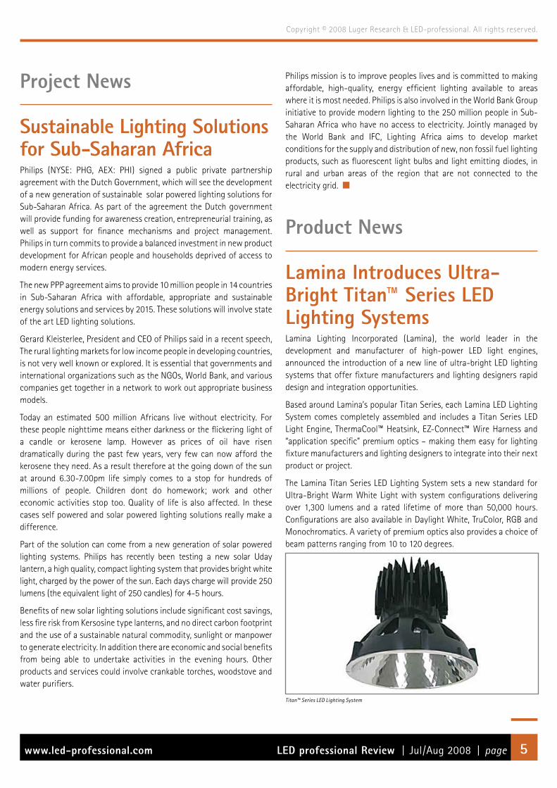
Lamina Introduces Ultra-Bright Titan™ Series LED Lighting Systems Lamina Lighting Incorporated (Lamina), the world leader in the development and manufacturer of high-power LED light engines, announced the introduction of a new line of ultra-bright LED lighting systems that offer fixture manufacturers and lighting designers rapid design and integration opportunities.
Based around Lamina’s popular Titan Series, each Lamina LED Lighting System comes completely assembled and includes a Titan Series LED Light Engine, ThermaCool™ Heatsink, EZ-Connect™ Wire Harness and “application specific” premium optics – making them easy for lighting fixture manufacturers and lighting designers to integrate into their next product or project.
The Lamina Titan Series LED Lighting System sets a new standard for Ultra-Bright Warm White Light with system configurations delivering over 1,300 lumens and a rated lifetime of more than 50,000 hours. Configurations are also available in Daylight White, TruColor, RGB and Monochromatics. A variety of premium optics also provides a choice of beam patterns ranging from 10 to 120 degrees.
Titan™ Series LED Lighting System

LED professional Review | Jul/Aug 2008 | pagewww.led-professional.com 6
Copyright © 2008 Luger Research & LED-professional. All rights reserved.
The Titan Series LED Lighting System features:•Long-life greater than 50,000 hours•High CRI 80+• Cool beam - no UV or IR•Available in Warm White (3050K), Daylight White (4700K), TruColor
(3050K) and Monochrome•Dimmable• RoHS Compliant• No Lead• No Mercury
“Until now many lighting fixture manufactures and lighting designers have had to engineer and design around each individual component in order to take full advantage of all that LED lighting technology can offer,” said Dan Polito, vice president of marketing at Lamina. “With our Titan Series LED Lighting System they can now create an LED lighting delivery system from a wide selection of available configurations.”
The variety of general illumination applications for the Lamina Titan Series LED Lighting System is extensive and includes, stage and studio, architainment, low-voltage landscape, track heads, portable and solar lighting, commercial and residential recess down lighting, and street and perimeter lighting systems.
Polito also noted that each Lamina Titan Series LED Lighting System emits no heat (infrared) or ultraviolet radiation, is readily dimmable, and contain no mercury (as do fluorescent lamps) or lead. As are all Lamina LED products, the Titan Series LED Lighting System is fully compliant with the EU’s RoHS Directive restricting mercury, lead, cadmium and other hazardous substances.
Synergy™ LED MR-16 Lamps: World’s Most Efficient LED MR-16Synergy by USHIO: The culmination of USHIO’s breakthrough combination of patented optical technology, LED packaging techniques, unique electronics and superior thermal management in the World’s First Truly Usable LED MR-16 Product!
From the world leader in MR-16 lamp technology comes the world’s most efficient solid state LED MR-16 lamp. Synergy’s state-of-the-art technology allows this 4W LED MR-16 to directly replace 20-25W halogen MR-16s. No false claims, just outstanding performance that yields 80% energy savings. In fact, Synergy is the first LED MR-16 lamp to meet the efficiency requirements of California’s stringent Title 24 regulations.
Rated at 50,000 hours, Synergy has a true life rating of more than 10 times that of standard MR-16 lamps on the market today. Synergy is the premium choice for those applications where frequency of lamp changes and cost of ownership are significant factors.
USHIO Synergy™ LED MR-16 Lamp: Available in Spot (12°), Narrow Flood (24°), Flood (34°) and Wide Flood (50°) beam spreads
Features & Benefits:• 80% Energy Savings vs. Halogen MR-16• Long Life: 50,000 Hours• Direct Replacement for Halogen MR-16• Application Grade: True Usable Light• Fully Dimmable• Cool Beam – Cool Operation• Application Friendly: UV Free, IR Free• Environmentally Friendly: Mercury Free, Lead Free, RoHS Compliant
80% Savings On Electricity with LED Street LightingThe latest developments in high power LED lighting technology offer a viable alternative to conventional street lighting with energy savings of up to 80% and a considerable reduction in carbon emissions.
Joliet Technology has recently launched a range of street lights based on high power LED (light emitting diode) technology. The range offers a selection of LED mast head lamp units designed to replace existing sodium and metal halide street lamps, a simple LED light bulb that fits standard E40 bulb holders, a specially designed tunnel light for underground applications, and a solar powered street light system which is totally independent of mains power.
Joliet Masthead JOL4 LED: 112W four module lamp to replace a 250W sodium HP lamp
LED professional Review | Jul/Aug 2008 | pagewww.led-professional.com 7
Copyright © 2008 Luger Research & LED-professional. All rights reserved.
Switching to LED street lights offers up to 80% savings on power consumption and ensures a complete return on investment in less than 17 months with colossal savings over the 10 year life of the product. Resultant reductions in harmful Co2 and So2 emissions are proportional.
Comparison between a conventional 400W sodium HP lamp and an equivalent JOL168W high power LED lamp based on 12 hours usage per 24 hour period shows a saving of 12.25kWh (Sodium HP power daily consumption = 14.83kWh, Joliet 168W high power LED daily consumption = 2.58kWh)
At current European average power costs this saving amounts to around 550 Euros per lamp, per year. A saving of 55,000 Euros per year per 100 lights in operation.
Conventional sodium HP or metal halide lamps have a life span of around one year requiring at least annual replacement and maintenance. Joliet high power LED lights require no regular maintenance further increasing savings on replacement bulbs, access equipment and labour costs. New installations benefit from a substantial reduction in the cost of expensive heavy duty cable required for sodium lighting.
The exceptional photometric properties of Joliet high power LED street lights, in addition to offering a bright, natural light colour, provide a uniform rectangular beam pattern (40x16 meters at 12 meter height) that is 50% brighter and 50% larger than the oval beam pattern produced by a conventional lamp. This highly focused beam pattern allows LED lights to be spaced at much wider intervals than sodium lights increasing still further the savings achievable in initial investment requirement and operating costs.
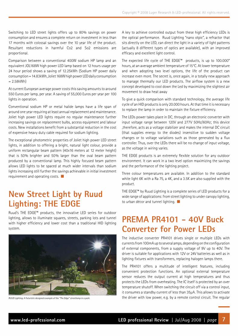
New Street Light by Ruud Lighting: THE EDGERuud’s THE EDGE™ products, the innovative LED series for outdoor lighting, allows to illuminate squares, streets, parking lots and tunnel with higher efficiency and lower cost than a traditional HID lighting system.
RUUD Lighting: A futuristic designed example of the “The Edge” streetlamp in a park.
A key to achieve controlled output from these high efficiency LEDs is the optical performance. Ruud Lighting “nano otpic”, a refractor that sits directly on the LED, can direct the light in a variety of light patterns (actually 8 different types of optics are available), with an improved efficacy and excellent light control.
The expected life cycle of THE EDGE™ products, is up to 100.000* hours, at an average ambient temperature of 15°C. At lower temperature and when adopting two level options, the life of the product can increase even more. The secret is, once again, in a totally new approach to manage thermally our LED products. The airflow system is a new concept developed to cool down the Led by maximizing the slightest air movement to draw heat away
To give a quick comparison with standard technology, the average life cycle of an HID products is only 20.000 hours. At that time it is necessary to replace the lamp in order to maintain the fixture efficiency.
The LEDs power takes place in DC, through an electronic converter with input voltage range between 120V and 277V 50Hz/60Hz; this device ,therefore, acts as a voltage stabilizer and makes the internal DC circuit (that supplies energy to the diodes) insensitive to sudden voltage changes or to voltage variations such as those generated by a flux controller. Thus, over the LEDs there will be no change of input voltage, as the voltage in wiring varies.
THE EDGE products is an extremely flexible solution for any outdoor environment. It can work in a two level option maximizing the savings and the performance of the lighting project.
Three colour temperatures are available. In addition to the standard white light 6K with a Ra 75, a 4K, and a 3.5K are also supplied with the product.
THE EDGE™ by Ruud Lighting is a complete series of LED products for a wide range of applications: from street lighting to under canopy lighting, to urban décor and tunnel lighting.
PREMA PR4101 - 40V Buck Converter for Power LEDsThe inductive converter PR4101 drives single or multiple LEDs with currents from 100mA up to several amps, depending on the configuration of external components, from a supply voltage of 9V up to 40V. The driver is suitable for applications with 12V or 24V batteries as well as in lighting fixtures with transformers, replacing halogen lamps there.
The PR4101 offers a multitude of intelligent features, including convenient protection functions. An optional external temperature sensor reduces the output current at high temperatures and thus protects the LEDs from overheating. The IC itself is protected by an over temperature shutoff. When switching the circuit off via a control input, it consumes a standby current of less than 35µA. This allows to activate the driver with low power, e.g. by a remote control circuit. The regular
LED professional Review | Jul/Aug 2008 | pagewww.led-professional.com 8
Copyright © 2008 Luger Research & LED-professional. All rights reserved.
operation voltage of PR4101 ranges from 9 to 40V DC. With only a few additional components operation is also possible from 12V or 24V AC. PR4101’s VDI input uses the phase-cut supply from conventional dimmers as duty cycle for the output current.
Typical application with PREMA PR4101 for minimum PCB size
A simple circuit allows switching the light softly. The LED current is easily adjusted with an external sense resistor or with a pulse-width modulated signal on the PWM input with a duty cycle between 2 and 100%.
The efficiency varies between 70% and 95%, depending on the respective operating conditions. Furthermore, the EMI is improved by variation of the converter frequency over a range of 10%.
The PR4101 is especially suited for LCD backlighting and other LED operated lighting. Depending on the application different packages are available, the SO14 (PR4101A) offering all features and the SO8 package (PR4101B) for smaller sized PCBs without power-down and PWM function.
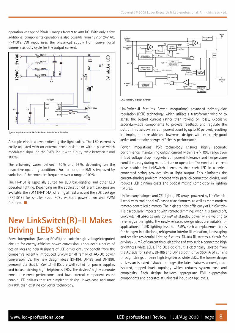
New LinkSwitch(R)-II Makes Driving LEDs SimplePower Integrations (Nasdaq:POWI), the leader in high-voltage integrated circuits for energy-efficient power conversion, announced a series of design ideas to help designers of LED driver circuitry benefit from the company’s recently introduced LinkSwitch-II family of AC-DC power conversion ICs. The new design ideas (DI-184, DI-185 and DI-186), demonstrate that LinkSwitch-II ICs are well suited for power supplies and ballasts driving high-brightness LEDs. The devices’ highly accurate constant-current performance and low external component count enable LED ballasts that are simpler to design, lower-cost, and more durable than existing converter technology.
LinkSwitch(R)-II block diagram
LinkSwitch-II features Power Integrations’ advanced primary-side regulation (PSR) technology, which utilizes a transformer winding to sense the output current rather than relying on lossy, expensive secondary-side components to provide feedback and regulate the output. This cuts system component count by up to 30 percent, resulting in simpler, more reliable and lowercost designs with extremely good active and standby energy-efficiency performance.
Power Integrations’ PSR technology ensures highly accurate performance, maintaining output current within a +/- 10% range even if load voltage drop, magnetic component tolerance and temperature conditions vary during manufacture or operation. The constant-current drive enabled by LinkSwitch-II ensures that each LED in a series-connected string provides similar light output. This eliminates the current-sharing problem inherent with parallel-connected diodes, and reduces LED binning costs and optical mixing complexity in lighting fixtures.
Unlike many halogen and CFL lights, LED arrays powered by LinkSwitch-II work with traditional AC-based triac dimmers, as well as more modern remote-controlled dimmers. The high standby efficiency of LinkSwitch-II is particularly important with remote dimming; when it is turned off, LinkSwitch-II absorbs only 30 mW of standby power while waiting to re-energize the lights. The newly released design ideas are suitable for applications of LED lighting less than 5.5W, such as replacement bulbs for halogen installations, refrigerator interior illumination, landscaping and smaller residential lighting fixtures. DI-184 illustrates a circuit for driving 700mA of current through strings of two series-connected high brightness white LEDs. The DC side circuit is electrically isolated from the AC side for safety. DI-185 and DI-186 both drive 350mA of current through strings of three high brightness white LEDs. The former design utilizes an isolated flyback topology, the later features a novel, non-isolated, tapped buck topology which reduces system cost and complexity. Each design includes appropriate EMI suppression components and operates at universal input voltage levels.
LED professional Review | Jul/Aug 2008 | pagewww.led-professional.com 9
Copyright © 2008 Luger Research & LED-professional. All rights reserved.
Comments Doug Bailey, vice president of marketing at Power Integrations: “By using LinkSwitch-II, lighting designers are benefiting from a power supply solution that matches the LED’s efficiency, longevity and safety. The elimination of lossy secondary-side circuitry enabled by primary-side regulation, in combination with our EcoSmart energy-efficiency technology, results in a highly efficient and cost-effective offline LED driver.”
Mr. Bailey continues: “LinkSwitch-II has integrated safety features which ensure that the power supply shuts down if the feedback loop is broken due to external component failure. The device also monitors its own temperature and shuts itself down to prevent the luminary from overheating in fault conditions or due to poor fixture installation, adding a layer of safety for system designers and end users. LinkSwitch-II also lives up to Power Integrations’ reputation for reliability and the 700 V MOSFET inside the LinkSwitch-II provides an increased level of protection against line surges that can cause traditional bulbs to fail.”
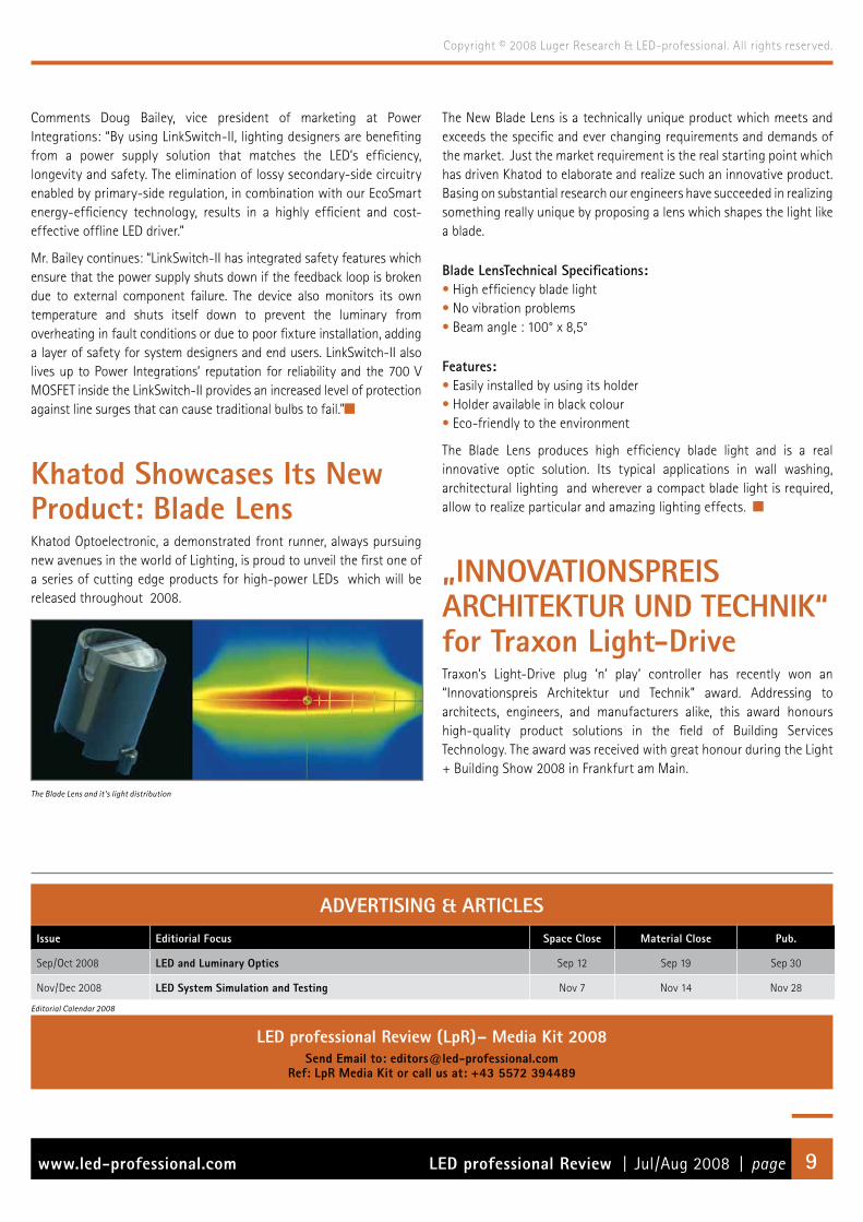
Khatod Showcases Its New Product: Blade LensKhatod Optoelectronic, a demonstrated front runner, always pursuing new avenues in the world of Lighting, is proud to unveil the first one of a series of cutting edge products for high-power LEDs which will be released throughout 2008.
The Blade Lens and it’s light distribution
The New Blade Lens is a technically unique product which meets and exceeds the specific and ever changing requirements and demands of the market. Just the market requirement is the real starting point which has driven Khatod to elaborate and realize such an innovative product. Basing on substantial research our engineers have succeeded in realizing something really unique by proposing a lens which shapes the light like a blade.
Blade LensTechnical Specifications:• High efficiency blade light• No vibration problems• Beam angle : 100° x 8,5°
Features:• Easily installed by using its holder• Holder available in black colour• Eco-friendly to the environment
The Blade Lens produces high efficiency blade light and is a real innovative optic solution. Its typical applications in wall washing, architectural lighting and wherever a compact blade light is required, allow to realize particular and amazing lighting effects.
„INNOVATIONSPREIS ARCHITEKTUR UND TECHNIK“ for Traxon Light-Drive Traxon’s Light-Drive plug ‘n’ play’ controller has recently won an “Innovationspreis Architektur und Technik” award. Addressing to architects, engineers, and manufacturers alike, this award honours high-quality product solutions in the field of Building Services Technology. The award was received with great honour during the Light + Building Show 2008 in Frankfurt am Main.
LED professional Review (LpR)– Media Kit 2008Send Email to: [email protected]
Ref: LpR Media Kit or call us at: +43 5572 394489
Issue Editiorial Focus Space Close Material Close Pub.
Sep/Oct 2008 LED and Luminary Optics Sep 12 Sep 19 Sep 30
Nov/Dec 2008 LED System Simulation and Testing Nov 7 Nov 14 Nov 28
ADVERTISING & ARTICLES
Editorial Calendar 2008

LED professional Review | Jul/Aug 2008 | pagewww.led-professional.com 10
Copyright © 2008 Luger Research & LED-professional. All rights reserved.
Light-Drive functions
The Traxon Light-Drive ‘plug ‘n’ play’ controller, with a stylish sleek design, can be applied for RGB LED fixtures in both professional and consumer markets. The userfriendly Light-Drive allows users to take control of lighting mood in two or more lighting zones. Users can control lighting using the uniquely incorporated functions including colour tuning, brightness setting, colour preview, speed control, play/pause light show, create spaces with light, white mode, remote server access, sequence function, and i-wash function. On top of that, the Light-Drive can also remember up to six memory settings, providing users the convenience of taking control at the touch of a button. Users may also use the Traxon Light-Drive IR Remote Control to recall all functions on the Light-Drive from a distance.
Advanced FR4 PCB Material and High Performance Heat Sink PCBIn order to get a better heat dissipation within the PCB, SIIX Corp. has developed an advanced SIIX Corp. FR4 PCB material. This advanced material has a better thermal performance compared to standard aluminium MCPCB. Standard aluminium MCPCB with standard dielectric achieves 9 K/W. With the advanced SIIX Corp. FR4 PCB material it is possible to achieve 7K/W. This advanced material is also lighter compared to aluminium MCPCB. The most important advantage is the price performance of the advanced SIIX Corp. FR4 PCB material. In spite of the above mentioned advantages the advanced SIIX Corp.FR4 PCB material is also cheaper than aluminium MCPCB.
For the efficient production SIIX Corp. has developed an advanced soldering process which can be used for all kinds of temperature sensible parts. This advanced assembly process is called Magical Cool Soldering Process (henceforth M.C.S.P.) and contains an efficient soldering process, a special solder and offers a very good thermal connection and a reliable solder connection. The good thermal
connectivity and the high reliability of the solder connection can be achieved by the M.C.S.P. If you use today a laser or robot soldering process the soldering time can be drastically minimized by the advanced SIIX Corp. M.C.S.P. The process is very efficient as all LED’s and all kind of other devices can be soldered in one step. Therefore this solution provides market competitiveness in comparison to a laser or robot assembly process.
The advanced SIIX Corp. FR4 PCB material and the advanced SIIX Corp. M.C.S.P. has already achieved excellent test results. In order to test the solder joint reliability a 1000 hours high temperature cycle test (-40°C up to +125°C) and an X-ray analysis has been passedwith success.
Furthermore SIIX Corp. has also developed an advanced PCB surface. With this development the LED light reflection could be maximized and the light reflection is stable over a long time. The benefits of this development has a impact on the LED application as it offers a high LED light efficiency which results in a longer life time as less energy for the same light is required.
New High Performance Heat Sink PCB
The latest advanced technology innovation by SIIX Corp. is related to the Heat Sink PCB. With this advanced technology innovation the LED’s can be soldered directly at the High Performance Heat Sink PCB (henceforth A.H.S. PCB) with the SIIX Corp. M.C.S.P. solution. This solution offers the best thermal connectivity as the LED’s are directly soldered on the A.H.S. PCB and no separate PCB thermal adhesive is required. As the A.H.S. PCB is very efficient the dimension can be reduced significantly which results also in a reduction of the weight. In addition the A.H.S PCB induces a lower LED surface temperature compared to a standard aluminium PCB/Heat Sink solution. The advanced solution of SIIX Corp. can be adapted to the customer’s specific requirements. With the SIIX Corp. A.H.S. PCB mixed assembly all kind of devices and components can be soldered on this A.H.S PCB.
The A.H.S PCB provides very good cost competitiveness compared to standard aluminium MCPCB including heat sink solution and gives architects and designers an attractive and efficient solution. SIIX Corp. is offering the EMS where all advanced technologies can be selected according to the customer’s specific requirements in order to optimise the customer’s application.
LED professional Review | Jul/Aug 2008 | pagewww.led-professional.com 11
Copyright © 2008 Luger Research & LED-professional. All rights reserved.
Research News
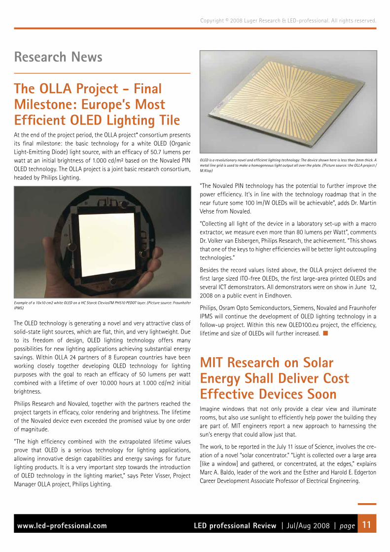
The OLLA Project - Final Milestone: Europe’s Most Efficient OLED Lighting TileAt the end of the project period, the OLLA project* consortium presents its final milestone: the basic technology for a white OLED (Organic Light-Emitting Diode) light source, with an efficacy of 50.7 lumens per watt at an initial brightness of 1.000 cd/m² based on the Novaled PIN OLED technology. The OLLA project is a joint basic research consortium, headed by Philips Lighting.
Example of a 10x10 cm2 white OLED on a HC Starck CleviosTM PH510 PEDOT layer. (Picture source: Fraunhofer IPMS)
The OLED technology is generating a novel and very attractive class of solid-state light sources, which are flat, thin, and very lightweight. Due to its freedom of design, OLED lighting technology offers many possibilities for new lighting applications achieving substantial energy savings. Within OLLA 24 partners of 8 European countries have been working closely together developing OLED technology for lighting purposes with the goal to reach an efficacy of 50 lumens per watt combined with a lifetime of over 10.000 hours at 1.000 cd/m2 initial brightness.
Philips Research and Novaled, together with the partners reached the project targets in efficacy, color rendering and brightness. The lifetime of the Novaled device even exceeded the promised value by one order of magnitude.
“The high efficiency combined with the extrapolated lifetime values prove that OLED is a serious technology for lighting applications, allowing innovative design capabilities and energy savings for future lighting products. It is a very important step towards the introduction of OLED technology in the lighting market,” says Peter Visser, Project Manager OLLA project, Philips Lighting.
OLED is a revolutionary novel and efficient lighting technology: The device shown here is less than 2mm thick. A metal line grid is used to make a homogeneous light output all over the plate. (Picture source: the OLLA project / M.Klop)
“The Novaled PIN technology has the potential to further improve the power efficiency. It’s in line with the technology roadmap that in the near future some 100 lm/W OLEDs will be achievable”, adds Dr. Martin Vehse from Novaled.
“Collecting all light of the device in a laboratory set-up with a macro extractor, we measure even more than 80 lumens per Watt”, comments Dr. Volker van Elsbergen, Philips Research, the achievement. “This shows that one of the keys to higher efficiencies will be better light outcoupling technologies.”
Besides the record values listed above, the OLLA project delivered the first large sized ITO-free OLEDs, the first large-area printed OLEDs and several ICT demonstrators. All demonstrators were on show in June 12, 2008 on a public event in Eindhoven.
Philips, Osram Opto Semiconductors, Siemens, Novaled and Fraunhofer IPMS will continue the development of OLED lighting technology in a follow-up project. Within this new OLED100.eu project, the efficiency, lifetime and size of OLEDs will further increased.
MIT Research on Solar Energy Shall Deliver Cost Effective Devices SoonImagine windows that not only provide a clear view and illuminate rooms, but also use sunlight to efficiently help power the building they are part of. MIT engineers report a new approach to harnessing the sun’s energy that could allow just that.
The work, to be reported in the July 11 issue of Science, involves the cre-ation of a novel “solar concentrator.” “Light is collected over a large area [like a window] and gathered, or concentrated, at the edges,” explains Marc A. Baldo, leader of the work and the Esther and Harold E. Edgerton Career Development Associate Professor of Electrical Engineering.
LED professional Review | Jul/Aug 2008 | pagewww.led-professional.com 12
Copyright © 2008 Luger Research & LED-professional. All rights reserved.
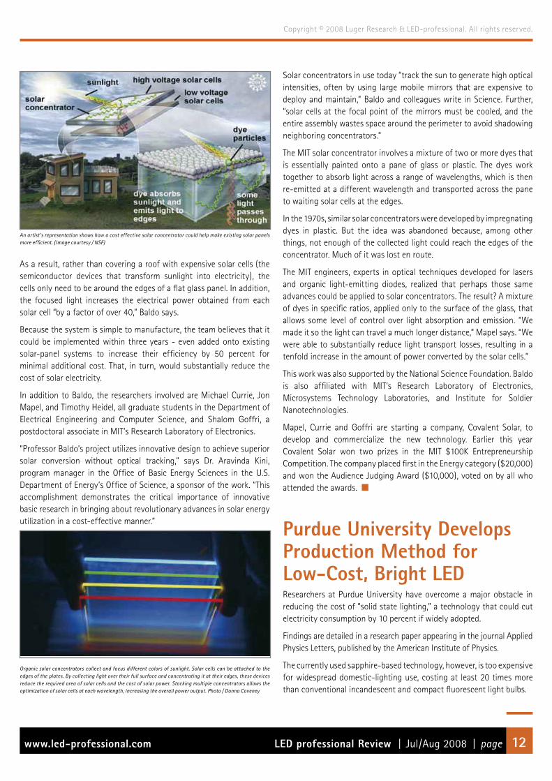
An artist’s representation shows how a cost effective solar concentrator could help make existing solar panels more efficient. (Image courtesy / NSF)
As a result, rather than covering a roof with expensive solar cells (the semiconductor devices that transform sunlight into electricity), the cells only need to be around the edges of a flat glass panel. In addition, the focused light increases the electrical power obtained from each solar cell “by a factor of over 40,” Baldo says.
Because the system is simple to manufacture, the team believes that it could be implemented within three years - even added onto existing solar-panel systems to increase their efficiency by 50 percent for minimal additional cost. That, in turn, would substantially reduce the cost of solar electricity.
In addition to Baldo, the researchers involved are Michael Currie, Jon Mapel, and Timothy Heidel, all graduate students in the Department of Electrical Engineering and Computer Science, and Shalom Goffri, a postdoctoral associate in MIT’s Research Laboratory of Electronics.
“Professor Baldo’s project utilizes innovative design to achieve superior solar conversion without optical tracking,” says Dr. Aravinda Kini, program manager in the Office of Basic Energy Sciences in the U.S. Department of Energy’s Office of Science, a sponsor of the work. “This accomplishment demonstrates the critical importance of innovative basic research in bringing about revolutionary advances in solar energy utilization in a cost-effective manner.”
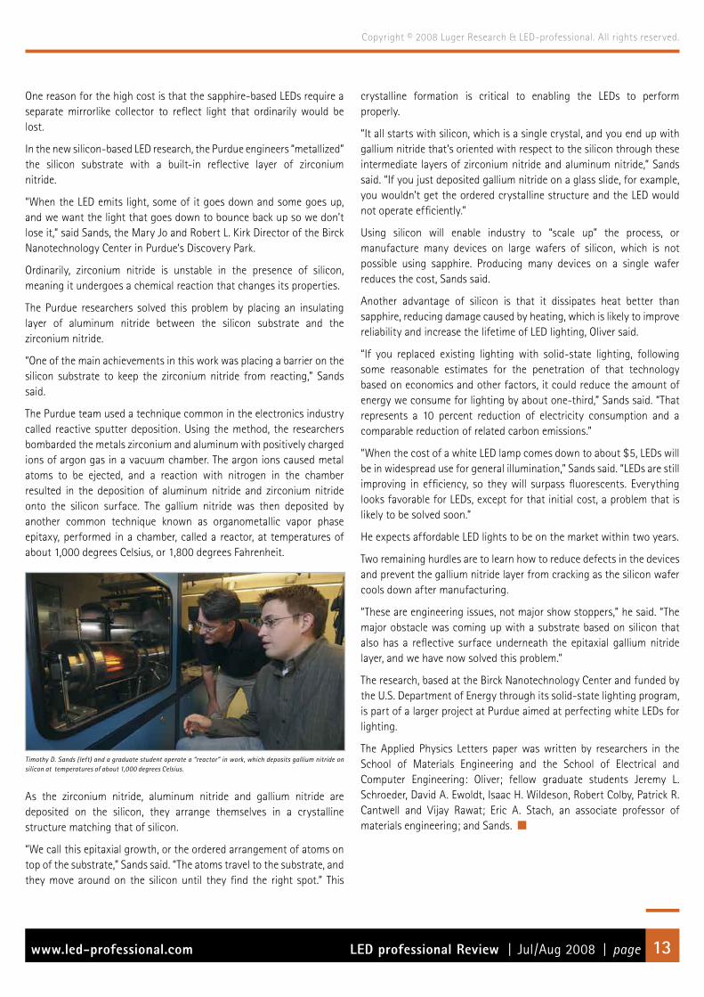
Organic solar concentrators collect and focus different colors of sunlight. Solar cells can be attached to the edges of the plates. By collecting light over their full surface and concentrating it at their edges, these devices reduce the required area of solar cells and the cost of solar power. Stacking multiple concentrators allows the optimization of solar cells at each wavelength, increasing the overall power output. Photo / Donna Coveney
Solar concentrators in use today “track the sun to generate high optical intensities, often by using large mobile mirrors that are expensive to deploy and maintain,” Baldo and colleagues write in Science. Further, “solar cells at the focal point of the mirrors must be cooled, and the entire assembly wastes space around the perimeter to avoid shadowing neighboring concentrators.”
The MIT solar concentrator involves a mixture of two or more dyes that is essentially painted onto a pane of glass or plastic. The dyes work together to absorb light across a range of wavelengths, which is then re-emitted at a different wavelength and transported across the pane to waiting solar cells at the edges.
In the 1970s, similar solar concentrators were developed by impregnating dyes in plastic. But the idea was abandoned because, among other things, not enough of the collected light could reach the edges of the concentrator. Much of it was lost en route.
The MIT engineers, experts in optical techniques developed for lasers and organic light-emitting diodes, realized that perhaps those same advances could be applied to solar concentrators. The result? A mixture of dyes in specific ratios, applied only to the surface of the glass, that allows some level of control over light absorption and emission. “We made it so the light can travel a much longer distance,” Mapel says. “We were able to substantially reduce light transport losses, resulting in a tenfold increase in the amount of power converted by the solar cells.”
This work was also supported by the National Science Foundation. Baldo is also affiliated with MIT’s Research Laboratory of Electronics, Microsystems Technology Laboratories, and Institute for Soldier Nanotechnologies.
Mapel, Currie and Goffri are starting a company, Covalent Solar, to develop and commercialize the new technology. Earlier this year Covalent Solar won two prizes in the MIT $100K Entrepreneurship Competition. The company placed first in the Energy category ($20,000) and won the Audience Judging Award ($10,000), voted on by all who attended the awards.
Purdue University Develops Production Method for Low-Cost, Bright LED Researchers at Purdue University have overcome a major obstacle in reducing the cost of “solid state lighting,” a technology that could cut electricity consumption by 10 percent if widely adopted.
Findings are detailed in a research paper appearing in the journal Applied Physics Letters, published by the American Institute of Physics.
The currently used sapphire-based technology, however, is too expensive for widespread domestic-lighting use, costing at least 20 times more than conventional incandescent and compact fluorescent light bulbs.
LED professional Review | Jul/Aug 2008 | pagewww.led-professional.com 13
Copyright © 2008 Luger Research & LED-professional. All rights reserved.
One reason for the high cost is that the sapphire-based LEDs require a separate mirrorlike collector to reflect light that ordinarily would be lost.
In the new silicon-based LED research, the Purdue engineers “metallized” the silicon substrate with a built-in reflective layer of zirconium nitride.
“When the LED emits light, some of it goes down and some goes up, and we want the light that goes down to bounce back up so we don’t lose it,” said Sands, the Mary Jo and Robert L. Kirk Director of the Birck Nanotechnology Center in Purdue’s Discovery Park.
Ordinarily, zirconium nitride is unstable in the presence of silicon, meaning it undergoes a chemical reaction that changes its properties.
The Purdue researchers solved this problem by placing an insulating layer of aluminum nitride between the silicon substrate and the zirconium nitride.
“One of the main achievements in this work was placing a barrier on the silicon substrate to keep the zirconium nitride from reacting,” Sands said.
The Purdue team used a technique common in the electronics industry called reactive sputter deposition. Using the method, the researchers bombarded the metals zirconium and aluminum with positively charged ions of argon gas in a vacuum chamber. The argon ions caused metal atoms to be ejected, and a reaction with nitrogen in the chamber resulted in the deposition of aluminum nitride and zirconium nitride onto the silicon surface. The gallium nitride was then deposited by another common technique known as organometallic vapor phase epitaxy, performed in a chamber, called a reactor, at temperatures of about 1,000 degrees Celsius, or 1,800 degrees Fahrenheit.
Timothy D. Sands (left) and a graduate student operate a “reactor” in work, which deposits gallium nitride on silicon at temperatures of about 1,000 degrees Celsius.
As the zirconium nitride, aluminum nitride and gallium nitride are deposited on the silicon, they arrange themselves in a crystalline structure matching that of silicon.
“We call this epitaxial growth, or the ordered arrangement of atoms on top of the substrate,” Sands said. “The atoms travel to the substrate, and they move around on the silicon until they find the right spot.” This
crystalline formation is critical to enabling the LEDs to perform properly.
“It all starts with silicon, which is a single crystal, and you end up with gallium nitride that’s oriented with respect to the silicon through these intermediate layers of zirconium nitride and aluminum nitride,” Sands said. “If you just deposited gallium nitride on a glass slide, for example, you wouldn’t get the ordered crystalline structure and the LED would not operate efficiently.”
Using silicon will enable industry to “scale up” the process, or manufacture many devices on large wafers of silicon, which is not possible using sapphire. Producing many devices on a single wafer reduces the cost, Sands said.
Another advantage of silicon is that it dissipates heat better than sapphire, reducing damage caused by heating, which is likely to improve reliability and increase the lifetime of LED lighting, Oliver said.
“If you replaced existing lighting with solid-state lighting, following some reasonable estimates for the penetration of that technology based on economics and other factors, it could reduce the amount of energy we consume for lighting by about one-third,” Sands said. “That represents a 10 percent reduction of electricity consumption and a comparable reduction of related carbon emissions.”
“When the cost of a white LED lamp comes down to about $5, LEDs will be in widespread use for general illumination,” Sands said. “LEDs are still improving in efficiency, so they will surpass fluorescents. Everything looks favorable for LEDs, except for that initial cost, a problem that is likely to be solved soon.”
He expects affordable LED lights to be on the market within two years.
Two remaining hurdles are to learn how to reduce defects in the devices and prevent the gallium nitride layer from cracking as the silicon wafer cools down after manufacturing.
“These are engineering issues, not major show stoppers,” he said. “The major obstacle was coming up with a substrate based on silicon that also has a reflective surface underneath the epitaxial gallium nitride layer, and we have now solved this problem.”
The research, based at the Birck Nanotechnology Center and funded by the U.S. Department of Energy through its solid-state lighting program, is part of a larger project at Purdue aimed at perfecting white LEDs for lighting.
The Applied Physics Letters paper was written by researchers in the School of Materials Engineering and the School of Electrical and Computer Engineering: Oliver; fellow graduate students Jeremy L. Schroeder, David A. Ewoldt, Isaac H. Wildeson, Robert Colby, Patrick R. Cantwell and Vijay Rawat; Eric A. Stach, an associate professor of materials engineering; and Sands.
LED professional Review | Jul/Aug 2008 | pagewww.led-professional.com 14
Copyright © 2008 Luger Research & LED-professional. All rights reserved.
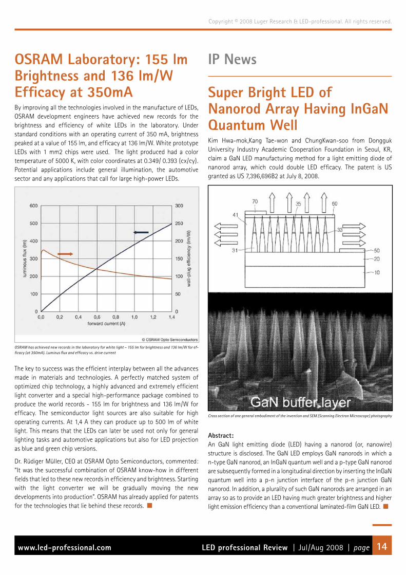
OSRAM Laboratory: 155 lm Brightness and 136 lm/W Efficacy at 350mABy improving all the technologies involved in the manufacture of LEDs, OSRAM development engineers have achieved new records for the brightness and efficiency of white LEDs in the laboratory. Under standard conditions with an operating current of 350 mA, brightness peaked at a value of 155 lm, and efficacy at 136 lm/W. White prototype LEDs with 1 mm2 chips were used. The light produced had a color temperature of 5000 K, with color coordinates at 0.349/ 0.393 (cx/cy). Potential applications include general illumination, the automotive sector and any applications that call for large high-power LEDs.
OSRAM has achieved new records in the laboratory for white light – 155 lm for brightness and 136 lm/W for ef-ficacy (at 350mA). Luminus flux and efficacy vs. drive current
The key to success was the efficient interplay between all the advances made in materials and technologies. A perfectly matched system of optimized chip technology, a highly advanced and extremely efficient light converter and a special high-performance package combined to produce the world records - 155 lm for brightness and 136 lm/W for efficacy. The semiconductor light sources are also suitable for high operating currents. At 1,4 A they can produce up to 500 lm of white light. This means that the LEDs can later be used not only for general lighting tasks and automotive applications but also for LED projection as blue and green chip versions.
Dr. Rüdiger Müller, CEO at OSRAM Opto Semiconductors, commented: “It was the successful combination of OSRAM know-how in different fields that led to these new records in efficiency and brightness. Starting with the light converter we will be gradually moving the new developments into production”. OSRAM has already applied for patents for the technologies that lie behind these records.
IP News
Super Bright LED of Nanorod Array Having InGaN Quantum WellKim Hwa-mok,Kang Tae-won and ChungKwan-soo from Dongguk University Industry Academic Cooperation Foundation in Seoul, KR, claim a GaN LED manufacturing method for a light emitting diode of nanorod array, which could double LED efficacy. The patent is US granted as US 7,396,696B2 at July 8, 2008.
Cross section of one general embodiment of the invention and SEM (Scanning Electron Microscope) photography
Abstract:An GaN light emitting diode (LED) having a nanorod (or, nanowire) structure is disclosed. The GaN LED employs GaN nanorods in which a n-type GaN nanorod, an InGaN quantum well and a p-type GaN nanorod are subsequently formed in a longitudinal direction by inserting the InGaN quantum well into a p-n junction interface of the p-n junction GaN nanorod. In addition, a plurality of such GaN nanorods are arranged in an array so as to provide an LED having much greater brightness and higher light emission efficiency than a conventional laminated-film GaN LED.
LED professional Review | Jul/Aug 2008 | pagewww.led-professional.com 16
Copyright © 2008 Luger Research & LED-professional. All rights reserved.
Application
City of Kelowna Goes Green with Solar-Powered Area Lighting> Anthony Tisot, President, Carmanah Technologies Corporation
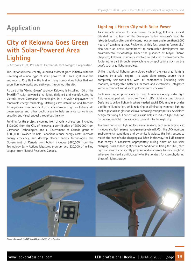
The City of Kelowna recently launched its latest green initiative with the unveiling of a new type of solar powered LED area light near the entrance to City Hall — the first of many stand-alone lights that will soon illuminate parks and pathways throughout the city.
As part of its “Going Green” strategy, Kelowna is installing 100 of the EverGEN™ solar-powered area lights, designed and manufactured by Victoria-based Carmanah Technologies, in a citywide deployment of renewable energy technology. Offering easy installation and freedom from grid-access requirements, the solar-powered lights will illuminate green spaces and other public areas to help enhance convenience, security, and visual appeal throughout the city.
Funding for the project is coming from a variety of sources, including $128,000 from the City of Kelowna, a contribution of $530,000 from Carmanah Technologies, and a Government of Canada grant of $500,000. Provided to help Canadians reduce energy costs, increase energy efficiency, and develop cleaner energy technologies, the Government of Canada contribution includes $480,000 from the Technology Early Actions Measures program and $20,000 of in-kind support from Natural Resources Canada.
Lighting a Green City with Solar PowerAs a suitable location for solar power technology, Kelowna is ideal. Situated in the heart of the Okanagan Valley, Kelowna’s beautiful lakeside location offers mild winters, hot summers and more than 2,000 hours of sunshine a year. Residents of this fast-growing “green city” also share an active commitment to sustainable development and environmental stewardship. Under the guidance of Mayor Sharon Shepherd, Kelowna is actively involved in reducing its environmental footprint, in part through renewable energy applications such as this year’s solar area lighting project.
Unlike traditional lighting technology, each of the new area lights is powered by a solar engine — a stand-alone energy source that’s completely self-contained, with all components (including solar modules, rechargeable batteries, sensors and electronics) integrated within a compact and durable pole-mounted enclosure.
Each solar engine powers one or more luminaires — adjustable light fixtures equipped with energy-efficient LEDs (light emitting diodes). Designed to deliver light only where needed, each LED luminaire provides a uniform illumination, while reducing or eliminating common lighting challenges such as glare or spillover onto adjacent properties. A shielded design featuring full cut-off optics also helps to reduce light pollution by preventing light from escaping upward into the night sky.
To ensure consistent lighting levels in all seasons, each solar engine also includes a built-in energy management system (EMS). The EMS monitors environmental conditions and dynamically adjusts the light output to match the level of solar charging available. In this way, the EMS ensures that energy is conserved appropriately during times of low solar charging (such as low light or winter conditions). Using the EMS, each light can also be intelligently programmed in advance to shine brightest whenever the need is anticipated to be the greatest, for example, during times of highest usage.
Figure 1: Carmanah EverGEN Solar LED streetlight in off and on state

LED professional Review | Jul/Aug 2008 | pagewww.led-professional.com 17
Copyright © 2008 Luger Research & LED-professional. All rights reserved.
As a stand-alone lighting solution, Kelowna’s solar area lights require no trenching, cabling or electrical hook up, so installation is relatively simple. Free from the limitations of grid access, each light can be installed quickly and easily, wherever light is needed. With no bulbs to replace and an LED lifespan of up to 50,000 hours, maintenance is also expected to be minimal.
Figure 3: Preparation of the solar engine for installation at the pole by qualified personnel
Selecting Sites for Solar Powered Lights In choosing suitable locations, the project team started with a list of 200 potential sites, and selected the final 100 spots based on a list of factors including technical and geographic considerations (such as access to sunlight), distribution throughout the community, functional variety, and distance from an existing power supply. The final list identified a variety of buildings, parks, trails, crosswalks, municipal facilities, parking lot kiosks and transit facilities.
Over the next year, Carmanah engineers will work with City of Kelowna staff to monitor the lights and evaluate their performance in field conditions. A data analysis by Natural Resources Canada will also help to assess power savings and reductions to the community’s carbon footprint.
By using the sun’s energy as an alternative power source, Kelowna’s solar-powered LED lights can help the community to reduce its dependency on grid-based electricity, for a clean, economical and maintenance-free lighting alternative. With this wide-scale commitment to renewable energy technology, Kelowna is leading the way as a true innovator, and one of Canada’s leading solar cities.
Figure 2: Area lighting in parks is one domain, where the combination of solar technology and LED technology is today’s best solution

LED professional Review | Jul/Aug 2008 | pagewww.led-professional.com 18
Copyright © 2008 Luger Research & LED-professional. All rights reserved.
Solar LED Street Lighting > Steffen Block, Application Engineer Solid State Lighting (SSL), OSRAM Opto Semiconductors GmbH, Gerhard Walch, Franz Jungwirth, EPS soltec, and Arno Grabher-Meyer, LED professional
It is incredible that about 20% of electricity is used for lighting worldwide and that, for some municipalities, up to 40% of the electricity bills are calculated for street lighting. In today’s environmentally- and budget conscious society, engineers have combined two existing technologies to help reduce energy costs as well as CO2 emissions. This most recent generation of solar LED street lights provides a mature optical design, thoroughly chosen and dimensioned components, and optimized, robust electronics. Subject to these premises, the combination of photovoltaic and LED technology allows for street lighting, pedestrian lighting, park lighting, etc., and shows numerous advantages over conventional systems: lowered maintenance costs, reduced light pollution, reduced CO2 emissions, and an enhanced “green image” for cities, which attracts new investors, companies, and inhabitants.
Solar Street Lights – Basic Requirements and FactsLEDs are ready to enter the (solar) street lighting marketThe new upcoming LED street lights have to fulfill the already existing street lighting standards, e.g. covered in Europe in the standard EN 13201 part 1 to part 4. The intelligent setup of the optoelectronic component LED is an important focus. LED has to be implemented to fulfill the required optical characteristics, together with other necessary aspects, e.g. thermal management, electronic driving, etc. The solar LED street luminaries from EPS soltec provide a reference example that can be also transferred to other luminaries or lighting scenarios.
Street lighting overviewBasically street lighting is meant to ensure road safety, flow of traffic and public safety. The standard EN 13201- part 1 “road lighting - selection of lighting classes“ classifies the streets in different lighting classes:
•ME1-ME6 (Motorized vehicles on main roads separated in mediumdriving speeds (30-60 km/h) or high driving speeds (above 60 km/h)
•CE0-CE5classesspecifymotorizedvehiclesinconflictareaswithlowdriving speeds (5-30 km/h)
•S1-S6classesdefinethesetupforpedestriansorbicycleswithwalkingor low driving speeds for footpaths, emergency lanes, bicycle lanes, parking areas, school yards, etc.
LED powered streetlights are technically already feasible for all lighting scenarios. From an economical standpoint, there’s only a current limitation to the ME1-6 classes with driving speeds with a max. of 60km/h – that means nearly all streets within the city boundaries are already available for LED use. For highways, the required total flux is, at this point in time, too high for an efficient usage of LEDs, due to the significant longer pay back time compared to traditional lighting.
But this will change over the next few years as efficiency (lm/W) increases (>10% per year) and prices (lm/$ or lm/€) decrease (>10% per year). For solar-powered luminaries the actual application fields are classes S3-S6. The limiting factor hereby is the available power from the battery and sun, based on a reasonable size and cost for the photovoltaic (PV) panels. With future increases of LED, PV panel and battery efficiency, solar LED street lights will be more and more available for higher street classes.
How to design a solar streetlightAs a consequence of the EN 13201- part 1 classification and a desired pole-to-pole distance, e.g., max. 25m, the minimum power requirements can be estimated for each street type. The optical design and efficiency of the LED system are crucial for all further calculations. In addition, the daily solar energy input per m2 (Figure 1) over the year for application areas must be taken into account for the dimensioning of the photovoltaic module and battery capacity correctly. Therefore it is also necessary to know the equivalent daily operating time. For most regions a system that can provide energy for 36 hours of operation without being recharged has proven to be adequate.
Figure1: Relative daily solar energy input for every month of the year and relative energy demands for lighting
Advantages of LEDs in (solar) street lightingThere are numerous advantages for LED technology:
•Directedlightoutput→ system efficiency/homogeneous illumination•Lowvoltages→ best fit for solar-powered street lighting•Longandpredictableserviceintervals→ reduced maintenance costs•Reliabilityandlonglifetime→ increased road safety•Dimming→ adjusting to specific ambient light levels •Smallpackagesize→ flexible, flat and compact luminaire design•High-colourrendering→ appearance and safety•LEDcontainsnopollutingmaterials→ easy lamp recycling•Higherlightoutputevenatlowtemperatures
Street illuminationThe standard EN 13201 - part 2 “road lighting - performance requirements” specifies the different definitions with the requirements for each street type. The major requirements to watch for are luminance, illuminance, uniformity (mean to min), limitation of glare, surround ratio and colour rendering. LEDs are able to fulfil the standards of the
LED professional Review | Jul/Aug 2008 | pagewww.led-professional.com 19
Copyright © 2008 Luger Research & LED-professional. All rights reserved.
traditional lighting world and to exceed these requirements with an intelligent application, e.g. achieving a more homogenous illumination by using adapted lenses or reflectors.
Especially for PV applications, the LED is the perfect product choice. The low DC forward voltage of LEDs can be applied with an electronic circuit to the battery power. Alternatively an electronic boost converter can easily be used to achieve a higher DC voltage and to drive more LEDs in series.
Total Cost of Ownership (TCO)The LED + PV solution requires a higher investment in the beginning, but the digging work for the power cable and the energy costs are not applicable. With the long LED lifetime, expensive maintenance work can be decreased, resulting in a benefit for LED over traditional lighting.
The costs comparison is based on 341m road and 30 years: It shows an advantage of € 18882 for the solar streetlight, while providing similar light quality.
Total Cost of Ownership (TCO) in €Pcs. Product Price/Unit Price
Solar Streetlights (StreetSun)
11 Solar Streetlights 2480.-- 27280.--
11 Foundation 300.-- 3300.--
44 Batteries 200.-- 8800.--
22 LED – Modules 240.-- 5280.--
Total: 44660.--
Traditional Streetlights
9 Streetlights 1600.-- 14400.--
1 Digging, 9 foundations, cabling 15058.-- 15058.--
36 Illuminants 51.-- 1836.--
Electricity 32248.-- 32248.--
Total: 63542.--Table1: Total Cost of Ownership comparison for 341m road and equal lighting quality between a solar street light and a traditional street light
This results in a relaxed budget for the municipalities as an average city spends about 40% of its electrical bill on street lighting [1]. The zero-energy consumption of the solar lights additionally helps to fulfill the strong targets of CO2 reduction.
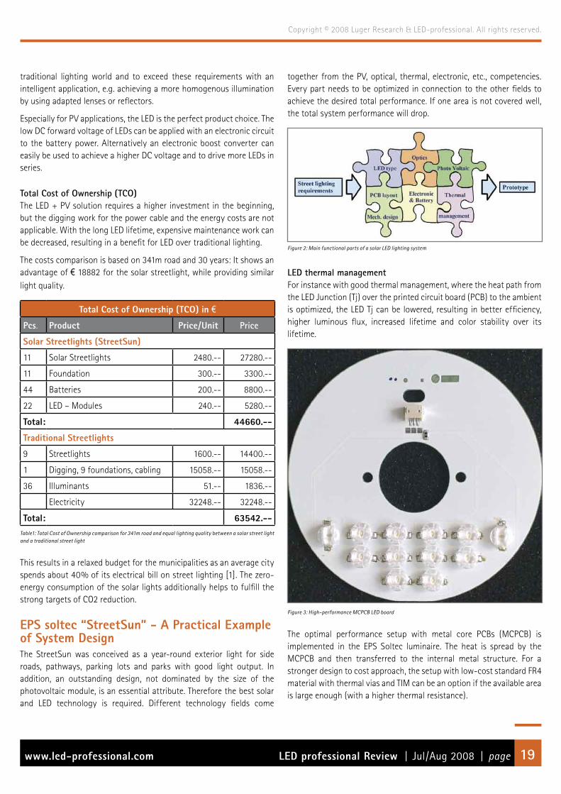
EPS soltec “StreetSun” - A Practical Example of System DesignThe StreetSun was conceived as a year-round exterior light for side roads, pathways, parking lots and parks with good light output. In addition, an outstanding design, not dominated by the size of the photovoltaic module, is an essential attribute. Therefore the best solar and LED technology is required. Different technology fields come
together from the PV, optical, thermal, electronic, etc., competencies. Every part needs to be optimized in connection to the other fields to achieve the desired total performance. If one area is not covered well, the total system performance will drop.
Figure 2: Main functional parts of a solar LED lighting system
LED thermal managementFor instance with good thermal management, where the heat path from the LED Junction (Tj) over the printed circuit board (PCB) to the ambient is optimized, the LED Tj can be lowered, resulting in better efficiency, higher luminous flux, increased lifetime and color stability over its lifetime.
Figure 3: High-performance MCPCB LED board
The optimal performance setup with metal core PCBs (MCPCB) is implemented in the EPS Soltec luminaire. The heat is spread by the MCPCB and then transferred to the internal metal structure. For a stronger design to cost approach, the setup with low-cost standard FR4 material with thermal vias and TIM can be an option if the available area is large enough (with a higher thermal resistance).

LED professional Review | Jul/Aug 2008 | pagewww.led-professional.com 20
Copyright © 2008 Luger Research & LED-professional. All rights reserved.
High-efficient solar power module SM10 - 1800As a benefit to LED technology, the system voltage is 9.6V in order to drive three LEDs in series, requiring a new designed photovoltaic (PV) module. As a concession to the prescribed design, space is limited, resulting in the necessity to provide maximum power density. The monocrystalline PV module has been improved from 20W to 25W recently, according to an efficiency of 17.6%. It consists of 28 specially-connected single cells to fit the nominal voltage requirement. The module assures good efficiency even at low light levels (Figure 3).
Figure 4: Current over-voltage diagram for SM10 – 1800 for different solar irradiation and ambient temperatures
To assure satisfactory results also during the winter month, the capability of the module to deliver enough energy efficiently at low light levels is essential (Figure 4). This is guaranteed by the chosen solar cells from “Ersol”, especially designed for these conditions.
Figure 5: Intermediate daily energy input during a year for the SM10-1800 PV module in Frankfurt, without dec-lination of the module. 42° declination improves these results by 30%. A tracking system leads to an additional improvement of 35%
Choice and dimensioning of batteriesAn energy reserve of up to 36 hours requires 13Ah at 9,6V nominal voltage. The space limitations in the design presented a problem, which was then solved by choosing the correct battery type. Lithium-ion batteries are too expensive and need a costly sensitive monitoring. The first choice is a nickel-metal hydride battery (NiMh), because of the charge- and discharge properties, the thermal behavior (Figure 5), and the achievable number of cycles. Standard NiMh batteries usually work up to 40°C before a protective switch disconnects it. For higher temperature demands, e.g. in tropical regions, a special NiMh battery version that stands up to 65°C is used.
Almost without adaptation, the nominal battery voltage can be used to drive three power LEDs, which are connected in series; therefore, conversion losses are minimized. One special feature, the low LED forward voltage comes with the OSRAM Golden Dragon LED.
The low package weight and small dimension allows placing the batteries in the light head, in the shadow of the solar panel, with the advantage of good cooling capabilities by the wind.
Figure 6: Voltage over-capacity at different temperatures for the 9,5V NiMh battery pack
During the summer months the battery is charged completely every day. During wintertime, where irradiation drops to 20%, the 36-hour energy reserve is sometimes necessary.
The controls – the heart of the systemFor reliable and efficient operation of a solar lighting system, a highly functional electronic control is needed. Day and night recognition, soft-start and dimmed light during dawn, or overload protection for the battery are just some of the requirements for a modern high quality LED street light. As a special challenge, to maximize durability and minimize costs, the reduction of the number of devices was defined as a development goal.
To allow some customized functions, it is necessary to provide a day/night recognition system. Night length is measured by initializing this function 21 hours after the last sunrise. The sunrise is recognized by increased solar-charge-voltage over a predefined threshold. A similar mechanism is implemented to recognize day length.
Battery management is important for system efficiency and battery lifetime. Overcharge protection above 11.3V, as well as deep discharge protection below 9.2V, are implemented to maintain battery lifetime. Several lighting programs are customer-specific programmable, comprising of intelligent programs. The most enhanced program controls the output power of the system to allow lighting through the whole night, depending on the measured energy input over the day, and battery charge status. For special issues, other programs can be implemented incorporating client-specific demands.
LED professional Review | Jul/Aug 2008 | pagewww.led-professional.com 21
Copyright © 2008 Luger Research & LED-professional. All rights reserved.
Figure 7: Schematic of the EPS soltec electronics
right, for increasing the pole distance and spreading the light over the street, supported by the reflector for direct illumination in front of the pole. (Figure 9)
Figure 9: Measurement and simulation results for an existing round shaped reflector
The Elumdat standard (Exchange of Luminaire Data, or alternatively IES file format) from the measurements are used for street lighting simulation in DIALux [2]. The simulation in false color rendering gives a good impression of the light distribution; in this case with the mentioned oval stretch from the OVAL lens. The light is emitted to both sides of the pole through the special existing construction. The pole is located in the middle and provides its light to both sides. This is optimal for parking places or places in general, but for the street light application it means that half of the light is lost to the surrounding grass area (Figure 10).
LED Solar Street Lights – Application for StreetsIntelligent beam shaping is a must for street lighting. Standards have to be fulfilled (e.g. homogenous illumination (Emin to Emax), no disturbing glare or light pollution, etc. Most importantly, all the light has to be brought to the street and not to the surrounding environment.
As the available battery power from the solar cell is limited, the target is not to waste any photons.
Normal available LEDs radiate over a round shape beam in all directions. In contrast, the Golden Dragon OVAL 1W LED LUW W5JM from OSRAM Opto Semiconductors comes with an integrated primary optic. The radiation characteristic is optimized for street lighting applications where the oval beam directs light to the target area. A correlated colour temperature (CCT) of 6500k (Ultra-White (UW)) is the preferred focus for outdoor applications due to higher power efficiency. Additionally, white (LW) with 5600k is possible, and by mixing yellow LEDs to the LUW any other lower CCT can be achieved.
LED implementation process into the solar applicationsThis LED type was implemented 12x in the EPS Soltec luminary design with an existing round reflector. The first measurement of this setup showed the advantage of the OVAL beam with the two coils, left and
fFigure 8: OSRAM Golden Dragon OVAL with primary optic for an oval beam
Schematic just available in LpR digital
or print full version click here

LED professional Review | Jul/Aug 2008 | pagewww.led-professional.com 22
Copyright © 2008 Luger Research & LED-professional. All rights reserved.
Figure 10: DIALux Simulation of the light distribution on the ground with the OVAL lens using the standard reflector
For the no-waste-of-photons approach, the next step was to place all 12 LEDs on one side of the pole and redesign the reflector. The ideal combination was to use the Golden Dragon OVAL LED for the general light distribution along the street and the customized reflector to direct the light towards the street.
Advanced simulation programs, e.g. Lightools, provide the setup for this combination. The high quality reflector material is based on anodized aluminum from Alanod and manufactured, respectively assembled by Alux-Luxar. Both are certified partners in the OSRAM “LED Light for You” partner program to enable a time-to-market approach with dedicated help and services for SSL applications in the different optical, thermal and electronic know-how fields.
Figure 11: Measurement and simulation results for 12 OVAL ARGUS® lens LEDs on one side of the pole and rede-signed reflector
The measurement file (Figure 11) shows directly the coils from OVAL LED and all light on the “basement” is reflected for the illumination in front of the pole on the street.
The Elumdat file from the measurements including the same DIALux simulation of the reference street, shows that the light is now focused on one side of the pole. The highest illumination in the center is achieved with the help from the reflector. Additionally enhanced light distribution
is gained by the reflector and lens combination to reach the required minimum illumination levels. This example shows that, with a pole-to-pole distance of 13m and 5m street width, the standards are fulfilled for street class S6 (Figure 12).
Figure 12: DIALux simulation of the light distribution on the ground with 12 Golden Dragon OVAL LEDs on one side of the pole and redesigned reflector
LED Solar Street Light – Application for Places, Parking Areas, etc.
Different applications have different requirements. This issue was considered in places and parking areas where the required illumination should cover a larger area itself, instead of extending along a small street. The existing round reflector from the beginning already provides this setup.
A non-negligible effect is that every reflection results in a decrease of optical efficiency. To achieve a longer pole distance, it’s more effective to directly spread the light to the side, away from the pole. This performance comes with the Golden Dragon ARGUS® LED. Originally made for backlighting and signage applications, the emitted light is shaped by a primary lens to a side emission pattern for a homogenous backlighting at a short height.
Figure 14: Measurement and simulation results for Golden Dragon ARGUS® LEDs with round reflector
Figure 13: OSRAM Golden Dragon ARGUS® for a round beam
LED professional Review | Jul/Aug 2008 | pagewww.led-professional.com 23
Copyright © 2008 Luger Research & LED-professional. All rights reserved.
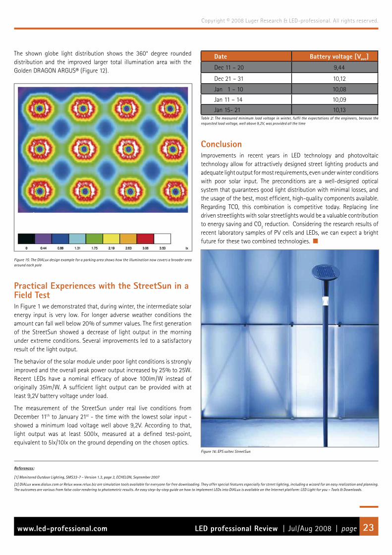
The shown globe light distribution shows the 360° degree rounded distribution and the improved larger total illumination area with the Golden DRAGON ARGUS® (Figure 12).
Figure 15: The DIALux design example for a parking area shows how the illumination now covers a broader area around each pole
Practical Experiences with the StreetSun in a Field TestIn Figure 1 we demonstrated that, during winter, the intermediate solar energy input is very low. For longer adverse weather conditions the amount can fall well below 20% of summer values. The first generation of the StreetSun showed a decrease of light output in the morning under extreme conditions. Several improvements led to a satisfactory result of the light output.
The behavior of the solar module under poor light conditions is strongly improved and the overall peak power output increased by 25% to 25W. Recent LEDs have a nominal efficacy of above 100lm/W instead of originally 35lm/W. A sufficient light output can be provided with at least 9,2V battery voltage under load.
The measurement of the StreetSun under real live conditions from December 11th to January 21st - the time with the lowest solar input - showed a minimum load voltage well above 9,2V. According to that, light output was at least 500lx, measured at a defined test-point, equivalent to 5lx/10lx on the ground depending on the chosen optics.
Date Battery voltage [Vave]
Dec 11 – 20 9,44
Dec 21 – 31 10,12
Jan 1 – 10 10,08
Jan 11 – 14 10,09
Jan 15- 21 10,13Table 2: The measured minimum load voltage in winter, fulfil the expectations of the engineers, because the requested load voltage, well above 9,2V, was provided all the time
ConclusionImprovements in recent years in LED technology and photovoltaic technology allow for attractively designed street lighting products and adequate light output for most requirements, even under winter conditions with poor solar input. The preconditions are a well-designed optical system that guarantees good light distribution with minimal losses, and the usage of the best, most efficient, high-quality components available. Regarding TCO, this combination is competitive today. Replacing line driven streetlights with solar streetlights would be a valuable contribution to energy saving and CO2 reduction. Considering the research results of recent laboratory samples of PV cells and LEDs, we can expect a bright future for these two combined technologies.
Figure 16: EPS soltec StreetSun
References:
[1] Monitored Outdoor Lighting, SMS33-7 – Version 1.3, page 3, ECHELON, September 2007
[2] DIALux www.dialux.com or Relux www.relux.biz are simulation tools available for everyone for free downloading. They offer special features especially for street lighting, including a wizard for an easy realization and planning. The outcomes are various from false color rendering to photometric results. An easy step-by-step guide on how to implement LEDs into DIALux is available on the Internet platform: LED Light for you – Tools & Downloads.
LED professional Review | Jul/Aug 2008 | pagewww.led-professional.com 24
Copyright © 2008 Luger Research & LED-professional. All rights reserved.
Characterization
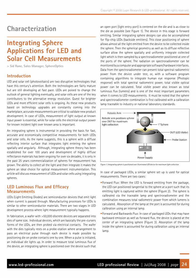
Integrating Sphere Applications for LED and Solar Cell Measurements> Sid Rane, Sales Manager, SphereOptics
Introduction LED and solar cell (photovoltaics) are two disruptive technologies that have this century’s attention. Both the technologies are fairly mature but are still developing at fast pace. LEDs are poised to change the outlook of general lighting eventually, and solar cells are one of the key contributors to the alternative energy revolution. Quest for brighter LEDs and more efficient solar cells is ongoing. As these new products based on technology upgrades are constantly coming into the marketplace, accurate measurements are critical to validate new product development. In case of LEDs, measurement of light output at known input power is essential, while for solar cells the electrical output power for known incident light over known area is important.
An integrating sphere is instrumental in providing the basis for fast, accurate and economically competitive measurements for both LEDs and solar cells. As the name suggests, this is a sphere with a diffuse reflecting interior surface that integrates light entering the sphere spatially and angularly. Although, integrating sphere theory has been established for over 100 years and development of highly diffuse reflectance materials has been ongoing for over six decades, it is only in the past 25 years commercialization of spheres for measurement has grown. The ability to collect all the light and then integrate it makes the sphere an ideal choice for optical measurement instrumentation. This article will discuss measurement of LEDs and solar cells using integrating spheres.
LED Luminous Flux and Efficacy MeasurementsLEDs (Light Emitting Diodes) are semiconductor devices that emit light when current is passed through. Manufacturing processes for LEDs is similar to other semiconductor materials. There are two stages in LED development process where light measurement typically happens.
In fabrication, a wafer with >50,000 discrete devices are separated into dies of same size. Individual devices, which are basically the pre-cursers forms of the LEDs, are then probed via electrical contacts. The wafer with the dies typically rests on a probe-station where arrangement to pass an electrical pulse through each device is made possible by positioning die on probe contacts one by one. When a pulse is initiated, an individual die lights up. In order to measure total luminous flux of the device, an integrating sphere is positioned over the device such that
an open port (light entry port) is centered on the die and is as close to the die as possible (see Figure 1). The device in this stage is forward emitting. Similar integrating sphere designs can also be accomplished for flip-chip LEDs (backside emitters). This close positioning of sphere allows almost all the light emitted from the device to be collected inside the sphere. Then the spherical geometry as well as its diffuse reflective surface allow the sphere spatially and uniformly integrate collected light which is then sampled by a spectroradiometer positioned at one of the ports of the sphere. The radiation on spectroradiometer can be monitored by a computer and appropriate software/hardware interfaces. Data from the spectroradiometer can present total spectral radiometric power from the device under test, or, with a software program containing algorithms to integrate human eye response (Photopic response) with total spectral radiometric power, total visible optical power can be calculated. Total visible power also known as total luminous flux (lumens) and is one of the most important parameters when it comes to LED measurements. It must be noted that the sphere and spectroradiometer combination is first calibrated with a calibration lamp traceable to industry or national laboratory standards.
Figure 1: Integrating sphere is positioned over illuminated LED device for maximum light collection
In case of packaged LEDs, a similar sphere set up is used for optical measurements. There are two cases:
•Forward Flux: When the LED is forward emitting from the package, the LED can positioned tangential to the sphere at a port such that its emitting light is captured within the sphere (Figure 2). The sphere is calibrated via the traceable lamp and spectroradiometer and the combination measures total radiometric power from which lumens is calculated. Absorption of the lamp at the port is accounted for during calibration using an internal lamp.
•Forward and Backwards Flux: In case of packaged LEDs that may have backward emission as well as forward flux, the device is placed at the center of an integrating sphere (Figure 3). Absorption of the lamp inside the sphere is accounted for during calibration using an internal lamp.
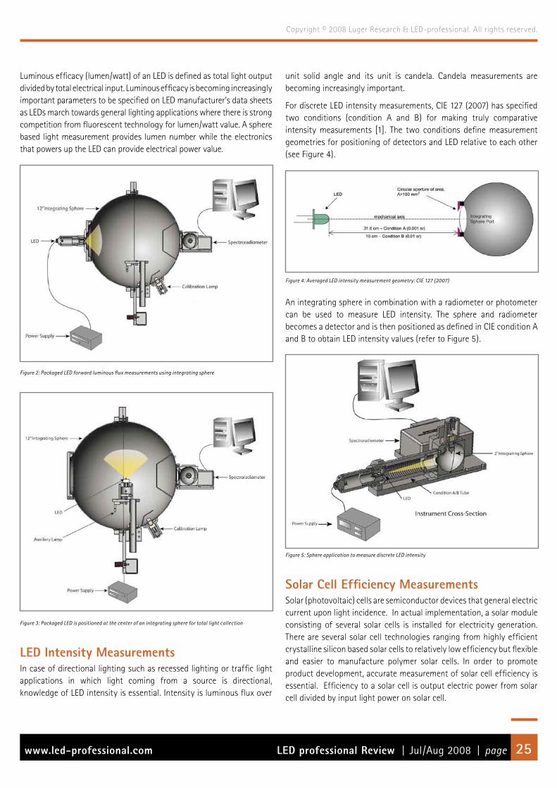
LED professional Review | Jul/Aug 2008 | pagewww.led-professional.com 25
Copyright © 2008 Luger Research & LED-professional. All rights reserved.
Luminous efficacy (lumen/watt) of an LED is defined as total light output divided by total electrical input. Luminous efficacy is becoming increasingly important parameters to be specified on LED manufacturer’s data sheets as LEDs march towards general lighting applications where there is strong competition from fluorescent technology for lumen/watt value. A sphere based light measurement provides lumen number while the electronics that powers up the LED can provide electrical power value.
Figure 2: Packaged LED forward luminous flux measurements using integrating sphere
Figure 3: Packaged LED is positioned at the center of an integrating sphere for total light collection
LED Intensity MeasurementsIn case of directional lighting such as recessed lighting or traffic light applications in which light coming from a source is directional, knowledge of LED intensity is essential. Intensity is luminous flux over
unit solid angle and its unit is candela. Candela measurements are becoming increasingly important.
For discrete LED intensity measurements, CIE 127 (2007) has specified two conditions (condition A and B) for making truly comparative intensity measurements [1]. The two conditions define measurement geometries for positioning of detectors and LED relative to each other (see Figure 4).
Figure 4: Averaged LED intensity measurement geometry: CIE 127 (2007)
An integrating sphere in combination with a radiometer or photometer can be used to measure LED intensity. The sphere and radiometer becomes a detector and is then positioned as defined in CIE condition A and B to obtain LED intensity values (refer to Figure 5).
Figure 5: Sphere application to measure discrete LED intensity
Solar Cell Efficiency MeasurementsSolar (photovoltaic) cells are semiconductor devices that general electric current upon light incidence. In actual implementation, a solar module consisting of several solar cells is installed for electricity generation. There are several solar cell technologies ranging from highly efficient crystalline silicon based solar cells to relatively low efficiency but flexible and easier to manufacture polymer solar cells. In order to promote product development, accurate measurement of solar cell efficiency is essential. Efficiency to a solar cell is output electric power from solar cell divided by input light power on solar cell.

LED professional Review | Jul/Aug 2008 | pagewww.led-professional.com 26
Copyright © 2008 Luger Research & LED-professional. All rights reserved.
Use of an integrating sphere to measure solar cell efficiency is the reverse method as it was for measuring LED light output. In this case, an integrating sphere is used as a light source rather than the collector of light. An integrating sphere is a very good choice as it can offer conditions well suited for solar cell testing. A sphere in combination with multiple light sources can produce a highly uniform illumination source that can either produce near daylight irradiation or spectrally tunable irradiation which is desired for testing of heterojunction solar cells. A device under test (for example a single solar cell) is positioned either on an electrical probe station or attached via electrical leads to an electronics device to register current and voltage. An integrating sphere is then positioned over the solar cell such that solar cell is centered at the sphere port directly above it (see Figure 6). The sphere is illuminated with light sources tuned for desired light level at the exit port or at the surface of solar cell in question. It is to be noted that the solar cell area needs to be overfilled with light incident from the sphere. Also the solar cell needs to be positioned at a distance which allows good irradiance uniformity of light falling on it. An optical system consisting of a fiber conduit or lenses may be required to achieve uniform illumination levels. Given the distance between exit port of sphere and the solar cell, the optical system configuration between the sphere and solar cell, and the wattage of lamps inside sphere, the irradiance (Watts/cm2) at solar cell can be calculated. Upon light incidence, generated electrical power is registered and then knowing the incident power and generated power, solar cell efficiency is obtained.
Figure 6: Integrating sphere is a uniform illumination source for solar cell efficiency measurements
Solar Cell Reflectance MeasurementsReflectance of solar cells also plays a crucial role in solar cell efficiency as it can determine how much light falling on a solar cell actually gets absorbed inside the cell. It is highly desired that solar cells have low reflectance so that most of the light falling on it goes through allowing for higher electron generation.
An integrating sphere can also be used as a device to measure reflectance of solar cells. For this measurement, a typical set up consists of an integrating sphere, a collimated light source, a photodetector with a meter, reflectance standard and solar cell under test (refer to Figure 7). The collimated source is positioned at a sphere port and then a
reflectance standard (or known reflectance sample) is placed at a diametrically-opposed port to the collimated beam. Typically, the standard or sample holder is tilted at 8 degrees so that for mirrored (specular) surfaces reflected light does not go back towards the source but instead is slightly deflected from normal and reflected off the sphere wall and integrated inside the sphere. (An optional optical trap can be added to this set up to exclude specular component of reflected light for measurement.) The diffusely integrated light from the sphere is then measured via a detector-meter combination. The detector is positioned at yet another port typically orthogonal to the sample or standard port. The first set of measurements is done by placing a reflectance standard and measuring the light reflected. This step calibrates the sphere and detector combination for reflectance measurements from the known value of the standard. Secondly, the standard is replaced by solar cell and another measurement is done. Using known reflectance of the standard, reflectance of solar cell in question can be calculated. This method of obtaining solar cell reflectance value is called the substitution method.
Figure 7: Integrating sphere set up for solar cell reflectance testing
There is another preferred method, called comparison method, for measuring reflectance of solar cells. In this method, there is an extra port on the sphere with a sample/standard holder. The holder in light path of collimated source positions a standard and the other holder positions a solar cell under test (not in the collimated beam). A first measurement is taken for these positions of sample and standard. For second measurement, the sample and standard positions are swapped so that now the solar cell under test is in the path of collimated light source. Measurement is taken and ratio of two measurements along with the knowledge of known reflectance of the standard is used to calculate solar cell reflectance. This comparison method eliminates corrective errors known as substitution effects because the sample and the standard are always located on the sphere during measurement.
References
[1] CIE 127: Measurement of LEDs, 2007
LED professional Review | Jul/Aug 2008 | pagewww.led-professional.com 27
Copyright © 2008 Luger Research & LED-professional. All rights reserved.
NIST/DoE: Standards Set for Energy-Conserving LED LightingSolid-state lights are powered by energy-efficient light emitting diodes and are among the first ones of a new generation expected to cut energy needed for lighting by 50 percent by 2027.
Scientists at the National Institute of Standards and Technology (NIST), in cooperation with national standards organizations, have taken the lead in developing the first two standards for solid-state lighting in the United States. This new generation lighting technology uses light-emitting diodes (LEDs) instead of incandescent filaments or fluorescent tubes to produce illumination that cuts energy consumption significantly.
Standards are important to ensure that products will have high quality and their performance will be specified uniformly for commerce and trade. These standards—the most recent of which published last month—detail the color specifications of LED lamps and LED light fixtures, and the test methods that manufacturers should use when testing these solid-state lighting products for total light output, energy consumption and chromaticity, or color quality.
Solid-state lighting is expected to significantly reduce the amount of energy needed for general lighting, including residential, commercial and street lighting. “Lighting,” explains NIST scientist Yoshi Ohno, “uses 22 percent of the electricity and 8 percent of the total energy spent in the country, so the energy savings in lighting will have a huge impact.”
Solid-state lighting is expected to be twice as energy efficient as fluorescent lamps and 10 times more efficient than incandescent lamps, although the current products are still at their early stages. Ohno chaired the task groups that developed these new standards.
In addition to saving energy, the new lighting, if designed appropriately, can produce better color rendering—how colors of objects look under the illumination—than fluorescent lamps or even incandescent lamps, Ohno says.
NIST is working with the U.S. Department of Energy (DOE) to support its goal of developing and introducing solid-state lighting to reduce energy consumption for lighting by 50 percent by the year 2025. The department predicts that phasing in solid-state lighting over the next 20 years could save more than $280 billion in 2007 dollars.
The Illuminating Engineering Society of North America (IESNA) published a documentary standard LM-79, which describes the methods for testing solid-state lighting products for their light output (lumens), energy efficiency (lumens per watt) and chromaticity. Details include the environmental conditions for the tests, how to operate and stabilize the LED sources for testing and methods of measurement and types of instruments to be used.
“More standards are needed, and this will be the foundation for all solid-state lighting standards,” Ohno says. The standard is available from the IESNA.
The solid-state lights being studied are intended for general illumination, but white lights used today vary greatly in chromaticity, or specific shade of white. The American National Standards Institute (ANSI) published the standard C78.377-2008, which specifies the recommended color ranges for solid-state lighting products using cool to warm white LEDs with various correlated color temperatures. The standard may be downloaded from ANSI’s Web site. www.nema.org/stds/ANSI-ANSLG-C78-377.cfm
DOE is launching the Energy Star program for solid-state lighting products this fall. NIST scientists assisted DOE by providing research, technical details and comments for the Energy Star specifications. The Energy Star certification assures consumers that products save energy and are high quality and also serves as an incentive for manufacturers to provide energy-saving products for consumers.
The solid-state lighting community is continuing to develop LED lighting standards for rating LED lamp lifetime and for measuring the performance of the individual high-power LED chips and arrays. NIST scientists are taking active roles in these continuing efforts.
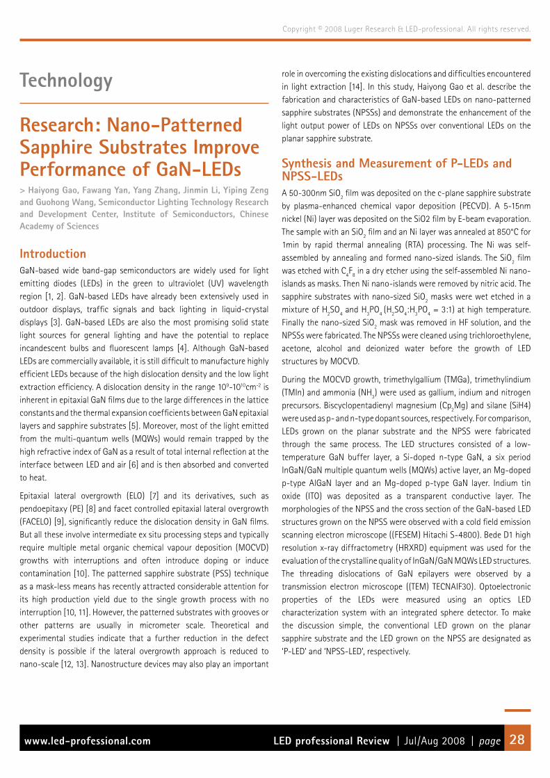
LED professional Review | Jul/Aug 2008 | pagewww.led-professional.com 28
Copyright © 2008 Luger Research & LED-professional. All rights reserved.
Technology
Research: Nano-Patterned Sapphire Substrates Improve Performance of GaN-LEDs> Haiyong Gao, Fawang Yan, Yang Zhang, Jinmin Li, Yiping Zeng and Guohong Wang, Semiconductor Lighting Technology Research and Development Center, Institute of Semiconductors, Chinese Academy of Sciences
IntroductionGaN-based wide band-gap semiconductors are widely used for light emitting diodes (LEDs) in the green to ultraviolet (UV) wavelength region [1, 2]. GaN-based LEDs have already been extensively used in outdoor displays, traffic signals and back lighting in liquid-crystal displays [3]. GaN-based LEDs are also the most promising solid state light sources for general lighting and have the potential to replace incandescent bulbs and fluorescent lamps [4]. Although GaN-based LEDs are commercially available, it is still difficult to manufacture highly efficient LEDs because of the high dislocation density and the low light extraction efficiency. A dislocation density in the range 109-1010cm-2 is inherent in epitaxial GaN films due to the large differences in the lattice constants and the thermal expansion coefficients between GaN epitaxial layers and sapphire substrates [5]. Moreover, most of the light emitted from the multi-quantum wells (MQWs) would remain trapped by the high refractive index of GaN as a result of total internal reflection at the interface between LED and air [6] and is then absorbed and converted to heat.
Epitaxial lateral overgrowth (ELO) [7] and its derivatives, such as pendoepitaxy (PE) [8] and facet controlled epitaxial lateral overgrowth (FACELO) [9], significantly reduce the dislocation density in GaN films. But all these involve intermediate ex situ processing steps and typically require multiple metal organic chemical vapour deposition (MOCVD) growths with interruptions and often introduce doping or induce contamination [10]. The patterned sapphire substrate (PSS) technique as a mask-less means has recently attracted considerable attention for its high production yield due to the single growth process with no interruption [10, 11]. However, the patterned substrates with grooves or other patterns are usually in micrometer scale. Theoretical and experimental studies indicate that a further reduction in the defect density is possible if the lateral overgrowth approach is reduced to nano-scale [12, 13]. Nanostructure devices may also play an important
role in overcoming the existing dislocations and difficulties encountered in light extraction [14]. In this study, Haiyong Gao et al. describe the fabrication and characteristics of GaN-based LEDs on nano-patterned sapphire substrates (NPSSs) and demonstrate the enhancement of the light output power of LEDs on NPSSs over conventional LEDs on the planar sapphire substrate.
Synthesis and Measurement of P-LEDs and NPSS-LEDsA 50-300nm SiO2 film was deposited on the c-plane sapphire substrate by plasma-enhanced chemical vapor deposition (PECVD). A 5-15nm nickel (Ni) layer was deposited on the SiO2 film by E-beam evaporation. The sample with an SiO2 film and an Ni layer was annealed at 850°C for 1min by rapid thermal annealing (RTA) processing. The Ni was self-assembled by annealing and formed nano-sized islands. The SiO2 film was etched with C4F8 in a dry etcher using the self-assembled Ni nano-islands as masks. Then Ni nano-islands were removed by nitric acid. The sapphire substrates with nano-sized SiO2 masks were wet etched in a mixture of H2SO4 and H3PO4 (H2SO4:H3PO4 = 3:1) at high temperature. Finally the nano-sized SiO2 mask was removed in HF solution, and the NPSSs were fabricated. The NPSSs were cleaned using trichloroethylene, acetone, alcohol and deionized water before the growth of LED structures by MOCVD.
During the MOCVD growth, trimethylgallium (TMGa), trimethylindium (TMIn) and ammonia (NH3) were used as gallium, indium and nitrogen precursors. Biscyclopentadienyl magnesium (Cp2Mg) and silane (SiH4) were used as p- and n-type dopant sources, respectively. For comparison, LEDs grown on the planar substrate and the NPSS were fabricated through the same process. The LED structures consisted of a low-temperature GaN buffer layer, a Si-doped n-type GaN, a six period InGaN/GaN multiple quantum wells (MQWs) active layer, an Mg-doped p-type AlGaN layer and an Mg-doped p-type GaN layer. Indium tin oxide (ITO) was deposited as a transparent conductive layer. The morphologies of the NPSS and the cross section of the GaN-based LED structures grown on the NPSS were observed with a cold field emission scanning electron microscope ((FESEM) Hitachi S-4800). Bede D1 high resolution x-ray diffractometry (HRXRD) equipment was used for the evaluation of the crystalline quality of InGaN/GaN MQWs LED structures. The threading dislocations of GaN epilayers were observed by a transmission electron microscope ((TEM) TECNAIF30). Optoelectronic properties of the LEDs were measured using an optics LED characterization system with an integrated sphere detector. To make the discussion simple, the conventional LED grown on the planar sapphire substrate and the LED grown on the NPSS are designated as ‘P-LED’ and ‘NPSS-LED’, respectively.

LED professional Review | Jul/Aug 2008 | pagewww.led-professional.com 29
Copyright © 2008 Luger Research & LED-professional. All rights reserved.
LED Efficacy: A Matter of Die Structures> A comment by Arno Grabher-Meyer, LED professional
Two main mechanisms are crucial for SSL efficacy. First, the quality of the epitaxy layer which determines the internal quantum efficiency. Second, the optical properties - like refractive index, die geometry and surface structures – which determine the light-extraction efficiency. While the internal quantum efficiency - up to 75% - is still at a relatively high level, today’s even best high brightness LEDs already suffer from low light-extraction efficiency - between 20 and 50%. As a result, of these parameters, overall efficacy of recent high power LEDs is limited to about 100lm/W, out of the theoretical limit of 300 to 400lm/W.
All LED manufacturers have undertaken great endeavors to optimize light extraction to attain today’s values. Very different approaches can be recognized, some of these are published, others are protected by patents or pending patents and some are trade secrets.
A chip-geometry similar to the frustum of a pyramid is still in mass production - a relative simple, hence rea-sonable, but effective improvement, as a result of technological evolution
A solution with a rough, corrugated surface to enhance randomization of photon scattering was introduced by another manufacturer recently
In different research laboratories, new structures and production methods with excellent properties have been developed and tested in recent years, applied to a handful of lab samples. Most of these methods have the same disadvantages: They often require complex manufacturing methods with low yields, and therefore they are very costly and potentially will stay expensive in the near future. Hence a relatively simple-to-apply and cost-effective method would be a big step forward for LED businesses.
For instance, photonic crystals are promoted as a promising solution with a 50% increase of efficiency. Small holes are introduced into LED dies, for example 200 nanometers (nm) in diameter, 400 times narrower than a human hair but only penetrating 100nm into the LED’s surface, and spaced 300nm apart. Researchers stated, “Fabrication of photonic crystals in GaN is complicated by the difficulty of etching the material, which is extremely hard and chemically inert.“
Different production methods were suggested, e.g. a team of researchers from the University of Glasgow un-der the lead of Dr. Faiz Rahman used nano-imprint lithography
The photonic-crystal LEDs strongly modified far-field pattern shows a triangular symmetry due to the extrac-tion of waveguided modes and showed a 50% increase in efficiency compared to the controls
Most solutions focus on structuring the upper, light emitting surface. Another approach is the treatment of the substrate and, in this way, the structuring of the reflection area. Following this idea, the authors of the article “Nano-Patterned Sapphire Substrates Improve Performance of GaN-LEDs”, Haiyong Gao, Fawang Yan, Yang Zhang, Jinmin Li, Yiping Zeng and Guohong Wang, claim a cost-effective and relatively simple production of the device, while showing remarkably enhanced performance.
Many approaches sound very promising, but we should keep in mind, these results come out of a lab: Could it be possible that the reference performs poorly? What kind of LED is it: Low, mid or high power LED? Could a solution have disadvantages on another scale, e.g. for high power LEDs? Does the technology fit a manufacturer’s production method, because they have to take additional design properties into account?
Besides these questions many other things have to be answered before implementing in a process for mass production process. All in all, it is just a matter of time when one of these research results will create a new standard.
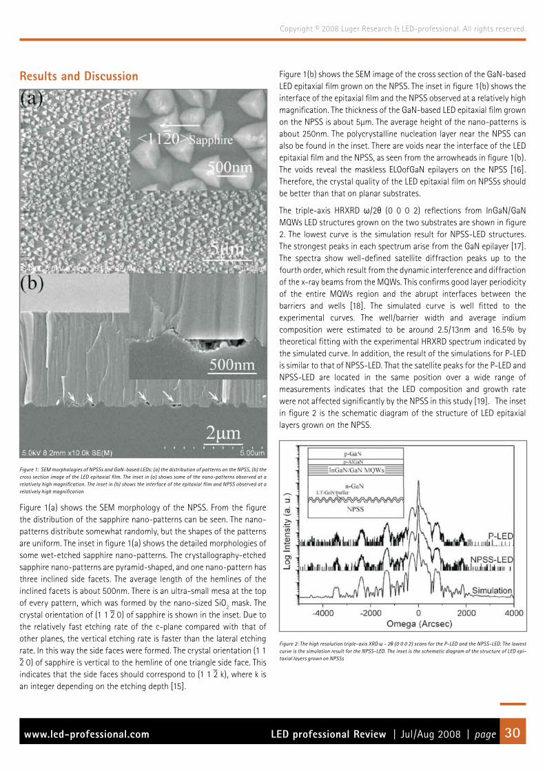
LED professional Review | Jul/Aug 2008 | pagewww.led-professional.com 30
Copyright © 2008 Luger Research & LED-professional. All rights reserved.
Results and Discussion
Figure 1: SEM morphologies of NPSSs and GaN-based LEDs: (a) the distribution of patterns on the NPSS, (b) the cross section image of the LED epitaxial film. The inset in (a) shows some of the nano-patterns observed at a relatively high magnification. The inset in (b) shows the interface of the epitaxial film and NPSS observed at a relatively high magnification
Figure 1(a) shows the SEM morphology of the NPSS. From the figure the distribution of the sapphire nano-patterns can be seen. The nano-patterns distribute somewhat randomly, but the shapes of the patterns are uniform. The inset in figure 1(a) shows the detailed morphologies of some wet-etched sapphire nano-patterns. The crystallography-etched sapphire nano-patterns are pyramid-shaped, and one nano-pattern has three inclined side facets. The average length of the hemlines of the inclined facets is about 500nm. There is an ultra-small mesa at the top of every pattern, which was formed by the nano-sized SiO2 mask. The crystal orientation of (1 1 2 0) of sapphire is shown in the inset. Due to the relatively fast etching rate of the c-plane compared with that of other planes, the vertical etching rate is faster than the lateral etching rate. In this way the side faces were formed. The crystal orientation (1 1 2 0) of sapphire is vertical to the hemline of one triangle side face. This indicates that the side faces should correspond to (1 1 2 k), where k is an integer depending on the etching depth [15].
Figure 1(b) shows the SEM image of the cross section of the GaN-based LED epitaxial film grown on the NPSS. The inset in figure 1(b) shows the interface of the epitaxial film and the NPSS observed at a relatively high magnification. The thickness of the GaN-based LED epitaxial film grown on the NPSS is about 5µm. The average height of the nano-patterns is about 250nm. The polycrystalline nucleation layer near the NPSS can also be found in the inset. There are voids near the interface of the LED epitaxial film and the NPSS, as seen from the arrowheads in figure 1(b). The voids reveal the maskless ELOofGaN epilayers on the NPSS [16]. Therefore, the crystal quality of the LED epitaxial film on NPSSs should be better than that on planar substrates.
The triple-axis HRXRD ω/2θ (0 0 0 2) reflections from InGaN/GaN MQWs LED structures grown on the two substrates are shown in figure 2. The lowest curve is the simulation result for NPSS-LED structures. The strongest peaks in each spectrum arise from the GaN epilayer [17]. The spectra show well-defined satellite diffraction peaks up to the fourth order, which result from the dynamic interference and diffraction of the x-ray beams from the MQWs. This confirms good layer periodicity of the entire MQWs region and the abrupt interfaces between the barriers and wells [18]. The simulated curve is well fitted to the experimental curves. The well/barrier width and average indium composition were estimated to be around 2.5/13nm and 16.5% by theoretical fitting with the experimental HRXRD spectrum indicated by the simulated curve. In addition, the result of the simulations for P-LED is similar to that of NPSS-LED. That the satellite peaks for the P-LED and NPSS-LED are located in the same position over a wide range of measurements indicates that the LED composition and growth rate were not affected significantly by the NPSS in this study [19]. The inset in figure 2 is the schematic diagram of the structure of LED epitaxial layers grown on the NPSS.
Figure 2: The high resolution triple-axis XRD ω - 2θ (0 0 0 2) scans for the P-LED and the NPSS-LED. The lowest curve is the simulation result for the NPSS-LED. The inset is the schematic diagram of the structure of LED epi-taxial layers grown on NPSSs

LED professional Review | Jul/Aug 2008 | pagewww.led-professional.com 31
Copyright © 2008 Luger Research & LED-professional. All rights reserved.
Figure 3 shows the cross-sectional TEM images of GaN grown on the planar substrate (a), (c) and the NPSS (b), (d). Figures 3(a) and (b) correspond to g = [0002]. Figures 3(c) and (d) correspond to g = [1100]. The nano-patterns of NPSS in figures 3(b) and (d) are marked by arrowheads. As seen from figures 3(a) and (c), there are many threading dislocations which are vertical to the substrates. The threading dislocation density of GaN grown on the planar substrate is estimated to be about 1 x 109cm-2. While for the GaN grown on the NPSS, the quantity of the threading dislocations is very little. The threading dislocation density of GaN grown on the NPSS is estimated to be less than 1 x 107cm-2. This indicates that the nano-patterns help in relaxing the stress in the GaN epilayers and improving the crystal quality.
Figure3: Cross-sectional TEM images of GaN grown on planar substrate (a), (c) and NPSS (b), (d) with g = [0 0 0 2] (a), (b) and g = [1 1 0 0] (c), (d)
Figure 4 shows the normalized EL spectra under an injection current from 5 to 100mA for P-LED (a) and NPSS-LED (b). As seen from the dashed line, the EL peak positions of both the blue spectrum shifts first and then red spectrum shifts. When the injection current increases from 5 to 100mA, the EL emission peak wavelengths of P-LED blue- shift from 458 to 454nm first and then red-shift to 462nm. For NPSS-LED the blue shifts from 456 to 452nm first and then to 460nm. The blue-shift is due to the band filling effect and the screening effect in a piezoelectric field quantum well [20, 21]. The band filling effect is due to carriers becoming excited and moving to higher energy states at higher injection currents. The screening effect is due to the piezoelectric field affecting the optical properties of the InGaN active layer. The red-shift can be explained by the effect of band shrinkage due to Joule heat generation [21]. The peak wavelength of P-LED is longer than that of NPSS-LED in the case of the same injection current, as seen from the figure. The compressive strain will be induced when GaN is grown on
the planar sapphire due to the large lattice mismatch. The compressive strain can induce piezoelectric polarization and result in the quantum confined Stark effect. The quantum confined Stark effect will bring about the red-shift of optical transitions [22]. So the red-shift of EL spectroscopy of P-LED compared with NPSS-LED may indicate a relief in compressive stress in the GaN epilayer when grown on the NPSS.
Figure 4: The normalized EL spectra in relation to the injection current for the P-LED (a) and the NPSS-LED (b)
Figure 5 shows the light output powers and forward voltages in relation to the injection currents (L-I-V) characteristics for the two LEDs. The output power of the NPSS-LED is larger than that of the P-LED at every corresponding injection current. At a 20mA forward injection current, the light output power of P-LED and NPSS-LED was 9.28mW and 13.78mW, respectively. Therefore, an enhancement in the output power of about 48% is achieved when NPSSs are used, respectively. Furthermore, the output intensities of the two LEDs increase as the forward injection current increases, until reaching the maximum at 85mA for P-LED (21.67mW) and 90mA for NPSS-LED (37.8mW). Then the output intensities decrease as the injection current further increases. The decrease in output power is attributed to the thermal dissipation problem, which occurs at high current injection [23]. Non-radiative recombination occurring in dislocation will result in heat generation. The thermal effect at higher temperatures causes an increase in the nonradiative recombination rate in the LEDs. The energized carriers that gain more thermal energy easily escape from the heterojunction confinement in the InGaN/GaN MQW active layer [24]. Therefore, the

LED professional Review | Jul/Aug 2008 | pagewww.led-professional.com 32
Copyright © 2008 Luger Research & LED-professional. All rights reserved.
radiative recombination rate was aggravated by the thermal effect at higher temperatures. The dislocation density in LEDs grown on NPSS is smaller; thus, the thermal dissipation problem will be less severe. For I-V curves, the turn-on voltages of the two LEDs are both about 2.8 V. As seen from the curves, the forward voltages of NPSS are smaller than that of P-LED in the case of the same injection current. The forward voltages of 3.28 V and 3.23 V were measured at the injection current of 20mA for P-LED and NPSS-LED, respectively. This indicates that LEDs have a better electronic property when grown on NPSSs. The reason may be that the GaN epilayers grown on NPSSs have a better crystal quality.
Figure 5: Room-temperature L-I-V characteristics of the P-LED (squares) and the NPSS-LED (triangles)
Figure 6 gives a schematic ray-tracing of light for P-LEDs (solid) and NPSS-LEDs (dashed). GaN has a high index of refraction (n = 2.5), while air has a low index of refraction (n = 1.0). According to Snell’s law, light that is only within a critical angle of 23° can cross the air when traveling from a GaN surface to air [25]. Even though an ITO layer (n = 1.9) is deposited on p-type GaN, the problem of light extraction still exists. So the key to enhancing the escape probability is to give the photons multiple opportunities to find the escape cone. As seen from figure 6, In the case of the P-LED, the light rays a0 and b0 emitting from the MQWs with incidence beyond the critical angle will not cross the air but experience total internal reflection (as seen from the light rays a1 and b1) that continues to be reflected within the LED until they are absorbed and converted to heat, while for the patterned substrates, the inclined planes of the patterns can redirect the photons back into the escape cone on the top of the device surfaces, as seen from the light rays a2 and b2. At the same time, the nano-patterns can redirect the photons that experience total reflection such as a1 and b1 to find their escape cones. On the other hand, the nano-patterns can also benefit the emission of light from the sapphire side which will be reflected by the reflector cup, as seen from the light ray b3. All these indicate that the probability of photons escaping from the LED surface increases, resulting in an enhancement of light extraction efficiency. So the significant enhancement of light output powers should be attributed to the improvement in the crystal quality of GaN-based epilayers and the improvement in the light extraction efficiency due to the NPSS.
Figure 6: A schematic ray-tracing of light for the P-LEDs (solid) and NPSS-LEDs (dashed)
ConclusionsIn conclusion, the fabrication and application of NPSSs was presented, and the characteristics were compared with GaN-based LEDs, grown on the planar sapphire substrate. The LEDs grown on NPSSs exhibit improved optoelectronic characteristics, namely improvement in the light extraction efficiency. This study presents a simple and effective technology for the reduction of the dislocation density of GaN and the significant improvement in the performance of GaN-based LEDs.
Acknowledgment
This work was supported by the National ‘863’ Project of China (Grant No 006AA03A102)and is republished from Journal of Physics. D: Appl. Phys. 41 (2008) 115106 (5pp)
References
[1] Oh M S, Kwon M K, Park I K, Baek S H, Park S J, Lee S H and Jung J J 2006 J. Cryst. Growth 289 107[2] Morita D, Yamamoto M, Akaishi K, Matoba K, Yasutomo K, Kasai Y, Sano M, Nagahama S and Mukai T 2004 Japan. J. Appl. Phys. 43 5945[3] Chang S J, Lin Y C, Su Y K, Chang C S, Wen T C, Shei S C, Ke J C, Kuo C W, Chen S C and Liu C H 2003 Solid-State Electron. 47 1539 [4] Narukawa Y, Narita J, Sakamoto T, Deguchi K, Yamada T and Muka T 2006 Japan. J. Appl. Phys. 45 L1084 [5] Feng Z H, Qi Y D, Lu Z D and Lau K M 2004 J. Cryst. Growth 272 327 [6] Cuong T V, Cheong H S, Kim H G, Kim H Y, Hong C H, Suh E K, Cho H K and Kong B H 2007 Appl. Phys. Lett. 90 131107 [7] Gradeeak S, Stadelmann P, Wagner V and Ilegems M 2004 Appl. Phys. Lett. 85 4648 [8] Einfeldt S, Roskowski A M, Preble E A and Davis R F 2002 Appl. Phys. Lett. 80 953 [9] Hiramatsu K, Nishiyama K, Onishi M, Mizutani H, Narukawa M, Motogaito A, Miyake H, Iyechika Y and Maeda T 2000 J. Cryst. Growth 221 316 [10] Horng R H, Wang W K, Huang S C, Huang S Y Lin S H, Lin C F and Wuu D S 2007 J. Cryst. Growth 298 219 [11] Lee Y J et al 2005 Mater. Sci. Eng. B 122 184 [12] Hersee S D, Zubia D, Sun X, Bommena R, Fairchild M, Zhang S, Burckel D, Frauenglass A and Brueck S R J 2002 IEEEJ. Quantum Electron. 38 1017 [13] Zang K Y Wang Y D, Chua S J and Wang L S 2005 Appl. Phys. Lett. 87 193106 [14] Ko T S, Wang T C, Gao R C, Lee Y J, Lu T C, Kuo H C, Wang S C and Chen H G 2007 Appl. Phys. Lett. 90 013110 [15] Wuu D S, Wang W K, Wen K S, Huang S C, Lin S H, Horng R H, Yu Y S and Pan M H 2006 J. Electrochem. Soc. 153 G765 [16] Barabash R I, Roder C, Ice G E, Einfeldt S, Budai J D, Barabash O M, Figge S and Hommel D 2006 J. Appl. Phys. 100 053103 [17] Chen C H, Chang S J, Su Y K, Chi G C, Sheu J K and Chen J F 2002 IEEEJ. Sel. Top. Quantum Electron. 8 284 [18] Cheonga M G, Suh E K and Lee H J 2002 J. Lumin. 99 265 [19] Lee Y J, Kuo H C, Lu T C, Su B J and Wang S C 2006 J. Electrochem. Soc. 153 G1106 [20] Zhang B, Egawa T, Ishikawa H, Liu Y and Jimbo T 2004 J. Appl. Phys. 95 3170 [21] Huang H W, Lai C F, Wang W C, Lu T C, Kuo H C, Wang S C, Tsai R J and Yu C C 2007 Electrochem. Solid-State Lett. 10H59 [22] Chakraborty A, Keller S, Meier C, Haskell B A, Keller S, Waltereit P, DenBaars S P, Nakamura S, Speck J S and Mishra U K 2005 Appl. Phys. Lett. 86 031901 [23] Wuu D S, Wang W K, Wen K S, Huang S C, Lin S H, Huang S Y Lin C F and Horng R H 2006 Appl. Phys. Lett. 89 161105 [24] Lee H Y Pan K H, Lin C C, Chang Y C, Kao F J and Lee C T 2007 J. Vac. Sci. Technol. B 25 1280
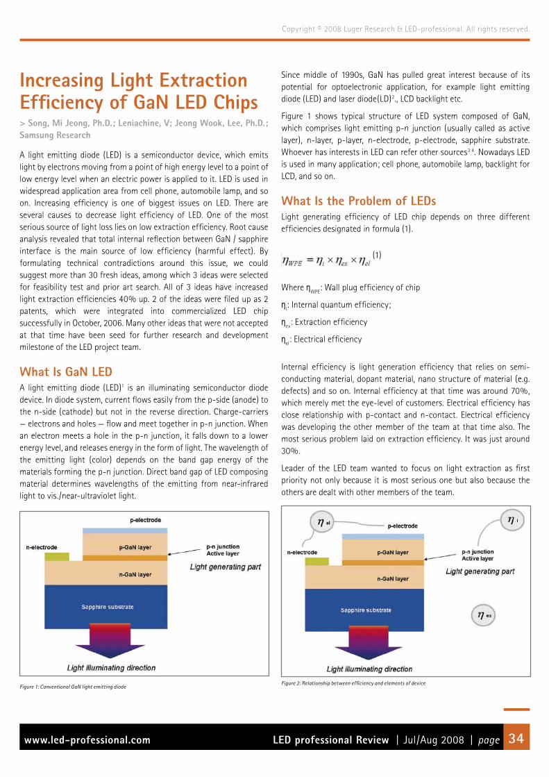
LED professional Review | Jul/Aug 2008 | pagewww.led-professional.com 34
Copyright © 2008 Luger Research & LED-professional. All rights reserved.
Since middle of 1990s, GaN has pulled great interest because of its potential for optoelectronic application, for example light emitting diode (LED) and laser diode(LD)2., LCD backlight etc.
Figure 1 shows typical structure of LED system composed of GaN, which comprises light emitting p-n junction (usually called as active layer), n-layer, p-layer, n-electrode, p-electrode, sapphire substrate. Whoever has interests in LED can refer other sources3 4. Nowadays LED is used in many application; cell phone, automobile lamp, backlight for LCD, and so on.
What Is the Problem of LEDsLight generating efficiency of LED chip depends on three different efficiencies designated in formula (1).
(1)
Where ηWPE: Wall plug efficiency of chip
ηi: Internal quantum efficiency;
ηex: Extraction efficiency
ηel: Electrical efficiency
Internal efficiency is light generation efficiency that relies on semi-conducting material, dopant material, nano structure of material (e.g. defects) and so on. Internal efficiency at that time was around 70%, which merely met the eye-level of customers. Electrical efficiency has close relationship with p-contact and n-contact. Electrical efficiency was developing the other member of the team at that time also. The most serious problem laid on extraction efficiency. It was just around 30%.
Leader of the LED team wanted to focus on light extraction as first priority not only because it is most serious one but also because the others are dealt with other members of the team.
Figure 2: Relationship between efficiency and elements of device
Increasing Light Extraction Efficiency of GaN LED Chips> Song, Mi Jeong, Ph.D.; Leniachine, V; Jeong Wook, Lee, Ph.D.; Samsung Research
A light emitting diode (LED) is a semiconductor device, which emits light by electrons moving from a point of high energy level to a point of low energy level when an electric power is applied to it. LED is used in widespread application area from cell phone, automobile lamp, and so on. Increasing efficiency is one of biggest issues on LED. There are several causes to decrease light efficiency of LED. One of the most serious source of light loss lies on low extraction efficiency. Root cause analysis revealed that total internal reflection between GaN / sapphire interface is the main source of low efficiency (harmful effect). By formulating technical contradictions around this issue, we could suggest more than 30 fresh ideas, among which 3 ideas were selected for feasibility test and prior art search. All of 3 ideas have increased light extraction efficiencies 40% up. 2 of the ideas were filed up as 2 patents, which were integrated into commercialized LED chip successfully in October, 2006. Many other ideas that were not accepted at that time have been seed for further research and development milestone of the LED project team.
What Is GaN LEDA light emitting diode (LED)1 is an illuminating semiconductor diode device. In diode system, current flows easily from the p-side (anode) to the n-side (cathode) but not in the reverse direction. Charge-carriers — electrons and holes — flow and meet together in p-n junction. When an electron meets a hole in the p-n junction, it falls down to a lower energy level, and releases energy in the form of light. The wavelength of the emitting light (color) depends on the band gap energy of the materials forming the p-n junction. Direct band gap of LED composing material determines wavelengths of the emitting from near-infrared light to vis./near-ultraviolet light.
Figure 1: Conventional GaN light emitting diode
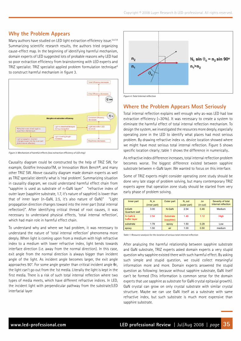
LED professional Review | Jul/Aug 2008 | pagewww.led-professional.com 35
Copyright © 2008 Luger Research & LED-professional. All rights reserved.
Why the Problem AppearsMany authors have studied on LED light extraction efficiency issue.5,6,7,8 Summarizing scientific research results, the authors tried organizing cause-effect map. In the beginning of identifying harmful mechanism, domain experts of LED suggested lots of probable reasons why LED had so poor extraction efficiency from brainstorming with LED experts and TRIZ specialist. TRIZ specialist applied problem formulation technique9 to construct harmful mechanism in figure 3.
Figure 3: Mechanism of harmful effects (low extraction efficiency of LED chip)
Causality diagram could be constructed by the help of TRIZ SW, for example, Goldfire InnovatorTM, or Innovation Work Bench®, and many other TRIZ SW. Above causality diagram made domain experts as well as TRIZ specialist identify what is ‘real problem’. Summarizing situation in causality diagram, we could understand harmful effect chain from “sapphire is used as substrate of n-GaN layer” € “refractive index of outer layer (sapphire substrate, 1.7, it’s nature of sapphire) is lower than that of inner layer (n-GaN, 2.5, it’s also nature of GaN)” € “Light propagation direction changes toward into the inner part (total internal reflection)”. After identifying critical thread of root causes, it was necessary to understand physical effects, ‘total internal reflection’, which had main role in harmful effect chain.
To understand why and where we had problem, it was necessary to understand the nature of ‘total internal reflection’ phenomena more deeply. When light is coming upon from a medium with high refractive index to a medium with lower refractive index, light bends towards interface direction (i.e. away from the normal direction). In this case, exit angle from the normal direction is always bigger than incident angle of the light. As incident angle becomes larger, the exit angle approaches 90°. For some angle greater than critical incident angle θc, the light can’t go out from the 1st media. Literally the light is kept in the first media. There is a risk of such total internal reflection where two types of media meets, which have different refractive indices. In LED, the incident light with perpendicular pathway from the substrate/LED interfacial layer
Figure 4: Total Internal reflection
Where the Problem Appears Most SeriouslyTotal internal reflection explains well enough why as-was LED had low extraction efficiency (~30%). It was necessary to create a system to eliminate the harmful effect of total internal reflection mechanism. To design the system, we investigated the resources more deeply, especially operating zone in the LED to identify what places had most serious problem. By drawing refractive index vs. device location showed where we might have most serious total internal reflection. Figure 5 shows specific location clearly; table 1 shows the difference in numerically..
As refractive index difference increases, total internal reflection problem becomes worse. The biggest difference existed between sapphire substrate between n-GaN layer. We wanted to focus on this interface.
Some of TRIZ experts might consider operating zone study should be done very late stage of problem solving, but many contemporary TRIZ experts agree that operation zone study should be started from very early phase of problem solving.
mediumLow
High
Medium
Severity of total internal reflection
0.501.00air1.50epoxy0.281.50epoxy1.78substrate
1.121.46Substrate(sapphire)
2.54N-GaN & buffer layer
0.462.54N-GaN3.00InGaN Quantum well
∆n(in-out)
N_out(outer part)
Outer partN_in(inner part)
Inner part
mediumLow
High
Medium
Severity of total internal reflection
0.501.00air1.50epoxy0.281.50epoxy1.78substrate
1.121.46Substrate(sapphire)
2.54N-GaN & buffer layer
0.462.54N-GaN3.00InGaN Quantum well
∆n(in-out)
N_out(outer part)
Outer partN_in(inner part)
Inner part
Table 1: Resource analysis for the location of serious total internal reflection
After analyzing the harmful relationship between sapphire substrate and GaN substrate, TRIZ experts asked domain experts a very stupid question why sapphire existed there with such harmful effect. By asking such simple and stupid question, we could collect meaningful information more and more. Domain experts answered the stupid question as following: because without sapphire substrate, GaN itself can’t be formed (This information is common sense for the domain experts that use sapphire as substrate for GaN crystal epitaxial growth). GaN crystal can grow on only crystal substrate with similar crystal structure. Maybe we can use GaN itself as a substrate with same refractive index, but such substrate is much more expensive than sapphire substrate.
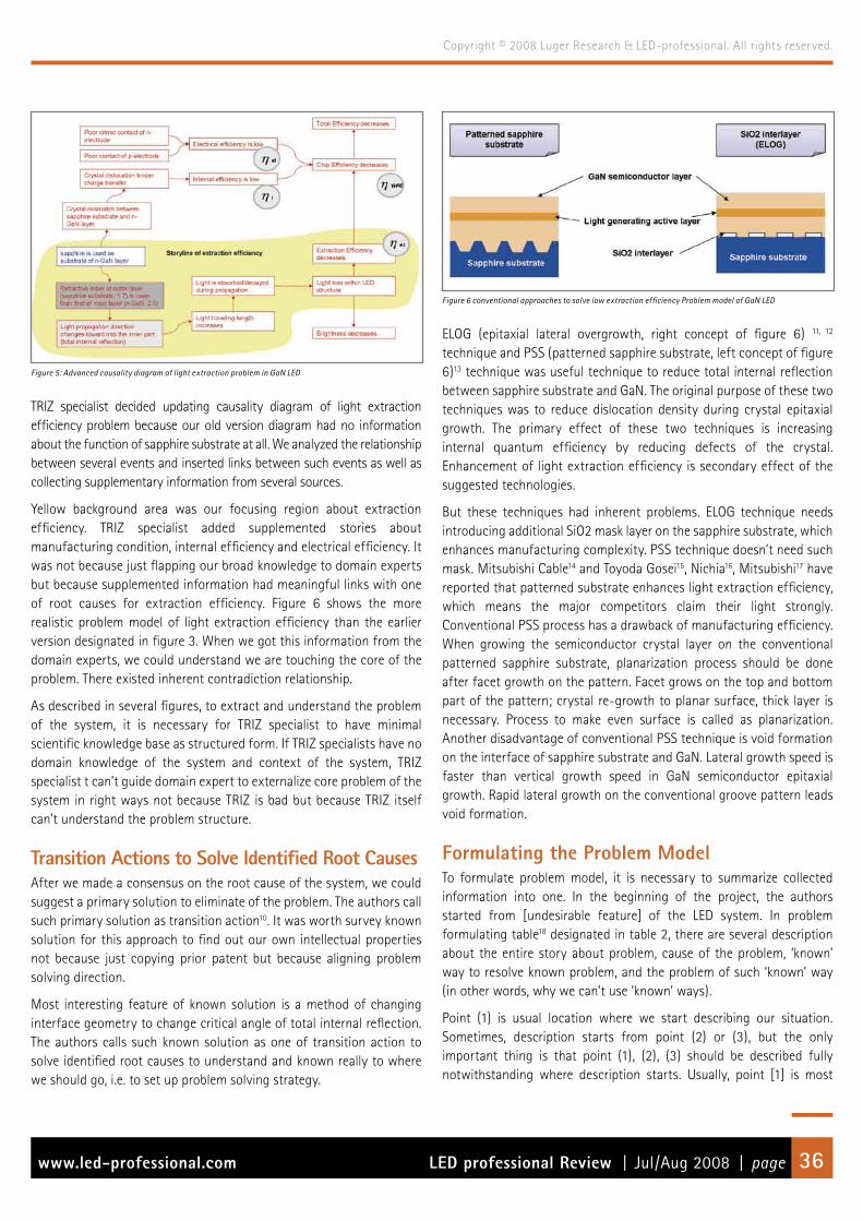
LED professional Review | Jul/Aug 2008 | pagewww.led-professional.com 36
Copyright © 2008 Luger Research & LED-professional. All rights reserved.
Figure 5: Advanced causality diagram of light extraction problem in GaN LED
TRIZ specialist decided updating causality diagram of light extraction efficiency problem because our old version diagram had no information about the function of sapphire substrate at all. We analyzed the relationship between several events and inserted links between such events as well as collecting supplementary information from several sources.
Yellow background area was our focusing region about extraction efficiency. TRIZ specialist added supplemented stories about manufacturing condition, internal efficiency and electrical efficiency. It was not because just flapping our broad knowledge to domain experts but because supplemented information had meaningful links with one of root causes for extraction efficiency. Figure 6 shows the more realistic problem model of light extraction efficiency than the earlier version designated in figure 3. When we got this information from the domain experts, we could understand we are touching the core of the problem. There existed inherent contradiction relationship.
As described in several figures, to extract and understand the problem of the system, it is necessary for TRIZ specialist to have minimal scientific knowledge base as structured form. If TRIZ specialists have no domain knowledge of the system and context of the system, TRIZ specialist t can’t guide domain expert to externalize core problem of the system in right ways not because TRIZ is bad but because TRIZ itself can’t understand the problem structure.
Transition Actions to Solve Identified Root CausesAfter we made a consensus on the root cause of the system, we could suggest a primary solution to eliminate of the problem. The authors call such primary solution as transition action10. It was worth survey known solution for this approach to find out our own intellectual properties not because just copying prior patent but because aligning problem solving direction.
Most interesting feature of known solution is a method of changing interface geometry to change critical angle of total internal reflection. The authors calls such known solution as one of transition action to solve identified root causes to understand and known really to where we should go, i.e. to set up problem solving strategy.
Figure 6 conventional approaches to solve low extraction efficiency Problem model of GaN LED
ELOG (epitaxial lateral overgrowth, right concept of figure 6) 11, 12 technique and PSS (patterned sapphire substrate, left concept of figure 6)13 technique was useful technique to reduce total internal reflection between sapphire substrate and GaN. The original purpose of these two techniques was to reduce dislocation density during crystal epitaxial growth. The primary effect of these two techniques is increasing internal quantum efficiency by reducing defects of the crystal. Enhancement of light extraction efficiency is secondary effect of the suggested technologies.
But these techniques had inherent problems. ELOG technique needs introducing additional SiO2 mask layer on the sapphire substrate, which enhances manufacturing complexity. PSS technique doesn’t need such mask. Mitsubishi Cable14 and Toyoda Gosei15, Nichia16, Mitsubishi17 have reported that patterned substrate enhances light extraction efficiency, which means the major competitors claim their light strongly. Conventional PSS process has a drawback of manufacturing efficiency. When growing the semiconductor crystal layer on the conventional patterned sapphire substrate, planarization process should be done after facet growth on the pattern. Facet grows on the top and bottom part of the pattern; crystal re-growth to planar surface, thick layer is necessary. Process to make even surface is called as planarization. Another disadvantage of conventional PSS technique is void formation on the interface of sapphire substrate and GaN. Lateral growth speed is faster than vertical growth speed in GaN semiconductor epitaxial growth. Rapid lateral growth on the conventional groove pattern leads void formation.
Formulating the Problem ModelTo formulate problem model, it is necessary to summarize collected information into one. In the beginning of the project, the authors started from [undesirable feature] of the LED system. In problem formulating table18 designated in table 2, there are several description about the entire story about problem, cause of the problem, ‘known’ way to resolve known problem, and the problem of such ‘known’ way (in other words, why we can’t use ‘known’ ways).
Point (1) is usual location where we start describing our situation. Sometimes, description starts from point (2) or (3), but the only important thing is that point (1), (2), (3) should be described fully notwithstanding where description starts. Usually, point [1] is most

LED professional Review | Jul/Aug 2008 | pagewww.led-professional.com 37
Copyright © 2008 Luger Research & LED-professional. All rights reserved.
easily identifiable part in system/problem complex. The authors defines it ‘passive knowledge’ that undesirable function (point (1)), the reason to eliminate undesirable function (point (2)), the cause of undesirable function (point (3)). Point 4 is starting point of so called active analysis. The authors started to survey ‘transition action’ to make up over the identified undesirable feature of its origin. The authors analyzed drawbacks of such transition actions and/or why we could use known transition action to eliminate undesirable function in detail denoted in point (5). Table 2 summarizes the logic of TRIZ-like problem formulation from real situation. Table 2 provides a template for problem model formulation also.
Table 2: Problem formulating table: substrate modification
Technical contradiction could be defined at any hierarchy in system/problem complex denoted in root cause analysis diagram. For the purpose of product design upgrade, competitor’s solution for the same problem is a most pragmatic starting point of contradiction resolving journey. We can set competitor’s solution as one of transition action for our problem.
We defined our pragmatic contradiction as following.
•TC1-0: If SiO2 mask is introduced on the sapphire substrate(ELOG technique), total internal reflection is reduced(good), but additional mask generates manufacturing complexity(bad)
• TC1-1.If SiO2 mask is absent (conventional even structure), manufacturing complexity is minimized (good), but total internal reflection exists(bad).
• TC2-0: If groove pattern is introduced on the sapphire substrate(PSS technique), total internal reflection is reduced(good), but manufacturing process is slow(bad1) and void appears on the interface(bad2)
• TC2-1. If groove pattern is absent (conventional even structure), manufacturing complexity is minimized (good), but total internal reflection exists (bad).
According to the domain experts, introducing mask during manufacturing process is very complex, which increases cost of the device. An attempt to direction no.1 is more difficult to solve than direction 2. The authors decided to follow the second direction, i.e.
groove introduction. We referred to contradiction matrix and picked up some meaningful inventive principles as following. We chose TC2-0 as main direction of solving, because efficiency enhancing met the requirement of customers.
• Contradiction using natural language: introduction groove to reduce total internal reflection (good) ↔ manufacturing process time(bad), unwanted void on the interface (bad)
• Contradiction using 39 parameters: shape ↔ object generated harmful factors, shape ↔ object affected harmful factors
Worsening feature
Improving feature
Object generated harmful factors
Object affected harmful factors
shape 35. Parameter change
01. Segmentation
22. Blessing in disguise
01. Segmentation
02. Separation
35. Parameter change
Among recommended principles, no.35 parameter changes seemed most promising direction for further ideation. Controllable parameters in our system could be listed as following. This description comes from simple resource analysis of the system.
•Parameter of incident light itself o Angle toward the interfaceo Propagation trajectoryo Wavelengtho Wavelength distributiono Polarization, etc.
•Parameter of mediao Refractive indexo Shape
We thought which parameters of the ‘shape’ of the groove could be changed. Pitch, width, height, shape, refractive index difference, distribution of pitch, width, height, shape and refractive index difference and so on. We picked up ‘shape’ as one of most changeable parameter of groove. Other researchers (ref) claimed on stripe, rectangular patterns with facet growth on it. Inventive principle no.14 Curvature19 guided one more time to recognize pattern would be promising.
According to spheroidality principles, we could use curvilinear ones instead of rectilinear shapes;
Once deciding to change the shape of the groove to curve shape, we estimated benefits of such variation. GaN semiconductor crystal grows specific direction of crystal structure. Crystal growth on such curved shape is restricted in GaN epitaxial growth. We tried simulating the effectiveness of curved shape on total internal reflection by ray tracing (code V optical simulator, the results is not shown in this article). According to the positive results proven by ray tracing simulator, structure designs were selected for manufacturing process design.
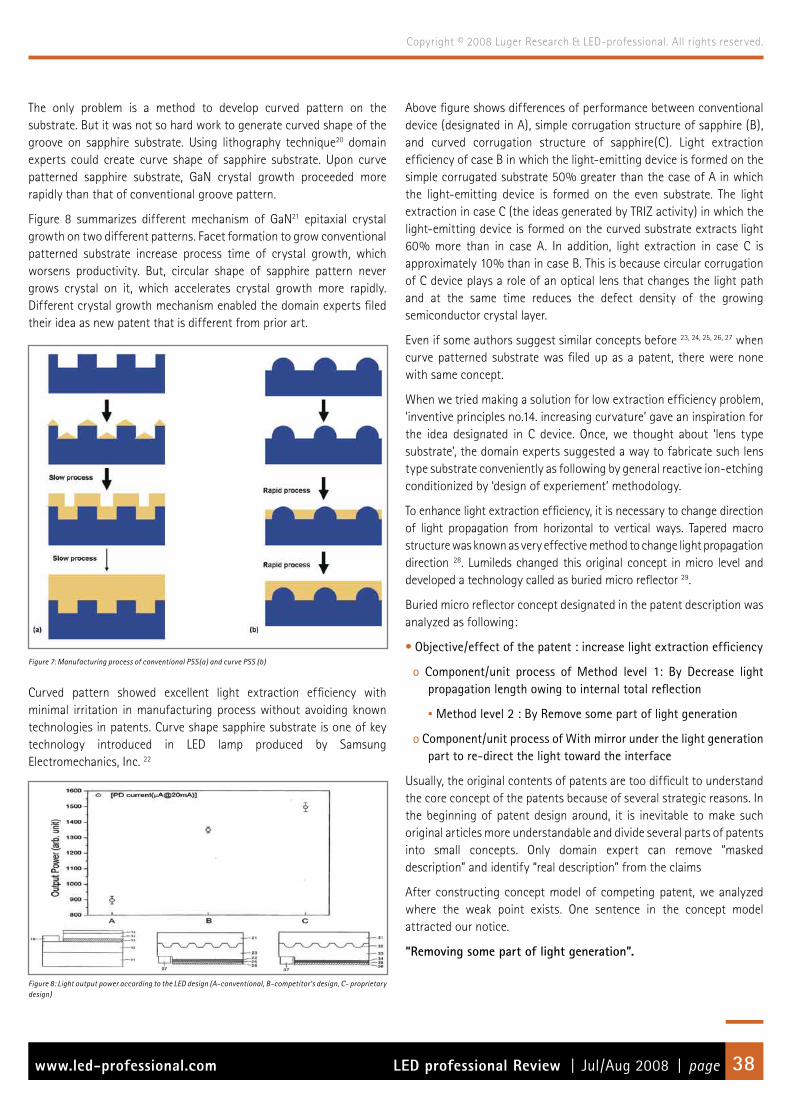
LED professional Review | Jul/Aug 2008 | pagewww.led-professional.com 38
Copyright © 2008 Luger Research & LED-professional. All rights reserved.
The only problem is a method to develop curved pattern on the substrate. But it was not so hard work to generate curved shape of the groove on sapphire substrate. Using lithography technique20 domain experts could create curve shape of sapphire substrate. Upon curve patterned sapphire substrate, GaN crystal growth proceeded more rapidly than that of conventional groove pattern.
Figure 8 summarizes different mechanism of GaN21 epitaxial crystal growth on two different patterns. Facet formation to grow conventional patterned substrate increase process time of crystal growth, which worsens productivity. But, circular shape of sapphire pattern never grows crystal on it, which accelerates crystal growth more rapidly. Different crystal growth mechanism enabled the domain experts filed their idea as new patent that is different from prior art.
Figure 7: Manufacturing process of conventional PSS(a) and curve PSS (b)
Curved pattern showed excellent light extraction efficiency with minimal irritation in manufacturing process without avoiding known technologies in patents. Curve shape sapphire substrate is one of key technology introduced in LED lamp produced by Samsung Electromechanics, Inc. 22
Figure 8: Light output power according to the LED design (A-conventional, B-competitor’s design, C- proprietary design)
Above figure shows differences of performance between conventional device (designated in A), simple corrugation structure of sapphire (B), and curved corrugation structure of sapphire(C). Light extraction efficiency of case B in which the light-emitting device is formed on the simple corrugated substrate 50% greater than the case of A in which the light-emitting device is formed on the even substrate. The light extraction in case C (the ideas generated by TRIZ activity) in which the light-emitting device is formed on the curved substrate extracts light 60% more than in case A. In addition, light extraction in case C is approximately 10% than in case B. This is because circular corrugation of C device plays a role of an optical lens that changes the light path and at the same time reduces the defect density of the growing semiconductor crystal layer.
Even if some authors suggest similar concepts before 23, 24, 25, 26, 27 when curve patterned substrate was filed up as a patent, there were none with same concept.
When we tried making a solution for low extraction efficiency problem, ‘inventive principles no.14. increasing curvature’ gave an inspiration for the idea designated in C device. Once, we thought about ‘lens type substrate’, the domain experts suggested a way to fabricate such lens type substrate conveniently as following by general reactive ion-etching conditionized by ‘design of experiement’ methodology.
To enhance light extraction efficiency, it is necessary to change direction of light propagation from horizontal to vertical ways. Tapered macro structure was known as very effective method to change light propagation direction 28. Lumileds changed this original concept in micro level and developed a technology called as buried micro reflector 29.
Buried micro reflector concept designated in the patent description was analyzed as following:
• Objective/effect of the patent : increase light extraction efficiency
o Component/unit process of Method level 1: By Decrease light propagation length owing to internal total reflection
▪ Method level 2 : By Remove some part of light generation
o Component/unit process of With mirror under the light generation part to re-direct the light toward the interface
Usually, the original contents of patents are too difficult to understand the core concept of the patents because of several strategic reasons. In the beginning of patent design around, it is inevitable to make such original articles more understandable and divide several parts of patents into small concepts. Only domain expert can remove “masked description” and identify “real description” from the claims
After constructing concept model of competing patent, we analyzed where the weak point exists. One sentence in the concept model attracted our notice.
“Removing some part of light generation”.
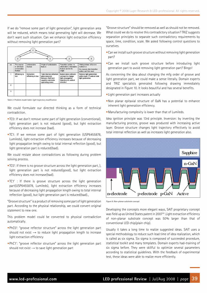
LED professional Review | Jul/Aug 2008 | pagewww.led-professional.com 39
Copyright © 2008 Luger Research & LED-professional. All rights reserved.
If we do “remove some part of light generation”, light generation area will be reduced, which means total generating light will decrease. We don’t want such situation. Can we enhance light extraction efficiency without removing light generation part?
Table 3: Problem model table: light trajectory modification
We could formulate our directed thinking as a form of technical contradiction.
• TC0: If we don’t remove some part of light generation (conventional), light generation part is not reduced (good), but light extraction efficiency does not increase (bad).
• TC1: If we remove some part of light generation (USP6455878, Lumileds), light extraction efficiency increases because of decreasing light propagation length owing to total internal reflection (good), but light generation part is reduced(bad).
We could restate above contradictions as following during problem solving process.
• TC0’: If there is no groove structure across the light generation part, ), light generation part is not reduced(good), but light extraction efficiency does not increase(bad).
• TC1’ : If there is groove structure across the light generation part(USP6455878, Lumileds), light extraction efficiency increases because of decreasing light propagation length owing to total internal reflection (good), but light generation part is reduced(bad).,
“Groove structure” is a product of removing some part of light generation part. According to the physical relationship, we could convert original statement to new one.
This problem model could be converted to physical contradiction automatically.
• PhC0’: “groove reflector structure” across the light generation part should not exist → to reduce light propagation length to increase light extraction efficiency
• PhC1’: “groove reflector structure” across the light generation part should not exist → to save light generation part
“Groove structure” should be removed as well as should not be removed. What could we do to resolve this contradictory situation? TRIZ suggests separation principles to separate such contradictory requirements by space, time, condition, scale. We asked following control questions to ourselves.
•Can we install such groove structure without removing light generation part?
• Can we install such groove structure before introducing light generation part to avoid removing light generation part? Bingo!
As concerning the idea about changing the mfg order of groove and light generation part, we could make a sense literally. Domain experts and TRIZ specialists generated following drawing immediately designated in Figure 10. It looks beautiful and has several benefits.
• Light generation part increases actually
• Non planar epitaxial structure of GaN has a potential to enhance inherent light generation efficiency.
• Manufacturing complexity is lower than that of Lumileds.
Idea ignition principle was 13rd principle. Inversion: by inverting the manufacturing process, groove was produced with increasing active layer. Groove structure changes light trajectory effectively to avoid total internal reflection as well as increases light generation also.
Figure 9: Non-planar substrate concept
Developing the concepts more elegant ways, SAIT proprietary concept was field up as United States patent in 200730 .Light extraction efficiency of non-planar substrate concept was 50% larger than that of conventional LED chip(plain chip).
Usually it takes a long time to realize suggested ideas. SAIT uses a special methodology to reduce such lead time of idea realization, which is called as six sigma. Six sigma is composed of succeeded procedure, statistical toolkit and many templates. Domain experts had-training of six sigma before. They were skillful to optimize several parameters according to statistical guidelines. With the feedback of experimental test, these ideas were able to realize more efficiently.
LED professional Review | Jul/Aug 2008 | pagewww.led-professional.com 40
Copyright © 2008 Luger Research & LED-professional. All rights reserved.
SummaryOne of critical problem in conventional GaN LED system was analyzed by TRIZ methodologies. After resource analysis, total internal reflection between GaN and sapphire substrate was recognized as most serious source of the low extraction efficiency problem. Known solutions, i.e. transition action for the total internal reflection were critically surveyed by problem formulating table. Contradictions caused by transition actions were formulated and resolved with guidance of inventive principles which suggest conceptual guideline for technical contradiction. More than 20 useful ideas were induced by referring to principles of TRIZ. Many ideas have shown excellent performance for light extraction up to 60% increase. 2 of them were filed up as US patent and applied as one of most important technology for real LED chip produced by SEMCO, Inc.
EpilogueThis project was executed in May to September in 2003. More than 25 technical ideas were suggested. 2 of them were filed up as international patent. Applying one concept created by this project was introduced in real LED system produced by Samsung Electromechanics, Inc. With TRIZ thinking process, the problem “light extraction efficiency of LED is low” could be understood more thoroughly, the solutions for the problem could be induced more easily than without TRIZ. LED division of SAMSUNG Electromechanics could release brighter LED based backlight unit for cell phone in 200631.
In the end of the TRIZ activity, TRIZ consultants forecasted the near future of LED system. According to the pattern of increasing segmentation level, light extraction structure will be smaller and smaller to nano-level. Current papers and patents are dealing with such nanostructure in many boundaries32. Rapid realization of the suggested ideas was conducted by statistical assistance of six sigma methodologies.
Acknowledgement:
Special thanks to Dr. Yoon, Suk Ho, Dr. Kim, Hyun Soo, Mr. Cho, Je Hee and Dr. Son, Chul Soo for their enthusiastic supports on the TRIZ activity, idea developing and realization. Special thanks to Mr. Cheong, Se Ho and all current and ex members of six sigma research group in SAIT.
References:
1 http://en.wikipedia.org/wiki/Light-emitting_diodes
2 Nakamura, S. et al, “Room-temperature continuous-wave operation of InGaN multi-quantum-well-structure laser diodes with a long lifetime”, Appl. Phys. Lett. Vol. 70, pp.868-870(1997).
3 Light Emitting Diodes (LEDs) for General Illumination, AN OIDA TECHNOLOGY ROADMAP UPDATE 2 0 0 2, http://lighting.sandia.gov/lightingdocs/JonesEDLEDRoadmap200103.pdf
4 Schubert EF, et al., “Solid-state lighting—a benevolent technology”, Rep Prog Phys. 69, pp3069-3099(2006).
5 Streubel K. et al., “ High brightness AlGaInP light-emitting diodes”, IEEE JOURNAL ON SELECTED TOPICS IN QUANTUM ELECTRONICS. 8(2) pp.321-332(2002).
6 Toshihiko Baba, et al., “Strong Enhancement of Light Extraction Efficiency in GaInAsP 2-D-Arranged Microcolumns”, JOURNAL OF LIGHTWAVE TECHNOLOGY, 17(11), pp.2113-2120, (1999).
7 Sven-Silvius Schad, “Extraction E±ciency of GaN-Based LEDs”, Optoelectronics Department, University of Ulm, Annual Report, pp.99-104 (2000).
8 YAMADA, M. et al., “InGaN-Based Near-Ultraviolet and Blue-Light-Emitting Diodes with high External Quantum Efficiency Using a Patterned Sapphire Substrate and a Mesh Electrode”, Jpn. J. Appl. Phys. Vol. 41 Part 2, No. 12B pp. L 1431–L 1433 (2002)
9 Innovation WorkBenchTM ver.2.8.0
10 Song, M.J. et al., “Step-by-step initial situation analysis logic.1. Formulating Technical Contradiction from Initial Situation, TRIZ-Journal, October 2004.
11 Kong, H. -S. et al, “Single step pendeo- and lateral epitaxial overgrowth of group III-nitride epitaxial layers with group III-nitride buffer layer and resulting structures”, United States Patent 6764932
12 Mukai, T. Et al. “Nitride light-emitting diodes”, J. Phys.: Condens. Matter, 13, pp.7089-7098(2001).
13 ROSKOWSKI, A. M. et al, “Maskless Pendeo-Epitaxial Growth of GaN Films”, Journal of Electronic Materials, 31(5), pp. 421 - 428 (2002).
14 JP 2002-280611
15 JP 2001-267242
16 Tadatomo, K. et al , “High output power InGaN ultravaiot light emitting diodes fabricated on patterned substrates using metalorganic vapor phase epitaxy”, Jpn J. Appl. Phys. Vol.40(Part, No 6B), pp.L583-L585, (2001).
17 Yamada, M. et al, “InGaN-based near-ultraviolet and blue-light-emitting diodes with high external quantum efficiency using a patterned sapphire substrate and a mesh electrode”, Jpn. J. Appl. Phys., vol. 41(no.12B), pp.L1431–L1433 (2002).
18 Song, M.J. et al., “Step-by-step initial situation analysis logic. I. Formulating Technical Contradiction from Initial Situation”, TRIZ-Journal, October 2004.
19 Mann, DL, “Matrix 2003, Updating the TRIZ Contradiction Matrix”, p.118, CREAX Press,, Belgium, 2003.
20 http://www.oichina.cn/product/oipt/News/lensetch.pdf
21 Light-emitting device and method of manufacturing the same, US Pub. No. 20050082546 (2005.04.21))
22 http://www.tech2.com/india/news/mobile-phones/Samsung%20Develops%20Brighter%20Phone%20Display/2516/0
23 Yamada, M., et al., “InGaN-based near-ultraviolet and blue-light-emitting diodes with high external quantum efficiency using a patterned sapphire substrate and a mesh electrode,” Jpn. J. Appl. Phys., vol. 41, pp. L1431–L1433, 2002.
24 Tadatomo, K., et al., “High output power near-ultraviolet and violet light-emitting diodes fabricated on patterned sapphire substrates using metalorganic vapor phase epitaxy,” Proc. SPIE, vol. 5187 pp. 243–249(2004).
25 Feng, Z. H., et al., “GaN-based blue light emitting diodes grown and fabricated on patterned sapphire substrates by metalorganic vapor-phase epitaxy,” J. Cryst. Growth, vol. 272, pp.327–332 (2004).
26 Lau, K.M. et al., “Enhanced Luminescence From GaN-Based Blue LEDs Grown on Grooved Sapphire Substrates”, IEEE PHOTONICS TECHNOLOGY LETTERS, VOL. 17 (9), pp.1812-1814(2005).
27 Chang, S. J. et al, “Patterned sapphire : MOCVD growth of InGaN/GaN blue light emitting diodes on patterned sapphire substrates”, Phys. Stat. Sol. (c) 0, No. 7, 2253–2256 (2003)
28 Schmid, W., et al., “Infrared Light-Emitting Diodes with Lateral Outcoupling Taper for High Extrac-tion E±ciency”, Light-Emitting Diodes: Research, Manufacturing, and Applications III, SPIE Proc., pp. 198-205, (1999)
29 Semiconductor LED flip-chip having low refractive index underfill, United States Patent 6455878
30 Light emitting diode and method of fabricating the same, USP publication no 20070012933
31 http://www.tech2.com/india/news/mobile-phones/Samsung%20Develops%20Brighter%20Phone%20Display/2516/0
32 Y. J. Lee, et al., “GaN-Based LEDs With Al-Deposited V-Shaped Sapphire Facet Mirror”, IEEE PHOTONICS TECHNOLOGY LETTERS, VOL.18 (5) pp.724-726 (2006)
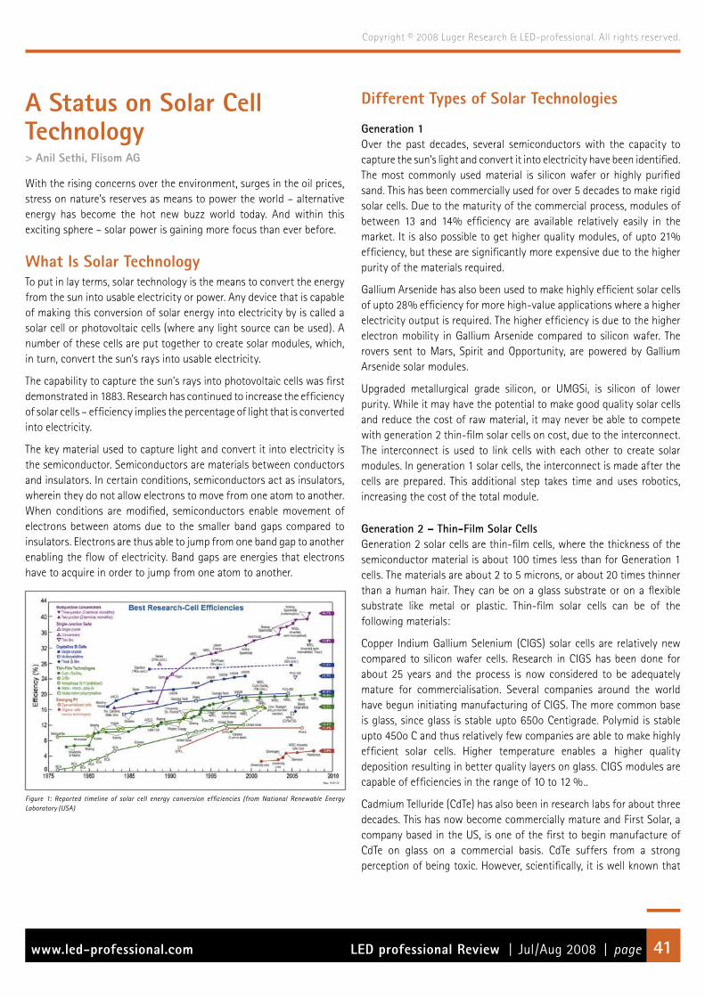
LED professional Review | Jul/Aug 2008 | pagewww.led-professional.com 41
Copyright © 2008 Luger Research & LED-professional. All rights reserved.
A Status on Solar Cell Technology> Anil Sethi, Flisom AG
With the rising concerns over the environment, surges in the oil prices, stress on nature’s reserves as means to power the world – alternative energy has become the hot new buzz world today. And within this exciting sphere – solar power is gaining more focus than ever before.
What Is Solar TechnologyTo put in lay terms, solar technology is the means to convert the energy from the sun into usable electricity or power. Any device that is capable of making this conversion of solar energy into electricity by is called a solar cell or photovoltaic cells (where any light source can be used). A number of these cells are put together to create solar modules, which, in turn, convert the sun’s rays into usable electricity.
The capability to capture the sun’s rays into photovoltaic cells was first demonstrated in 1883. Research has continued to increase the efficiency of solar cells – efficiency implies the percentage of light that is converted into electricity.
The key material used to capture light and convert it into electricity is the semiconductor. Semiconductors are materials between conductors and insulators. In certain conditions, semiconductors act as insulators, wherein they do not allow electrons to move from one atom to another. When conditions are modified, semiconductors enable movement of electrons between atoms due to the smaller band gaps compared to insulators. Electrons are thus able to jump from one band gap to another enabling the flow of electricity. Band gaps are energies that electrons have to acquire in order to jump from one atom to another.
Figure 1: Reported timeline of solar cell energy conversion efficiencies (from National Renewable Energy Laboratory (USA)
Different Types of Solar Technologies
Generation 1Over the past decades, several semiconductors with the capacity to capture the sun’s light and convert it into electricity have been identified. The most commonly used material is silicon wafer or highly purified sand. This has been commercially used for over 5 decades to make rigid solar cells. Due to the maturity of the commercial process, modules of between 13 and 14% efficiency are available relatively easily in the market. It is also possible to get higher quality modules, of upto 21% efficiency, but these are significantly more expensive due to the higher purity of the materials required.
Gallium Arsenide has also been used to make highly efficient solar cells of upto 28% efficiency for more high-value applications where a higher electricity output is required. The higher efficiency is due to the higher electron mobility in Gallium Arsenide compared to silicon wafer. The rovers sent to Mars, Spirit and Opportunity, are powered by Gallium Arsenide solar modules.
Upgraded metallurgical grade silicon, or UMGSi, is silicon of lower purity. While it may have the potential to make good quality solar cells and reduce the cost of raw material, it may never be able to compete with generation 2 thin-film solar cells on cost, due to the interconnect. The interconnect is used to link cells with each other to create solar modules. In generation 1 solar cells, the interconnect is made after the cells are prepared. This additional step takes time and uses robotics, increasing the cost of the total module.
Generation 2 – Thin-Film Solar CellsGeneration 2 solar cells are thin-film cells, where the thickness of the semiconductor material is about 100 times less than for Generation 1 cells. The materials are about 2 to 5 microns, or about 20 times thinner than a human hair. They can be on a glass substrate or on a flexible substrate like metal or plastic. Thin-film solar cells can be of the following materials:
Copper Indium Gallium Selenium (CIGS) solar cells are relatively new compared to silicon wafer cells. Research in CIGS has been done for about 25 years and the process is now considered to be adequately mature for commercialisation. Several companies around the world have begun initiating manufacturing of CIGS. The more common base is glass, since glass is stable upto 650o Centigrade. Polymid is stable upto 450o C and thus relatively few companies are able to make highly efficient solar cells. Higher temperature enables a higher quality deposition resulting in better quality layers on glass. CIGS modules are capable of efficiencies in the range of 10 to 12 %..
Cadmium Telluride (CdTe) has also been in research labs for about three decades. This has now become commercially mature and First Solar, a company based in the US, is one of the first to begin manufacture of CdTe on glass on a commercial basis. CdTe suffers from a strong perception of being toxic. However, scientifically, it is well known that
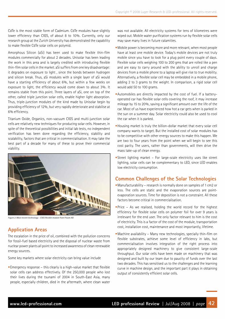
LED professional Review | Jul/Aug 2008 | pagewww.led-professional.com 42
Copyright © 2008 Luger Research & LED-professional. All rights reserved.
CdTe is the most stable form of Cadmium. CdTe modules have slightly lower efficiency than CIGS, of about 8 to 10%. Currently, only our research group at the Zurich University has demonstrated the capability to make flexible CdTe solar cells on polymid.
Amorphous Silicon (aSi) has been used to make flexible thin-film modules commercially for about 2 decades. Unisolar has been leading the work in this area and is largely credited with introducing flexible thin-film solar cells in the market. aSi suffers from one key disadvantage: it degrades on exposure to light , since the bonds between hydrogen and silicon break. Thus, aSi modules with a single layer of aSi would have a starting efficiency of about 6%, but within a few weeks on exposure to light, the efficiency would come down to about 3%. It remains stable from this point. Three layers of aSi, one on top of the other, called triple junction solar cells, enable higher light absorption. Thus, triple-junction modules of the kind made by Unisolar begin by providing efficiency of 12%, but very rapidly deteriorate and stabilise at 6% efficiency.
Titanium Oxide, Organics, non-vacuum CIGS and multi-junction solar cells are relatively new techniques for producing solar cells. However, in spite of the theoretical possibilities and initial lab tests, no independent verification has been done regarding the efficiency, stability and scalability, factors that are critical in commercialisation. It may take the best part of a decade for many of these to prove their commercial viability.
Figure 2: Most recent technology - CIGS flexible module from Flisom AG
Application Areas The escalation in the price of oil, combined with the pollution concerns for fossil-fuel based electricity and the disposal of nuclear waste from nuclear power plants all point to increased awareness of clean renewable energy sources.
Some key markets where solar electricity can bring value include
• Emergency response – this clearly is a high-value market that flexible solar cells can address effectively. Of the 250,000 people who lost their lives during the tsunami of 2004 in South-East Asia, many people, especially children, died in the aftermath, where clean water
was not available. All electricity systems for tens of kilometres were wiped out. Mobile water purification systems run by flexible solar cells may save many lives in future calamities.
• Mobile power is becoming more and more relevant, when most people have at least one mobile device. Today’s mobile devices are not truly mobile since you have to look for a plug point every couple of days. Flexible solar cells weighing 100 to 200 gms that are rolled like a pen and are easy to carry around with the ability to unroll and charge devices from a mobile phone to a laptop will give rise to true mobility. Alternatively, a flexible solar cell may be embedded in a mobile phone, adding 2 to 3 grams to the weight. In comparison, a rigid solar cell would add 50 to 100 grams.
•Automobiles are directly impacted by the cost of fuel. If a battery-operated car has flexible solar cells covering the roof, it may increase mileage by 15 to 20%, saving a significant amount over the life of the car. Most of us have experienced how hot a car gets when is parked in the sun on a summer day. Solar electricity could also be used to cool the car when it is parked.
•Housing market is truly the billion-dollar market that every solar cell company wants to target. But the installed cost of solar modules has to be competitive with other energy sources to make this happen. We are two to four years from the point when we will begin to see this cost parity. The users, rather than governments, will then drive the mass take-up of clean energy.
• Street lighting market – For large-scale electricity uses like street lighting, solar cells can be complementary to LED, since LED enables low electricity consumption.
Common Challenges of the Solar Technologies•Manufacturability – research is normally done on samples of 1 cm2 or
less. The cells are static and the evaporation sources are point-evaporation sources. Time for deposition is not a constraint. All these factors become critical in commercialisation.
•Price – As we realised, holding the world record for the highest efficiency for flexible solar cells on polymer foil for over 9 years is irrelevant for the end user. The only factor relevant to him is the cost of electricity. This is a factor of the cost of the module, transportation cost, installation cost, maintenance and most importantly, lifetime.
• Machine availability – Many new technologies, specially thin-film on flexible substrates, achieve some level of efficiency in labs, but commercialisation involves integration of the right process into appropriately designed machinery to give consistent large-scale throughput. Our solar cells have been made on machinery that was designed and built by our team due to paucity of funds over the last two decades. This has sensitised us to the challenges and the learning curve in machine design, and the important part it plays in obtaining output of consistently efficient solar cells.
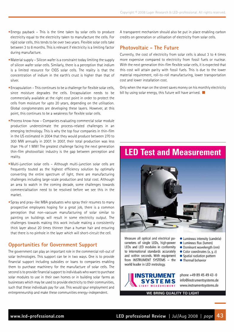
LED professional Review | Jul/Aug 2008 | pagewww.led-professional.com 43
Copyright © 2008 Luger Research & LED-professional. All rights reserved.
• Energy payback – This is the time taken by solar cells to produce electricity equal to the electricity taken to manufacture the cells. For rigid solar cells, this tends to be over two years. Flexible solar cells take between 3 to 8 months. This is relevant if electricity is a limiting factor during manufacture.
• Material supply – Silicon wafer is a constraint today limiting the supply of silicon wafer solar cells. Similarly, there is a perception that indium is a limited resource for CIGS solar cells. The reality is that the concentration of indium in the earth’s crust is higher than that of silver.
• Encapsulation – This continues to be a challenge for flexible solar cells, since moisture degrades the cells. Encapsulation needs to be commercially available at the right cost point in order to protect the cells from moisture for upto 20 years, depending on the utilisation. Global conglomerates are developing these layers. However, at this point, this continues to be a weakness for flexible solar cells.
• Process know-how – Companies evaluating commercial solar module production underestimate the process-related challenges in an emerging technology. This is why the top four companies in thin-film in the US estimated in 2004 that they would produce between 270 to 300 MW annually in 2007. In 2007, their total production was less than 1% of 1 MW! The greatest challenge facing the next generation thin-film photovoltaic industry is the gap between perception and reality.
• Multi-junction solar cells – Although multi-junction solar cells are frequently touted as the highest efficiency solution by optimally converting the entire spectrum of light, there are manufacturing challenges including large-scale production and total cost. Although an area to watch in the coming decade, some challenges towards commercialisation need to be resolved before we see this in the market.
•Spray and pray–like MBA graduates who spray their resumes to many prospective employees hoping for a great job, there is a common perception that non–vacuum manufacturing of solar similar to painting on buildings will result in some electricity output. The challenges towards making this work include making a consistently thick layer about 20 times thinner than a human hair and ensuring that there is no pinhole in the layer which will short-circuit the cell.
Opportunities for Government SupportThe government can play an important role in the commercial roll-out of solar technologies. This support can be in two ways. One is to provide financial support including subsidies or loans to companies enabling them to purchase machinery for the manufacture of solar cells. The second is to provide financial support to individuals who want to purchase solar modules to use in their own homes or in building solar farms as businesses which may be used to provide electricity to their communities, such that these individuals pay for use. This would spur employment and entrepreneurship and make these communities energy-independent.
A transparent mechanism should also be put in place enabling carbon credits on generation or utilisation of electricity from solar cells.
Photovoltaic - The FutureCurrently, the cost of electricity from solar cells is about 3 to 4 times more expensive compared to electricity from fossil fuels or nuclear. With the next generation thin-film flexible solar cells, it is expected that this cost will attain parity with fossil fuels. This is due to the lower material requirement, roll-to-roll manufacturing, lower transportation cost and lower installation cost.
Only when the man on the street saves money on his monthly electricity bill by using solar energy, this future will have arrived.
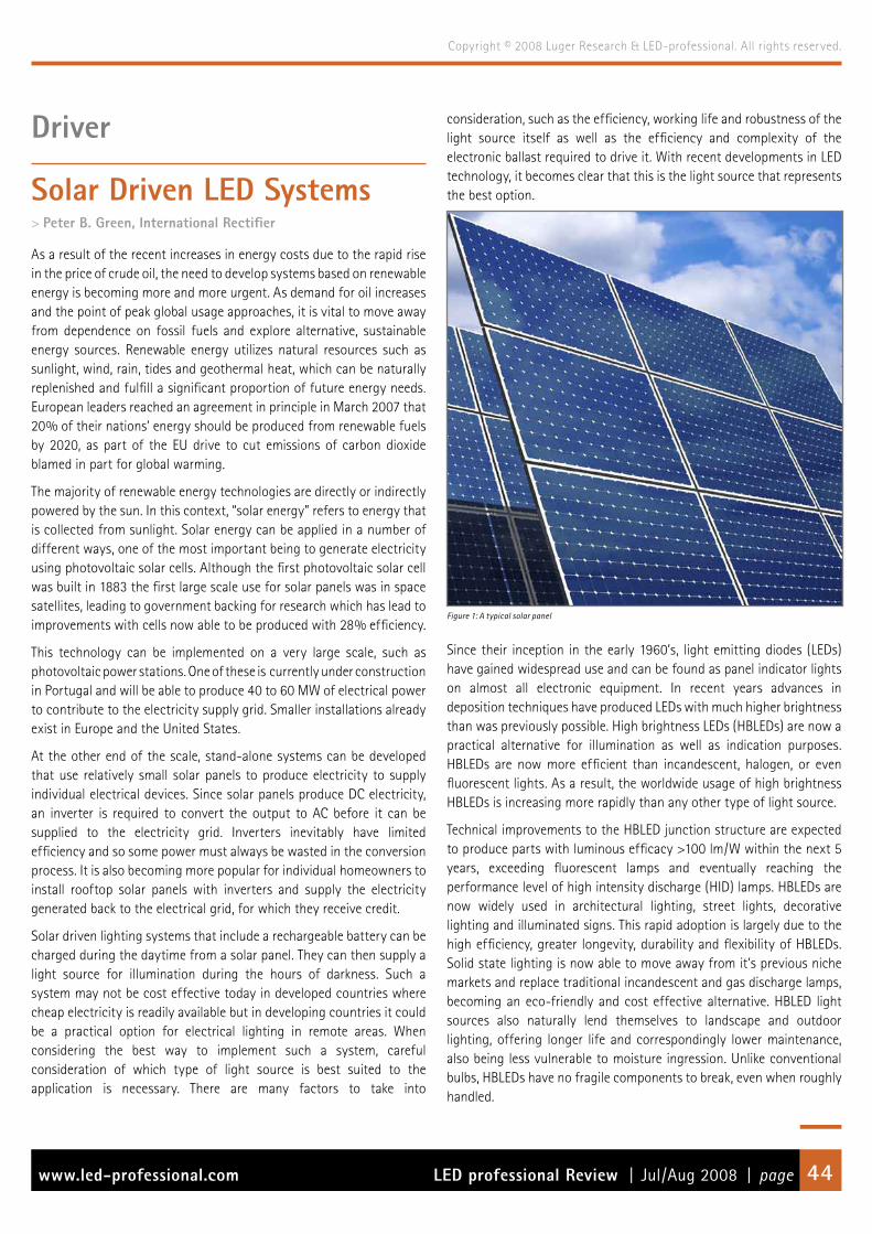
LED professional Review | Jul/Aug 2008 | pagewww.led-professional.com 44
Copyright © 2008 Luger Research & LED-professional. All rights reserved.
Driver
Solar Driven LED Systems> Peter B. Green, International Rectifier
As a result of the recent increases in energy costs due to the rapid rise in the price of crude oil, the need to develop systems based on renewable energy is becoming more and more urgent. As demand for oil increases and the point of peak global usage approaches, it is vital to move away from dependence on fossil fuels and explore alternative, sustainable energy sources. Renewable energy utilizes natural resources such as sunlight, wind, rain, tides and geothermal heat, which can be naturally replenished and fulfill a significant proportion of future energy needs. European leaders reached an agreement in principle in March 2007 that 20% of their nations’ energy should be produced from renewable fuels by 2020, as part of the EU drive to cut emissions of carbon dioxide blamed in part for global warming.
The majority of renewable energy technologies are directly or indirectly powered by the sun. In this context, “solar energy” refers to energy that is collected from sunlight. Solar energy can be applied in a number of different ways, one of the most important being to generate electricity using photovoltaic solar cells. Although the first photovoltaic solar cell was built in 1883 the first large scale use for solar panels was in space satellites, leading to government backing for research which has lead to improvements with cells now able to be produced with 28% efficiency.
This technology can be implemented on a very large scale, such as photovoltaic power stations. One of these is currently under construction in Portugal and will be able to produce 40 to 60 MW of electrical power to contribute to the electricity supply grid. Smaller installations already exist in Europe and the United States.
At the other end of the scale, stand-alone systems can be developed that use relatively small solar panels to produce electricity to supply individual electrical devices. Since solar panels produce DC electricity, an inverter is required to convert the output to AC before it can be supplied to the electricity grid. Inverters inevitably have limited efficiency and so some power must always be wasted in the conversion process. It is also becoming more popular for individual homeowners to install rooftop solar panels with inverters and supply the electricity generated back to the electrical grid, for which they receive credit.
Solar driven lighting systems that include a rechargeable battery can be charged during the daytime from a solar panel. They can then supply a light source for illumination during the hours of darkness. Such a system may not be cost effective today in developed countries where cheap electricity is readily available but in developing countries it could be a practical option for electrical lighting in remote areas. When considering the best way to implement such a system, careful consideration of which type of light source is best suited to the application is necessary. There are many factors to take into
consideration, such as the efficiency, working life and robustness of the light source itself as well as the efficiency and complexity of the electronic ballast required to drive it. With recent developments in LED technology, it becomes clear that this is the light source that represents the best option.
Figure 1: A typical solar panel
Since their inception in the early 1960’s, light emitting diodes (LEDs) have gained widespread use and can be found as panel indicator lights on almost all electronic equipment. In recent years advances in deposition techniques have produced LEDs with much higher brightness than was previously possible. High brightness LEDs (HBLEDs) are now a practical alternative for illumination as well as indication purposes. HBLEDs are now more efficient than incandescent, halogen, or even fluorescent lights. As a result, the worldwide usage of high brightness HBLEDs is increasing more rapidly than any other type of light source.
Technical improvements to the HBLED junction structure are expected to produce parts with luminous efficacy >100 lm/W within the next 5 years, exceeding fluorescent lamps and eventually reaching the performance level of high intensity discharge (HID) lamps. HBLEDs are now widely used in architectural lighting, street lights, decorative lighting and illuminated signs. This rapid adoption is largely due to the high efficiency, greater longevity, durability and flexibility of HBLEDs. Solid state lighting is now able to move away from it’s previous niche markets and replace traditional incandescent and gas discharge lamps, becoming an eco-friendly and cost effective alternative. HBLED light sources also naturally lend themselves to landscape and outdoor lighting, offering longer life and correspondingly lower maintenance, also being less vulnerable to moisture ingression. Unlike conventional bulbs, HBLEDs have no fragile components to break, even when roughly handled.
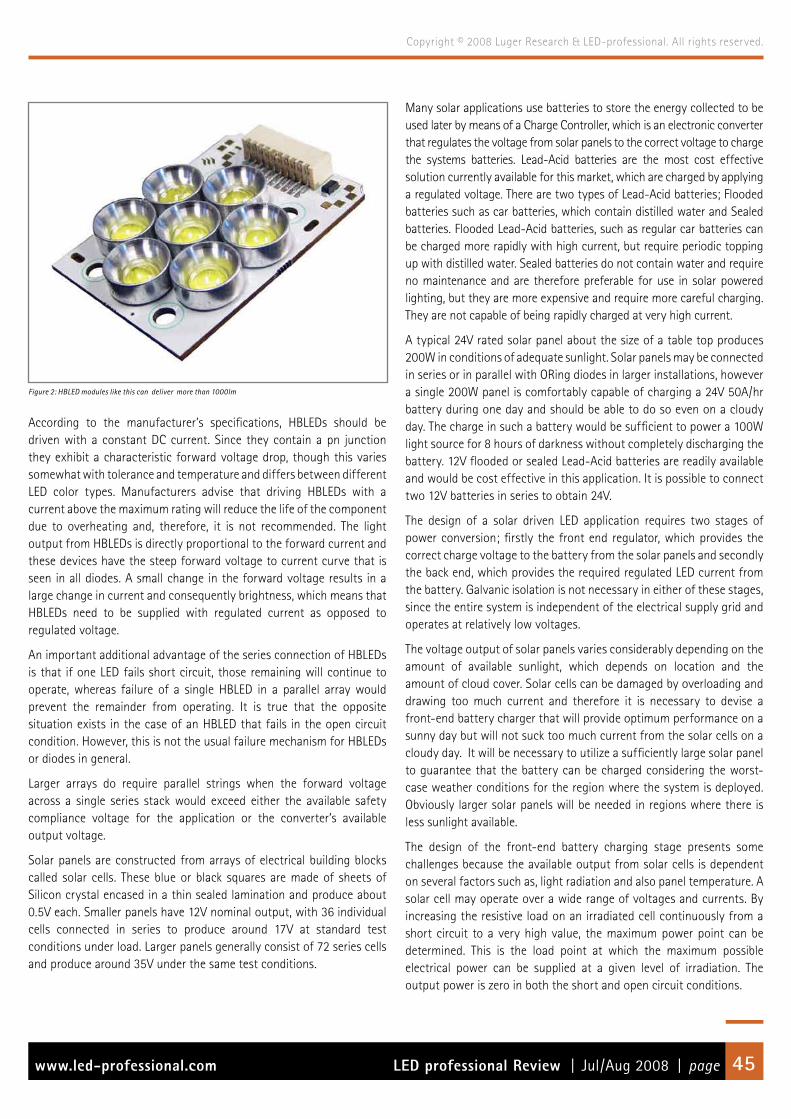
LED professional Review | Jul/Aug 2008 | pagewww.led-professional.com 45
Copyright © 2008 Luger Research & LED-professional. All rights reserved.
Figure 2: HBLED modules like this can deliver more than 1000lm
According to the manufacturer’s specifications, HBLEDs should be driven with a constant DC current. Since they contain a pn junction they exhibit a characteristic forward voltage drop, though this varies somewhat with tolerance and temperature and differs between different LED color types. Manufacturers advise that driving HBLEDs with a current above the maximum rating will reduce the life of the component due to overheating and, therefore, it is not recommended. The light output from HBLEDs is directly proportional to the forward current and these devices have the steep forward voltage to current curve that is seen in all diodes. A small change in the forward voltage results in a large change in current and consequently brightness, which means that HBLEDs need to be supplied with regulated current as opposed to regulated voltage.
An important additional advantage of the series connection of HBLEDs is that if one LED fails short circuit, those remaining will continue to operate, whereas failure of a single HBLED in a parallel array would prevent the remainder from operating. It is true that the opposite situation exists in the case of an HBLED that fails in the open circuit condition. However, this is not the usual failure mechanism for HBLEDs or diodes in general.
Larger arrays do require parallel strings when the forward voltage across a single series stack would exceed either the available safety compliance voltage for the application or the converter’s available output voltage.
Solar panels are constructed from arrays of electrical building blocks called solar cells. These blue or black squares are made of sheets of Silicon crystal encased in a thin sealed lamination and produce about 0.5V each. Smaller panels have 12V nominal output, with 36 individual cells connected in series to produce around 17V at standard test conditions under load. Larger panels generally consist of 72 series cells and produce around 35V under the same test conditions.
Many solar applications use batteries to store the energy collected to be used later by means of a Charge Controller, which is an electronic converter that regulates the voltage from solar panels to the correct voltage to charge the systems batteries. Lead-Acid batteries are the most cost effective solution currently available for this market, which are charged by applying a regulated voltage. There are two types of Lead-Acid batteries; Flooded batteries such as car batteries, which contain distilled water and Sealed batteries. Flooded Lead-Acid batteries, such as regular car batteries can be charged more rapidly with high current, but require periodic topping up with distilled water. Sealed batteries do not contain water and require no maintenance and are therefore preferable for use in solar powered lighting, but they are more expensive and require more careful charging. They are not capable of being rapidly charged at very high current.
A typical 24V rated solar panel about the size of a table top produces 200W in conditions of adequate sunlight. Solar panels may be connected in series or in parallel with ORing diodes in larger installations, however a single 200W panel is comfortably capable of charging a 24V 50A/hr battery during one day and should be able to do so even on a cloudy day. The charge in such a battery would be sufficient to power a 100W light source for 8 hours of darkness without completely discharging the battery. 12V flooded or sealed Lead-Acid batteries are readily available and would be cost effective in this application. It is possible to connect two 12V batteries in series to obtain 24V.
The design of a solar driven LED application requires two stages of power conversion; firstly the front end regulator, which provides the correct charge voltage to the battery from the solar panels and secondly the back end, which provides the required regulated LED current from the battery. Galvanic isolation is not necessary in either of these stages, since the entire system is independent of the electrical supply grid and operates at relatively low voltages.
The voltage output of solar panels varies considerably depending on the amount of available sunlight, which depends on location and the amount of cloud cover. Solar cells can be damaged by overloading and drawing too much current and therefore it is necessary to devise a front-end battery charger that will provide optimum performance on a sunny day but will not suck too much current from the solar cells on a cloudy day. It will be necessary to utilize a sufficiently large solar panel to guarantee that the battery can be charged considering the worst-case weather conditions for the region where the system is deployed. Obviously larger solar panels will be needed in regions where there is less sunlight available.
The design of the front-end battery charging stage presents some challenges because the available output from solar cells is dependent on several factors such as, light radiation and also panel temperature. A solar cell may operate over a wide range of voltages and currents. By increasing the resistive load on an irradiated cell continuously from a short circuit to a very high value, the maximum power point can be determined. This is the load point at which the maximum possible electrical power can be supplied at a given level of irradiation. The output power is zero in both the short and open circuit conditions.

LED professional Review | Jul/Aug 2008 | pagewww.led-professional.com 46
Copyright © 2008 Luger Research & LED-professional. All rights reserved.
Figure 3: Current-voltage characteristic of a Silicon solar cell from www.solarserver.de
If a 24V rated solar panel is used for this application, the actual voltage that it produces is around 35V. If rated at 200W such a panel would normally be able to produce a current of about 5A.
If the system uses a 24V rated lead-acid battery or combination of batteries, the charge voltage required is nominally 28.8V, therefore the front-end regulator will need to provide lower output voltage than input voltage, which will determine the choice of topology used. A 50A/hr sealed lead-acid battery could be safely charged with 5A current, which would take 10 hours to charge to full capacity.
Considering these factors and that isolation is not necessary it appears that a Buck topology is ideally suited for the front end regulator. This regulator should include circuitry to provide a constant output voltage and limit the charge current, at the same time limiting the current drawn from the solar panel.
The Buck regulator offers the advantage of simplicity, as it is able to provide current limiting and output voltage regulation with a single PWM switching device, while possessing inherent short circuit protection.
Figure 4: Schematic of Buck regulator battery charger (original)
It can be safely assumed for this application that the LEDs will never need to be lit while the battery is being charged, which means that the front-end can be designed as a battery charger only without needing to be capable of driving the output load at the same time . This allows the dimensioning of the power semiconductors and inductors (as well as the solar panel) to remain relatively small, saving on cost and maintaining reduced size.
The LEDs will be illuminated during the hours of darkness when the battery is not being charged. Control can be accomplished by sensing the ambient light level with a photo sensor and shutting off the battery charger when this drops below a certain level, perhaps combining this with an electronic timer. At switchover the back end converter can be activated to provide a constant current drive to the LEDs from the battery.
The design of the back end LED drive stage requires a different set of considerations to be taken into account and is perhaps less straightforward to design than the front-end, since there are a number of configuration options available from which to create a panel of LEDs to provide a combined electrical load of 100W. HBLED arrays usually consist of several strings of series LEDs connected in parallel to create an array.
Figure 5: Schematic of HBLED panel – www.luxeon.com
Such an array of LEDs can be organized to have a voltage lower or higher than the battery voltage, in which case a Buck-Boost or Flyback topology would be required. If however the LED array were to be configured deliberately in such a way that the required voltage to supply it is always guaranteed to be higher than the battery voltage, then a Boost topology could also be used to supply the LEDs. In this case the design could be greatly simplified to provide a constant output current at higher output voltage than input voltage. Though short circuit protection is not possible with a Boost converter, the addition of a circuit breaker would provide this if needed.
Based on this approach, a good compromise for the LED array voltage in this example would be 48V, which is within safety low voltage limits and possesses no risk of electric shock to the user. This is also substantially above the 12V or 24V battery voltage making it suitable to use with a Boost regulator. The forward voltage drop of a single HBLED is approximately 4V and therefore 12 series LEDs would provide a combined forward voltage of 48V. If each of these LEDs were rated at 3W (a standard HBLED size) then the string would produce 36W of output at 700mA and three parallel strings would be required to obtain a total power of approximately 100W. It should be noted that since the
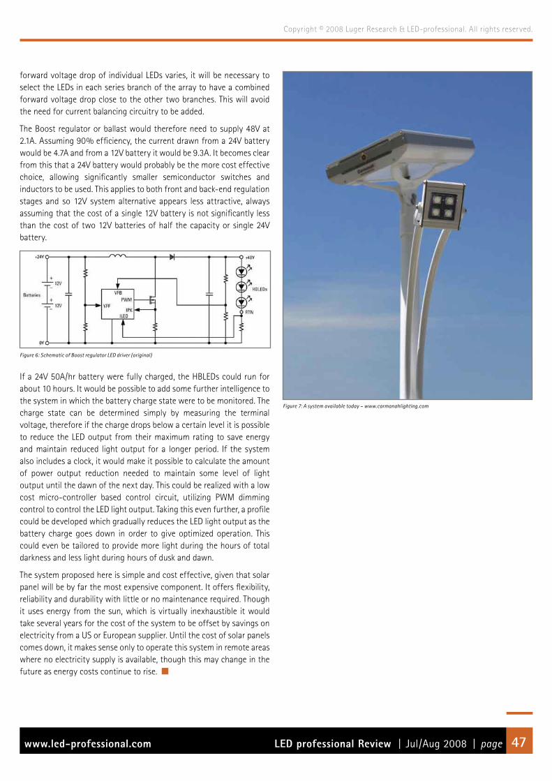
LED professional Review | Jul/Aug 2008 | pagewww.led-professional.com 47
Copyright © 2008 Luger Research & LED-professional. All rights reserved.
forward voltage drop of individual LEDs varies, it will be necessary to select the LEDs in each series branch of the array to have a combined forward voltage drop close to the other two branches. This will avoid the need for current balancing circuitry to be added.
The Boost regulator or ballast would therefore need to supply 48V at 2.1A. Assuming 90% efficiency, the current drawn from a 24V battery would be 4.7A and from a 12V battery it would be 9.3A. It becomes clear from this that a 24V battery would probably be the more cost effective choice, allowing significantly smaller semiconductor switches and inductors to be used. This applies to both front and back-end regulation stages and so 12V system alternative appears less attractive, always assuming that the cost of a single 12V battery is not significantly less than the cost of two 12V batteries of half the capacity or single 24V battery.
Figure 6: Schematic of Boost regulator LED driver (original)
If a 24V 50A/hr battery were fully charged, the HBLEDs could run for about 10 hours. It would be possible to add some further intelligence to the system in which the battery charge state were to be monitored. The charge state can be determined simply by measuring the terminal voltage, therefore if the charge drops below a certain level it is possible to reduce the LED output from their maximum rating to save energy and maintain reduced light output for a longer period. If the system also includes a clock, it would make it possible to calculate the amount of power output reduction needed to maintain some level of light output until the dawn of the next day. This could be realized with a low cost micro-controller based control circuit, utilizing PWM dimming control to control the LED light output. Taking this even further, a profile could be developed which gradually reduces the LED light output as the battery charge goes down in order to give optimized operation. This could even be tailored to provide more light during the hours of total darkness and less light during hours of dusk and dawn.
The system proposed here is simple and cost effective, given that solar panel will be by far the most expensive component. It offers flexibility, reliability and durability with little or no maintenance required. Though it uses energy from the sun, which is virtually inexhaustible it would take several years for the cost of the system to be offset by savings on electricity from a US or European supplier. Until the cost of solar panels comes down, it makes sense only to operate this system in remote areas where no electricity supply is available, though this may change in the future as energy costs continue to rise.
Figure 7: A system available today – www.carmanahlighting.com
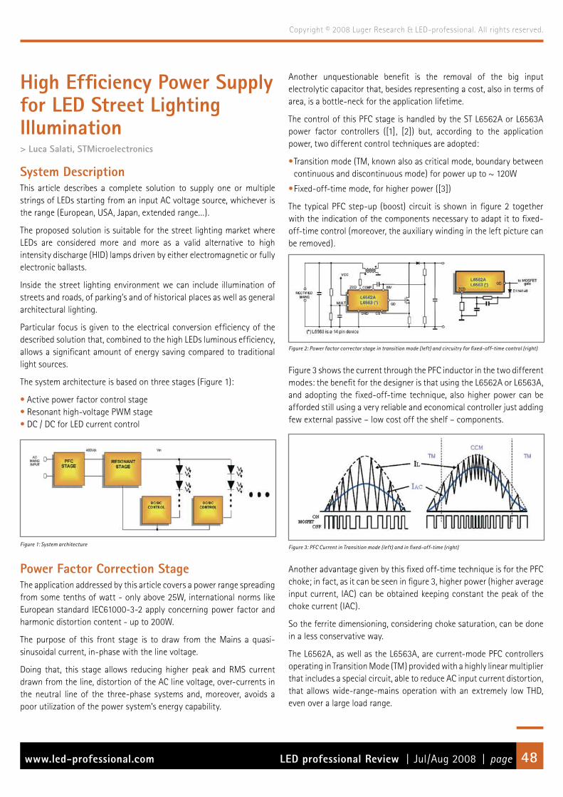
LED professional Review | Jul/Aug 2008 | pagewww.led-professional.com 48
Copyright © 2008 Luger Research & LED-professional. All rights reserved.
High Efficiency Power Supply for LED Street Lighting Illumination> Luca Salati, STMicroelectronics
System DescriptionThis article describes a complete solution to supply one or multiple strings of LEDs starting from an input AC voltage source, whichever is the range (European, USA, Japan, extended range…).
The proposed solution is suitable for the street lighting market where LEDs are considered more and more as a valid alternative to high intensity discharge (HID) lamps driven by either electromagnetic or fully electronic ballasts.
Inside the street lighting environment we can include illumination of streets and roads, of parking’s and of historical places as well as general architectural lighting.
Particular focus is given to the electrical conversion efficiency of the described solution that, combined to the high LEDs luminous efficiency, allows a significant amount of energy saving compared to traditional light sources.
The system architecture is based on three stages (Figure 1):
• Active power factor control stage• Resonant high-voltage PWM stage• DC / DC for LED current control
Figure 1: System architecture
Power Factor Correction StageThe application addressed by this article covers a power range spreading from some tenths of watt - only above 25W, international norms like European standard IEC61000-3-2 apply concerning power factor and harmonic distortion content - up to 200W.
The purpose of this front stage is to draw from the Mains a quasi-sinusoidal current, in-phase with the line voltage.
Doing that, this stage allows reducing higher peak and RMS current drawn from the line, distortion of the AC line voltage, over-currents in the neutral line of the three-phase systems and, moreover, avoids a poor utilization of the power system’s energy capability.
Another unquestionable benefit is the removal of the big input electrolytic capacitor that, besides representing a cost, also in terms of area, is a bottle-neck for the application lifetime.
The control of this PFC stage is handled by the ST L6562A or L6563A power factor controllers ([1], [2]) but, according to the application power, two different control techniques are adopted:
• Transition mode (TM, known also as critical mode, boundary between continuous and discontinuous mode) for power up to ~ 120W
• Fixed-off-time mode, for higher power ([3])
The typical PFC step-up (boost) circuit is shown in figure 2 together with the indication of the components necessary to adapt it to fixed-off-time control (moreover, the auxiliary winding in the left picture can be removed).
Figure 2: Power factor corrector stage in transition mode (left) and circuitry for fixed-off-time control (right)
Figure 3 shows the current through the PFC inductor in the two different modes: the benefit for the designer is that using the L6562A or L6563A, and adopting the fixed-off-time technique, also higher power can be afforded still using a very reliable and economical controller just adding few external passive – low cost off the shelf – components.
Figure 3: PFC Current in Transition mode (left) and in fixed-off-time (right)
Another advantage given by this fixed off-time technique is for the PFC choke; in fact, as it can be seen in figure 3, higher power (higher average input current, IAC) can be obtained keeping constant the peak of the choke current (IAC).
So the ferrite dimensioning, considering choke saturation, can be done in a less conservative way.
The L6562A, as well as the L6563A, are current-mode PFC controllers operating in Transition Mode (TM) provided with a highly linear multiplier that includes a special circuit, able to reduce AC input current distortion, that allows wide-range-mains operation with an extremely low THD, even over a large load range.

LED professional Review | Jul/Aug 2008 | pagewww.led-professional.com 49
Copyright © 2008 Luger Research & LED-professional. All rights reserved.
The output voltage is controlled by means of a voltage-mode error amplifier and an accurate internal voltage reference.
The devices feature extremely low consumption and include a disable function suitable for IC remote ON/OFF, which makes it easier to comply with energy saving requirements (Blue Angel, EnergyStar, ...).
While the L6562A is housed in 8 pin package (either DIP or SMD) offering basic functions, the L6563 is into 14 pins packages: besides the same L6562A core, it provides auxiliary functions such as input under-voltage detection, voltage feed-forward and, very important from to improve the solution effectiveness, the interfaces with the downstream controllers to manage in safe way critical phases like start-up, shut-down and failures.
Table 1, as an example, shows the performances in terms of power factor and total harmonic distortion for 80W application at full load.
Vin Efficiency PF THD90 93.4 0.999 3.7
115 95.2 0.998 4.3
135 95.8 0.997 4.8
180 96.1 0.993 6.0
230 95.5 0.984 7.7
265 95.1 0.974 9.5Table 1: Performances in terms of power factor and total harmonic distortion for 80W
According to the application power, operating temperature and used technique (transition mode or fixed-off-time), a suitable 500V or 600V breakdown MOSFET has to be chosen in order to optimize the efficiency of the solution.
Transition mode is working in zero-voltage switching so the conduction losses contribution is the most critical aspect at full load, while switching losses can be almost neglected. In fixed-off-time, instead, besides conduction losses, we have to consider switching losses as well the losses related to the recovery of the boost diode.
Examples of suitable part numbers for this application are STP12NM50/60 which provides very low Rds(on) combined with good dynamic behavior.
Resonant StageBecause of the much high efficiency that can be achieved (higher than the traditional PWM) and the reduction of the high frequency electromagnetic interference (thanks to the utilization of parasitic parameters of the circuit), the interest for resonant topologies is recently growing in power conversion market where requirements - both voluntary and mandatory – on efficiency and power density of their SMPS are getting tougher and tougher.
In fact this topology allows high power/weight ratio and low power dissipation of the power parts.
The device suitable for this conversion is the ST L6599 [4] [5], a high-voltage half-bridge resonant controller (Figure 4): rich in functions and robust in design, the device operates at 50% complementary duty-cycle with a fixed dead-time inserted to ensure soft-switching. The purpose of this intermediate stage is to convert the PFC output voltage into a lower level regulated voltage, which value depends on the:
• regulations for safety (SELV, isolation class)
•maximum number of LEDs to be placed in series
Figure 4: Resonant stage architecture
The energy throughput is controlled by varying the switching frequency that can be as high as 500kHz; isolation is provided on both the direct path (via a transformer) and the feedback path (via an opto-coupler)
The L6599 controls a MOSFETs half bridge: to drive the high-side switch with the bootstrap approach, the new device combines a high-voltage floating structure, able to withstand more than 600V, with an integrated bootstrap diode.
A non linear soft-start prevents inrush current and minimizes output-voltage overshoot. The device also features a controlled burst-mode operation, thus considerably reducing the average switching frequency and the associated losses under lightly loaded or unloaded conditions.
Particularly suitable when operating with an upstream PFC controller as a dedicated output enables the IC to switch off the Power Factor Corrector (PFC) pre-regulator during burst-mode operation – and also in case of faults – hence eliminating the no-load consumption of this stage.
Other key features of the L6599 are low power consumption (< 30mW), guaranteed latch-up free operation with slew rates up to 50V/ns, a not-latched disable input, and a high-performance Over-Current Protection (OCP) providing complete protection against both overload and short circuits. An additional latched disable input allows easy implementation of Over-Temperature (OTP) and/or Over-Voltage Protection (OVP).
To complete the solution, still the efficiency, suitable MOSFET and rectifiers – on the secondary side – have to be chosen.
LED professional Review | Jul/Aug 2008 | pagewww.led-professional.com 50
Copyright © 2008 Luger Research & LED-professional. All rights reserved.
As the half bridge is working in zero-voltage-switching, the big contribution in MOSFETs losses is given by the conduction losses fraction, that is proportional to the Rds(on) and the square of rms current flowing through them.
Fundamental in addressing the efficiency requirements of new SMPS, the new MDmesh II devices address high-efficiency requests. In terms of conduction losses, they provide exceptionally low RDS(on) in TO-247 and Max247 packages and a good power handling capability.
On the secondary side, rectifier diodes are Schottky type diodes, in order to limit the power dissipation with breakdown voltage and current rating according to the resonant stage output voltage and current.
The combination of PFC and resonant stages driven by above mentioned devices, gives a total efficiency higher than 90% at full load. Important to be said is also that at levels of load down to 10% of the nominal value, the efficiency is still maintained above 80%.
DC/DC Stage for LED Current ControlThe proposal for this stage is the so called modified buck converter that is a step-down topology where the switch, instead of being high side driven is low side driven.
This gives the possibility of using a cheaper low voltage controller plus a MOSFET and keeping the load floating and not referred to ground, situation that is not an issue in LED driving.
Figure 5 shows how this architecture works during switch conduction and off time as well as the minimum ratings for the semiconductor components is terms of breakdown and conduction losses.
On the market there are also available solutions using a monolithic step-down regulator, that is with the MOSFET integrated in the same package as the controller: actually these solutions are less flexible.
Figure 5: Modified step-down (buck)
In fact, in such a case the monolithic device must be rated (absolute maximum rating) to support a voltage equal to the resonant stage output that, in turns depends on the maximum number of LEDs that are put in series.
If for example 10 LEDs by 1W in series are driven, the maximum drop across them is ~40V so probably a +48Vdc bus will be chosen (V¬IN in Figure 5): in such a case at least 60V technology has to be used.
Changing the LEDs number in series, it changes also VIN and a different rated technology would be necessary.
Keeping the MOSFET outside the controller not only gives more flexibility – it is enough just to use a different MOSFET keeping the same controller to adapt the solution to different applications – but it also allows using always the MOSFET state-of-the-art as, of course, MOSFET development is faster than monolithic family development.
The proposed controller is still the L6562A, very simple and reliable and provided with current sense structure fast enough to reach operating frequencies up to 500KHz.
Using the already mentioned fixed-off-time control technique, allows this device working in continuous mode in order to supply LEDs with a trapezoidal current.
Figure 6 shows the schematic: the proposed architecture is compliant with PWM dimming that can be obtained acting on the ZCD pin using a suitable microcontroller output.
Figure 6: DC/DC LED current control stage
Thanks to the L6562A immediate restart, it is possible to reach very deep dimming levels (<1% @250 Hz).
In street-lighting application dimming is extremely suitable in order to fine tune the light generated according to the natural light during sunrise and sunset and save energy; e.g. in some countries, during
LED professional Review | Jul/Aug 2008 | pagewww.led-professional.com 51
Copyright © 2008 Luger Research & LED-professional. All rights reserved.
central hours of the night due to the low traffic, the illumination level is reduced, obviously still guaranteeing a minimum level of light – defined by laws.
Obviously whenever several LED strings have to be driven in parallel, the same structure can be replied in a very compact and space-effective way.
Figure 7: Experimental results - LED current waveforms and 20% dimming
ConclusionsThe never ending efforts in order to save energy in lighting application is improving the light source efficiency, moving e.g. towards LEDs as a replacement of traditional light sources like incandescent or HID lamps.
At the same time, the conversion of energy to light has to be efficient as well in order not to nullify the above mentioned effort: for this reason very efficient power supply like the one described in this article can be used that combines excellent power conversion efficiency to dimming capabilities and high reliability ensured by embedded protections.
Besides what is related to power conversion, inside street lighting poles installation, it is common to find also communications devices like power modems (PLM) when remote dimming control and diagnostic are required: the ST7538/40 can be valid proposals for this purpose. In such a case also a small auxiliary power supply can be added, driven by latest ST Viper family.
References
[1] “L6562A Transition-mode PFC controller” – ST Datasheet[2] “L6563A Advanced Transition-mode PFC controller” – ST Datasheet[3] “DESIGN OF FIXED-OFF-TIME-CONTROLLED PFC PRE-REGULATORS WITH THE L6562” – ST Application note[4] “L6599, High-voltage resonant controller” ST Datasheet[5] “An introduction to LLC resonant half-bridge converter” – ST Application note