Oversampled digital controller IC based on successive load-change estimation for dc-dc converters
6
Fig. 1. The oversampled digital controller IC regulating the operation of the buck converter. Oversampled Digital Controller IC Based on Successive Load-Change Estimation for DC-DC Converters Zdravko Lukić, Aleksandar Radić, and Aleksandar Prodić Laboratory for Power Management and Integrated SMPS, ECE Department University of Toronto, 10 King’s College Road Toronto, ON, M5S 3G4, CANADA E-mail: [email protected] Simon Effler Department of Electronic and Computer Engineering University of Limerick Limerick, Ireland E-mail: [email protected] Abstract – This paper presents an oversampled digital controller IC for low-power switch-mode power supplies (SMPS) that achieves fast response with a minimized addition of switching losses due to its control actions. To reduce the voltage deviation and improve converter response time, the controller samples the output voltage four times per switching cycle. A single voltage sample is processed by the conventional digital PID compensator to provide tight voltage regulation. Three additional samples are used to calculate the change in duty ratio value that results in the fastest possible response. If the load disturbance is significant, potentially causing large deviation, additional switching pulses are injected based on the estimated load change. To prevent operation at frequencies larger than the switching frequency, while still taking into account the results of oversampling, a novel oversampled digital pulse-width modulator (ODPWM) is introduced. The ODPWM adds or subtracts additional pulses such that the extra pulses are most effective in achieving fast recovery. The controller is implemented on-chip in CMOS 0.18μm technology. The complete controller occupies 0.53 mm 2 of silicon area and takes only 5500 logic gates for the implementation. Its functionality and effectiveness are demonstrated on a 12-V-to- 1.8-V, 60-W buck converter switching at 500 KHz. Compared to a fast PID compensator, having crossover frequency equal to 1/10 th of the switching rate, the new IC reduces the voltage deviation by two times. I. INTRODUCTION Digital controllers [1]-[14] for dc-dc converters usually regulate the output voltage by taking the samples produced by an analog-to-digital converter (ADC). To improve the converter efficiency, minimize the power consumption of the controller circuit and reduce the hardware complexity, the ADC and accompanying digital pulse-width modulator usually update their values once per switching cycle. Previously, several such low-power, high-frequency digital controller IC implementations [1]-[5] were presented. However, compared to analog IC controllers [15], the dynamic response of those is usually inferior, negatively affecting the size of the power stage components, especially the output capacitor. Recent linear [7] and non-linear digital controllers [8]-[14] have demonstrated that oversampling of the output voltage results in significant response improvements and reduction of power stage components. The linear controllers usually benefit from modest oversampling rates only, due to the converter model limitations, which for linearized systems is valid for frequencies significantly smaller than the switching frequency. The dynamic response of linear controllers can potentially be improved by significantly increasing the switching frequency during transients [16,17]. However, such a solution would introduce significant switching losses. On the other side, non-linear controllers do not have model- related limitations [8]-[14] but their implementation still usually require operation at relatively high oversampling rates and, consequently, fairly complex hardware. Often, the complexity and the silicon area occupied by such an ADC [14] exceed that of a complete analog controller [18], making digital implementations unpractical in low-power cost- sensitive applications. Furthermore, during load transients, these methods also often require the switching action of the power transistors to be performed at the rate significantly larger than that used in steady state causing increased switching losses. As a result, for frequent load changes, the converter efficiency is lower compared to conventional implementations [1]-[5]. The main goal of this paper is to introduce a non-linear oversampling controller, shown in Fig.1, which achieves This work of Laboratory for Power Management and Integrated SMPS is sponsored by Exar Corporation, Fremont, CA, USA. 978-1-4244-4783-1/10/$25.00 ©2010 IEEE 315
Transcript of Oversampled digital controller IC based on successive load-change estimation for dc-dc converters
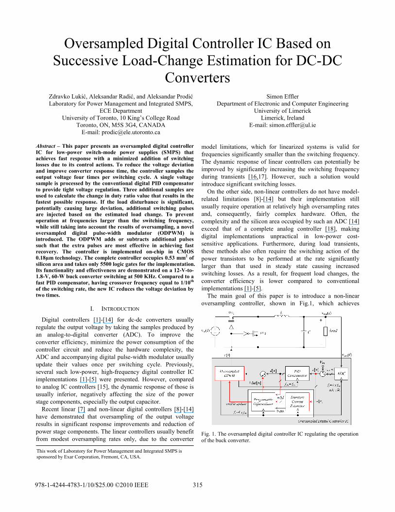
Fig. 1. The oversampled digital controller IC regulating the operation of the buck converter.
Oversampled Digital Controller IC Based on Successive Load-Change Estimation for DC-DC
Converters
Zdravko Lukić, Aleksandar Radić, and Aleksandar Prodić Laboratory for Power Management and Integrated SMPS,
ECE Department University of Toronto, 10 King’s College Road
Toronto, ON, M5S 3G4, CANADA E-mail: [email protected]
Simon Effler Department of Electronic and Computer Engineering
University of Limerick Limerick, Ireland
E-mail: [email protected]
Abstract – This paper presents an oversampled digital controller IC for low-power switch-mode power supplies (SMPS) that achieves fast response with a minimized addition of switching losses due to its control actions. To reduce the voltage deviation and improve converter response time, the controller samples the output voltage four times per switching cycle. A single voltage sample is processed by the conventional digital PID compensator to provide tight voltage regulation. Three additional samples are used to calculate the change in duty ratio value that results in the fastest possible response. If the load disturbance is significant, potentially causing large deviation, additional switching pulses are injected based on the estimated load change. To prevent operation at frequencies larger than the switching frequency, while still taking into account the results of oversampling, a novel oversampled digital pulse-width modulator (ODPWM) is introduced. The ODPWM adds or subtracts additional pulses such that the extra pulses are most effective in achieving fast recovery. The controller is implemented on-chip in CMOS 0.18µm technology. The complete controller occupies 0.53 mm2 of silicon area and takes only 5500 logic gates for the implementation. Its functionality and effectiveness are demonstrated on a 12-V-to-1.8-V, 60-W buck converter switching at 500 KHz. Compared to a fast PID compensator, having crossover frequency equal to 1/10th of the switching rate, the new IC reduces the voltage deviation by two times.
I. INTRODUCTION
Digital controllers [1]-[14] for dc-dc converters usually regulate the output voltage by taking the samples produced by an analog-to-digital converter (ADC). To improve the converter efficiency, minimize the power consumption of the controller circuit and reduce the hardware complexity, the ADC and accompanying digital pulse-width modulator usually update their values once per switching cycle. Previously, several such low-power, high-frequency digital controller IC implementations [1]-[5] were presented. However, compared to analog IC controllers [15], the dynamic response of those is usually inferior, negatively affecting the size of the power stage components, especially the output capacitor.
Recent linear [7] and non-linear digital controllers [8]-[14] have demonstrated that oversampling of the output voltage results in significant response improvements and reduction of power stage components. The linear controllers usually benefit from modest oversampling rates only, due to the converter
model limitations, which for linearized systems is valid for frequencies significantly smaller than the switching frequency. The dynamic response of linear controllers can potentially be improved by significantly increasing the switching frequency during transients [16,17]. However, such a solution would introduce significant switching losses.
On the other side, non-linear controllers do not have model-related limitations [8]-[14] but their implementation still usually require operation at relatively high oversampling rates and, consequently, fairly complex hardware. Often, the complexity and the silicon area occupied by such an ADC [14] exceed that of a complete analog controller [18], making digital implementations unpractical in low-power cost-sensitive applications. Furthermore, during load transients, these methods also often require the switching action of the power transistors to be performed at the rate significantly larger than that used in steady state causing increased switching losses. As a result, for frequent load changes, the converter efficiency is lower compared to conventional implementations [1]-[5].
The main goal of this paper is to introduce a non-linear oversampling controller, shown in Fig.1, which achieves
This work of Laboratory for Power Management and Integrated SMPS is sponsored by Exar Corporation, Fremont, CA, USA.
978-1-4244-4783-1/10/$25.00 ©2010 IEEE 315

Fig. 3. Normalized converter losses versus the frequency of the switching actions for a typical industrial converter designed to operate at 500 kHz [19].
Fig. 2. The operation of the oversampled digital controller during transient: a) multiple control actions based on successive load-change estimation b) control actions are “glued” to limit switching activity during transients to 2fsw.
significant output voltage transient improvements compared to conventional PID based controllers [1]-[5] using a very modest increase in oversampling rate and the minimum number of additional switching actions of the power transistors. During transients, the controller estimates the change in the load current [10,13] and accordingly modifies the control action such that the calculated changes of the duty ratio are averaged and “glued” to the DPWM. As a result, the switching frequency is not increased, but yet the effect of oversampling is fully utilized.
In the following section the controller operation based on successive load-change estimation is explained. In Section III we address the practical implementation of the key controller blocks, in particular oversampled DPWM with glued logic, and present the controller IC. In the final section, experimental results obtained with a buck converter prototype verifying the controller’s operation are demonstrated.
II. PRINCIPLE OF OPERATION
Figures 1 and 2 can be used for explaining how the control pulses in this controller are generated. To minimize the delays existing in once-per-cycle sampled systems [1]-[5], the oversampling controller of Fig.1 takes four samples of the output voltage errors signal e[n] during each switching cycle. Those four samples are processed by two functional blocks. The first block consists of Programmable Differentiator and a Transient Current Estimator (Fig.1). This block is active during transients only, to improve dynamic response. It takes all four error samples and, as shown in Fig.2.a), during output voltage deviations, produces Δd[n] values, corresponding to increase of the duty ratio control variable d[n]. The value Δd[n] is calculated with the programmable differentiator, which parameters are dynamically changed by the estimator. The estimator uses a modification of capacitor charge balance
algorithm [8]-[12] to estimate proper differentiator gain, ideally resulting in proximity time-optimal response.
The second block is a PID compensator that takes every 4th sample and by producing duty ratio control signal d[n] keeps system stable in steady-state conditions.
Ideally, during transients, this system could operate at the 4 times higher rate than the switching frequency to obtain a fast response. However, this implementation is not completely practical. As it can be seen from Fig.3, such an operation would incur additional switching losses and, for highly dynamic loads, significantly reduce the converter efficiency. Another practical problem is related to random quantization effects significantly affecting accuracy of Δd[n] calculations.
To solve for both of the previously mentioned problems sequence of Fig.2.a) is modified as shown in Fig.2.b). Instead of producing Δd[n] pulses at the 4 times the switching rate they
316

Fig. 4. Switching waveforms generated by the ODPWM for different duty ratio values.
are created every other switching cycle, while still the information about the calculated values is maintained. To minimize the random error effect, the average value of several pulses is calculated and their average value produced every other sampling cycle. At the sampling instants where the Δd[n] pulses coincide with those produced by the PID compensator, the increments are “glued” to the created pulse-width modulated signals. In this way, the switching rate of the system during transient is reduced to 2fsw, where fsw is the nominal frequency of the converter, reserved for the steady state operation.
The created pulses are sent to an oversampled digital pulse-width modulator (ODPWM). The ODPWM provides updates of the calculated values at the twice switching frequency. The ODPWM actively monitors the switching pulses of Fig.2.a), and, accordingly, readjusts their relative position to reduce the effective switching frequency, as shown in Fig.2.b). Its operation is described in the following section.
III. PRACTICAL IMPLEMENTATION
A. Oversampled DPWM To resolve the problem of frequent switching actions, shown
in Fig. 2.a), and reduce power stage switching losses during transients, the ODPWM attaches the oversampled pulses, such that the effect of the oversampling calculations is maximized
without a significant increase of switching frequency. The principle of operation is illustrated in Fig. 4 and can be
explained through the following example. For PID-calculated duty ratio values less than 0.25, additional pulses Δd1 and Δd2 are merged at the middle of the switching period while Δd3 is appended to the rising edge of the next generated PID pulse. If Δd1 and Δd2 are significantly large such that they extend beyond ¾Tsw, Δd3 is merged with the falling edge of Δd2 in order to reduce the delay of the control action and improve the response. Therefore the effective switching frequency is limited to 2fsw. A similar approach is used for duty ratios above 0.25. The only difference is that negative oversampled −Δd pulses can be now generated by subtracting them from the original pulse. This is beneficial for minimizing the voltage deviation during heavy-to-light load steps.
From Fig. 4, it can be observed that the ODPWM, while reducing the effective switching frequency, also minimizes the control action delay. This reduction in control delay contributes significantly to the reduction in output voltage deviation.
B. Conditions for Transient Operation Modern power converters [20,21] usually have a substantial
output voltage ripple due to the output capacitor ESR and the small inductance necessary for fast transient response. To appropriately react to load disturbances, the required ADC quantization step is small, typically in the range of a few millivolts [11-12,14]. This is several orders of magnitude smaller than the steady-state output voltage ripple [7]. To make the controller insensitive to the sampled voltage ripple, a trivial solution would be to increase the ADC quantization step above the ripple magnitude. The penalty of the increased quantization step is a slower transient response. Alternatively, ripple-compensation techniques [7] may be utilized at the price of more complex controller hardware. To resolve this problem in a simple manner, threshold conditions for transient operation with a small ADC quantization step are introduced and derived here.
To prevent the triggering of the system by small high-frequency variations of the load current and output voltage ripple, minimum injected pulse-width thresholds of the oversampling controller are calculated based on the worst-case steady-state ripple. In order to make these thresholds robust, both the capacitor ESR and the inductor current ripple are taken into account during this analysis. The change in the output voltage in steady-state is given by:
(1)
where Resr is the capacitor ESR value. From (1) it is clear that the maximum/minimum output voltage rates of change, causing maximum Δe, occur when the capacitor current is maximum/minimum and is given by:
(2)
,1c
Lesr
out iCdt
diRdt
dv ⋅+⋅=
,max errorq
sampleout
QV
Tdt
dv
e +⋅−
=Δ
317

Fig. 5. The oversampled controller IC: a) chip die photo b) mixed-signal simulation for a load step of 30 A with a buck converter switching at 500 KHz and having inductor and capacitor values of L=325 nH and C=600 µF.
where Qerror is the maximum quantization error due to the ADC sampling (Qerror = 1). Therefore the minimum injected duty value thresholds then become:
(3) where coefficients c1 and c2 are calculated based on the charge-balance principle [8]-[12] and the rising/falling inductor current slope respectively [22]. On the other hand, in order to reject the influence of large noise, the above analysis can be repeated to determine the maximum ±Δdmax threshold values. The value of ±Δdmax is obtained from the sum of the maximum load step and the inductor current ripple value, which is simply substituted into (1) in place of ic. If the rate of change of the load step is known it can also be included in the analysis; however, it may be beneficial to assume it is zero such that the initial output voltage drop due to Resr is also filtered out. The values of the ±Δdmin and ±Δdmax thresholds calculated by (3) are set within the programmable differentiator.
C. IC Implementation The controller architecture from Fig. 1 is fabricated on-chip
in CMOS 0.18µm technology and the chip die is shown in Fig. 5.a). A summary of the key IC parameters is provided in Table I. The controller occupies 0.53 mm2 of active silicon area. The digital portion of the controller is implemented in Verilog HDL and after synthesis it consists of 5500 logic gates. The operation of the controller is verified with a mixed-signal simulation. For a 30-A light-to-heavy load step, the results are shown in Fig. 5.b) where a 90 mV output voltage deviation and 6 µs settling time are observed. As it can be seen in Fig. 5.b), to minimize switching activity and improve efficiency, the
additional pulses are effectively “glued” while they are produced only until the voltage deviation is suppressed.
TABLE I. OVERSAMPLING CONTROLLER CHIP SUMMARY
Technology TSMC 0.18µm CMOS Supply voltage 1.8 V / 3.3 V ODPWM resolution 8 bits ODPWM nominal frequency 500 KHz ADC resolution 4 mV ADC sampling frequency 2 MHz ADC conversion time 300 ns Controller complexity 5500 gates Controller area (digital part) 0.31 mm2 ADC area 0.22 mm2 Total active chip area 0.53 mm2
IV. EXPERIMENTAL SYSTEM AND RESULTS
An experimental system verifying the operation of the oversampled controller IC was built based on the diagram shown in Fig. 1. The power stage is a 60-W, 12-V-to-1.8-V buck converter switching at 500 KHz. The inductor value L is 325 nH and the output capacitor value C is 600 µF. The on-chip ADC has a 4 mV resolution and a 300 ns conversion time. The PID compensator coefficients are externally programmed onto the chip to obtain a bandwidth higher than 1/10th of the switching frequency. Initially, controller blocks responsible for the non-linear operation are disabled and controller response is verified.
,2/1maxmin ced ⋅Δ±=Δ
318

Fig.6. The controller response to a 30-A load step with a) Conventional controller (left) b) Oversampled controller IC (right) – Ch1: Output converter voltage (100mV/div); Ch2: actual inductor current iL(t) ; D1- switching control signal, D0- load step command. Time scale is 5μs/div.
Fig. 6.a) shows the obtained response with a load step of 30 A with the PID compensator only. Even though the PID compensator reacts aggressively, increasing the inductor current to a value near the load step in one control action, due to the one cycle delay the voltage deviation is large and equal to 200 mV. The settling time is around 20 µs.
In the next step, the non-linear parts of the controller are enabled and the obtained controller response with the identical load step is tested as shown in Fig. 6.b). In this case, as soon as the load step is detected, by taking three additional samples, Δd pulse values are calculated by the programmable differentiator block. To minimize the number of switching actions and improve the converter efficiency the ODPWM attaches the pulses as described previously. As a result, only one additional switching sequence is added as shown in Fig. 6.b). Fig. 6.b) demonstrates also that the additional pulses are injected only until the initial voltage deviation is stopped, i.e. the inductor current has reached approximately the output load current. Therefore, during most of the settling period and in steady-state the converter switches at the nominal 500 KHz. The obtained voltage deviation is reduced by a factor of two (50%) compared to the PID compensator only and is 100 mV. The settling time is reduced to approximately 10 µs.
V. CONCLUSION
A practical oversampling digital controller IC for dc-dc converter is presented. The controller operates at a modest 4x oversampling rate. The controller utilizes parallel processing of error signal, where a PID compensator and a programmable differentiator are combined to provide stable operation and fast transient response. To minimize the switching losses transients and quantization effect while maintaining all advantages of the oversampling, “glue logic” and application specific oversampling digital pulse-width modulator are introduced.
Also, conditions for eliminating the unintentional triggering of the controller, due to capacitor voltage ripple are derived. The effectiveness of the IC is verified on an experimental
system, demonstrating fast transient response and stable operation in all operating conditions.
REFERENCES [1] B. Patella, A. Prodić, A. Zirger and D. Maksimović, “High-frequency
digital PWM controller IC for DC/DC converters,” IEEE Transactions on Power Electronics, Special Issue on Digital Control, Jan. 2003, Vol.18, Issue1, pp. 438-446.
[2] J.Xiao, A.V. Peterchev, J. Zhang, and S.R. Sanders, “A 4-μA quiescent-current dual-mode digitally controlled buck converter IC for cellular phone applications,” IEEE Journal of Solid-State Circuits, vol. 39, pp. 2342–2348, Dec. 2004.
[3] A.V. Peterchev, J. Xiao and S.R. Sanders, “Architecture and implementation of a digital VRM controller,” IEEE Transactions on Power Electronics, vol.18, issue 1, pp. 356 – 364, Jan. 2003.
[4] Z. Lukić, N. Rahman, and A. Prodić, “Multi-bit Σ-∆ PWM digital controller IC for DC–DC converters operating at switching frequencies beyond 10 MHz,” IEEE Trans. Power Electron., vol. 22, pp. 1693-1707, Sept. 2007.
[5] A. Parayandeh, and A. Prodić, “Programmable analog-to-digital converter for low-power DC-DC SMPS,” IEEE Trans. Power Electron., vol. 23, pp. 1719-1730, Jan. 2008.
[6] H. Hu, V. Yousefzadeh and D. D. Maksimović, “Nonuniform A/D quantization for improved dynamic responses of digitally controlled DC–DC converters,” IEEE Transactions on Power Electronics, vol.23, issue 4, pp. 1998 – 2005, Jul. 2008.
[7] L. Corradini, P. Mattavelli, E. Tedeschi, D. Trevisan, “High-bandwidth multisampled digitally controlled DC–DC converters using ripple compensation,” IEEE Trans. Industrial Electron., Volume 55, Issue 4, April 2008, pp. 1501 - 1508.
[8] G. Feng, E. Meyer, and Y.-F. Liu, “A new digital control algorithm to achieve optimal dynamic performance in DC-to-DC converters,” IEEE Trans. Power Electron., vol. 22, pp. 1489–1498, July 2007.
[9] Z. Zhao, and A. Prodić , "Continuous-time digital controller for high-frequency DC-DC converters," IEEE Trans. Power Electron., vol. 23, pp. 564-573, May 2008.
[10] V. Yousefzadeh, A. Babazadeh, B. Ramachandran, E. Alarcon, L. Pao, and D. Maksimović, “Proximate time-optimal digital control for synchronous buck DC-to-DC converters,” IEEE Trans. Power Electron., Volume 22, Issue 4, Jul. 2007, pp. 1489 – 1498.
[11] A. Costabeber, L. Corradini, P. Mattavelli, and S. Saggini, “Time optimal, parameters-insensitive digital controller for DC-DC buck converters,” in Proc. IEEE Power Electronics Specialist Conf., 2008, pp. 1243–1249.
[12] L. Corradini, A. Costabeber, P. Mattavelli, and S. Saggini, “Time optimal, parameters-insensitive digital controller for VRM applications with adaptive voltage positioning,” in Proc. IEEE Workshop on Computers in Power Elecronics, 2008, pp. 1–8.
319

[13] S. Effler, A. Kelly, M. Halton, T. Kruger, and K. Rinne, “Digital control law using a novel load current estimator principle for improved transient response,” in Proc. IEEE Power Electronics Specialist Conf., 2008, pp. 4585–4589.
[14] L. Corradini, E. Orietti, P. Mattavelli, and S. Saggini, “Digital hysteretic voltage-mode control for DC-DC converters based on asynchronous sampling,” IEEE Trans. Power Electron., vol. 24, pp. 201–211, Jan. 2009.
[15] “A voltage regulator module (VRM) using the HIP6004 PWM controller application note,” Intersil Corp, Milpitas, USA.
[16] Xiaoming Duan, A. Q. Huang, “Current-mode variable-frequency control architecture for high-current low-voltage DC-DC converters,” IEEE Transactions on Power Electronics, July 2006, Vol.21, Issue1 4, pp. 1133-1137.
[17] Lilly Kumar, M. Pavan , “Variable switching frequency voltage regulator to optimize power loss”, US Patent 6639391.
[18] Kuo-Hsing Cheng, Chia-Wei Su, and Hsin-Hsin Ko, “A high-accuracy and high-efficiency on-chip current sensing for current-mode control CMOS DC-DC buck converter”, IEEE 15th International Electronics, Circuits and Systems Conference, 2008, pp. 458-461.
[19] “AN9672 - PIP212-12M Design Guide application note,” NXP Semiconductors, Eindhoven, Netherlands.
[20] “PIP212-12M data sheet,” NXP Semiconductors, Eindhoven, Netherlands.
[21] “FDMF8700 data sheet,” Fairchild Semiconductors, San Jose, USA. [22] R. W. Erickson and D. Maksimovic, Fundamentals of Power Electronics.
New York, NY:Springer Sience+Business Media Inc., 2001.
320