Analysis, Design, and Experimentation on Constant-Frequency DC-DC Resonant Converters With Magnetic...
14
IEEE TRANSACTIONS ON POWER ELECTRONICS, VOL. 27, NO. 3, MARCH 2012 1369 Analysis, Design, and Experimentation on Constant-Frequency DC-DC Resonant Converters With Magnetic Control J. Marcos Alonso, Senior Member, IEEE, Marina S. Perdig˜ ao, Student Member, IEEE, David Gacio Vaquero, Student Member, IEEE, Antonio J. Calleja, Member, IEEE, and Eduardo Sousa Saraiva, Member, IEEE Abstract—In this paper, a new technique for controlling dc-dc resonant converters is investigated. A variable inductance is used to control and regulate the dc output voltage maintaining constant switching frequency for the half-bridge transistors. The output voltage characteristics of the series resonant and parallel resonant converters under the proposed magnetic control are obtained and analyzed. In order to evaluate the proposed technique, a labora- tory prototype for a 48 V-input 5 V/10 A-output 500 kHz parallel resonant converter is presented. A methodology for obtaining the converter dynamic response using a step response test is carried out. From the dynamic response, a compensator for operating the converter at closed loop is developed and tested in the laboratory. The results prove that the proposed technique is suitable for con- troling resonant inverters at constant frequency using a low-cost half-bridge inverter. Index Terms—Closed loop operation, constant switching fre- quency, dc-dc converters, low EMI, magnetic control, magnetic regulator, resonant conversion, variable inductance. I. INTRODUCTION D C-DC converters are used in many applications including telecommunications, battery chargers, fuel cells, ultraca- pacitors, electric vehicles, etc. [1]–[16]. DC-DC resonant con- verters were introduced in an effort to reduce switching losses, and in turn boost the operating frequency ultimately achieving a lower profile, a major requirement of today’s appliances. Typ- ical modes of operation are: 1) zero voltage switching (ZVS) at turn-ON, where the switches do not present losses during the turn-ON process but do during the turning OFF, and 2) zero cur- Manuscript received April 1, 2011; revised June 22, 2011; accepted July 30, 2011. Date of current version February 7, 2012. This work was supported in part by the Spanish Government, Education and Science Office, under research grants DPI2007-61267 and DPI2010-15889 and in part by the Government of the Portuguese Republic, FCT-MCTES, under research grants PTDC/EEA- ENE/66859/2006 and SFRH/BD/36143/2007. Recommended for publication by Associate Editor S. Williamson. J. M. Alonso, D. G. Vaquero, and A. J. Calleja are with the Universidad de Oviedo, Electrical and Electronics Engineering Department, 33204-Gij´ on, Asturias, Spain (e-mail: [email protected]). M. S. Perdig˜ ao is with the Instituto de Telecomunicac ¸˜ oes, P ´ olo II, 3030-290, Coimbra, Portugal. She is also with the DEE, ISEC, IPC, R. Pedro Nunes, 3030-199 Coimbra, Portugal. E. S. Saraiva is with the DEEC, University of Coimbra, Portugal. He is also with the Instituto de Telecomunicac ¸˜ oes, P´ olo II, 3030-290, Coimbra, Portugal, and with the DEE, ISEC, IPC, R. Pedro Nunes, 3030-199 Coimbra, Portugal. Color versions of one or more of the figures in this paper are available online at http://ieeexplore.ieee.org. Digital Object Identifier 10.1109/TPEL.2011.2165083 rent switching (ZCS) at turn-OFF, where the losses are negligible during the turn-OFF process but are still present during turning ON [17]. Resonant converters usually employ the switching frequency as a control parameter to regulate the output voltage. Changes in the operating frequency vary the impedances of the reactive elements used in the resonant tank, so that the output voltage is modified. In some cases, depending on the input-output voltage ratio and the power handled by the resonant tank, the frequency excursion can be high. This complicates the design and construc- tion of the EMI filter used to avoid electromagnetic interference with other equipment, which today is a basic requirement be- cause of the high number of electronic equipment operating simultaneously in a particular installation. Moreover, the EMI filter needs to be designed for the lowest frequency of opera- tion, which in many cases coincides with the maximum power handled by the converter [18]. This is the case, for example, with the parallel resonant converter operating above resonant frequency in ZVS mode. In order to avoid variable frequency operation in dc-dc reso- nant converters, several approaches have been proposed in the literature. The most common one makes use of a full-bridge inverter with phase-shift control, where the gate signals of each branch are shifted in time to obtain a quasisquare output voltage waveform with adjustable rms value [19]. This solution can also be implemented by coupling two inverters in series using an output transformer. However, this solution requires some extra components, power switches, transformers and associated con- trol, and driving circuitry, making it costly and not appropriate for many cost-conscious applications. Another possibility is the use of a two-stage configuration in which the first stage is used to modify the input voltage to the second stage [20], [21]. The main drawbacks of this solution are the higher cost and the lower efficiency as a result of the two-stage configuration. In this paper, an alternative solution to implement a single- stage two-switch constant-frequency dc-dc resonant converter is presented. The new approach is based on the use of a variable in- ductance to include an additional control parameter, namely the converter resonant inductance. Variable inductors have exten- sively been used in power applications in recent years [22]–[30], [32] and provide a means to changing the inductance that ex- ists in a resonant tank by using a dc-control current circulating through an additional winding. In Section II, the magnetic con- trol is introduced and the characteristics of two basic dc-dc 0885-8993/$26.00 © 2011 IEEE
-
Upload
independent -
Category
Documents
-
view
4 -
download
0
Transcript of Analysis, Design, and Experimentation on Constant-Frequency DC-DC Resonant Converters With Magnetic...

IEEE TRANSACTIONS ON POWER ELECTRONICS, VOL. 27, NO. 3, MARCH 2012 1369
Analysis, Design, and Experimentation onConstant-Frequency DC-DC Resonant
Converters With Magnetic ControlJ. Marcos Alonso, Senior Member, IEEE, Marina S. Perdigao, Student Member, IEEE,
David Gacio Vaquero, Student Member, IEEE, Antonio J. Calleja, Member, IEEE,and Eduardo Sousa Saraiva, Member, IEEE
Abstract—In this paper, a new technique for controlling dc-dcresonant converters is investigated. A variable inductance is usedto control and regulate the dc output voltage maintaining constantswitching frequency for the half-bridge transistors. The outputvoltage characteristics of the series resonant and parallel resonantconverters under the proposed magnetic control are obtained andanalyzed. In order to evaluate the proposed technique, a labora-tory prototype for a 48 V-input 5 V/10 A-output 500 kHz parallelresonant converter is presented. A methodology for obtaining theconverter dynamic response using a step response test is carriedout. From the dynamic response, a compensator for operating theconverter at closed loop is developed and tested in the laboratory.The results prove that the proposed technique is suitable for con-troling resonant inverters at constant frequency using a low-costhalf-bridge inverter.
Index Terms—Closed loop operation, constant switching fre-quency, dc-dc converters, low EMI, magnetic control, magneticregulator, resonant conversion, variable inductance.
I. INTRODUCTION
DC-DC converters are used in many applications includingtelecommunications, battery chargers, fuel cells, ultraca-
pacitors, electric vehicles, etc. [1]–[16]. DC-DC resonant con-verters were introduced in an effort to reduce switching losses,and in turn boost the operating frequency ultimately achievinga lower profile, a major requirement of today’s appliances. Typ-ical modes of operation are: 1) zero voltage switching (ZVS)at turn-ON, where the switches do not present losses during theturn-ON process but do during the turning OFF, and 2) zero cur-
Manuscript received April 1, 2011; revised June 22, 2011; accepted July 30,2011. Date of current version February 7, 2012. This work was supported inpart by the Spanish Government, Education and Science Office, under researchgrants DPI2007-61267 and DPI2010-15889 and in part by the Governmentof the Portuguese Republic, FCT-MCTES, under research grants PTDC/EEA-ENE/66859/2006 and SFRH/BD/36143/2007. Recommended for publicationby Associate Editor S. Williamson.
J. M. Alonso, D. G. Vaquero, and A. J. Calleja are with the Universidadde Oviedo, Electrical and Electronics Engineering Department, 33204-Gijon,Asturias, Spain (e-mail: [email protected]).
M. S. Perdigao is with the Instituto de Telecomunicacoes, Polo II, 3030-290,Coimbra, Portugal. She is also with the DEE, ISEC, IPC, R. Pedro Nunes,3030-199 Coimbra, Portugal.
E. S. Saraiva is with the DEEC, University of Coimbra, Portugal. He is alsowith the Instituto de Telecomunicacoes, Polo II, 3030-290, Coimbra, Portugal,and with the DEE, ISEC, IPC, R. Pedro Nunes, 3030-199 Coimbra, Portugal.
Color versions of one or more of the figures in this paper are available onlineat http://ieeexplore.ieee.org.
Digital Object Identifier 10.1109/TPEL.2011.2165083
rent switching (ZCS) at turn-OFF, where the losses are negligibleduring the turn-OFF process but are still present during turningON [17].
Resonant converters usually employ the switching frequencyas a control parameter to regulate the output voltage. Changesin the operating frequency vary the impedances of the reactiveelements used in the resonant tank, so that the output voltage ismodified. In some cases, depending on the input-output voltageratio and the power handled by the resonant tank, the frequencyexcursion can be high. This complicates the design and construc-tion of the EMI filter used to avoid electromagnetic interferencewith other equipment, which today is a basic requirement be-cause of the high number of electronic equipment operatingsimultaneously in a particular installation. Moreover, the EMIfilter needs to be designed for the lowest frequency of opera-tion, which in many cases coincides with the maximum powerhandled by the converter [18]. This is the case, for example,with the parallel resonant converter operating above resonantfrequency in ZVS mode.
In order to avoid variable frequency operation in dc-dc reso-nant converters, several approaches have been proposed in theliterature. The most common one makes use of a full-bridgeinverter with phase-shift control, where the gate signals of eachbranch are shifted in time to obtain a quasisquare output voltagewaveform with adjustable rms value [19]. This solution can alsobe implemented by coupling two inverters in series using anoutput transformer. However, this solution requires some extracomponents, power switches, transformers and associated con-trol, and driving circuitry, making it costly and not appropriatefor many cost-conscious applications. Another possibility is theuse of a two-stage configuration in which the first stage is usedto modify the input voltage to the second stage [20], [21]. Themain drawbacks of this solution are the higher cost and the lowerefficiency as a result of the two-stage configuration.
In this paper, an alternative solution to implement a single-stage two-switch constant-frequency dc-dc resonant converter ispresented. The new approach is based on the use of a variable in-ductance to include an additional control parameter, namely theconverter resonant inductance. Variable inductors have exten-sively been used in power applications in recent years [22]–[30],[32] and provide a means to changing the inductance that ex-ists in a resonant tank by using a dc-control current circulatingthrough an additional winding. In Section II, the magnetic con-trol is introduced and the characteristics of two basic dc-dc
0885-8993/$26.00 © 2011 IEEE

1370 IEEE TRANSACTIONS ON POWER ELECTRONICS, VOL. 27, NO. 3, MARCH 2012
Fig. 1. Proposed constant frequency dc-dc resonant converter.
Fig. 2. Basic dc-dc converters with magnetic control. (a) Series resonant tank.(b) Parallel resonant tank.
resonant converters are presented. In Section III, the design andimplementation of the laboratory prototype is shown. Experi-mental results are provided in Section IV. Finally, the paper isconcluded in Section V.
II. MAGNETIC CONTROL OF DC-DC RESONANT CONVERTERS
Fig. 1 illustrates the block diagram of the proposed converter.The basic structure is similar to any dc-dc resonant converter.What differs is that the proposed converter uses a variable in-ductance in the resonant tank circuit. The variable inductanceis controlled by means of a dc current that makes it possible tochange the effective inductance value by taking certain parts ofthe magnetic core to a close-to-saturation region. The effectivemagnetic reluctance of the arrangement is, therefore, increasedresulting in a lower value for the inductance [25].
Fig. 2 shows the two most common resonant inverters inwhich this technique could be applied. Fig. 2(a) shows the seriesresonant converter (SRC), which corresponds to a resonant tankin which the effective load (given by the arrangement rectifier,filter capacitor and load resistance) is connected in series withthe resonant elements.
In Fig. 2(b) the parallel resonant converter (PRC) is shown.Even though this converter makes use of a series resonance
Fig. 3. Equivalent circuit of the dc-dc series resonant converter.
between the inductance and the capacitance, it is usually referredto as a parallel resonant converter because, in this case, theeffective load of the resonant tank is connected in parallel withthe resonant capacitor [31].
A. Analysis of the DC-DC Series Resonant Converterwith Magnetic Control
It is well known that the series resonant converter can bemodeled with the circuit shown in Fig. 3 [31]. The voltagesource V1 represents the fundamental component of the squarewaveform generated by the half-bridge transistors. The peakvalue of V1 is given by
V1 =4VCC/2
π=
2VCC
π. (1)
The converter net load formed by the rectifier, filter and loadcan be modeled as an effective resistance, RES , with its valuegiven by [31]
RES =8π2 R (2)
where R is the converter load resistance.In this way, it is simple to calculate the current passing through
the resonant tank
IRE S =V1
RES + jωL − j(1/ωCS )
=V1
(8R/π2) + jωL − j(1/ωCS )(3)
where ω is the angular frequency of the input voltage ω = 2πf .This current is rectified and then filtered by the output capaci-tance, CO . Thus, the dc output voltage VOS will be given by therectified mean output current multiplied by the load resistance.This is
VOS =2||IRE S ||
πR
=2V1
π
1√
(8/π2)2 + (1/R2)(ωL − (1/ωCS ))2. (4)
Using (4), the dc output voltage can be plotted for different loadresistances as a function of the resonant inductance, which is thecontrol parameter in the proposed technique. Fig. 4 illustratesthe output voltage characteristics of the series resonant converterwith magnetic control.

ALONSO et al.: ANALYSIS, DESIGN, AND EXPERIMENTATION ON CONSTANT-FREQUENCY DC-DC RESONANT CONVERTERS 1371
Fig. 4. Output voltage characteristics of the series resonant converter withmagnetic control.
Fig. 5. Equivalent circuit of the dc-dc parallel resonant converter.
As can be seen in Fig. 4, in the case of the series resonantinverter, a high inductance excursion might be necessary if theconverter must operate with very light loads. In fact, for no loadoperation, the required inductance value would be infinite in theideal case. This effect may limit the use of this type of converterin applications in which a wide load range is required.
B. Analysis of the DC-DC Parallel Resonant Converter withMagnetic Control
Fig. 5 illustrates the equivalent circuit of the dc-dc parallelresonant converter. It is well known that for this converter, theeffective load given by the rectifier, filter, and load resistance isgiven by the following expression [31]
REP =π2
8R. (5)
The voltage across the effective resistance can then be easilycalculated by
VRE P = V1−(jREP/ωCP )
(L/CP ) + jREP(ωL − (1/ωCP )). (6)
This voltage is rectified and filtered, so that the dc outputvoltage applied to the converter load is equal to the rectifiedmean voltage, which can be calculated as follows
VO =2||VRE P ||
π=
2V1
π
(REP/ωCP )√
(L/CP )2 + E2EP(ωL − (1/ωCP ))2
.
(7)
Fig. 6. Output voltage characteristics of a parallel resonant converter withmagnetic control.
Using (5) in (7), the following expression is obtained for thedc output voltage
VO =2V1
π
1√
((8/π2R)ωL)2 + 1(1 − ω2LCP )2. (8)
Fig. 6 illustrates the dc output voltage characteristic of the par-allel resonant converter obtained by plotting (8). As can be seen,in the case of the parallel converter, it is possible to attain op-eration from full load to open load maintaining a reasonableexcursion of the resonant inductance. Therefore, this topologywould be ideal for applications in which operation at light loadsis required.
III. LABORATORY PROTOTYPE
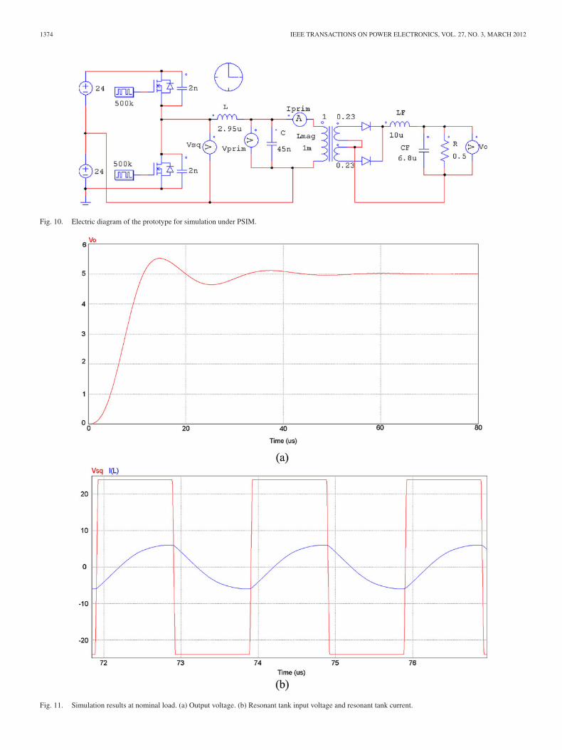
In order to test the possibilities of the dc-dc resonant convert-ers with magnetic control, an experimental prototype has beendeveloped. The prototype has been designed to operate witha 48 V input voltage and a 5 V output voltage. The maximumoutput current is 10 A. Switching frequency has been selectedto be 500 kHz. The complete electric diagram of the prototypecan be seen in Fig. 7. A step-down transformer is used betweenthe resonant capacitor and the output rectifier to achieve thenecessary step-down ratio.
A. Resonant Tank
The first step for designing the converter is the selection ofthe transformer turns ratio. In this prototype, the transformer isdesigned so that the resonant tank operates with an input-outputvoltage ratio close to unity. This gives the following value forthe transformer secondary to primary turns ratio
n =πVO /22VCC/π
=π2VO
4VCC(9)
where VO is the dc output voltage and VCC is the total dc inputvoltage that supplies the converter. Using the values previouslymentioned, a turns ratio n = 0.26 is obtained. The transformerwas implemented using an EFD20 core with N87 magneticmaterial, with nine turns in the primary side and two turns ineach secondary winding. This gives a final turns ratio of n =0.23. Additional details are shown in Table I.

1372 IEEE TRANSACTIONS ON POWER ELECTRONICS, VOL. 27, NO. 3, MARCH 2012
Fig. 7. Closed loop diagram of the dc-dc resonant converter with magnetic control.
TABLE IEXPERIMENTAL PROTOTYPE MATERIAL LIST
Once the turns ratio has been obtained, it is possible to calcu-late the effective load resistance of the resonant tank transferredto the primary side
REP =π2R
8n2 . (10)
Using the values for the present prototype R = 0.5 Ω andn = 0.23, in (10), a value REP = 11.7 Ω is obtained.
The output voltage can be calculated as a function of theinductance by using (8) and taking into account the transformerturns ratio, as follows:
VO =2nV1
π
1√
((8n2/π2R)ωL)2 + 1(1 − ω2LCP )2. (11)
Fig. 8. Inductance as a function of load resistance for different values of tankcapacitance.
Solving (11) for the inductance L, the necessary inductancefor a given output voltage and load resistance is obtained asshown in (12), at the bottom of this page.
There are two solutions corresponding to the operation belowand above resonance. In this prototype, operation above reso-nance is preferred so that ZVS can be achieved. Thus, Fig. 8illustrates the inductance as a function of the load resistance fordifferent values of the resonant tank capacitance, obtained byplotting (12). It is seen how for high values of the load resistance,the inductance remains nearly constant because the operation isclose to the no load condition. It can also be seen how, as long asthe capacitance decreases, the inductance excursion increases.Thus, in order to avoid an excessive inductance excursion, a ca-pacitance CP = 45 nF has been selected for this prototype.
L =2ω2CP ±
√(2ω2CP )2 − 4[(8n2ω/π2R)2 + (ω2CP )2 ][1 − (2nV1/πVO )2 ]
2[(8n2ω/π2R)2 + (ω2CP )2 ]. (12)

ALONSO et al.: ANALYSIS, DESIGN, AND EXPERIMENTATION ON CONSTANT-FREQUENCY DC-DC RESONANT CONVERTERS 1373
Fig. 9. Output voltage characteristics of the designed prototype.
Therefore, the inductance will vary between approximately3 μH and 4.3 μH. In order to check these results, Fig. 9 il-lustrates the output voltage characteristics obtained by plotting(11) for the nominal input voltage. As can be seen, operationfrom no load to nominal load is achieved.
To conclude the design, the values of the output filter induc-tance and capacitance must be obtained. These components areused to filter the rectified sinusoidal output voltage. The de-sign of these components follows the typical methodology fora low pass filter, given the inductance current ripple and theoutput voltage ripple. In this case, the calculated values wereL = 10μH and C = 6.8 μF.
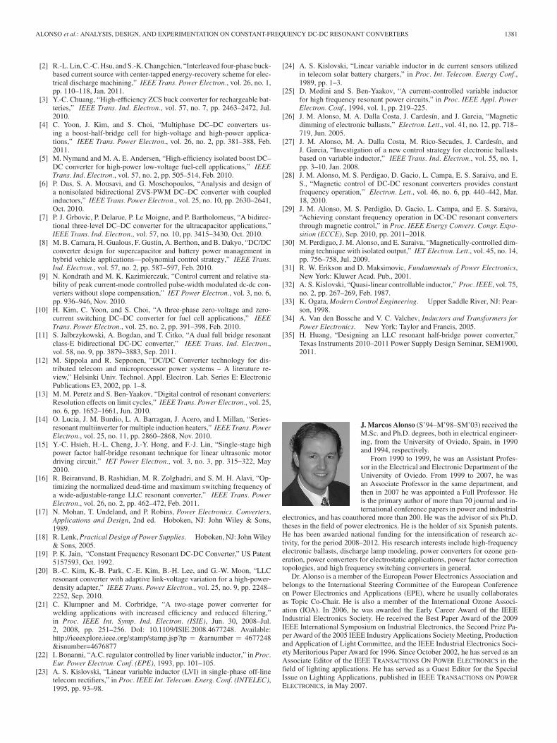
In order to check the design, a simulation was carried outusing the PSIM simulator. Fig. 10 illustrates the circuit usedfor the simulation. The results are shown in Figs. 11 and 12.As can be seen, the output voltage reaches the nominal levelof approximately 5.0 V in 50 μs. The peak inductance currentis around 6.0 A and the transformer primary current is a squarewaveform with a peak value of 2.32 A. All simulation resultsare in good agreement with the theoretical design.
B. Variable Inductor
An EFD25 core with N87 material by Siemens was selectedto implement the variable inductor. It was built following thestructure shown in Fig. 13(a) [25]–[30]. The selected cores are0.3 mm gapped each, giving a total gap g = 0.6 mm. (Note thatthis selection was made based on laboratory availability. Othercores and especially other magnetic materials would surely bemore adequate, since the N87 material is in the limit for 500 kHzoperation.) Then, the inductance factor AL for this core can becalculated as follows:
AL =μ0Ae
g(13)
where μ0 is the vacuum permeability and Ae is the effective areaof the core. Using the values for the EFD25, an inductance factorequal to 121.5 nH is obtained. With this value it is possible tocalculate the number of turns necessary for a given inductance
N =√
L
AL. (14)
The inductor must be designed to operate at its maximum valuewhen no dc-bias current is injected through the control winding.This condition gives the number of turns necessary for the vari-able inductor. Then, with the calculated inductance factor andthe maximum inductance value, which in this case is 4.5 μH,and using (14), a number of turns equal to 6 is obtained.
The expected peak value of the flux density for the ac com-ponent can be calculated as follows:
B =NAL
AeI (15)
where I is the peak value of the ac current through the in-ductance. In the design, the peak current is nearly 6.0 A forthe nominal operating point. Employing (15), the calculatedac peak flux density is 75 mT. Using this value in the lossescharacteristics given by the manufacturer, the estimated loss pervolume is 400 kW/m3 . This means that the total loss for thecore set is 1.3 W. To this should be added the losses in the wind-ing. This calculation is not however obvious and is thereforeout of the scope of this paper. These losses will be evaluatedexperimentally as shown in next section. The control windingwas implemented using NDC = 65 turns and with a 0.15 mmdiameter wire.
Fig. 13(b) shows a photograph of the variable inductor. Themeasured inductance as a function of the dc control currentapplied through the control windings is illustrated in Fig. 14.As can be seen, an inductance variation from 3.0 to 4.5 μHis achieved with a maximum control current of 180 mA. Thiscurrent level is perfectly handled by a linear regulator withoutexcessive efficiency penalty.
The details of the laboratory prototype are shown in Table Iand the electric diagram of the prototype for open-loop operationis illustrated in Fig. 15.
C. Dynamic Response
The dynamic response of the laboratory prototype was ob-tained by means of a step-response test. For this, a dc voltagewith a 100 mV peak-to-peak superposed square waveform wasapplied to the control input shown in Fig. 15. The result is illus-trated in Fig. 16. From the obtained waveform, it is clear that thesystem follows a second-order response that can be expressedas
G(s) =vo(s)vc(s)
=kω2
n
s2 + 2ξωns + ω2n
(16)
where vo and vc are the small-signal perturbations of the out-put voltage and control voltage, respectively, and k, ξ, and ωn
are the dc gain, the damping factor and the angular frequencyof the response, respectively. These values can be calculatedfrom the waveforms shown in Fig. 16 using traditional controltheory [33], as shown in Appendix I. The values obtained forthe different parameters in (16) are shown in Table II. Usingthese parameters, the Bode diagram illustrated in Fig. 17 can berepresented.
In order to test the converter in closed loop, a compensatorbased on the electric diagram shown in Fig. 18 was designed.The dynamic response of the compensator can be expressed as
1374 IEEE TRANSACTIONS ON POWER ELECTRONICS, VOL. 27, NO. 3, MARCH 2012
Fig. 10. Electric diagram of the prototype for simulation under PSIM.
Fig. 11. Simulation results at nominal load. (a) Output voltage. (b) Resonant tank input voltage and resonant tank current.

ALONSO et al.: ANALYSIS, DESIGN, AND EXPERIMENTATION ON CONSTANT-FREQUENCY DC-DC RESONANT CONVERTERS 1375
Fig. 12. Simulation results at nominal load. (Top) Transformer primary voltage. (Bottom) current.
Fig. 13. Developed variable inductor. (a) Schematic diagram. (b) Photograph.
Fig. 14. Inductance value as a function of the dc control current.
follows:
C(s) = K1 + s/ωz
s(1 + s/ωp)(17)
where K = RA [R1C2(RA + RB )]−1 , ωz = (R2C2)−1 , ωp =(RpCA )−1 and RP = RA RB /(RA + RB ).
The compensator was designed using traditional techniques,obtaining the values for the constant K, and the zero and polefrequencies ωz and ωp, respectively. Capacitor CA is used toavoid high frequency noise at the input of the error amplifier.Therefore, the frequency of the pole is selected to be around1 kHz. The frequency of the zero is selected to compensate theeffect of the filter pole and it is placed around 10 kHz. In thismanner, the compensator behaves mainly as an integral action,thus making zero the steady state error. The exact parametersused in the compensator are shown in Table III. The Bode dia-gram of the compensator is illustrated in Fig. 19 and the systemopen-loop Bode diagram is shown in Fig. 20. With the valuesshown in Table III, a 75◦ phase margin is achieved. The obtainedgain margin was 24 dB and the 0 dB bandwidth was 350 Hz.Thus, the theoretical step response of the converter operatingin closed loop is illustrated in Fig. 21. As can be seen, an overdamped response is obtained with a settling time around 1 ms.
IV. EXPERIMENTAL RESULTS
Fig. 22 illustrates the complete electric diagram of the lab-oratory prototype, including the error amplifier circuit and thevoltage-controlled current source used to generate the dc controlcurrent for the variable inductance.
Fig. 23 shows the gate-to-source driving signals of the bridgetransistors. As can be seen, the operating frequency is 500 kHzwith a dead time of approximately 250 ns, which is used toassure ZVS operation.
Fig. 24 illustrates the waveforms at the input of the resonanttank, i.e., the square input voltage and the resonant current,for 48 V input voltage and 50 W output power. Note that thevoltage was measured using an isolated voltage probe with a5:1 attenuation. It can be observed a ZVS operation becausethe voltage transition is smooth with no voltage spikes. Agood agreement is found with the simulation results shown inFig. 11. Fig. 25 shows the voltage and current waveforms in the

1376 IEEE TRANSACTIONS ON POWER ELECTRONICS, VOL. 27, NO. 3, MARCH 2012
Fig. 15. Electric diagram of the prototype for open-loop operation.
Fig. 16. Experimental dynamic response of the laboratory prototype. (Bottom)Reference voltage step (1 V/div). (Top) Output voltage (200 mV/div). Horiz.scale: 500 μs/div.
TABLE IIPARAMETERS OF THE DYNAMIC RESPONSE OF THE LABORATORY PROTOTYPE
half-bridge low transistor. Fig. 26 illustrates the transformer in-put voltage and current. These waveforms also match quite wellthe theoretical analysis and the simulation results illustrated inFig. 12.
Fig. 17. Bode diagram of the open-loop control-to-output voltage response ofthe laboratory prototype.
TABLE IIIPARAMETERS OF THE COMPENSATOR
Fig. 18. Electric diagram of the compensator.

ALONSO et al.: ANALYSIS, DESIGN, AND EXPERIMENTATION ON CONSTANT-FREQUENCY DC-DC RESONANT CONVERTERS 1377
Fig. 19. Bode diagram of the compensator.
Fig. 20. Bode diagram of the system in open loop.
Fig. 27 shows the measured output voltage as a functionof the resonant inductance for several load resistances whenoperating at 48 V input voltage. The voltage response is as ex-pected from the theoretical analysis and demonstrates that theinductance can be used as a control parameter for the outputvoltage. It must be noted that in this figure, the normal oper-ation range for which the converter was designed goes fromapproximately 3 to 4.5 μH. This can be seen by the fact that the5 V output for the 0.5 Ω load is achieved for an inductance ofnearly 3 μH. This point represents the full load operating point.The rest of the data represented out of the normal operationpoint were measured in order to check the static response of theconverter.
The closed-loop operation results are illustrated in Fig. 28. Ascan be seen, a good voltage regulation is achieved as long as thereis margin for the dc control current to control the inductance.The regulation is limited in the higher input voltage range by
Fig. 21. Step response of the converter in closed loop operation.

1378 IEEE TRANSACTIONS ON POWER ELECTRONICS, VOL. 27, NO. 3, MARCH 2012
Fig. 22. Schematic diagram of the complete prototype.
Fig. 23. Gate-to-source voltage in the bridge transistors illustrating the deadtime between the two driving signals. 5 V/div, 500 ns/div.
the dc control current reaching zero and in the lower range bythe ZVS-ZCS boundary. When ZCS is reached, the switchinglosses of the bridge transistors increase greatly, mainly due tothe poor behavior or the MOSFETs body diodes. This reducesefficiency and could even destroy the switches due to excessive
Fig. 24. Resonant tank waveforms: input voltage, input current and inputpower (top). 25 V/div, 10 A/div, 500 ns/div.
junction temperature. Therefore, operation in this region wasavoided.
Fig. 29(a) shows the experimental results for a load step from5 to 10 A. The converter output voltage and the compensator

ALONSO et al.: ANALYSIS, DESIGN, AND EXPERIMENTATION ON CONSTANT-FREQUENCY DC-DC RESONANT CONVERTERS 1379
Fig. 25. Current and voltage waveforms in the half-bridge low transistor.20 V/div, 5 A/div, 500 ns/div.
Fig. 26. Transformer input voltage and current at nominal operation. 20 V/div,5 A/div, 1 μs/div.
output voltage are shown. Similarly, Fig. 29(b) shows the samewaveforms for a load step from 10 to 5 A. As can be seen, inboth tests, the output voltage is compensated in around 1 ms,which is in good agreement with the theoretical design.
One of the main drawbacks of the developed prototype wasfound in the low efficiency attained, which reached a max-imum of only 82% at full load (48 V input, 5 V-10 A out-put). Even though synchronous rectification was implementedusing IRFZ48 transistors, the efficiency was not improvedsignificantly.
In order to investigate the low efficiency attained, the lossesin the variable inductor were measured using the oscilloscopemethod [34]. This is not the most accurate method for measur-ing inductor losses but it is admissible in this case in order to
Fig. 27. Experimental results for open-loop operation at 48 V input voltage.Measured dc output voltage as a function of the variable inductance for differentloads.
Fig. 28. Experimental results for closed-loop operation. Measured output volt-age and inductance control current as a function of the dc input voltage.
TABLE IVESTIMATED LOSSES FOR THE LABORATORY PROTOTYPE
determine if an excessive efficiency penalty is being caused bythis component. Thus, Fig. 30 illustrates the inductor voltage,current, and power waveforms. The power waveform is calcu-lated by the digital scope from the inductor voltage and current,and then averaged to obtain the losses. Taking into accountthe voltage probe attenuation the measured inductor losses are5·0.768 = 3.84 W. Since the estimated core losses were 1.3 W,this leaves 2.54 W for the winding losses. Table IV gathers thelosses in each component, which were estimated by using bothelectrical and thermal procedures.

1380 IEEE TRANSACTIONS ON POWER ELECTRONICS, VOL. 27, NO. 3, MARCH 2012
Fig. 29. Experimental results for closed-loop operation. CH1: Output voltage (2 V/div). CH2: Compensator output (0.5 V/div). (a) Load step from 5 A to 10 A.(b) Load step from 10 A to 5 A. Horiz. scale: 1 ms/div.
Fig. 30. Voltage, current and power waveforms in the variable inductance atnominal current. 50 V/div, 10 A/div, 500 ns/div.
V. CONCLUSION
A new methodology for controlling dc-dc resonant convertershas been proposed in this paper. The proposed control methodis based on the use of a variable inductor in the resonant tank sothe inductance can be used as the control parameter to regulatethe converter output voltage. The proposed solution allows theconverter to operate at constant frequency, thus reducing the sizeof the EMI filter, which otherwise would be high in the case ofusing variable frequency control. A 48 V/5 V/10 A prototype op-erating at 500 kHz was developed showing the correct operationof the proposed control methodology. The one weakness of theprototype was the attainment of only 82% efficiency. This maybe caused by the operation of the converter far from resonance,as can be seen in Fig. 9, thus making use of a higher reactive
energy. To improve the efficiency a new design with a closeroperation to resonance, especially at full load, could be carriedout. Future research will include the application of the magneticcontrol to other resonant converter topologies such as the LLCresonant converter. The LLC converter has proven to be highlyefficient under variable frequency control, achieving ZVS overthe entire operating range with small variation of the switchingfrequency and low component count [35]. It is expected thatusing magnetic control same efficiency could be attained and,therefore, it makes a good objective for a future work.
APPENDIX I
In order to calculate the different parameters of a second orderresponse as that shown in (18), the following expressions canbe found in the literature (e.g., [33])
DC gain:
k =Δvo
Δvc(I.1)
where Δvo and Δvc are the dc values of the output voltage andcontrol voltage, respectively.
Damping factor:
ξ =−LnMp√
π2 + (LnMp)2. (I.2)
Mp being the per-unit overshoot.Angular frequency:
ωn =π
tp√
1 − ξ2(I.3)
where tp is the time instant in which the overshoot takes place.
REFERENCES
[1] S. Dwari and L. Parsa, “An efficient high-step-up interleaved DC–DCconverter with a common active clamp,” IEEE Trans. Power Electron.,vol. 26, no. 1, pp. 66–78, Jan. 2011.
ALONSO et al.: ANALYSIS, DESIGN, AND EXPERIMENTATION ON CONSTANT-FREQUENCY DC-DC RESONANT CONVERTERS 1381
[2] R.-L. Lin, C.-C. Hsu, and S.-K. Changchien, “Interleaved four-phase buck-based current source with center-tapped energy-recovery scheme for elec-trical discharge machining,” IEEE Trans. Power Electron., vol. 26, no. 1,pp. 110–118, Jan. 2011.
[3] Y.-C. Chuang, “High-efficiency ZCS buck converter for rechargeable bat-teries,” IEEE Trans. Ind. Electron., vol. 57, no. 7, pp. 2463–2472, Jul.2010.
[4] C. Yoon, J. Kim, and S. Choi, “Multiphase DC–DC converters us-ing a boost-half-bridge cell for high-voltage and high-power applica-tions,” IEEE Trans. Power Electron., vol. 26, no. 2, pp. 381–388, Feb.2011.
[5] M. Nymand and M. A. E. Andersen, “High-efficiency isolated boost DC–DC converter for high-power low-voltage fuel-cell applications,” IEEETrans. Ind. Electron., vol. 57, no. 2, pp. 505–514, Feb. 2010.
[6] P. Das, S. A. Mousavi, and G. Moschopoulos, “Analysis and design ofa nonisolated bidirectional ZVS-PWM DC–DC converter with coupledinductors,” IEEE Trans. Power Electron., vol. 25, no. 10, pp. 2630–2641,Oct. 2010.
[7] P. J. Grbovic, P. Delarue, P. Le Moigne, and P. Bartholomeus, “A bidirec-tional three-level DC–DC converter for the ultracapacitor applications,”IEEE Trans. Ind. Electron., vol. 57, no. 10, pp. 3415–3430, Oct. 2010.
[8] M. B. Camara, H. Gualous, F. Gustin, A. Berthon, and B. Dakyo, “DC/DCconverter design for supercapacitor and battery power management inhybrid vehicle applications—polynomial control strategy,” IEEE Trans.Ind. Electron., vol. 57, no. 2, pp. 587–597, Feb. 2010.
[9] N. Kondrath and M. K. Kazimierczuk, “Control current and relative sta-bility of peak current-mode controlled pulse-width modulated dc-dc con-verters without slope compensation,” IET Power Electron., vol. 3, no. 6,pp. 936–946, Nov. 2010.
[10] H. Kim, C. Yoon, and S. Choi, “A three-phase zero-voltage and zero-current switching DC–DC converter for fuel cell applications,” IEEETrans. Power Electron., vol. 25, no. 2, pp. 391–398, Feb. 2010.
[11] S. Jalbrzykowski, A. Bogdan, and T. Citko, “A dual full bridge resonantclass-E bidirectional DC-DC converter,” IEEE Trans. Ind. Electron.,vol. 58, no. 9, pp. 3879–3883, Sep. 2011.
[12] M. Sippola and R. Sepponen, “DC/DC Converter technology for dis-tributed telecom and microprocessor power systems – A literature re-view,” Helsinki Univ. Technol. Appl. Electron. Lab. Series E: ElectronicPublications E3, 2002, pp. 1–8.
[13] M. M. Peretz and S. Ben-Yaakov, “Digital control of resonant converters:Resolution effects on limit cycles,” IEEE Trans. Power Electron., vol. 25,no. 6, pp. 1652–1661, Jun. 2010.
[14] O. Lucia, J. M. Burdio, L. A. Barragan, J. Acero, and I. Millan, “Series-resonant multiinverter for multiple induction heaters,” IEEE Trans. PowerElectron., vol. 25, no. 11, pp. 2860–2868, Nov. 2010.
[15] Y.-C. Hsieh, H.-L. Cheng, J.-Y. Hong, and F.-J. Lin, “Single-stage highpower factor half-bridge resonant technique for linear ultrasonic motordriving circuit,” IET Power Electron., vol. 3, no. 3, pp. 315–322, May2010.
[16] R. Beiranvand, B. Rashidian, M. R. Zolghadri, and S. M. H. Alavi, “Op-timizing the normalized dead-time and maximum switching frequency ofa wide-adjustable-range LLC resonant converter,” IEEE Trans. PowerElectron., vol. 26, no. 2, pp. 462–472, Feb. 2011.
[17] N. Mohan, T. Undeland, and P. Robins, Power Electronics. Converters,Applications and Design, 2nd ed. Hoboken, NJ: John Wiley & Sons,1989.
[18] R. Lenk, Practical Design of Power Supplies. Hoboken, NJ: John Wiley& Sons, 2005.
[19] P. K. Jain, “Constant Frequency Resonant DC-DC Converter,” US Patent5157593, Oct. 1992.
[20] B.-C. Kim, K.-B. Park, C.-E. Kim, B.-H. Lee, and G.-W. Moon, “LLCresonant converter with adaptive link-voltage variation for a high-power-density adapter,” IEEE Trans. Power Electron., vol. 25, no. 9, pp. 2248–2252, Sep. 2010.
[21] C. Klumpner and M. Corbridge, “A two-stage power converter forwelding applications with increased efficiency and reduced filtering,”in Proc. IEEE Int. Symp. Ind. Electron. (ISIE), Jun. 30, 2008–Jul.2, 2008, pp. 251–256. DoI: 10.1109/ISIE.2008.4677248. Available:http://ieeexplore.ieee.org/stamp/stamp.jsp?tp = &arnumber = 4677248&isnumber=4676877
[22] I. Bonanni, “A.C. regulator controlled by liner variable inductor,” in Proc.Eur. Power Electron. Conf. (EPE), 1993, pp. 101–105.
[23] A. S. Kislovski, “Linear variable inductor (LVI) in single-phase off-linetelecom rectifiers,” in Proc. IEEE Int. Telecom. Energ. Conf. (INTELEC),1995, pp. 93–98.
[24] A. S. Kislovski, “Linear variable inductor in dc current sensors utilizedin telecom solar battery chargers,” in Proc. Int. Telecom. Energy Conf.,1989, pp. 1–3.
[25] D. Medini and S. Ben-Yaakov, “A current-controlled variable inductorfor high frequency resonant power circuits,” in Proc. IEEE Appl. PowerElectron. Conf., 1994, vol. 1, pp. 219–225.
[26] J. M. Alonso, M. A. Dalla Costa, J. Cardesın, and J. Garcia, “Magneticdimming of electronic ballasts,” Electron. Lett., vol. 41, no. 12, pp. 718–719, Jun. 2005.
[27] J. M. Alonso, M. A. Dalla Costa, M. Rico-Secades, J. Cardesın, andJ. Garcia, “Investigation of a new control strategy for electronic ballastsbased on variable inductor,” IEEE Trans. Ind. Electron., vol. 55, no. 1,pp. 3–10, Jan. 2008.
[28] J. M. Alonso, M. S. Perdigao, D. Gacio, L. Campa, E. S. Saraiva, and E.S., “Magnetic control of DC-DC resonant converters provides constantfrequency operation,” Electron. Lett., vol. 46, no. 6, pp. 440–442, Mar.18, 2010.
[29] J. M. Alonso, M. S. Perdigao, D. Gacio, L. Campa, and E. S. Saraiva,“Achieving constant frequency operation in DC-DC resonant convertersthrough magnetic control,” in Proc. IEEE Energy Convers. Congr. Expo-sition (ECCE), Sep. 2010, pp. 2011–2018.
[30] M. Perdigao, J. M. Alonso, and E. Saraiva, “Magnetically-controlled dim-ming technique with isolated output,” IET Electron. Lett., vol. 45, no. 14,pp. 756–758, Jul. 2009.
[31] R. W. Erikson and D. Maksimovic, Fundamentals of Power Electronics,New York: Kluwer Acad. Pub., 2001.
[32] A. S. Kislovski, “Quasi-linear controllable inductor,” Proc. IEEE, vol. 75,no. 2, pp. 267–269, Feb. 1987.
[33] K. Ogata, Modern Control Engineering. Upper Saddle River, NJ: Pear-son, 1998.
[34] A. Van den Bossche and V. C. Valchev, Inductors and Transformers forPower Electronics. New York: Taylor and Francis, 2005.
[35] H. Huang, “Designing an LLC resonant half-bridge power converter,”Texas Instruments 2010–2011 Power Supply Design Seminar, SEM1900,2011.
J. Marcos Alonso (S’94–M’98–SM’03) received theM.Sc. and Ph.D. degrees, both in electrical engineer-ing, from the University of Oviedo, Spain, in 1990and 1994, respectively.
From 1990 to 1999, he was an Assistant Profes-sor in the Electrical and Electronic Department of theUniversity of Oviedo. From 1999 to 2007, he wasan Associate Professor in the same department, andthen in 2007 he was appointed a Full Professor. Heis the primary author of more than 70 journal and in-ternational conference papers in power and industrial
electronics, and has coauthored more than 200. He was the advisor of six Ph.D.theses in the field of power electronics. He is the holder of six Spanish patents.He has been awarded national funding for the intensification of research ac-tivity, for the period 2008–2012. His research interests include high-frequencyelectronic ballasts, discharge lamp modeling, power converters for ozone gen-eration, power converters for electrostatic applications, power factor correctiontopologies, and high frequency switching converters in general.
Dr. Alonso is a member of the European Power Electronics Association andbelongs to the International Steering Committee of the European Conferenceon Power Electronics and Applications (EPE), where he usually collaboratesas Topic Co-Chair. He is also a member of the International Ozone Associ-ation (IOA). In 2006, he was awarded the Early Career Award of the IEEEIndustrial Electronics Society. He received the Best Paper Award of the 2009IEEE International Symposium on Industrial Electronics, the Second Prize Pa-per Award of the 2005 IEEE Industry Applications Society Meeting, Productionand Application of Light Committee, and the IEEE Industrial Electronics Soci-ety Meritorious Paper Award for 1996. Since October 2002, he has served as anAssociate Editor of the IEEE TRANSACTIONS ON POWER ELECTRONICS in thefield of lighting applications. He has served as a Guest Editor for the SpecialIssue on Lighting Applications, published in IEEE TRANSACTIONS ON POWER
ELECTRONICS, in May 2007.

1382 IEEE TRANSACTIONS ON POWER ELECTRONICS, VOL. 27, NO. 3, MARCH 2012
Marina S. Perdigao (S’06) was born in Coimbra,Portugal, in 1978. She received the M.Sc. degree inelectrical engineering from the University of Coim-bra, Portugal, in 2004. Since 2006, she has beenworking toward the Ph.D. degree at the Universityof Coimbra in cooperation with the University ofOviedo, Spain.
Since 2002, she is an Assistant Professor in theElectrical Department of the Superior Institute of En-gineering of Coimbra, Portugal,. She is also a Re-searcher at the Instituto de Telecomunicacoes, Coim-
bra, Portugal, since 2001. Her research interests include high-frequency elec-tronic ballasts, discharge lamp modeling, high-frequency switching converters,resonant converters, power electronics for renewable energies, and computersimulation applications.
Prof. Perdigao received the Best Paper Award of the 2009 IEEE InternationalSymposium on Industrial Electronics. She also collaborates as a reviewer of theIEEE transaction papers.
David Gacio Vaquero (S’08) received the M.Sc. de-gree in electrical engineering from the University ofOviedo, Spain, in December 2007. He has been work-ing toward the Ph.D. degree in the field of LED light-ing in the Electrical and Electronics Department ofthe University of Oviedo, Spain, since July 2008.
He has been a Lecturer and Researcher in the Elec-trical and Electronics Department of the Universityof Oviedo, Spain, since March 2008. He has authoredor coauthored more than sixteen international confer-ence papers in power and industrial electronics. His
research interests include power factor correction topologies, electronic ballasts,power converter modeling, LED modeling, and solid state lighting in general.He collaborates as a transactions’ paper reviewer with the IEEE.
Mr. Vaquero received the Best Paper Award of the 2009 IEEE InternationalSymposium on Industrial Electronics.
Antonio J. Calleja (S’96–A’98–M’04) was born inLeon, Spain, in 1964. He received the B.Sc., M.Sc.,and Ph.D. degrees from the University of Oviedo,Gijon, Spain in 1987, 1995, and 2000, respectively.
From 1995 to 2001, he was an Assistant Profes-sor. Since 2002, he has been an Associate Professor.His research interests include areas of high frequencyelectronic ballast, discharge lamps modeling, powerfactor correction topologies, and industrial controlsystem.
Eduardo Sousa Saraiva (M’79) received the Degreeof Electrical Engineer from the University of Oporto,Portugal, in 1970, and the Ph.D. degree in electri-cal engineering from the University of London, in1979. He received the Aggregation in Electrical En-gineering from the University of Coimbra, Portugal,in 1985.
He worked at the Faculty of Science and Tech-nology of the University of Coimbra, Portugal, asAssistant Eventual from July 1973 to July 1975, asAssistant from July 1975 to July 1979, as Auxiliary
Professor from July 1979 to November 1979, as Associated Professor fromDecember 1979 to November 1986, and since from November 1986 to July2011, as a Full Professor. He retired on August 1, 2011. He is the coauthor ofapproximately one hundred papers in national and international journals andconferences. His research interests included electric machines, power electron-ics, the influence of the electromagnetic field in the human body, and mostrecently, electronic ballasts for fluorescent lamps. He served as advisor or co-advisor to over a dozen Masters and Ph.D. candidates. He has been collaboratingas reviewer of the IEEE papers. He is one of the founders of the IEEE PortugalChapter.
Dr. Saraiva is a member of the Portuguese “Ordem dos Engenheiros,” havingin the past been elected to positions in the Central Region and on NationalBoards.