Calculation of the DC-bus Capacitors of the Back-to-back NPC Converters
6
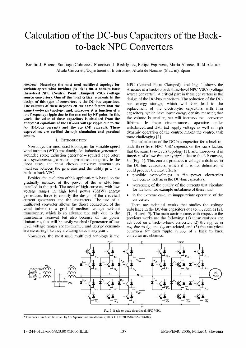
Calculation of the DC-bus Capacitors of the Back- to-back NPC Converters Emilio J. Bueno, Santiago Cobreces, Francisco J. Rodriguez, Felipe Espinosa, Marta Alonso, Rau'l Alcaraz Alcala University/Department of Electronics, Alcala de Henares (Madrid), Spain Abstract-Nowadays the most used multilevel topology for variable-speed wind turbines (WTs) is the a back-to back three-level NPC (Neutral Point Clamped) VSCs (voltage source converter). One of the most critical elements in the design of this type of converters is the DC-bus capacitors. The calculus of these depends on the same factors that the same two-levels topology, and, moreover it is function of a low frequency ripple due to the current by NP point. In this work, the value of these capacitors is obtained from the analytical equations of the DC-bus voltage ripple due to the iDC (DC-bus current) and the iNp (NP current). These expressions are verified through simulation and practical results. I. INTRODUCTION Nowadays the most used topologies for variable-speed wind turbines (WTs) are: doubly-fed induction generator - wounded rotor; induction generator - squirrel cage rotor; and synchronous generator - permanent magnets. In the three cases, the most chosen converter structure as interface between the generator and the utility grid is a back-to-back VSC. Besides, the evolution of this application is based on the gradually increase of the power of the wind-turbine installed in the park. The need of high currents, with low voltage ranges in high level power (3MW) energy generation, force to modify the design of the electrical current generators and the converters. The use of a multilevel converter allows the direct connection of the wind turbine to a grid of medium voltage without transformer, which is an advance not only due to the transformer removal but also because of the power limitations, that will be easily reached if generator of low level voltage ranges are maintained and energy demands are increasing like they are doing since many years. Nowadays, the most used multilevel topology is the NPC (Neutral Point Clamped), and Fig. 1 shows the structure of a back-to back three-level NPC VSCs (voltage source converter). A critical part in these converters is the design of the DC-bus capacitors. The reduction of the DC- bus energy storage, which will then lead to the replacement of the electrolytic capacitors with film capacitors, which have lower energy density meaning that the volume is smaller, but will increase the converter lifetime. In these circumstances, operation under unbalanced and distorted supply voltage as well as high dynamic operation of the control makes the control task more challenging [1]. The calculation of the DC-bus capacitor for a back-to- back three-level NPC VSC depends on the same factors that the same two-levels topology [1], and, moreover it is function of a low frequency ripple due to the NP current, iNp (Fig. 1). This current produces a voltage unbalance in the DC-bus capacitors, which if it is not delimited, it could produce the next effects: * possible over-voltages in the power electronics devices, as well as in the DC-bus capacitors; * worsening of the quality of the currents that circulate for the load, for example unbalance of these; and * in the extreme case, an inappropriate operation of the converter. There are technical works that studies the voltage unbalance in the DC-bus capacitors due to iNp, such as [2], [3], [4] and [5]. The main contributions with respect to the previous works are the following: (1) these analyses are achieved on a back-to-back converter, (2) the ripples in UDC due to iDC and iNp are related, and (3) the analytical equations for each ripple in UDC of a back to back converter are obtained. N Fig. 1. Back-to-back three level NPC VSC. *This work has been financed by the Spanish administration (CICYT: DPI2002-04555-C04-04). 1-4244-0121-6/06/$20.00 ©2006 IEEE 137 EPE-PEMC 2006, Portoro2, Slovenia
Transcript of Calculation of the DC-bus Capacitors of the Back-to-back NPC Converters
Calculation of the DC-bus Capacitors of the Back-to-back NPC Converters
Emilio J. Bueno, Santiago Cobreces, Francisco J. Rodriguez, Felipe Espinosa, Marta Alonso, Rau'l AlcarazAlcala University/Department of Electronics, Alcala de Henares (Madrid), Spain
Abstract-Nowadays the most used multilevel topology forvariable-speed wind turbines (WTs) is the a back-to backthree-level NPC (Neutral Point Clamped) VSCs (voltagesource converter). One of the most critical elements in thedesign of this type of converters is the DC-bus capacitors.The calculus of these depends on the same factors that thesame two-levels topology, and, moreover it is function of alow frequency ripple due to the current by NP point. In thiswork, the value of these capacitors is obtained from theanalytical equations of the DC-bus voltage ripple due to theiDC (DC-bus current) and the iNp (NP current). Theseexpressions are verified through simulation and practicalresults.
I. INTRODUCTION
Nowadays the most used topologies for variable-speedwind turbines (WTs) are: doubly-fed induction generator -wounded rotor; induction generator - squirrel cage rotor;and synchronous generator - permanent magnets. In thethree cases, the most chosen converter structure asinterface between the generator and the utility grid is aback-to-back VSC.
Besides, the evolution of this application is based on thegradually increase of the power of the wind-turbineinstalled in the park. The need of high currents, with lowvoltage ranges in high level power (3MW) energygeneration, force to modify the design of the electricalcurrent generators and the converters. The use of amultilevel converter allows the direct connection of thewind turbine to a grid of medium voltage withouttransformer, which is an advance not only due to thetransformer removal but also because of the powerlimitations, that will be easily reached if generator of lowlevel voltage ranges are maintained and energy demandsare increasing like they are doing since many years.Nowadays, the most used multilevel topology is the
NPC (Neutral Point Clamped), and Fig. 1 shows thestructure of a back-to back three-level NPC VSCs (voltagesource converter). A critical part in these converters is thedesign of the DC-bus capacitors. The reduction of the DC-bus energy storage, which will then lead to thereplacement of the electrolytic capacitors with filmcapacitors, which have lower energy density meaning thatthe volume is smaller, but will increase the converterlifetime. In these circumstances, operation underunbalanced and distorted supply voltage as well as highdynamic operation of the control makes the control taskmore challenging [1].
The calculation of the DC-bus capacitor for a back-to-back three-level NPC VSC depends on the same factorsthat the same two-levels topology [1], and, moreover it isfunction of a low frequency ripple due to the NP current,iNp (Fig. 1). This current produces a voltage unbalance inthe DC-bus capacitors, which if it is not delimited, itcould produce the next effects:* possible over-voltages in the power electronics
devices, as well as in the DC-bus capacitors;* worsening of the quality of the currents that circulate
for the load, for example unbalance of these; and* in the extreme case, an inappropriate operation of the
converter.There are technical works that studies the voltage
unbalance in the DC-bus capacitors due to iNp, such as [2],[3], [4] and [5]. The main contributions with respect to theprevious works are the following: (1) these analyses areachieved on a back-to-back converter, (2) the ripples inUDC due to iDC and iNp are related, and (3) the analyticalequations for each ripple in UDC of a back to backconverter are obtained.
N
Fig. 1. Back-to-back three level NPC VSC.
*This work has been financed by the Spanish administration (CICYT: DPI2002-04555-C04-04).
1-4244-0121-6/06/$20.00 ©2006 IEEE 137 EPE-PEMC 2006, Portoro2, Slovenia
II. RELATION BETWEEN THE CALCULUS OF THE DC-BUSCAPACITORS IN CONVERTERS OF TWO-LEVELS AND THREE-
LEVELSThe CDC calculation for two-levels VSCs connected to
the utility grid depends on the application kind. This way,if the VSC is working as:* PWM rectifier. CDC should take the value:
DCiDCTSW -
CD.2AuDC 2uDCAuDC
the values of the capacitors can cause effects verynegative in the NP voltage balance.
UDC INPR
(1)
where AUDC is the maximum allowed ripple. IfSn = 100kVA, Tsw = 400,us, UDC take the minimumvalue (610V), and AUDC is set to 10% of UDC, then,CDC . 537.5,uF . This result is very conservativebecause it implies that the DC-bus capacitor isdischarging to nominal power during half of thecommutation period. In the practice, the dischargetime, depends on the load, but, in general, it isconsiderably smaller.
* Activefilter. The worst situation takes place when it isnecessary to balance a load of negative sequence tonominal power. In these circumstances, the ripple istwice the utility grid frequency, and CDC should takethe value [1]:
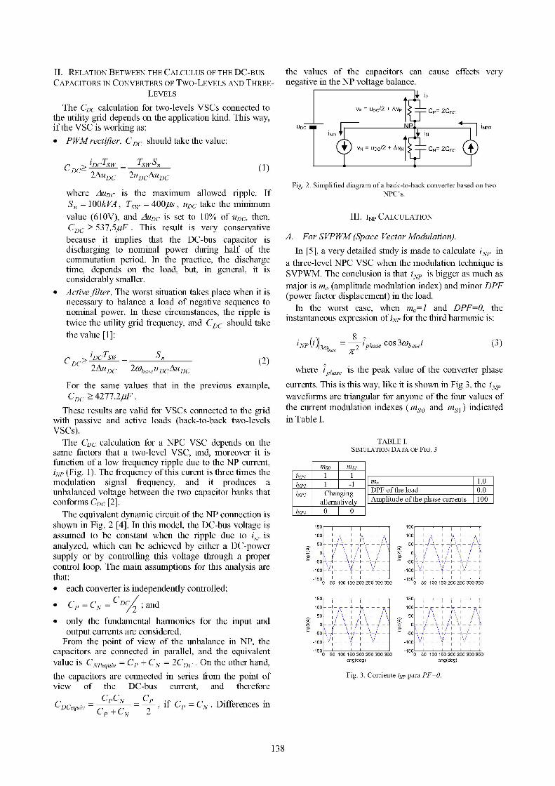
Fig. 2. Simplified diagram of a back-to-back converter based on twoNPC's.
III INP CALCULATION
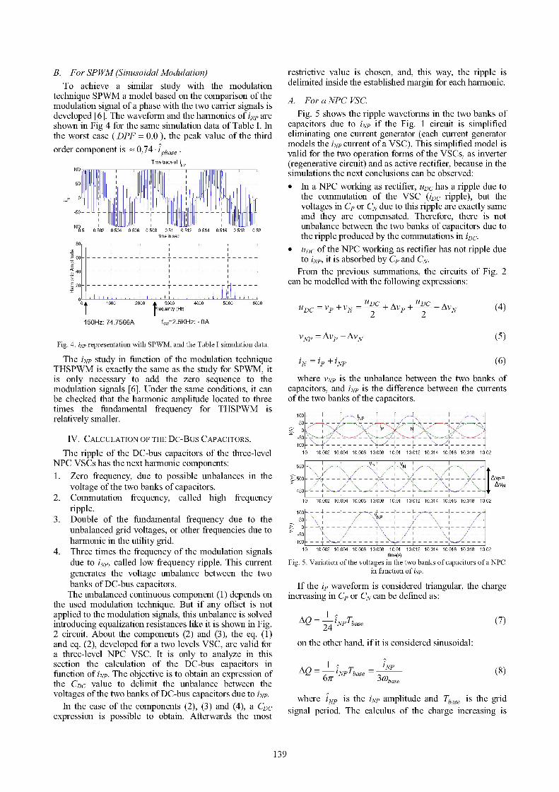
A. For SVPWM (Space Vector Modulation).In [5], a very detailed study is made to calculate iNP in
a three-level NPC VSC when the modulation technique isSVPWM. The conclusion is that iNP is bigger as much asmajor is ma (amplitude modulation index) and minor DPF(power factor displacement) in the load.
In the worst case, when ma=1 and DPF=O, theinstantaneous expression of iNp for the third harmonic is:
( 8p'NP\!)l3w,b,, - 1paecs3i,, (3)
iDCTSW SnCDC. D = D2AuDC 2cobaseUDCAuDC
(2)
For the same values that in the previous example,CDC 2 4277.2,UF.
These results are valid for VSCs connected to the gridwith passive and active loads (back-to-back two-levelsVSCs).
The CDC calculation for a NPC VSC depends on thesame factors that a two-level VSC, and, moreover it isfunction of a low frequency ripple due to the NP current,iNp (Fig. 1). The frequency of this curent is three times themodulation signal frequency, and it produces aunbalanced voltage between the two capacitor banks thatconforms CDC [2].The equivalent dynamic circuit of the NP connection is
shown in Fig. 2 [4]. In this model, the DC-bus voltage isassumed to be constant when the ripple due to iNP isanalyzed, which can be achieved by either a DC-powersupply or by controlling this voltage through a propercontrol loop. The main assumptions for this analysis arethat:* each converter is independently controlled;
* CP = CN = CDc; and* only the fundamental harmonics for the input and
output cuffents are considered.From the point of view of the unbalance in NP, the
capacitors are connected in parallel, and the equivalentvalue is CNPequiv = CP + CN = 2CDC . On the other hand,the capacitors are connected in series from the point ofview of the DC-bus current, and therefore
_ CPCN CpCDCequiv - = if CP = CN. Differences in
where lphase is the peak value of the converter phase
currents. This is this way, like it is shown in Fig 3, the iNPwaveforms are triangular for anyone of the four values ofthe current modulation indexes ( ms0 and ms1 ) indicatedin Table I.
TABLE I.SIMULATION DATA OF FIG. 3
MsoMS1
iNP2 1 11.iNP3 hngn DPF of the load 0.0i.,\aP t
ChangingAmplitude ofthe phase currents 100alternatively
iNP4 I O
150
1 00 _ _ _10
50 - -lc- I
50 - 4-
-100
150
100
50
c-* 50
-100
-150 Il -150 Il0 50 100 150 200 250 300 350 0 50 100 150 200 250 300 350
150 150
100 -1 0050 50_
C-Q 0 - 0
-50 -50
-100V_I _ _ l _a
1500 50 100 150 200 250 300 350
ang(deg)
-100 -I_ I_ _IkI_
1500 50 100 150 200 250 300 350
ang(deg)
Fig. 3. Corriente iNp para PF=O.
138
B. For SPWM (Sinusoidal Modulation)To achieve a similar study with the modulation
technique SPWM a model based on the comparison of themodulation signal of a phase with the two carrier signals isdeveloped [6]. The waveform and the harmonics of iNp areshown in Fig 4 for the same simulation data of Table I. Inthe worst case (DPF = 0.0), the peak value of the thirdorder component is 0,74. 'phase
Time trace of iNP
L100 I
0.5 0.502 0.504 0.506 0.508 0.51 0.512 0.514 0.516 0.518 0.52
80
-o 660
< 40--
20 - -----l_ ___
0 ~IO A
12 . 1
It
time in sec
1000 2000 4 3000[requency (Hz)
150Hz: 74.7566A
restrictive value is chosen, and, this way, the ripple isdelimited inside the established margin for each harmonic.
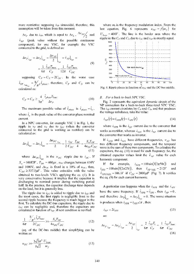
A. For a NPC VSC.Fig. 5 shows the ripple waveforms in the two banks of
capacitors due to iNp if the Fig. 1 circuit is simplifiedeliminating one current generator (each current generatormodels the iNp current of a VSC). This simplified model isvalid for the two operation forms of the VSCs, as inverter(regenerative circuit) and as active rectifier, because in thesimulations the next conclusions can be observed:
In a NPC working as rectifier, uDc has a ripple due tothe commutation of the VSC (iDC ripple), but thevoltages in Cp or CN due to this ripple are exactly sameand they are compensated. Therefore, there is notunbalance between the two banks of capacitors due tothe ripple produced by the commutations in iDC.
* uDC of the NPC working as rectifier has not ripple dueto iNp, it is absorbed by Cp and CN.From the previous summations, the circuits of Fig. 2
can be modelled with the following expressions:.1L I1A1U 11I4000 5000 6000 UDC UDCUDC = VP +VN = +Avp + +AvN
2 2fsw=2.5KHz: -OA
(4)
Fig. 4. iNp representation with SPWM, and the Table I simulation data.
The iNp study in function of the modulation techniqueTHSPWM is exactly the same as the study for SPWM, itis only necessary to add the zero sequence to themodulation signals [6]. Under the same conditions, it canbe checked that the harmonic amplitude located to threetimes the fundamental frequency for THSPWM isrelatively smaller.
IV. CALCULATION OF THE Dc-Bus CAPACITORS.The ripple of the DC-bus capacitors of the three-level
NPC VSCs has the next harmonic components:1. Zero frequency, due to possible unbalances in the
voltage of the two banks of capacitors.2. Commutation frequency, called high frequency
ripple.3. Double of the fundamental frequency due to the
unbalanced grid voltages, or other frequencies due toharmonic in the utility grid.
4. Three times the frequency of the modulation signalsdue to iNp, called low frequency ripple. This currentgenerates the voltage unbalance between the twobanks of DC-bus capacitors.The unbalanced continuous component (1) depends on
the used modulation technique. But if any offset is notapplied to the modulation signals, this unbalance is solvedintroducing equalization resistances like it is shown in Fig.2 circuit. About the components (2) and (3), the eq. (1)and eq. (2), developed for a two levels VSC, are valid fora three-level NPC VSC. It is only to analyze in thissection the calculation of the DC-bus capacitors infunction of iNp. The objective is to obtain an expression ofthe CDC value to delimit the unbalance between thevoltages of the two banks of DC-bus capacitors due to iNp.
In the case of the components (2), (3) and (4), a CDCexpression is possible to obtain. Afterwards the most
VNP = Avp - AvN (5)
(6)IN = Ip + INPwhere VNp is the unbalance between the two banks of
capacitors, and iNp is the difference between the currentsof the two banks of the capacitors.
100 _50
-50-100 _
i
IpIC
10 10.002 10.004 10.006 10.008 10.01 10.012 10.014 10.016 10.018 10.02
550 _N - --17 pT --r vN_^ r A> 500
450VN
10 10.002 10.004 10.006 10.008 10.01 10.012 10.014 10.016 10.018 10.02
I:Ir10050 INP
> 0 - -\-----t--7r--
-1- ---50-100- -- -- -- - -
10 10.002 10.004 10.006 10.008 10.01 10.012 10.014 10.016 10.018 10.02time(s)
Fig. 5. Variation of the voltages in the two banks of capacitors of a NPCin function of iNp.
If the ip waveform is considered triangular, the chargeincreasing in Cp or CN can be defined as:
I1 ^AQ = 1lNPTbase24
on the other hand, if it is considered sinusoidal:
A=-NPTbase =6ff 30)base
(7)
(8)
where iNP is the iNp amplitude and Tbase is the gridsignal period. The calculus of the charge increasing is
139
more restrictive supposing iNp sinusoidal, therefore, thisassumption will be taken from this moment.
Avp due to iNp, which is equal to AvN AvNP and
VNP (peak value without the possible continuouscomponent), for one VSC, for example the VSCconnected to the grid, is defined as:
/\V A|i=VNA A2=P 2 ~NPZ
l INPTbase =
6ff Cp1 lNPTbase
12ff CDC
supposing Cp = CN = 2CDC. In the worst case
iNP 3 = Z2 lphase rtherefore, Cp and CN can be'NP 8asccalculated as:
CP -C > 4 lphaseTbaseI3T3 Avp (10)
The maximum possible value of iphase is iphase = in ,
where in is the peak value of the converter phase nominalcurrent.
In a NPC converter, for example VSC 1 in Fig. 1, theripple in vp and VN due to iDC (when the converterconnected to the grid is working as rectifier) can becalculated as:
Avel. A^VN|. =DC 'DC
AuDC 1 I'DC TSW _ SnTSW2 2 CDC 4 4UDCCDC
(1 1)
where AUDC |IDC is the UDC ripple due to iDC If
Sn = 1OOKW, TSW = 400,us, UDC changes between 61OVand 1 OOOV, and AUDc is fixed in a 10% of UDC, then,CDC 2537.5,uF. This value coincides with the valueobtained to two-levels VSCs applying the ec. (1). It isvery conservative because it implies that the capacitor isdischarging to nominal power during switching periodhalf. In the practice, the capacitor discharge time dependson the load, but it is generally less.
The ripple due to iDC is added to ripple due to iNp, andthe most cases, the first ripple is negligible front to thesecond ripple because the frequency is much bigger in thefirst. To calculate the DC-bus capacitors, the ripple due toiDC can be negligible and, therefore the capacitors arecalculated in function of iNp, ifnext condition is verified:
16ff
2 inTbase
2CDC>>SnTSW4U1DCCDC
where mf is the frequency modulation index. From thelast equation, Fig. 6 represents UDC = f(mf ) for
Ubase =400V . The line is the border area where theripple in the Cp and CN due to iDC and iNp is exactly equal.
1000
900 _
800
700
600
o 500(9) =350400_
300_Mailn ripple due to iNP
200 - - A- - A- - - --1-- I- -
Maih ripple due to l II I I
100 r
0 10 20 30 40 50 60 70 80 90 100mf
Fig. 6. Ripple places in function of uDC and the DC-bus middle.
B. For a back-to-back NPC VSC.Fig. 2 represents the equivalent dynamic circuit of the
NP connection for a back-to-back three-level NPC VSC.The iNp current circulates by Cp and CN, and that producesthe voltage unbalance, take the value:
iNP (t ) = 'NPR (t ) - 'NPI (t ) (14)
where iNPR is the iNP current due to the converter thatworks as rectifier, whereas iNPI is the iNP current due tothe converter that works as inverter.
If iNPR and iNPI have different frequencies, VNP hastwo different frequency components, and the temporalwave is the sum ofthese two components. To calculate thecapacitors, the eq. (10) is used for each frequency. So, theobtained capacitor values limit the VNP value for eachharmonic component.
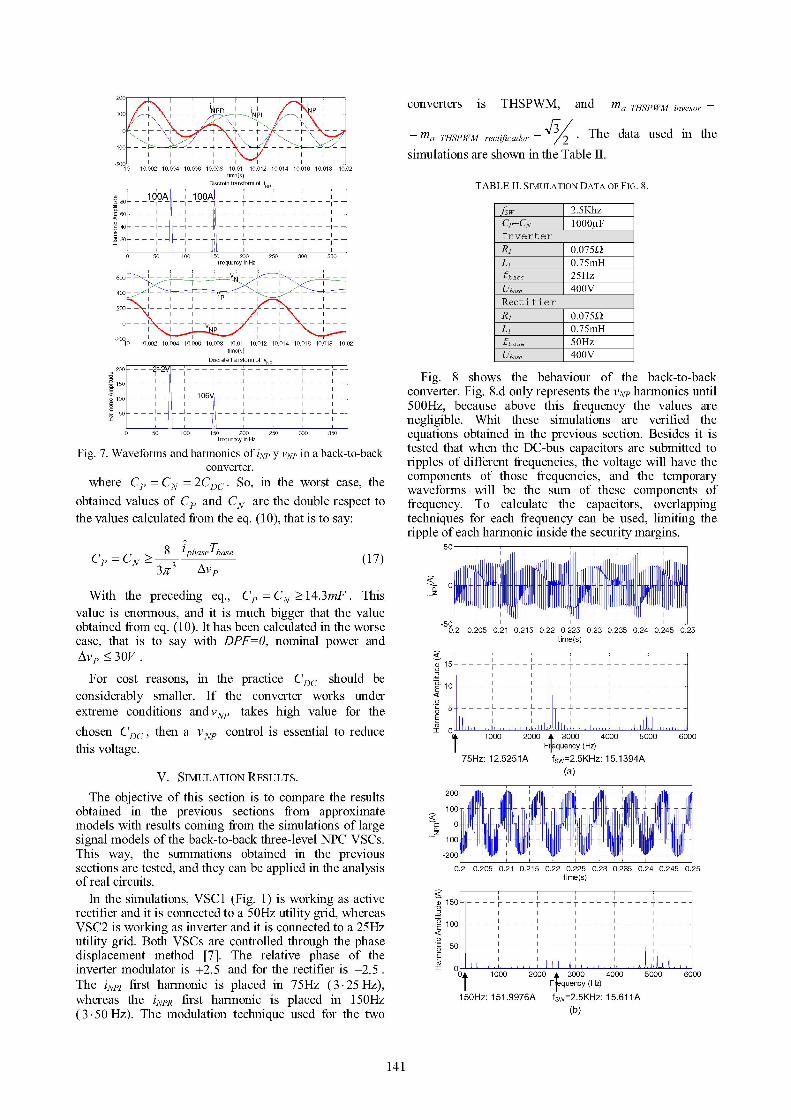
If for example, iNpR = 100 sin(3(2;T50t)) and
iNPI = 100 sin(3(2;T25t)), then VNP75Hz = 212V andVNp15oHz = 106.1V if CDC = 2000uF (Fig. 7). It verifiesthe eq. (9) for each current harmonic.
A particular case happens when the iNpR and the iNPIhave the same frequency. If iNPR = iNPII then 1Np = ,and therefore AvplDC = AvNIDC = 0. The worse situation
is produces when iNpR = iNpI/J , then:
(15)INP 2'NPI
so:
(12)
(eq. of the DC-bus middle) that simplifying can bewritten as:
Avep.Np AVNN AvNP1N1NP
=
2
-2 iNP I 1 NPTbase
6;T CP 6;T CDC(16)
3 F3ff UbaseU1DC» 81 r (13)
140
100 NPR P
-100
-200.10 10.002 10.004 10.006 10.008 10.01 10.012 10.014 10.016 10.018 10.02
time(s)Discrete transform of iD
converters is THSPWM, and ma THSPWM invesor =
=Ma THSPWM rectificador = .3/ The data used in thesimulations are shown in the Table II.
TABLE II. SIMULATION DATA OF FIG. 8.
0 50 100 150 200 250 300 350frequency in Hz
600
400
200/
-20010 10.002 10.004 10.006 10.008 10.01 10.012 10.014 10.016 10.018 10.02
time(s)Discrete transform of VN
200 -4
*Q150 _F I___I___I___I
100-
E 0
050 100 150 200 250 300 350frequency in Hz
Fig. 7. Waveforms and harmonics of iNp y VNp in a back-to-backconverter.
where CP = CN = 2CDC. So, in the worst case, theobtained values of CP and CN are the double respect tothe values calculated from the eq. (10), that is to say:
CP = C > 8 iphaseTbase (17)
With the preceding eq., CP = CN . 14.3mF. Thisvalue is enormous, and it is much bigger that the valueobtained from eq. (10). It has been calculated in the worsecase, that is to say with DPF=0, nominal power andAvp < 30V.For cost reasons, in the practice CDC should be
considerably smaller. If the converter works underextreme conditions and VNP takes high value for thechosen CDC, then a VNP control is essential to reducethis voltage.
V. SIMULATION RESULTS.The objective of this section is to compare the results
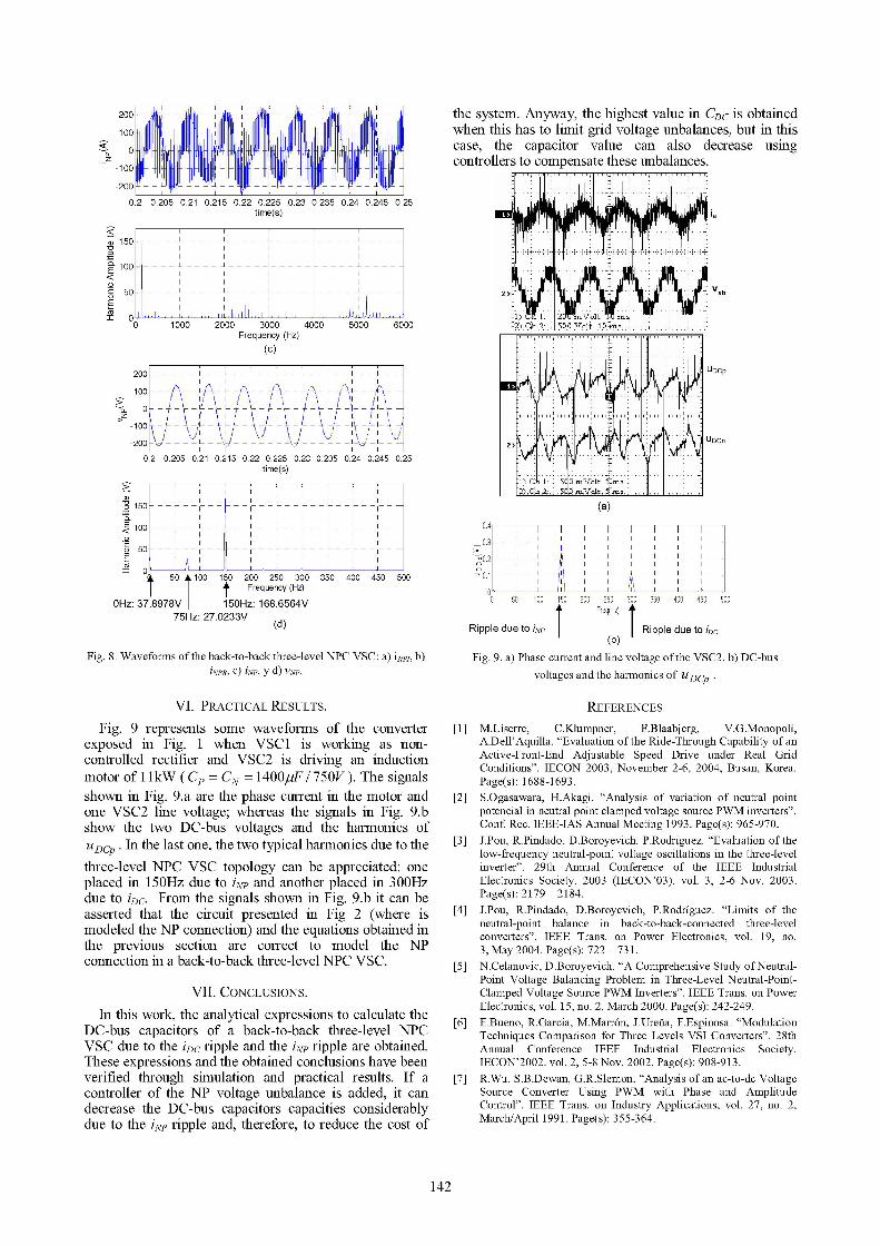
obtained in the previous sections from approximatemodels with results coming from the simulations of largesignal models of the back-to-back three-level NPC VSCs.This way, the summations obtained in the previoussections are tested, and they can be applied in the analysisof real circuits.
In the simulations, VSC1 (Fig. 1) is working as activerectifier and it is connected to a 50Hz utility grid, whereasVSC2 is working as inverter and it is connected to a 25Hzutility grid. Both VSCs are controlled through the phasedisplacement method [7]. The relative phase of theinverter modulator is +2.5 and for the rectifier is -2.5 .The iNpI first harmonic is placed in 75Hz (3.25 Hz),whereas the iNpR first harmonic is placed in 150Hz(3 50 Hz). The modulation technique used for the two
Fig. 8 shows the behaviour of the back-to-backconverter. Fig. 8.d only represents the VNp harmonics until500Hz, because above this frequency the values arenegligible. Whit these simulations are verified theequations obtained in the previous section. Besides it istested that when the DC-bus capacitors are submitted toripples of different frequencies, the voltage will have thecomponents of those frequencies, and the temporarywaveforms will be the sum of these components offrequency. To calculate the capacitors, overlappingtechniques for each frequency can be used, limiting theripple of each harmonic inside the security margins.
50
I " III lr'0I8I''1 11 lal' -"1II1
-50 I0.2 0.205 0.21 0.215 0.22 0.225 0.23 0.235 0.24 0.245 0.25
time(s)
-o
J 0 IIli I II W........ .11 lL1 A IIIIIIL,1000 2000 X u30 04000 5000 bUUU 00
| 4r quency(z75Hz: 12.5251A fsw=2-5KHz: 1 5.1394A
(a)
200 - - - - - -
100
z-100
I).2 0.205 0.21 0.215 0.22 0.225 0.23 0.235 0.24 0.245 0.2
time(s)
0D 150 - .
100E
50-_
i1000 2000 3000 4000 5000 6000F equency (Hz)
150Hz: 151 .9976A fsw=2.5KHz: 15.611 A
(b)
141
2001'II,
--
_Z
,~
UDI%
.25
the system. Anyway, the highest value in CDC is obtainedwhen this has to limit grid voltage unbalances, but in thiscase, the capacitor value can also decrease usingcontrollers to compensate these unbalances.
-200
0.2 0.205 0.21 0.215 0.22 0.225 0.23 0.235 0.24 0.245 0.25time(s)
< 15a) 150 -
E100____E
50 -l _--
IC0 1 00(
200 _ _ _
100
a- 0
-100
9200
0 2000 3000 4000Frequency (Hz)
(c)
5000 6000
).2 0.205 0.21 0.215 0.22 0.225 0.23 0.235 0.24 0.245 0.25time(s)
50 A 10 R5 20 25 30 35 40 45 0450III~~~~~50
(a)0.4_
0.3 _
-0.2
' 0.1
O \,0T T t Frequency (Hz)
OHz: 37.8978V 150Hz: 168.6564V75Hz: 27.0233V
(d)
Fig. 8. Waveforms of the back-to-back three-level NPC VSC: a) iNpI, b)iNPR, C) iNP, y d) VNP.
VI. PRACTICAL RESULTS.
Fig. 9 represents some waveforms of the converterexposed in Fig. 1 when VSC1 is working as non-controlled rectifier and VSC2 is driving an inductionmotor of 11kW ( CP = CN = 1400,F / 750V ). The signalsshown in Fig. 9.a are the phase current in the motor andone VSC2 line voltage; whereas the signals in Fig. 9.bshow the two DC-bus voltages and the harmonics ofUDCP . In the last one, the two typical harmonics due to thethree-level NPC VSC topology can be appreciated: oneplaced in 150Hz due to iNp and another placed in 300Hzdue to iDC. From the signals shown in Fig. 9.b it can beasserted that the circuit presented in Fig 2 (where ismodeled the NP connection) and the equations obtained inthe previous section are correct to model the NPconnection in a back-to-back three-level NPC VSC.
VII. CONCLUSIONS.In this work, the analytical expressions to calculate the
DC-bus capacitors of a back-to-back three-level NPCVSC due to the iDC ripple and the iNp ripple are obtained.These expressions and the obtained conclusions have beenverified through simulation and practical results. If acontroller of the NP voltage unbalance is added, it candecrease the DC-bus capacitors capacities considerablydue to the iNp ripple and, therefore, to reduce the cost of
Ripple dL
Il50 100 150
ue to iNP
_1___I- __-I _____ , ---I
_I_ _l__ __I_ _l_All 1K
200 250 300 350 400 450 500Freq(Hz)'
Ripple due to iDC1/1%* (b)
Fig. 9. a) Phase current and line voltage of the VSC2. b) DC-busvoltages and the harmonics of UDCP
REFERENCES
[1] M.Liserre, C.Klumpner, F.Blaabjerg, V.G.Monopoli,A.Dell'Aquilla. "Evaluation of the Ride-Through Capability of anActive-Front-End Adjustable Speed Drive under Real GridConditions". IECON 2003, November 2-6, 2004, Busan, Korea.Page(s): 1688-1693.
[2] S.Ogasawara, H.Akagi. "Analysis of variation of neutral pointpotencial in neutral point clamped voltage source PWM inverters".Conf. Rec. IEEE-IAS Annual Meeting 1993. Page(s): 965-970.
[3] J.Pou, R.Pindado, D.Boroyevich, P.Rodriguez. "Evaluation of thelow-frequency neutral-point voltage oscillations in the three-levelinverter". 29th Annual Conference of the IEEE IndustrialElectronics Society, 2003 (IECON'03), vol. 3, 2-6 Nov. 2003.Page(s): 2179 - 2184.
[4] J.Pou, R.Pindado, D.Boroyevich, P.Rodriguez. "Limits of theneutral-point balance in back-to-back-connected three-levelconverters". IEEE Trans. on Power Electronics, vol. 19, no.3, May 2004. Page(s): 722 - 731.
[5] N.Celanovic, D.Boroyevich. "A Comprehensive Study of Neutral-Point Voltage Balancing Problem in Three-Level Neutral-Point-Clamped Voltage Source PWM Inverters". IEEE Trans. on PowerElectronics, vol. 15, no. 2, March 2000. Page(s): 242-249.
[6] E.Bueno, R.Garcia, M.Marr6n, J.Urefia, F.Espinosa. "ModulationTechniques Comparison for Three Levels VSI Converters". 28thAnnual Conference IEEE Industrial Electronics Society.IECON'2002. vol. 2, 5-8 Nov. 2002. Page(s): 908-913.
[7] R.Wu, S.B.Dewan, G.R.Slemon. "Analysis of an ac-to-dc VoltageSource Converter Using PWM with Phase and AmplitudeControl". IEEE Trans. on Industry Applications, vol. 27, no. 2,March/April 1991. Page(s): 355-364.
142
Vab
UDCp
UDCn
0.
a)-g 150
.9E 100
0 50EJ 0
1: 1: r r r 1: 1:
;2
TV
-I I-
-I 1-