
Datapath scheduling with multiple supply voltages and level converters
Three-Level/-Phase PWM Converters Dc-LinkVoltages Ripple Reduction Technique
in the αβ Reference FrameJoabel Moia, Arnaldo J. Perin, and Marcelo L. Heldwein
Federal University of Santa Catarina — UFSCElectrical Engineering Department / Power Electronics Institute — INEP
PO box: 5119 — 88040-970 — Florianopolis, SC, BRAZILPhone: +55(48)3721–9204 / Fax: +55(48)3234–5422
E-mail: joabel ; arnaldo.perin ; heldwein @inep.ufsc.br
Abstract—This work is part of a research effort to evaluateand develop power converter systems that are to be used infuture bipolar dc active distribution networks. A characteristicof such networks is that the power levels across each of the dc-buses can be highly unbalanced at steady-state. Therefore, thefront-end bidirectional rectifier system is required to provide wellregulated, balanced and low ripple dc voltages to the bipolar dcbus. A straightforward modulation technique is introduced herefor three-level/-phase bidirectional PWM rectifiers. The methodis based in the analysis of three-level converters in the αβ0stationary reference frame, where the ac currents and duty-cycle α and β components are used to compute the required0-axis duty-cycle that guarantees that the dc-link center pointlow frequency current components are nullified. The techniqueis implemented in a carrier-based PWM modulation scheme.Implementation in a digital processor is used in a three-levelbidirectional converter lab prototype. The prototype is testedto present experimental results of the proposed technique. Themain consequences of the proposed technique are that bothbipolar dc bus voltages present negligible voltage ripple evenunder highly unbalanced bus power levels and variable ac-sidepower factor, which is appropriate to interface a dc bipolardistribution network to an ac system with controlable reactivepower injection. An important secondary effect is that the rmscurrent value is greatly reduced in the converter dc bus capacitor.
Keywords – three-level converter; neutral point current;dc-link voltage ripple; stationary frame analysis.
I. INTRODUCTION
Three-level/-phase PWM (3L-PWM) converters find appli-cations in medium voltage (MV) high-power applications aswell as in renewable energy and regenerative low voltage(LV) ones [1], [2]. Examples of such converters are the three-level Neutral Point Clamped (NPC) converter [3], [4] andits modified versions that use switches blocking the full dc-link voltage, called the modified NPC converter (NPCm) [5]here and having other nomenclatures in the literature [6–10].The NPCm topology is advantageous for LV high switchingfrequency applications due to its lower current efforts [5], [10].On the other hand, MV low switching frequency applicationsrequire lower voltage switches, where the NPC converter ex-
cels and finds numerous applications [2]. The dc-link voltagesbalance has been widely discussed in the literature [11–16].However, few works consider steady state dc-link unbalancedloads and/or power generation as can be the case for three-level rectifiers used in bipolar dc distribution networks [17].In this context, the front-end bidirectional rectifier system isrequired to provide well regulated, balanced and low ripple dcvoltages to the bipolar dc bus. A straightforward modulationtechnique is proposed here for three-level/-phase bidirectionalPWM rectifiers.
Dc-link voltage ripple reduction at the dc-link partial volt-ages for three-level PWM converters have already been pre-sented in the literature [18–25]. However, few of the workspresent all of the following characteristics: ease of implemen-tation, operation under severe steady state unbalance, openloop with complete elimination of the low frequency ripple,proper operation under wide ac-side power factor variation,low ac-side switched voltages distortion, good performanceeven with low switching frequency. The listed characteristicsare the aim of this work and are evaluated in the simulationresults section.
The proposed technique is based in the analysis of three-level converters in the αβ0 stationary reference frame, wherethe ac currents and duty-cycle α and β components are usedto compute the required 0-axis duty-cycle, which guaranteesthat the dc-link center point low frequency current componentsare nullified. The technique is implemented in a carrier-basedPWM modulation scheme. Thus, implementation in a digitalprocessor is straightforward. The main consequences of theproposed technique are that both bipolar dc bus voltagespresent negligible voltage ripple even under highly unbalancedbus power levels and varying ac-side power factor. An impor-tant secondary effect is that the rms current value is greatlyreduced in the dc bus capacitor.
This work is organized as follows. Section II presentsthe analysis of the dc-link center point current in a three-level three-phase bidirectional converter in the αβ0 stationaryreference frame and derives the conditions for the cancellationof this current based on measured current and control signals.
Simulation results of a three-level converter are presented insection III to show that the proposed center point cancelationtechnique is effective even under relatively low switchingfrequency, high dc-link power unbalance and load transientconditions. Experimental results obtained in a modern three-level bidirectional converter are presented in section IV andprove the feasibility of the current cancellation technique byshowing the reduction of the third harmonic (180 Hz) partialdc-link voltage ripple component by approximately twentytimes when compared to a standard sine PWM modulation(SPWM). Furthermore, it is shown that the current ripple at theac-side inductors is not considerably different when comparedto the SPWM, where the ripple component at the switchingfrequency is reduced with the proposed technique.
II. NEUTRAL POINT CURRENT LOCAL AVERAGE VALUECANCELLATION IN THE αβ0 REFERENCE FRAME
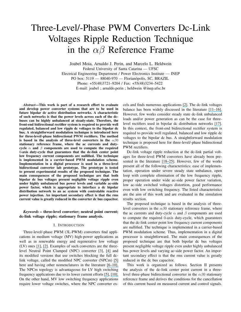
Fig. 1 shows a circuit model for 3L-PWM convertersemploying single pole triple throw switches. The circuit modelshows the output capacitors Cs and two non-equal loads Zlpand Zln across the two partial dc-link buses. An ac grid ismodeled through the ac voltage sources vj , with j = a, b, c.Switches Sj are driven by switching signals sjk, where
sjk =
+1 ; if Sj is connected to the k terminal0 ; otherwise , (1)
with k = p, 0, n are the dc-link terminals according to Fig. 1.Applying Kirchhoff’s second law to Fig. 1 leads to
Ld
dt~iabc = ~vabc − ~vs,abc + ~vN0, (2)
where ~iabc = [ia ib ic]T ; ~vabc = [va vb vc]
T ; and, ~vN0 =[vN0 vN0 vN0]T . vN0 is the instantaneous voltage from themains neutral point N to the dc-link center point 0. Consid-ering balanced dc voltages, i.e.,
vp0 = v0n =Vdc2, (3)
the pole voltages are given by
vs,j = (sjp − sjn)Vdc2 . (4)
SL
NL
L
a
isap
ia
ib
ic
isan
isa0
Sb
Sc Cs
Cs
isb0
isc0
is0
isp
isn
ig0
igp
vp0vs,a
vs,b
vs,c
va
vb
vc
vdc
v0n
ign
isbp
isbn
iscp
iscn
Av
Bv
Cv
icsp
icsn
Fig. 1. Three-phase NPC converter equivalent circuit.
The per phase switching functions are defined as
sj = sjp − sjn. (5)
Thus,
~vs,abc = [vs,a vs,b vs,c]T = Vdc
2 ~sabc = Vdc2 · [sa sb sc]
T . (6)
The resulting dc-link currents (isp, isn, is0) are
ispisnis0
=
sap sbp scpsan sbn scnsa0 sb0 sc0
·~iabc, (7)
where the switching functions sj0 are defined as
sj0 = 1− |sj | . (8)
It follows that ~13×1·~iabc = 0 in a three-wire system. Therefore,the neutral point current is0 is
is0 = − |~sabc| · (~iabc)T . (9)
Applying the local average operator at the voltages at theac terminals 〈~vs,abc〉 gives
〈~vs,abc〉=1
Ts
∫ Ts
t−Ts~vs,abc dt =
Vdc2~dabc, (10)
where ~dabc = [da db dc]T are the per phase equivalent duty-
cycles in a switching period Ts.
Assuming a balanced sinusoidal three-phase ac system with
vj = V sin(ωt+ θj) (11)
with θa = 0; θb = −2π/3; and, θc = +2π/3. The modulationindex M is defined as
M =2V
Vdc. (12)
The ac currents are ij = I sin(ωt + θj + φ), where φ is thecurrent displacement angle to the ac voltages. Matrix T isClarke’s transform from abc coordinates to the αβ0 stationaryreference frame. This transform is defined as
T =
√2
3
1 −1/2 −1/2
0√
3/
2 −√
3/
2
1/√
2 1/√
2 1/√
2
, (13)
Applying the local average operator and the αβ0 frametransformation to (9) leads to the local average value of thecenter point current 〈is0〉
〈is0〉 = − |T−1 ~dαβ0 |(T−1~iαβ0
)T, (14)
with ~dαβ0 = [dα dβ d0]T and ~iαβ0 = [iα iβ i0]T . Solving
(14) for a three-wire system (i.e. i0 = 0) results
〈is0〉 = − |√
63 dα +
√3
3 d0︸ ︷︷ ︸=f1
|(√
63 iα
)−
|−√
66 dα +
√2
2 dβ +√
33 d0︸ ︷︷ ︸
=f2
|(−√
66 iα +
√2
2 iβ
)−
|−√
66 dα −
√2
2 dβ +√
33 d0︸ ︷︷ ︸
=f3
|(−√
66 iα −
√2
2 iβ
) , (15)
which is a general expression defining the current 〈is0〉 in theαβ0 reference. Equation (15) shows that the zero axis duty-cycle influences 〈is0〉. Functions f1, f2 and f3 are used in thefollowing to define the 0-axis duty-cycle that cancels the lowfrequency voltage ripple at the dc buses.
The objective here is to guarantee that 〈is0〉 equals thedc-current value Ig0 of the center point of the dc busesloads ig0 (cf. Fig. 1). This condition makes that the dc-buses partial voltage only present ripple generated by theswitching frequency harmonics. Thus, high quality voltageswill be observed. The solution to this challenge is given bysolving (15) for d0 with 〈is0〉 = Ig0. This results in a 0-axisduty-cycle dcanc
0 that cancels the voltage ripple,
dcanc0 =
dcanc0,1 if f1 ≥ 0, f2 ≥ 0, f3 < 0dcanc
0,2 if f1 ≥ 0, f2 < 0, f3 ≥ 0dcanc
0,3 if f1 ≥ 0, f2 < 0, f3 < 0dcanc
0,4 if f1 < 0, f2 ≥ 0, f3 ≥ 0dcanc
0,5 if f1 < 0, f2 ≥ 0, f3 < 0dcanc
0,6 if f1 < 0, f2 < 0, f3 ≥ 0
, (16)
where
dcanc0,1 =
(−√
2iαiα+√
3iβ+√
62
iβiα+√
3iβ
)dα+(√
62
dβiαiα+√
3iβ
)−(
3√
22
Ig0iα+√
3iβ
) (17)
dcanc0,2 =
( √2iα
−iα+√
3iβ+√
62
iβ−iα+
√3iβ
)dα+(√
62
dβiα−iα+
√3iβ
)+(
3√
22
Ig0−iα+
√3iβ
) (18)
dcanc0,3 = −
√2
4dα +
3√
2
4
dβiβiα−
(3√
2
4
Ig0iα
)(19)
dcanc0,4 = −
√2
4dα +
3√
2
4
dβiβiα
+
(3√
2
4
Ig0iα
)(20)
dcanc0,5 =
( √2iα
−iα+√
3iβ+√
62
iβ−iα+
√3iβ
)dα+(√
62
dβiα−iα+
√3iβ
)−(
3√
22
Ig0−iα+
√3iβ
) (21)
dcanc0,6 =
(−√
2iαiα+√
3iβ+√
62
iβiα+√
3iβ
)dα+(√
62
dβiαiα+√
3iβ
)+(
3√
22
Ig0iα+√
3iβ
) . (22)
Variables ig0, iα and iβ are computed from the currentmeasurements, while duty-cycles dα and dβ are readily avail-able at the output of the converter controllers. A controlblock diagram that uses the proposed cancellation technique
abc
iαiβ
iβ*
iβ
iα*
Ciα
Ciβ
abc
da
Modulation
Scalar
3L-PWM
Converter
iα
Cvp,n
0n
p0
d0,avg
db
dc
sa
sb
sc
dα
dβ
d0
αβ0
*
Cvdc
dc
dc
αβ0
i
i
v
v
v
d0
canc
dα dβ
v
iαiβI_
a
c
g0
Eq. (10)
ibabc
vα
vβ
αβ0v
v
a
c
vb
vα
v β
εiα
εiβ
εvdc
εvp,n
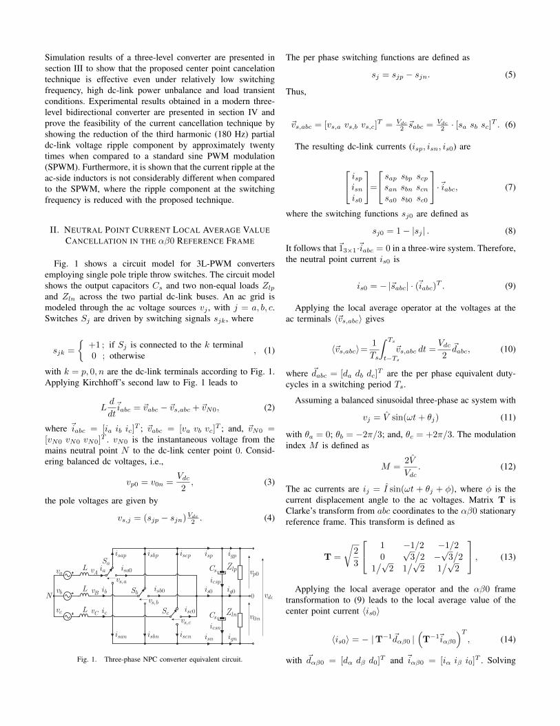
Fig. 2. Control block diagram implemented in the αβ0 reference frameincluding the proposed modulation technique according to (16), ac currentscontrol for unity power factor, dc buses partial and total voltage control.
is exemplarily presented in Fig. 2. The total dc-link voltageerror (εvdc = v∗dc − vdc) is compensated by Cvdc. The outputsignal is multiplied by the αβ measured grid-side voltagesand generate the reference currents i∗α and i∗β . The respectivecurrent errors are compensated by Ciα and Ciβ and generatethe modulation signals dα and dβ . The dc-link voltage balancecontrol loop is implemented by determining the voltage unbal-ance (εvp,n = vp0−v0n) and compensating it with Cvp,n. Thisgenerates the average value of the 0-axis control signals d0,avg .The dc-link ripple voltage cancelation loop is implemented byEq. (16), which generates the feedforward 0-axis voltage ripplecancelation signal dcanc
0 . The two 0-axis signals are summedto finally generate d0. The modulation signals dα, dβ and d0
are back-transformed to the abc reference frame and used ina scalar PWM modulator to drive the three-level rectifier.
III. SIMULATION RESULTS
The results presented in this section use a three-level con-verter that uses the control block diagram shown in Fig. 2.Considering that powers
Ph = IgpVp0 (23)
and
Pl = IgnV0n (24)
are, respectively, the upper and lower dc bus powers, the totaloutput power is
Po = Ph + Pl (25)
and the unbalance power is given by
Pu = Ph − Pl. (26)
It follows an unbalance ratio αp defined with
αp =PuPo. (27)
The simulation parameters are:• Switching frequency fs = 4 kHz;• Output total power Po = 160 kW;
• Dc-link capacitors (each): Cs = 4700µF;• Total dc-link voltage: Vdc = 800 V;• Power factor PF ∼= 1;• Modulation index: M = 0.8;• Reactive impedance (at 50 Hz): XL = ωL = 0.0314 Ω.In addition, αp = +0.35 when unbalanced powers are
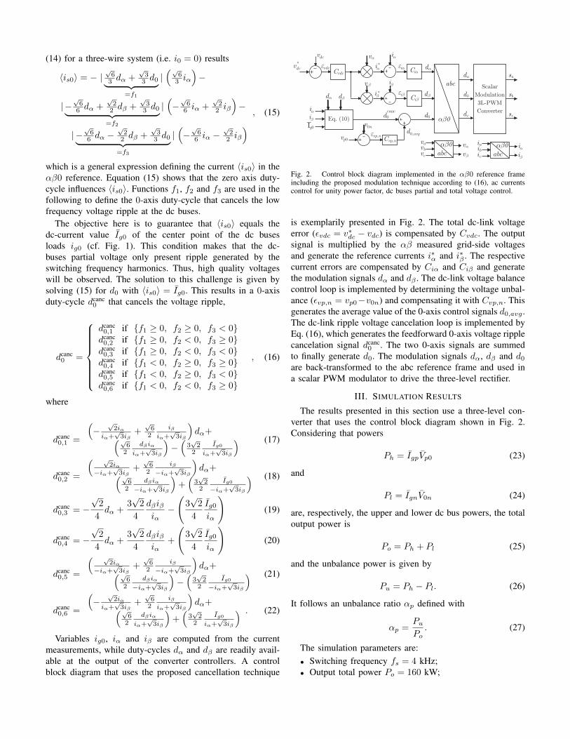
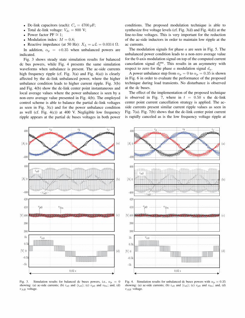
indicated.Fig. 3 shows steady state simulation results for balanced
dc bus powers, while Fig. 4 presents the same simulationwaveforms when unbalance is present. The ac-side currentshigh frequency ripple (cf. Fig. 3(a) and Fig. 4(a)) is clearlyaffected by the dc-link unbalanced power, where the higherunbalance condition leads to higher current ripple. Fig. 3(b)and Fig. 4(b) show the dc-link center point instantaneous andlocal average values where the power unbalance is seen by anon-zero average value presented in Fig. 4(b). The employedcontrol scheme is able to balance the partial dc-link voltagesas seen in Fig. 3(c) and for the power unbalance conditionas well (cf. Fig. 4(c)) at 400 V. Negligible low frequencyripple appears at the partial dc buses voltages in both power
400
0
-400
[A] (a)
400
0
-400
[A]
380
420
410
400
390
[V]
(b)
(c)
(d)
0,02 s
-1k
0
-0.5k
[V]
1k
0.5k
ia ib ic
is0
<i >s0
vp0 v0n
vAB
Fig. 3. Simulation results for balanced dc buses powers, i.e., αp = 0showing: (a) ac-side currents; (b) is0 and 〈is0〉; (c) vp0 and v0n; and, (d)vAB voltage.
conditions. The proposed modulation technique is able tosynthesize five voltage levels (cf. Fig. 3(d) and Fig. 4(d)) at theline-to-line voltages. This is very important for the reductionof the ac-side inductors in order to maintain low ripple at theac currents.
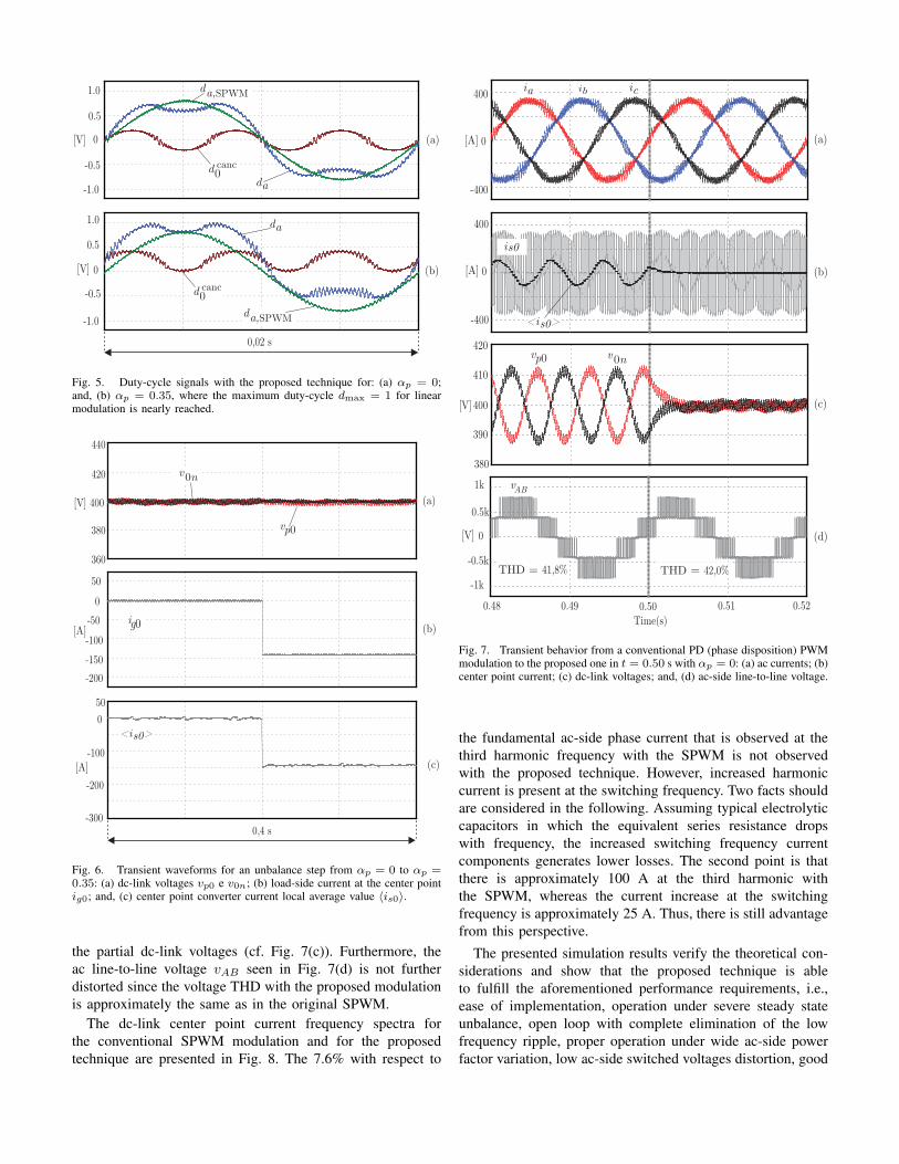
The modulation signals for phase a are seen in Fig. 5. Theunbalanced power condition leads to a non-zero average valuefor the 0-axis modulation signal on top of the computed currentcancelation signal dcanc
0 . This results in an asymmetry withrespect to zero for the phase a modulation signal da.
A power unbalance step from αp = 0 to αp = 0.35 is shownin Fig. 6 in order to evaluate the performance of the proposedtechnique during load transients. No disturbance is observedat the dc buses.
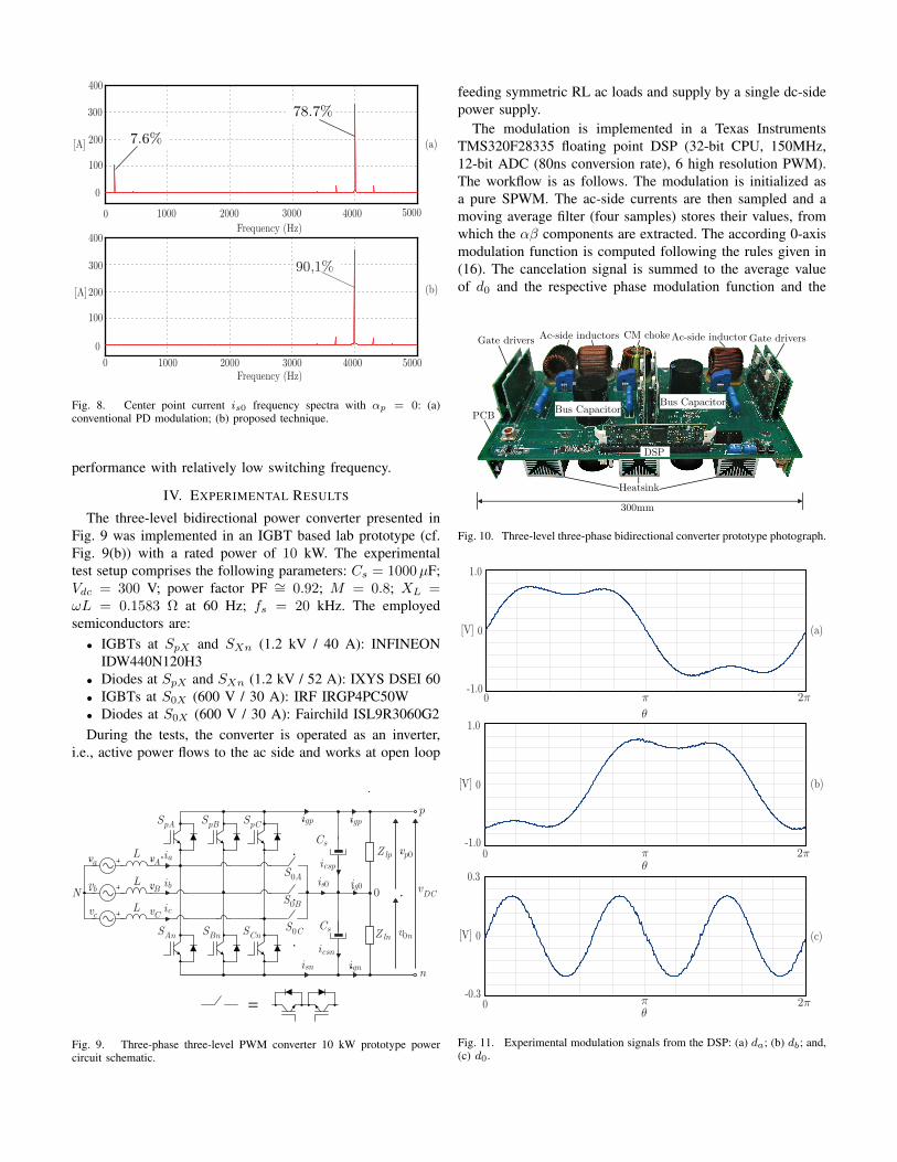
The effect of the implementation of the proposed techniqueis observed in Fig. 7, where in t = 0.50 s the dc-linkcenter point current cancellation strategy is applied. The ac-side currents present similar current ripple values as seen inFig. 7(a). Fig. 7(b) shows that the dc-link center point currentis rapidly canceled as is the low frequency voltage ripple at
400
0
-400
[A]
(d)
0,02 s
-1k
0
-0.5k
[V]
1k
0.5k
400
0
-400
[A]
380
420
410
400
390
[V]
(a)
(b)
(c)
ia ib ic
is0
<i >s0
vp0 v0n
vAB
Fig. 4. Simulation results for unbalanced dc buses powers with αp = 0.35showing: (a) ac-side currents; (b) is0 and 〈is0〉; (c) vp0 and v0n; and, (d)vAB voltage.
(a)
-1.0
1.0
0.5
0
-0.5
[V]
(b)
-1.0
1.0
0.5
0
-0.5
[V]
da,SPWM
d0canc
da
da,SPWM
d0canc
da
0,02 s
Fig. 5. Duty-cycle signals with the proposed technique for: (a) αp = 0;and, (b) αp = 0.35, where the maximum duty-cycle dmax = 1 for linearmodulation is nearly reached.
-100
0
-150
[A]-50
-200
50
(b)
(a)
50
0
-300
[A] (c)-100
-200
0,4 s
440
420
380
360
[V] 400
vp0
v0n
ig0
<i >s0
Fig. 6. Transient waveforms for an unbalance step from αp = 0 to αp =0.35: (a) dc-link voltages vp0 e v0n; (b) load-side current at the center pointig0; and, (c) center point converter current local average value 〈is0〉.
the partial dc-link voltages (cf. Fig. 7(c)). Furthermore, theac line-to-line voltage vAB seen in Fig. 7(d) is not furtherdistorted since the voltage THD with the proposed modulationis approximately the same as in the original SPWM.
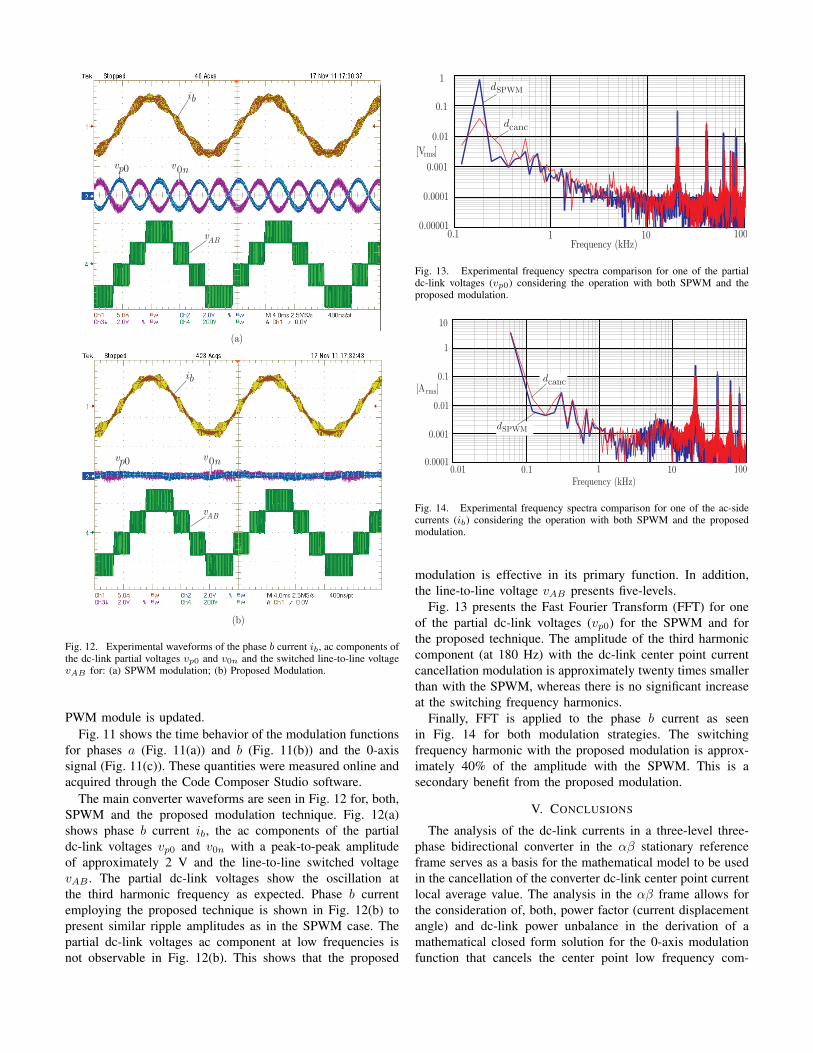
The dc-link center point current frequency spectra forthe conventional SPWM modulation and for the proposedtechnique are presented in Fig. 8. The 7.6% with respect to
400
0
-400
[A] (a)
400
0
-400
[A] (b)
(d)
0.48
-1k
0
-0.5k
[V]
1k
0.5k
380
420
410
400
390
[V] (c)
0.49 0.50 0.51 0.52
Time(s)
ia ib ic
s0
<i >s0
vp0 v0n
vAB
i
THD = 41,8% THD = 42,0%
Fig. 7. Transient behavior from a conventional PD (phase disposition) PWMmodulation to the proposed one in t = 0.50 s with αp = 0: (a) ac currents; (b)center point current; (c) dc-link voltages; and, (d) ac-side line-to-line voltage.
the fundamental ac-side phase current that is observed at thethird harmonic frequency with the SPWM is not observedwith the proposed technique. However, increased harmoniccurrent is present at the switching frequency. Two facts shouldare considered in the following. Assuming typical electrolyticcapacitors in which the equivalent series resistance dropswith frequency, the increased switching frequency currentcomponents generates lower losses. The second point is thatthere is approximately 100 A at the third harmonic withthe SPWM, whereas the current increase at the switchingfrequency is approximately 25 A. Thus, there is still advantagefrom this perspective.
The presented simulation results verify the theoretical con-siderations and show that the proposed technique is ableto fulfill the aforementioned performance requirements, i.e.,ease of implementation, operation under severe steady stateunbalance, open loop with complete elimination of the lowfrequency ripple, proper operation under wide ac-side powerfactor variation, low ac-side switched voltages distortion, good
(a)
300
200
100
400
0
[A]
0 1000 2000 3000 4000 5000
Frequency (Hz)
7.6%
78.7%
[A]
0 1000 2000 3000 4000 5000
Frequency (Hz)
(b)
90,1%300
200
100
400
0
Fig. 8. Center point current is0 frequency spectra with αp = 0: (a)conventional PD modulation; (b) proposed technique.
performance with relatively low switching frequency.
IV. EXPERIMENTAL RESULTS
The three-level bidirectional power converter presented inFig. 9 was implemented in an IGBT based lab prototype (cf.Fig. 9(b)) with a rated power of 10 kW. The experimentaltest setup comprises the following parameters: Cs = 1000µF;Vdc = 300 V; power factor PF ∼= 0.92; M = 0.8; XL =ωL = 0.1583 Ω at 60 Hz; fs = 20 kHz. The employedsemiconductors are:• IGBTs at SpX and SXn (1.2 kV / 40 A): INFINEON
IDW440N120H3• Diodes at SpX and SXn (1.2 kV / 52 A): IXYS DSEI 60• IGBTs at S0X (600 V / 30 A): IRF IRGP4PC50W• Diodes at S0X (600 V / 30 A): Fairchild ISL9R3060G2During the tests, the converter is operated as an inverter,
i.e., active power flows to the ac side and works at open loop
N
s
p
n
icsp
icsn
gpi
gni
g0i vDC
sni
s0i
gpi
p0v
0n
C
lpZL
L
L
ai
bi
ci
av
bv
v
0
sClnZ
c
v
=
Av
Bv
Cv
SpA SpB SpC
SAn SBn SCnS0C
S0B
S0A
Fig. 9. Three-phase three-level PWM converter 10 kW prototype powercircuit schematic.
feeding symmetric RL ac loads and supply by a single dc-sidepower supply.
The modulation is implemented in a Texas InstrumentsTMS320F28335 floating point DSP (32-bit CPU, 150MHz,12-bit ADC (80ns conversion rate), 6 high resolution PWM).The workflow is as follows. The modulation is initialized asa pure SPWM. The ac-side currents are then sampled and amoving average filter (four samples) stores their values, fromwhich the αβ components are extracted. The according 0-axismodulation function is computed following the rules given in(16). The cancelation signal is summed to the average valueof d0 and the respective phase modulation function and the
Gate driversAc-side inductors
DSP
Heatsink
Ac-side inductorCM choke
PCB
Gate drivers
Bus CapacitorBus Capacitor
300mm
Fig. 10. Three-level three-phase bidirectional converter prototype photograph.
-1.0
1.0
0[V]
0 π 2π
0 π 2π-1.0
1.0
0[V]
-0.3
0.3
0[V]
(a)
(b)
(c)
0 π 2πθ
θ
θ
Fig. 11. Experimental modulation signals from the DSP: (a) da; (b) db; and,(c) d0.
ib
vp0 v0n
vAB
ib
vp0 v0n
vAB
(a)
(b)
Fig. 12. Experimental waveforms of the phase b current ib, ac components ofthe dc-link partial voltages vp0 and v0n and the switched line-to-line voltagevAB for: (a) SPWM modulation; (b) Proposed Modulation.
PWM module is updated.Fig. 11 shows the time behavior of the modulation functions
for phases a (Fig. 11(a)) and b (Fig. 11(b)) and the 0-axissignal (Fig. 11(c)). These quantities were measured online andacquired through the Code Composer Studio software.
The main converter waveforms are seen in Fig. 12 for, both,SPWM and the proposed modulation technique. Fig. 12(a)shows phase b current ib, the ac components of the partialdc-link voltages vp0 and v0n with a peak-to-peak amplitudeof approximately 2 V and the line-to-line switched voltagevAB . The partial dc-link voltages show the oscillation atthe third harmonic frequency as expected. Phase b currentemploying the proposed technique is shown in Fig. 12(b) topresent similar ripple amplitudes as in the SPWM case. Thepartial dc-link voltages ac component at low frequencies isnot observable in Fig. 12(b). This shows that the proposed
Frequency (kHz)0.1 1 10 100
[V ]
0.1
0.01
0.001
0.0001
rms
0.00001
SPWM
dcanc
d1
Fig. 13. Experimental frequency spectra comparison for one of the partialdc-link voltages (vp0) considering the operation with both SPWM and theproposed modulation.
Frequency (kHz)
0.01 0.1 1 10010
10
[A ]
1
0.1
0.01
0.001
rms
0.0001
SPWMd
dcanc
Fig. 14. Experimental frequency spectra comparison for one of the ac-sidecurrents (ib) considering the operation with both SPWM and the proposedmodulation.
modulation is effective in its primary function. In addition,the line-to-line voltage vAB presents five-levels.
Fig. 13 presents the Fast Fourier Transform (FFT) for oneof the partial dc-link voltages (vp0) for the SPWM and forthe proposed technique. The amplitude of the third harmoniccomponent (at 180 Hz) with the dc-link center point currentcancellation modulation is approximately twenty times smallerthan with the SPWM, whereas there is no significant increaseat the switching frequency harmonics.
Finally, FFT is applied to the phase b current as seenin Fig. 14 for both modulation strategies. The switchingfrequency harmonic with the proposed modulation is approx-imately 40% of the amplitude with the SPWM. This is asecondary benefit from the proposed modulation.
V. CONCLUSIONS
The analysis of the dc-link currents in a three-level three-phase bidirectional converter in the αβ stationary referenceframe serves as a basis for the mathematical model to be usedin the cancellation of the converter dc-link center point currentlocal average value. The analysis in the αβ frame allows forthe consideration of, both, power factor (current displacementangle) and dc-link power unbalance in the derivation of amathematical closed form solution for the 0-axis modulationfunction that cancels the center point low frequency com-
ponents. This solution was successfully used to propose anovel straightforward modulation technique that achieves thecenter point current cancellation in a bidirectional converterthat is to be employed in modern dc bipolar distributionnetworks. Simulation and experimental results have shownthe effectivity of the proposed modulation even during loadtransient condition and compared it to conventional SPWM.The practical implementation of the technique does not requireany feedback control technique and is readily implementablein a digital control and modulation platform.
ACKNOWLEDGEMENTSThe authors would like to thank Joselito Heerdt (INEP) for
the prototype design and lending, Marcio Ortmann (INEP)for helping with the DSP code, Grover Torrico (Huawei) andRichard Moller (Infineon) for the last generation IGBTs. Theauthors also express their gratitude to the Brazilian NationalCouncil for Scientific and Technological Development (CNPq)under grant number 479982/2010-4, for the financial supportgiven in this research effort.
REFERENCES
[1] R. Teichmann and S. Bernet. A comparison of three-level convertersversus two-level converters for low-voltage drives, traction, and utilityapplications. IEEE Transactions on Industry Applications, 41(3):855–865, 2005. 0093-9994.
[2] J. Rodriguez, S. Bernet, P.K. Steimer, and I.E. Lizama. A surveyon neutral-point-clamped inverters. IEEE Transactions on IndustrialElectronics, 57(7):2219 –2230, july 2010.
[3] R. H. Baker. Bridge converter circuit, u.s. 4,270,163, 1981.[4] A. Nabae, I. Takahashi, and H. Akagi. A new neutral-point-clamped
pwm inverter. IEEE Transactions on Industry Applications, IA-17(5):518–523, sept. 1981.
[5] J.A. Heerdt, S.A. Mussa, and M.L. Heldwein. Semiconductors currentefforts and losses evaluation for single-phase three-level regenerativepwm rectifiers. In IEEE International Symposium on Industrial Elec-tronics (ISIE), pages 1046–1051. IEEE.
[6] Pradeep M. Bhagwat and V. R. Stefanovic. Generalized structure of amultilevel pwm inverter. IEEE Transactions on Industry Applications,IA-19(6):1057–1069, 1983. 0093-9994.
[7] A. I. Alolah, L. N. Hulley, and W. Shepherd. A three-phase neutralpoint clamped inverter for motor control. IEEE Transactions on PowerElectronics, 3(4):399–405, 1988. 0885-8993.
[8] T. A. Meynard, H. Foch, F. Forest, C. Turpin, F. Richardeau, L. Delmas,G. Gateau, and E. Lefeuvre. Multicell converters: derived topologies.IEEE Transactions on Industrial Electronics, 49(5):978–987, 2002.0278-0046.
[9] A. Falk, K. De Brabandere, F. Greizer, M. Victor, T. Westpahl, H. Wolf,and T. Buelo. Three-phase inverter, February 9 2009. US Patent App.12/322,897.
[10] M. Schweizer, I. Lizama, T. Friedli, and J.W. Kolar. Comparison of thechip area usage of 2-level and 3-level voltage source converter topolo-gies. In 36th IEEE Industrial Electronics Society Annual Conference(IECON 2010), pages 391–396. IEEE, 2010.
[11] S. Ogasawara and H. Akagi. Analysis of variation of neutral pointpotential in neutral-point-clamped voltage source pwm inverters. InIEEE Industry Applications Society Annual Meeting (IAS’93), pages 965–970 vol.2, October 1993.
[12] N. Celanovic and D. Boroyevich. A comprehensive study of neutral-point voltage balancing problem in three-level neutral-point-clampedvoltage source pwm inverters. IEEE Transactions on Power Electronics,15(2):242 –249, March 2000.
[13] D. Zhou and D.G. Rouaud. Experimental comparisons of spacevector neutral point balancing strategies for three-level topology. IEEETransactions on Power Electronics, 16(6):872 –879, November 2001.
[14] O. Alonso, L. Marroyo, P. Sanchis, E. Gubia, and A. Guerrero. Analysisof neutral-point voltage balancing problem in three-level neutral-point-clamped inverters with svpwm modulation. In IEEE Annual Conferenceof the Industrial Electronics Society (IECON 2002), volume 2, pages920 – 925 vol.2, nov. 2002.
[15] H. du Toit Mouton. Natural balancing of three-level neutral-point-clamped pwm inverters. IEEE Transactions on Industrial Electronics,49(5):1017 – 1025, October 2002.
[16] L. Ben-Brahim. A neutral point voltage balancing method for multi-levelgto inverters. In IEEE Industry Applications Conference (IAS 2006),volume 2, pages 959 –965, oct. 2006.
[17] J. Lago and M. Heldwein. Operation and control oriented modeling ofa power converter for current balancing and stability improvement of dcactive distribution networks. IEEE Transactions on Power Electronics(Early access), (99):1–1, 2011.
[18] K.R.M.N. Ratnayake, Y. Murai, and T. Watanabe. Novel pwm schemeto control neutral point voltage variation in three-level voltage sourceinverter. In IEEE Industry Applications Conference (IAS’99), volume 3,pages 1950 –1955 vol.3, 1999.
[19] Qiang Song, Wenhua Liu, Qingguang Yu, Xiaorong Xie, and ZhonghongWang. A neutral-point potential balancing algorithm for three-level npcinverters using analytically injected zero-sequence voltage. In IEEEApplied Power Electronics Conference and Exposition (APEC ’03),volume 1, pages 228 – 233 vol.1, feb. 2003.
[20] M. Marchesoni, P. Segarich, and E. Soressi. A new control strategy forneutral-point-clamped active rectifiers. IEEE Transactions on IndustrialElectronics, 52(2):462 – 470, 2005.
[21] J. Pou, J. Zaragoza, P. Rodriguez, S. Ceballos, V.M. Sala, R.P. Burgos,and D. Boroyevich. Fast-processing modulation strategy for the neutral-point-clamped converter with total elimination of low-frequency voltageoscillations in the neutral point. IEEE Transactions on IndustrialElectronics, 54(4):2288 –2294, aug. 2007.
[22] L. Ben-Brahim. A discontinuous pwm method for balancing the neutralpoint voltage in three-level inverter-fed variable frequency drives. IEEETransactions on Energy Conversion, 23(4):1057–1063, 2008.
[23] Q. Song, W. Liu, Q. Yu, X. Xie, and Z. Wang. A neutral-point potentialbalancing algorithm for three-level npc inverters using analyticallyinjected zero-sequence voltage. In IEEE Applied Power ElectronicsConference and Exposition (APEC’03), volume 1, pages 228–233. IEEE,2004.
[24] R. Lai, F. Wang, R. Burgos, D. Boroyevich, and D. Jiang. Averagemodeling and control design for vienna-type rectifiers considering thedc-link voltage balance. IEEE Transactions on Power Electronics,24(11):2509–2522, 2009.
[25] A. Bendre, G. Venkataramanan, D. Rosene, and V. Srinivasan. Modelingand design of a neutral-point voltage regulator for a three-level diode-clamped inverter using multiple-carrier modulation. IEEE Transactionson Industrial Electronics, 53(3):718–726, 2006.
Copyright © 2022 FDOKUMEN