Operation of HVDC converters for transformer inrush current ...
Upload
independentCategory
view
0download
0
Purdue UniversityPurdue e-Pubs
ECE Technical Reports Electrical and Computer Engineering
9-1-1996
Datapath Scheduling with Multiple SupplyVoltages and Level ConvertersMark C. JohnsonPurdue University School of Electrical and Computer Engineering
Kaushik RoyPurdue University School of Electrical and Computer Engineering
Follow this and additional works at: http://docs.lib.purdue.edu/ecetr
This document has been made available through Purdue e-Pubs, a service of the Purdue University Libraries. Please contact [email protected] foradditional information.
Johnson, Mark C. and Roy, Kaushik, "Datapath Scheduling with Multiple Supply Voltages and Level Converters" (1996). ECETechnical Reports. Paper 92.http://docs.lib.purdue.edu/ecetr/92
TR-ECE 96-16 SEPTEMBER 1996

Datapath Scheduling with Multiple Supply Voltages and Level Converters
Mark C. Johnson and Kaushik Roy School of Electrical and Computer Engineering Purdue University West Lafayette, Indiana, 47907-1 285, USA
mcjohnso @ecn.purdue.edu, [email protected] }
This research was supported in part by ARPA (F336 15-95-C- 1625), NSF CAREER award (950 1869-MIP), and ASSERT program (DAAH04-96- 1-0222)

ABSTRACT
We present an algorithm called MOVER (Multiple Operating Voltage
Energy Reduction) to minimize datapath energy dissipation through
use of multiple supply voltages. In a single voltage design, the critical
path length, clock period, and number of control steps limit minimiza-
tion of voltage and power. Multiple supply voltages permit localized
voltage reductions to take up remaining schedule slack. MOVER ini-
tially finds one minimum voltage for an entire datapath. It then de-
termines a second voltage for operations where there is still schedule
slack. New voltages can be introduced and minimized until no schedule
slack remains. MOVER was exercised for a variety of DSP datapath
examples. Energy savings ranged from 0% to 50% when comparing
dual to single voltage results. The benefit of going from two to three
voltages never exceeded 15%. Power supply costs are not reflected in
these savings, but a simple analysis shows that energy savings lcan be
achieved even with relatively inefficient DC-DC converters. Daitapath
resource requirements were found to vary greatly with respect to num-
ber of supplies. Area penalties ranged from 0% to more than 150%.
Implications of multiple voltage design for IC layout and power ;jupply
requirements are discussed.
1. IN'TRODUCTION
A great deal of current research is motivated by the need for decreased power dissi- pation while satisfying requirements for increased computing capacity. In portable systems, battery life is a primary constraint on power. However, even in non- portable systems such as scientific workstations, power is still a serious coristraint due to limits on heat dissipation.
One design technique that promises substantial power reduction is voltage scaling. The term "voltage scaling" refers to the trade-off of supply voltage against circuit area and other CMOS device parameters to achieve reduced power dissipation while maintaining circuit performance. The dominant source of power dissipation in a
conventional CMOS circuit is due to the charging and and discharging of circuit capacitances during switching. For static CMOS, the switching power is propor- tional to V& [Rabaey 19961. This relationship provides a strong incentive to lower supply voltage, especially since changes to any other design parameter can only achieve linear savings with respect to the parameter change. The penalty of volt- age reduction is a loss of circuit performance. The propagation delay of CMOS is approximately proportional to (vdd:&), [Rabaey 19961, where VT is the transistor threshold voltage.
A variety of techniques are applied to compensate for the loss of performance with respect to Vdd including reduction of threshold voltages, increasing transistor widths, optimizing the device technology for a lower supply voltage, and shortening critical paths in the data path by means of parallel architectures and pipelining.
Data path designs can benefit from voltage scaling even without changes in device technologies. Algorithm transformations and scheduling techniques can be used to increase the latency available for some or all data path operations. The increased latency allows an operation to execute at a lower supply voltage without violating schedule constraints. "Architecture-Driven Voltage Scaling" is a name applied to this approach.
A number of researchers have developed systems or proposed methods that incor- porate architecture driven voltage scaling [Chandrakasan et al. 1995; Raghunathan and Jha 1994; Raghunathan and Jha 1995; Goodby et al. 1994; Kumar et al. 1995; SanMartin and Knight 1995; Raje and Sarrafzadeh 1995; Gebotys 1995al. HYPER- LP [Chandrakasan et al. 19951 is a system that applies transformations to the data flow graph of an algorithm to optimize it for low power. Other systems accept the algorithm as given and apply a variety of techniques during scheduling, module selection, resource binding, etc. to minimize power dissipation. All of the systems mentioned above try to exploit parallelism in the algorithm to shorten critical paths so that reduced supply voltages can be used. Most systems [Chandrakasan et al. 1995; Raghunathan and Jha 1994; Raghunathan and Jha 1995; Goodby et al. 1994; Kumar et al. 1995; Gebotys 1995al also minimize switched capacitance in the data path.
Most voltage scaling approaches require that the IC operate at a single supply voltage. Although substantial energy savings can be realized with a single minimum supply voltage, one cannot always take full advantage of available schedule slack to reduce the voltage. Non-uniform path lengths, a fixed clock period, andl a fixed number of control steps can all result in schedule slack that is not fully exploited. Figure 1 provides examples of each type of bottleneck. When there are non-uniform path lengths, the critical (longest) path determines the minimum supply voltage even though the shorter path could execute a t a still lower voltage and meet timing constraints. When the clock period is a bottleneck, some operations only use part of a clock period. The slack within these clock periods goes to waste. Additional voltages would permit such operations to use the entire clock period. Finally, a fixed number of control steps (resulting from a fixed clock period and latency constraint) may lead to unused clock cycles if the sequence of operations cloes not match the number of available clock cycles. This could even occur in the critical path. Consider the control step bottleneck illustrated in figure 1. Decreasing the supply voltage would cause the datapath latency to increase from three to six clock

cycles. Unless the clock period can be changed, the datapath cannot be scaled to four clock cycles. Additional voltages would allow specific operatior~s to be slowed down to take up unused cycles. It should be noted that in some cases these bottlenecks can be alleviated by restructuring the datapath specification or choosing alternate circuit implementations for some operations.
Clock Cycle
0 -
Unused Slack
Unused Slack
Unused
Non-Uniform Path LenGh
Clock Period
Number of'
Control St'eps
Fig. 1. Examples of scheduling bottlenecks
Literature on multiple voltage synthesis is limited, but this is changing. Publica- tions that address the topic include [Raje and Sarrafzadeh 19951, [Gebotys 1995a], and [Johnson and Roy 19961. Raje and Sarrafzadeh [Raje and Sarrafzadeh 19951 schedule the data path and assign voltages to data path operators so as to mini- mize power given a predetermined set of supply voltages. Logic level conversions are not explicitly modeled in their formulation. Gebotys [Gebotys 1995a] used an integer programming approach to scheduling and partitioning a VLSI system across multiple chips operating at different supply voltages. Johnson [Johnson and Roy 19961 used an integer program to choose voltages from a list of candidatec,, sched- ule datapath operations, model logic level conversions, and assign voltages to each operation.
The integer linear program (ILP) presented in [Johnson and Roy 19961 led to the MOVER algorithm to be discussed in this paper. The purely ILP approach was useful because it allowed us to test the problem formulation and obtain provably optimal solutions using a general purpose branch and bound ILP solver. Execution times varied from minutes to days. However, for certain well defined problems, ILP can in fact be very efficient. Gebotys [Gebotys 19921 has shown that for the gen- eral precedence constrained scheduling problem, one can specify linear constraints on continuous variables that very closely approximate the boundary of the set of integer solutions. This is a very desirable property because it allows a branch and bound algorithm to finish in a small number of iterations. A difficulty with the ILP approach is that there may be subproblems for which it is very difficult to obtain such tight linear constraints. This often leads to very large execution times. Mod- eling of logic level conversions proved to be especially difficult in terms of decision variables and constraints.
MOVER attempts to use ILP only to solve those subproblems for which an effi- cient formulation is known. particular, ILP is used to partition operations into high
and low voltage groups and to evaluate schedule feasibility for particular choices of supply voltages. MOVER searches a user specified range of supply voltages, calling the ILP formulation as needed to evaluate schedule feasibility and obtain a11 energy estimate. In the remainder of this paper, we will describe the MOVER algorithm, explain the delay and energy dissipation models, discuss IC layout and power sup- ply considerations, present scheduling results for several datapath specifi~cations, make observations and draw conclusions regarding multiple voltage datapaths and the applicability of this algorithm.
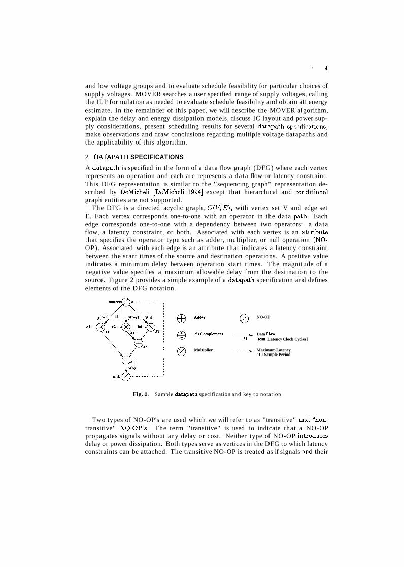
2. DATAPATH SPECIFICATIONS
A datapath is specified in the form of a data flow graph (DFG) where each vertex represents an operation and each arc represents a data flow or latency constraint. This DFG representation is similar to the "sequencing graph" representation de- scribed by DeMicheli [DeMicheli 19941 except that hierarchical and cortditional graph entities are not supported.
The DFG is a directed acyclic graph, G(V, E ) , with vertex set V and edge set E. Each vertex corresponds one-to-one with an operator in the data path. Each edge corresponds one-to-one with a dependency between two operators: a data flow, a latency constraint, or both. Associated with each vertex is an aktribute that specifies the operator type such as adder, multiplier, or null operation (NO- OP). Associated with each edge is an attribute that indicates a latency constraint between the start times of the source and destination operations. A positive value indicates a minimum delay between operation start times. The magnitude of a negative value specifies a maximum allowable delay from the destination to the source. Figure 2 provides a simple example of a datapath specification and defines elements of the DFG notation.
@ NO-OP
> Data Flow [I] Win. Latency Clock Cycles]
j @ Multiplier .........., Maximum Latency of 1 Sample Period
Fig. 2. Sample datapath specification and key t o notation
Two types of NO-OP's are used which we will refer to as "transitive" and "non- transitive" NO-OP's. The term "transitive" is used to indicate that a NO-OP propagates signals without any delay or cost. Neither type of NO-OP in1;roduces delay or power dissipation. Both types serve as vertices in the DFG to which latency constraints can be attached. The transitive NO-OP is treated as if signals and their
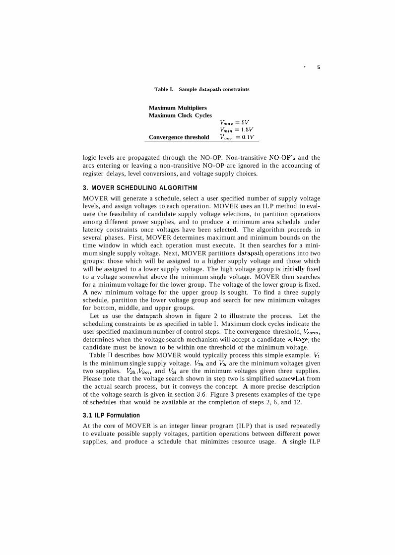
Table I. Sample datapath constraints
Maximum Multipliers Maximum Clock Cycles
v,,, = 5 v V,,, = l.5V
Convergence threshold VconV = 0.lV
logic levels are propagated through the NO-OP. Non-transitive NO-OP's and the arcs entering or leaving a non-transitive NO-OP are ignored in the accounting of register delays, level conversions, and voltage supply choices.
3. MOVER SCHEDULING ALGORITHM
MOVER will generate a schedule, select a user specified number of supply voltage levels, and assign voltages to each operation. MOVER uses an ILP method to eval- uate the feasibility of candidate supply voltage selections, to partition operations among different power supplies, and to produce a minimum area schedule under latency constraints once voltages have been selected. The algorithm proceeds in several phases. First, MOVER determines maximum and minimum bounds on the time window in which each operation must execute. It then searches for a mini- mum single supply voltage. Next, MOVER partitions datapath operations into two groups: those which will be assigned to a higher supply voltage and those which will be assigned to a lower supply voltage. The high voltage group is initia.11~ fixed to a voltage somewhat above the minimum single voltage. MOVER then searches for a minimum voltage for the lower group. The voltage of the lower group is fixed. A new minimum voltage for the upper group is sought. To find a three supply schedule, partition the lower voltage group and search for new minimum voltages for bottom, middle, and upper groups.
Let us use the datapath shown in figure 2 to illustrate the process. Let the scheduling constraints be as specified in table I. Maximum clock cycles indicate the user specified maximum number of control steps. The convergence threshold, V,,,, , determines when the voltage search mechanism will accept a candidate vol1,age; the candidate must be known to be within one threshold of the minimum voltage.
Table I1 describes how MOVER would typically process this simple example. Vl is the minimum single supply voltage. V2h and Vzl are the minimum voltages given two supplies. V3h,V3mr and V3( are the minimum voltages given three supplies. Please note that the voltage search shown in step two is simplified somewllat from the actual search process, but it conveys the concept. A more precise description of the voltage search is given in section 3.6. Figure 3 presents examples of the type of schedules that would be available a t the completion of steps 2, 6, and 12.
3.1 ILP Formulation
At the core of MOVER is an integer linear program (ILP) that is used repeatedly t o evaluate possible supply voltages, partition operations between different power supplies, and produce a schedule that minimizes resource usage. A single ILP

Table 11. MOVER Scheduling Example
1. Determine maximum range of X 1 E [l, 41, X 2 E [O, 31, X 3 E [O, 31 start times for each operation A1 E [ l , 41, A2 E [2,5] by generating an as soon as possible (ASAP) schedule and an as late as possible (ALAP) schedule.
2. Search for minimum single supply K,,t feasible? Vhi K O Initial condition 5V 1.5V 1st Candidate voltage 3.3V No 5V 3.3V Infeasible, so try higher 4.1V Yes 4.1V 3.3V Feasible, so try lower 3.7V Yes 3.7V 3.3V Feasible, so try lower 3.5V No 3.7V 3.5V Infeasible, try higher 3.6V Yes 3.6V 3.5V Vhl - KO < Vconv
So let Vl = 3.6V
3. Partition operations between two High voltage operations: ~ 1 , ~ 2 - power supplies Low voltage operations: Xl,X2, X3
4. Insert logic level conversions Level conversions required between into delay and energy model. X1 and A2, X2 and Al , X3 and A1 --
5. Temporarily fix high voltage v2h = x (Vma, +Vl)
6. Search for minimum lower supply Vm,,, 5 V21 5 Vl in same manner as step 2 ~ e s u l t y &l = 2.4 and then fix that voltage
7. Search for minimum higher Vzr 5 V2h 5 previousvzh supply and fix voltages Result: V2h = 3.7V
8. Partition operations from lower Operations in top group (A~,AZ.) - -
group into middle (V&,,) unchanged. and bottom (V31) voltage Middle group: X 1,X2. groups. Bottom Group: X3.
9. Insert logic level conversions No new logic level conversions into delay and energy model required in this example.
10. Temporarily fix top voltage V3h = $ X (Vma~ + V2h)
11. Temporarily fix middle voltage Km =
12. Search for minimum low supply Result: v3l = 1.9V
13. Search for min. middle supply Result: = 2.5V
14. Search for minimum top supply Result: V3h = 3.8V

Clock Cycle (Step 6) (Step 12)
2 Supplies 3 Supplies
Fig. 3. Sample Schedules
formulation serves all three purposes. In each case, MOVER analyzes the DFG and generates a collection of linear inequalities that represent precedence constraints, timing constraints, and resource constraints for the datapath to be scheduled. A weighted sum of the energy dissipation for each operation is used as the optiimization objective when partitioning operations or evaluating the feasibility of a supply voltage. A weighted sum of resource usage serves as the optimization objective when minimizing resources. The inequalities and objective function are packed into a matrix of coefficients that are fed into an ILP program solver (CPLEX). MOVER interprets the results from CPLEX and annotates the DFG to indicate schedule times and voltage assignments.
The architectural model assumed by MOVER is depicted in Figure 4. All op- erator outputs have registers. Each operator output feeds only one register. That register operates a t the same voltage as the operator supplying its input. All level conversions, when needed, are performed at operator inputs.
operator + operator register level operator
converter
Fig. 4. MOVER architectural model
MOVER'S ILP formulation works on a DFG where voltage assignments for some operations may already be fixed. For operations not already fixed to a voltage,
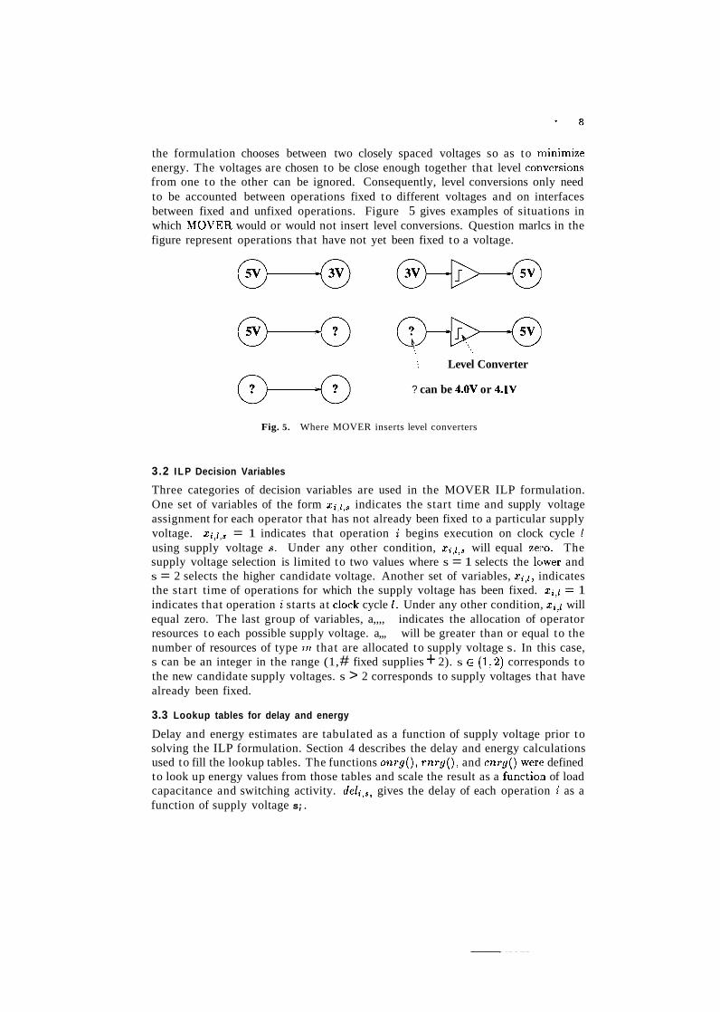
the formulation chooses between two closely spaced voltages so as to minimize energy. The voltages are chosen to be close enough together that level con.versions from one to the other can be ignored. Consequently, level conversions only need to be accounted between operations fixed to different voltages and on interfaces between fixed and unfixed operations. Figure 5 gives examples of situations in which MOVER would or would not insert level conversions. Question marlcs in the figure represent operations that have not yet been fixed to a voltage.
: Level Converter
? can be 4.OV or 4.1V
Fig. 5. Where MOVER inserts level converters
3.2 ILP Decision Variables
Three categories of decision variables are used in the MOVER ILP formulation. One set of variables of the form xi,l, , indicates the start time and supply voltage assignment for each operator that has not already been fixed to a particular supply voltage. xi ,[ , , = 1 indicates that operation i begins execution on clock cycle I using supply voltage s. Under any other condition, xi,l,, will equal zero. The supply voltage selection is limited to two values where s = 1 selects the lower and s = 2 selects the higher candidate voltage. Another set of variables, xi,^, indicates the start time of operations for which the supply voltage has been fixed. xi,l = 1 indicates that operation i starts a t clock cycle 1. Under any other condition, xi,/ will equal zero. The last group of variables, a,,,, indicates the allocation of operator resources to each possible supply voltage. a,,, will be greater than or equal to the number of resources of type rn that are allocated to supply voltage s. In this case, s can be an integer in the range (1, # fixed supplies + 2). s E (1,2) corresponds to the new candidate supply voltages. s > 2 corresponds to supply voltages that have already been fixed.
3.3 Lookup tables for delay and energy
Delay and energy estimates are tabulated as a function of supply voltage prior to solving the ILP formulation. Section 4 describes the delay and energy calculations used to fill the lookup tables. The functions onrg(), rnrg() , and cnrg() were defined to look up energy values from those tables and scale the result as a functioin of load capacitance and switching activity. deli,,, gives the delay of each operation i as a function of supply voltage s;.

onrg(j, s j , cload) returns the energy estimate for operation j, using suplply volt- age s j , with a load capacitance of cload at the output. rnrg(sj, fanoutj) returns the energy estimate for a register using supply voltage s j and an output load ca- pacitance of fanoutj. janoutj reflects the level of fanout from operation j in the DFG. cnrg(si, s j , cj) returns the energy estimate for a level conversion froni a block operating at supply voltage si to a block operating at supply voltage s j . cj is the input capacitance of operation j. deli,,, gives the delay of operation i including register propagation and level conversion delays.
3.4 Objective Functions
The objective function (equation 1) estimates the energy required for one execution of the data path as a function of the voltage assigned to each operation. Consider the energy expression split into two parts. The first nested summation counts the total energy contribution associated with operations not already fixed to a supply voltage. The second nested summation counts the total energy contribution of operations that are already fixed to a particular supply voltage.
For each operation j that has not been fixed to a supply voltage (e.g., j E Vfree), the first nested summation accumulates the energy of operation j (onrg(j, s j , creg)), the register at the output of operation j (rnrg(sj, fanoutj)), and any level conver- sions required at the input to j (cnrgfree(j, s)) . The decision variables ,cj,r,, are used to select which lookup table values for operator, register, and level conversion energy are added into the total energy. We must sum over both candidate supply voltages s j and all clock cycles I in the possible execution time window Rj of opera- tion j . E,,,, is the set of DFG arcs that may require a level conversion, depending on voltage assignments. Voper is the set of DFG vertices that are not NO-OPs. biz is the set of DFG vertices (operations) that have been fixed to a particular voltage. Q,,, is the set of vertices that have not previously been fixed to a voltagl?.
For each operation j that has been fixed to a supply voltage, we again accumulate the energy of each operation, register, and level conversion. The only difference from the expression for free operations is that now all voltages in the expression are constants determined prior to solving the ILP formulation. Consequently, the index s j can be removed from the summation and the decision variable x.
Energy = 2
C C C xj,r,s X (onrg(j1 US I creg) + rnrg(u,, cf anout(i)) + cnr,yf .,,(j, s)) jEVfre.nVOp,, IER, S=I
cnrg ,,,(j, S) and cnrg f i x (j) represent the level conversion energy at the input of free and fixed operations respectively.
cnrgfree(j, s ) = C cnrg(vi, us, ci,,) + C cnrg(u1, U S , tin,) il(i,j)EE,.,, and iEVf,, il(i,j)EE,,,, and i E V f r e e
cnrgji=(j) = C cnrg(vi, v j , tin,) + C cnrg(v1. ujl cin1) i l( i , j )EEcon, and iEVI,, il(i,j)EEcon, and iEVfree
(3)
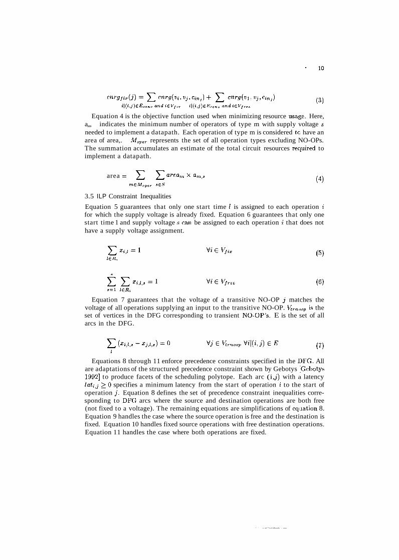
Equation 4 is the objective function used when minimizing resource usage. Here, a,,, indicates the minimum number of operators of type m with supply voltage s needed to implement a datapath. Each operation of type m is considered ta have an area of area,. Moper represents the set of all operation types excluding NO-OPs. The summation accumulates an estimate of the total circuit resources required to implement a datapath.
area = C C aream x amB,
3.5 ILP Constraint Inequalities
Equation 5 guarantees that only one start time 1 is assigned to each operation i for which the supply voltage is already fixed. Equation 6 guarantees that only one start time 1 and supply voltage s can be assigned to each operation i that does not have a supply voltage assignment.
Equation 7 guarantees that the voltage of a transitive NO-OP j matches the voltage of all operations supplying an input to the transitive NO-OP. &rn,,op is the set of vertices in the DFG corresponding to transient NO-OP's. E is the set of all arcs in the DFG.
Equations 8 through 11 enforce precedence constraints specified in the IIFG. All are adaptations of the structured precedence constraint shown by Gebotys 1:Gebotys 19921 to produce facets of the scheduling polytope. Each arc (i, j) with a latency lati , j 2 0 specifies a minimum latency from the start of operation i to the start of operation j . Equation 8 defines the set of precedence constraint inequalities corre- sponding to DFG arcs where the source and destination operations are both free (not fixed to a voltage). The remaining equations are simplifications of equation 8. Equation 9 handles the case where the source operation is free and the destination is fixed. Equation 10 handles fixed source operations with free destination operations. Equation 11 handles the case where both operations are fixed.

del,,,, +l m a x c l k
s l = l l1=0 l2=1
del,,.. +I m a x c l k
2 del,,.,+l m a x c l k
del,,.. +l m a x c l k
Vi, j E Vfiz, Vl E L, V(i, j ) I lati , j 2 0
Equations 12 through 15 enforce maximum constraints specified in the DFG. Each arc (i, j ) with a latency latiIj < 0 specifies a maximum delay from operation j to operation i. Equation 12 defines the set of maximum latency constraint in- equalities corresponding to arcs where the source and destination ~perat~ions are both free (not fixed to a voltage). The remaining equations are simplifications of equation 12. Equation 13 handles the case where the source operation is free and the destination is fixed. Equation 14 handles fixed source operations with free destination operations. Equation 15 handles the case where both operat,ions are fixed.
2 2 m a x c l k
Vi, j E V j r e e Vl E L, V(i, j ) I lati , j < 0
2 m a x c l k

2 maxelk
tli E Vfix, t l j E VVfree tll E L, tl(i, j) I l ~ t i , ~ < 0
maxelk
x j , l + C xi,r2 5 1
Equations 16 and 17 ensure that resource usage during each time step does not exceed the resource allocation given by am,, . The expressions on the left computes the number operations of type m with supply voltage s that are executing concur- rently during clock cycle I. am,, indicates the number of type m resources that have been allocated to supply voltage s. Equation 16 enforces the resource constraint for free operations. Equation 17 enforces the constraint for fixed operations. Free operations are allowed to take on one of two candidate voltages.
tlm E Moper, tll E L, tlsi E (1,2)
C C xi,ll 5 am,s, i I iEV f ix, type(i)=m, supply(i)=s, ll=l-del,,,, +l
Equation 18 enforces the user specified resource constraints. mazres(n;~) repre- sents the total number of resources of type m (regardless of voltage) thai; can be permitted. The left side expression accumulates the number of resources of type m that have been allocated to all supply voltages. The total is not allowed to exceed the user specified number of resources.
C a m t 3 5 maxres(m) tlm E Moper 3 E S
3.6 Voltage search
MOVER searches a continuous range of voltages when seeking a minimu~r~ voltage one, two, or three power supply design. The user must specify a convergence

Table 111. Voltage search algorithm
I 1. Choose starting voltages V2 and Vl = V2 - V,,,, where V,,, < V2 5 V,;,
2. Create matrix of ILP constraint inequalities. 3. Obtain minimum energy soIution to inequalities.
The solution will provide a schedule, a mapping of Vl or V2 to each operator, an energy estimate, and an area estimate for the datapath.
4. If a solution was found, then 4a. If most operations were assigned to Vl, then
Choose new candidate voltages midway between Vl and KO. Set Vh, = V2. Go to step 2.
4b. else There must be little or no benefit to assigning operations to VI
Fix all operations to V2 DONE!
4c. else (if the problem was infeasible) Choose new candidate voltages midway between l4 and Vh;. Set KO = V2 Go t,n den 2 .
threshold Vconu that is used to determine when a voltage select,ion is acceptably close to minimum. Let Vhi and KO represent the current upper and lower bound on the supply voltage (as in table 11). The initial values of Vhi and KO will1 be set as described in table 11.
When searching for a minimum single supply voltage, all operations are initially considered to be free (not fixed to a voltage). When searching for a minimumset of two or three supply voltages, MOVER considers one power supply at a time. The voltage will be fixed for any operations not allocated to the supply voltage under consideration. Table I11 outlines the voltage search algorithm.
3.7 Partitioning
Partitioning is the process by which MOVER takes all free operations in the DFG and allocates each to one of two possible power supplies. Partitioning is not per- formed until a single minimum supply voltage is known for the group of operations. Let Vl represent the minimum supply voltage for the free operations. Choose two candidate supply voltages (V, and Vb) one slightly above Vl and the other. slightly below.
vconu v, = Vl - - 2
Set up the ILP constraint inequalities. Obtain a minimum energy schedule. Operations will only be assigned to V, if there is schedule slack available. There may be several ways that the operations can be partitioned. In such a case, the optimal ILP solution will maximize the energy dissipation of the lower vo1ta:ge group (i.e., put the most energy hungry operations in the lower voltage group). 'Phis will tend to maximize the benefit from reducing the voltage of the lower group.
Given a successful partition, operations assigned to Va will be put into the lower supply voltage group and operations assigned to Vb will be put into t h l~ higher supply voltage group. Let count(V,) represent the number of operations a.llocated to voltage V,. Let MinPar t i t ion represent the user specified minimum allocation ratio for a successful partition. Then the partition is considered successful if the following two conditions are satisfied:
count (V,) > MinPar t i t ion count(V,) + count(Vb) -
count (V,) < 1
count(Va) + count(Vb)
The partition can fail at least three ways.
(1) All operations were allocated to the lower supply voltage. (2) All or nearly all operations were allocated to the higher supply voltage. (3) The ILP solver exceeded some resource or time limit.
The first situation indicates that the minimum single voltage could have been a bit lower. In this event, MOVER lowers the values of V, and by and tries the partition again. Lowering Va and Vb too far will lead to a completely infeasible ILP problem. The second situation indicates that there is not enough schedule slack available for any operations to bear a further reduction in voltage. In this case, MOVER terminates. The only remedies for the third situation are to either increase resource and time limits on the ILP solver or make the problem smaller.
4. CHARACTERIZATION OF DATAPATH RESOLIRCES
The results presented in this paper make use of four types of circuit resources: an adder, multiplier, register, and level converter. MOVER requires models of the energy and delay of each type of resource as a function of supply voltage, load capacitance, and average switching activity. The input capacitance of each resource type is required in order to determine load capacitances within a dlatapath design. For each type of resource, an HSPICE netlist was created. 0.8 micron MOSIS library models were used with the level 3 MOS transistor model. Energy dissipation and worst case delays were measured from simulation results. Energy dissipation is assumed to scale proportionally to input switching activity. Input capacitance in each case was determined by inserting a series resistance .at input nodes and then measuring input rise time in response to a step function. The results of all measurements were used to compute model parameters pro.vided as

Table IV. Nominal energy and delay values used by MOVER
I Resource I Energy I -$ Energy I Delay I $ Delay I C,, I
input to MOVER. In this section we will discuss the particulars of how the delay and energy characteristics of each resource type were measured and modeled with respect to supply voltage and load capacitance.
Type ADDER MULTIPLIER REGISTER
4 .1 Data path operators and registers
16 bit adders and multipliers were simulated with a supply voltage of 5V, average input switching activities of 50% and a nominal load capacitance of O.lpF on each output pin. Total average power dissipation was measured. The average energy per clock cycle was then computed and provided as input to MOVER. Registers were characterized in a similar manner, except that a single bit register was simulated for a few clock cycles. The register energy dissipation was then scaled to represent 16 bit, 50% switching activity conditions. Worst propagation delays through the adder and multiplier were measured at 5V supply and O.lpF load on each output. Delays were also measured at 0.2pF load in order to measure the scaling of delay with respect to load. Delay is modeled as scaling linearly with respect to the load capacitance.
Power dissipation (E) for each operator and register scales with respect to supply voltage as
where Eo is the energy dissipation of the operator or register measured at the nominal supply voltage Vo.
Delay ( tp) for each operator and register scale with respect to supply voltage as
[PJI 84 2966 312
where tp, is the propagation delay measured at the nominal supply voltage Vo. The power and delay scaling factors were derived directly from the CMOS power and delay equations described by Rabaey [Rabaey 19961.
Table IV gives the model parameters used by MOVER for each type of resource. Note that the register delay given here is just the propagation time relative to a clock edge. Register setup time is treated as part of the datapath operator delays. The nominal values are for VDD = 5V, C L ~ ~ ~ = O.lpF, 16 bit wide operations, and input switching activities of 50%. Energy values are given as the average per clock cycle.
KJIPFI 200 200 200
[nsl 12.0 18.5 0.48
G/PFI 3.5 3.33 2.25
[PFI 0.021 0.095 0.045
4.2 Level conversion
Whenever one resource has to drive an input of another resource operating a t a higher voltage, a level conversion is needed at the interface. Four alternatives were considered to accomplish this: omit the level converter, use a chain of inverters a t successively higher voltages, use an active or passive pullup, or use a dual cascode voltage switch (DCVS) circuit as a level converter [Chandrakasan et al. 1994; Usami and Horowitz 19951. We omit the level converter for stepdown conversions and use the DCVS circuit for s t epup conversions. Given appropriate transistor sizes, this circuit exhibits no static current paths and it can operate over a full 1.5V to 5.OV range of input and output supply voltages.
VOUTB r\ VOUT \,
v1
IN MZN
MIN
- -
M3N All transistors 0 . 8 ~ length and 4 . 0 ~ width except where noted
- -
Fig. 6. DCVS Level Converter
Another option is to combine the register and level converters together. This approach was documented by Usami and Horowitz [Usami and Horowitz 19951. The combined register and level conversion was found to dissipate only 10% more power than the register alone.
A model was needed that could accurately indicate the power dissipation and propagation delay of the DCVS level converter as a function of the input logic supply voltage Vl, output logic supply voltage Vz, and load capacitance. Th~e circuit was studied both analytically and from HSPICE simulation results to determine a suitable form for the model equations. Coefficients of the equations were then calibrated so that the model equations would produce families of curves closely matching simulation results for Vl ranging from 1.5V to 5V and Vl +VT 5 Tfz 5 5V. These are the ranges of supply voltages for which a level converter is needed. Typical energy dissipation of the level converter was found to be on the order of 5 to 15pJ per switching event per bit, given a O.lpF load. Typical propagation delays range were approximately Ins for level conversions such as 3.3V to 5V or 2.4V to 3.3V.
Propagation delays become large as the input voltage of the level converter falls towards 2VT. A 2.5V to 5V conversion had a delay of about 2.5ns. A 2V to 5V conversion had a delay of nearly 5ns.
4.2.1 Power Dissipation Model. The power dissipation model is separa.ted into three factors. The first factor calculates the power consumption for V1 = V2. Charging and discharging of the load capacitance contributes a vZ2 ternn to the power. The short circuit current on the paths through MlP/MlN and M:!P/M2N contribute power as a third order polynomial of V2.
D C V S P WR(V2, Vz) = (25)
The coefficients a 3 through a 0 are obtained by means of a polynomial curve fit t o a plot of circuit power vs. V2.
The next factor estimates the ratio of increase in power consumption due to Vl being less than V2.
bO represents the portion of power dissipation not affected by Vl. The fractional expression models the effect of Vl < V2. When Vl < V2, M2N is in saturation until VoUT drops to V2 - VT. Shortly thereafter, the cross-coupled circuit switches and M2P turns off. The fractional expression in DCVSPWR(V1, V2) models the effect of saturation current in the pull-down transistors on the duration of short circuit current. The final term represents the power consumption in the inverter.
The power model is scaled linearly for load capacitance. All of the ainalytical expressions for DCVS power dissipation showed a linear dependence on load ca- pacitance. Plots of power dissipation versus load capacitance showed an almost perfect linear dependence on the load. Furthermore, if one chooses a nominal load capacitance (CLo) to evaluate power dissipation, the slope of power versus capaci- tance is found to be proportional to the power dissipation (pwr0) at the nominal load. dpdc is the slope of power versus capacitance for the values of Vl and V2 for which pwrO was measured. The following expression models this dependence on load capacitance.
(CL - CLO) DCVSPWR(V1 , V2) x ( 1 + dpdc x pwrO )
4.3 Delay Model
The delay model hinges on the following observation of delay versus V2 -For fixed values of Vl. For V2 > Vl + VT, delay increases almost linearly with respect to V2. More importantly, the delay versus V2 lines all intersect a t nearly the sarne point on a graph. To take advantage of this behavior, a polynomial curve fit to ,& was used to estimate the position of a point on the linear portion of each delay versus Vz curve. In particular, data points corresponding to V2 = Vl + VT were used. The expression for DCVSDEL(Vl, Vl + VT) estimates these data points.
The expression for DCVSDEL(Vl, V2) models the radial behavior of the delay versus Vz curves. (Vo, deEO) specifies the point from which the lines radiate.
DCVSDEL(V1, Vl + VT) - deEO x (V2 - Vo) + deEO
Vi + VT - Vo
Delay scales with respect to load capacitance in a manner identical to that de- scribed for power versus capacitance.
5. RESULTS
5.1 Datapath examples
ILP schedule optimization results are presented for six example data pathis: a four point F F T (FFT4), the 5th order elliptic wave filter benchmark (ELLIP) [Rao 19921, a 6th order Auto-Regressive Lattice filter (LATTICE), a frequency sampled filter (FSAMP) with three 2nd order stages and one 1st order stage, a direct form 9 t ap linear phase FIR filter (LFIRS), and a 5th order state-space realization of an IIR filter (SSIIR). In the F F T data path, complex signal paths are split into real and imaginary data flows. For all other data paths, the signals are modeled as non- complex integer values. All data flows were taken to be 16 bits wide. Switching activities a t all nodes were assumed to be 50%, i.e., the probability of a transition on any selected 1 bit signal is 50% in any one sample interval.
Each example was modeled for one sample period with data flow and latency constraints specified for any feedback signals. No conditional operations were mod- eled. Any loops that start and finish within the same sample period were completely unrolled. Any loops spanning multiple sample periods were broken. A data flow passing from one sample period to the next was represented by input and and out- put nodes in the DFG connected by a backward arc to specify a maximuni latency
constraint from the input to the output. A 20ns clock was specified for all e:iamples. Latency constraints were specified so that the data introduction interval equals the maximum delay from the input to the output of the data path.
5.2 M O V E R Results
The MOVER algorithm was exercised for each datapath topology (FFT4., ELLIP, LATTICE, FSAMP, LFIR9, and SSIIR) under a variety of latency and resource constraints.
Figure 7 presents energy reduction results. The left-most column identifies the particular datapath topology and indicates the number of operations (additions, multiplications, and sample period delays) performed in one iteration of the data- path. "Max Lat/Clks" specifies the maximum latency (equal to the data sample rate) and the maximum number of control steps (Clks), both given in ternns of the number of clock cycles. "Max +/-" specifies the maximum numbers of adder and multiplier circuits permitted in the design. Values of "-/-" indicate that unlim- ited resources were permitted. The columns headed by "Voltages 1 2 3" indicate the supply voltages selected by MOVER. A "-" is used to fill voltage columns "2" or "3" in those cases where a one or two supply voltage result is presented. The string " N R in voltage columns "1" and "2" indicates that a solution with two supply voltages could not be obtained. " N R in all three columns indicates that a solution with three supply voltages could not be obtained. The "Exec" column re- ports the minutes of execution time (Real, not CPU) required to obtain th~e result. The number in parenthesis identifies the type of machine used to obtain the result. "(1)" indicates a SPARCserver 1000 with 4 processors and 320MB of RAM. "(2)" indicates a Sparc 5 with 64MB of RAM.
The bar graph down the center represents the normalized energy consuniption of each test case. Each energy result is divided by the single supply voltage, unlimited resource, minimum latency result to obtain a normalized value. Single supply voltage results are shown with black bars. All other results are shown in gray. This style of presentation is intended to visually emphasize the effect of different latency, resource, and supply voltage constraints on the energy estimate. The right-most column presents the absolute energy estimate in units of 10-12 Joules (pdl).
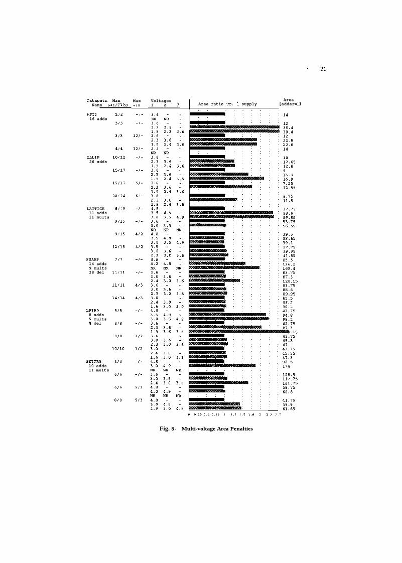
Figure 8 presents area penalty results. All but two columns have the same mean- ing as the corresponding columns in figure 7. The only exceptions are the bar graph and the "area" column on the right. The "area" value is a weighted sum of the min- imum circuit resources required to implement the datapath schedule. The resources (all 16 bits wide) were weighted as follows: adder=l, multiplier=16, register=0.75, and level converter=0.15. These weights are proportional to the transistor count of each resource. Each area value was divided by the area estimate for the corre- sponding single voltage result. Each single voltage result is shown as a bllack bar. Two and three voltage results are shown in gray.
5.3 Observations
The preceding results permit several observations to be made regarding the effect of latency, circuit resource, and supply voltage constraints on energy savings, area costs, and execution time. Because our primary objective has been to minimize energy dissipation through use of multiple voltages, we are especially interested in

FFT4 1 6 a d d s
D a t a p a t h Max Max V o l t a g e s E x e c l h o s t l EnerW vs. herW
ELL1 P 2 6 a d d s
Name L a t l C l k s c l x 1 2 3 [min]
LATTICE 1 1 a d d s 1 1 m u l t s
Min L a t . , U n l i m . R e s o u r c e s [pJI
FSAMP 1 4 a d d s 9 m u l t s 38 d e l
LFIR9 8 a d d s 5 m u l t S 8 d e l
SSIIR5 10 a d d s 11 m u l t s
Fig. 7. Multi-voltage Energy Savings
Datapath Name L
Max ,at/Clks
Max + / X
Voltages 1 2
Area 3 1 Area ratio vs. 1 supply [adder= 11
FPT4 16 adds
ELLIP 26 adds
LATTICE 11 adds 11 mults
FSAMP 14 adds 9 mults 38 del
LPIR9 8 adds 5 mults 8 del
SSIIR5 10 adds 11 mults
Fig. 8 8. Multi-voltage Area Penalties
the comparison of multiple supply voltage results to minimum single supply voltage results. Energy savings ranging from 0% to 50% were observed when comparing multiple to single voltage results. Estimated area penalties ranged from a slight improvement to a 170% increase in area. Actual area penalties could be higher, since our estimate only considers the number of circuit resources used. There is not a clear correlation between energy savings and area penalty when looking at the complete set of results. Sometimes a substantial energy savings was achieved with minimal increased circuit resources, other times even a small energy savings incurred a large area cost.
If we consider the impact of latency constraints alone, effects on area an,d energy are easier to observe. In most cases, multiple voltage area penalties were greatest for the minimum latency unlimited resource test cases. We can also observe that increasing latency constraints always led to the same or lower energy for a given number of supply voltages. However, the effect of latency constraints on the single vs. multiple voltage trade-off varied greatly from one example to another. Results for multiple voltages are most favorable in situations where the single supply volt- age solution did not benefit from increased latency, perhaps due to a control step bottleneck such as illustrated earlier in figure 1.
The effect of resource constraints on energy savings are also relatively easy to observe. Not surprisingly, resource constraints tended to produce the lowest area penalties. The only reason for any area penalty at all in the resource conistrained case is that sometimes the minimum single supply solution does not require all of the resources that were permitted. Tightening resource constraints always led to energy estimates that were either the same or worse than the corresponding unlimited resource case.
Program execution time was affected most by the latency, control step, and resource constraints. 40% of the minimum voltage (1, 2, and 3 supply) schedules were obtained in a minute or less. 93% of the results were obtained in 10 minutes or less. The remaining 7% took anywhere from 37 to 101 minutes. All of execution times less than a minute occurred for test cases with 10 or fewer control steps. The largest execution times occurred for test cases where resource constraints were applied and a much larger number of control steps were available. The impacts of latency and control steps are likely due a greatly increased number of decision variables and precedence constraint inequalities. The resource constraints can cause the linear solution space to not fit the integer solution space quite so tightly. This can lead to a much larger integer solution search tree for the branch and bound ILP solver.
6. DESIGN ISSUES
There are several design issues that can be taken into account in order to make MOVER results more useful. In particular, the effects of multiple voltage operation on IC layout and power supply requirements should to be considered during design optimization. In the following sections we will identify some of the impacts and consider how MOVER might be enhanced to take them into account.
6.1 Layout
Following are some ways that multiple voltage design may affect IC layouit.
(1) If the multiple supplies are generated off-chip, additional power and ground pins will be required.
(2) I t may be necessary t o partition the chip into separate regions, where all oper- ations in a region operate a t the same supply voltage.
(3) Some kind of isolation will be needed between regions operated a t different voltages.
(4) There may be some limit on the voltage difference that can be tolerated between regions.
(5) Protection against latch-up may be needed a t the logic interfaces between re- gions of different voltage.
(6) New design rules for routing may be needed to deal with signals a t one voltage passing through a region a t another voltage.
Some of these issues can be considered during multiple voltage scheduling. Per- haps the greatest impact will be related t o grouping operations of a pisrticular supply voltage into a common region. It may also be necessary t o limit voltage differences on logic interfaces in order t o avoid latch-up. Closely intermingled oper- ations a t different voltages could lead to complex routing between regions, iincreased need for level conversions, and increased risk of latch-up. Grouping operations log- ically and temporally could not only improve routing, but should also lead t o fewer voltage regions on the chip, less space lost t o isolation between voltage regions, less interfaces where latch-up might be a problem, and fewer signals passing between regions operating a t different voltages.
Another synthesis task t o be affected by multiple voltages is resource bincling, i.e., determining exactly which instance of a circuit resource will be used to i~nplement each datapath operation. Grouping of operations into voltage regions actually constitutes a form of binding decision. Grouping decisions made without regard t o binding are likely t o lead to violations of resource constraints. Binding results are also needed in order t o estimate the effects of scheduling decisions on switched capacitance.
6.2 Circuit Design
There are some circuit design issues that still need t o be addressed by IMOVER including alternative level converter designs, multiplexer design, and control logic design.
Alternative level converter designs such as the combined register and level con- verter should be considered. The DCVS converter design considered in this paper doesn not exhibit static power consumption, but short circuit energy is a problem. Delays and energy also increase greatly as the input voltage to the level converter becomes small.
MOVER does not presently consider the area or delays associated with multi- plexers needed t o share interconnect and circuit resources. The architectur.al model assumed by MOVER should be extended t o consider how resource sharing will be implemented. In particular, it needs t o be decided where multiplexers should be
inserted and at what supply voltage. An appropriate multiplexer must be selected and characterized for delay and energy dissipation characteristics.
MOVER makes assumptions about datapath control and clocking that are con- venient for scheduling and energy estimation, but will require support from the control logic. It is assumed that the entire control of the datapath is accornplished through selective clocking of registers and switching of multiplexers. This will re- quire specially gated clocks for each register.
6.3 Power Supplies
Before implementing a multiple voltage datapath, some decisions must be made regarding the voltages that can be selected and the type of power supply to be used. Regarding voltage selection, we must decide how many supplies to use and determine whether or not non-standard voltages are acceptable. Regarding the type of power supply, we will only consider the choice between generating the voltage on-chip or off-chip. All of these choices will depend largely on the application. Possible scenarios include the following:
(1) The datapath is used in an ASIC where heat dissipation within the chip is the over-riding concern.
(2) The datapath is the critical element (both in terms of power and speed) in a battery powered system where it might be possible to run the other corr~ponents at some reduced non-standard voltages.
(3) The datapath is used in a battery powered system where one or more ~~tandard voltages (e.g., 5V! 3.3V, 1.5V, etc.) are required for other componeni,~ in the system.
Scenario 1 is the most favorable to multiple voltages because we are willing to bear the cost of off-chip power supplies for non-standard voltages if it will cool the chip down. In this case, we must determine that the amount of heat reduction achieved is enough to merit the increased layout complexity, more suplply pins on the ASIC, and non-standard power supplies. Scenario 2 may favor using a single minimum non-standard voltage. However, we would have to determine if the energy savings of two or three supplies justify increased layout complexity and the overhead of additional power supplies on or off the chip. Scenario 3 would tend to favor a multiple standard voltage, provided that we can accept the increased layout complexity. Non-standard voltages might be worth using if the energy savings substantially exceeds the energy cost of the additional power supplies.
A simple analysis provides some insight into the conditions under which a new supply voltage could be justified. In a battery powered system, we woulcl need a DC to DC converter to obtain the new voltage. Let A represent the efficiency of the DC to DC converter. The efficiency can be most easily described as the power output to the datapath divided by the power input to the DC-DC converter.
This model does not explicitly represent the effect of the amount of loading or choice of voltages on converter efficiency. For now, we are only trying to determine

the degree of converter efficiency needed in order to make a new supply voltage viable. Conversely, given a DC-DC converter of known efficiency, we want t o know how much voltage reduction is needed t o justify use of the converter.
Let a represent the fraction of switched capacitance in the datapath that will be allocated to the new supply voltage. Vl represents the primary supply voltage. V2 represents the new reduced supply voltage under consideration. El represents the energy dissipation of the datapath operating with the single supply volltage Vl. The energy El can be split into a portion, cw El, representing the circuitry that will run a t voltage V2, and a remaining portion (1 - a ) El that will continue t o run a t voltage Vl .
El = cw El + (1 - a ) El (31)
When the new supply voltage V2 is introduced, the first term in equatio:n 31 will
be scaled by the factor q. The new datapath energy dissipation (ignoring DC-DC "I
conversion) becomes:
We can now determine the energy savings.
However, the energy lost in the DC-DC converter equals the energy of' the cir- cuitry operating a t V2 divided by the efficiency of the converter.
A bit of algebraic manipulation will reveal the system energy savings (including converter losses) as a function of a , A , Vl , and V2.
E s a v e d - Elost % Savings = 100 x vz" = 100 x cw x (1 - -) El XV?
Consider a simple example. Let Vl = 3.3V, V2 = 2.1V, and efficiency X = 0.75. Suppose 60% of the circuit can operate a t voltage V2. Given an ideal DC-DC converter, the energy savings would be 36%. However, when the converter efficiency is considered, the savings drops more than a half t o 17%. The break-ev,en point occurs when X = $. For the last example, the converter efficiency has t o be a t
least 41% t o avoid losing energy. In practice, the break-even point will be somewhat higher due t o logic level conversions that will be required within the datapath.
The preceding analysis suggests that a DC t o DC converter doesn not have t o be exceedingly efficient in order t o achieve energy savings. Had the voltage rceduction been merely from 3.3V to 3.OV, DC-DC converter efficiency would have t o be a t least

83%. Converter designs are available that easily exceed this efficiency requirement. Stratakos et al. [Stratakos et al. 19941 designed a DC-DC converter that achieves better than 90% efficiency for a 6V to 1.5V voltage reduction.
7. CONCLUSIONS
In this paper we have presented MOVER, a tool which reduces the energy dis- sipation of a datapath design through use of multiple supply voltages. An area estimate is produced based on the minimum number of circuit resources required to implement the design. One, two, and three supply voltage designs are gener- ated for consideration by the circuit designer. The user has control over latency constraints, resource constraints, total number of control steps, clock period, volt- age range, and number of power supplies. MOVER can be used to exanline and trade-off the effects of each constraint on the energy and area estimates.
MOVER iteratively searches the voltage range for minimum voltages tha,t will be feasible in a one, two, and three supply solution. An exact ILP formulation is used to evaluate schedule feasibility for each voltage selection. The same ILP forinulation is used to determine which operations are assigned to each power supply.
MOVER was exercised for six different datapath specifications, each subjected to a variety of latency, resource, and power supply constraints for a total of 70 test cases. The test cases were modest in size, ranging from 13 to 26 datapath operations and 2 to 24 control steps. 40% of test cases completed in less than one minute; 93% in less than 10 minutes. The results indicate that some but not all datapath specifications can benefit significantly from use of multiple voltages. In many cases, energy was reduced substantially going from one to two supply voltages. Improvements as much as 50% were observed, but 20-30% savii1gs were more typical. Adding a third supply produced relatively little impr~vem~ent over two supplies, 15% improvement at most. Results from MOVER are comparable and in many cases better than results obtained using the MESVS (Minimum Energy Scheduling with Voltage Selection) ILP formulation presented in [Johnson and Roy 19961. Behavior with respect to latency, resource, and supply voltage coilstraints is similar between MOVER and MESVS. The improvement relative to a pure ILP formulation is due to the fact that ILP formulation could only select from a discrete set of voltages, whereas MOVER can select from a continuous range of voltages.
Several opportunities exist to help MOVER address a broader range of datapath design problems. One area for development is to integrate resource binding into the scheduling process. The bindings can have a significant effect on :switched capacitances, layout, and routing. Furthermore, multiple voltage requirements will place new constraints on the binding process, especially if circuit resources at a particular voltage are clustered together. The delay models also need to reflect the effects of multiple voltage binding and IC layout. Finally, the architect~r~zl model used by MOVER should be extended to account for multiplexing of signals and support conditional execution, functional pipelining, and chaining.
Appendix: MESVS ILP Formulation
The MESVS (Minimum Energy Scheduling with Voltage Selection) forinulation [Johnson and Roy 19961 is an ILP formulation that solves nearly the same problem as MOVER. The only difference between the problem definitions is that MESVS
selects supply voltages from a user specified discrete set, whereas MOVEIt selects voltages from a continuous range of values. The big difference between MESVS and MOVER is in the implementation. MESVS defines a single ILP problem to simultaneously solve the scheduling, voltage selection, level conversion, voltage as- signment, and resource allocation problems. The MESVS formulation is useful for seeing what can be achieved with multiple voltages. It could also be useful .for some design problems of moderate size (up to 20 or 30 operations), provided that the designer does not mind running MESVS on a general purpose ILP solve^: several times while adjusting problem constraints and ILP solver controls to obtain a so- lution. MESVS results were used as benchmarks against which MOVEFL results were compared. MOVER results were consistently as good or better than MESVS results and were obtained orders of magnitude more quickly with very little: manual intervention. The MESVS formulation is present here for reference.
The MESVS formulation is a zero-one integer linear program (ILP) that adapts and extends data path scheduling formulations described by DeMicheli [DeMicheli 19941 and Gebotys [Gebotys 1995b; Gebotys and Elmasry 19931. I n p ~ ~ t s , out- puts, and architectural assumptions are all nearly identical between MESVS and MOVER, so we will not repeat them here. MESVS decision variables, constraint inequalities, objective functions, and solution strategies will be presented in the remainder of this appendix.
Decision variables
Decision variables are defined for five types of design parameters: operation start time and supply voltage (xiIl,,), operation completion time and supply voltage (zi,,,,), supply voltage availability (vsei,), insertion of level conversions (viji,j,,,,,,), and allocation of resources to each available supply voltage (aq,,,). x;,l,, = 1 indicates that operation i is scheduled to start on clock cycle 1 and use:; supply voltage s. zi,~,, = 1 indicates that operation i is scheduled to complete by clock cycle 1 and uses supply voltage s. vsei, = 1 indicates that supply voltage s is available for use by the data path. vijij,,l,,2 = 1 for voitage(sl) < voltage(s2) indicates that a level converter is required in the signal path from operatioil i using voltage s l to operation j using voltage s2. vij;,j,,o,,o = 1 is used to indicate that no level conversion is required on the path from operation i to j . so is arbitrarily chosen to be the index of the lowest supply voltage. aq,,, indicates the number of resources of type m (e.g., adder, multiplier, etc.) that are allocated to supply voltage s.
Constraints
There can only be one assignment of a start time, completion time, and supply voltage to each operation. These restrictions are enforced by equations 36 and 37. Equation 38 guarantees that the supply voltages indicated by xi,,,, and zi,r,, are consistent. S is the set of possible supply voltages.
If there is a data flow from operator i to j , operator i uses voltage supply s l , operator j uses supply s2, and voltage(sl) < voltage(s2), then v i j ( i , j ,:sl , s2 ) is forced to a value of 1. Econ, indicates the set of arcs that correspond t,o signal paths.
Y ( i , j ) E Econv, voltage(s1) < voltage(s2)
For each data flow (i, j ) , only one level conversion can be specified. Equation 40 requires that there be one and only one choice of sl and s2 for which vijif,,, , , , = 1. Equation 41 allows ~ i j ~ , ~ , , ~ , , ~ = 1 so that there is a way to account for signal arcs that do not use a level conversion.
If operator j is a transitive NO-OP, force the supply voltage for operator j to match the supply voltage for operator i. S is the set of user specified permissible supply voltages. Et,,,, is the set of arcs ending at a transitive NO-OP.
Equation 43 restricts the number of supply voltages actually used to a specified number. Equation 44 can be used to keep the ILP solution from selecting more that one supply voltage in any range of vspace volts.
C vsel, = number of supplies allowed (43) 3
Five similar inequalities are used to enforce precedence relationships and latency constraints among the start and completion time variables for each operator. All are derived from the structured precedence constraint shown by Gebotys [Gebotys 19921 to be facets of the scheduling polytope. The first inequality 45 requires the

start time of a null operation to not exceed the completion time. The inequality 46 requires the completiori time of a non-null operation to exceed the start time by del;,j,,l,,, . deli,j,s, ,s, is the sum of the register propagation and level conversion delay from operation i to j and the propagation delay of operation j, given that i uses voltage s l and j uses voltage s2. Inequality 47 enforces any minimum latency constraints, lat(i , j) > 0. Inequality 48 enforces maximum latency constraints from operation j to i in the event that lat(i , j) < 0. lnequality 49 requires that for each data flow (i, j ) , the completion time of operation i must not exceed the start time of operation j . L is the set of available clock steps.
Three inequalities are used to enforce resource and voltage supply allocation constraints. Equation 50 requires the number data path resources aq,,, of type m allocated to each supply voltage s , to not add up to more than the resource constraint for each resource type m. Equation 51 specifies that resources can only be allocated for a supply voltage, s , that has been selected by variable u:;els. In-

equality 52 states that the number of operations of type m (i E V,) using supply voltage s that are active during clock cycle 1 can not exceed the number of type m resources allocated to supply voltage s.
aq,,, 5 usel, x maxres(m) (51)
Objective function
An estimate of energy dissipation serves as the objective function to be minimized when scheduling and assigning supply voltages to resources in the data path. The estimate is obtained by first taking the average total energy dissipated to process one input sample, i.e., one execution of the data path. The parameter arrays onrgy(i, s) and rnrgy(i, s ) contain estimates of the energy expended to perform operation i and store the result for a single change of input values at voltage s. cnrgymult(i, j) x cnrgy(sl, s z ) gives the energy dissipation of the level conversion from voltage s l to s2 applied to a single change in the output of operation i destined for operation j. The parameter arrays give energy estimates for each possible choice of supply voltages. The voltage assignments indicated by si l l , , and ~ i j ~ , ~ : , ~ , , , are used to select one energy estimate from the parameter arrays for each operator, register, and level converter.
energy =
Solution strategy
The ILP formulation was implemented using GAMS (General Algebraic Modeling System) and solved using the CPLEX linear and integer program solver. The solution strategy taken was to start with a formulation that is relatively easy to solve

and then solve successively more difficult problems using the previous results to set bounds and initial conditions. First, lower bound schedule times are determined based on resource constraints [Chaudhuri et al. 19941. An ASAP (As !soon As Possible) schedule is generated to update the lower bounds. An ALAP (As Late As Possible) schedule is run to obtain upper bounds on schedule times. The upper bounds are improved by taking into account resource constraints. A single voltage minimum energy schedule is generated, given the ASAP schedule as a starting point and a 5V energy estimate as an upper bound on the objective. A dual voltage schedule is then generated using the single voltage solution as a starting point and upper bound. A triple voltage schedule is generated using the dual voltage solution as starting point and upper bound.
References
CHANDRAKASAN, A. P. E T AL. 1995. Optimizing power using transformations. IElTE Trans- actions on Computer-Aided Design of Integrated Circuits and Systems 14, 1 (January), 12-31.
CHANDRAKASAN, A. P., ALLMON, R., STRATAKOS, A.. AND BRODERSEN, R. W. 1994. Design of portable systems. In I E E E Custom Integrated Circuits Conference (1994). pp 259-266.
CHAUDHURI, S., WALKER, R. A., AND MITCHELL, J. E. 1994. Analyzing and exploiting the structure of the constraints in the ILP approach to the scheduling problem. I E E E Transactions on Very Large Scale Integration ( V L S I ) Systems 2, 4 (December), 456-471.
DEMICHELI, G. 1994. Synthesis and Optimization of Digital Circuits. McGraw-Hill, Inc. GEBOTYS, C. H. 1992. Optimal V L S I Architectural Synthesis: Area, Performance, and
Testability. Kluwer Academic Publishers, Boston, MA. GEBOTYS, C. H. 1995a. An ILP model for simultaneous scheduling and partitioning for low
power system mapping. Technical report (April), University of Waterloo, Department of Electrical and Computer Engineering, VLSI Group.
GEBOTYS, C. H. 1995b. An optimal methodology for synthesis of DSP multichip architec- tures. Journal of V L S I Signal Processing 11, 1-2 (0ct.-Nov.), 9-19.
GEBOTYS, C. H. AND ELMASRY, M. I. 1993. A global optimizationapproach for architectural synthesis. I E E E Transactions on C A D / I C A S 12, 9 (Sep.), 1266-1278.
GOODBY, L., ORAILOGLU, A., AND CHAU, P . M. 1994. Microarchitectural synthesis of performance-constrained, low-power vlsi designs. In Proceedings - I E E E Internatzonal Con- ference on Computer Design: V L S I i n Computers and Processors (1994). pp. 323-326.
JOHNSON, M. C. AND ROY, K. 1996. Optimal selection of supply voltages and level conver- sions during d a t a path scheduling under resource constraints. In Proceedzngs, Int1:rnatzonal Conference on Computer Design (1996). To be presented a t ICCD, Oct. 1996, Austin TX.
KUMAR, N., KATKOORI, S., RADER, L., AND VEMURI, R. 1995. Profile-driven t)ehavioral synthesis for low-power VLSI systems. I E E E Design €4 Test of Computers 12, 3 (Fall), 70-84.
RABAEY, J . 1996. Digital integrated circuits : a design perspective. Prentice Harll, Engle- wood Cliffs, N.J.
RAGHUNATHAN, A. AND JHA, N. K. 1994. Behavioral synthesis for low power. In Proceedings - I E E E International Conference on Computer Design: V L S I i n Computers and Processors (1994). pp. 318-322.
RAGHUNATHAN, A. AND JHA, N . K. 1995. An iterative improvement algorithm for low power d a t a pa th synthesis. In Proceedings of the International Conference on Computer Aided Design (1995). pp. 597-602.
RAJE, S. AND SARRAFZADEH, M. 1995. Variable voltage scheduling. In Proceedings of the International Symposium on Low Power Design (1995). pp. S 1 4 .
RAO, D. S. 1992. The fifth order elliptic wave filter benchmark. Benchmarkset: HLSynth92, http://www.cbl.ncsu.edu/www/CBLDocs/Bench.htm.
SANMARTIN, R . AND KNIGHT, J . P . 1995. Power-profiler: Optimizing ASICs power con- sumption at the behavioral level. In Proceedings 32nd Design Automation Cyonference (1995). pp. 42-47.
STRATAKOS, A . J . ET AL. 1994. High-efficiencey low-voltage DC-DC conversion for portable applications. In Proceedings, International Workshop on Low Power Design (1994).
USAMI, K . AND HOROWITZ, M. 1995. Clustered voltage scaling technique for low-power design. In Proceedings of the International Symposium on Low Power Design (1995). pp. 3-8.
Copyright © 2022 FDOKUMEN