
EE462L, Power Electronics, DC-DC Buck Converter
16
EE462L, Power Electronics, DC-DC Buck Converter Version February 14, 2013 Page 1 of 16 Overview DC-DC converters provide efficient conversion of DC voltage from one level to another. Specifically, the term “buck” converter means that the converter takes input from a higher voltage level, e.g. variable 36-42V from solar panels, and converts it to a lower voltage level, e.g. fixed 12V, for powering equipment. Theory of Operation Relation Between V out and V in in Continuous Conduction The idealized buck converter circuit is shown below in Figure 1. Input voltage V in is assumed to be ripple free. The power electronic switch opens and closes at a fixed rate of, for example, 100kHz, and its duty cycle is varied to control V out . Capacitor C is assumed to be large enough so that V out has a ripple of less than 5% and is therefore, essentially ripple free. I out is also assumed to be ripple free. In normal operation, the circuit is in “continuous conduction,” e.g. i L is always greater than zero. The circuit is assumed to be lossless so that P in = P out , so out out inavg in I V i V . (1) Assuming continuous conduction, the circuit has two topologies – switch closed, and switch open. These are shown in Figures 2a and 2b. When the switch is closed, the diode is reverse biased and open, and L i increases at the rate of V in + V out – i L L C i C I out i in Figure 2a. Switch Closed for DT Seconds + v L – V in + V out – i L L C i C I out i d Figure 2b. Switch Open for (1-D)T Seconds (Continuous Conduction) + v L – Figure 1. DC-DC Buck Converter (note - you will mount a 0.01Ω resistor at the negative V out terminal to measure output current, and a 10μF ripple current capacitor across the V in terminals to reduce overshoot caused by lead inductance) Remember – never connect a variac directly to a DBR! Variac (Optional, see Step 9) 120/25Vac Transformer DBR V in + V out – i L L C i C I out i d i in 0.01Ω
Transcript of EE462L, Power Electronics, DC-DC Buck Converter

EE462L, Power Electronics, DC-DC Buck Converter Version February 14, 2013
Page 1 of 16
Overview DC-DC converters provide efficient conversion of DC voltage from one level to another. Specifically, the term “buck” converter means that the converter takes input from a higher voltage level, e.g. variable 36-42V from solar panels, and converts it to a lower voltage level, e.g. fixed 12V, for powering equipment. Theory of Operation
Relation Between Vout and Vin in Continuous Conduction The idealized buck converter circuit is shown below in Figure 1. Input voltage Vin is assumed to be ripple free. The power electronic switch opens and closes at a fixed rate of, for example, 100kHz, and its duty cycle is varied to control Vout. Capacitor C is assumed to be large enough so that Vout has a ripple of less than 5% and is therefore, essentially ripple free. Iout is also assumed to be ripple free. In normal operation, the circuit is in “continuous conduction,” e.g. iL is always greater than zero. The circuit is assumed to be lossless so that Pin = Pout, so
outoutinavgin IViV . (1)
Assuming continuous conduction, the circuit has two topologies – switch closed, and switch open. These are shown in Figures 2a and 2b. When the switch is closed, the diode is reverse biased and open, and Li increases at the rate of
Vin +
Vout –
iL
L C iC
Iout iin
Figure 2a. Switch Closed for DT Seconds
+ vL –
Vin +
Vout –
iL
L C iC
Iout
id
Figure 2b. Switch Open for (1-D)T Seconds (Continuous Conduction)
+ vL –
Figure 1. DC-DC Buck Converter (note - you will mount a 0.01Ω resistor at the negative Vout terminal to measure output current, and
a 10µF ripple current capacitor across the Vin terminals to reduce overshoot caused by lead inductance)
Remember – never connect a variac directly to a DBR!
Variac (Optional, see Step 9)
120/25Vac Transformer
DBR Vin
+ Vout
–
iL
L C
iC
Iout
id
iin
0.01Ω

EE462L, Power Electronics, DC-DC Buck Converter Version February 14, 2013
Page 2 of 16
L
VV
L
v
dt
di outinLL , DTt 0 , (2)
and the inductor is “charging.” When the switch is open, Li continues to circulate through the
diode, the diode is forward biased, Li decreases at the rate of
L
V
L
v
dt
di outLL , TtDT , (3)
and the inductor is “discharging.” The inductor voltage is shown in Figure 3. Because of the steady-state inductor principle, the average voltage Lv across L is zero. Since Lv has two states, both having constant voltage, the average value is
0
)1)((
T
TDVDTVV outoutin , so that
0 DVVDVDV outoutoutin .
Simplifying the above yields the final input-output voltage expression
DVV inout . (4)
Inductor Current in Continuous Conduction Equations (2) and (3) give the rate of rise and fall of Li . The average value of Li is found by examining the node at the top of capacitor C in Figure 1. Applying KCL in the average sense, and recognizing that the average current through a capacitor operating in steady state is zero, it is obvious that
outLavg Ii (5)
Equations (2), (3), and (5) provide the necessary information to draw a graph if Li , as shown in Figure 4.
Figure 3. Inductor Voltage in Continuous Conduction
outin VV
0
outV

EE462L, Power Electronics, DC-DC Buck Converter Version February 14, 2013
Page 3 of 16
Because the current consists of straight line segments, it is obvious that
2minmax LL
Lavgii
i
, 2maxI
ii LavgL
, 2minI
ii LavgL
.
From (2),
DT
I
L
VV
dt
di outinL
,
so that
Lf
DDVDT
L
DVVDT
L
VVI inininoutin
1
(6)
where f is the switching frequency. Taking the derivative of (6) with respect to D and setting it to zero shows that I is maximum when D = ½. Thus,
Lf
VI in
4max (7)
Through the definition of rms, it can be shown that the squared rms value of the triangular waveform in Figure 4 is
222
12
1III avgrms . (8)
(Question – can you develop the above expression from the rms integral?) The boundary of continuous conduction is when minLi = 0, as shown in Figure 5.
DT (1–D)T
T
2maxI
ii LavgL
outLavg Ii
2minI
ii LavgL
Figure 4. Inductor Current Waveform for Continuous Conduction
I

EE462L, Power Electronics, DC-DC Buck Converter Version February 14, 2013
Page 4 of 16
As shown, when at the boundary, outLavg IiI 22 . Using Figure 5 and the “inductor
discharging” slope in (3), we get
outboundary
out
boundary
out IDfL
VTD
L
V211
,
fI
DVL
out
outboundary 2
1 , (9)
where boundaryL is the value of L at the boundary of continuous conduction. The maximum
boundaryL is where D → 0, Thus
fI
VL
out
out
2 (10)
will guarantee continuous conduction for all D. Note in (10) that continuous conduction can be achieved more easily when outI and f are large.
Discontinuous Conduction
At low load periods, the converter may slip into the discontinuous conduction mode. Referring back to Figure 2b, this occurs when the inductor current coasts to zero. At that moment, the capacitor attempts to reverse iL and “backfeed” the inductor, but reversal is prevented by the freewheeling diode. Thus, the freewheeling diode opens, and the circuit assumes the topology shown in Figure 6 until the switch closes again. During this third state, all load power is provided by the capacitor.
DT (1–D)T
T
Figure 5. Inductor Current at the Boundary of Continuous Conduction
outL Ii 2max
outLavg Ii
0min Li I

EE462L, Power Electronics, DC-DC Buck Converter Version February 14, 2013
Page 5 of 16
Once discontinuous, the voltage across the inductor is zero. The corresponding voltage waveform is shown in Figure 7.
Capacitor Ripple Voltage in Continuous Conduction For the node above C in Figure 1, KCL requires that
outLC Iii .
Then, considering Figure 4, capacitor C must be charging when Li is greater than outI , and
discharging when Li is less than outI , as shown in Figures 8, 9, and 10.
Vin +
Vout –
0
LC
Iout
Figure 6. Third State for Discontinuous Conduction
+ 0 –
Figure 7. Inductor Voltage in Discontinuous Conduction
outin VV
0
outV
Discontinuous
EE462L, Power Electronics, DC-DC Buck Converter Version February 14, 2013
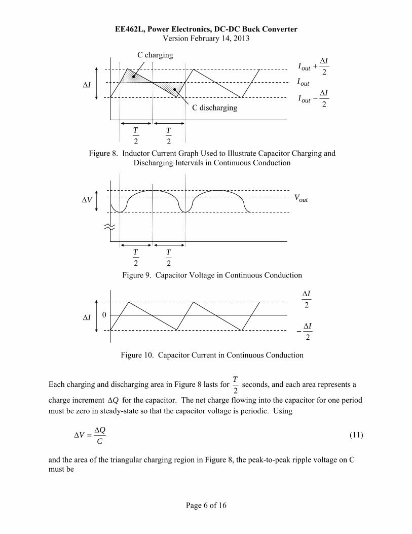
Page 6 of 16
Each charging and discharging area in Figure 8 lasts for 2
T seconds, and each area represents a
charge increment Q for the capacitor. The net charge flowing into the capacitor for one period must be zero in steady-state so that the capacitor voltage is periodic. Using
C
QV
(11)
and the area of the triangular charging region in Figure 8, the peak-to-peak ripple voltage on C must be
2
T
2
T
2
IIout
outI
2
IIout
Figure 8. Inductor Current Graph Used to Illustrate Capacitor Charging and Discharging Intervals in Continuous Conduction
I
C charging
C discharging
2
T
2
T
Figure 9. Capacitor Voltage in Continuous Conduction
V outV
2
I
2
I
Figure 10. Capacitor Current in Continuous Conduction
I 0

EE462L, Power Electronics, DC-DC Buck Converter Version February 14, 2013
Page 7 of 16
C
ITIT
CC
QV
8222
11
(12)
For the worst case, outII 2 , so
outIC
TV 2
8 . (13)
Thus, the worst case peak-to-peak voltage ripple on C is
Cf
IV out
4 . (14)
Component Ratings
Inductor and Capacitor Ratings – The inductor must have sufficient rms current rating for the current shown in Figure 4. The capacitor must support the maximum output voltage (i.e., corresponding to inV when D = 1) and the rms ripple current shown in Figure 10. The ripple
currents (i.e., total current minus average value) in Figures 4 and 10 are identical because of KCL at the node above C in Figure 1. A conservative estimate for rms inductor current is when
outII 2max , (15)
which when substituted into (8) yields
3
112
12
1 2222max, outoutoutLrms IIII , (16)
so that
outLrms II3
2max, . (17)
The same ripple current I also flows through C, but C has no average current. Using the same logic as in (15), the maximum squared rms current through C becomes
3
212
1
12
10
2222
max,out
outCrmsI
III , (18)
so that

EE462L, Power Electronics, DC-DC Buck Converter Version February 14, 2013
Page 8 of 16
3max,
outCrms
II . (19)
A conservative capacitor voltage rating is outV5.1 .
Diode Ratings – For the diode, a conservative voltage rating is inV2 because of the oscillatory
ringing transients that invariably occur with parasitic inductances and capacitances. To determine the current rating, examine the graph of diode current shown in Figure 11. A conservative assumption for diode current is to assume small D, so that the diode current is essentially the same as the inductor current. Thus, a conservative estimate is that diode rms current equals the inductor rms current given by (17). MOSFET Ratings – It is clear in Figure 1 that the MOSFET must conduct inductor current when closed, and hold off Vin when open. The actual voltage rating of the MOSFET should be at least twice Vin to allow for the oscillatory ringing transients that invariably occur. To determine the current rating, examine the graph of the MOSFET current shown in Figure 12.
DT (1–D)T
T
2maxI
ii LavgL
outLavg Ii
2minI
ii LavgL
Figure 11. Diode Current Waveform for Continuous Conduction
I
0
DT (1–D)T
T
2maxI
ii LavgL
outLavg Ii
2minI
ii LavgL
Figure 12. MOSFET Current for Continuous Conduction
I
0

EE462L, Power Electronics, DC-DC Buck Converter Version February 14, 2013
Page 9 of 16
A conservative assumption is to assume large D, so that the MOSFET current is essentially the same as the inductor current. Thus, a conservative estimate is that MOSFET rms current equals the inductor rms current given by (17). The Experiment Use #16 stranded wire for power wiring (red for +, black for –). 1. Using a 10” long piece of 1” by 6” wood, develop a plan for the layout of the circuit. This
board will contain only the buck converter. The MOSFET firing circuit will remain on its own wood piece.
2. Use the diode feature on your multimeter to identify the anode (P) and cathode (N) leads of
the diode. 3. Be sure to use a thin layer of heat sink compound when attaching the inductor and diode to
their heat sinks (see next step). 4. Complete the wiring of the circuit in Figure 1, using #16 stranded red and black wire for +
and – current carrying connections, respectively. Usually, a wide stripe down the side of a filter capacitor indicates the ground terminal. Secure the filter capacitor to a 1½” steel corner
Keep jumper connections short, ≈ 3 inches or less.
Mount 10µF ripple current capacitor across the input terminals

EE462L, Power Electronics, DC-DC Buck Converter Version February 14, 2013
Page 10 of 16
bracket with a nylon cable tie. Secure the inductor to its heat sink with a nylon screw and nut. Secure the diode and its heat sink to a 1½” steel corner bracket, using a #6-32 x ½” machine screw, flat washer, split washer, and nut. Be very careful with the diode polarity because, if it is connected backward, it will short circuit the input voltage. Likewise, the filter capacitor is an electrolytic, and it can rupture if connected backward. So be extra careful with capacitor polarity.
5. Mount a 10µF ripple current capacitor across the Vin terminals. (This capacitor will remain
in place when you modify your circuit later to become boost and buck/boost converters.) 6. Do not yet energize your circuit with a DBR. 7. Remove and discard the MOSFET snubber capacitor. 8. Connect a 12Vdc regulated “wall wart” to the DC jack of a MOSFET firing circuit. Observe
VGS on an oscilloscope while varying D and F over their ranges. VGS should have the desired rectangular appearance, and D and F should have the desired ranges.
9. Connect the MOSFET firing circuit to your buck converter, keeping the wires short (i.e, 3”
or less). Do not accidentally connect your buck converter to the MOSFET gate terminal. Then, after using an ohmmeter to make sure that none of the headlights are burned out, connect a 3-series headlight load to the output of your buck converter.
Important Note: the first time you energize your converter in Step 10, it is a good idea to feed the 120/25V transformer and DBR through a variac. That way, you can gradually increase the voltage and detect short circuits or other problems before they become serious. The ammeter on the variac is an excellent diagnostic tool. Once you are convinced that your circuit is working correctly, then you can remove the variac. 10. Connect a 25Vac transformer to a DBR. Connect the DBR to your buck converter, keeping
the wires short (i.e., 3” or less). Then, energize the 25Vac transformer and DBR. If using a
variac, adjust the variac so that Vac of the transformer is 27-28V.
11. Using the 3-headlight load, and with F = 50kHz, adjust D over the range 0.90 to 0.10, in
steps of 0.10, while recording Vin and Vout. Compare the Vout/Vin ratio to theory, and plot
the measured ratios and theoretical ratios versus D on one graph. For D = 0.90, obtain Iin
If your circuit has a short in Step 10, then do the following: 1. Make sure that your diode is not connected backwards. 2. Observe VGS on the MOSFET as you vary D and F. Does the waveform look correct?
3. Unplug the wall wart. Does the short circuit go away? If not, your MOSFET may be shorted – so, disconnect the MOSFET from the converter, and perform the voltage-controlled resistance test on the MOSFET.

EE462L, Power Electronics, DC-DC Buck Converter Version February 14, 2013
Page 11 of 16
and Iout by measuring the voltages across the bodies of the 0.01Ω resistors. Multiply to get
Pin and Pout, and then determine the efficiency of your buck converter. Check to see if your
MOSFET, diode, inductor, or output capacitor are “hot.” 12. Repeat the above step, using a 5Ω resistor as a load. 13. With 50kHz, D = 0.90, and the 5Ω load, use (5), (6), and (8) to compute inductor rms
current. Use (6) and (8), with avgI = 0, to compute capacitor rms current.
14. Keeping D = 0.90, lower F to its minimum (15-20kHz). Use your oscilloscope to measure
the peak-to-peak ripple voltage of Vin and Vout. Use “averaging with 1 cycle.”
Vin Ripple Voltage with 5Ω Load, D = 0.90, F = 15-20kHz
Vout Ripple Voltage with 5Ω Load, D = 0.90, F = 15-20kHz
Save screen snapshot #1
≈ 1.3Vpp
120Hz ripple in Vin
120Hz ripple in Vout

EE462L, Power Electronics, DC-DC Buck Converter Version February 14, 2013
Page 12 of 16
15. Approximating the Vout ripple waveform as a triangle wave, estimate its rms value using
12
22 pprms
VV ,
3212
pppprms
VVV . (for the example above, the result is VVrms 375.0 )
Compare the calculation result to that shown by a multimeter “AC” measurement.
16. Zoom-in the time scale to 20µsec/div and observe the 15-20kHz component of Vout. Freeze
the frame to take out the superimposed 120Hz background ripple. Compare the Vpp on the
scope to the “worst case” predicted by (14). Repeat the triangle-wave assumption Vrms
calculation. 17. While connected to Vout, use the FFT scope feature to determine the magnitude (in volts
rms) of the 120Hz and 15-20kHz components. Compare your rms readings to the triangle-wave assumption rms calculations of the previous two steps. How large is the 15-20kHz component compared to the 120Hz component?
≈ 0.1Vpp
15-20kHz Ripple Component of Vout

EE462L, Power Electronics, DC-DC Buck Converter Version February 14, 2013
Page 13 of 16
Spectral Content of Vout with 5Ω Load, D = 0.90, F = 15-20kHz
(Sample Rate, Span, and Center Frequency Shown)
Spectral Content of Vout with 5Ω Load, D = 0.90, F = 15-20kHz
(db Values of 120Hz and 16.5kHz Components Shown)
–34.38dB with respect to 1Vrms
Save screen snapshot #2
–9.06dB with respect to 1Vrms

EE462L, Power Electronics, DC-DC Buck Converter Version February 14, 2013
Page 14 of 16
18. Move the oscilloscope probe to view VDS. Measure the peak value of VDS for the
following two cases: A. without ripple current capacitor, and B. with ripple current capacitor.
Case A. VDS without Ripple Current Capacitor
Case B. Effect of Adding Ripple Current Capacitor
Save screen snapshot #3
EE462L, Power Electronics, DC-DC Buck Converter Version February 14, 2013
Page 15 of 16
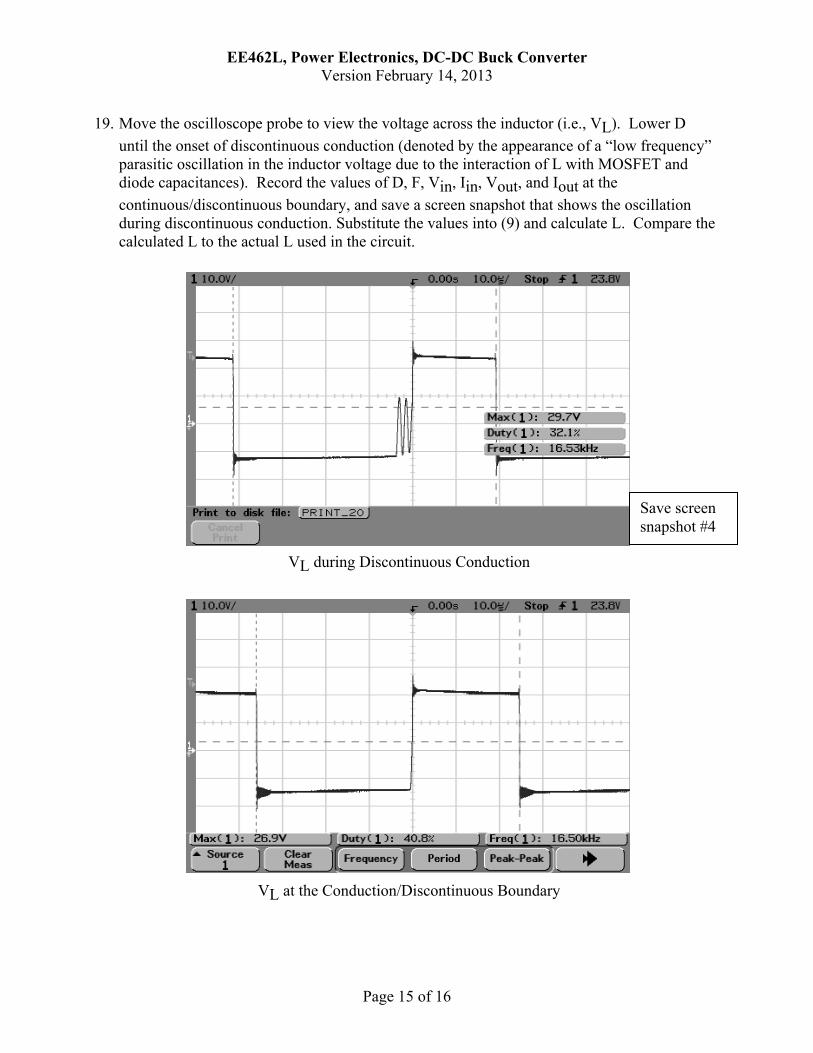
19. Move the oscilloscope probe to view the voltage across the inductor (i.e., VL). Lower D
until the onset of discontinuous conduction (denoted by the appearance of a “low frequency” parasitic oscillation in the inductor voltage due to the interaction of L with MOSFET and diode capacitances). Record the values of D, F, Vin, Iin, Vout, and Iout at the
continuous/discontinuous boundary, and save a screen snapshot that shows the oscillation during discontinuous conduction. Substitute the values into (9) and calculate L. Compare the calculated L to the actual L used in the circuit.
VL at the Conduction/Discontinuous Boundary
VL during Discontinuous Conduction
Save screen snapshot #4

EE462L, Power Electronics, DC-DC Buck Converter Version February 14, 2013
Page 16 of 16
Parts List 200V, 16A ultrafast rectifier (Fairchild Semiconductor FES16DT, Mouser #512-FES16DT). Heat sinks for diode and inductor, approx. 1.5” x 1.75” for TO-220 case style, 9.6°C/W
(Aavid Thermalloy, Mouser #532-507222B00) Output cap is 1500 – 2200µF, 200V – 250V, 5Arms ripple current, electrolytic. (Panasonic
#ECE-T2EP152EA, 1500µF, 250V, 5.66Arms ripple at 10kHz-50kHz, Digikey #P10048-ND). Be careful with polarity.
Inductor is 100µH, 9A (J. W. Miller RF Choke, Model 1130-101K-RC, Newark #63K3321 or Mouser #542-1130-101K-RC)
#4-40 x 1” flat slotted nylon screw and lock nut (Eagle Plastics, Mouser #561-J440-1 and #561-H440, respectively) for mounting the inductor
One 0.01Ω current sensing resistor (for measuring output current) (in student parts bin). 10µF high-frequency bipolar capacitor (50V, 10A peak-to-peak ripple current, Xicon #140-
BPHR50V10-RC, Mouser #140-BPHR50V10-RC). This capacitor is not polarized. Five two-terminal, 30A terminal blocks Steel corner brackets (1½” for filter capacitor, and 1½” for diode and its heat sink, holes not
enlarged). 8” nylon cable tie (Eagle Plastics #481-0115, Mouser # 481-0115) (in student parts bin) 1” by 6” wood, 10” long piece Extra parts
For the student parts bin and screw cabinet, at least 5 of the 250V MOSFETs (individually bagged) 5 of the 200V, 16A ultrafast rectifiers 5 of the DC jacks 5 of the 10kΩ audio taper and linear taper potentiometers 5 of the PWM modulator chips 5 of the inverting driver chips 5 of the 14-pin sockets 5 of the 8-pin DIP sockets 5 of the green plugs 10 of the #4-40 x 1” flat slotted nylon screws and lock nuts
Plastic bags for parts
6”x6”, 4mil for small parts 6”x8”, 6mil for holding everything