LM5146-Q1 100-V Synchronous Buck DC/DC Controller With ...
63
LM5146-Q1 100-V Synchronous Buck DC/DC Controller With Wide Duty Cycle Range 1 Features • AEC-Q100 qualified for automotive applications: – Device temperature grade 1: –40°C to +125°C ambient temperature range • Functional Safety-Capable – Documentation available to aid functional safety system design • Versatile synchronous buck DC/DC controller – Wide input voltage range of 5.5 V to 100 V – 150°C maximum junction temperature – 0.8-V reference with ±1% feedback accuracy – Adjustable output voltage from 0.8 V to 60 V – 40-ns t ON(min) for high V IN / V OUT ratio – 140-ns t OFF(min) for low dropout – Lossless R DS(on) or shunt current sensing – Optimized for CISPR 25 Class 5 requirements • Switching frequency from 100 kHz to 1 MHz – SYNC In and SYNC Out capability – Selectable diode emulation or FPWM • 7.5-V gate drivers for standard V TH MOSFETs – 14-ns adaptive dead-time control – 2.3-A source and 3.5-A sink capability • Inherent protection features for robust design – Adjustable output voltage soft start – Hiccup-mode overcurrent protection – Input UVLO with hysteresis – VCC and gate-drive UVLO protection – Precision enable input and open-drain PGOOD indicator for sequencing and control – Thermal shutdown protection with hysteresis • 20-pin VQFN package with wettable flanks • Create a custom design using the LM5146-Q1 with WEBENCH ® Power Designer 2 Applications • High-power automotive DC/DC regulator • Automotive motor drives, ADAS • HEV/EV powertrain systems • Body electronics and lighting • Infotainment and cluster 3 Description The LM5146-Q1 100-V synchronous buck controller regulates from a high input voltage source or from an input rail subject to high voltage transients, minimizing the need for external surge suppression components. A high-side switch minimum on-time of 40 ns gives large step-down ratios, enabling the direct step-down conversion from a 48-V nominal input to low-voltage rails for reduced system complexity and solution cost. The LM5146-Q1 continues to operate during input voltage dips as low as 5.5 V, at nearly 100% duty cycle if needed, making it an excellent choice for high- performance 48-V battery automotive applications, ADAS (surround view ECU) and HEV/EV systems. Forced-PWM (FPWM) operation eliminates switching frequency variation to minimize EMI, while user-selectable diode emulation lowers current consumption at light-load conditions. The adjustable switching frequency as high as 1 MHz can be synchronized to an external clock source to eliminate beat frequencies in noise-sensitive applications Device Information PART NUMBER PACKAGE (1) BODY SIZE (NOM) LM5146-Q1 VQFN (20) 4.50 mm × 3.50 mm (1) For all available packages, see the orderable addendum at the end of the data sheet. BST HO SW VCC PGND RT SS/TRK COMP FB AGND VIN VOUT LM5146-Q1 VOUT SYNC In GND PG SYNCOUT SYNCIN EN/UVLO VIN ILIM PGOOD SYNC Out LO LF COUT Q1 Q2 CIN RILIM CVCC CBST CSS RFB2 RFB1 RC2 CC2 CC1 RC1 CC3 RRT EN VIN Typical Application Circuit and Efficiency Performance, V OUT = 12 V, F SW = 400 kHz LM5146-Q1 SNVSB32B – AUGUST 2018 – REVISED JUNE 2021 An IMPORTANT NOTICE at the end of this data sheet addresses availability, warranty, changes, use in safety-critical applications, intellectual property matters and other important disclaimers. PRODUCTION DATA.
-
Upload
khangminh22 -
Category
Documents
-
view
5 -
download
0
Transcript of LM5146-Q1 100-V Synchronous Buck DC/DC Controller With ...

LM5146-Q1 100-V Synchronous Buck DC/DC Controller With Wide Duty Cycle Range
1 Features• AEC-Q100 qualified for automotive applications:
– Device temperature grade 1: –40°C to +125°Cambient temperature range
• Functional Safety-Capable– Documentation available to aid functional safety
system design• Versatile synchronous buck DC/DC controller
– Wide input voltage range of 5.5 V to 100 V– 150°C maximum junction temperature– 0.8-V reference with ±1% feedback accuracy– Adjustable output voltage from 0.8 V to 60 V– 40-ns tON(min) for high VIN / VOUT ratio– 140-ns tOFF(min) for low dropout– Lossless RDS(on) or shunt current sensing– Optimized for CISPR 25 Class 5 requirements
• Switching frequency from 100 kHz to 1 MHz– SYNC In and SYNC Out capability– Selectable diode emulation or FPWM
• 7.5-V gate drivers for standard VTH MOSFETs– 14-ns adaptive dead-time control– 2.3-A source and 3.5-A sink capability
• Inherent protection features for robust design– Adjustable output voltage soft start– Hiccup-mode overcurrent protection– Input UVLO with hysteresis– VCC and gate-drive UVLO protection– Precision enable input and open-drain PGOOD
indicator for sequencing and control– Thermal shutdown protection with hysteresis
• 20-pin VQFN package with wettable flanks• Create a custom design using the LM5146-Q1 with
WEBENCH® Power Designer
2 Applications• High-power automotive DC/DC regulator• Automotive motor drives, ADAS• HEV/EV powertrain systems• Body electronics and lighting• Infotainment and cluster
3 DescriptionThe LM5146-Q1 100-V synchronous buck controllerregulates from a high input voltage source or from aninput rail subject to high voltage transients, minimizingthe need for external surge suppression components.A high-side switch minimum on-time of 40 ns giveslarge step-down ratios, enabling the direct step-downconversion from a 48-V nominal input to low-voltagerails for reduced system complexity and solution cost.The LM5146-Q1 continues to operate during inputvoltage dips as low as 5.5 V, at nearly 100% dutycycle if needed, making it an excellent choice for high-performance 48-V battery automotive applications,ADAS (surround view ECU) and HEV/EV systems.
Forced-PWM (FPWM) operation eliminates switchingfrequency variation to minimize EMI, whileuser-selectable diode emulation lowers currentconsumption at light-load conditions. The adjustableswitching frequency as high as 1 MHz can besynchronized to an external clock source to eliminatebeat frequencies in noise-sensitive applications
Device InformationPART NUMBER PACKAGE(1) BODY SIZE (NOM)
LM5146-Q1 VQFN (20) 4.50 mm × 3.50 mm
(1) For all available packages, see the orderable addendum atthe end of the data sheet.
BST
HO
SW
VCC
PGND
RT
SS/TRK
COMP
FB
AGND
VIN
VOUT
LM5146-Q1
VOUT
SYNC In
GND
PG
SYNCOUT
SYNCIN
EN/UVLOVIN
ILIMPGOOD
SYNC Out
LO
LF
COUT
Q1
Q2
CIN
RILIM
CVCC
CBST
CSS
RFB2
RFB1
RC2
CC2
CC1
RC1
CC3
RRT
ENVIN
Typical Application Circuit and Efficiency Performance, VOUT = 12 V, FSW = 400 kHz
LM5146-Q1SNVSB32B – AUGUST 2018 – REVISED JUNE 2021
An IMPORTANT NOTICE at the end of this data sheet addresses availability, warranty, changes, use in safety-critical applications,intellectual property matters and other important disclaimers. PRODUCTION DATA.

Table of Contents1 Features............................................................................12 Applications .................................................................... 13 Description.......................................................................14 Revision History.............................................................. 25 Description (continued).................................................. 36 Pin Configuration and Functions...................................4
6.1 Wettable Flanks.......................................................... 57 Specifications.................................................................. 6
7.1 Absolute Maximum Ratings ....................................... 67.2 ESD Ratings ............................................................. 67.3 Recommended Operating Conditions ........................77.4 Thermal Information ...................................................77.5 Electrical Characteristics ............................................87.6 Switching Characteristics .........................................107.7 Typical Characteristics.............................................. 11
8 Detailed Description......................................................168.1 Overview................................................................... 168.2 Functional Block Diagram......................................... 168.3 Feature Description...................................................17
8.4 Device Functional Modes..........................................259 Application and Implementation.................................. 27
9.1 Application Information............................................. 279.2 Typical Applications.................................................. 36
10 Power Supply Recommendations..............................4611 Layout...........................................................................47
11.1 Layout Guidelines................................................... 4711.2 Layout Example...................................................... 50
12 Device and Documentation Support..........................5112.1 Device Support....................................................... 5112.2 Documentation Support.......................................... 5212.3 Receiving Notification of Documentation Updates..5212.4 Support Resources................................................. 5212.5 Trademarks.............................................................5312.6 Electrostatic Discharge Caution..............................5312.7 Glossary..................................................................53
13 Mechanical, Packaging, and OrderableInformation.................................................................... 54
4 Revision HistoryChanges from Revision A (November 2018) to Revision B (June 2021) Page• Updated the numbering format for tables, figures and cross-references throughout the document...................1• Added functional safety bullet.............................................................................................................................1• Updated Features .............................................................................................................................................. 1• Updated applications.......................................................................................................................................... 1• Changed min ILIM value to –1............................................................................................................................6• Corrected equation in Table 9-4 .......................................................................................................................31• Added conducted EMI plots..............................................................................................................................43• Updated Section 11.2 .......................................................................................................................................50• Added Table 12-1 in Section 12 .......................................................................................................................51• Updated Section 12.2 ...................................................................................................................................... 52
SPACER
Changes from Revision * (August 2018) to Revision A (November 2018) Page• First release of production-data data sheet........................................................................................................ 1
LM5146-Q1SNVSB32B – AUGUST 2018 – REVISED JUNE 2021 www.ti.com
2 Submit Document Feedback Copyright © 2021 Texas Instruments Incorporated
Product Folder Links: LM5146-Q1

5 Description (continued)Measuring the voltage drop across the low-side MOSFET or with an optional current sense resistor gives cycle-by-cycle overcurrent protection. The LM5146-Q1 voltage-mode controller with line feedforward drives externalhigh-side and low-side N-channel power switches with robust 7.5-V gate drivers suitable for standard-thresholdMOSFETs. Adaptively-timed gate drivers with 2.3-A source and 3.5-A sink capability minimize body diodeconduction during switching transitions, reducing switching losses and improving thermal performance whendriving MOSFETs at high input voltage and high frequency. The LM5146-Q1 can be powered from the output ofthe switching regulator or another available source, further improving efficiency.
A 180° out-of-phase clock output relative to the internal oscillator at SYNCOUT works well for cascaded ormulti-channel power supplies to reduce input capacitor ripple current and EMI filter size. Additional features ofthe LM5146-Q1 include a configurable soft start, an open-drain power-good monitor for fault reporting and outputmonitoring, monotonic start-up into prebiased loads, integrated VCC bias supply regulator and bootstrap diode,external power supply tracking, precision enable input with hysteresis for adjustable line undervoltage lockout(UVLO), hiccup-mode overload protection, and thermal shutdown protection with automatic recovery.
The LM5146-Q1 controller is offered in a 4.5-mm × 3.5-mm thermally enhanced, 20-pin VQFN package withadditional spacing for high-voltage pins and wettable flanks for optical inspection of solder joint fillets.
www.ti.comLM5146-Q1
SNVSB32B – AUGUST 2018 – REVISED JUNE 2021
Copyright © 2021 Texas Instruments Incorporated Submit Document Feedback 3
Product Folder Links: LM5146-Q1

6 Pin Configuration and Functions
VIN
RT
HO
SW
BST
LO
PGND
VCC
ILIM
SS/TRK
COMP
EN
/UV
LO
FB
AGND
PG
OO
D
SYNCOUT
SYNCIN
NC
EP
NC
2
3
4
5
6
7
8
9
10
19
18
17
16
15
14
13
12
Exposed
Pad
(EP)
1 20
11
Connect Exposed Pad on bottom to AGND and PGND on the PCB.
Figure 6-1. 20-Pin VQFN With Wettable Flanks in RGY Package (Top View)
Table 6-1. Pin FunctionsPIN
I/O(1) DESCRIPTIONNO. NAME
1 EN/UVLO I
Enable input and undervoltage lockout programming pin. If the EN/UVLO voltage is below 0.4 V, the controlleris in shutdown mode with all functions disabled. If the EN/UVLO voltage is greater than 0.4 V and less than1.2 V, the regulator is in standby mode with the VCC regulator operational, the SS pin grounded, and noswitching at the HO and LO outputs. If the EN/UVLO voltage is above 1.2 V, the SS/TRK voltage can rampand pulse-width modulated gate-drive signals are delivered to the HO and LO pins. A 10-μA current sourceis enabled when EN/UVLO exceeds 1.2 V and flows through the external UVLO resistor divider to providehysteresis. Hysteresis can be adjusted by varying the resistance of the external divider.
2 RT IOscillator frequency adjust pin. The internal oscillator is programmed with a single resistor between RT and theAGND. TI recommends a maximum oscillator frequency of 1 MHz. An RT pin resistor is required even whenusing the SYNCIN pin to synchronize to an external clock.
3 SS/TRK I
Soft start and voltage-tracking pin. An external capacitor and an internal 10-μA current source set the ramprate of the error amplifier reference during start-up. When the SS/TRK pin voltage is less than 0.8 V, theSS/TRK voltage controls the noninverting input of the error amp. When the SS/TRK voltage exceeds 0.8 V, theamplifier is controlled by the internal 0.8-V reference. SS/TRK is discharged to ground during standby and faultconditions. After start-up, the SS/TRK voltage is clamped 115 mV above the FB pin voltage. If FB falls due to aload fault, SS/TRK is discharged to a level 115 mV above FB to provide a controlled recovery when the fault isremoved. Voltage tracking can be implemented by connecting a low impedance reference between 0 V and 0.8V to the SS/TRK pin. The 10-µA SS/TRK charging current flows into the reference and produces a voltage errorif the impedance is not low. Connect a minimum capacitance from SS/TRK to AGND of 2.2 nF.
4 COMP O Low impedance output of the internal error amplifier. Connect the loop compensation network between theCOMP pin and the FB pin.
5 FB I Feedback connection to the inverting input of the internal error amplifier. A resistor divider from the output tothis pin sets the output voltage level. The regulation threshold at the FB pin is nominally 0.8 V.
6 AGND P Analog ground. Return for the internal 0.8-V voltage reference and analog circuits.
LM5146-Q1SNVSB32B – AUGUST 2018 – REVISED JUNE 2021 www.ti.com
4 Submit Document Feedback Copyright © 2021 Texas Instruments Incorporated
Product Folder Links: LM5146-Q1

Table 6-1. Pin Functions (continued)PIN
I/O(1) DESCRIPTIONNO. NAME
7 SYNCOUT O
Synchronization output. Logic output that provides a clock signal that is 180° out-of-phase with the high-sideFET gate drive. Connect SYNCOUT of the master LM5146-Q1 to the SYNCIN pin of a second LM5146-Q1 tooperate two controllers at the same frequency with 180° interleaved high-side FET switch turn-on transitions.Note that the SYNCOUT pin does not provide 180° interleaving when the controller is operating from anexternal clock that is different from the free-running frequency set by the RT resistor.
8 SYNCIN I
Dual function pin to provide an optional clock input and enable diode emulation by the low-side MOSFET.Connecting a clock signal to the SYNCIN pin synchronizes switching to the external clock. Diode emulationby the low-side MOSFET is disabled when the controller is synchronized to an external clock, and negativeinductor current can flow in the low-side MOSFET with light loads. A continuous logic low state at theSYNCIN pin enables diode emulation to prevent reverse current flow in the inductor. Diode emulation results indiscontinuous mode operation (DCM) at light loads, which improves efficiency. A logic high state at the SYNCINpin disables diode emulation, producing forced-PWM (FPWM) operation. During soft start when SYNCIN is highor a clock signal is present, the LM5146-Q1 operates in diode emulation mode until the output is in regulation,then gradually increases the SW zero-cross threshold, resulting in a gradual transition from DCM to FPWM.
9 NC — No electrical connection
10 PGOOD O Power-good indicator. This pin is an open-drain output. A high state indicates that the voltage at the FB pin iswithin a specified tolerance window centered at 0.8 V.
11 ILIM I
Current limit adjust and current sense comparator input. A current sourced from the ILIM pin through anexternal resistor programs the threshold voltage for valley current limiting. The opposite end of the thresholdadjust resistor can be connected to either the drain of the low-side MOSFET for RDS(on) sensing or to a currentsense resistor connected to the source of the low-side FET.
12 PGND P Power ground return pin for the low-side MOSFET gate driver. Connect directly to the source of the low-sideMOSFET or the ground side of a shunt resistor.
13 LO P Low-side MOSFET gate drive output. Connect to the gate of the low-side synchronous rectifier FET through ashort, low inductance path.
14 VCC O
Output of the 7.5-V bias regulator. Locally decouple to PGND using a low-ESR/ESL capacitor located as closeas possible to the controller. Controller bias can be supplied from an external supply that is greater than theinternal VCC regulation voltage. Use caution when applying external bias to ensure that the applied voltage isnot greater than the minimum VIN voltage and does not exceed the VCC pin maximum operating rating. See theRecommended Operating Conditions.
15 EP — Pin is internally connected to exposed pad of the package. Electrically isloated.
16 NC — No electrical connection
17 BST O
Bootstrap supply for the high-side gate driver. Connect to the bootstrap (boot) capacitor. The bootstrapcapacitor supplies current to the high-side FET gate and must be placed as close as possible to controller.If an external bootstrap diode is used to reduce the time required to charge the bootstrap capacitor, connect thecathode of the diode to the BST pin and anode to VCC.
18 HO P High-side MOSFET gate drive output. Connect to the gate of the high-side MOSFET through a short, lowinductance path.
19 SW P Switching node of the buck controller. Connect to the bootstrap capacitor, the source terminal of the high-sideMOSFET, and the drain terminal of the low-side MOSFET using short, low inductance paths.
20 VIN P Supply voltage input for the VCC LDO regulator
— EP — Exposed pad of the package. Electrically isolated. Solder to the system ground plane to reduce thermalresistance.
(1) P = Power, G = Ground, I = Input, O = Output
6.1 Wettable Flanks100% automated visual inspection (AVI) post-assembly is typically required to meet requirements for highreliability and robustness. Standard quad-flat no-lead (VQFN) packages do not have solderable or exposed pinsand terminals that are easily viewed. Therefore, it is difficult to visually determine whether or not the packageis successfully soldered onto the printed-circuit board (PCB). The wettable-flank process was developed toresolve the issue of side-lead wetting of leadless packaging. The LM5146-Q1 is assembled using a 20-pin VQFNpackage with wettable flanks to provide a visual indicator of solderability, which reduces the inspection time andmanufacturing costs.
www.ti.comLM5146-Q1
SNVSB32B – AUGUST 2018 – REVISED JUNE 2021
Copyright © 2021 Texas Instruments Incorporated Submit Document Feedback 5
Product Folder Links: LM5146-Q1

7 Specifications7.1 Absolute Maximum RatingsOver the recommended operating junction temperature of –40 to +150 (unless otherwise noted).(1)
MIN MAX UNIT
Input voltage
VIN –0.3 100
V
SW –1 100
SW (20-ns transient) –5 100
ILIM –1 100
EN/UVLO –0.3 100
VCC –0.3 14
FB, COMP, SS/TRK, RT –0.3 6
SYNCIN –0.3 14
Output voltage
BST –0.3 110
V
BST to VCC 100
BST to SW –0.3 14
VCC to BST (20-ns transient) 7
LO (20-ns transient) –3
PGOOD –0.3 14
Operating junction temperature, TJ 150 °C
Storage temperture, Tstg –55 150 °C
(1) Operation outside the Absolute Maximum Ratings may cause permanent device damage. Absolute Maximum Ratings do not implyfunctional operation of the device at these or any other conditions beyond those listed under Recommended Operating Conditions.If used outside the Recommended Operating Conditions but within the Absolute Maximum Ratings, the device may not be fullyfunctional, and this may affect device reliability, functionality, performance, and shorten the device lifetime.
7.2 ESD Ratings VALUE UNIT
V(ESD) Electrostatic discharge
Human body model (HBM), per AEC Q100-002 (1) HBM ESD Classification Level 2 ±2000
VCharged device model (CDM), per AEC Q100-011CDM ESD Classification Level C4B
All pins except 1, 2, 9, 10, 11, 12, and 20 ±500
Pins 1, 2, 9, 10, 11, 12, 19, and 20 ±750
(1) AEC Q100-002 indicates that HBM stressing shall be in accordance with the ANSI/ESDA/JEDEC JS-001 specification.
LM5146-Q1SNVSB32B – AUGUST 2018 – REVISED JUNE 2021 www.ti.com
6 Submit Document Feedback Copyright © 2021 Texas Instruments Incorporated
Product Folder Links: LM5146-Q1

7.3 Recommended Operating ConditionsOver the recommended operating junction temperature range of –40 to 150 (unless otherwise noted). (1)
MIN NOM MAX UNIT
Input voltage
VIN 5.5 100 V
SW –1 100 V
ILIM 0 100 V
External VCC bias rail 8 13 V
EN/UVLO –0.3 100 V
Outputvoltage
BST –0.3 110 V
BST to VCC 100 V
BST to SW 5 13 V
PGOOD 13 V
ISINK, ISRC Sink/source current SYNCOUT –1 1 mA
ISINK, ISRC Sink/source current PGOOD 2 mA
TJ Operating junction temperature –40 150 °C
(1) Recommended Operation Conditions are conditions under which the device is intended to be functional. For specifications and testconditions, see Electrical Characteristics.
7.4 Thermal Information
THERMAL METRIC(1)
LM5146-Q1
UNITRGY (VQFN)
20 PINS
RθJA Junction-to-ambient thermal resistance 36.8 °C/W
RθJC(top) Junction-to-case (top) thermal resistance 28 °C/W
RθJB Junction-to-board thermal resistance 11.8 °C/W
ψJT Junction-to-top characterization parameter 0.4 °C/W
ψJB Junction-to-board characterization parameter 11.7 °C/W
RθJC(bot) Junction-to-case (bottom) thermal resistance 2.1 °C/W
(1) For more information about traditional and new thermal metrics, see the Semiconductor and IC Package Thermal Metrics.
www.ti.comLM5146-Q1
SNVSB32B – AUGUST 2018 – REVISED JUNE 2021
Copyright © 2021 Texas Instruments Incorporated Submit Document Feedback 7
Product Folder Links: LM5146-Q1

7.5 Electrical CharacteristicsTypical values correspond to TJ = 25°C. Minimum and maximum limits apply over the –40°C to 150°C junction temperaturerange unless otherwise stated. VVIN = 48 V, VEN/UVLO = 1.5 V, RRT = 25 kΩ unless otherwise stated. (1) (2)
PARAMETER TEST CONDITIONS MIN TYP MAX UNITINPUT SUPPLYVIN Operating input voltage range IVCC ≤ 10 mA at VVIN = 5.5 V 5.5 100 V
IQ-RUN Operating input current, not switching VEN/UVLO = 1.5 V, VSS/TRK = 0 V 1.8 2.1 mA
IQ-STBY Standby input current VEN/UVLO = 1 V 1.75 2 mA
IQ-SHDN Shutdown input current VEN/UVLO = 0 V, VVCC < 1 V 13.5 30 µA
VCC REGULATOR
VVCC VCC regulation voltage VSS/TRK = 0 V, 9 V ≤ VVIN ≤ 100 V, 0mA ≤ IVCC ≤ 20 mA 7.3 7.5 7.7 V
VVCC-LDO VIN to VCC dropout voltage VVIN = 6 V, VSS/TRK = 0 V, IVCC = 20 mA 0.25 0.72 V
ISC-LDO VCC short-circuit current VSS/TRK = 0 V, VVCC = 0 V 40 50 70 mA
VVCC-UV VCC undervoltage threshold VVCC rising 4.8 4.93 5.2 V
VVCC-UVH VCC undervoltage hysteresis Rising threshold – falling threshold 0.26 V
VVCC-EXT Minimum external bias voltage Voltage required to disable VCCregulator 8 V
IVCCExternal VCC input current, notswitching VSS/TRK = 0 V, VVCC = 13 V 2.3 mA
ENABLE AND INPUT UVLOVSHDN Shutdown to standby threshold VEN/UVLO rising 0.42 V
VSHDN-HYS Shutdown threshold hysteresis EN/UVLO Rising threshold – fallingthreshold 50 mV
VEN Standby to operating threshold VEN/UVLO rising 1.164 1.2 1.236 V
IEN-HYS Standby to operating hysteresis current VEN/UVLO = 1.5 V 9 10 11 µA
ERROR AMPLIFIERVREF FB reference Voltage FB connected to COMP 792 800 808 mV
IFB-BIAS1 FB input bias current VFB = 0.8 V, –40°C ≤ TJ ≤ 125°C –0.1 0.1 µA
IFB-BIAS2 FB input bias current VFB = 0.8 V, –40 ≤ TJ ≤ 150 –0.2 0.2 µA
VCOMP-OH COMP output high voltage VFB = 0 V, COMP sourcing 1 mA 5 V
VCOMP-OL COMP output low voltage COMP sinking 1 mA 0.3 V
AVOL DC gain 94 dB
GBW Unity gain bandwidth 6.5 MHz
SOFT-START and VOLTAGE TRACKINGISS SS/TRK capacitor charging current VSS/TRK = 0 V 8.5 10 12 µA
RSS SS/TRK discharge FET resistance VEN/UVLO = 1 V, VSS/TRK = 0.1 V 11 Ω
VSS-FB SS/TRK to FB offset –15 0 15 mV
VSS-CLAMP SS/TRK clamp voltage VSS/TRK – VFB, VFB = 0.8 V 115 mV
POWER GOOD INDICATOR
PGUTHFB upper threshold for PGOOD high tolow % of VREF, VFB rising 106% 108% 110%
PGLTHFB lower threshold for PGOOD high tolow % of VREF, VFB falling 90% 92% 94%
PGHYS_U PGOOD upper theshold hysteresis % of VREF 3%
PGHYS_L PGOOD lower threshold hysteresis % of VREF 2%
TPG-RISE PGOOD rising filter FB to PGOOD rising edge 25% µs
TPG-FALL PGOOD falling filter FB to PGOOD falling edge 25% µs
VPG-OL PGOOD low state output voltage VFB = 0.9 V, IPGOOD = 2 mA 150 mV
LM5146-Q1SNVSB32B – AUGUST 2018 – REVISED JUNE 2021 www.ti.com
8 Submit Document Feedback Copyright © 2021 Texas Instruments Incorporated
Product Folder Links: LM5146-Q1

Typical values correspond to TJ = 25°C. Minimum and maximum limits apply over the –40°C to 150°C junction temperaturerange unless otherwise stated. VVIN = 48 V, VEN/UVLO = 1.5 V, RRT = 25 kΩ unless otherwise stated. (1) (2)
PARAMETER TEST CONDITIONS MIN TYP MAX UNITIPG-OH PGOOD high state leakage current VFB = 0.8 V, VPGOOD = 13 V 400 nA
OSCILLATORFSW1 Oscilator frequency – 1 RRT = 100 kΩ 100 kHz
FSW2 Oscillator frequency – 2 RRT = 25 kΩ 380 400 420 kHz
FSW3 Oscillator frequency – 3 RRT = 12.5 kΩ 780 kHz
SYNCHRONIZATION INPUT AND OUTPUTFSYNC SYNCIN external clock frequency range % of nominal frequency set by RRT –20% 50%
VSYNC-IH SYNCIN input logic high 2 V
VSYNC-IL SYNCIN input logic low 0.8 V
RSYNC-IN SYNCIN input resistance VSYNCIN = 3 V 20 kΩ
TSYNCI-PW SYNCIN input minimum pulsewidth Minimum high state or low stateduration 50 ns
VSYNCO-OH SYNCOUT high-state output voltage ISYNCOUT = –1 mA (sourcing current) 3 V
VSYNCO-OL SYNCOUT low-state output voltage ISYNCOUT = 1 mA (sinking current) 0.4 V
TSYNCOUTDelay from HO rising to SYNCOUTleading edge
VSYNCIN = 0 V, TS = 1/FSW, FSW set byRRT
TS/2 –140 ns
TSYNCINDelay from SYNCIN rising to HOleading edge 50% to 50% 150 ns
GATE DRIVERSRHO-UP HO high state resistance, HO to BST VBST – VSW = 7 V, IHO = –100 mA 1.5 Ω
RHO-DOWN HO low state resistance, HO to SW VBST – VSW = 7 V, IHO = 100 mA 0.9 Ω
RLO-UP LO high state resistance, LO to VCC VBST – VSW = 7 V, ILO = –100 mA 1.5 Ω
RLO-DOWN LO low state resistance, LO to PGND VBST – VSW = 7 V, ILO = 100 mA 0.9 Ω
IHOH, ILOH HO, LO source current VBST – VSW = 7 V, HO = SW, LO =AGND 2.3 A
IHOL, ILOL HO, LO sink current VBST – VSW = 7 V, HO = BST, LO = VCC 3.5 A
BOOTSTRAP DIODE AND UNDERVOLTAGE THRESHOLDVBST-FWD Diode forward voltage, VCC to BST VCC to BST, BST pin sourcing 20 mA 0.75 0.9 V
IQ-BSTBST to SW quiescent current, notswitching VSS/TRK = 0 V, VSW = 48 V, VBST = 54 V 80 µA
VBST-UV BST to SW undervoltage detection VBST – VSW falling 3.4 V
VBST-HYS BST to SW undervoltage hysteresis VBST – VSW rising 0.42 V
PWM CONTROLtON(min) Minimum controllable on-time VBST – VSW = 7 V, HO 50% to 50% 40 60 ns
tOFF(min) Minimum off-time VBST – VSW = 7 V, HO 50% to 50% 140 200 ns
DC100kHz Maximum duty cycleFSW = 100 kHz, 6 V ≤ VVIN ≤ 60 V 98 99 %
DC400kHz FSW = 400 kHz, 6 V ≤ VVIN ≤ 60 V 90 94 %
VRAMP(min)RAMP valley voltage (COMP at 0% dutycycle) 300 mV
kFF PWM feedforward gain (VIN / VRAMP) 6 V ≤ VVIN ≤ 100 V 15 V/V
OVER CURRENT PROTECT (OCP) – VALLEY CURRENT LIMITINGIRS ILIM source current, RSENSE mode Low voltage detected at ILIM 90 100 110 µA
IRDSON ILIM source current, RDS-ON mode SW voltage detected at ILIM, TJ = 25°C 180 200 220 µA
IRDSONTC ILIM current tempco RDS-ON mode 4500 ppm/°C
IRSTC ILIM current tempco RSENSE mode 0 ppm/°C
VILIM-TH ILIM comparator threshold at ILIM –8 –2 3.5 mV
SHORT CIRCUIT PROTECTION (SCP) – DUTY CYCLE CLAMP
www.ti.comLM5146-Q1
SNVSB32B – AUGUST 2018 – REVISED JUNE 2021
Copyright © 2021 Texas Instruments Incorporated Submit Document Feedback 9
Product Folder Links: LM5146-Q1

Typical values correspond to TJ = 25°C. Minimum and maximum limits apply over the –40°C to 150°C junction temperaturerange unless otherwise stated. VVIN = 48 V, VEN/UVLO = 1.5 V, RRT = 25 kΩ unless otherwise stated. (1) (2)
PARAMETER TEST CONDITIONS MIN TYP MAX UNIT
VCLAMP-OSClamp offset voltage – no currentlimiting COMP to duty cycle clamp voltage 0.2 +
VVIN/75 V
VCLAMP-MIN Minimum clamp voltage Clamp voltage with continuous currentlimit
0.3 +VVIN/150 V
HICCUP MODE FAULT PROTECTION
CHICC-DEL Hiccup mode activation delay Clock cycles with current limiting beforeoff-time activated 128 cycles
CHICCUP Hiccup mode off time after activation Clock cycles with no switching followedby SS/TRK release 8192 cycles
DIODE EMULATION / DCM OPERATION
VZCD-SS Zero-cross detect (ZCD) soft-start ramp ZCD threshold measured at SW pin 50cycles after first HO pulse 0 mV
VZCD-DIS Zero-cross detect disable threshold ZCD threshold measured at SW pin1000 cycles after first HO pulse 200 mV
VDEM-TH Diode emulation zero-cross threshold Measured at SW with VSW rising –5 0 5 mV
THERMAL SHUTDOWNTSD Thermal shutdown threshold TJ rising 175 °C
TSD-HYS Thermal shutdown hysteresis 20 °C
(1) All minimum and maximum limits are specified by correlating the electrical characteristics to process and temperature variations andapplied statistical process control.
(2) The junction temperature (TJ in ) is calculated from the ambient temperature (TA in ) and power dissipation (PD in Watts) asfollows: TJ = TA + (PD × RΘJA) where RΘJA (in /W) is the package thermal impedance provided in .
7.6 Switching CharacteristicsTypical values correspond to TJ = 25.
PARAMETER TEST CONDITIONS MIN TYP MAX UNITTHO-TR TLO-TR
HO, LO rise times VBST – VSW = 7 V, CLOAD = 1 nF, 20% to 80% 7 ns
THO -TF TLO-TF
HO, LO fall times VBST – VSW = 7 V, CLOAD = 1 nF, 80% to 20% 4 ns
THO-DT HO turn-on dead timne VBST – VSW = 7 V, LO off to HO on, 50% to50% 14 ns
TLO-DT LO turn-on dead timne VBST – VSW = 7 V, HO off to LO on, 50% to50% 14 ns
LM5146-Q1SNVSB32B – AUGUST 2018 – REVISED JUNE 2021 www.ti.com
10 Submit Document Feedback Copyright © 2021 Texas Instruments Incorporated
Product Folder Links: LM5146-Q1

7.7 Typical CharacteristicsVVIN = 48 V, RRT = 25 kΩ, SYNCIN tied to VCC, EN/UVLO tied to VIN (unless otherwise noted).
Output Current (A)
Eff
icie
ncy (
%)
0 2 4 6 8 10 1260
65
70
75
80
85
90
95
100
VIN = 12VVIN = 24VVIN = 36VVIN = 48VVIN = 60VVIN = 75V
VOUT = 5 V FSW = 300 kHzSee Figure 9-5 RRT = 33.2 kΩ
Figure 7-1. Efficiency vs Load, CCM
Output Current (A)
Eff
icie
ncy (
%)
0 2 4 6 870
75
80
85
90
95
100
VIN = 15VVIN = 24VVIN = 36VVIN = 48VVIN = 60VVIN = 75V
VOUT = 12 V FSW = 400 kHzSee Figure 9-16 RRT = 24.9 kΩ
Figure 7-2. Efficiency vs Load, CCM
Junction Temperature (°C)
Fe
edback V
oltage (
V)
-50 -25 0 25 50 75 100 125 1500.792
0.794
0.796
0.798
0.8
0.802
0.804
0.806
0.808
Figure 7-3. FB Voltage vs Junction TemperatureJunction Temperature (°C)
Min
On-T
ime,
Min
Off-T
ime (
ns)
-50 -25 0 25 50 75 100 125 1500
20
40
60
80
100
120
140
160
tOFF(min) tON(min)
Figure 7-4. tON(min) and tOFF(min) vs JunctionTemperature
Input Voltage (V)
VIN
Shutd
ow
n Q
uie
scent C
urr
ent
(PA
)
0 20 40 60 80 1000
10
20
30
4040°C 25°C 125°C 150°C
VSW = 0 V VEN/UVLO = 0 V
Figure 7-5. IQ-SHD vs Input Voltage
Input Voltage (V)
VIN
Sta
ndby Q
uie
scent
Curr
ent
(mA
)
0 20 40 60 80 1001.4
1.6
1.8
2
2.2
40°C 25°C 150°C
VSW = 0 V VEN/UVLO = 1 V
Figure 7-6. IQ-STANDBY vs Input Voltage
www.ti.comLM5146-Q1
SNVSB32B – AUGUST 2018 – REVISED JUNE 2021
Copyright © 2021 Texas Instruments Incorporated Submit Document Feedback 11
Product Folder Links: LM5146-Q1

Input Voltage (V)
VIN
Opera
ting Q
uie
scent
Curr
ent
(mA
)
0 20 40 60 80 1001.4
1.6
1.8
2
2.2
40°C 25°C 150°C
VSW = 0 V VEN/UVLO = VVIN VSS/TRK = 0 V
Figure 7-7. IQ-OPERATING (Nonswitching) vs InputVoltage
Input Voltage (V)
VIN
Opera
ting C
urr
ent S
witchin
g (
mA
)
0 20 40 60 80 1002.5
2.75
3
3.25
3.5
3.75
4
40°C 25°C 150°C
VSW = 0 V HO, LO Open
Figure 7-8. IQ-OPERATING (Switching) vs InputVoltage
Input Voltage (V)
VIN
Op
era
tin
g Q
uie
sce
nt C
urr
en
t (m
A)
0 20 40 60 80 1000
0.1
0.2
0.3
0.4
0.5
0.6
VCC = 8V
VSW = 0 V VVCC = VBST = VILIM VFB = 0 V
Figure 7-9. VIN Quiescent Current with ExternalVCC Applied
Junction Temperature (°C)
ILIM
Curr
ent
Sourc
e (P
A)
-50 -25 0 25 50 75 100 125 1500
50
100
150
200
250
300
350
RDS-ON ModeRSENSE Mode
Figure 7-10. ILIM Current Source vs JunctionTemperature
Junction Temperature (°C)
Deadtim
e (
ns)
-50 -25 0 25 50 75 100 125 1500
5
10
15
20
25
HO to LOLO to HO
VSW = 0 V
Figure 7-11. Deadtime vs Junction Temperature
Junction Temperature (°C)
VC
C U
VLO
Thre
shold
(V
)
-50 -25 0 25 50 75 100 125 1504.2
4.4
4.6
4.8
5
5.2
RisingFalling
Figure 7-12. VCC UVLO Thresholds vs JunctionTemperature
LM5146-Q1SNVSB32B – AUGUST 2018 – REVISED JUNE 2021 www.ti.com
12 Submit Document Feedback Copyright © 2021 Texas Instruments Incorporated
Product Folder Links: LM5146-Q1

Junction Temperature (°C)
BS
T U
VLO
Thre
shold
(V
)
-50 -25 0 25 50 75 100 125 1503
3.2
3.4
3.6
3.8
4
RisingFalling
Figure 7-13. BST UVLO Thresholds vs JunctionTemperature
Junction Temperature (°C)
PG
OO
D U
VP
Thre
shold
s (
V)
-50 -25 0 25 50 75 100 125 15088
90
92
94
96
98
RisingFalling
Figure 7-14. PGOOD UVP Thresholds vs JunctionTemperature
Junction Temperature (°C)
PG
OO
D O
VP
Thre
shold
s (
V)
-50 -25 0 25 50 75 100 125 150100
102
104
106
108
110
RisingFalling
Figure 7-15. PGOOD OVP Thresholds vs JunctionTemperature
Junction Temperature (°C)
EN
Thre
shold
(V
)
-50 -25 0 25 50 75 100 125 1501.05
1.1
1.15
1.2
1.25
1.3
Figure 7-16. EN/UVLO Threshold vs JunctionTemperature
Junction Temperature (°C)
EN
Sta
ndby T
hre
shold
(V
)
-50 -25 0 25 50 75 100 125 1500.25
0.3
0.35
0.4
0.45
0.5
RisingFalling
Figure 7-17. EN Standby Thresholds vs JunctionTemperature
RT Resistance (k:)
Sw
itch
ing
Fre
qu
en
cy (
kH
z)
0 10 20 30 40 50 60 70 80 90 1000
200
400
600
800
1000
VSW = 0 V
Figure 7-18. Oscillator Frequency vs RTResistance
www.ti.comLM5146-Q1
SNVSB32B – AUGUST 2018 – REVISED JUNE 2021
Copyright © 2021 Texas Instruments Incorporated Submit Document Feedback 13
Product Folder Links: LM5146-Q1

Junction Temperature (°C)
Sw
itchin
g F
requency (
kH
z)
-50 -25 0 25 50 75 100 125 150380
390
400
410
420
VIN = 6VVIN = 48VVIN = 100V
RRT = 25 kΩ
Figure 7-19. Oscillator Frequency vs JunctionTemperature
Junction Temperature (°C)
Sw
itch
ing
Fre
qu
en
cy (
kH
z)
-50 -25 0 25 50 75 100 125 150950
960
970
980
990
1000
VIN = 6VVIN = 48VVIN = 100V
RRT = 10 kΩ
Figure 7-20. Oscillator Frequency vs JunctionTemperature
VCC Voltage (V)
LO
, H
O G
ate
Dri
ve
r P
ea
k C
urr
en
t (A
)
6 7 8 9 10 11 12 131
1.5
2
2.5
3
3.5
4
SourceSink
Figure 7-21. Gate Driver Peak Current vs VCCVoltage
VCC Voltage (V)
HO
Ga
te D
rive
r R
DS
(on
) (:
)
6 7 8 9 10 11 12 130.6
0.8
1
1.2
1.4
1.6
High StateLow State
Figure 7-22. HO Driver Resistance vs VCC Voltage
VCC Voltage (V)
LO
Ga
te D
rive
r R
DS
(on
) (:
)
6 7 8 9 10 11 12 130.6
0.8
1
1.2
1.4
1.6
High StateLow State
Figure 7-23. LO Driver Resistance vs VCC Voltage
Input Voltage (V)
VC
C V
oltage (
V)
0 20 40 60 80 1005
5.5
6
6.5
7
7.5
8
40°C 25°C 150°C
VSS/TRK = 0 V
Figure 7-24. VCC Voltage vs Input Voltage
LM5146-Q1SNVSB32B – AUGUST 2018 – REVISED JUNE 2021 www.ti.com
14 Submit Document Feedback Copyright © 2021 Texas Instruments Incorporated
Product Folder Links: LM5146-Q1

VCC Current (mA)
VC
C V
oltage (
V)
0 10 20 30 40 50 600
1
2
3
4
5
6
740°C 25°C 125°C 150°C
VIN = 5.5 V
Figure 7-25. VCC vs ICC Characteristic
VCC Current (mA)
VC
C V
oltage (
V)
0 10 20 30 40 50 600
1
2
3
4
5
6
7
8
40°C 25°C 150°C
VIN = 12 V
Figure 7-26. VCC vs ICC Characteristic
BST Diode Forward Current (mA)
BS
T D
iod
e F
orw
ard
Vo
lta
ge
(V
)
0 10 20 30 40 500.5
0.6
0.7
0.8
0.9
1
VCC = 8V
Figure 7-27. BST Diode Forward Voltage vs CurrentJunction Temperature (°C)
Soft
-Sta
rt C
urr
ent (P
A)
-50 -25 0 25 50 75 100 125 1509.4
9.6
9.8
10
10.2
10.4
10.6
Figure 7-28. SS/TRK Current Source vs JunctionTemperature
www.ti.comLM5146-Q1
SNVSB32B – AUGUST 2018 – REVISED JUNE 2021
Copyright © 2021 Texas Instruments Incorporated Submit Document Feedback 15
Product Folder Links: LM5146-Q1

8 Detailed Description8.1 OverviewThe LM5146-Q1 is a 100-V synchronous buck controller with all of the functions necessary to implement a high-efficiency step-down power supply. The output voltage range is from 0.8 V to 60 V. The voltage-mode controlarchitecture uses input feedforward for excellent line transient response over a wide VIN range. Voltage-modecontrol supports the wide duty cycle range for high input voltage and low dropout applications as well as whena high-voltage conversion ratio (for example, 10-to-1) is required. Current sensing for cycle-by-cycle current limitcan be implemented with either the low-side FET RDS(on) or a current sense resistor. The operating frequencyis programmable from 100 kHz to 1 MHz. The LM5146-Q1 drives external high-side and low-side NMOS powerswitches with robust 7.5-V gate drivers suitable for standard threshold MOSFETs. Adaptive dead-time controlbetween the high-side and low-side drivers minimizes body diode conduction during switching transitions. Anexternal bias supply can be connected to the VCC pin to improve efficiency in high-voltage applications. Auser-selectable diode emulation feature enables DCM operation for improved efficiency and lower dissipation atlight-load conditions.
8.2 Functional Block Diagram
VIN VCC
BST
PGND
AGND
ILIM
SW
ERROR AMP
VCCUVLO
7.5 V LDO REGULATOR
HO
LO
RT
SS/TRK
COMP
PWMCOMPARATOR
0.8 V
THERMALSHUTDOWN
ENABLE LOGIC
OSCILLATOR & FEEDFORWARD
RAMPGENERATOR
EN/UVLO
0.4 V
HYSTERESIS
1.2 V STANDBY
SHUTDOWN
CLK
SYNCOUT
kFF*VIN
VCC ENABLE
PWMLOGIC
SYNCIN
SUPERVISORY COMPARATORS
PGOOD
0.8 V + 8%
FB
VCC
+
CURRENT LIMIT COMPARATOR
+
+±
+±
+± 7.5 V
FPWM
ILIM
LEVELSHIFT
ADAPTIVEDEADTIME
DELAY
+
COMPCLAMP
MODULATOR
LO
+
+ 0.8 V - 8%
25 µs delay
5 µsFILTER
STANDBY
PEAK DETECT FILTER
LOOCP
+
+
±
+115 mV
FB
RAMP
kFF*VIN + 0.3 V
0.3 V
BST_UV
VSW +VBST-UV
+
+
QCL
D R³1´
VVCC-UV
DRIVER
DRIVER
RDS(on) orShunt Sensing
HICCUP COUNTERS
CLK
±
±
±
±
±
±
±
±
±
+
CLAMP
ZERO CROSS DETECTION
LM5146-Q1SNVSB32B – AUGUST 2018 – REVISED JUNE 2021 www.ti.com
16 Submit Document Feedback Copyright © 2021 Texas Instruments Incorporated
Product Folder Links: LM5146-Q1

8.3 Feature Description8.3.1 Input Range (VIN)
The LM5146-Q1 operational input voltage range is from 5.5 V to 100 V. The device is intended for step-downconversions from 12-V, 24-V, 48-V, 60-V, and 72-V unregulated, semiregulated, and fully-regulated supply rails.The application circuit in Figure 8-1 shows all the necessary components to implement an LM5146-Q1-basedwide-VIN step-down regulator using a single supply. The LM5146-Q1 uses an internal LDO subregulator toprovide a 7.5-V VCC bias rail for the gate drive and control circuits (assuming the input voltage is higher than 7.5V plus the necessary subregulator dropout specification).
1
2
3
4
5
6
7
10 11
17
18
19
14
20
BST
HO
SW
LO
PGND
RT
SS/TRK
COMP
FB
AGND
VIN
VOUT
LM5146-Q1
VOUT
SYNCGND
PG
12
SYNCOUT
8 SYNCIN
9 NC
EN/UVLO VIN
ILIMPGOOD
SYNC
out
13
VCC
16
15
NC
EP
LF
COUT
Q1
Q2
CIN
RILIM
CVCC
CBST
CSS
RUV2 RUV1
RFB2
RFB1
RC2
CC2
CC1RC1
CC3
RPG
optional
RRT
Copyright © 2018, Texas Instruments Incorporated
CILIM
Figure 8-1. Schematic Diagram for VIN Operating Range of 5.5 V to 100 V
In high-voltage applications, take extra care to ensure the VIN pin does not exceed the absolute maximumvoltage rating of 100 V during line or load transient events. Voltage ringing on the VIN pin that exceeds thevalues in the Absolute Maximum Ratings can damage the IC. Use high-quality ceramic input capacitors tominimize ringing. An RC filter from the input rail to the VIN pin (for example, 4.7 Ω and 0.1 µF) providessupplementary filtering at the VIN pin.
8.3.2 Output Voltage Setpoint and Accuracy (FB)
The reference voltage at the FB pin is set at 0.8 V with a feedback system accuracy over the full junctiontemperature range of ±1%. Junction temperature range for the device is –40°C to +125°C. While dependent onswitching frequency and load current requirements, the LM5146-Q1 is generally capable of providing an outputvoltage in the range of 0.8 V to a maximum of slightly less than VIN. The DC output voltage setpoint duringnormal operation is set by the feedback resistor network, RFB1 and RFB2, connected to the output.
8.3.3 High-Voltage Bias Supply Regulator (VCC)
The LM5146-Q1 contains an internal high-voltage VCC regulator that provides a bias supply for the PWMcontroller and its gate drivers for the external MOSFETs. The input pin (VIN) can be connected directly to aninput voltage source up to 100 V. The output of the VCC regulator is set to 7.5 V. However, when the inputvoltage is below the VCC setpoint level, the VCC output tracks VIN with a small voltage drop. Connect a ceramicdecoupling capacitor between 1 µF and 5 µF from VCC to AGND for stability.
www.ti.comLM5146-Q1
SNVSB32B – AUGUST 2018 – REVISED JUNE 2021
Copyright © 2021 Texas Instruments Incorporated Submit Document Feedback 17
Product Folder Links: LM5146-Q1

The VCC regulator output has a current limit of 40 mA (minimum). At power up, the regulator sources currentinto the capacitor connected to the VCC pin. When the VCC voltage exceeds its rising UVLO threshold of 4.93V, the output is enabled (if EN/UVLO is above 1.2 V), and the soft-start sequence begins. The output remainsactive until the VCC voltage falls below its falling UVLO threshold of 4.67 V (typical) or if EN/UVLO goes to astandby or shutdown state.
Internal power dissipation of the VCC regulator can be minimized by connecting the output voltage or anauxiliary bias supply rail (up to 13 V) to VCC using a diode DVCC as shown in Figure 8-2. A diode in series withthe input prevents reverse current flow from VCC to VIN if the input voltage falls below the external VCC rail.
20 VCC
LM5146-Q1
14VIN VCC-EXT
Required if VIN < VCC(EXT)
6
Copyright © 2018, Texas Instruments Incorporated
CVIN
0.1 PF
DVIN
VIN
CVCC
2.2 PF
DVCC
8V to 13V
AGND
5.5V to 100V
Figure 8-2. VCC Bias Supply Connection From VOUT or Auxiliary Supply
Note that a finite bias supply regulator dropout voltage exists and is manifested to a larger extent when drivinghigh gate charge (QG) power MOSFETs at elevated switching frequencies. For example, at VVIN = 6 V, the VCCvoltage is 5.8 V with a DC operating current, IVCC, of 20 mA. Such a low gate drive voltage can be insufficientto fully enhance the power MOSFETs. At the very least, MOSFET on-state resistance, RDS(ON), can increase atsuch low gate drive voltage.
Here are the main considerations when operating at input voltages below 7.5 V:
• Increased MOSFET RDS(on) at lower VGS, leading to Increased conduction losses and reduced OCP setpoint• Increased switching losses given the slower switching times when operating at lower gate voltages• Restricted range of suitable power MOSFETs to choose from (MOSFETs with RDS(on) rated at VGS = 4.5 V
become mandatory)
8.3.4 Precision Enable (EN/UVLO)
The EN/UVLO input supports adjustable input undervoltage lockout (UVLO) with hysteresis programmed bythe resistor values for application specific power-up and power-down requirements. EN/UVLO connects to acomparator-based input referenced to a 1.2-V bandgap voltage. An external logic signal can be used to drive theEN/UVLO input to toggle the output ON and OFF and for system sequencing or protection. The simplest wayto enable the operation of the LM5146-Q1 is to connect EN/UVLO directly to VIN. This allows self start-up ofthe LM5146-Q1 when VCC is within its valid operating range. However, many applications benefit from using aresistor divider RUV1 and RUV2 as shown in Figure 8-3 to establish a precision UVLO level.
Use Equation 1 and Equation 2 to calculate the UVLO resistors given the required input turn-on and turn-offvoltages.
IN(on) IN(off)UV1
HYS
V VR
I
(1)
ENUV2 UV1
IN(on) EN
VR R
V V
(2)
LM5146-Q1SNVSB32B – AUGUST 2018 – REVISED JUNE 2021 www.ti.com
18 Submit Document Feedback Copyright © 2021 Texas Instruments Incorporated
Product Folder Links: LM5146-Q1

VIN
1.2V Enable
Comparator
RUV1
RUV2
LM5146-Q1
1
EN/UVLO
Remote
Shutdown
10 A
vcc
Copyright © 2018, Texas Instruments Incorporated
Figure 8-3. Programmable Input Voltage UVLO Turn-on and Turn-off
The LM5146-Q1 enters a low IQ shutdown mode when EN/UVLO is pulled below approximately 0.4 V. Theinternal LDO regulator powers off and the internal bias supply rail collapses, shutting down the bias currents ofthe LM5146-Q1. The LM5146-Q1 operates in standby mode when the EN/UVLO voltage is between the hardshutdown and precision enable (standby) thresholds.
8.3.5 Power Good Monitor (PGOOD)
The LM5146-Q1 provides a PGOOD flag pin to indicate when the output voltage is within a regulation window.Use the PGOOD signal as shown in Figure 8-4 for start-up sequencing of downstream converters, faultprotection, and output monitoring. PGOOD is an open-drain output that requires a pullup resistor to a DC supplynot greater than 13 V. The typical range of pullup resistance is 10 kΩ to 100 kΩ. If necessary, use a resistordivider to decrease the voltage from a higher voltage pullup rail.
5FB
LM5146-Q1
1 EN/UVLO
RUV1
499 k
VOUT(MASTER) = 5 V
RFB1
RFB2
20 k
3.83 k
0.8 V 5FB
LM5146-Q1
1
RPG
20 k
RFB3
RFB4
20 k
6.34 k
0.8 V
VOUT(SLAVE) = 3.3 V
VIN(on) = 15 VVIN(off) = 10 V
Regulator #1Start-up based on
Input Voltage UVLO
Regulator #2 Sequential Start-up based on PGOOD
PGOOD 10 PGOOD 10
RUV2
43.2 k
EN/UVLO
Copyright © 2018, Texas Instruments Incorporated
Figure 8-4. Master-Slave Sequencing Implementation Using PGOOD and EN/UVLO
When the FB voltage exceeds 94% of the internal reference VREF, the internal PGOOD switch turns off andPGOOD can be pulled high by the external pullup. If the FB voltage falls below 92% of VREF, the internalPGOOD switch turns on, and PGOOD is pulled low to indicate that the output voltage is out of regulation.Similarly, when the FB voltage exceeds 108% of VREF, the internal PGOOD switch turns on, pulling PGOOD low.If the FB voltage subsequently falls below 105% of VREF, the PGOOD switch is turned off and PGOOD is pulledhigh. PGOOD has a built-in deglitch delay of 25 µs.
8.3.6 Switching Frequency (RT, SYNCIN)
There are two options for setting the switching frequency, FSW, of the LM5146-Q1, thus providing a power supplydesigner with a level of flexibility when choosing external components for various applications. To adjust the
www.ti.comLM5146-Q1
SNVSB32B – AUGUST 2018 – REVISED JUNE 2021
Copyright © 2021 Texas Instruments Incorporated Submit Document Feedback 19
Product Folder Links: LM5146-Q1

frequency, use a resistor from the RT pin to AGND, or synchronize the LM5146-Q1 to an external clock signalthrough the SYNCIN pin.
8.3.6.1 Frequency Adjust
Adjust the LM5146-Q1 free-running switching frequency by using a resistor from the RT pin to AGND. Theswitching frequency range is from 100 kHz to 1 MHz. The frequency set resistance, RRT, is governed byEquation 3. E96 standard-value resistors for common switching frequencies are given in Table 8-1.
4
RT
SW
10R k
F kHz: ª º¬ ¼
ª º¬ ¼ (3)
Table 8-1. Frequency Set ResistorsSWITCHING FREQUENCY
(kHz)FREQUENCY SET RESISTANCE
(kΩ)100 100
200 49.9
250 40.2
300 33.2
400 24.9
500 20
750 13.3
1000 10
8.3.6.2 Clock Synchronization
Apply an external clock synchronization signal to the LM5146-Q1 to synchronize switching in both frequency andphase. Requirements for the external clock SYNC signal are:
• Clock frequency range: 100 kHz to 1 MHz• Clock frequency: –20% to +50% of the free-running frequency set by RRT• Clock maximum voltage amplitude: 13 V• Clock minimum pulse width: 50 ns
1 Ps/DIV
VSYNCIN
2 V/DIV
VSW 10 V/DIV
Figure 8-5. Typical 400-kHz SYNCIN and SW Voltage Waveforms
Figure 8-5 shows a clock signal at 400 kHz and the corresponding SW node waveform (VIN = 48 V, VOUT = 5 V,free-running frequency = 280 kHz). The SW voltage waveform is synchronized with respect to the rising edge ofSYNCIN. The rising edge of the SW voltage is phase delayed relative to SYNCIN by approximately 100 ns.
LM5146-Q1SNVSB32B – AUGUST 2018 – REVISED JUNE 2021 www.ti.com
20 Submit Document Feedback Copyright © 2021 Texas Instruments Incorporated
Product Folder Links: LM5146-Q1

8.3.7 Configurable Soft Start (SS/TRK)
After the EN/UVLO pin exceeds its rising threshold of 1.2 V, the LM5146-Q1 begins charging the output to theDC level dictated by the feedback resistor network. The LM5146-Q1 features an adjustable soft start (set by acapacitor from the SS/TRK pin to GND) that determines the charging time of the output. A 10-µA current sourcecharges this soft-start capacitor. Soft start limits inrush current as a result of high output capacitance to avoidan overcurrent condition. Stress on the input supply rail is also reduced. The soft-start time, tSS, for the outputvoltage to ramp to its nominal level is set by Equation 4.
SS REF
SS
SS
C Vt
I
(4)
where
• CSS is the soft-start capacitance• VREF is the 0.8-V reference• ISS is the 10-µA current sourced from the SS/TRK pin
More simply, calculate CSS using Equation 5.
SS SSC nF 12.5 t ms ª º ª º¬ ¼ ¬ ¼ (5)
The SS/TRK pin is internally clamped to VFB + 115 mV to allow a soft start recovery from an overload event.The clamp circuit requires a soft-start capacitance greater than 2 nF for stability and has a current limit ofapproximately 2 mA.
8.3.7.1 Tracking
The SS/TRK pin also doubles as a tracking pin when master-slave power-supply tracking is required. Thistracking is achieved by simply dividing down the output voltage of the master with a simple resistor network.Coincident, ratiometric, and offset tracking modes are possible.
If an external voltage source is connected to the SS/TRK pin, the external soft-start capability of the LM5146-Q1is effectively disabled. The regulated output voltage level is reached when the SS/TRK pin reaches the 0.8-Vreference voltage level. It is the responsibility of the system designer to determine if an external soft-startcapacitor is required to keep the device from entering current limit during a start-up event. Likewise, the systemdesigner must also be aware of how fast the input supply ramps if the tracking feature is enabled.
PGOOD
2V/DIV
VOUT 1V/DIV
SS/TRK
160mV/DIV
94% VOUT92% VOUT
10 ms/DIV
Figure 8-6. Typical Output Voltage Tracking and PGOOD Waveforms
Figure 8-6 shows a triangular voltage signal directly driving SS/TRK and the corresponding output voltagetracking response. Nominal output voltage here is 5 V, with oscilloscope channel scaling chosen such that the
www.ti.comLM5146-Q1
SNVSB32B – AUGUST 2018 – REVISED JUNE 2021
Copyright © 2021 Texas Instruments Incorporated Submit Document Feedback 21
Product Folder Links: LM5146-Q1

waveforms overlap during tracking. As expected, the PGOOD flag transitions at thresholds of 94% (rising) and92% (falling) of the nominal output voltage setpoint.
Two practical tracking configurations, ratiometric and coincident, are shown in Figure 8-7. The most commonapplication is coincident tracking, used in core versus I/O voltage tracking in DSP and FPGA implementations.Coincident tracking forces the master and slave channels to have the same output voltage ramp rate until theslave output reaches its regulated setpoint. Conversely, ratiometric tracking sets the output voltage of the slaveto a fraction of the output voltage of the master during start-up.
5FB
LM5146-Q1
3 SS/TRK
RTRK1
RTRK2
26.7 k
10 k
VOUTSLAVE1 = 1.8 V
RFB1
RFB2
12.5 k
10 k
0.8 V 5FB
LM5146-Q1
3 SS/TRK
RTRK3
RTRK4
20 k
RFB3
RFB4
10 k
20 k
0.8 V
VOUTSLAVE2 = 1.2 V
VOUTMASTER = 3.3 V
Slave Regulator #1
Ratiometric Tracking
Slave Regulator #2
Coincident Tracking
8
SYNCIN
SYNCOUT
from Master
CSS1
2.2 nF
CSS2
2.2 nF
8
SYNCIN
10 k
Copyright © 2018, Texas Instruments Incorporated
Figure 8-7. Tracking Implementation With Master, Ratiometric Slave, and Coincident Slave Rails
For coincident tracking, connect the SS/TRK input of the slave regulator to a resistor divider from the outputvoltage of the master that is the same as the divider used on the FB pin of the slave. In other words, simplyselect RTRK3 = RFB3 and RTRK4 = RFB4 as shown in Figure 8-7. As the master voltage rises, the slave voltagerises identically (aside from the 80-mV offset from SS/TRK to FB when VFB is below 0.8 V). Eventually, the slavevoltage reaches its regulation voltage, at which point the internal reference takes over the regulation while theSS/TRK input continues to 115 mV above FB, and no longer controls the output voltage.
In all cases, to ensure that the output voltage accuracy is not compromised by the SS/TRK voltage being tooclose to the 0.8-V reference voltage, the final value of the SS/TRK voltage of the slave should be at least 100mV above FB.
8.3.8 Voltage-Mode Control (COMP)
The LM5146-Q1 incorporates a voltage-mode control loop implementation with input voltage feedforward toeliminate the input voltage dependence of the PWM modulator gain. This configuration allows the controller tomaintain stability throughout the entire input voltage operating range and provides optimal response to inputvoltage transient disturbances. The constant gain provided by the controller greatly simplifies loop compensationdesign because the loop characteristics remain constant as the input voltage changes, unlike a buck converterwithout voltage feedforward. An increase in input voltage is matched by a concomitant increase in ramp voltageamplitude to maintain constant modulator gain. The input voltage feedforward gain, kFF, is 15, equivalent to theinput voltage divided by the ramp amplitude, VIN/VRAMP. See Section 9.1.3 for more detail.
8.3.9 Gate Drivers (LO, HO)
The LM5146-Q1 gate driver impedances are low enough to perform effectively in high output current applicationswhere large die-size or paralleled MOSFETs with correspondingly large gate charge, QG, are used. Measured atVVCC = 7.5 V, the low-side driver of the LM5146-Q1 has a low impedance pulldown path of 0.9 Ω to minimizethe effect of dv/dt induced turn-on, particularly with low gate-threshold voltage MOSFETs. Similarly, the high-side
LM5146-Q1SNVSB32B – AUGUST 2018 – REVISED JUNE 2021 www.ti.com
22 Submit Document Feedback Copyright © 2021 Texas Instruments Incorporated
Product Folder Links: LM5146-Q1

driver has 1.5-Ω and 0.9-Ω pullup and pulldown impedances, respectively, for faster switching transition times,lower switching loss, and greater efficiency.
The high-side gate driver works in conjunction with an integrated bootstrap diode and external bootstrapcapacitor, CBST. When the low-side MOSFET conducts, the SW voltage is approximately at 0 V and CBST ischarged from VCC through the integrated boot diode. Connect a 0.1-μF or larger ceramic capacitor close to theBST and SW pins.
Furthermore, there is a proprietary adaptive dead-time control on both switching edges to prevent shoot-throughand cross-conduction, minimize body diode conduction time, and reduce body diode reverse recovery losses.
8.3.10 Current Sensing and Overcurrent Protection (ILIM)
The LM5146-Q1 implements a lossless current sense scheme designed to limit the inductor current during anoverload or short-circuit condition. Figure 8-8 portrays the popular current sense method using the on-stateresistance of the low-side MOSFET. Meanwhile, Figure 8-9 shows an alternative implementation with currentshunt resistor, RS. The LM5146-Q1 senses the inductor current during the PWM off-time (when LO is high).
VIN
VOUT
GND
LF
RILIM
ILIM
COUT
Q2
Q1
SW
LO
HO
Figure 8-8. MOSFET RDS(on) Current Sensing
VIN
VOUT
GND
LF
COUT
Q2
Q1
SW
LO
HO
RILIM
ILIM
RS
Figure 8-9. Shunt Resistor Current Sensing
The ILIM pin of the LM5146-Q1 sources a reference current that flows in an external resistor, designated RILIM,to program of the current limit threshold. A current limit comparator on the ILIM pin prevents further SW pulses ifthe ILIM pin voltage goes below GND. Figure 8-10 shows the implementation.
Resistor RILIM is tied to SW to use the RDS(on) of the low-side MOSFET as a sensing element (termed RDS(on)mode). Alternatively, RILIM is tied to a shunt resistor connected at the source of the low-side MOSFET (termedRSENSE mode). The LM5146-Q1 detects the appropriate mode at start-up and sets the source current amplitudeand temperature coefficient (TC) accordingly.
The ILIM current with RDS-ON sensing is 200 µA at 27°C junction temperature and incorporates a TC of +4500ppm/°C to generally track the RDS(on) temperature variation of the low-side MOSFET. Conversely, the ILIMcurrent is a constant 100 µA in RSENSE mode. This controls the valley of the inductor current during a steady-state overload at the output. Depending on the chosen mode, select the resistance of RILIM using Equation 6.
OUT LDS(on)Q2 DS(on)
RDSON
ILIM
OUT LS
RS
I I 2R , R sensing
IR
I I 2R , shunt sensing
I
'°
° ®
'°°
¯ (6)
where
• ΔIL is the peak-to-peak inductor ripple current• RDS(on)Q2 is the on-state resistance of the low-side MOSFET
www.ti.comLM5146-Q1
SNVSB32B – AUGUST 2018 – REVISED JUNE 2021
Copyright © 2021 Texas Instruments Incorporated Submit Document Feedback 23
Product Folder Links: LM5146-Q1

• IRDSON is the ILIM pin current in RDS-ON mode• RS is the resistance of the current-sensing shunt element• IRS is the ILIM pin current in RSENSE mode
Given the large voltage swings of ILIM in RDS(on) sensing mode, a capacitor designated CILIM connected fromILIM to PGND is essential to the operation of the valley current limit circuit. Choose this capacitance such thatthe time constant RILIM· CILIM is approximately 6 ns.
GND
LF
COUT
Q1
Q2
S Q
QR
VIN
VOUTGate
Driver
RILIM
CILIM
S Q
QR
PWML
ValleyPWM
ILIM
comparator
PWM
Latch
COMP
Clamp
Modulator
300 mV
IRAMP
VRAMP
+
CLK
PWM Comp
VCLAMP
PWM Aux
+
+VREF
Error Amp
+
IRDSON(TJ)
PGND
ILIM
LO
HO
FB
COMP
+±
SW
Figure 8-10. OCP Setpoint Defined by Current Source IRDSON and Resistor RILIM in RDS-ON Mode
Note that current sensing with a shunt component is typically implemented at lower output current levelsto provide accurate overcurrent protection. Burdened by the unavoidable efficiency penalty, PCB layout, andadditional cost implications, this configuration is not usually implemented in high-current applications (exceptwhere OCP setpoint accuracy and stability over the operating temperature range are critical specifications).
LM5146-Q1SNVSB32B – AUGUST 2018 – REVISED JUNE 2021 www.ti.com
24 Submit Document Feedback Copyright © 2021 Texas Instruments Incorporated
Product Folder Links: LM5146-Q1
8.3.11 OCP Duty Cycle Limiter
CLK
COMP
300 mV
PWML
Short
Applied
RAMP
CLAMP
ILIM Threshold
ValleyPWM
PWML terminated by
VRAMP > VCOMP
PWML terminated by
VRAMP > VCLAMP
Many
cycles
Inductor Current
Figure 8-11. OCP Duty Cycle Limiting Waveforms
In addition to valley current limiting, the LM5146-Q1 uses a proprietary duty-cycle limiter circuit to reduce thePWM on-time during an overcurrent condition. As shown in Figure 8-10, an auxiliary PWM comparator alongwith a modulated CLAMP voltage limits how quickly the on-time increases in response to a large step in theCOMP voltage that typically occurs with a voltage-mode control loop architecture.
As depicted in Figure 8-11, the CLAMP voltage, VCLAMP, is normally regulated above the COMP voltage toprovide adequate headroom during a response to a load-on transient. If the COMP voltage rises quickly duringan overloaded or shorted output condition, the on-time pulse terminates, thereby limiting the on-time and peakinductor current. Moreover, the CLAMP voltage is reduced if additional valley current limit events occur, furtherreducing the average output current. If the overcurrent condition exists for 128 continuous clock cycles, a hiccupevent is triggered and SS is pulled low for 8192 clock cycles before a soft-start sequence is initiated.
8.4 Device Functional Modes8.4.1 Shutdown Mode
The EN/UVLO pin provides ON / OFF control for the LM5146-Q1. When the EN/UVLO voltage is below 0.37 V(typical), the device is in shutdown mode. Both the internal bias supply LDO and the switching regulator are off.The quiescent current in shutdown mode drops to 13.5 μA (typical) at VIN = 48 V. The LM5146-Q1 also includesundervoltage protection of the internal bias LDO. If the internal bias supply voltage is below its UVLO thresholdlevel, the switching regulator remains off.
8.4.2 Standby Mode
The internal bias supply LDO has a lower enable threshold than the switching regulator. When the EN/UVLOvoltage exceeds 0.42 V (typical) and is below the precision enable threshold (1.2 V typically), the internal LDO ison and regulating. Switching action and output voltage regulation are disabled in standby mode.
8.4.3 Active Mode
The LM5146-Q1 is in active mode when the VCC voltage is above its rising UVLO threshold of 5 V and theEN/UVLO voltage is above the precision EN threshold of 1.2 V. The simplest way to enable the LM5146-Q1 isto tie EN/UVLO to VIN. This allows self start-up of the LM5146-Q1 when the input voltage exceeds the VCCthreshold plus the LDO dropout voltage from VIN to VCC.
www.ti.comLM5146-Q1
SNVSB32B – AUGUST 2018 – REVISED JUNE 2021
Copyright © 2021 Texas Instruments Incorporated Submit Document Feedback 25
Product Folder Links: LM5146-Q1

8.4.4 Diode Emulation Mode
The LM5146-Q1 provides a diode emulation feature that can be enabled to prevent reverse (drain-to-source)current flow in the low-side MOSFET. When configured for diode emulation, the low-side MOSFET is switchedoff when reverse current flow is detected by sensing of the SW voltage using a zero-cross comparator. Thebenefit of this configuration is lower power loss at no-load and light-load conditions, the disadvantage beingslower light-load transient response.
The diode emulation feature is configured with the SYNCIN pin. To enable diode emulation and thus achievediscontinuous conduction mode (DCM) operation at light loads, connect the SYNCIN pin to AGND or leaveSYNCIN floating. If forced PWM (FPWM) continuous conduction mode (CCM) operation is desired, tie SYNCINto VCC either directly or using a pullup resistor. Note that diode emulation mode is automatically engaged toprevent reverse current flow during a prebias start-up. A gradual change from DCM to CCM operation providesmonotonic start-up performance.
8.4.5 Thermal Shutdown
The LM5146-Q1 includes an internal junction temperature monitor. If the temperature exceeds 175°C (typical),thermal shutdown occurs. When entering thermal shutdown, the device:1. Turns off the high-side and low-side MOSFETs.2. Pulls SS/TRK and PGOOD low.3. Turns off the VCC regulator.4. Initiates a soft-start sequence when the die temperature decreases by the thermal shutdown hysteresis of
20°C (typical).
This is a non-latching protection, and the device will cycle into and out of thermal shutdown if the fault persists.
LM5146-Q1SNVSB32B – AUGUST 2018 – REVISED JUNE 2021 www.ti.com
26 Submit Document Feedback Copyright © 2021 Texas Instruments Incorporated
Product Folder Links: LM5146-Q1

9 Application and ImplementationNote
Information in the following applications sections is not part of the TI component specification,and TI does not warrant its accuracy or completeness. TI’s customers are responsible fordetermining suitability of components for their purposes, as well as validating and testing their designimplementation to confirm system functionality.
9.1 Application Information9.1.1 Design and Implementation
To expedite the process of designing of a LM5146-Q1-based regulator for a given application, use the LM5146-Q1 Quickstart Calculator available as a free download, as well as numerous LM5146-Q1 reference designspopulated in TI Designs™ reference design library, or the designs provided in Section 9.2. The LM5146-Q1 isalso WEBENCH® Designer enabled.
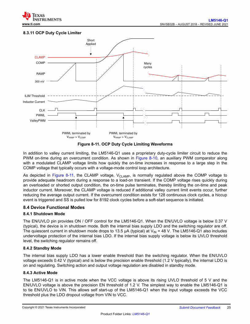
9.1.2 Power Train Components
Comprehensive knowledge and understanding of the power train components are key to successfully completinga synchronous buck regulator design.
9.1.2.1 Inductor
For most applications, choose an inductance such that the inductor ripple current, ΔIL, is between 30% and 40%of the maximum DC output current at nominal input voltage. Choose the inductance using Equation 7 based on apeak inductor current given by Equation 8.
OUT IN OUT
F
IN L SW
V V VL
V I F
§ · ¨ ¸
' © ¹ (7)
LL(peak) OUT
II I
2
'
(8)
Check the inductor data sheet to ensure that the saturation current of the inductor is well above the peakinductor current of a particular design. Ferrite designs have very low core loss and are preferred at highswitching frequencies, so design goals can then concentrate on copper loss and preventing saturation. Lowinductor core loss is evidenced by reduced no-load input current and higher light-load efficiency. However, ferritecore materials exhibit a hard saturation characteristic and the inductance collapses abruptly when the saturationcurrent is exceeded. This results in an abrupt increase in inductor ripple current, higher output voltage ripple,not to mention reduced efficiency and compromised reliability. Note that the saturation current of an inductorgenerally decreases as its core temperature increases. Of course, accurate overcurrent protection is key toavoiding inductor saturation.
9.1.2.2 Output Capacitors
Ordinarily, the output capacitor energy store of the regulator combined with the control loop response areprescribed to maintain the integrity of the output voltage within the dynamic (transient) tolerance specifications.The usual boundaries restricting the output capacitor in power management applications are driven by finiteavailable PCB area, component footprint and profile, and cost. The capacitor parasitics—equivalent seriesresistance (ESR) and equivalent series inductance (ESL)—take greater precedence in shaping the load transientresponse of the regulator as the load step amplitude and slew rate increase.
The output capacitor, COUT, filters the inductor ripple current and provides a reservoir of charge for step-loadtransient events. Typically, ceramic capacitors provide extremely low ESR to reduce the output voltage rippleand noise spikes, while tantalum and electrolytic capacitors provide a large bulk capacitance in a relativelycompact footprint for transient loading events.
www.ti.comLM5146-Q1
SNVSB32B – AUGUST 2018 – REVISED JUNE 2021
Copyright © 2021 Texas Instruments Incorporated Submit Document Feedback 27
Product Folder Links: LM5146-Q1

Based on the static specification of peak-to-peak output voltage ripple denoted by ΔVOUT, choose an outputcapacitance that is larger than that given by Equation 9.
L
OUT22
SW OUT ESR L
IC
8 F V R I
't
' ' (9)
Figure 9-1 conceptually illustrates the relevant current waveforms during both load step-up and step-downtransitions. As shown, the large-signal slew rate of the inductor current is limited as the inductor current rampsto match the new load-current level following a load transient. This slew-rate limiting exacerbates the deficitof charge in the output capacitor, which must be replenished as rapidly as possible during and after the loadstep-up transient. Similarly, during and after a load step-down transient, the slew rate limiting of the inductorcurrent adds to the surplus of charge in the output capacitor that must be depleted as quickly as possible.
load current,
iOUT(t)
IOUT1
IOUT2
'IOUT
tramp
IOUT2
IOUT1
'IOUT
inductor current, iL(t)
inductor current, iL(t)
load current, iOUT(t)
'QC
'QC
OUT OUT
ramp
di I
dt t
'
IN OUTL
F
V Vdi
dt L
OUTL
F
Vdi
dt L
Figure 9-1. Load Transient Response Representation Showing COUT Charge Surplus or Deficit
In a typical regulator application of 48-V input to low output voltage (for example, 5 V), the load-off transientrepresents the worst case in terms of output voltage transient deviation. In that conversion ratio application, thesteady-state duty cycle is approximately 10% and the large-signal inductor current slew rate when the duty cyclecollapses to zero is approximately –VOUT/L. Compared to a load-on transient, the inductor current takes muchlonger to transition to the required level. The surplus of charge in the output capacitor causes the output voltageto significantly overshoot. In fact, to deplete this excess charge from the output capacitor as quickly as possible,the inductor current must ramp below its nominal level following the load step. In this scenario, a large outputcapacitance can be advantageously employed to absorb the excess charge and limit the voltage overshoot.
To meet the dynamic specification of output voltage overshoot during such a load-off transient (denoted asΔVOVERSHOOT with step reduction in output current given by ΔIOUT), the output capacitance should be larger than
2
F OUT
OUT 2 2
OUT OVERSHOOT OUT
L IC
V V V
't
' (10)
The ESR of a capacitor is provided in the manufacturer’s data sheet either explicitly as a specification orimplicitly in the impedance vs. frequency curve. Depending on type, size and construction, electrolytic capacitorshave significant ESR, 5 mΩ and above, and relatively large ESL, 5 nH to 20 nH. PCB traces contribute someparasitic resistance and inductance as well. Ceramic output capacitors, on the other hand, have low ESR and
LM5146-Q1SNVSB32B – AUGUST 2018 – REVISED JUNE 2021 www.ti.com
28 Submit Document Feedback Copyright © 2021 Texas Instruments Incorporated
Product Folder Links: LM5146-Q1

ESL contributions at the switching frequency, and the capacitive impedance component dominates. However,depending on package and voltage rating of the ceramic capacitor, the effective capacitance can drop quitesignificantly with applied DC voltage and operating temperature.
Ignoring the ESR term in Equation 9 gives a quick estimation of the minimum ceramic capacitance necessaryto meet the output ripple specification. One to four 47-µF, 10-V, X7R capacitors in 1206 or 1210 footprint isa common choice. Use Equation 10 to determine if additional capacitance is necessary to meet the load-offtransient overshoot specification.
A composite implementation of ceramic and electrolytic capacitors highlights the rationale for parallelingcapacitors of dissimilar chemistries yet complementary performance. The frequency response of each capacitoris accretive in that each capacitor provides desirable performance over a certain portion of the frequency range.While the ceramic provides excellent mid- and high-frequency decoupling characteristics with its low ESR andESL to minimize the switching frequency output ripple, the electrolytic device with its large bulk capacitanceprovides low-frequency energy storage to cope with load transient demands.
9.1.2.3 Input Capacitors
Input capacitors are necessary to limit the input ripple voltage to the buck power stage due to switching-frequency AC currents. TI recommends using X5R or X7R dielectric ceramic capacitors to provide lowimpedance and high RMS current rating over a wide temperature range. To minimize the parasitic inductance inthe switching loop, position the input capacitors as close as possible to the drain of the high-side MOSFET andthe source of the low-side MOSFET. The input capacitor RMS current is given by Equation 11.
2
2 LCIN,rms OUT
II D I 1 D
12
§ ·'¨ ¸ ¨ ¸© ¹ (11)
The highest input capacitor RMS current occurs at D = 0.5, at which point the RMS current rating of thecapacitors should be greater than half the output current.
Ideally, the DC component of input current is provided by the input voltage source and the AC component by theinput filter capacitors. Neglecting inductor ripple current, the input capacitors source current of amplitude (IOUT −IIN) during the D interval and sinks IIN during the 1−D interval. Thus, the input capacitors conduct a square-wavecurrent of peak-to-peak amplitude equal to the output current. It follows that the resultant capacitive componentof AC ripple voltage is a triangular waveform. Together with the ESR-related ripple component, the peak-to-peakripple voltage amplitude is given by Equation 12.
OUT
IN OUT ESR
SW IN
I D 1 DV I R
F C
'
(12)
The input capacitance required for a particular load current, based on an input voltage ripple specification ofΔVIN, is given by Equation 13.
OUT
IN
SW IN ESR OUT
D 1 D IC
F V R I
t
' (13)
Low-ESR ceramic capacitors can be placed in parallel with higher valued bulk capacitance to provide optimizedinput filtering for the regulator and damping to mitigate the effects of input parasitic inductance resonating withhigh-Q ceramics. One bulk capacitor of sufficiently high current rating and two or three 2.2-μF 100-V X7Rceramic decoupling capacitors are usually sufficient. Select the input bulk capacitor based on its ripple currentrating and operating temperature.
9.1.2.4 Power MOSFETs
The choice of power MOSFETs has significant impact on DC/DC regulator performance. A MOSFET withlow on-state resistance, RDS(on), reduces conduction loss, whereas low parasitic capacitances enable faster
www.ti.comLM5146-Q1
SNVSB32B – AUGUST 2018 – REVISED JUNE 2021
Copyright © 2021 Texas Instruments Incorporated Submit Document Feedback 29
Product Folder Links: LM5146-Q1

transition times and reduced switching loss. Normally, the lower the RDS(on) of a MOSFET, the higher the gatecharge and output charge (QG and QOSS respectively), and vice versa. As a result, the product RDS(on) × QGis commonly specified as a MOSFET figure-of-merit. Low thermal resistance ensures that the MOSFET powerdissipation does not result in excessive MOSFET die temperature.
The main parameters affecting power MOSFET selection in a LM5146-Q1 application are as follows:
• RDS(on) at VGS = 7.5 V• Drain-source voltage rating, BVDSS, typically 60 V, 80 V, or 100 V, depending on maximum input voltage• Gate charge parameters at VGS = 7.5 V• Output charge, QOSS, at the relevant input voltage• Body diode reverse recovery charge, QRR• Gate threshold voltage, VGS(th), derived from the Miller plateau evident in the QG versus VGS plot in the
MOSFET data sheet. With a Miller plateau voltage typically in the range of 2 V to 5 V, the 7.5-V gate driveamplitude of the LM5146-Q1 provides an adequately-enhanced MOSFET when on and a margin againstCdv/dt shoot-through when off.
The MOSFET-related power losses are summarized by the equations presented in Table 9-1, where suffixes 1and 2 represent high-side and low-side MOSFET parameters, respectively. While the influence of inductor ripplecurrent is considered, second-order loss modes, such as those related to parasitic inductances and SW noderinging, are not included. Consult the LM5146-Q1 Quickstart Calculator to assist with power loss calculations.
Table 9-1. Buck Regulator MOSFET Power LossesPOWER LOSS MODE HIGH-SIDE MOSFET LOW-SIDE MOSFET
MOSFET conduction(2)(3)
22 L
cond1 OUT DS(on)1
IP D I R
12
§ ·'¨ ¸ ¨ ¸© ¹
22 L
cond2 OUT DS(on)2
IP D I R
12
§ ·'c ¨ ¸ ¨ ¸© ¹
MOSFET switchingª º ' '§ · § ·
« »¨ ¸ ¨ ¸© ¹ © ¹¬ ¼
IN SW L L
sw1 OUT R OUT F
V F I IP I t I t
2 2 2Negligible
MOSFET gate drive(1)Gate1 CC SW G1P V F Q Gate2 CC SW G2P V F Q
MOSFET outputcharge(4) Coss SW IN oss2 oss1 oss2P F V Q E E
Body diode conduction N/ABD
L L
cond F SW OUT dt1 OUT dt2
I IP V F I t I t
2 2
ª º' '§ · § · « »¨ ¸ ¨ ¸
© ¹ © ¹¬ ¼
Body diode reverserecovery(5) RR IN SW RR2P V F Q
(1) Gate drive loss is apportioned based on the internal gate resistance of the MOSFET, externally-added series gate resistance and therelevant gate driver resistance of the LM5146-Q1.
(2) MOSFET RDS(on) has a positive temperature coefficient of approximately 4500 ppm/°C. The MOSFET junction temperature, TJ, and itsrise over ambient temperature is dependent upon the device total power dissipation and its thermal impedance. When operating at ornear minimum input voltage, ensure that the MOSFET RDS(on) is rated at VGS = 4.5 V.
(3) D' = 1–D is the duty cycle complement.(4) MOSFET output capacitances, Coss1 and Coss2, are highly non-linear with voltage. These capacitances are charged losslessly by the
inductor current at high-side MOSFET turn-off. During turn-on, however, a current flows from the input to charge Coss2 of the low-sideMOSFET. Eoss1, the energy of Coss1, is dissipated at turnon, but this is offset by the stored energy Eoss2 on Coss2.
(5) MOSFET body diode reverse recovery charge, QRR, depends on many parameters, particularly forward current, current transitionspeed, and temperature.
The high-side (control) MOSFET carries the inductor current during the PWM on-time (or D interval) and typicallyincurs most of the switching losses. It is therefore imperative to choose a high-side MOSFET that balancesconduction and switching loss contributions. The total power dissipation in the high-side MOSFET is the sum ofthe losses due to conduction, switching (voltage-current overlap), output charge, and typically two-thirds of thenet loss attributed to body diode reverse recovery.
The low-side (synchronous) MOSFET carries the inductor current when the high-side MOSFET is off (or 1–Dinterval). The low-side MOSFET switching loss is negligible as it is switched at zero voltage – current justcommutates from the channel to the body diode or vice versa during the transition deadtimes. The LM5146-Q1,
LM5146-Q1SNVSB32B – AUGUST 2018 – REVISED JUNE 2021 www.ti.com
30 Submit Document Feedback Copyright © 2021 Texas Instruments Incorporated
Product Folder Links: LM5146-Q1
with its adaptive gate drive timing, minimizes body diode conduction losses when both MOSFETs are off. Suchlosses scale directly with switching frequency.
In high step-down ratio applications, the low-side MOSFET carries the current for a large portion of the switchingperiod. Therefore, to attain high efficiency, it is critical to optimize the low-side MOSFET for low RDS(on). In caseswhere the conduction loss is too high or the target RDS(on) is lower than available in a single MOSFET, connecttwo low-side MOSFETs in parallel. The total power dissipation of the low-side MOSFET is the sum of the lossesdue to channel conduction, body diode conduction, and typically one-third of the net loss attributed to body diodereverse recovery. The LM5146-Q1 is well suited to drive TI's portfolio of NexFET™ power MOSFETs.
9.1.3 Control Loop Compensation
The poles and zeros inherent to the power stage and compensator are respectively illustrated by red and bluedashed rings in the schematic embedded in Table 9-2. The compensation network typically employed withvoltage-mode control is a Type-III circuit with three poles and two zeros. One compensator pole is located atthe origin to realize high DC gain. The normal compensation strategy uses two compensator zeros to counteractthe LC double pole, one compensator pole located to nullify the output capacitor ESR zero, with the remainingcompensator pole located at one-half switching frequency to attenuate high frequency noise. The resistor dividernetwork to FB determines the desired output voltage. Note that the lower feedback resistor, RFB2, has noimpact on the control loop from an AC standpoint because the FB node is the input to an error amplifier and iseffectively at AC ground. Hence, the control loop is designed irrespective of output voltage level. The provisohere is the necessary output capacitance derating with bias voltage and temperature.
Table 9-2. Buck Regulator Poles and Zeros
FBCOMP
VIN
VOUT
GND
Adaptive
Gate
Driver
RFB2
RC2CC3
CC2
RFB1
RC1CC1
VREF
LF
D
PWM
Comparator
PWM Ramp
&p1
&z1
RESR
&p2
&z2
&o
&ESR
Modulator
Compensator
Power Stage
RL
IOUT
++
VRAMP
Error
Amp
&L
RDAMP
COUT
Q2
Q1
POWER STAGE POLES POWER STAGE ZEROS COMPENSATOR POLES COMPENSATOR ZEROS
o
ESR LF OUT
ESR DAMP
F OUT
1
1 R RL C
1 R R
1
L C
Z § ·
¨ ¸© ¹
#
(1) (2)
ESR
ESR OUT
1
R CZ
p1
C1 C1 C2 C1 C2
1 1
R (C C ) R CZ #
z1
C1 C1
1
R CZ
F
L
DAMP
L
RZ p2
C2 C3
1
R CZ
z2
FB1 C2 C3
1
(R R ) CZ
(1) RESR represents the ESR of the output capacitor COUT.(2) RDAMP = D · RDS(on)high-side + (1–D) · RDS(on) low-side + RDCR, shown as a lumped element in the schematic, represents the effective
series damping resistance.
The small-signal open-loop response of a buck regulator is the product of modulator, power train andcompensator transfer functions. The power stage transfer function can be represented as a complex pole pair
www.ti.comLM5146-Q1
SNVSB32B – AUGUST 2018 – REVISED JUNE 2021
Copyright © 2021 Texas Instruments Incorporated Submit Document Feedback 31
Product Folder Links: LM5146-Q1

associated with the output LC filter and a zero related to the ESR of the output capacitor. The DC (and lowfrequency) gain of the modulator and power stage is VIN/VRAMP. The gain from COMP to the average voltage atthe input of the LC filter is held essentially constant by the PWM line feedforward feature of the LM5146-Q1 (15V/V or 23.5 dB).
Complete expressions for small-signal frequency analysis are presented in Table 9-3. The transfer functions aredenoted in normalized form. While the loop gain is of primary importance, a regulator is not specified directlyby its loop gain but by its performance related characteristics, namely closed-loop output impedance and audiosusceptibility.
Table 9-3. Buck Regulator Small-Signal AnalysisTRANSFER FUNCTION EXPRESSION
Open-loop transfer functioncomp o
v c vd Mo comp
ÖÖv (s) Öv (s) d(s)T (s) G (s) G (s) F
ÖÖ Öv (s) v (s)d(s)
Duty-cycle-to-output transfer functionin
o
ovd IN 2
Öv (s) 0Öi (s) 0 2
s1
Öv (s)G (s) V
Öd(s) s s1
Z
Z Z
ESR
o o oQ
Compensator transfer function(1)
1
comp z2c mid
o
p1 p2
s1 1
Öv (s) sG (s) K
Öv (s) s s1 1
Z
Z
Z Z
§ ·§ · ¨ ¸¨ ¸
© ¹© ¹ § ·§ · ¨ ¸¨ ¸
¨ ¸¨ ¸© ¹© ¹
z
Modulator transfer function Mcomp RAMP
Öd(s) 1F
Öv (s) V
(1) Kmid = RC1/RFB1 is the mid-band gain of the compensator. By expressing one of the compensator zeros in inverted zero format, themid-band gain is denoted explicitly.
Figure 9-2 shows the open-loop response gain and phase. The poles and zeros of the system are marked withx and o symbols, respectively, and a + symbol indicates the crossover frequency. When plotted on a log (dB)scale, the open-loop gain is effectively the sum of the individual gain components from the modulator, powerstage, and compensator (see Figure 9-3). The open-loop response of the system is measured experimentally bybreaking the loop, injecting a variable-frequency oscillator signal, and recording the ensuing frequency responseusing a network analyzer setup.
-40
-20
0
20
40
-180
-135
-90
-45
0
1 10 100 1000
Frequency (kHz)
Loop
Gain
(dB)
Loop
Phase
(°)
Complex
LC Double
Pole
Compensator
Poles
Output
Capacitor
ESR Zero
Crossover
Frequency, fc
Compensator
Zeros
Loop
Phase
Loop
Gain
NM
Figure 9-2. Typical Buck Regulator Loop Gain and Phase With Voltage-Mode Control
LM5146-Q1SNVSB32B – AUGUST 2018 – REVISED JUNE 2021 www.ti.com
32 Submit Document Feedback Copyright © 2021 Texas Instruments Incorporated
Product Folder Links: LM5146-Q1

If the pole located at ωp1 cancels the zero located at ωESR and the pole at ωp2 is located well above crossover,the expression for the loop gain, Tv(s) in Table 9-3, can be manipulated to yield the simplified expression given inEquation 14.
2IN
v C1 C3RAMP
VT (s) R C
V s
Z
o
(14)
Essentially, a multi-order system is reduced to a single-order approximation by judicious choice of compensatorcomponents. A simple solution for the crossover frequency (denoted as fc in Figure 9-2) with Type-III voltage-mode compensation is derived as shown in Equation 15 and Equation 16.
IN
c o mid
RAMP
V2 f K
VZ S Z
c
(15)
c C1
mid
o FF FB1
f R1K
f k R
(16)
-40
-20
0
20
40
1 10 100 1000
Frequency (kHz)
Gain
(dB)
fc
Loop Gain
Filter Gain
Modulator
GainCompensator
Gain
Figure 9-3. Buck Regulator Constituent Gain Components
The loop crossover frequency is usually selected between one-tenth to one-fifth of switching frequency. Insertingan appropriate crossover frequency into Equation 16 gives a target for the mid-band gain of the compensator,Kmid. Given an initial value for RFB1, RFB2 is then selected based on the desired output voltage. Values for RC1,RC2, CC1, CC2, and CC3 are calculated from the design expressions listed in Table 9-4, with the premise that thecompensator poles and zeros are set as follows: ωz1 = 0.5·ωo, ωz2 = ωo, ωp1 = ωESD, and ωp2 = ωSW / 2.
Table 9-4. Compensation Component SelectionRESISTORS CAPACITORS
FB1
FB2
OUT REF
RR
V V 1
Z
C1
z1 C1
1C
R
C1 mid FB1R K R
Z
C2
p1 C1
1C
R
Z
C2
p2 C3
1R
C
1
C3
z2 FB1
CRZ
www.ti.comLM5146-Q1
SNVSB32B – AUGUST 2018 – REVISED JUNE 2021
Copyright © 2021 Texas Instruments Incorporated Submit Document Feedback 33
Product Folder Links: LM5146-Q1

Referring to the bode plot in Figure 9-2, the phase margin, indicated as φM, is the difference between the loopphase and –180° at crossover. A target of 50° to 70° for this parameter is considered ideal. Additional phaseboost is dialed in by locating the compensator zeros at a frequency lower than the LC double pole. This helpsmitigate the phase dip associated with the LC filter, particularly at light loads when the Q-factor is higher andthe phase dip becomes especially prominent. The ramification of low phase in the frequency domain is anunder-damped transient response in the time domain.
The power supply designer now has all the necessary expressions to optimally position the loop crossoverfrequency while maintaining adequate phase margin over the required line, load and temperature operatingranges. The LM5146-Q1 Quickstart Calculator is available to expedite these calculations and to adjust the bodeplot as needed.
9.1.4 EMI Filter Design
Switching regulators exhibit negative input impedance, which is lowest at the minimum input voltage. Anunderdamped LC filter exhibits a high output impedance at the resonant frequency of the filter. For stability,the filter output impedance must be less than the absolute value of the converter input impedance.
2IN(min)
ININ
VZ
P
(17)
The EMI filter design steps are as follows:
• Calculate the required attenuation of the EMI filter at the switching frequency, where CIN represents theexisting capacitance at the input of the switching converter.
• Input filter inductor LIN is usually selected between 1 μH and 10 μH, but it can be lower to reduce losses in ahigh current design.
• Calculate input filter capacitor CF full stop.
VIN
GND
LIN
CINCF
CD
RD
VOUT
LF
COUT
Q1
Q2
GND
Figure 9-4. Buck Regulator With π-Stage EMI Filter
By calculating the first harmonic current from the Fourier series of the input current waveform and multiplying itby the input impedance (the impedance is defined by the existing input capacitor CIN), a formula is derived toobtain the required attenuation as shown by Equation 18.
SS
§ ·¨ ¸ ¨ ¸ © ¹
L(PEAK)MAX MAX2
SW IN
I 1Attn 20log sin D V
19F C(18)
where
• VMAX is the noise specification in dBμV from the applicable EMI standard, for example CISPR 25 Class 5• CIN is the existing input capacitance of the buck regulator
LM5146-Q1SNVSB32B – AUGUST 2018 – REVISED JUNE 2021 www.ti.com
34 Submit Document Feedback Copyright © 2021 Texas Instruments Incorporated
Product Folder Links: LM5146-Q1

• DMAX is the maximum duty cycle• IPEAK is the peak inductor current
For filter design purposes, the current at the input can be modeled as a square-wave. Determine the EMI filtercapacitance CF from Equation 19.
2Attn
40
F
IN SW
1 10C
L 2 FS
§ ·¨ ¸¨ ¸
¨ ¸¨ ¸© ¹ (19)
Adding an input filter to a switching regulator modifies the control-to-output transfer function. The outputimpedance of the filter must be sufficiently small such that the input filter does not significantly affect the loopgain of the buck converter. The impedance peaks at the filter resonant frequency. The resonant frequency of thefilter is given by Equation 20.
res
IN F
1f
2 L CS
(20)
The purpose of RD is to reduce the peak output impedance of the filter at the resonant frequency. Capacitor CDblocks the DC component of the input voltage to avoid excessive power dissipation in RD. Capacitor CD musthave lower impedance than RD at the resonant frequency with a capacitance value greater than that of the inputcapacitor CIN. This prevents CIN from interfering with the cutoff frequency of the main filter. Added damping isneeded when the output impedance of the filter is high at the resonant frequency (Q of filter formed by LIN andCIN is too high). An electrolytic capacitor CD can be used for damping with a value given by Equation 21.
D INC 4 Ct (21)
Select the damping resistor RD using Equation 22.
IN
D
IN
LR
C
(22)
www.ti.comLM5146-Q1
SNVSB32B – AUGUST 2018 – REVISED JUNE 2021
Copyright © 2021 Texas Instruments Incorporated Submit Document Feedback 35
Product Folder Links: LM5146-Q1

9.2 Typical ApplicationsFor step-by-step design procedure, circuit schematics, bill of materials, PCB files, simulation and test results ofan LM5146-Q1-powered implementation, see TI Designs reference design library.9.2.1 Design 1 – 12-A High-Efficiency Synchronous Buck DC/DC Regulator for Automotive Applications
Figure 9-5 shows the schematic diagram of a 5-V, 12-A buck regulator with a switching frequency of 300 kHz.In this example, the target efficiencies are 94% and 92% at input voltages of 24 V and 48 V, respectively. Theinput UVLO is set to turn on and off at 8 V and 7 V, respectively. The switching frequency is set by meansof a synchronization input signal at 300 kHz, and the free-running switching frequency (in the event that thesynchronization signal is removed) is set at 250 kHz by resistor RRT. In terms of control loop performance, thetarget loop crossover frequency is 40 kHz with a phase margin greater than 50°. The output voltage soft-starttime is 6 ms.
1
2
3
4
5
6
7
10 11
17
18
19
14
20
BST
HO
SW
LO
PGND
RT
SS/TRK
COMP
FB
AGND
VIN = 8 V to 85 V
VOUT = 5 V
LM5146-Q1
VOUT
SYNC In
GND
PGOOD
12
SYNCOUT
8 SYNCIN
9 NC
EN/UVLO VIN
ILIMPGOOD
SYNC Out
13
VCC
16
15
NC
EP
LF
COUT
Q1
Q2
CIN
RILIM
CVCC
CBST
CSS
RFB2
RFB1
RC2
CC2
CC1RC1
CC3
RPG
300 kHz
RRT
Copyright © 2018, Texas Instruments Incorporated
CILIM
3.3 H
0.1 F
10 pF
47 nF
6 u 4.7 F
RUV2
17.8 k
6.8 nF
5 u 47 F
RUV1
100 k
2.2 F
CVIN
499
0.1 F
4.42 k
23.2 k
150 pF
7.5 k
150
U1
20 k
40.2 k
820 pF
Figure 9-5. Application Circuit 1 With LM5146-Q1 48-V to 5-V, 12-A Buck Regulator at 300 kHz
LM5146-Q1SNVSB32B – AUGUST 2018 – REVISED JUNE 2021 www.ti.com
36 Submit Document Feedback Copyright © 2021 Texas Instruments Incorporated
Product Folder Links: LM5146-Q1

Note
This and subsequent design examples are provided herein to showcase the LM5146-Q1 controllerin several different applications. Depending on the source impedance of the input supply bus, anelectrolytic capacitor may be required at the input to ensure stability, particularly at low input voltageand high output current operating conditions. See Section 10 for more detail.
9.2.1.1 Design Requirements
The intended input, output, and performance-related parameters pertinent to this design example are shown inTable 9-5.
Table 9-5. Design ParametersDESIGN PARAMETER VALUE
Input voltage range (steady state) 8 V to 85 V
Input transient voltage (peak) 95 V
Output voltage and current 5 V, 12 A
Input voltage UVLO thresholds 8 V on, 7 V off
Switching frequency (SYNC in) 300 kHz
Output voltage regulation ±1%
Load transient peak voltage deviation < 100 mV
9.2.1.2 Detailed Design Procedure
The design procedure for an LM5146-Q1 based regulator for a given application is streamlined by using theLM5146-Q1 Quickstart Calculator available as a free download, or by availing of TI's WEBENCH® PowerDesigner. Such tools are complemented by the availability of LM5145 and LM5146-Q1 evaluation module (EVM)designs, numerous PSPICE models, as well as several LM5146-Q1 reference designs populated in the TIDesigns reference design library.
The selected buck converter powertrain components are cited in Table 9-6, and many of the components areavailable from multiple vendors. The MOSFETs in particular are chosen for both lowest conduction and switchingpower loss, as discussed in detail in Section 9.1.2.4.
The current limit setpoint in this design is set at 19 A based on the resistor RILIM and the 6-mΩ RDS(on) of thelow-side MOSFET (typical at TJ = 25°C and VGS = 7.5 V). This design uses a low-DCR, metal-powder inductor,and all-ceramic output capacitor implementation.
Table 9-6. List of Materials for Application Circuit 1REFERENCEDESIGNATOR QTY SPECIFICATION MANUFACTURER PART NUMBER
CIN 6 4.7 µF, 100 V, X7S, 1210, ceramic, AEC-Q200
TDK CGA6M3X7S2A475K200
Murata GCM32DC72A475KE02L
Taiyo Yuden HMK325C7475MMHPE
COUT 547 µF, 6.3 V, X7R, 1210, ceramic, AEC-Q200
Murata GCM32ER70J476KE19L
Taiyo Yuden JMK325B7476KMHTR
47 µF, 6.3 V, X7S, 1210, ceramic, AEC-Q200 TDK CGA6P1X7S0J476M
LF 1
3.3 µH, 6.25 mΩ, 19 A, 10.85 × 10.0 × 5.2 mm, AEC-Q200 Cyntec VCHA105D-3R3M
3.3 µH, 5.8 mΩ, 28.6 A, 10.5 × 10.0 × 6.5 mm, AEC-Q200 TDK SPM10065VTT-3R3M-D
3.3 µH, 6.0 mΩ, 17 A, 10.9 × 10.0 × 6.0 mm, AEC-Q200 Panasonic ETQP6M3R3YLC
Q1 1 100 V, 22 mΩ, MOSFET, SON 5 × 6, AEC-Q101 Onsemi NVMFS6B25NL
Q2 1 100 V, 6 mΩ, MOSFET, SON 5 × 6, AEC-Q101 Onsemi FDWS86068-F085
U1 1 Wide VIN synchronous buck controller, AEC-Q100 Texas Instruments LM5146QRGYRQ1
www.ti.comLM5146-Q1
SNVSB32B – AUGUST 2018 – REVISED JUNE 2021
Copyright © 2021 Texas Instruments Incorporated Submit Document Feedback 37
Product Folder Links: LM5146-Q1

9.2.1.3 Custom Design With WEBENCH® Tools
Click here to create a custom design using the LM5146-Q1 device with the WEBENCH® Power Designer.
1. Start by entering the input voltage (VIN), output voltage (VOUT), and output current (IOUT) requirements.2. Optimize the design for key parameters such as efficiency, footprint, and cost using the optimizer dial.3. Compare the generated design with other possible solutions from Texas Instruments.
The WEBENCH Power Designer provides a customized schematic along with a list of materials with real-timepricing and component availability.
In most cases, these actions are available:• Run electrical simulations to see important waveforms and circuit performance• Run thermal simulations to understand board thermal performance• Export customized schematic and layout into popular CAD formats• Print PDF reports for the design, and share the design with colleagues
Get more information about WEBENCH tools at www.ti.com/WEBENCH.
9.2.1.4 Custom Design With Excel Quickstart Tool
Select components based on the regulator specifications using the LM5146-Q1 Quickstart Calculator availablefor download from the product folder.
LM5146-Q1SNVSB32B – AUGUST 2018 – REVISED JUNE 2021 www.ti.com
38 Submit Document Feedback Copyright © 2021 Texas Instruments Incorporated
Product Folder Links: LM5146-Q1

9.2.1.5 Application Curves
Output Current (A)
Eff
icie
ncy (
%)
0 2 4 6 8 10 1260
65
70
75
80
85
90
95
100
VIN = 12VVIN = 24VVIN = 36VVIN = 48VVIN = 60VVIN = 75V
Figure 9-6. Efficiency and Power Loss vs IOUT andVIN
1 Ps/DIV
SW 10V/DIV SYNCOUT 1V/DIV
VIN = 48 V IOUT = 6 A
Figure 9-7. SYNCOUT and SW Node Voltages
VIN 10V/DIV
PGOOD 2V/DIV
1 ms/DIV
IOUT 2A/DIV
VOUT 1V/DIV
VIN step to 48 V 0.8-Ω Load
Figure 9-8. Start-Up, Resistive Load
400 Ps/DIV
VIN 2V/DIVPGOOD 2V/DIV
IOUT 2A/DIV
VOUT 1V/DIV
VIN 48 V to 6 V 0.8-Ω Load
Figure 9-9. Shutdown Through UVLO
EN 1V/DIV
PGOOD 2V/DIV
1 ms/DIV
VOUT 1V/DIV
VIN = 48 V 0.8-Ω Load
Figure 9-10. ENABLE ON, Resistive Load
VOUT 200 mV/DIV
40 Ps/DIV
IOUT 5A/DIV
VIN = 48 V
Figure 9-11. Load Transient Response, 6 A to 12 Ato 6 A
www.ti.comLM5146-Q1
SNVSB32B – AUGUST 2018 – REVISED JUNE 2021
Copyright © 2021 Texas Instruments Incorporated Submit Document Feedback 39
Product Folder Links: LM5146-Q1

VOUT 200 mV/DIV
40 Ps/DIV
IOUT 5A/DIV
VIN = 48 V
Figure 9-12. Load Transient Response, 0 A to 12 Ato 0 A
VOUT 50mV/DIV
2 ms/DIV
VIN 20V/DIV
IOUT 5A/DIV
IOUT = 6 A
Figure 9-13. Line Transient Response, 12 V to 85 V
VOUT 50mV/DIV
20 ms/DIV
VIN 20V/DIV
IOUT 5A/DIV
IOUT = 6 A
Figure 9-14. Line Transient Response, 85 V to 12 V
1 Ps/DIV
SW 10V/DIV
VOUT 50mV/DIV
VIN = 48 V IOUT = 0 A
Figure 9-15. SW Node and Output Ripple Voltages
LM5146-Q1SNVSB32B – AUGUST 2018 – REVISED JUNE 2021 www.ti.com
40 Submit Document Feedback Copyright © 2021 Texas Instruments Incorporated
Product Folder Links: LM5146-Q1

9.2.2 Design 2 – High Density, 12-V, 8-A Rail From 48-V Automotive Battery Power
Figure 9-16 shows the schematic diagram of a 400-kHz, 12-V output, 8-A synchronous buck regulator intendedfor 48-V automotive battery applications.
1
2
3
4
5
6
7
10 11
17
18
19
14
20
BST
HO
SW
LO
PGND
RT
SS/TRK
COMP
FB
AGND
VIN = 14 V to 85 V
VOUT = 12 V
LM5146-Q1
VOUT
SYNC In
GND
12
SYNCOUT
8 SYNCIN
9 NC
EN/UVLO VIN
ILIMPGOOD
SYNC Out
13
VCC
16
15
NC
EP
LF
COUT
Q1
Q2CIN
RILIM
CVCC
CBST
CSS
RFB2
RFB1
RC2
CC2
CC1RC1
CC3
RRT
Copyright © 2018, Texas Instruments Incorporated
CILIM
6.8 H0.1 F
10 pF
47 nF
5 u 2.2 F
RUV2
9.31 k
4.7 nF
5 u 22 F
RUV1
100 k
2.2 F
CVIN
619
0.1 F
1.5 k
21 k
100 pF
8.06 k
100
U1
24.9 k
1 nF
D1
RBST
2.2
optional
PGOOD
RVIN
2.2
Figure 9-16. Application Circuit 2 With LM5146-Q1 48-V to 12-A Synchronous Buck Regulator at 400 kHz
9.2.2.1 Design Requirements
The required input, output, and performance parameters for this application example are shown in Table 9-7.
Table 9-7. Design ParametersDESIGN PARAMETER VALUE
Input voltage range (steady state) 14 V to 85 V
Input transient voltage (peak) 90 V
Output voltage and current 12 V, 8 A
Input UVLO thresholds 14 V on, 13 V off
Switching frequency 400 kHz
Output voltage regulation ±1%
Load transient peak voltage deviation, 4-A load step < 120 mV
9.2.2.2 Detailed Design Procedure
A high power density, high-efficiency regulator solution uses automotive grade 100-V power MOSFETs in SON5-mm × 6-mm packages, together with a low-DCR inductor and all-ceramic capacitor design. The design
www.ti.comLM5146-Q1
SNVSB32B – AUGUST 2018 – REVISED JUNE 2021
Copyright © 2021 Texas Instruments Incorporated Submit Document Feedback 41
Product Folder Links: LM5146-Q1

occupies a footprint of 30 mm × 15 mm on a single-sided PCB. The overcurrent (OC) setpoint in this design isset at 12 A based on the resistor RILIM and the 10-mΩ RDS(on) of the low-side MOSFET (typical at TJ = 25°C andVGS = 10 V). The 12-V output is connected to VCC through a diode, D1, to reduce IC bias power dissipation athigh input voltages.
The selected buck converter powertrain components are cited in Table 9-8, including power MOSFETs, buckinductor, input and output capacitors, and ICs. Using the LM5146-Q1 Quickstart Calculator, compensationcomponents are selected based on a target loop crossover frequency of 40 kHz and phase margin greater than55°. The output voltage soft-start time is 6 ms based on the selected soft-start capacitance, CSS, of 47 nF.
Table 9-8. List of Materials for Application Circuit 2REFERENCEDESIGNATOR QTY SPECIFICATION MANUFACTURER PART NUMBER
CIN 52.2 µF, 100 V, X7R, 1210, ceramic, AEC-Q200
TDK CGA6N3X7R2A225K
Taiyo Yuden HMK325B7225KM-P
2.2 µF, 100 V, X7S, 1206, ceramic, AEC-Q200 Murata GCM31CC72A225KE02
COUT 5 22 µF, 25 V, X7R, 1210, ceramic, AEC-Q200
TDK CGA6P3X7R1E226M
Murata GCM32EC71E226KE36
Taiyo Yuden TMK325B7226KMHT
LF 16.8 µH, 12 mΩ, 13.3 A, 10.85 × 10.0 × 5.2 mm, AEC-Q200 Cyntec VCHA105D-6R8MS6
6.8 µH, 13.3 mΩ, 21.4 A, 10.5 × 10.0 × 6.5 mm, AEC-Q200 TDK SPM10065VT-6R8M-D
Q1 1 100 V, 22 mΩ, MOSFET, SON 5 × 6, AEC-Q101 Onsemi NVMFS6B25NLT1G
Q2 1 100 V, 10 mΩ, MOSFET, SON 5 × 6, AEC-Q101 Onsemi NVMFS6B14NLT1G
U1 1 Wide VIN synchronous buck controller, AEC-Q100 Texas Instruments LM5146QRGYRQ1
As shown in Figure 9-16, a 2.2-Ω resistor in series with CBST is used to slow the turn-on transition of the high-side MOSFET, reducing the spike amplitude and ringing of the SW node voltage and minimizing the possibility ofCdv/dt-induced shoot-through of the low-side MOSFET. If needed, place an RC snubber (for example, 2.2 Ω and100 pF) close to the drain (SW node) and source (PGND) terminals of the low-side MOSFET to further attenuateany SW node voltage overshoot and/or ringing. Please refer to the application note Reduce Buck Converter EMIand Voltage Stress by Minimizing Inductive Parasitics for more detail.
LM5146-Q1SNVSB32B – AUGUST 2018 – REVISED JUNE 2021 www.ti.com
42 Submit Document Feedback Copyright © 2021 Texas Instruments Incorporated
Product Folder Links: LM5146-Q1

9.2.2.3 Application Curves
Output Current (A)
Eff
icie
ncy (
%)
0 2 4 6 870
75
80
85
90
95
100
VIN = 15VVIN = 24VVIN = 36VVIN = 48VVIN = 60VVIN = 75V
Figure 9-17. Efficiency vs IOUT and VIN
1 Ps/DIV
SW 10V/DIV
VIN = 48 V IOUT = 8 A
Figure 9-18. SW Node Voltages
VOUT 2V/DIV
PGOOD 5V/DIV
1 ms/DIV
IOUT 2A/DIV
VIN 10V/DIV
VIN step to 48 V 1.5-Ω Load
Figure 9-19. Start-Up, 8-A Resistive Load
VOUT 2V/DIV
PGOOD 5V/DIV
200 Ps/DIV
IOUT 2A/DIV
VIN 10V/DIV
1.5-Ω Load
Figure 9-20. Shutdown By Input UVLO, 8-AResistive Load
VOUT 2V/DIV
PGOOD 5V/DIV
1 ms/DIV
IOUT 2A/DIV
EN 2V/DIV
VIN = 48 V 1.5-Ω Load
Figure 9-21. ENABLE ON, 10-A Resistive Load
VOUT 2V/DIV
PGOOD 5V/DIV
100 Ps/DIV
IOUT 2A/DIV
EN 2V/DIV
VIN = 48 V 1.5-Ω Load
Figure 9-22. ENABLE OFF, 10-A Resistive Load
www.ti.comLM5146-Q1
SNVSB32B – AUGUST 2018 – REVISED JUNE 2021
Copyright © 2021 Texas Instruments Incorporated Submit Document Feedback 43
Product Folder Links: LM5146-Q1

VOUT 200 mV/DIV
100 Ps/DIV
IOUT 2A/DIV
VIN = 48 V
Figure 9-23. Load Transient Response, 1 A to 8 Ato 1 A
VOUT 200 mV/DIV
100 Ps/DIV
IOUT 2A/DIV
VIN = 48 V
Figure 9-24. Load Transient Response, 2 A to 8 Ato 2 A
VOUT 200 mV/DIV
100 Ps/DIV
IOUT 2A/DIV
VIN = 48 V
Figure 9-25. Load Transient Response, 4 A to 8 Ato 4 A
VOUT 20 mV/DIV
1 Ps/DIV
VIN = 48 V IOUT = 8 A
Figure 9-26. Output Voltage Ripple
VOUT 20mV/DIV
20 ms/DIV
VIN 20V/DIV
IOUT = 4 A
Figure 9-27. Repetitive Line Transients, 24 V to 75V
VOUT 2V/DIV
PGOOD 5V/DIV
1 ms/DIV
EN 1V/DIV
VIN = 48 V IOUT = 0 A
Figure 9-28. Pre-Biased Start-Up
LM5146-Q1SNVSB32B – AUGUST 2018 – REVISED JUNE 2021 www.ti.com
44 Submit Document Feedback Copyright © 2021 Texas Instruments Incorporated
Product Folder Links: LM5146-Q1

1 Ps/DIV
SW 10V/DIV
SYNCIN
1V/DIV
VIN = 48 V FSW = 350 kHz IOUT = 8 A
Figure 9-29. SW Node and SYNCIN Voltages
1 Ps/DIV
SW 10V/DIV SYNCOUT 2V/DIV
VIN = 48 V IOUT = 8 A
Figure 9-30. SW Node and SYNCOUT Voltages
Start 150 kHz Stop 30 MHz
Margin
VIN = 48 V VOUT = 12 V 6-A resistive load
Figure 9-31. CISPR 25 Class 5 Conducted EMI, 150kHz to 30 MHz
Margin
Start 30 MHz Stop 108 MHz
VIN = 48 V VOUT = 12 V 6-A resistive load
Figure 9-32. CISPR 25 Class 5 Conducted EMI, 30MHz to 108 MHz
www.ti.comLM5146-Q1
SNVSB32B – AUGUST 2018 – REVISED JUNE 2021
Copyright © 2021 Texas Instruments Incorporated Submit Document Feedback 45
Product Folder Links: LM5146-Q1

10 Power Supply RecommendationsThe LM5146-Q1 buck controller is designed to operate from a wide input voltage range from 5.5 V to 100 V. Thecharacteristics of the input supply must be compatible with the Absolute Maximum Ratings and RecommendedOperating Conditions. In addition, the input supply must be capable of delivering the required input current to thefully-loaded regulator. Estimate the average input current with Equation 23.
K
IN
OUTOUTIN
V
IVI
(23)
where
• η is the efficiency
If the converter is connected to an input supply through long wires or PCB traces with a large impedance,take special care to achieve stable performance. The parasitic inductance and resistance of the input cablesmay have an adverse affect on converter operation. The parasitic inductance in combination with the low-ESRceramic input capacitors form an underdamped resonant circuit. This circuit can cause overvoltage transientsat VIN each time the input supply is cycled ON and OFF. The parasitic resistance causes the input voltage todip during a load transient. If the regulator is operating close to the minimum input voltage, this dip can causefalse UVLO fault triggering and a system reset. The best way to solve such issues is to reduce the distance fromthe input supply to the regulator and use an aluminum or tantalum input capacitor in parallel with the ceramics.The moderate ESR of the electrolytic capacitors helps to damp the input resonant circuit and reduce any voltageovershoots. A capacitance in the range of 10 µF to 47 µF is usually sufficient to provide input damping and helpsto hold the input voltage steady during large load transients.
An EMI input filter is often used in front of the regulator that, unless carefully designed, can lead to instabilityas well as some of the effects mentioned above. The application report Simple Success with Conducted EMIfor DC-DC Converters (SNVA489) provides helpful suggestions when designing an input filter for any switchingregulator.
LM5146-Q1SNVSB32B – AUGUST 2018 – REVISED JUNE 2021 www.ti.com
46 Submit Document Feedback Copyright © 2021 Texas Instruments Incorporated
Product Folder Links: LM5146-Q1

11 Layout11.1 Layout GuidelinesProper PCB design and layout is important in a high-current, fast-switching circuits (with high current and voltageslew rates) to assure appropriate device operation and design robustness. As expected, certain issues must beconsidered before designing a PCB layout using the LM5146-Q1. The high-frequency power loop of the buckconverter power stage is denoted by #1 in the shaded area of Figure 11-1. The topological architecture of a buckconverter means that particularly high di/dt current flows in the components of loop 1, and it becomes mandatoryto reduce the parasitic inductance of this loop by minimizing its effective loop area. Also important is the gatedrive loops of the low-side and high-side MOSFETs, denoted by 2 and 3, respectively, in Figure 11-1.
17
19
14
BST
HO
SW
LO
VCC
PGND
VIN
VOUT
GND
LM5146-Q1
VCC
13
18
Low-side
gate driver
High-side
gate driver
12
CVCC
CBST
CIN
COUT
Q1
Q2
LF
#1High frequency
power loop
#3
#2
Copyright © 2018, Texas Instruments Incorporated
14
Figure 11-1. DC/DC Regulator Ground System With Power Stage and Gate Drive Circuit Switching Loops
11.1.1 Power Stage Layout
1. Input capacitors, output capacitors, and MOSFETs are the constituent components of the power stage of abuck regulator and are typically placed on the top side of the PCB (solder side). The benefits of convectiveheat transfer are maximized because of leveraging any system-level airflow. In a two-sided PCB layout,small-signal components are typically placed on the bottom side (component side). insert at least one innerplane, connected to ground, to shield and isolate the small-signal traces from noisy power traces and lines.
2. The DC/DC converter has several high-current loops. Minimize the area of these loops in order to suppressgenerated switching noise and parasitic loop inductance and optimize switching performance.• Loop #1: The most important loop to minimize the area of is the path from the input capacitor or
capacitors through the high- and low-side MOSFETs, and back to the capacitor or capacitors through theground connection. Connect the input capacitor or capacitors negative terminal close to the source of thelow-side MOSFET (at ground). Similarly, connect the input capacitor or capacitors positive terminal closeto the drain of the high-side MOSFET (at VIN). Refer to loop #1 of Figure 11-1.
• Another loop, not as critical though as loop #1, is the path from the low-side MOSFET through theinductor and output capacitor(s), and back to source of the low-side MOSFET through ground. Connectthe source of the low-side MOSFET and negative terminal of the output capacitor or capacitors at groundas close as possible.
3. The PCB trace defined as SW node, which connects to the source of the high-side (control) MOSFET, thedrain of the low-side (synchronous) MOSFET and the high-voltage side of the inductor, must be short andwide. However, the SW connection is a source of injected EMI and thus must not be too large.
www.ti.comLM5146-Q1
SNVSB32B – AUGUST 2018 – REVISED JUNE 2021
Copyright © 2021 Texas Instruments Incorporated Submit Document Feedback 47
Product Folder Links: LM5146-Q1

4. Follow any layout considerations of the MOSFETs as recommended by the MOSFET manufacturer,including pad geometry and solder paste stencil design.
5. The SW pin connects to the switch node of the power conversion stage and acts as the return path for thehigh-side gate driver. The parasitic inductance inherent to loop #1 in Figure 11-1 and the output capacitance(COSS) of both power MOSFETs form a resonant circuit that induces high frequency (> 100 MHz) ringingon the SW node. The voltage peak of this ringing, if not controlled, can be significantly higher than theinput voltage. Ensure that the peak ringing amplitude does not exceed the absolute maximum rating limitfor the SW pin. In many cases, a series resistor and capacitor snubber network connected from the SWnode to GND damps the ringing and decreases the peak amplitude. Provide provisions for snubber networkcomponents in the PCB layout. If testing reveals that the ringing amplitude at the SW pin is excessive, theninclude snubber components as needed.
11.1.2 Gate Drive Layout
The LM5146-Q1 high-side and low-side gate drivers incorporate short propagation delays, adaptive dead-timecontrol and low-impedance output stages capable of delivering large peak currents with very fast rise andfall times to facilitate rapid turnon and turnoff transitions of the power MOSFETs. Very high di/dt can causeunacceptable ringing if the trace lengths and impedances are not well controlled.
Minimization of stray or parasitic gate loop inductance is key to optimizing gate drive switching performance,whether it be series gate inductance that resonates with MOSFET gate capacitance or common sourceinductance (common to gate and power loops) that provides a negative feedback component opposing thegate drive command, thereby increasing MOSFET switching times. The following loops are important:• Loop 2: high-side MOSFET, Q1. During the high-side MOSFET turnon, high current flows from the bootstrap
(boot) capacitor through the gate driver and high-side MOSFET, and back to the negative terminal of the bootcapacitor through the SW connection. Conversely, to turn off the high-side MOSFET, high current flows fromthe gate of the high-side MOSFET through the gate driver and SW, and back to the source of the high-sideMOSFET through the SW trace. Refer to loop #2 of Figure 11-1.
• Loop 3: low-side MOSFET, Q2. During the low-side MOSFET turn-on, high current flows from the VCCdecoupling capacitor through the gate driver and low-side MOSFET, and back to the negative terminal of thecapacitor through ground. Conversely, to turn off the low-side MOSFET, high current flows from the gate ofthe low-side MOSFET through the gate driver and GND, and back to the source of the low-side MOSFETthrough ground. Refer to loop #3 of Figure 11-1.
TI strongly recommends following circuit layout guidelines when designing with high-speed MOSFET gate drivecircuits.
1. Connections from gate driver outputs, HO and LO, to the respective gate of the high-side or low-sideMOSFET must be as short as possible to reduce series parasitic inductance. Use 0.65 mm (25 mils) or widertraces. Use a via or vias, if necessary, of at least 0.5 mm (20 mils) diameter along these traces. Route HOand SW gate traces as a differential pair from the LM5146-Q1 to the high-side MOSFET, taking advantage offlux cancellation.
2. Minimize the current loop path from the VCC and BST pins through their respective capacitors as theseprovide the high instantaneous current, up to 3.5 A, to charge the MOSFET gate capacitances. Specifically,locate the bootstrap capacitor, CBST, close to the BST and SW pins of the LM5146-Q1 to minimize the areaof loop #2 associated with the high-side driver. Similarly, locate the VCC capacitor, CVCC, close to the VCCand PGND pins of the LM5146-Q1 to minimize the area of loop #3 associated with the low-side driver.
3. Placing a 2-Ω to 10-Ω resistor in series with the boot capacitor, as shown in Figure 9-16, slows down thehigh-side MOSFET turn-on transition, serving to reduce the voltage ringing and peak amplitude at the SWnode at the expense of increased MOSFET turnon power loss.
11.1.3 PWM Controller Layout
With the proviso to locate the controller as close as possible to the MOSFETs to minimize gate driver trace runs,the components related to the analog and feedback signals, current limit setting, and temperature sense areconsidered in the following:1. Separate power and signal traces, and use a ground plane to provide noise shielding.
LM5146-Q1SNVSB32B – AUGUST 2018 – REVISED JUNE 2021 www.ti.com
48 Submit Document Feedback Copyright © 2021 Texas Instruments Incorporated
Product Folder Links: LM5146-Q1

2. Place all sensitive analog traces and components such as COMP, FB, RT, ILIM, and SS/TRK away fromhigh-voltage switching nodes such as SW, HO, LO, or BST to avoid mutual coupling. Use an internal layer orlayers as a ground plane or ground planes. Pay particular attention to shielding the feedback (FB) trace frompower traces and components.
3. The upper feedback resistor can be connected directly to the output voltage sense point at the load device orthe bulk capacitor at the converter side.
4. Connect the ILIM setting resistor from the drain of the low-side MOSFET to ILIM and make the connectionsas close as possible to the LM5146-Q1. The trace from the ILIM pin to the resistor must avoid coupling to ahigh-voltage switching net.
5. Minimize the loop area from the VCC and VIN pins through their respective decoupling capacitors to theGND pin. Locate these capacitors as close as possible to the LM5146-Q1.
11.1.4 Thermal Design and Layout
The useful operating temperature range of a PWM controller with integrated gate drivers and bias supply LDOregulator is greatly affected by:
• Average gate drive current requirements of the power MOSFETs• Switching frequency• Operating input voltage (affecting bias regulator LDO voltage drop and hence its power dissipation)• Thermal characteristics of the package and operating environment
For a PWM controller to be useful over a particular temperature range, the package must allow for the efficientremoval of the heat produced while keeping the junction temperature within rated limits. The LM5146-Q1controller is available in a small 3.5-mm × 4.5-mm 20-pin VQFN (RGY) PowerPAD™ package to cover a rangeof application requirements. The thermal metrics of this package are summarized in . The application reportSemiconductor and IC Package Thermal Metrics provides detailed information regarding the thermal informationtable.
The 20-pin VQFN package offers a means of removing heat from the semiconductor die through the exposedthermal pad at the base of the package. While the exposed pad of the package is not directly connected toany leads of the package, it is thermally connected to the substrate of the LM5146-Q1 device (ground). Thisallows a significant improvement in heat sinking, and it becomes imperative that the PCB is designed withthermal lands, thermal vias, and a ground plane to complete the heat removal subsystem. The exposed padof the LM5146-Q1 is soldered to the ground-connected copper land on the PCB directly underneath the devicepackage, reducing the thermal resistance to a very low value. Wide traces of the copper tying in the no-connectpins of the LM5146-Q1 (pins 9 and 16) and connection to this thermal land helps to dissipate heat.
Numerous vias with a 0.3-mm diameter connected from the thermal land to the internal and solder-side groundplane(s) are vital to help dissipation. In a multi-layer PCB design, a solid ground plane is typically placed on thePCB layer below the power components. Not only does this provide a plane for the power stage currents to flowbut it also represents a thermally conductive path away from the heat generating devices.
The thermal characteristics of the MOSFETs also are significant. The drain pad of the high-side MOSFET isnormally connected to a VIN plane for heat sinking. The drain pad of the low-side MOSFET is tied to the SWplane, but the SW plane area is purposely kept relatively small to mitigate EMI concerns.
11.1.5 Ground Plane Design
As mentioned previously, using one or more of the inner PCB layers as a solid ground plane is recommended.A ground plane offers shielding for sensitive circuits and traces and also provides a quiet reference potential forthe control circuitry. Connect the PGND pin to the system ground plane using an array of vias under the exposedpad. Also connect the PGND directly to the return terminals of the input and output capacitors. The PGND netcontains noise at the switching frequency and can bounce because of load current variations. The power tracesfor PGND, VIN and SW can be restricted to one side of the ground plane. The other side of the ground planecontains much less noise and is ideal for sensitive analog trace routes.
www.ti.comLM5146-Q1
SNVSB32B – AUGUST 2018 – REVISED JUNE 2021
Copyright © 2021 Texas Instruments Incorporated Submit Document Feedback 49
Product Folder Links: LM5146-Q1

11.2 Layout ExampleFigure 11-2 shows an example PCB layout based on the LM5146-Q1-EVM12V design. The power componentconnections are made on the top layer with wide, copper-filled polygon areas. The SW connection from thepower MOSFETs to the inductor is purposely kept at minimum area to reduce radiated EMI. A power groundplane is placed on layer 2 with 6 mil (0.15 mm) spacing to the top layer, see Figure 11-3. As a result, the buckregulator hot loop has a small effective area based on this tightly-coupled GND plane directly underneath theMOSFETs.
The LM5146-Q1 controller is located close to the gate terminals of the MOSFETs such that the gate drive tracesare routed short and direct. Refer to the LM5146-Q1-EVM12V Evaluation Module User's Guide for more detail.
Inductor
High-side
MOSFET
VIN
Top Layer Copper
Legend
Output Capacitor
Low-side
MOSFET
VOUT
PGND
Input
Capacitors
Layer 2 GND Plane
Top Solder
Output
Capacitor
SW
PGND
VCC
LO
HOSW
FB
AG
ND
ILIM
S G
S G
Copper island
connected to
AGND pin
Locate controller close
to the power stage
Use paralleled 0603 input capacitors close to
the FETs for VIN to PGND decoupling
Place PGND vias close to the
source of the low-side FETKeep SW copper
area small
Figure 11-2. LM5146-Q1 Controller PCB Layout (Viewed From Top)
Q2 Q1Cin1-4
SW VINGNDGND
0.3mm
vias
L1
L2
L3
L4
Tightly-coupled return path
minimizes power loop impedance
0.15mm
NoteSee the Improve High-current DC/DC Regulator Performance for Free with Optimized Power StageLayout application report for more detail.
Figure 11-3. PCB Stack-up Diagram With Low L1-L2 Intra-layer Spacing
LM5146-Q1SNVSB32B – AUGUST 2018 – REVISED JUNE 2021 www.ti.com
50 Submit Document Feedback Copyright © 2021 Texas Instruments Incorporated
Product Folder Links: LM5146-Q1

12 Device and Documentation Support12.1 Device Support12.1.1 Third-Party Products Disclaimer
TI'S PUBLICATION OF INFORMATION REGARDING THIRD-PARTY PRODUCTS OR SERVICES DOES NOTCONSTITUTE AN ENDORSEMENT REGARDING THE SUITABILITY OF SUCH PRODUCTS OR SERVICESOR A WARRANTY, REPRESENTATION OR ENDORSEMENT OF SUCH PRODUCTS OR SERVICES, EITHERALONE OR IN COMBINATION WITH ANY TI PRODUCT OR SERVICE.
12.1.2 Development Support
With an input operating voltage as low as 3.5 V and up to 100 V as specified in Table 12-1, the LM(2)514x-Q1family of automotive synchronous buck controllers from TI provides flexibility, scalability and optimized solutionsize for a range of applications. These controllers enable DC/DC solutions with high density, low EMI andincreased flexibility. Available EMI mitigation features include dual-random spread spectrum (DRSS) or triangularspread spectrum (TRSS), split gate driver outputs for slew rate (SR) control, and integrated active EMI filtering(AEF). All controllers are rated for a maximum operating junction temperature of 150°C, have AEC-Q100 grade1 qualification, and are functional safety capable.
Table 12-1. Automotive Synchronous Buck DC/DC Controller FamilyDC/DCCONTROLLER
SINGLE orDUAL VIN RANGE CONTROL METHOD GATE DRIVE
VOLTAGE SYNC OUTPUT EMI MITIGATION
LM25148-Q1 Single 3.5 V to 42 V Peak current mode 5 V 180° phase shift DRSS
LM25149-Q1 Single 3.5 V to 42 V Peak current mode 5 V 180° phase shift AEF, DRSS
LM25141-Q1 Single 3.8 V to 42 V Peak current mode 5 V N/A SR control, TRSS
LM5141-Q1 Single 3.8 V to 65 V Peak current mode 5 V N/A SR control, TRSS
LM5143-Q1 Dual 3.5 V to 65 V Peak current mode 5 V 90° phase shift SR control, TRSS
LM5145-Q1 Single 5.5 V to 75 V Voltage mode 7.5 V 180° phase shift N/A
LM5146-Q1 Single 5.5 V to 100 V Voltage mode 7.5 V 180° phase shift N/A
For development support see the following:
• LM5146-Q1 Quickstart Calculator • LM5146-Q1 Simulation Models • For TI's reference design library, visit TI Designs• For TI's WEBENCH Design Environment, visit the WEBENCH® Design Center• To design a low-EMI power supply, review TI's comprehensive EMI Training Series• TI Reference Designs:
– 57W output synchronous buck converter for telecom reference design– 10-A automotive pre-regulator reference design– 10-A automotive pre-regulator reference design with extended input voltage range for trucks– 20-A automotive pre-regulator reference design– 20-A automotive pre-regulator reference design with extended input voltage range for trucks
• Technical Articles:– High-density PCB layout of DC/DC converters– Synchronous buck controller solutions support wide VIN performance and flexibility– How to use slew rate for EMI control– How to reduce EMI and shrink power-supply size with an integrated active EMI filter
12.1.2.1 Custom Design With WEBENCH® Tools
Click here to create a custom design using the LM5146-Q1 device with the WEBENCH® Power Designer.
1. Start by entering the input voltage (VIN), output voltage (VOUT), and output current (IOUT) requirements.2. Optimize the design for key parameters such as efficiency, footprint, and cost using the optimizer dial.3. Compare the generated design with other possible solutions from Texas Instruments.
www.ti.comLM5146-Q1
SNVSB32B – AUGUST 2018 – REVISED JUNE 2021
Copyright © 2021 Texas Instruments Incorporated Submit Document Feedback 51
Product Folder Links: LM5146-Q1

The WEBENCH Power Designer provides a customized schematic along with a list of materials with real-timepricing and component availability.
In most cases, these actions are available:• Run electrical simulations to see important waveforms and circuit performance• Run thermal simulations to understand board thermal performance• Export customized schematic and layout into popular CAD formats• Print PDF reports for the design, and share the design with colleagues
Get more information about WEBENCH tools at www.ti.com/WEBENCH.
12.2 Documentation Support12.2.1 Related Documentation
For related documentation see the following:
• LM5146-Q1 EVM User's Guide• LM5145 EVM User's Guide• LM5143-Q1 Synchronous Buck Controller EVM• LM5143-Q1 Synchronous Buck Controller High-Density 4-Phase Design• Reduce Buck Converter EMI and Voltage Stress by Minimizing Inductive Parasitics• AN-2162 Simple Success with Conducted EMI from DC-DC Converters• White Papers:
– Valuing Wide VIN, Low-EMI Synchronous Buck Circuits for Cost-Effective, Demanding Applications– An Overview of Conducted EMI Specifications for Power Supplies– An Overview of Radiated EMI Specifications for Power Supplies
12.2.1.1 PCB Layout Resources
• Improve High-current DC/DC Regulator Performance for Free with Optimized Power Stage Layout• AN-1149 Layout Guidelines for Switching Power Supplies• Constructing Your Power Supply – Layout Considerations• Technical Articles:
– High-Density PCB Layout of DC-DC Converters
12.2.1.2 Thermal Design Resources
• AN-2020 Thermal Design by Insight, Not Hindsight• AN-1520 A Guide to Board Layout for Best Thermal Resistance for Exposed Pad Packages• Semiconductor and IC Package Thermal Metrics• Thermal Design Made Simple with LM43603 and LM43602• PowerPAD™ Thermally Enhanced Package• PowerPAD Made Easy• Using New Thermal Metrics
12.3 Receiving Notification of Documentation UpdatesTo receive notification of documentation updates, navigate to the device product folder on ti.com. Click onSubscribe to updates to register and receive a weekly digest of any product information that has changed. Forchange details, review the revision history included in any revised document.
12.4 Support ResourcesTI E2E™ support forums are an engineer's go-to source for fast, verified answers and design help — straightfrom the experts. Search existing answers or ask your own question to get the quick design help you need.
Linked content is provided "AS IS" by the respective contributors. They do not constitute TI specifications and donot necessarily reflect TI's views; see TI's Terms of Use.
LM5146-Q1SNVSB32B – AUGUST 2018 – REVISED JUNE 2021 www.ti.com
52 Submit Document Feedback Copyright © 2021 Texas Instruments Incorporated
Product Folder Links: LM5146-Q1

12.5 TrademarksNexFET™, PowerPAD™, and TI E2E™ are trademarks of Texas Instruments.WEBENCH® is a registered trademark of Texas Instruments.are registered trademarks of Texas Instruments.All trademarks are the property of their respective owners.12.6 Electrostatic Discharge Caution
This integrated circuit can be damaged by ESD. Texas Instruments recommends that all integrated circuits be handledwith appropriate precautions. Failure to observe proper handling and installation procedures can cause damage.ESD damage can range from subtle performance degradation to complete device failure. Precision integrated circuits maybe more susceptible to damage because very small parametric changes could cause the device not to meet its publishedspecifications.
12.7 GlossaryTI Glossary This glossary lists and explains terms, acronyms, and definitions.
www.ti.comLM5146-Q1
SNVSB32B – AUGUST 2018 – REVISED JUNE 2021
Copyright © 2021 Texas Instruments Incorporated Submit Document Feedback 53
Product Folder Links: LM5146-Q1

13 Mechanical, Packaging, and Orderable InformationThe following pages include mechanical, packaging, and orderable information. This information is the mostcurrent data available for the designated devices. This data is subject to change without notice and revision ofthis document. For browser-based versions of this data sheet, refer to the left-hand navigation.
LM5146-Q1SNVSB32B – AUGUST 2018 – REVISED JUNE 2021 www.ti.com
54 Submit Document Feedback Copyright © 2021 Texas Instruments Incorporated
Product Folder Links: LM5146-Q1

PACKAGE OPTION ADDENDUM
www.ti.com 10-Dec-2020
Addendum-Page 1
PACKAGING INFORMATION
Orderable Device Status(1)
Package Type PackageDrawing
Pins PackageQty
Eco Plan(2)
Lead finish/Ball material
(6)
MSL Peak Temp(3)
Op Temp (°C) Device Marking(4/5)
Samples
LM5146QRGYRQ1 ACTIVE VQFN RGY 20 3000 RoHS & Green SN Level-2-260C-1 YEAR -40 to 150 LM5146B2Q
LM5146QRGYTQ1 ACTIVE VQFN RGY 20 250 RoHS & Green SN Level-2-260C-1 YEAR -40 to 150 LM5146B2Q
(1) The marketing status values are defined as follows:ACTIVE: Product device recommended for new designs.LIFEBUY: TI has announced that the device will be discontinued, and a lifetime-buy period is in effect.NRND: Not recommended for new designs. Device is in production to support existing customers, but TI does not recommend using this part in a new design.PREVIEW: Device has been announced but is not in production. Samples may or may not be available.OBSOLETE: TI has discontinued the production of the device.
(2) RoHS: TI defines "RoHS" to mean semiconductor products that are compliant with the current EU RoHS requirements for all 10 RoHS substances, including the requirement that RoHS substancedo not exceed 0.1% by weight in homogeneous materials. Where designed to be soldered at high temperatures, "RoHS" products are suitable for use in specified lead-free processes. TI mayreference these types of products as "Pb-Free".RoHS Exempt: TI defines "RoHS Exempt" to mean products that contain lead but are compliant with EU RoHS pursuant to a specific EU RoHS exemption.Green: TI defines "Green" to mean the content of Chlorine (Cl) and Bromine (Br) based flame retardants meet JS709B low halogen requirements of <=1000ppm threshold. Antimony trioxide basedflame retardants must also meet the <=1000ppm threshold requirement.
(3) MSL, Peak Temp. - The Moisture Sensitivity Level rating according to the JEDEC industry standard classifications, and peak solder temperature.
(4) There may be additional marking, which relates to the logo, the lot trace code information, or the environmental category on the device.
(5) Multiple Device Markings will be inside parentheses. Only one Device Marking contained in parentheses and separated by a "~" will appear on a device. If a line is indented then it is a continuationof the previous line and the two combined represent the entire Device Marking for that device.
(6) Lead finish/Ball material - Orderable Devices may have multiple material finish options. Finish options are separated by a vertical ruled line. Lead finish/Ball material values may wrap to twolines if the finish value exceeds the maximum column width.
Important Information and Disclaimer:The information provided on this page represents TI's knowledge and belief as of the date that it is provided. TI bases its knowledge and belief on informationprovided by third parties, and makes no representation or warranty as to the accuracy of such information. Efforts are underway to better integrate information from third parties. TI has taken andcontinues to take reasonable steps to provide representative and accurate information but may not have conducted destructive testing or chemical analysis on incoming materials and chemicals.TI and TI suppliers consider certain information to be proprietary, and thus CAS numbers and other limited information may not be available for release.
In no event shall TI's liability arising out of such information exceed the total purchase price of the TI part(s) at issue in this document sold by TI to Customer on an annual basis.

PACKAGE OPTION ADDENDUM
www.ti.com 10-Dec-2020
Addendum-Page 2

TAPE AND REEL INFORMATION
*All dimensions are nominal
Device PackageType
PackageDrawing
Pins SPQ ReelDiameter
(mm)
ReelWidth
W1 (mm)
A0(mm)
B0(mm)
K0(mm)
P1(mm)
W(mm)
Pin1Quadrant
LM5146QRGYRQ1 VQFN RGY 20 3000 330.0 12.4 3.8 4.8 1.18 8.0 12.0 Q1
LM5146QRGYTQ1 VQFN RGY 20 250 180.0 12.4 3.8 4.8 1.18 8.0 12.0 Q1
PACKAGE MATERIALS INFORMATION
www.ti.com 5-Jan-2021
Pack Materials-Page 1

*All dimensions are nominal
Device Package Type Package Drawing Pins SPQ Length (mm) Width (mm) Height (mm)
LM5146QRGYRQ1 VQFN RGY 20 3000 367.0 367.0 38.0
LM5146QRGYTQ1 VQFN RGY 20 250 213.0 191.0 35.0
PACKAGE MATERIALS INFORMATION
www.ti.com 5-Jan-2021
Pack Materials-Page 2

www.ti.com
GENERIC PACKAGE VIEW
This image is a representation of the package family, actual package may vary.Refer to the product data sheet for package details.
VQFN - 1 mm max heightRGY 20PLASTIC QUAD FGLATPACK - NO LEAD3.5 x 4.5, 0.5 mm pitch
4225264/A

A A
www.ti.com
PACKAGE OUTLINE
C
20X 0.30.2
1.7 0.1
20X 0.50.3
1 MAX
(0.2) TYP
0.050.00
14X 0.5
2X3.5
2X 1.5
2.7 0.1
A 3.63.4
B
4.64.4
(0.05)
0.1 MIN
VQFN - 1 mm max heightRGY0020BPLASTIC QUAD FLATPACK - NO LEAD
4222860/B 06/2017
PIN 1 INDEX AREA
0.08 C
SEATING PLANE
1
912
10 11
2019
(OPTIONAL)PIN 1 ID
0.1 C A B0.05
EXPOSEDTHERMAL PAD
21SYMM
SYMM
2
NOTES: 1. All linear dimensions are in millimeters. Any dimensions in parenthesis are for reference only. Dimensioning and tolerancing per ASME Y14.5M. 2. This drawing is subject to change without notice. 3. The package thermal pad must be soldered to the printed circuit board for thermal and mechanical performance.
SCALE 3.000
SCALE 30.000SECTION A-ASECTION A-A
TYPICAL

www.ti.com
EXAMPLE BOARD LAYOUT
0.07 MINALL AROUND
0.07 MAXALL AROUND
20X (0.6)
20X (0.25)
14X (0.5)
(1.7)
(2.7)
(4.3)
(0.75) TYP
(1.1)
(3.3)
(0.6)
(R0.05) TYP
VQFN - 1 mm max heightRGY0020BPLASTIC QUAD FLATPACK - NO LEAD
4222860/B 06/2017
SYMM1
9
10 11
12
219
20
SYMM
LAND PATTERN EXAMPLEEXPOSED METAL SHOWN
SCALE:18X
21
NOTES: (continued) 4. This package is designed to be soldered to a thermal pad on the board. For more information, see Texas Instruments literature number SLUA271 (www.ti.com/lit/slua271).5. Vias are optional depending on application, refer to device data sheet. If any vias are implemented, refer to their locations shown on this view. It is recommended that vias under paste be filled, plugged or tented.
SOLDER MASKOPENING
METAL UNDERSOLDER MASK
SOLDER MASKDEFINED
EXPOSED METALMETAL
SOLDER MASKOPENING
SOLDER MASK DETAILS
NON SOLDER MASKDEFINED
(PREFERRED)
EXPOSED METAL

www.ti.com
EXAMPLE STENCIL DESIGN
20X (0.6)
20X (0.25)
14X (0.5)
(3.3)
(4.3)
4X (0.75)
(0.71)TYP
(0.475)TYP
(R0.05) TYP
4X(1.21)
4X (0.75)
VQFN - 1 mm max heightRGY0020BPLASTIC QUAD FLATPACK - NO LEAD
4222860/B 06/2017
NOTES: (continued) 6. Laser cutting apertures with trapezoidal walls and rounded corners may offer better paste release. IPC-7525 may have alternate design recommendations.
SYMM
METALTYP
SOLDER PASTE EXAMPLEBASED ON 0.125 mm THICK STENCIL
EXPOSED PAD 21
80% PRINTED SOLDER COVERAGE BY AREA UNDER PACKAGESCALE:20X
SYMM
21
1
9
10 11
12
219
20

IMPORTANT NOTICE AND DISCLAIMERTI PROVIDES TECHNICAL AND RELIABILITY DATA (INCLUDING DATASHEETS), DESIGN RESOURCES (INCLUDING REFERENCEDESIGNS), APPLICATION OR OTHER DESIGN ADVICE, WEB TOOLS, SAFETY INFORMATION, AND OTHER RESOURCES “AS IS”AND WITH ALL FAULTS, AND DISCLAIMS ALL WARRANTIES, EXPRESS AND IMPLIED, INCLUDING WITHOUT LIMITATION ANYIMPLIED WARRANTIES OF MERCHANTABILITY, FITNESS FOR A PARTICULAR PURPOSE OR NON-INFRINGEMENT OF THIRDPARTY INTELLECTUAL PROPERTY RIGHTS.These resources are intended for skilled developers designing with TI products. You are solely responsible for (1) selecting the appropriateTI products for your application, (2) designing, validating and testing your application, and (3) ensuring your application meets applicablestandards, and any other safety, security, or other requirements. These resources are subject to change without notice. TI grants youpermission to use these resources only for development of an application that uses the TI products described in the resource. Otherreproduction and display of these resources is prohibited. No license is granted to any other TI intellectual property right or to any third partyintellectual property right. TI disclaims responsibility for, and you will fully indemnify TI and its representatives against, any claims, damages,costs, losses, and liabilities arising out of your use of these resources.TI’s products are provided subject to TI’s Terms of Sale (https:www.ti.com/legal/termsofsale.html) or other applicable terms available eitheron ti.com or provided in conjunction with such TI products. TI’s provision of these resources does not expand or otherwise alter TI’sapplicable warranties or warranty disclaimers for TI products.IMPORTANT NOTICE
Mailing Address: Texas Instruments, Post Office Box 655303, Dallas, Texas 75265Copyright © 2021, Texas Instruments Incorporated