
Space Vector PWM for Multilevel Inverters - A Fractal Approach
8
PEDS 2007 SPACE VECTOR PWM FOR MULTILEVEL INVERTERS - A FRACTAL APPROACH Anish Gopinath M.R. Baiju Department of Electronics & Communication, College of Engineering Trivandrum, Kerala, India Email: mrbaiju ececet.ac.in Abstract-- This paper proposes a space vector PWM (SVPWM) technique based on fractal approach for multilevel inverters. The inherent fractal structure in the space vector representation of multilevel inverters is brought out in this paper. The proposed method utilizes the inherent fractal structure of the space vector representation of multilevel inverters. Sector identification and switching vector determination in SVPWM through this fractal approach reduces the computational complexity. The proposed method does not use any look up tables for sector identification. The switching space vectors are also directly determined without using any look up tables. The proposed scheme can be extended to an n-level inverter without increase in complexity. Simulation results are presented for a 5-level inverter. Index terms: Multilevel inverter, Space Vector PWM, fractal I. INTRODUCTION Multilevel Inverter technology finds significant applications in the area of high-power medium-voltage energy control [1]. Multilevel Inverters generate sinusoidal voltages from discrete voltage levels and Pulse Width Modulation (PWM) strategies accomplish this task of generating sinusoids of variable voltage and frequencies. Several techniques for implementation of PWM for inverters have been developed [2]. The two main techniques of PWM generation for multilevel inverters are Sine-Triangle PWM (SPWM) and Space Vector PWM (SVPWM) [2]. Multilevel Sine-Triangle PWM involves comparison of a reference signal with a number of level shifted carriers to generate the PWM signal [4]. Space Vector PWM involves synthesizing the reference voltage space vector by switching among the three nearest voltage space vectors [2 - 10]. Space Vector PWM is considered a better technique of PWM implementation owing to its associated advantages of (i) better fundamental output voltage (ii) better harmonic performance (iii) Easier implementation in Digital Signal Processor and Microcontrollers. Techniques utilizing the equivalence of SVPWM with SPWM can also automatically generate the SVPWM signals from the instantaneous reference phase voltages [1i, 12]. The implementation of SVPWM involves (i) Identification of the sector in which the tip of the reference vector lies (ii) Determination of the three nearest voltage space vectors (iii) Determination of the duration of each of these switching voltage space vectors and (iv) Choosing an optimized switching sequence. The sector identification can be done by using coordinate transformation of the reference vector into a two dimensional coordinate system [8]. The sector can also be determined by resolving the reference phase vector along a, b and c axii and by repeated comparison with discrete phase voltages [9,10]. After identifying the sector, the voltage vectors at the vertices of the sector are to be determined. Once the switching voltage space vectors are determined the switching sequences can be identified using lookup tables [5-10]. The calculation of the duration of the voltage vectors can be simplified by mapping the identified sector to correspond to a sector of 2-level inverter [7]. To obtain optimum switching, the voltage vectors are to be switched for their respective durations, in a sequence such that only one switching occurs as the inverter moves from one switching state to another [3]. Conventional techniques involve look up tables for achieving this optimum switching sequence [5-10]. In the present paper, a novel approach for generation of space vector PWM for multilevel inverter based on fractals is presented. It is motivated from the fact that the switching vector representation of any multilevel inverter has an inherent fractal structure, with the basic unit of this structure being the triangle made of the vertices of three adjacent inverter voltage space vectors. As the number of levels increases, it can be viewed that, each sector gets further divided into smaller triangular regions or sectors. The present work is pivoted on this idea, and an algorithm is also proposed for generating the sectors of higher level inverter from the triangular regions of an equivalent 2-level inverter. The proposed method uses simple arithmetic for determining the sector and does not require look up tables. The switching vectors are also directly determined using simple arithmetic and hence does not require look up tables. The paper explains the proposed method for a 5- level inverter and presents the simulation results. II. INHERENT FRACTAL STRUCTURE IN TUE SPACE VECTOR REPRESENTATION OF MULTILEVEL INVERTER The voltage space vector represents the combined effect of the three reference phase voltages at a particular instant. The voltage space vectors are represented in the (cL, f) plane. The generation of PWM using space vector, SVPWM, involves approximating the instantaneous reference voltage space vector by switching the three nearest inverter voltage space vectors. The equilateral triangle formed by the three nearest vectors as vertices is 1-4244-0645-5/07/$20.00©2007 IEEE 842
-
Upload
sep11-insiteadd-ons-courtyarddesign -
Category
Documents
-
view
1 -
download
0
Transcript of Space Vector PWM for Multilevel Inverters - A Fractal Approach
PEDS 2007
SPACE VECTOR PWM FOR MULTILEVEL
INVERTERS
- A FRACTAL APPROACHAnish Gopinath M.R. Baiju
Department of Electronics & Communication, College of Engineering Trivandrum, Kerala, IndiaEmail: mrbaiju ececet.ac.in
Abstract-- This paper proposes a space vector PWM(SVPWM) technique based on fractal approach formultilevel inverters. The inherent fractal structure in thespace vector representation of multilevel inverters isbrought out in this paper. The proposed method utilizes theinherent fractal structure of the space vector representationof multilevel inverters. Sector identification and switchingvector determination in SVPWM through this fractalapproach reduces the computational complexity. Theproposed method does not use any look up tables for sectoridentification. The switching space vectors are also directlydetermined without using any look up tables. The proposedscheme can be extended to an n-level inverter withoutincrease in complexity. Simulation results are presented fora 5-level inverter.
Index terms:Multilevel inverter, Space Vector PWM, fractal
I. INTRODUCTION
Multilevel Inverter technology finds significantapplications in the area of high-power medium-voltageenergy control [1]. Multilevel Inverters generatesinusoidal voltages from discrete voltage levels and PulseWidth Modulation (PWM) strategies accomplish this taskof generating sinusoids of variable voltage andfrequencies. Several techniques for implementation ofPWM for inverters have been developed [2]. The twomain techniques of PWM generation for multilevelinverters are Sine-Triangle PWM (SPWM) and SpaceVector PWM (SVPWM) [2]. Multilevel Sine-TrianglePWM involves comparison of a reference signal with anumber of level shifted carriers to generate the PWMsignal [4]. Space Vector PWM involves synthesizing thereference voltage space vector by switching among thethree nearest voltage space vectors [2 - 10]. Space VectorPWM is considered a better technique of PWMimplementation owing to its associated advantages of (i)better fundamental output voltage (ii) better harmonicperformance (iii) Easier implementation in Digital SignalProcessor and Microcontrollers. Techniques utilizing theequivalence of SVPWM with SPWM can alsoautomatically generate the SVPWM signals from theinstantaneous reference phase voltages [1i, 12]. Theimplementation of SVPWM involves (i) Identification ofthe sector in which the tip of the reference vector lies (ii)Determination of the three nearest voltage space vectors(iii) Determination of the duration of each of theseswitching voltage space vectors and (iv) Choosing anoptimized switching sequence. The sector identificationcan be done by using coordinate transformation of the
reference vector into a two dimensional coordinatesystem [8]. The sector can also be determined byresolving the reference phase vector along a, b and c axiiand by repeated comparison with discrete phase voltages[9,10]. After identifying the sector, the voltage vectors atthe vertices of the sector are to be determined. Once theswitching voltage space vectors are determined theswitching sequences can be identified using lookup tables[5-10]. The calculation of the duration of the voltagevectors can be simplified by mapping the identified sectorto correspond to a sector of 2-level inverter [7]. To obtainoptimum switching, the voltage vectors are to beswitched for their respective durations, in a sequencesuch that only one switching occurs as the inverter movesfrom one switching state to another [3]. Conventionaltechniques involve look up tables for achieving thisoptimum switching sequence [5-10].
In the present paper, a novel approach forgeneration of space vector PWM for multilevel inverterbased on fractals is presented. It is motivated from thefact that the switching vector representation of anymultilevel inverter has an inherent fractal structure, withthe basic unit of this structure being the triangle made ofthe vertices of three adjacent inverter voltage spacevectors. As the number of levels increases, it can beviewed that, each sector gets further divided into smallertriangular regions or sectors. The present work is pivotedon this idea, and an algorithm is also proposed forgenerating the sectors of higher level inverter from thetriangular regions of an equivalent 2-level inverter. Theproposed method uses simple arithmetic for determiningthe sector and does not require look up tables. Theswitching vectors are also directly determined usingsimple arithmetic and hence does not require look uptables. The paper explains the proposed method for a 5-level inverter and presents the simulation results.
II. INHERENT FRACTAL STRUCTURE IN TUESPACE VECTORREPRESENTATION OF
MULTILEVEL INVERTER
The voltage space vector represents the combinedeffect of the three reference phase voltages at a particularinstant. The voltage space vectors are represented in the(cL, f) plane. The generation ofPWM using space vector,SVPWM, involves approximating the instantaneousreference voltage space vector by switching the threenearest inverter voltage space vectors. The equilateraltriangle formed by the three nearest vectors as vertices is
1-4244-0645-5/07/$20.00©2007 IEEE 842
A03-A02 A03 A02
\I----- 0 / A//--\/--\\ v /--\7
-----------
A06 - --- AA0(a) (b)
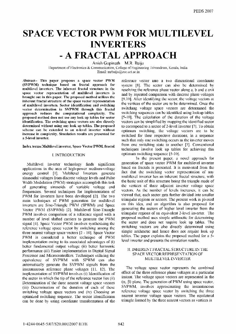
Fig. 1 (a) Voltage Space vectors of 2-level inverter (b) Voltage Spacevectors of 3-level inverter
referred as a sector. Fig. 1(a) shows the voltage spacevectors of 2-level inverter. The voltage space vectorlocations for a 3-level inverter are shown in Fig.1 (b)where Aoo, Ao1. A02, A03, A04, A05 and A06 are same aslocations of voltage space vectors of 2-level inverter.Consider the region marked I in the case of 2-levelinverter (Fig. l(a)), formed by the vectors located at Aoo,Ao1, and A02. In the case of 3-level inverter, as in Fig.1(b), this region has three additional voltage space vectors.It may be noted that the three additional voltage spacevectors are located at the midpoints of each side of thesector of equivalent 2-level inverter. The three additionalswitching voltage space vectors together with switchingvoltage space vectors located at Aoo, Ao1 and A02 results infour sectors within A AooAo1A02 of 3-level inverter.
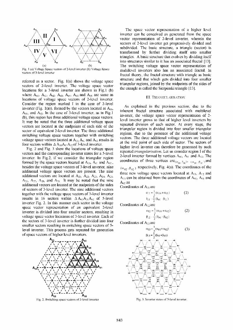
Fig. 2 and Fig. 3 show the locations of voltage spacevectors and the corresponding inverter states for a 5-levelinverter. In Fig.2, if we consider the triangular regionformed by the space vectors located at Aoo, Ao1 and A02,besides the voltage space vectors of 3-level inverter, nineadditional voltage space vectors are present. The nineadditional vectors are located at A21, A22, A23, A24, A25,A26, A27, A28, and A29. It may be noted that the nineadditional vectors are located at the midpoints of the sidesof sectors of 3-level inverter. The nine additional vectorstogether with the voltage space vectors of 3-level inverterresults in 16 sectors within A AooAo1A02 of 5-levelinverter Fig. 2. In this manner each sector in the voltagespace vector representation of an equivalent 2-levelinverter is divided into four smaller sectors, resulting involtage space vector locations of 3-level inverter. Each ofthe sectors of 3-level inverter is further divided into foursmaller sectors resulting in switching space vectors of 5-level inverter. This process gets repeated for generationof space vectors of higher level inverters.
A03 A02
/ \ ,I\ / \ / \ AX
/, \, \, \/ \, 2,A2 2 A
t-- - -X-- 3
'A2 1 2 01
I\ / \I/ \/ \ /\- - Y .-- -V - Y. -
A05 A06Fig. 2. Switching space vectors of 5-level inverter
The space vector representation of a higher levelinverter can be conceived as generated from the spacevector representation of 2-level inverter, wherein thesectors of 2-level inverter get progressively divided andsubdivided. The basic structure, a triangle (sector) istransformed by further dividing itself into smallertriangles. A basic structure that evolves by dividing itselfinto structures similar to it has an associated fractal [13].The switching voltage space vector representation ofmultilevel inverters also has an associated fractal. Infractal theory, the fractal structure with triangle as basicstructure and that which gets divided into four smallertriangular regions, joined by the midpoints of the sides ofthe triangle is called the Sierpinski triangle [13].
111. TRIANGULARISATION
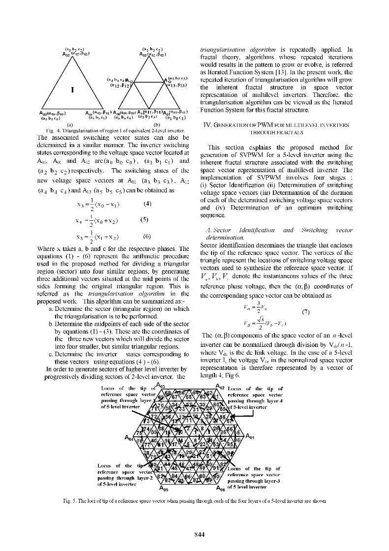
As explained in the previous section, due to theinherent fractal structure associated with multilevelinverter, the voltage space vector representation of 2-level inverter grows to that of higher level inverters byrepeated division of each sector. At every stage, thetriangular region is divided into four smaller triangularregions, due to the presence of the additional voltagevectors. The three additional voltage vectors are locatedat the mid point of each side of sector. The sectors ofhigher level inverter can therefore be generated by suchrepeated triangularisation. Let us consider region I of the2-level inverter formed by vertices Aoo, AO1 and A02. Thecoordinates of three vertices are(,,, 00), (xo 30Il ) and
(,x02 0) respectively, Fig. 4(a). The coordinates of the
three new voltage space vectors located at A1l, A12 andA13 can be obtained from the coordinates of Aoo, Ao1 andA02 asCoordinates of A1l are
ali I= 00 1+ a0 I)2
I2 (Poo +foI)
Coordinates ofA12 are
U12 2 (UOO +U02)
f12 =-2(O + P02)2Coordinates ofA13 are
(1 3 = I(co 1+ (X02)2
P13 = 2 (PO1I +-02)2
(1)
(2)
(3)
041 030 130 230 330 430141\0~241 \2/341 \20441\
/031/ -°3°/ \120 220 32i 420042 03 21 331 431142\ X 242 \1/342 \ i 442 \21 l
043 032 021 12- 22 321 31 4101332 232 323 42 421243 \011 34 \000~ 44 1,00,43\ \
033 02 122 1 211 200 300044 144 133 - 233 222 322 311 411 400
0/\12 4 13 \ 201 /22\03 123 112 212 312 301
034 134 34 22 3 4 412 401
013 113 213 313 302 402024 142 22 324 ,424\ /41 /
003 103 203 303 403014 114 214 314 414
F 04 104 204 304 404
Fig. 3. Inverter states of 5-level inverter.
843
(a2 b2 c2) (a2 b2 C2)A02 (C02,P02) A02 E02P02c)
(a4 b4 C4A12 (a b5 c5)/CE 12I P1al2 13,P13)
A00(CE00,P00) A 1(Cto1SPo)Aoo(ctoo,OO)Alfta11,P11)A 1(C01,P01)(ao bo co) 1a bl cl) (ao bo co) (3b3C3) °al bl cl)
(a) (b)Fig. 4. Triangularisation ofregion I of equivalent 2-level inverter.
The associated switching vector states can also bedetermined in a similar manner. The inverter switchingstates corresponding to the voltage space vector located atAoo, Ao1 and A02 are(ao bo cO), (a1 b1 c1) and(a2 b2 c2)respectively. The switching states of thenew voltage space vectors at A1l (a3 b3 c3), A12(a4 b4 c4)andA13 (a5 b5 c5)canbeobtainedas
X3 (xO +x1)X32X4 = I(XO +x2)
21
x5 =-(XI+X2)2
(4)
(5)
(6)
Where x takes a, b and c for the respective phases. Theequations (1) - (6) represent the arithmetic procedureused in the proposed method for dividing a triangularregion (sector) into four similar regions, by generatingthree additional vectors situated at the mid points of thesides forming the original triangular region. This isreferred as the triangularisation algorithm in theproposed work. This algorithm can be summarized as:-
a. Determine the sector (triangular region) on whichthe triangularisation is to be performed.
b. Determine the midpoints of each side of the sectorby equations (1) - (3). These are the coordinates ofthe three new vectors which will divide the sectorinto four smaller, but similar triangular regions.
c. Determine the inverter states corresponding tothese vectors using equations (4 ) - (6).
In order to generate sectors of higher level inverter byprogressively dividing sectors of 2-level inverter, the
Locus of the tip olreference space vectoipassing through layer-of 5-level inverter
AO4 I
Locus of the tipreference space vectorpassing through layer-2of 5-level inverter
triangularisation algorithm is repeatedly applied. Infractal theory, algorithms whose repeated iterationswould results in the pattern to grow or evolve, is referredas Iterated Function System [13]. In the present work, therepeated iteration of triangularisation algorithm will growthe inherent fractal structure in space vectorrepresentation of multilevel inverters. Therefore, thetriangularisation algorithm can be viewed as the IteratedFunction System for this fractal structure.
IV. GENERATION OF PWM FOR MULTILEVEL INVERTERSTHROUGH FRACTALS
This section explains the proposed method forgeneration of SVPWM for a 5-level inverter using theinherent fractal structure associated with the switchingspace vector representation of multilevel inverter. Theimplementation of SVPWM involves four stages;(i) Sector Identification (ii) Determination of switchingvoltage space vectors (iii) Determination of the durationof each of the determined switching voltage space vectorsand (iv) Determination of an optimum switchingsequence.
A. Sector Identification and Switching vectordetermination.
Sector identification determines the triangle that enclosesthe tip of the reference space vector. The vertices of thetriangle represent the locations of switching voltage spacevectors used to synthesize the reference space vector. IfV,Vb,, V denote the instantaneous values of the threereference phase voltage, then the (oc, f) coordinates ofthe corresponding space vector can be obtained as
Va V2
V (V VV# = 2(Vb -Vc )
(7)
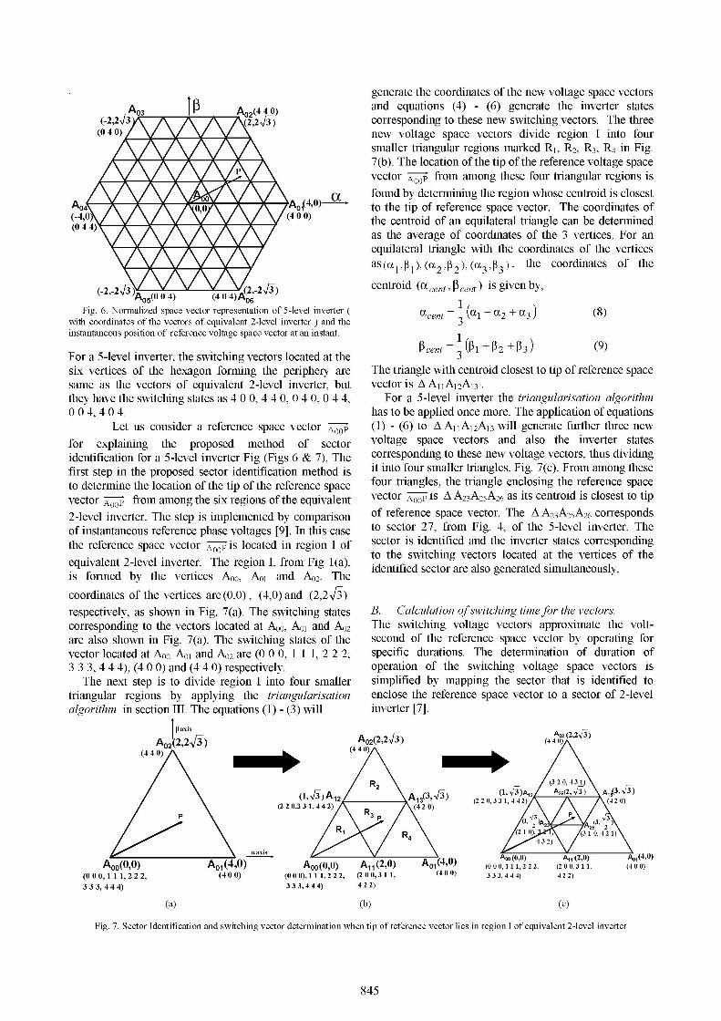
The (cc, f) components of the space vector of an n -levelinverter can be normalized through division by Vd,/ n -1,where Vd, is the dc link voltage. In the case of a 5-levelinverter I, the voltage Vd, in the normalized space vectorrepresentation is therefore represented by a vector oflength 4, Fig 6.
02 Locus of the tip ofreference space vector
passing through layer-4Df9O~'&-i(~n~'O f 5-level inverter
.7 Locus of the tip ofreference space vectorpassing through layer-3
A06 of 5-level inverter
Fig. 5. The loci of tip of a reference space vector when passing through each of the four layers of a 5 -level inverter are shown
844
A03 jf3 A02(4 4 0)(-2,2y3 2,2a3)
(O4V)
(-4X 09Ao 8 ~~~~~~~~~~40 0) a
(-2,-23 Ao 0 4) (4 0 4) -2$3)Fig. 6. Normalized space vector representation of 5-level inverter
with coordinates of the vectors of equivalent 2-level inverter ) and theinstantaneous position of reference voltage space vector at an instant.
For a 5-level inverter, the switching vectors located at thesix vertices of the hexagon forming the periphery aresame as the vectors of equivalent 2-level inverter, butthey have the switching states as 4 0 0, 4 4 0, 0 4 0, 0 4 4,O 040 4 0 4.
Let us consider a reference space vector AOOPfor explaining the proposed method of sectoridentification for a 5-level inverter Fig (Figs 6 & 7). Thefirst step in the proposed sector identification method isto determine the location of the tip of the reference spacevector A from among the six regions of the equivalent2-level inverter. The step is implemented by comparisonof instantaneous reference phase voltages [9]. In this casethe reference space vector AOO is located in region I ofequivalent 2-level inverter. The region I, from Fig l(a),is formed by the vertices Aoo, Ao1 and A02. Thecoordinates of the vertices are(0,0), (4,0) and (2,2Vi)respectively, as shown in Fig. 7(a). The switching statescorresponding to the vectors located at Aoo, Ao0 and A02are also shown in Fig. 7(a). The switching states of thevector located at Aoo, AO1 and A02 are (O 0 0, 11 1, 2 2 2,3 3 3, 4 4 4), (4 0 0) and (4 4 0) respectively.
The next step is to divide region I into four smallertriangular regions by applying the triangularisationalgorithm in section III. The equations (1) - (3) will
t,2J1)
generate the coordinates of the new voltage space vectorsand equations (4) - (6) generate the inverter statescorresponding to these new switching vectors. The threenew voltage space vectors divide region I into foursmaller triangular regions marked R1, R2, R3, R4 in Fig.7(b). The location ofthe tip ofthe reference voltage spacevector A from among these four triangular regions isfound by determining the region whose centroid is closestto the tip of reference space vector. The coordinates ofthe centroid of an equilateral triangle can be determinedas the average of coordinates of the 3 vertices. For anequilateral triangle with the coordinates of the verticesas (x1:1P) (oc2,J32), (oc3,J33), the coordinates of the
centroid (c cent' P cent ) is given by,
1acent = (aL1 +L2 +cL3 )
Pcent 13(p1 +p2 +j33)
(8)
(9)
The triangle with centroid closest to tip of reference spacevector is AA,1A12AI3.
For a 5-level inverter the triangularisation algorithmhas to be applied once more. The application of equations(1) - (6) to A Al1A12AI3 will generate further three newvoltage space vectors and also the inverter statescorresponding to these new voltage vectors, thus dividingit into four smaller triangles, Fig. 7(c). From among thesefour triangles, the triangle enclosing the reference spacevector A is A A23A25A26 as its centroid is closest to tipof reference space vector. The A A23A25A26 correspondsto sector 27, from Fig. 4, of the 5-level inverter. Thesector is identified and the inverter states correspondingto the switching vectors located at the vertices of theidentified sector are also generated simultaneously.
B. Calculation ofswitching timefor the vectors.The switching voltage vectors approximate the volt-second of the reference space vector by operating forspecific durations. The determination of duration ofoperation of the switching voltage space vectors issimplified by mapping the sector that is identified toenclose the reference space vector to a sector of 2-levelinverter [7].
A02(2,2V3)(440)A
0 0)3 3 3, 4 4 4)
(a) (b)
A02 (2,2 3)(440)
(320,431)(1, 3)A12 A26(2, a)\A,3(3,,\a)
(220,331,442) (420)
2 25)A(3,2(210), (3~1 0,421432)
oo (0,0) A11 (2,0) A01(4,0)(000,111,222, (200,311, (400)333,444) 422)
(c)
Fig. 7. Sector Identification and switching vector determination when tip of reference vector lies in region I of equivalent 2-level inverter
845
-
The mapping is done by choosing one of the three vectorsof the identified sector to coincide with the actual zerovector in the voltage space vector representation of theinverter. In the present work the vector selected tocoincide with the actual zero vector is referred as virtualzero vector. The vector with minimum value for the sumof magnitudes of oc and f coordinates is chosen to be thevirtual zero vector for a particular sector. The sum ofmagnitudes of cx and D coordinates represent the totaloffset of the vector from actual zero vector. Therefore, inthe present work the virtual zero vector chosen is atminimum offset from zero vector.For the voltage reference vectorA00 , the sectoridentified is sector 27. The voltage space vector with tiplocated at A23 becomes the virtual zero vector for sector27 . The sector 27 thus gets mapped to sector 1 (refer Fig.5) of the 5-level inverter. The determination of durationnow reduces to that of a 2-level inverter since aftermapping one of the vectors of the identified sectorcoincides with the zero vector. The durations of thevectors can be determined using the conventionalequations for 2-level inverter [3].
C. Determination ofoptimized switching sequence sOnce the switching vectors are determined and their
respective durations are calculated, then vectors are to beswitched in an optimum sequence such that only oneswitching occurs when the inverter changes its state. Inthe space phasor PWM technique, the optimum switchingis achieved by using the redundant states of the zerovector for alternate switching cycles. In the proposedwork, the optimum switching is achieved by using tworedundant switching states of the respective virtual zerovector in the alternate cycles.
The tip of the reference vector AOOP is located insector 27. The switching states corresponding to theswitching vectors at the vertices of sector 27 withredundancies are A23 (2 1 0, 3 2 1, 4 3 2), A25 (3 1 0, 4 21) and A26 (3 2 0, 4 3 1). For sector 27, the virtual zerovector at A23 has three redundant switching states whilethe voltage vectors at A25 and A26 has two redundancieseach. In the present work, ifthe redundancy ofthe virtualzero vector is greater than two, the last two redundantswitching states are selected for the virtual zero vector.For the other two vectors, if redundant states are morethan one, the last redundant state is selected. Thisstrategy of choosing the last two redundant states for thevirtual zero vector and the last redundant state for theother vectors will achieve optimum switching sequence.The selection will result in switching states [(3 2 1),(4 32)] for the virtual zero vector. The other vectors hasswitching states [(4 2 1)] and [(4 3 1)]. With these states,switching sequence of inverter for the sector number 27 is3 2 1-4 2 144 3 1-4 3 2 during a sampling intervaland 4 3 244 3 1-4 2 1-3 2 1 for the subsequentsampling interval. It may be noted that only oneswitching occurs as the inverter changes state.
To demonstrate this strategy further, let us consideranother sector, sector 7 of layer2 of Fig. 5. It may be
noted from Fig. 2 that sector 7 is formed by vertices A21,A1l and A23. From Fig. 3, the switching inverter statescorresponding to the vectors at these vertices are A21(1 00, 2 1 1, 3 2 2, 4 3 3), A11(2 0 0, 3 1 1, 4 2 2) andA23(2 10, 3 2 1, 4 3 2).The switching vector located at A21 is the virtual zerovector for sector 7. In this case, the virtual zero has fourredundant states (1 0 0, 2 1 1, 3 2 2, 4 3 3) and the othertwo vectors have three redundant states each. As per thestrategy adopted in the proposed work, the last tworedundant states are selected for the virtual zero vectori.e. (3 2 2, 4 3 3). For the other two vectors, among theirredundancies the last redundant state is selected i.e. forvector located at A11 state (4 2 2) and for the vector at A23state (4 3 2) are selected. With these states the sequenceof inverter switching will be 3 2 2-4 2 2-4 3 2-4 3 3for one sampling interval and 4 3 344 3 244 2 2-3 2 2for the subsequent sampling interval. It may be noted thatthis is optimum switching where only one switching isinvolved as the inverter changes state.
Therefore, in the proposed work, optimumswitching sequence is achieved by adopting a strategy ofselecting the switching state of the vectors from theavailable redundancies. This simple strategy of choosingthe switching states from the available redundant statesachieves optimum switching in every sector and hencedoes not require look up tables.
V. SIMULATION RESULTS
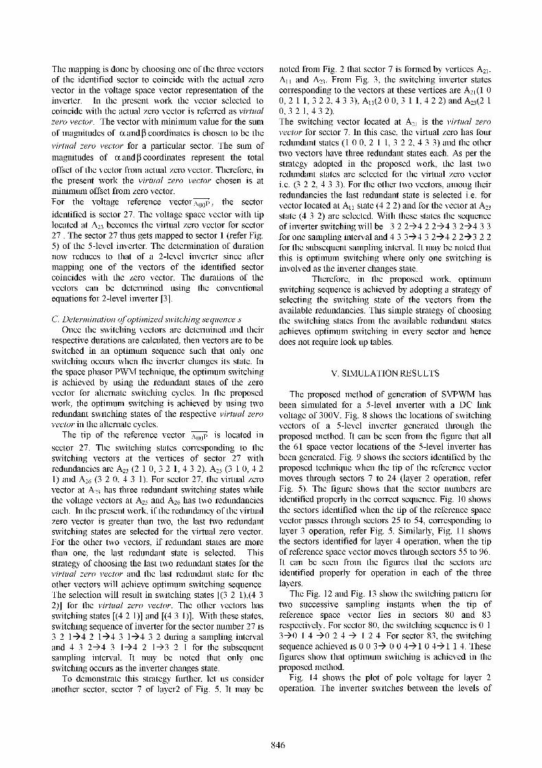
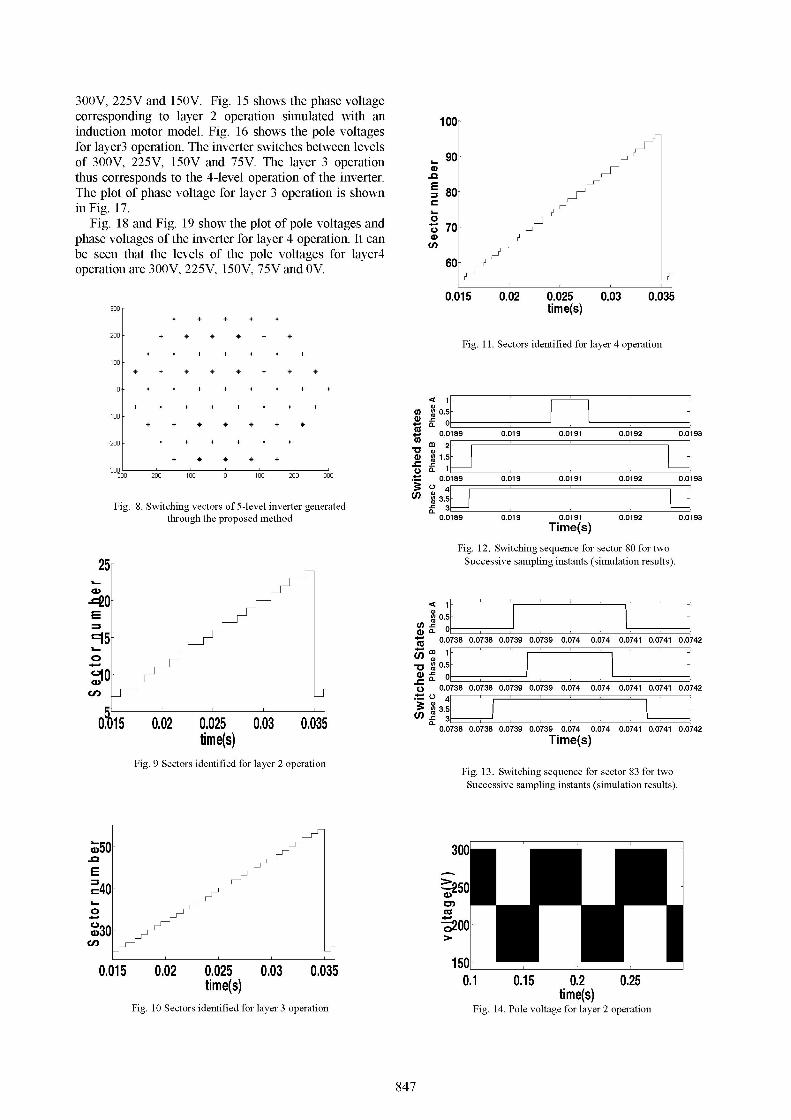
The proposed method of generation of SVPWM hasbeen simulated for a 5-level inverter with a DC linkvoltage of 300V. Fig. 8 shows the locations of switchingvectors of a 5-level inverter generated through theproposed method. It can be seen from the figure that allthe 61 space vector locations of the 5-level inverter hasbeen generated. Fig. 9 shows the sectors identified by theproposed technique when the tip of the reference vectormoves through sectors 7 to 24 (layer 2 operation, referFig. 5). The figure shows that the sector numbers areidentified properly in the correct sequence. Fig. 10 showsthe sectors identified when the tip of the reference spacevector passes through sectors 25 to 54, corresponding tolayer 3 operation, refer Fig. 5. Similarly, Fig. 11 showsthe sectors identified for layer 4 operation, when the tipof reference space vector moves through sectors 55 to 96.It can be seen from the figures that the sectors areidentified properly for operation in each of the threelayers.
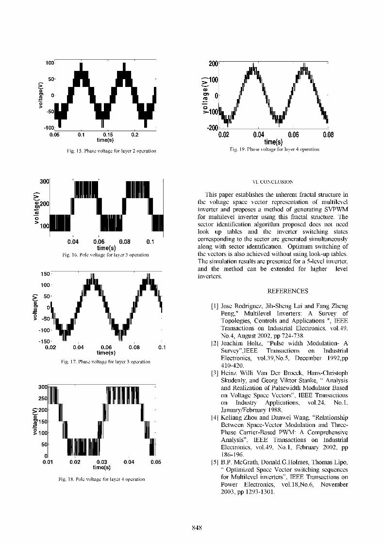
The Fig. 12 and Fig. 13 show the switching pattern fortwo successive sampling instants when the tip ofreference space vector lies in sectors 80 and 83respectively. For sector 80, the switching sequence is 0 1340 1 4 -0 2 4 e 1 2 4. For sector 83, the switchingsequence achieved is 0 0 3- 0 0 4-1 0 4-1 1 4. Thesefigures show that optimum switching is achieved in theproposed method.
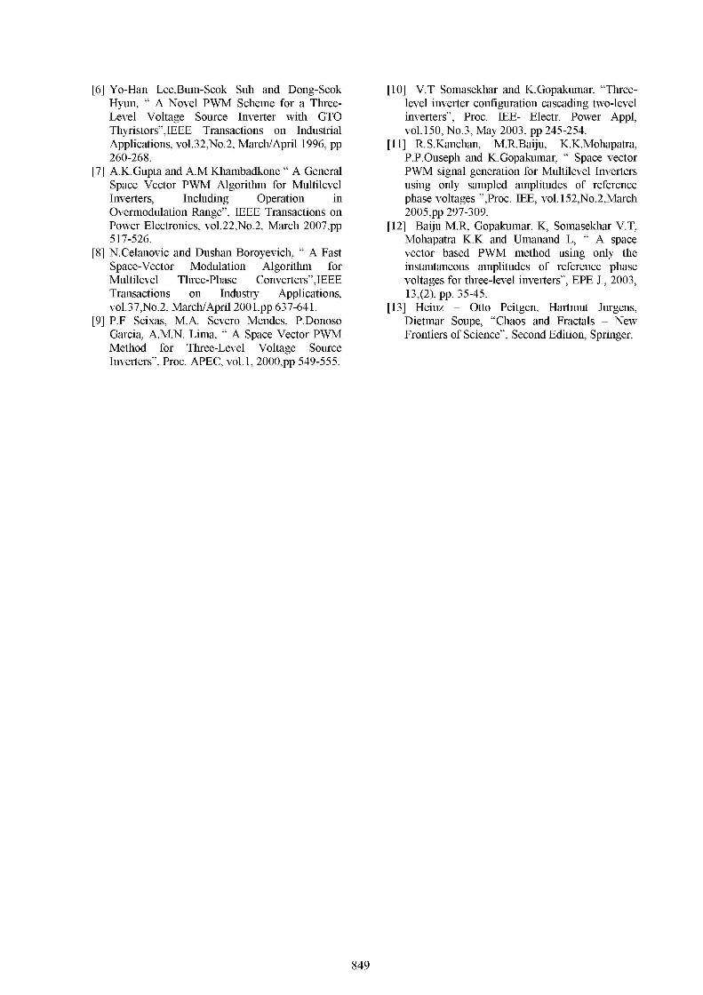
Fig. 14 shows the plot of pole voltage for layer 2operation. The inverter switches between the levels of
846
300V, 225V and 150V. Fig. 15 shows the phase voltagecorresponding to layer 2 operation simulated with aninduction motor model. Fig. 16 shows the pole voltagesfor layer3 operation. The inverter switches between levelsof 300V, 225V, 150V and 75V. The layer 3 operationthus corresponds to the 4-level operation of the inverter.The plot of phase voltage for layer 3 operation is shownin Fig. 17.
Fig. 18 and Fig. 19 show the plot of pole voltages andphase voltages of the inverter for layer 4 operation. It canbe seen that the levels of the pole voltages for layer4operation are 300V, 225V, 150V, 75V and OV.
200
100
-100
-200
* * * * *
* * * * * *
* * * * * * *
* * * * * * * *
* * * * * * * *
+ + + + + + + +
* * * * * * *
* * * * * *
* * * * *
Fig. 8. Switching vectors of 5-level inverter generatedthrough the proposed method
100
" 90-90EF 80
0o 70a,)cn
60~
0.015 0.02 0.025 0.03 0.035time(s)
Fig. 11. Sectors identified for layer 4 operation
0.5-
0.0189 0.019 0.0191 0.0192 0.0193
211 X
. 0.0189 0.019 0.0191 0.0192 0.0193L)4-
-3.50.0189 0.019 0.0191 0.0192 0.0193
Time(s)Fig. 12. Switching sequence for sector 80 for two
25 Successive sampling instants (simulation results).
E
-15
cn X
0.15 0.02 0.025 0.03 0.035time(s)
Fig. 9 Sectors identified for layer 2 operation
eD50-oE040,L..
0
030,cn ~~~I
0.015 0.02 0.025 0.03 0.035time(s)
Fig. 10 Sectors identified for layer 3 operation
0.5.
sS 0.0738 0.0738 0.0739 0.0739 0.074 0.074 0.0741 0.0741 0.0742
0.
0.0738 0.0738 0.0739 0.0739 0.074 0.074 0.0741 0.0741 0.0742u)°v0.5-s
0.0738 0.0738 0.0739 0.0739 0.074 0.074 0.0741 0.0741 0.0742Time(s)
Fig. 13. Switching sequence for sector 83 for two
Successive sampling instants (simulation results).
0.1 0.15 0.2 0.25time(s)
Fig. 14. Pole voltage for layer 2 operation
847
-300 ' I I I I I~~~~~~~~~~~~~~~~~~~~~~~~~~~~~~~~~~~~~~~~~~~~~~~~~~~~~~~~~~~~
100
0.1 0.15 0.2
time(s)
Fig. 15. Phase voltage for layer 2 operation
0.02 0.04 0.06time(s)
Fig. 19. Phase voltage for layer 4 operation
I JI
0.04 0.06 0.08 0.1time(s)
Fig. 16. Pole voltage for layer 3 operation
150F
0-
(g0
0.04 0.06 0.08time(s)
Fig. 17. Phase voltage for layer 3 operation
VI. CONCLUSION
This paper establishes the inherent fractal structure inthe voltage space vector representation of multilevelinverter and proposes a method of generating SVPWMfor multilevel inverter using this fractal structure. Thesector identification algorithm proposed does not needlook up tables and the inverter switching statescorresponding to the sector are generated simultaneouslyalong with sector identification. Optimum switching ofthe vectors is also achieved without using look-up tables.The simulation results are presented for a 5-level inverter,and the method can be extended for higher levelinverters.
REFERENCES
[1] Jose Rodriguez, Jih-Sheng Lai and Fang ZhengPeng," Multilevel Inverters: A Survey ofTopologies, Controls and Applications ", IEEETransactions on Industrial Electronics, vol.49,No.4, August 2002, pp 724-738.
[2] Joachim Holtz, "Pulse width Modulation- ASurvey",IEEE Transactions on IndustrialElectronics, vol.39,No.5, December 1992,pp410-420.
[3] Heinz Willi Van Der Broeck, Hans-ChristophSkudenly, and Georg Viktor Stanke, " Analysisand Realization of Pulsewidth Modulator Basedon Voltage Space Vectors", IEEE Transactionson Industry Applications, vol.24, No.1,January/February 1988.
[4] Keliang Zhou and Danwei Wang, "RelationshipBetween Space-Vector Modulation and Three-Phase Carrier-Based PWM: A ComprehensiveAnalysis", IEEE Transactions on IndustrialElectronics, vol.49, No.1, February 2002, pp186-196.
[5] B.P. McGrath, Donald.G.Holmes, Thomas Lipo," Optimized Space Vector switching sequencesfor Multilevel inverters", IEEE Transactions onPower Electronics, vol.18,No.6, November2003, pp 1293-1301.
0.1
0.01 0.02 0.03 0.04 0.05time(s)
Fig. 18. Pole voltage for layer 4 operation
848
a1)m o.
0
-50
-1000.05
300F
0.08
(,200
o |100I
-100 11111
-1500.02
200f
[6] Yo-Han Lee,Bum-Seok Suh and Dong-SeokHyun, " A Novel PWM Scheme for a Three-Level Voltage Source Inverter with GTOThyristors",IEEE Transactions on IndustrialApplications, vol.32,No.2, March/April 1996, pp260-268.
[7] A.K.Gupta and A.M Khambadkone " A GeneralSpace Vector PWM Algorithm for MultilevelInverters, Including Operation inOvermodulation Range", IEEE Transactions onPower Electronics, vol.22,No.2, March 2007,pp517-526.
[8] N.Celanovic and Dushan Boroyevich, " A FastSpace-Vector Modulation Algorithm forMultilevel Three-Phase Converters",IEEETransactions on Industry Applications,vol.37,No.2, March/April 2001,pp 637-641.
[9] P.F Seixas, M.A. Severo Mendes, P.DonosoGarcia, A.M.N. Lima, " A Space Vector PWMMethod for Three-Level Voltage SourceInverters", Proc. APEC, vol.1, 2000,pp 549-555.
[10] V.T Somasekhar and K.Gopakumar, "Three-level inverter configuration cascading two-levelinverters", Proc. IEE- Electr. Power Appl,vol.150, No.3, May 2003, pp 245-254.
[11] R.S.Kanchan, M.R.Baiju, K.K.Mohapatra,P.P.Ouseph and K.Gopakumar, " Space vectorPWM signal generation for Multilevel Invertersusing only sampled amplitudes of referencephase voltages ",Proc. IEE, vol.152,No.2,March2005,pp 297-309.
[12] Baiju M.R, Gopakumar. K, Somasekhar V.T,Mohapatra K.K and Umanand L, " A spacevector based PWM method using only theinstantaneous amplitudes of reference phasevoltages for three-level inverters", EPE J., 2003,13,(2), pp. 35-45.
[13] Heinz - Otto Peitgen, Hartmut Jurgens,Dietmar Soupe, "Chaos and Fractals - NewFrontiers of Science", Second Edition, Springer.
849