Using PWM Output as a Digital-to-Analog Converter ... - EDGE
Upload
khangminh22Category
view
0download
0
PWM Converter for a Highly
Non-Linear Plasma Load
By
Wim van der Merwe
Thesis presented in partial fulfilment of the requirements for the
degree of Master of Science (Engineering) at the University of
Stellenbosch
Supervisors:
Prof H Du T Mouton
Prof P.H. Swart
November 29, 2005

Declaration
I, the undersigned, hereby declare that the work contained in this thesis is my own
original work, unless otherwise stated, and has not previously, in its entirety or in part,
been admitted at any university for a degree.
...................................
Wim van der Merwe
November 29, 2005
i

“Happy is the man who can recognise in the work of today a connected portion of the work
of life, and an embodiment of the work of Eternity . . . ”
James Clerk Maxwell
ii

Summary
This thesis discuss an investigation into the applicability of modern high frequency power
conversion technology in the plasma mineral processing industry. The physics governing
the plasma in a processing environment are analysed to provide a clear understanding
of this plasma as electrical load. This was done to create an electrical model for the
plasma as load and gain understanding into the electrical supply requirements. Modern
high frequency power conversion technology is contrasted with thyristor controlled line
frequency technologies to provide a suitable starting point for the study. A 3 kW soft
switched converter is proposed for application with a plasma load. This converter is
designed and verified. The small-signal signature of the proposed converter under peak
current mode control is investigated and a new model is proposed to describe this control
configuration.
iii

Opsomming
Hierdie tesis bespreek ’n lewensvatbaarheids studie van moderne hoe frekwensie drywings
omsetters in the plasma mineraal verwerkings industrie. Die fisika van die plasma in die
mineraal verwerkings omgewing word ondersoek sodat die plasma as elektriese las beskryf
kan word. Hoe frekwensie drywings omsetters word vergelyk met die huidige lynfrekwensie
tegnologie ten einde ’n logiese vertrek punt vir die studie te verkry. ’n 3 kW hoe frekwensie
sag geskakelde omsetter word voorgestel vir gebruik met ’n plasma las. Die omsetter word
ontwerp en geverifieer. Die klein sein analiese van die voorgestelde omsetter onder piek
stroom beheer word ondersoek en ’n nuwe model word voorgestel om die omsetter-beheer
kombinasie te beskryf.
iv

Acknowledgments
I would like to thank the following people:
Prof. Mouton and Prof. Swart, my supervisors. Thank you for your time and effort.
Everyone who made this project possible financially. Thermtron, NECSA and the DASC
Consortium. Kokkie for the initiation into plasma processing.
My colleagues at TuT Power Engineering. Dawie, thank you for the opportunity and for
understanding. Kobus for providing valuable support. Cecil, a conversation with you is
always interesting.
My old colleagues at Power Electronics, Kentron. Especially George, Rex and Rob. To
be honest, about all I know about power electronic development I’ve learned from you.
Rex, thank you for your support with the current sensing.
Thinus, thank you for your valuable contributions and proof reading this document.
My parents and sisters, I don’t thank you often enough.
The nameless, faceless multitudes who contributed to LATEX and MikTex. I cannot imagine
doing this in. . .
Everyone at Shofar Pretoria. Thanks guys.
All my friends who helped me through this. Albert, Anthea, Barry, Christo, Corne,
Hendrik, Hercu & Minette, Ira, Jacques, Philip & Nicola, Ross & Magriet, SG, Theo,
Vivian and everyone else, I’m running out of space. Thank you for your prayers and
support. Belangrikste van alles, julle het verstaan.
The Triune God. Thank You for being here. You are always true to who You are; Faithful.
v

Contents
1 Plasma Technology and Modern Society 1
1.1 Plasmas and Nature . . . . . . . . . . . . . . . . . . . . . . . . . . . . . . 1
1.2 Everyday Use of Plasmas . . . . . . . . . . . . . . . . . . . . . . . . . . . . 3
1.3 Waste Treatment . . . . . . . . . . . . . . . . . . . . . . . . . . . . . . . . 3
1.4 Unconventional Uses of Plasmas . . . . . . . . . . . . . . . . . . . . . . . . 5
1.5 Industrial Processing . . . . . . . . . . . . . . . . . . . . . . . . . . . . . . 5
1.5.1 Plasma Processing in South Africa . . . . . . . . . . . . . . . . . . 6
1.6 Plasma Electronics . . . . . . . . . . . . . . . . . . . . . . . . . . . . . . . 7
1.7 Study Aim . . . . . . . . . . . . . . . . . . . . . . . . . . . . . . . . . . . . 7
2 The Plasma as Electrical Load 8
2.1 Plasma Dynamics . . . . . . . . . . . . . . . . . . . . . . . . . . . . . . . . 8
2.1.1 Ionization . . . . . . . . . . . . . . . . . . . . . . . . . . . . . . . . 8
2.1.2 Boundary Conditions of Plasma Existence . . . . . . . . . . . . . . 9
2.1.3 Collective Plasma Behaviour and Instabilities . . . . . . . . . . . . 10
2.2 Behaviour as Electrical Load . . . . . . . . . . . . . . . . . . . . . . . . . . 14
2.2.1 Variations in Effective Resistance . . . . . . . . . . . . . . . . . . . 14
2.2.2 Generalised Arc Resistance Variation Model . . . . . . . . . . . . . 17
2.2.3 Requirements of the Power Converter . . . . . . . . . . . . . . . . . 17
3 Electric Topology 19
3.1 Line Frequency Technologies . . . . . . . . . . . . . . . . . . . . . . . . . . 19
3.1.1 Output Inductor Considerations . . . . . . . . . . . . . . . . . . . . 20
3.1.2 Harmonic Pollution . . . . . . . . . . . . . . . . . . . . . . . . . . . 22
3.1.3 Isolation Transformer Considerations . . . . . . . . . . . . . . . . . 23
3.1.4 Control Considerations . . . . . . . . . . . . . . . . . . . . . . . . . 24
3.1.5 Conclusion . . . . . . . . . . . . . . . . . . . . . . . . . . . . . . . . 24
3.2 High Frequency Topology Selection . . . . . . . . . . . . . . . . . . . . . . 25
3.2.1 Full-Bridge versus Other Topologies . . . . . . . . . . . . . . . . . . 25
vi

CONTENTS vii
3.2.2 ZVS Full-Bridge Topologies . . . . . . . . . . . . . . . . . . . . . . 26
3.3 The Leakage Inductance ZVS Phase Shifted Full-Bridge . . . . . . . . . . . 29
3.3.1 Operational Principle . . . . . . . . . . . . . . . . . . . . . . . . . . 30
3.4 Converter Operation . . . . . . . . . . . . . . . . . . . . . . . . . . . . . . 32
3.4.1 State II, Power Transfer . . . . . . . . . . . . . . . . . . . . . . . . 32
3.4.2 State III, Right Leg Transition . . . . . . . . . . . . . . . . . . . . 35
3.4.3 State IV, Current Free Flow . . . . . . . . . . . . . . . . . . . . . . 39
3.4.4 State V, Left Leg Transition . . . . . . . . . . . . . . . . . . . . . . 40
3.4.5 State VI, Current Commutation . . . . . . . . . . . . . . . . . . . . 42
3.4.6 State VII, Power Transfer . . . . . . . . . . . . . . . . . . . . . . . 43
3.4.7 Model Validation . . . . . . . . . . . . . . . . . . . . . . . . . . . . 43
3.5 Secondary Rectifiers . . . . . . . . . . . . . . . . . . . . . . . . . . . . . . 44
3.6 Current Doubling Rectifier . . . . . . . . . . . . . . . . . . . . . . . . . . . 45
3.6.1 Operation . . . . . . . . . . . . . . . . . . . . . . . . . . . . . . . . 47
3.6.2 Center Tapped Rectifier . . . . . . . . . . . . . . . . . . . . . . . . 49
4 System Design 50
4.1 Full Bridge . . . . . . . . . . . . . . . . . . . . . . . . . . . . . . . . . . . 50
4.1.1 Switch Element Dimensioning . . . . . . . . . . . . . . . . . . . . . 52
4.1.2 ZVS Implementation . . . . . . . . . . . . . . . . . . . . . . . . . . 53
4.1.3 Slope Compensation . . . . . . . . . . . . . . . . . . . . . . . . . . 54
4.2 Output Inductance . . . . . . . . . . . . . . . . . . . . . . . . . . . . . . . 55
4.2.1 Output Current Ripple . . . . . . . . . . . . . . . . . . . . . . . . . 55
4.2.2 Inductor Losses . . . . . . . . . . . . . . . . . . . . . . . . . . . . . 60
4.3 Output Capacitance . . . . . . . . . . . . . . . . . . . . . . . . . . . . . . 64
4.4 Transformer Design . . . . . . . . . . . . . . . . . . . . . . . . . . . . . . . 64
4.4.1 Transformer Saturation . . . . . . . . . . . . . . . . . . . . . . . . . 64
4.4.2 Transformer Losses . . . . . . . . . . . . . . . . . . . . . . . . . . . 65
4.5 Boost Rectifier Design . . . . . . . . . . . . . . . . . . . . . . . . . . . . . 66
4.5.1 Power Stage Design . . . . . . . . . . . . . . . . . . . . . . . . . . . 66
4.5.2 Control Loop . . . . . . . . . . . . . . . . . . . . . . . . . . . . . . 70
4.5.3 Inner Current Control Loop Compensation . . . . . . . . . . . . . . 70
4.5.4 Outer Voltage Loop Compensation . . . . . . . . . . . . . . . . . . 74
4.5.5 Current Sensing and System Setup . . . . . . . . . . . . . . . . . . 79
4.6 Bias Supplies . . . . . . . . . . . . . . . . . . . . . . . . . . . . . . . . . . 80
4.7 75 kW Interface . . . . . . . . . . . . . . . . . . . . . . . . . . . . . . . . . 81
4.8 PCB Layout . . . . . . . . . . . . . . . . . . . . . . . . . . . . . . . . . . . 82
4.8.1 Control Board . . . . . . . . . . . . . . . . . . . . . . . . . . . . . . 82
4.8.2 Power Board . . . . . . . . . . . . . . . . . . . . . . . . . . . . . . 83

CONTENTS viii
5 Control System Design 85
5.1 Current Control Schemes . . . . . . . . . . . . . . . . . . . . . . . . . . . 85
5.1.1 Peak Current Mode Control . . . . . . . . . . . . . . . . . . . . . . 87
5.1.2 Average Current Mode Control . . . . . . . . . . . . . . . . . . . . 88
5.1.3 Average versus Peak Current Mode in a ZVS FB Converter . . . . . 89
5.2 Small-Signal Modelling of Current Mode Control . . . . . . . . . . . . . . . 90
5.2.1 Small-Signal Current Modulator Gain . . . . . . . . . . . . . . . . . 90
5.2.2 The Discretisation of the Error-Signal . . . . . . . . . . . . . . . . . 92
5.2.3 Representation of He(s) in the System Model . . . . . . . . . . . . 95
5.3 Modelling of the ZVS Full-Bridge Converter under Peak Current Control . 98
5.3.1 Derivation of the Transfer Functions . . . . . . . . . . . . . . . . . 98
5.3.2 Derivation of the System Transfer Function . . . . . . . . . . . . . 102
5.4 An Alternative Cross-Coupled Signal Model . . . . . . . . . . . . . . . . . 104
5.5 Slope Compensation . . . . . . . . . . . . . . . . . . . . . . . . . . . . . . 110
6 System Evaluation 112
6.1 Bias Supply Flyback Converter . . . . . . . . . . . . . . . . . . . . . . . . 112
6.1.1 Control System and Stability . . . . . . . . . . . . . . . . . . . . . 112
6.1.2 Electro-Magnetic Compatibility . . . . . . . . . . . . . . . . . . . . 115
6.2 Power Factor Correction Boost Rectifier . . . . . . . . . . . . . . . . . . . 117
6.3 ZVS Phase Shifted Full-Bridge . . . . . . . . . . . . . . . . . . . . . . . . . 119
6.3.1 Transformer Characterisation . . . . . . . . . . . . . . . . . . . . . 119
6.3.2 Output Rectifier Diode Ringing . . . . . . . . . . . . . . . . . . . . 125
6.3.3 Verification of the Parasitics Measurements . . . . . . . . . . . . . . 128
6.3.4 Output Step Response . . . . . . . . . . . . . . . . . . . . . . . . . 130
6.3.5 General Tests and Plasma Loads . . . . . . . . . . . . . . . . . . . 131
7 Conclusion 136
7.1 Summary of Study . . . . . . . . . . . . . . . . . . . . . . . . . . . . . . . 136
7.1.1 Main Contributions . . . . . . . . . . . . . . . . . . . . . . . . . . . 136
7.2 Conclusions . . . . . . . . . . . . . . . . . . . . . . . . . . . . . . . . . . . 137
7.3 Further Work . . . . . . . . . . . . . . . . . . . . . . . . . . . . . . . . . . 138
A Mathematical Derivations 144
A.1 Averaged Switch Network for Buck Converter . . . . . . . . . . . . . . . . 145
A.2 State Space Averaging of the Current Doubler . . . . . . . . . . . . . . . . 147
A.3 State Space Averaging of the Center Tap Rectifier . . . . . . . . . . . . . . 153
A.4 Circuit behaviour . . . . . . . . . . . . . . . . . . . . . . . . . . . . . . . . 156
A.4.1 Output Current Ripple . . . . . . . . . . . . . . . . . . . . . . . . . 156

CONTENTS ix
A.5 Magnetics . . . . . . . . . . . . . . . . . . . . . . . . . . . . . . . . . . . . 158
A.5.1 DC Bias - Inductance Relationship . . . . . . . . . . . . . . . . . . 158
A.5.2 Transformer Saturation . . . . . . . . . . . . . . . . . . . . . . . . . 159
B ZVS-FB Mathcad Analysis 160
C Bias Flyback Design Documentation 174
D PFC Boost Rectifier Design Documents 182
E Magnetic Design Spreadsheets 194
F Selected MATLAB simulation M-files 197
F.1 CDR and CTR Ripple Current Copper Loss . . . . . . . . . . . . . . . . . 197
F.2 Transformer Short Circuit Test . . . . . . . . . . . . . . . . . . . . . . . . 199
F.3 Output Diode Ringing Waveforms and Snubber Design . . . . . . . . . . . 202
G Schematics, Manufacturing Drawings and Documentation 206

List of Figures
1.1 St. Elmo’s Fire . . . . . . . . . . . . . . . . . . . . . . . . . . . . . . . . . 2
2.1 Discharge Instabilities . . . . . . . . . . . . . . . . . . . . . . . . . . . . . 11
2.2 Plasma Element in a Homogeneous Magnetic Field . . . . . . . . . . . . . 12
2.3 Flute Instability . . . . . . . . . . . . . . . . . . . . . . . . . . . . . . . . . 13
2.4 Shunting in a Linear dc Plasma Torch . . . . . . . . . . . . . . . . . . . . 13
3.1 Single Line Diagram of a 12-Pulse Rectifier . . . . . . . . . . . . . . . . . . 20
3.2 Preloading the Output Filter Inductor . . . . . . . . . . . . . . . . . . . . 21
3.3 ZVS Full-Bridge with Added Parasitic Elements . . . . . . . . . . . . . . . 27
3.4 The Phase Shift Between the Half-Legs of the ZVS-FB . . . . . . . . . . . 28
3.5 The Leakage Inductance ZVS-FB with CDR . . . . . . . . . . . . . . . . . 29
3.6 Time Waveforms of the ZVS Phase Shifted Full-Bridge . . . . . . . . . . . 31
3.8 ZVS FB State II . . . . . . . . . . . . . . . . . . . . . . . . . . . . . . . . 32
3.7 Conduction States in the ZVS-FB . . . . . . . . . . . . . . . . . . . . . . . 34
3.9 ZVS FB State III . . . . . . . . . . . . . . . . . . . . . . . . . . . . . . . . 35
3.10 Typical Ringing Voltage and Current Waveforms Associated with State III 37
3.11 Operational Waveforms of ZVS-FB used to validate state III . . . . . . . . 38
3.12 Waveforms of the Right-Hand Transition During State III of the ZVS-FB . 39
3.13 ZVS FB State IV . . . . . . . . . . . . . . . . . . . . . . . . . . . . . . . . 39
3.14 ZVS FB State V . . . . . . . . . . . . . . . . . . . . . . . . . . . . . . . . 40
3.15 Incomplete Voltage Transition During State V . . . . . . . . . . . . . . . . 41
3.16 Incomplete Resonant Transition Half-Leg Voltage and Current Waveforms 41
3.17 State V Transition with Dead Time Chosen at Optimal Value . . . . . . . 42
3.18 ZVS FB State VI . . . . . . . . . . . . . . . . . . . . . . . . . . . . . . . . 43
3.19 ZVS FB State VII . . . . . . . . . . . . . . . . . . . . . . . . . . . . . . . 43
3.20 Measured Primary Current . . . . . . . . . . . . . . . . . . . . . . . . . . . 44
3.21 Calculated Primary Current . . . . . . . . . . . . . . . . . . . . . . . . . . 45
3.22 Current Doubling Rectifier . . . . . . . . . . . . . . . . . . . . . . . . . . . 45
x

LIST OF FIGURES xi
3.23 Current Doubler: Early Twentieth Century . . . . . . . . . . . . . . . . . . 46
3.24 Current Waveforms of the Doubling Rectifier Under CCM . . . . . . . . . 46
3.25 Conduction States in the Current Doubling Rectifier . . . . . . . . . . . . 48
3.26 Conduction States in the Current Doubling Rectifier . . . . . . . . . . . . 48
3.27 Center Tapped Rectifier . . . . . . . . . . . . . . . . . . . . . . . . . . . . 49
4.1 Block Diagram of the Complete System . . . . . . . . . . . . . . . . . . . . 51
4.2 Output Current Ripple vs Output Voltage (Vin = 400V ) . . . . . . . . . . 56
4.3 Typical B-H Curve for a Ferrite . . . . . . . . . . . . . . . . . . . . . . . . 57
4.4 Output Current Waveforms of the Center Tap Rectifier . . . . . . . . . . . 57
4.5 Output Current Waveforms of the Current Doubling Rectifier . . . . . . . 58
4.6 κ vs ∆I0 for CDR and CTR . . . . . . . . . . . . . . . . . . . . . . . . . . 60
4.7 Relative Losses of the CTR and CDR Ripple Current . . . . . . . . . . . . 63
4.8 Boost-Rectifier Power Circuit . . . . . . . . . . . . . . . . . . . . . . . . . 67
4.9 PFC Rectifier Two Loop Control Block Diagram . . . . . . . . . . . . . . . 71
4.10 Block Diagram of the Average Current Mode Current Loop in the PFC
Rectifier . . . . . . . . . . . . . . . . . . . . . . . . . . . . . . . . . . . . . 72
4.11 Open Loop Frequency Response of the Open Loop PFC Current Loop . . . 74
4.12 Step Response of the PFC-Boost Compensated Current Loop . . . . . . . 75
4.13 Frequency Response of the PFC Rectifier Voltage Loop Without the Ad-
dition of a Zero . . . . . . . . . . . . . . . . . . . . . . . . . . . . . . . . . 77
4.14 Frequency Response of the PFC Voltage Loop with the Addition of a Zero 78
4.15 Step Response of the PFC Rectifier Closed-Loop Voltage Loop . . . . . . . 78
4.16 Root Locus of the PFC Rectifier Voltage Loop . . . . . . . . . . . . . . . . 79
5.1 Hysteresis Peak Current Mode Circuit used by Hertz in 1888 . . . . . . . . 86
5.2 Peak Current Mode Control . . . . . . . . . . . . . . . . . . . . . . . . . . 87
5.3 Average Current Mode Control . . . . . . . . . . . . . . . . . . . . . . . . 88
5.4 Perturbation Waveforms under PCMC . . . . . . . . . . . . . . . . . . . . 91
5.5 Instability with d > 0.5 and no Slope Compensation . . . . . . . . . . . . . 93
5.6 Discretisation of the Error Signal in PCMC . . . . . . . . . . . . . . . . . 93
5.7 Simplified Block Diagram of PCMC . . . . . . . . . . . . . . . . . . . . . . 94
5.8 Frequency Response of H22(s), H12(s) and H14(s) . . . . . . . . . . . . . . 96
5.9 Step Response of H22(s), H12(s) and H14(s) . . . . . . . . . . . . . . . . . 97
5.10 Frequency Response of He(s) and Approximating Functions . . . . . . . . 97
5.11 ZVS Full-Bridge Topology . . . . . . . . . . . . . . . . . . . . . . . . . . . 98
5.12 Equivalent Circuit of ZVS FB under Transient Conditions . . . . . . . . . 99
5.13 Block Diagram of the ZVS-FB under PCMC . . . . . . . . . . . . . . . . . 99
5.14 Bode Plot of the Derived Transfer Functions . . . . . . . . . . . . . . . . . 101

LIST OF FIGURES xii
5.15 Comparison of the Derived Forward Transfer Function and the Transfer
Function Proposed by Kutkut . . . . . . . . . . . . . . . . . . . . . . . . . 102
5.16 Comparison of the Derived Cross Transfer Function and the Transfer Func-
tion Proposed by Kutkut . . . . . . . . . . . . . . . . . . . . . . . . . . . . 103
5.17 Signal Flow Diagram for the ZVS-FB under PCMC . . . . . . . . . . . . . 103
5.18 Average Inductor Current under PCMC . . . . . . . . . . . . . . . . . . . 105
5.19 Cross-Coupling Between the Two PCM Loops in Time . . . . . . . . . . . 106
5.20 Simplorer Model to Investigate the Cross-Coupling . . . . . . . . . . . . . 107
5.21 Modified Block Diagram to Account for Ripple Cross Coupling . . . . . . . 108
5.22 Simplorer and Simulink Simulated Currents for the Forward Transfer Func-
tion . . . . . . . . . . . . . . . . . . . . . . . . . . . . . . . . . . . . . . . 108
5.23 Simplorer and Simulink Simulated Currents for the Cross-Coupled Transfer
Functions . . . . . . . . . . . . . . . . . . . . . . . . . . . . . . . . . . . . 109
5.24 Block Diagram of a Buck Converter Under PCMC . . . . . . . . . . . . . . 110
5.25 Open Loop Frequency Response of a Buck Converter Under PCMC with
Fm = 1 . . . . . . . . . . . . . . . . . . . . . . . . . . . . . . . . . . . . . . 111
6.1 Flyback Sensed Magnetising Current Information . . . . . . . . . . . . . . 113
6.2 Open Loop Bode Plot of the Flyback Bias Supply . . . . . . . . . . . . . . 114
6.3 Closed Loop Step Response of the Flyback Converter . . . . . . . . . . . . 115
6.4 Flyback Switch Drain-Source Voltage at the Turn-Off Transient with and
without the Snubber . . . . . . . . . . . . . . . . . . . . . . . . . . . . . . 116
6.5 Differential Mode Noise on the Flyback Output Signal . . . . . . . . . . . 117
6.6 Input Current to the Rectifier with and without the Active Boost . . . . . 118
6.7 FFT of the Input Current without the Active Boost . . . . . . . . . . . . . 118
6.8 FFT of the Input Current with the Active Boost Converter . . . . . . . . . 119
6.9 Measured Waveforms of the Short-Circuit Test . . . . . . . . . . . . . . . . 120
6.10 FFT of the Primary Current Signal, With Selected Harmonics Indicated . 122
6.11 FFT of the Primary Voltage, With Selected Harmonics Indicated . . . . . 123
6.12 The Approximated Time Signal Versus the Original Signal . . . . . . . . . 124
6.13 Measured Leakage Inductance . . . . . . . . . . . . . . . . . . . . . . . . . 124
6.14 Waveforms Displaying The Transient Output Diode Ring . . . . . . . . . . 125
6.15 Equivalent Parasitics and Snubber Circuit . . . . . . . . . . . . . . . . . . 127
6.16 Damping Ratio Versus Snubber Component Values . . . . . . . . . . . . . 128
6.17 Damping Ratio as a Function of Resistance at Cs = 470 pF . . . . . . . . . 129
6.18 Effect of Ouput Diode Snubber . . . . . . . . . . . . . . . . . . . . . . . . 129
6.19 Incomplete Energy Transfer Half-Leg Voltage Waveform . . . . . . . . . . 130
6.20 Measured Voltage Ring versus Calculated Response . . . . . . . . . . . . . 131
6.21 Ouput Voltage Step Response . . . . . . . . . . . . . . . . . . . . . . . . . 132

LIST OF FIGURES xiii
6.22 Output Current Step Response . . . . . . . . . . . . . . . . . . . . . . . . 132
6.23 Converter Operation During Failure Mode . . . . . . . . . . . . . . . . . . 133
A.1 Buck Converter with Average Switch Network . . . . . . . . . . . . . . . . 145
A.2 Typical Waveforms of the Buck Converter . . . . . . . . . . . . . . . . . . 146
A.3 Equivalent Switch Model for Buck Converter . . . . . . . . . . . . . . . . . 147
A.4 Current Doubler: Mode I . . . . . . . . . . . . . . . . . . . . . . . . . . . . 149
A.5 Current Doubler: Mode II . . . . . . . . . . . . . . . . . . . . . . . . . . . 149
A.6 Current Doubler: Mode III . . . . . . . . . . . . . . . . . . . . . . . . . . . 150
A.7 Center Tap Rectifier: Mode I . . . . . . . . . . . . . . . . . . . . . . . . . 153
A.8 Center Tap Rectifier: Mode II . . . . . . . . . . . . . . . . . . . . . . . . . 154
A.9 Ripple Current Waveforms . . . . . . . . . . . . . . . . . . . . . . . . . . . 157

List of Tables
3.1 ZVS-FB State Information . . . . . . . . . . . . . . . . . . . . . . . . . . . 33
4.1 Design Parameters for 3 kW System . . . . . . . . . . . . . . . . . . . . . 52
4.2 Default Rectifier Design Values . . . . . . . . . . . . . . . . . . . . . . . . 61
4.3 Comparison of the Losses in the CTR and CDR Inductors . . . . . . . . . 63
5.1 Signal Flow Graph Path Gains . . . . . . . . . . . . . . . . . . . . . . . . . 104
xiv

Nomenclature
∆B Flux Excursion
∆I Current Ripple Expressed as a Percentage of Average Current(
I(t))
Ts
Average Value of I(t) over Period Ts
V, I Phasor Representation of a Sinusoidal Signal, RMS Magnitude
Nox Nitrous Oxides
Sox Sulphurous Oxides
µ0 Permeability of free space, 4π × 10−7H/m
µr Relative Permeability
~F The Vector F
Ae Effective Magnetic Core Area
B Magnetic Flux Density
Bsat Magnetic Saturation Flux Density
Coss Parasitic MosFet Output Capacitance
Cxmr Transformer Winding Capacitance (Referred to Primary)
fs Switching Frequency
H Magnetic Field Strength
In The Current at the nth Harmonic
le Effective Magnetic Core Length
Lf Filter Inductance
xv

NOMENCLATURE xvi
Rcu Amalgamated Copper Losses
Ts Switching Period
trise MosFet Switch-Off Voltage Rise Time
Vcea Current Error Amplifier Output Voltage
Vvea Voltage Error Amplifier Output Voltage
a Turns Ratio, defined as N1
N2
CCM Continuous Conduction Mode
CDR Current Doubling Rectifier
CM Common Mode
CTR Center Tapped Rectifier
CTR Center Tapped Rectifier
d Duty Cycle
DCM Discontinuous Conduction Mode
DM Differential Mode
ESP Electro-Static Precipitator
ESR Equivalent Series Resistance
FFT Fast Fourier Transform
FREDFET Fast Recovery Body-Diode MosFet
IGBT Insulated Gate Bipolar Transistor
MHD Magneto-Hydro Dynamics
MosFet Metal Oxide Semiconductor Field Effect Transistor
NECSA Nuclear Energy Corporation of South Africa
NTP Non Thermal Plasma
PCB Printed Circuit Board
PCMC Peak Current Mode Control

NOMENCLATURE xvii
pf Power Factor
PFC Power Factor Correction
PWM Pulse Width Modulation
RF Radio Frequency
RMS Root Mean Squares
THD Total Harmonic Distortion
UV Ultra Violet
VOC Violent Organic Compound
ZCS Zero Current Switching
ZCVS Zero Current and Zero Voltage Switching
ZVS Zero Voltage Switching
ZVS-FB Zero Voltage Switching Full-Bridge

Chapter 1Plasma Technology and Modern Society
“Whatever our resources of primary energy might be in future, we must, to be rational,
obtain it without the consumption of any material.”
Nikola Tesla, 1900
Modern society can truly be described as one with immense consumeristic charac-
teristics. In recent years worldwide focus has increasingly been on the responsible
generation and use of energy in the quest for ecological conservation. This quest leads
scientists, engineers and others into unchartered territory to find new methods and tech-
nologies which might solve part of the problem. Plasma technology is one of these fields
with vast potential and is increasingly finding its way into the modern home and industry.
1.1 Plasmas and Nature
Plasmas, often referred to as the fourth state of matter1, are a completely natural phe-
nomenon occurring throughout the universe and is in fact the most abundant form of
matter. The different manifestations of plasmas vary from the merely meek to plasma-
systems of stellar proportions.
Although not understood as such, humans have used plasmas for millennia in the
form of fire. A fire cannot be classified as a plasma per se but the oxidisation of carbon in
the wood used as fuel, generates enough heat to free electrons from the atoms in the air.
The flame that forms can be classified as a plasma even though it might be quite meek
and controllable [6, p.3]. Yet another plasma, known since the beginning, is the lightning
strike, in which tremendous amounts of electrical charge provide the energy needed to
ionize the air, forming a gaseous conductor. This violent discharge continues to fascinate
man and still proves to be unharnessable.
1A formal definition of plasmas follow in chapter 2
1

Chapter 1 Plasma Technology and Modern Society 2
The first incidence of a plasma that, although inexplicable at the time, introduced the
concept of some different state of matter was the blueish fire observed by sailors during
stormy nights. This fire, even if clearly observable, did not consume the masts as one
would expect and this, together with the strange colour, gave birth to superstition and
other stories of what was commonly called St. Elmo’s fire. A historical reference comes
from a chronicler of Magellan’s voyage: “During those storms the holy body, that is to say
St. Elmo, appeared to us many times in light on an exceedingly dark night on the maintop
where he stayed for about two hours or more for our consolation.”[50] St. Elmo’s fire also
appeared on land. The following excerpt from Julius Caesar’s ‘Commentaries’ indicates
a sighting: “. . . in the month of February about the second watch of the night, there arose
a thick cloud followed by a shower of hail, and the same night the points of the spears
belonging to the Fifth Legion seemed to take fire.”
With modern science came the understanding that vast amounts of static charge are
deposited on the mast tops during stormy nights. At the mast top the abrupt change in
geometry causes a high electric potential field to form around the end of the structure.
This field is strong enough to accelerate free electrons in the air sufficiently to dislodge
other electrons in the vicinity, causing a corona like discharge. [28] A photograph2 of the
rare double jet form of St. Elmo’s fire is shown in Figure 1.1
Figure 1.1: St. Elmo’s Fire
2Figure c©H.E. Edens -www.weather-photography.com

Chapter 1 Plasma Technology and Modern Society 3
Plasmas occur in many other forms throughout the universe. The aurora lights visible
near the poles is a large scale plasma formed by electrons trapped in the Van Allen
radiation bands that surround the earth. At the poles these bands take the typical
dipole magnetic field shape, allowing foreign charged particles to enter the atmosphere.
These charged particles have enough kinetic energy to dislodge electrons from molecules;
electrons which upon re-entry into the molecule releases a photon. Another form is the
solar corona visible from earth during a total solar eclipse. This corona is a plasma
formed by ions generated by the tremendous heat of the sun. These ions are trapped in
the magnetic field of the sun. This type of plasma occurs right throughout the universe
with a huge variation in scale. Some of these incidences are truly of stellar proportions
[6].
1.2 Everyday Use of Plasmas
Plasmas have found increasingly more use in the modern home. Everyday appliances
such as plasma displays [54] bring the plasma continually closer to the commercial user.
However it is in the lighting industry where plasmas are making a significant contribution
to the residential consumer. Fluorescent lamps, in use since the 1970’s, have introduced
a new generation of energy efficient lightning devices to a market used to the inefficient
incandescent lamp.
Fluorescent lamps utilize a non-equilibrium discharge, mainly due to the low gas
pressure of a few Torr, to generate UV (Ultra Violet) radiation from excited Hg atoms.
This UV radiation is converted to visible light by a phosphor coating on the inner surface
of the glass tube. The efficiency of the fluorescent lamp is about 25%, electrical input
power to light output, or alternatively 60–100 LPW (Lumen per Watt). Newer versions
of the plasma lighting source include the HID, (high intensity discharge) lamp with gas
pressures in the order of 1 atm. and RF-coupled plasma lighting devices. RF lamps have
the added advantage of being without discharge electrodes, which are the main failure
mechanism in other devices, resulting in device lifetimes in excess of 100,000 hours [12, 22].
1.3 Waste Treatment
Modern processes, particularly through the use of fossil fuels, generate a number of un-
wanted compounds as byproducts. Many of these compounds are destructive by nature,
such as the Nitrous Oxides (Nox) and Sulphurous Oxides (Sox), created mainly by the
combustion of fossil fuel. These elements combine with water vapour to form nitric and
phosphoric acids and hence acid rain. The negative impact of these compounds on the
environment has forced the international community to restrict the release of these gases
into the atmosphere. Many countries responded to international calls with some form of

Chapter 1 Plasma Technology and Modern Society 4
legislation such as the Clean Air Act (with Amendments) passed in 1990 in the United
States of America. This act forces the American industry to reduce the amount of Nox
(NO2 and NO−) and Sox (SO2) by 30 % and 50 % respectively. These laws force indus-
try to look at new and innovative methods such as pulsed corona to reduce the flue gas
output.
Pulsed corona generation is a method which generates short lifespan discharge stream-
ers on a repetitive basis. This streamer formation, in essence a cold plasma, generates
electrons, free radicals, excited molecules and UV radiation [49, 29]. Pulsed corona, which
operates under a wide environmental range, reduces many hazardous pollutants through
direct bond cleavage or through chemical reactions with the free radicals. This method
is effective in the control of many covalent bond gases, Nox, Sox and carbon dioxide, CO2
as well as organic material and other chemical bonds. Pulsed corona finds applications
in processes such as flue gas control [55], automotive emission control, industrial water
cleansing and food pasteurization.
The non-thermal plasma, NTP, of which the silent barrier discharge and streamer
generation are sub-species, is also used for air purification in the living environment.
Apart from the ability to reduce the VOCs (violent chemical compound) and odorous
chemical composites, the NTP can also break down other chemical bonds responsible for
foul smelling air.
The main contributor of fetid elements in living environments is tobacco smoke which
releases more than four thousand different chemical components into the air. The main
contributors to this smell is acetaldehyde (CH3CHO) and ammonia (NH3); both can
be decomposed by the NTP. Recent studies have shown that an air purification unit
consisting of an ESP (Electro-Static Precipitator) in series with an NTP can effectively
eliminate the negative effects of tobacco smoke [27]. The negative byproducts of this
process, including O3, NO, NO2 and HNO3 among others, were found to occur either in
negligible quantities or to reduce to non-hazardous elements, as indicated by the following
equation:
HNO3 + NH3 −→ NH4NO3(solid) (1.1)
The direct formation ozone, one of the free radicals formed by pulsed corona, furnishes
another method of pollution control. Ozone, O3, is formed by streamer generation, which
can be created either by pulsed corona or dielectric barrier discharges [16]. Ozone is
extremely effective as an oxidizing agent, with application as a bactericide and bleaching
agent. Ozone is reported, for instance, to be 100 to 1000 times more effective in the
control of E.coli in water than traditional disinfectants such as chlorine and chlorine
dioxide. The natural tendency of ozone to revert to its benign form of oxygen (ozone has
a natural half-life of approximately 30 minutes) necessitates generation at point of use.
However, the short lifespan also makes the use of this gas environmentally preferable as

Chapter 1 Plasma Technology and Modern Society 5
any excess ozone from the system quickly dissolves into oxygen [7].
1.4 Unconventional Uses of Plasmas
Plasmas are also used in some curious applications. The plasma lends itself to application
as a highly controllable heat source, which can be utilized in a number of systems. In [5] an
intense plasma injector is used to ignite a second stage propellant in a dual stage dynamic
breech gun. A plasma is used to facilitate the precise ignition timing requirements of
the system as this defines the boundary between failure and success, because premature
ignition can cause a catastrophic failure as the pressure in the ignition chamber reach the
limits of the structure. The study has produced a dramatic increase in muzzle velocity
using this technique; a 480 g projectile was accelerated to 2595 m ·s−1 in comparison with
1400 m · s−1 without the second stage propellant.
Direct current linear plasma torches are also proposed for use as an ignition mechanism
for scramjet (supersonic combustion ramjet) engines in hyper modern fighter jets. The
scramjet engine functions without traditional compressors and utilises the forward speed
of the engine and the static geometry to achieve sufficient compression to facilitate efficient
propulsion. The plasma torch is proposed for this end due to the versatility, controllability
and the high attainable temperatures of the system [17].
1.5 Industrial Processing
Many modern industrial techniques incorporate some of the unique characteristics offered
by plasmas. Modern plasma cutters, which utilize the high temperature of the plasma
to effectively melt a precise incision into metal, is one example. Plasma cutters offer the
same advantage as laser cutters in that the cutting point can be controlled, resulting in an
exact finish. This added controllability has greatly facilitated the acceptance of plasma
cutters into industrial processes.
However, the main advantage of the plasma in industrial processing lies in the chemical
restructuring of elements. This characteristic is exploited by arc furnaces to extract
elements from ore. For example, six decades of copper mining in the copper belt of
central Africa has left vast amounts of slag, containing between 0.3% and 2.6% cobalt in
slag dumps. The Nkana slag dump near the town of Kitwe, Zambia contains 20 million
tons of cobalt rich slag, arguably the richest cobalt resource above ground.
The cobalt in the slag is mainly associated with Fe2SiO4 and occurs mainly in a
oxidized, CoO, form. Conventional methods of ore recovery are inefficient in the recovery
of oxidized metals. The addition of a reductant such as carbon to the slag in a DC
arc furnace environment reduces the metallic elements in various degrees, enabling the
separation of desired metals from the slag. By controlling the process temperature and

Chapter 1 Plasma Technology and Modern Society 6
chemical composition, cobalt can be extracted at a financially viable cost [14].
Plasma systems can also be incorporated into existing processes to improve reliability
and efficiency. A good example is the use of a high power plasma injector to facilitate
the coal ignition in a coal fired thermo-electric station. Traditional methods of ignition
suffer from incomplete combustion, resulting in the release of harmful compounds such as
sulphur dioxides. By using powder coal and air mixture as fuel, ignition can be achieved
by the addition of a low temperature plasma into the input line. Inside the furnace
this super heated mixture encounters an oxygen rich environment in which burning is
sustained. Studies have reported a decrease in the incomplete combustion of 2-3 times
and a 2 times decrease in the emission of nitrogen oxides using this method [13].
1.5.1 Plasma Processing in South Africa
South Africa is endowed with a wealth of natural resources, including Titanium and
Zirconium mined along the South African coast. Titanium is used not only as a light
and strong metal in mechanical systems but also in the chemical industry. Titanium
Dioxide T iO2 is used in virtually all white colourants such as paint and dyes. The T iO2
crystal, when approximately 250 µm in diameter, reflects all light from its surface resulting
in the illusion of a white surface. Titanium occurs naturally along the SA coast as
T iFeO4, a rather chemically inert crystal. This crystal is processed in Durban with an
environmentally harmful process resulting in unwanted acid-based byproducts. Currently
the majority of the mined ore is exported for processing, and the processed product is
reimported, resulting in a loss for the RSA economy.
The same can be said for Zircon, which is also mined along the SA coast, occurring
as Zirconium ore, ZrSiO4. Zirconium is a good heat and UV resistant colourant used
especially in high-quality ceramic products. The crystal is also chemically inert, resulting
in the exportation of the ore for processing.
Plasma processing addresses the chemically inert characteristics of these elements
through chemical restructuring of the crystal, as shown in the following equations.
ZrSiO4 + Heat (approx 2000 C) −→ ZrO2 · SiO2 (1.2)
T iFeO4 + Heat (approx 2000 C) −→ T iO2 · FeO2 (1.3)
The altered crystals has the ability to dissolve in industrial acids such as H2SO4 or HFl.
The electrical-chemical yield of the process is estimated by NECSA (Nuclear Energy
Corporation of South Africa) to be in the order of 3.6 kWh · m−3; making the process
financially viable.

Chapter 1 Plasma Technology and Modern Society 7
1.6 Plasma Electronics
The plasma presents an extreme load profile to the driving circuit used to provide the
electrical power required to sustain the plasma. A complete model of the load behaviour
of the plasma is developed in chapter 2. These load characteristics necessitate a well
designed power supply to address the peculiar needs the plasma load presents.
Traditionally the direct current plasma load is supplied using either uncontrolled line
commutated rectifiers incorporating tap-changing power transformers to provide a control
method or phase controlled rectifiers. Both these methods suffer from an inherently low
control bandwidth; implying that some other method must be incorporated to engage
the high bandwidth requirements of the load. This role is normally facilitated by the
inclusion of a large inductance in series with the load. The energy stored in the choke will
be available to the circuit with negligible phase lag resulting in a high bandwidth virtual
current source in series with the load.
These line frequency converter systems do however suffer from shortcomings; espe-
cially in cost, physical size and harmonic pollution of the supply line. To this end the new
generation high frequency converters can improve on many of these shortcomings [41].
The recent advancements made in silicon switch technology has provided the building
blocks for high frequency converters in the power region required by the plasma industry.
Although this new technology is only emerging in the industrial processing field, it may
be feasible that in a few years time such a converter can be the supply of choice for a new
dc arc furnace.
1.7 Study Aim
The aim of this study is to investigate the peculiar load characteristics the plasma presents
and to propose a high frequency power electronic converter that can effectively address
these requirements. As this study is part of a larger project the proposed converter
will also be used as a barometer to gauge the technical obstacles and benefits of a high
frequency power electronic converter operating in the mineral processing industry at power
levels in excess of 500kW.
This process is represented in this thesis as an investigation into the plasma dynamics,
in chapter 2 followed by an investigation into the available converter topologies (including
the traditional line frequency converters) in chapter 3. After the topology selection a 3
kW prototype is designed and implemented, as described in chapter 4. The small signal
signature of this converter is derived theoretically to facilitate the control system design
in chapter 5. Finally the proposed converter is tested and verified in chapter 6.

Chapter 2The Plasma as Electrical Load
“I have no reason to believe that the human intellect is able to weave a system of physics
out of its own resources without experimental labour. Whenever the attempt has been
made it has resulted in an unnatural and self-contradictory mass of rubbish.”
James Clerk Maxwell
Modelling of the plasma torch system requires exhaustive knowledge of each part.
Modern circuit analysis techniques provides the necessary insight to describe the
electrical interface and circuit averaging methods provide understanding of control system
dynamics. The final part of the electrical interface, the plasma discharge arc as electrical
load, must be investigated to provide insight into the complete system.
2.1 Plasma Dynamics
A plasma is a collection of charged and neutral particles that react in a collective manner
to external forces. This relatively simple definition of a plasma introduces the key founda-
tions of plasma existence; the ionisation process and the boundary conditions where the
collective nature of the charged particles dominate the individual reactions to external
forces.
During this chapter the physics describing the plasma is investigated. Through this
investigation some understanding into the instability mechanisms of the plasma gained.
Understanding of these mechanisms allow for the translation of these aspects into an
electrical model of the plasma as electrical load. Finally the requirements this load places
on the supply is discussed.
2.1.1 Ionization
The electrical conductivity of a plasma discharge is a clear indication of the ionised state
of the atoms in the discharge area. Ionization is the process whereby one (or more) of
8

Chapter 2 The Plasma as Electrical Load 9
the electrons of a neutral atom acquire enough energy to overcome the electrostatic force
binding the electron to the positive nucleus of the atom. This separation of particles
yields an unbounded electron which is free to move throughout the medium and an ion,
the remainder of the atom, which through the loss of the electron acquired a nett positive
charge.
The kinetic energy needed by the electron to escape the atom depends on the struc-
ture of the atom and is constant for a certain compound. This difference in ionisation
energies can be explained by comparing the structure of Lithium and Fluorine. The va-
lence electrons of both elements are in the second shell, i.e. both are period 2 elements.
Lithium has three electron-proton pairs, with only one electron in the outer shell which
is consequentially loosely bound to the nucleus. Fluorine has nine electron-proton pairs,
with seven (of eight possible) electrons in the outer shell. The effect of the single space
in the outer electron shell is that the Fluorine atom has an affinity for an electron, hence
the ionisation energy for Fluorine is higher than that of Lithium.
The kinetic energy of the electron is a direct measure of the electron temperature.
Ionization of an element would take place when an electron acquire the balance between
the kinetic energy due to the ambient temperature and the specific ionisation energy.
Energy transfer to the electron can take place through several mechanisms; collisions
with free electrons, photons and charge transfer collisions between an ion and an atom.
2.1.2 Boundary Conditions of Plasma Existence
A plasma is differentiated from ionised gas by the characteristic collective nature of reac-
tion toward external forces. This reaction requires that the individual particle interactions
must be masked to an extent that the particles can act as a coherent whole. The Debye
length is a measure of the distance the electrical field extend from an ionised particle
before it is masked by the field of another oppositely charged particle. The Debye length
of a particle is given by [43]:
D =
√
kT
4πne2(2.1)
where k is the Boltzmann constant, T the gas temperature, n the charge density and e
the charge magnitude of an electron. The ionised gas will only act as a whole if the total
dimensions of the system is much larger than the Debye length, thus ensuring that the
macro effects dominate.
The assumption of the existence of the Debye sphere introduce the second prerequisite
of plasma existence, a sufficient number of charged particles must be present in the Debye
sphere to facilitate a smooth decrease in the electrical field distribution inside the sphere.
Another method to visualize the existence of the Debye sphere is that inside the Debye
sphere the thermal energy of the charged particles will dominate the potential energy

Chapter 2 The Plasma as Electrical Load 10
with the effect that the stochastic thermal motions of the particles will dominate the
electrostatically induced collective motions.
The highly conductive nature of the ionised gas ensures that no electrical field can
exist if no current is flowing through the medium. Any imbalance between the density
of positive and negative particles will create an irrevocable electrostatic potential in the
plasma. This paradox can only be prevented if the densities of the positive and negative
particles are equal.
The final requisite for plasma existence is the damping of the electron motions in the
medium. The electrons in an ionised gas will gyrate about the more massive ions, with the
electrostatic attraction providing the necessary force to keep the system in equilibrium.
The electrons do however interact and collide with each other. This interaction tends to
damp the movement about the ions. This damping slow the movement about the ions
with the resulting recombination of the particles. In order to keep the plasma stable the
oscillation frequency of the electrons must be much greater than the collision frequency.
The conditions for plasma existence can be summarised as follow [6]:
D L4
3πnD3 1 (2.2)
ni ≈ ne
fplasma fc
2.1.3 Collective Plasma Behaviour and Instabilities
Instability Mechanisms
The plasma conductor reacts to external electro-magnetic fields as predicted by the laws
of Clerk Maxwell. On the other hand, the plasma medium is also a fluid and is subject
to the laws of fluid bodies. The combination of the two sets of laws can be described
as MHD or Magneto-Hydro-Dynamics. The interaction of these laws can be seen in
the reaction of the plasma discharge to an external magnetic field. The electric current
reacts, according to the law of Flemming, with the magnetic field exerting a force on the
conductive medium. This force will in return distort the original shape of the discharge
in the same manner as gravity would distort the path of a water stream in free space.
The combination of the different behaviour patterns in the plasma discharge produces
several instabilities. These instabilities are of such a dominating nature that any point of
equilibrium in the discharge can only be temporary. Instability in the plasma discharge
originates from the interaction between the moving particles, the magnetic field and the
applied potential according to:
~F = q(
~E + ~v × ~B)
(2.3)

Chapter 2 The Plasma as Electrical Load 11
Two of the instability mechanisms are shown in Figure 2.1, in each case the interaction
of the non-homogeneous magnetic field with the fluid cause deformation from the quasi-
stable state.
Kink instability is brought about by the concentration of the magnetic field on the
‘inside’ of the bend. Since the equivalent force from the inside is no longer balanced by
the equivalent force from the outside the kink will tend to enlarge itself. This is to say
that any kink in the plasma arc will be enlarged until the system initiates a new, shorter
path and effectively cuts the current from the extended part.
Pinch instability can be understood through investigation of Ampere’s law;
i =
∮
H · dl (2.4)
the magnetic flux density in a closed path is determined by the length of the path. As
soon as some reduction in the arc diameter takes place the effective magnetic field along
the arc surface will decrease. This force will exert more pressure on the arc surface forcing
the diameter to contract even more. This mode will continue until the arc is completely
broken and the electric field strength re-establishes a new current path.
I I I
(a) (b) (c)
Figure 2.1: (a) The Discharge in Unstable Equilibrium (b) Kink Instability (c) Pinch
Instability
The effect of a uniform magnetic field on a plasma volume element is shown in Figure
2.2. The effect is similar to a pressure on a hydrous element; the radial pressure tends to
elongate the element along the magnetic field axis, as indicated by the tension vectors.

Chapter 2 The Plasma as Electrical Load 12
B
π8
2B
π8
2B
π8
2B
π8
2B
π8
2B
Figure 2.2: Plasma Element in a Homogeneous Magnetic Field
The stabilizing effect of the magnetic field is negated by the magnetic field intensity’s
strong dependence on radial distance, as predicted by Ampere’s law. The interaction of
the differential pressure on the plasma element introduces flute instability whereby any
deformity along the circumference of the discharge is accentuated. The acting pressure,
which tends to increase the deformity, acting along the length of the plasma is depicted
by the arrows in Figure 2.3. The ideal cylindrical arc is indicated by the dotted circle.
Shunting
The most common instability phenomenon in the linear dc arc is shunting; the electrical
breakdown of gas between two parts of the arc or a part of the anode. Two major classes
of shunting can be identified: small-scale shunting occurs in the general area of the arc-
anode junction while large-scale shunting occurs further away from the anode toward
the cathode. Both types of shunting are depicted in Figure 2.4, occurrence one being an
example of large-scale shunting and both two and three are small-scale shunting examples.
As shown in the figure small-scale shunting occurs either in the arc loop as an arc-arc
breakdown or between the arc and the cathode in the region of the arc spot.
Shunting is mainly an unwanted process in the plasma torch especially due to the
strong influence it exerts on the corrosion rate of the anode electrode. The natural
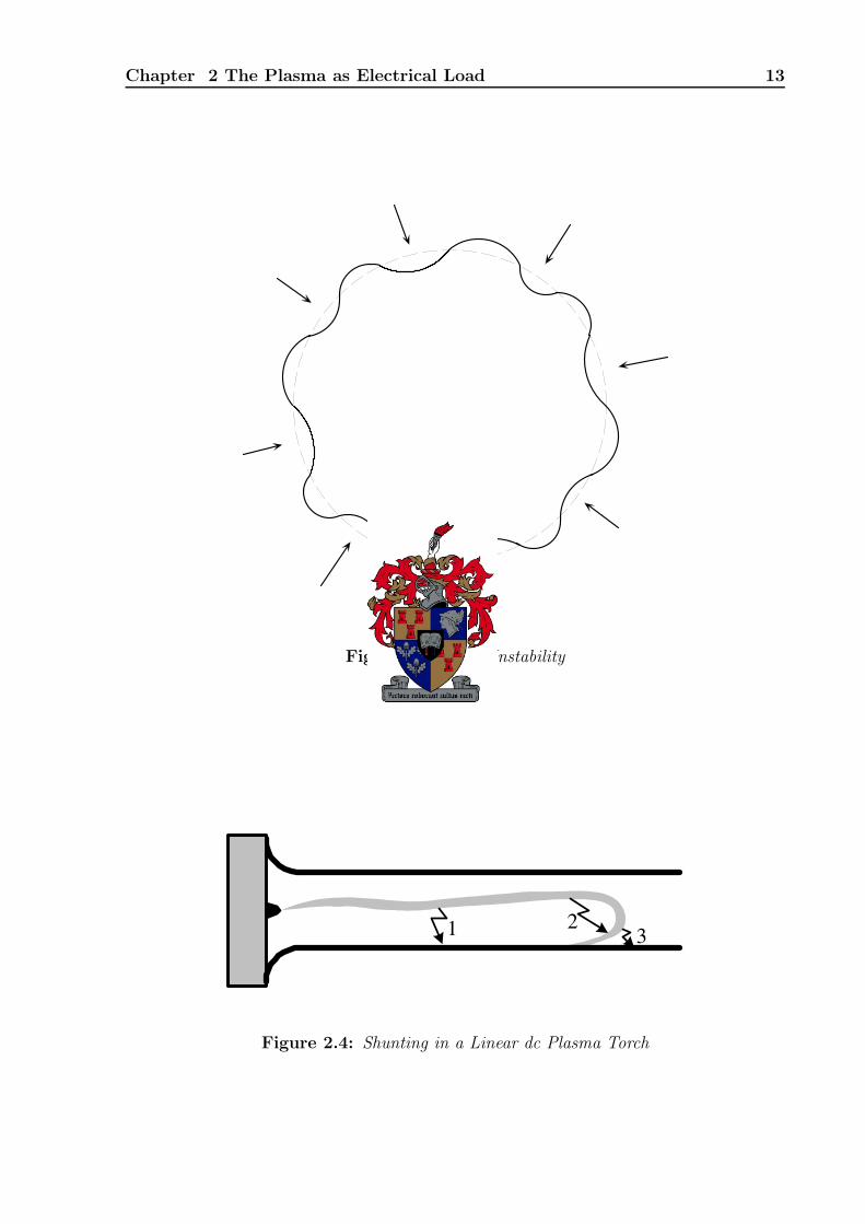
Chapter 2 The Plasma as Electrical Load 13
Figure 2.3: Flute Instability
1 23
Figure 2.4: Shunting in a Linear dc Plasma Torch

Chapter 2 The Plasma as Electrical Load 14
tendency of arcing to occur at the area of maximum ionisation counteracts the ideal
of a moving arc spot, as the small-scale shunting from arc to electrode tend to restrike
close to the still hot and relatively particle-rich area around the previous arc spot.
Near-wall shunting as indicated by 3 in Figure 2.4, in conjunction with the influence
of the gas flow through the torch and the magnetic-field current interaction tends to move
the arc spot toward the nozzle, lengthening the arc. The termination of this process
manifests as large-scale shunting. Large-scale shunting occurs mainly in this form as the
voltage of the elongated arc rises to the boundary value where re-ionisation require less
energy than the established current path. The turbulent gas flow nature at the nozzle
region of the torch enhances the probability of large-scale shunting as the arc is forced
closer to the sidewalls. Large-scale shunting defines the average length of the arc and
hence, the size of the failure area on the electrode [57].
2.2 Behaviour as Electrical Load
The plasma reacts electrically as any static conductor would, in that it conforms to Ohm’s
law and have a resistance proportional to the conductivity and physical dimensions of the
plasma. The simple structure of the plasma arc, in that it has a unidirectional current path
from anode to cathode, results in a very low inductive quality. Although there are small
parasitic capacitive elements between the electrically charged arc and the surrounding,
normally grounded, environment, this influence is swamped by the resistive nature of the
arc.
2.2.1 Variations in Effective Resistance
The resistance of the arc can be given in terms of the average length, area and conductivity
as;
R =le
Aeσe
(2.5)
Due to the stochastic nature of the arc instability mechanisms as described in this chapter
the values of the average length, area and conductivity are time dependent. Although
it would be virtually impossible to model these variations in a qualitative manner the
variations can be assimilated into a statistical model for a given structure and spatial
electrode configuration. This statistical model would, however also be dependent on
the molecular makeup of the ionised gas and the gas flow rate (and gyration, where
applicable). It is clear that such a statistical model can also not effectively predict the
electrical behaviour of a plasma arc under any and all operating conditions even if the
spatial system is fixed.

Chapter 2 The Plasma as Electrical Load 15
The variations in effective resistance can be divided into two main variations, each of
which have distinct effects on the system. If the division is made between the geometric
variations of the electrical arc and the changes in conductivity the following relationships
become clear.
Variation in Arc Dimensions
Variation in the arc length is stochastic in that shunting occurs at random throughout the
arc region. In general the high temperatures in the arc region associated with the plasma,
reduces the ionisation potential of the atoms in the vicinity of the ionised elements. As
the temperature of the non-ionised gas change and the spatial position of the arc (which
being the prominent conductor defines the effective electric field) change the non-ionised
gas is continually subject to a changing ionisation potential. Any non ionised atom will
become ionised as soon as the available electric field is greater than the required ionisation
potential. Therefore it is clear that the variations in length of the system is dependent
on complex physical properties such as the molecular makeup of the non-ionised gas, the
temperature distribution as well as the variations in plasma position, which incidentally
closely mimics the behaviour of a liquid immersed inside another liquid under turbulent
conditions.
The best approximation that can be made would be that the variation in the arc
length would be limited. The mean length of the arc would be a function of the distance
between the anode and cathode. The variation around this mean length would conform to
a normal distribution. The standard deviation would be set by complex variables such as
the gyration of the gas, but in general these elements would limit the average excursion
from the mean arc length. This statement can be clarified by referring to Figure 2.4.
The arc loop length on the output side would be limited as the ionisation potential of the
inter-arc shunting, displayed by 2, is directly proportional to the arc length. The variation
toward a shorter than average arc length will be limited through the low pressure created
in the middle of the conductor space by the gyration of the incoming gas. The electric field
associated with the ionisation of shunting incidence 1 is also lower in that the potential
difference between the grounded body and the cathode is large. Normally the anode is
connected to ground to virtually eliminate the effect of short shunting.
Assuming a constant conductivity and arc area the variation in length would result
in a variation in effective arc resistance, where the resistance is directly proportional to
the arc length. The rapid ionisation of gas molecules, when subject to large enough
ionisation energies, implies that the change from a long arc to a shorter arc will be almost
instantaneous. If short shunting in the form of 1 in Figure 2.4 is minimised it is clear
that the variation from a lower resistance to a higher resistance, as introduced by kink
instabilities, would be bounded in time, while the resistance would drop, with almost step

Chapter 2 The Plasma as Electrical Load 16
like response, to a lower level [57].
Variations in the effective arc area is less pronounced than the sudden changes intro-
duced by shunting. The area of the arc will vary in localised portions of the arc due to
flute and pinch instabilities. These localised portions of diminished arc area will however
move along the arc length with the linear speed of the gas in the arc chamber. If the
linear gas flow rate is high enough the portion of the arc exhibiting a variation of area
will be removed from the arc before the variation has manifested itself enough to have a
noticeable influence on the effective arc resistance. Even in cases where these variations
influence the effective resistance this effect would be slow and gradual compared to the
violent changes introduced by shunting, and therefore negligible.
Variations in Conductivity
According to nuclear physics theory a atom will become ionised when the nett charge
of the atom changes from neutral through either absorption or shedding of a valence
electron. A valence electron will leave the host atom as soon as the electron acquire
enough energy to overcome the force attaching the electron to the host atom, called the
ionisation potential. The total energy of an electron in orbit around an atom can be given
as the sum of the potential and kinetic energy of the electron. The potential energy is
the energy binding the electron to the atom, while the kinetic energy is a measure of the
speed of the electron.
Conservation of energy would dictate that should the electron gain kinetic energy
through some conservative means (i.e. other than a non-elastic collision) the total energy
of the electron must be conserved. As the temperature of a gas increase the valence
electrons in the individual atoms gain kinetic energy and will change to a different state,
with a different potential energy, to apply to the energy conservation principle. The ratio
of electrons in an excited state with energy Eex and at ground state energy Eg can be
given by the Maxwell-Boltzman distribution function for a gas volume.
nex
ng
=Ae
−EexkT
Ae−Eg
kT
= e−(Eex−Eg)
kT (2.6)
Where k denotes the Boltzman constant and T the absolute temperature of the gas. It
is clear that the ratio of the electrons at the higher energy state will increase with an
increase in temperature. The higher energy state also corresponds to a lower ionisation
potential [56].
With an increase in current the movement of ions in the gas also increase implying
an increase in the collision frequency and hence the gas temperature. Although the
ionisation energy can be supplied to an electron in various ways such as photons, the
major contributor to ionisation in a plasma is through collisions. To achieve ionisation

Chapter 2 The Plasma as Electrical Load 17
the colliding electron must have enough kinetic energy to transfer the required energy to
the bonded electron to achieve ionisation without falling back into the newly created hole.
As an increase in current will increase the collision frequency and reduce the average
ionisation energy, ionisation would be achieved more readily at higher currents. A higher
ionisation probability implies an increase in the conductivity of the plasma. Therefore,
in general, the resistance of the plasma would decrease with a increase in current. This
phenomenon is often characterised as the negative resistance property of the plasma. This
term is a misnomer in that the resistance never becomes negative in the pure sense of
the word, implying power delivery, but merely decreases from a positive value to a lower
positive value with an increase in current.
Once the plasma has matured in that the current and resulting ionisation is sufficient
to fill the whole available area, the rate of ionisation stabilises as all the available atoms
has been ionised. Once this occurs the conductivity of the plasma arc settles and the
voltage would again start to increase with an increase in current.
The variation of the plasma conductivity with an increase in current would depend,
once again, on the geometry of the system, the chemical makeup of the gas an the flow
rate of the gas. In general the characteristic V-I curve of a plasma torch is found through
statistical averaging of measured voltage results at different current levels [57].
2.2.2 Generalised Arc Resistance Variation Model
The best approximation of the load characteristics of a plasma would be to combine
the two main influences on the system. The variation in conductivity is much more
predictable through statistical processes and normally a well defined V-I curve would be
available for a given plasma torch. The variation in length and the associated change
in resistance occurs much more randomly, but is confined in magnitude. Therefore the
proposed model is that of a changing resistance in correspondence with the defined V-I
curve with a random bounded voltage source in series with this resistance to mimic the
chaotic changes associated with the variations in length.
2.2.3 Requirements of the Power Converter
In general the arc current is controlled in plasma applications as most of the important
properties such as arc density and temperature are related to the current. The output
power is also controlled in some instances but this can lead to current starvation. Current
starvation occurs when the product of the current and voltage is controlled and the
resistance increases. With the increase in resistance the current decrease while the voltage
might increase resulting in zero variation of the error signal even though the output
resistance has changed substantially. A large enough increase in the resistance could
cause the output current to drop below the critical value needed to heat the gas enough

Chapter 2 The Plasma as Electrical Load 18
to allow continuous ionisation resulting in arc quenching.
The rapid changes in load resistance introduced by the variations in arc length requires
a high bandwidth current source, assuming the output current is controlled. The sudden
decrease in output resistance has the benefit that it would not incur arc quenching, as
the current will tend to increase, but it can however, produce severe over currents in the
driving circuit. No controlled current loop can have sufficient bandwidth to effectively
control such rapid changes in output resistance and therefore the load and source is
decoupled by a high impedance at high frequencies, that is to say by means of an inductor.
Decoupling the source and load with a sufficiently large inductance will have two
benefits. The inductance will limit the current rise slope enough under sudden output
short circuit conditions to enable the control system to limit the source current to within
bounds. The decoupling inductance will also serve as an energy storage device. Should
the resistance of the load increase sharply the energy stored in the decoupling inductance
will be available immediately in the form of a voltage to prevent a sudden change in the
plasma current.

Chapter 3Electric Topology
“. . . I have been convinced by long experience that if I wish to be respectable as a scientific
man it must be by devoting myself to the unremitting pursuit of one or two branches only;
making up by industry what is wanting in force.”
Michael Faraday, 1831
Several converter topologies exist that will satisfy the design goals of this project. A
complete mathematical comparison of the different topologies is an irrational notion,
however the main topological attributes can be compared to facilitate a proper system
selection.
This chapter outlines a study into the topology selection. Keeping with the problem
statement of the project line frequency converters, currently the technology of choice at
medium and high power levels, are analysed to provide a suitable starting point for the
selection. The main drawbacks of these converters are identified and the capability of
high frequency converters to address these areas are discussed. Several high frequency
topologies are investigated and a soft-switched converter is identified and selected for
the primary driving circuit. This converter is analysed in detail. This analysis include
topics such as soft switch facilitation, current waveform determination and switching and
conduction loss characterisation. Finally two rectifier circuits are discussed.
3.1 Line Frequency Technologies
To understand where we are going a thorough understanding of where we come from is
called for. This maxim also holds true for this topology selection.
The most general line frequency supply system used for plasma-like loads is the 12-
pulse controlled rectifier system. This system incorporates two three phase control recti-
fiers driven by two mutually phase shifted three phase voltage supplies. This phase shift
between the supplies is achieved by utilising the inherent 30 phase shift between line and
phase voltages. A single line diagram of such as system is proposed in Figure 3.1.
19

Chapter 3 Electric Topology 20
Υ
∆∆
Figure 3.1: Single Line Diagram of a 12-Pulse Rectifier
In most plasma systems the output current is controlled as the plasma thermal output
power depends on the effective plasma current. The output current is measured and fed
into the control system managing the two rectifier bridges. The nonlinear impedance and
high frequency impedance magnitude variations of the plasma load necessitates the inclu-
sion of a large inductive energy storage tank on the system output. The purpose of this
output inductor is twofold; it supplies the energy impulses needed to reform the plasma
arc after instabilities extinguished the arc, secondly the impedance of the inductance at
control frequencies is larger than the negative resistive nature of the load to present a
controllable positive total impedance.
This arrangement is theoretically expandable to include more phases, e.g. 24 or 36
pulse rectification systems. The inclusion of more phases improves the line regulation
capability and the maximum attainable bandwidth. However expanding the rectifier
increases the cost and size dramatically. The phase shifted three phase supplies are
generated by line frequency transformers which tend to be both bulky and expensive.
Also starring the outputs of several rectifier systems require special attention to both the
control system, to facilitate equal current sharing, and system protection in the event of
a switch element failure.
3.1.1 Output Inductor Considerations
The sizing of the output inductor requires careful attention. The main functions of the
inductor are filtering, energy storage and impedance matching the load to the control
system. However these requirements are mutually exclusive.
The filtering requirements necessitates a large value of inductance. The filtering pur-
pose of the inductor is bidirectional in that it filters both the effect of the input on the
output and vise versa . On the one hand the inductance must ensure that the current will
never be discontinuous under low output power conditions. Any discontinuous current

Chapter 3 Electric Topology 21
behaviour will result in arc quenching as the ions will recombine if the current is removed.
On the other hand the input must be shielded from a sudden short circuit on the output.
The stochastic nature of the plasma load might present an extremely low impedance to
the source for a short period of time. If this short circuit occurs just after rectifier com-
mutation the input supply will be short circuited until the rectifier element commutates
at the current crossing. The resultant current spike might be enough to cause permanent
damage to the supply elements. The filter inductance must be large enough to ensure
that the current rise time is low enough to limit the resultant current spike to manageable
proportions.
The fast reaction time required by the plasma load during arc quenching requires a
well designed filter inductance. The magnitude of the energy needed to re-establish the
arc is rather small as the area in question is saturated with excess ions. However the linear
speed of the airmass containing the ions and the natural recombination characteristic of
the ions quickly diminishes the amount of available ions in the arc region. This implies
that the output inductance must be able to provide the electric field energy immediately
after the arc quenches. Any delay will result in an increase in the energy needed to re-
ionise the gas volume. Practically this translates to an inductance with an extremely
low parasitic capacitance in order for the voltage across the inductor to change polarity
quickly.
During arc initiation the electric field needed to ionise the gas is very high. As soon
as the arc is established the electric field needed to force the ion movement in the form of
current diminishes quickly, resulting in a negative resistance load characteristic. The large
inductance called for by the filter requirements is however unwanted during arc initiation.
The high electric field required for the continual ionisation is absorbed in part by the
voltage reaction of the filter inductance to the increase in current. The newly established
arc requires an electric field and quenches as soon as the field falls below the critical point.
!
"#
Figure 3.2: Preloading the Output Filter Inductor
The requirement of electric field strength at the initiation period is normally satisfied
by preloading the output inductor with a current effectively short circuiting the load, as
shown in Figure 3.2. At the moment of arc initiation the preloaded inductor is switched

Chapter 3 Electric Topology 22
into the circuit where the change in current through the inductance serves to increase the
available field strength instead of diminishing it.
The preloading of the filter inductance requires a well designed initiation circuit. The
requirements of this circuit can be summarised by the following statements. The high
electric field strength required for the initial ionisation must be supplied by an external
source since the main supply output is short circuited. The external voltage source must
produce the electric field in pulses to prevent energy loss into the shorted output of the
plasma supply. The breaker on the output of the plasma supply must be opened at the
moment of arc initiation. These requirements are in general mutually exclusive as there
is uncertainty in the precise moment of initiation. The high frequency source, due to
its pulsed nature, can not sustain the newly formed plasma and when the measurement
circuit detects a current in the load (which requires a conduction path i.e. a plasma)
the breaker must open before the arc quenches due to current starvation. However, the
measurements and the physical response of the breaker introduce a finite time lag to the
system which might prove to be to long. In general plasma initiation is reduced to a luck
of the draw exercise where the high frequency supply is applied across the load and the
breaker is opened at an instant in time in the hope that a conduction path will exist.
3.1.2 Harmonic Pollution
The harmonic content of phase controlled rectifiers are well documented [10, 24]. The
harmonic content of the input line currents of 6-pulse phase control rectifier can be given
as;
i(t) =
∞∑
n=1,5,7,11,...
4
nπIL sin
(nπ
2
)
sin(nπ
3
)
sin (nωt − nα) (3.1)
where IL represents the rectified dc current and α the thyristor delay angle. The inclu-
sion of more phase shifted three phase systems into the rectifier will introduce the same
harmonics on the line currents only phase shifted by the same time lag as the original
line frequency shift. This phase shift cause the destructive interference of some harmon-
ics resulting, for example, in 11th, 13th, 23rd, 25th . . . harmonics in a 12-pulse rectifier
system. The use of a greater amount of pulses, or phase shifted systems, results in higher
frequency harmonics. The harmonic numbers for higher order systems, where the magni-
tude decreases with 1n, can be given as;
n = pk ± 1, k = 0, 1, 2, 3, . . . (3.2)
where p is the pulse number. This implies that the lowest harmonic in a 24-pulse rectifier
would be the 23rd which is easily filtered.
The effect of injected current harmonics in electric distribution systems are well doc-
umented. Injected harmonics can cause voltage resonances, large magnitude negative

Chapter 3 Electric Topology 23
sequence currents and higher than expected rms currents in electrical machines and filter
capacitor banks resulting in premature component failures. To reduce the negative impact
of these harmonic currents, legislation and guidelines have been introduced worldwide in
the form of IEC 1000-3-2 (international), EN 61000-3-2 (European) and IEEE-519. It is
not uncommon for electric utility companies to introduce monetary penalties to customers
exceeding these guidelines.
Harmonic trap filter systems are introduced to large phase controlled rectifier systems
to limit the effect of the harmonics on the distribution system. The design of harmonic
trap filters must be matched to the localised distribution system to prevent unwanted
resonances with nearby power factor correction or energy storage capacitor banks. The
presence of third harmonics, since very few systems present a perfectly balanced load
profile, might also be increased through interaction of the line impedance and the trap
filters at this frequency [10]. The inclusion of trap filters greatly increase the cost and
complexity of a system.
Another aspect of supply pollution is the effect of a sudden load short circuit on the
distribution network. If an extremely low impedance situation arises in the load, due to
impurities in the arc vicinity for example, the primary current will reflect discontinuity of
the load. The interaction of this sudden demand of current with the internal (Thevenin)
impedance of the distribution system results frequently in voltage dips. This is especially
pronounced in rural areas in the vicinity of large arc furnaces.
3.1.3 Isolation Transformer Considerations
Notwithstanding the cost and physical size limitations of line frequency transformers the
interaction of these transformers with the larger system must be taken into consideration.
The isolation transformer serves a dual purpose, firstly to isolate the load from the dis-
tribution system and secondly to introduce any phase shift needed to facilitate 12, 18 or
higher order pulse rectifier systems.
The high prevalence of harmonics in phase controlled rectifier systems have a decre-
mental effect on the isolating transformer operation. The high harmonic content of the
current increases the effective winding current, increasing the transformer copper losses.
The skin effect also makes the increases in losses non-linear, as transformer windings are
designed, in general, for line frequencies.
The power factor of the phase controlled rectifier influence the transformer VA rating.
The phase controlled rectifier exhibits a large shift in effective power factor as the firing
angle shifts to account for load or operating point changes. The phase shift in thyristor
conduction with regards to the voltage waveform ensures that the rectifier power factor
will always exhibit a lagging characteristic with magnitude [10],
pf = 0.955 |cos (α)| (3.3)

Chapter 3 Electric Topology 24
The transformer VA rating should also account for both the maximum attainable
output voltage and current magnitudes. The negative impedance characteristic of the
plasma load requires a very high voltage at low currents and a high current, low voltage
requirement at the working point. The result of this behaviour is that the output power
of the system remains almost constant while the current and voltage magnitudes vary
considerably. The line frequency transformer VA rating must however account for both
the maximum required voltage and the maximum required current due to the internal con-
struction of the transformer. This results in a mismatch between the maximum expected
power requirement of the load and the theoretical power output capacity, expressed in
VA, of the transformer [41].
3.1.4 Control Considerations
The thyristors used in phase controlled rectifier applications are line commutated devices,
implying that after control system commutation, the switch is dependent on the system
current waveforms to commutate into a blocking state. The control system after the initial
switch commutation has no control over the system behaviour until the instant of current
commutation. This implies that the control system of a 6-pulse rectifier, at a frequency
of 50 Hz, can only make an enforceable control decision 300 times a second, a control
frequency of 300 Hz.
From the Nyquist sampling criteria it is known that basic representation of a signal
requires at least twice the sampling frequency than the highest signal frequency compo-
nent. An expansion of this law implies that the maximum bandwidth of a system cannot
exceed half of the maximum control frequency. In other words the 6-pulse rectifier would
not be able to reproduce a controlled output variable with a frequency of more than 150
Hz, and even then it would be of a very low quality.
The fast changing nature of the plasma load do however require a high bandwidth
dynamic response control system. This necessitates the inclusion of a large output filter
inductor, as described in section 3.1.1.
3.1.5 Conclusion
Although the line frequency controlled rectifier system is capable of driving plasma loads,
many modifications must be made to the system to ensure conformity. These modifica-
tions not only increase the the capital cost and complexity of the system but might also
negatively impact on another part of the system’s operational envelope.
In contrast with line frequency technology the newer fast switching technologies ex-
hibit characteristics dramatically different. The recent emergence of switching technology
to the industrial processing fraternity can be attributed to recent advancements in sili-
con switch technologies. The advantages of high frequency systems seems to adress the

Chapter 3 Electric Topology 25
imperfections of line frequency controllable rectifiers.
High frequency converters exhibit a higher attainable control bandwidth, negating
the need for a large output filter inductance. The reduction in filter inductance can also
remove the need for preloading of the inductor as the dynamic response of the system is
high enough to facilitate arc initiation.
The high frequency converter is also in essence an energy converter implying that the
input power requirement is equal to the output power delivery (with a 100 % efficiency).
This also diminishes the VA requirements of the supply system and if needed the line
frequency isolation transformer. In general the constant uncontrolled rectifier of the high
frequency converter also exhibit a better power factor and lower harmonics than the
corresponding phase controlled rectification systems.
In conclusion the search for novel high frequency power conversion systems to replace
and improve the line frequency systems is validated by the inherent shortcomings of these
systems. Also the recent advancements in switch technology enables this expansion of
high frequency techniques into continually larger domains of output power requirements.
3.2 High Frequency Topology Selection
Several isolated power converters exist that will, at first impression, satisfy the design
requirements of voltage isolated current controlled power conversion. However, due to
physical constraints many of these converters are not feasible at high power ratings.
3.2.1 Full-Bridge versus Other Topologies
The investigation and comparison of power electronic topologies must focus on the switch-
ing element and transformer requirements, as these elements are often the limiting factors
in system design. As all the energy converted by the system must pass through the pri-
mary switching elements and the transformer, a comparison of these requirements for
different topologies will yield an acceptable prognosis of the total system behaviour.
The implications on the transformer requirements are by far the most important as-
pect at higher power levels. As transformer magnetic materials can handle finite amounts
of flux excursion two options are available: either larger cores or higher frequencies, both
implying high magnetic losses in the transformer.
To this end the unipole converters, that only utilize one quadrant of the magnetic
material, can be eliminated from the discussion. Forward and Flyback converters only
utilize one quadrant of the magnetic core, in effect using the magnetizing inductance of
the transformer as the energy storage device.
Two converters utilize the full B-H curve of the magnetic material, the half and
full-bridge converters. The half-bridge is however at a disadvantage due to the large

Chapter 3 Electric Topology 26
requirements on the primary capacitances. These capacitances must be large to prevent
bus voltage erosion, a constrictive fact at higher power levels.
The half-bridge converter does have some superior qualities especially in that the
converter exhibits inherent transformer flux balancing. If the transformer primary current
has a dc bias, this dc element will affect the half-bridge voltage. This will cancel the
imbalance in the duty cycles which caused the current error.
A derivative of the half-bridge converter; the partial series resonant converter [35,
46], exhibits soft switching of the active elements as well as complete utilization of the
magnetic material. However, the transformer is not used efficiently. Much time is spent
on facilitating zero voltage switching, while the transformer is idle for a considerable time
through the switching cycle.
At large power ratings the half-bridge converter can not compare with the full-bridge
converter, especially in the transformer and switch ratings and utilization factors. To this
end this project will focus on the full-bridge converter.
3.2.2 ZVS Full-Bridge Topologies
The quest for compact, efficient and reliable power converters force designers to incor-
porate soft switching techniques into their designs. Soft switching has the advantage
that the switch element transitions occur under diminished current and/or voltage biases,
reducing the stresses on the switch and hence the switching losses.
Soft switching converters can be subdivided into Zero Voltage Switching, ZVS, Zero
Current Switching, ZCS, and Zero Current and Zero Voltage Switching, ZCVS. Normally
the soft switching occurs at one of the switch transitions, while the other (either turn-on or
turn-off) still exhibit the ‘normal’ hard switched characteristics. Since it is nearly impossi-
ble to facilitate ZVS conditions on both the turn-on and turn-off transitions some research
focused on ZCVS converters. ZCVS converters sidesteps this boundary by supplying ZVS
conditions at one commutation cycle and ZCS conditions at the other.
ZVS Through Parasitic Element Addition
Although the traditional full-bridge converter is a hard switched converter some modi-
fications can be made to the circuit to facilitate soft switching. If the switching signals
to the full-bridge is derived in a bi-polar manner, by which diagonal switches receive
the same gate signals, some parasitic elements can be added to facilitate soft switching.
These additions normally take on the shape of capacitive and inductive elements used to
store energy during the power transfer cycle. This energy is then utilized to achieve soft
switching at either the turn-on or turn-off transition.
The most common methods of achieving soft switching in a full-bridge converter,
through the addition of extra elements, are the Series Resonant Converter, SRC, the
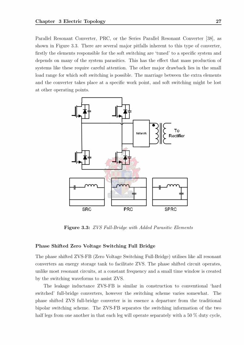
Chapter 3 Electric Topology 27
Parallel Resonant Converter, PRC, or the Series Parallel Resonant Converter [38], as
shown in Figure 3.3. There are several major pitfalls inherent to this type of converter,
firstly the elements responsible for the soft switching are ‘tuned’ to a specific system and
depends on many of the system parasitics. This has the effect that mass production of
systems like these require careful attention. The other major drawback lies in the small
load range for which soft switching is possible. The marriage between the extra elements
and the converter takes place at a specific work point, and soft switching might be lost
at other operating points.
$&%')(*+-, ./, (013254 6798 :
; ')< =>')< ; =>'?<
Figure 3.3: ZVS Full-Bridge with Added Parasitic Elements
Phase Shifted Zero Voltage Switching Full Bridge
The phase shifted ZVS-FB (Zero Voltage Switching Full-Bridge) utilises like all resonant
converters an energy storage tank to facilitate ZVS. The phase shifted circuit operates,
unlike most resonant circuits, at a constant frequency and a small time window is created
by the switching waveforms to assist ZVS.
The leakage inductance ZVS-FB is similar in construction to conventional ‘hard
switched’ full-bridge converters, however the switching scheme varies somewhat. The
phase shifted ZVS full-bridge converter is in essence a departure from the traditional
bipolar switching scheme. The ZVS-FB separates the switching information of the two
half legs from one another in that each leg will operate separately with a 50 % duty cycle,

Chapter 3 Electric Topology 28
with enough dead time between transitions to allow for ZVS transition. One of the half
legs are phase shifted with respect to the other to control the overlap of the two half leg
voltages in time. The effective duty cycle of the converter is controlled by adjusting the
amount of overlap between the two half legs. The phase shift between the two half legs,
leg A and leg B, is shown in Figure 3.4 together with the effective duty cycle (the phase
shift is indicated by θ).
t
t
t
Leg A
Leg B
EffectiveDuty Cycle
Tsθ
Figure 3.4: The Phase Shift Between the Half-Legs of the ZVS-FB
ZVS is achieved through some form of energy storage which provides energy to charge
the switch output capacitance to the bus voltage before the switch is commutated. The
converter operation with transformer leakage inductance storage is described in section
3.3. The phase shifted converter exhibits soft switching in the one of the legs under all
operating conditions although ZVS is lost in the other at very light loads, although a
opportune selection of dead time can ensure ZCS at this point.
Energy storage in the phase shifted converter is usually achieved through the trans-
former leakage reactance. This reactance, inherent to all transformers, provides a natural
storage point. The leakage reactance is however normally to small to ensure ZVS across
a wide load range, but the leakage reactance can be supplemented through the addition
of an external inductance in series with the transformer primary.
Unfortunately any increase in the leakage inductance will also increase the current
commutation time. This has the effect that the effective duty cycle is eroded by the
leakage inductance commutation, especially at higher loads where the inductance stores
more energy than needed. This erosion might be restricted through the use of a saturable
inductance. This inductance will store only as much energy as is needed to facilitate ZVS

Chapter 3 Electric Topology 29
operation and after saturation the inductance is a virtual short circuit and eliminated
from the circuit [8]. The saturable inductance however has a drawback in that saturable
inductors tend to exhibit high hysteresis losses when driven well into saturation.
Other topologies utilize active elements in the secondary rectifier to enhance the
performance of the phase shifted converter. Through adaption of the secondary side
switching information the ZVS range of the converter can be enhanced. This does however
complicate the circuit tremendously. The extra cost and complexity might not be worth
the minimal extension of the ZVS range, especially as the gain is at the lower load range
where the switching losses are manageable [39, 37].
Another energy storage source is the output filter inductance. However, effective
utilization of this energy necessitates a very low transformer leakage reactance [18]. The
transformer leakage inductance is inherent to any transformer construction and minimisa-
tion of this element requires special attention. This can be achieved by utilizing a coaxial
winding transformer, however this type of transformer is not suited for high power appli-
cations.
The loss of ZVS at light loads is of small enough concern that the leakage inductance
assisted ZVS-FB is selected as the topology of choice in this design.
3.3 The Leakage Inductance ZVS Phase Shifted Full-Bridge
Vin
+
1 Coss 3 Coss
4 Coss2 Coss
LL
L
C R
L
Figure 3.5: The Leakage Inductance ZVS-FB with CDR
The leakage inductance phase shifted full-bridge converter utilizes energy storage in
the transformer leakage inductance and a phase shift switching scheme to facilitate ZVS
turn-on. As with any load dependent resonant converter ZVS occurs over a limited range
which can be controlled, or extended albeit at the cost of complexity and reliability. The
main advantage of this topology is that the natural ZVS region occurs at higher loads,

Chapter 3 Electric Topology 30
with the converter lacking the necessary energy to facilitate ZVS at lighter loads, where
the switching losses are lower. This enables the designer to trade unwanted circuit com-
plexities with reasonable switching losses at lower loads to attain the optimum solution.
During the following discussion the assumption was made that the converter operates
with a current doubling rectifier and that the output inductor currents are balanced
and continuous. Under these conditions there will be negligible differences between the
full-bridge primary side operation waveforms of the current doubling and center tapped
rectifiers. A schematic diagram of the leakage inductance ZVS-FB with a current doubling
rectifier is included in Figure 3.5. The Coss capacitance models the parasitic output
capacitance of the silicon switch and LL represents the non-ideal leakage inductance of
the high frequency isolation transformer.
3.3.1 Operational Principle
Each leg is switched at nearly 50% but with an extended dead time. This dead time
creates an environment where the energy stored in the transformer leakage inductance
can be transferred to the switch parasitic capacitances. The phase shift switching scheme
implies that current flow on the primary will be interrupted when a single switch turns off.
As current stored in the leakage inductance cannot be interupted instantly this current will
interact with the circuit comprising of the parasitic output capacitances of the switches
in the commutated leg. The leakage inductance will resonantly transfer energy to the
capacitances. If the dead time of the system is set such that sufficient energy transfer can
take place, the voltage of the switch capacitances will be such that ZVS can be achieved
when the opposing switch in the leg is commutated.
Graphically the converter operation in time can be expressed, albeit with exaggerated
proportions, as in Figure 3.6. The power delivery from primary to the load takes place
during States II and VII. During these transfers energy is stored in the leakage inductance
of the transformer. If, for argument sake, switch 4 is switched off at the end of State II,
refer to Figure 3.5, the energy stored in the leakage inductance will resonantly react with
the output capacitances of switches 3 and 4 as well as the transformer inter winding
capacitance. If the dead time between the gate signals of switches 3 and 4, i.e. the time
allocated to State III, is sufficient the half-leg voltage would ring up to the input voltage
rail, assuming enough energy is stored in the inductor. Once the voltage across switch
4, the half-leg voltage, has reached the input voltage rail the body diode of switch 3 will
clamp the rate of current change and the diode commutation will signal the start of State
IV. As soon as the diode starts conducting switch 3 can be switched on under zero voltage
conditions.
The other conduction states are mirrors of the process described above. The converter
operation in the different states can be described as in Table 3.1. The switching behaviour

Chapter 3 Electric Topology 31
Figure 3.6: Time Waveforms of the ZVS Phase Shifted Full-Bridge

Chapter 3 Electric Topology 32
is however, not perfectly distinct. For example switch 2 can be switched on either well
into State 6 or the commutation of switch 2 could herald the start of State VI depending
on the work point of the converter. However, this table provides a useful guide to the
converter operation. A more in depth study of the converter operation follows in the next
section.
3.4 Converter Operation
The operation of the ZVS full-bridge can be subdivided into 10 different states of which 5
are distinct. Some sub-states do occur, such as discontinuous conduction of the secondary
filter inductors, leakage flux commutation of the secondary diodes etc. The distinct modes
of operation will be discussed, with the other modes being mere mirrors. The behaviour
of the secondary rectifier and load is disregarded in the following discussion, with the
exception where the secondary parameters influence the primary waveforms.
During the discussion and in the ensuing sketches the output diodes are regarded
as ideal, except when stated differently. The parasitic elements of note are the switch
free wheeling diode and output capacitances as well as the referred transformer winding
capacitance.
A Matcad design file outlining the converter operation, at a specific work point, is
included in appendix B and should be consulted in conjunction with this detail analysis.
For clarity sake the operation of the converter is discussed from States II through to VI.
During the ensuing discussion the parameters Vout, Vin, IL1, IL2 and Iout refers to the
output voltage, input bus voltage, the two filter inductor currents and the output current
respectively. For clarity sake ILfis used to denote the current of which ever filter inductor
might be active at that specific time instant.
A summary of the converter states is included in Figure 3.7.
3.4.1 State II, Power Transfer
During State II energy is transferred
leakL
2L
C LR
1L
1D
2D
1
2
3
4
Figure 3.8: ZVS FB State II
from the primary to the load through switches
1 & 4. This phase is initiated at the in-
stant when the primary current magnitude
reach the reflected current stored in the
secondary filter inductor L1. Diode D1 be-
comes negatively biased at the initiation of the power transfer phase when the transformer
secondary windings reflect the applied primary voltage. This voltage commutation is
characterized by an underdamped step response due to the interaction of the transformer
leakage inductance and parasitic diode capacitance. This non ideal behaviour is described

Chapte
r3
Ele
ctr
icTopolo
gy
33
Start Conducting Elements Switched Elements
State 1 Switch 1 on Channel & Body Diode 1 Body Diode 1 off
Channel & Body Diode 4 Body Diode 4 off
State 2 Transformer current reach reflected load current Channel 1 & 4
State 3 Peak Current Reached Channel 1 Switch 4 off
Parasitic Capacitances
State 4 Half-leg voltage reach bus voltage Channel 1 Body Diode 3 on
Channel and Body Diode 3 Switch 3 on
State 5 Fixed frequency operation Channel & Body Diode 3 Switch 1 off
Parasitic Capacitances
State 6 Half-leg voltage reach bus voltage Channel and Body Diode 3 Switch 2 on
or dead time expires Channel and Body Diode 2 Body Diode 2 on
Table 3.1: ZVS-FB State Information
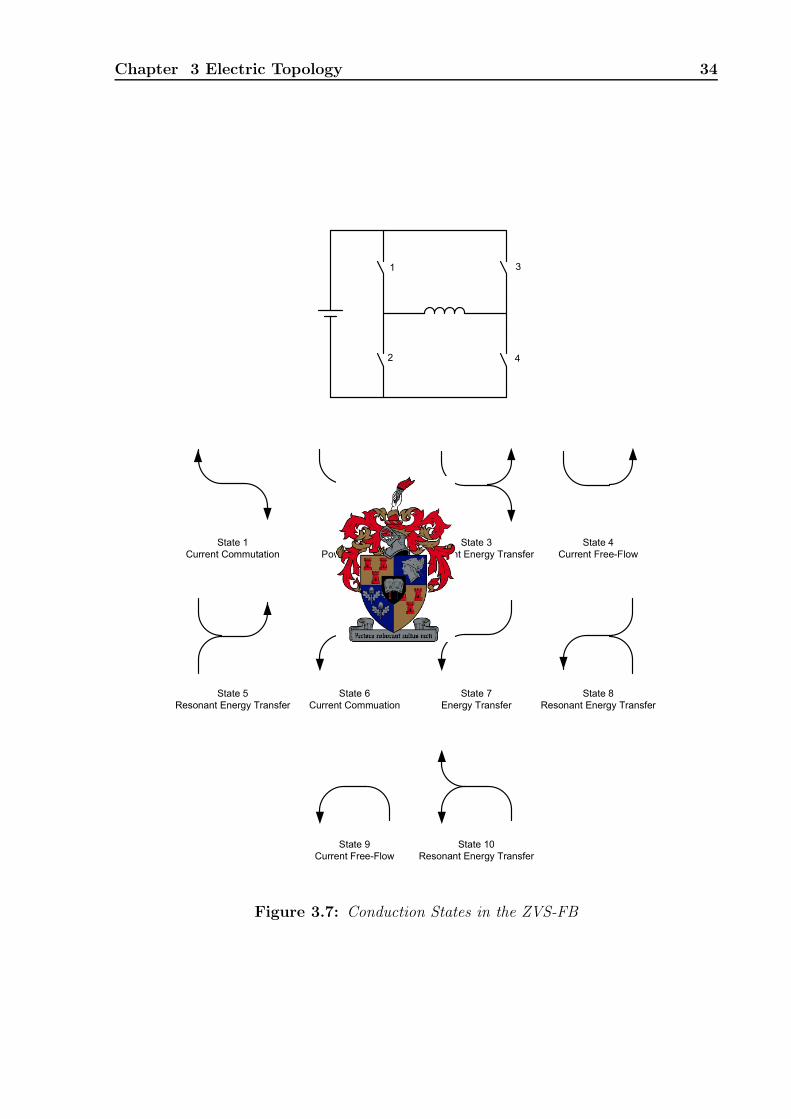
Chapter 3 Electric Topology 34
!
"
#
$
Figure 3.7: Conduction States in the ZVS-FB

Chapter 3 Electric Topology 35
in detail in section 6.3.2
During power transfer the current waveforms resemble those of a conventional full-
bridge converter. The oscillatory response of the secondary voltage damps to the value
predicted by the primary voltage and transformer turns ratio. The primary and secondary
currents increase as a function of the load, filter inductance, primary voltage and the
turns ratio. The effect of the parasitics are negligible except for the reflection of the
underdamped response on the primary current. In general, neglecting the underdamped
output diode reverse recovery transient response, the primary current is given as,
ip(t) =1
aILf
(0) +Vin − aVout
a2Lf + LL
t (3.4)
With the secondary filter inductor currents and output current as,
iout(t) = iL1(t) + iL2(t) (3.5)
iL1(t) = iL1(0) +1aVin − Vout
Lf
t (3.6)
iL2(t) = iL2(0) − Vout
Lf
t (3.7)
The relevant loss mechanisms in state II are the conduction losses. The forward
conduction losses can be modeled as I2R.
Mathematically the conduction loss can be represented as
Wc state2 = (Ip(t))2∆t2(2Rds + Rcu)∆t2 (3.8)
where ∆t2 denotes the time period during which state II is active and Rcu denotes the
copper circuit resistances, inclusive of but not restricted to the transformer winding re-
sistance.
3.4.2 State III, Right Leg Transition
State III, the right leg resonant transi-
leakL
2L
C LR
1L
1D
2D
1
2
3
4
Figure 3.9: ZVS FB State III
tion, is initiated by the turn-off of switch 4.
The magnetic energy stored in the trans-
former and other leakage inductances sus-
tains the full-bridge current direction. Also
note that switch 4 turns off under normal
full-bridge conditions. There is no soft turn-off cycles and the switch is subject to the
switching losses associated with ‘hard switched’ full-bridge converters.
The resonant voltage transition in the right-hand leg is facilitated by the natural
response of the energy stored in the transformer leakage inductance and the combination
of the parasitic output capacitances of switches 2 & 4 and the transformer parasitic
capacitances reflected to the primary.

Chapter 3 Electric Topology 36
The energy stored in the leakage inductance discharges the transformer parasitic ca-
pacitance as well as the output capacitance, Coss, of switch 3 while Coss of switch 4 is
charged. The equivalent small signal model consists of the parallel combination of the
three capacitances in series with the leakage inductance. Mathematically the relation-
ship between the combined capacitor voltage and the inductor current can be given, with
Kirchoff’s law ignoring the dc source in the small signal model;
0 = LL
di(t)
dt+ Ri(t) +
1
C
∫
i(t)dt (3.9)
where LL represents the leakage inductance, R the transformer winding resistance and
C the combination of the switch capacitances and the transformer capacitance. Let the
following terms be defined as:
C = 2Coss + Cxmr (3.10)
ω =1
√LLC
(3.11)
α =R
2LL
(3.12)
Since ω > α for all practical values of R, LL and C the system will be underdamped
resulting in a general solution of the form [26],
I(t) = e(−αt) B1 cos(ωt) + B2 sin(ωt) (3.13)
The current in the primary is at a preset value when the switch commutates, initiating
state III, in other words i(0) is known. At the instant when the bottom right hand switch
is turned off the transformer winding reflects the secondary voltage and the winding ca-
pacitance is charged to virtually the same value as the input bus voltage. Since there is no
voltage present across the leakage inductance at the instant when the switch commutates,didt
(0) will be zero. These values in conjunction with equation 3.13 and the corresponding
differentiated equation results in:
B1 = i(0) = Iset (3.14)
B2 =αB1
ω(3.15)
The voltage of the midpoint of the right-hand leg can be calculated from the current
signal as V (t) = 1C
∫i(t)dt. The resonant voltage can be represented mathematically as;
v(t) = e−αt
αB1 cos(ωt) − ωB1 sin(ωt) + ωB2 cos(ωt) + αB2 sin(ωt)
C (α2 + ω2)
(3.16)

Chapter 3 Electric Topology 37
Typical half-leg voltage and primary current waveforms during this state are included
in figure 3.10. The voltage waveform has been inverted for clarity sake and the ringing is
allowed to continue, although the body diodes of the switches will clamp the voltage to
the rails.
0 5 .10 8 1 .10 7 1.5 .10 7500
0
500
1000
VS3 t( )−
t0 5 .10 8 1 .10 7 1.5 .10 7
20
10
0
10
20
IS3 t( )
t
Figure 3.10: Typical Ringing Voltage and Current Waveforms Associated with State III
Diode D1 starts conducting as soon as the reflected primary transformer current falls
below the current magnitude of L1. Since L1 LL this diode commutation will occur
almost simultaneously with the turn-off of switch 4.
The primary current will decrease in accordance with the energy lost to the voltage
transition, as predicted by:
1
2CV 2
in =1
2LL(I2
3start − I23end) (3.17)
where I3start and I3end denotes the primary current magnitude at the start and end of
State III respectively.
The primary current does not completely follow this prediction when the system is
used with a current doubling rectifier, in that the measured change in current is lower
than predicted. This discrepancy is attributed to the fact that the reflected output filter
inductor is still active in the equivalent circuit of the transient response until the primary
voltage falls below the reflected output voltage. The first part of the transition can be
approximated by including the reflected output inductance in series with the leakage
inductance.
An overview of the operational waveforms is displayed in Figure 3.11. The figure
displays the voltage at the changing transformer primary terminal, the voltage at the
corresponding secondary terminal and the primary current. Knowledge of the voltage at
one terminal on each side of the isolation barrier is sufficient as the other terminals are
clamped to ground through conducting diodes. The primary voltage is also referred to the
secondary for comparison purposes. The change in the primary voltage and the primary
current is clearly distinguishable and seems to conform with the predicted results. The

Chapter 3 Electric Topology 38
−1.5 −1 −0.5 0 0.5 1 1.5−400
−300
−200
−100
0
100
200
300
400
500
Vol
tage
(V) a
nd C
urre
nt (A
)
Time (us)
Primary XFMR Voltage (referred)Secondary XFMR VoltagePrimary Current x 100
Figure 3.11: Operational Waveforms of ZVS-FB used to validate state III
secondary voltage also follows the primary voltage. Closer inspection and measurements
reveal however that the change in the primary current is lower than expected. When
the waveform of Figure 3.11 is investigated closer it can be seen, as displayed in Figure
3.12, that the secondary voltage does not commutate perfectly with the primary. The
resonant change in the primary voltage between the two dotted lines is facilitated by the
output inductance and not the leakage inductance, hence the lower than expected change
in leakage inductance current.
The relevant loss mechanisms during this cycle are the forward conduction losses and
the turn-off losses in switch 4. The conduction loss can be represented by
Wc state3 = (Ip(t))2∆t3(Rds + Rcu)∆t3 (3.18)
The turn-off loss in switch 3 can be calculated, approximatly, by neglecting the effect
of the parasitic output capacitance. The voltage across the switch will have to rise to the
input rail before the current can be redirected from the switch. Assuming the current
remains constant throughout the switching cycle,
W4 off =1
2VinI3starttrise (3.19)
where trise denotes the switch turn-off voltage rise time. This approximation is conser-
vative as not all the energy is dissipated in the switch channel but a considerable portion
of this energy is used to charge the output capacitances to the input rail. The energy

Chapter 3 Electric Topology 39
−40 −30 −20 −10 0 10 20−250
−200
−150
−100
−50
0
50
100
150
200
Vol
tage
(V) a
nd C
urre
nt (A
)
Time (ns)
Primary XFMR Voltage (referred)Secondary XFMR VoltagePrimary Current x 100
Figure 3.12: Waveforms of the Right-Hand Transition During State III of the ZVS-FB
needed to charge the output capacitances can be given by
Wcharge =1
2CV 2
in (3.20)
The switch-off losses will therefore be somewhat smaller than predicted in equation
3.19. However, the maximum value is used in the thermal analysis of the converter.
3.4.3 State IV, Current Free Flow
As soon as the voltage across the switch
leakL
2L
C LR
1L
1D
2D
1
2
3
4
Figure 3.13: ZVS FB State IV
capacitances reaches the bus voltage level,
the resonant energy transfer described in
the previous section is interrupted by the
forward conduction of the body diode of
switch 3. At this instant the primary cur-
rent is free flowing with the voltage across the leakage inductance governed by the con-
duction voltages in the system. Since the conduction resistance in the system is fairly
low, the current in the leakage reactance remains almost constant during the remainder
of the cycle.
After voltage commutation has been achieved switch 3 can be switched-on under
no voltage, and hence no switching losses. After switching the channel of switch 3 also
conducts current in parallel with the body diode, decreasing the forward conduction losses
dramatically.

Chapter 3 Electric Topology 40
The voltage on the transformer terminals are thus clamped to zero on the primary
side. The secondary will reflect this situation, since both the output rectifier diodes are
in conduction.
The primary current during this state can be represented as, assuming all the current
is conducted through the channel of switch 3:
ip(t) = I4starte2Rds+Rcu
LLt
(3.21)
The relevant loss mechanisms during this cycle are the forward conduction losses.
This loss can be approximated as,
Wc state4 = (Ip(t))2∆t4(2Rds + Rcu)∆t4 (3.22)
3.4.4 State V, Left Leg Transition
The left leg transition is initiated by
leakL
2L
C LR
1L
1D
2D
1
2
3
4
Figure 3.14: ZVS FB State V
the switch-off of switch 1. The operational
characteristics of this state is similar to
State III, however the transition will take
much longer.
The energy stored in the leakage reac-
tance will charge both the transformer capacitance and the output capacitance of switch
1, while discharging the output capacitance of switch 2. Mathematically the expressions
are similar to equations 3.9 - 3.16, with the main difference being the initial value of the
stored inductor current. This reduction of the stored energy reduces the peak voltage
attainable by the resonant transition. Hence, the time taken to charge the capacitances
to Vcc is dramatically increased, even though ω remains constant.
It is quite feasible, under low load conditions, that the energy stored in the leakage
inductance is insufficient to ensure ZVS of switch 2. ZVS will not occur when the stored
energy is too low, or mathematically,
LLI25start < CV 2
in (3.23)
A measured waveform of this occurrence is included in Figure 3.15. It is clear that the
switched is switched on under normal, i.e. ‘hard’ conditions and the transition will be
lossy.
However, investigation of equations 3.9 - 3.16 reveal that the resonant voltage and
current is phase shifted by 90. Therefore, the current will be at zero when the voltage
reaches a maximum. Mathcad waveforms of the half-leg voltage and primary current
under incomplete ZVS conditions are included in Figure 3.16. The interdependence of
the current and voltage waveforms are clear.
However, by choosing the dead time equal to a quarter of the resonant frequency the
switch will be switched on under zero current conditions. The required dead time can be

Chapter 3 Electric Topology 41
−2 −1 0 1 2 3 4−50
0
50
100
150
200
250
300
350
400
time (µ s)
Hal
f−Le
g V
olta
ge (V
)
Figure 3.15: Incomplete Voltage Transition During State V
0 5 .10 8 1 .10 7 1.5 .10 7100
0
100
200
300
VS5 t( )−
t0 5 .10 8 1 .10 7 1.5 .10 7
4
2
0
2
4
IS5 t( )
t
Figure 3.16: Incomplete Resonant Transition Half-Leg Voltage and Current Waveforms

Chapter 3 Electric Topology 42
−400 −300 −200 −100 0 100 200 300 400
0
50
100
150
200
250
300
350
time (ns)
Hal
f−Le
g V
olta
ge (V
)
Figure 3.17: State V Transition with Dead Time Chosen at Optimal Value
calculated by
∆t5 =π
2ω(3.24)
Figure 3.17 displays a half leg transition where the energy stored in the leakage induc-
tance is insufficient to produce ZVS. However, the dead time is chosen at the optimum
quarter resonant time period such that ZCS is achieved.
Once again the loss mechanisms during this cycle is the turn-off losses in switch 1 and
the conduction losses in the system. As with State III the losses can be approximated as,
Wc state5 = (Ip(t))2∆t5(Rds + Rcu)∆t5 (3.25)
W1 off =1
2VinI5starttrise (3.26)
3.4.5 State VI, Current Commutation
As soon as the current transition of state V is completed switch 2 is turned on. This
will decrease the on-state resistance as most current will be conducted through the switch
channel.
After switch 2 has been turned on, the voltage across the leakage inductance is
clamped to Vin and the current starts decreasing rapidly, until the current direction re-
verses. At this instant the two diodes of switches 2 and 3 will also commutate. However,

Chapter 3 Electric Topology 43
as the channels of switches 2 and 3 are in conduction in shunt with the diodes, the ensuing
diode recoveries are soft, i.e. nearly lossless.
After current reversal has taken place,
leakL
2L
C LR
1L
1D
2D
1
2
3
4
Figure 3.18: ZVS FB State VI
the current magnitude in the primary will
increase rapidly until the reflected magni-
tude of the current in the filter inductor
L2 is reached. Mathematically the current
during the transition stage can be repre-
sented as,
ip(t) = I6start −Vin
LL
t (3.27)
The secondary voltage of the transformer is also at this point the reflected magnitude
of the primary voltage, effectively driving the leakage reactance current toward the power
conversion cycle.
The relevant loss mechanisms in this state are the forward conduction losses. However,
as ∆t6 is extremely short due to the small leakage inductance, these losses are inherently
low.
Wc state6 = (Ip(t))2∆t6(2Rds + Rcu)∆t6 (3.28)
3.4.6 State VII, Power Transfer
After the primary current reaches the
leakL
2L
C LR
1L
1D
2D
1
2
3
4
Figure 3.19: ZVS FB State VII
reflected magnitude of the filter inductance
L2 the mirror of the power transfer cycle
of state II starts. At this instant in time
the secondary diode D2 commutates, again
with the undamped response described ear-
lier.
The current in the system will now again be governed by the bus voltage, load, filter
inductances and the transformer turns ratio. After the initiation of state VII the system
operates as a mirror of the states described earlier. However, it is important to note that
the left hand leg will in this instance also be commutated last. This implies that under
light loads the right hand leg will always experience ZVS while the same cannot be said
for the left hand leg.
3.4.7 Model Validation
The time analysis of the converter, as described in the preceding sections, was imple-
mented in a Mathcad design file, included in appendix B. Figures 3.20 and 3.21 represents
the measured and calculated primary current waveforms. Although there are slight dis-

Chapter 3 Electric Topology 44
crepancies, especially due to explicit knowledge of the converter work point, the similarity
of the two waveforms are evident.
−10 −8 −6 −4 −2 0 2 4 6 8 10−15
−10
−5
0
5
10
15
time (µ s)
Prim
ary
Cur
rent
(A)
Figure 3.20: Measured Primary Current
3.5 Secondary Rectifiers
Several methods of rectification exists, each with unique advantages. The analysis of each
of the rectifier circuits is further complicated in that the interaction of the rectifier with
the rest of the circuits often distorts or changes the operating conditions of another part
of the circuit. Although an in depth study of the effect of each of the circuits would be
ideal, this study will only focus on some of the more notable aspects of this effect.
The ideal rectifier will convert the high frequency ac signal form the transformer
into dc with negligible losses and conducted EMI. The complexity of the rectification
circuit should also be as low as possible. To this end the use of synchronous rectification
techniques are excluded from the study as these techniques find their niche more in high
current low voltage applications where the forward voltage drop of rectifier diodes becomes
unacceptable. This study will only compare the center tapped and current doubling
rectifier. A complete comparison of the requirements and losses of the rectifier magnetic
components is included in section 4.2.
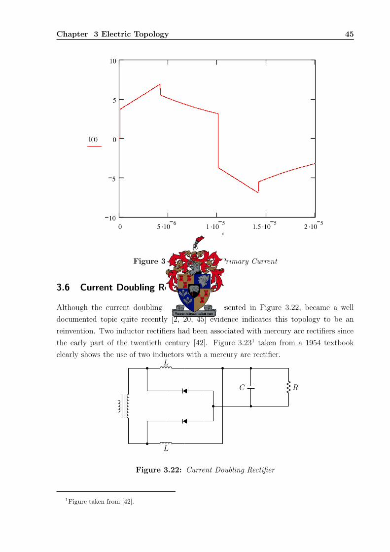
Chapter 3 Electric Topology 45
0 5 .10 6 1 .10 5 1.5 .10 5 2 .10 510
5
0
5
10
I t( )
t
Figure 3.21: Calculated Primary Current
3.6 Current Doubling Rectifier
Although the current doubling rectifier, as represented in Figure 3.22, became a well
documented topic quite recently [2, 20, 45] evidence indicates this topology to be an
reinvention. Two inductor rectifiers had been associated with mercury arc rectifiers since
the early part of the twentieth century [42]. Figure 3.231 taken from a 1954 textbook
clearly shows the use of two inductors with a mercury arc rectifier.L
C R
L
Figure 3.22: Current Doubling Rectifier
1Figure taken from [42].

Chapter 3 Electric Topology 46
Figure 3.23: Current Doubler: Early Twentieth Century
0 5 10 15 20 25 30 35 40 45 500
1
2
3
4
5
6
7
8
9
10
Time (µ s)
Cur
rent
(A)
Inductor 1 CurrentInductor 2 CurrentOutput Current
Figure 3.24: Current Waveforms of the Doubling Rectifier Under CCM

Chapter 3 Electric Topology 47
The main advantage of the two inductor rectifier lies in the current doubling effect,
resulting in the analogous term current doubler. With reference to Figure 3.24 only half
of the total output current, Iout flows through the secondary of the transformer during the
conduction interval. The remainder of the current is supplied from the energy stored in
the free-flowing inductor. This doubling effect has the benefit of reducing the conduction
losses in the transformer secondary.
3.6.1 Operation
Several states of operation can be identified in the CDR (current doubling rectifier).
These different states describe the behaviour of the secondary inductor currents. As with
all rectifiers the secondary current is a reflection of the primary current. However, the
CDR inductor currents will be unbalanced if the primary current has a dc bias. Since a
design goal of the control system is to remove any dc-bias form the primary current, an
assumption can be made that the secondary inductor currents are balanced.
The operating region of the CDR, with symmetrical control on the primary, can
be divided into two main categories, continuous and discontinuous conduction, as with
any converter. Under continuous conduction the inductor currents are positive and the
transformer current is equal to the inductor current during the rising slope. This implies
that there is no circulating current in the system.
Operation under DCM can be subdivided into four different states [45], which occurs
at different regions of the operating envelope. Figure 3.25 gives an indication of the
current waveform in one of the inductors for each of the states. Under very low output
power situations the output inductor current direction might even reverse. By defining a
constant describing the impedance ratio between the output inductors and the load, the
boundaries of the different states can be defined as in Figure 3.26
ωLout
RL
→ k =2Lout
TsRL
(3.29)
with D describing the duty cycle of the converter.
The two inductors in the output path provides current doubling but the effect on the
output voltage is that the output voltage of the system is halved. This implies that the
secondary of the transformer will need double the turns of the center tapped rectifier.
The rectifying diodes in turn must also be rated for this higher voltage. Investigation of
Figure 3.22 reveals that if a diode is conducting the other diode will have to block the
full voltage available on the transformer secondary. The output diodes must be rated to
withstand at least twice the desired output voltage and half the output current.
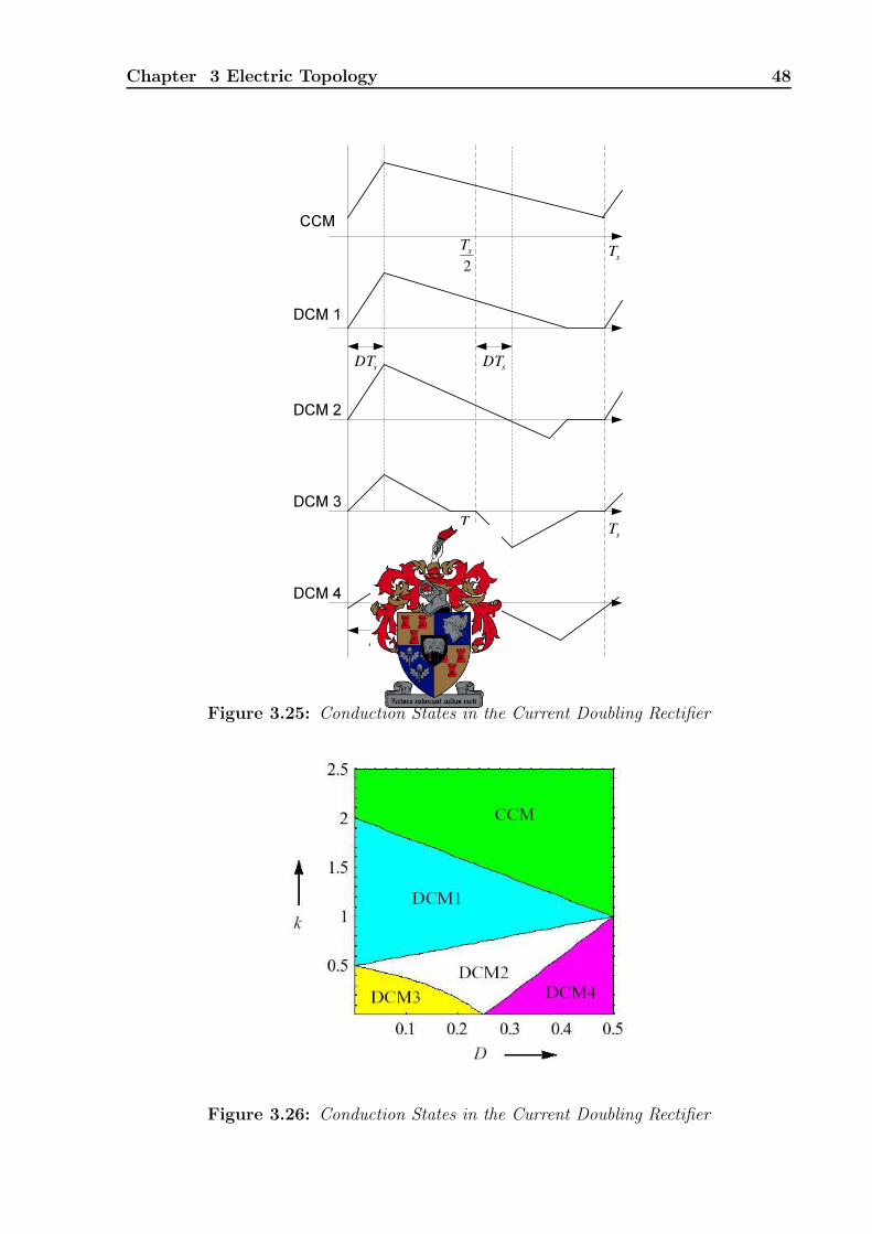
Chapter 3 Electric Topology 48
CCM
D CM 1
D CM 2
D CM 3
D CM 4
2sT
sT
sDTsDT
sT2
sT
sTD′
Figure 3.25: Conduction States in the Current Doubling Rectifier
Figure 3.26: Conduction States in the Current Doubling Rectifier

Chapter 3 Electric Topology 49
L
C R
Figure 3.27: Center Tapped Rectifier
3.6.2 Center Tapped Rectifier
The center tapped rectifier operates as a full-wave rectifier where the rectifier diode re-
quirement has been reduced from four to two through the addition of a center tapped
voltage. This center tapped voltage is normally also taken as the secondary reference
voltage.
The current operation of the center tapped rectifier is such that the total output
current is carried through the output inductor, at all times, and through each rectifier
diode, in turn. The output voltage is the rectified time average of the output voltage of
each of the transformer secondary windings. This implies that the full required output
voltage must be available at each of the secondary windings. Since output diodes are
connected between the transformer and the output filter inductor and the voltages on the
two secondary windings are mirror images of one another the voltage blocking requirement
of the diodes are at least twice the required output voltage.
The secondary of the transformer will be similar to the secondary of the current
doubling rectifier, with the same number of turns on both transformers. The center
tapped rectifier transformer is however a little more complicated in that it incorporates
an extra termination midway through the winding. The transformer secondary current
is also higher in the center tapped configuration as the complete output current flows
through the winding for half of the on time of the system. Therefore the losses in the
transformer secondary will be higher than in the current doubling rectifier.

Chapter 4System Design
“I keep the subject of my inquiry constantly before me, and wait till the first dawning
opens gradually, by little and little, into a full and clear light”
Isaac Newton
An aim of this thesis project is to design and test a 3 kW prototype converter for plasma
applications. However, the ultimate aim of the complete project is to design a high
frequency switch mode supply for applications in a mineral processing plant at power
levels exceeding 500 kW. To this end novel controllers, topologies and control algorithms
are ignored. The 3 kW unit is also designed such that two ore more converters can be
operated in parallel to facilitate operation at higher power levels.
Therefore this 3 kW prototype design functions as a platform to test the function-
ality of the proposed full-scale system. The main advantage of the prototype lies in the
relatively inexpensive component cost, which in turn yield greater freedom for experimen-
tation. The 3 kW prototype will be operated in conjunction with a Russian water vapor
plasma cutter.
The output characteristics of the prototype is summarised in table 4.1. The input
power is limited to ensure operation from a normal residential power outlet. Maximum
power delivery is limited by incorporating power limits on both the rectifier, at a higher
level, and the full bridge converter.
The unit can be described as a ZVS full-bridge incorporating a current doubler high
frequency rectifier. The system is supplied by a PFC boost rectifier. The design criteria
of each of these elements will be developed during the following sections. A block diagram
overview of the system is included in Figure 4.1
4.1 Full Bridge
The design of the full bridge can be subdivided into dimensioning, ZVS implementation
and the control system. The control system with the exclusion of the slope compensation
50

Chapte
r4
Syste
mD
esig
n51
!"
#
!
$%
""
!
&'(
)
Fig
ure
4.1
:Block
Dia
gram
ofth
eC
om
plete
System

Chapter 4 System Design 52
Output Voltage 0-400 V
Output Current 0-8 A
Maximum input power 3000 W
Efficiency 90 %
Power Factor > 0.9
Table 4.1: Design Parameters for 3 kW System
parameter will be discussed in chapter 5.
4.1.1 Switch Element Dimensioning
The dimensioning of the converter elements is a rather easily accomplished feat once the
converter operating envelope has been determined.
The primary switches are voltage rated to withstand the primary bus voltage plus
a derating factor (to allow for switching transients and lower component stresses). The
switch current is proportional to the output current and the transformer turns ratio. This
current is also derated to allow for lower switch stresses.
Since the energy storage requirement of the transformer leakage inductance is directly
proportional to the magnitude of the switch and transformer output capacitances, these
parameters should be minimised as much as possible.
The body diode of the switch also deserves attention as this element is indispensable
in the converter operation. The important diode parameter is the diode reverse recovery
charge and the corresponding reverse recovery time. Since the converter is operating in an
extreme environment where the output can be short circuited, the resulting effective duty
cycle can be very small. With reference to section 3.4 the following discussion sketches
this phenomenon.
During state V the current is flowing through both the body diode and the channel of
the lower switch. The instant the current commutates the current rise time is extremely
high due to the short circuited output and the corresponding on-time (until the current
determined by the peak current control system - refer to chapter 5 - is reached) can be very
short, in the region of 400 - 800 ns. This might imply that the switch is turned off, with the
corresponding increase in reverse voltage, before all the minority carriers in the channel
diode has recombined. This will result in a catastrophic failure as the channel diode
will simply start conducting in the opposite direction and eventually breakthrough and
present a short circuit across the bus, in conjunction with the top switch [1]. Fortunately
the transformer leakage reactance serve to restrict the magnitude of this current rise time,
thus minimising the risk of this failure.

Chapter 4 System Design 53
The risk of this failure mode is minimised through selection of FET switches with
fast recovery free-flow diodes. International Rectifier, among others, market a MosFet
range named FREDFET, Fast Recovery Diode Field Effect Transistor. The alternative
to FREDFET technology lies in the selection of IGBT’s. IGBT’s typically are more robust
and unlike MosFet’s do not have an inherent parasitic anti-parallel diode. This important
characteristic implies that the free-flow diodes in the system can be comprised of discrete
hyper-fast diodes which will improve system reliability. IGBT’s also exhibit lower output
capacitances than MosFets thus improving the feasible ZVS load range. However, the
switching characteristics of MosFet’s are superior to those of IGBT’s.
4.1.2 ZVS Implementation
With reference to section 3.4, there are two instants during each power conversion cycle
where ZVS is facilitated. These resonant intervals are characterised by the transfer of
energy from the leakage inductance to the combined output capacitance of the switches
and the transformer. For convenience the characteristic equations describing this energy
transfer are repeated here;
C = 2Coss + Cxmr (4.1)
ω =1
√LC
(4.2)
α =R2
2L(4.3)
i(t) = I0 · e−αt cos(ωt) (4.4)
v(t) =I0e
−αt
C(α2 + ω2)ω sin(ωt) − α cos(ωt) (4.5)
From the conservation of energy, neglecting the intrinsic wire and ESR resistances;
WL =1
2LI2
WC =1
2CV 2
WL = WC (4.6)
Combining this relationship and with two resonant cycles per conversion cycle the min-
imum energy stored in the inductor must be twice the requirement of the capacitances.
This results in a trade-off between the amount of leakage inductance and the primary
current magnitude at which ZVS will be achieved;
Imin =
√
2C
LV (4.7)
The first of these resonant cycles occurs directly after the power conversion cycle,
implying that the current in the storage inductor is at its maximum. The voltage rise

Chapter 4 System Design 54
time of the capacitors can be represented by equation 4.5. Realising that, in general,
ω α the voltage peak can be given as;
Vp =ωI0
C(α2 + ω2) Vcc (4.8)
Clearly the time needed to facilitate ZVS is not related to the natural frequency of
the system, ω, but to the voltage rise time, determined by the circuit parameters and
the current stored in the inductance. With, again, the assumptions that ω α and
sin−1(δ) ≈ δ for small values of δ the time needed to reach the bus voltage Vcc can be
given as;
tr1 ≈VccC(ω2 + α2)
I0ω2<
π
2ω(4.9)
Since the conduction losses are minimised considerably by switching the switch in parallel
with the body diode, it is imperative to minimise the time allowed for resonant energy
transfer.
At the start of the second resonant interval the current in the inductor, neglecting
conduction losses, will have decreased to:
I1 =
√
I20 −
C
LV 2
cc (4.10)
which under low current conditions might not be sufficient to ensure ZVS. However, at
the end of the resonant interval the converter is set for the power conversion state as the
transformer current has commutated. Therefore it is feasible to allow as much time as
possible to facilitate ZVS in this state. Investigation of the current reveals, importantly,
that at the instant t = π2ω
the current commutates and has negligible magnitude. Choosing
this instant for switch commutation will result in ZCS with the added benefit of a reduced
voltage across the switch. The beauty of this arrangement lies in the invariability of ω on
the operating point, since ω depends purely on the converter elements.
4.1.3 Slope Compensation
The instability of peak current mode controlled systems (refer to chapter 5) at duty
cycles beyond 50 % are well documented and understood. A theoretical analysis of this
instability mode is given in section 5.2.1.
The current doubling rectifier however exhibits an output inductor current frequency
proportional to the switching frequency. The resultant of which implies that the output
inductor current duty cycle (rise-time vs time proportion) can never exceed 50 %. The-
oretically it should therefore be possible to operate the system without the addition of
slope compensation.

Chapter 4 System Design 55
However, the internal switch current loop in the system is critical to the total converter
operation and any disturbance in this loop will cause large scale system instabilities. The
addition of slope compensation reduces the overall loop gain of this internal current loop,
increasing the noise insensitivity of the overall control system. Although every effort has
been made in the system design and layout to minimise noise, the localised noise in the
inner current loop might prove to be unacceptable. To this end, provision has been made
for the introduction of slope compensation into the system.
Slope compensation addition to the sensed switch current information is achieved
through the addition of a portion of the timing clock waveforms. A variable voltage ramp
can be added to the sensed waveform through the addition of a capacitive network to the
current sensing pin of the UC3875 phase shifted controller.
Although the system is designed to theoretically operate without the addition of slope
compensation, compensation will be added to ensure the stability of the inner control loop.
4.2 Output Inductance
The appropriate choice of output filter inductance is crucial to the operation of the holistic
system [31]. Several system variables such as the primary current shape, output current
ripple and the DCM (discontinuous conduction mode) boundary are defined (albeit in
part) by the filter inductance. In practice the perfect value to satisfy all needs proves to
be illusive but a study of the output current ripple and inductor losses yields a perfectly
acceptable value.
4.2.1 Output Current Ripple
The effect of the output current ripple is somewhat more pronounced in this system
than in most other power supplies. The low capacitive storage capability of the output
minimizes the usual second order filter characteristic introduced by the capacitor. This
coupled with the emphasis on the output current as controlled parameter, inflates the
significance of this variable somewhat.
The output current ripple depends purely on the switching frequency, the inductance
of the output filter and the voltages on both sides of the isolation transformer. This
dependence is mathematically derived for the CTR (Center Tapped Rectifier) in section
A.4.1 and can be expressed as:
di =Vout(Vin − Vout)
2LVinfs
(4.11)
The relationship between the output voltage and the ripple is shown in Figure 4.2 for
several inductor values, with a constant input voltage of 400 V.

Chapter 4 System Design 56
0 50 100 150 200 250 3000
0.5
1
1.5
2
2.5
3
3.5
Output Voltage (V)
Pea
k−P
eak
Rip
ple
Cur
rent
(A)
300uH400uH500uH600uH
Figure 4.2: Output Current Ripple vs Output Voltage (Vin = 400V )
Although a very small ripple value is desirable, the physical realization of the inductor
limits the attainable ripple value. The attainable inductance with a certain magnetic core
under dc-current bias conditions is inhibited by the Li2 relationship, as shown in section
A.5.1. Manipulation of equation A.45 reveal the dependency of the flux density upon the
material, core geometry and the Li2 factor, as shown;
B =
√
Li2µ0µr
Aele(4.12)
With reference to Figure 4.3 the dBdH
slope changes as the magnetic material approach
saturation. Realisation that in general µ ∝ dBdH
and L ∝ µ shows that a change in the
magnetisation slope will affect the inductance. The effect of this relationship is that the
inductance of an inductor will decrease with an increase in dc-bias. Physical realization of
an inductor operating under dc-bias should take this into consideration, through proper
core selection; where the flux density under dc-bias is low enough to permit a reasonable
excursion about the work point. The above criteria are met by selecting a corner density
value, Bc, at 80 % of Bsat and ensuring that the flux density remains below this value dur-
ing normal operation. These requirements and the definition of a core selection constant,
κc are summarized as;
L(idc + .5∆i)2 ≤ (.8Bsat)2Aele
µ0µr
≡ κc (4.13)

Chapter 4 System Design 57
H
B
Figure 4.3: Typical B-H Curve for a Ferrite
In order to design an optimized inductor the precise ripple current of the output
inductor is needed. Keeping with the goals of this text both the CTR and the CDR,
Current Doubler Rectifier, will be studied.
Center Tap Rectifier
sT
2sT
2)1( sT
d+2sT
d time
Cur
rent
mini
TsoutI )(outi∆5.0
Figure 4.4: Output Current Waveforms of the Center Tap Rectifier
With reference to section A.4.1, and Figure 4.4 the output current of the CTR can
be described as:
iout(t) =
imin + Vin−Vout
L(0 ≤ t < dTs
2
imin + (Vin−Vout)d2Lfs
− Vout
L(t − dTs
2) (dTs
2≤ t < Ts
2)
(4.14)
The assumption that the output voltage remains constant during the duration of the
switching cycle yields a linear output current as shown in equation 4.14 which compares
well to the more accurate second order approximation. This linear relationship implies
that the average output value is found by calculating one half of the excursion from the

Chapter 4 System Design 58
minimum value or,(
iout(t))
Ts
= imin +(Vin − Vout)Vout
4VinLfs
(4.15)
the excursion about the average work point can be given as;
0.5∆iout =(
iout(t))
Ts
− imin =(Vin − Vout)Vout
4VinLfs
(4.16)
which corresponds well with equation 4.11.
Differentiation of equation 4.16 with respect to Vout and finding d∆iout
dVout= 0 reveals
that the ripple would reach a maximum at Vout = 0.5Vin. This relationship is also evident
in Figure 4.2. Finding the required inductance value corresponding to a desired output
ripple, with ∆I defined as the desired peak-peak ripple percentage of I0, the maximum
output current;
L =Vin
8∆II0fs
(4.17)
Substitution into equation 4.13 gives the core selection constant,
κcent =VinI0
8∆Ifs
(1 + 0.5∆I)2 (4.18)
Current Doubler Rectifier
sT
2sT
2)1( sT
d+2sT
d time
Cur
rent
mini
sToutI )(
outi∆5.0
1Li
2LisTLI )(
minLiLi∆5.0
Figure 4.5: Output Current Waveforms of the Current Doubling Rectifier
With reference to section A.4.1 and Figure 4.5 the inductor and output currents can
be described as;
iL1(t) =
iLmin+ 2Vin−Vout
Lt (0 ≤ t < dTs
2)
iLmin+ (2Vin−Vout)d
2Lfs− Vout
L(t − dTs
2) (dTs
2≤ t < Ts
2)
(4.19)

Chapter 4 System Design 59
iout(t) =
2iLmin+ Vout
2Lfs+ 2Vin−Vout
Lt (0 ≤ t < d ts
2)
2iLmin+ Vout(Vin−Vout)d
Lfs− 2Vout
L(t − dTs
2) (dTs
2≤ t < Ts
2)
2iLmin+ Vout
2Lfs+ 2Vin−Vout
L(t − Ts
2) (Ts
2≤ t < (1 + d) ts
2)
2iLmin+ Vout(Vin−Vout)d
Lfs− 2Vout
L(t − Ts
2) (Ts
2(1 + d) ≤ t < Ts)
(4.20)
The average output current is shown, in the same manner as the CTR output current, to
be:
(iout(t)
)
Ts
= imin +(Vin − Vout)Vout
2VinLfs
(4.21)
The minimum value of the output current is found with reference to Figure 4.5 as:
imin = 2iLmin+
Vout
2Lfs
(4.22)
which reveals;
0.5∆Iout =(Vin − Vout)Vout
2VinLfs
(4.23)
incidentally double the ripple found in equation 4.16 with the same inductance value.
Rewritten for the required inductance value at maximum ripple, i.e. Vout = 0.5Vin,
L =Vin
4∆II0fs
(4.24)
Optimized inductor design in the CDR requires however, the ripple component in
each of the output inductors.
(IL(t))Ts= iLmin
+(2Vin − Vout)Vout
4VinLfs
(4.25)
0.5∆iL =(2Vin − Vout)Vout
4VinLfs
(4.26)
Manipulation of equations 4.23 and 4.26 reveal the relationship between the output and
inductor current ripple.
∆iL =2Vin − Vout
Vin − Vout
· 0.5∆iout (4.27)
Resulting in a inductor ripple of 1.5 times the output ripple at the point, Vout = 12Vin, of
maximum inductor current ripple.
Differentiation of equation 4.26 with respect to Vout reveals that the maximum ripple
will occur at Vin = Vout or a 100 % duty cycle with the assumed 1:2 turns ratio. Giving
a worst case ripple value of,
∆iL =Vin
4Lfs
(4.28)

Chapter 4 System Design 60
The core selection constant for the CDR can be calculated as:
κdoubl = L(
0.5I0 +Vin
4Lfs
)2
(4.29)
Substitution of equation 4.24 in 4.29 yield the core selection constant in terms of the
desired output ripple current.
κdoubl =VinI0
4∆Ifs
(∆I + 0.5)2 (4.30)
The core size requirements of both the CTR and CDR is shown in Figure 4.6 against
the desired output ripple. From this illustration it is clear that the core size requirement
of the CDR cannot realistically be taken as half of the CTR’s; at a realistic ripple value
of 15 % the CDR requires 73 % the core size of the corresponding CTR inductor.
5 10 15 20 25 30 350.02
0.04
0.06
0.08
0.1
0.12
0.14
0.16
Ouput Current Ripple (% of Imax)
Cor
e S
elec
tion
Con
stan
t
CTR RequiremntCDR Requirment
Figure 4.6: κ vs ∆I0 for CDR and CTR
4.2.2 Inductor Losses
Loss Mechanisms
Inductor losses are in general an extremely illusive comparative parameter due to the
many degrees of freedom influencing the losses. The losses in the inductor can be divided
into magnetic and Ohmic losses, both of which depend on a number of weakly-correlated
parameters. Throughout this section the inductor-losses of both the CDR and CTR
will be investigated with the same design parameters. The values, except when stated
differently, used during this chapter are summarised in Table 4.2

Chapter 4 System Design 61
CTR CDR
Inductor 500 µH 1 mH
Core E 56/24/19 ETD 49
Material 3C90 3C90
Airgap 2.6 mm 1.8 mm
Turns 55 turns 82 turns
Wire Information 0.5 mm 9 strands Litz 0.45 mm 9 strands Litz
Conductor Length 6.16 m 6.97 m
Winding Resistance 10 mΩ 26 mΩ
Current Ripple 20 % 20 %
κ 77 × 10−3 34 × 10−3
Window Fit 80 % 79 %
Ripple Frequency 100 kHz 50 kHz
Table 4.2: Default Rectifier Design Values
Magnetic losses
Magnetic losses result from a number of sources of which the most pronounced are hys-
teresis and eddy current losses. The existence of hysteresis loss is evident in observation
of the magnetic materials B-H curve. Mathematically the existence can be proved,
W =
∫
Ts
v(t)i(t)dt
=
∫
Ts
(
nAc
dB(t)
dt
)(H(t)len
)
dt
= (Aele)
∫
Ts
HdB (4.31)
where Aele is the volume of the core.
Eddy currents occur in a magnetic core since magnetic materials are in general good
electrical conductors. According to Lenz’s law, currents will flow in a medium in a manner
to oppose the time varying flux, φ(t). These currents result in I2R losses in the resistance
of the magnetic medium. The induced voltage in the core is proportional to the derivative
of the flux through the core. If the resistive property of the core is independent of
frequency, the magnitude of the currents will increase linearly with f and hence the losses
with f 2.
The exact losses in a magnetic core are difficult to calculate analytically, but the
following relationships yield an acceptable value of the sum of the discussed losses;
Pcore = Kf (∆B)βAele (4.32)

Chapter 4 System Design 62
where β is a constant associated with the specific material and Kf can be approximated
with a fourth order polynomial of f .
If the inductors are optimally designed the flux swing due to the ripple current will be
equal in each case. This will transpire as the airgap will be chosen to limit the maximum
flux at maximum current to the same value. Therefore from equation 4.32 the loss in
each of the inductors can be found, where it is clear that the loss in the CDR should be
a quarter of the CTR loss per m3, given that the polynomial Kf is approximated by cf 2.
With the size differences between the cores, as discussed in table 4.2 the core loss in the
CTR will be three times larger than the CDR.
Comparison between the magnetic elements requires that the same magnetic material
is used for both inductors. Material 3C90 from FERROXCUBE has been chosen for the
comparative studies.
Copper Loss
The conductor losses depend on a number of factors; to facilitate the comparison the
following assumptions take precedence.
• The skin effect will be taken into account.
• The simple structure of the inductor mitigates the proximity effect, which will be
ignored.
• The window fill area will be optimised in the design of both inductors, i.e. the wire
size will be chosen to fill the allowable window area.
The skin effect cause the majority of the current to flow along the outer surfaces
of the conductor. The skin effect can be modelled by shrinking the effective area of the
conductor as the frequency increase. The penetration depth of the high frequency current,
δ is given by:
δ =
√ρ
πµ0µrf(4.33)
The inductor currents of both the CTR and CDR as shown in figures 4.4 and 4.5 can
be modelled as a triangular current shape superimposed on a dc value. Fourier series
approximation of the ac part of the waveforms yields a magnitude at harmonic k:
iac(k) =∆IL
π2k2d(1 − d)
√
1 − cos2(dπk) (4.34)
with ∆IL defined as the zero to peak inductor ripple and d represents the duty cycle.
With reference to equation 4.33 the effective conductor area under skin effect con-
ditions can be represented as 2rδπ − πδ2, where r is the true conductor diameter. The
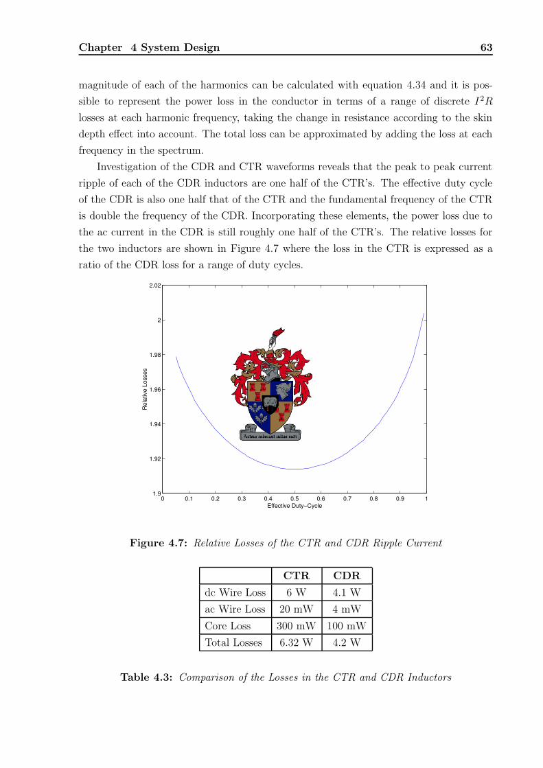
Chapter 4 System Design 63
magnitude of each of the harmonics can be calculated with equation 4.34 and it is pos-
sible to represent the power loss in the conductor in terms of a range of discrete I 2R
losses at each harmonic frequency, taking the change in resistance according to the skin
depth effect into account. The total loss can be approximated by adding the loss at each
frequency in the spectrum.
Investigation of the CDR and CTR waveforms reveals that the peak to peak current
ripple of each of the CDR inductors are one half of the CTR’s. The effective duty cycle
of the CDR is also one half that of the CTR and the fundamental frequency of the CTR
is double the frequency of the CDR. Incorporating these elements, the power loss due to
the ac current in the CDR is still roughly one half of the CTR’s. The relative losses for
the two inductors are shown in Figure 4.7 where the loss in the CTR is expressed as a
ratio of the CDR loss for a range of duty cycles.
0 0.1 0.2 0.3 0.4 0.5 0.6 0.7 0.8 0.9 11.9
1.92
1.94
1.96
1.98
2
2.02
Effective Duty−Cycle
Rel
ativ
e Lo
sses
Figure 4.7: Relative Losses of the CTR and CDR Ripple Current
CTR CDR
dc Wire Loss 6 W 4.1 W
ac Wire Loss 20 mW 4 mW
Core Loss 300 mW 100 mW
Total Losses 6.32 W 4.2 W
Table 4.3: Comparison of the Losses in the CTR and CDR Inductors

Chapter 4 System Design 64
The winding of the inductors are designed such that the complete available window
area is utilised to fit the maximum copper are into the conductors and thus decrease the
dc resistance. However a simple approach of increasing the strand diameter will result in
increased eddy current losses, due to both the skin effect and proximity effect, resulting
in an unacceptably large ac resistance. However, the ac currents are small compared
to the dc currents and the design of the Litz wire is not as critical as in the case of
the transformer. The Litz wire was designed by calculating the penetration depth at
the ripple frequency and choosing the individual conductor diameters four times larger.
This approach results in an acceptable ac resistance while preventing a filling of valuable
window area with conductor isolation.
4.3 Output Capacitance
The output capacitance plays a major role in the system response, effect of DCM and
the controllability of the system. The desired current source characteristic of the system
renders a large output capacitance unsuitable. The load however does exhibit a small
input capacitance due to the close spacing of the anode and cathode at the arc initiation
point. This capacitance is in the order of 10 to 60 pF and is regarded as the absolute
minimum output capacitance.
4.4 Transformer Design
4.4.1 Transformer Saturation
Transformer saturation can have disastrous consequences on the converter integrity as
saturation is normally accompanied by sudden peak switch currents. These peak currents
occur as the saturating transformer magnetising inductance approaches zero under satu-
ration. The transition to a negligible magnetising inductance is abrupt, causing a sudden
increase in the switch current slope and possible over currents and switch failure.
Transformer saturation can be prevented through limiting the maximum flux density
in the transformer core. The flux in the transformer core, using the normal transformer
model, is proportional to the current through the magnetising inductance and hence the
time integral of the applied voltage waveform. Mathematically expressed as,
λ =
∫ t2
t1
v(t)dt (4.35)
∆B =λ
2n1Ae
(4.36)
under steady state conditions with t1 and t2 the applied voltage cross over points.
The magnetising inductance has to be large enough to for the maximum applied
voltage-time integral. The effect of the flux swing under steady state conditions is minimal

Chapter 4 System Design 65
as the transformer flux is already biased in the opposite direction at the commencement
of the driving waveform. Analytically it can be reasoned that if the flux-swing associated
with the applied voltage is ∆B then the flux density at the start of the half cycle will be
−0.5∆B, resulting in a maximum flux density of 0.5∆B. The problematic operational
area is under transient conditions where the applied voltage-time integral changes so fast
that the above statement does not hold. This will have the effect that the maximum flux
density might rise higher than 0.5∆B. From this it is clear that some allowance must be
made for a greater than normal flux swing [40].
From equation 4.35 the magnitude of change in the flux density can be calculated. To
allow for transient conditions the worst case flux swing must be smaller than 65 % of the
allowable flux swing. Mathematically the constraints can be represented as:
∆B =1
NAe
λ
λmax =Vin
2fs
N >Vin
1.3fsBsatAe
(4.37)
4.4.2 Transformer Losses
As in the case with the output inductor, the total loss is a sum of the conductor losses
and the core losses. The total loss can not be minimized ad infinitum as the conductor
losses cannot be minimized without compromising on the magnetic losses and vice versa.
Practically any decrease in the number of turns will decrease the conductor length and
increase conductor girth resulting in lower conductor losses at the expense, according to
equation 4.35, of higher flux swings and hence higher magnetic losses, as represented by;
Wcycle =
∫
c
BdH (4.38)
The design of a high frequency high power transformer can at best be described as
an iterative process. To this end a spreadsheet approach, such as MS Excel, lends itself
perfectly the design process. A larger core would imply a higher flux handling capability,
higher core losses, more window area (less copper losses) and more turns per Hendry, for
the magnetising inductance. The choice of core geometry also influences the final design
parameters significantly.
The winding design is subject to the same constraints encountered during the inductor
design, in that there is a area limitation on the maximum winding size and the influence
of eddy currents on the ac winding resistance. The effect of eddy currents on the total
winding loss is however much more pronounced as in the case of the filter inductor as
the transformer operates at no dc bias and all currents have pure ac components. To
this end the Litz wire is designed such that the diameter is slightly larger than twice the

Chapter 4 System Design 66
penetration depth at the fundamental, or switching, frequency. The number of parallel
conductors is chosen to fill the complete window area, with the total winding area split
between the primary and seconadry windings according to the individual current carrying
requirements.
The design considerations, the iterative process and the optimal choice of the Litz
wire diameters and number of conductors are described in [10, 44, 30]. The Excel sheet
covering the design of the transformer is included in appendix E.
4.5 Boost Rectifier Design
In modern society the quality of the supply system has received widely publicised atten-
tion. The interconnection of many different electrical appliances to the same grid creates
an interdependence relationship between the appliances. The indiscriminate pollution of
the utility supply with high frequency current components by an appliance might influence
the operation of other systems connected to the same supply. To ensure multi-application
system compatibility many countries, such as the European Union, have adopted stringent
guidelines governing the harmonic current content commercial systems might inject back
into the supply. These guidelines are in part governed by the IEEE and IEE guidelines
such as IEC 555 and the newer IEC 1000.
The simplest definition of power factor regards the input current as a pure sinusoid
containing a single frequency and measures the power factor as a function of the phase
shift between the voltage and current signals, or pf = cos(θv − θi). In general the power
factor of a system inclusive of harmonics can be defined as the ratio between the average
power to the apparent power measured at the input of the system, or pf = PVrmsIrms
.
Harmonic content in the input signal has a detrimental effect on the system power factor
as voltage and current harmonics at different frequencies add to the apparent power but
have no average power component.
The 3 kW power level of the prototype converter is such that the system can be
operated from a standard 15 A, 220 V utility supply. However, operation from such a
supply would require a system input power factor of greater than 90 % to limit the input
current to less than 15 A at the maximum output power level.
4.5.1 Power Stage Design
The power stage consisting of the line frequency rectifier, high frequency inductor, power
switch, free-wheeling diode and output capacitor can be designed through investigation of
the boost dc-dc converter operation at certain areas of the operation envelope. In general
the input line frequency is much lower than the switching frequency of the converter and
can be neglected in all equations. The only exception on this assumption is the current

Chapter 4 System Design 67
requirements on the output capacitor, which must be specified to handle both the line
frequency ripple currents and the currents at the switching frequency harmonics.
Vin
L
Df
D
Rpl C
Figure 4.8: Boost-Rectifier Power Circuit
Line Frequency Rectifier
The line frequency rectifier is specified at the applicable reverse voltage level and the
required forward current. The reverse voltage level is specified by the ac bus voltage, i.e.
220 V rms. The required rms input current capability can be calculated from
Iin =Pmax
Vinminpf
(4.39)
where pf denotes the design input variable of minimum power factor. As the system
might be subject to under-voltage conditions the lowest possible input voltage is denoted
by Vinmin, using this value ensures that the rectifier will be able to withstand such a
condition.
The resonant RCLD circuit formed by the source, rectifier, boost inductor and fil-
ter capacitor will however result in an unacceptably large maximum voltage across the
capacitor during the switch-on transient. This transient response can be eliminated by
removing the boost inductor from the circuit during start-up conditions. The inclusion
of Df in the power circuit of Figure 4.8 minimises the effect of the boost inductor while
the output voltage is smaller than the rectified input voltage. This results in a linear
charging of the output capacitor from the ac source, without any resonant over voltages
on the output capacitor. The start-up freewheeling diode must be able to withstand the
output voltage and carry a large single current pulse, in the order of 70 A.

Chapter 4 System Design 68
Boost Inductor
The boost inductor is designed to limit the variation in the input current signal at the
switching frequency or in other words the input switching frequency current ripple. How-
ever calculation of the current ripple requires an analysis of the converter operation. As
the boost converter is used in many applications and can hardly be described as novel the
detailed operation of the converter will not be discussed here, for an in depth discussion
of the system, refer to [24, 10]
With a constant input voltage the relationship between the input and output voltage
and the duty cycle, d is given as;
d =Vout − Vin
Vout
(4.40)
Since the PFC control circuit modulates the input current of the system to mimic the
input voltage the maximum input current will occur at the point of maximum voltage in
the line frequency cycle. Thus, in reference to equation 4.40, the value of d corresponds to
the maximum dutycycle during peak current delivery. When the possibility of variation
in input voltage is considered the maximum input current will coincide with the peak
voltage at low line voltage conditions.
From the general equation V = L dIdt
with a maximum current ripple, ∆I , expressed
as a percentage of average current, the inductance follows as;
L =
√2Vinmin
d
fs∆IIin
(4.41)
The inductance value is found as 360 µH. The maximum value of the inductor current
can be found as,
Imax =√
2Imax(1 +1
2∆I) (4.42)
The design of the boost inductor is subject to the methods described in sections 4.2
and the design file is included appendix E.
Output Capacitor
The output capacitor voltage rating is prescribed by the desired output voltage of the
system, with an applicable derating factor to ensure reliable operation.
The current rating of the capacitor does however require a detailed analysis of the
system currents. This is especially necessary as the capacitor must absorb both the
line frequency ripple currents as well as the currents at the switching frequency and its
harmonics. In general the output current of the boost inductor can be given as:
IL(t) = Idc + Iline(t) + Ifs(t) (4.43)

Chapter 4 System Design 69
Where Iline(t) and Ifs(t) denotes harmonically rich currents with basis frequencies cen-
tered at the line frequency and the switching frequency respectively. Under steady state
conditions the dc component of the current will be transferred to the load and the ac
currents will be absorbed by the capacitor.
Neglecting the high-frequency currents, the rectified line frequency current can be
given as,
Irect(t) = Im| cos(ωt)| (4.44)
where ω is the applicable utility supply frequency and Im corresponds to any value appli-
cable to the current load. The Fourier expansion of this signal is;
Irect(t) = Im
[2
π− 4
∞∑
n=1
(−1)n cos(2nωt)
π(4n2 − 1)
]
(4.45)
Investigation of the current in the capacitor branch reveals firstly that no dc compo-
nents is present, as is clear from∫
Ic(t)dt = 0. Secondly the rms current rating of the
capacitor current at the line frequency band can be found as,
Irms =
√√√√
∞∑
n=1
( 4Im√2π(4n2 − 1)
)2
(4.46)
Evaluating this result reveals a current of 3.65 A at full load. The high frequency currents
are relatively small compared to the line frequency currents, but they do however occur
at a very high frequency where the zero formed by the ESR-capacitor combination can
no longer be ignored. The ESR of large capacitance high voltage electrolytic capacitors
are normally such that the capacitor zero occurs in the order of the switching frequency.
To combat this effect two high-frequency polyester capacitors are place in parallel with
the bulk capacitor.
Neglecting the capacitor ESR, which is valid at the typical values of line frequency
as the zero associated with the ESR occurs only much later in the frequency spectrum,
the capacitor will present a different impedance to each of the frequency components. In
general the capacitor voltage will represent the form of equation 4.43. The line frequency
ripple voltage can then be calculated as,
∆Vline(t) =4Im
C
∞∑
n=1
(−1)n cos(2nωt)
2nπω(4n2 − 1)(4.47)
A output capacitance of 470 µF yields a peak to peak ripple of 33.6 V or 8.4 % of the
output voltage. The rms value of the ac component of the capacitor voltage can be found
using an equation of the form of equation 4.46 and reveals 12 Vrms.
The relatively small value of output capacitance compared to traditional line frequency
rectifiers stems from the continuous supply of current from the rectifier.

Chapter 4 System Design 70
Switching Elements
The minimum blocking voltages of the switching elements are determined by the output
voltage of the system. The minimum current carrying capability can be found through
evaluation of equations 4.41 - 4.46. To ensure reliable operation these values are derated,
as per normal design procedures.
The switching elements are also chosen such that the switching times are short and
the output diode is of the soft-recovery type to minimise switching transients.
4.5.2 Control Loop
The active PFC rectifier requires active control of the two interdependent variables, input
current and output voltage. Output voltage control speaks for itself as total system
operation is dependent on a stable dc bus voltage.
The input current is controlled in both shape and magnitude. The input current is
shaped to follow the shape of the rectified input voltage to ensure a high system power
factor. However, the output voltage is dependent on the average value of the input current
and the magnitude of the load. The control system has to adjust the magnitude of the
input current to control the output voltage under changing load conditions. This must
be achieved, as far as possible, without affecting the shape of the input current. A block
diagram of the PFC boost rectifier two loop control system is included in Figure 4.9.
This two-stage control can be realised by using two dependent control loops to control
the duty cycle of the system. The outer voltage control loop monitors the output voltage
and supplies an error signal to the inner current loop. The inner current loop uses this
error signal as well as information of the input voltage shape to provide a command signal
to the physical system. At system level this desired current signal is implemented on a
pulse-for-pulse basis, where the switch current during the switching cycle is compared
with the desired current signal and the duty cycle is determined by direct comparison
between the two signals. A further explanation of the average current control scheme
follows in section 5.1.2.
4.5.3 Inner Current Control Loop Compensation
The current control loop must exhibit sufficient tightness and bandwidth to accurately
track the input current command. Since the current command is generated to follow the
input voltage signal, any deviation between the input current and the current command
will result in an erosion of the system input power factor. To minimise any distorion of
the input current signal the current loop must be analysed and properly compensated.
The loop compensation optimisation is described in [9].

Chapte
r4
Syste
mD
esig
n71
vc(s) ∑ verr Gv(s)vvea
PFCic ∑ ierr Gi(s)
vceaFm
d Hi(s)Iin Hv(s)
Vout
voutRv
vsense
−iin
Rs
isense
−
Input Voltage Shape
Average Input Voltage
Fig
ure
4.9
:PFC
Rectifi
erT
wo
Loo
pC
ontro
lBlock
Dia
gram

Chapter 4 System Design 72
Small Signal Analysis of the Inner Current Loop
Through application of the averaging technique proposed by Middlebrook and Cuk [24]
the transfer function describing the small signal variation in duty cycle to input current
gain can be described as;
H(s) =Iin
d=
Vout
L
s +L
R(1 − D)2
s2 +sL
R(1 − D)2+
LC
(1 − D)2
(4.48)
where L,C,R and D represents the filter inductance, capacitance, load resistance and duty
cycle respectively. For relatively small duty cycles, implying that Vout is slightly larger
than Vin, the final term of the denominator of equation 4.48 is negligibly small. Discarding
this term and factoring a single pole of s from the system the transfer function can simplify
to
H(s) =Vout
sL(4.49)
vc(s) ∑ verr G(s)vcea
Fmd H(s)
Iin
iin
Rs
vsense
−
Figure 4.10: Block Diagram of the Average Current Mode Current Loop in the PFC
Rectifier
The control loop is completed by the sensing network, which can be represented by
a single resistance, or gain. This statement would be true irrespective whether a shunt
resistance or current transformers are used in the sensing network. Let the gain of the
sensing system be represented as Rs. Finally the output of the control loop, Vcea is
compared to a saw tooth wave to generate the duty cycle. If the peak to peak voltage of
the saw tooth wave is Vsaw the variation of duty cycle in terms of variation of Vcea can be
given as
Fm =d
˜Vcea
=Vcea
Vsaw
(4.50)
The total loop gain from the output of the current loop error amplifier to the input of the
error amplifier can be expressed as
H ′(s) =˜Vsense
˜Vcea
=VoutRs
sLVsaw
(4.51)

Chapter 4 System Design 73
Inner Current Loop Compensation
Average current mode control exhibit, as with peak current mode control, a sensitivity
to the loop gain and hence an absolute maximum gain value. A loop gain exceeding this
limit will result in subharmonic oscillations in the control loop. The maximum loop gain
in average current mode prescribes that the slope of the current signal, which is compared
to the reference saw tooth wave, must not be greater than the reference saw tooth slope.
This would make sense as such a condition will necessitate two switching decisions in a
switching period.
The maximum gain of the compensating error amplifier can be found by equating
the slopes of the two input signals to the switching signal comparator at the switching
frequency. If the rising slope of the reference saw tooth is given as m1, let m2 represent
the rising slope of the input current. For notation sake, since the current signal is sensed
through some resistive network with gain Rs let the slope of the sensed image be m′2. The
negative feedback of the control loop implies that the rising slope of the sensed image
will correspond to the falling slope of the input current. The maximum (falling) slope
of the input boost converter can be found when the input voltage is equal to zero. The
maximum value of the gain at the switching frequency can thus be represented as;
m′2 = Rs
Vout
L(4.52)
Gca · m′2 ≤ m1 (4.53)
∴ Gca ≤ m1L
GsVout
(4.54)
but m1 = Vsawfs (4.55)
∴ Gca ≤ fsVsawL
RsVout
(4.56)
In general the control bandwidth can be maximised through increasing the gain of
the system. The choice of maximum loop gain in the system would therefore be justified.
Assuming the error amplifier gain is fixed at the value of Gca found above the open loop
system gain can be found. From Figure 4.10 the open loop gain from the output of the
summing junction to the negative input an be found, incorporating equation 4.51 as;
G(s) =fsVsawL
RsVout
VoutRs
sLVsaw
=fs
2πf(4.57)
setting the overall loop gain equal to one yields the system loop cross over frequency asfs
2π.
Since the boost converter pole, as is evident from equation 4.48, is dominant the gain
found in equation 4.56 will be modified at the switching frequency resulting in a non-
optimal gain selection at the switching frequency. The effect of the dominant pole in the
system can be cancelled through the introduction of a zero at the cross over frequency. A

Chapter 4 System Design 74
zero right at the cross over frequency would result in a stable closed loop phase margin
of 45.
Finally the control loop noise immunity at the switching frequency, where many
switching relics are found, can be improved through the addition of a high frequency
pole close to the switching frequency. The open loop frequency response of the compen-
sated system is shown in Figure 4.11 The step response of the compensated control loop
is represented in Figure 4.12.
Bode Diagram
Frequency (rad/sec)
Pha
se (d
eg)
Mag
nitu
de (d
B)
−150
−100
−50
0
50
104
105
106
107
108
109
−180
−135
−90
Figure 4.11: Open Loop Frequency Response of the Open Loop PFC Current Loop
4.5.4 Outer Voltage Loop Compensation
The PFC boost rectifier operates in the previously described two loop configuration. The
inner current loop ensures that the input current follows the sinusoidal shape prescribed
by the controller. The outer voltage loop ensures that the output voltage remains constant
under all valid load conditions. The output of the voltage loop programs the magnitude
of the input sinusoidal current command to the current loop. Since these two systems are
in cascade, any information fed from the voltage loop to the current loop that contains
frequencies in the line frequency band will result in input current distortion.
The effect of input current distortion is well known. In general the power factor of a
system is defined as the ratio of the average power input to the magnitude of the apparent
power input. Investigation of sinusoidal power theory is outside the scope of this text,

Chapter 4 System Design 75
Step Response
Time (sec)
Cur
rent
(A)
0 0.5 1 1.5 2 2.5
x 10−4
0
0.2
0.4
0.6
0.8
1
1.2
1.4
Figure 4.12: Step Response of the PFC-Boost Compensated Current Loop
however, it suffices to state that [10]
pf =P
|VI| (4.58)
pf =
(I1√2
√
I20 +
∞∑
n=1
I2n
2
)(
cos(θv − θi))
(4.59)
Where the first term in equation 4.59 is called the distortion factor and the second term
is the displacement factor.
The THD (Total Harmonic Distortion) of a signal is usually used to describe the
harmonic content of a signal. Per definition this would imply that the distortion factor
must be related to the THD. The THD of a system can be defined as
THD =
√∞∑
n=2
I2n
I1
(4.60)
The standards ensuring power quality normally cites harmonic pollution of the supply as
a major facet of supply quality erosion. It is therefore hardly surprising that the harmonic
content of the input current is restricted by these standards.
Since the input current shape is governed in part by the outer voltage control loop, it
is imperative to minimise any potential addition of harmonic content to the input current.

Chapter 4 System Design 76
The output of the boost rectifier is filtered through a bulky output capacitance but as the
input signal to the capacitor is a rectified sinusoidal current signal some voltage ripple has
to be allowed for. Finding the peak to peak voltage ripple (Vvr) in equation 4.47 as 33.6
V at full load, the worst case assumption can be made that this comprises completely of
only a second harmonic component. Even harmonics are especially detrimental to supply
quality and are henceforth stringently regulated by the IEC standards.
If the harmonic content of the input current at the second harmonic is limited to 5 %
(or a THD of 5 %, assuming a total pure 100 Hz ripple) of the input current signal the
maximum output of the control loop at this frequency can be found from
Vvea = 5% · ∆Vvea (4.61)
where ∆Vvea denotes the workable output range of the voltage error amplifier. The max-
imum permissible gain of the error amplifier at the 2nd harmonic follows naturally as
G2nd =5% · ∆Vvea
Vvr
(4.62)
which results in a maximum error amplifier gain of -41.7 dB at 100 Hz.
Since the voltage control loop merely programs the current loop to adjust the average
current delivered to the output capacitor, the voltage power stage transfer function can
be easily derived. Assuming that the error amplifier operates nearly in saturation at the
point of maximum power delivery the transfer function can be given as
H(s) =˜Vout
˜Vvea
=Pout
sVoutC∆Vvea
(4.63)
If the voltage loop is compensated with a single integrator, to provide dc stiffness, the
compensating transfer function can be represented as
G(s) =˜Verr
˜Vvea
=κ
s(4.64)
where κ is found by equating the integrator gain with the gain found in equation 4.62 at
the second harmonic frequency.
Vvr
κ
s= 1.5%∆Vvea
∣∣∣f=100Hz
(4.65)
κ =1.5%∆Vvea2π100
Vvr
(4.66)
The loop gain can be found through cascading these transfer functions. However, as
indicated in Figure 4.13, the double pole at the origin has the effect of a 180 phase shift
across the complete frequency spectrum. In order to improve the phase margin of the
system, a zero must be added to the compensating network. However, the addition of the

Chapter 4 System Design 77
Bode Diagram
Frequency (rad/sec)
Pha
se (d
eg)
Mag
nitu
de (d
B)
10−1
100
101
102
−181
−180.5
−180
−179.5
−179
−50
0
50
100
150
Figure 4.13: Frequency Response of the PFC Rectifier Voltage Loop Without the
Addition of a Zero
zero cannot influence the gain of the compensating network to exceed the limitations of
equation 4.62.
Adding a zero to the compensating network at 100 Hz implies that the compensat-
ing gain at 100 Hz will remain unchanged, while the improvement in phase margin is
paramount. The ensuing frequency response is represented in Figure 4.14. Investigation
of the complete loop reveals that the system will be stable for all gain choices while the
compensating network gain at 100 Hz remains at -41.7 dB, as required. The step response
of the closed loop system is shown in Figure 4.15.
The amount of overshoot in the step response is characteristic of a under damped
system. Investigation of the root locus of the system, with compensating origin pole and
zero, reveals that the system damping increase as the loop gain increase. A root locus of
the system is included in Figure 4.16. From the root locus the gain needed for a critically
damped system will be five times more, resulting in a THD of 25 %!
Although the overshoot is undesirable, in a dynamic sense, it also poses a risk to the
capacitor lifetime. Since the capacitor will have to withstand the input voltage transient
only at startup this effect can be minimised by including a softstart circuit to the voltage
control loop. As the changes in load are contained the risk of capacitor over voltages
during operation are negligible.

Chapter 4 System Design 78
Bode Diagram
Frequency (rad/sec)
Pha
se (d
eg)
Mag
nitu
de (d
B)
100
101
102
103
104
105
−180
−135
−90
−50
0
50
100
150
Figure 4.14: Frequency Response of the PFC Voltage Loop with the Addition of a Zero
Step Response
Time (sec)
Am
plitu
de
0 0.05 0.1 0.15 0.2 0.25 0.3 0.35 0.4 0.45 0.50
100
200
300
400
500
600
Figure 4.15: Step Response of the PFC Rectifier Closed-Loop Voltage Loop

Chapter 4 System Design 79
Root Locus
Real Axis
Imag
Axi
s
−200 −150 −100 −50 0
−60
−40
−20
0
20
40
60
200 150 100 50
0.994
0.978
0.95 0.9 0.82 0.7 0.52 0.3
0.994
0.978
0.95 0.9 0.82 0.7 0.52 0.3
Figure 4.16: Root Locus of the PFC Rectifier Voltage Loop
4.5.5 Current Sensing and System Setup
The inner current loop of the PFC boost rectifier operates under average current mode
control. Average current mode control can be described as controlling the integral of the
current to a desired value, implying that unlike peak current mode information about
the complete current signal is needed and not only the rising edge. The complete current
signal can be reconstructed from the diode and switch currents or it can be sensed directly
through a shunt resistor in the current return path.
The use of current transformers has been chosen to improve the signal to noise ratio of
the control system. The use of a shunt resistance would imply the use of low Ohmic value
in order to keep the power losses in the sensing resistance at a minimum. Therefore the
voltage signal retrieved from the measurement would have a very low voltage magnitude
which can be corrupted by noise on the ground plane.
The main concern in the current sense circuit is inadvertently saturating the current
transformers. In general the current transformers are operated in the self-reset mode. The
energy stored in the magnetising inductance reacts with the diode reverse capacitance to
provide a resonant reverse voltage with a sufficient∫
vdt to remove any energy stored in
the core. The current transformer will await the next current cycle with the core reset and
free from residual flux. The duty cycle of the PFC boost rectifier under average current
mode control fluctuates around the maximum duty cycle found at the input voltage peak.
Since the duty cycle never approaches zero or one in the line frequency cycle, the current

Chapter 4 System Design 80
transformer design can be completed by ensuring a sufficient∫
vdt capability in the current
transformer core.
The UC3854A also incorporates several safety features such as maximum power limit-
ing and instantaneous switch overcurrent limiting. The setup of these features are outside
the scope of this text, although incorporated in the design, and are described in detail in
[47, 3].
4.6 Bias Supplies
The bias supply provides an isolated ±15 V regulated supply to the control circuitry. The
output is divided into two separate and isolated ±15 V supplies, one for the full bridge
circuitry and one for the PFC boost rectifier. This separation is introduced to minimise
any common mode conduction from one segment of the design to another, by keeping the
control ground planes separate.
Several options, both commercial and discrete, exist that would address these needs.
It was decided to implement an isolated flyback converter to provide the isolated outputs.
The flyback is ideally suited to low power output applications due to the simplicity of
operation and low component count.
The flyback converter is operated in DCM to facilitate better load regulation and
lower conducted EMI. These claims can be substantiated by realising that with current
mode control and DCM the flyback would be delivering packets of energy to the load, the
magnitude of which are controlled by the system. Also, the rising and falling slopes of
the converter are gentle as in DCM the switch current always starts at zero and ramps up
to the desired level. Under CCM conditions this is not strictly true as the switch current
will rise rapidly to mimic the stored energy in the isolating inductor resulting in a very
high dIdt
and hence more conducted EMI.
The implementation of peak current mode control, refer to chapter 5, negates the
effect of the transformer inductance in the control loop. This effectively reduces the
system to a single order system, which is easily compensated. The +15V supply to the
phase-shift control circuitry was identified as the most critical variable and was chosen as
the feedback variable through an optical isolation barrier. Although the cross regulation
of a flyback converter can be improved by methods such as common output inductors
(winding the four output inductors on the same core), or a matrix feedback scheme, the
expected load magnitudes are confined and cross regulation should not be problematic.
EMI is combatted by the addition of several filters in the system. Although the EMI
conduction path from the converter input to the rest of the system is minimal due to
the isolating effect of the input (50 Hz) transformer, some provision for differential mode
filtering is made. The input is bypassed with high quality capacitors, in parallel with the

Chapter 4 System Design 81
bulk storage capacitor, to provide a low impedance path for the differential mode currents.
Common mode noise on the input is minimised by consciously reducing the overlapping
track areas and physically separating the converter from the system on the PCB.
The low output impedance of the converter and the corresponding connection to the
rest of the system is contributive to the conduction of EMI to the rest of the system. To
this end a third order π differential mode filter is introduced to reduce any ripple on the
supplies. A common mode choke is also added to the two outputs to restrict the flow of
common mode currents to the rest of the system.
EMI is further reduced by the addition of a snubber on the primary switch. This
snubber damps the natural oscillation after switch commutation between the leakage
inductance and switch output capacitance. Thus reducing the high frequency component
in the converter. The snubber also aids in the reduction of switch stresses in that the
snubber effectively limits the voltage magnitude of the turn-off oscillation. Without a
snubber it is quite feasible that this voltage might increase above the FET avalanche
threshold, incurring avalanche losses in the switching element.
A full design report of the flyback bias supply is added in appendix C.
4.7 75 kW Interface
The control board of the system is also designed to drive a ZVS full-bridge converter
of any size. The switch drive information can be relayed to fiber optic transmitters to
provide the system with electrical isolation. An error reporting sub-circuit which receives
fiber optic error signals is also incorporated in the control board.
The current sensing sections of the system is also expanded to accept inputs from
other systems than those accepted from the current transformers. The output current
information to the control system can also be provided by an external Hall-effect trans-
ducer of any size. Provision is made to convert the transducer output current signal to a
voltage signal and a separate power supply for the transducer is included.
The measurement of high magnitude currents with an extremely high bandwidth
is however problematic. Traditional Hall-effect transducers has bandwidth constraints
orders of magnitude below the required bandwidth. Also, it is impractical to sense the
currents using resistive elements due to the high power loss it would incur. One viable
solution is the use of current transformers or in particular Pearson coils. These elements
do however require additional design skills as care must be taken to ensure core flux
balancing. After each measurement the stored flux in the core must be removed from
the system through application of an MMF from the secondary (or measurement) side,
a process commonly called resetting. Failure of the core to reset will result in a loss of
information which in the case of the peak current mode control system will result in a

Chapter 4 System Design 82
catastrophic system failure.
The Regowski coil is another current measurement device which addresses all these
problem areas. A Regowski coil utilises the relationship described by Faraday’s equation;
v(t) = Ndφ
dt(4.67)
to provide information of the change in current. Through integration information about
the current magnitude can be assimilated.
To reduce the error introducing potential of the integration stage, a high pass filter
stage is incorporated in the voltage integration stage. This results in a loss of low frequency
information. However the Regowski coil is well suited to measure currents up to hundreds
of kA with a bandwidth of up to 1 MHz. For collection of the bridge switch current
information an IRF Regowski coil from Power Electronic Measurements in Nottingham,
UK, is used to measure the transformer primary current. The corresponding signal is
then rectified to provide the switch current information.
4.8 PCB Layout
The layout of a 3 kW system on FR-4 PCB material proves to be impractical as the
thermal impedance of the material is extremely high. Under fault conditions the resulting
high currents will destroy the PCB. To ensure the integrity of the system the PCB is split
into two sections, a low power control circuitry board and a high power conversion board.
The power board will contain the switch elements and high current tracks while the control
board will contain the balance of the components.
Manufacturing drawings of the two PCB’s are included in appendix G.
4.8.1 Control Board
The control board consists of the bias supply, the PFC boost rectifier control circuitry, the
phase-shift ZVS full bridge control circuitry and all the signal conditioning electronics.
A paramount design consideration is the restriction of EMI and shielding from the highdidt
and dvdt
signals from the power board. This shielding is achieved by using a four layer
FR-4 board with a solid earth plane on the lower layer.
Cross conduction of EMI between the discrete sections of the system is combated by
physically separating the sections and minimising the average track lengths. The bias
supplies of the boost and full-bridge circuits is also separated to prohibit the conduction
of EMI from the one section to the other through the supply system. Although the two
control circuits share a common ground reference each system has a discrete ground plane
which are star referenced at the point of generation on the absolute reference of the power

Chapter 4 System Design 83
board. This star referencing is done to minimise the conduction of common mode noise
through the ground planes.
4.8.2 Power Board
The power board is designed to be manufactured on aluminum backed Thermal Clad
from Bergquist. Thermal Cladding is in essence an etchable copper layer, the same as
in FR-4, on a metal laminate. The conductor is separated from the backing laminate by
a low thermal impedance isolating material. The nett effect of this arrangement is the
equivalent of an etchable heat sink. Thermally the conducting tracks and the component
footprints are referenced to the ambient temperature through a low impedance path,
resulting in a robust system.
The switching elements, magnetic materials and filter capacitors are included on the
power board. The arrangement of the power board is such as to minimise the track
length. The inherent single layer structure of the metal backed laminate requires careful
consideration as tracks cannot cross.
The good thermal conductivity of thermal clad and the soft switched topology ensures
that the system will operate well with in the thermal operating range. From appendix
4.1.1 the maximum power dissipation in each of the switching elements are in the order
of 4 W. The temperature rise of the junction can be calculated, with RθJC , RθCS and
RθSS referring to the thermal resistance of the junction to case, case to sink and sink to
substrate junctions.
∆T = Ploss(RθJC + RθCS + RθSS) (4.68)
The change in temperature is found as 6 C. The substrate is a A4 page size alu-
minum sheet of 2mm thickness. If the ambient temperature is taken, for a worst case
approximation 50 C and the maximum junction temperature is 120 C the maximum
temperature rise of the substrate is 64 C. The dissipation on this metal sheet must be
substantial to cause this temperature rise.
The original reason for implementing the thermal clad substrate was to protect the
PCB from over currents under fault conditions. The reasoning was that a traditional
FR-4 board would not be able to handle the sudden power dissipation of a catastrophic
failure, such as described in sections 4.1.1 and 6.3.5. Although the thermal clad proved
able to withstand these conditions, there was an unexpected problem. Once the switch
was soldered to the thermal clad, the size of the aluminum and the associated low thermal
impedance made it virtually impossible to remove the damaged devices from the substrate.
The main thermal issue is the output snubber elements. As discussed in section 6.3.2
the dissipation in the damping resistances is 30 W combined. Unfortunately provision was
not made for the snubbers on the thermal clad during the layout of the project. Therefore

Chapter 4 System Design 84
the resistances was connected to two external, rather large, heatsinks. Unfortunately this
poses another problem, the snubbers must be connected with minimum leakage inductance
to the output diodes. However, at the ideal position there is not sufficient space for a large
enough heatsink. This is an aspect of the design than must be fixed in any industrialisation
phase.

Chapter 5Control System Design
“Everything should be made as simple as possible, but not simpler.”
Albert Einstein
This chapter describes the development of a control strategy for the ZVS-FB with the
CDR. Several control strategies are investigated an dpeak current mode control is
identified as the strategy if choice. In order to describe the system under peak current
mode control several linearisation strategies are employed. Specific attributes of peak
current mode control such as the modulator gain and discretisation of the error signal
are investigated and small-signal models for these aspects are derived. A method of
representing the converter under peak current mode is investigated and discussed. Finally
a novel method of representing the converter full-bridge converter with current doubling
rectifier is developed and proposed.
Two control strategies can be used in the control of a switch mode power supply;
voltage mode (duty cycle) or current mode control. Duty cycle control has been the
accepted method of PWM generation for many years, with current mode control gaining
popularity during the last fifteen years. This recent acceptance of current mode control
suggests novelty, but in 1888 Heinrich Hertz utilised a form of hysteresis peak current
mode control in the Hertzian oscillator, used in early radio transmitters [42]. A schematic
of this circuit is shown in figure 5.1.
5.1 Current Control Schemes
The keen adoption of current mode control by the power electronic fraternity can be
attributed to the many advantages it offers. The main benefit of this scheme is the vast
improvement of dynamic responsiveness. The control of the inductor current by an inner
loop cancels the pole attributed to the energy storage inductor. As a result the outer
‘voltage’ loop can be designed to compensate for a (normally) single pole response, at
applicable frequencies, introduced by the capacitive low-pass filter; resulting in a well
85
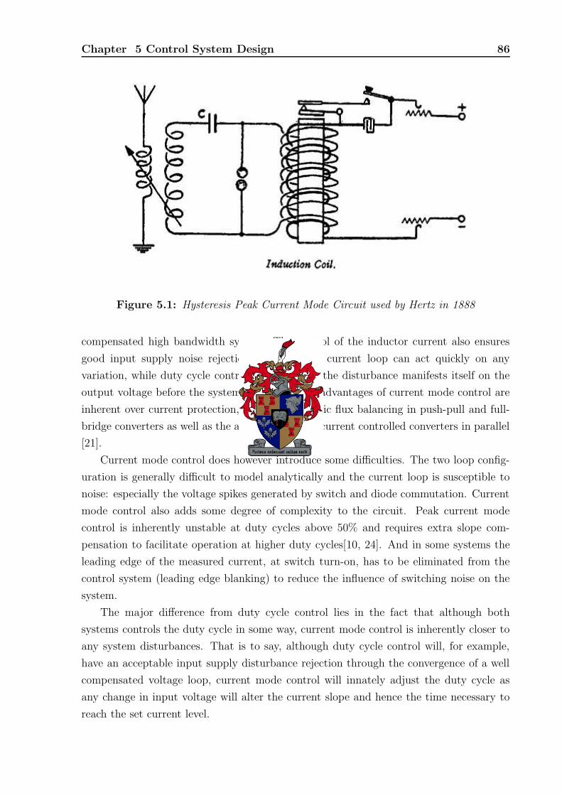
Chapter 5 Control System Design 86
Figure 5.1: Hysteresis Peak Current Mode Circuit used by Hertz in 1888
compensated high bandwidth system. The control of the inductor current also ensures
good input supply noise rejection, as the faster current loop can act quickly on any
variation, while duty cycle control demands that the disturbance manifests itself on the
output voltage before the system can act. Other advantages of current mode control are
inherent over current protection, dynamic magnetic flux balancing in push-pull and full-
bridge converters as well as the ability to operate current controlled converters in parallel
[21].
Current mode control does however introduce some difficulties. The two loop config-
uration is generally difficult to model analytically and the current loop is susceptible to
noise: especially the voltage spikes generated by switch and diode commutation. Current
mode control also adds some degree of complexity to the circuit. Peak current mode
control is inherently unstable at duty cycles above 50% and requires extra slope com-
pensation to facilitate operation at higher duty cycles[10, 24]. And in some systems the
leading edge of the measured current, at switch turn-on, has to be eliminated from the
control system (leading edge blanking) to reduce the influence of switching noise on the
system.
The major difference from duty cycle control lies in the fact that although both
systems controls the duty cycle in some way, current mode control is inherently closer to
any system disturbances. That is to say, although duty cycle control will, for example,
have an acceptable input supply disturbance rejection through the convergence of a well
compensated voltage loop, current mode control will innately adjust the duty cycle as
any change in input voltage will alter the current slope and hence the time necessary to
reach the set current level.

Chapter 5 Control System Design 87
Q
Q SET
CLR
S
R
Clock
Voltage Reference
pwm -
+
Figure 5.2: Peak Current Mode Control
Several methods of current mode control exists. A large class distinction can be made
between the different methods; constant and variable frequency operation. Peak and
average current mode control would fall under the fixed frequency group while methods
such as tolerance band, hysteric, current mode control would result in variable frequency
operation. The design of a transformer system for operation at a range of frequencies is
however, complex. To this end, variable frequency control algorithms has been eliminated
from this study.
5.1.1 Peak Current Mode Control
Peak current mode control utilizes the instantaneous value of the switch current for system
control. The implementation of peak current mode in a Buck converter is shown in Figure
5.2. The outer voltage loop compares the desired setting with the actual measured value
to generate an error signal. System compensation is realised through modification of this
error signal. This modified error signal becomes the current command to the inner current
loop, normally only compensated with a high gain.
The control of the maximum switch current magnitude introduces other inherent ad-
vantages. In all topologies this feature introduces a current limiting capability through
clamping the magnitude of the current error signal. This current limiting serves to protect
the system from overloads and high input currents resulting from low input voltage condi-
tions. In some isolated systems such as the flyback and the full-bridge the switch current
also defines the transformer current. Transformer saturation can be prevented through
limiting the instantaneous switch current magnitude to below the saturation threshold.

Chapter 5 Control System Design 88
Clock
Voltage Reference pwm
-
+ + -
Figure 5.3: Average Current Mode Control
Another advantage that stems from the control of the switch current magnitude occurs
in isolated bi-polar converters such as the push-pull and full-bridge. If the error signal
magnitude is comparable from switching half cycle to half-cycle (as the case will be with a
system with an open loop bandwidth equal or less than one half the switching frequency)
the flux excursion in the core will always be nearly symmetrical. This ensures that
no circulating current will be present in the primary circuit and that the magnetising
inductance current will not be inadvertently biased.
5.1.2 Average Current Mode Control
Average current mode control controls the average value of the current through an inte-
grating loop compensation. The integrator in the loop adjusts the duty cycle such that
the integral of the current error is zero, that is to say that the time average of the current
is set at the desired level. This implies that full knowledge of the current signal is re-
quired, while peak current mode control utilises only the current information during the
on-period.
The integrating property of average current mode control ensures a natural noise
resilience. The implementation of average current control, shown in Figure 5.3, clearly
shows the integration of the complete current information. The characteristic shape of
the steady state current error signal, as shown, is a sinusoidal shape from which all high
frequency components has been removed through integration. This characteristic also
ensures stability over all duty-cycle ranges, without the requirement of slope compensation
[9].
The direct control of current also introduces other advantages. In high power factor
switching regulators, such as PFC boost converters, the control of the inductor current
results in input current control. The pre-regulator utilises the high-bandwidth current

Chapter 5 Control System Design 89
loop to program the input current to follow the desired shape, normally a rectified sine
wave with the desired phase shift, normally 0. The control of average current also ensures
a greater degree of control by the outer voltage loop, especially during operation in the
discontinuous conduction mode.
5.1.3 Average versus Peak Current Mode in a ZVS FB Converter
Although both methods of control offer many advantages and indeed share many compared
to duty-cycle control, there are some intrinsic differences between the methods. Average
current mode control through the integration property, controls the time averaged value
of the current. This, as discussed previously, works superbly in single quadrant converters
where the controlled current is unidirectional. In the aforementioned boost converter this
control scheme results in precise time averaged input current control, or alternatively in
a buck converter the control scheme regulates the output current of the system.
However, this time averaged property of average current mode control in bidirectional
converters, such as push-pull or full-bridge, results in a loss of information. Since the
combined current through the two half-legs is averaged and then controlled, nothing
prohibits the system from introducing an imbalance between the half-leg currents. In
isolated supplies this, undesirable effect, becomes crucial as any imbalance between the
half-leg currents results in a flux imbalance in the transformer. This flux imbalance might
result in magnetising inductance saturation. This saturation, once it occurred, results in
a right-hand pole response in that the saturated inductance will cause an increase of the
already amplified half leg current.
This imbalance between the half leg currents can only be rectified through the addition
of a capacitor to provide integral voltage-time balance and hence flux balance in the
transformer. However, at large voltage levels the size of this capacitor makes this solution
unfeasible. Besides, the voltage integration property of the capacitor effectively reduces
the available input voltage and reduces the power output capacity of the converter.
Peak current mode control on the other hand provides inherent flux balance in isolated
converters in that the peak value of the two half leg currents are controlled. By effectively
limiting the allowable peak current, the flux peak in the transformer can be limited to
below the saturation barrier. In the ZVS-FB converter with a current doubling rectifier,
peak current mode control has the added advantage that the two output inductor currents
are controlled. This results in equal average currents in the two inductors and eliminates
the undesirable possibility of a current reversal in one of the inductors.
All in all peak current mode control due to the inherent flux balancing property is
best suited to the application at hand.

Chapter 5 Control System Design 90
5.2 Small-Signal Modelling of Current Mode Control
Small-signal modelling of the complete circuit is a helpful tool in system optimisation.
The switching behaviour of a converter added to the characteristics of the circuit ele-
ments ensues that the power conversion is a non-linear process. This non-linearity is an
undesirable attribute as most analytical tools such as the Laplace transform is useless in
a non-linear environment. Small-signal analysis of a system often includes a linearisation
step around a work-point to counter act this non-ideal behaviour.
Several methods of small-signal analysis exist. State-space averaging has been pro-
posed by Middlebrook and Cuk in 1976 [23] and is discussed in [24, 10]. State-space
averaging utilise the state-space small-signal model of the system to perturb and linearise
the model. Another small-signal model is the use of the equivalent switch model sug-
gested by Vatche Vorperian [52, 51]. Average switch modelling has specific application in
current mode control systems, as the current information is extractable from the system
model, in comparison with the state-space averaging model where current information in
different states might incur manipulation of the characteristic system matrix.
Using the average switch model the characteristic behaviour and signal flows of peak
current mode can be investigated and modelled. In the next sections a model of peak
current mode will be developed, covering the inherent discretisation of the error signal
and the gains included in the system. Much of the following sections are discussed in
[34, 15, 19] but is repeated here to provide a sense of continuity.
5.2.1 Small-Signal Current Modulator Gain
Most modern switch mode converters are controlled by a direct manipulation of the duty
cycle. Accordingly, a wealth of literature exists describing the small-signal behaviour of
various converter configurations as a function of the applied duty cycle. However, in
current mode control, the duty cycle is not controlled directly, by straight comparison
of an error signal and a reference waveform, as is the case with ‘normal’ voltage mode
control, but is a function of many variables. Under small-signal conditions, in steady
state, many of these influences can be ignored and a feasible transfer function can be
constructed to describe the error voltage to duty cycle transformation.
Investigation of the waveforms of the general PCMC case, with the addition of slope
compensation, reveals insight into the transfer function. With reference to Figure 5.4 let
VGS be the applied switching signal, RsIL be the voltage corresponding to the inductor
current, typically sensed through a resistor Rs and vs the slope compensation voltage.
The current command is represented by Vc. If rising slope of the sensed inductor current
is given as Mr it follows that;
Mr = tanα =AB
dTs
=∆ILRs
DTs
(5.1)
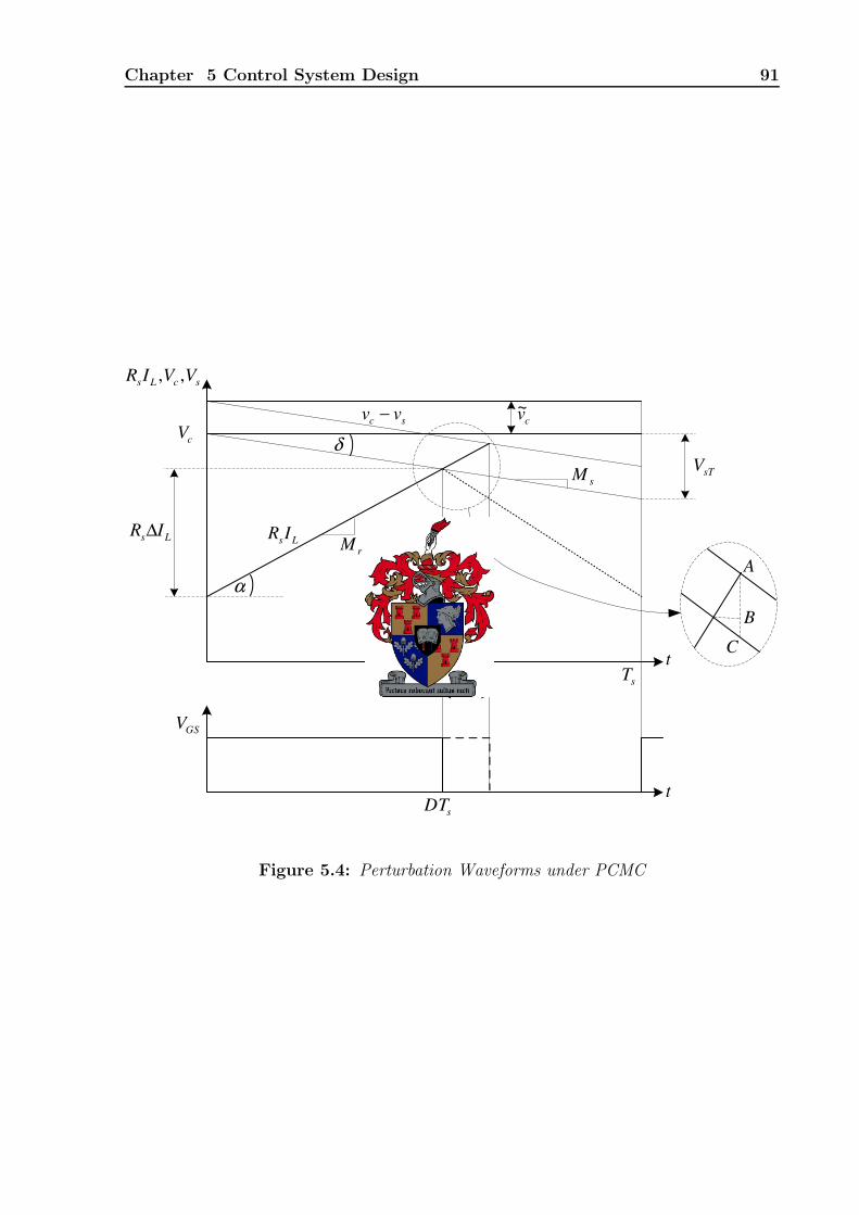
Chapter 5 Control System Design 91
α
δ
rM
sM
sTd~
sT
sDT
Ls IR ∆
cv~
cV
scLs VVIR ,,
GSV
sTV
sc vv −
LsIR
A
B
Ct
t
Figure 5.4: Perturbation Waveforms under PCMC

Chapter 5 Control System Design 92
and with the slope of the slope compensation given as Ms it follows that;
Ms = tan δ =BC
dTs
=VsT
DTs
(5.2)
Investigation of Figure 5.4 in combination with equations 5.1 and 5.2 reveals that
vc = AC = AB + BC = (Mr + Ms)dTs (5.3)
∴ Hm ≡ d
vc
=1
(Mr + Ms)Ts
(5.4)
From equation 5.4 it is clear that the addition of slope compensation reduces the
modulator gain. The modulator gain can become extremely high as the rising current
slope decreases, typically at higher duty cycles. However, the addition of ‘gain’ to the
system does not effectively account for the inherent stability margin in peak current mode
control, i.e. a duty cycle smaller than 0.5 [10]. This boundary is clear upon investigation
of the control waveforms with D > 0.5 and no slope compensation. Figure 5.5 shows the
inability of the control scheme to remedy a perturbation of the inductor current, expressed
as RsIL.
Equation 5.4 does not allow for this sudden stability boundary. The equation was
derived through investigation of a single switching cycle and can thus not account for the
instability. Moving from this statement it is proposed that the modulator gain is valid
in as much as the stability boundaries are adhered to. From this statement it is clear
that a certain loss of information has taken place in that the explicit small-signal model
of the system does not account for this instability. It is fair to admit however, that this
instability is a function of the steady state operating point of the system. Care must be
taken to ensure that the system never operates outside the stability margins.
5.2.2 The Discretisation of the Error-Signal
If, under steady state conditions, it is assumed that the rising and falling slopes of both the
ideal and perturbed inductor currents are equal, then the controller exhibits characteristics
of a sample-and-hold system. Figure 5.6 shows the error between the ideal and perturbed
currents over time. Now since the control voltage Vc is a function of this error, this
phenomenon must be taken into consideration.
The current error wave form in Figure 5.6 can be simplified by ignoring the finite
rising and falling edges to form a perfect sample-and-hold system. Manipulation of the
system information reveals [34],
iL(k + 1) = −αiL(k) +1
Rs
(1 + α)vc(k + 1) (5.5)
α =Mf − Ms
Mr + Ms
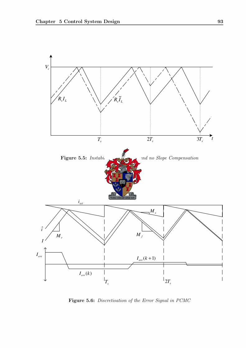
Chapter 5 Control System Design 93
sT sT2 sT3
cV
LsIRLsIR
~
t
Figure 5.5: Instability with d > 0.5 and no Slope Compensation
sT sT2
errI
I
)(kIerr
)1( +kIerr
rM fM
sM
seti
i
Figure 5.6: Discretisation of the Error Signal in PCMC

Chapter 5 Control System Design 94
The Z-transform of equation 5.5 follow as:
Hd(Z) ≡ iL(Z)
vc(Z)=
1
Rs
(1 + α)Z
Z + α(5.6)
Ignoring the effect of the scaling Rs, the poles of the control current to output current
transfer function is Z = −α. When Mr < Mf , implying D > 0.5, the root will be outside
the unit circle, i.e. α > 1. Hence the system will be unstable for duty cycles greater than
0.5.
Also note that the current error is sampled at the switching frequency. According
to the Nyquist criteria, no signal with a bandwidth of more than half the sampling rate
can be accommodated without the loss of information. Under PCMC the error signal
bandwidth must be kept within the bounds set by the Nyquist criteria or the system
will exhibit unstable behaviour. This can be set as a boundary condition of the control
system.
vc(s) ∑ verrHCG(s)
´verrHm(s) d
HP (s)
iL(s)
Rs
vLHe(s)
vL
−
Figure 5.7: Simplified Block Diagram of PCMC
Manipulation of equation 5.6 results in a continuous time expression for the vc to iL
transfer function. Since this expression was derived from the switching waveforms of the
system, it encompasses the complete circuit behaviour, with the inclusion of the sampling
effect and all the system gains. The s-domain expression is [34];
Hd(s) ≡ierr(s)
vc(s)=
1
Rs
1 + α
sTs
esTs − 1
esTs − α(5.7)
Direct comparison of this equation with Figure 5.7 reveals that, with the control gain
HCG(s) = 1, this transfer function can also be expressed as;
Hd(s) =Hm(s)HP (s)
1 + RsHe(s)Hm(s)HP (s)(5.8)
Through investigation of the switching and control waveforms, with the incorporation
of the average switch model, the plant gain, HP (s), can be found for all converters. If the
steady state assumptions are valid, i.e. Mr and Mf are constant, then;
HP (s) ≡iL(s)
d(s)=
Mr + Mf
sRs
(5.9)

Chapter 5 Control System Design 95
Direct manipulation of equations 5.7, 5.8 and 5.9 results in the discretisation gain [34];
He(s) =sTs
esTs − 1(5.10)
5.2.3 Representation of He(s) in the System Model
Direct representation of e−sT in a finite model proves to be difficult as the characteris-
tic roots of the expression are infinite in number. Some approximation must be made
to limit the number of poles while preserving the characteristics of the system. Pade
approximations are used to model this time delay in control systems [11].
The Pade approximation of a time delay does however exhibit imperfect behaviour.
Ideally the step response of the approximation should exhibit no discontinuity at t = 0 and
in the frequency domain the gain of the system should be flat with a gradual increase of
phase shift with an increase in frequency. Unfortunately these requirements are mutually
exclusive.
The Pade approximation of a system can be given as [48];
Pm,n(x) =Rm(x)
Qn(x)(5.11)
Rm(x) =
m∑
k=0
(m + n − k)!m!
(m + n)!k!(m − k)!(−x)k
Qn(x) =n∑
k=0
(m + n − k)!n!
(m + n)!k!(n − k)!xk
A Pade approximation (of the time delay system) with equal powers of s in the numer-
ator and denominator results in a good approximation in the frequency domain, while the
step response yields an unacceptable discontinuity at t = 0. While an approximation with
a second order denominator and a first order numerator results in a better approximation
in the time domain but exhibits a first order decrease in gain due to an uncompensated
pole [48].
Several approximations of the time delay function can be made by either increasing
the order of both the numerator and denominator or by using functions of different orders.
Some approximating functions are shown;
P22(s) =(sTs)
2 − 6sTs + 12
(sTs)2 + 6sTs + 12(5.12)
P12(s) =− 2sTs + 6
(sTs)2 + 4sTs + 6(5.13)
P14(s) =120 − 24sTs
120 + 96sTs + 36s2T 2s + 8s3T 3
s + s4T 4s
(5.14)
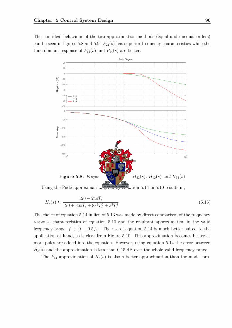
Chapter 5 Control System Design 96
The non-ideal behaviour of the two approximation methods (equal and unequal orders)
can be seen in figures 5.8 and 5.9. P22(s) has superior frequency characteristics while the
time domain response of P12(s) and P14(s) are better.
Bode Diagram
Frequency (rad/sec)
Pha
se (d
eg)
Mag
nitu
de (d
B)
−60
−50
−40
−30
−20
−10
0
10
20
P22P12P14
104
105
106
−450
−360
−270
−180
−90
0
Figure 5.8: Frequency Response of H22(s), H12(s) and H14(s)
Using the Pade approximation given by equation 5.14 in 5.10 results in;
He(s) ≈120 − 24sTs
120 + 36sTs + 8s2T 2s + s3T 3
s
(5.15)
The choice of equation 5.14 in lieu of 5.13 was made by direct comparison of the frequency
response characteristics of equation 5.10 and the resultant approximation in the valid
frequency range, f ∈ [0 . . . 0.5fs]. The use of equation 5.14 is much better suited to the
application at hand, as is clear from Figure 5.10. This approximation becomes better as
more poles are added into the equation. However, using equation 5.14 the error between
He(s) and the approximation is less than 0.15 dB over the whole valid frequency range.
The P14 approximation of He(s) is also a better approximation than the model pro-

Chapter 5 Control System Design 97
Step Response
Time (sec)
Am
plitu
de
0 0.5 1 1.5 2 2.5 3 3.5 4 4.5 5
x 10−5
−0.4
−0.2
0
0.2
0.4
0.6
0.8
1
1.2
P22P12P14ideal
Figure 5.9: Step Response of H22(s), H12(s) and H14(s)
104 105
0.5
1
1.5
2
2.5
3
3.5
w (rad/s
Gai
n (d
B)
104 105
−80
−60
−40
−20
w (rad/s)
degr
ees
IdealP12P14
Figure 5.10: Frequency Response of He(s) and Approximating Functions

Chapter 5 Control System Design 98
posed by Ridley [34];
He(s) ≈ 1 +s
Qnωn
+s2
ω2n
(5.16)
Qn =− 2
Ts
ωn =π
Ts
Over the valid frequency range equation 5.15 has a RMS error (expressed in dB) of 0.0005
compared to equation 5.16 weighing in at 0.011.
5.3 Modelling of the ZVS Full-Bridge Converter under Peak Current
Control
Inspection of the ZVS phase shifted full-bridge topology with a current doubling rectifier
reveals two isolated, current controlled buck converters, operating in parallel and sharing
the same low-pass filter. With reference to Figure 5.11, the buck converter formed by
switches 1 and 4 in conjunction with the transformer and output filter is essentially in
parallel with the converter formed by switches 2 and 3. These buck converters operate in
an alternating fashion. The two output inductor currents, each influenced by one of the
buck converters, are indirectly controlled by controlling the switch currents. The system
can thus be modeled as two peak current controlled converters sharing the same load and
output filter as well as input variables [19].
1 2
3 4
Figure 5.11: ZVS Full-Bridge Topology
5.3.1 Derivation of the Transfer Functions
With reference to section A.1 the switch of the equivalent converter can be represented
by the average switch model. Under transient conditions the unchanging nature of the

Chapter 5 Control System Design 99
−+
Vdcd1
L1
I1
r1
rc
C
R
r2 L2
I2
−+
Vdcd2
Figure 5.12: Equivalent Circuit of ZVS FB under Transient Conditions
steady state elements can be ignored and only the small-signal elements influence the
equivalent circuit. Hence the equivalent of the two coupled buck converters under transient
conditions can be reduced to the equivalent in Figure 5.12. The system is represented in
block diagram form in Figure 5.13
I(s)
∑Fm(s)
d1H11(s)
∑
I1
∑
RsHe(s)−
∑Fm(s)
d2H11(s)
∑
I2
RsHe(s)−
H12(s)
H12(s)
I0(s)
Figure 5.13: Block Diagram of the ZVS-FB under PCMC
From the equivalent circuit is is clear that some form of interaction will exist between
the two buck converters. The duty cycles d1 and d2 will also not be perfectly equal since
the control scheme will adapt the duty cycle to any imperfections either of the two circuits.
Thus should the value of L2 be slightly larger than L1, d2 will adapt to the value needed
to ensure that the peak current through L2 still conforms to the setting prescribed by the
error signal.
Four independent transfer functions can be identified in the system; being the influence
of the variables d1 and d2 on the outputs I1 and I2. Neglecting any imperfections in the
matching of the two circuits it is clear that both forward transfer functions as well as the

Chapter 5 Control System Design 100
two cross-coupled transfer functions must be equal. Analysis of the forward path reveals;
H11(s) =I1(s)
d1(s)=
s2 CL2(R + rc) + s L2 + C(Rrc + Rr2 + r2rc) + R + rc
αS3 + βS2 + χs + δ
α = CL1L2(R + rc) (5.17)
β = CL1R(r2 + rc) + CL2R(r1 + rc) + L1L2 + CL1rcr2 + CL2rcr1
χ = L1(R + r2) + L2(R + r1) + CRrc(r1 + r2) + Cr1r2(R + rc)
δ = Rr1 + Rr2 + r1r2
which curiously differs significantly from the transfer function proposed by Kutkut [19].
The transfer functions proposed by Kutkut are given as
H11(s) =Vdc
L1 + L2
·s2L2C +
(
RpC + L2
Rt
)
s + RRt
s[
s2LpC +(
RpC + Lp
Rt
)
s + RRt
] (5.18)
H12(s) =−Vdc
L1 + L2·
sRpC + RRt
s[
s2LpC +(
RpC + Lp
Rt
)
s + RRt
] (5.19)
where,
Lp = L1‖L2
Rp = R‖rc
Rt = R + rc
for the forward and cross coupled situations respectively. However Kutkut based this
information on [33] which in turn is valid for two paralleled duty cycle controlled buck
converters each with its own capacitive output filter. A casual inspection of equations
5.17 and 5.18 reveals the discrepancy of the low frequency pole, Kutkut place this pole
at the origin while the complete solution places this pole, with the designed values, at 40
rad·s−1.
Since the system is desired to operate as an ideal current source, no output capacitance
is added to the system. If the output capacitance is excluded form the analysis the transfer
function can be simplified significantly.
H11 =sL2 + R + r2
s2L1L2 + s(L1R + L2R + L1r2 + L2r1) + Rr1 + Rr2 + r1r2
(5.20)
With the designed values of L1 = L2 = 1 mH and an output capacitance of 100 pF the
corresponding frequency responses of the complete and simplified transfer functions are
shown in Figure 5.14. The extra zero, attributable to the output capacitance, is clearly
visible in both the phase and gain responses, with the capacitance pole only evident in
the phase response at extremely high frequencies. The simplification is justified in that
the low frequency responses are identical.

Chapter 5 Control System Design 101
Comparison with the transfer function proposed by Kutkut reveals that the high fre-
quency response is similar to the proposed transfer function. However, the response differs
dramatically below the low frequency pole of the proposed transfer functions. The gain
comparison reveals that for frequencies higher than 16 Hz the response is similar while
the phase responses are comparable above 420 Hz. A comparison of the simplified trans-
fer function, without the addition of the output capacitance, and the transfer function
proposed by Kutkut is included in Figure 5.15.
Bode Diagram
Frequency (rad/sec)
Pha
se (d
eg)
Mag
nitu
de (d
B)
−80
−60
−40
−20
0
20
40
Complete ModelSimplified Model
10−1
100
101
102
103
104
105
106
−90
−45
0
Figure 5.14: Bode Plot of the Derived Transfer Functions
The cross-coupled transfer functions can be found in a similar manner. This transfer
function with the inclusion of the output capacitance is found as;
H12(s) =I2(s)
d1(s)=
sCRrc + R
αS3 + βS2 + χs + δ(5.21)
α = CL1L2(R + rc)
β = CL1r2(R + rc) + CL2r1(R + rc) + L1L2 + CRrc(L1 + L2)
χ = L1r2 + L2r1 + Cr1r2(R + rc) + CRrc(R1 + r2) + R(L1 + L2)
δ = r1r2 + Rr1 + Rr2
When the effect of the ouput capacitance in neglected the transfer function can be sim-
plified to
H12(s) =R
s2L1L2 + sL1(R + r2) + sL2(R + r1) + Rr1 + Rr2 + r1r2(5.22)

Chapter 5 Control System Design 102
Bode Diagram
Frequency (rad/sec)
Pha
se (d
eg)
Mag
nitu
de (d
B)
−100
−50
0
50
100
Transfer Function Proposed by KutkutSimplified Derived Transfer Function
10−1
100
101
102
103
104
105
106
−90
−45
0
Figure 5.15: Comparison of the Derived Forward Transfer Function and the Transfer
Function Proposed by Kutkut
The response of this simplified transfer function is perfectly similar to the complete
transfer function of equation 5.21 at all applicable frequencies. However, comparison with
the transfer function proposed by Kutkut reveals, once again, discrepancies in his proposed
approximation. The comparison of the two transfer functions is included in Figure 5.16.
The gain and phase information of the two alternatives are once again comparable above
16 Hz and 420 Hz, respectively.
5.3.2 Derivation of the System Transfer Function
The block diagram of the system can be represented in signal flow diagram form as
indicated in Figure 5.17. It is clear that there are four forward paths and four feedback
paths. The paths and their relative gains are indicated in Table 5.1. The transfer functions
are defined, with reference to Figure 5.13, as;
F = Fm(s)H11(s) (5.23)
C = Fm(s)H12(s) (5.24)
G = RsHe(s) (5.25)

Chapter 5 Control System Design 103
Bode Diagram
Frequency (rad/sec)
Pha
se (d
eg)
Mag
nitu
de (d
B)
−150
−100
−50
0
50
100Transfer Function Proposed by KutkutSimplified Derived Transfer Function
10−1
100
101
102
103
104
105
106
0
45
90
135
180
Figure 5.16: Comparison of the Derived Cross Transfer Function and the Transfer
Function Proposed by Kutkut
Ic(t) 1
2
F
3
4
F
5
6 I0(t)
CC
−G
−G
Figure 5.17: Signal Flow Diagram for the ZVS-FB under PCMC

Chapter 5 Control System Design 104
Path Gain
Forward Paths
1236 F
1256 C
1456 F
1436 C
Feedback Paths
232 -FG
25432 C2G2
454 -FG
43242 C2G2
Table 5.1: Signal Flow Graph Path Gains
The equivalent transfer function of the complete system can be found to be
H(s) =
∑
i Pi∆i
∆(5.26)
∆ = 1 − (2C2G2 + 2FG) + F 2G2 (5.27)
∆1,3 = 1 + FG (5.28)
∆2,4 = 1 (5.29)
H(s) =2F (1 + FG) + 2C
1 − 2FG − 2C2G2 + F 2G2(5.30)
5.4 An Alternative Cross-Coupled Signal Model
The approach followed by Kutkut fails to describe the true behaviour of the converter in
many aspects, as shown in the previous section. The main failure of the approach lies in
the definition of the cross-coupled functions. Each buck converter operates independently
from the other in virtually every aspect with the exception of a shared output filter. The
peak magnitude of the current in each inductor will be controlled to the value set by each
independent current control loop.
There is however a cross coupling between the two loops. The average value of the
inductor current is not perfectly defined by the peak value of the inductor current. This
statement is validated in the fact that the current ripple of the inductors are not fixed.
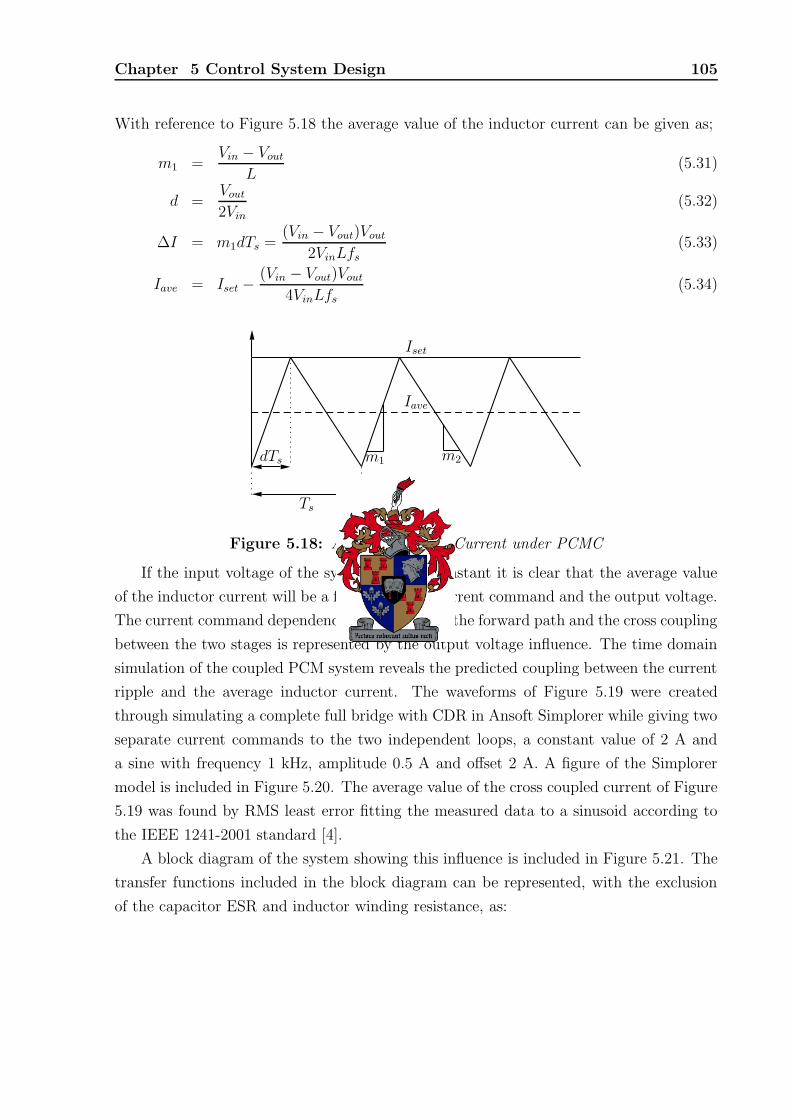
Chapter 5 Control System Design 105
With reference to Figure 5.18 the average value of the inductor current can be given as;
m1 =Vin − Vout
L(5.31)
d =Vout
2Vin
(5.32)
∆I = m1dTs =(Vin − Vout)Vout
2VinLfs
(5.33)
Iave = Iset −(Vin − Vout)Vout
4VinLfs
(5.34)
Iset
Iave
Ts
dTs m1 m2
Figure 5.18: Average Inductor Current under PCMC
If the input voltage of the system remains constant it is clear that the average value
of the inductor current will be a function of the current command and the output voltage.
The current command dependency corresponds to the forward path and the cross coupling
between the two stages is represented by the output voltage influence. The time domain
simulation of the coupled PCM system reveals the predicted coupling between the current
ripple and the average inductor current. The waveforms of Figure 5.19 were created
through simulating a complete full bridge with CDR in Ansoft Simplorer while giving two
separate current commands to the two independent loops, a constant value of 2 A and
a sine with frequency 1 kHz, amplitude 0.5 A and offset 2 A. A figure of the Simplorer
model is included in Figure 5.20. The average value of the cross coupled current of Figure
5.19 was found by RMS least error fitting the measured data to a sinusoid according to
the IEEE 1241-2001 standard [4].
A block diagram of the system showing this influence is included in Figure 5.21. The
transfer functions included in the block diagram can be represented, with the exclusion
of the capacitor ESR and inductor winding resistance, as:

Chapter 5 Control System Design 106
0 0.2 0.4 0.6 0.8 1 1.2 1.4 1.6 1.8 2
x 10−3
0.8
1
1.2
1.4
1.6
1.8
2
time (s)
Indu
ctor
Cur
rent
(A)
Figure 5.19: Cross-Coupling Between the Two PCM Loops in Time
Hi(s) =I(s)
V (s)=
s1
L+
1
LCR
s2 + s1
RC+
1
LC
(5.35)
Hv(s) =V (s)
I(s)=
R
sCR + 1(5.36)
The proposed block diagram of Figure 5.21 was simulated with MATLAB Simulink,
using the same input and circuit parameters as the Simplorer simulation. The results of
the two simulations compare very well and the model can be verified. The results for the
forward and cross transfer functions are included in Figures 5.22 and 5.23. The oscillatory
nature of the Simulink simulated current is due to the high loop gain of the closed PCMC
loop coupled with the time delay of the He feedback transfer function, as described in
section 5.2.2.

Chapter 5 Control System Design 107
TWTTWT
-340.00m
3.92
0
2.00
0 2.01m1.00m
2DGraphS...
L1.I [A] L2.I [A] R1.I [A]
Q=>BSQ=>BS
PWM
PWM
Q=>BSQ=>BS
Q=>BSQ=>BSCONST
AND2 AND2
Q=>BSQ=>BS
S Q
QB
Latch
R
S Q
QB
Latch
R
INVINV
NOR2 NOR2
INVINV
AND2 AND2
S Q
QB
Latch
R
S Q
QB
Latch
R AND2 AND2
INVINV AND2 AND2
TWT1
S2 S4
S1 S3
E1
L1
L2
CR1
D1
D2
current_L2
PWM1
PWM2
OmniCaster2
current_L1CONST2
OmniCaster4
lsr1inv1
nor21inv2
lsr2inv3
SINE1
D3 D4
D5 D6
Figure 5.20: Simplorer Model to Investigate the Cross-Coupling

Chapter 5 Control System Design 108
Ic1 ∑ IεFm
d1Vin
+ ∑ d1Vi − Vo Hi(s)I1
+∑I0Hv(s)
V0
−
RsHe(s)
−
Ic2 ∑ IεFm
d2Vin
+ ∑ d2Vi − Vo Hi(s)I2
+
RsHe(s)
−
I0
−
Figure 5.21: Modified Block Diagram to Account for Ripple Cross Coupling
0.2 0.4 0.6 0.8 1 1.2 1.4 1.6 1.8 2
x 10−3
0.6
0.8
1
1.2
1.4
1.6
1.8
2
2.2
2.4
2.6
time (s)
Indu
ctor
Cur
rent
(A)
Current CommandSimplorer CurrentSimulink Current
Figure 5.22: Simplorer and Simulink Simulated Currents for the Forward Transfer
Function

Chapter 5 Control System Design 109
0.2 0.4 0.6 0.8 1 1.2 1.4 1.6 1.8 2
x 10−3
0.8
1
1.2
1.4
1.6
1.8
2
2.2
2.4
time (s)
Indu
ctor
Cur
rent
(A)
Simplorer CurrentSimulink Current
Figure 5.23: Simplorer and Simulink Simulated Currents for the Cross-Coupled
Transfer Functions
Derivation of the Cross Coupled Transfer Function
With reference to Figure 5.18 the small-signal cross coupling transfer function can be
derived as follows:
Vout = Vout + vo (5.37)
Iave + io =[Vin − (Vout + vo)](Vout + vo)
4VinLfs
(5.38)
Iave + io =VinVout − V 2
out − 2Voutvo + Vinvo − v20
4VinLfs
(5.39)
Neglecting the steady state terms of VinVout and V 2out as well as the nonlinear v2
0 term the
dependency simplifies to:
io =vo(Vin − 2Vout
4VinLfs
(5.40)
io =vo(1 − 4D)
4Lfs
(5.41)
From Figure 5.12 the output voltage response due to a variation in duty cycle of one
converter-half can be found. The transfer function van be represented, in non-canonical
form, as:
Hv(s) =Vout(s)
D(s)=
R(sCrc + 1)
s2LC(R + rc) + s L + C(R + rc) + CRrc + R + rL
(5.42)

Chapter 5 Control System Design 110
The cross-coupled transfer function can be given as, with reference to Figure 5.13,
H12(s) =I1(s)
D2(s)=
I2(s)
D1(s)=
1 − 4D
4Lfs
Hv(s) (5.43)
The system transfer function can be found, using the newly derived cross coupled
transfer functions, through application of Mason’s rule on the signal flow graph of Figure
5.17. As described in section 5.3.2.
5.5 Slope Compensation
The instability of PCMC circuits under high duty cycles are well known and documented
[15, 34, 19, 21] and is also discussed in section 5.2. The existence of the instabilty of the
PCMC loop under higher duty cycles is due to the gain of the modulator which increases
toward infinity as the on-time current slope decreases. Equation 5.4 is repeated here for
convenience
Fm =1
(Mr + Ms)Ts
(5.44)
where Mr and Ms represents the rising on-time sensed current slope and the added slope
compensation slope respectively. It is clear that without slope compensation, i.e. Ms = 0
the modulator gain would approach infinity as the rising current slope approaches zero.
The rising current slope will, for a buck converter, strive toward zero as the output voltage
approach the input voltage, implying duty cycles above 0.5.
The block diagram of a PCMC Buck converter is shown in Figure 5.24. The open
loop gain of the system can be given as FmH(s)RsHe(s), where the transfer function H(s)
will correspond to the forward transfer function H11 found in section 5.3. If the open loop
frequency response of the system is plotted, with a modulator gain of 1, it is can be found
that the system gain at 180 phase shift is 11.9 dB. The frequency response of the system
is displayed in Figure 5.25.
Ic(s) ∑Fm
d1Vin H(s)
I0(s)
RsHe(s)−
Figure 5.24: Block Diagram of a Buck Converter Under PCMC
For conditional stability the open loop gain of the system must be reduced by at least
11.9 dB to reduce the gain to 0 dB at the phase cross-over point. This corresponds to
a Fm value of 0.254, or with the design values of the converter a minimum current rise
slope of 196.8 mAµs−1, with a Rs conversion ratio of 1 VA−1. For this buck converter this

Chapter 5 Control System Design 111
Bode Diagram
Frequency (rad/sec)
Pha
se (d
eg)
Mag
nitu
de (d
B)
−300
−250
−200
−150
−100
−50
0
50
100
101
102
103
104
105
106
107
108
109
1010
−450
−360
−270
−180
−90
0
Figure 5.25: Open Loop Frequency Response of a Buck Converter Under PCMC with
Fm = 1
value would correspond to a maximum duty cycle of 50.8 %, incidently the same value
found in section 5.2.
For the current doubling rectifier it is known that the individual current loop duty
cycles never exceed 50 % as the two loops are swiched in an alternating, constant fre-
quency fashion. Neglecting the effect of the cross-coupling between the two PCMC buck
converters in the CDR, which is reasonable as the cross-coupled loop maximum gain is
less than -40 dB, the open loop response of each of the converters would correspond to
that of the discussed buck converter. This would imply that the maximum value of the
modulator gain Fm will also be 0.254. The current doubling rectifier operates such that
the input voltage of the “Buck converter” on the secondary of the transformer will always
be at least twice the value of the output voltage. For this design the minimum value of
current rise slope can be given as;
Mr(min) =Vin − Vout(max)
L= 200mAµs−1 (5.45)
This current rise slope would correspond to a stable system under all operating conditions
although the phase margin at higher output duty cycles will be very low, resulting in a
severely deteriorated transient response.
To keep the phase margin under all conditions above 40 the gain must be reduced,
from the nominal value of Fm = 1 as displayed in Figure 5.25, to 0.2065 under all condi-
tions. From equation 5.44 the value of the added slope can be found as 42 mAµs−1

Chapter 6System Evaluation
“Theories and ideas have almost no value at all in our world. Laboratory demonstrations
are worth very slightly more . . . it is only a properly engineered device that has real value.”
Kenneth Shoulders
Since the system consists of many coexistent yet orthogonal subsystems, the operational
verification of the complete system can be subdivided into a thorough evaluation of
each subsystem. Only after the operation of each subsystem had been scrutinised and
verified, would it logically make sense to investigate the operation of the complete system.
Although the minute detail of this verification process is beyond the scope of this text
the main aspects of this process will be discussed.
6.1 Bias Supply Flyback Converter
The two isolated ±15 V supplies that bias the control electronics of the PFC boost
converter and the ZVS phase shift full-bridge converter lies at the heart of the system
operation. Any instability in the supply operation would permeate through the complete
system with unpredictable results. The symptoms caused by incorrect supply rail opera-
tion in the complete system might represent the symptoms of another problem and it is
therefore necessary to ensure the supply rail integrity.
6.1.1 Control System and Stability
The flyback converter is controlled by a peak current mode scheme whereby the duty cycle
of the switching element is governed by the peak value of the current stored in the flyback
transformer magnetising inductance, refer to chapter 5. At the heart of system operation
lies the accurate representation of this current information as any noise might obscure
the vital information and threaten system stability. Although every possible measure has
been taken during the layout to minimise stray inductances the representation of this
information must be verified.
112

Chapter 6 System Evaluation 113
The current information is represented as a voltage and fed into the control system
where it is compared to a control signal voltage. The conversion between the current and
voltage signals take the form of a 250 mΩ sense resistor. In general this conversion process
should be linear, but stray inductances in the current path will superimpose voltages on
this signal, especially during turn-on and turn-off. The signal has been measured and is
represented in Figure 6.1. Although the cross-coupling of the switching information is
−2 −1.5 −1 −0.5 0 0.5 1 1.5 2
x 10−6
−0.2
−0.1
0
0.1
0.2
0.3
Vol
tage
(V)
time (s)
Sensed Current
Figure 6.1: Flyback Sensed Magnetising Current Information
evident on the signal it will not affect the converter operation. The turn-on noise spike
is well contained and well bounded in time and will be filtered out by the leading edge
blanking sub-circuit of the UC3844 switching regulator. The turn-off noise spike, although
more pronounced, occurs after the control decision was made.
The converter feedback loop was compensated by measuring the open-loop system
response in the frequency domain. The outputs were loaded with 125 mW each, which
corresponds to about 20 % of the expected load conditions, to provide a suitable working
point about which to linearise the system.
A variable frequency source was connected to the summing junction shunt regulator
input while the output of the controlled +15 V output was measured. The open loop
gain and phase response is displayed in Figure 6.2. The noise in the phase response
measurement is attributed to the measurement method (using an oscilloscope in the time
domain and measuring the time between the reference and resultant waveforms). From
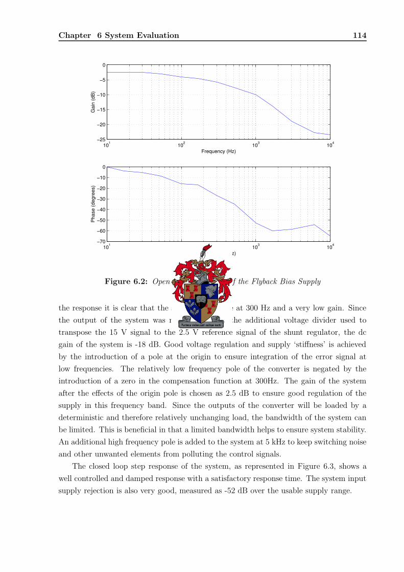
Chapter 6 System Evaluation 114
101 102 103 104−25
−20
−15
−10
−5
0
Gai
n (d
B)
Frequency (Hz)
101 102 103 104−70
−60
−50
−40
−30
−20
−10
0
Pha
se (d
egre
es)
Frequency (Hz)
Figure 6.2: Open Loop Bode Plot of the Flyback Bias Supply
the response it is clear that the system has a pole at 300 Hz and a very low gain. Since
the output of the system was measured before the additional voltage divider used to
transpose the 15 V signal to the 2.5 V reference signal of the shunt regulator, the dc
gain of the system is -18 dB. Good voltage regulation and supply ‘stiffness’ is achieved
by the introduction of a pole at the origin to ensure integration of the error signal at
low frequencies. The relatively low frequency pole of the converter is negated by the
introduction of a zero in the compensation function at 300Hz. The gain of the system
after the effects of the origin pole is chosen as 2.5 dB to ensure good regulation of the
supply in this frequency band. Since the outputs of the converter will be loaded by a
deterministic and therefore relatively unchanging load, the bandwidth of the system can
be limited. This is beneficial in that a limited bandwidth helps to ensure system stability.
An additional high frequency pole is added to the system at 5 kHz to keep switching noise
and other unwanted elements from polluting the control signals.
The closed loop step response of the system, as represented in Figure 6.3, shows a
well controlled and damped response with a satisfactory response time. The system input
supply rejection is also very good, measured as -52 dB over the usable supply range.

Chapter 6 System Evaluation 115
−1 0 1 2 3 4 5 6 7 8
x 10−4
0
2
4
6
8
10
12
14
16
Time (s)
Vol
tage
(V)
Figure 6.3: Closed Loop Step Response of the Flyback Converter
6.1.2 Electro-Magnetic Compatibility
Since all the control elements of the system is powered by the flyback converter any electro-
magnetic noise generated by the supply would permeate through the entire system. Many
of the elements in the system such as the ZVS full-bridge control loop elements would be
sensitive to any noise, especially as the bandwidth of the system would be increased to
the maximum, resulting in a very low gain and phase margin. It is therefore critical to
ensure that the supply is free of both common mode (CM) and differential mode (DM)
noise.
A major contributor to the generation of both CM and DM noise is the switching
behaviour. During turn-off the current flowing through the magnetising inductance is
suddenly referred from the primary winding to the secondary. In an ideal transformer this
process would occur naturally but the leakage inductance of the non-ideal transformer
complicates the turn-off operation slightly. The energy stored in the primary leakage
reactance in the form of a current is suddenly directed to the switch output capacitance
Coss by the turn-off of the current path through the switch body. This closed energy path
will result in an underdamped energy exchange response between the leakage inductance
and Coss occurring at a very high frequency and resulting often in a very high voltage
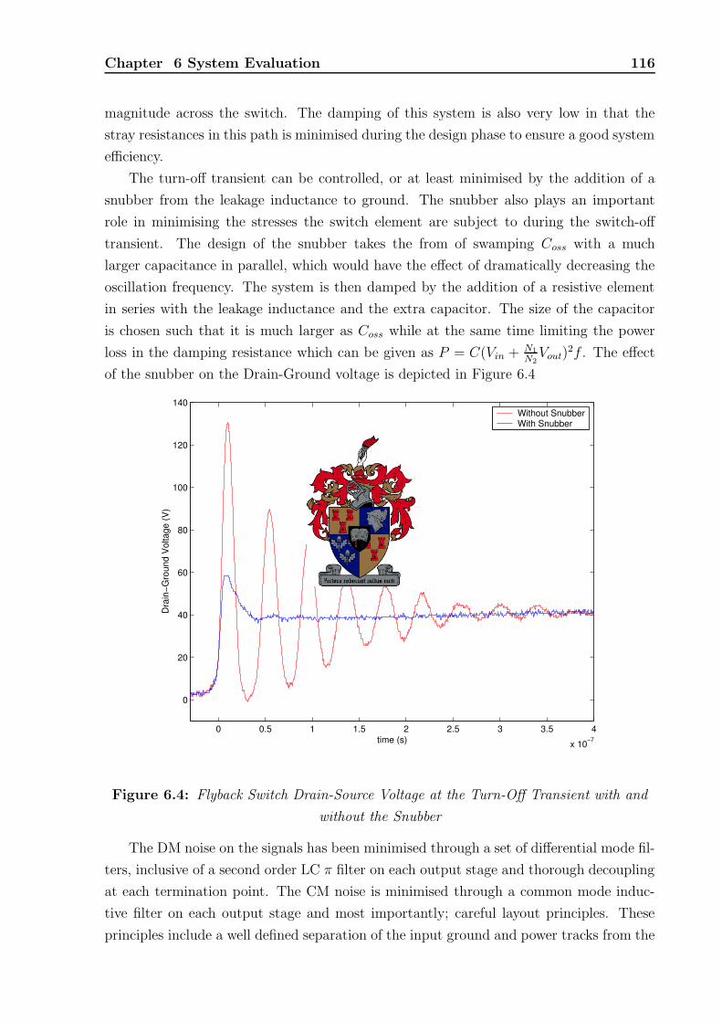
Chapter 6 System Evaluation 116
magnitude across the switch. The damping of this system is also very low in that the
stray resistances in this path is minimised during the design phase to ensure a good system
efficiency.
The turn-off transient can be controlled, or at least minimised by the addition of a
snubber from the leakage inductance to ground. The snubber also plays an important
role in minimising the stresses the switch element are subject to during the switch-off
transient. The design of the snubber takes the from of swamping Coss with a much
larger capacitance in parallel, which would have the effect of dramatically decreasing the
oscillation frequency. The system is then damped by the addition of a resistive element
in series with the leakage inductance and the extra capacitor. The size of the capacitor
is chosen such that it is much larger as Coss while at the same time limiting the power
loss in the damping resistance which can be given as P = C(Vin + N1
N2Vout)
2f . The effect
of the snubber on the Drain-Ground voltage is depicted in Figure 6.4
0 0.5 1 1.5 2 2.5 3 3.5 4
x 10−7
0
20
40
60
80
100
120
140
time (s)
Dra
in−G
roun
d V
olta
ge (V
)
Without SnubberWith Snubber
Figure 6.4: Flyback Switch Drain-Source Voltage at the Turn-Off Transient with and
without the Snubber
The DM noise on the signals has been minimised through a set of differential mode fil-
ters, inclusive of a second order LC π filter on each output stage and thorough decoupling
at each termination point. The CM noise is minimised through a common mode induc-
tive filter on each output stage and most importantly; careful layout principles. These
principles include a well defined separation of the input ground and power tracks from the

Chapter 6 System Evaluation 117
output signals. Although the CM mode noise is difficult to quantify the DM mode noise
can be measured effectively. The DM noise at the ZVS controller is less than 65 mVpp
which is well within reasonable specifications. A waveform depicting this measurement is
included in Figure 6.5.
0 20 40 60 80 100 120 140 160 180 200−40
−30
−20
−10
0
10
20
30
40
Time (us)
Vol
tage
(mV
)
Figure 6.5: Differential Mode Noise on the Flyback Output Signal
6.2 Power Factor Correction Boost Rectifier
The ability of the PFC-boost front end to intercept the current waveform and change it to
a sinusoidal shape lies at the heart of the system operation. The input current waveforms
of the PFC-boost rectifier with and without the active boost is measured and compared.
The time waveforms in Figure 6.6 show clearly the expected distortion of the input
current under uncontrolled rectifier conditions. The current changes suddenly as the input
voltage increase above the capacitor voltage and a large current flows into the storage
capacitor. The figure also indicates the sinusoidal nature of the controlled input current.
It is difficult however to gauge the harmonic content of the signal from the time
waveform. In Figure 6.7 the magnitude of the input current without the active boost is
shown against frequency. The odd harmonic content of the signal is clearly visible.
With the active boost rectifier in the system the input current is almost sinusoidal.
The time based waveform of Figure 6.6 clearly shows a sinusoidal shape with some high

Chapter 6 System Evaluation 118
0 5 10 15 20 25 30 35 40 45 50−4
−3
−2
−1
0
1
2
3
4
Cur
rent
(A)
Time µ s
With Active PFC StagePassive Rectifier
Figure 6.6: Input Current to the Rectifier with and without the Active Boost
0 50 100 150 200 250 300 350 400 450 5000
0.2
0.4
0.6
0.8
1
Frequency (Hz)
Nor
mal
ised
Cur
rent
(A)
Figure 6.7: FFT of the Input Current without the Active Boost

Chapter 6 System Evaluation 119
frequency information superimposed on it. The high frequency information is in part due
to measurement relics due to oscilloscope grounding (since system ground is referenced
to the rectified negative input). However an investigation into the harmonic content of
the signal shows for all practical purposes a perfect sinusoid at line frequencies. The
magnitude of the input current against frequency is shown in Figure 6.8.
0 50 100 150 200 250 300 350 400 450 5000
0.2
0.4
0.6
0.8
1
Frequency (Hz)
Nor
mal
ised
Cur
rent
(A)
Figure 6.8: FFT of the Input Current with the Active Boost Converter
6.3 ZVS Phase Shifted Full-Bridge
6.3.1 Transformer Characterisation
The transformer lies at the heart of the phase shifted full-bridge converter. It is impera-
tive that the transformer must be characterised in at least three areas of concern, namely:
magnetising inductance, leakage inductance and coupling ratio. These measurements are
important to verify the integrity of the transformer. The presence of unwanted airgaps
in the magnetic circuit will be revealed if the measured magnetising inductance varies
substantially from the design value, unwanted airgaps can occur due to cores with hair-
line cracks or improper core-half alignment. The coupling ratio of the transformer will
provide knowledge that the turns ratio is correct. Although the leakage inductance can
be calculated from knowledge of the magnetising inductance and coupling ratio, separate
measurement of this parameter provides a method of verifying the other measurements.

Chapter 6 System Evaluation 120
Leakage Inductance Measurement
The leakage inductance of the transformer is of paramount importance as the soft switch-
ing behaviour of the converter is facilitated by the leakage inductance in the transformer
circuit. The leakage inductance can be calculated through a method similar to the short
circuit test used for 50 Hz power transformers. This method has been developed by the
author.
The transformer, with short-circuited secondary, is placed in the H-Bridge while the
system is operated under peak current mode control and at a low input bus voltage. The
magnetising inductance of the system is neglected since in the short-circuit configuration,
the magnetising inductance is effectively in parallel with the leakage inductance and in
general Lm >> LL. The system is operated at a low bus voltage and under peak current
mode control to limit the input current to the transformer as the shorted secondary
transformer will virtually present a short circuit to normal bus voltage conditions. The
voltage of the two primary terminals is measured as well as the primary current. The
measured waveforms is represented in Figure 6.9.
−0.4 −0.2 0 0.2 0.4 0.6 0.8 1−4
−2
0
2
4
6
8
10
Vol
tage
(V),
Cur
rent
(A)
Time (us)
Primary Terminal 1 VoltagePrimary Terminal 2 VoltagePrimary Current
Figure 6.9: Measured Waveforms of the Short-Circuit Test
The leakage inductance can be calculated through realising that V = L dIdt
. When the
two terminal voltages are subtracted from one another the voltage across the magnetising
inductance is calculated. The value of dIdt
can be extracted from the discrete signal;
dI
dt(n) =
I(n + 1) − I(n)
∆t, 1 ≤ n ≤ ‖I‖ (6.1)

Chapter 6 System Evaluation 121
However, the quantification noise introduced by the oscilloscope makes the implementa-
tion of this method impossible.
Another possible means of calculating the leakage inductance is by extracting the
Fourier series components from the primary current and applied primary voltage sig-
nals. The effective impedance can be calculated at selected frequencies, typically at the
harmonics of the fundamental frequency. Mathematically the Fourier transform can be
expressed as [32];
IP(k) =N−1∑
n=0
IP (n)e−j2πkn
N , k = 0, 1, . . . , N − 1 (6.2)
VP(k) =
N−1∑
n=0
VP (n)e−j2πkn
N , k = 0, 1, . . . , N − 1 (6.3)
IP (n) =
N−1∑
k=0
IP(k)e−j2πkn
N , k = 0, 1, . . . , N − 1 (6.4)
VP (n) =N−1∑
k=0
VP(k)e−j2πkn
N , k = 0, 1, . . . , N − 1 (6.5)
where IP (n) and VP (n) are discrete time signals, at a constant sample rate, of length N
describing the primary current and terminal voltage respectively. Although the signals are
periodic, the sampling process virtually eradicates the periodic nature of the signals and
hence the representation of the signal as a sum of cosines with frequencies at multiples of
the fundamental is not valid. However, decreasing the sampling rate increases the periodic
nature of the signal as more complete cycles are included.
Decreasing the sampling rate also has the effect of increasing the frequency resolution
if the length of the sample remains constant. This statement can be explained by noting
that in equations 6.2 and 6.3 the vectors describing the signal in the frequency domain
will also have length N . The parameters n and k represents a time value and a frequency
value respectively, or alternatively the time stamp and frequency of the entries in equations
6.2-6.5 corresponding to entry n or k can be given as,
tn = nTs, n = 0, 1, . . . , N (6.6)
fk =k
NTs
, k = 0, 1, . . . , N (6.7)
where Ts is the sampling interval or Ts = tn+1−tn, n = 0, 1, . . . , N−1. It is therefore clear
that the frequency resolution in the FFT signal is given by 1NTs
. If N is constant, as it is
with most measurement equipment, the only option to increase the frequency resolution
is by decreasing the sampling rate. The converse is that a decrease in sampling rate
decreases the frequency range over which the FFT is valid, as described by the Nyquist
criteria.

Chapter 6 System Evaluation 122
The magnitude of the FFT signals for the primary current and the applied voltage to
the primary are shown in figures 6.10 and 6.11. The magnitude is normalised with respect
to the magnitude of the fundamental frequency. Inspection of the signal reveals that, with
the assumption that the captured signal is sufficiently periodic, only odd harmonics are
present. The harmonic data-points from the fundamental to the 9th harmonic are also
shown, indicated by the red crosses. The effects of a lowpass filter applied to the signals
are also visible in the figures. The signals were filtered, reversed, filtered again and again
reversed to limit the phase shift introduced by the filter to a minimum.
0 200 400 600 800 1000 120010−4
10−3
10−2
10−1
100
Frequency (kHz)
Nor
mal
ised
Cur
rent
(dB
)
Figure 6.10: FFT of the Primary Current Signal, With Selected Harmonics Indicated
To proceed, two assumptions must be made. Firstly the digitisation effects are ignored
as the sample length is very large and the frequency informtation to the 25th harmonic
of the fundamental frequency can be measured directly. The possibility of errors due to
aliasing is low. Although the signal was not low-pass filtered before discretisation, the
resolution is such that the first harmonic that can influence the measurement is the 39th,
which after folding back will occur close to teh 9th harmonic. Secondly the assumption is
made that due to the reduced sampling rate and hence the inclusion of a large number
of complete cycles in the measured signal the captured signal is periodic. With these
assumptions, equations 6.4 and 6.5 and applying a crude reconstruction of the time-signal
the time signals can be given as:
IP (t + ct) ≈ca
N
h9∑
k=h1,h3
|IP(k)| cos(2kπt
TsN+ ∠IP(k)
)
(6.8)

Chapter 6 System Evaluation 123
0 200 400 600 800 1000 120010−4
10−3
10−2
10−1
100
Frequency (kHz)
Nor
mal
ised
Vol
tage
(dB
)
Figure 6.11: FFT of the Primary Voltage, With Selected Harmonics Indicated
VP (t + ct) ≈ca
N
h9∑
k=h1,h3
|VP(k)| cos(2kπt
TsN+ ∠VP(k)
)
(6.9)
where ct and ca are constants to correct any phase shift or amplitude modulation that
might take place in the process. The symbols h1 through h9 denotes the values of k in IP
and VP that corresponds to the first 9 harmonics, as indicated in figures 6.10 and 6.11.
The resultant reconstructed current signal expressed by equation 6.8 is compared with
the original sampled signal in figure 6.12, with acceptable results.
The equivalent impedance in the circuit at each of these harmonic frequencies can be
expressed as,
Z(k) =VP(k)
IP(k), k = h1, h3, . . . , h9 (6.10)
Realising that in general ZL >> R at the applicable frequencies and that the phase
information of the FFT is not as accurate as the magnitude information, the effect of
the winding resistance is ignored. Hence the vector containing the calculated inductance
information can be given as:
LL(k) =Z(k)NTs
2πk, k = h1, h3, . . . , h9 (6.11)
The results of the leakage inductance calculations at the different frequencies are shown
in Figure 6.13. Finding the average of the measured inductances gives LL = 4.61 µH
±10%.

Chapter 6 System Evaluation 124
1.5 1.6 1.7 1.8 1.9 2 2.1 2.2 2.3 2.4 2.5
x 10−4
−5
−4
−3
−2
−1
0
1
2
3
4
5
Time (s)
Cur
rent
(A)
Discrete SignalReconstructed Time−based Signal
Figure 6.12: The Approximated Time Signal Versus the Original Signal
0 1 2 3 4 5 6 7 8 9 100
1
2
3
4
5
6
Mea
sure
d In
duct
ance
(uH
)
Harmonic Number
Figure 6.13: Measured Leakage Inductance
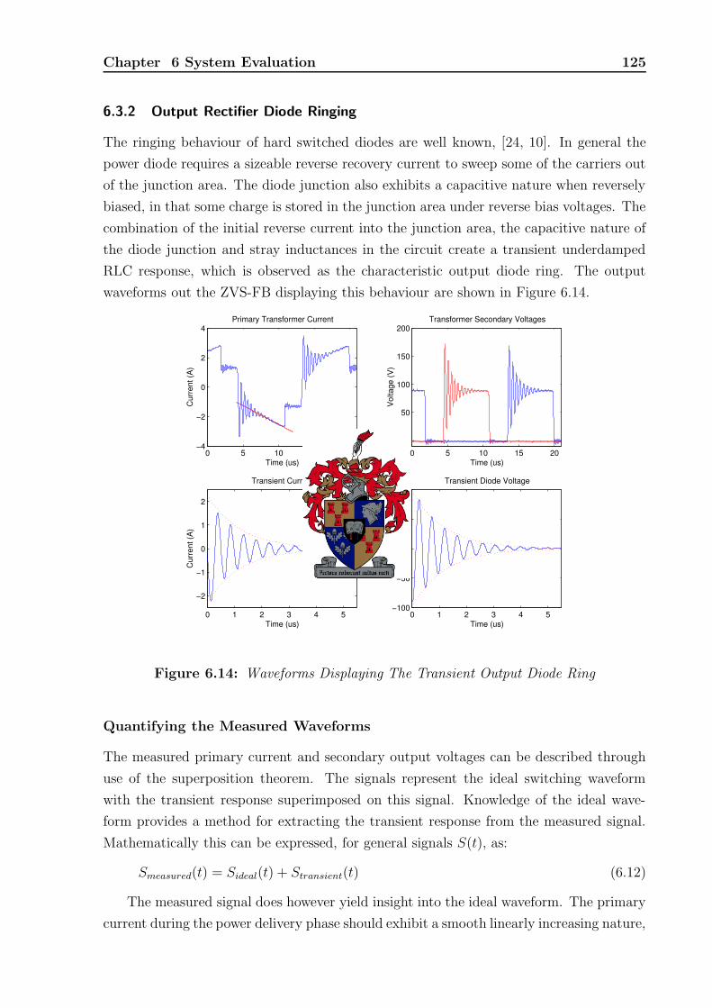
Chapter 6 System Evaluation 125
6.3.2 Output Rectifier Diode Ringing
The ringing behaviour of hard switched diodes are well known, [24, 10]. In general the
power diode requires a sizeable reverse recovery current to sweep some of the carriers out
of the junction area. The diode junction also exhibits a capacitive nature when reversely
biased, in that some charge is stored in the junction area under reverse bias voltages. The
combination of the initial reverse current into the junction area, the capacitive nature of
the diode junction and stray inductances in the circuit create a transient underdamped
RLC response, which is observed as the characteristic output diode ring. The output
waveforms out the ZVS-FB displaying this behaviour are shown in Figure 6.14.
0 5 10 15 20−4
−2
0
2
4
Time (us)
Cur
rent
(A)
Primary Transformer Current
0 5 10 15 20
0
50
100
150
200
Time (us)
Vol
tage
(V)
Transformer Secondary Voltages
0 1 2 3 4 5
−2
−1
0
1
2
Time (us)
Cur
rent
(A)
Transient Current
0 1 2 3 4 5−100
−50
0
50
100
Time (us)
Vol
tage
(V)
Transient Diode Voltage
Figure 6.14: Waveforms Displaying The Transient Output Diode Ring
Quantifying the Measured Waveforms
The measured primary current and secondary output voltages can be described through
use of the superposition theorem. The signals represent the ideal switching waveform
with the transient response superimposed on this signal. Knowledge of the ideal wave-
form provides a method for extracting the transient response from the measured signal.
Mathematically this can be expressed, for general signals S(t), as:
Smeasured(t) = Sideal(t) + Stransient(t) (6.12)
The measured signal does however yield insight into the ideal waveform. The primary
current during the power delivery phase should exhibit a smooth linearly increasing nature,

Chapter 6 System Evaluation 126
governed by the input and output voltages and the output filter inductance. Thus the
ideal waveform can be extracted from the measured waveform by fitting a straight line to
the measured data in the applicable time window. The process is shown by the red line
superimposed on the measured current signal in Figure 6.14. By applying this method
to both the current and voltage signals and using equation 6.12 the transient waveforms
displayed in Figure 6.14 are obtained.
The equivalent circuit describing the ringing circuit consists of an inductor, capacitor
and a resistor in series with initial current stored in the inductor. This circuit is similar
to the circuit described in section 3.4.2. The voltage across the equivalent capacitor and
the inductor current can be described by,
I(t) = e(−αt) B1 cos(ωt) + B2 sin(ωt) (6.13)
V (t) = −e−αt
αB1 cos(ωt) − ωB1 sin(ωt) + ωB2 cos(ωt) + αB2 sin(ωt)
C (α2 + ω2)
(6.14)
with the parameters α, ω, B1 and B2 as defined in equations 3.11, 3.12, 3.14 and 3.15.
The resonant frequency is measured as 2 MHz. The effective inductance in the reso-
nant circuit is the transformer leakage inductance referred to the secondary, or LL = 20.29
µH. From equation 3.11 the effective capacitance is calculated to be in the order of 340
pF. The effective capacitance in the ringing circuit would be the diode body capacitance
in parallel with the transformer secondary winding capacitances. The effective diode
body capacitance over the applicable voltage range is estimated from the manufacturer
datasheet as 100 pF. Thus the the total secondary interwinding capacitance is estimated
at 240 pF.
From equation 6.13 it is clear that the ringing waveforms is bounded by the normalised
envelope described by E(t) = ±e−αt. The value of α is estimated by taking the natural
logarithm of the normalised local maxima corresponding to the peaks of the unaltered
sinusiod. From the estimated value of α and equation 3.12 the effective resistance is
estimated at 30.7 Ω. This resistance is significantly higher than the designed winding
resistance of 100 mΩ but this increase is attributed to the significant role of the skin
effect at a frequency of 2 MHz.
The damping ratio of the circuit is expressed by the factor ζ, a number between 0
and 1 where 0 implies a totally undamped circuit and 1√2
critically damped [11]. With
reference to equation 6.13 the damping ratio is defined as;
ζ =α
ω(6.15)
The measured waveforms of Figure 6.14 corresponds to a damping ratio ζ = 0.066.

Chapter 6 System Evaluation 127
Designing the Output Snubber
The output diode ring can be controlled through the addition of a dissipative snubber on
the output. Some work have also been done in using an alternative synchronous rectifica-
tion technique to achieve soft-switching on the secondary side with resultant elimination
of the output diode ring [53, 25, 36].
Assuming the effective wiring resistance is much larger than the ESR of the parasitic
diode capacitance, the equivalent small-signal circuit of the circuit parasitics with an
added dissipative snubber is shown in Figure 6.15, where C, R and L denotes the circuit
parasitics and Cs and Rs are the added snubber capacitor and damping resistor.L R
C
Rs
Cs
Figure 6.15: Equivalent Parasitics and Snubber Circuit
The first constraint in the design is the dissipative nature of the snubber. The power
loss in the damping resistor can be approximated as;
Ps = CsV2busfs (6.16)
If the power loss in the snubber circuits, one on each rectifier diode, are limited to 1 % of
the power output capacity of the system, the snubber capacitances must be smaller than
470 pF.
With reference to figure 6.15 the transfer function of the voltage across the snubber-
diode combination as a function of the current in the inductor can be given as:
H(s) =V (s)
I(s)=
sRsCs + 1
s3LCCsRs + s2 L(C + Cs) + CCsRRs + sR(C + cs) + 1(6.17)
The denominator corresponds to three roots of which, in general for applicable values, one
would be real and the remaining two would be complex. Choosing a range of capacitances
from 100 pF to 500 pF and damping resistances from 10 Ω to 1.6 kΩ the plot of damping
ratio versus snubber component values in Figure 6.16 is obtained. It is clear that superior
damping occurs at higher capacitance values, but this damping would result in higher
dissipation.
Taking a two dimensional slice from Figure 6.16 at a capacitance value of 470 pF
the optimal damping resistance can be obtained. The damping ratio as a function of

Chapter 6 System Evaluation 128
0 200 400 600 800 1000 1200 1400 16000
200
400
600
0.05
0.1
0.15
0.2
0.25
0.3
0.35
0.4
Resistance (Ohm)
Capacitance (pF)
Dam
ping
Rat
io
Figure 6.16: Damping Ratio Versus Snubber Component Values
damping resistance with a snubber capacitance of 470 pF is shown in Figure 6.17. The
optimal value of damping is found to be 0.38 occurring at Rs = 302 Ω. The normalised
voltage response to a current step input, i.e. reverse recovery current, with and without
the snubber is shown in Figure 6.18.
6.3.3 Verification of the Parasitics Measurements
Precise knowledge of the transformer leakage inductance and the inter winding capaci-
tance is important in analysing the converter behaviour. In the preceding sections the
transformer leakage inductance was calculated from a modified short circuit test proce-
dure as 4.61 µH. The inter winding capacitance was calculated from an analysis of the
output diode ringing waveforms as 240 pF.
These two measurements can be verified by investigating the resonant energy transfer
during phase shifted operation on the primary side of the transformer. From section 3.4
the half-leg voltage will change resonantly with a sinusoidal shape. In short the amplitude
of this sinusoid is determined by the current magnitude stored in the leakage inductance
at the initiation of this energy transfer phase while the frequency is determined by the
magnitude of the leakage inductance and the combined capacitances. During the energy
transfer cycle the two half-leg switch output capacitances are effectively in parallel with
the transformer winding capacitance. Therefore the effective capacitance can be given as:
C = 2Coss + Cxmr (6.18)
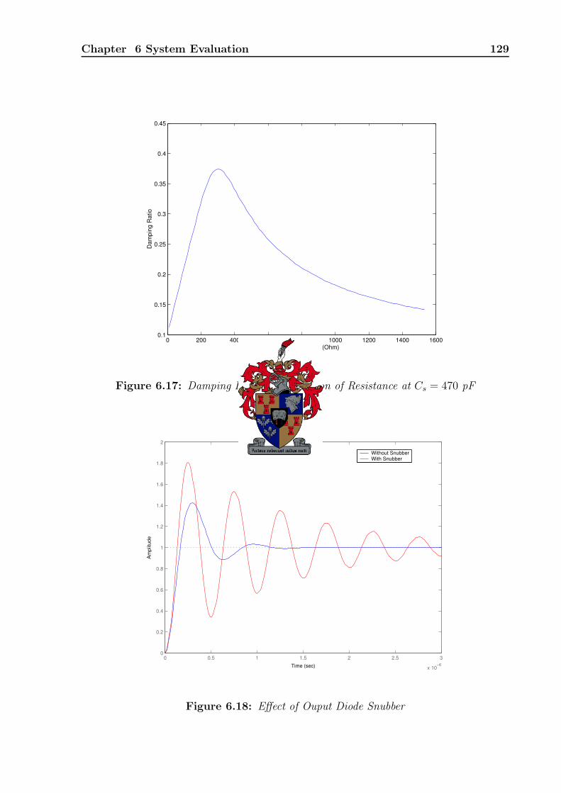
Chapter 6 System Evaluation 129
0 200 400 600 800 1000 1200 1400 16000.1
0.15
0.2
0.25
0.3
0.35
0.4
0.45
Damping Resistance (Ohm)
Dam
ping
Rat
io
Figure 6.17: Damping Ratio as a Function of Resistance at Cs = 470 pF
Time (sec)
Am
plitu
de
0 0.5 1 1.5 2 2.5 3
x 10−6
0
0.2
0.4
0.6
0.8
1
1.2
1.4
1.6
1.8
2
Without SnubberWith Snubber
Figure 6.18: Effect of Ouput Diode Snubber

Chapter 6 System Evaluation 130
−2 −1 0 1 2 3 4−50
0
50
100
150
200
250
300
350
400
time (µ s)
Hal
f−Le
g V
olta
ge (V
)
Figure 6.19: Incomplete Energy Transfer Half-Leg Voltage Waveform
The resonant frequency of the energy transition can be calculated as,
ω =1√LLC
(6.19)
A waveform of the half leg voltage under incomplete energy transition is displayed in
Figure 6.19. The resonant half-sinusoidal voltage ring is clearly visible. A zoomed image
of the measured voltage waveform with a calculated sinusoid superimposed is included
in Figure 6.20. Due to uncertainties concerning the work point of the converter and
switching information the sinusoid was fitted to the data in both magnitude and phase.
It is clear that the measured resonant ring frequency and the frequency calculated
from the parasitics are comparable. To this end, the measured values are verified.
6.3.4 Output Step Response
The output step response of the converter was measured in the following manner. The
converter was given a constant current command while the output was open circuited.
The open circuited output prevents the flow of current and hence the output voltage is
at a maximum. A load was then switched into the circuit. The load, a kettle, can be
regarded as a constant resistive load of approximately 25 Ω.

Chapter 6 System Evaluation 131
0 20 40 60 80 100 120 140 160 180 2000
20
40
60
80
100
120
140
160
180
200
time (nS)
Hal
f−Le
g V
olta
ge (V
)
Measured Ring VoltagePredicted Ring Voltage
Figure 6.20: Measured Voltage Ring versus Calculated Response
The output current and voltage waveforms of the converter under step response con-
ditions are shown in Figures 6.21 and 6.22.
6.3.5 General Tests and Plasma Loads
The converter was analysed for stability at various operational points. The converter
work point was adjusted through manipulation of the load, input voltage and current
command. The converter operated satisfactory.
A plasma load was created in the following way. An output current was facilitated, in
a manner similar to the step response measurement. However, after load current initiation
the anode was separated slightly from the load. The output inductance supplies the energy
to ionize the air gap between the anode and load and a plasma occurs between the anode
and the load.
The converter was able to sustain the plasma in free air at various plasma lengths
and output current settings.
The failure mode, described in section 4.1.1, was however found during the plasma
initiation tests. Traditional methods of plasma initiation would have the cathode and
anode short circuited to facilitate a load current, after which the cathode and anode
would be separated from one another. However, this operation resulted, at times in the
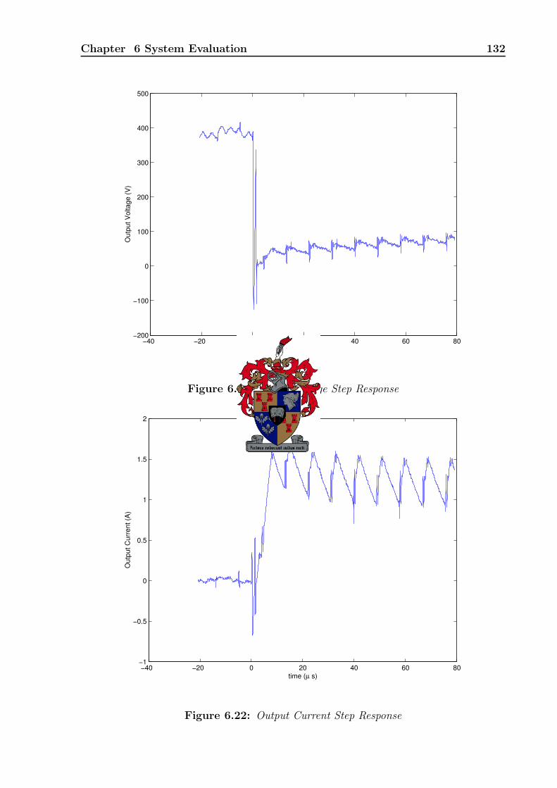
Chapter 6 System Evaluation 132
−40 −20 0 20 40 60 80−200
−100
0
100
200
300
400
500
time (µ s)
Out
put V
olta
ge (V
)
Figure 6.21: Ouput Voltage Step Response
−40 −20 0 20 40 60 80−1
−0.5
0
0.5
1
1.5
2
time (µ s)
Out
put C
urre
nt (A
)
Figure 6.22: Output Current Step Response
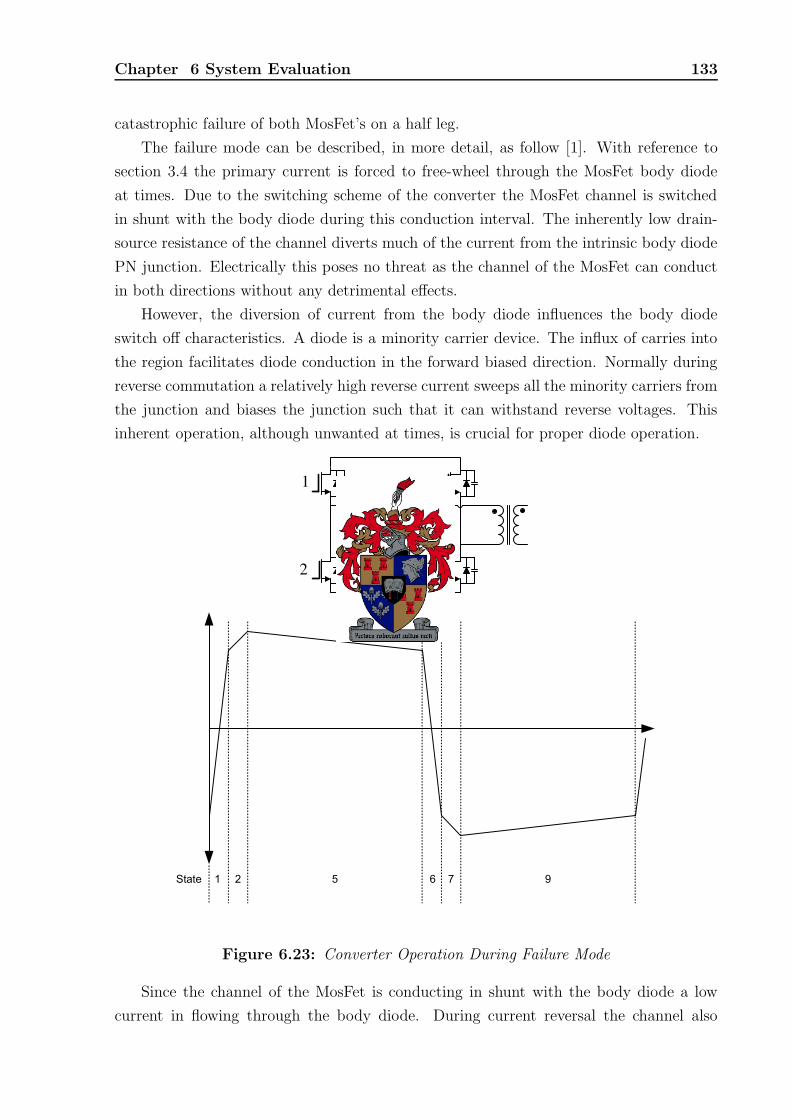
Chapter 6 System Evaluation 133
catastrophic failure of both MosFet’s on a half leg.
The failure mode can be described, in more detail, as follow [1]. With reference to
section 3.4 the primary current is forced to free-wheel through the MosFet body diode
at times. Due to the switching scheme of the converter the MosFet channel is switched
in shunt with the body diode during this conduction interval. The inherently low drain-
source resistance of the channel diverts much of the current from the intrinsic body diode
PN junction. Electrically this poses no threat as the channel of the MosFet can conduct
in both directions without any detrimental effects.
However, the diversion of current from the body diode influences the body diode
switch off characteristics. A diode is a minority carrier device. The influx of carries into
the region facilitates diode conduction in the forward biased direction. Normally during
reverse commutation a relatively high reverse current sweeps all the minority carriers from
the junction and biases the junction such that it can withstand reverse voltages. This
inherent operation, although unwanted at times, is crucial for proper diode operation.
1
2
3
4
Figure 6.23: Converter Operation During Failure Mode
Since the channel of the MosFet is conducting in shunt with the body diode a low
current in flowing through the body diode. During current reversal the channel also

Chapter 6 System Evaluation 134
carries the brunt of the current with the result that the ensuing reverse current through
the diode junction is low. The conducting junction also clamps the reverse voltage the
diode has to withstand to the conducting channel voltage, which due to the low drain-
source resistance will be low. Since the diode is switched off under the described ‘soft’
conditions and the reverse recovery current is low, many minority carriers remain in the
junction after current commutation. The low reverse voltage applied to the junction
implies that the body diode junction is effectively in limbo, with no reverse current to
sweep the carriers from the junction.
The remaining carriers in the channel will recombine as time passes. As this natural
recombination takes place the junction will again be completely free of minority carriers
and can block the rated reverse voltage without problems.
However, if the effective duty-cycle of the converter is short, as it will be when driving
a low ohmic load, the time allocated, with reference to Figure 6.23, to State 4 will be long.
This implies that the body diode of switch 3 will conduct for the whole time period. When
the current reverses, during State 6 the body channel of switch 3 is conducting in shunt
with the body diode, with the result that some carriers remain in the diode junction.
If the time allocated to State 7 is short, i.e. the current rise time is short and the
peak current value is reached in a short time span (as will happen under short circuit
conditions), insufficient time might be allocated for the natural recombination of the
minority carriers in the body diode of switch 3. This implies that when switch 3 is
switched off at the end of State 7 some minority carriers might remain in the body diode
junction.
If enough carriers remain in the junction and the ensuing voltage and current rise
times are fast enough the resulting reverse recovery current might be sufficient to cause
second breakdown in the NPN structure of the power MosFet. As soon as the second
breakdown occurs switches 3 and 4 are effectively cross-conducting and shorting the input
bridge voltage. This unwanted conduction mode results in severe over currents and in the
resulting destruction of both switch devices.
Although the author has been aware of this failure mechanism, some of the litera-
ture considered [1] implied that FREDFET’s, Fast Recovery Body-Diode MosFet, have
a sufficiently low minority charge remaining in the junction to prevent this failure mode.
However, the severe load requirements of the plasma load demands such short effective
duty cycles that the FREDFET topology MosFets are also subject to this failure mode.
To circumvent this problem a series resistance is placed in the output circuit, such
that the circuit will never be subject to short circuit conditions. This implies that the
effective duty-cycle will be long enough to allow for the natural recombination of the the
minority carriers.
At the time of writing this report, the opportunity has not arisen to test the supply

Chapter 6 System Evaluation 135
with a contained plasma. Although an appointment has been made. However, it is
the opinion of the author, after testing the converter at several work points with an
uncontained plasma arc without problems, that the converter is able to establish and
maintain a contained plasma arc. This observation is further supported in that plasma
loads in open air are much more volatile that their contained counterparts.

Chapter 7Conclusion
“I do not think there is any thrill that can go through the human heart like that felt by
the inventor as he sees some creation of the brain unfolding to success... Such emotions
make a man forget food, sleep, friends, love, everything.”
Nikola Tesla
This, final, chapter comments of the work presented in this thesis. This discussion will
comment on the contributions of this study, the conclusions of the project and will
finally highlight areas for future study.
7.1 Summary of Study
The study was aimed at investigating and proposing a switched mode converter for plasma
applications. To that end the specific demands of the plasma as load was investigated to
quantify the requirements of the proposed converter. The use of high frequency converters
was then contrasted with the use of line frequency topologies, after which a investigation
of different high frequency topologies followed. The ZVS-FB with CDR was selected as
the topology of choice. The ZVS-FB operation was analysed and a 3 kW prototype was
designed and built. A PFC boost rectifier front stage was included in the system, to allow
operation from a residential outlet.
Several control strategies was considered for the converter, with PCMC as the strategy
of choice. A new model for the Full-Bridge converter with a Current Doubling Rectifier
under PCMC was developed. Finally the converter operation was investigated and veri-
fied.
7.1.1 Main Contributions
The main contributions of this study are:
• The investigation into the plasma as load. This included the operation of the plasma
136

Chapter 7 Conclusion 137
arc, inclusive of the electrical and mechanical properties. The specific demands the
plasma placed on the power supply was investigated. Finally an electrical model of
the plasma as electrical load was derived.
• The inherent advantages of high frequency power conversion was contrasted with the
prevailing line frequency technologies. This aspect of the study, although not novel,
is highlighted as this was the primary problem statement of Thermtron, NECSA
and the DASC Consortium who funded this project.
• The complete investigation of the zero voltage switched full-bridge with a current
doubling rectifier.
• The small-signal analysis of the converter under peak current mode control. The
prior art of peak current mode control representation in the averaged, continuous
time domain was repeated and accepted. A proposed model for the converter was
investigated and after an in depth analysis an improved model for the converter was
proposed.
• A novel method was developed to characterise the parasitic elements of the high
frequency transformer.
• An operational converter, able to sustain a arc in open air, at various arc-current
values and arc lengths.
7.2 Conclusions
Regarding the original problem statement of: ‘are high frequency power conversion topolo-
gies suited for applications in the plasma industry?’ The study concluded that high fre-
quency topologies have several advantages over the prevalent line frequency topologies.
As the power handling capabilities of switching devices such as IGBT’s improve, the
traditional niche of thyristor controlled converters in plasma processing will shrink to
converters of very high power ratings, such as arc furnaces.
Although the delivered prototype requires several improvements the proposed con-
verter meets the requirements of the project. The peak current mode control topology
also ensures that the proposed converter can be paralleled to meet higher current re-
quirements. This capability is instrumental in fulfilling the fundamental problem of the
project initiators; high frequency power conversion in the medium to high power plasma
processing industry. The conclusion of this study to that end is that high frequency would
be the natural next step for the industry in South Africa. Although the design and im-
plementation of this technology would be expensive and labour intensive, the advantages
of high frequency converters over line frequency technology warrants this investment.

Chapter 7 Conclusion 138
7.3 Further Work
During the study several areas deserving of further investigation has been identified. These
areas can be summarised as:
• Extension of the study to a higher power level of 75 kW. Although a concept design
of a 75 kW system and the expansion of the control board to include a high power
capability was included in this study, this converter never realised, due to external
influences. The higher power converter would be able to power a direct current
linear plasma torch in a pilot study. The higher power level also provides a good
comparison point for a high and line frequency converter. At a power level of 75 kW
the converters can operated side by side and compared, with the results extrapolate-
able to higher power levels.
• Investigation into a topology where the isolation barrier is provided by a line fre-
quency transformer. Although this transformer will be large and bulky the ex-
pansion of high frequency isolation transformers into high (more than 100 kW)
power levels remains problematic. Alternatively this study might be expanded into
a thorough investigation into the realisation of high frequency power transformers
to higher power levels.
• Expansion of the FFT method of determining the parameters of the high frequency
transformer to other isolated topologies.
• Updating the proposed converter with all the circuit modifications. This industri-
alisation phase must include other modifications such as the change from MosFet
power switches to IGBT’s.

Bibliography
[1] AIGNER, H., DIERBERGER, K., and GRAFHAM, D., “Improving Phase-Shift
ZVT Converter for Failure-free Operation Under Extreme Conditions in Welding and
Similar Applications.” 33rd IEEE Industry Applications Society Conference, 1998.
[2] BALOGH, L., “The Current-Doubler Rectifier: An Alternative Rectification Tech-
nique for Push-Pull and Bridge Converters.” Design Note DN-63, Unitrode div. of
Texas Instruments, 1991.
[3] BALOGH, L., “Unitrode - UC3854A/B and UC3855A/B Provide Power Limiting
With Sinusoidal Input Current for PFC Front Ends.” Design Note DN-66, Unitrode
div. of Texas Instruments, 1999.
[4] BILAU, T. Z., MEGYERI, T., SARHEGYI, A., MARKUS, J., and KOLLAR, I.,
“Four Parameter Fitting of Sine Wave Testing Results: Iteration and Convergence.”
Fourth International Conference on Advanced A/D and D/A Conversion Techniques
and their Applications, June 26-28 2002, Prague.
[5] BILL, B., WALD, S., KIMCHI, D., and KAPLAN, Z., “Experimental Demonstration
and Simulation of a Dual-Stage Solid Propellant Gun Concept.” Journal of Propul-
sion and Power, 1994, Vol. 10, No. 2, No. 2, pp. 279–285.
[6] BOLEY, F. I., Plasmas - Laboratory and Cosmic. First edition. Princeton, New
Jersey: D. van Nostrand company, inc., 1966.
[7] CHALMERS, I., BAIRD, R., and KELLY, T., “Control of an ozone generator - theory
and practice.” Measurement Science and Technology, 1998, Vol. 9, pp. 983–988.
[8] CHEN, W., LEE, F., JOVANOVIC, M., and SABATE, J., “A Comparative Study
of a Class of Full-Bridge Zero-Voltage-Switched PWM Converters.” Tenth Applied
Power Electronic Conference and Exposition, 5-9 March 1995, Vol. 2, pp. 893–899.
[9] DIXON, L., “Average Current Mode Control of Switching Power Supplies.” Appli-
cation Note U-140, Unitrode div. of Texas Instruments, 1990.
139

BIBLIOGRAPHY 140
[10] ERICKSON, R. W. and MAKSIMOVIC, Fundamentals of Power Electronics. Sec-
ond edition. Norwell, Massachusetts: Kluwer Academic Publishers, 2001.
[11] FRANKLIN, G., POWELL, J., and EMAMI-NAEINI, A., Feedback Control of Dy-
namic Systems. Third edition. Reading, Massachusetts: Addison-Wesley Publishing
Company, 1994.
[12] GODYAK, V., “Radio Frequency Light Sources.” 35th IEEE Industry Applications
Conference, 2000.
[13] Institute of Thermophysics, “Electro-Arc Heaters and Plasma Technologies.” tech.
rep., Russian Academy of Sciences, Siberian Branch.
[14] JONES, R., DENTON, G., REYNOLDS, Q., et al., “Recovery of Cobalt from Slag
in a DC Arc Furnace at Chambishi, Zambia.” Journal of the South African Institute
of Mining and Metallurgy, 2002, Vol. 102, No. 1, No. 1, pp. 5–9.
[15] KAZIMIERCZUK, M., “Transfer Function of Current Modulator in PWM Convert-
ers with Current Mode Control.” IEEE Transactions on Circuits and Systems - I:
Fundamental Theory and Applications, 2000, Vol. 47, No. 9, No. 9, pp. 1407–1412.
[16] KORZEKWA, R. et al., “Experimental Results Comparing Pulsed Corona and Di-
electric Barrier Discharges for Pollution Control.” 11th IEEE International Pulsed
Power Conference, 1997.
[17] KUO, S., BIVOLARU, D., LAI, H., and LAI, W., “Plasma Torch Igniters for a
Scramjet Combustor.” 42nd AIAA Aerospace Sciences Meeting and Exhibit, 5 - 8
January 2004, Reno, Nevada.
[18] KUTKUT, D., “An Improved Zero-Voltage Switching PWM Converter Using a Two
Inductor Rectifier.” IEEE Transactions on Industry Applications, January 1995,
Vol. 31, No. 1, No. 1, pp. 119–126.
[19] KUTKUT, N. H. and LUCKJIFF, G., “Current Mode Control of a Full-Bridge DC-
to-DC Converter with a Two Inductor Rectifier.” Proceedings of the 28th Annual
IEEE Power Electronic Specialist Conference, June 1997, Vol. 1, pp. 203–209.
[20] LIVESCU, C. D., “Current doubler topology: Myth and reality.” available online:
http://www.powersupplies.net/knowledge/idoubler/idoubler.htm.
[21] MAMMANO, R., “Switching Power Supply Topology; Voltage Mode vs. Current
Mode.” Design Note DN-62, Unitrode div. of Texas Instruments, 1990.

BIBLIOGRAPHY 141
[22] MENTEL, J., LUHMANN, J., and NANDELSTADT, D., “Experimental Investiga-
tion of Electrodes for High Pressure Discharge lamps.” 35th IEEE Industry Applica-
tions Conference, 2000.
[23] MIDDLEBROOK, R. and CUK, S., “A General Unified Approach to Modelling
Switching Converter Stages.” 1976 IEEE Power Electronic Specialist Conference
Record, 1976.
[24] MOHAN, N., UNDERLAND, T. M., and ROBBINS, W. P., Power Electronics; Con-
verters, Applications and Design. Second edition. New York: John Wiley & sons
inc., 1995.
[25] MORIMOTO, T., SAITOU, K., SHIRAKAWA, S., and NAKAOKA, M., “Trans-
former Parasitic Reactive Components-Assisted Soft-Switching PWM Inverter Type
DC-DC Converter with ZCS Power Switches.” 31st IEEE Power Electronic Specialist
Conference, 2000.
[26] NILSSON, J. W. and RIEDEL, S. A., Electric Circuits. Fifth edition. Reading,
Massachusetts: Addison-Wesley Publishing Company, 1996.
[27] OKUBO, M., KUROKI, T., KAMATEKA, H., and YAMAMOTO, T., “Odor Con-
trol using the AC Barrier Type Plasma Reactors.” 35th IEEE Industry Applications
Conference, 2000.
[28] PALMER, S. B., “St. elmo’s fire.” available online:
http://www.mysterylights.com/types/stelmo.
[29] PENETRANTE, B., “Pollution Control Applications of Pulsed Power Technology.”
9th IEEE Pulsed Power Conference, 1993.
[30] PETKOV, R., “Optimal Design of a High-Power High-Frequency Transformer.”
IEEE Transactions on Power Electronics, January 1996, Vol. 11, No. 1, No. 1, pp. 33–
42.
[31] PRIETO, R., GARCIA, O., COBOS, J., and UCEDA, J., “Designing Inductors at
Device and Converter Level.” IEEE International Symposium on Industrial Electron-
ics, 2002, Vol. III, pp. 987–993.
[32] PROAKIS, J. A. and MANOLAKIS, D. G., Digital Signal Processing; Principles,
Algorithms and Applications. Third edition. London: Prentice Hall International
Editions, 1996.

BIBLIOGRAPHY 142
[33] RAJAGOPALAN, J., XING, K., GUO, Y., and LEE, F., “Modeling an Dynamic
Analysis of Paralleled dc/dc Converters with Master-Slave Current Sharing Control.”
IEEE APEC Conference Record, 1996, pp. 678–684.
[34] RIDLEY, R., “A New, Continuous-Time Model For Current-Mode Control.” IEEE
Transactions on Power Electronics, 1991, Vol. 6, No. 2, No. 2, pp. 271–280.
[35] ROOS, S. D., “Skakelmodus kragbron vir plasma toepassings.” Master’s thesis,
Randse Afrikaanse Universiteit, 1997.
[36] RUKONUZZAMAN, M., AL, M. A., NAKAMURA, M., MOISSEEV, S., and
NAKAOKA, M., “Transformer Parasitic Circuit Parameter-Assisted Soft-Switching
DC-DC Power Converter with Secondary Side Synchronous Phase-Shifted Active
Rectifier.” 31st IEEE Power Electronic Specialist Conference, 2000.
[37] RUKONUZZAMAN, M., AL, M., NAKAMURA, M., MOISSEEV, S., and
M.NAKAOKA, “Transformer Parasitic Circuit Parameter Assisted Soft Switching
DC-DC Power Converter with Secondary Side Phase Shifted Active Rectifier.” 31st
IEE Power Electronic Specialist Conference, 2000.
[38] SABATE, J., FARRINGTON, R., JOVANOVIC, M., and LEE, F., “Effect of
FET Output Capacitance on ZVS of Resonant Converters.” IEEE Transactions on
Aerospace and Electronic Systems, January 1996, Vol. 32, No. 1, No. 1, pp. 255–266.
[39] SABATE, J., VLATKOVIC, V., RIDLEY, R., and LEE, F., “High Voltage, High
Power, ZVS, Full-Bridge PWM Converter Employing an Active Snubber.” Sixth
American Power Electronic Conference, 10-15 March 1991, pp. 158–163.
[40] SCHMITT, P. and GERSTER, C., “Optimised Pulse Modulation for Plasma Power
Supply.” 10th European Conference on Power Electronics and Applications, 2001.
[41] SCIANI, V. and MA, T., “High Current Choppers in the Metals Industry.” Confer-
ence Record of the IEEE Industry Applications Conference, 2000.
[42] SEVERNS, R., “Circuit Reinvention in Power Electronics and Identification of Prior
Work.” IEEE Transactions on Power Electronics, January 2001, Vol. 16, No. 1.
[43] STURROCK, P. A., Plasma Physics. First edition. Cambridge: University Press,
1994.
[44] SULLIVAN, C. R., “Optimal Choice for Number of Strands in a Litz-Wire Trans-
former Winding.” IEEE Transactions on Power Electronics, March 1999, Vol. 14,
No. 2, No. 2, pp. 283–291.

BIBLIOGRAPHY 143
[45] SUN, J. and RAJASEKRAN, V., “DCM Analysis and Modeling of Half-Bridge Con-
verters with Current-Doubler Rectifier.” 32nd Power Electronic Specialist Confer-
ence, 2001.
[46] THERON, P. and FERREIRA, J., “The Partial Series Resonant Converter: a New
Zero Voltage Switching dc to dc Converter.” Transactions of the South African In-
stitute of Electrical Engineers, March 1994, pp. 18–23.
[47] TODD, P. C., “UC3854 Controlled Power Factor Correction Circuit Design.” Appli-
cation Note U-134, Unitrode div. of Texas Instruments, 1997.
[48] VAJTA, M., “Some Remarks on Pade Approximations.” 3rd TEMPUS-INTCOM
Symposium, Veszprem, Hungary, 9-14 September 2000.
[49] VAN HEESCH, E. et al., “Pulsed Corona for Gas and Water Treatment.” 11th IEEE
International Pulsed Power Conference, 1997.
[50] VARDA, “St. elmo’s fire - folklore and myth.” available online:
http://www.geocities.com/varda valar/S.htm.
[51] VORPERIAN, V., “Simplified Analysis of PWM Converters Using Model of PWM
Switch Part I: Continuous Conduction Mode.” IEEE Transactions on Aerospace and
Electronic Systems, 1990, Vol. 26, No. 3, No. 3.
[52] VORPERIAN, V., “Simplified Analysis of PWM Converters Using Model of PWM
Switch Part II: Discontinuous Conduction Mode.” IEEE Transactions on Aerospace
and Electronic Systems, 1990, Vol. 26, No. 3, No. 3.
[53] WATSON, R. and LEE, F. C., “Analysis, Design and Experimental Results of a 1-
kW ZVS-FB-PWM Converter Employing Magamp Secondary-Side Control.” IEEE
Transactions on Industrial Electronics, October 1998, Vol. 45, No. 5.
[54] WU, T., CHEN, C., and HSU, W., “Design and Development of Driving Waveforms
for AC PDP’s.” 37th IEEE Industry Applications Conference, 2002.
[55] YAN, K., VAN HEESCH, E., et al., “A 2.0kW Pulsed Corona System for Inducing
Chemical Reactions.” 35th IEEE Industry Applications Conference, 2000.
[56] YOUNG, H. D. and FREEDMAN, R. A., University Physics with Modern Physics.
Tenth edition. San Fransisco: Addison-Wesley Publishing Company, 2000.
[57] ZHUKOV, M., “Linear Direct Current Plasma Torches.” Thermal Plasma and New
Materials Technology, Published by Cambridge Interscience Publishing, 1994, pp. 9–
43.

Appendix AMathematical Derivations
The following conventions is used throughout this appendix.
Nomenclature
Matrices and vectors are represented by boldface identifiers, e.g. A1, C
R Magnetic Reluctance
φ Magnetic Flux
Ae Equivalent Core Area
le Equivalent Core Length
µ0 Permeability of free space, 4π × 10−7
µr Relative Permeability, in general including effect of airgap
Averaging
x1(t)Tsdenotes the average value of x1(t) over the switching interval Ts, or mathemati-
cally:
x1(t)Ts=
1
Ts
∫ t+Ts
t
x1(τ)dτ (A.1)
Assumptions
All perturbations is much smaller than the nominal values, id est
X1 x1(t) (A.2)
144

Appendix A Mathematical Derivations 145
Switch Network
+
_
+
_
) ( 1 t V ) ( 2 t V
) ( 1 t I ) ( 2 t I
) ( t out V ) ( t dc V
+
_
Figure A.1: Buck Converter with Average Switch Network
A.1 Averaged Switch Network for Buck Converter
With reference to figures A.1 and A.2 the following equations follow, assuming that the
V1 and I2 are independent quantities:
i1(t)Ts= d(t)i2(t)Ts
(A.3)
v2(t)Ts= d(t)v1(t)Ts
The equalities describing the system can be perturbed;
d(t) = D + d(t)
i1(t)Ts= I1 + i1(t)
i2(t)Ts= I2 + i2(t) (A.4)
v1(t)Ts= V1 + v1(t)
v2(t)Ts= V2 + v2(t)
Substitution of equation A.4 into A.3 yields:
I1 + i1(t) = D(I2 + i2(t)) + dI2 + di2(t)︸ ︷︷ ︸
=0
V2 + v2(t) = D(V1 + v1(t)) + dV1 + dv1(t)︸ ︷︷ ︸
=0
(A.5)

Appendix A Mathematical Derivations 146
t
) ( 2 ), ( 1 t i t i
s dT s T ) 1 ( d s T 0
Average of i 1 (t)
Average of i 2 (t)
t
) ( 2 ), ( 1 t v t v
s dT s T ) 1 ( d s T 0
Average of v 2 (t)
Average of v 1 (t)
i 1 (t)
i 2 (t)
Figure A.2: Typical Waveforms of the Buck Converter
The non-linear products of time varying signals, collected on the righthandside can
be equated to zero provided that assumption A.2 holds. Further investigation of A.5
shows that the current in port 1 can be described as a superposition of two sources,
D(I2 + i2(t)) and dI2. The second source is driven by the control input perturbation
d and can be regarded as an independent current source. The first source is however
dependent on the independent current in port 2, I2 + i2(t), and can be regarded as a
dependent current source. Investigation of the equation governing the voltage of port 2,
shows both a dependent and an independent voltage source.
The two independent sources both display a dependency on the independent quantity
of the other port, with the same dependence constant, D. This dependency is encountered
in the normal operation of a transformer, where the output voltage is dependent upon
the input voltage and the input current upon the output current, all with the common
constant a defined as N1
N2. Extension of the transformer model into the dc domain yields
the equivalent circuit for the Buck average switch as shown in Figure A.3

Appendix A Mathematical Derivations 147
−+
+)(1
~1 tvV
)(1~
1 tiI +
)(2~
2 tiID +2~Id +
_ )(1~
1 tvVD +
1~Vd )(2
~2 tiI +
−+
+)(2
~2 tvV
(a)
2~Id
1~Vd1I
−
+
1V
−
+
2V
2I
(b)
D:1
Figure A.3: Equivalent Switch Model for Buck Converter; (a) equivalent two port (b)
Equivalence with extended transformer model
A.2 State Space Averaging of the Current Doubler
The full-bridge converter can be approximated by two Buck regulators operating in par-
allel. If the non-ideal components of the magnetic transformer are ignored and the turns
ratio taken as 1:1, the full-bridge current doubler combination can be approximated by
the sub-circuits shown. Three modes of operation can be identified. Inspection of the op-
eration of the topology reveals that Mode I will occur sandwiched between each transition
from Mode II to Mode III or vice versa, thus Mode I will occur at twice the frequency of
Modes II and III.
Mode I
Mode 1 can be identified as the free-flowing mode where no external source is connected
to the sub-circuit and the system operation relies on energy stored in the two inductors
and the capacitor. The following relationships follow:
The output voltage:
Vout = x3 + Crcx3 (A.6)

Appendix A Mathematical Derivations 148
and the interdependent relationships:
L1x1 + rl1x1 + x3 + Crcx3 = 0
L2x2 + rl2x2 + x3 + Crcx3 = 0 (A.7)
x1 + x2 −x3 + Crcx3
R= Cx3
Manipulation and substitution of A.6 yields
x1 = −x1
Rrl1 + Rrc + rl1rc
(R + rc) L1− x2
Rrc
(R + rc)L1− x3
R
(R + rc)L1
x2 = −x1
Rrc
(R + rc)L2− x2
Rrl2 + Rrc + rl2Rc
(R + rc)L2− x3
R
(R + rc)L2(A.8)
x3 = x1
R
(R + rc) C+ x2
R
(R + rc)C− x3
1
(R + rc)C
Mode II
Mode II is characterized by the energy storage in L1 and energy extraction from L2. The
network formed by the switches, L1 and the load takes the form of a Buck converter with
the addition of the energy stored in L2. Inspection reveals:
Vin = L1x1 + rl1x1 + x3 + Crcx3
0 = L2x2 + rl2x2 + x3 + Crcx3 (A.9)
x1 + x2 −x3 + Crcx3
R= Cx3
and through manipulation
x1 =Vin
L1
− x1
Rrl1 + Rrc + rl1rc
(R + rc) L1
− x2
Rrc
(R + rc)L1
− x3
R
(R + rc)L1
x2 = −x1
Rrc
(R + rc)L2− x2
Rrl2 + Rrc + rl2Rc
(R + rc)L2− x3
R
(R + rc)L2(A.10)
x3 = x1
R
(R + rc) C+ x2
R
(R + rc)C− x3
1
(R + rc)C

Appendix A Mathematical Derivations 149
1L 2L
1lr 2lr cr
1x 2x
−
+
3x C
R
Figure A.4: Current Doubler: Mode I
1L
2L
1lr
2lr cr1x
2x
−
+
3x C
RinV
Figure A.5: Current Doubler: Mode II

Appendix A Mathematical Derivations 150
1L
2L
1lr
2lr
cr
1x
2x
−
+
3x C
RinV
Figure A.6: Current Doubler: Mode III
Mode III
Mode III is equivalent to Mode II with the alternate inductor acting as storage element.
The manipulated equations follow:
x1 = −x1
Rrl1 + Rrc + rl1rc
(R + rc) L1
− x2
Rrc
(R + rc)L1
− x3
R
(R + rc)L1
x2 =Vin
L2− x1
Rrc
(R + rc) L2− x2
Rrl2 + Rrc + rl2Rc
(R + rc) L2− x3
R
(R + rc) L2(A.11)
x3 = x1
R
(R + rc) C+ x2
R
(R + rc)C− x3
1
(R + rc)C
Averaging
Through implication Modes II and III will occur for the period DTs, where D is the
steady-state duty cycle and Ts the switching frequency period. The maximum duty cycle
of each full-bridge half leg is 50% ( any higher duty cycles would infer short circuiting the
bias supply). Mode I will occur for the remainder of the time, for a total of (1 − 2D)Ts.
Equations A.8, A.10 and A.11 can be averaged over one switching period as:
x = Ax + BVin (A.12)
for each of the modes where,

Appendix A Mathematical Derivations 151
x =
x1
x2
x3
, B1 =
0
0
0
, B2 =
1L1
0
0
, B3 =
01
L2
0
and
A =
−Rrl1+Rrc+rl1rc
(R+rc)L1− Rrc
(R+rc)L1− R
(R+rc)L1
− Rrc
(R+rc)L2−Rrl2+Rrc+rl2Rc
(R+rc)L2− R
(R+rc)L2
R(R+rc)C
R(R+rc)C
− 1(R+rc)C
The vectors B1, B2 and B3 denote the input weights for Modes I, II and III respec-
tively. These system modes can be averaged through a universal input weight vector,
given by:
B = DB2 + DB3 − (1 − 2D)B1 =
DL1
DL2
0
(A.13)
Steady State Transfer Ratios
Two outputs of note are identified; the output voltage and the output current defined as
the current into the lowpass filter network formed by the capacitor–load combination, or
Iout = x1 + x2. The outputs of the averaged system are:
Vout = C1X (A.14)
C1 =(
Rrc
R+rc
Rrc
R+rc
RR+rc
)
and
Iout = C2X (A.15)
C2 =(
1 1 0)
The steady-state voltage output of the system can be given by the relation,
Vout
Vin
= −C1A−1B (A.16)

Appendix A Mathematical Derivations 152
Manipulation of equations A.12, A.14 and A.16 yield a steady state value of:
Vout
Vin
=DR(rl1 + rl2)
Rrl1 + Rrl2 + rl1rl2≈ D (A.17)
this is the expected transfer ratio for the current doubler topology with an 1:1
transformer. Computation of the Iout
Vinratio can be computed in the same manner with
C =(
1 1 0)
. The relationship is given,
Iout
Vin
=D(rl1 + rl2)
Rrl1 + Rrl2 + rl1rl2≈ D
R(A.18)
which corresponds well to A.17. Computation of the average value of one of the inductor
currents with C =(
1 0 0)
yields,
IL1
Vin
=Drl2
Rrl1 + Rrl2 + rl1rl2
≈ D
2R(A.19)
which illustrates the expected current doubling effect.
Perturbation
If the system equations (A.12, A.14 and A.15) are perturbed in the manner prescribed by
A.4 the following equality holds,
˙x = AX + BVin + Ax +[
AX + BVin
]
d (A.20)
+ nonlinear terms, to be neglegted
from which the perturbed transfer function follow,
h(s) = C(sI − A)−1[(B2 + B3 − 2B1)Vin] (A.21)
Mathematical manipulations equivalent to A.19 yield the steady-state state matrix
X,
X =
Drl2Vin
Rrl1 + Rrl2 + rl1rl2
Drl1Vin
Rrl1 + Rrl2 + rl1rl2
DR(rl1 + rl2)Vin
Rrl1 + Rrl2 + rl1rl2
(A.22)

Appendix A Mathematical Derivations 153
Exhaustive mathematical manipulations of equations A.12 through A.19 and A.21
yield the following transfer functions. The following assumptions were made: rl1 = rl2
and L1 = L2
h1(s) =iout(s)
d(s)=
2Vin
L
(
s +1
C(R + rc)
)
s2 + s(2RCrc + RCrl + L + Crlrc
LC(R + rc)
)
+2R + rl
LC(R + rc)
(A.23)
h2(s) =vout(s)
d(s)=
2VinRrc
L(R + rc)
(
s +1
Crc
)
s2 + s(2RCrc + RCrl + L + Crlrc
LC(R + rc)
)
+2R + rl
LC(R + rc)
(A.24)
A.3 State Space Averaging of the Center Tap Rectifier
Two modes of operation can be identified; power transfer in Mode I and free-flow in Mode
II. The following arguments assume an ideal transformer with an 1:1 winding ratio.
Mode I
1L 1lr
cr1x
−
+
2x C
RinV
Figure A.7: Center Tap Rectifier: Mode I
The following equations describe the system:
vout = Crc x2 + x2
Vin = Lx1 + rlx1 + vout (A.25)
x1 = Cx2 +vout
R

Appendix A Mathematical Derivations 154
which can be simplified to;
x1 = −x1Rrl + Rrc + rcrl
L(R + rc)− x2
R
L(R + rc)+
Vin
L(A.26)
x2 = x1R
C(R + rc)− x2
1
C(R + rc)
Mode II
1L
1lr cr
1x
−
+
2x C
R
Figure A.8: Center Tap Rectifier: Mode II
The following equations describe the system:
vout = Crc x2 + x2
0 = Lx1 + rlx1 + vout (A.27)
x1 = Cx2 +vout
R
which can be simplified to;
x1 = −x1Rrl + Rrc + rcrl
L(R + rc)− x2
R
L(R + rc)(A.28)
x2 = x1R
C(R + rc)− x2
1
C(R + rc)
Averaging
Keeping with the duty cycle definitions for the Current Doubler topology, Mode I will
occur twice in a switching cycle for DTs. Mode II occurs for the rest of the time, i.e.

Appendix A Mathematical Derivations 155
(1 − 2D)Ts
2. Equations A.26 and A.28 can be averaged over one switching cycle.
X = AX + BVin (A.29)
where,
B = 2DB1 + (1 − 2D)B2 =
(2DL
0
)
A = A1 = A2 =
(
−Rrc+Rrl+rcrl
L(R+rc)− R
L(R+rc)R
C(R+rc)− 1
C(R+rc)
)
Steady State Transfer Ratios
Two outputs of note are identified; the output voltage and the output current. The out-
puts of the averaged system are:
Vout = C1X (A.30)
C1 =(
Rrc
R+rc
RR+rc
)
and
Iout = C2X (A.31)
C2 =(
1 0)
Manipulation of equations A.29, A.30 and A.16 yield a steady state voltage transfer
ratio of:
Vout
Vin
=2DR
R + rl1≈ 2D (A.32)
comparison with A.17 reveal double the voltage transfer ratio for the same transformer
turns ratio. Computation of the Iout
Vinratio can be computed in the same manner with
C =(
1 0)
. The relationship follow;
IL1
Vin
=Drl2
Rrl1 + Rrl2 + rl1rl2≈ D
2R(A.33)

Appendix A Mathematical Derivations 156
Perturbation
Perturbation and linearization similar to A.4, A.20 and A.21 from A.30 and A.31 yield
the following transfer functions;
vout(s)
d(s)=
2Vin
L(R+rc)
(s + 1
Crc
)
s2 + sRCrc+RCrl+Crcrl+L
LC(R+rc)+ R+rl
LC(R+rc)
(A.34)
iout(s)
d(s)=
2Vin
L
(s + 1
C(R+rc)
)
s2 + sRCrc+RCrl+Crcrl+L
LC(R+rc)+ R+rl
LC(R+rc)
(A.35)
A.4 Circuit behaviour
A.4.1 Output Current Ripple
The ripple current is calculated with the assumption that the output voltage remains
constant during the off period of the switching cycle. The accuracy of this assumption
is directly proportional to the output capacitance. With a small output capacitance
the output voltage will fluctuate with the output current, but it can be shown that the
influence of this fluctuation on the current ripple is minimal.
Center Tap Rectifier
The voltage across the output inductor during the off-period is equal to the output voltage,
and is present for the duration of the off period. With reference to Figure A.9, the following
apply for the Center Tap Rectifier and a 1:1 turns ratio:
V = Ldi
dtVout = dVin
dt = (1 − d)Ts
2−→ Ts =
1
fs
(A.36)
Combining and rearranging yields,
dic =Vout(Vin − Vout)
2VinLfs
(A.37)
The output current can be described as
iout(t) =
imin + Vin−Vout
L(0 ≤ t < dTs
2
imin + (Vin−Vout)d2Lfs
− Vout
L(t − dTs
2) (dTs
2≤ t < Ts
2)
(A.38)
From which the ripple frequency can be shown to be 2fs.

Appendix A Mathematical Derivations 157
sT2sT
2)1( sT
d−
2sT
d
time
time
Cur
rent
Cur
rent
)(a
)(b
sTd )5.1( −
Figure A.9: Ripple Current Waveforms; (a) Center Tap (b) Current Doubler
Current Doubler Rectifier
The ripple of each of the inductors of the Current Doubler can be calculated in similar
fashion;
dt = (1 − d
2)Ts
didL =Vout(2Vin − Vout)
2VinLfs
(A.39)
Calculation of the output current ripple in the Current Doubler require more effort
though. Inspection of Figure A.9(b) reveals two modes in each of the inductors. Let Mode
I be the charging cycle and Mode II the discharge cycle. With t = 0 defined at the onset
of Mode I for inductor 1 and an assumed turns ratio of 1:2
iL1(t) =
imin + 2Vin−Vout
Lt (0 ≤ t < dTs
2)
imin + (2Vin−Vout)d2Lfs
− Vout
L(t − dTs
2) (dTs
2≤ t < Ts)
(A.40)

Appendix A Mathematical Derivations 158
and
iL2(t) =
i0 − Vout
Lt (0 ≤ t < Ts
2)
imin + 2V in−Vout
L(t − Ts
2) (Ts
2≤ t < (1 + d)Ts
2)
imin + (2Vin−Vout)d2Lfs
− Vout
L(t − 1 + d)Ts
2) (Ts
21 + d ≤ t < Ts)
(A.41)
where
i0 = imin +Vout
2Lfs
(A.42)
The output current of the Current Doubler is the sum of the individual inductor
currents and is given by
iout(t) =
2imin + Vout
2Lfs+ 2Vin−Vout
Lt (0 ≤ t < d ts
2)
2imin + Vout(Vin−Vout)dLfs
− 2Vout
L(t − dTs
2) (dTs
2≤ t < Ts
2)
2imin + Vout
2Lfs+ 2Vin−Vout
L(t − Ts
2) (Ts
2≤ t < (1 + d) ts
2)
2imin + Vout(Vin−Vout)dLfs
− 2Vout
L(t − Ts
2) (Ts
2(1 + d) ≤ t < Ts)
(A.43)
Once again the ripple frequency is found as 2fs.
The output current ripple can be found as
didO =Vout(Vin − Vout)
VinLfs
(A.44)
which is double the output ripple of the CTR, as found in equation A.37.
A.5 Magnetics
A.5.1 DC Bias - Inductance Relationship
The relationship between core characteristics, geometry and material, and the inductance
under dc-bias is shown. From the basic definitions of inductance, flux density and induc-
tance the deduction follow:
R =le
µ0µrAe
B =φ
Ae
ni = φR −→ n2 =φ2
R2
i2
L =n2
R−→ n2 = LR
Li2 = φ2R −→ maxLi2 =
B2c Aele
µ0µr
(A.45)
Where Bc is defined as the flux density corner value.

Appendix A Mathematical Derivations 159
A.5.2 Transformer Saturation
A transformer will saturate if the flux density increase above saturation level. The flux
density can be calculated as follow.
B(t) = µNi(t)
le
i(t) =1
Lm
∫ t
0
v(τ)dτ
∆B = µR
leN
∫
v(t)dt
∆B =1
NAe
∫
v(t)dt (A.46)

Appendix BZVS-FB Mathcad Analysis
160

Appendix B ZVS-FB Mathcad Analysis 161
RθSS 0.7K W1−⋅:=
Cladding information
rt 40mΩ:=a1
2:=
Cw 4 240⋅ pF:=LL 4.61µH:=
Transformer Information
RθCS .24K W1−⋅:=RθJC 0.65K W
1−⋅:=
didtd 100A µs1−
⋅:=
If 20A:=Qrr 5µC:=
trr 480ns:=Vd 0.8V:=
tfall 39ns:=trise 55ns:=
using effectivevalue( )Coss 140pF:=Rds 200mΩ:=
MosFet information (IRFP460, International Rectifier)
rL 40mΩ:=
fs 50kHz:=Pout 3kW:=
Cout 300pF:=Rl 15Ω:=
Vbus 400V:=Lf 1mH:=
General Input Variables
There are 8 distinct modes of operation, the assumption is made (for a worst case scenario) that the ZVS totally depends on the leakage inductanceTherefore the effect of the filter inductance in ZVS facilitation is disregarded.
Switching Losses Calculation Sheet

Appendix B ZVS-FB Mathcad Analysis 162
Wbus 99.2 µJ=Wbus1
2Ct⋅ Vbus
2⋅:=
ω 1.323 107× rad s
1−⋅=ω1
LL Ct⋅:=
Ct 2 Coss⋅ Cw+:= rT rt 2 Rds⋅+:=
αrt Rds+
2 LL⋅:=
dVout
Vbus:=
IL_max 8.879 A=IL_max IL_min IL_ripple+:=
IL_ripple 3.118 A=IL_ripple2 Vbus⋅ Vout−( ) Vout⋅
2 Vbus⋅ Lf⋅ fs⋅:=
IL_min 5.761A=IL_min1
2Iout_min
Vout
2 Lf⋅ fs⋅−
⋅:=
Iout_min Iout 0.5 Iripple⋅−:=
Iripple 0.996A=IrippleVout Vbus Vout−( )⋅
2 Lf⋅ Vbus⋅ fs⋅:=
Vout 212.132 V=VoutPout
Iout:=
Iout 14.142 A=IoutPout
Rl:=
General Calcutations
Time based waveforms.

Appendix B ZVS-FB Mathcad Analysis 163
B2_S3α B1_S3⋅
ω:=
B1_S3 IS3_0:=
IS3_0 17.758 A=IS3_01
aIL_max⋅:=
State 3
IS2_end 17.758 A=IS2_end1
aIL_max⋅:=
tS2_end 5.401µs=tS2_end Find t( ):=
IL_max1
a⋅ IS2_0
Vbus a Vout⋅−
a2
Lf⋅ LL+t⋅+=
Given
td
2 fs⋅:=
Guess time value
find time where state ends
IS2 t( ) IS2_0Vbus a Vout⋅−
a2
Lf⋅ LL+t⋅+:=
IS2_0 11.523 A=IS2_01
aIL_min⋅:=
State 2
τdiodetrr
2didtd⋅
2 If⋅:=

Appendix B ZVS-FB Mathcad Analysis 164
IS3 t( ) eα− t⋅
B1_S3 cos ω t⋅( )⋅ B2_S3 sin ω t⋅( )⋅+( )⋅:=
VS3 t( ) eα− t⋅ α B1_S3⋅ cos ω t⋅( )⋅ ω B1_S3⋅ sin ω t⋅( )⋅− ω B2_S3⋅ cos ω t⋅( )⋅+ α B2_S3⋅ sin ω t⋅( )⋅+
Ct α2
ω2
+( )⋅
:=
find final time value
guess
π20 ω⋅
11.876 ns=t 7.3ns:=
Given
Vbus− eα− t⋅ α B1_S3⋅ cos ω t⋅( )⋅ ω B1_S3⋅ sin ω t⋅( )⋅− ω B2_S3⋅ cos ω t⋅( )⋅+ α B2_S3⋅ sin ω t⋅( )⋅+
Ct α2
ω2
+( )⋅
=
tS3_end Find t( ):=
t 0 1012−
s, 150ns..:=
0 5 .10 8 1 .10 7 1.5 .10 7500
0
500
1000
1500
VS3 t( )−
t0 5 .10 8 1 .10 7 1.5 .10 7
10
0
10
20
IS3 t( )
t

Appendix B ZVS-FB Mathcad Analysis 165
tS2_end 5.401 103× ns=
IS3_end IS3 tS3_end( ):= IS3_end 16.474 A=
Wbus 0.5 LL⋅ IS3_02
IS3_end2−
⋅− 2.075− µJ= energies match( )
State 4
IS4 t( ) e
rt 2Rds+( )−
LLt⋅
IS3_end⋅:=
tS4_end1
2fstS2_end− tS3_end−:= tS4_end 4.57 µs=
IS4_end IS4 tS4_end( ):= IS4_end 10.651 A=
t 0 10ns, tS4_end..:=
0 1 .10 6 2 .10 6 3 .10 6 4 .10 6 5 .10 610
12
14
16
18
IS4 t( )
t
State 5
IS5_0 IS4_end:=
B1_S5 IS4_end:=

Appendix B ZVS-FB Mathcad Analysis 166
B2_S5α B1_S5⋅
ω:=
IS5 t( ) eα− t⋅
B1_S5 cos ω t⋅( )⋅ B2_S5 sin ω t⋅( )⋅+( )⋅:=
VS5 t( ) eα− t⋅ α B1_S5⋅ cos ω t⋅( )⋅ ω B1_S5⋅ sin ω t⋅( )⋅− ω B2_S5⋅ cos ω t⋅( )⋅+ α B2_S5⋅ sin ω t⋅( )⋅+
Ct α2
ω2
+( )⋅
:=
find final time value
guess
t 7.3ns:=
Wstored1
2LL⋅ IS5_0
2⋅:= Wstored 261.476 µJ=
Wbus Wstored− 1.623− 104−× J=
Given
Vbus− eα− t⋅ α B1_S5⋅ cos ω t⋅( )⋅ ω B1_S5⋅ sin ω t⋅( )⋅− ω B2_S5⋅ cos ω t⋅( )⋅+ α B2_S5⋅ sin ω t⋅( )⋅+
Ct α2
ω2
+( )⋅
⋅=
q Minerr t( ):=
q 50.547 ns=tS5_end if q
π2 ω⋅
>π
2 ω⋅, q,
:=
VS5 tS5_end( ) 400− V=

Appendix B ZVS-FB Mathcad Analysis 167
t 0 1010−
s, 150ns..:=
0 5 .10 8 1 .10 7 1.5 .10 71000
500
0
500
VS5 t( )
t0 5 .10 8 1 .10 7 1.5 .10 7
5
0
5
10
15
IS5 t( )
t
tS5_end 50.547 ns=
IS5_end IS5 tS5_end( ):= IS5_end 8.36 A=
State 6
IS6 t( ) IS5_endVbus
LLt⋅−:=
guess
t 100ns:=
Given
IL_min− IS4_endVbus
LLt⋅−=
tS6_end Find t( ):= tS6_end 189.149 ns=

Appendix B ZVS-FB Mathcad Analysis 168
Complete waveform
t 0 0.1ns,1
fs..:=
T1
2fs:=
t1 tS6_end:= t2 t1 tS2_end+:=
t3 t2 tS3_end+:= t4 t3 tS4_end+:=
t5 t4 tS5_end+:=t6 T t1+:=
I t( ) IS2 t t1−( ) 0 t t1−( )≤ tS2_end<if
IS3 t t2−( ) 0 t t2−( )≤ tS3_end<if
IS4 t t3−( ) 0 t t3−( )≤ tS4_end<if
IS5 t t4−( ) 0 t t4−( )≤ tS5_end<if
IS6 t t5−( ) 0 t t5−( )≤ tS6_end<if
IS2 t t6−( )− 0 t t6−( )≤ tS2_end<if
IS3 t t2− T−( )− 0 t t2− T−( )≤ tS3_end<if
IS4 t t3− T−( )− 0 t t3− T−( )≤ tS4_end<if
IS5 t t4− T−( )− 0 t t4− T−( )≤ tS5_end<if
IS6 t t5− T−( )− 0 t t5− T−( )≤ tS6_end<if
0 otherwise
:=
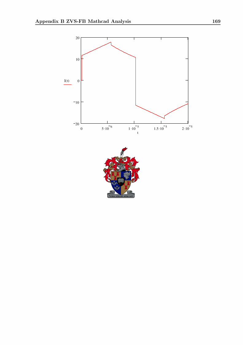
Appendix B ZVS-FB Mathcad Analysis 169
0 5 .10 6 1 .10 5 1.5 .10 5 2 .10 520
10
0
10
20
I t( )
t

Appendix B ZVS-FB Mathcad Analysis 170
Switching Loss Information
MosFet Switching Losses
Assume the circuit switches are numbered as:
| |1 2| |-----@@@---------| |3 4| |
The switch transitions will take place as
1 on end state 101 off start state 5
2 on end state 32 off end state 7
3 on end state 53 off start state 10
4 on end state 84 off end state 2
Switches 2 & 4 will experience the same stressesand switching losses
Likewise switches 1 & 3
MosFet 1 / 3 on
Working with end of State 5
Choosing the time delay length of the state equal to a quarter of the resonant period reveals;
if Wbus Wstored> I13_on 0A:=
if Wbus Wstored< V13_on 0V:=
therefore
W13_on 0J:=

Appendix B ZVS-FB Mathcad Analysis 171
Pfet_s 11.079 W=Pfet_s Pfet_s_on Pfet_s_off+:=
Pfet_s_off 11.079 W=Pfet_s_off W13_off W24_off+( ) fs⋅:=
Pfet_s_on 0 W=Pfet_s_on W13_on W24_on+( ) fs⋅:=
Total Fet Switching Losses
W24_off 138.512 µJ=
W24_off1
2IS2_end⋅ Vbus⋅ tfall⋅:=
With the same assumption as for switches 1 & 3
MosFet 2 / 4 off
W24_on 0J:=
therefore
V24_on 0V:=
Since the transition takes place at the peak of the power delivery cycle the voltagewill allways "ring" to the bus voltage
MosFet 2 / 4 on
W13_off 83.076 µJ=
W13_off1
2IS4_end⋅ Vbus⋅ tfall⋅:=
Neglecting the effect of the output FET capacitance the switching loss can be given by the blocking voltage, the conducting current and the rise time
MosFet 1 / 3 off

Appendix B ZVS-FB Mathcad Analysis 172
Pswitch 11.079 W=Pswitch Pd_s Pfet_s+:=
Pd_s 0 W=Pd_s 2 W24_rr⋅ fs⋅:=
Total Switching Losses
Since the body of the Fet is switched in shunt with the conducting diodethe recovery is soft and slow. To that end the losses in the diode is ignored. The peak currentis also very low, and all current should be conducted through the channel due to lower losses
Diodes 1 & 4
W24_rr 0J:=
thus
However, as the channel of diodes 2 & 4 is switched on while the diode is conducting the resulting diode commutation is regarded as soft and therefore lossless
Irr 28.907 A=
Irr 28.907 A=Irr 2 τdiode⋅ I24_f⋅ di_dt⋅:=
trr 333.155 ns=trr2 τdiode⋅ I24_f⋅
di_dt:=
I24_f 8.36 A=I24_f IS5_end:=
di_dt 86.768 A µs1−
=di_dtVbus
LL:=
Diodes 2 & 4
trrm1
2trr⋅:=
Assuming the softness of the diodes is 1
Diode Reverse Recovery Losses

Appendix B ZVS-FB Mathcad Analysis 173
∆T 6.058 K=∆TPtot
4RθJC RθCS+ RθSS+( )⋅:=
Temperature rise
Ptot
Pout0.508 %=
Ptot 15.24 W=Ptot Pswitch Pconduct+:=
Total Losses
Pconduct 4.16 W=Pconduct 2 W16 W27+ W49+( ) fs⋅:=
Total Conduction Losses
Losses are negligible small
State 5 / 10
W49 17.049 µJ=W49 I492
2 Rds⋅ rt+( )⋅ tS4_end⋅:=
I49 2.912 A=I49 0.5 IS3_end IS4_end−( )⋅:=
State 4 / 9
Losses are negligible small
State 3 / 8
W27 23.099 µJ=W27 I272
2 Rds⋅ rt+( )⋅ tS2_end⋅:=
I27 3.118 A=I27 0.5 IS2_end IS2_0−( )⋅:=
State 2 / 7
W16 1.454 µJ=W16 I162
2 Rds⋅ rt+( )⋅ tS6_end⋅:=
I16 4.18 A=I16 0.5 IS5_end⋅:=
State 1 / 6
Conduction Loss Information

Appendix CBias Flyback Design Documentation
174

Appendix C Bias Flyback Design Documentation 175
Pout3 3.75 W=Pout3 Vout3 Iout3⋅:=
Iout3 250mA:=
Vout3 15V:=
output 3•
Pout2 2.25 W=Pout2 Vout2 Iout2⋅:=
Iout2 150− mA:=
Vout2 15− V:=
output 2•
Pout1 3 W=Pout1 Vout1 Iout1⋅:=
Iout1 200mA:=
Vout1 15V:=
output 1•
Vin 24.183 V=Vin 0.95 2⋅ Vin_ac⋅:=
Vin_ac 18V:=
Input values
a) The supply will provide two isolated control circuits with bias voltage.
b) The output voltages to each of the control circuits is +15V and -15V with a common return
c) The design goal is a 20mV p-p ripple on each of the supplies, with a load regulation of 2%
d) The supply is operated in the discontinous mode to ensure better EMI and load regulation
Notes
Control circuitry bias supply design
Combined 3kW and 65kW plasma torch driving circuit
10W isolated multi output flyback converter

Appendix C Bias Flyback Design Documentation 176
∆Vin 1.821 V=∆VinIin ∆t⋅
Cin:=
Cin 3300µF:=
Cin 2.485 103× µF=Cin Iin
∆t
∆Vin⋅:=
∆t1
2 fmains⋅:=
∆Vin 2.418 V=∆Vin 10% Vin⋅:=
Iin 0.601 A=IinPout
ηdesign Vin⋅:=
Input stage design
Dmax 40%:=
Ts 6.667µs=Ts1
fs:=
fs 150kHz:=
fmains 50Hz:=
ηdesign 80%:=
Pout 11.625 W=Pout Pout1 Pout2+ Pout3+ Pout4+:=
Pout4 2.625 W=Pout4 Vout4 Iout4⋅:=
Iout4 175− mA:=
Vout4 15− V:=
output 4•

Appendix C Bias Flyback Design Documentation 177
Toff 1 Dmax− Ddead−( ) Ts⋅:=
Wcycle_max 96.875 µJ=Wcycle_maxPin
fs:=
Ddead 10%:=
Define a 10% deadtime at the maximum duty cycle to ensure discontinuous operation
a 1:=
a 0.971=aDmax
1 Dmax−( )Vin_min Vds−( )Vout1 Vdiode+( )⋅:=
aN2
N1=
Vdiode 0.3V:=
Vds 0.086V=N 1:=Vds Isw_peak Rds⋅:=
Rds 33 103− Ω⋅:=
Isw_peak 2.599A=Isw_peak4Pin
Vin_min:=
assume a 50% duty cycle
PinPout
ηdesign:=
tmax Dmax fs⋅:=
Vin_min Vin ∆Vin−:=
Turns ratio

Appendix C Bias Flyback Design Documentation 178
Idiode 1.25 A=Idiode 2Iout3
Dmax:=
Vsw_max 70.529 V=Vsw_max 1 Vsw_overshoot+( ) Vin1
NVout1⋅+
⋅:=
Vsw_overshoot 80%:=
Vdiode_r 39.183 V=Vdiode_r Vout1 N Vin⋅+:=
Component Stress
Isw_max 3.249 A=Isw_maxVin_min Dmax⋅
Lp fs⋅:=
Dmin 9.786%=Dmin2 Lp⋅ 7⋅ % Wtrafo⋅ fs
2⋅
Vin2
:=
Dmax 40 %=Dmax2Lp Wtrafo⋅ fs
2⋅
Vin_min2
:=
thus W(in) = W(out)
Lp 18.354 µH=LpVin_min
2Dmax
2⋅
2 Wtrafo⋅ fs2⋅
:=
Wtrafo Wcycle_max:=andIpVin_min
LpDmax⋅ T⋅=but Wtrafo
1
2Lp⋅ Ip
2⋅=
Simplify the multi output circuit to a single output with all the power dissipatedin this output the simplification is valid as the balance is cancelled by working with the equivalent transformer turns ratio

Appendix C Bias Flyback Design Documentation 179
LN
2
Rel=
AL 800.101 nH=ALµ0 µr⋅ Ae⋅
le:=
fill_width 7.1mm:=MLT 24mm:=
kfill 70%:=Awindow 13mm2:=
Constant to offset the effect of magnetic fringingkfringe 1.37:=
lgap 0.32mm:=µr 1525:=
Bmax 280mT:=µ0 4 π⋅ 107−⋅
H
m⋅:=
Ae 12.4mm2:=le 29.7mm:=
Data for E 13/7/4 3C90
Wtrafo 96.875 µJ=
energy storage required
Isw_max 3.249 A=
Lp 18.354 µH=
Transformer design
PRsense_max 0.26 W=PRsense_maxIsw_max
2Rsense⋅
Dmax2
Ts3⋅ 0
Dmax Ts⋅
tt2
d⋅:=
Rsense 0.185Ω=RsenseVsense_max
Isw_max:=
Vsense_max 0.6V:=
Current Measure

Appendix C Bias Flyback Design Documentation 180
Rcu 0.071Ω=Rcuρcu lcu⋅
Acu:=
lcu 0.408 m=lcu MLT N⋅:=
layers_possible 5.086=layers_possibleAwindow
Dcu fill_width⋅:=
layer 17.75=layerfill_width 0.9⋅
Dcu:=
Acu 0.102mm2=Acu
π Dcu2⋅
4:=
Dcu 0.36mm:=
δskin 0.173mm=δskinρcu
π fs⋅ µ0⋅:=
ρcu 17.8 109−⋅ Ω m⋅:=
Wire Data
L 17.811 µH=L AL_gap N2⋅:=
N 17:=
Nd 17.257=NdLp
AL_gap:=
B 0.279T=BAL_gap
Ae
Lp
AL_gap⋅ Isw_max⋅:=
AL_gap 61.629 nH=AL_gap1
Relcore Relgap+:=
Rel Relcore Relgap+:=Relgaplgap
µ0 Ae⋅ kfringe⋅:=
Relcorele lgap−
µ0 µr⋅ Ae⋅:=

Appendix C Bias Flyback Design Documentation 181
Pcu 0.195 W=Pcu Pcu_p Pcu_s+:=
fill 51.12 %=fillAfill 100⋅ %
Awindow:=
Afill 6.646 mm2=Afill Apri Asec+:=
Asec fill_width 2⋅ 1.3⋅ Dcu_s⋅:=
layer_s 35.5=layer_sfill_width 0.9⋅
Dcu_s:=
Pcu_s 0.044 W=Pcu_s Pcu_s1 Pcu_s2+ Pcu_s3+ Pcu_s4+:=
Pcu_s4 8.74 103−× W=Pcu_s4 Iout4
2Rcu_s⋅:=
Pcu_s3 0.018 W=Pcu_s3 Iout32
Rcu_s⋅:=
Pcu_s2 6.421 103−× W=Pcu_s2 Iout2
2Rcu_s⋅:=
Pcu_s1 0.011 W=Pcu_s1 Iout12
Rcu_s⋅:=
Rcu_s 0.285Ω=Rcu_s ρculcu
Acu_s⋅:=
Acu_s 0.025mm2=Acu_s
π Dcu_s2⋅
4:=
Dcu_s 0.18mm:=
Pcu_p 0.151 W=Pcu_p1
2Isw_max
2⋅ Rcu⋅ Dmax⋅:=
Note : The winding structure will fit into two layers therefore the proximity effect in the winding structures can be neglected
Apri 3.323 mm2=Apri fill_width 1.3⋅ Dcu⋅:=

Appendix DPFC Boost Rectifier Design Documents
182

Appendix D PFC Boost Rectifier Design Documents 183
Dave 0.222=DaveVout 2 Vin⋅−
Vout:=
Dpeak 0.293=DpeakVout 2 Vin_min⋅−
Vout:=
Iin_max_nominal 20.736 A=Iin_max_nominal 2 Iin_rms⋅:=
Iin_rms 14.663 A=Iin_rmsPout
Vin pfmin⋅:=
Iin_rms_max 16.129 A=Iin_rms_maxPout
Vin_min pfmin⋅:=
Iin_max 22.81 A=Iin_max2 Pout⋅
Vin_min pfmin⋅:=
Inductor Design
ωin 2 π⋅ fin⋅:=pfmin 0.93:=∆Iin 20%:=
Pout 3kW:=fs 50kHz:=fin 50Hz:=
Vin 220V:=
Vout 400V:=Vin_max 230V:=Vin_min 200V:=
Design of 3kW Boost With pfc

Appendix D PFC Boost Rectifier Design Documents 184
∆Vc% 13.005 %=∆Vc%2∆Vc
Vout:=
∆Vc 26.009 V=∆Vc1
C0
π
ωin
tIL_max_nominal sin ωin t⋅( )⋅ Idc−
d⋅:=
Idc 13.201 A=Idcωin
π0
π
ωin
tIin_max_nominal sin ωin t⋅( )⋅
d⋅:=
Iline_capacitor Iin_max_nominal sin ωin t⋅( )⋅ Idc−=
C 470µF:=
Output Capacitor design, assuming no input current harmonic distortion
IL_max_nominal 22.656 A=IL_max_nominal 2 Iin_rms⋅ 1 0.5 ∆Iin_nominal⋅+( )⋅:=
IL_max 25.091 A=IL_max Iin_max 1 0.5 ∆Iin⋅+( )⋅:=
The Current ripple will always be lower than this as the current magnitude is restrictedBy the control system to follow the input sinusoid
∆Iin_nominal 18.52 %=∆Iin_nominal2 Vin⋅ Dave⋅
fs Iin_max_nominal⋅ L⋅:=
At normal line conditions the ripple at the peak voltage will be
L 360µH:=
Ldesign 363.188 µH=Ldesign2 Vin_min⋅ Dpeak⋅
fs ∆Iin⋅ Iin_max⋅:=
Use the inductor current ripple at the peak of low line input conditions to size the inductor

Appendix D PFC Boost Rectifier Design Documents 185
∆Vcap_rms 12.038 V=
∆Vcap_rms16Im
2
2C2
1
20
n
1
4 n2⋅ 1−( ) 2⋅ n⋅ ω⋅ π⋅
2
=
⋅:=
∆Vcap t( ) 4Im1
20
n
1−( )n cos 2 n⋅ ω⋅ t⋅( )
π 4 n2⋅ 1−( )⋅ C⋅ 2⋅ ω⋅ n⋅
⋅=
⋅:=
∆Vcap t( ) Icharge t( ) Zc⋅=
Icap_rms_100Hz 3.536A=Icap_rms_100Hz4Im
2 3⋅ π⋅:=
Icap_rms 3.626 A=Icap_rms1
20
n
4 Im⋅
2 π⋅ 4 n2⋅ 1−( )⋅
2
=
:=
Icharge t( ) 4 Im⋅
1
20
n
1−( )n cos 2 n⋅ ω⋅ t⋅( )
π 4 n2⋅ 1−( )⋅
⋅=
⋅:= Im 11.781 A=
Assuming I_out remains constant and neglecting high frequency ripple current the capacitor charge current is given by
Iin t( ) Im2
π4
1
20
n
1−( )n cos 2 n⋅ ω⋅ t⋅( )
π 4 n2⋅ 1−( )⋅
⋅=
⋅−
⋅:=
Vout2
Pout53.333 Ω=
Imπ2
Iout_dc:=
ω 314.159 rad s1−⋅=ω 2 π⋅ fin⋅:=
Iout_dc 7.5 A=Iout_dcPout
Vout:=

Appendix D PFC Boost Rectifier Design Documents 186
ω100 2 100⋅ π⋅ rad s1−⋅:=Hbutter s( )
1
s2
2 s⋅+ 1+:=
and second order Butterworth filter transfer function
Hsalen_key s( )
1
R2 C1⋅ C2⋅
s2 2 s⋅
R C1⋅+
1
R2
C1⋅ C2⋅+
=
1F C2
1F C1
R1
R1
+
Butterworth filter
Multiplier setup, feedforward voltage. Average of input voltage.
Input Current Multiplier Setup
∆t 5.013 103−× s=∆t C
∆Vcap
Iout⋅:=
Iout
C
∆Vcap
∆t= Iout 7.5 A=Iout
Pout
Vout:=
∆Vcap 400V 320V−:=CtVcap
dd
Iout=
Minimum time after input loss before V_out = 320V
∆Vcap_fs 0.031 V=∆Vcap_fsIin_max ∆Iin⋅
2 π⋅ fs⋅ C⋅:=
∆Vcap_200Hz 0.665 V=∆Vcap_200Hz1
30
Im
4ω C⋅⋅:=
∆Vcap_100Hz 13.298 V=∆Vcap_100Hz1
3
Im
2ω C⋅⋅:=
Voltage ripple at important harmonics, peak values

Appendix D PFC Boost Rectifier Design Documents 187
1
r2 c1⋅ c2⋅
s2 2 s⋅
r c1⋅+
1
r2
c1⋅ c2⋅+
float 6,15718.5
s2.
177.305 s⋅+ 15718.5+( )1.→
c2 235 109−⋅:=
c1 470 109−⋅:=
r 24 103⋅:=Hsalen_key s( )
1
R2 C1⋅ C2⋅
s2 2 s⋅
R C1⋅+
1
R2
C1⋅ C2⋅+
:=
C2 0.235 µF=C1 0.47 µF=R 23.945 kΩ=
C2C2
km:=C1
C1
km:=R R km⋅:=
kmC1
0.47µF:=
To make C_1 470nF
C2 5.627 103−× F=C1 0.011 F=
C2C2
kω:=C1
C1
kω:=
C2 1F
2
C1:=C1
2F
2:=R 1Ω:=
ωbutter_c 125.664 Hz=kωωbutter_c
1rad s1−⋅
:=
ωbutter_c 2 π⋅ fbutter_c:=fbutter_c 20Hz:=

Appendix D PFC Boost Rectifier Design Documents 188
FeedForw_dcV_in_max 3.106 V=
FeedForw_dcV_in_max2FeedForwdivider_gain 2⋅ Vin_max⋅
π:=
RFF_2 3.3 103× Ω=
RFF_2 FeedForwdivider_gain RFF_1⋅:=RFF_1 220kΩ:=
FeedForwdivider_gain 0.015:=
Vin t( )2 2⋅ Vin_max
π1 2
1
20
n
1−( )n cos 2 n⋅ ω⋅ t⋅( )
1 4 n2⋅−
⋅=
⋅+
⋅:=
Input Voltage can be represented as
trise 0.014 s=trise1.8
ωn:=
ωn 125.664 rad s1−⋅=ωn
1
R2
C1⋅ C2⋅:=
Hgen s( )ωn
2
s2
2ζ ωn⋅ s⋅+ ωn2
+=
Phase100Hz 163.584−=
Phase100Hz arg Hsalen_key i ω100⋅( )( ) 180
π⋅:=
dBdown_100Hz 27.966−=
dBdown_100Hz 20 log Hsalen_key i ω100⋅( )( )⋅:=
Hsalen_key 650irad s1−⋅( ) 0.036− 0.01i−=

Appendix D PFC Boost Rectifier Design Documents 189
RIsense 30Ω:=NCT_ratio1
200:=
Iin_rms_max 16.129 A=
Current Transformers: Nuvotem AS-102 1:200, with 100mH sec mag inductance, 4.5 Ohm sec resistance 75mA output max and recommended term resistance 200Ohm. 20-200kHz
Current Sensing
Css 0.98 µF=CssIss_charge tss⋅
Vss_normal:=
Vss_normal 3V:=tss 0.21s:=Iss_charge 14µA:=
Soft Start and Chip Enable
PhaseFF_200Hz 8.13=PhaseFF_200Hz 180 arg Hsalen_key 2i ω100⋅( )( ) 180
π⋅+:=
VFF_200Hz 4.141 103−× V=VFF_200Hz VFF_200Hz Hsalen_key i 2⋅ ω100( )⋅:=
VFF_200Hz FeedForw_dcV_in_max2
15⋅:=
200 Hz component
PhaseFF_100Hz 163.584−=PhaseFF_100Hz arg Hsalen_key i ω100⋅( )( ) 180
π⋅:=
VFF_100Hz 0.083V=VFF_100Hz VFF_100Hz Hsalen_key i ω100⋅( )⋅:=
VFF_100Hz FeedForw_dcV_in_max2
3⋅:=
100 Hz component
Maximum Feed Forward harmonic values at multiplier input
FeedForw_dcV_in_min 2.701V=
FeedForw_dcV_in_min2FeedForwdivider_gain 2⋅ Vin_min⋅
π:=

Appendix D PFC Boost Rectifier Design Documents 190
Imeasure_max IL_max NCT_ratio⋅:= Imeasure_max 0.125 A=
VIsense_max Imeasure_max RIsense⋅:= VIsense_max 3.764 V=
Check Volt, time product over both CT's
τ 0 0.01, π..:=
Vin τ( ) Vin_min sin τ( )⋅:= IL τ( ) IL_max sin τ( )⋅:=
D τ( )Vout Vin τ( )−
Vout:=
Vsswitch τ( )D τ( ) IL τ( )⋅ RIsense⋅ NCT_ratio⋅
fs:=
Vsdiode τ( )1 D τ( )−( ) IL τ( )⋅ RIsense⋅ NCT_ratio⋅
fs:=
0 0.5 1 1.5 2 2.5 30
1 .10 5
2 .10 5
3 .10 5
4 .10 5Max Volt-s on 2 CT's against input sinus
Vsswitch τ( )
Vsdiode τ( )
τ

Appendix D PFC Boost Rectifier Design Documents 191
Rpk2 18.079 kΩ=Rpk27.5V Ipeak_sense+( ) Rpk1⋅
Ipeak_senseRpk1−:=
Rpk1 10kΩ:=
Ipeak_sense 4.148 V=Ipeak_sense Ipeak NCT_ratio⋅ RIsense⋅:=
Ipeak 27.656 A=Ipeak 1.1 Ilim⋅:=
Peak Current Limit
Rmo 26.022 kΩ=RmoNCT_ratio Ilim⋅ RIsense⋅
Imo_max:=
Ilim 25.142 A=Ilim2 Plim⋅
Vin_min 0.9⋅:=
Plim 3.2kW:=
Imo_max 144.928 µA=Imo_maxVin_min 2⋅ 6 4.5−( )⋅
1 Rac⋅ 2.25⋅:=
Α 7.5 103−×=Α
2.25 V⋅Vin_min
:=
Iac_low 217.391 µA=Iac_low2 Vin_min⋅
Rac:=
Rac 1.301 106× Ω=Rac
2 Vin_max⋅
Iac_max:=
Iac_max 250µA:=
Multiplier setup for Power Limiting

Appendix D PFC Boost Rectifier Design Documents 192
Rvolt2 5.625 kΩ=Rvolt2 Gainvolt_div Rvolt1⋅:=Rvolt1 750kΩ:=
Gainvolt_div 7.5 103−×=Gainvolt_div
Vvolt_set
Vout:=Vvolt_set 3V:=
Vvea_max 5.5V:=
Voltage loop setup
CCA_2 105.844 pF=
CCA_2CCA_1
2 π⋅ fCA_hf_pole⋅ RCA_fb⋅ CCA_1⋅ 1−:=fCA_hf_pole 0.9fs:=
CCA_1 492.689 pF=CCA_11
2 π⋅ fCA_zero⋅ RCA_fb⋅:=fCA_zero
fs
2 π⋅:=
RCA_fb 40.594 kΩ=RCA_fb Max_CA_gain Rmo⋅:=
Max_CA_gain 1.56=Max_CA_gainVramp_dt
dVsense_dt_max:=
dVsense_dt_max 0.167 V µs1−
⋅=dVsense_dt_max dIsense_dt_max− RIsense⋅:=
dIsense_dt_max 5.556− 103−× A µs
1−=dIsense_dt_max dIL_dt_max NCT_ratio⋅:=
dIL_dt_max 1.111− A µs1−
=dIL_dt_maxVout−
L:=
Worst case measured current upslope must be < ramp voltage upslope
Vramp_dt 0.26 V µs1−
⋅=Vramp_dt Vramp_pp fs⋅:=Vramp_pp 5.2V:=
Current Amplifier Compensation

Appendix D PFC Boost Rectifier Design Documents 193
RVA 1.828 kΩ=RVA1
CVA 2⋅ π⋅ 100⋅ Hz:=
CVA 870.742 nF=CVA1
ZC_100Hz 2⋅ π⋅ 100⋅ Hz:=
ZC_100Hz 1.828 kΩ=ZC_100Hz Rin Gainerr_amp⋅:=
Rin 5.583 kΩ=RinRvolt1 Rvolt2⋅
Rvolt1 Rvolt2+:=
Gainerr_amp 0.327=Gainerr_ampGainVA_100Hz
Gainvolt_div:=
GainVA_100Hz_dB 52.198− dB=GainVA_100Hz_dB 20 log GainVA_100Hz( )⋅:=
GainVA_100Hz 2.455 103−×=GainVA_100Hz
∆VVerr
∆Vva_in:=
∆VVerr 0.083V=∆VVerr ∆VVerr_100Hz Vvea_max⋅:=
∆Vva_in 33.6V:=
∆VVerr_100Hz 1.5%:=

AppendixE
Magn
eticD
esignSpread
sheets
Chosen Core
Input Data Material 3C90Core E65/32/27
L 3.60E-04 H V 79000 mm^3I max 23 A le 147 mm I rms 16 A Ae 540 mm^2f 5.00E+04 Hz Window 400 mm^2l airgap 4 mm MLT 150 mmn 46 m 205 gFill Factor 0.7 mu 1830Wire dia 0.8 mm Al 8400 nHStrands 9 3.5367765 A/mm^2 Bsat 420 mT
P core loss 400 kW.m^-3 read from data
penetration depth 0.30 mm Tc 200 deg C
Core reluctance 115154.61Airgap reluctance 5613930.97Total reluctance 5729085.58Wire resistance 0.03 Ohm Wire length 6.9 mCopper loss 6.73 WattCore loss 31.60 WattArea Filled 264.96 mm^2
Bmax 341.98 mTL 0.000369343 H
Saturation FALSEInductance Target 102.60%Wire fit 94.63%Total loss 38.33153259 Watt
PFC Inductor design
194

Appendix
EM
agnetic
Desig
nSpreadsh
eets
195
Chosen Core
Input Data Material 3C90Core ETD 49
L 1.00E-03 H V 24000 mm^3I max 5.5 A le 114 mm I rms 5 A Ae 211 mm^2f 50000 Hz Window 273 mm^2l airgap 1.8 mm MLT 85 mmn 82 m 62 gFill Factor 0.7 mu 1830Wire dia 0.45 mm Al 8400 nHStrands 9 3.4931126 A/mm^2 Bsat 420 mT
P core loss 4 kW.m^-3 read from data
penetration depth 0.30 mm Tc 200 deg C
Core reluctance 231232.81Airgap reluctance 6465332.83Total reluctance 6696565.63Wire resistance 0.08 Ohm Wire length 6.97 mCopper loss 2.10 WattCore loss 0.10 WattArea Filled 149.45 mm^2
mu 64.203751 0.3154463 OhmBmax 319.18 mT Kappa 0.0336586 697.42455 AmpL 0.001004097 HdB 29.01678366 mT
64.20375109Saturation FALSEInductance Target 100.41%Wire fit 78.20%Total loss 2.194710957 Watt
CDR Inductor design

Appendix E Magnetic Design Spreadsheets 196
Ve 79000 mm^-1 Mu 0 1.26E-06 H/mle 147 mm Mu R 1700Ae 540 mm^2 Delta B max 540 mTMLT 150 mm Reluctance 127428Window Area 394 mm^2Window length 39.20 mm
Vbus 400 V Penetration 0.296 mmI pri rms 10 A Wire diameter 0.6 mm I sec rms 10 A length 3 mf 50000 Hz No Litz 8lambda_max 5600 Vmu s R 0.023 OhmN min 20 turns P cu Pri 2.29 WattLmag 3.14 mH Litz dia 2.3 mm
Desired Lleak 50.00 uH Pri inside area 690 mm^2Leak 1.41E-05 Total Pri area 1081.92 mm^2
Winding Area 391.92 mm^2Total sec Area 2332 mm^2Sec inside Area 1906.96 mm^2Winding Area 425.04 mm^2Gap Area 825.04 mm^2
Transformer Design
Leakage Inductance
Core Geometry Magnetic Properties
Design Values Resistance
Area Calculations

Appendix FSelected MATLAB simulation M-files
F.1 CDR and CTR Ripple Current Copper Loss
% Calculates the fourier series of the CDR and CTR currents
% and relevant winding losses.
close all
clear all
k=1:1:40;
rc=0.5e-3;
rd=0.45e-3;
lc = 6.16;
ld = 6.97;
ac = 0.05:0.01:0.99;
ad = ac/2;
Ic=2;
Id=1;
fc=100e3;
fd=50e3;
mu = 4*pi*10^-7;
rho = 17.24*10^-9;
dc = sqrt(rho./(pi*mu*k*fc));
dd = sqrt(rho./(pi*mu*k*fd));
197

Appendix F Selected MATLAB simulation M-files 198
cc = 2*rc*dc*pi - pi*dc.^2;
cd = 2*rd*dd*pi - pi*dd.^2;
for q=1:length(ac)
akc(q,:) = -Ic*(cos(ac(q)*pi*k).^2-1)./(ac(q)*pi^2*k.^2*(ac(q)-1));
bkc(q,:) = Ic*(-sin(ac(q)*pi*k).*cos(ac(q)*pi*k))./(ac(q)*pi^2*k.^2*(ac(q)-1));
akd(q,:) = -Id*(cos(ac(q)*pi*k).^2-1)./(ac(q)*pi^2*k.^2*(ac(q)-1));
bkd(q,:) = Id*(-sin(ac(q)*pi*k).*cos(ac(q)*pi*k))./(ac(q)*pi^2*k.^2*(ac(q)-1));
Pc1(q,:) = (akc(q,:).^2 + bkc(q,:).^2)*lc*rho./(cc*9);
Pd1(q,:) = (akd(q,:).^2 + bkd(q,:).^2)*ld*rho./(cd*9);
Pc1s(q) = sum(Pc1(q,:));
Pd1s(q) = sum(Pd1(q,:));
end
figure
plot(ac,Pc1s)
hold on
plot(ac,Pd1s,’r’)
xlabel(’Effective Duty-cycle’)
ylabel(’I^2R losses (W)’)
legend(’Center Tap’,’Current Doubler’)
figure
plot(ac,Pc1s./(2*Pd1s))
xlabel(’Effective Duty-Cycle’)
ylabel(’Relative Losses’)
t = 0:1e-8:40e-6;
V = 0*t;
V1 = 0*t;
V2 = 0*t;
q = 30;
for m =1:400
ak = -Ic*(cos(ac(q)*pi*m)^2-1)/(ac(q)*pi^2*m^2*(ac(q)-1));
bk = Ic*(-sin(ac(q)*pi*m)*cos(ac(q)*pi*m))/(ac(q)*pi^2*m^2*(ac(q)-1));
V1 = V1 + ak*cos(2*pi*m*fc*t)+bk*sin(2*pi*m*fc*t);
end
figure
plot(t,V1)

Appendix F Selected MATLAB simulation M-files 199
F.2 Transformer Short Circuit Test
% File to process and plot the Short Circuit Test information
% This file creates 3 plots: fft of primary current, fft of
% primary voltage and calcuated leakage inductance. The file
% also outputs the calculated leakage inductance and measurement
% uncertainty to the workspace
%
% F0005CH1.csv Represents the voltage at one of the primary terminals
% F0005CH2.csv Represents the voltage at the other primary terminal
% F0005CH4.csv represents the primary current at 20mV/A
%
% All traces share the the same time base, are measured with the TDS2024
% and are 2500 samples long
close all
Ch1 = csvread(’F0005CH1.CSV’,1,3);
Ch2 = csvread(’F0005CH2.CSV’,1,3);
Ip = csvread(’F0005CH4.CSV’,1,3);
t = Ch1(:,1);
Ch1 = Ch1(:,2);
Ch2 = Ch2(:,2);
Ip = Ip(:,2)/20e-3;
[B,A] = butter(2,0.5);
Ch1f = filtfilt(B,A,Ch1);
Ch2f = filtfilt(B,A,Ch2);
Ipf = filtfilt(B,A,Ip);
P = Ch1-Ch2;
Pf = Ch1f-Ch2f;
Ts = (t(length(t))-t(1))/length(t);
Fs = 1/Ts;
F = linspace(0,Fs,length(t))/1e3;
fftIp = fft(Ipf);
fftIp = fftIp(1:floor(length(Ip)/2));
F = F(1:floor(length(F)/2));
fftIpmax = max(abs(fftIp));
semilogy(F,abs(fftIp)./fftIpmax)

Appendix F Selected MATLAB simulation M-files 200
hold on
h1 = find(fftIp == max(fftIp));
h3 = find(fftIp == max(fftIp((3*h1-10):(3*h1+10))));
h5 = find(fftIp == max(fftIp((5*h1-10):(5*h1+10))));
h7 = find(fftIp == max(fftIp((7*h1-10):(7*h1+10))));
h9 = find(fftIp == max(fftIp((9*h1-30):(9*h1+10))));
fftP = fft(Pf);
fftPmax = max(abs(fftP));
fftIpW = [fftIp(h1) fftIp(h3) fftIp(h5) fftIp(h7) fftIp(h9) ];
FW = [F(h1) F(h3) F(h5) F(h7) F(h9) ];
semilogy(FW,abs(fftIpW)./fftIpmax,’rx’)
axis([0 1200 10^-4 10^0.5])
xlabel(’Frequency (kHz)’)
ylabel(’Normalised Current (dB)’)
fftP = fftP(1:floor(length(P)/2));
fftPW = [fftP(h1) fftP(h3) fftP(h5) fftP(h7) fftP(h9) ];
figure
semilogy(F,abs(fftP)./fftPmax)
hold on
semilogy(FW,abs(fftPW)./fftPmax,’rx’)
axis([0 1200 10^-4 10^0.5])
xlabel(’Frequency (kHz)’)
ylabel(’Normalised Voltage (dB)’)
ZW = fftPW./fftIpW;
LW = abs(ZW)./(2*pi*FW*1e3);
L = mean(LW)
Lsd = std(LW)
figure
plot([1 3 5 7 9],LW/1e-6,’ro’)
hold on
plot(0:10,L*ones(11)./1e-6,’:’)
axis([0 10 0 6])
ylabel(’Measured Inductance (uH)’)

Appendix F Selected MATLAB simulation M-files 201
xlabel(’Harmonic Number’)

Appendix F Selected MATLAB simulation M-files 202
F.3 Output Diode Ringing Waveforms and Snubber Design
% File to process and plot the ZVS overview information
close all
Ch1 = csvread(’F0003CH1.CSV’,1,3);
Ch2 = csvread(’F0003CH2.CSV’,1,3);
Ch3 = csvread(’F0003CH3.CSV’,1,3);
Ch4 = csvread(’F0003CH4.CSV’,1,3);
Ip = csvread(’TEK0000.CSV’,1,3);
t = Ch1((1:2100),1);
t = t-t(1);
Ch1 = Ch1((1:2100),2);
Ch2 = Ch2((1:2100),2);
Ch3 = Ch3((1:2100),2);
Ch4 = Ch4((1:2100),2);
Ip = Ip((1:2100),2)/20e-3;
avep = sum(Ch1(1:150))/500;
aves = sum(Ch3(1:150))/500;
a= aves/avep
Ch3=Ch3/a;
Ch4=Ch4/a;
P = Ch1-Ch2;
S = Ch3-Ch4;
[b,a] = butter(3,0.25);
Ch1f = filtfilt(b,a,Ch1);
Ch2f = filtfilt(b,a,Ch2);
Ch3f = filtfilt(b,a,Ch3);
Ch4f = filtfilt(b,a,Ch4);
Ipf = filtfilt(b,a,Ip);
Pf = Ch1f-Ch2f;
Sf = Ch3f-Ch4f;
subplot(2,2,1)
plot(t./1e-6,Ipf)
hold on
x1 = sum(Ip(840:850))/11;

Appendix F Selected MATLAB simulation M-files 203
x2 = sum(Ip(1060:1070))/11;
dx = x2 - x1;
dt = t(1065) - t(845);
m = dx/dt;
Iapprox = m*t;
k = sum(Ip(850:1060) - Iapprox(850:1060))/length(Ip(850:1060));
Iapprox = Iapprox + k;
plot(t(400:1200)./1e-6,Iapprox(400:1200),’r’)
xlabel(’Time (us)’)
ylabel(’Current (A)’)
title(’Primary Transformer Current’)
axis([0 21 -4 4])
subplot(2,2,2)
plot(t./1e-6,Ch3)
hold on
plot(t./1e-6,Ch4,’r’)
xlabel(’Time (us)’)
ylabel(’Voltage (V)’)
axis([0 21 -10 200])
title(’Transformer Secondary Voltages’)
Idf = Ipf - Iapprox;
b = min( find(Idf<0));
Idf = Idf(min( find(Idf<0)):1000);
tdf = t(b:1000)-t(b);
subplot(2,2,3)
plot(tdf./1e-6,Idf)
xlabel(’Time (us)’)
ylabel(’Current (A)’)
title(’Transient Current’)
axis([0 5.5 -2.5 2.5])
Vdf = Ch4f(b:1000);
tdf = t(b:1000)-t(b);
subplot(2,2,4)
Vdf = Vdf - mean(Vdf);
plot(tdf./1e-6,Vdf)
hold on
xlabel(’Time (us)’)
ylabel(’Voltage (V)’)

Appendix F Selected MATLAB simulation M-files 204
title(’Transient Diode Voltage’)
axis([0 5.5 -100 100])
D = P-S;
%figure(2)
%plot(t,D)
tm1 = find(Vdf==max(Vdf));
tm2 = find(Vdf==max(Vdf(60:80)));
tm3 = find(Vdf==max(Vdf(110:130)));
tm4 = find(Vdf==max(Vdf(160:170)));
tm = [tdf(tm1) tdf(tm2) tdf(tm3) tdf(tm4)];
vm = [Vdf(tm1) Vdf(tm2) Vdf(tm3) Vdf(tm4)];
alpha = -1*log(vm/abs(Vdf(1)))./tm;
alpha = max(alpha);
plot(tdf./1e-6,1.1*Vdf(1)*exp(-alpha*tdf),’r:’)
plot(tdf./1e-6,-1.1*Vdf(1)*exp(-alpha*tdf),’r:’)
I0 = max(Idf)/exp(-alpha*t(find(Idf==max(Idf))));
subplot(2,2,3)
hold on
plot(tdf./1e-6,1.1*I0*exp(-alpha*tdf),’r:’)
plot(tdf./1e-6,-1.1*I0*exp(-alpha*tdf),’r:’)
w = 2*pi*2e6;
L = 4.61e-6 * 4;
C = 1/(L*w^2)
R = alpha*2*L;
Cv = linspace(100e-12,500e-12,100);
Rv = linspace(10,50*R,100);
%Cv = linspace(C2,2*C2,2);
%Rv = linspace(R2,2*R2,2);
zeta = zeros(length(Cv),length(Rv));
for n=1:length(Cv)
for k=1:length(Rv)
on = [L*C*Cv(n)*Rv(k) (L*(C+Cv(n)) + Cv(n)*C*R*Rv(k)) (R*(C+Cv(n)) + Rv(k)*Cv(n)) 1];
r = roots(on);
zeta(n,k) = sin(angle(r(2))-pi/2);

Appendix F Selected MATLAB simulation M-files 205
end
end
figure
mesh(Rv,Cv./1e-12,zeta)
view(-11.5,22)
xlabel(’Resistance (Ohm)’)
ylabel(’Capacitance (pF)’)
zlabel(’Damping Ratio’)
Cv = 470e-12;
for k=1:length(Rv)
on = [L*C*Cv*Rv(k) (L*(C+Cv) + Cv*C*R*Rv(k)) (R*(C+Cv) + Rv(k)*Cv) 1];
r = roots(on);
zeta2(k) = sin(angle(r(2))-pi/2);
end
figure
plot(Rv,zeta2)
xlabel(’Damping Resistance (Ohm)’)
ylabel(’Damping Ratio’)
figure
Rv = Rv(find(zeta2 == max(zeta2)));
on1 = [L*C R*C 1];
bo1 = [1];
on2 = [L*C*Cv*Rv (L*(C+Cv) + Cv*C*R*Rv) (R*(C+Cv) + Rv*Cv) 1];
bo2 = [Rv*Cv 1];
step(bo2,on2,3e-6)
hold on
step(bo1,on1,’r’)
title(’’)
legend(’Without Snubber’,’With Snubber’)

Appendix GSchematics, Manufacturing Drawings and
Documentation
The following modifications has been introduced to the attached circuit diagrams.
1. Apply the piggyback breadboard modifications sub-circuits as described in the cir-
cuit diagram
2. The voltage loop error amplifier of the phase shift controller is left uncompensated.
Apply the input current command directly to U17 pin 2.
3. The source connection of the top switches is wrong. Connect the sources to pin 6
of U18 and 19, respectively.
4. Short circuit the C68-70 & R65-67 junction track to FB ground (U17 pin 12 & 20)
5. During this design IRF460A MosFets was used in lieu of the indicated CoolMos
switches. However it is recommended that IGBT’s fitting the footprint be found.
6. The Gate and Source pins of Q 3-6 is reversed. This was solved by bending the gate
pin upwards and bending the source pin sideways for connection to the substrate.
7. L10 is shorted out.
8. Connect a decoupling resistance between U12 pin 8 and U13 pin 11. Alternatively as
described in the design document disconnect U12 pin 8 and use the voltage divider
thevenin resistance as decoupling.
9. Connect an 100 kΩ between pins 18 and 11 of U17. Lift pint 18. This is done in
conjunction with the piggyback current sensing modification.
206
Copyright © 2022 FDOKUMEN