A SOFT SWITCHING DC–DC CONVERTER WITH HIGH VOLTAGE GAIN AND LOW OVER VOLTAGE STRESS AND HARMONICS
8
A SOFT SWITCHING DC–DC CONVERTER WITH HIGH VOLTAGE GAIN AND LOW OVER VOLTAGE STRESS AND HARMONICS By ABSTRACT In this paper a soft switching dc–dc converter with high voltage gain and low over voltage stress and harmonics is proposed. It consists of a ZVS boost converter stage and a ZVS half-bridge converter stage and the two stages are merged into a single stage. The ZVS boost converter stage pro- vides a continuous input current and ZVS operation of the power switches. The ZVS half-bridge converter stage provides a high voltage gain. The principle of operation and the system analysis are presented in this paper. Theoretical analysis and performance of the proposed converter were verified on a 100W experimental prototype operating at 108 kHz switching frequency. Here both the ZVS and ZCS is done. It reduces the overvoltage stress and harmonics. Keywords: Boost Converter, Coupled Inductor, High Voltage Gain, Reverse Recovery, Zero-voltage Switching (ZVS). SINU K J * K SATHISHKUMAR ** * SCAD Institute of Technology, Coimbatore. ** RVS Faculty of Engineering, Coimbatore. *** **** Assistant Professor, Assistant Professor, Professor & Head, SCAD Institute of Technology. Assistant Professor, Department of Electrical & Electronics Engineering ,SCAD Institute of Technology, Palladam INTRODUCTION In dc–dc converters with high voltage gain, there are several requirements such as high voltage gain [1], [2], [3], [5], [6], low reverse-recovery loss [7], [8], soft-switching characteristic [16], low-voltage stress across the switches, electrical isolation, continuous input current, and high efficiency. In order to meet these requirements, various topologies are introduced. In order to extend the voltage gain, the boost converters with coupled inductors are proposed in [9] and [10]. The voltage gain is extended but the continuous input current characteristic is lost, and the efficiency is degraded due to hard switching of power switches. In [11], a step-up converter based on a charge pump and coupled inductor is suggested. Its voltage gain is around 10 but its efficiency is not high enough due to the switching loss. In [12], a high-step-up converter with coupled inductors is suggested to provide high voltage gain and a continuous input current. How- ever, its operating frequency is limited due to the hard switching of the switches. The converters suggested in [13] have a similar drawback. Their switching frequencies are limited due to the hard-switching operation. In order to increase the efficiency and power density, soft-switching technique is required in dc– dc converters. In this paper, various soft-switching techniques are suggested. Generally, there is a trade off between soft-switching characteristic and the high voltage gain. It is because of an inductor which is related to soft-switching limits of the voltage gain. In order to solve these problems, a zero-voltage-switching (ZVS) dc–dc converter with high voltage gain is proposed. In Figure 1, it consists of a ZVS boost converter stage to make the input current continuous and provide ZVS functions and a ZVS half-bridge converter stage to provide the high voltage gain. Since a single power processing stage can be a more efficient and cost-effective solution, both stages are merged and share power switches to increase the system efficiency and simplify the structure. Since in both the stages have the ZVS function, ZVS operation of the power switches can be obtained with wider load variation. Moreover, due to the ZVS function of the boost converter stage, the design of the half-bridge converter stage can be focused on the high voltage gain, Thus the, high voltage gain is easily obtained. ZVS RESEARCH PAPERS l i-manager’s Journal o Electrical Vol. 7 No. 4 l n Engineering, April - June 2014 1 K. RAJANGAM MUTHUKUMARASAMY *** ****
Transcript of A SOFT SWITCHING DC–DC CONVERTER WITH HIGH VOLTAGE GAIN AND LOW OVER VOLTAGE STRESS AND HARMONICS
A SOFT SWITCHING DC–DC CONVERTER WITH HIGH VOLTAGE GAIN AND LOW OVER VOLTAGE STRESS AND HARMONICS
By
ABSTRACT
In this paper a soft switching dc–dc converter with high voltage gain and low over voltage stress and harmonics is
proposed. It consists of a ZVS boost converter stage and a ZVS half-bridge converter stage and the two stages are
merged into a single stage. The ZVS boost converter stage pro- vides a continuous input current and ZVS operation of the
power switches. The ZVS half-bridge converter stage provides a high voltage gain. The principle of operation and the
system analysis are presented in this paper. Theoretical analysis and performance of the proposed converter were
verified on a 100W experimental prototype operating at 108 kHz switching frequency. Here both the ZVS and ZCS is done.
It reduces the overvoltage stress and harmonics.
Keywords: Boost Converter, Coupled Inductor, High Voltage Gain, Reverse Recovery, Zero-voltage Switching (ZVS).
SINU K J * K SATHISHKUMAR **
* SCAD Institute of Technology, Coimbatore.** RVS Faculty of Engineering, Coimbatore.
*** ****
Assistant Professor, Assistant Professor,
Professor & Head, SCAD Institute of Technology.Assistant Professor, Department of Electrical & Electronics Engineering ,SCAD Institute of Technology, Palladam
INTRODUCTION
In dc–dc converters with high voltage gain, there are
several requirements such as high voltage gain [1], [2], [3],
[5], [6], low reverse-recovery loss [7], [8], soft-switching
characteristic [16], low-voltage stress across the switches,
electrical isolation, continuous input current, and high
efficiency. In order to meet these requirements, various
topologies are introduced. In order to extend the voltage
gain, the boost converters with coupled inductors are
proposed in [9] and [10]. The voltage gain is extended but
the continuous input current characteristic is lost, and the
efficiency is degraded due to hard switching of power
switches. In [11], a step-up converter based on a charge
pump and coupled inductor is suggested. Its voltage gain
is around 10 but its efficiency is not high enough due to the
switching loss. In [12], a high-step-up converter with
coupled inductors is suggested to provide high voltage
gain and a continuous input current. How- ever, its
operating frequency is limited due to the hard switching of
the switches. The converters suggested in [13] have a
similar drawback. Their switching frequencies are limited
due to the hard-switching operation. In order to increase
the efficiency and power density, soft-switching
technique is required in dc– dc converters. In this paper,
various soft-switching techniques are suggested.
Generally, there is a trade off between soft-switching
characteristic and the high voltage gain. It is because of
an inductor which is related to soft-switching limits of the
voltage gain.
In order to solve these problems, a zero-voltage-switching
(ZVS) dc–dc converter with high voltage gain is proposed.
In Figure 1, it consists of a ZVS boost converter stage to
make the input current continuous and provide ZVS
functions and a ZVS half-bridge converter stage to provide
the high voltage gain. Since a single power processing
stage can be a more efficient and cost-effective solution,
both stages are merged and share power switches to
increase the system efficiency and simplify the structure.
Since in both the stages have the ZVS function, ZVS
operation of the power switches can be obtained with
wider load variation. Moreover, due to the ZVS function of
the boost converter stage, the design of the half-bridge
converter stage can be focused on the high voltage gain,
Thus the, high voltage gain is easily obtained. ZVS
RESEARCH PAPERS
li-manager’s Journal o Electrical Vol. 7 No. 4 l n Engineering, April - June 2014 1
K. RAJANGAM MUTHUKUMARASAMY *** ****

operation of the power switches reduce the switching loss
during the switching transition and improves the overall
efficiency. The theoretical analysis is verified by a 100W
experimental prototype with 24–393 V conversion.
1. Analysis of the Proposed Converter
The equivalent circuit of the proposed converter is shown
in Figure 2. The ZVS boost converter stage consists of a
coupled inductor L , the lower switch Q , the upper switch c 1
Q , the auxiliary diode D , and the dc-link capacitor C . 2 a dc
The diodes D and D represent the intrinsic body diodes Q 1 Q 2
of Q and Q The capacitors C and C are the parasitic 1 2. Q1 Q2
output capacitances of Q and Q . The coupled inductor 1 2
L is modeled as the magnetizing inductance L ,the c m1
leakage inductance L , and the ideal transformer that k1
has a turn ratio of 1:n (n = N /N ). The ZVS half-bridge 1 1 s 1 p 1
converter stage consists of a transformer T, the switches Q 1
and Q , the output diodes D and D , the dc-blocking 2 o1 o2
capacitors C and C , and the output capacitor C . The B 1 B 2 o
transformer T is modeled as the magnetizing inductance
L , the leakage inductance L and the ideal transformer m 2 k 2
that has a turn ratio of 1:n (n2 = NS2/Np2. The theoretical
waveforms of the proposed converter are shown in Figure
3. The switches Q and Q are operated asymmetrically 1 2
and the duty ratio D is based on the switch Q . The 1
operation of the proposed converter in one switching
period T can be divided into seven which is shown in s
Figure 4. Just before the Mode 1, the upper switch Q , the 2
auxiliary diode D , and the output diode D are a o1
conducting. The magnetizing current i of L arrives at its m1 c
minimum value I and the auxiliary diode current i m2 Da
arrives at its maximum value I . The current i has its Da L
maximum value I dc converter.L1
Mode 1 [t , t ]: At t0 , the upper switch Q is turned OFF. 0 1 2
Then, the capacitor C starts to be charged and the Q2
voltage v across Q increases toward V dc. Q2 2
Simultaneously, the capacitor C is discharged and the Q1
voltage v across Q decreases toward zero. With an Q1 1
assumption that the output capacitances C and C of Q1 Q2
the switches are very small and all the inductor currents
are not changed, the transition time interval Tt 1 can be
considered as follows
Tt1 = t1 t0 =(CQ1 + CQ2 )Vd / IL1 + (n1 + 1) IDa Im12
(1)
Mode 2 [t1, t2 ]: At t1, the voltage vQ1 across the lower
switch Q1 becomes zero and the body diode DQ1 is
turned ON, then, the gate signal for Q1 is applied. Since
the current has already flown through the body diode DQ1
and the voltage vQ1 is maintained as zero before the
switch Q1 is turned ON, the zero-voltage turn-ON of Q1 is
achieved. Since the voltage vp1 across the magnetizing
inductance Lm1 is Vin, the magnetizing current im1
increases linearly from its minimum value Im2 as follows:
im1 (t) = Im12 + Vin/Lm1 (t − t1 ) . (2)
Since the voltage vLk1 across the leakage inductance Lk1
is– (n1Vin+Vdc), the auxiliary diode current iDa linearly
decreases from its maximum value IDa as follows
iDa(t) = IDa − n1Vin + Vdc/Lk1(t − t1 ). (3)
From (2) and (3), the input current iin is determined as
follows
iin (t) = im1 (t)−ip1 (t) = im1 (t)−n1 iDa(t) = Im12 −n1Ida +
Figure 1. Proposed soft-switching dc–dc converter with high voltage gain
Figure 2. Equivalent circuit of the proposed soft-switching dc–dc converter.
RESEARCH PAPERS
li-manager’s Journal o Electrical Vol. 7 No. 4 l n Engineering, April - June 2014 2

Vin/ Lm1(t − t1) + n1 · n1Vin + Vdc/Lk1(t − t1 )
(4)
Since vp2 is –(Vdc–VCB1) and vLk2 is VCB2+n2Vin , the
magnetizing current im2 and the diode current iDo1 are
given by
im2 (t) = Im21 − Vdc − VCB1Lm2(t − t1 ) (5)
iDo1 (t) = −iCB2(t) = IDo1 − VCB2 + n2Vin/Lk2(t − t1 ) .
(6)
In this mode, the primary current ip2 , the coupled
inductor current iL , and the switch current iQ1 can be
obtained from the following relations
Figure 3. Theoretical waveforms. Figure 4. Operating modes.
RESEARCH PAPERS
li-manager’s Journal o Electrical Vol. 7 No. 4 l n Engineering, April - June 2014 3
ip2 (t) = n2 iCB2(t) (7)
iL (t) = im2 (t) ip2 (t) (8)
iQ1 (t) = iin (t) iDa(t) iL (t). (9)
Mode 3 [t2, t3 ]: At t2 , the current iCB2 changes its
direction. The output diode current iD 1 decreases to zero o
and the diode Do1 is turned OFF. Then the output diode
Do2 is turned ON, and its current will increases linearly.
Since the current changing grate of D 1 is controlled by o
the leakage inductance Lk2 of the transformer T, its
reverse-recovery problem is alleviated. Since vp2 is same
as in Mode 2 and vLk2 is n2Vin+VCB2–Vo, the current im2
and the diode current iDo2 are given by
im2 (t) = im2 (t2 ) – Vin/ Lm2(t t2 ) (10)
iDo2 (t) = iCB2(t) = VCB2 + n2Vin – Vo/Lk2(t t2 ) . (11)
The currents ip2, iL, and iQ1 can be obtained from the
same relations in Mode 2. In this mode, the voltages vp1
and vLk are equal to those in Mode 2. Therefore, the
magnetizing current im1, the auxiliary current iDa, and the
input current i in change with the same slopes as in Mode
2.
Mode 4 [t3, t4 ]: At t3, the auxiliary diode current iDa
decreases to zero and the diode Da is turned OFF. Since
the changing rate of the diode current iDa is controlled by
the leakage inductance Lk1 of the coupled inductor Lc
and its reverse recovery problem is alleviated. Since the
voltage vp1 across the magnetizing inductance Lm1 is
the input voltage Vin, the magnetizing current im1
increases linearly with the same slope as in Modes 2 and 3
as follows
im1 (t) = im1 (t3) + Vin/Lm1(t t3 )
Since the auxiliary diode current iDa is zero, the input
current iin is equal to the magnetizing current im1. At the
end of this mode, the magnetizing current im1 arrives at its
maximum value Im11. Since the voltages vp2 and vLk2
are not changed in this mode, the slopes of the current
im2 , iCB2, and iL are not changed.
Mode 5 [t4, t5 ]: At t4, the lower switch Q1 is turned (12) OFF,
then the capacitor CQ1 starts to be charged and the
voltage vQ1 across Q1 increases toward Vdc.
Simultaneously the capacitor CQ2 is discharged and the
voltage vQ2 across Q2 decreases toward zero. With the
same assumption as in Mode1, the transition time interval
Tt2 can be determined as follows
Tt2 = t5 t4 =(CQ1 + CQ2 )Vdc/IL2 + Im11 . (13)
Mode 6 [t5, t6 ]: At t5 , the voltage vQ2 across the upper
switchQ2 becomes zero and the body diode DQ2 is
turned ON. Then, the gate signal is applied to the switch
Q2 . Since the current has already flown through the body
diode DQ2 and the voltage vQ2 is maintained as zero
before the turn-ON of the switch Q2 ,the zero-voltage turn-
ON of Q2 is achieved. Since the voltage vp1 across the
magnetizing inductance Lm1 is –(Vdc–in), the
magnetizing current im1 decreases linearly from its
maximum value Im11 as follows
im1 (t) = Im11 Vdc – Vin/Lm1(t t5 ) . (14)
Since the voltage vLk1 across the leakage inductance Lk
is n1 (Vdc–Vin ), the auxiliary diode current iDa linearly
increases from zero as follows:
iDa(t) = n1 (Vdc Vin )/Lk1(t t5 ). (15)
From (14) and (15), the input current iin is determined as iin
(t) = Im11 Vdc –Vin/Lm1(t t5 ) n21(Vdc Vin )/Lk1(t t5 ).
(16)
Since the voltage vp2 is vCB1 (= DVin/(1–D)) and vLk2 is
–(Vo–VCB2 +n2DVin/(1–D)), the magnetizing current im2
and the diode current iDo2 are given by
im2 (t) = Im22 + DVin/Lm2 (1 D)(t t5 ) (17)
iDo2 (t) = iCB2(t) = IDo2 Vo VCB2 + (n2DVin/(1D))/L(tt5)
(18)
Mode 7 [t6, t7 ]: At t6 , the current iCB2 changes its
direction. The output diode current iDo2 decreases to zero
and the diode Do2 is turned OFF. Then the output diode
Do1 is turned ON and its current increases linearly. Similar
to Do1 , the current changing rate of Do2 is controlled by
the leakage inductance Lk2 of the transformer T and its
reverse-recovery problem is alleviated. Since vp2 is the
same as in Mode 6 and vLk 2 is VCB2– n2DVin/(1–D), the
current im2 and the diode current iDo2 are given by
im2 (t) = im2 (t6) + D Vin/Lm2 (1 D)(t t6 ) (19)
iDo1 (t) = iCB2(t) = VCB2 (n2DVin/(1 D))/Lk2(t t6 ) (20)
and the voltage nQ1 across Q1 increases toward Vdc.
RESEARCH PAPERS
li-manager’s Journal o Electrical Vol. 7 No. 4 l n Engineering, April - June 2014 4
Simultaneously
The currents ip2 and iL can be obtained from the same
relations in Mode 2. In this mode, the voltages vp1 and
vLk1 are equal to those in Mode 6. Therefore, the
magnetizing current im1, the auxiliary current iDa, and the
input current iin change with the same slopes as in Mode
2.
2. Characteristic and Design Parameters
2.1 Voltage Gain of the Boost Converter Stage
Referring to this voltage waveform vp1 in Figure 3, the
voltsecond balance law gives
VinDTs − (Vdc − Vin) (1 − D) Ts = 0. (21)
From (21), the voltage gain of the proposed ZVS boost
converter stage is obtained by
Vdc/Vin=1/1 – D (22)
which is the same as that of the conventional CCM boost
converter.
2.2 Auxiliary Diode Current Reset Timing Ratio d1
By applying the volt-second balance law to the voltage
waveform vLk1, the auxiliary diode current reset timing
ratio d1 is determined by
d1 = n1D(1 D)/n1(1 D) + 1. (23)
2.3 Maximum Auxiliary Diode Current Ida
From Modes 6 and 7, the maximum auxiliary diode
current IDa is obtained by
IDa = n1DVinTs/Lk1 (24)
2.4 DC-Blocking Capacitor Voltage VCB1
Referring to the voltage waveform vp2 in Figure 3, the
voltsecond balance law gives
VCB1 (1 − D) Ts − (Vdc − VCB1)DTs = 0. (25)
From (22) and (25), the dc-blocking capacitor voltage
VCB1 is obtained by
VCB1 = DVin/1 – D (26)
2.5 Maximum Output Diode Currents IDo1 and Ido2
From Modes 2 and 7, the maximum output diode current
IDo1 can be written as follows
IDo1 = n2Vin + VCB2/Lk2d2Ts =VCB2 + (n2DVin/(1 D))/Lk2
((1 D) d3 ) Ts (27)
From Modes 3, 4, and 6, the maximum output diode
current IDo2 can be written as follows:
IDo2 = n2Vin + VCB2 – Vo/Lk2(D d2 )
Ts = Vo VCB2 + (n2DVin/(1 D))/Lk2d3Ts . (28)
2.7 Output Voltage Vo2 of the Half-Bridge Converter
Stage
From (27) and (28), the dc-blocking capacitor voltage
VCB2 and the output voltage Vo can be derived as follows
VCB2 = Dd2 (D/(1D))d3/1D + d2d3 n2Vin ( 29)
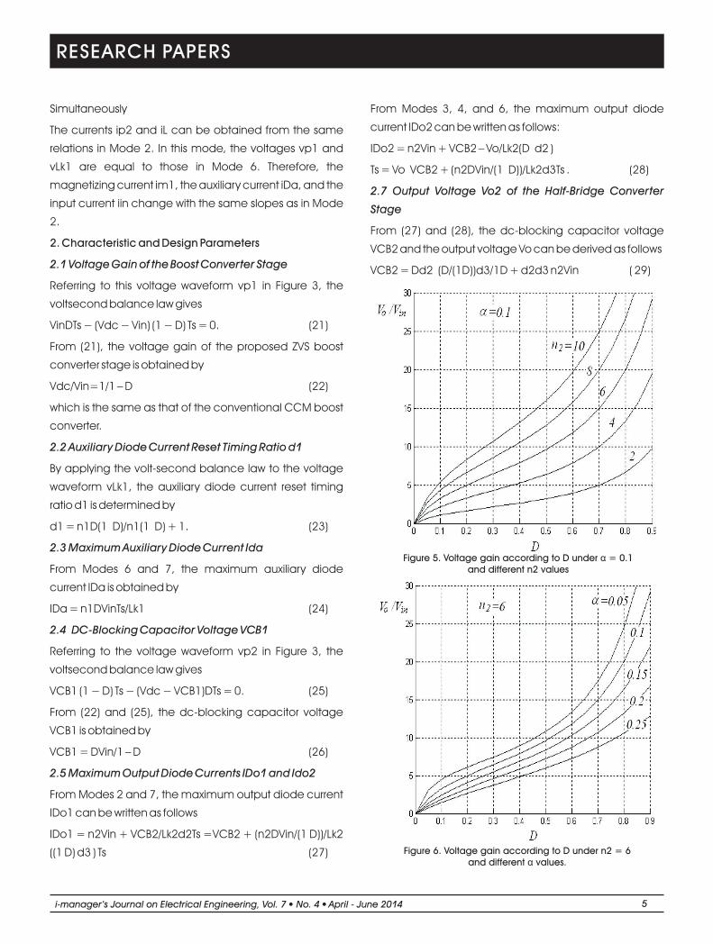
Figure 5. Voltage gain according to D under α = 0.1 and different n2 values
Figure 6. Voltage gain according to D under n2 = 6 and different α values.
RESEARCH PAPERS
li-manager’s Journal o Electrical Vol. 7 No. 4 l n Engineering, April - June 2014 5

Vo = D d2(D/(1 D))d3/ (D d2 + d3) (1D+ d2 d3 n2Vin ( 30)
2.8 Output Diode Current Reset Timing Ratios d2 and d3
Since the average value of the current iCB2 should be
zero, the following relation can be obtained
(1 D + d2 d3 ) IDo1 = (D d2 + d3 ) Ido2 (31)
From (27) to (31), the relation between d2 and d3 is
obtained by
d2/d3= D/1 – D (32)
Since the average value of the current im2 is zero, its peak
values
Im21 and Im22 have the same value as follows
Im21 = Im22 = DVinTs/2Lm2 . (33) From Figure 2, the
output current Io can be represented by
Io = (1D+ d2 d3 ) IDo1/2= (D d2 + d3 ) IDo2/2 (34)
From (27), (28), (32), and (34), d2 and d3 are obtained by
d2 = αD (35)
2.8 Voltage Gain M of the Proposed DC–DC Converter
From (22), (30), (35), and (36), the voltage gain M of the
proposed converter is given by
M = Vo/Vin=
n2D(1 2α)/(D(1 2α) + α) (1 α (1 2α)D) . (38)
Figures 5 and 6 show the voltage gain M according to the
dutycycle D. In Figure 5, the voltage gain M under α = 0.1
and several n2 values is shown. As n2 increases, the
voltage gain M increases. In Figure 6, the voltage gain M
under n2 = 6 and several α values is shown. As α increases,
the voltage gain M decreases. Namely, larger Lk2
reduces the voltage gain M. Since α depends on Io , Vin ,
and D, Figures 5 and 6 can be used in obtaining n2 and α
only at the maximum duty cycle under the full load
condition.
2.9 Input Current Ripple
The input current ripple ∆iin can be written by
∆iin = Im11 Im12 + n1IDa = n12Lm1 + Lk1Lm1Lk1/ DVinTs
(39)
To reduce the input current ripple below a specific value
I=, the magnetizing inductance Lm1 should satisfy the
following condition
2.10 ZVS Conditions
As is seen in Figure 3, both the boost converter stage and
the half-bridge converter stage have ZVS function. From
Figure 3, the ZVS condition for Q2 is given by
Im11 + IL2 = Im11 + Im22 + n2IDo2 > 0.
Since the current values Im11, Im22, and IDo2 have
positive values, the ZVS condition for Q2 is always satisfied.
Similarly, for ZVS of Q1 , the following condition should be
satisfied
Im21 + n2IDo1 + (n1 + 1) IDa Im12 > 0.
(41)
(42)
Figure 7 Maximum leakage inductance Lk 1,max for ZVS.
(40)
Figure 8. Output waveform
RESEARCH PAPERS
li-manager’s Journal o Electrical Vol. 7 No. 4 l n Engineering, April - June 2014 6
>

The terms Im21 and n2IDo1 are from the half-bridge
converter stage and the terms (n1 + 1)IDa and Im12 are
from the boost converter stage. If the boost converter
stage is designed to satisfy the above inequality (42)
regardless of the status of the half bridge converter stage,
ZVS of the proposed converter is always accomplished. In
this case, the leakage inductance Lk1 of the coupled
inductor Lc should satisfy the following condition
Lk1 <(n1 + 1) n1DVinTs/Po/Vin (43)
Since the current values Im11, Im22, and IDo2 have
positive values, the ZVS condition for Q2 is always satisfied.
Similarly, for ZVS of Q1 , the following conditions should be
satisfied
Im21 + n2IDo1 + (n1 + 1) IDa Im12 > 0. (42)
The terms Im21 and n2IDo1 are from the half-bridge
converter stage and the terms (n1 + 1)IDa and Im12 are
from the boost converter stage. If the boost converter
stage is designed to satisfy the above inequality (42)
regardless of the status of the half bridge converter stage,
ZVS of the proposed converter is always accomplished. In
this case, the leakage inductance Lk1 of the coupled
inductor Lc should satisfy the following condition
Lk1 < (n1 + 1) n1DVinTsPo/Vin (43)
where Po is the output power and the minimum value
Im12 of the magnetizing current im1 is approximated as
Po/Vin.
3. Experimental Results
To verify the theoretical analysis of the proposed dc–dc
converter, a 100W prototype is implemented. The input
voltage Vin and the output voltage Vo are 24 V and 393 V,
respectively. The switching frequency fs is 108 kHz.
According to the design parameters given in Section 2
and the circuit parameters can be selected. The turn ratio
n1 of the coupled inductor Lc is calculated from (23). By
choosing a proper d1, the turn ratio n1 can be
determined. Here, d1 is chosen as 0.88 and n1 is selected
as n = 0.5. In Figures 5 and 6, α and n2 are selected as 0.1
and 6, respectively. From (43), the leakage inductance
Lk1 of the coupled inductor Lc can be determined. Figure
7 shows the maximum leakage inductance Lk1,max
according to normalized output current. In order to obtain
ZVS regardless of the load condition, Lk1 needs to be
designed to satisfy the ZVS condition at full load. From
Figure 7, Lk1 is selected as 16.75 µH. Then the magnetizing
inductance Lm1 is designed as 800 µH form40) with I= =
2.7 A. According to α, the leakage inductanceLk2 of the
transformer T is selected as 170 µH. The magnetizing
inductance Lm2 of the transformer T is selected as 474 µH.
The dc-blocking capacitors CB1 and CB2 are 6.6 µF and
2.2µF, respectively. The aluminum electrolytic capacitors
470 µF/ 100 V and 47 µF/450 V are used as the dc-link
capacitor Cdc and the output capacitor Co ,
respectively. Figure 8. shows the Output waveform &
Figure 9 shows the Measured efficiency.
Conclusion
A soft switching dc–dc converter with high voltage gain
and low overvoltage stress and harmonics was
suggested. It can achieve ZVS turn-ON of two power
switches while maintaining CCM. In addition, the reverse-
recovery characteristics of the output diodes were
significantly improved by controlling the current changing
rate with the use of the leakage inductance of the
transformer. The proposed converter presents a higher
efficiency and a wider ZVS region and it reduces the over
voltage stress and harmonics
References
[1]. F. Blaabjerg, Z. Chen, and S. B. Kjaer, (2004). “Power
electronics as efficient interface in dispersed power
generation systems,” IEEE Trans. Power Electron., Vol. 19, Figure 9. Measured efficiency.
RESEARCH PAPERS
li-manager’s Journal o Electrical Vol. 7 No. 4 l n Engineering, April - June 2014 7

No. 5, pp. 1184–1194, Sep.
[2]. R. J. Wai, W. H. Wang, and C. Y. Lin, (2008). “High-
performance stand-alone photovoltaic generation
system,” IEEE Trans. Ind. Electron., Vol. 55, No. 1, pp.
240–250, Jan.
[3]. R. J. Wai and W. H. Wang, (2008). “Grid-connected
photovoltaic generation system,” IEEETrans. CircuitsSyst. I,
Reg. Papers, Vol. 55, No. 3, pp. 953–964, Apr.
[4]. R. J. Wai, C. Y. Lin, C. Y. Lin, R. Y. Duan, and Y. R. Chang,
(2008). “Highefficiency power conversion system for
kilowatt-level distributed generation unit with low input
voltage,” IEEE Trans. Ind. Electron., Vol. 55, No. 10, pp.
3702–3714, Oct.
[5]. S. K. Mazumder, R. K. Burra, and K. Acharya, (2007).
“A ripple-mitigating and energy-efficient fuel cell power-
conditioning system,” IEEE Trans. Power Electron., Vol. 22,
No. 4, pp. 1437–1452, Jul.
[6]. K. Kobayashi, H. Matsuo, and Y. Sekine, (2006).
“Novel solar-cell power supply system using a multiple-
input DC–DC converter,” IEEE Trans. Ind. Electron., Vol. 53,
No. 1, pp. 281–286, Feb.
[7]. Q. Zhao, F. Tao, F. C. Lee, P. Xu, and J. Wei, (2008). “A
simple and effective to alleviate the rectifier reverse-
recovery problem in continuous-currentmode boost
converter,” IEEE Power Electron., Vol. 16, No. 5, pp.
649–658, Sep.
[8]. Q. Zhao and F. C. Lee, (2003). “High-efficiency, high
step-up dc–dc converters,” IEEE Power Electron., Vol. 18,
No. 1, pp. 65–73, Jan.
[9]. Q. Zhao, F. Tao, Y. Hu, and F. C. Lee, (2001). “Active-
clamp DC/DC converter using magnetic switches,” in
Proc. IEEE Appl. Power Electron. Conf.,
[10]. D. A. Grant, Y. Darroman, and J. Suter, (2007).
“ Synthesis of tapped-inductor swi tched-mode
converters,” IEEE Trans. Power Electron., Vol. 22, No. 5, pp.
1964–1969, Sep.
[11]. D. A. Grant, Y. Darroman, and J. Suter, (2007).
“ Synthesis of tapped-inductor swi tched-mode
converters,” IEEE Trans. Power Electron., Vol. 22, No. 5, pp.
1964–1969, Sep.
[12]. K. I. Hwu and Y. T. Yau, (2010). “Voltage-boosting
converter on charge pump and coupling inductor with
passive voltage clamping,” IEEE Trans. Ind. Electron., Vol.
57, No. 5, pp. 1719–1727, May.
[13]. S. V. Araujo, R. P. Torrico-Bascope, and G. V. Torrico-
Bascope, “Highly efficient high step-up converter for fuel-
cel l power process ing based on three-state
commutation cell,” IEEE Trans. Ind. Electron., Vol. 57, No.
6,
RESEARCH PAPERS
li-manager’s Journal o Electrical Vol. 7 No. 4 l n Engineering, April - June 2014 8
Sinu is currently working as an Assistant Professor in the Department of Electrical & Electronics Engineering, SCAD Institute of Technology, Palladam. He has completed his BE in Instrumentation & Control Engineering from Anna University on 2009 and ME Power Electronics & Drives from Anna University by 2012. He has the 4 years of teaching experience.
Sathishkumar is currently working as an Assistant Professor ,Dept of Electronics & Communication Engineering RVS Faculty of Engineering, Sulur. He has completed his BE Electronics& Communication Engineering from Bharathiyar University by 2005 and ME in Embedded systems from Anna University by 2013. He has the 7 years of teaching experience.
Dr. K. Rajangam is currently working as a Professor & Head, SCAD Institute of Technology. He has completed his Ph.D., from Anna University by 2014. He has the 15 years of teaching experience.
Muthukumarasamy is currently working as an Assistant Professor, Department of Electrical & Electronics Engineering ,SCAD Institute of Technology, Palladam
ABOUT THE AUTHORS