Sensorless Adaptive Voltage Control for Classical DC ... - MDPI
Upload
khangminh22Category
view
1download
0
João Marcus Soares Callegari
Minimum Dc-Link Voltage Control Strategy forEfficiency and Reliability Improvement in
Two-Stage Photovoltaic Inverters
Belo Horizonte, MG
2021


João Marcus Soares Callegari
Minimum Dc-Link Voltage Control Strategy for Efficiency
and Reliability Improvement in Two-Stage Photovoltaic
Inverters
Dissertacao submetida a banca examinadoradesignada pelo Colegiado do Programa dePos-Graduacao em Engenharia Eletrica doCentro Federal de Educacao Tecnologica deMinas Gerais e da Universidade Federal deSao Joao Del Rei, como parte dos requisitosnecessarios a obtencao do grau de Mestre emEngenharia Eletrica.
Centro Federal de Educacao Tecnologica de Minas Gerais
Programa de Pos-Graduacao em Engenharia Eletrica
Orientador: Prof. Dr. Heverton Augusto Pereira
Coorientador: Prof. Dr. Allan Fagner Cupertino
Belo Horizonte, MG
2021

Callegari, João Marcus SoaresC157m Minimum Dc-Link voltage control strategy for efficiency and
reliability improvement in two-stage photovoltaic inverters / João MarcusSoares Callegari. – 2021.
119 f.: il., gráfs, tabs., fotos.
Dissertação de mestrado apresentada ao Programa de Pós-Graduaçãoem Engenharia Elétrica em associação ampla entre a UFSJ e oCEFET-MG.
Orientador: Heverton Augusto Pereira.Coorientador: Allan Fagner Cupertino.Dissertação (mestrado) – Centro Federal de Educação Tecnológica de
Minas Gerais.
1. Sistemas de energia fotovoltaica – Controle automático – Teses.2. Energia – Fontes alternativas – Teses. 3. Energia – Consumo – Teses.4. Confiabilidade (Engenharia) – Teses. 5. Geração de energiafotovoltaica – Inovações tecnológicas – Teses. I. Pereira, HevertonAugusto. II. Cupertino, Allan Fagner. III. Centro Federal de EducaçãoTecnológica de Minas Gerais. IV. Universidade Federal de São Joãodel-Rei. V. Título.
CDD 621.31244
Elaboração da ficha catalográfica pela bibliotecária Jane Marangon Duarte,CRB 6o 1592 / Cefet/MG

João Marcus Soares Callegari
Minimum Dc-Link Voltage Control Strategy for Efficiencyand Reliability Improvement in Two-Stage Photovoltaic
Inverters
Dissertacao submetida a banca examinadora designada pelo Colegiado do Programa dePos-Graduacao em Engenharia Eletrica do Centro Federal de Educacao Tecnologica deMinas Gerais e da Universidade Federal de Sao Joao Del Rei, como parte dos requisitosnecessarios a obtencao do grau de Mestre em Engenharia Eletrica.
Trabalho aprovado em 16 de Abril de 2021.
Comissao Examinadora:
Prof. Dr. Heverton Augusto PereiraOrientador
Prof. Dr. Allan Fagner CupertinoCoorientador
Prof. Dr. Wesley PeresConvidado 1
Prof. Dr. Demercil de Souza Oliveira JuniorConvidado 2
Belo Horizonte, MG
2021

A minha famılia, mentores e amigos.


Agradecimentos
Nao e nenhum exagero dizer que este trabalho jamais seria possıvel sem a ajuda
de inumeras pessoas, as quais sou e serei eternamente grato. E impossıvel expressar em
poucas palavras a minha gratidao por todos voces, mas tentarei mesmo assim.
Em primeiro lugar, nao posso deixar de agradecer a Deus, por sempre se fazer
presente em minha vida. Obrigado por ter me iluminado durante a confeccao deste trabalho
e ter colocado pessoas maravilhosas a minha volta nesta longa batalha.
Agradeco profundamente aos meus pais, Magda e Marcus, pelo incentivo, amor,
confianca e apoio durante todos os dias da minha vida. Fico imensamente feliz em
saber que voces compartilharam do meu sonho e depositaram confianca em mim, antes
mesmo do inıcio deste trabalho. Voces sempre se mostraram fonte de confianca, dedicacao,
determinacao, carinho, zelo e perseveranca. Sempre estiveram presentes para me mostrar
qual o melhor caminho a ser seguido. Todas as minhas conquistas sao frutos do exemplo
dado por voces. Nos sabemos que nao foi facil sair do interior do Espırito Santo e chegar
ate aqui. Me esforco todos os dias para deixa-los orgulhosos e espero estar correspondendo,
ao menos um pouco, as expectativas.
O meu muito obrigado aos meus irmaos, Luıs Filipe e Pedro Paulo, que sempre se
preocuparam com o meu bem estar. A forca de vontade em vencer de voces sempre foi
uma inspiracao para mim. Obrigado pelos bons momentos, motivacoes, inumeros favores,
brigas e reconciliacoes. Deixo registrado a minha eterna gratidao.
Ao meu avo, meu maior exemplo, por todos os conselhos e conversas. Obrigado pela
amizade, pelas nossas caminhadas, pelos ensinamentos, pela paciencia, pela honestidade e
por ser essa pessoa que irradia vida. O senhor vem acompanhando todos os meus passos
desde sempre e, mesmo que este trabalho esteja em uma lıngua desconhecida para o senhor
e cheio de sımbolos estranhos, tenho certeza que o senhor sera o primeiro a elogia-lo.
Agradeco tambem as minhas avos e tia-avo, Ignes, Deusa e Yole, por terem atuado
ativamente na minha formacao. Apesar de nao estarem mais aqui, tenho certeza que estao
torcendo pelo meu sucesso. Agradeco tambem o apoio que recebi dos meus familiares, em
especial a minha madrinha e tio, Maria Aparecida e Sebastiao, por acreditarem em mim
nos momentos em que nao me julguei capaz.
Agradeco infinitamente a minha namorada, Bia. Eu precisaria de uma vida para
agradece-la. Eu a admiro pela sua sinceridade e companheirismo sem medidas. Sua presenca
nesta caminhada se fez necessaria em cada momento, como fonte de carinho, seguranca e
gratidao. Saiba que minhas vitorias sao gracas a voce, que nunca hesitou em me auxiliar,

esteve presente nos bons e maus momentos e fez os meus dias melhores.
Agradeco ao prof. Heverton pela disponibilidade de me orientar neste projeto de
mestrado. Apesar de desafiadora, essa transicao em degrau de migrar de um ambiente de
simulacao para programacao pratica de DSP me ajudou muito a crescer. Obrigado pela
amizade, apoio, conselhos de vida, diponibilidade, sugestoes e por ajudar a abrir portas
que antes pareciam estar fechadas.
Agradeco ao prof. Allan por atuar diretamente no meu crescimento como pesquisador
em eletronica de potencia, com quem tive imenso prazer de trabalhar de forma direta.
Muito obrigado pelo apoio, disponibilidade, incessantes reunioes, puxoes de orelha (porque,
nao?) e preciosas contribuicoes para este trabalho ser desenvolvido.
Ao Centro Federal de Educacao Tecnologica de Minas Gerais (CEFET-MG) e
a Gerencia de Especialistas em Sistemas Eletricos de Potencia (GESEP-UFV), pela
oportunidade de aprimorar meus conhecimentos, por todo apoio fornecido e suporte
prestado durante o desenvolvimento deste trabalho. Aproveito a oportunidade para
agradecer ao prof. Erick e ao Lucas Xavier, pela constante troca de informacoes, conhecimento,
esforco e por auxiliarem no start-up inicial da bancada de testes utilizada neste trabalho.
Suas preciosas contribuicoes, sugestoes e implementacoes durante os finais de semana serao
sempre lembradas por mim.
A PHB Solar, por fornecer o inversor comercial utilizado durante os desenvolvimentos
deste projeto de mestrado. Por ultimo, mas nao menos importante, agradeco a todos os
meus colegas e amigos do GESEP, cujo apoio e amizade estiveram presentes em todos os
momentos.

“Se cheguei ate aqui foi porque
me apoiei no ombro dos gigantes.”
(Isaac Newton)


Resumo
Hoje em dia, os sistemas fotovoltaicos (FV) conectados a rede tem mostrado um crescimento
notavel na potencia instalada global. A eletronica de potencia, por meio do inversor FV,
desempenha um papel importante no que diz respeito a operacao segura e eficiente dos
sistemas solares, atuando como uma porta de entrada crıtica entre o arranjo FV e a
rede eletrica. Esforcos recentes sao impulsionados por uma demanda de reducoes nos
custos de manutencao e de tecnologia, principalmente por meio do aumento da eficiencia e
confiabilidade do inversor fotovoltaico. Diferentes topologias de circuitos, tecnologias de
integracao, componentes de hardware, estrategias de modulacao e estrategias de controle
estao sendo propostas ultimamente para atingir esses objetivos. Dentre as tecnicas, a
ultima pode ser considerada importante para direcionar o desenvolvimento de novas
estrategias visando aumentar a atratividade dessa fonte de energia renovavel. Por exemplo,
estrategias baseadas na alteracao de firmware podem reduzir os custos de manutencao
sem exigir mudancas de hardware de inversores comercialmente disponıveis, alem da facil
atualizacao dos inversores disponıveis atualmente. Por esse motivo, diversas estrategias
baseadas em firmware sao propostas na literatura para melhorar a confiabilidade e a
eficiencia do conversor. No entanto, poucas delas analisam o inversor programado com
tensao do barramento cc adaptativa mınima. Tendo em vista os pontos acima mencionados,
esta dissertacao de mestrado propoe a operacao com tensao do barramento cc mınima
para melhoria da eficiencia e confiabilidade dos inversores fotovoltaicos de dois estagios
conectados a rede. O objetivo principal e calcular em tempo real a mınima tensao do
barramento cc necessaria para a transferencia de energia entre o arranjo FV e a rede,
buscando reduzir as perdas nos capacitores e dispositivos semicondutores. Alem disso,
expressoes analıticas sao desenvolvidas para avaliar o potencial de reducao dos estresses
de corrente e tensao nos componentes crıticos a confiabilidade do conversor. A viabilidade
dessa estrategia de controle e demonstrada por meio de resultados experimentais em regime
permanente e durante variacoes da amplitude da rede e operacao reativa indutiva/capacitiva
do conversor. A eficiencia e a confiabilidade sao calculadas com base em um estudo de
caso de um inversor fotovoltaico comercial de 3 kW, considerando perfis de campo de
irradiancia solar, temperatura ambiente e amplitude de tensao da rede de uma instalacao
no centro-oeste do Brasil. Os resultados indicam que a solucao proposta leva a uma
resposta dinamica adequada, reducao de perdas de energia, aumento da confiabilidade do
sistema e e cada vez mais interessante com o aumento da frequencia de chaveamento. Como
nenhum hardware adicional e necessario para implementar a proposta, essa abordagem
pode ser usada para melhorar a confiabilidade dos inversores fotovoltaicos atuais atraves
de modificacoes simples no firmware dos sistemas FV ja instalados.
Palavras-chaves: Controle, melhoria da eficiencia, mınima tensao do barramento cc,

confiabilidade, inversor fotovoltaico de dois estagios conectado a rede.

Abstract
Nowadays, grid-connected photovoltaic (PV) systems have shown remarkable growth in
global installed power. Power electronics, through the PV inverter, play an important
role with regard to the safe and efficient operation of solar systems, acting as a critical
gateway between PV array and the utility grid. Recent efforts are driven by a demand for
reduction of technology and maintenance costs, mainly by increasing the inverter efficiency
and reliability. Different circuit topologies, integration technologies, hardware components,
modulation and control strategies are being proposed to achieve these goals. Among the
techniques, the latter can be considered an important direction for the development of
new strategies to increase the attractiveness of this renewable energy source. For instance,
firmware-based strategies can reduce maintenance costs without requiring hardware changes
of commercially available PV inverters and provide a straightforward retrofit of the current
inverter technology. For this reason, several firmware-based strategies are proposed in the
literature to improve converter reliability and efficiency. However, few of them analyze
the inverter programmed with minimum adapted dc-link voltage. In view of the points
aforementioned, this master thesis proposes the minimum dc-link voltage operation for
efficiency and reliability improvement of two-stage grid-connected PV inverters. The
main goal is to compute in real-time the minimum dc-link voltage required for power
transfer, aiming at reducing losses on capacitors and semiconductor devices. Also, analytical
expressions are developed to assess the potential reduction of current and voltage stresses in
the converter reliability-critical components by the first time. The feasibility of this control
strategy is demonstrated by experimental results in steady-state and during grid voltage
amplitude variations and converter reactive inductive/capacitive operation. The efficiency
and system-level reliability are computed based on a case study of a 3-kW commercial PV
inverter, considering real-field mission profiles of solar irradiance, ambient temperature
and grid voltage amplitude of an installation in the center-west of Brazil. The results
indicate that the proposed solution leads to suitable dynamic response, reduced power
losses (specially with the increase in the switching frequency) and increased system-level
reliability. Since no additional hardware is required to implement the proposal, this
approach can be used to improve the reliability of current PV inverter technology through
simple modifications in the firmware of installed systems.
Key-words: Control, efficiency improvement, minimum dc-link voltage, system-level
reliability, two-stage grid-connected PV inverter.


List of Figures
Figure 1 – (a) Summarized timeline of two-level full-bridge transformerless inverter
topology developments. (b) Classical FB topology, (c) H5 topology, (d)
HERIC topology, (e) DCPB topology and (f) ZVR topology. . . . . . . 34
Figure 2 – Structure and main control functions of a typical two-stage single-phase
grid-connected PV system. . . . . . . . . . . . . . . . . . . . . . . . . . 35
Figure 3 – Overview of strategies proposed to improve static converters efficiency
and reliability in the literature. . . . . . . . . . . . . . . . . . . . . . . 37
Figure 4 – Master thesis structure. . . . . . . . . . . . . . . . . . . . . . . . . . . 40
Figure 5 – (a) Schematic of a two-stage single-phase grid-connected PV system.
(b) Boost converter control block diagram. . . . . . . . . . . . . . . . . 44
Figure 6 – (a) Block diagram SOGI-PLL structure. Frequency response of the
closed-loop transfer function of (b) Hα(s) and (c) Hβ(s). . . . . . . . . 45
Figure 7 – (a) Bipolar, (b) unipolar and (c) hybrid modulation structures. . . . . 46
Figure 8 – Typical configurations and control structures of single-phase grid-connected
PV systems. (a) Hardware overview. (b) Inner control loop in αβ-reference
frame. (c) Outer control loop for two-stage PV systems in dq-reference
frame (d) Complete inverter cascade-control structure. . . . . . . . . . 47
Figure 9 – (a) Magnitude and (b) phase response of the PR-controller for different
ki,c. . . . . . . . . . . . . . . . . . . . . . . . . . . . . . . . . . . . . . . 49
Figure 10 – (a) Average model of the single-phase PV system. (b) Simplified average
model of the single-phase PV system, using the Pade approximant
approach. (c) Simplified phasor diagram of the converter, considering
different grid voltage and ϕ scenarios. (d) Range of synthesized voltage
by the converter required to remain grid-connected, as a function of the
injected current, ϕ and grid voltage (Sb = 3300 VA and Vb = 311 V). . 51
Figure 11 – Adaptive dc-link voltage reference according to model (2.7) as a function
of the converter operating angle, considering (a) rated fixed current
injection and (b) grid voltage set at 1 pu (filter impedance equal to
0.01 + j0.1 pu). . . . . . . . . . . . . . . . . . . . . . . . . . . . . . . . 52
Figure 12 – (a) IGBT typical collector current waveforms. Typical current waveforms
considering traditional operation (dc-link voltage set at v∗dcf ) and minimum
dc-link voltage operation, for boost (a) IGBT and (b) diode. . . . . . . 54
Figure 13 – Typical boost capacitor current waveform, composed of the current
drained from the PV array and the boost inductor current. . . . . . . . 55

Figure 14 – RMS-current stress evaluation of the dc-link capacitor bank according
to the modulation index and duty-cycle operating ranges between the
minimum and fixed dc-link voltage (setup parameters are used under
rated power). . . . . . . . . . . . . . . . . . . . . . . . . . . . . . . . . 58
Figure 15 – Flowchart diagram to assess the PV inverter reliability performance. . . 59
Figure 16 – Structure of a cross section of standard power device. . . . . . . . . . . 60
Figure 17 – Flowchart of mission profile-based approach to estimate the efficiency
and lifetime of two-stage single-phase PV inverters. . . . . . . . . . . . 62
Figure 18 – One-year mission profile of: (a) solar irradiance, (b) ambient temperature
and (c) grid voltage. . . . . . . . . . . . . . . . . . . . . . . . . . . . . 63
Figure 19 – Thermal impedance models: (a) Cauer-model. (b) Foster-model. . . . . 64
Figure 20 – Simplified thermal model of (a) power devices and (b) al-caps, from the
electrical domain to thermal domain linked by power losses. . . . . . . 65
Figure 21 – Power devices and al-caps total losses, considering different solar irradiance
ang grid voltage conditions: (a) Inv. IGBTs and (b) inv. diodes. (c)
Dc-link capacitor (partnumber B43630C5397M0 from TDK). (d) boost
IGBT and (e) boost diode. (f) Boost capacitor (partnumber B43630C5397M0
from TDK). . . . . . . . . . . . . . . . . . . . . . . . . . . . . . . . . . 66
Figure 22 – Flowchart for the reliability evaluation of power devices and capacitors. 67
Figure 23 – Pulsed losses in power devices: (a) real loss and approximate loss by
a sum of two-square pulses. (b) Corresponding real and approximate
junction temperature. . . . . . . . . . . . . . . . . . . . . . . . . . . . 68
Figure 24 – Flowchart of Monte-Carlo simulation for power devices and capacitors. 69
Figure 25 – Procedure for assembling the core and windings loss look-up table of
magnetic components. . . . . . . . . . . . . . . . . . . . . . . . . . . . 71
Figure 26 – (a) Experimental setup. (b) PV inverter components: 1) boost capacitor,
2) boost inductor, 3) dc-link capacitor bank, 4) filter inductors, 5) filter
capacitor, 6) conditioning electronic circuits. (c) Schematic of connection
between hardware and DSP. . . . . . . . . . . . . . . . . . . . . . . . . 74
Figure 27 – (a) Experimental results of grid angle amplitude and angular frequency
estimated by SOGI-PLL, normalized from 0 to 3.3V (rated TMS320F28034
DSP voltage output). (b) Experimental waveforms of the injected current
and differential voltage synthesized by the converter, using a unipolar
modulation strategy (vs [250 V/div]; io [2 A/div]; and time [20 ms/div]).
Zoomed view in the high-harmonic frequencies voltage spectrum is also
showed. (c) Experimental steady-state results of the current-controlled
PV inverter (vo [250 V/div]; vdc [250 V/div]; io and ig [10 A/div]; and
time [10 ms/div]). . . . . . . . . . . . . . . . . . . . . . . . . . . . . . . 77

Figure 28 – Cascade-control performance of single-phase PV inverter. Dc-link voltage
controlled at (a) 400 V and (b) 360 V, with PV array operation under
300 W/m2 and 25 C. (c) Dc-link voltage controlled at 360 V and PV
array operation under 500 W/m2. (d) Dc-link voltage control dynamics,
when the voltage reference is changed from 400 to 360 V. (vo [250 V/div];
io [2 A/div]; vdc [100 V/div]; vdc ripple [1 V/div] and time [1000 and
10 ms/div]). Array (e) I-V curve and (f) P-V curve operating points
calculated by the control when disturbances are performed. . . . . . . . 79
Figure 29 – Dc-component effect on single-phase PV systems. . . . . . . . . . . . . 84
Figure 30 – Flowchart of the offset mitigation algorithm caused by the measurement
biases of the ac sensors. . . . . . . . . . . . . . . . . . . . . . . . . . . 85
Figure 31 – (a) Diagram of a typical single-phase PV system. (b) Closed loop of
current control architecture, modeled with delay due to sampling and
PWM scheme. . . . . . . . . . . . . . . . . . . . . . . . . . . . . . . . . 86
Figure 32 – Open-loop Bode diagram of the non-compensated system and compensated
with PR and PIR: (a) Magnitude. (b) Phase. . . . . . . . . . . . . . . . 86
Figure 33 – Closed-loop Bode diagram of the compensated system with PR and
PIR: (a) Magnitude and phase of G1(s). (b) Magnitude and phase of
G2(s). . . . . . . . . . . . . . . . . . . . . . . . . . . . . . . . . . . . . 87
Figure 34 – (a) Cascade-control dynamic performance of single-phase PV inverter
when the proposed dc-component mitigation strategy is enabled. vo
[100 V/div]; io [2 A/div]; vdc ripple [2.5 V/div] and time [10 ms/div]).
Corresponding dynamics result when the PIR controller is enabled: (b)
Current dc-component injection. (c) Line-frequency ripple amplitude of
the dc-link voltage. . . . . . . . . . . . . . . . . . . . . . . . . . . . . . 88
Figure 35 – Simulation results of the grid-connected PV inverter for fixed and
minimum dc-link voltage strategies: PV array operating conditions for
(a) traditional and (b) proposed techniques. (c) Active and reactive
power injected into the grid. (d) Dc-link voltage dynamics for traditional
and proposed approach during power and grid voltage steps. (e) Injected
current dynamic for traditional and proposed approach during power
and grid voltage steps. Zommed view of the current injected during
transient events: (f) Reactive-inductive power injection (lagging power
factor). (g) Reactive-capacitive power injection (leading power factor).
(h) Grid overvoltage step (unitary power factor). . . . . . . . . . . . . . 92
Figure 36 – Synthesized voltage reference and modulator carrier peak-to-peak during
voltage and power steps: (a) Fixed dc-link voltage strategy. (b) Minimum
dc-link voltage strategy. . . . . . . . . . . . . . . . . . . . . . . . . . . 94

Figure 37 – Experimental results of the two-stage grid-connected PV inverter (grid
voltage [250 V/div]; injected current [5 A/div]; dc-link voltage [150
V/div], PV array voltage [150 V/div] and time [100 ms/div]). (a) Fixed
and (b) minimum dc-link voltage operation when a 10% grid overvoltage
variation is applied. Minimum dc-link voltage operation when an (c)
inductive- and (d) capacitive-reactive power step is performed. . . . . . 95
Figure 38 – Simulated temperature dynamics of reliability-critical components after
system disturbance application, at 5 s. Hot-spot temperature of (a)
dc-link and (b) boost capacitors. (c) Inverter IGBT junction temperature
and (d) its transient zoom. (e) Inverter diode junction temperature and
(f) its transient zoom. Junction temperature of (g) boost IGBT and (h)
boost diode. . . . . . . . . . . . . . . . . . . . . . . . . . . . . . . . . . 97
Figure 39 – Junction temperature and hot-spot temperature: (a) inv. IGBT, (b) inv.
diode, (c) dc-link capacitor, (d) boost IGBT, (e) boost diode and (f)
boost capacitor. . . . . . . . . . . . . . . . . . . . . . . . . . . . . . . . 98
Figure 40 – Junction temperature and hot-spot temperature histograms for all 1-year
MP samples translated to thermal loading (5,256,000 samples): (a) inv.
IGBT, (b) inv. diode, (c) dc-link capacitor, (d) boost IGBT, (e) boost
diode and (f) boost capacitor. . . . . . . . . . . . . . . . . . . . . . . . 98
Figure 41 – (a) Active power at the inverter output injected in the grid after
computing the component losses, for the proposed and traditional
strategies. (b) Sum of power loss contributions from semiconductors,
al-caps and magnetic devices, for the proposed and traditional strategies.
(c) Power losses histogram of all inverter components for 1-year MP
samples (5,256,000 samples). . . . . . . . . . . . . . . . . . . . . . . . . 99
Figure 42 – (a) Converter efficiency for fsw = 6 kHz and 20 kHz, considering the
proposed and traditional control strategies. (b) Euro efficiency gain for
the converter switching at 6, 12, 15, 18 and 20 kHz. (c) PV inverter
energy losses with fsw = 20 kHz, separated by components and evaluated
during 1-year mission profile. (d) Total energy losses considering the
switching frequency equal to 6, 12, 15, 18 and 20 kHz. . . . . . . . . . 100
Figure 43 – (a) Component and (b) system-level unreliability functions, considering
both strategies. . . . . . . . . . . . . . . . . . . . . . . . . . . . . . . . 102

List of Tables
Table 1 – Analytical expressions of current and voltage stresses on PV semiconductors. 56
Table 2 – Analytical expressions of current and voltage stresses on PV capacitors. 57
Table 3 – Failure modes, critical failure mechanisms and critical stressors of the
reliability-critical PV components (Wang et al., 2014; Nichicon, 2020). . 61
Table 4 – Foster thermal impedance for IKW40N60H3 power module from Infineon. 64
Table 5 – Lifetime model parameters and their experimental test limits. . . . . . . 68
Table 6 – Parameters of the single-phase grid-connected PV system. . . . . . . . . 76
Table 7 – Controller gains of the single-phase grid-connected PV system. . . . . . 76
Table 8 – Range and precision of 32-bit fixed-point number for different Q format
representation (Texas Instruments, 2010). . . . . . . . . . . . . . . . . . 120


List of abbreviations and acronyms
ac Alternating Current
ADC Analog-to-digital converters
al-caps Aluminum electrolytic capacitors
Al Aluminum
BPF Band-pass filter
CCS Code Composer Studio
CDF Cumulative Density Function
CEFET Centro Federal de Educacao Tecnologica de Minas Gerais
d Direct-axis component
dq Synchronous Reference Frame
DCBP Direct Current by Pass
dc Direct Current
DPWM Discontinuous Pulse-width Modulation
DSP Digital Signal Processor
DCB Direct copper-bonded
EPS Electric Power System
ESR Equivalent series resistance
FB Full Bridge
FFT Fast Fourier Transform
GESEP Gerencia de Especialistas em Sistemas Eletricos de Potencia
GPIO General purpose I/O
IEC International Electrotechnical Commission
IEEE Institute of Electrical and Electronics Engineers

IGBT Insulated Gate Bipolar Transistor
LPF Low-pass filter
MAF Moving Average Filter
MG Minas Gerais
MLC Multi-layer ceramic capacitors
MP Mission Profile
MPP Maximum Power Point
MPPF Metallized polypropylene film capacitors
MPPT Maximum Power Point Tracking
MR Miner’s Rule
NPC Neutral Point Clamped
P&O Perturb and Observe
PCC Point of common coupling
PDF Probability Density Function
PF Power factor
PI Proportional Integral
PIR Proportional integral resonant
PIM Plastic IGBT modules
PLL Phase-Locked Loop
PoF Physics-of-Failure
PR Proportional Resonant
PV Photovoltaic
PWM Pulse-width Modulation
q Quadrature-axis component
RMS Root mean square
Si Silicon

SHE Selective Harmonic Elimination
SOGI Second-order Generalized Integrator
SPWM Sinusoidal Pulse-width Modulation
SRF Synchronous Reference Frame
SVPWM Space Vector PWM
TF Transfer function
THD Total harmonic distortion
TI Texas Instruments
UFV Universidade Federal de Vicosa
VSI Voltage source inverter
WBG Wide-bandgap
ZVR Zero Voltage Rectifier


List of symbols
A Constant scaling factor
AL Effective inductor area
ar Bond-wire aspect ratio
Bx Time when x % of samples have failed
B1 Lifetime model parameter
B0 Lifetime model parameter
BL Operating magnetic flux density
Bmax Maximum magnetic flux density
β Weibull shape parameter
C Lifetime model parameter
Cdc Dc-link capacitor
Cf LCL filter capacitance
Cpv Boost converter capacitor
Cth Thermal capacitance of the power device layers
∆I Boost inductor current ripple
∆vdc dc-link voltage variation
∆T Temperature fluctuation
∆Tj Junction temperature fluctuation
d1−5 Converter diodes
d Boost converter duty cycle
d∗ Boost converter reference duty cycle
Ea Activation energy
EF European efficiency index

EFp European efficiency index F for the proposed strategy
EFt European efficiency index F for the traditional strategy
ESRdc Dc-link capacitor ESR
ESRpv Boost converter capacitor ESR
fc Cross-over frequency
fd Factor for diode reliability evaluation
fs Sampling frequency
fsw Switching frequency
ϕ Displacement angle between converter output current and voltage
f(x) Weibull PDF
F (x) Weibull CDF or component unreliability function
Fi(x) IGBT component unreliability function
Fd(x) Diode component unreliability function
Fc(x) Capacitor component unreliability function
Fsys(x) System unreliability function
G Solar irradiance
GEF European efficiency gain
γ Lifetime model parameter
h Harmonic order
Hα Transfer function of SOGI band-pass filter
Hβ Transfer function of SOGI low-pass filter
Hs Transfer function of the delay that depends on the PWM scheme
i∗α Inner loop reference current
ic Generic capacitor operating current
iCpv Boost capacitor current
iCpv ,rms Boost capacitor RMS current

idc dc-link capacitor current
idc,rms dc-link capacitor RMS current
Idc Injected dc current
i∗d Direct grid current reference
id Direct grid current
id1,avg Diode average current
id1,rms Diode RMS current
id5 Boost converter diode current
id5,avg Boost diode average current
id5,rms Boost diode RMS current
iinv Inverter input current
iinv,avg Inverter input average current
iinv,rms Inverter input RMS current
iL Generic inductor operating current
iLb Boost converter inductor current
io Instantaneous controlled current
Io Controlled current amplitude
ipv PV array current
i∗q Quadrature grid current reference
iq Quadrature grid current
is1,avg IGBT average current
is1,rms IGBT RMS current
is5 Boost converter IGBT current
is5,avg Boost IGBT average current
is5,rms Boost IGBT RMS current
k Modulation strategy factor

kb Boltzmann constant
ki,b Boost converter controller: integral gain
kp,b Boost converter controller: proportional gain
ki,c Inner loop controller: integral gain
kp,c Inner loop controller: proportional gain
ki,dc dc-link voltage outer loop controller: integral gain
kp,dc dc-link voltage outer loop controller: proportional gain
ki,q Reactive power outer loop controller: integral gain
kp,q Reactive power outer loop controller: proportional gain
ki,pll SRF-PLL: integral gain
kp,pll SRF-PLL: proportional gain
L Equivalent filter inductance
Lc Capacitor lifetime under operating condition
LC′
Total 1-year static lifetime consumption
Lb Boost converter inductance
Lf Converter-side LCL filter inductance
Lg Grid-side LCL filter inductance
Lo Capacitor lifetime under testing condition
M Converter modulation index
m Modulation signal
N Number of samples read from the ADC channels in the initialization
process
Nf Number of cycles to failure for each MP stress condition
N′f Equivalent-static number of cycles to failure per year
NL Inductor number of turns
ni Number of IGBTs

nd Number of Diodes
nc Number of Capacitors
η Weibull scale parameter
ηx% Efficiency at z % of inverter rated power
PL,core Inductor core losses
PL,w Inductor winding losses
PL Inductor total losses
Pmpp PV array rated power
Ppv PV array instantaneous power
po(t) Instantaneous active power injected into the grid
po(t) Oscillating active power injected into the grid
po(t) Average active power injected into the grid
Po Active power injected into the grid
Pt Power device total losses
q SOGI selective gain
Q∗ Reactive power reference
Q Reactive power processed
R Equivalent filter resistance
Rb Boost converter internal resistance
Rf Converter-side LCL filter internal resistance
Rg Grid-side LCL filter internal resistance
Rh Heatsink thermal resistance
Rthc Capacitor thermal resistance
Rth Thermal resistance of the power device layers
Rc−h Thermal resistance between the device case and heatsink
Rh−a Thermal resistance between the heatsink and ambient

s1−5 Converter IGBTs
Ta Ambient temperature
Tavg Average temperature
Tc Case temperature
Th Hot-spot temperature
Tj Device junction temperature
Tjm Mean junction temperature
ton Heating time
Tsw Switching period
Ts,MP MP sampling period
θ Grid angle tracked by PLL
τdc dc-link voltage loop time response
τi Layer-i time constant
vc Generic capacitor operating voltage
Vc Generic capacitor testing voltage
vdc Capacitor operating voltage
vd Direct grid voltage component
vdc dc-link voltage
v∗dc dc-link voltage reference
v∗dcf Fixed dc-link voltage reference
vL Generic inductor operating voltage
vo Instantaneous grid voltage
Vo RMS grid voltage
Vo Grid voltage amplitude
vpv PV array voltage
v∗pv PV array voltage reference

vq Quadrature grid voltage component
v∗q Quadrature grid voltage component reference
vs Converter synthesized voltage
v∗s Converter synthesized voltage reference
Vs Converter synthesized voltage amplitude
ω SOGI resonance frequency
ωn Fundamental angular frequency
x Weibull operation time
Zc Capacitive LCL filter impedance
Zf Grid-side LCL filter impedance
Zg Converter-side LCL filter impedance
Zth Time-based expression of device thermal impedance
Zthj−c Transient thermal impedance between the junction of the IGBT/diode
chips and the case module
Zthc−h Transient thermal impedance between the junction of the IGBT/diode
case and the heatsink
Zcj−c Cauer-based transient thermal impedance between the junction of the
IGBT/diode chips and the case module
Zfj−c Foster-based transient thermal impedance between the junction of the
IGBT/diode chips and the case module
Lf Filter inductance (Inverter side)
Lg Filter inductance (Grid side)
Cf Filter capacitance
rd Filter damping resistor
fn Nominal grid frequency
vdc dc-link voltage
v0 Zero sequence signal

v∗ga Reference signal of phase a
v∗gb Reference signal of phase b
v∗gc Reference signal of phase c
vgabc Three-phase voltage in natural reference frame
ωn Fundamental angular frequency
θ0 Initial phase angle of the grid
ρ Tracked angle
GPLL PLL: PI controller
kp1 PLL: Proportional gain
ki1 PLL: Integral gain
ωnt Natural frequency
ξ Damping coefficient
Contents
1 INTRODUCTION . . . . . . . . . . . . . . . . . . . . . . . . . . . . . 331.1 Context and Relevance . . . . . . . . . . . . . . . . . . . . . . . . . . 331.2 Single-phase grid-connected PV inverter . . . . . . . . . . . . . . . 351.3 Motivation and Problematic . . . . . . . . . . . . . . . . . . . . . . . 361.3.1 Motivation . . . . . . . . . . . . . . . . . . . . . . . . . . . . . . . . . . 36
1.3.2 Objectives, Contributions and Limitations . . . . . . . . . . . . . . . . . 38
1.4 Master Thesis Outline . . . . . . . . . . . . . . . . . . . . . . . . . . . 391.5 Related Publications . . . . . . . . . . . . . . . . . . . . . . . . . . . 40
2 TWO-STAGE SINGLE-PHASE PV SYSTEMS . . . . . . . . . . . . . 432.1 Background . . . . . . . . . . . . . . . . . . . . . . . . . . . . . . . . . 432.1.1 Grid Synchronization . . . . . . . . . . . . . . . . . . . . . . . . . . . . 44
2.1.2 Modulation Strategy . . . . . . . . . . . . . . . . . . . . . . . . . . . . . 45
2.1.3 Traditional Control Principles . . . . . . . . . . . . . . . . . . . . . . . . 46
2.1.4 Inner Control Loop . . . . . . . . . . . . . . . . . . . . . . . . . . . . . 48
2.1.5 Outer Control Loop . . . . . . . . . . . . . . . . . . . . . . . . . . . . . 49
2.2 Minimum dc-link Voltage Control Operation . . . . . . . . . . . . . 492.2.1 Stress Reduction Potential in PV Inverters . . . . . . . . . . . . . . . . 52
2.2.1.1 Inverter Power Devices . . . . . . . . . . . . . . . . . . . . . . . . . . . . 53
2.2.1.2 Dc/dc Boost Converter Power Devices . . . . . . . . . . . . . . . . . . . . 53
2.2.1.3 Boost Converter and dc-link Capacitors . . . . . . . . . . . . . . . . . . . 55
2.2.1.4 Summary . . . . . . . . . . . . . . . . . . . . . . . . . . . . . . . . . . . 56
2.3 Chapter Closure . . . . . . . . . . . . . . . . . . . . . . . . . . . . . . 57
3 RELIABILITY AND EFFICIENCY OF PV SYSTEMS . . . . . . . . . 593.1 Failure Identification . . . . . . . . . . . . . . . . . . . . . . . . . . . 593.1.1 PoF of Electrolytic Capacitors . . . . . . . . . . . . . . . . . . . . . . . 60
3.1.2 PoF of Power Devices . . . . . . . . . . . . . . . . . . . . . . . . . . . 60
3.2 Stress Analysis . . . . . . . . . . . . . . . . . . . . . . . . . . . . . . 623.2.1 Mission Profile Translation to Thermal Loading . . . . . . . . . . . . . 62
3.2.2 Thermal Cycling Interpretation . . . . . . . . . . . . . . . . . . . . . . . 65
3.3 Reliability Evaluation . . . . . . . . . . . . . . . . . . . . . . . . . . . 693.3.1 Monte-Carlo Simulation . . . . . . . . . . . . . . . . . . . . . . . . . . 69
3.4 Efficiency Assessment . . . . . . . . . . . . . . . . . . . . . . . . . . 703.5 Chapter Closure . . . . . . . . . . . . . . . . . . . . . . . . . . . . . . 71

4 EXPERIMENTAL ASPECTS AND CASE STUDY . . . . . . . . . . . 734.1 Experimental Setup . . . . . . . . . . . . . . . . . . . . . . . . . . . . 734.2 Test bench conditioning procedures . . . . . . . . . . . . . . . . . . 764.3 Practical Aspects of Digital Implementation . . . . . . . . . . . . . 784.4 Dc-component Mitigation in PV Inverters . . . . . . . . . . . . . . . 814.4.1 Effects of dc Component on PV Systems . . . . . . . . . . . . . . . . . 834.4.2 Dc-offset Mitigation on Single-phase PV Systems . . . . . . . . . . . . 844.4.3 Experimental Validation . . . . . . . . . . . . . . . . . . . . . . . . . . 874.5 Chapter Closure . . . . . . . . . . . . . . . . . . . . . . . . . . . . . . 88
5 RESULTS AND DISCUSSION . . . . . . . . . . . . . . . . . . . . . . 915.1 Simulation and Experimental Results . . . . . . . . . . . . . . . . . 915.1.1 Simulation Results . . . . . . . . . . . . . . . . . . . . . . . . . . . . . 915.1.2 Experimental Results . . . . . . . . . . . . . . . . . . . . . . . . . . . . 945.2 Transient Temperature Dynamics . . . . . . . . . . . . . . . . . . . . 965.3 Efficiency and System Wear-Out Failure Probability . . . . . . . . . 965.3.1 Mission Profile Translation to Thermal Loading . . . . . . . . . . . . . 965.3.2 Efficiency and System Wear-Out Failure Probability . . . . . . . . . . . 995.4 Chapter Closure . . . . . . . . . . . . . . . . . . . . . . . . . . . . . . 102
6 CONCLUSIONS . . . . . . . . . . . . . . . . . . . . . . . . . . . . . . 1036.1 Summary . . . . . . . . . . . . . . . . . . . . . . . . . . . . . . . . . . 1036.2 Main Contributions . . . . . . . . . . . . . . . . . . . . . . . . . . . . 1056.3 Research Perspectives . . . . . . . . . . . . . . . . . . . . . . . . . . 106
REFERENCES . . . . . . . . . . . . . . . . . . . . . . . . . . . . . . 109
APPENDIX A – FIXED POINT MATH LIBRARY FOR DSP . . . . . 119A.1 IQmath library . . . . . . . . . . . . . . . . . . . . . . . . . . . . . . . 119

33
1 Introduction
This chapter presents the motivation and background of this master thesis. The
context, relevance and state-of-the-art of grid connected photovoltaic (PV) technologies
are depicted, followed by the contributions, objectives and work structure. An overview of
the inverter topologies and main control functions is also presented, as well as the selected
topology for the development of the research project proposed in this master thesis.
1.1 Context and Relevance
Recent progress in renewable energies has established these sources as a mainstream
electricity generators worldwide (REN 21, 2019). Among the different forms of renewable
generation, PV systems have a remarkable growth in global installed power in recent years.
As reported in (Waldau, 2019), annual new solar PV system installations increased from
29.5 GW in 2012 to 107 GW in 2018, driven by the increase of larger-scale utility systems
installation and a world-wide reduction of PV system prices.
Despite increasingly world-wide expectations about this technology, the high
penetration level of grid-connected PV systems still imposes new challenges to be overcome.
For example, grid regulations are constantly being updated to support the PV hosting
capacity in distribution grid (Torquato et al., 2018), while advanced control strategies are
being addressed regarding grid stability and, specially, related to better energy conversion
efficiency and system reliability improvement (Yang; Sangwongwanich; Blaabjerg, 2016).
The demands for grid-connected PV systems are focused on maximizing energy production
and, lately, on the development of control techniques to further enable the penetration of
these systems as effective energy solutions. The key to achieve the above requirements is
the electronic power converter (i.e. PV inverter), responsible for performing the interface
between the PV array and grid.
Among several products available on the market, different inverter topologies can be
listed according to galvanic isolation: inverter with ac line-frequency transformer, normally
employed in central inverter architecture; transformerless inverter, typically used in string
and multi-string architectures; and inverters with high-frequency dc side transformer.
Due to their lower cost, size/weight, and higher efficiency, transformerless inverters
have generated a high degree of interest in terms of residential market with low to medium
power rating capacity (Khan et al., 2020). Several topologies have been developed over the
years, according to the summarized timeline shown in Fig. 1(a). Historically, single-phase
full-bridge (FB) two-level inverters were developed and patented by McMurray (1965)

34 Chapter 1. Introduction
1965
1981
1990
2005
2006
2007
2010
Single-phase
full-bridge inverter
Single-phase
NPC inverter
Single-phase
PV-WR inverter
Single-phase
H5 inverter (SMA)
Single-phase
HERIC inverter (Sunways)
Single-phase inverters
REFU (Refu Solar) and DCBP (Ingeteam)
Single-phase
ZVR inverter
(b) ( ) ( )d
(f)(e)
Grid GridGrid
Grid Grid
...
vdc
+
_
vdc
+
_
vdc
+
_
vdc
+
_
vdc
+
_
(a)
c
Figure 1 – (a) Summarized timeline of two-level full-bridge transformerless invertertopology developments. (b) Classical FB topology, (c) H5 topology, (d) HERICtopology, (e) DCPB topology and (f) ZVR topology.
(PV-WR), using thyristor devices. This topology using Insulated Gate Bipolar Transistor
(IGBT) is shown in Fig. 1(b). After a few decades, the three-level Neutral Point Clamped
(NPC) inverters were proposed by Nabae, Takahashi and Akagi (1981) in 1981. Since then,
they are widely employed in medium voltage electric drives and wind turbines. In 1990, the
first commercially thyristor-based PV inverter available on the market was produced by
SMA (Teodorescu; Liserre; Rodriguez, 2007b). In such topology, a direct ground-current
path may form between the PV panel and the grid due to a lack of galvanic isolation.
Motivated by improving the converter efficiency and reducing common mode current (also
for safety concerns), new topologies have been patented and commercialized over the years.
SMA patented the H5 inverter topology by adding an extra power device to mitigate the
common mode current in 2005 (Victor et al., 2005), as shown in Fig. 1(c). With this same
purpose, Sunways patented the HERIC topology depicted in Fig. 1(d) by adding two extra
switches (Schmidt; Schmidt; Ketterer, 2006). The HERIC and H5 topology decouple the
PV array from the grid during the converter zero-state voltage on the ac and dc-side,
respectively. Another two-level inverter topology was patented by Refu Solar in 2007, being
commercialized as three-phase inverters (Hantschel, 2007).
Ingeteam patented the single-phase inverter showed in Fig. 1(e), with dc-bypass

1.2. Single-phase grid-connected PV inverter 35
(FB-DCBP) (Senosiain et al., 2007). The topology consists of classical full-bridge with
two extra switches on the dc-link and two clamping diodes. Unlike H5 and HERIC, the
zero voltage state is grounded in this topology, which makes it suitable for grid-connected
transformerless inverter applications (Teodorescu; Liserre; Rodriguez, 2007b). In 2010,
Kerekes et al. (2011) proposed the full-bridge zero voltage rectifier (ZVR) inverter topology
showed in Fig. 1(f). ZVR presents lower common current mode and less efficiency than
HERIC. With these developments, it is possible to observe the concern with the PV
inverter improvement over the years.
1.2 Single-phase grid-connected PV inverter
Nowadays, transformerless inverter configurations are available on the market with
power ratings commonly from 1 kW to 8 kW for single-phase products (PHB, 2020a;
SMA, 2020a) and about 10 to 100 kW for three-phase products (SMA, 2020b; PHB,
2020b). Regarding the former, single-phase inverter topologies are solutions widely used in
residential applications, since its power requirement is lower compared to other renewable
sources as wind power systems (Gangopadhyay; Jana; Das, 2013) and three-phase topologies.
Moreover, this topology is easily found with dc-ac single-stage energy conversion and
with multi-stage, where both dc-dc and dc-ac stages are present. Fig. 2 shows a typical
residential two-stage PV system configuration, where a dc boost converter is adopted to
extend the inverter operating range. Moreover, its presence offers the flexibility of the PV
array maximum power point tracking (MPPT), which is an essential demand for these
systems (Yang, 2014).
ºC
W/m²
...
...
vpvipv
dc
dc
CpvCdc
vdc
ac
dc
voio
Grid
PWM
Boost conv. Inverter LCL filter
PWM
Boost control Inverter control
MPPT Voltage/current control Inner loop Grid synchronizationOuter loop
Basic control functions Basic control functions
PV arraydc-link
vdc*
Q*
Figure 2 – Structure and main control functions of a typical two-stage single-phasegrid-connected PV system.
According to the state-of-the-art technologies previous presented, there are several
full-bridge transformerless inverter configurations adopted by the manufacturers. To
avoid increasing topology complexity by adding more semiconductor devices or due to

36 Chapter 1. Introduction
topology patent restrictions, some manufacturers employ solutions based on common-mode
filter in the classic full-bridge commercial PV inverter to minimize the common-mode
leakage current (Giacomini et al., 2016). This master thesis analyzes the classic topology
commercialized by the manufacturer PHB Solar, since it is easily found commercially in
two-stage PV systems (Figueredo, 2015). In such stage, the inverter has primary control
functions, specific functions and advanced functions. Fig. 2 depicts only the converter
primary functions, which will be addressed in this research project. Anti-islanding protection
(Basso; DeBlasio, 2004; Teodorescu; Liserre; Rodriguez, 2007a), plant monitoring (Yang,
2014), energy storage capability (Rasin; Rahman, 2015; Vavilapalli et al., 2017; Bellinaso
et al., 2019), current harmonic compensation (Cavalcanti et al., 2006; Xavier, 2018; Xavier;
Cupertino; Pereira, 2018; Xavier et al., 2019) and fault ride-through (Yang; Blaabjerg;
Zou, 2013; Yang; Blaabjerg; Wang, 2014) are some specific essential functions demanded
by these systems, which are outside the scope of this work.
1.3 Motivation and Problematic
1.3.1 Motivation
An important issue involving PV plants is related to the maintenance costs reduction,
by increasing the system efficiency and reliability. Studies show that electronic converters
are the weakest link in the PV system (Kaplar et al., 2011). Among the possible failure
causes, the degradation of reliability-critical components is being increasingly studied to
avoid premature converter failure (Choi et al., 2017). According to the reports (Yang
et al., 2009; Yang et al., 2011; Wang; Liserre; Blaabjerg, 2013), the power devices and
capacitors are the most sensitive components in power converters and approaches to
improve their reliability are goals for the PV systems industry. Fig. 3 summarizes several
strategies proposed in the literature regarding techniques to improve converter reliability
and efficiency. The adoption of alternative topologies (Teodorescu; Liserre; Rodriguez,
2007b; Qian, 2018; Zhang et al., 2018) and wide-bandgap (WBG) devices (He et al., 2014;
Sintamarean et al., 2014b; Khodabandeh; Afshari; Amirabadi, 2019; Hensel et al., 2015;
Laird et al., 2018) have been proposed to improve converter efficiency. However, the use of
WBG devices in PV systems result in considerable extra costs, potentially undermining
the large-scale adoption of this solution.
Alternatively, some works in literature propose firmware changes to achieve the
efficiency and reliability improvements from the control and modulation perspective.
Regarding the latter strategy, Tcai, Alsofyani and Lee (2018) proposes a method to reduce
the ripple current of the dc-link capacitor in the two-level voltage source converter with
the discontinuous pulse-width modulation (DPWM). An active thermal control strategy
based on the DPWM is proposed by Ko et al. (2019) to reduce the thermal stress on

1.3. Motivation and Problematic 37
the semiconductors under a variable input power. Moeini, Iman-Eini and Bakhshizadeh
(2014) present a selective harmonic elimination PWM (SHE-PWM) technique in cascaded
full-bridge inverters to reduce the number of switching transitions and increase efficiency.
From the control perspective, Andresen et al. (2018) studies an active method
to reduce the stress of the most deteriorated components in the system. The idea is to
equalize the components failure probability until the next converter maintenance. Zhang
et al. (2014) discusses the thermal control technique of the power device, considering the
reactive power circulation between parallel converters to increase system reliability. In
(Murdock et al., 2003), the thermal cycling of the power modules is controlled by varying
the converter current and its switching frequency to prevent further rise in temperature.
Zhang et al. (2017) presented a hybrid active gate drive for both switching loss
reduction and voltage balancing of the series-connected IGBTs for high voltage applications.
The work (Sintamarean et al., 2014a) presents the effect of gate-driver parameters variation
in the inverter components degradation, while Liang Wu and Castellazzi (2010) and
Engelmann et al. (2017) develop strategies where the gate-drive voltage and resistance,
respectively, can be varied to reduce semiconductor thermal stress and increase converter
efficiency. Moreover, a variable switching frequency strategy to reduce switching losses
and increase efficiency is proposed for three-phase grid-connected converters in (Zhao;
Chen; Jiang, 2018). In this reference, the switching frequency is varied according to the
prediction of converter output current ripple. Weckert and Roth-Stielow (2010) estimates
the semiconductors junction temperature and modifies the converter switching frequency
to reduce thermal cycles, using a hysteresis controller.
The adjustment of the dc-link voltage affects the modulation index and voltage
stress on reliability-critical components, directly affecting the converter operation in terms
of losses and temperature. The dc-link voltage range depends on the connection voltage
required by the grid codes, instantaneous power processed and filter parameters. According
to IEC 61727 standard, the PV inverter must remain connected indefinitely while the
grid voltage is between 0.85 and 1.1 pu (IEC, 2004). Outside this range, the generation
Hardware design
Strategies to improve converter efficiency and reliability
Topologies Wide
Modulation strategy
DPWM SHE-PWM
Control Strategy
Active thermal Adaptive switch. freq. control
Hardware change
band-gap
Reliability analysis Efficiency analysis Reliability and efficiency analysis
Active gate drive Adaptive dc-link voltage
Firmware change
Legend:
(Teodorescu et al., 2007)
- (Zhang et al., 2018)(He et al., 2014)
- (Laird et al., 2018)
(Tcai et al., 2018),
(Ko et al., 2019)(Moeni,2014)(Andresen et al.,2018)
-(Murdock et al.,2003)
(Zhang et al., 2017),(Sintamarean et al., 2014),
(Liang Wu et al., 2010), (Zhao et al., 2018),(Weckert et al., 2010)
(Murdock et al., 2003), (Pradeep et al., 2018),(Shen et al., 2019),
(This work)
Hardware and/or Firmware change
(Engelmann et al., 2017)
Figure 3 – Overview of strategies proposed to improve static converters efficiency andreliability in the literature.

38 Chapter 1. Introduction
system is allowed to disconnect from the grid for steady state conditions. Another grid
code requirement refers to the reactive power injection by the inverter (Rodriguez et al.,
2009; Cupertino et al., 2019). If the grid voltage is 1.1 pu, an amount of inductive reactive
current is provided by the inverter. Therefore, the dc-link voltage must be selected to
fulfill the worst operational condition, when a constant dc-link voltage is employed. This
approach is typically used in state-of-the-art PV inverters. An alternative is the operation
with minimum dc-link voltage control, which is proposed in this master thesis.
In compliance with the standards, the dc-link voltage can be adjusted to its
minimum value for each converter operating condition and not simply fixed, as traditionally
implemented in two-stage grid-connected PV systems. Although the resulting benefits, few
studies take into account the possibility of minimum dc-link voltage operation to improve
the converter efficiency and reliability. Pradeep Kumar and Fernandes (2018) studies the
increase of dc-link capacitor reliability by reducing its current flow in a fault-tolerant
active power decoupling topology. Shen et al. (2019) evaluates the efficiency and wear-out
failure probability of an impedance-source PV microinverter, considering a variable dc-link
voltage multimode control. The strategy consists in covering the voltage ranges of the
most probable maximum power points (MPPs) of the 60- and 72-cells silicon PV modules.
The technique application is very restricted to this adopted topology.
In view of the aforementioned points, a generic firmware-based minimum dc-link
voltage control strategy for any two-stage single-phase transformerless inverter is demanded.
The advantages and disadvantages of the technique in terms of dynamics and reliability
must be emphasized. In-depth temperature dynamic analysis under transient conditions,
converter efficiency analysis, 1-year mission profile-based reliability assessment, experimental
proof of concept and the stress reduction potential by means of analytical expressions are
some figures of merits that support the technique feasibility. These issues have sparked
the interest in researching strategies based on the continuous dc-link voltage update.
1.3.2 Objectives, Contributions and Limitations
Indeed, the minimum dc-link voltage operation of PV inverters has open issues,
which are approached in the present master thesis. This work aims to fill these voids by
applying the adaptive dc-link voltage strategy for two-stage single-phase grid-connected
converters using sinusoidal PWM (SPWM) modulation strategy. Based on the general
purpose, the following topics will be approached in this work:
1. Modeling and control of two-stage single-phase grid-connected PV inverter : A brief
description of the adopted converter topology and traditional control strategies are
presented in this topic, along with other pertinent particular features;

1.4. Master Thesis Outline 39
2. Minimum dc-link voltage control strategy : A detailed description of the proposed
technique is performed in this topic. The dc-link voltage update under lagging and
leading power factor conditions and grid voltage variations is performed through
experiments. The technique potential is also evaluated by means of the current and
voltage stress analytical expressions of the inverter semiconductor and capacitors;
3. Efficiency and wear-out failure probability of the system, considering the traditional
and proposed strategies: The inverter efficiency is evaluated, considering the fixed
and minimum dc-link voltage techniques. Moreover, physics-of-failure based-models
are employed to predict the wear-out failure probability of the reliability-critical
components for both strategies.
Regarding the topics described above, the following contributions are targeted:
Development of analytical expressions to assess the potential reduction of current
and voltage stresses in the PV inverter components ;
Transient temperature analysis of the semiconductors and capacitors for both techniques,
during a grid voltage disturbance;
Experimental dynamic performance comparison of the traditional and proposed
strategies ;
Discussion on the efficiency, energy saving and reliability improvement of the
converter operating with minimum dc-link voltage strategy.
There are several PV inverter topologies available on the market. However, only
the classic full-bridge transformerless topology is adopted in this project. The proposal to
operate the inverter with minimum dc-link voltage and reliability assessment methodologies
can be applied to different mission profiles and topologies, however minor adaptions and
modifications may be necessary. Finally, it is worth to remark that this master thesis has
been developed in Centro Federal de Educacao Tecnologica de Minas Gerais (CEFET -
MG) in cooperation with the Gerencia de Especialistas em Sistemas Eletricos de Potencia
(GESEP - UFV).
1.4 Master Thesis Outline
This master thesis is organized in six chapters, following the structure presented in
Fig. 4. Chapter 1 has presented the context, relevance, motivation, objectives, contributions
and limitations of the present work. Chapter 2 presents a brief system description and
describes the fixed and minimum dc-link voltage control strategies. Also, analytical

40 Chapter 1. Introduction
Minimum Dc-link Voltage Control Strategy for Efficiency and Reliability
Improvement in Two-Stage PV inverters
Master thesis
Chapter 1. Introduction
Chapter 2. Two-Stage Single-Phase PV Systems- Background: Fixed dc-link voltage strategy
- Minimum dc-link voltage strategy: feasibility and stress reduction potential
- Context, relevance, contributions, objectives and limitations
Chapter 3. Reliability and Efficiency of PV Systems- Efficiency assessment
- System-level wear-out failure probability
Chapter 4. Exprimental Aspects and Case Study
Chapter 5. Results and Discussion
Chapter 6. Conclusions
- Experimental setup parameters
- Dc-component mitigation in PV inverters
- Experimental results- Simulated results- Efficiency and reliability results
- Summary and research perspectives
Figure 4 – Master thesis structure.
expressions for the component stresses are derived. Chapter 3 presents the methodology
to evaluate the converter reliability and efficiency. Chapter 4 presents the case study
parameters and some issues related to the experimental setup, implementation challenges
and dc-component mitigation strategies. Chapter 5 assesses the experimental results and the
wear-out failure probability of both techniques. Conclusions and the future developments
of this work are stated in Chapter 6.
1.5 Related Publications
The findings of this master project have resulted in the publication of two journal
papers. These publications are presented as follows:
1. J. M. S. Callegari, A. F. Cupertino, V. d. N. Ferreira and H. A. Pereira, “Minimum
DC-Link Voltage Control for Efficiency and Reliability Improvement in PV Inverters,”
in IEEE Transactions on Power Electronics, vol. 36, no. 5, pp. 5512-5520, May 2021.
2. J. M. S. Callegari, A. F. Cupertino, V. N. Ferreira, E. S. Brito, V. F. Mendes, and
H. A. Pereira, “Adaptive dc-link voltage control strategy to increase PV inverter
lifetime,” in Microelectronics Reliability, vol. 100-101, p. 113439, 2019.

1.5. Related Publications 41
The author also contributed to the following journal publications in the topic of
grid-connected PV inverters:
1. J. M. S. Callegari, M. P. Silva, R. C. de Barros, E. S. Brito, A. F. Cupertino, and
H. A. Pereira, “Lifetime evaluation of three-phase multifunctional pv inverters with
reactive power compensation,” Electric Power Systems Research, vol. 175, p. 105873,
2019.
2. L. S. Gusman, H. A. Pereira, J. M. S. Callegari, A. F. Cupertino. “Design for
reliability of multifunctional PV inverters used in industrial power factor regulation,”
International Journal of Electrical Power & Energy Systems, v. 119, p. 105932, 2020.
3. J. M. S. Callegari, L. S. Gusman, D. C. Mendonca, W. C. Amorim, I. S. L. Alves,
H. A. Pereira, F. A. C. Pinto “Detection of Stressed Electronic Components in PV
Inverter using Thermal Imaging,” IEEE Latin America Transactions, In Press.
Regarding international conferences, the author contributed to the following article:
1. A. L. P. de Oliveira, L. S. Xavier, J. M. S. Callegari, A. F. Cupertino, V. F. Mendes
and H. A. Pereira, “Partial Harmonic Current Compensation Applied to Multiple
Photovoltaic Inverters in a Radial Distribution Line,” 2019 IEEE 15th Brazilian
Power Electronics Conference and 5th IEEE Southern Power Electronics Conference
(COBEP/SPEC), Santos, Brazil, 2019, pp. 1-6.


43
2 Two-Stage Single-Phase PV Systems
This chapter focuses on the description of two-stage single-phase PV systems.
Firstly, an overall approach of the system is presented, followed by the control strategies
commonly adopted in this topology. Then, a novel approach is proposed to increase the
system reliability and efficiency. The technique potential is assessed analytically considering
the converter reliability-critical components.
2.1 Background
For grid-connected applications, the typical inverter input voltage is within a range
of 200-800 V. In single-phase systems with dc/dc stage, the dc-link voltage is usually set at
approximately 400 V (Yang, 2014). Thus, a PV array configuration interconnected in series
and/or parallel is required to feed the converter, designed according its rated operating
electrical quantities (Villalva; Gazoli; Filho, 2009). Fig. 5(a) depicts the structure of a
typical two-stage single-phase grid-connected PV system, where an LCL filter is used to
mitigate high-order harmonic frequencies generated by the inverter switching (Filho et
al., 2017; Gomes; Cupertino; Pereira, 2018). The PV array is connected to the first stage,
which consists of the boost converter to ensure acceptable voltage levels to start-up the
converter and extends its operating range (Yang; Zhou; Blaabjerg, 2017). Due to the array
I-V and P-V non-linear characteristic curves and its dependence on ambient conditions,
a maximum power point tracking (MPPT) algorithm is necessary to ensure that the
maximum solar energy is captured (Esram; Chapman, 2007; Cavalcanti et al., 2007). The
Perturb and Observe (P&O) MPPT algorithm (da Silva et al., 2015) is implemented in
the boost converter control, as shown in Fig. 5(b). Moreover, a voltage control loop is
employed as reported in (Xavier, 2018), based on the proportional-integral (PI) controller.
The second stage consists of a full-bridge dc-ac converter to perform the power
conversion and interface the dc- and ac-electrical quantities, according to the grid codes
requirements. This stage is organized hierarchically. The modulator determines the state
of each active power device and, consequently, the average synthesized voltage. This is the
lowest level of the converter control hierarchy. A current controller is found immediately
above the modulator level, being responsible for providing the reference voltage to the
modulator. A synchronism structure with the grid is employed at this level. Similarly, the
current controller set-point is provided by a cascade outer control loop. Therefore, the
next sections discuss in detail the algorithms and particularities of these stages.

44 Chapter 2. Two-Stage Single-Phase PV Systems
vpvipv
vdc
voio GridLf Lg
Cf
Cdc
Cpv
Lb
ºC
W/m² vs
PWMinv
Invertercontrol
Boostcontrol
PWMb
InverterBoost
PV array
vo
iovdc
vdc
Q
vpv
ipv
(a)
s5
d5
s1 s2
s3 s4
d1 d2
d3 d4is5
id5
idc
Zg
Loads
PCC
vpv
ipv
MPPTvpv
vpv
PId
PWMPWMb
Boost control
(b)
Paralleled systemsiCpv
iLb
iinv
Figure 5 – (a) Schematic of a two-stage single-phase grid-connected PV system. (b) Boostconverter control block diagram.
2.1.1 Grid Synchronization
The power system is complex and is affected by several eventualities, such as:
connection and disconnection of loads, unbalances and resonances. Monitoring of the grid
variables is a necessary task when the inverter is connected to the grid (Teodorescu; Liserre;
Rodriguez, 2007b). Thus, the relationship between the inverter and the grid is interactive
and synchronization of both is essential for converter suitable operation, when the control
is developed in dq-reference frame. Phase-Locked Loop (PLL) algorithms are widely used
to perform this task on PV inverters.
The second-order generalized integrator (SOGI) structure, associated with a
synchronous reference-frame PLL (SRF-PLL), is used in this work, as shown in Fig. 6(a).
Hα(s) and Hβ(s) transfer functions generate quadrature signals in αβ-reference frame vα
and vβ, respectively (Ciobotaru; Teodorescu; Blaabjerg, 2006):
Hα(s) = qωs
s2 + qωs+ ω2 , (2.1)
Hβ(s) = qω2
s2 + qωs+ ω2 , (2.2)
where ω is the resonance frequency of SOGI and q is its gain, which affects the structure
bandwidth. Figs. 6(b) and (c) show the frequency response of the closed-loop transfer
function (2.1) and (2.2), respectively. As observed, Hα(s) is a band-pass filter (BPF) having
zero phase shift at unity gain, while Hβ(s) is a low-pass filter (LPF) with 90 phase shift

2.1. Background 45
under unity gain at the resonant frequency ω. q = 0.707 is a good compromise between
SOGI selectivity and dynamic response (Xavier, 2018). The PI controller is tuned to obtain
vq equal to zero, which means that the tracked angle θ is approximately equal to the grid
angle (Karimi-Ghartema, 2014). The SRF-PLL controller tuning guidelines can be found
at (Callegari, 2018), in which the pole allocation method is used for a closed-loop response
with suitable natural angular frequency and damping coefficient.
dq
αβ v = 0q* ωn
ω∫+
_++ θ
-1(2π)fv d
v α
v βv o
H (s)α
H (s)β
SOGI SRF
Mag
nit
ude
[dB
]
-80
-60
-40
-20
0
Pha
se [
º]
-90
-45
0
45
90
q = 0.1 q = 0.71 q = 4
Frequency [Hz]
Mag
nitu
de
[dB
]
-150
-100
-50
0
50
-180
-135
-90
-45
0ω
ω
q
Zero phase-shift at unity gain
Frequency [Hz]ω
q
ω
(b) ( )c
B B
Pha
se [
º]
(a)
PI
q = 0.1 q = 0.71 q = 4
90° phase-shift at unity gain
Figure 6 – (a) Block diagram SOGI-PLL structure. Frequency response of the closed-looptransfer function of (b) Hα(s) and (c) Hβ(s).
2.1.2 Modulation Strategy
There are three main Sinusoidal Pulse Width Modulation (SPWM) strategies widely
used in single-phase PV applications: (i) bipolar modulation, (ii) unipolar modulation and
(iii) hybrid modulation.
The bipolar scheme is shown in Fig. 7(a) and consists of switching the power devices
s1 and s3 synchronously and, similarly, s2 and s4. The voltage synthesized by the converter
vs has two states and zero output voltage is not possible. The injected current spectrum
has high-frequency harmonics in the switching frequency (fsw) order, yielding greater
filtering requirements. Moreover, common mode current is small, being only composed by
the grid frequency component (Figueredo, 2015; Amorim et al., 2018).

46 Chapter 2. Two-Stage Single-Phase PV Systems
On the other hand, each FB inverter arm is switched according to its own reference
in the unipolar modulation. Fig. 7(b) shows this modulator structure. The synthesized
voltage has three possible states and the high-frequency spectrum is allocated to double of
switching frequency. With this modulation strategy, less filtering requirements and less
bulky and cheaper inductors are demanded. However, the common mode current presents
high frequencies besides the grid frequency (Khan et al., 2020). Although the common
mode voltage is higher compared to the other structures, common mode filters can be used
at the inverter output to mitigate these components, as discussed by Figueredo (2015).
Thus, unipolar modulation is chosen in this work among the strategies.
The latter structure is shown in Fig. 7(c), which consists in asymmetric switching
of the FB converter arms (Ray-Shyang Lai; Ngo, 1995). Moreover, the synthesized voltage
has three states, the high-frequency spectrum is allocated to switching frequency order and
the common mode current presents high frequencies besides the grid frequency. Despite the
reduction on ac-side losses, there is an unwanted thermal imbalance of the power devices
(which can impair the converter reliability).
+
-
+-
+
-
vs*
Carrier
s1
s4
s2
s3
vs*
Carrier
-vs*
s1
s3
s2
s4
(a) (b)
+
-
+-
vs*
Carrier
-vs*
s1
s3
+
-0s4
s2
( )c
Figure 7 – (a) Bipolar, (b) unipolar and (c) hybrid modulation structures.
2.1.3 Traditional Control Principles
The control of single-phase PV systems must comply with the grid codes, according
to the guidelines of IEC (2004) for systems with rated power lower than 10 kW. Therefore,
the following control objectives must be achieved (Owska-Kowalska; Blaabjerg; Rodriguez,
2014):
1. Maximum power extraction from the renewable source on the inverter dc-side;
2. Fulfill the grid requirements presented in Fig. 2.
Fig. 8(a) shows a typical single-phase two-stage PV converter hardware, whose
control is implemented in a digital signal processor (DSP) by means of two-cascaded
loops: (i) an outer voltage/power control loop for current reference generation and (ii)

2.1. Background 47
an inner current control loop for sinusoidal current shaping. It is essential to design the
inner loop controller with higher bandwidth than the outer loop controller in cascade
control, i.e. the inner loop is sufficiently faster than the outer loop response (typically a
1-decade difference between the cutoff frequencies of the inner and outer loops is sufficient
to consider them decoupled). Moreover, the grid voltage phase angle is extracted using
a SOGI-PLL structure (Ciobotaru; Teodorescu; Blaabjerg, 2006), which is robust under
distorted grid conditions. A moving-average filter (MAF), tuned at double-line frequency, is
used to attenuate this component in the dc-link voltage signal to avoid control performance
degradation (Buso; Mattavelli, 2015).
PIvdc
vdc
id
Q
Q
PIiq
dq
αβ
θ
iα
iβ
io
PR
vo
vsSPWM ...
PWMinv
(b)
( )d
Inverter overall control
Eq.
V
idiq (2.8)
θ
SOGI
voθVo
io
iα,β
vα,β
PLL
iq
idαβdq
SOGI
o
MAF
ºC
W/m²
...
...
vpvipv
dc
dc
CpvCdc
vdc
ac
dc voio
Boost conv. Inverter LCL filterPV array
dc-link
PWMinv
Invertercontrol
Boostcontrol
PWMb
vo
io
vdc
vdc
Q
vpv
ipv
GridZg
Loads
PCC
Paralleled systems
dc-link controller
vdc
vdc
id
Qcontroller
Q
iqQ
Currentcontroller
id
idq iβ
iα
io
SPWM ...
dq αβ
PWMinv
Unipolar
( )(c
(a)
DSP
PPV Po
Communication
γ
vdcf
Proposed strategy
Traditional strategy
Figure 8 – Typical configurations and control structures of single-phase grid-connectedPV systems. (a) Hardware overview. (b) Inner control loop in αβ-referenceframe. (c) Outer control loop for two-stage PV systems in dq-reference frame(d) Complete inverter cascade-control structure.

48 Chapter 2. Two-Stage Single-Phase PV Systems
2.1.4 Inner Control Loop
Fig. 8(b) shows the inner-loop control block diagram, developed in αβ-reference
frame after applying the inverse Park transformation (dq → αβ). The inner loop reference
current i∗α is calculated by:
i∗α = i∗d cos(θ) + i∗q sin(θ), (2.3)
where i∗d and i∗q are the dq-axis current references defined in Fig. 8(d), calculated by the
outer-control loop. The PI controller is one of the most studied, well-known and established
control strategies in the literature. They are adopted in strategies that require constant
or slowly-varying reference tracking. Implementation of PI controllers (in its simplest
conception) gives rise to a significant steady-state tracking error in stationary or natural
reference frames, since they only guarantee perfect tracking at 0 Hz signals. Since the
reference calculated in (2.3) is 60-Hz sinusoidal, another controller must be employed.
In this work, a proportional-resonant (PR) controller is used to track the fundamental
current reference i∗α with zero steady-state error and zero phase shift at the resonant
frequency, which is preferable from a power quality point of view (Yang, 2014; Xavier,
2018). The PR controller transfer function is given by:
PR(s) = kp,c + kr,cs
s2 + ω2n
, (2.4)
where kp,c and kr,c are the proportional and resonant gains, respectively. ωn is the resonant
frequency (configured at the fundamental angular frequency), where the controller has
a theoretical open-loop infinite gain. The design and tuning of the PR controller gains
is developed by means of Bode diagram analysis. For the sake of simplicity, the plant
is considered an L filter (filter capacitor is neglected at low frequencies) and the grid
disturbance is neglected. The controller proportional gain is designed to establish the
cross-over frequency fc (0 dB) of the controlled-system open-loop transfer function,
according to Yepes (2011) guidelines. The cross-over frequency is set 1/16 below the
switching frequency (approximately 1.2 kHz), which results in a kp,c equal to 30 Ω.
The resonant portion affects the frequency response at the vicinity of the resonant
frequency. Thus, system bandwidth and phase margin are almost the same as without
the resonant terms. The ki,c gain defines the selectivity in the resonance frequency and
does not affect the stability of the system, which depends mainly on kp,c. As observed in
Figs. 9(a) and (b), an increase in ki,c reduces selectivity in the tuned resonance frequency
ωn.

2.2. Minimum dc-link Voltage Control Operation 49
Mag
nitu
de
[dB
]
0
100
200
300
400
102
Pha
se [
º]
-90
-45
0
45
90
Frequency [Hz]
f = 60 Hz
f = 60 Hzki,c
kp,c
(a) ( )b
k : 4000i,c 2000 500
k = 30p,c
102
Frequency [Hz]
Figure 9 – (a) Magnitude and (b) phase response of the PR-controller for different ki,c.
2.1.5 Outer Control Loop
Fig. 8(c) shows the outer-loop control block diagram, while Fig. 8(d) shows the
complete cascade control structure. Current references in dq-reference frame can be
produced by regulating the averaged active power P and reactive power Q, according to
the single-phase PQ theory (Saitou; Shimizu, 2002). It is worth to remark that an anti
wind-up action is included in the PI controller to prevent deep saturation of the integral
controller during transient events (Buso; Mattavelli, 2015). Traditionally, for two-stage
configuration, the converter delivers the extracted power to the ac-grid by regulating the
dc-link voltage reference v∗dc at a constant value (Blaabjerg et al., 2006). The manufacturer
sets a fixed reference v∗dcf high enough for the converter to remain connected under the
worst case required by the standards. This control method is intuitive and requires low
complexity, since the dc-link voltage and reactive power references are set directly by the
PV unit operator.
Due to the difference in time responses, the inner and outer loops can be considered
decoupled. Thus, current components are assumed to converge to their references when
designing the outer loop controllers, which are tuned according to the guidelines of
Xavier (2018). Considering a well-designed PLL (in which vq is null), the dc-link voltage
and reactive power controls are summarized in controlling the d- and q-axis currents,
respectively.
2.2 Minimum dc-link Voltage Control Operation
The minimum dc-link voltage required for the inverter to remain grid-connect
depends on the adopted modulation strategy, apparent power injected, filter parameters
and, mainly, the grid voltage amplitude Vo. The switching frequency fsw is normally
far higher than the fundamental grid frequency fn in this adopted topology. Thus, the
switching-frequency harmonics are ignored when modeling the frequency response of the

50 Chapter 2. Two-Stage Single-Phase PV Systems
inverter output voltage vs to the set-point of the PWM v∗s (Zhang et al., 2020). Therefore,
linear averaged model of Fig. 10(a) is applicable and the voltage amplitude synthesized by
the converter Vs related to the output current amplitude Io and grid voltage amplitude is
described as:
Vs =∣∣∣∣∣(ZfZc + ZcZg + ZfZg
Zc + Zg
)Io ϕ+
(Zc
Zc + Zg
)Vo
∣∣∣∣∣, (2.5)
where Zf = Rf + jωnLf , Zg = Rg + jωnLg, Zc = −j/(ωnCf ) + ESRCfand ϕ is the
displacement angle between vo and io. Rf , Rg, Lf , Lg and Cf are the LCL filter parameters.
Using the analytical concepts of the LCL filter Pade approximant in low frequency region
(Zc →∞) (Gomes; Cupertino; Pereira, 2018), equation (2.5) is written as:
Vs ≈∣∣∣(R + jωnL) Io ϕ+ Vo
∣∣∣, (2.6)
where R = Rf + Rg, L = Lf + Lg and the equivalent circuit is shown in Fig. 10(b).
As seen in equation (2.6) and in the phasor diagram of Fig. 10(c), the converter must
synthesize a voltage higher or lower than the grid voltage, depending on ϕ. Point C
requires lower synthesized voltage than points A and B, for example. Considering typical
values of steady-state voltage described in the grid codes, the highest Vs occurs when
the inverter injects rated inductive-reactive power under 10% grid overvoltage. Rated
capacitive-reactive power injection under 15% grid undervoltage configures the lowest Vs.
Fig. 10(d) shows the Vs range between the best and worst cases. Regarding the latter, the
synthesized voltage must be at least 1.2 pu, considering typical filter impedance values of
commercial inverters.
Traditionally, for two-stage configuration, the converter delivers the extracted power
to the ac grid by regulating the voltage vdc at a constant value (Blaabjerg et al., 2006). The
manufacturer sets a fixed reference v∗dcf high enough to guarantee the converter operation
under the critical case required by the standards. Considering a well-designed outer loop
controller (vdc ≈ v∗dc), the relationship between the synthesized voltage and the dc-link
voltage is given by:
v∗dc = kVs, (2.7)
where k is the factor that depends on the modulation strategy adopted. At the limit of
the linear region, k = 1 for the unipolar PWM modulator, when dead time and minimal
pulse filter effects are neglected (Hava; Kerkman; Lipo, 1999). In this approach, the dc-link
voltage is represented on the same basis as the converter synthesized voltage amplitude,
despite the amounts have different natures (i.e., dc and ac, respectively).

2.2. Minimum dc-link Voltage Control Operation 51
.voiovLvR
vs
φ .vL
vR
1.1vo
vs
C
B
A
0 0.5 1Io [pu]
0.6
0.8
1
1.2
1.4
Vs [
pu]
φ = -90º V = 1.1 puo
φ = 90º V = 0.85 puo
(d)
φ = 0º V = 1 puo
L
vs
R io
vo
(b)
Lf Lg
Cf
vs
Rf Rg
ESRCf
vo
io
(a)
( )c
Figure 10 – (a) Average model of the single-phase PV system. (b) Simplified average modelof the single-phase PV system, using the Pade approximant approach. (c)Simplified phasor diagram of the converter, considering different grid voltageand ϕ scenarios. (d) Range of synthesized voltage by the converter requiredto remain grid-connected, as a function of the injected current, ϕ and gridvoltage (Sb = 3300 VA and Vb = 311 V).
The adaptive dc-link voltage reference is calculated by replacing (2.6) in (2.7) and
rewriting it in terms of dq-reference frame variables:
v∗dc = k
√(Rid − ωnLiq + Vo
)2+ (iqR + ωnLid)2, (2.8)
where id and iq are the direct and quadrature components of io. iq < 0 and iq > 0indicates inductive- and capacitive-reactive current injection, respectively. The dc-link
voltage reference in (2.8) depends on three signals usually estimated in the converter
control algorithm, i.e., v∗dc = f(id, iq, Vo). Fig. 11(a) evaluates v∗dc according to ϕ and grid
voltage amplitude of 0.85, 1 and 1.1 pu for rated current injection. The converter inductive
operation is critical, especially under 10% of the grid overvoltage. As noticed, an interesting
margin is available for converter operation with the minimum dc-link voltage control.
Fig. 11(b) shows the adaptive characteristic of (2.7) as function of ϕ and processed
current, while the grid amplitude is fixed at 1 pu. The converter is expected to operate
under normal grid voltage and unitary power factor majority of time. Thus, there is a
considerable adjustment margin of the dc-link voltage reference, since (2.7) is less sensitive
to active power than the inductive-reactive power injection. Besides, the proposed technique
is even more interesting for conditions of low grid voltage and capacitive-reactive current
injection.

52 Chapter 2. Two-Stage Single-Phase PV Systems
-50 0 50[º]
0.8
1
1.2v* d
c[p
u]
-50 0 50[º]
v* dc
[pu]
φ- 09 90 90- 09
φ
Inductive Capacitive
1.1 1 0.85 puVo =
( )a ( )b
Inductive Capacitive
0.1Io = 0.4 0.7 1 pu
0.9
1
1.1
1.2v*
dcf
margin
v*dcf
margin
Figure 11 – Adaptive dc-link voltage reference according to model (2.7) as a function ofthe converter operating angle, considering (a) rated fixed current injectionand (b) grid voltage set at 1 pu (filter impedance equal to 0.01 + j0.1 pu).
During sudden grid overvoltage variations, the converter may experience current
overshoots when operating with minimum dc-link voltage. A possible approach to solve this
issue is to use a first-order filter in the dc-link voltage reference, as described in (Teodorescu;
Liserre; Rodriguez, 2007b). Another solution is to implement a rate limiter with slope γ,
which can be roughly estimated based on the outer loop response. Accordingly:
γ = ∆vdcτdc
, (2.9)
where ∆vdc is the dc-link voltage variation and τdc is the dc-link voltage loop time response
(e.g., the settling time).
Finally, the difference between the proposed and traditional technique is related
to the dc-link voltage reference generation, since they are implemented with the same
hardware configuration, control strategy and controller gains. Moreover, the maximum
power point tracking is not affected, due to the presence of the boost converter. It is
noteworthy that the proposed technique does not involve the addition of new sensors and
only employs usually measured signals to control the PV inverter.
2.2.1 Stress Reduction Potential in PV Inverters
This section aims to evaluate the stress reduction potential in PV inverter components,
by means of analytical expressions. The model conclusions are summarized at the end of
the section.

2.2. Minimum dc-link Voltage Control Operation 53
2.2.1.1 Inverter Power Devices
For stationary operation, it is assumed that stress is uniform in the adopted
symmetrical full-bridge converter topology. Besides, delays, non-idealities, dead-time
interval, reverse recovery current of the freewheeling diodes and switching-frequency
harmonics are neglected. The power device current envelope is cyclic when a sinusoidal
output current is considered, as shown in Fig. 12(a). Based on these considerations, the
IGBTs (is1,avg) and diodes (id3,avg) average currents are, respectively, given by:
is1,avg = 12π
∫ π
0miodθ = Io
[ 12π + M
8 cos (ϕ)], (2.10)
id3,avg = 12π
∫ π
0miodθ = Io
[ 12π −
M
8 cos (ϕ)], (2.11)
where θ = ωt, M = Vo/vdc is the converter modulation index (0 ≤M ≤ 1) and m is the
modulation signal:
m = 1 +M sin (θ + ϕ)2 , m = 1−M sin (θ + ϕ)
2 . (2.12)
On the other hand, the IGBTs and diodes RMS-currents are:
is1,rms =√
12π
∫ π
0mi2odθ = Io
√18 + M
3π cos (ϕ), (2.13)
id3,rms =√
12π
∫ π
0mi2odθ = Io
√18 −
M
3π cos (ϕ). (2.14)
Eqs.(2.10)-(2.14) show the dependence of the semiconductor current stress with
the dc-link voltage, by means of the modulation index.
2.2.1.2 Dc/dc Boost Converter Power Devices
Typical current waveforms in continuous conduction mode on power devices s5 and
d5 are shown in Figs. 12(b) and (c), respectively. Under such conditions, the IGBT is5,avg
and diode id5,avg average current are given by:
is5,avg = 1Tsw
∫ dTsw
0is5dt = dipv (2.15)
id5,avg = 1Tsw
∫ dTsw
0id5dt = (1− d)ipv, (2.16)

54 Chapter 2. Two-Stage Single-Phase PV Systems
0 π 2π 3π 4π ωtα =
0 Tsw
00
02Tsw
Tsw 2Tswd’Tsw
ΔIipv
Proposed Traditional Proposed Traditional
ΔI
dTsw
ipv
d’T
dT
i =[(∆I/d’T )t+i -∆I/2](u(t)-u(t-d’T )) s5 pv
(b) ( )
∆I t +i -∆I(d+1) pv
(d-1)T 2(d-1) ] ]
i = (u(t-dT )-u(t-T ))
sw
sw
s1
s3
d1
d3
is1
is3
is1, is3
io
is1is3
is5
t t
d5
id5
(a)
c
Inverter arm
swswswswsw
Figure 12 – (a) IGBT typical collector current waveforms. Typical current waveformsconsidering traditional operation (dc-link voltage set at v∗dcf) and minimumdc-link voltage operation, for boost (a) IGBT and (b) diode.
where ipv is the average current drained from the PV array, d = 1− vpv/vdc is the boost
duty cycle and vpv is the PV array operating voltage. On the other hand, the IGBT is5,rms
and diode id5,rms RMS-currents are, respectively:
is5,rms =√
1Tsw
∫ dTsw
0i2s5dt =
√√√√d(i2pv + ∆I2
12
)(2.17)
id5,rms =√
1Tsw
∫ dTsw
0i2d5dt =
√√√√(1− d)(i2pv + ∆I2
12
), (2.18)
where ∆I is the inductor current ripple. Eqs.(2.15)-(2.18) depict the current stress
dependence of the boost power devices with the dc-link voltage, by means of d. The
IGBT average and RMS-currents decrease when the converter operates with minimum
dc-link voltage, since its on-state period is reduced. Besides, the current behavior is opposite
for the diode, as noted in Fig. 12(b).

2.2. Minimum dc-link Voltage Control Operation 55
2.2.1.3 Boost Converter and dc-link Capacitors
As an immediate result, the load on the boost and dc-link capacitors is defined
solely by ac-components (Kolar; Round, 2006), which indicates an average zero current on
these devices. The boost capacitor instantaneous current iCpv is given by the difference
between the current drained from the PV array and the boost inductor current iLb, as
shown in Fig. 13.
Tsw0 dTsw
0
iCpv
tΔI
ipv ipv ΔI
2Tsw
iLb
000
tt
Tsw 2Tsw
dTsw
ipv
- =
Tsw
Figure 13 – Typical boost capacitor current waveform, composed of the current drainedfrom the PV array and the boost inductor current.
In such case, the boost capacitor RMS-current iCpv ,rms is given by:
iCpv ,rms =√
1Tsw
∫ Tsw
0i2Cpv
dt = ∆I√12, (2.19)
where the RMS-current stress is slightly affected by the minimum dc-link voltage operation,
since ∆I depends on d (Rashid, 2014):
∆I = vpvd
fswLb. (2.20)
Regarding the RMS-current stress in the dc-link capacitor bank, Kolar and Round
(2006) developed an analytical expression applied to three-phase PWM-voltage source
inverter (VSI) drives. The guidelines are adapted for two-stage single-phase inverter and
consist of the following steps:
Calculate the average and RMS-currents of the inverter input iinv, considering
the current contribution of both converter arms and their modulation signals.
Accordingly:
iinv,avg = 12π
∫ 2π
0iinvdθ = 1
2 IoM cosϕ (2.21)
iinv,rms =√
1π
∫ pi
0i2invdθ = Io
√4
3πM cosϕ; (2.22)
Calculate the average and RMS-currents of the boost diode id5 , given by Eqs. (2.11)
and (2.14);

56 Chapter 2. Two-Stage Single-Phase PV Systems
Calculate the dc-link capacitor current idc, considering the inverter average current
fully supplied by the dc-stage (subscript ac means alternating signal component).
Thus:
idc = iinv − id5 =iinv︷ ︸︸ ︷
iinv,avg + iinvac −
id5︷ ︸︸ ︷(id5 + id5ac) ≈ iinvac − id5ac ; (2.23)
Calculate the dc-link capacitor current, according to the considerations performed in
(Kolar; Round, 2006) for the worst-case correlated operation:
idc,rms = iinvac,rms + id5ac,rms =√√√√Io2M cos (ϕ)
(4
3π −M cos (ϕ)
4
)+
√√√√(1− d)(i2pvd+ ∆I2
12
).
(2.24)
2.2.1.4 Summary
Tabs. 1 and 2 summarize the generic closed form analytical expressions of current
and voltage stresses in reliability-critical devices. From these tables, the following conclusions
are drawn:
The semiconductor current stresses are a function of the dc-link voltage, because of
the dependence on the converter modulation index. As observed, the average and
RMS-currents increase with the dc-link voltage reduction, while diode currents are
reduced when converter operates with minimum dc-link voltage. This is always true,
since cos(ϕ) > 0 for inductive or capacitive operation;
The current stresses in boost power devices depend on the duty cycle d(vdc). The
IGBT average and RMS-currents decrease when the converter operates with minimum
dc-link voltage, since its on-state period is reduced. Besides, the current stress
behavior is opposite for the diode d5.
Table 1 – Analytical expressions of current and voltage stresses on PV semiconductors.
ParameterComponents
s1, s2, s3, s4 d1, d2, d3, d4 s5 d5
Iavg Io[
12π + M
8 cos (ϕ)]
Io[
12π −
M8 cos (ϕ)
]dipv (1− d)ipv
Irms Io√
18 + M
3π cos (ϕ) Io√
18 −
M3π cos (ϕ)
√d(i2pv + ∆I2
12
) √(1− d)
(i2pv + ∆I2
12
)Vbk vdc vdc vdc vdc

2.3. Chapter Closure 57
Table 2 – Analytical expressions of current and voltage stresses on PV capacitors.
ParameterComponentsCdc Cpv
Iavg 0 0
Irms
√Io
2M cos (ϕ)
(4
3π −M cos (ϕ)
4
)+√
(1− d)(i2pvd+ ∆I2
12
)∆I√
12Vbk vdc vpv
Reducing the dc-link voltage directly affects voltage stress in all semiconductors and
decreases switching losses on these devices. In such case, minimum dc-link voltage
operation is advantageous for all semiconductors;
In grid-connected inverter applications, conduction losses are usually lower than
switching losses. This is observed because IGBTs are commonly employed in string
inverters and the adopted switching frequencies are usually higher than 16 kHz.
Thus, the overall effect of the minimum dc-link operation is to reduce total losses
and, consequently, the thermal stress experienced by the converter power devices;
The dc-stage capacitor is little influenced by the proposed technique, since the voltage
stress depends on the climatic operating conditions of the PV array and the MPPT
algorithm. Furthermore, the current stress is slightly reduced with the minimum
dc-link voltage operation, since the boost inductor current ripple depends on d;
The operation of the proposed strategy reduces the voltage and current stresses
on the dc-link capacitor bank, since the voltage stress reduces, d(vdc) reduces and
M(vdc) increases. Considering the M and d operating intervals, it is possible to verify
that the the minimum current stress point of the dc-link capacitor occurs when
the proposed strategy is adopted, as shown in Fig. 14. These results consider the
excursion of the minimum to the fixed dc-link voltage, for nominal grid voltage and
null reactive power conditions. Under such conditions, the modulation index varies
from approximately 0.8 to 1. On the other hand, the boost converter duty-cycle
excursion is obtained considering the PV array MPP voltage (described in Tab. 6)
and varying the dc-link voltage from the minimum to the fixed value.
2.3 Chapter Closure
This chapter presented the description of two-stage single-phase PV systems.
Synchronization algorithms, sinusoidal PWM modulation strategies and traditional control
loops implementation were depicted. The minimum dc-link voltage operation was introduced,
as well as the technique feasibility for different output current levels, power factor and
grid voltage amplitude. A considerable adjustment margin of the dc-link voltage reference

58 Chapter 2. Two-Stage Single-Phase PV Systems
0.51
12
d0.45
12.1
0.95dc-
lin
k ca
pac
ito
r R
MS
-cu
rren
t [A
]
M
12.2
0.90.85 0.4
Minimum dc-link voltage
Fixed dc-link voltage
Figure 14 – RMS-current stress evaluation of the dc-link capacitor bank according to themodulation index and duty-cycle operating ranges between the minimum andfixed dc-link voltage (setup parameters are used under rated power).
was shown. The proposed strategy was designed to meet the standards, without degrading
the PV system energy production guaranteed by the presence of dc/dc stage equipped
with MPPT algorithm. Moreover, the proposed technique proved an interesting solution,
since it does not involve addition of new sensors and only employs usually measured
signals to control the PV inverter. The stress reduction potential was also addressed for
critical-reliability PV components, by means of analytical expressions. Since the overall
current and voltage stresses were reduced with the proposed technique, this approach can
be used to improve the efficiency and reliability of current PV inverter technology through
simple modifications in the firmware of installed systems. These topics are covered in the
following chapters.
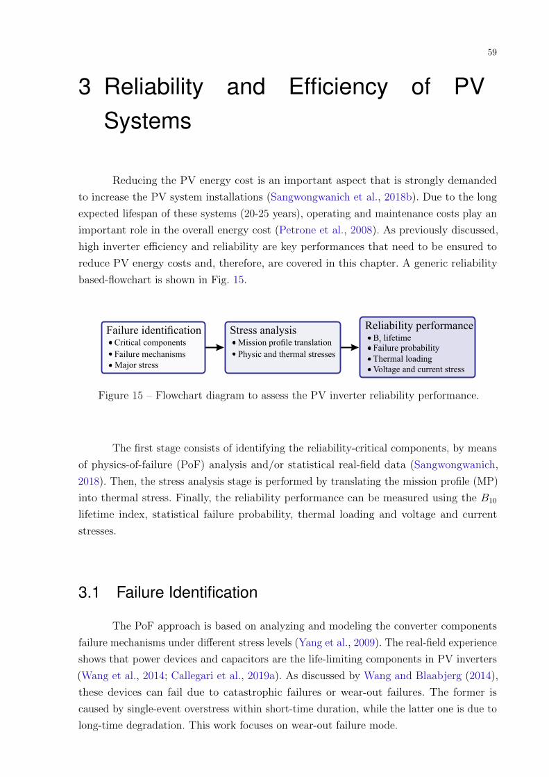
59
3 Reliability and Efficiency of PVSystems
Reducing the PV energy cost is an important aspect that is strongly demanded
to increase the PV system installations (Sangwongwanich et al., 2018b). Due to the long
expected lifespan of these systems (20-25 years), operating and maintenance costs play an
important role in the overall energy cost (Petrone et al., 2008). As previously discussed,
high inverter efficiency and reliability are key performances that need to be ensured to
reduce PV energy costs and, therefore, are covered in this chapter. A generic reliability
based-flowchart is shown in Fig. 15.
Failure identificationCritical components
Failure mechanisms
Major stress
Stress analysisMission profile translation
Physic and thermal stresses
Reliability performanceB lifetimex
Failure probability
Thermal loading
Voltage and current stress
Figure 15 – Flowchart diagram to assess the PV inverter reliability performance.
The first stage consists of identifying the reliability-critical components, by means
of physics-of-failure (PoF) analysis and/or statistical real-field data (Sangwongwanich,
2018). Then, the stress analysis stage is performed by translating the mission profile (MP)
into thermal stress. Finally, the reliability performance can be measured using the B10
lifetime index, statistical failure probability, thermal loading and voltage and current
stresses.
3.1 Failure Identification
The PoF approach is based on analyzing and modeling the converter components
failure mechanisms under different stress levels (Yang et al., 2009). The real-field experience
shows that power devices and capacitors are the life-limiting components in PV inverters
(Wang et al., 2014; Callegari et al., 2019a). As discussed by Wang and Blaabjerg (2014),
these devices can fail due to catastrophic failures or wear-out failures. The former is
caused by single-event overstress within short-time duration, while the latter one is due to
long-time degradation. This work focuses on wear-out failure mode.

60 Chapter 3. Reliability and Efficiency of PV Systems
3.1.1 PoF of Electrolytic Capacitors
There are three types of capacitors generally available for power converter applications:
aluminum electrolytic capacitors (al-caps), metallized polypropylene film capacitors (MPPF-caps)
and high capacitance multi-layer ceramic capacitors (MLC-caps). Wang and Blaabjerg
(2014) compare these technologies according to their performance from different aspects in
a qualitative way. For instance, al-caps can achieve highest capacitance and energy density
with lowest cost per Joule. Besides, the current technology of transformeless PV inverter
is based on these capacitors, being used in this work for these reasons. However, high
equivalent series resistance (ESR) and wear-out failure issues due to electrolyte evaporation
are some shortcomings of these capacitors. Tab. 3 summarizes the al-caps failure types,
failure mechanisms and critical stressors. Electrolyte vaporization and degradation of oxide
layer are the main critical failure mechanisms, while ambient temperature Ta, operating
voltage vc and capacitor ripple current stress ic are critical stressors.
3.1.2 PoF of Power Devices
Fig. 16 shows a typical power device structure composed of several layers of different
materials. Important connections to module lifetime are marked in red. There are three
dominant wear-out failure mechanisms for plastic IGBT modules (PIM) due to cyclic
thermal stress: (i) base plate solder joints cracking; (ii) chip solder joint cracking; and (iii)
bond-wire lift-off, as summarized in Tab. 3. Besides, thermal cycling is the power device
critical stressor (especially the average temperature Tavg and temperature fluctuation ∆T ).
Bond wire-
Heatsink
Base Plate
Diode IGBT
Base PlateSolder
ThermalGrease
Chip solder
Conductors
Figure 16 – Structure of a cross section of standard power device.
Since bond-wires are exposed to almost the full temperature fluctuation imposed
by the silicon power dissipation and by the wire ohmic self-heating, this study focuses on
bond-wire lift-off. Ciappa (2002), Reigosa et al. (2016) present a detailed PoF analysis of
bond-wire lift-off, whose causes are usually due to three factors:
Heel fractures: an irreversible deformation is induced by the temperature swings
and the material enters into the plastic region, leading to stress formation in the
packaging and continuous degradation;

3.1. Failure Identification 61
Tab
le3
–F
ailu
rem
odes
,cr
itic
alfa
ilure
mec
han
ism
san
dcr
itic
alst
ress
ors
ofth
ere
liab
ilit
y-c
riti
cal
PV
com
pon
ents
(Wan
get
al.,
2014
;N
ichic
on,
2020
).
Com
pon
ents
Fai
lure
sty
pes
Cri
tica
lm
echan
ism
sC
riti
cal
stre
ssor
s
Al-
caps
Cat
astr
ophic
failure
Op
en-c
ircu
itSel
f-hea
ling
die
lect
ric
bre
akdow
nan
dte
rmin
als
dis
connec
tion
Vib
rati
on,v c
Ta,i c
Shor
t-ci
rcuit
Die
lect
ric
bre
akdow
nof
oxid
ela
yer
v c,Ta,i c
Wea
r-ou
tfa
ilure
Ele
ctri
cal
par
amet
erdri
ft(C
,E
SR
,ta
n(δ
),I LC
,Rp)
Ele
ctro
lyte
vap
oriz
atio
nTa,i c
Ele
ctro
chem
ical
reac
tion
v c
Pow
erdev
ices
Cat
astr
ophic
failure
Op
en-c
ircu
itB
ond-w
ire
lift
-off
∆T
,Tavg
Shor
t-ci
rcuit
Hig
hvo
ltag
ebre
akdow
n,
hig
hte
mp
erat
ure
due
top
ower
dis
sipat
ion
and
other
s.v dc,
∆T
,Tavg
Wea
r-ou
tfa
ilure
Bon
d-w
ire
lift
-off
∆T
,Tavg
Chip
sold
erjo
int
crac
kin
g∆T
,Tavg
Bas
epla
teso
lder
join
tscr
ackin
g∆T
,Tavg

62 Chapter 3. Reliability and Efficiency of PV Systems
Wire bond lift-off: As the wire is made of aluminum (Al) and the power devices are
made of silicon (Si), mechanical stresses are induced at the Al-Si interface due to
the different thermal expansion coefficient of these two materials;
Metallurgical damage: caused by thermal stresses during the manufacturing process.
3.2 Stress Analysis
The increase in real-field experience and technological development of real-time
monitoring systems allows the availability of mission profile data from electronic power
systems. The use of real-field data allows predicting the inverter lifetime more precisely
and estimate the energy production and losses of a PV plant. Fig. 17 shows the generic
procedure adopted to translate the 1-year mission profile of ambient temperature (Ta), solar
irradiance (G) and grid voltage (vo) in device loading, including losses and temperature
profiles (Yang et al., 2011). The device lifetime under such mission profile is obtained
by applying the appropriate stress interpretation to a dedicated lifetime model. Then, a
comparison between the minimum and fixed dc-link voltage strategies can be made in
terms of efficiency, energy production and reliability.
Ambient temperature Solar irradiance Grid voltage
Mission profiles
Electrical modelLoss
Temp.
EfficiencyReliabilityassessment
System model
Efficiency
Energy yield
Tcase
. . .
Rc-h Rh-a
Ta
. . .
Pt
(Z )j-cCauer model
(Z )j-cFoster model
Pt
c
f
Tj
Cdc
Inverter
Boost
s5
d5
s1 s2
s3 s4
d1 d2
d3 d4
Topology
Lifetime
Thermal model
Thermal model
Figure 17 – Flowchart of mission profile-based approach to estimate the efficiency andlifetime of two-stage single-phase PV inverters.
3.2.1 Mission Profile Translation to Thermal Loading
The solar irradiance and ambient temperature profiles are required to estimate
the system power production during 1-year field operation, while the grid voltage profile

3.2. Stress Analysis 63
is essential to validate the minimum dc-link voltage technique at this same time. These
profiles are shown in Fig. 18 and need to be translated into the stress/loading of the
reliability-critical components. Losses on PV inverter devices are inevitable, which causes
temperature rise at some point due to their thermal impedances. The inverter electrical
model is coupled with its thermal behavior through the losses, as shown in Fig. 17.
Jan Mar May Jul Sep Nov Jan
10
20
30
40
Am
bie
nt
tem
per
ature
[ºC
]
Jan Mar May Jul Sep Nov Jan0
500
1000
1500
Sola
r ir
radia
nce
[/m
²]W
Jan Mar Ma Jul Sep Nov Jany0.95
1
1.05
Gri
d v
olt
age
[pu
]
( )a ( )b ( )c
Figure 18 – One-year mission profile of: (a) solar irradiance, (b) ambient temperature and(c) grid voltage.
The junction-to-case thermal impedance (Zth(j−c)) of power devices can be modeled
as a Cauer RC network, which reflects in the physical-material-based representation of the
impedance (Wintrich; Nicolai; Tursky, 2015). The circuit nodes allow to access the internal
temperatures of each layer of the semiconductor device, as observed in Fig. 19(a). On
the other hand, the Foster RC network does not have any physical representation, being
a fitting of the temperature transient curve provided by the manufacturers. Thus, the
thermal parameters are found in datasheets and this configuration is shown in Fig. 19(b).
The analytical expression of Foster-based thermal impedance is described as:
Zth(j−c)(t) =n∑
i=1,2,3,4Rthi(1− e−t/τi), (3.1)
where Rthi represents the thermal resistance of the device layers. The first one determines
the steady-state mean junction temperature Tjm and the second dictates the dynamic
behavior of the junction temperature Tj, according to the time constant τi, defined by:
τi = RthiCthi, (3.2)
where Cthi is the thermal capacitance of the device layers. Tab. 4 shows the thermal
parameters of IKW40N60H3 power device from Infineon. Since the case temperature Tc
dynamic response is slow, the thermal capacitance of Zth(c−h) is neglected (Andresen et al.,
2015). Ma (2015) proposes an improved thermal model, which combines the advantages
of both models. The power device losses Pt are applied to the thermal model depicted
in Fig. 20(a), which is based on the Cauer circuit to estimate the case temperature and

64 Chapter 3. Reliability and Efficiency of PV Systems
Tcase
Pt
(Z )th(j-c)Cauer model
(Z )th(j-c)Foster model
Pt
c
f
( )a
Rth1
Cth1
Rth2
Cth2
Rth3
Cth3
Rth4
Cth4
Tcase
Tjm
Tjm
Rth1
Cth1 Cth2 Cth3 Cth4
Rth2 Rth3 Rth4
( )b
Figure 19 – Thermal impedance models: (a) Cauer-model. (b) Foster-model.
Table 4 – Foster thermal impedance for IKW40N60H3 power module from Infineon.
Thermal impedanceZth(j−c) Zth(c−h)i = 1 i = 2 i = 3 i = 4
IGBTRthi (K/W) 0.025 0.092 0.130 0.189 0.7
τi (s) 1.3×10⁻⁵ 1.3×10⁻⁴ 1.4×10⁻³ 1.83×10⁻² 0
DiodeRthi (K/W) 0.339 0.444 0.581 0.135 0.7
τi (s) 1.3×10⁻⁴ 1.5×10⁻³ 1.82×10⁻² 9.21×10⁻² 0
feed it into the Foster thermal circuit, in order to obtain a better estimate of the junction
temperature.
Regarding al-caps, the ESR ohmic losses are computed for each frequency component
of the capacitor current ic spectrum, since ESR is a function of frequency and temperature.
Both factors contribute to the wear-out failure mechanisms in aluminum electrolytic
capacitors, by increasing ESR over time (Buiatti et al., 2011; Wang et al., 2018). The
relationship between the al-cap losses Pc and its hot-spot temperature Th is described by
the simplified thermal model of Fig. 20(b), unlike the complex multi-layered thermal model
of power devices. The hot-spot temperature is estimated through the thermal resistance
Rthc and ambient temperature. Accordingly:
Th = Ta +Rthc
look−up table︷ ︸︸ ︷∑h
ESR(hfn, Th)i2c(hfn), (3.3)
where h is the harmonic order, ESR(hfn, Th) is the equivalent series resistance at

3.2. Stress Analysis 65
ESL
ESR...
u2
u2
ESR(f,T )h
ic1
icn
FFTic
Rthc
Cthc Ta
Th
Pc
ic
Pco
Psw
Tcase
. . .
Rc-h Rh-a
Ta
. . .
Pt
(Z )j-cCauer model
(Z )j-cFoster model
Tj
Pt
c
f
Electrical model Thermal model
Pc
Power device
Pt
Al-Caps
( )b
(a)
Losses evaluation
Figure 20 – Simplified thermal model of (a) power devices and (b) al-caps, from theelectrical domain to thermal domain linked by power losses.
frequency hfn and at hot-spot temperature and, finally, ic(hfn) is the RMS-value of
the ripple current at frequency hfn. Losses are estimated for each MP point by means of 4
dimensions look-up tables, whose input parameters are: Ta, G, vo and the feedback junction
temperature/hot-spot temperature. The look-up tables of al-caps and power devices are
built according to Wang et al. (2019) and Callegari et al. (2019b); and are shown in Fig. 21
for fixed and minimum dc-link voltage strategies.
The loss look-up tables shown in Fig. 21 are used to estimate losses on devices
during 1-year field operation, through the input MP shown in Fig. 18. As noted for the
proposed technique, losses are lower for all semiconductors and al-caps, except for the boost
diode. The minimum dc-link voltage operation reflects in the increase of the boost diode
current and consequently in its losses, since the power processed by the converter is the
same for both techniques. Moreover, the difference between the losses of the proposed and
traditional technique is reduced with the increase of the grid voltage, since the minimum
dc-link voltage increases for the converter to remain grid-connected.
3.2.2 Thermal Cycling Interpretation
The thermal loading translated from the mission profile needs to be analyzed in
order to determine the thermal cycling information, as indicated in the flowchart of Fig. 22.

66 Chapter 3. Reliability and Efficiency of PV Systems
G [W/m²] v [pu]o
G [W/m²] v [pu]o
G [W/m²] v [pu]o
G [W/m²] v [pu]o
Proposed
Traditional
Traditional
Proposed
Proposed
Proposed
Traditional
(a) (b) ( )
(e)
c
T = 30ºCa
T = 30ºCa
T = 30ºCa T = 30ºCa
G [W/m²] v [pu]o
Proposed
Traditional
T = 30ºCa
G [W/m²] v [pu]o
(d)(f)
Traditional
T = 30ºCa
Proposed
Traditional
Figure 21 – Power devices and al-caps total losses, considering different solar irradianceang grid voltage conditions: (a) Inv. IGBTs and (b) inv. diodes. (c) Dc-linkcapacitor (partnumber B43630C5397M0 from TDK). (d) boost IGBT and (e)boost diode. (f) Boost capacitor (partnumber B43630C5397M0 from TDK).
The thermal loading of power devices is affected by two time constants: (i) thermal
long-cycles (related to weather variations) and (ii) thermal short-cycles (due to grid
frequency) (Ma et al., 2015). The rainflow counting algorithm is employed to find the heating
time (ton), junction temperature fluctuation (∆Tj) and average junction temperature
(Tjm) in thermal long-cycles (Huang; Mawby, 2013). As short-cycles are well-defined, the
analytical approach of Ma et al. (2015) is applied to calculate the junction temperature
fluctuation of the thermal loading due to the grid frequency, while Tjm is given by the
thermal model output and ton is set to 1/120 s.
The analytical evaluation of short-cycles junction temperature fluctuation is not a
trivial task. Ma et al. (2015) approximate the device loss waveforms by a known waveform
defined by a sum of two-square pulses, with the same original loss area. This result is
shown in Fig. 23(a) for two different levels of processed active power. In such case, the time
when Tj is maximum is determined at t2, in order to calculate ∆Tj. Once the steps times
are set at t1 = 1/(8fn), t2 = 3/(8fn) and t3 = 1/(2fn), junction temperature fluctuation
is analytically determined by (Ma et al., 2015; Ma; Blaabjerg, 2012):
∆Tj ≈ PtZth(j−c)
(t2 = 3
8fn
)+ 2PtZth(j−c)
(t2 − t1 = 1
4fn
). (3.4)
The approximate approach shows an acceptable consistency with the real junction

3.2. Stress Analysis 67
Mission Profile
Power Losseslook-up table
TaG
Thermal Model
Ploss
Tj
computation
Tjm ΔTjton
Tj
Mission Profile
Power losses and voltage
look-up tables
Thermal Model
Ploss
Th
TaG
vcTh
Capacitors:Power Devices:
Long and Short-cycles
L = L v 2c 0 c
Vc( (-n T - T0 h
10
((
LC = Σ T sL c,kk
α (β ∆T +β ) γN = A(∆T ) ar C+(t )f j on
C+1( (01 j exp( (Ea
k Tb jm
fd
( (
Lifetime model:
LC = + Σ 1 Nf k k
f T n s
Nf k
MR:
Lifetime model:
MR:
LNf
vo vo
Figure 22 – Flowchart for the reliability evaluation of power devices and capacitors.
temperature fluctuation when the converter is processing only active power, as depicted in
Fig. 23(b). It is worth to remark that this methodology should not be applied when the
converter performs harmonic current compensation, as discussed by Barros (2019).
Then, the accumulated damage can be estimated over one year. The lifetime model
presented by Scheuermann, Schmidt and Newman (2014) is applied to evaluate the wear-out
failures due to bond-wire lift-off:
Nf = A (∆Tj)α ar(β1∆Tj+β0)(C + (ton)γ
C + 1
)e
(Ea
kbTjm
)fd, (3.5)
where Nf is the number of cycles to failure for each MP stress condition and ar is the
bond-wire aspect ratio. fd is defined as 1 for IGBT and 0.6204 for diode. The other
parameters are described in Tab. 5.
Regarding al-caps, a widely used capacitor lifetime model is employed for their
reliability prediction (Wang; Blaabjerg, 2014):
Lc = L0
(vcVc
)−n2(
T0−Th10
), (3.6)

68 Chapter 3. Reliability and Efficiency of PV Systems
Po
wer
lP
[pu
]o
sses
tT
°C[]
j ∆Tj
Time s[ ]ton1
∆Tj
1
2
Real
t1t2
ton2
( )a
(b)
t3 Time s[ ]Tn
Tn
(MA et al.,2015)
Processed power: 1 pu Processed power: 0.5 pu
Processed power: 1 pu Processed power: 0.5 pu
Figure 23 – Pulsed losses in power devices: (a) real loss and approximate loss by asum of two-square pulses. (b) Corresponding real and approximate junctiontemperature.
Table 5 – Lifetime model parameters and their experimental test limits.
Parameter Value Experimental conditionA 3.4368 × 10¹⁴
64 ≤ ∆Tj ≤ 113 Kα -4.923B1 -9.012 × 10⁻³
0.19 ≤ ar ≤ 0.42B0 1.942C 1.434
0.07 ≤ ton ≤ 63 sγ -1.208fd 0.6204
32.5 ≤ Tj ≤ 122 CEa 0.06606 eVkb 8.6173324 × 10⁻⁵ eV/K
where Lc and L0 are the lifetime in hours under operating and testing conditions,
respectively. vc and Vc are the al-caps voltage under operating and testing conditions. T0 is
the temperature under test condition. n = 3 refers to the voltage stress exponent, defined
between 1 and 5. Then, the damage is accumulated linearly and independently in both
components using the Miner’s rule (MR) (Sangwongwanich et al., 2018b), given by:
LC′ =
∑k
long−cycles︷ ︸︸ ︷
1Nfk
+
short−cycles︷ ︸︸ ︷fnTs,MP
Nfk
(3.7)

3.3. Reliability Evaluation 69
LC′ =
∑k
Ts,MP
Lc,k, (3.8)
where (3.7) and (3.8) are the MR equations for power devices and capacitors, respectively. k
is the number of 1-year samples and Ts,MP = 60 s is the MP sampling time. LC is the total
1-year static lifetime consumption and indicates how much lifetime of the component has
been consumed during the operation. The component is considered to reach its end-of-life
when the LC is accumulated to 1.
3.3 Reliability Evaluation
With the previously estimated stress conditions, the components reliability performance
can be evaluated. For a PV system with several components, statistical tools to map
the component-level reliability performance to the system-level reliability performance is
required (Sangwongwanich, 2018).
3.3.1 Monte-Carlo Simulation
The 1-year damage accumulation is fixed, using the previous lifetime models.
However, this approach is far from reality, since deviations from model parameters are
not considered and the time to the end-of-life of critical components can vary within a
range due to different thermal stress experiences over the years in real-field operation
(Sangwongwanich et al., 2018a). Therefore, a statistical approach based on Monte-Carlo
simulation is conducted according to the steps indicated in Fig. 24.
Equivalent static
values
ΔTj
Tjm
ton
LC’
LC’ Vc Th
Monte-Carlo
simulation
ΔTj
Tjm
‘
‘
Vc
‘
Th
‘
Time
Th
Time
Tj
...
samples
Time
f(x)
Time
F(x
)
Weibull PDF: f(x)
B10
Weibull CDF: F(x)
CapacitorSemiconductor
n
n samples
Parameter
PD
F
μ
CI=99%
Figure 24 – Flowchart of Monte-Carlo simulation for power devices and capacitors.
The stochastic parameters of the lifetime models (vc, Th, ton, ∆Tj , Tjm) are converted
into static equivalent ones (v′c, T
′h, t
′on, ∆T ′j , T
′jm), in order to obtain the same LC
′previously

70 Chapter 3. Reliability and Efficiency of PV Systems
estimated. Then, lifetime models variations are introduced, modeled by normal distribution
with a 99 % confidence interval.
Subsequently, the Monte-Carlo analysis is simulated for n = 5000 samples and the
result is fitted using Weibull probability density function (PDF) f(x) (Zhou et al., 2016),
given by:
f(x) = β
ηβxβ−1exp
−(xη
)β , (3.9)
where η is the scale parameter, β is the shape parameter and x is the operation time
(Sangwongwanich et al., 2018a). All these parameters are estimated for a maximum
likelihood with the Weibull distribution. The component unreliability is represented by
the cumulative density function F (x) (CDF), given by the PDF area, as:
F (x) =∫ x
0f(x)dx. (3.10)
On the other hand, the system wear-out failure probability is obtained with the
series-connected reliability model, given by:
Fsys(x) = 1− [1− Fi(x)]ni [1− Fd(x)]nd [1− Fc(x)]nc , (3.11)
where Fi(x), Fd(x) and Fc(x) are the unreliability functions of the ni IGBTs, nd diodes
and nc capacitors, respectively. Besides, (3.11) considers that all devices converge to the
same CDF. Finally, the time when 10 % of the samples have failed is called B10, an index
used as a metric to the system reliability assessment.
3.4 Efficiency Assessment
The converter efficiency analysis is based on the estimation of individual loss in its
stages. The loss evaluation consider the semiconductors, inductors and capacitors. The
modeling of the power devices conduction and switching losses can be done via different
approaches. For sake of simplicity, the loss modeling is attained by means of 4 dimension
look-up tables, developed based on information from manufacturers’ datasheets. The
al-caps loss look-up table is developed as explained in the previous section, using the
ESR approach as a function of harmonic current order according to the manufacturers’
datasheets.
The losses of magnetic components consist of the core loss and the winding loss.
The powder cores and the windings are designed according to the guidelines presented
in Cota (2016), with respect to the number of parallel wires, stored energy requirement,

3.5. Chapter Closure 71
effective area AL, maximum magnetic flux density Bmax (does not exceed 70 % of the
flux density that saturates the core), maximum current and number of turns NL. The
contributions of proximity and skin effects are disregarded. Powder cores of the High Flux
family from Magnetics are employed, since these materials have air gaps with notable
characteristics for applications in electronic power converters, such as: low hysteresis and
eddy current losses and excellent inductance stability under both dc and ac conditions
(Magnetics, 2020). Then, the improved generalized Steinmetz equation (iGSE) (Jieli Li;
Abdallah; Sullivan, 2001) is used to estimate the core loss for non-sinusoidal signals and
the winding loss is obtained considering the windings equivalent series resistance, according
to Fig. 25.
PL,core
L
R
iL
+
_
vL
iL
vL
RMS u²
R
PL,w
(.) dt∫ (A N )L L-1
BL
iGSEα , β , k
L L
Inductor core loss:
Inductor winding loss:
...
Electrical model
PL
G
Ta
vo
L
Power loss look-up table
Figure 25 – Procedure for assembling the core and windings loss look-up table of magneticcomponents.
Once the converter losses are computed, the European efficiency index (EF) is
used to compare the performance of both techniques. It consists of the average operating
efficiency referenced in practically all inverters datasheets (Pearsall, 2017):
(3.12)EF = 0.03η5% + 0.06η10% + 0.13η20% + 0.1η30% + 0.48η50% + 0.2η100%,
where ηz% is the efficiency at z % of inverter rated power. On the other hand, the European
efficiency gain GEF is given by:
GEF = EFp − EFt, (3.13)
where EFp and EFt are the EF for the proposed and traditional techniques, respectively.
3.5 Chapter Closure
In this chapter, the PV system reliability methodology was introduced based
on real-field mission profile, where the failure identification, mission profile translation

72 Chapter 3. Reliability and Efficiency of PV Systems
to thermal loading, thermal cycling interpretation, lifetime evaluation and reliability
performance are involved. Monte-Carlo simulations introduce statistical values in the PV
inverter reliability, such as: unreliability function, failure distribution and B10 lifetime
(metrics to the system reliability assessment). Then, the efficiency evaluation was introduced
and a brief description of magnetic components design was performed. European efficiency
was indicated as an efficiency metric to compare the inverter operation with fixed and
minimum dc-link voltage.

73
4 Experimental Aspects and Case Study
The increasing availability of low-cost and high-performance digital signal processors
stimulates the diffusion of digital controllers. From this standpoint, the application of digital
control techniques to power converters play a very significant role, which indicates the
need for research efforts towards digital control applications. Thus, this chapter introduces
some practical aspects of implementing digital control in power inverters, as well as the
experimental setup description used to validate the minimum dc-link voltage strategy. The
procedures for conditioning the test bench is also addressed. The final part of this chapter
is dedicated to the mitigation of dc-current injection into the grid by the inverter, which
can result in serious damage to the electrical power system.
4.1 Experimental Setup
The experimental setup used to develop this research is shown in Fig. 26(a). The
Supplier FCCT400-50-iF15451 PV array emulator supplies the voltage to the inverter
dc-side. Due to the equipment limitations, the experimental and reliability-simulated
results employ different PV module part number with different power ratings. The Supplier
FCAT450-22-15 grid emulator is connected to the inverter ac-side, which can produce
different types of voltage disturbances. The voltage and current measurements are obtained
from a Tektronix DPO 2014B oscilloscope equipped with A612 and P5200A probes.
Fig. 26(b) shows the top view of the PHB two-stage single-phase commercial inverter,
highlighting the main power circuit components and signal conditioning. It is worth to
remark that the power devices are in direct contact with the heatsink through proper
thermal grease and are welded to the plate underneath.
The minimum dc-link voltage control strategy is programmed in the Texas Instruments
@60 MHz TMS320F28034 fixed-point digital-signal processor, as depicted in Fig. 26(c).
As observed, several components are required to allow proper operation of the commercial
converter. DSP is the core of the inverter, being responsible for controlling both power
stages. All peripheral circuits required to implement the proposed control structure are
present in this DSP, namely: 12-bits analog-to-digital converters (ADC), PWM unit and
digital input/output (I/O) pins.
Converter controlled operation requires measurement of many electrical analog
variables, such as: voltage and current of the PV array, dc-link voltage, output current,
output voltage and PCC voltage. The acquisition of these signals requires adequate
conditioning electronic circuits, filtering capability and signal scaling. Regarding this topic,
two concerns must be noted: (i) The sensor signal is scaled to fully exploit the ADC

74 Chapter 4. Experimental Aspects and Case Study
vpvipv
dc
dc
CpvCdc
vdc
ac
dc
voioBoost conv. Inverter LCL filterPV array
Grid
Zg
DSP
Relay
s1
vg
PowerSupply
+3.3V+5V_+12V_...
_
Analog signals conditioning,
scaling and offset
ipv vpv vdc io vo vg
ADC
TMS320F28034
PWM I/O
0-3.3V...
EP
WM
2A
EP
WM
2B
EP
WM
5A
EP
WM
5B
EP
WM
1A
Power devicedrivers
+12V_
Additional analogsignals
s 1 s 2 s 3 s 4 s 5
s1-4
Add
itio
nal
digi
tal
I/O
Rel
ays
Dri
vers
Sta
tus
...
JTA
G
CCS 6.1
s5
+12V_
PC
Oscilloscope Tektronix DPO 2014B
Command and protection circuits
Single-phase inverter
Grid emulator PV array emulator
24
3
1
5
6
(a)(b)
( )c
dc-side ac-side
Figure 26 – (a) Experimental setup. (b) PV inverter components: 1) boost capacitor,2) boost inductor, 3) dc-link capacitor bank, 4) filter inductors, 5) filtercapacitor, 6) conditioning electronic circuits. (c) Schematic of connectionbetween hardware and DSP.
voltage range (0 - 3.3 V), maximizing the number of effective bits of the analog signal
representation in digital domain; (ii) Application of 1.65 V offset on ac-nature signals,
since the ADC does not accept negative voltage values.
Another important design criterion of commercial inverter is its operation as a
standalone unit, i.e., regardless of external power supplies. As observed in Fig. 26(c), the

4.1. Experimental Setup 75
power supply of the instrumentation circuits is obtained from the input dc-side stage,
using a fly-back converter and voltage regulators. From a development point of view, the
commercial inverter is few flexible to perform tests of the control algorithms due to three
reasons: (i) It is a finished product, tested, debugged and ready for commercialization,
which complicates the firmware development process; (ii) Algorithm debug is only possible
by energizing the dc-input with at least 80 V; (iii) The DSP pins are all welded and no
test points for oscilloscope probes are available; (iv) TMS320F28034 DSP has very limited
processing capacity and memory, which requires creativity and a considerable C-language
knowledge for code optimization. All of these limitations make the development of this
research more challenging.
The power devices are driven by a suitable control circuit, allowing them to be
switched from the on to off -state and vice-versa. They are controlled by PWM signals
generated from the DSP ePWM modules. In practice, logically complementary gate signals
implemented via PWM modulator is not sufficient to avoid driving devices simultaneously
on the same converter arm. Effective protection against these issues is implemented by
introducing switching dead-times before the application of turn-on signal to the gate. This
research considers a switching dead-time of 1.5 µs to avoid short-circuit in the dc-link
capacitor bank.
Regarding communication with desktop PC, the DSP is programmed and debugged
via a JTAG port. The XDS 100v2 JTAG controller is the debugger used to perform this
task. Code Composer Studio (CCS) software from Texas Instruments is used for algorithm
development, debugging and online visualization of the desired variables from the running
code in the DSP. Moreover, some digital output signals are used for controlling relays and
status LEDs for safety concerns.
Once the structure and components of the experimental setup are described, Tab. 6
shows the main parameters of the single-phase grid-connected PV system, as well as the
partnumbers of power devices, magnetic components and al-caps. It is reinforced that the
reliability and efficiency analyzes are obtained considering the PV array shown in Tab. 6
to better cover the converter power rating. On the other hand, the experimental results
are obtained using 20 series-connected PV panels, partnumber KM(P)50, due to the test
bench limitations. The operating conditions of solar irradiance and ambient temperature
are easily configurable during experimental tests, which guarantees flexibility in the MPP
voltage and current configuration. Also, all controller gains are shown in Tab. 7.
It is noteworthy that the dc-link voltage controller gains were obtained considering
a fixed dc-link voltage of 385 V for both strategies. This simplification is possible since
the dc-link voltage variations oscillate around this value and no control performance
degradation is observed for the proposed strategy. Therefore, adaptive gain calculations
are not demanded.

76 Chapter 4. Experimental Aspects and Case Study
Table 6 – Parameters of the single-phase grid-connected PV system.
Parameter Label ValuePV array rated power (JKM330PP) Pmpp 3.3 kW (5 × 2)Boost inductance (Magnetics 58617) Lb 980 µHBoost internal resistance Rb 38.65 mΩBoost/inverter switching frequency fsw 20 kHzSampling frequency fs 40 kHzLCL filter inductance (Mag 58907) Lf , Lg 2 mHLCL filter internal resistance Rf , Rg 77.10 mΩLCL filter capacitance Cf 3.3 µFGrid voltage (RMS) Vo 220 VGrid fundamental frequency fn 60 HzGrid angular frequency ωn 377 rad/sFixed dc-link voltage v∗dcf 385 VPower devices (IKW40N60H3) s1−5, d1−5 40 A/600 VDc-link capacitor (B43630C5397M0) Cdc 390 µF (1 × 3)Dc-link capacitor ESR ESRdc 320 mΩBoost capacitor (B43630C5397M0) Cpv 180 µF (1 × 1)Boost capacitor ESR ESRpv 660 mΩHeatsink thermal resistance Rh 0.5 K/WCapacitor thermal resistance (Wang et al., 2019) Rthc 6 K/W
Table 7 – Controller gains of the single-phase grid-connected PV system.
Parameter Label ValueInner loop: proportional gain kp,c 30 ΩInner loop: integral gain ki,c 37 Ω/sInner loop: resonant gain kr,c 2000 Ω/sdc-link voltage outer loop: proportional gain kp,dc -0.311 Ω−1
dc-link voltage outer loop: integral gain ki,dc -2.672 Ω−1/sReactive power outer loop: proportional gain kp,q -0.016 V −1
Reactive power outer loop: integral gain ki,q -0.505 V −1/sSRF-PLL: proportional gain kp,pll 50.755 V −1/sSRF-PLL: integral gain ki,pll 0.571 V −1/s2
Boost converter control: proportional gain kp,b 0.001 Ω−1
Boost converter control: integral gain ki,b 0.08 Ω−1/s
4.2 Test bench conditioning procedures
This section briefly covers the procedures for conditioning the test bench in Fig. 26.
The goal is to experimentally validate all stages of the converter control hierarchy, before
implementing the minimum dc-link voltage control strategy. The validations of the control
stages are developed individually in the following order:
Grid synchronization algorithm: Fig. 27(a) shows the SOGI-PLL behavior under a 30
% grid voltage step. Since the fundamental frequency is set to 60 Hz, the estimated

4.2. Test bench conditioning procedures 77
v [230 V/div]d
-1ω [228 rad.s /div]
Grid voltage step
(a)
t [20 ms/div]
θ [3.8 rad/div]
20 25 30 35 40Frequency [kHz]
0
10
20
30Zoomed view: Spectrum
Syn
thes
ized
vol
tage
[V
]
2fsw
t [20 ms/div]
io
vs
Current step
vo
vdc
igio
(b)
( )
t [10 ms/div]
c
Figure 27 – (a) Experimental results of grid angle amplitude and angular frequencyestimated by SOGI-PLL, normalized from 0 to 3.3V (rated TMS320F28034DSP voltage output). (b) Experimental waveforms of the injected current anddifferential voltage synthesized by the converter, using a unipolar modulationstrategy (vs [250 V/div]; io [2 A/div]; and time [20 ms/div]). Zoomedview in the high-harmonic frequencies voltage spectrum is also showed. (c)Experimental steady-state results of the current-controlled PV inverter (vo[250 V/div]; vdc [250 V/div]; io and ig [10 A/div]; and time [10 ms/div]).
angular frequency ω converge to 377 rad/s as expected, regardless the grid voltage
variation.
Unipolar modulation strategy : Fig. 27(b) shows the differential voltage synthesized by
the converter with three voltage levels for unipolar modulation and the output current
io during a transient event. As noted in the zoomed view, the voltage high-frequency
spectrum is allocated to double of switching frequency (2× 20 kHz), indicating less
filtering requirements and less bulky and cheaper inductors. The current has low
harmonic distortion, even with low power being processed by the converter connected
to the 220 V RMS grid.
Inner current loop: The current control dynamic is shown in Fig. 27(b), during an
amplitude current step from 1 A to 3 A. The closed-loop time response is low, since the
output current reaches the reference almost instantly (indicating a well-designed PR
controller). Also, Fig. 27(c) shows the steady-state behavior of the current-controlled
PV inverter. The current amplitude reference is set to 5 A and the dc-link voltage is

78 Chapter 4. Experimental Aspects and Case Study
fixed, powered by a conventional dc source. Qualitatively, a low-harmonic distortion
is noted in this result.
Finally, experimental tests are performed to validate the cascade-control structure,
as shown in Fig. 28. The dc-stage and MPPT algorithm are disabled in these tests, which
indicates that the PV array voltage is directly applied to the dc-link capacitor bank.
The dc-link voltage reference can be freely assigned, as long as the minimum connection
voltage is reached and this operating point exists on the PV array curve under the
emulated ambient conditions. These tests are performed with an emulated PV array of
20 series-connected panels partnumber KM(P)50 (50-W power rating from manufacturer
Komaes Solar), operating under 25 C and solar irradiance between 300 and 500 W/m2.
Fig. 28(a) shows the grid connected inverter with dc-link voltage close to the
array open-circuit voltage (drained current ipv is zero). The dc-link reference is set to
approximately 400 V and the converter power factor (PF) is not close to the unit. An
approximately constant non-characteristic oscillation in the fundamental frequency is
observed in the dc-link voltage ripple, possibly caused by intrinsic asymmetries in the
switching behavior of power semiconductor devices, imparities in gate driver circuits, device
turn-on and turn-off delays, nonidentical device voltage drops and sampling biases from
the ac-current and ac-voltage sensors. This characteristic is evident when the converter
processes low levels of active power (Yan et al., 2015) and is covered in the next sections.
Fig. 28(b) shows the grid connected inverter, with dc-link voltage controlled at the
360 V and the array operating at 300 W/m2 and 25 C. Greater power is extracted from
the PV array compared to the previous case. The injected current amplitude increased from
920 mA to 2 A and the 60 Hz component in the dc-link voltage ripple is reduced. Then,
the solar irradiance is increased from 300 W/m2 to 500 W/m2, with the dc-link voltage
reference still set at 360 V (vide Fig. 28(c)). The injected current amplitude increased
from 2 A to 3 A, as well as the active power drained from the panels. Besides, a 120
Hz ripple in the dc-link voltage is evidenced, which suggests the use of a MAF tuned to
this frequency with the purpose of improving the PI-controller tracking. Figs. 28(e) and
(f) show, didactically, the array I-V and P-V operating points calculated by the control.
Finally, Fig. 28(d) shows the dc-link voltage dynamics, when the voltage reference is
changed from 400 to 360 V. Despite the disturbance, the system remains well-controlled
and stable.
4.3 Practical Aspects of Digital Implementation
This section briefly covers some features of the digital control implementation in
commercial converter. Nowadays, two DSP architectures are found, separated according
to their arithmetic units: floating point and fixed point. The former is favored where the

4.3. Practical Aspects of Digital Implementation 79
120 Hz
(b)
(f)
(d)( )c
dc-link voltage ripple
Injected current
Grid voltage
100 200 300 4000
1
2
PV
arr
ay c
urre
nt i
[A
]pv
300 W/m² 500 W/m²
0 100 200 300 400
PV array voltage v [V]pv
0
200
400
PV
arr
ay p
ower
P[W
]pv
0
PV array voltage v [V]pv
(a)
dc-link voltage ripple
Injected current
Grid voltage
dc-link voltage
Injected current
400→ 360V
400
300 500 W/m²
360 V
300 500 W/m²
400 360 V
(e)
dc-link voltage ripple
Injected current
Grid voltage
t [1 s/div]t [10 ms/div]
t [10 ms/div] t [10 ms/div]
120 Hz
Figure 28 – Cascade-control performance of single-phase PV inverter. Dc-link voltagecontrolled at (a) 400 V and (b) 360 V, with PV array operation under 300W/m2 and 25 C. (c) Dc-link voltage controlled at 360 V and PV arrayoperation under 500 W/m2. (d) Dc-link voltage control dynamics, when thevoltage reference is changed from 400 to 360 V. (vo [250 V/div]; io [2 A/div];vdc [100 V/div]; vdc ripple [1 V/div] and time [1000 and 10 ms/div]). Array (e)I-V curve and (f) P-V curve operating points calculated by the control whendisturbances are performed.
computational demand is high. Floating-point processors manipulates rational numbers
via a minimum of 32 bits with high performance and precision, representing that number
with a mantissa and an exponent similarly to scientific notation (Marafao, 2004). However,
these processors are rare in industrial field, since the cost of such units is beyond the
maximum affordable for typical PV converter application (Buso; Mattavelli, 2015).
On the other hand, fixed-point DSPs are widely used in power electronics and
mostly work with 16-bit or 32-bit resolution, yielding up to 216 and 232 possible bit
patterns, respectively. Unlike floating-point DSPs, the quantized values are equally spaced
across the whole range, which leads to higher quantization errors and lower precision. The

80 Chapter 4. Experimental Aspects and Case Study
arithmetic quantization error consists of the finite precision effect that characterizes the
logical unit used to compute the inverter control algorithm. This precision determines the
need for truncating and rounding the variables according to the available number of bits.
The designer main challenge is to prevent the result of multiplying or adding fixed-point
variables from exceeding the designated number of bits. Rounding caused by overflow
or underflow leads to distortion of controllers frequency response, impairing the system
achievable performance.
Texas Instruments has developed a collection of high-precision and optimized
functions for C language programmers to seamlessly port a floating-point algorithm into
fixed-point code (Texas Instruments, 2010). In this format, the binary point that separates
the integer part from the fractional part is displaced, increasing the variable representation
range at the expense of resolution/accuracy. As the inverter digital control is implemented
with a 32-bit fixed-point DSP, some additional precautions must be considered when using
the IQmath library:
Normalize control variables whenever possible to improve the number accuracy in
fixed-point representation ( iq30, as presented in Appendix. A);
As shown in Tab. 8 of Appendix. A, the variable is declared according to its value
range. For instance, the angular frequency wn estimated by SOGI-PLL must be
declared as iq22 to avoid overflow and use the best available accuracy.
Variables susceptible to sudden changes during transient events are output limited
to avoid the occurrence of overflow. For instance, PI controller is implemented with
anti-windup to limit the integrator calculation during transient events;
The data type definition must take into account the minimum and maximum
operating range and the variable accuracy. A trade-off is observed between both
characteristics: precision decreases as the range increases;
The designer must know the magnitude order of the multiplications, divisions, sums
and subtractions between different variables to define the data type and to avoid
overflow situations;
To optimize the control algorithm processing, avoid making unnecessary calculations.
For instance, defining a constant equal to 6.283185307 instead of calculating the
product 2π.
TMS320F28034 DSP has 45 pins for general purpose I/O (GPIO). These pins are
multiplexed and can be individually selected to operate as digital I/O or connected to
the ePWM module via GPxMUXn register configuration. After proper configurations
4.4. Dc-component Mitigation in PV Inverters 81
according to the manufacturer datasheet (Texas Instruments, 2018), the implementation of
double update PWM mode is performed through triangular carrier (up-down-count mode
selected by the time-base control register TBCTL). The interruption is requested twice
during the modulator period in this PWM mode, reducing the system response delay. In
such case, the sampling frequency fs is equal to twice the modulator/switching frequency
fsw, while sampling and switching process are properly synchronized. This last fact allows
the signal to be sampled on the average of the continuous signal, which is exactly what
has to be controlled (Hoffmann; Fuchs; Dannehl, 2011; Buso; Mattavelli, 2015). Several
other registers are configured for the suitable configuration of the DSP pins and internal
modules. Describing all of them is not the purpose of this section, since these topics can
be found very detailed in the TMS320F28034 technical manual.
With the digital modulator properly configured, it is convenient to derive a digital
controller from an analog controller project. This process is called virtual controller
discretization and requires minimal knowledge of digital control theory to be applied
successfully. Thus, this work employs the Tustin with prewarping and Trapezoidal discretization
methods for the PR and PI controllers, respectively (Yepes, 2011).
4.4 Dc-component Mitigation in PV Inverters
Although providing galvanic isolation and ensuring null dc-current injected in the
grid, the presence of bulky, heavy and expensive low-frequency transformers reduces the
PV system efficiency. As discussed in previous chapters, transformerless inverters has been
widely used to improve the PV systems performance. For instance, Calais, Agelidis and
Dymond (2001) verified a 25 % cost reduction between traditional and transformerless
PV systems. However, some shortcomings appear when the transformer is removed, such
as: dc-current injection at the inverter output (Buticchi; Lorenzani; Franceschini, 2011),
ground leakage current due to common-mode voltage and parasitic capacitance (Lopez
et al., 2010; Figueredo, 2015) and the voltage-level mismatch between the inverter and
grid (Koutroulis; Blaabjerg, 2013). Among these concerns, the dc-component injection
can affect the system operation, causing line-frequency ripple in the dc-link voltage and a
further second-order harmonic in the ac current.
In grid-connected PV inverters, the dc-component injection can be generated by
the following sources (LEM, 2004; Masoum; Moses, 2010; Yan et al., 2015):
Small differences in semiconductor intrinsic characteristics, including on-state resistance
and on-state forward voltage;
The switching process is affected by the on-off switching delay between PWM signals
of power devices in the same arm;

82 Chapter 4. Experimental Aspects and Case Study
Offset in the measurement from the ac-current and ac-voltage sensors.
Moreover, as discussed by Ahfock and Hewitt (2006), Masoum and Moses (2010)
and Yan et al. (2015), dc-component injection can cause negative effects on the electrical
power system (EPS):
Dc component can circulate between inverter arms or among inverters in a paralleled
configuration, increasing the system losses.
Dc-component injection can affect the regular operation of grid-connected loads,
especially ac motors;
The corrosion of grounding wire in electrical substations is intensified due to the dc
component;
The core of transformers are driven to unidirectional saturation as a consequence of
dc-current injection in the grid. The transformer time to the end-of-life is reduced as
a result of increased hysteresis and eddy current losses and noise.
Due to EPS power quality concerns, IEC 61727 suggests dc-current injection limits
less than 1 % of the rated output current (IEC, 2004). Moreover, transformerless PV
inverter must disconnect from the grid if dc-offset current injection exceed 0.5 % of the
rated output current, according to the IEEE standard 1547-2003 guidelines (IEEE, 2003).
Accordingly, several strategies are proposed in the literature to mitigate the dc-current
injection, which can be classified into passive and active methods. The insertion of coupling
transformers and blocking capacitors on the inverter dc- or ac-side are passive solutions
(Berba; Atkinson; Armstrong, 2012), which are unattractive due to the setup hardware
changes. Regarding active methods, Armstrong et al. (2006) propose auto-calibrating
techniques to minimize the sampling biases of ac-current sensors in single-phase and
three-phase inverters. Sharma (2005) measures the converter output voltage, estimates the
dc voltage through a low-pass filter and implements a feedback control to compensate this
component. Shi, Liu and Duan (2013) employ the line-frequency voltage ripple on the dc-link
capacitor to build an indirect feedback loop to compensate the dc-component of the output
current in three-phase inverter topology. Yan et al. (2015) propose the implementation of
a virtual capacitor approach to emulate an ac-side blocking capacitor and to minimize the
injected dc-component in three-phase inverters. Besides, a proportional-integral-resonant
(PIR) controller in dq-reference frame is designed to regulate the dc and line-frequency
component. Although there are several papers in the literature, this work proposes a
contribution to dc-current mitigation in single-phase PV systems. The proposal combines
features of the previous strategies and propose a solution to minimize the dc-component
current injection in transformerless single-phase full-bridge PV inverter. Experimental
results to validate the proposed technique are evaluated.

4.4. Dc-component Mitigation in PV Inverters 83
4.4.1 Effects of dc Component on PV Systems
Ideally, the converter output current should be purely sinusoidal. However, due to
practical asymmetries, it contains a small amount of dc component. The dc-offset effects
on PV systems are analyzed considering the addition of this component along with the
line-frequency component. Neglecting the filter voltage drop and the switching-frequency
harmonics, the voltage and current injected to the grid are given by:
io(t) = Io cos (ωnt+ ϕ) + Idc, (4.1)
vo(t) = Vo cos (ωnt), (4.2)
where Idc is the injected dc current. The instantaneous power po(t) of single-phase inverter
under such conditions is given by:
po(t) = vo(t)io(t) =
po︷ ︸︸ ︷VoIo
2 cos (ϕ) +
po︷ ︸︸ ︷VoIo
2 cos (2ωnt+ ϕ) + VoIdc cos (ωnt), (4.3)
where po and po are the average and oscillating power, respectively. A line-frequency
component caused by the injected dc current is observed in po, besides to the characteristic
double-line frequency component in single-phase PV systems. The dc-link capacitor absorbs
oscillating power to balance the power difference between the inverter input and output.
Thus, a 60 and 120 Hz ripple is observed in the dc-link capacitor inevitably. In mathematical
terms:
vdcidc = po. (4.4)
Assuming a small voltage ripple compared to the average dc-link voltage and a
well-design outer loop controller, the capacitor current idc can be approximated by (de
Barros et al., 2019):
idc = VoIo2v∗dc
cos (2ωnt+ ϕ) +
line−frequency comp.︷ ︸︸ ︷VoIdcv∗dc
cos (ωnt) . (4.5)
As seen in (4.5), line-frequency fluctuations are observed in the dc-link capacitor
due to the dc-component injection, which are harmful to the dc-link capacitor reliability
(Yang et al., 2015). Fig. 29 summarizes the dc-offset effects on single-phase PV systems.
As presented by Rioual, Pouliquen and Louis (1996), the dc-link line-frequency component

84 Chapter 4. Experimental Aspects and Case Study
dc componentin ac current
dc component
in ac voltage
Line-frequency
ripple in ac power
Line-frequency
ripple in dc power
Line-frequency componentin dc-link current
in dc-link voltage
ac side dc side
2nd order ripple
in ac current
Line-frequency component
Figure 29 – Dc-component effect on single-phase PV systems.
generates ac-current component at 120 Hz. Besides, if the dc-offset occurs at the ac voltage,
the observed effects are analogous to those previously described. This concern with the
dc-component injection suggests effective solutions to minimize it.
4.4.2 Dc-offset Mitigation on Single-phase PV Systems
Sampling deviations from ac sensors can cause an offset in the signal measurement.
Fig. 30 shows the calibration of the ac voltage and current sensors performed in this
work, when the inverter comes online. The offset component is calculated after N = 10,000
measurements and subtracted from the measured results during the ADC interruption. In
this way, the influence of the sensor biases can be eliminated. Other programmed routines
are shown in the flowchart of Fig. 30, where the protections, sampling and signal processing,
control implementation and ePWM modules are the main ones.
The strategy implemented above is not suitable for the dc-offset caused by other
sources (i.e. asymmetry in switching behavior), which indicates the need for a new approach.
A diagram of a typical single-phase grid-connected PV inverter is shown in Fig. 31(a).
It is assumed that the dc voltage supply is constant at the ac stage input, for simplicity
reasons. The plant ac-side mathematical model in frequency domain can be expressed as:
io(s) = − k(s)Zth(s)
vo(s) + 1Zth(s)
vs(s), (4.6)
with:
k(s) = Zc(s)Zg(s) + Zc(s)
(4.7)
Zth(s) = Zc(s)Zg(s)Zg(s) + Zc(s)
+ Zf (s). (4.8)
As discussed in Chapter 2, an inner control loop monitors the system output current
and PCC voltage in real time and, accordingly, generates a control action v∗s . To achieve
zero steady-state error control at low frequencies (f → 0), an integral controller is added
to the previously designed PR controller:

4.4. Dc-component Mitigation in PV Inverters 85
Interruptions:
Start
Library declaration
Function declaration
Variable declarationConfiguration of interruptsConfiguration of peripherals
i == N?sum_io += ADC_io
sum_vo += ADC_vo
No
offset_io = sum_io/N
offset_vo = sum_vo/N
Yes
ADC
Control
ePWM
Offset calibration
Main loop
State machine
i ++
ePWM
Protections
Figure 30 – Flowchart of the offset mitigation algorithm caused by the measurement biasesof the ac sensors.
G(s) = kp,c + ki,cs
s2 + ω2n
+ kis. (4.9)
where G(s) is the PIR current controller transfer function and ki is the integral gain. Fig. 32
presents the open-loop Bode diagram of the non-compensated system and compensated
with PR and PIR. As observed, the integral controller insertion guarantees an open-loop
high gain at low frequencies, which indicates a zero phase shift and unitary gain (0 dB)
in closed-loop system response at these frequencies. It is worth to remark that the PR
controller tuning is not affected as long as the integral gain is sufficiently small to not
impair the line-frequency response.
With reference to Fig. 31(b), the control strategy is generalized as:
vs(s) = Hs(s)(i∗α(s)− io(s))G(s). (4.10)
where i∗α(s) is the injected current reference and Hs(s) is the modeled delay that depends
on the PWM scheme. By association of (4.6) with (4.10), it is possible to obtain the
closed-loop system response:

86 Chapter 4. Experimental Aspects and Case Study
( )b
iα
io
PRvs
H(s)
k /si
vs 1/Z (s)th
vo
io
Lf Lg
Cf
Rf Rf
ESRdc
vo
io
ac
dc
vsvdc
+
_
vsPWM
H(s) Control io
( )a
Plant model
Controller G(s)
k(s)/Z (s)th
Figure 31 – (a) Diagram of a typical single-phase PV system. (b) Closed loop of currentcontrol architecture, modeled with delay due to sampling and PWM scheme.
10-1
100
101
102
103
Frequency [Hz]
-50
0
50
100
Mag
nitu
de [
dB]
10-1
100
101
102
103
Frequency [Hz]
-200
-100
0
100
Ph
ase
[º]
PIR PR Plant [1/Z (s)]th
60 Hz
Figure 32 – Open-loop Bode diagram of the non-compensated system and compensatedwith PR and PIR: (a) Magnitude. (b) Phase.
io(s) =
G1(s)︷ ︸︸ ︷H(s)G(s)
Zth(s) +G(s)H(s) i∗α(s) +
G2(s)︷ ︸︸ ︷−k(s)
Zth(s) +G(s)H(s) vo(s). (4.11)

4.4. Dc-component Mitigation in PV Inverters 87
100
Frequency [Hz]
-10
-5
0
Mag
nit
ude
[dB
]
100
Frequency [Hz]
-80
-60
-40
-20
0
Pha
se [
º]
100
Frequency [Hz]
-100
-50
0
Mag
nit
ude
[dB
]
100
Frequency [Hz]
-100
0
100
Pha
se [
º]
60 Hz
10-2
10-1
100
-0.1
0
0.1
Freq. [Hz]
Mag
. [dB
] Zoomed
(b)(a)
60 Hz
PIR PRG (s) :1 PIR PRG (s) :2
Figure 33 – Closed-loop Bode diagram of the compensated system with PR and PIR: (a)Magnitude and phase of G1(s). (b) Magnitude and phase of G2(s).
Fig. 33(a) and (b) show the G1(s) = io(s)/i∗α(s) reference-tracking response and
disturbance rejection G2(s) = io(s)/vo(s), respectively, considering one sampling period
as H(s) delay. Regarding G1(s), it can be seen that the PIR control method gives 0 dB
and 0 response at the dc frequency, while the PR controller does not guarantee perfect
tracking at low frequencies. Moreover, the PIR implementation increases the dc-component
rejection by the current control. As the admittance io(s)/vo(s) has low magnitude response
at the dc frequency, PCC voltage disturbances only have minor impacts to inverter current
tracking.
With these new features implemented in the inverter current control, the outer
control loop is normally designed as presented in the previous chapters. Finally, this solution
is based solely on inverter firmware change and consists of two stages: (i) Elimination of
the measured current offset; (ii) The implementation of the PIR controller to perfectly
track the null dc-component.
4.4.3 Experimental Validation
Fig. 34(a) shows the experimental results of the proposed strategy to mitigate
the dc-component injection by the inverter. The cascade control is programmed in the
experimental setup, with reduced power injection and fixed dc-link voltage reference of
350 V. The inverter is initially operating without the proposed technique and the PIR
controller is enabled. As observed, the dc component of the output current was gradually

88 Chapter 4. Experimental Aspects and Case Study
dc-link voltage ripple
Injected current
Grid voltage
t [10 ms/div] I enabled
0 0.05 0.1 0.15 0.2Time [s]
-1
-0.5
0
0.5
Inje
cted
cur
rent
off
set
[A]
0 0.05 0.1 0.15 0.2Time [s]
0
0.5
1
1.5
Lin
e-fr
equen
cy r
ipple
[V
]
I enabled
I enabled
IEC 61727 IEEE 1547Limits:
io
vdc~1
(a)
(b)
( ) c
Figure 34 – (a) Cascade-control dynamic performance of single-phase PV inverter whenthe proposed dc-component mitigation strategy is enabled. vo [100 V/div]; io [2A/div]; vdc ripple [2.5 V/div] and time [10 ms/div]). Corresponding dynamicsresult when the PIR controller is enabled: (b) Current dc-component injection.(c) Line-frequency ripple amplitude of the dc-link voltage.
eliminated. This fact is verified in Fig. 34(b), where the dc current reduced from -0.8 A to
less than 0.09 A, after enabling the PIR controller. The limits of dc-component injection
recommended by IEEE and required by IEC are respected.
As predicted by the analytical model, a direct consequence of the dc-component
injection is the presence of line-frequency ripple in the dc-link voltage. Fig. 34(c) shows
that the line-frequency ripple amplitude of the dc-link voltage, previously at 1 V, decreased
by 91 % when the proposed technique is enabled. Besides, no significant transients are
observed in the injected current and the dc-link voltage, both being controlled without
converter overmodulation. These experimental results showed that the proposed method
can flexibly mitigate the dc-component injection, without impairing the converter control
dynamics.
4.5 Chapter Closure
In this chapter, the experimental test bench parameters and their practical implementation
aspects were depicted. The chapter briefly covered some features of the digital implementation
in commercial converter control, specially those related to fixed-point DSPs. Then, an
effective solution to minimize the dc-component current injection in transformerless
single-phase full-bridge PV inverter was proposed. The effects of dc-current injection on
the dc-link capacitor were analyzed by means of analytical equations, while the open-
and closed-loop response of the compensated system with PIR controller was presented.
The experimental results showed that the proposed method reduced the dc-component

4.5. Chapter Closure 89
injection within the limits recommended by the standards, without impairing the control
dynamics. In the next chapter, the minimum and fixed dc-link voltage reference strategies
are implemented in the experimental setup, considering the dc-current mitigation technique
presented above.


91
5 Results and Discussion
This chapter focuses on the experimental and simulation evaluation of the single-phase
two-stage PV inverter with the fixed and minimum dc-link voltage strategies. Firstly,
the overall approach of the techniques is presented through simulation results in which
reactive-inductive and -capacitive power steps, active power step and grid voltage variations
are performed. Secondly, the traditional and proposed control strategies are compared
experimentally during a 10% grid voltage swell. Then, a simulated temperature dynamics
study of the reliability-critical components is developed on the PLECS platform. This
analysis considers the minimum dc-link voltage operation through the implementation of
(2.8), aiming to extract the technique maximum advantages. It is worth to remark that
all semiconductors are coupled at the same heatsink, sharing the same thermal network.
Besides, the heatsink and capacitors thermal capacitances are neglected to obtain quickly
steady-state thermal simulations. The final part of this chapter is dedicated to an offline
analysis of converter reliability and efficiency with and without the proposed technique.
5.1 Simulation and Experimental Results
Simulation studies are performed using PLECS software environment, by programming
the control algorithm in the C-Script block with C language. The experimental studies are
implemented via CCS software programmed in C and written in the DSP TMS320F28034
flash memory.
5.1.1 Simulation Results
Simulation results of a 3 kW single-phase grid-connected PV system with active
power, reactive power and grid overvoltage perturbations are presented in Fig. 35. The
implemented MPPT algorithm guarantees operation around MPP with smaller power
and voltage variations for minimum and fixed dc-link voltage strategies, as shown in
Figs. 35(a) and (b), respectively. For both techniques, the MPPT algorithm can go back
to steady-state quickly when applying reactive power and grid voltage steps or when the
solar irradiance is reduced from 1000 to 800 W/m2. It should be pointed out that the
array drained power is the same for both techniques, not affecting the energy production
of the two-stage PV system.
Fig. 35(c) shows the rated reactive-inductive and -capacitive power injection during
times 0.7 to 1s and 1.2 to 1.5s, respectively. A sudden change in solar irradiance from
1000 to 800 W/m2 is simulated within the 1.8 to 2.4s time range, directly affecting the

92 Chapter 5. Results and Discussion
0 0.5 1 1.5 2 2.5 3Time [s]
300
350
400
vd
c[V
]
0 1 1.5 2 2.5 3Time [s]
-20
0
20
i o[A
]
0 100 200
vpv
[V]
0
1000
2000
3000
Pp
v[W
]
0 100 2000
1000
2000
3000
Pp
v[W
]
0 0.5 1 1.5 2 2.5 3Time [s]
0
1000
2000
3000
P[W
]
-2000
0
2000
Q [
var
]
Reactive inductive power
Reactive capacitive power
1000 - 800 W/m²Ppv Q Q*
vpv
[V]
800 W/m²
Fixed dc-link voltage Minimum dc-link voltage
1000 W/m²
Active power
Q step -Q step P step Grid step
0.66 0.68 0.7 0.72 0.74Time [s]
-50
0
50
i o[A
]
2.68 2.7 2.72 2.74 2.76Time [s]
-200
0
200
v o[V
]
1.18 1.2 1.22 1.24
Time [s]
(a) (b)
(c)
(d)
(e)
Traditional: vdc vdcf Proposed: vdc vdc* *
0.5
ioTraditional: ioProposed:
(f) (g) (h)
ioTraditional: ioProposed:
PV array operating point
Figure 35 – Simulation results of the grid-connected PV inverter for fixed and minimumdc-link voltage strategies: PV array operating conditions for (a) traditional and(b) proposed techniques. (c) Active and reactive power injected into the grid.(d) Dc-link voltage dynamics for traditional and proposed approach duringpower and grid voltage steps. (e) Injected current dynamic for traditional andproposed approach during power and grid voltage steps. Zommed view of thecurrent injected during transient events: (f) Reactive-inductive power injection(lagging power factor). (g) Reactive-capacitive power injection (leading powerfactor). (h) Grid overvoltage step (unitary power factor).

5.1. Simulation and Experimental Results 93
system active power production. Besides, a 10 % of grid overvoltage step is applied in
2.7s. Fig. 35(c) presents the dynamic behavior of the dc-link voltage for the proposed and
traditional strategies. Regarding the minimum dc-link voltage technique, the dc-voltage
value adapts to different conditions of injected power and grid voltage. An increase of
approximately 32 V in the v∗dc is observed when the PV inverter injects reactive-inductive
power and a reduction of 7 V is observed when the inverter processes reactive-capacitive
power. For safety reasons, the dc-link voltage reference is retained with lower bound
equal to the grid voltage amplitude and upper bound equal to 450 V (maximum voltage
supported by the dc-link capacitor bank). On the other hand, a decrease of less than 1
V occurs at the dc-link voltage reference when the solar irradiance change is performed.
This shows the lower sensitivity of (2.8) for active power compared to the reactive power
injection. Finally, about 32 V is increased in v∗dc when the inverter operates grid-connected
with 10 % of overvoltage. In contrast, the traditional technique works with fixed dc-link
voltage at v∗dcf = 385 V during the entire operation, suffering low voltage variations during
the applied transient events (quickly suppressed by the outer control loop).
Fig. 35(e) shows the injected current waveform for both techniques. No power
or current saturations are adopted for the purpose of testing the control under harsh
conditions. As observed, the current amplitude increases equally for both techniques during
the reactive-inductive and -capacitive power injection. Figs. 35(f), (g) and (h) show a
zoomed view of the injected current and grid voltage for lagging, leading and unitary
power factors, respectively. It is worth to remark that no significant transient is observed in
the injected current. However, the inverter transiently goes to modulator overmodulation
region during the grid voltage and solar irradiance steps. A small low-frequency current
distortion is observed when the converter operates with minimum dc-link voltage strategy
during these disturbances, not being noticed for fixed dc-link voltage operation. At this
time, the steady-state operation is achieved in less than 2 line-frequency cycles for the
proposed strategy.
This fact can be better approached in Figs. 36(a) and (b), which the reference v∗s and
carrier amplitude are presented for the proposed and traditional techniques, respectively.
Regarding the minimum dc-link voltage strategy, the voltage signal reference exceeds
the normalized carrier amplitude for a few line-frequency cycles. The appearance of
low-frequency current components is a characteristic of converter overmodulation, which
can be seen in the zoomed view of Figs. 35(f), (g) and (h) for the proposed technique.
On the other hand, no overmodulation event is noted for fixed dc-link voltage reference
strategy, since v∗s does not exceed the carrier amplitude at any time. Finally, it should
be pointed out that the inverter working at the limit of the modulator linear region can
overmodulate during power or voltage disturbances.

94 Chapter 5. Results and Discussion
0 1 2 3Time [s]
0
0.5
1
Mo
d.
Sig
nal
s
0 1 2 3
Time [s]
0
0.5
1
Mo
d.
Sig
nal
s
vs
*
Carrier pk/pk Overmodulation events
(a) (b)
Figure 36 – Synthesized voltage reference and modulator carrier peak-to-peak duringvoltage and power steps: (a) Fixed dc-link voltage strategy. (b) Minimumdc-link voltage strategy.
5.1.2 Experimental Results
Fig. 37 shows the inverter performance under 10% of grid overvoltage condition
and 900 var reactive power step, during 20 fundamental frequency cycles. The fixed dc-link
voltage strategy is shown in Fig. 37(a), whose reference is set to 385 V. Figs. 37(b)-(d)
present the converter dynamics for the proposed technique during variations in grid voltage
and processed reactive power. The minimum dc-link voltage strategy is programmed
according to (2.8), with k-gain equal to 1.03 to compensate filter parameters deviations,
dead-time and minimal pulse filter effects.
The traditional PV inverter works with fixed dc-link voltage during the entire
operation and no converter overmodulation is observed. The zoomed view shows the
steady-state double-line frequency ripple characteristic on the dc-link voltage for 650 W
processed active power. Moreover, the injected current is reduced during the overvoltage
condition, since the active power is constant. This fact results from the presence of dc-stage
and is confirmed by the unchanged PV array voltage.
Regarding the minimum dc-link voltage operation, the outer loop cutoff frequency
is allocated to 15 Hz, which indicates a maximum slope γmax of approximately 600 V/s
(the steady-state response time is approximated by five time constants when a ∆vdc = 30 V
occurs). To avoid unwanted current transients and respond quickly to electrical disturbances,
a rate limiter with γ = 500 V/s is implemented. Fig. 37(b) shows that the dc-link voltage
adapts to different conditions of grid voltage, when the proposed strategy is implemented.
It increases by approximately 30 V when a 10% overvoltage occurs and decreases to the
initial voltage after twenty cycles. No transient overmodulation is observed, since the
dc-link voltage update is not configured to respond at the outer-loop control bandwidth
limit. As a consequence, the current transient response is smooth under abrupt grid voltage
disturbances.
Fig. 37(c) shows that the inverter is initially processing a small amount of active

5.1. Simulation and Experimental Results 95
Figure 37 – Experimental results of the two-stage grid-connected PV inverter (grid voltage[250 V/div]; injected current [5 A/div]; dc-link voltage [150 V/div], PV arrayvoltage [150 V/div] and time [100 ms/div]). (a) Fixed and (b) minimum dc-linkvoltage operation when a 10% grid overvoltage variation is applied. Minimumdc-link voltage operation when an (c) inductive- and (d) capacitive-reactivepower step is performed.

96 Chapter 5. Results and Discussion
power and an inductive-reactive power step is applied. No significant transients are observed
in the current processed by the converter operating with the proposed strategy. As noted,
the dc-link voltage is slightly increased (approximately 10 V) after the reactive power step.
Similarly, a 10 V dc-link voltage reduction is observed in Fig. 37(d), when the inverter
is processing capacitive-reactive power. The zoomed views of Figs. 37(c) and (d) exhibit
lagging and leading current with respect to grid voltage, respectively.
For safety reasons, the dc-link voltage reference is saturated with lower bound
equal to the grid voltage amplitude and upper bound equal to 450 V (maximum voltage
recommended by the inverter manufacturer). The experimental results suggest that the PV
inverter can flexibly operate with minimum dc-link voltage technique during grid voltage
variation and reactive power processing, without harming the control dynamics.
5.2 Transient Temperature Dynamics
Figs. 38(a), (c) and (e) show that the temperatures of the inverter semiconductors
and dc-link capacitors are reduced for both techniques when the converter operates with a
10% grid overvoltage. The zoomed views of Figs. 38(d) and (f) show smooth temperature
variation in the inverter-side semiconductors during the disturbance application. It is worth
mentioning that temperatures do not decrease equally. The modulation index decreases
for the traditional technique and remains constant for the proposed technique. Thus,
the reduction of the M and current processed in the ac-stage reduces the components
temperature stress more sharply, compared to the proposed strategy. For instance, a
reduction of 3.4 C versus 1.5 C is observed between the two techniques for the dc-link
capacitor hot-spot temperature, after the grid voltage abrupt variation.
Regarding the boost semiconductors in Figs. 38(g)-(h), the increased grid voltage
does not affect the duty cycle of the traditional strategy, and the temperature remains
constant. However, the minimum dc-link voltage control affects d, increases the boost IGBT
temperature stress and reduces it for the diode. Finally, the boost capacitor temperature
practically remains constant for both techniques after the application of the system
disturbance, as observed in Fig. 38(b).
5.3 Efficiency and System Wear-Out Failure Probability
5.3.1 Mission Profile Translation to Thermal Loading
Considering real-field applications, the minimum dc-link voltage strategy is adopted
and compared with the fixed dc-link voltage technique in a two-stage single-phase PV
system for lifetime investigations. The MP translation to thermal loading is the first
stage for a quantitative lifetime estimation. Figs. 39(a)-(f) show the junction temperature

5.3. Efficiency and System Wear-Out Failure Probability 97
2 4 6 8 10Time [s]
24
26
28
2 4 6 8 10Time [s]
55
60
65
Th
- C
dc [
ºC]
0 5 10Time [s]
80
100
120
5 5.04Time [s]
80
100
120
4.5 5 5.5Time [s]
90
100
4.5 5 5.5Time [s]
90
100
2 4 6 8 10Time [s]
80
90
100
5 5.05 5.1Time [s]
80
90
100
Th
- C
pv [
ºC]
Tj
- i
nv.
IG
BT
[ºC
]T
j -
boo
st I
GB
T [
ºC]
Tj
- i
nv.
IG
BT
[ºC
]
Fig. 38(d)
T j -
inv
. dio
de [
ºC]
Tj
- i
nv. d
iode
[ºC
]
0
0
Tj
- b
oost
dio
de [
ºC]
ProposedTraditional ProposedTraditional
ProposedTraditional
ProposedTraditional
Fig. 38(f)
ProposedTraditional ProposedTraditional
(a) (b)
( ) (d)c
(e) (f)
(g) (h)
Zoomed
Zoomed
v stepg
v stepg v stepg
v stepg
v stepg
v stepg
3.4ºC
1.5ºC
Figure 38 – Simulated temperature dynamics of reliability-critical components after systemdisturbance application, at 5 s. Hot-spot temperature of (a) dc-link and (b)boost capacitors. (c) Inverter IGBT junction temperature and (d) its transientzoom. (e) Inverter diode junction temperature and (f) its transient zoom.Junction temperature of (g) boost IGBT and (h) boost diode.
long-cycles of the converter IGBTs and diodes according to the translated MP samples, as
well as the hot-spot temperature of the converter al-caps. As observed, all PV components
operate under lower thermal stress when the proposed control strategy is employed.
A trade-off between voltage and current stresses is observed for the boost diode:
the voltage stress reduction is more significant than the increase in current stress for
single-phase PV inverters, where switching losses are predominant. Therefore, the boost
diode is little affected by the minimum dc-link voltage operation, as indicated in the
junction temperature profile of Fig. 39(e). As noted in the temperature profiles, boost
capacitor is another component little thermally affected by the proposed strategy, since
the voltage stress is independent of the dc-link voltage and the current stress is minimally
reduced with the boost duty-cycle.

98 Chapter 5. Results and Discussion
Jan Feb Mar Apr May Jun Jul Aug Sep Oct Nov Dec Jan
50
100
150
Inv.
IG
BT
:T
j[º
C]
40
80
120
Jan Feb Mar Apr May Jun Jul Aug Sep Oct Nov Dec Jan
50
100
150
20
60
100
Jan Feb Mar Apr May Jun Jul Aug Sep Oct Nov Dec Jan
20
40
60
80
dc-
link c
apac
itor:
Th[º
C]
20
40
60
80
Jan Feb Mar Apr May Jun Jul Aug Sep Oct Nov Dec Jan
10
20
30
40
50
10
20
30
40
50
Jan Feb Mar Apr May Jun Jul Aug Sep Oct Nov Dec Jan
20
40
60
80
100
120
140
20
60
100
140
Jan Feb Mar Apr May Jun Jul Aug Sep Oct Nov Dec Jan
20
40
60
80
100
120
140
Boost
Dio
de:
TJ[º
C]
20
60
100
140
IGB
T:
Tj[º
C]
Inv.
dio
de:
Tj[º
C]
Dio
de:
Tj[º
C]
(Zoomed)
(Zoomed)
dc-
link c
apac
itor:
Th[º
C]
(Zoomed)
Boost
cap
acit
or:
Th[º
C]
Boost
cap
acit
or:
Th[º
C]
(a)
(b)
( )c
(d)
(e)
Boost
IG
BT
:T
J[º
C]
Fri Sat
Fri Sat
Fri Sat
Traditional Proposed
Traditional Proposed
Traditional Proposed
Traditional Proposed
Traditional Proposed
Traditional Proposed
Boost
IG
BT
:T
J[º
C]
Boost
Dio
de:
TJ[º
C]
(Zoomed)
(Zoomed)
(Zoomed)
Fri Sat
Fri Sat
Fri Sat
(f)
Figure 39 – Junction temperature and hot-spot temperature: (a) inv. IGBT, (b) inv. diode,(c) dc-link capacitor, (d) boost IGBT, (e) boost diode and (f) boost capacitor.
Due to the large amount of data, it is difficult to extract the dynamics of the
temperature long-cycle profiles from Fig. 39. An alternative to show these same results is
presented in the temperature histograms of Fig. 40 for all inverter components. Most of
the MP samples translated to device temperature are concentrated within low temperature
0 50 100Inverter IGBT: [ºC]Tj
0
5
10
15
Sam
ple
s
x104
Traditional
0 20 40 60 80 100 120
Inverter diode: [ºC]Tj
0
5
10
15
Sam
ple
s
x104
0 20 40 60 80
dc-link capacitor: [ºC]Th
0
5
10
15
Sam
ple
s
x 104
0 20 40 60Boost capacitor: [ºC]Th
0
5
10
15
Sam
ple
s
x 104
0 50 100Boost IGBT: [ºC]Tj
0
5
10
15
Sam
ple
s
x 104
0 20 40 60 80 100 120
Boost diode: [ºC]Th
0
5
10
15
Sam
ple
s
x 104
Proposed Traditional Proposed
Traditional Proposed
Traditional Proposed
Traditional Proposed Traditional Proposed
70 90 110 130Tj [ºC]
0
10
x 013
Sam
ple
s
60 80 100Tj [ºC]
0
1
2
Sam
ple
s
x104
12 ºC(Zoomed)
(Zoomed)
40 50 600
10
Sam
ple
s
30 40Th [ºC]
0
2
4
Sam
ple
s
x104
x103
(Zoomed)
Th [ºC]
70 90 110 1300
1
2
Sam
ple
s
x104
70 90 1100
1
2
Sam
ple
s
x104 (Zoomed)
(Zoomed)
Tj [ºC]
(Zoomed)
Tj [ºC]
(a) (b) ( )c
(d) (e) ( )f
12 ºC
12 ºC4 ºC
12 ºC
2ºC
Figure 40 – Junction temperature and hot-spot temperature histograms for all 1-year MPsamples translated to thermal loading (5,256,000 samples): (a) inv. IGBT,(b) inv. diode, (c) dc-link capacitor, (d) boost IGBT, (e) boost diode and (f)boost capacitor.

5.3. Efficiency and System Wear-Out Failure Probability 99
ranges, mainly due to low solar irradiance periods in which the converter is disconnected
from the grid (i.e., during night or cloudy days). Besides, it is clearly possible to see
the temperature shifted to smaller values due to lower stresses when the minimum
dc-link voltage approach is considered. The dc-link capacitors and the inverter IGBTs
are the components with the highest temperature difference (about 12 C in some MP
samples), when the proposed and traditional techniques are compared. The displacement
of temperature samples to lower temperature values is also observed for boost devices.
However, these components are not affected by the thermal short-cycles, since they only
process dc signals.
5.3.2 Efficiency and System Wear-Out Failure Probability
The active power injected by the PV system and total losses of its components
(sum of contributions from semiconductors, al-caps and magnetic devices) are estimated
under the analyzed mission profile, as shown in Figs. 41(a) and (b), respectively. It can be
0 50 100 150 200 250 300
Total power losses [W]
0
2
4
Sam
ples
x 104
160 200 240 280 320Total power losses [W]
0
2000
4000
6000
Sam
ples
TraditionalProposed
Jan Feb Mar Apr May Jun Jul Aug Sep Oct Nov Dec Jan0
1000
2000
3000
4000
Act
ive
pow
er W
]
Jan Feb Mar Apr May Jun Jul Aug Sep Oct Nov Dec Jan0
100
200
300
400
Tot
al p
ower
lo
sses
[W
]
28
~~ (Zoomed)
(a)
(b)
( )c
Traditional Proposed
Traditional Proposed
2100
2200
2300
2400A
ctiv
e po
wer
W]
Time [h]
Figure 41 – (a) Active power at the inverter output injected in the grid after computingthe component losses, for the proposed and traditional strategies. (b) Sum ofpower loss contributions from semiconductors, al-caps and magnetic devices,for the proposed and traditional strategies. (c) Power losses histogram of allinverter components for 1-year MP samples (5,256,000 samples).

100 Chapter 5. Results and Discussion
observed that the PV system with the proposed strategy can produce more energy than
the traditional technique through a whole year due to its lower losses. This fact is best
noticed in the loss histogram of Fig. 41(c), where the total losses are shifted to smaller
values when the minimum dc-link voltage approach is considered.
The inverter efficiency is shown in Fig. 42(a), for both techniques connected to
a 1 pu grid voltage and with switching frequency varying from 6 to 20 kHz. European
efficiency is improved with the minimum dc-link voltage control by 0.13% and 1.25% for
switching frequencies of 6 and 20 kHz, respectively. As noted, the converter efficiency is
improved during the entire power processed range with fsw = 20 kHz for the proposed
strategy. On the other hand, the converter efficiency with fsw = 6 kHz is practically the
same for both strategies. This result shows that the EF gain is reduced as the switching
frequency decreases. Fig. 42(b) shows increased GEF -gain with the switching frequency,
indicating that the proposed strategy is increasingly interesting than the traditional one
in such cases.
2018151260
100
200
300
400
Tot
al e
nerg
y l
osse
s [k
Wh]
Switching frequency [kHz]
ProposedTraditional
0.2 0.4 0.6 0.8Power [pu]
85
90
95
100
Efi
cien
cy [
%]
6 12 15 18 20Switching frequency [kHz]
0
0.5
1
1.5
Eur
o effi
cien
cy g
ain
[%]
1
Traditional Proposed
Semic Al-caps Mag Total0
200
400
Ene
rgy
los
ses
[kW
h]
ProposedTraditional
(a)
298
250
51 47 43 41
392
338
Components
94.21% (Proposed)
92.96% (Traditional)EF (20kHz):
95.24% (Proposed)
95.11% (Traditional)EF (6kHz):
(b)
( ) (d)c
20 kHz
6 kHz
392
338322
368
313
356
284312
255278
Figure 42 – (a) Converter efficiency for fsw = 6 kHz and 20 kHz, considering the proposedand traditional control strategies. (b) Euro efficiency gain for the converterswitching at 6, 12, 15, 18 and 20 kHz. (c) PV inverter energy losses withfsw = 20 kHz, separated by components and evaluated during 1-year missionprofile. (d) Total energy losses considering the switching frequency equal to 6,12, 15, 18 and 20 kHz.
The annual energy loss comparison of the converter components considering both

5.3. Efficiency and System Wear-Out Failure Probability 101
techniques are evaluated in Fig. 42(c) for fsw = 20 kHz. In such case, semiconductors are
the components most benefited by the proposed technique. Fig. 42(d) shows the total energy
losses (of all converter components) for 6, 12, 15, 18 and 20 kHz switching frequencies.
An annual saving of 13.77%, 12.5%, 12.07%, 8.97% and 8.27% in energy consumption is
observed considering both techniques for fsw equal to 6, 12, 15, 18 and 20 kHz, respectively.
As expected, the energy saving gain between the proposed and traditional strategies is
reduced with lower switching frequencies. In all cases, the operating costs of the converter
are reduced for the proposed strategy, which makes the minimum dc-link voltage control
attractive in PV applications.
Some notes should be highlighted for the efficiency results as a function of switching
frequency in Fig. 42:
The discrete gains of the controllers changed with varying converter switching
frequency, due to the direct dependence of the controllers tuning with the sampling
and switching period;
The PV inverter hardware remains unchanged during the energy losses and efficiency
evaluation (i.e., passive filter elements were not redesigned);
The effect of increasing current ripple (on the passive filter elements) by reducing the
switching frequency is considered in the process of assembling loss look-up tables;
The current total harmonic distortion (THD) was not compared to normative limits
(i.e. IEEE Std. 519), since the converter filter was not redesigned during switching
frequency variations;
Although low switching frequencies were evaluated, commercial PV converters employ
switching frequencies greater than 16 kHz for two reasons: Reduce the volume of the
converter and, consequently, increase its power density; Reduce the production of
audible noise. In these applications, the minimum dc-link voltage control is attractive
from the energy saving and efficiency point of view, as emphasized in Fig. 42.
The comparative assessment of the system reliability is presented in Fig. 43, by
means of the component and system-level unreliability curves obtained for 1-year mission
profile and fsw = 20 kHz. As noted in Fig. 43(a), converter components can be arranged
according to the highest failure probability: inv. IGBTs, dc-link capacitors, boost capacitors,
inv. diodes and boost semiconductors. The latter are not affected by thermal short cycles,
which play an important role in bond-wire wear-out prediction. Thus, inverter IGBTs and
dc-link capacitors are the most reliability-critical components.
The system-level unreliability is presented in Fig. 43(b) with and without the
minimum dc-link voltage technique. A reduction of 62.43 % in the system-level wear-out

102 Chapter 5. Results and Discussion
0 50 100Lifetime [years]
0
50
100
0 20 40 60
Lifetime [years]
0
50
100
Wea
r-o
ut
fail
ure
pro
bab
ilit
y [
%]
Traditional Proposed
B10
B = 29.410
B = 18.110
Traditional Proposed
inv. IGBT
Cdc
inv. IGBT
Boost elementsInv. diodes
(a) (b)
Wea
r-o
ut
fail
ure
pro
bab
ilit
y [
%]
Figure 43 – (a) Component and (b) system-level unreliability functions, considering bothstrategies.
failure probability is observed, considering the proposed technique compared to the fixed
dc-link voltage technique. In summary, the system-level B10 lifetime increases from 18.1
to 29.4 years, when the minimum dc-link voltage strategy is implemented. It is worth
to remark that the results could be even more attractive if the grid voltage MP was not
characterized by long overvoltage conditions.
5.4 Chapter Closure
In this chapter, the minimum dc-link voltage control operation was evaluated in
terms of dynamics results, energy saving, efficiency and reliability improvement, considering
a commercial two-stage single-phase grid-connected PV inverter. The experimental results
indicated that the converter dynamics with the proposed technique implemented is suitable
for grid-connected PV applications during grid voltage and reactive power abrupt variations.
The current transient is smooth and does not significantly affect the reliability-critical
device temperature. Furthermore, the results showed that the European efficiency gain
provided by the proposed technique increases with the converter switching frequency.
For the analyzed mission profile and switching frequency equal to 20 kHz, the converter
European efficiency was improved by 1.25% and the system-level reliability was increased
by 62.43%,
The proposal can be extended for three-phase PV inverters and no additional
hardware is required. Therefore, this approach can be used to improve the reliability of
current two-stage PV inverter technology through simple modifications in the firmware of
installed systems.

103
6 Conclusions
Previous chapters compared the minimum and fixed dc-link voltage control strategies
with respect to the dynamic response, reliability, efficiency and annual energy saving. This
chapter summarizes the main contributions of this master thesis and possible future
developments.
6.1 Summary
In this research project, the main focus is on developing a new strategy based on
firmware change to improve the PV system reliability and efficiency. The main subjects
of this work can be divided into three categories: (a) Benchmarking of the proposed
and traditional strategies in terms of control, feasibility and the potential for current
and voltage stress reduction of critical-reliability components, covered in Chapter 2. (b)
Experimental aspects related to the both techniques implementation and strategies for
mitigating the intrinsic dc-component injection, addressed in Chapter 4. (c) Evaluation
of the reliability gain, increased efficiency and energy saving when the minimum dc-link
voltage operation is employed, approached in Chapters 3 and 5. In the following, a brief
summary of this master thesis is presented.
In Chapter 1, an overview of the grid-connected PV technologies has been presented,
as well as a brief time-line of converter topologies that have emerged over the years. Also,
the maintenance cost reduction of the PV system was addressed as a motivation for this
research. A comprehensive bibliographic review of strategies to improve the converter
efficiency and reliability based on hardware and/or firmware changes were addressed.
From this discussion, single-phase two-stage transformerless PV inverter was selected as a
candidate to implement the minimum dc-link voltage operation strategy through changes
only in the inverter firmware. In Chapter 2, the control stages of the PV system was
described, including synchronization algorithms, sinusoidal PWM modulation strategies
and traditional control loops. The minimum dc-link voltage strategy feasibility was assessed
for different grid voltage amplitudes, reactive-inductive and -capacitive power injection,
and active power processed by the inverter. On the other hand, the fixed dc-link voltage
reference was defined according to the grid requirements considering the most critical
operation case (overvoltage and reactive-inductive power injection). The proposed technique
potential was evaluated by means of average- and RMS-current analytical expressions
of the reliability-critical devices, as well as the voltage stress they support. Besides, the
trade-off between increased current stress suffered by some devices and decreased voltage
stress has been shown. Finally, it was concluded that the overall effect of the minimum

104 Chapter 6. Conclusions
dc-link operation is to reduce total losses and, consequently, the thermal stress experienced
by the converter power devices.
With regards to efficiency and reliability, Chapter 3 presented the adopted methodology
based on mission profile translation to thermal loading. The method takes the one-year
mission profile (solar irradiance, ambient temperature and grid voltage amplitude) as the
input variables, and according to the models built in this chapter, the power losses and
thermal distributions on the devices can be obtained. Then, estimations of energy produced,
component losses, efficiency and system reliability can be achieved. The latter was based
on lifetime models available in the literature, built by testing several power modules and
al-caps. A statistical approach based on Monte-Carlo simulation was presented and the
B10 index was used as a reliability metric. Meanwhile, European efficiency was computed
as a converter efficiency metric for the proposed and traditional strategies. Although this
methodology was carried out for two-stage PV inverters, it can also be expanded to other
renewable energy systems. In the Chapter 4, the experimental test bench for developing
the traditional and proposed strategies were presented. The procedures for conditioning
the test bench are briefly covered, as well as the experimental validation of all converter
control stages. Some features of digital implementation in fixed-point DSPs were addressed,
as well as a two-stage solution to mitigate the dc-component injection by the inverter.
Another interesting point addressed in this chapter was the dc-current injection effects on
the dc-link capacitor (non-characteristic line-frequency ripple, which can accelerate the
degradation of the component electrolyte), analyzed by means of analytical equations and
later experimentally validated.
At last, Chapter 5 focused on comparatively evaluating the fixed and minimum
dc-link voltage strategies. The effectiveness of the proposed strategy in terms of thermal
performance and electrical performance has been demonstrated by simulations and
experiments. However, the inverter can overmodulate more easily during a few line-frequency
cycles during disturbances, since it operates at the modulator linear limit. To avoid
overmodulation and unwanted current transients, the dc-link voltage reference is varied
in ramp, with a rate limiter designed according to the outer loop time response. The
transient effect was evaluated through the hot-spot and junction temperatures of the
reliability-critical components during a grid voltage step. The results showed that the
temperatures do not suffer considerable changes due to the devices thermal capacitance,
which prevents their degradation in a considerable way and does not make the technique
unfeasible. The proposed strategy proved to be more interesting for higher switching
frequencies, a typical case in PV inverters, since the European efficiency gain increases
with the converter switching frequency. Furthermore, it was concluded that the converter
European efficiency improved by 1.25 % and the system-level reliability increased by 62.43
%, for the analyzed mission profile and switching frequency equal to 20 kHz. A saving of
13.77 % in energy consumption was observed considering both techniques, which reduced

6.2. Main Contributions 105
the operating costs of the converter and made the proposed strategy more attractive.
6.2 Main Contributions
The main contributions of this research project were presented in Chapter 1. The
conclusions regarding them can be summarized as follows:
Development of analytical expressions to assess the potential reduction of current
and voltage stresses in the PV inverter components
Generic-closed form analytical expressions of current and voltage stresses in
reliability-critical devices were developed in Chapter 2. It has been shown that the
semiconductor current stresses depends on the dc-link voltage, by means of the modulation
index. Similarly, current stresses in boost power devices depend on the duty cycle, which
is a dc-link voltage function. A broad view of the proposed technique advantages was
achieved through these expressions, as well as the thermal results explanation obtained in
this master thesis.
Transient temperature analysis of the semiconductors and capacitors for both
techniques, during a grid voltage disturbance
An essential basis for a new strategy to be well evaluated is related to the generated
effects during disturbance application. The minimum dc-link voltage operation has several
advantages related to increasing the PV system reliability and efficiency. However, the
inverter is more susceptible to overmodulating during disturbances. This fact was deeply
evaluated in terms of thermal performance. The results showed that the temperatures do
not suffer considerable changes in such cases, which does not affect the proposed strategy
feasibility.
Experimental dynamic performance comparison of the traditional and proposed
strategies
A comprehensive comparison of the fixed and minimum dc-link voltage strategies
was performed in terms of simulated and experimental dynamic results, through reactive
power, active power and grid voltage variations. Besides, a benchmarking of both methods
according to efficiency, losses and reliability was also approached.
Discussion on the efficiency, energy saving and reliability improvement of the
converter operating with minimum dc-link voltage strategy
In this master thesis, it was verified that the converter European efficiency improved
by 1.25 %, the system-level reliability increased by 62.43 % and an annual saving of 13.77
% in energy consumption was observed. These improvements derived from the minimum
dc-link voltage operation decrease the PV system maintenance costs, reaching the main
objective of this research project.

106 Chapter 6. Conclusions
6.3 Research Perspectives
Despite many aspects were documented in this master thesis, improvements can be
implemented. From the author point of view, the following studies can be approached in
future investigations:
1. Evaluation of the multifunctional operation of the two-stage single-phase inverter
with minimum dc-link voltage strategy, with respect to harmonic compensation;
2. Improvement of the adopted reliability model, including the following failure sources:
base plate solder joints cracking and chip solder joint cracking;
3. Comparative economic evaluation of the annual energy saving over the entire system
lifetime, between the proposed and traditional techniques.
The possibilities for further research derived from this master thesis are many. The
author expects that this research project does not stop in this document.

6.3. Research Perspectives 107
———————————————————-

109
References
Ahfock, A.; Hewitt, A. J. Dc magnetisation of transformers. IEE Proceedings - ElectricPower Applications, v. 153, n. 4, p. 601–607, 2006. 82
Amorim, W. C. S. et al. Comparison of current grid controllers in a dg inverter withgrid harmonic distortion. In: 2018 13th IEEE International Conference on IndustryApplications (INDUSCON). [S.l.: s.n.], 2018. p. 194–201. 45
Andresen, M. et al. Active thermal control for delaying maintenance of power electronicsconverters. Chinese Journal of Electrical Engineering, v. 4, n. 3, p. 13–20, Sep. 2018. ISSN2096-1529. 37
Andresen, M. et al. Thermal stress comparison in modular power converter topologiesfor smart transformers in the electrical distribution system. In: 2015 17th EuropeanConference on Power Electronics and Applications (EPE’15 ECCE-Europe). [S.l.: s.n.],2015. p. 1–10. 63
Armstrong, M. et al. Auto-calibrating dc link current sensing technique for transformerlessgrid connected h-bridge inverter systems. IEEE Transactions on Power Electronics, v. 21,n. 5, p. 1385–1393, 2006. 82
Barros, R. C. de. Lifetime Evaluation of Multifunctional Single-Phase PV InverterDuring Harmonic Current Compensation. Dissertacao (Mestrado) — Federal Center forTechnological Education of Minas Gerais, 2019. 67
Basso, T. S.; DeBlasio, R. Ieee 1547 series of standards: interconnection issues. IEEETransactions on Power Electronics, v. 19, n. 5, p. 1159–1162, 2004. 36
Bellinaso, L. V. et al. Strategies to deal with ground faults in grid-connectedtransformerless photovoltaic converters with battery energy storage system. Eletronica dePotencia, v. 24, n. 3, p. 314–322, 2019. 36
Berba, F.; Atkinson, D.; Armstrong, M. A review of minimisation of output dc currentcomponent methods in single-phase grid-connected inverters pv applications. In: 2012 2ndInternational Symposium On Environment Friendly Energies And Applications. [S.l.: s.n.],2012. p. 296–301. 82
Blaabjerg, F. et al. Overview of control and grid synchronization for distributed powergeneration systems. IEEE Transactions on Industrial Electronics, v. 53, n. 5, p. 1398–1409,2006. 49, 50
Buiatti, G. M. et al. Online monitoring of capacitors in power converters. Eletronica dePotencia, v. 16, n. 2, p. 177–186, 2011. 64
Buso, S.; Mattavelli, P. Digital Control in Power Electronics. 2nd. ed. [S.l.]: Morgan andClaypool Publishers, 2015. ISBN 1627057536. 47, 49, 79, 81
Buticchi, G.; Lorenzani, E.; Franceschini, G. A dc offset current compensation strategy intransformerless grid-connected power converters. IEEE Transactions on Power Delivery,v. 26, n. 4, p. 2743–2751, 2011. 81

110 References
Calais, M.; Agelidis, V. G.; Dymond, M. S. A cascaded inverter for transformerlesssingle-phase grid-connected photovoltaic systems. Renewable Energy, v. 22, n. 1, p. 255– 262, 2001. ISSN 0960-1481. Disponıvel em: <http://www.sciencedirect.com/science/article/pii/S0960148100000690>. 81
Callegari, J. et al. Adaptive dc-link voltage control strategy to increase pv inverter lifetime.Microelectronics Reliability, v. 100-101, p. 113439, 2019. ISSN 0026-2714. Disponıvel em:<http://www.sciencedirect.com/science/article/pii/S0026271419305426>. 59
Callegari, J. et al. Lifetime evaluation of three-phase multifunctional pv inverters withreactive power compensation. Electric Power Systems Research, v. 175, p. 105873, 2019.ISSN 0378-7796. 65
Callegari, J. M. S. Lifetime Evaluation of Three-Phase Multifuncional PV Inverters withReactive Power Compensation. 2018. Monography, Universidade Federal University ofVicosa - UFV, Brazil. 45
Cavalcanti, M. C. et al. A grid connected photovoltaic generation system withcompensation of current harmonics and voltage sags. Eletronica de Potencia, v. 11, n. 2, p.93–101, 2006. 36
Cavalcanti, M. C. et al. Comparative study of maximum power point tracking techniquesfor photovoltaic systems. Eletronica de Potencia, v. 12, n. 2, p. 163–171, 2007. 43
Choi, U. et al. Reliability improvement of power converters by means of conditionmonitoring of igbt modules. IEEE Transactions on Power Electronics, v. 32, n. 10, p.7990–7997, Oct 2017. ISSN 1941-0107. 36
Ciappa, M. Selected failure mechanisms of modern power modules. MicroelectronicsReliability, v. 42, n. 4, p. 653 – 667, 2002. ISSN 0026-2714. Disponıvel em:<http://www.sciencedirect.com/science/article/pii/S0026271402000422>. 60
Ciobotaru, M.; Teodorescu, R.; Blaabjerg, F. A new single-phase pll structure based onsecond order generalized integrator. In: 2006 37th IEEE Power Electronics SpecialistsConference. [S.l.: s.n.], 2006. p. 1–6. ISSN 2377-6617. 44, 47
Cota, A. Desenvolvimento de ferramentas computacionais para a analise de perdas emconversores estaticos: aplicacao ao calculo de rendimento de UPSs trifasicas de duplaconversao. Dissertacao (Mestrado) — UFMG, 2016. 70
Cupertino, A. F. et al. Benchmarking of power control strategies for photovoltaic systemsunder unbalanced conditions. International Journal of Electrical Power and EnergySystems, v. 106, p. 335 – 345, 2019. ISSN 0142-0615. 38
da Silva, S. A. O. et al. Single-phase grid-connected photovoltaic system with active powerline conditioning. Eletronica de Potencia, v. 20, n. 1, p. 8–18, 2015. 43
de Barros, R. C. et al. Third harmonic injection method for reliability improvement ofsingle-phase pv inverters. In: 2019 IEEE 15th Brazilian Power Electronics Conferenceand 5th IEEE Southern Power Electronics Conference (COBEP/SPEC). [S.l.: s.n.], 2019.p. 1–6. 83

References 111
Engelmann, G. et al. Experimental analysis of the switching behavior of an igbt using athree-stage gate driver. In: 2017 IEEE 8th International Symposium on Power Electronicsfor Distributed Generation Systems (PEDG). [S.l.: s.n.], 2017. p. 1–8. 37
Esram, T.; Chapman, P. L. Comparison of photovoltaic array maximum power pointtracking techniques. IEEE Transactions on Energy Conversion, v. 22, n. 2, p. 439–449,2007. 43
Figueredo, R. S. Corrente de Fuga em Inversores Monofasicos sem Transformador paraConexao de Sistemas Fotovoltaicos a Rede de Distribuicao de Energia Eletrica: Analisee Proposta de Filtro Passivo Integrado de Modo Comum e Diferencial. Dissertacao(Mestrado) — USP, 2015. 36, 45, 46, 81
Filho, P. S. N. et al. Modelagem precisa para analise e projeto de controle do elo cc doconversor fonte de tensao trifasico com filtro lcl conectedo a rede eletrica. Eletronica dePotencia, v. 22, n. 1, p. 7–18, 2017. 43
Gangopadhyay, U.; Jana, S.; Das, S. State of art of solar photovoltaic technology. Journalof Energy, v. 764132, 04 2013. 35
Giacomini, J. C. et al. Impact of common mode signal injection on the leakage currentof a grid-connected transformerless pv inverter. Eletronica de Potencia, v. 21, n. 4, p.296–304, 2016. 36
Gomes, C. C.; Cupertino, A. F.; Pereira, H. A. Damping techniques for grid-connectedvoltage source converters based on lcl filter: An overview. Renewable and SustainableEnergy Reviews, v. 81, p. 116 – 135, 2018. ISSN 1364-0321. 43, 50
Hantschel, J. Inverter circuit for extended input voltage range. [S.l.], 2007. 34
Hava, A. M.; Kerkman, R. J.; Lipo, T. A. Simple analytical and graphical methods forcarrier-based pwm-vsi drives. IEEE Trans. Power Electron., p. 49–61, Jan 1999. 50
He, J. et al. Application of wide bandgap devices in renewable energy systems - benefitsand challenges. In: 2014 International Conference on Renewable Energy Research andApplication (ICRERA). [S.l.: s.n.], 2014. p. 749–754. 36
Hensel, A. et al. Integrated three-phase pv sic inverter to increase self-consumptionwith innovative topology, flexible connection options and high efficiency. In: 2015 17thEuropean Conference on Power Electronics and Applications (EPE’15 ECCE-Europe).[S.l.: s.n.], 2015. p. 1–8. 36
Hoffmann, N.; Fuchs, F. W.; Dannehl, J. Models and effects of different updating andsampling concepts to the control of grid-connected pwm converters — a study based ondiscrete time domain analysis. In: Proceedings of the 2011 14th European Conference onPower Electronics and Applications. [S.l.: s.n.], 2011. p. 1–10. 81
Huang, H.; Mawby, P. A. A lifetime estimation technique for voltage source inverters.IEEE Transactions on Power Electronics, v. 28, n. 8, p. 4113–4119, 2013. 66
IEC. IEC 61727: Photovoltaic (PV) Systems - Characteristics of the Utility Interface.2004. 37, 46, 82

112 References
IEEE. IEEE Standard for Interconnecting Distributed Resources with Electric PowerSystems. 2003. 82
Jieli Li; Abdallah, T.; Sullivan, C. R. Improved calculation of core loss with nonsinusoidalwaveforms. In: Conference Record of the 2001 IEEE Industry Applications Conference.36th IAS Annual Meeting (Cat. No.01CH37248). [S.l.: s.n.], 2001. v. 4, p. 2203–2210 vol.4.71
Kaplar, R. et al. Pv inverter performance and reliability: What is the role of the igbt? In:2011 37th IEEE Photovoltaic Specialists Conference. [S.l.: s.n.], 2011. p. 001842–001847.ISSN 0160-8371. 36
Karimi-Ghartema, M. Synchronous reference frame pll. In: . Enhanced Phase-LockedLoop Structures for Power and Energy Applications. [S.l.: s.n.], 2014. p. 133–145. 45
Kerekes, T. et al. A new high-efficiency single-phase transformerless pv inverter topology.IEEE Transactions on Industrial Electronics, v. 58, n. 1, p. 184–191, 2011. 35
Khan, M. N. H. et al. Transformerless inverter topologies for single-phase photovoltaicsystems: A comparative review. IEEE Journal of Emerging and Selected Topics in PowerElectronics, v. 8, n. 1, p. 805–835, 2020. 33, 46
Khodabandeh, M.; Afshari, E.; Amirabadi, M. A single-stage soft-switching high-frequencyac-link pv inverter: Design, analysis, and evaluation of si-based and sic-based prototypes.IEEE Transactions on Power Electronics, v. 34, n. 3, p. 2312–2326, 2019. 36
Ko, Y. et al. Discontinuous-modulation-based active thermal control of power electronicmodules in wind farms. IEEE Transactions on Power Electronics, v. 34, n. 1, p. 301–310,Jan 2019. ISSN 1941-0107. 36
Kolar, J. W.; Round, S. D. Analytical calculation of the rms current stress on thedc-link capacitor of voltage-pwm converter systems. IEE Proceedings - Electric PowerApplications, v. 153, n. 4, p. 535–543, 2006. 55, 56
Koutroulis, E.; Blaabjerg, F. Design optimization of transformerless grid-connected pvinverters including reliability. IEEE Transactions on Power Electronics, v. 28, n. 1, p.325–335, 2013. 81
Laird, I. et al. A design optimization tool for maximizing the power density of 3-phasedc–ac converters using silicon carbide (sic) devices. IEEE Transactions on PowerElectronics, v. 33, n. 4, p. 2913–2932, April 2018. ISSN 1941-0107. 36
LEM, C. Isolated current and voltage transducers: Characteristics, Applicationsand Calculations. 2004. Disponıvel em: <http://www.lyr-ing.com/DocumentosLyR/HallEffSensors/Applications of LEMTransducers.pdf>. 81
Liang Wu; Castellazzi, A. Temperature adaptive driving of power semiconductor devices.In: 2010 IEEE International Symposium on Industrial Electronics. [S.l.: s.n.], 2010. p.1110–1114. ISSN 2163-5145. 37
Lopez, . et al. Eliminating ground current in a transformerless photovoltaic application.IEEE Transactions on Energy Conversion, v. 25, n. 1, p. 140–147, 2010. 81

References 113
Ma, K. Power Electronics for the Next Generation Wind Turbine System.1. ed. Springer International Publishing, 2015. (Research Topics in WindEnergy 5). ISBN 978-3-319-21247-0,978-3-319-21248-7. Disponıvel em: <http://gen.lib.rus.ec/book/index.php?md5=60278F388EA42D2BCF3821E7D57F55E6>. 63
Ma, K.; Blaabjerg, F. Reliability-cost models for the power switching devices of windpower converters. In: 2012 3rd IEEE Int. Symposium on Power Electronics for DistributedGeneration Systems (PEDG). [S.l.: s.n.], 2012. p. 820–827. ISSN 2329-5759. 66
Ma, K. et al. Thermal loading and lifetime estimation for power device considering missionprofiles in wind power converter. IEEE Transactions on Power Electronics, v. 30, n. 2, p.590–602, Feb 2015. ISSN 1941-0107. 66
Magnetics. Magnetics Powder Cores. 2020. Disponıvel em: <https://www.mag-inc.com/Products/Powder-Cores>. 71
Marafao, F. P. Analise e Controle da Energia Eletrica Atraves de Tecnicas deProcessamento Digital de Sinais. Tese (Doutorado), Dezembro 2004. 79
Masoum, M. A. S.; Moses, P. S. Impact of balanced and unbalanced direct current bias onharmonic distortion generated by asymmetric three-phase three-leg transformers. IETElectric Power Applications, v. 4, n. 7, p. 507–515, 2010. 81, 82
McMurray, W. Inverter Circuits. [S.l.], 1965. 33
Moeini, A.; Iman-Eini, H.; Bakhshizadeh, M. Selective harmonic mitigation-pulse-widthmodulation technique with variable dc-link voltages in single and three-phase cascadedh-bridge inverters. IET Power Electronics, v. 7, n. 4, p. 924–932, April 2014. ISSN1755-4535. 37
Murdock, D. A. et al. Active thermal control of power electronics modules. In: 38th IASAnnual Meeting on Conference Record of the Industry Applications Conference, 2003. [S.l.:s.n.], 2003. v. 3, p. 1511–1515 vol.3. ISSN null. 37
Nabae, A.; Takahashi, I.; Akagi, H. A new neutral-point-clamped pwm inverter. IEEETransactions on Industry Applications, IA-17, n. 5, p. 518–523, 1981. 34
Nichicon, C. General Description of Aluminum Electrolytic Capacitors. [S.l.], 2020. 17, 61
Owska-Kowalska, T.; Blaabjerg, F.; Rodriguez, J. Advanced and Intelligent Control inPower Electronics and Drives. Springer, 2014. ISBN 9783319034027. Disponıvel em:<https://books.google.com.br/books?id=KGf1sgEACAAJ>. 46
Pearsall, N. Introduction to photovoltaic system performance. In: PEARSALL (Ed.). ThePerformance of Photovoltaic (PV) Systems. [S.l.]: Woodhead Publishing, 2017. 71
Petrone, G. et al. Reliability issues in photovoltaic power processing systems. IEEETransactions on Industrial Electronics, v. 55, n. 7, p. 2569–2580, 2008. 59
PHB. Inversor solar fotovoltaico monofasico. 2020. Disponıvel em: <https://www.energiasolarphb.com.br/pdf/inversores-monofasicos.pdf>. 35
PHB. Inversor solar fotovoltaico trifasico. 2020. Disponıvel em: <https://www.energiasolarphb.com.br/pdf/inversores-trifasicos.pdf>. 35

114 References
Pradeep Kumar, V. V. S.; Fernandes, B. G. Switching strategy for improving the lifetimeof dc-link capacitor in a fault-tolerant active power decoupling topology. IET PowerElectronics, v. 11, n. 1, p. 52–61, 2018. ISSN 1755-4535. 38
Qian, T. A converter combination scheme for efficiency improvement of pv systems. IEEETransactions on Circuits and Systems II: Express Briefs, v. 65, n. 11, p. 1668–1672, 2018.36
Rashid, M. H. Eletronica De Potencia: Dispositivos, Circuitos E Aplicacoes. Prentice HallBrasil, 2014. ISBN 9788543005942. Disponıvel em: <https://books.google.com.br/books?id=reg0vgAACAAJ>. 55
Rasin, Z.; Rahman, M. F. Control of bidirectional dc-dc converter for battery storagesystem in grid-connected quasi-z-source pv inverter. In: 2015 IEEE Conference on EnergyConversion (CENCON). [S.l.: s.n.], 2015. p. 205–210. 36
Ray-Shyang Lai; Ngo, K. D. T. A pwm method for reduction of switching loss in afull-bridge inverter. IEEE Transactions on Power Electronics, v. 10, n. 3, p. 326–332,1995. 46
REIGOSA, P. D. et al. Prediction of bond wire fatigue of igbts in a pv inverter under along-term operation. IEEE Transactions on Power Electronics, v. 31, n. 10, p. 7171–7182,Oct 2016. ISSN 0885-8993. 60
REN 21. Renewables 2019: Global Status Report. 2019. Disponıvel em: <https://www.ren21.net/wp-content/uploads/2019/05/gsr 2019 full report en.pdf>. 33
Rioual, P.; Pouliquen, H.; Louis, J. . Regulation of a pwm rectifier in the unbalancednetwork state using a generalized model. IEEE Transactions on Power Electronics, v. 11,n. 3, p. 495–502, 1996. 83
Rodriguez, P. et al. Reactive power control for improving wind turbine system behaviorunder grid faults. IEEE Transactions on Power Electronics, v. 24, n. 7, p. 1798–1801,2009. 38
Saitou, M.; Shimizu, T. Generalized theory of instantaneous active and reactive powers insingle-phase circuits based on hilbert transform. In: 2002 IEEE 33rd Annual IEEE PowerElectronics Specialists Conference. Proceedings (Cat. No.02CH37289). [S.l.: s.n.], 2002.v. 3, p. 1419–1424 vol.3. 49
Sangwongwanich, A. Grid-Friendly High-Reliability Photovoltaic Systems. Tese(Doutorado), june 2018. 59, 69
Sangwongwanich, A. et al. Lifetime evaluation of grid-connected pv inverters consideringpanel degradation rates and installation sites. IEEE Trans. Power Electron., p. 1225–1236,Feb 2018. 69, 70
Sangwongwanich, A. et al. Mission profile-oriented control for reliability and lifetime ofphotovoltaic inverters. In: IPEC-Niigata 2018 -ECCE Asia. [S.l.: s.n.], 2018. 59, 68
Scheuermann, U.; Schmidt, R.; Newman, P. Power cycling testing with different loadpulse durations. In: PEMD. [S.l.: s.n.], 2014. p. 1–6. 67

References 115
Schmidt, H.; Schmidt, C.; Ketterer, J. DC/AC converter to convert direct electric voltageinto alternating voltage or into alternating current. [S.l.], 2006. 34
Senosiain, R. G. et al. Single-phase inverter circuit for conditioning and converting dcelectrical energy into ac electrical energy. [S.l.], 2007. 35
Sharma, R. Removal of dc offset current from transformerless pv inverters connected toutility. 01 2005. 82
Shen, Y. et al. Wear-out failure analysis of an impedance-source pv microinverter basedon system-level electrothermal modeling. IEEE Transactions on Industrial Electronics,v. 66, n. 5, p. 3914–3927, May 2019. ISSN 1557-9948. 38
Shi, Y.; Liu, B.; Duan, S. Eliminating dc current injection in current-transformer-sensedstatcoms. IEEE Transactions on Power Electronics, v. 28, n. 8, p. 3760–3767, 2013. 82
Sintamarean, C. et al. The impact of gate-driver parameters variation and devicedegradation in the pv-inverter lifetime. In: 2014 IEEE Energy Conversion Congress andExposition (ECCE). [S.l.: s.n.], 2014. p. 2257–2264. ISSN 2329-3748. 37
Sintamarean, N. C. et al. Wide-band gap devices in pv systems -opportunities andchallenges. In: . [S.l.: s.n.], 2014. 36
SMA. Sunny Boy 3000tl-us, 3800tl-us, 4000tl-us, 5000tl-us, 6000TL-US, 7000tl-us,7700TL-US. 2020. Disponıvel em: <http://www.solcentral.com.br/wp-content/uploads/2016/04/SMA Sunny-Boy-3000TL-US-7700TL-US en.pdf>. 35
SMA. Sunny Tripower 60. 2020. Disponıvel em: <http://www.solcentral.com.br/wp-content/uploads/2016/04/SMA Sunny-Tripower-60 en.pdf>. 35
Tcai, A.; Alsofyani, I. M.; Lee, K. Dc-link ripple reduction in a dpwm-based two-level vsc.In: 2018 IEEE Energy Conversion Congress and Exposition (ECCE). [S.l.: s.n.], 2018. p.1483–1487. ISSN 2329-3721. 36
Teodorescu, R.; Liserre, M.; Rodriguez, P. Islanding detection. In: . Grid Convertersfor Photovoltaic and Wind Power Systems. IEEE, 2007. p. 93–122. ISBN null. Disponıvelem: <https://ieeexplore.ieee.org/document/5732929>. 36
Teodorescu, R.; Liserre, M.; Rodriguez, P. Photovoltaic inverter structures. In: .Grid Converters for Photovoltaic and Wind Power Systems. [S.l.: s.n.], 2007. p. 5–29. 34,35, 36, 44, 52
Texas Instruments. C28x IQMath Library: A virtual Floating Point Engine. [S.l.], 2010.17, 80, 120
Texas Instruments. Technical Reference Manual: TMS320F2803x. [S.l.], 2018. 81
Torquato, R. et al. A comprehensive assessment of pv hosting capacity on low-voltagedistribution systems. IEEE Transactions on Power Delivery, v. 33, n. 2, p. 1002–1012,2018. 33
Vavilapalli, S. et al. Design and real-time simulation of an ac voltage regulator basedbattery charger for large-scale pv-grid energy storage systems. IEEE Access, v. 5, p.25158–25170, 2017. 36

116 References
Victor, N. M. et al. Method of converting a direct voltage from a source of direct currentvoltage, more specifically from a photovoltaic source of direct current voltage, into aalternating current voltage. [S.l.]: U.S. Patent, 2005. US 2005/0286281 A1. 34
Villalva, M.; Gazoli, J.; Filho, E. Modeling and circuit-based simulation of photovoltaicarrays. In: IEEE Transactions on Power Electronics. [S.l.: s.n.], 2009. v. 14, p. 1244 –1254. 43
Waldau, A. J. PV Status Report 2019. [S.l.], 2019. 33
Wang, H.; Blaabjerg, F. Reliability of capacitors for dc-link applications in powerelectronic converters—an overview. IEEE Transactions on Industry Applications, v. 50,n. 5, p. 3569–3578, Sep. 2014. ISSN 1939-9367. 59, 60, 67
Wang, H. et al. Lifetime benchmarking of two dc-link passive filtering configurations inadjustable speed drives. In: APEC. [S.l.: s.n.], 2018. p. 228–233. 64
Wang, H. et al. Lifetime estimation of dc-link capacitors in adjustable speed drives undergrid voltage unbalances. IEEE Tran. Power Electron., v. 34, n. 5, p. 4064–4078, May 2019.65, 76
Wang, H.; Liserre, M.; Blaabjerg, F. Toward reliable power electronics: Challenges, designtools, and opportunities. IEEE Industrial Electronics Magazine, v. 7, n. 2, p. 17–26, June2013. ISSN 1941-0115. 36
Wang, H. et al. Transitioning to physics-of-failure as a reliability driver in powerelectronics. IEEE Journal of Emerging and Selected Topics in Power Electronics, v. 2,n. 1, p. 97–114, March 2014. ISSN 2168-6785. 17, 59, 61
Weckert, M.; Roth-Stielow, J. Lifetime as a control variable in power electronic systems.In: 2010 Emobility - Electrical Power Train. [S.l.: s.n.], 2010. p. 1–6. 37
Wintrich, A.; Nicolai, U.; Tursky, W. Application Manual Power Semiconductors. [S.l.],2015. 63
Xavier, L. S. Harmonic Current Compensation Applied in Single-Phase PhotovoltaicSystems. Dissertacao (Mestrado) — Federal University of Minas Gerais - UFMG, 2018. 36,43, 45, 48, 49
Xavier, L. S.; Cupertino, A. F.; Pereira, H. A. Ancillary services provided by photovoltaicinverters: Single and three phase control strategies. Computers and Electrical Engineering,v. 70, p. 102 – 121, 2018. ISSN 0045-7906. 36
Xavier, L. S. et al. Partial harmonic current compensation for multifunctional photovoltaicinverters. IEEE Transactions on Power Electronics, v. 34, n. 12, p. 11868–11879, 2019. 36
Yan, Q. et al. Minimization of the dc component in transformerless three-phasegrid-connected photovoltaic inverters. IEEE Transactions on Power Electronics, v. 30,n. 7, p. 3984–3997, 2015. 78, 81, 82
Yang, S. et al. An industry-based survey of reliability in power electronic converters. In:2009 IEEE Energy Conversion Congress and Exposition. [S.l.: s.n.], 2009. p. 3151–3157.ISSN 2329-3748. 36, 59

References 117
Yang, S. et al. An industry-based survey of reliability in power electronic converters.IEEE Transactions on Industry Applications, v. 47, n. 3, p. 1441–1451, May 2011. ISSN1939-9367. 36, 62
Yang, Y. Advanced Control Strategies to Enable a More Wide-Scale Adoption ofSingle-Phase Photovoltaic Systems. Tese (Doutorado), aug 2014. 35, 36, 43, 48
Yang, Y.; Blaabjerg, F.; Wang, H. Low-voltage ride-through of single-phase transformerlessphotovoltaic inverters. IEEE Transactions on Industry Applications, v. 50, n. 3, p.1942–1952, 2014. 36
Yang, Y.; Blaabjerg, F.; Zou, Z. Benchmarking of grid fault modes in single-phasegrid-connected photovoltaic systems. IEEE Transactions on Industry Applications, v. 49,n. 5, p. 2167–2176, 2013. 36
Yang, Y. et al. Instantaneous thermal modeling of the dc-link capacitor in photovoltaicsystems. In: 2015 IEEE Applied Power Electronics Conference and Exposition (APEC).[S.l.: s.n.], 2015. p. 2733–2739. 83
Yang, Y.; Sangwongwanich, A.; Blaabjerg, F. Design for reliability of power electronicsfor grid-connected photovoltaic systems. CPSS Transactions on Power Electronics andApplications, v. 1, n. 1, p. 92–103, Dec 2016. ISSN 2475-742X. 33
Yang, Y.; Zhou, K.; Blaabjerg, F. Frequency adaptability of harmonics controllers forgrid-interfaced converters. International Journal of Control, Taylor and Francis, v. 90,n. 1, p. 3–14, 2017. 43
Yepes, A. G. Digital Resonant Current Controllers for Voltage Source Converters. Tese(Doutorado), dec 2011. 48, 81
Zhang, F. et al. A hybrid active gate drive for switching loss reduction and voltagebalancing of series-connected igbts. IEEE Transactions on Power Electronics, v. 32, n. 10,p. 7469–7481, Oct 2017. ISSN 1941-0107. 37
Zhang, J. et al. Thermal control method based on reactive circulating current foranti-condensation of wind power converter under wind speed variations. In: 2014International Power Electronics and Application Conference and Exposition. [S.l.: s.n.],2014. p. 152–156. ISSN null. 37
Zhang, L. et al. Two-stage transformerless dual-buck pv grid-connected inverters withhigh efficiency. Chinese Journal of Electrical Engineering, v. 4, n. 2, p. 36–42, 2018. 36
Zhang, Y. et al. Symmetric-component decoupled control of grid-connected invertersfor voltage unbalance correction and harmonic compensation. International Journal ofElectrical Power and Energy Systems, v. 115, p. 105490, 2020. ISSN 0142-0615. 50
Zhao, X.; Chen, J.; Jiang, D. Variable switching frequency pwm for three-levelgrid-connected inverters with lcl filters. In: 2018 IEEE Energy Conversion Congress andExposition (ECCE). [S.l.: s.n.], 2018. p. 4889–4894. ISSN 2329-3748. 37
Zhou, D. et al. System-level reliability assessment of power stage in fuel cell application.In: 2016 IEEE Energy Conversion Congress and Exposition (ECCE). [S.l.: s.n.], 2016.p. 1–8. 70

118 References

119
APPENDIX A – Fixed Point Math Libraryfor DSP
This appendix briefly covers the IQmath library features and the tradeoff between
accuracy and definition range of fixed-point variables to avoid overflow situation. It is
noteworthy that this library is free and can be used in Code Composer Studio or downloaded
as a standalone package.
A.1 IQmath library
Texas Instruments (TI) has developed a collection of high-precision and IQmath
optimized library to seamlessly port a floating-point algorithm into fixed-point code. This
is an assembly-code library for the TI C28x family of digital signal processors, which
guarantees up to 100x higher performance when executing common fixed point scalar math
functions in CCS. Also, the IQmath Library generally input and output fixed-point data
types and use numbers in Q format, although it is possible to convert and export integer
variables.
Using the IQmath library makes control implementation easier, but some tradeoffs
are noted. For instance, Table 8 shows the tradeoff between accuracy and definition range
of fixed-point variables to avoid overflow situation. The designer main challenge is to
prevent the result of multiplying or adding fixed-point variables from exceeding the data
type range shown in Table 8. Rounding caused by overflow or underflow leads to instability,
distortion of controllers frequency response, impairing the system achievable performance.
For this reason, an interesting strategy is to use per-unit variables, defined as iq30 or iq29
data type for control variables. In addition to high precision (0.000000001 and 0.000000002,
respectively), non-overflow situation is always guaranteed due to the operating range ≤ 1.
In summary, the normalization of control variables whenever possible is essential
to improve the accuracy in fixed-point representation. The use of variables per unit makes
allows to obtain good precision of the fixed-point representation and avoids overflow
situations.

120 APPENDIX A. Fixed Point Math Library for DSP
Table 8 – Range and precision of 32-bit fixed-point number for different Q formatrepresentation (Texas Instruments, 2010).
Data typeRange
AccuracyMinimum Maximum
iq30 -2 1.999999999 0.000 000 001iq29 -4 3.999999998 0.000 000 002iq28 -8 7.999999996 0.000 000 004iq27 -16 15.999999993 0.000 000 007iq26 -32 31.999999985 0.000 000 015iq25 -64 63.999999970 0.000 000 030iq24 -128 127.999999940 0.000 000 060iq23 -256 255.999999981 0.000 000 119iq22 -512 511.999999762 0.000 000 238iq21 -1024 1023.999999523 0.000 000 477iq20 -2048 2047.999999046 0.000 000 954iq19 -4096 4095.999998093 0.000 001 907iq18 -8192 8191.999996185 0.000 003 815iq17 -16384 16383.999992371 0.000 007 629iq16 -32768 32767.999984741 0.000 015 259iq15 -65536 65535.999969482 0.000 030 518iq14 -131072 131071.999938965 0.000 061 035iq13 -262144 262143.99987793 0.000 122 070iq12 -524288 524287.999755859 0.000 244 141iq11 -1048576 1048575.999511719 0.000 488 281iq10 -2097152 2097151.999023437 0.000 976 563iq9 -4194304 4194303.998046875 0.001 953 125iq8 -8388608 8388607.996093750 0.003 906 250iq7 -16777216 16777215.99218750 0.007 812 500iq6 -33554432 33554431.98437500 0.015 625 000iq5 -67108864 67108863.96875000 0.031 250 000iq4 -134217728 134217727.9375000 0.062 500 000iq3 -268435456 268435455.8750000 0.125 000 000iq2 -536870912 536870911.7500000 0.250 000 000iq1 -1073741824 1 073741823.50000 0.500 000 000

121
Biography
Joao Marcus Soares Callegari was born in Vitoria - ES,
Brazil, in 1996. He received the B.Sc. degree in Electrical
Engineering from the Federal University of Vicosa, Vicosa,
Brazil, in 2019. Currently, he is a collaborating researcher
at Gerencia de Especialistas em Sistemas Eletricos de
Potencia (GESEP) and Master’s student in Electrical
Engineering at Federal Center for Technological Education
of Minas Gerais (CEFET-MG), Belo Horizonte, Brazil.
His main research interests include renewable power
generation systems, design and control of multifunctional
inverters and reliability of power electronic converters.
E-mail : jm [email protected]
Website: www.gesep.ufv.br
Copyright © 2022 FDOKUMEN