Zero Voltage Switching Resonant Converter Using 0.6μm ...
71
Zero Voltage Switching Resonant Converter Using 0.6μm Technology BY Ashish Mishra, B.E. A Thesis In ELECTRICAL AND COMPUTER ENGINEERING Submitted to the Graduate Faculty Of Texas Tech University in Partial Fulfillment of the requirements for the degree of MASTER OF SCIENCES Approved Dr. Stephen Bayne Chair of Committee Dr. Changzhi Li Dr. Mark Sheridan Dean of the Graduate School May, 2016
-
Upload
khangminh22 -
Category
Documents
-
view
0 -
download
0
Transcript of Zero Voltage Switching Resonant Converter Using 0.6μm ...

Zero Voltage Switching Resonant Converter Using 0.6μm Technology
BY
Ashish Mishra, B.E.
A Thesis
In
ELECTRICAL AND COMPUTER ENGINEERING
Submitted to the Graduate Faculty Of Texas Tech University in
Partial Fulfillment of the requirements for
the degree of
MASTER OF SCIENCES
Approved
Dr. Stephen Bayne
Chair of Committee
Dr. Changzhi Li
Dr. Mark Sheridan
Dean of the Graduate School
May, 2016

Copyright 2016, Ashish Mishra

Texas Tech University, Ashish Mishra, May 2016
ii
ACKNOWLEDGEMENTS
I would like to express my thanks to my committee chair Dr. Stephen Bayne, who has
given me an opportunity to do research under him. He has the attitude and substance of
a genius. Without his guidance and help this thesis would not have been possible.
Secondly, I would like to thank my committee member Dr. Changzhi Li for his support and
concern during my research. He helped me to overcome the hurdles during my project.
I would like to thank my parents and sister for being a constant support throughout my
life and giving me the opportunity to study in the US by making a lot of sacrifices and
suffering lots of odds. Their blessing and love has made me what I am today.

Texas Tech University, Ashish Mishra, May 2016
iii
TABLE OF CONTENTS
ACKNOWLEDGEMENTS ii
ABSTRACT v
LIST OF TABLES vi
LIST OF FIGURES vii
1. INTRODUCTION 1
1.1 Introduction to Power Electronics 1
1.2 Buck Converter 3
1.2.1 On time event 4
1.2.2 Off time event 4
1.3 Buck Converter modes of operation 5
2. CADENCE AND C5 PROCESS 8
2.1 Cadence 8
2.1.1 Cadence User Interface 8
2.2 C5/AMI06 process 10
3. ASTABLE MULTIVIBRATOR 13
3.1 Multivibrator 13
3.2 Astable Multivibrator 14
3.2.1 Operation 15
3.2.1.1 Stage 1 15
3.2.1.1 Stage 2 15
4. OPERATIONAL AMPLIFIER 19
4.1 Introduction to operational amplifier 19

Texas Tech University, Ashish Mishra, May 2016
iv
4.2 OPAMP performance parameters 19
4.3 OPAMP using CMOS 21
4.3.1 Single Stage OPAMP 21 4.3.2 Two stage OPAMPs 23
4.4 Compensation Circuit 24
4.5 Comparator 27
5. RESONANT CONVERTER 31
5.1 Introduction 31
5.2 Resonant Switch 32
5.3 ZVS-MRC Buck converter 33
5.4 Operation of ZVS-MRC Buck converter 34
5.5 Design: Converter schematic and output 35
6. COMPLETE CIRCUIT OF ASTABLE MULTIVIBRATOR 44 AND BUCK CONVERTER 6.1 Results 44
7. FUTURE WORK: WIRELESS POWER TRANSFER 52
7.1 Introduction 52
7.2 Proposed model 53
8. CONCLUSION 55
REFERENCES 57

Texas Tech University, Ashish Mishra, May 2016
v
ABSTRACT
There has been a rapid advancement in the technology for the development of high
performance DC-DC converters. Resonant switching buck converter is one such power
conversion topology and is designed to achieve maximum power density and the ability
to regulate the output voltage for different input voltages. This thesis discusses the design
of a zero voltage switching buck converter operating at 1MHz. The design is implemented
on C5 process.
The design accommodated input voltage in the range of 5V-8V DC and gives a constant
output voltage of 3V. The output power level is 300mW.The simulation was performed
on Cadence platform to verify the operating conditions of the proposed converter. Finally
this resonant converter was compared to the conventional converter to verify the
efficiency increase and switching losses decrease.

Texas Tech University, Ashish Mishra, May 2016
vi
LIST OF TABLES
1 C5 Design rules 11
2 Component values used in Astable Multivibrator 17
3 Width and Length ratios of Compensation OPAMP 26
4 Comparator Circuit Width and Length ratios of MOSFETs 28
5 ZVS-MRC Buck Converter components 37
6 ZVS-MRC Components Width and Length 38
7 Results 51

Texas Tech University, Ashish Mishra, May 2016
vii
LIST OF FIGURES
1 Basic block diagram of a power electronic system 1
2 DC-DC converter types 2
3 On and Off events of buck converter 3
4 Buck Converter waveforms in CCM 5
5 Buck Converter waveforms in DCM 6
6 Common Interface window 9
7 Library Manager Window 9
8 Design Window 10
9 Text Window 10
10 Layer map of C5 process 11
11 Components fabricated using C5 process. 12
12 Multivibrator Types 13
13 Astable Multivibrator Circuit 14
14 Schematic of Astable Multivibrator 16
15 Output wave form of Astable Multivibrator 17
16 Astable Multivibrator with inductor across both the outputs 18
17 Typical OPAMP Frequency response 20
18 Single Stage OPAMP 22

Texas Tech University, Ashish Mishra, May 2016
viii
19 Two Stage Operational Amplifier 23
20 Compensation Circuit 25
21 Compensation Circuit in Cadence 26
22 Bode Plot of Compensation Circuit 27
23 Comparator Circuit 28
24 Comparator Circuit in Cadence 29
25 Output of comparator 30
26 Zero voltage resonant switch 32
27 Buck Converter 33
28 ZVS-MRC 34
29 Schematic of Power Stage 36
30 Resonant circuit Schematic 37
31 ZVS-MRC Buck 38
32 ZVS-MRC Buck in Cadence 40
33 Block Diagram 41
34 Schematic of ZVS-MRC Buck 41
35 Output Voltage at 5, 6, and 8V input voltages 42
36 Gate Voltage of MOSFET and Voltage across MOSFET 42
37 Complete System in Cadence 45

Texas Tech University, Ashish Mishra, May 2016
ix
38 Output of Astable Multivibrator 46
39 System Schematic after placing Pins 47
40 System symbol 48
41 Output of the complete system 48
42 Output from -20°C to 100°C temperature range 49
43 System Layout 50

Texas Tech University, Ashish Mishra, May 2016
1
Chapter 1: Introduction
1.1 Introduction to Power Electronics
Power Electronics is defined as the process and control of power by providing voltage and
load to suit the load. It is the technology behind the switch mode power supplies,
converters, inverters, motor drives and motor soft starters. It comprises of power
semiconductor devices such as MOSFETs, BJTs, IGBTs active components like resistors and
passive ones like inductors and capacitors. [1, 2]
Figure 1 shows the block diagram of a power conversion system. The power conversion
systems are classified into four categories depending on the input and output power:
a. ac to ac (ac to ac converters)
b. ac to dc (rectifiers)
c. dc to dc ( dc to dc converters)
d. dc to ac (inverters)
Figure 1. Basic block diagram of a power electronic system [1]
This thesis is focused on the design of dc-dc converter. Prior to the development of power
semiconductor devices and related technologies, the dc voltage was converted to ac

Texas Tech University, Ashish Mishra, May 2016
2
voltage with the use of vibrator and this ac voltage was either stepped up or stepped
down as per the requirement. Finally this ac voltage was converted back to dc using
rectifier. This procedure was expensive and efficiency was very less. With the advent of
power semiconductor and integrated circuit the conversion of voltages has become cheap
and efficiency as also increased.
DC-DC converters are mostly used in portable electronic devices like mobile phones,
laptops etc., switch mode power supplies and dc motor drives. Portable devices require
batteries as a primary source of power. DC-DC converters have the ability to change the
voltage from a low to high hence they can save the space and money for achieving high
voltage requirement. Switch mode power supplies are able to regulate an unregulated
power supplies. Figure 2 shows different classification of dc-dc converters. [3]
The DC- DC converters are basically divided into two broad categories:
a. Non isolated (no transformer)
b. Isolated (transformer)
Figure 2. DC-DC converter types [3]
The DC-DC converter use switches to change the voltage level from input to output. By
controlling the switch on and off duration, the average output voltage is controlled and

Texas Tech University, Ashish Mishra, May 2016
3
level shifted. This paper focusses on Buck converter, which is a non-isolated type DC-DC
converter.
1.2 Buck Converter
Buck converter is a voltage step-down and current step up converter. Before the buck
converter was in use, the DC voltage step down operation was done with the help of linear
regulators. The linear regulators were very inefficient as it used to dissipate excess energy
in the form of heat and did not perform current step-up. The buck converter on the other
hand are very efficient which makes them suitable for various tasks like stepping down
main voltage of a computer to very low voltage as required by chips. [4]
Buck converter is basically a square wave generator followed by LC filter. The operation
can be divided into two categories:
i. On event
ii. Off event
Figure 3. On and Off events of buck converter [5]

Texas Tech University, Ashish Mishra, May 2016
4
1.2.1 On time event
Figure 3 (i) shows the on time, configuration of buck converter. When the switch is closed
the current in the inductor L rises. On applying voltage to the inductor L affected by the
resistor in series rLf gives an exponential current. The shape is affected by the following
equation
𝐼𝐿(𝑡) =𝑉𝐿
𝑟𝐿𝑓(1 − 𝑒−𝑡
𝑟𝐿𝑓𝐿⁄ ) 1.1
Here VL is the current applied across the inductor L and rLf is the inductor series resistor.
Since series resistor rLf is kept very small a new equation is obtained in the vicinity of zero.
𝐼𝐿(𝑡) =𝑉𝐿
𝑟𝐿𝑓(1 − 1 + −𝑡
𝑟𝐿𝑓𝐿⁄ ) =
𝑉𝐿
𝐿𝑡 1.2
Looking at the buck configuration during the on time, one terminal of the inductor sees
Vin and the other is connected to Vout. On applying equation 1.2 to the situation gives the
current reaching the peak value is dependent on the on time of the switch denoted as ton.
𝐼𝑝𝑒𝑎𝑘 = 𝐼𝑣𝑎𝑙𝑙𝑒𝑦 +𝑉𝑖𝑛−𝑉𝑜𝑢𝑡
𝐿𝑡𝑜𝑛 1.3
1.2.2 Off-time event
Figure 3 (ii) shows the off time, configuration of buck converter. The current reaches a
value as set by on time of the switch. The PWM signal is low, so the switch is in the off
state. To counter the collapsing magnetic field, the inductor reverses the voltage polarity
across it. The diode gets forward biased to complete the path of the inductor current. If

Texas Tech University, Ashish Mishra, May 2016
5
the voltage drop across the diode is neglected, the one terminal of the inductor is at
ground and the other is at Vout. The valley current in the inductor is given by the equation
1.4. [5]
𝐼𝑣𝑎𝑙𝑙𝑒𝑦 = 𝐼𝑝𝑒𝑎𝑘 −𝑉𝑜𝑢𝑡
𝐿𝑡𝑜𝑓𝑓 1.4
1.3 Buck Converter modes of operation
Buck Converter operates in two modes:
I. CCM
II. DCM
CCM (Continuous Conduction Mode)
Figure 4. Buck Converter waveforms in CCM [6]

Texas Tech University, Ashish Mishra, May 2016
6
Figure 4 represents waveforms of a buck converter when it operates in CCM. The current
flows continuously through the inductor [iL>0]. When the switch is turned on, it conducts
the inductor current and the diode becomes reversed biased. Voltage across the inductor
becomes equal to Vin-Vout. When the switch is turned off, the energy stored in the inductor
causes the inductor current IL to flow and the diode becomes forward biased and the path
gets completed. Voltage across the inductor is equal to –Vout. [7]
𝑇𝑟𝑎𝑛𝑠𝑓𝑒𝑟 𝐸𝑞𝑢𝑎𝑡𝑖𝑜𝑛 𝑀 =𝑉𝑜𝑢𝑡
𝑉𝑖𝑛= 𝐷 1.5
Here D= Duty Cycle(𝑇𝑜𝑛
𝑇𝑆𝑤⁄ )
Ton =On time of switch
TSW=total time of switching
DCM (Discontinuous Conduction Mode)
Figure 5. Buck Converter waveforms in DCM [8]

Texas Tech University, Ashish Mishra, May 2016
7
In some cases, the energy requirement for the load is very small. The current through the
inductor falls to for some time during a period. In comparison to CCM, here the inductor
gets completely discharged at the end of the period. Figure 5 shows the waveforms of a
buck converter when it is operating in DCM mode.
𝑇𝑟𝑎𝑛𝑠𝑓𝑒𝑟 𝐸𝑞𝑢𝑎𝑡𝑖𝑜𝑛 = 𝑀 =𝑉𝑜𝑢𝑡
𝑉𝑖𝑛=
2
1+√1+8𝐿
𝑅𝑇𝑠𝑤𝐷2
1.6

Texas Tech University, Ashish Mishra, May 2016
8
Chapter 2: Cadence and C5 process
2.1 Cadence
Today’s chips have billions of transistors in them, they are even smaller than wavelength
of light. The design of such chips of such complexity while keeping the performance, low
power and easily available in the market is possible only with advanced electronic design
automation (EDA) tools. EDA software and hardware makes it possible to design
individual transistors to the development software before hardware is built. [9]
The Cadence tool kit has several program for different types of application like layout,
schematic, verification and simulation. The open architecture makes it possible to
integrate tools from other sources or its own. The Design Framework II (DFW) is used to
integrate all these tools.
The DFW is the most remarkable feature of Cadence. It provides a common user interface
and a common data base for the tools. It makes it possible to switch between different
applications without converting the data base.
2.1.1. Cadence User Interface
The cadence user interface is graphic and windows, forms and menus.
The main components are as

Texas Tech University, Ashish Mishra, May 2016
9
i. Command Interface Window (CIW): This window controls the environment.
Different tools can be accessed through this window. It also serves as log
window for many application. Figure 6 shows a typical CIW. [10]
Figure 6. Common Interface window
ii. Library Manager: It gives overview of different libraries and different contents
within it. Figure 7 shows a typical Library Manager window. [10]
Figure 7. Library Manager Window
iii. Design Window: This window shows the current design. Many different design
windows can be on at the same time which use different or same tools. Figure
8 shows a typical design window. [10]

Texas Tech University, Ashish Mishra, May 2016
10
Figure 8. Design Window
iv. Text window: Text windows shown in Figure 9 can be either log, report or the
editor.[10]
Figure 9. Text Window [11]
2.2 C5/AMI06 process
C5 is a non-silicided CMOS process. It has three metal layers, two poly layers and a high
resistance layers. Contacts are stacked. This process is usually used for low voltage
applications. This process supports following design rules as stated in Table 1:

Texas Tech University, Ashish Mishra, May 2016
11
Table 1. C5 Design rules [13]
Design Rules Lambda(μm) Feature size(μm)
C5F/N Rules n/a 0.60
SCMOS_SUBM 0.30 0.60
SCMOS 0.35 0.60(after sizing)
(i) (ii)
Figure 10. Layer map of C5 process (i) Common layers (ii) optional technology features
[12]
Figure 10 shows the layers that are present in C5 technology. Some of the components
that can be fabricated with C5 process are NMOS, PMOS, resistors and capacitors.
Resistors are fabricated using high resistor and electrode (poly2) layer and capacitors
using poly1-poly2 layers.

Texas Tech University, Ashish Mishra, May 2016
12
Figure 11. Components fabricated using C5 process. [12]

Texas Tech University, Ashish Mishra, May 2016
13
Chapter 3: Astable Multivibrator
3.1 Multivibrator
Figure 12. Multivibrator Types
This is a type of electronic circuit used to implement various multistate systems like
oscillator, timers and flip-flops. It has two amplifying devices such as transistors and are
cross coupled by resistors or capacitors. [15]
Figure 12 shows that Multivibrator circuits are classified into three types:
i. Astable Multivibrator: This Multivibrator does not have a stable state and
continuously switches from one state to another. It is also known as relaxation
oscillator.[15]
ii. Monostable Multivibrator: These Multivibrator has one stable and unstable
state. Trigger pulse causes the stable state to go from stable condition to
unstable one, after a time it again returns back to stable state. This circuit is
also called one shot.[15]
iii. Bistable Multivibrator: This circuit has two stable states. External trigger
causes it to switch from one state to another. This is also called as flip flops.[15]

Texas Tech University, Ashish Mishra, May 2016
14
Multivibrator circuits are used widely in the applications which require square waves or
timed intervals.
3.2 Astable Multivibrator
Figure 13. Astable Multivibrator Circuit
Monostable and Bistable Multivibrator require external trigger to operate. But the
Astable Multivibrator has an inbuilt trigger mechanism which continuously switches
between the two unstable states.
The Astable Multivibrator is a type of cross coupled transistor switching circuit which has
no stable output. The circuit switches between two states with the maximum transition
rate due to accelerating positive feedback. It is implemented using coupling capacitors,
which transfers voltage changes because voltage cannot change across a capacitor

Texas Tech University, Ashish Mishra, May 2016
15
instantly. In each state one transistor is turned on while the other is off. Figure 13 is a
schematic of an Astable Multivibrator circuit.
3.2.1 Operation
The operation of Astable Multivibrator can be divided into two stages:
3.2.1.1 Stage 1(M1 is off, M2 is on)
In the beginning the capacitor C2 is charged to the voltage V1 and the polarity of the
capacitor is as shown in figure 13. The MOSFET M2 is on and it connects the left side
(positive plate) of the capacitor C2 to the ground. Right side of the capacitor is connected
to the gate of M1. Since the right side is connected to ground as a result the left plate is
at voltage –V1. This keeps M1 to be firmly in off state.
Now C2 begins to discharge via resistor R3. As a result the voltage at the right plate rises
from –V1 towards V1. Since the transistor M1 is reversed biased as a result all the current
from R3 goes into C2. C1 which is fully discharged starts to charge up quickly due to low
value resistance R2 and M2 forward biased gate-source junction. Hence C1 restores its
charge and prepares for stage 2, where it acts as time setting capacitor.
3.2.1.2 Stage 2 (M1 is on, M2 is off)
Now the capacitor C1 is fully charged and the right plate of C1 is at positive potential. M1
is on and it connects right plate to ground. Since right plate if C1 is connected to ground

Texas Tech University, Ashish Mishra, May 2016
16
as a result the left plate if at –V1 volts which is applied to the gate of M2 to keep it firmly
off.
C1 begins to discharge through resistor R4. As a result the voltage in the left plate of C1
rises from –V1 to V1. In the meantime the capacitor C2 begins to charge through low
value resistor R1 and M1 forward biased gate source junction. C2 restores it charge and
prepares for next stage. Schematic of an Astable Multivibrator circuit is shown in Figure
14 and Table 2 shows the values of the elements used in the design of the circuit.
Figure 14. Schematic of Astable Multivibrator
𝑓𝑟𝑒𝑞𝑢𝑒𝑛𝑐𝑦 (𝑓) ≈1
1.38 𝑅 𝐶 3.1

Texas Tech University, Ashish Mishra, May 2016
17
Table 2. Component values used in Astable Multivibrator
Figure 15. Output wave form of Astable Multivibrator

Texas Tech University, Ashish Mishra, May 2016
18
Figure 16 Astable Multivibrator with inductor across both the outputs
Figure 15 shows the output of the Astable Multivibrator and figure 16 shows the
schematic of the Astable Multivibrator with an inductor between both the output
terminals.

Texas Tech University, Ashish Mishra, May 2016
19
Chapter 4: Operational Amplifier
4.1 Introduction to Operational Amplifiers
“An Operational Amplifier (OPAMP) is a DC-coupled high gain electronic voltage amplifier
with a differential input and usually, a single ended output.” [28]
In the current design the OPAMPs are used in the system. OPAMPS are used widely in
various types of applications such as Phased Locked Loops (PLLs), Oscillators, A/D and D/A
Converters, Pulse Width modulators, and in RF applications as Mixers, Transmitters and
Receivers. OPAMPs were originally designed for analog computers to perform
mathematical operations for linear, non-linear and frequency dependent circuits. Due to
wide range of applications the OPAMPs are widely used in Analog circuits. OPAMPs have
little dependence on temperature and manufacturing variations. [27, 28]
4.2. OPAMP performance parameters
OPAMPs are designed to meet the requirements of the application where they are used.
There is a tradeoff between the stability and the slew rate of the OPAMP. For being on
the safe side resulting due to fabrication errors the length and width of the MOSFETs used
in the OPAMPs are not kept selected as the least value.
Parameters for OPAMPS:
1. Open Loop Gain: The function of the OPAMP is the amplification of the input
signal. For a good OPAMP the gain should be high. Ideal OPAMPs have infinite gain

Texas Tech University, Ashish Mishra, May 2016
20
𝐺 =𝑉𝑜𝑢𝑡
𝑉𝑖𝑛, but for the real OPAMPs the gain range in the range of 100,000 to 1
million. Figure 17 shows the frequency response of an OPAMP. [29]
Figure 17. Typical OPAMP Frequency response [30]
2. Large Signal Voltage Gain: Large Signal Voltage Gain is usually used in preference
to open voltage gain. This voltage gain is used when the amplifier produces large
voltage usually in the ratio 𝑉
𝑚𝑉 . This covers voltage gain over a large range,
depending on the design, and maximum and minimum temperature. [30]
3. Closed Loop Voltage Gain: In the circuits the high gain of the amplifier is reduced
to operating range by providing negative feedback to it. This method makes the
level response to extend from 0Hz to large frequencies up to MHz. This ultimately
helps in reducing noise and distortion in the circuit. The blue colored line in figure
17 shows the response of the OPAMP with negative feedback. [30]

Texas Tech University, Ashish Mishra, May 2016
21
4. Gain Bandwidth Product: The closed loop gain and small signal bandwidth in
OPAM are very closely related. So the term Gain Bandwidth Product is used to
describe these two terms. In the above figure the Gain Bandwidth Product is equal
to 1. 4 𝑀𝐻𝑍 (10𝑋 140𝐾ℎ𝑍). [30]
5. Slew Rate: Slew rate of an OPAMP is used to describe how fast the OPAMP can
change the output voltage in response to the change in input voltage. Higher the
slew rate, faster the OPAM can change the output voltage, and more easily it can
produce large frequency signal.
𝑆𝑙𝑒𝑤 𝑅𝑎𝑡𝑒 (𝑉
𝜇𝑆) = 2𝜋𝑓𝑉𝑝𝑘 =
𝐼𝑐𝑚
𝐶𝑜𝑢𝑡 4.1
4.3 OPAMP using CMOS
OPAMPS are divided in to two types:
1. Single Stage OPAMP
2. Two Stage OPAMP
4.3.1 Single Stage OPAMP
Single stage OPAMPs as shown in figure 18 have low gain but high bandwidth. These
OPAMPs can amplify higher frequencies and are fast but gain is low. For single ended
circuit the mirror pole is not good. This pole decreases the phase margin of the OPAMP.
In some cases the phase margin comes close to 0°.

Texas Tech University, Ashish Mishra, May 2016
22
Figure 18. Single Stage OPAMP [29]
Double Ended Single Stage OPAMP
Gain is given as 𝐴𝑣 = 𝑔𝑚1. (𝑟01‖𝑟03) 4.2
Here 𝑟01, 𝑟03 are the internal resistance of the MOSFET M1 and M3
Transfer function is given as 𝐴(𝑠) = 𝑔𝑚1. (𝑟01‖𝑟03)
(1+𝑠
𝑝1)(1+
𝑠
𝑝2)) 4.3
Amplifier has two poles, one at the input and the other at the output. Bandwidth of the
amplifier is dependent on the Load capacitance. The dominating pole p1 is given as :
𝑝1 =1
(𝑟01‖𝑟03)𝐶𝐿 4.4
The second pole is present at higher frequency.
Single Ended Single Stage OPAMP
Gain is given as 𝐴𝑣 = 𝑔𝑚1. (𝑟01‖𝑟03) 4.5

Texas Tech University, Ashish Mishra, May 2016
23
Transfer function is given as 𝐴(𝑠) = 𝑔𝑚1. (𝑟01‖𝑟03)(1+
𝑠
𝑧1)
(1+𝑠
𝑝1)(1+
𝑠
𝑝2)) 4.6
This circuit has a dominating pole, a mirror pole and a zero about two times higher than
the dominating pole, hence it is ignored.
Dominating pole is given as 𝑝1 =1
(𝑟01‖𝑟03)𝐶𝐿 4.7
Since the other pole and zero is located at very high frequency hen they can be ignored.
Thus the transfer function can be approximated to 𝐴(𝑠) =𝑔𝑚1.(𝑟01‖𝑟03)
1+𝑠
𝑝1
4.8
Due to the limited gain the two stage amplifiers are used.
4.3.2 Two Stage OPAMPs
Figure 19. Two Stage Operational Amplifier [32]
Two stage amplifier as shown in figure 19 are used to enhance the gain of the OPAMP as
single stage fails to do so. There is a tradeoff since higher number of stages the number

Texas Tech University, Ashish Mishra, May 2016
24
of parasitic poles increases. Hence, it is more difficult to make the OPAMP stable and have
a broader unity gain bandwidth. [31]
Stage 1
Gain 𝐴𝑣1 = 𝑔𝑚1 4.9
Output Resistance 𝑅𝑜𝑢𝑡1 = 𝑟02‖𝑟04 4.10
Stage 2
Gain 𝐴𝑣2 = 𝑔𝑚6 4.11
Output Resistance 𝑅𝑜𝑢𝑡2 = 𝑟05‖𝑟06 4.12
Transfer equation 𝐴(𝑠) = −(𝐴𝑣1𝑅𝑜𝑢𝑡1). −(𝐴𝑣2𝑅𝑜𝑢𝑡2) = 𝑔𝑚1(𝑟02‖𝑟04). 𝑔𝑚6𝑟05‖𝑟06 4.13
4.4 Compensation network
Two stage OPAMP was used in the design of Compensation circuit. The compensation
network used is shown in figure 20 and the dimensions of the MOSFETs in table 3.

Texas Tech University, Ashish Mishra, May 2016
25
Figure 20. Compensation Circuit
The two stage OPAMP was selected due increase the stability of the system by adjusting
the value of the miller capacitance. Gain of the OPAMP is given as
𝐴𝑣 = 𝑔𝑚11(𝑟06‖𝑟11). 𝑔𝑚4𝑟04‖𝑟08 = 6.4 𝑘𝑑𝑏
The compensation was of type I as the resonant elements around the witch were in series.
So the transfer equation of the resonant part was not possible to calculate. So type I
compensation circuit was selected. Miller capacitance was taken as 2pF to make the
OPAMP stable. Width of the MOSFETs were selected by the trial and error method to
select the smallest value, so that the circuit provides desired results.

Texas Tech University, Ashish Mishra, May 2016
26
Table 3. Width and Length ratios of Compensation OPAMP
Figure 21. Compensation Circuit in Cadence

Texas Tech University, Ashish Mishra, May 2016
27
Figure 21 shows the schematic of compensation circuit in Cadence and the frequency
response of the circuit is shown in figure 22.
Figure 22. Bode Plot of Compensation Circuit
The phase of the system id 90° and the cross over frequency is 2.5 MHz.
4.5 Comparator
Comparator with slew rate more than 17 𝑉𝜇𝑠⁄ was designed using AMI06 technology in
Cadence. The schematic of the comparator and the dimensions of the MOSFETs are
shown in figure 23 and table 4 respectively. Figure 24 shows the schematic of the
converter in Cadence and the figure 25 shows the output of the comparator.

Texas Tech University, Ashish Mishra, May 2016
28
Figure 23. Comparator Circuit
Table 4. Comparator Circuit Width and Length ratios of MOSFETs

Texas Tech University, Ashish Mishra, May 2016
29
Figure 24. Comparator Circuit in Cadence
The miller capacitance of the camparator was taken as 2pF. This high value of the miller
capacitance decreases the slew rate of the OPAMP, but it makes the circuit stable. So to
achieve the desired slew rate the current through the common-mode transistoe i.e N6
has to be high to compensate the negative effect of the miller capacitance on the circuit.
So the mumbar of parallel components was increased to increase the commom-mode
current to achieve high slew rate. In the comparator the same trial and error method was
used to select the least width of the MOSFET to achieve the desired results. The length of
the MOSFET is laken as 1μm as 600nm is the least length that can be selected for C5
prosess, but to be on the safe side during fabrication 1μm is preffered.

Texas Tech University, Ashish Mishra, May 2016
30
Figure 25. Output of comparator

Texas Tech University, Ashish Mishra, May 2016
31
Chapter 5: Resonant Converter
5.1 Introduction
The demand for portable electronic equipment is rising. This is evident from the
replacement of landline telephones with cordless phones and eventually with the mobile
phones. Size of the portable electronic equipments is also decreasing from millimeter
scale to nanoscale so that more passive devices can be integrated to increase the power
density, reduce the manufacturing cost and to make these devices more portable and
convenient. The passive component’s size is inversely related to the frequency of
operation. Therefore, to decrease the size of the device components, higher operating
frequency is selected. Conventional DC-DC converters can provide high efficiency if they
are operated at lower frequency particularly in the scale of KHz, but going up in the
switching frequency decreases the efficiency of these converters as the switching losses
play a significant role at higher frequency. [16]
To reduce switching losses so as to increase the efficiency of the converters the resonant
switching method is used. Resonant switching or soft switching is done either at zero
voltage or at zero current. As a result the losses due to switching is reduced by a very
large amount. Zero Voltage Switching Multi Resonant Buck converter (ZVS-MRC Buck
converter) is one of the advanced ZVS method widely used. To overcome the drawbacks
of a conventional Buck converter, additional elements such as resonant inductor, diode
and capacitors are connected across the switch.

Texas Tech University, Ashish Mishra, May 2016
32
Different methods have been proposed in the past to reduce the conduction losses to
achieve higher efficiency [17-22]. Even though the conduction loses are reduced, the
voltage stress on the MOSFET increases ultimately deteriorating the performance of the
converter. Another method to solve this issue was the use of series LLC resonant
converter (SRC) but these converters suffers from high temperature stress and output
voltage increases at light loads, so external dummy loads are connected to it at no load
condition. [23].
5.2 Resonant Switch
For ZVS, resonant capacitor Cs is connected in parallel to the switch to achieve switching
at zero voltage .For the unidirectional switch, the voltage in capacitor Cs oscillates in both
positive and negative half cycles, a diode is connected to the source of the MOSFET. So,
resonant switch operates in full wave mode. If the switch is not unidirectional it operates
in half wave mode. Figure 26 shows the arrangement of the components for the switch
to operate in half wave and full wave mode respectively. [24, 25]
Figure 26. Zero voltage resonant switch

Texas Tech University, Ashish Mishra, May 2016
33
5.3 ZVS-MRC Buck converter
In steady state a conventional buck converter is shown in figure 27(b) can be assumed
as a constant current source Ii which supplies power to a constant voltage load V0 by
adjusting the duty cycle of the switch S0 as in figure 27 (b). When the switch S0 is replaced
by S0-Lr-Cs and Cd in parallel to diode D, we get a voltage mode multi resonant buck
converter as shown in Figure 28. The operation of this circuit is dependent on the values
of L, Cs and Cd. The capacitor Cd increases the number of resonance in the circuit to three.
The equations needed to calculate the resonant components ate in the design section.
Figure 27. Buck Converter (a) Basic circuit structure (b) Steady State Equivalent Circuit
[24]

Texas Tech University, Ashish Mishra, May 2016
34
(i) (ii)
Figure 28. ZVS-MRC (i) Multi resonant zero voltage switch, (ii) ZVS-MRC Buck Converter [26]
5.4 Operation of ZVS-MRC Buck Converter
The operation cycle of ZVS MRC is divided into four stages
A. Stage 1: [t0,t1]
At this stage the switch conducts and the current through resonant inductor is less than
output current 𝐼𝑜. The difference of this current 𝐼𝑜 − 𝐼𝐿 flows through the diode 𝐷 [26,
27].
B. Stage 2:[t1,t2]
Resonant Inductor current now reaches till output current 𝐼0, diode 𝐷 is reversed biased
and resonance of 𝐿𝑟 and 𝐶𝑑 begins. The capacitor voltage increases and which results in
zero voltage turn-off of the diode [26, 27].
C. Stage 3:[t2,t3]
Stage 3 ends with the discharge of the capacitor 𝐶𝑑 and diode 𝐷 being forward biased.
At this stage the resonant capacitor and inductor form the series resonant circuit [26].

Texas Tech University, Ashish Mishra, May 2016
35
Current through the inductor crosses zero and capacitor voltage reaches peak value and
again starts to decrease and reaches zero.
D. Stage 4:[t3,t4]
The stage starts when the diode is forward biased vD is equal to zero. The resonant
inductor current 𝐼𝑙 increases linearly and flows through the switch. So the switch is on at
zero voltage and the zero current increases till 𝐼0 [26, 27]. The switching cycle ends with
voltage across Cs is equal to zero and switch being turned on
5.5 Design: Converter Schematic and Output
Resonant Buck Converter is designed for following requirements:
Input Voltage Range Vd : 5V − 8V
Output Voltage Vout: 3V
Load Resistance Rl: 10 Ω
Switching frequency fsw = 1MHz
Output Voltage ripple ΔVout = 0.02Vp−p
Solution:
Assumption:
Output current ripple ΔIl is assumed to be from 30% of the load current
Buck converter is designed at worst case scenario i.e. at lowest duty cycle
I. Calculation of Inductor and Capacitance values of Power Stage:
Iout =Vout
Rl 5.1

Texas Tech University, Ashish Mishra, May 2016
36
Switching time for each cycle Tsw =1
fsw 5.2
Duty cycle D =Vout
Vin 5.3
Calculation of output filter components of Buck converter
𝐿𝑓 =(𝑉𝑖𝑛−𝑉𝑜𝑢𝑡)𝐷𝑇
𝑠𝑤
𝛥𝐼𝑙 5.4
𝐶𝑓 =𝛥𝐼𝑙𝑇𝑠𝑤
8𝛥𝑉𝑜𝑢𝑡 5.5
Figure 29 shows the schematic of the power stage.
Figure 29. Schematic of Power Stage
II. Resonant Circuit Calculations
Zn = √𝐿
𝐶𝑠 (Characteristic Impedance) 5.6
ZnIout > Vd 5.7
Zn >Vd
Iout 5.8
r ≤ D 5.9
Where r = Rl
Zn 5.10
resonant frequency fr =3(1+π)fsw
4π(1−Dmin) 5.11
𝐷𝑚𝑖𝑛𝑖𝑠 𝑡ℎ𝑒 𝑚𝑖𝑛𝑖𝑚𝑢𝑚 𝑑𝑢𝑡𝑦 𝑐𝑦𝑐𝑙𝑒 𝑓𝑜𝑟 𝑡ℎ𝑒 𝑑𝑒𝑠𝑖𝑔𝑛.
Calculation of resonant inductor and capacitors value of the resonant switch
L =Zn
2πfr 5.12

Texas Tech University, Ashish Mishra, May 2016
37
L < Lf (Condition should be satisfied) 5.13
Cs =1
2πfrZn 5.14
𝐶𝑑𝐶𝑠
⁄ > 1 5.15
The schematic of the resonant circuit is given in the figure 30 and table 5 shows the
values of the components that are required to design ZVS-MRC.
Figure 30. Resonant circuit Schematic
Table 5. ZVS-MRC Buck Converter components
Component Value Industry
Specification
Inductance Lf 20.83μH 22 μH
Inductance L 3.01μH 3 μH
Capacitance Cf 562.5nF 560nF
Capacitance Cs 3.36nF 3.6nF
Capacitor Cd 10.8nF 11nF
Slew Rate of
Camparator > 17V/μs

Texas Tech University, Ashish Mishra, May 2016
38
Figure 31 shows the complete ZVSMRC with all the components values. Figure 32 shows
the ZVS-MRC in Cadence. The dimensions of the MOSFETs for ZVS-MRC is given in table
6. The block diagram of the complete circuit with fed back is shown in figure 33 and
figure 34 shows the complete circuit in Cadence.
Figure 31. ZVS-MRC Buck
Table 6. ZVS-MRC Components Width and Length
Component Width Length Number of parallel
components
N0 50μ 1μ 100
N1 50μ 1μ 100
N2 50μ 1μ 300
The MOSFET which is used as switch was operating to give desired results when the width
was selected as 1300μm. But to make the converter size small this width was reduced to

Texas Tech University, Ashish Mishra, May 2016
39
50μm and number of parallel components were increased to 300. The width of 1.3mm
would increase the size of the converter to mm range. But with the use of the parallel
components the size of the whole converter is still in the μm range. This is verified by the
layout of the complete system. The diodes were also giving desired results at 1200μm
width. This increased width of the components helps in better current and voltage
handling. The above width and length were selected to use common centroid method for
the layout design to further decrease the area of the chip.

Texas Tech University, Ashish Mishra, May 2016
40
Figure 32. ZVS-MRC Buck in Cadence

Texas Tech University, Ashish Mishra, May 2016
41
Figure 33. Block Diagram
Figure 34. Schematic of ZVS-MRC Buck

Texas Tech University, Ashish Mishra, May 2016
42
Figure 35. Output Voltage at 5, 6, and 8V input voltages
Figure 36. Gate Voltage of MOSFET and Voltage across MOSFET
The output of the converter is shown in figure 35 at three different input voltages. Figure
36 shows the gate voltage of the MOSFET used as switch and the voltage across the
switch. It can be seen that when the switch is turned on the voltage across the switch is
below zero and the switch is turned on at zero voltage. The circuit goes into resonance

Texas Tech University, Ashish Mishra, May 2016
43
during turn off and the voltage stress on the switch is more than that of conventional
converter due to the resonant elements across the switch.

Texas Tech University, Ashish Mishra, May 2016
44
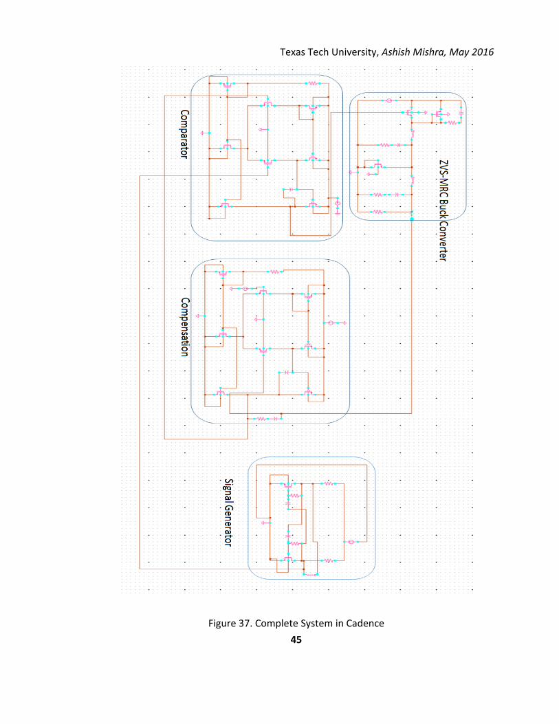
Chapter 6: Complete Circuit of Astable Multivibrator and Resonant Buck Converter
6.1 Results
The figure 37 given below shows the complete circuit for the ZVS-MRC Buck converter
with on chip signal generator. The signal is generated from the astable Multivibrator
shown in figure 38 is given to the comparator for the generation of PWM signal. And this
PWM signal is given to the resonant switch. The frequency of the signal is 1MHz.
Texas Tech University, Ashish Mishra, May 2016
45
Figure 37. Complete System in Cadence

Texas Tech University, Ashish Mishra, May 2016
46
Figure 38. Output of Astable Multivibrator
Some of the components for the converter are very large in values so they cannot be built
on chip. So these components have to be off chip. So, to do so it requires input/output /
input-output ports to do so. Figure 39 shows the ports that are needed to implement it
and the figure 40 gives the proposed chip.

Texas Tech University, Ashish Mishra, May 2016
47
Figure 39. System Schematic after placing Pins

Texas Tech University, Ashish Mishra, May 2016
48
Figure 40. System symbol
Figure 41. Output of the complete system
The curve in the deep blue color colour is the output obtained when the input voltage
was 5V. Yellow curve was obtained then the input voltage was 6V and the pink was
obtained when the input voltage was 8V.

Texas Tech University, Ashish Mishra, May 2016
49
Figure 42. Output from -20°C to 100°C temperature range
The output of the converter if shown in figure 41 after the implementation of the on chip
signal generator. The figure 42 shows the output of the converter at the worst case when
the converter is operated at the lowest duty cycle, here the operating temperature was
done in the range of -20°C to 100°C with a step size of 20°C. The colour graphs obtained
in figure is for the different temperatures i.e., -20°C, 0°C, 20°C, 40°C, 60°C, 80°C and
100°C. From the above two graphs it can be said that the output voltage is constant at
all the different conditions. The layout of the complete chip is shown in figure 43. The
dimension of the chip is 983.4μm X 879.15μm.

Texas Tech University, Ashish Mishra, May 2016
50
Figure 43. System Layout

Texas Tech University, Ashish Mishra, May 2016
51
Table 7. Results
Conventional Buck converter was designed to operate at 1MHz frequency in AMI06
technology to compare the results. As it can be seen from the table 7 that for the resonant
switching converter there is an increase in the stress on the Switch, but at high
frequencies the switching losses are the more dominant than any other types of losses.
So the reduction in the switching losses leads to increase in the efficiency of the converter.

Texas Tech University, Ashish Mishra, May 2016
52
Chapter 7: Future Work: Wireless Power Transfer
7.1 Introduction
There is research going on in the field of wireless power transfer so as to replace the wire,
to power handheld, consumer electronic devices. In the design of wireless power transfer
the concept of coupling of inductor is taken. The power transfer of dc power takes place
from primary to secondary side takes place. The design takes into consideration of 100V
into the primary side and transfers it to the secondary side. The output voltage is passed
through LC filter to remove ripple. Previous literatures focused on the use of power
transfer by AC voltage sources [33-38]. But the portable equipments work mostly on the
DC voltages hence it required an additional rectifier circuit to convert AC voltage into DC
voltage, hence increases the cost of production.
Wireless power transfer is made by combining the Astable Multivibrator, MOSFET and an
inductor. Coupling factor is taken as 0.1 for as distance of 75cm between the coils as
shown in figure 44.
Figure 44. Relation between coupling factor and distance of separation of coils [39]

Texas Tech University, Ashish Mishra, May 2016
53
7.2 Proposed Model
Astable Multivibrator is operated at 8.13 KHz frequency and the output of the Astable
Multivibrator is given to the gate of the MOSFET which works as a switch. Inductor is used
to transfer the power to the secondary side using the principle of mutual coupling of
inductor.
(i)
(ii)
Figure 45. (i) Wireless power transfer circuit (ii) Output voltage of Astable Multivibrator and output voltage on secondary side

Texas Tech University, Ashish Mishra, May 2016
54
Figure 45 shows the schematic of Astable Multivibrator, output of the Multivibrator
given to the gate of the switch and the output voltage of 7V seen across the load
resistance as seen across load resistor

Texas Tech University, Ashish Mishra, May 2016
55
Chapter 8: Conclusion
The DC-DC converter was designed using Zero Voltage Multi Resonant technique. A
conventional and the ZVS-MRC converters were designed and their efficiency were
compared. The switching losses for ZVS scheme was reduced but the voltage stress on
the MOSFET was increased but since the switching was taking place at higher frequencies
hence the voltage stress on the switch has negligible negative effect on the overall
performance of the system. The switching losses are decreased in ZVS scheme so the
efficiency of the system increases as switching losses are dominant at high frequencies.
The Astable Multivibrator was modified from BJTs to MOSFETs as switching device
because the MOSFET can operate at higher frequencies. The Astable Multivibrator was
designed to produce triangular wave ≈1MHz to be fed into the comparator for PWM
generation.
The comparator designed was able to detect the change at its input terminals of 30 𝑉𝜇𝑠⁄
and produce PWM waves accordingly.
The wireless power transfer model proposed is designed to transfer DC voltage of 7V for
a distance of 75cm. The range can be further enhanced by use of repeaters between
transmitting coil and receiving coil.

Texas Tech University, Ashish Mishra, May 2016
56
The future work is to improve this design and achieve efficiency ≈95% and reduce the
voltage stress on the switch. The future work also includes to reduce the size of the
converter further by implementing it on 45nm technology.

Texas Tech University, Ashish Mishra, May 2016
57
References
[1]. Power Electronics and Drives (Version 3-2003) by Dr. Zainal Salam, UTM-JB
[2]. https://en.wikibooks.org/wiki/Power_Electronics
[3]. https://en.wikipedia.org/wiki/DC-to-DC_converter
[4]. https://en.wikipedia.org/wiki/Buck_converter
[5]. Switch Mode Power Supplies by Christophe P. Basso
[6]. http://www.radio-electronics.com/info/power-management/switching-mode-
power-supply/smps-buck-switching-regulator-concept-05.gif
[7]. Power Electronics – Converters, Applications and Design by Ned Mohan, Tore M.
Undeland and Williams P. Robbinson
[8]. http://i.stack.imgur.com/ctDSU.png
[9]. http://www.cadence.com/cadence/Pages/default.aspx
[10] http://www.eit.lth.se/cadsys/chapter1.pdf
[11] http://www.eda.ncsu.edu/wiki/Tutorial:CDK_Layout_Tutorial
[12]. http://www.eda.ncsu.edu/wiki/MOSIS_Layers#Layers_that_correspond_to_op
tional_technology_features:
[13]. https://www.mosis.com/vendors/view/on-semiconductor/c5
[14]. AMI C5N Process Design Rules by Z. Tao and M. Keramat, UNIVERSITY OF
CONNECTICUT
[15]. https://en.wikipedia.org/wiki/Multivibrator#Multivibrator_frequency

Texas Tech University, Ashish Mishra, May 2016
58
[16]. Liu, Kwang-Hwa; Lee, F.C.Y., "Zero-voltage switching technique in DC/DC
converters," Power Electronics, IEEE Transactions on , vol.5, no.3, pp.293,304, Jul
1990
[17]. Ting-Ting Song; Huai Wang; Chung, H.S.-H.; Tapuhi, S.; Ioinovici, A., "A High-
Voltage ZVZCS DC--DC Converter With Low Voltage Stress," Power Electronics,
IEEE Transactions on , vol.23, no.6, pp.2630,2647, Nov. 2008
[18]. Xinke Wu; Xiaogao Xie; Chen Zhao; Zhaoming Qian; Zhao, Rongxiang, "Low
Voltage and Current Stress ZVZCS Full Bridge DC–DC Converter Using Center
Tapped Rectifier Reset," Industrial Electronics, IEEE Transactions on , vol.55, no.3,
pp.1470,1477, March 2008
[19]. Jung-Goo Cho; Ju-Won Baek; Chang-Yong Jeong; Geun-Hie Rim, "Novel zero-
voltage and zero-current-switching full-bridge PWM converter using a simple
auxiliary circuit," Industry Applications, IEEE Transactions on , vol.35, no.1,
pp.15,20, Jan/Feb 1999
[20]. Eung-Ho Kim; Bong-Hwan Kwon, "Zero-Voltage- and Zero-Current-Switching
Full-Bridge Converter With Secondary Resonance," Industrial Electronics, IEEE
Transactions on , vol.57, no.3, pp.1017,1025, March 2010
[21]. Fuxin Liu; Jiajia Yan; Xinbo Ruan, "Zero-Voltage and Zero-Current-Switching
PWM Combined Three-Level DC/DC Converter," Industrial Electronics, IEEE
Transactions on , vol.57, no.5, pp.1644,1654, May 2010

Texas Tech University, Ashish Mishra, May 2016
59
[22]. Woo-Jin Lee; Chong-Eun Kim; Sang-Kyoo Han; Gun-Woo Moon, "A New High
Efficiency Phase Shifted Full Bridge Converter for Sustaining Power Module of
Plasma Display Panel," Power Electronics Specialists Conference, 2005. PESC '05.
IEEE 36th , vol., no., pp.2630,2634, 16-16 June 2005
[23]. Kyung-Hwa Park; Kang-Hyun Yi, "A Wide Load Range ZVS Dual Half-Bridge
Converters for Large-Sized PDP Sustaining Power Modules," Display Technology,
Journal of , vol.11, no.1, pp.86,96, Jan. 2015
[24]. Rashid, Muhammad H... Power Electronics Handbook Devices, Circuits and
Applications = Edited by Muhammad H. Rashid, Amsterdam: Elsevier, 2011. Print.
[25]. Hui, S. Y.(Ron), and Henry S.h. Chung. "Resonant and Soft-switching Converters."
Power Electronics Handbook (2007): 405-49. Web.
[26]. Tabisz, W.A.; Lee, F.C., "Zero-voltage-switching multi-resonant technique-a
novel approach to improve performance of high frequency quasi-resonant
converters," Power Electronics Specialists Conference, 1988. PESC '88 Record.,
19th Annual IEEE , vol., no., pp.9,17 vol.1, 11-14 April 1988
[27]. Patni, Purvi. Integrated Power Supply. Thesis. Texas Tech University, 2012. N.p.:
n.p., n.d. Web. 9 June 2015. <http://repositories.tdl.org/ttu-
ir/handle/2346/47507>.
[28]. https://en.wikipedia.org/wiki/Operational_amplifier
[29]. "Design of Analog CMOS Integrated Circuits 1st Edition." Design of Analog CMOS
Integrated Circuits: Behzad Razavi: 9780072380323: Amazon.com: Books. N.p.,

Texas Tech University, Ashish Mishra, May 2016
60
n.d. Web. 15 Feb. 2016. <http://www.amazon.com/Design-Analog-CMOS-
Integrated-Circuits/dp/0072380322>.
[30]. http://www.learnabout-electronics.org/Amplifiers/amplifiers64.php
[31]. http://www.edaboard.com/thread330450.html
[32]. http://www.spiceopus.si/imgopt/opt006-01.gif
[33]. Hoang, N.K.; Sang-Gug Lee, "A method of regulating wireless power transfer
based on the analysis of power communication," in Emerging Technologies:
Wireless Power (WoW), 2015 IEEE PELS Workshop on , vol., no., pp.1-3, 5-6 June
2015
[34]. Awai, I.; Ishizaki, T., "Superiority of BPF theory for design of coupled resonator
WPT systems," in Microwave Conference Proceedings (APMC), 2011 Asia-Pacific ,
vol., no., pp.1889-1892, 5-8 Dec. 2011
[35]. Bodrov, Alexey, and Seung-Ki Sul. "Analysis of Wireless Power Transfer by
Coupled Mode Theory (CMT) and Practical Considerations to Increase Power
Transfer Efficiency." Wireless Power Transfer - Principles and Engineering
Explorations (2012): n. pag. Web.
[36]. Matias, R.; Cunha, B.; Martins, R., "Modeling inductive coupling for Wireless
Power Transfer to integrated circuits," in Wireless Power Transfer (WPT), 2013
IEEE , vol., no., pp.198-201, 15-16 May 2013
[37]. Kato, Masaki, Takehiro Imura, and Yoichi Hori. "Study on Maximize Efficiency
by Secondary Side Control Using DC-DC Converter in Wireless Power Transfer via

Texas Tech University, Ashish Mishra, May 2016
61
Magnetic Resonant Coupling." 2013 World Electric Vehicle Symposium and
Exhibition (EVS27) (2013): n. pag. Web.
[38]. Tsunekawa, K., "A feasibility study of wireless power transmission system by
using two independent coupled electric fields," in Microwave Workshop Series
on Innovative Wireless Power Transmission: Technologies, Systems, and
Applications (IMWS), 2011 IEEE MTT-S International , vol., no., pp.141-144, 12-13
May 2011
[39]. Kurs, A., A. Karalis, R. Moffatt, J. D. Joannopoulos, P. Fisher, and M. Soljacic.
"Wireless Power Transfer via Strongly Coupled Magnetic Resonances." Science
317.5834 (2007): 83-86. Web.